EP2498130A2 - Curable composition for solid-state imaging device, and photosensitive layer, permanent pattern, wafer-level lens, solid-state imaging device and pattern forming method each using the composition - Google Patents
Curable composition for solid-state imaging device, and photosensitive layer, permanent pattern, wafer-level lens, solid-state imaging device and pattern forming method each using the composition Download PDFInfo
- Publication number
- EP2498130A2 EP2498130A2 EP12158562A EP12158562A EP2498130A2 EP 2498130 A2 EP2498130 A2 EP 2498130A2 EP 12158562 A EP12158562 A EP 12158562A EP 12158562 A EP12158562 A EP 12158562A EP 2498130 A2 EP2498130 A2 EP 2498130A2
- Authority
- EP
- European Patent Office
- Prior art keywords
- group
- compound
- solid
- imaging device
- state imaging
- Prior art date
- Legal status (The legal status is an assumption and is not a legal conclusion. Google has not performed a legal analysis and makes no representation as to the accuracy of the status listed.)
- Withdrawn
Links
- 239000000203 mixture Substances 0.000 title claims abstract description 165
- 238000003384 imaging method Methods 0.000 title claims abstract description 156
- 238000000034 method Methods 0.000 title claims description 74
- 150000001875 compounds Chemical class 0.000 claims abstract description 225
- 229920005989 resin Polymers 0.000 claims abstract description 111
- 239000011347 resin Substances 0.000 claims abstract description 111
- 239000011230 binding agent Substances 0.000 claims abstract description 80
- 239000002253 acid Substances 0.000 claims abstract description 78
- 239000000463 material Substances 0.000 claims abstract description 39
- 238000004132 cross linking Methods 0.000 claims abstract description 34
- 238000006243 chemical reaction Methods 0.000 claims abstract description 19
- 230000005855 radiation Effects 0.000 claims abstract description 18
- 230000009471 action Effects 0.000 claims abstract description 11
- -1 salt compound Chemical class 0.000 claims description 169
- 239000000758 substrate Substances 0.000 claims description 127
- 229910000679 solder Inorganic materials 0.000 claims description 74
- 238000011161 development Methods 0.000 claims description 47
- 239000003513 alkali Substances 0.000 claims description 35
- ISWSIDIOOBJBQZ-UHFFFAOYSA-N phenol group Chemical group C1(=CC=CC=C1)O ISWSIDIOOBJBQZ-UHFFFAOYSA-N 0.000 claims description 33
- 150000003658 tungsten compounds Chemical class 0.000 claims description 18
- 125000004849 alkoxymethyl group Chemical group 0.000 claims description 17
- 229920002647 polyamide Polymers 0.000 claims description 17
- 125000004029 hydroxymethyl group Chemical group [H]OC([H])([H])* 0.000 claims description 15
- 229920001721 polyimide Polymers 0.000 claims description 10
- 125000000466 oxiranyl group Chemical group 0.000 claims description 8
- 239000004642 Polyimide Substances 0.000 claims description 6
- 229920002803 thermoplastic polyurethane Polymers 0.000 claims description 3
- 239000010408 film Substances 0.000 description 112
- 239000010410 layer Substances 0.000 description 99
- 229920000642 polymer Polymers 0.000 description 64
- 239000004593 Epoxy Substances 0.000 description 63
- 125000001424 substituent group Chemical group 0.000 description 61
- 125000000217 alkyl group Chemical group 0.000 description 57
- 229910052799 carbon Inorganic materials 0.000 description 52
- OKTJSMMVPCPJKN-UHFFFAOYSA-N Carbon Chemical compound [C] OKTJSMMVPCPJKN-UHFFFAOYSA-N 0.000 description 50
- 239000000243 solution Substances 0.000 description 47
- 230000018109 developmental process Effects 0.000 description 46
- 229910052751 metal Inorganic materials 0.000 description 46
- 239000002184 metal Substances 0.000 description 45
- NIXOWILDQLNWCW-UHFFFAOYSA-M Acrylate Chemical compound [O-]C(=O)C=C NIXOWILDQLNWCW-UHFFFAOYSA-M 0.000 description 40
- 125000003118 aryl group Chemical group 0.000 description 39
- 230000000694 effects Effects 0.000 description 38
- 238000000576 coating method Methods 0.000 description 36
- 229920001971 elastomer Polymers 0.000 description 36
- VYPSYNLAJGMNEJ-UHFFFAOYSA-N Silicium dioxide Chemical compound O=[Si]=O VYPSYNLAJGMNEJ-UHFFFAOYSA-N 0.000 description 35
- 229920001577 copolymer Polymers 0.000 description 34
- 239000011248 coating agent Substances 0.000 description 33
- 125000004435 hydrogen atom Chemical group [H]* 0.000 description 32
- 239000011247 coating layer Substances 0.000 description 31
- 238000001723 curing Methods 0.000 description 31
- 239000000806 elastomer Substances 0.000 description 31
- 125000003700 epoxy group Chemical group 0.000 description 27
- 125000003178 carboxy group Chemical group [H]OC(*)=O 0.000 description 26
- 239000000178 monomer Substances 0.000 description 26
- 238000010438 heat treatment Methods 0.000 description 25
- 125000002887 hydroxy group Chemical group [H]O* 0.000 description 25
- 239000012778 molding material Substances 0.000 description 24
- XUIMIQQOPSSXEZ-UHFFFAOYSA-N Silicon Chemical compound [Si] XUIMIQQOPSSXEZ-UHFFFAOYSA-N 0.000 description 23
- 229910052710 silicon Inorganic materials 0.000 description 23
- 239000010703 silicon Substances 0.000 description 23
- 239000004094 surface-active agent Substances 0.000 description 23
- 230000015572 biosynthetic process Effects 0.000 description 22
- IISBACLAFKSPIT-UHFFFAOYSA-N bisphenol A Chemical compound C=1C=C(O)C=CC=1C(C)(C)C1=CC=C(O)C=C1 IISBACLAFKSPIT-UHFFFAOYSA-N 0.000 description 22
- CERQOIWHTDAKMF-UHFFFAOYSA-N Methacrylic acid Chemical compound CC(=C)C(O)=O CERQOIWHTDAKMF-UHFFFAOYSA-N 0.000 description 20
- 239000002270 dispersing agent Substances 0.000 description 20
- 239000000945 filler Substances 0.000 description 20
- 229920000728 polyester Polymers 0.000 description 20
- 229920001296 polysiloxane Polymers 0.000 description 20
- 239000000975 dye Substances 0.000 description 18
- 239000002904 solvent Substances 0.000 description 18
- ARXJGSRGQADJSQ-UHFFFAOYSA-N 1-methoxypropan-2-ol Chemical compound COCC(C)O ARXJGSRGQADJSQ-UHFFFAOYSA-N 0.000 description 17
- 239000000377 silicon dioxide Substances 0.000 description 17
- 229930185605 Bisphenol Natural products 0.000 description 16
- PPBRXRYQALVLMV-UHFFFAOYSA-N Styrene Chemical compound C=CC1=CC=CC=C1 PPBRXRYQALVLMV-UHFFFAOYSA-N 0.000 description 16
- 239000006185 dispersion Substances 0.000 description 16
- 239000011521 glass Substances 0.000 description 16
- 239000007787 solid Substances 0.000 description 16
- 239000000126 substance Substances 0.000 description 16
- 239000006087 Silane Coupling Agent Substances 0.000 description 15
- 125000000524 functional group Chemical group 0.000 description 15
- 238000004519 manufacturing process Methods 0.000 description 15
- 239000002585 base Substances 0.000 description 14
- 239000002245 particle Substances 0.000 description 14
- 230000035939 shock Effects 0.000 description 14
- 125000002496 methyl group Chemical group [H]C([H])([H])* 0.000 description 13
- 230000035945 sensitivity Effects 0.000 description 12
- 125000003342 alkenyl group Chemical group 0.000 description 11
- 239000003795 chemical substances by application Substances 0.000 description 11
- 125000001997 phenyl group Chemical group [H]C1=C([H])C([H])=C(*)C([H])=C1[H] 0.000 description 11
- LYCAIKOWRPUZTN-UHFFFAOYSA-N Ethylene glycol Chemical compound OCCO LYCAIKOWRPUZTN-UHFFFAOYSA-N 0.000 description 10
- OFOBLEOULBTSOW-UHFFFAOYSA-N Propanedioic acid Natural products OC(=O)CC(O)=O OFOBLEOULBTSOW-UHFFFAOYSA-N 0.000 description 10
- 125000003647 acryloyl group Chemical group O=C([*])C([H])=C([H])[H] 0.000 description 10
- 125000003277 amino group Chemical group 0.000 description 10
- 238000004140 cleaning Methods 0.000 description 10
- 239000010419 fine particle Substances 0.000 description 10
- 238000000206 photolithography Methods 0.000 description 10
- 230000009257 reactivity Effects 0.000 description 10
- XLYOFNOQVPJJNP-UHFFFAOYSA-N water Substances O XLYOFNOQVPJJNP-UHFFFAOYSA-N 0.000 description 10
- 239000004925 Acrylic resin Substances 0.000 description 9
- 229920000178 Acrylic resin Polymers 0.000 description 9
- 229920000459 Nitrile rubber Polymers 0.000 description 9
- 239000004952 Polyamide Substances 0.000 description 9
- 238000001035 drying Methods 0.000 description 9
- 239000011229 interlayer Substances 0.000 description 9
- 239000007788 liquid Substances 0.000 description 9
- QSHDDOUJBYECFT-UHFFFAOYSA-N mercury Chemical compound [Hg] QSHDDOUJBYECFT-UHFFFAOYSA-N 0.000 description 9
- 229910052753 mercury Inorganic materials 0.000 description 9
- 125000000962 organic group Chemical group 0.000 description 9
- 230000008569 process Effects 0.000 description 9
- 150000003254 radicals Chemical class 0.000 description 9
- YCKRFDGAMUMZLT-UHFFFAOYSA-N Fluorine atom Chemical compound [F] YCKRFDGAMUMZLT-UHFFFAOYSA-N 0.000 description 8
- 238000010521 absorption reaction Methods 0.000 description 8
- 125000004453 alkoxycarbonyl group Chemical group 0.000 description 8
- 239000010949 copper Substances 0.000 description 8
- 229910052731 fluorine Inorganic materials 0.000 description 8
- 239000011737 fluorine Substances 0.000 description 8
- 125000000623 heterocyclic group Chemical group 0.000 description 8
- CBOIHMRHGLHBPB-UHFFFAOYSA-N hydroxymethyl Chemical group O[CH2] CBOIHMRHGLHBPB-UHFFFAOYSA-N 0.000 description 8
- 229920000647 polyepoxide Polymers 0.000 description 8
- 150000003839 salts Chemical class 0.000 description 8
- WGTYBPLFGIVFAS-UHFFFAOYSA-M tetramethylammonium hydroxide Chemical compound [OH-].C[N+](C)(C)C WGTYBPLFGIVFAS-UHFFFAOYSA-M 0.000 description 8
- LFQSCWFLJHTTHZ-UHFFFAOYSA-N Ethanol Chemical compound CCO LFQSCWFLJHTTHZ-UHFFFAOYSA-N 0.000 description 7
- 229920003171 Poly (ethylene oxide) Polymers 0.000 description 7
- 239000004721 Polyphenylene oxide Substances 0.000 description 7
- 239000000853 adhesive Substances 0.000 description 7
- 230000001070 adhesive effect Effects 0.000 description 7
- 125000003545 alkoxy group Chemical group 0.000 description 7
- 239000003086 colorant Substances 0.000 description 7
- 229910052802 copper Inorganic materials 0.000 description 7
- 239000003431 cross linking reagent Substances 0.000 description 7
- 230000002708 enhancing effect Effects 0.000 description 7
- 239000003822 epoxy resin Substances 0.000 description 7
- VOZRXNHHFUQHIL-UHFFFAOYSA-N glycidyl methacrylate Chemical compound CC(=C)C(=O)OCC1CO1 VOZRXNHHFUQHIL-UHFFFAOYSA-N 0.000 description 7
- 229920000578 graft copolymer Polymers 0.000 description 7
- IQPQWNKOIGAROB-UHFFFAOYSA-N isocyanate group Chemical group [N-]=C=O IQPQWNKOIGAROB-UHFFFAOYSA-N 0.000 description 7
- 238000000465 moulding Methods 0.000 description 7
- 125000003566 oxetanyl group Chemical group 0.000 description 7
- 229920001568 phenolic resin Polymers 0.000 description 7
- 229920000570 polyether Polymers 0.000 description 7
- 235000013824 polyphenols Nutrition 0.000 description 7
- 229920005749 polyurethane resin Polymers 0.000 description 7
- LLHKCFNBLRBOGN-UHFFFAOYSA-N propylene glycol methyl ether acetate Chemical compound COCC(C)OC(C)=O LLHKCFNBLRBOGN-UHFFFAOYSA-N 0.000 description 7
- 230000007261 regionalization Effects 0.000 description 7
- 238000003860 storage Methods 0.000 description 7
- MYRTYDVEIRVNKP-UHFFFAOYSA-N 1,2-Divinylbenzene Chemical compound C=CC1=CC=CC=C1C=C MYRTYDVEIRVNKP-UHFFFAOYSA-N 0.000 description 6
- JOYRKODLDBILNP-UHFFFAOYSA-N Ethyl urethane Chemical compound CCOC(N)=O JOYRKODLDBILNP-UHFFFAOYSA-N 0.000 description 6
- XEEYBQQBJWHFJM-UHFFFAOYSA-N Iron Chemical compound [Fe] XEEYBQQBJWHFJM-UHFFFAOYSA-N 0.000 description 6
- OKKJLVBELUTLKV-UHFFFAOYSA-N Methanol Chemical compound OC OKKJLVBELUTLKV-UHFFFAOYSA-N 0.000 description 6
- ZMXDDKWLCZADIW-UHFFFAOYSA-N N,N-Dimethylformamide Chemical compound CN(C)C=O ZMXDDKWLCZADIW-UHFFFAOYSA-N 0.000 description 6
- SECXISVLQFMRJM-UHFFFAOYSA-N N-Methylpyrrolidone Chemical compound CN1CCCC1=O SECXISVLQFMRJM-UHFFFAOYSA-N 0.000 description 6
- NBIIXXVUZAFLBC-UHFFFAOYSA-N Phosphoric acid Chemical compound OP(O)(O)=O NBIIXXVUZAFLBC-UHFFFAOYSA-N 0.000 description 6
- 125000002252 acyl group Chemical group 0.000 description 6
- 125000004104 aryloxy group Chemical group 0.000 description 6
- PXKLMJQFEQBVLD-UHFFFAOYSA-N bisphenol F Chemical compound C1=CC(O)=CC=C1CC1=CC=C(O)C=C1 PXKLMJQFEQBVLD-UHFFFAOYSA-N 0.000 description 6
- 150000001732 carboxylic acid derivatives Chemical class 0.000 description 6
- 125000004093 cyano group Chemical group *C#N 0.000 description 6
- 150000002009 diols Chemical class 0.000 description 6
- 238000010894 electron beam technology Methods 0.000 description 6
- 125000001495 ethyl group Chemical group [H]C([H])([H])C([H])([H])* 0.000 description 6
- 238000011156 evaluation Methods 0.000 description 6
- SLGWESQGEUXWJQ-UHFFFAOYSA-N formaldehyde;phenol Chemical compound O=C.OC1=CC=CC=C1 SLGWESQGEUXWJQ-UHFFFAOYSA-N 0.000 description 6
- 125000003055 glycidyl group Chemical group C(C1CO1)* 0.000 description 6
- 125000005843 halogen group Chemical group 0.000 description 6
- RAXXELZNTBOGNW-UHFFFAOYSA-N imidazole Natural products C1=CNC=N1 RAXXELZNTBOGNW-UHFFFAOYSA-N 0.000 description 6
- 125000001624 naphthyl group Chemical group 0.000 description 6
- QGLKJKCYBOYXKC-UHFFFAOYSA-N nonaoxidotritungsten Chemical compound O=[W]1(=O)O[W](=O)(=O)O[W](=O)(=O)O1 QGLKJKCYBOYXKC-UHFFFAOYSA-N 0.000 description 6
- 229920000058 polyacrylate Polymers 0.000 description 6
- 238000002360 preparation method Methods 0.000 description 6
- 238000003786 synthesis reaction Methods 0.000 description 6
- 238000012360 testing method Methods 0.000 description 6
- 238000002834 transmittance Methods 0.000 description 6
- 229910052721 tungsten Inorganic materials 0.000 description 6
- 229910001930 tungsten oxide Inorganic materials 0.000 description 6
- 229920002554 vinyl polymer Polymers 0.000 description 6
- 229920002126 Acrylic acid copolymer Polymers 0.000 description 5
- PEDCQBHIVMGVHV-UHFFFAOYSA-N Glycerine Chemical compound OCC(O)CO PEDCQBHIVMGVHV-UHFFFAOYSA-N 0.000 description 5
- 150000008065 acid anhydrides Chemical class 0.000 description 5
- 239000012670 alkaline solution Substances 0.000 description 5
- 125000003282 alkyl amino group Chemical group 0.000 description 5
- 125000000304 alkynyl group Chemical group 0.000 description 5
- 150000001450 anions Chemical class 0.000 description 5
- 125000001797 benzyl group Chemical group [H]C1=C([H])C([H])=C(C([H])=C1[H])C([H])([H])* 0.000 description 5
- 239000003054 catalyst Substances 0.000 description 5
- 239000007795 chemical reaction product Substances 0.000 description 5
- 150000004292 cyclic ethers Chemical group 0.000 description 5
- WSFSSNUMVMOOMR-UHFFFAOYSA-N formaldehyde Substances O=C WSFSSNUMVMOOMR-UHFFFAOYSA-N 0.000 description 5
- 239000004973 liquid crystal related substance Substances 0.000 description 5
- 239000011976 maleic acid Substances 0.000 description 5
- 125000000449 nitro group Chemical group [O-][N+](*)=O 0.000 description 5
- 125000004430 oxygen atom Chemical group O* 0.000 description 5
- 229920006124 polyolefin elastomer Polymers 0.000 description 5
- 239000005060 rubber Substances 0.000 description 5
- 238000003756 stirring Methods 0.000 description 5
- 238000004381 surface treatment Methods 0.000 description 5
- 229910052719 titanium Inorganic materials 0.000 description 5
- 239000010936 titanium Substances 0.000 description 5
- VZCYOOQTPOCHFL-UHFFFAOYSA-N trans-butenedioic acid Natural products OC(=O)C=CC(O)=O VZCYOOQTPOCHFL-UHFFFAOYSA-N 0.000 description 5
- WFKWXMTUELFFGS-UHFFFAOYSA-N tungsten Chemical compound [W] WFKWXMTUELFFGS-UHFFFAOYSA-N 0.000 description 5
- 239000010937 tungsten Substances 0.000 description 5
- 239000004711 α-olefin Substances 0.000 description 5
- VVBLNCFGVYUYGU-UHFFFAOYSA-N 4,4'-Bis(dimethylamino)benzophenone Chemical compound C1=CC(N(C)C)=CC=C1C(=O)C1=CC=C(N(C)C)C=C1 VVBLNCFGVYUYGU-UHFFFAOYSA-N 0.000 description 4
- QUSNBJAOOMFDIB-UHFFFAOYSA-N Ethylamine Chemical compound CCN QUSNBJAOOMFDIB-UHFFFAOYSA-N 0.000 description 4
- UQSXHKLRYXJYBZ-UHFFFAOYSA-N Iron oxide Chemical compound [Fe]=O UQSXHKLRYXJYBZ-UHFFFAOYSA-N 0.000 description 4
- KFZMGEQAYNKOFK-UHFFFAOYSA-N Isopropanol Chemical compound CC(C)O KFZMGEQAYNKOFK-UHFFFAOYSA-N 0.000 description 4
- NQRYJNQNLNOLGT-UHFFFAOYSA-N Piperidine Chemical compound C1CCNCC1 NQRYJNQNLNOLGT-UHFFFAOYSA-N 0.000 description 4
- 239000005062 Polybutadiene Substances 0.000 description 4
- 239000002202 Polyethylene glycol Substances 0.000 description 4
- 239000004793 Polystyrene Substances 0.000 description 4
- KAESVJOAVNADME-UHFFFAOYSA-N Pyrrole Chemical compound C=1C=CNC=1 KAESVJOAVNADME-UHFFFAOYSA-N 0.000 description 4
- WYURNTSHIVDZCO-UHFFFAOYSA-N Tetrahydrofuran Chemical compound C1CCOC1 WYURNTSHIVDZCO-UHFFFAOYSA-N 0.000 description 4
- 125000002777 acetyl group Chemical group [H]C([H])([H])C(*)=O 0.000 description 4
- 230000002378 acidificating effect Effects 0.000 description 4
- 238000007259 addition reaction Methods 0.000 description 4
- 125000002723 alicyclic group Chemical group 0.000 description 4
- 125000004390 alkyl sulfonyl group Chemical group 0.000 description 4
- 238000000149 argon plasma sintering Methods 0.000 description 4
- 125000003710 aryl alkyl group Chemical group 0.000 description 4
- 125000001769 aryl amino group Chemical group 0.000 description 4
- 125000004391 aryl sulfonyl group Chemical group 0.000 description 4
- NTXGQCSETZTARF-UHFFFAOYSA-N buta-1,3-diene;prop-2-enenitrile Chemical compound C=CC=C.C=CC#N NTXGQCSETZTARF-UHFFFAOYSA-N 0.000 description 4
- WERYXYBDKMZEQL-UHFFFAOYSA-N butane-1,4-diol Chemical compound OCCCCO WERYXYBDKMZEQL-UHFFFAOYSA-N 0.000 description 4
- 239000013065 commercial product Substances 0.000 description 4
- JHIVVAPYMSGYDF-UHFFFAOYSA-N cyclohexanone Chemical compound O=C1CCCCC1 JHIVVAPYMSGYDF-UHFFFAOYSA-N 0.000 description 4
- 238000009792 diffusion process Methods 0.000 description 4
- 150000002148 esters Chemical class 0.000 description 4
- RTZKZFJDLAIYFH-UHFFFAOYSA-N ether Substances CCOCC RTZKZFJDLAIYFH-UHFFFAOYSA-N 0.000 description 4
- 229910052739 hydrogen Chemical group 0.000 description 4
- 230000001965 increasing effect Effects 0.000 description 4
- 229910052742 iron Inorganic materials 0.000 description 4
- 239000012948 isocyanate Substances 0.000 description 4
- 125000005647 linker group Chemical group 0.000 description 4
- JDSHMPZPIAZGSV-UHFFFAOYSA-N melamine Chemical group NC1=NC(N)=NC(N)=N1 JDSHMPZPIAZGSV-UHFFFAOYSA-N 0.000 description 4
- 125000000325 methylidene group Chemical group [H]C([H])=* 0.000 description 4
- 238000002156 mixing Methods 0.000 description 4
- PXHVJJICTQNCMI-UHFFFAOYSA-N nickel Substances [Ni] PXHVJJICTQNCMI-UHFFFAOYSA-N 0.000 description 4
- 229920003986 novolac Polymers 0.000 description 4
- 239000005011 phenolic resin Substances 0.000 description 4
- 239000000049 pigment Substances 0.000 description 4
- 229920006122 polyamide resin Polymers 0.000 description 4
- 229920002857 polybutadiene Polymers 0.000 description 4
- 229920001223 polyethylene glycol Polymers 0.000 description 4
- 239000009719 polyimide resin Substances 0.000 description 4
- 229920001228 polyisocyanate Polymers 0.000 description 4
- 239000005056 polyisocyanate Substances 0.000 description 4
- 229920002223 polystyrene Polymers 0.000 description 4
- 230000009467 reduction Effects 0.000 description 4
- 239000004065 semiconductor Substances 0.000 description 4
- 238000004528 spin coating Methods 0.000 description 4
- 125000000020 sulfo group Chemical group O=S(=O)([*])O[H] 0.000 description 4
- LDHQCZJRKDOVOX-UHFFFAOYSA-N trans-crotonic acid Natural products CC=CC(O)=O LDHQCZJRKDOVOX-UHFFFAOYSA-N 0.000 description 4
- RIOQSEWOXXDEQQ-UHFFFAOYSA-N triphenylphosphine Chemical compound C1=CC=CC=C1P(C=1C=CC=CC=1)C1=CC=CC=C1 RIOQSEWOXXDEQQ-UHFFFAOYSA-N 0.000 description 4
- 125000000391 vinyl group Chemical group [H]C([*])=C([H])[H] 0.000 description 4
- JIHQDMXYYFUGFV-UHFFFAOYSA-N 1,3,5-triazine Chemical class C1=NC=NC=N1 JIHQDMXYYFUGFV-UHFFFAOYSA-N 0.000 description 3
- SMZOUWXMTYCWNB-UHFFFAOYSA-N 2-(2-methoxy-5-methylphenyl)ethanamine Chemical compound COC1=CC=C(C)C=C1CCN SMZOUWXMTYCWNB-UHFFFAOYSA-N 0.000 description 3
- ZWEHNKRNPOVVGH-UHFFFAOYSA-N 2-Butanone Chemical compound CCC(C)=O ZWEHNKRNPOVVGH-UHFFFAOYSA-N 0.000 description 3
- NIXOWILDQLNWCW-UHFFFAOYSA-N 2-Propenoic acid Natural products OC(=O)C=C NIXOWILDQLNWCW-UHFFFAOYSA-N 0.000 description 3
- QTWJRLJHJPIABL-UHFFFAOYSA-N 2-methylphenol;3-methylphenol;4-methylphenol Chemical compound CC1=CC=C(O)C=C1.CC1=CC=CC(O)=C1.CC1=CC=CC=C1O QTWJRLJHJPIABL-UHFFFAOYSA-N 0.000 description 3
- MILSYCKGLDDVLM-UHFFFAOYSA-N 2-phenylpropan-2-ylbenzene Chemical group C=1C=CC=CC=1C(C)(C)C1=CC=CC=C1 MILSYCKGLDDVLM-UHFFFAOYSA-N 0.000 description 3
- 125000003903 2-propenyl group Chemical group [H]C([*])([H])C([H])=C([H])[H] 0.000 description 3
- VPWNQTHUCYMVMZ-UHFFFAOYSA-N 4,4'-sulfonyldiphenol Chemical compound C1=CC(O)=CC=C1S(=O)(=O)C1=CC=C(O)C=C1 VPWNQTHUCYMVMZ-UHFFFAOYSA-N 0.000 description 3
- CSCPPACGZOOCGX-UHFFFAOYSA-N Acetone Chemical compound CC(C)=O CSCPPACGZOOCGX-UHFFFAOYSA-N 0.000 description 3
- NLHHRLWOUZZQLW-UHFFFAOYSA-N Acrylonitrile Chemical compound C=CC#N NLHHRLWOUZZQLW-UHFFFAOYSA-N 0.000 description 3
- UHOVQNZJYSORNB-UHFFFAOYSA-N Benzene Chemical compound C1=CC=CC=C1 UHOVQNZJYSORNB-UHFFFAOYSA-N 0.000 description 3
- RYGMFSIKBFXOCR-UHFFFAOYSA-N Copper Chemical compound [Cu] RYGMFSIKBFXOCR-UHFFFAOYSA-N 0.000 description 3
- 229920000089 Cyclic olefin copolymer Polymers 0.000 description 3
- YMWUJEATGCHHMB-UHFFFAOYSA-N Dichloromethane Chemical compound ClCCl YMWUJEATGCHHMB-UHFFFAOYSA-N 0.000 description 3
- BRLQWZUYTZBJKN-UHFFFAOYSA-N Epichlorohydrin Chemical compound ClCC1CO1 BRLQWZUYTZBJKN-UHFFFAOYSA-N 0.000 description 3
- XEKOWRVHYACXOJ-UHFFFAOYSA-N Ethyl acetate Chemical compound CCOC(C)=O XEKOWRVHYACXOJ-UHFFFAOYSA-N 0.000 description 3
- KWYUFKZDYYNOTN-UHFFFAOYSA-M Potassium hydroxide Chemical compound [OH-].[K+] KWYUFKZDYYNOTN-UHFFFAOYSA-M 0.000 description 3
- DNIAPMSPPWPWGF-UHFFFAOYSA-N Propylene glycol Chemical compound CC(O)CO DNIAPMSPPWPWGF-UHFFFAOYSA-N 0.000 description 3
- HEMHJVSKTPXQMS-UHFFFAOYSA-M Sodium hydroxide Chemical compound [OH-].[Na+] HEMHJVSKTPXQMS-UHFFFAOYSA-M 0.000 description 3
- YXFVVABEGXRONW-UHFFFAOYSA-N Toluene Chemical compound CC1=CC=CC=C1 YXFVVABEGXRONW-UHFFFAOYSA-N 0.000 description 3
- 229920000800 acrylic rubber Polymers 0.000 description 3
- 125000001931 aliphatic group Chemical group 0.000 description 3
- 229910052783 alkali metal Inorganic materials 0.000 description 3
- 150000001340 alkali metals Chemical class 0.000 description 3
- 125000002947 alkylene group Chemical group 0.000 description 3
- 150000001412 amines Chemical class 0.000 description 3
- 239000003945 anionic surfactant Substances 0.000 description 3
- 239000012298 atmosphere Substances 0.000 description 3
- TZCXTZWJZNENPQ-UHFFFAOYSA-L barium sulfate Chemical compound [Ba+2].[O-]S([O-])(=O)=O TZCXTZWJZNENPQ-UHFFFAOYSA-L 0.000 description 3
- RWCCWEUUXYIKHB-UHFFFAOYSA-N benzophenone Chemical group C=1C=CC=CC=1C(=O)C1=CC=CC=C1 RWCCWEUUXYIKHB-UHFFFAOYSA-N 0.000 description 3
- 239000006229 carbon black Substances 0.000 description 3
- 239000003093 cationic surfactant Substances 0.000 description 3
- 230000001413 cellular effect Effects 0.000 description 3
- 229910052804 chromium Inorganic materials 0.000 description 3
- 239000011651 chromium Substances 0.000 description 3
- 229930003836 cresol Natural products 0.000 description 3
- 125000004122 cyclic group Chemical group 0.000 description 3
- 125000004663 dialkyl amino group Chemical group 0.000 description 3
- 235000014113 dietary fatty acids Nutrition 0.000 description 3
- USIUVYZYUHIAEV-UHFFFAOYSA-N diphenyl ether Chemical group C=1C=CC=CC=1OC1=CC=CC=C1 USIUVYZYUHIAEV-UHFFFAOYSA-N 0.000 description 3
- KZTYYGOKRVBIMI-UHFFFAOYSA-N diphenyl sulfone Chemical group C=1C=CC=CC=1S(=O)(=O)C1=CC=CC=C1 KZTYYGOKRVBIMI-UHFFFAOYSA-N 0.000 description 3
- JBKVHLHDHHXQEQ-UHFFFAOYSA-N epsilon-caprolactam Chemical compound O=C1CCCCCN1 JBKVHLHDHHXQEQ-UHFFFAOYSA-N 0.000 description 3
- 239000000194 fatty acid Substances 0.000 description 3
- 229930195729 fatty acid Natural products 0.000 description 3
- 229910052737 gold Inorganic materials 0.000 description 3
- 239000010931 gold Substances 0.000 description 3
- RRAMGCGOFNQTLD-UHFFFAOYSA-N hexamethylene diisocyanate Chemical compound O=C=NCCCCCCN=C=O RRAMGCGOFNQTLD-UHFFFAOYSA-N 0.000 description 3
- WGCNASOHLSPBMP-UHFFFAOYSA-N hydroxyacetaldehyde Natural products OCC=O WGCNASOHLSPBMP-UHFFFAOYSA-N 0.000 description 3
- 239000003999 initiator Substances 0.000 description 3
- 150000002513 isocyanates Chemical class 0.000 description 3
- 125000001449 isopropyl group Chemical group [H]C([H])([H])C([H])(*)C([H])([H])[H] 0.000 description 3
- 229910052748 manganese Inorganic materials 0.000 description 3
- 239000011572 manganese Substances 0.000 description 3
- LVHBHZANLOWSRM-UHFFFAOYSA-N methylenebutanedioic acid Natural products OC(=O)CC(=C)C(O)=O LVHBHZANLOWSRM-UHFFFAOYSA-N 0.000 description 3
- SNVLJLYUUXKWOJ-UHFFFAOYSA-N methylidenecarbene Chemical compound C=[C] SNVLJLYUUXKWOJ-UHFFFAOYSA-N 0.000 description 3
- 239000012046 mixed solvent Substances 0.000 description 3
- 229910052759 nickel Inorganic materials 0.000 description 3
- 229910052757 nitrogen Inorganic materials 0.000 description 3
- 239000002736 nonionic surfactant Substances 0.000 description 3
- 229920000620 organic polymer Polymers 0.000 description 3
- 238000000059 patterning Methods 0.000 description 3
- 125000002080 perylenyl group Chemical group C1(=CC=C2C=CC=C3C4=CC=CC5=CC=CC(C1=C23)=C45)* 0.000 description 3
- 150000002989 phenols Chemical class 0.000 description 3
- 229910052698 phosphorus Inorganic materials 0.000 description 3
- 239000011574 phosphorus Substances 0.000 description 3
- IEQIEDJGQAUEQZ-UHFFFAOYSA-N phthalocyanine Chemical class N1C(N=C2C3=CC=CC=C3C(N=C3C4=CC=CC=C4C(=N4)N3)=N2)=C(C=CC=C2)C2=C1N=C1C2=CC=CC=C2C4=N1 IEQIEDJGQAUEQZ-UHFFFAOYSA-N 0.000 description 3
- 229920005575 poly(amic acid) Polymers 0.000 description 3
- 239000011164 primary particle Substances 0.000 description 3
- 239000000047 product Substances 0.000 description 3
- 239000002356 single layer Substances 0.000 description 3
- 125000000542 sulfonic acid group Chemical group 0.000 description 3
- 229910052717 sulfur Inorganic materials 0.000 description 3
- 125000004434 sulfur atom Chemical group 0.000 description 3
- 239000011135 tin Substances 0.000 description 3
- 125000003866 trichloromethyl group Chemical group ClC(Cl)(Cl)* 0.000 description 3
- NDKWCCLKSWNDBG-UHFFFAOYSA-N zinc;dioxido(dioxo)chromium Chemical compound [Zn+2].[O-][Cr]([O-])(=O)=O NDKWCCLKSWNDBG-UHFFFAOYSA-N 0.000 description 3
- FFJCNSLCJOQHKM-CLFAGFIQSA-N (z)-1-[(z)-octadec-9-enoxy]octadec-9-ene Chemical compound CCCCCCCC\C=C/CCCCCCCCOCCCCCCCC\C=C/CCCCCCCC FFJCNSLCJOQHKM-CLFAGFIQSA-N 0.000 description 2
- YOAIGLJIHTWJHL-UHFFFAOYSA-N 1,1'-biphenyl;1,1,1-trifluoropropane Chemical group CCC(F)(F)F.C1=CC=CC=C1C1=CC=CC=C1 YOAIGLJIHTWJHL-UHFFFAOYSA-N 0.000 description 2
- YJTKZCDBKVTVBY-UHFFFAOYSA-N 1,3-Diphenylbenzene Chemical group C1=CC=CC=C1C1=CC=CC(C=2C=CC=CC=2)=C1 YJTKZCDBKVTVBY-UHFFFAOYSA-N 0.000 description 2
- LIKMAJRDDDTEIG-UHFFFAOYSA-N 1-hexene Chemical compound CCCCC=C LIKMAJRDDDTEIG-UHFFFAOYSA-N 0.000 description 2
- DVWQNBIUTWDZMW-UHFFFAOYSA-N 1-naphthalen-1-ylnaphthalen-2-ol Chemical compound C1=CC=C2C(C3=C4C=CC=CC4=CC=C3O)=CC=CC2=C1 DVWQNBIUTWDZMW-UHFFFAOYSA-N 0.000 description 2
- KJCVRFUGPWSIIH-UHFFFAOYSA-N 1-naphthol Chemical compound C1=CC=C2C(O)=CC=CC2=C1 KJCVRFUGPWSIIH-UHFFFAOYSA-N 0.000 description 2
- OFEAOSSMQHGXMM-UHFFFAOYSA-N 12007-10-2 Chemical compound [W].[W]=[B] OFEAOSSMQHGXMM-UHFFFAOYSA-N 0.000 description 2
- HECLRDQVFMWTQS-RGOKHQFPSA-N 1755-01-7 Chemical compound C1[C@H]2[C@@H]3CC=C[C@@H]3[C@@H]1C=C2 HECLRDQVFMWTQS-RGOKHQFPSA-N 0.000 description 2
- GQHTUMJGOHRCHB-UHFFFAOYSA-N 2,3,4,6,7,8,9,10-octahydropyrimido[1,2-a]azepine Chemical compound C1CCCCN2CCCN=C21 GQHTUMJGOHRCHB-UHFFFAOYSA-N 0.000 description 2
- CZAZXHQSSWRBHT-UHFFFAOYSA-N 2-(2-hydroxyphenyl)-3,4,5,6-tetramethylphenol Chemical compound OC1=C(C)C(C)=C(C)C(C)=C1C1=CC=CC=C1O CZAZXHQSSWRBHT-UHFFFAOYSA-N 0.000 description 2
- ZVUNTIMPQCQCAQ-UHFFFAOYSA-N 2-dodecanoyloxyethyl dodecanoate Chemical compound CCCCCCCCCCCC(=O)OCCOC(=O)CCCCCCCCCCC ZVUNTIMPQCQCAQ-UHFFFAOYSA-N 0.000 description 2
- BNCADMBVWNPPIZ-UHFFFAOYSA-N 2-n,2-n,4-n,4-n,6-n,6-n-hexakis(methoxymethyl)-1,3,5-triazine-2,4,6-triamine Chemical compound COCN(COC)C1=NC(N(COC)COC)=NC(N(COC)COC)=N1 BNCADMBVWNPPIZ-UHFFFAOYSA-N 0.000 description 2
- UYEMGAFJOZZIFP-UHFFFAOYSA-N 3,5-dihydroxybenzoic acid Chemical compound OC(=O)C1=CC(O)=CC(O)=C1 UYEMGAFJOZZIFP-UHFFFAOYSA-N 0.000 description 2
- LMIOYAVXLAOXJI-UHFFFAOYSA-N 3-ethyl-3-[[4-[(3-ethyloxetan-3-yl)methoxymethyl]phenyl]methoxymethyl]oxetane Chemical compound C=1C=C(COCC2(CC)COC2)C=CC=1COCC1(CC)COC1 LMIOYAVXLAOXJI-UHFFFAOYSA-N 0.000 description 2
- ZRYCRPNCXLQHPN-UHFFFAOYSA-N 3-hydroxy-2-methylbenzaldehyde Chemical compound CC1=C(O)C=CC=C1C=O ZRYCRPNCXLQHPN-UHFFFAOYSA-N 0.000 description 2
- GRFNBEZIAWKNCO-UHFFFAOYSA-N 3-pyridinol Chemical compound OC1=CC=CN=C1 GRFNBEZIAWKNCO-UHFFFAOYSA-N 0.000 description 2
- IRQWEODKXLDORP-UHFFFAOYSA-N 4-ethenylbenzoic acid Chemical compound OC(=O)C1=CC=C(C=C)C=C1 IRQWEODKXLDORP-UHFFFAOYSA-N 0.000 description 2
- WSSSPWUEQFSQQG-UHFFFAOYSA-N 4-methyl-1-pentene Chemical compound CC(C)CC=C WSSSPWUEQFSQQG-UHFFFAOYSA-N 0.000 description 2
- GZVHEAJQGPRDLQ-UHFFFAOYSA-N 6-phenyl-1,3,5-triazine-2,4-diamine Chemical group NC1=NC(N)=NC(C=2C=CC=CC=2)=N1 GZVHEAJQGPRDLQ-UHFFFAOYSA-N 0.000 description 2
- KWOLFJPFCHCOCG-UHFFFAOYSA-N Acetophenone Chemical compound CC(=O)C1=CC=CC=C1 KWOLFJPFCHCOCG-UHFFFAOYSA-N 0.000 description 2
- HRPVXLWXLXDGHG-UHFFFAOYSA-N Acrylamide Chemical group NC(=O)C=C HRPVXLWXLXDGHG-UHFFFAOYSA-N 0.000 description 2
- VHUUQVKOLVNVRT-UHFFFAOYSA-N Ammonium hydroxide Chemical compound [NH4+].[OH-] VHUUQVKOLVNVRT-UHFFFAOYSA-N 0.000 description 2
- IJGRMHOSHXDMSA-UHFFFAOYSA-N Atomic nitrogen Chemical compound N#N IJGRMHOSHXDMSA-UHFFFAOYSA-N 0.000 description 2
- LSNNMFCWUKXFEE-UHFFFAOYSA-M Bisulfite Chemical compound OS([O-])=O LSNNMFCWUKXFEE-UHFFFAOYSA-M 0.000 description 2
- KAKZBPTYRLMSJV-UHFFFAOYSA-N Butadiene Chemical compound C=CC=C KAKZBPTYRLMSJV-UHFFFAOYSA-N 0.000 description 2
- DKPFZGUDAPQIHT-UHFFFAOYSA-N Butyl acetate Natural products CCCCOC(C)=O DKPFZGUDAPQIHT-UHFFFAOYSA-N 0.000 description 2
- HEDRZPFGACZZDS-UHFFFAOYSA-N Chloroform Chemical compound ClC(Cl)Cl HEDRZPFGACZZDS-UHFFFAOYSA-N 0.000 description 2
- RWSOTUBLDIXVET-UHFFFAOYSA-N Dihydrogen sulfide Chemical class S RWSOTUBLDIXVET-UHFFFAOYSA-N 0.000 description 2
- NIQCNGHVCWTJSM-UHFFFAOYSA-N Dimethyl phthalate Chemical compound COC(=O)C1=CC=CC=C1C(=O)OC NIQCNGHVCWTJSM-UHFFFAOYSA-N 0.000 description 2
- ROSDSFDQCJNGOL-UHFFFAOYSA-N Dimethylamine Chemical compound CNC ROSDSFDQCJNGOL-UHFFFAOYSA-N 0.000 description 2
- IAZDPXIOMUYVGZ-UHFFFAOYSA-N Dimethylsulphoxide Chemical compound CS(C)=O IAZDPXIOMUYVGZ-UHFFFAOYSA-N 0.000 description 2
- YNQLUTRBYVCPMQ-UHFFFAOYSA-N Ethylbenzene Chemical compound CCC1=CC=CC=C1 YNQLUTRBYVCPMQ-UHFFFAOYSA-N 0.000 description 2
- FPVVYTCTZKCSOJ-UHFFFAOYSA-N Ethylene glycol distearate Chemical compound CCCCCCCCCCCCCCCCCC(=O)OCCOC(=O)CCCCCCCCCCCCCCCCC FPVVYTCTZKCSOJ-UHFFFAOYSA-N 0.000 description 2
- 239000005057 Hexamethylene diisocyanate Substances 0.000 description 2
- VEXZGXHMUGYJMC-UHFFFAOYSA-N Hydrochloric acid Chemical compound Cl VEXZGXHMUGYJMC-UHFFFAOYSA-N 0.000 description 2
- WOBHKFSMXKNTIM-UHFFFAOYSA-N Hydroxyethyl methacrylate Chemical compound CC(=C)C(=O)OCCO WOBHKFSMXKNTIM-UHFFFAOYSA-N 0.000 description 2
- RRHGJUQNOFWUDK-UHFFFAOYSA-N Isoprene Chemical compound CC(=C)C=C RRHGJUQNOFWUDK-UHFFFAOYSA-N 0.000 description 2
- 229920000877 Melamine resin Polymers 0.000 description 2
- CERQOIWHTDAKMF-UHFFFAOYSA-M Methacrylate Chemical compound CC(=C)C([O-])=O CERQOIWHTDAKMF-UHFFFAOYSA-M 0.000 description 2
- YNAVUWVOSKDBBP-UHFFFAOYSA-N Morpholine Chemical compound C1COCCN1 YNAVUWVOSKDBBP-UHFFFAOYSA-N 0.000 description 2
- FXHOOIRPVKKKFG-UHFFFAOYSA-N N,N-Dimethylacetamide Chemical compound CN(C)C(C)=O FXHOOIRPVKKKFG-UHFFFAOYSA-N 0.000 description 2
- LRHPLDYGYMQRHN-UHFFFAOYSA-N N-Butanol Chemical compound CCCCO LRHPLDYGYMQRHN-UHFFFAOYSA-N 0.000 description 2
- WHNWPMSKXPGLAX-UHFFFAOYSA-N N-Vinyl-2-pyrrolidone Chemical compound C=CN1CCCC1=O WHNWPMSKXPGLAX-UHFFFAOYSA-N 0.000 description 2
- UEEJHVSXFDXPFK-UHFFFAOYSA-N N-dimethylaminoethanol Chemical compound CN(C)CCO UEEJHVSXFDXPFK-UHFFFAOYSA-N 0.000 description 2
- KFSLWBXXFJQRDL-UHFFFAOYSA-N Peracetic acid Chemical compound CC(=O)OO KFSLWBXXFJQRDL-UHFFFAOYSA-N 0.000 description 2
- OAICVXFJPJFONN-UHFFFAOYSA-N Phosphorus Chemical compound [P] OAICVXFJPJFONN-UHFFFAOYSA-N 0.000 description 2
- 229920002614 Polyether block amide Polymers 0.000 description 2
- 239000004372 Polyvinyl alcohol Substances 0.000 description 2
- 229910052777 Praseodymium Inorganic materials 0.000 description 2
- UIIMBOGNXHQVGW-UHFFFAOYSA-M Sodium bicarbonate Chemical compound [Na+].OC([O-])=O UIIMBOGNXHQVGW-UHFFFAOYSA-M 0.000 description 2
- QAOWNCQODCNURD-UHFFFAOYSA-N Sulfuric acid Chemical compound OS(O)(=O)=O QAOWNCQODCNURD-UHFFFAOYSA-N 0.000 description 2
- KKEYFWRCBNTPAC-UHFFFAOYSA-N Terephthalic acid Chemical compound OC(=O)C1=CC=C(C(O)=O)C=C1 KKEYFWRCBNTPAC-UHFFFAOYSA-N 0.000 description 2
- DKGAVHZHDRPRBM-UHFFFAOYSA-N Tert-Butanol Chemical compound CC(C)(C)O DKGAVHZHDRPRBM-UHFFFAOYSA-N 0.000 description 2
- RTAQQCXQSZGOHL-UHFFFAOYSA-N Titanium Chemical compound [Ti] RTAQQCXQSZGOHL-UHFFFAOYSA-N 0.000 description 2
- MCMNRKCIXSYSNV-UHFFFAOYSA-N Zirconium dioxide Chemical compound O=[Zr]=O MCMNRKCIXSYSNV-UHFFFAOYSA-N 0.000 description 2
- YGCOKJWKWLYHTG-UHFFFAOYSA-N [[4,6-bis[bis(hydroxymethyl)amino]-1,3,5-triazin-2-yl]-(hydroxymethyl)amino]methanol Chemical compound OCN(CO)C1=NC(N(CO)CO)=NC(N(CO)CO)=N1 YGCOKJWKWLYHTG-UHFFFAOYSA-N 0.000 description 2
- YRKCREAYFQTBPV-UHFFFAOYSA-N acetylacetone Chemical compound CC(=O)CC(C)=O YRKCREAYFQTBPV-UHFFFAOYSA-N 0.000 description 2
- DPKHZNPWBDQZCN-UHFFFAOYSA-N acridine orange free base Chemical compound C1=CC(N(C)C)=CC2=NC3=CC(N(C)C)=CC=C3C=C21 DPKHZNPWBDQZCN-UHFFFAOYSA-N 0.000 description 2
- 125000000641 acridinyl group Chemical group C1(=CC=CC2=NC3=CC=CC=C3C=C12)* 0.000 description 2
- 150000001252 acrylic acid derivatives Chemical class 0.000 description 2
- 229920006243 acrylic copolymer Polymers 0.000 description 2
- 239000000654 additive Substances 0.000 description 2
- WNLRTRBMVRJNCN-UHFFFAOYSA-N adipic acid Chemical compound OC(=O)CCCCC(O)=O WNLRTRBMVRJNCN-UHFFFAOYSA-N 0.000 description 2
- 150000001298 alcohols Chemical class 0.000 description 2
- 125000005370 alkoxysilyl group Chemical group 0.000 description 2
- 125000005907 alkyl ester group Chemical group 0.000 description 2
- XYLMUPLGERFSHI-UHFFFAOYSA-N alpha-Methylstyrene Chemical compound CC(=C)C1=CC=CC=C1 XYLMUPLGERFSHI-UHFFFAOYSA-N 0.000 description 2
- 229910052782 aluminium Inorganic materials 0.000 description 2
- 229910000147 aluminium phosphate Inorganic materials 0.000 description 2
- QGZKDVFQNNGYKY-UHFFFAOYSA-N ammonia Natural products N QGZKDVFQNNGYKY-UHFFFAOYSA-N 0.000 description 2
- MWPLVEDNUUSJAV-UHFFFAOYSA-N anthracene Chemical compound C1=CC=CC2=CC3=CC=CC=C3C=C21 MWPLVEDNUUSJAV-UHFFFAOYSA-N 0.000 description 2
- 150000004056 anthraquinones Chemical class 0.000 description 2
- 125000006615 aromatic heterocyclic group Chemical group 0.000 description 2
- 150000004945 aromatic hydrocarbons Chemical group 0.000 description 2
- 150000007860 aryl ester derivatives Chemical class 0.000 description 2
- DZBUGLKDJFMEHC-UHFFFAOYSA-N benzoquinolinylidene Natural products C1=CC=CC2=CC3=CC=CC=C3N=C21 DZBUGLKDJFMEHC-UHFFFAOYSA-N 0.000 description 2
- IOJUPLGTWVMSFF-UHFFFAOYSA-N benzothiazole Chemical group C1=CC=C2SC=NC2=C1 IOJUPLGTWVMSFF-UHFFFAOYSA-N 0.000 description 2
- AOJOEFVRHOZDFN-UHFFFAOYSA-N benzyl 2-methylprop-2-enoate Chemical compound CC(=C)C(=O)OCC1=CC=CC=C1 AOJOEFVRHOZDFN-UHFFFAOYSA-N 0.000 description 2
- 230000001588 bifunctional effect Effects 0.000 description 2
- 125000006267 biphenyl group Chemical group 0.000 description 2
- 229920001400 block copolymer Polymers 0.000 description 2
- 239000002981 blocking agent Substances 0.000 description 2
- XTDAIYZKROTZLD-UHFFFAOYSA-N boranylidynetantalum Chemical compound [Ta]#B XTDAIYZKROTZLD-UHFFFAOYSA-N 0.000 description 2
- 239000004327 boric acid Substances 0.000 description 2
- 125000000484 butyl group Chemical group [H]C([*])([H])C([H])([H])C([H])([H])C([H])([H])[H] 0.000 description 2
- 125000004432 carbon atom Chemical group C* 0.000 description 2
- 239000001913 cellulose Substances 0.000 description 2
- 229920002678 cellulose Polymers 0.000 description 2
- 238000005229 chemical vapour deposition Methods 0.000 description 2
- OEYIOHPDSNJKLS-UHFFFAOYSA-N choline Chemical compound C[N+](C)(C)CCO OEYIOHPDSNJKLS-UHFFFAOYSA-N 0.000 description 2
- 229960001231 choline Drugs 0.000 description 2
- 239000000470 constituent Substances 0.000 description 2
- 125000006165 cyclic alkyl group Chemical group 0.000 description 2
- 125000000753 cycloalkyl group Chemical group 0.000 description 2
- 125000001995 cyclobutyl group Chemical group [H]C1([H])C([H])([H])C([H])(*)C1([H])[H] 0.000 description 2
- VEZUQRBDRNJBJY-UHFFFAOYSA-N cyclohexanone oxime Chemical compound ON=C1CCCCC1 VEZUQRBDRNJBJY-UHFFFAOYSA-N 0.000 description 2
- 229960002887 deanol Drugs 0.000 description 2
- 230000006735 deficit Effects 0.000 description 2
- 238000001514 detection method Methods 0.000 description 2
- 239000012954 diazonium Substances 0.000 description 2
- 150000001989 diazonium salts Chemical class 0.000 description 2
- QDOXWKRWXJOMAK-UHFFFAOYSA-N dichromium trioxide Chemical compound O=[Cr]O[Cr]=O QDOXWKRWXJOMAK-UHFFFAOYSA-N 0.000 description 2
- QGBSISYHAICWAH-UHFFFAOYSA-N dicyandiamide Chemical compound NC(N)=NC#N QGBSISYHAICWAH-UHFFFAOYSA-N 0.000 description 2
- HPNMFZURTQLUMO-UHFFFAOYSA-N diethylamine Chemical compound CCNCC HPNMFZURTQLUMO-UHFFFAOYSA-N 0.000 description 2
- 125000005442 diisocyanate group Chemical group 0.000 description 2
- 238000007865 diluting Methods 0.000 description 2
- 239000012972 dimethylethanolamine Substances 0.000 description 2
- 125000006840 diphenylmethane group Chemical group 0.000 description 2
- 238000009826 distribution Methods 0.000 description 2
- 238000005516 engineering process Methods 0.000 description 2
- 238000005530 etching Methods 0.000 description 2
- MTZQAGJQAFMTAQ-UHFFFAOYSA-N ethyl benzoate Chemical compound CCOC(=O)C1=CC=CC=C1 MTZQAGJQAFMTAQ-UHFFFAOYSA-N 0.000 description 2
- FKRCODPIKNYEAC-UHFFFAOYSA-N ethyl propionate Chemical compound CCOC(=O)CC FKRCODPIKNYEAC-UHFFFAOYSA-N 0.000 description 2
- UNKQPEQSAGXBEV-UHFFFAOYSA-N formaldehyde;4-[2-(4-hydroxyphenyl)propan-2-yl]phenol Chemical compound O=C.C=1C=C(O)C=CC=1C(C)(C)C1=CC=C(O)C=C1 UNKQPEQSAGXBEV-UHFFFAOYSA-N 0.000 description 2
- NVVZQXQBYZPMLJ-UHFFFAOYSA-N formaldehyde;naphthalene-1-sulfonic acid Chemical compound O=C.C1=CC=C2C(S(=O)(=O)O)=CC=CC2=C1 NVVZQXQBYZPMLJ-UHFFFAOYSA-N 0.000 description 2
- 239000007789 gas Substances 0.000 description 2
- 235000011187 glycerol Nutrition 0.000 description 2
- 229940100608 glycol distearate Drugs 0.000 description 2
- ZSIAUFGUXNUGDI-UHFFFAOYSA-N hexan-1-ol Chemical compound CCCCCCO ZSIAUFGUXNUGDI-UHFFFAOYSA-N 0.000 description 2
- FUZZWVXGSFPDMH-UHFFFAOYSA-M hexanoate Chemical compound CCCCCC([O-])=O FUZZWVXGSFPDMH-UHFFFAOYSA-M 0.000 description 2
- 239000001257 hydrogen Substances 0.000 description 2
- XMBWDFGMSWQBCA-UHFFFAOYSA-N hydrogen iodide Chemical class I XMBWDFGMSWQBCA-UHFFFAOYSA-N 0.000 description 2
- 125000002768 hydroxyalkyl group Chemical group 0.000 description 2
- 125000002883 imidazolyl group Chemical group 0.000 description 2
- 239000003112 inhibitor Substances 0.000 description 2
- 238000009413 insulation Methods 0.000 description 2
- DCYOBGZUOMKFPA-UHFFFAOYSA-N iron(2+);iron(3+);octadecacyanide Chemical compound [Fe+2].[Fe+2].[Fe+2].[Fe+3].[Fe+3].[Fe+3].[Fe+3].N#[C-].N#[C-].N#[C-].N#[C-].N#[C-].N#[C-].N#[C-].N#[C-].N#[C-].N#[C-].N#[C-].N#[C-].N#[C-].N#[C-].N#[C-].N#[C-].N#[C-].N#[C-] DCYOBGZUOMKFPA-UHFFFAOYSA-N 0.000 description 2
- QQVIHTHCMHWDBS-UHFFFAOYSA-N isophthalic acid Chemical compound OC(=O)C1=CC=CC(C(O)=O)=C1 QQVIHTHCMHWDBS-UHFFFAOYSA-N 0.000 description 2
- 229910052746 lanthanum Inorganic materials 0.000 description 2
- FZLIPJUXYLNCLC-UHFFFAOYSA-N lanthanum atom Chemical compound [La] FZLIPJUXYLNCLC-UHFFFAOYSA-N 0.000 description 2
- 230000007246 mechanism Effects 0.000 description 2
- 239000000434 metal complex dye Substances 0.000 description 2
- 150000002736 metal compounds Chemical class 0.000 description 2
- 229920003145 methacrylic acid copolymer Polymers 0.000 description 2
- 229940117841 methacrylic acid copolymer Drugs 0.000 description 2
- VNWKTOKETHGBQD-UHFFFAOYSA-N methane Chemical compound C VNWKTOKETHGBQD-UHFFFAOYSA-N 0.000 description 2
- 125000001570 methylene group Chemical group [H]C([H])([*:1])[*:2] 0.000 description 2
- 229910052750 molybdenum Inorganic materials 0.000 description 2
- NXPPAOGUKPJVDI-UHFFFAOYSA-N naphthalene-1,2-diol Chemical compound C1=CC=CC2=C(O)C(O)=CC=C21 NXPPAOGUKPJVDI-UHFFFAOYSA-N 0.000 description 2
- 229920002114 octoxynol-9 Polymers 0.000 description 2
- 230000003287 optical effect Effects 0.000 description 2
- 125000005375 organosiloxane group Chemical group 0.000 description 2
- 238000004806 packaging method and process Methods 0.000 description 2
- VLTRZXGMWDSKGL-UHFFFAOYSA-M perchlorate Chemical compound [O-]Cl(=O)(=O)=O VLTRZXGMWDSKGL-UHFFFAOYSA-M 0.000 description 2
- 230000002093 peripheral effect Effects 0.000 description 2
- YNPNZTXNASCQKK-UHFFFAOYSA-N phenanthrene Chemical compound C1=CC=C2C3=CC=CC=C3C=CC2=C1 YNPNZTXNASCQKK-UHFFFAOYSA-N 0.000 description 2
- 125000001484 phenothiazinyl group Chemical group C1(=CC=CC=2SC3=CC=CC=C3NC12)* 0.000 description 2
- 239000001007 phthalocyanine dye Substances 0.000 description 2
- 238000001020 plasma etching Methods 0.000 description 2
- 239000004014 plasticizer Substances 0.000 description 2
- 238000007747 plating Methods 0.000 description 2
- 229910052697 platinum Inorganic materials 0.000 description 2
- 238000005498 polishing Methods 0.000 description 2
- 229920003229 poly(methyl methacrylate) Polymers 0.000 description 2
- 238000006116 polymerization reaction Methods 0.000 description 2
- 239000004926 polymethyl methacrylate Substances 0.000 description 2
- 229920000259 polyoxyethylene lauryl ether Polymers 0.000 description 2
- 229920001451 polypropylene glycol Polymers 0.000 description 2
- 229920000346 polystyrene-polyisoprene block-polystyrene Polymers 0.000 description 2
- 229920002635 polyurethane Polymers 0.000 description 2
- 239000004814 polyurethane Substances 0.000 description 2
- 229920002451 polyvinyl alcohol Polymers 0.000 description 2
- 239000001267 polyvinylpyrrolidone Substances 0.000 description 2
- 229920000036 polyvinylpyrrolidone Polymers 0.000 description 2
- 235000013855 polyvinylpyrrolidone Nutrition 0.000 description 2
- PUDIUYLPXJFUGB-UHFFFAOYSA-N praseodymium atom Chemical compound [Pr] PUDIUYLPXJFUGB-UHFFFAOYSA-N 0.000 description 2
- 239000002243 precursor Substances 0.000 description 2
- KCTAWXVAICEBSD-UHFFFAOYSA-N prop-2-enoyloxy prop-2-eneperoxoate Chemical compound C=CC(=O)OOOC(=O)C=C KCTAWXVAICEBSD-UHFFFAOYSA-N 0.000 description 2
- 125000001436 propyl group Chemical group [H]C([*])([H])C([H])([H])C([H])([H])[H] 0.000 description 2
- 230000001681 protective effect Effects 0.000 description 2
- 229960003351 prussian blue Drugs 0.000 description 2
- 239000013225 prussian blue Substances 0.000 description 2
- BBEAQIROQSPTKN-UHFFFAOYSA-N pyrene Chemical compound C1=CC=C2C=CC3=CC=CC4=CC=C1C2=C43 BBEAQIROQSPTKN-UHFFFAOYSA-N 0.000 description 2
- 229940030966 pyrrole Drugs 0.000 description 2
- WVIICGIFSIBFOG-UHFFFAOYSA-N pyrylium Chemical compound C1=CC=[O+]C=C1 WVIICGIFSIBFOG-UHFFFAOYSA-N 0.000 description 2
- 239000002994 raw material Substances 0.000 description 2
- 229920003987 resole Polymers 0.000 description 2
- 229910052707 ruthenium Inorganic materials 0.000 description 2
- 238000007650 screen-printing Methods 0.000 description 2
- CXMXRPHRNRROMY-UHFFFAOYSA-N sebacic acid Chemical compound OC(=O)CCCCCCCCC(O)=O CXMXRPHRNRROMY-UHFFFAOYSA-N 0.000 description 2
- 229910052709 silver Inorganic materials 0.000 description 2
- 239000010944 silver (metal) Substances 0.000 description 2
- 239000007921 spray Substances 0.000 description 2
- 238000004544 sputter deposition Methods 0.000 description 2
- 229920006132 styrene block copolymer Polymers 0.000 description 2
- 125000005504 styryl group Chemical group 0.000 description 2
- 238000001308 synthesis method Methods 0.000 description 2
- VZGDMQKNWNREIO-UHFFFAOYSA-N tetrachloromethane Chemical compound ClC(Cl)(Cl)Cl VZGDMQKNWNREIO-UHFFFAOYSA-N 0.000 description 2
- 229940073455 tetraethylammonium hydroxide Drugs 0.000 description 2
- LRGJRHZIDJQFCL-UHFFFAOYSA-M tetraethylazanium;hydroxide Chemical compound [OH-].CC[N+](CC)(CC)CC LRGJRHZIDJQFCL-UHFFFAOYSA-M 0.000 description 2
- YLQBMQCUIZJEEH-UHFFFAOYSA-N tetrahydrofuran Natural products C=1C=COC=1 YLQBMQCUIZJEEH-UHFFFAOYSA-N 0.000 description 2
- 238000012719 thermal polymerization Methods 0.000 description 2
- 229920001187 thermosetting polymer Polymers 0.000 description 2
- 125000003396 thiol group Chemical group [H]S* 0.000 description 2
- ANRHNWWPFJCPAZ-UHFFFAOYSA-M thionine Chemical compound [Cl-].C1=CC(N)=CC2=[S+]C3=CC(N)=CC=C3N=C21 ANRHNWWPFJCPAZ-UHFFFAOYSA-M 0.000 description 2
- YRHRIQCWCFGUEQ-UHFFFAOYSA-N thioxanthen-9-one Chemical compound C1=CC=C2C(=O)C3=CC=CC=C3SC2=C1 YRHRIQCWCFGUEQ-UHFFFAOYSA-N 0.000 description 2
- 229910052718 tin Inorganic materials 0.000 description 2
- 229910052725 zinc Inorganic materials 0.000 description 2
- 239000011701 zinc Substances 0.000 description 2
- 229910052726 zirconium Inorganic materials 0.000 description 2
- PAPBSGBWRJIAAV-UHFFFAOYSA-N ε-Caprolactone Chemical compound O=C1CCCCCO1 PAPBSGBWRJIAAV-UHFFFAOYSA-N 0.000 description 2
- DNIAPMSPPWPWGF-VKHMYHEASA-N (+)-propylene glycol Chemical compound C[C@H](O)CO DNIAPMSPPWPWGF-VKHMYHEASA-N 0.000 description 1
- RRKODOZNUZCUBN-CCAGOZQPSA-N (1z,3z)-cycloocta-1,3-diene Chemical compound C1CC\C=C/C=C\C1 RRKODOZNUZCUBN-CCAGOZQPSA-N 0.000 description 1
- WYTZZXDRDKSJID-UHFFFAOYSA-N (3-aminopropyl)triethoxysilane Chemical compound CCO[Si](OCC)(OCC)CCCN WYTZZXDRDKSJID-UHFFFAOYSA-N 0.000 description 1
- RSHKWPIEJYAPCL-UHFFFAOYSA-N (3-ethyloxetan-3-yl)methyl 2-methylprop-2-enoate Chemical compound CC(=C)C(=O)OCC1(CC)COC1 RSHKWPIEJYAPCL-UHFFFAOYSA-N 0.000 description 1
- PYEYLPDXIYOCJK-UHFFFAOYSA-N (3-ethyloxetan-3-yl)methyl prop-2-enoate Chemical compound C=CC(=O)OCC1(CC)COC1 PYEYLPDXIYOCJK-UHFFFAOYSA-N 0.000 description 1
- CGILRHVKKLYKNE-UHFFFAOYSA-N (3-methyloxetan-3-yl)methyl 2-methylprop-2-enoate Chemical compound CC(=C)C(=O)OCC1(C)COC1 CGILRHVKKLYKNE-UHFFFAOYSA-N 0.000 description 1
- LQANLNZCIDSHKI-UHFFFAOYSA-N (3-methyloxetan-3-yl)methyl prop-2-enoate Chemical compound C=CC(=O)OCC1(C)COC1 LQANLNZCIDSHKI-UHFFFAOYSA-N 0.000 description 1
- PRBHEGAFLDMLAL-GQCTYLIASA-N (4e)-hexa-1,4-diene Chemical compound C\C=C\CC=C PRBHEGAFLDMLAL-GQCTYLIASA-N 0.000 description 1
- OJOWICOBYCXEKR-KRXBUXKQSA-N (5e)-5-ethylidenebicyclo[2.2.1]hept-2-ene Chemical compound C1C2C(=C/C)/CC1C=C2 OJOWICOBYCXEKR-KRXBUXKQSA-N 0.000 description 1
- ZLRFFLHHPJOMEU-UHFFFAOYSA-N (9-ethylcarbazol-3-yl)-(2-methylphenyl)methanone Chemical compound C=1C=C2N(CC)C3=CC=CC=C3C2=CC=1C(=O)C1=CC=CC=C1C ZLRFFLHHPJOMEU-UHFFFAOYSA-N 0.000 description 1
- ZBYFUEBBFQNPCD-UHFFFAOYSA-N (methoxyamino)methanol Chemical group CONCO ZBYFUEBBFQNPCD-UHFFFAOYSA-N 0.000 description 1
- WBYWAXJHAXSJNI-VOTSOKGWSA-M .beta-Phenylacrylic acid Natural products [O-]C(=O)\C=C\C1=CC=CC=C1 WBYWAXJHAXSJNI-VOTSOKGWSA-M 0.000 description 1
- UOCLXMDMGBRAIB-UHFFFAOYSA-N 1,1,1-trichloroethane Chemical compound CC(Cl)(Cl)Cl UOCLXMDMGBRAIB-UHFFFAOYSA-N 0.000 description 1
- JYEUMXHLPRZUAT-UHFFFAOYSA-N 1,2,3-triazine Chemical group C1=CN=NN=C1 JYEUMXHLPRZUAT-UHFFFAOYSA-N 0.000 description 1
- WSLDOOZREJYCGB-UHFFFAOYSA-N 1,2-Dichloroethane Chemical compound ClCCCl WSLDOOZREJYCGB-UHFFFAOYSA-N 0.000 description 1
- CSNIZNHTOVFARY-UHFFFAOYSA-N 1,2-benzothiazole Chemical group C1=CC=C2C=NSC2=C1 CSNIZNHTOVFARY-UHFFFAOYSA-N 0.000 description 1
- KTZQTRPPVKQPFO-UHFFFAOYSA-N 1,2-benzoxazole Chemical group C1=CC=C2C=NOC2=C1 KTZQTRPPVKQPFO-UHFFFAOYSA-N 0.000 description 1
- GJZFGDYLJLCGHT-UHFFFAOYSA-N 1,2-diethylthioxanthen-9-one Chemical compound C1=CC=C2C(=O)C3=C(CC)C(CC)=CC=C3SC2=C1 GJZFGDYLJLCGHT-UHFFFAOYSA-N 0.000 description 1
- VZXTWGWHSMCWGA-UHFFFAOYSA-N 1,3,5-triazine-2,4-diamine Chemical compound NC1=NC=NC(N)=N1 VZXTWGWHSMCWGA-UHFFFAOYSA-N 0.000 description 1
- OUPZKGBUJRBPGC-UHFFFAOYSA-N 1,3,5-tris(oxiran-2-ylmethyl)-1,3,5-triazinane-2,4,6-trione Chemical compound O=C1N(CC2OC2)C(=O)N(CC2OC2)C(=O)N1CC1CO1 OUPZKGBUJRBPGC-UHFFFAOYSA-N 0.000 description 1
- 125000000355 1,3-benzoxazolyl group Chemical group O1C(=NC2=C1C=CC=C2)* 0.000 description 1
- VGHSXKTVMPXHNG-UHFFFAOYSA-N 1,3-diisocyanatobenzene Chemical compound O=C=NC1=CC=CC(N=C=O)=C1 VGHSXKTVMPXHNG-UHFFFAOYSA-N 0.000 description 1
- YPFDHNVEDLHUCE-UHFFFAOYSA-N 1,3-propanediol Substances OCCCO YPFDHNVEDLHUCE-UHFFFAOYSA-N 0.000 description 1
- OHLKMGYGBHFODF-UHFFFAOYSA-N 1,4-bis(isocyanatomethyl)benzene Chemical compound O=C=NCC1=CC=C(CN=C=O)C=C1 OHLKMGYGBHFODF-UHFFFAOYSA-N 0.000 description 1
- ALQLPWJFHRMHIU-UHFFFAOYSA-N 1,4-diisocyanatobenzene Chemical compound O=C=NC1=CC=C(N=C=O)C=C1 ALQLPWJFHRMHIU-UHFFFAOYSA-N 0.000 description 1
- FWWWRCRHNMOYQY-UHFFFAOYSA-N 1,5-diisocyanato-2,4-dimethylbenzene Chemical compound CC1=CC(C)=C(N=C=O)C=C1N=C=O FWWWRCRHNMOYQY-UHFFFAOYSA-N 0.000 description 1
- VZXPHDGHQXLXJC-UHFFFAOYSA-N 1,6-diisocyanato-5,6-dimethylheptane Chemical compound O=C=NC(C)(C)C(C)CCCCN=C=O VZXPHDGHQXLXJC-UHFFFAOYSA-N 0.000 description 1
- KWPXCLCPFNKINC-UHFFFAOYSA-N 1-(2-ethyl-4-methylimidazol-1-yl)-3-(3-trimethoxysilylpropoxy)propan-2-ol Chemical compound CCC1=NC(C)=CN1CC(O)COCCC[Si](OC)(OC)OC KWPXCLCPFNKINC-UHFFFAOYSA-N 0.000 description 1
- JGDCPHHIQQQSDB-UHFFFAOYSA-N 1-(4-ethenylimidazol-1-yl)-3-(3-trimethoxysilylpropoxy)propan-2-ol Chemical compound CO[Si](OC)(OC)CCCOCC(O)CN1C=NC(C=C)=C1 JGDCPHHIQQQSDB-UHFFFAOYSA-N 0.000 description 1
- WMWQTUBQTYZJRI-UHFFFAOYSA-N 1-(4-methoxyphenyl)-n,n-dimethylmethanamine Chemical compound COC1=CC=C(CN(C)C)C=C1 WMWQTUBQTYZJRI-UHFFFAOYSA-N 0.000 description 1
- IANQTJSKSUMEQM-UHFFFAOYSA-N 1-benzofuran Chemical group C1=CC=C2OC=CC2=C1 IANQTJSKSUMEQM-UHFFFAOYSA-N 0.000 description 1
- FCEHBMOGCRZNNI-UHFFFAOYSA-N 1-benzothiophene Chemical group C1=CC=C2SC=CC2=C1 FCEHBMOGCRZNNI-UHFFFAOYSA-N 0.000 description 1
- VLDPXPPHXDGHEW-UHFFFAOYSA-N 1-chloro-2-dichlorophosphoryloxybenzene Chemical compound ClC1=CC=CC=C1OP(Cl)(Cl)=O VLDPXPPHXDGHEW-UHFFFAOYSA-N 0.000 description 1
- YNSNJGRCQCDRDM-UHFFFAOYSA-N 1-chlorothioxanthen-9-one Chemical compound S1C2=CC=CC=C2C(=O)C2=C1C=CC=C2Cl YNSNJGRCQCDRDM-UHFFFAOYSA-N 0.000 description 1
- VDNSZPNSUQRUMS-UHFFFAOYSA-N 1-cyclohexyl-4-ethenylbenzene Chemical compound C1=CC(C=C)=CC=C1C1CCCCC1 VDNSZPNSUQRUMS-UHFFFAOYSA-N 0.000 description 1
- JZHGRUMIRATHIU-UHFFFAOYSA-N 1-ethenyl-3-methylbenzene Chemical compound CC1=CC=CC(C=C)=C1 JZHGRUMIRATHIU-UHFFFAOYSA-N 0.000 description 1
- VVTGQMLRTKFKAM-UHFFFAOYSA-N 1-ethenyl-4-propylbenzene Chemical compound CCCC1=CC=C(C=C)C=C1 VVTGQMLRTKFKAM-UHFFFAOYSA-N 0.000 description 1
- JWYVGKFDLWWQJX-UHFFFAOYSA-N 1-ethenylazepan-2-one Chemical compound C=CN1CCCCCC1=O JWYVGKFDLWWQJX-UHFFFAOYSA-N 0.000 description 1
- OSSNTDFYBPYIEC-UHFFFAOYSA-N 1-ethenylimidazole Chemical compound C=CN1C=CN=C1 OSSNTDFYBPYIEC-UHFFFAOYSA-N 0.000 description 1
- KLJRQWNSKXTKPU-UHFFFAOYSA-N 1-imidazol-1-yl-3-(3-trimethoxysilylpropoxy)propan-2-ol Chemical compound CO[Si](OC)(OC)CCCOCC(O)CN1C=CN=C1 KLJRQWNSKXTKPU-UHFFFAOYSA-N 0.000 description 1
- YIKSHDNOAYSSPX-UHFFFAOYSA-N 1-propan-2-ylthioxanthen-9-one Chemical compound S1C2=CC=CC=C2C(=O)C2=C1C=CC=C2C(C)C YIKSHDNOAYSSPX-UHFFFAOYSA-N 0.000 description 1
- RNFJDJUURJAICM-UHFFFAOYSA-N 2,2,4,4,6,6-hexaphenoxy-1,3,5-triaza-2$l^{5},4$l^{5},6$l^{5}-triphosphacyclohexa-1,3,5-triene Chemical compound N=1P(OC=2C=CC=CC=2)(OC=2C=CC=CC=2)=NP(OC=2C=CC=CC=2)(OC=2C=CC=CC=2)=NP=1(OC=1C=CC=CC=1)OC1=CC=CC=C1 RNFJDJUURJAICM-UHFFFAOYSA-N 0.000 description 1
- PTBDIHRZYDMNKB-UHFFFAOYSA-N 2,2-Bis(hydroxymethyl)propionic acid Chemical compound OCC(C)(CO)C(O)=O PTBDIHRZYDMNKB-UHFFFAOYSA-N 0.000 description 1
- SCBGJZIOPNAEMH-UHFFFAOYSA-N 2,2-bis(4-hydroxyphenyl)acetic acid Chemical compound C=1C=C(O)C=CC=1C(C(=O)O)C1=CC=C(O)C=C1 SCBGJZIOPNAEMH-UHFFFAOYSA-N 0.000 description 1
- JVYDLYGCSIHCMR-UHFFFAOYSA-N 2,2-bis(hydroxymethyl)butanoic acid Chemical compound CCC(CO)(CO)C(O)=O JVYDLYGCSIHCMR-UHFFFAOYSA-N 0.000 description 1
- RICRAVHJCLFPFF-UHFFFAOYSA-N 2,4,6-tris(chloromethyl)-1,3,5-triazine Chemical compound ClCC1=NC(CCl)=NC(CCl)=N1 RICRAVHJCLFPFF-UHFFFAOYSA-N 0.000 description 1
- CCZNFGBAORROPB-UHFFFAOYSA-N 2,4,6-tris(dibromomethyl)-1,3,5-triazine Chemical compound BrC(Br)C1=NC(C(Br)Br)=NC(C(Br)Br)=N1 CCZNFGBAORROPB-UHFFFAOYSA-N 0.000 description 1
- LNRJBPCTMHMOFA-UHFFFAOYSA-N 2,4,6-tris(dichloromethyl)-1,3,5-triazine Chemical compound ClC(Cl)C1=NC(C(Cl)Cl)=NC(C(Cl)Cl)=N1 LNRJBPCTMHMOFA-UHFFFAOYSA-N 0.000 description 1
- URJAUSYMVIZTHC-UHFFFAOYSA-N 2,4,6-tris(tribromomethyl)-1,3,5-triazine Chemical compound BrC(Br)(Br)C1=NC(C(Br)(Br)Br)=NC(C(Br)(Br)Br)=N1 URJAUSYMVIZTHC-UHFFFAOYSA-N 0.000 description 1
- DXUMYHZTYVPBEZ-UHFFFAOYSA-N 2,4,6-tris(trichloromethyl)-1,3,5-triazine Chemical compound ClC(Cl)(Cl)C1=NC(C(Cl)(Cl)Cl)=NC(C(Cl)(Cl)Cl)=N1 DXUMYHZTYVPBEZ-UHFFFAOYSA-N 0.000 description 1
- 150000003923 2,5-pyrrolediones Chemical class 0.000 description 1
- DECTVMOFPJKFOZ-UHFFFAOYSA-N 2,6-bis(hydroxymethyl)phenol Chemical group OCC1=CC=CC(CO)=C1O DECTVMOFPJKFOZ-UHFFFAOYSA-N 0.000 description 1
- SLJCDGUZBPNXDS-UHFFFAOYSA-N 2-(1-bromopropyl)oxirane Chemical compound CCC(Br)C1CO1 SLJCDGUZBPNXDS-UHFFFAOYSA-N 0.000 description 1
- DCVUIBWIQPQIJF-UHFFFAOYSA-N 2-(1-chloro-2-methylpropyl)oxirane Chemical compound CC(C)C(Cl)C1CO1 DCVUIBWIQPQIJF-UHFFFAOYSA-N 0.000 description 1
- DBHRMCNGNQOCNI-UHFFFAOYSA-N 2-(1-chloropropyl)oxirane Chemical compound CCC(Cl)C1CO1 DBHRMCNGNQOCNI-UHFFFAOYSA-N 0.000 description 1
- NCRVWFIHWQVLFT-UHFFFAOYSA-N 2-(1-fluoropropyl)oxirane Chemical compound CCC(F)C1CO1 NCRVWFIHWQVLFT-UHFFFAOYSA-N 0.000 description 1
- DQMOHZLFVGYNAN-UHFFFAOYSA-N 2-(2-phenylethenyl)-4,6-bis(trichloromethyl)-1,3,5-triazine Chemical compound ClC(Cl)(Cl)C1=NC(C(Cl)(Cl)Cl)=NC(C=CC=2C=CC=CC=2)=N1 DQMOHZLFVGYNAN-UHFFFAOYSA-N 0.000 description 1
- JAHNSTQSQJOJLO-UHFFFAOYSA-N 2-(3-fluorophenyl)-1h-imidazole Chemical compound FC1=CC=CC(C=2NC=CN=2)=C1 JAHNSTQSQJOJLO-UHFFFAOYSA-N 0.000 description 1
- HHOJVZAEHZGDRB-UHFFFAOYSA-N 2-(4,6-diamino-1,3,5-triazin-2-yl)ethyl 2-methylprop-2-enoate Chemical compound CC(=C)C(=O)OCCC1=NC(N)=NC(N)=N1 HHOJVZAEHZGDRB-UHFFFAOYSA-N 0.000 description 1
- PLAAKOFOLYKLMJ-UHFFFAOYSA-N 2-(4,6-diamino-1,3,5-triazin-2-yl)ethyl 2-methylprop-2-enoate;1,3,5-triazinane-2,4,6-trione Chemical compound O=C1NC(=O)NC(=O)N1.CC(=C)C(=O)OCCC1=NC(N)=NC(N)=N1 PLAAKOFOLYKLMJ-UHFFFAOYSA-N 0.000 description 1
- WJKHYAJKIXYSHS-UHFFFAOYSA-N 2-(4-chlorophenyl)-4,6-bis(trichloromethyl)-1,3,5-triazine Chemical compound C1=CC(Cl)=CC=C1C1=NC(C(Cl)(Cl)Cl)=NC(C(Cl)(Cl)Cl)=N1 WJKHYAJKIXYSHS-UHFFFAOYSA-N 0.000 description 1
- FVNIIPIYHHEXQA-UHFFFAOYSA-N 2-(4-methoxynaphthalen-1-yl)-4,6-bis(trichloromethyl)-1,3,5-triazine Chemical compound C12=CC=CC=C2C(OC)=CC=C1C1=NC(C(Cl)(Cl)Cl)=NC(C(Cl)(Cl)Cl)=N1 FVNIIPIYHHEXQA-UHFFFAOYSA-N 0.000 description 1
- QRHHZFRCJDAUNA-UHFFFAOYSA-N 2-(4-methoxyphenyl)-4,6-bis(trichloromethyl)-1,3,5-triazine Chemical compound C1=CC(OC)=CC=C1C1=NC(C(Cl)(Cl)Cl)=NC(C(Cl)(Cl)Cl)=N1 QRHHZFRCJDAUNA-UHFFFAOYSA-N 0.000 description 1
- MPNIGZBDAMWHSX-UHFFFAOYSA-N 2-(4-methylphenyl)-4,6-bis(trichloromethyl)-1,3,5-triazine Chemical compound C1=CC(C)=CC=C1C1=NC(C(Cl)(Cl)Cl)=NC(C(Cl)(Cl)Cl)=N1 MPNIGZBDAMWHSX-UHFFFAOYSA-N 0.000 description 1
- XLQIRWWNVOTDQS-UHFFFAOYSA-N 2-(7-oxabicyclo[4.1.0]hepta-1(6),2,4-trien-4-yl)-4,6-bis(trichloromethyl)-1,3,5-triazine Chemical compound ClC(Cl)(Cl)C1=NC(C(Cl)(Cl)Cl)=NC(C=2C=C3OC3=CC=2)=N1 XLQIRWWNVOTDQS-UHFFFAOYSA-N 0.000 description 1
- VVHFXJOCUKBZFS-UHFFFAOYSA-N 2-(chloromethyl)-2-methyloxirane Chemical compound ClCC1(C)CO1 VVHFXJOCUKBZFS-UHFFFAOYSA-N 0.000 description 1
- XNWFRZJHXBZDAG-UHFFFAOYSA-N 2-METHOXYETHANOL Chemical compound COCCO XNWFRZJHXBZDAG-UHFFFAOYSA-N 0.000 description 1
- PTTPXKJBFFKCEK-UHFFFAOYSA-N 2-Methyl-4-heptanone Chemical compound CC(C)CC(=O)CC(C)C PTTPXKJBFFKCEK-UHFFFAOYSA-N 0.000 description 1
- NGNBDVOYPDDBFK-UHFFFAOYSA-N 2-[2,4-di(pentan-2-yl)phenoxy]acetyl chloride Chemical compound CCCC(C)C1=CC=C(OCC(Cl)=O)C(C(C)CCC)=C1 NGNBDVOYPDDBFK-UHFFFAOYSA-N 0.000 description 1
- WPTIDPUGZXGDEV-UHFFFAOYSA-N 2-[2-(2-methoxyphenyl)ethenyl]-4,6-bis(trichloromethyl)-1,3,5-triazine Chemical compound COC1=CC=CC=C1C=CC1=NC(C(Cl)(Cl)Cl)=NC(C(Cl)(Cl)Cl)=N1 WPTIDPUGZXGDEV-UHFFFAOYSA-N 0.000 description 1
- MCNPOZMLKGDJGP-UHFFFAOYSA-N 2-[2-(4-methoxyphenyl)ethenyl]-4,6-bis(trichloromethyl)-1,3,5-triazine Chemical compound C1=CC(OC)=CC=C1C=CC1=NC(C(Cl)(Cl)Cl)=NC(C(Cl)(Cl)Cl)=N1 MCNPOZMLKGDJGP-UHFFFAOYSA-N 0.000 description 1
- HLUNXDCPKMLNMH-UHFFFAOYSA-N 2-[2-(4-propoxyphenyl)ethenyl]-4,6-bis(trichloromethyl)-1,3,5-triazine Chemical compound C1=CC(OCCC)=CC=C1C=CC1=NC(C(Cl)(Cl)Cl)=NC(C(Cl)(Cl)Cl)=N1 HLUNXDCPKMLNMH-UHFFFAOYSA-N 0.000 description 1
- PULOARGYCVHSDH-UHFFFAOYSA-N 2-amino-3,4,5-tris(oxiran-2-ylmethyl)phenol Chemical compound C1OC1CC1=C(CC2OC2)C(N)=C(O)C=C1CC1CO1 PULOARGYCVHSDH-UHFFFAOYSA-N 0.000 description 1
- HDGLPTVARHLGMV-UHFFFAOYSA-N 2-amino-4-(1,1,1,3,3,3-hexafluoropropan-2-yl)phenol Chemical compound NC1=CC(C(C(F)(F)F)C(F)(F)F)=CC=C1O HDGLPTVARHLGMV-UHFFFAOYSA-N 0.000 description 1
- MLMGJTAJUDSUKA-UHFFFAOYSA-N 2-ethenyl-1h-imidazole Chemical group C=CC1=NC=CN1 MLMGJTAJUDSUKA-UHFFFAOYSA-N 0.000 description 1
- ZNQVEEAIQZEUHB-UHFFFAOYSA-N 2-ethoxyethanol Chemical compound CCOCCO ZNQVEEAIQZEUHB-UHFFFAOYSA-N 0.000 description 1
- FWWXYLGCHHIKNY-UHFFFAOYSA-N 2-ethoxyethyl prop-2-enoate Chemical compound CCOCCOC(=O)C=C FWWXYLGCHHIKNY-UHFFFAOYSA-N 0.000 description 1
- PQAMFDRRWURCFQ-UHFFFAOYSA-N 2-ethyl-1h-imidazole Chemical compound CCC1=NC=CN1 PQAMFDRRWURCFQ-UHFFFAOYSA-N 0.000 description 1
- LZDXRPVSAKWYDH-UHFFFAOYSA-N 2-ethyl-2-(prop-2-enoxymethyl)propane-1,3-diol Chemical compound CCC(CO)(CO)COCC=C LZDXRPVSAKWYDH-UHFFFAOYSA-N 0.000 description 1
- TZLVUWBGUNVFES-UHFFFAOYSA-N 2-ethyl-5-methylpyrazol-3-amine Chemical compound CCN1N=C(C)C=C1N TZLVUWBGUNVFES-UHFFFAOYSA-N 0.000 description 1
- 125000000954 2-hydroxyethyl group Chemical group [H]C([*])([H])C([H])([H])O[H] 0.000 description 1
- OMIGHNLMNHATMP-UHFFFAOYSA-N 2-hydroxyethyl prop-2-enoate Chemical compound OCCOC(=O)C=C OMIGHNLMNHATMP-UHFFFAOYSA-N 0.000 description 1
- XYKPEDAFWPOVCY-UHFFFAOYSA-N 2-methoxy-4,6-bis(tribromomethyl)-1,3,5-triazine Chemical compound COC1=NC(C(Br)(Br)Br)=NC(C(Br)(Br)Br)=N1 XYKPEDAFWPOVCY-UHFFFAOYSA-N 0.000 description 1
- KXGFMDJXCMQABM-UHFFFAOYSA-N 2-methoxy-6-methylphenol Chemical compound [CH]OC1=CC=CC([CH])=C1O KXGFMDJXCMQABM-UHFFFAOYSA-N 0.000 description 1
- HFCUBKYHMMPGBY-UHFFFAOYSA-N 2-methoxyethyl prop-2-enoate Chemical compound COCCOC(=O)C=C HFCUBKYHMMPGBY-UHFFFAOYSA-N 0.000 description 1
- LXBGSDVWAMZHDD-UHFFFAOYSA-N 2-methyl-1h-imidazole Chemical compound CC1=NC=CN1 LXBGSDVWAMZHDD-UHFFFAOYSA-N 0.000 description 1
- GOTIJEQQGSMAIN-UHFFFAOYSA-N 2-methyl-4,6-bis(tribromomethyl)-1,3,5-triazine Chemical compound CC1=NC(C(Br)(Br)Br)=NC(C(Br)(Br)Br)=N1 GOTIJEQQGSMAIN-UHFFFAOYSA-N 0.000 description 1
- LETDRANQSOEVCX-UHFFFAOYSA-N 2-methyl-4,6-bis(trichloromethyl)-1,3,5-triazine Chemical compound CC1=NC(C(Cl)(Cl)Cl)=NC(C(Cl)(Cl)Cl)=N1 LETDRANQSOEVCX-UHFFFAOYSA-N 0.000 description 1
- ZCUJYXPAKHMBAZ-UHFFFAOYSA-N 2-phenyl-1h-imidazole Chemical compound C1=CNC(C=2C=CC=CC=2)=N1 ZCUJYXPAKHMBAZ-UHFFFAOYSA-N 0.000 description 1
- HAZQZUFYRLFOLC-UHFFFAOYSA-N 2-phenyl-4,6-bis(trichloromethyl)-1,3,5-triazine Chemical compound ClC(Cl)(Cl)C1=NC(C(Cl)(Cl)Cl)=NC(C=2C=CC=CC=2)=N1 HAZQZUFYRLFOLC-UHFFFAOYSA-N 0.000 description 1
- DOSGQNSHFPTAOA-UHFFFAOYSA-N 2-propyl-4,6-bis(trichloromethyl)-1,3,5-triazine Chemical compound CCCC1=NC(C(Cl)(Cl)Cl)=NC(C(Cl)(Cl)Cl)=N1 DOSGQNSHFPTAOA-UHFFFAOYSA-N 0.000 description 1
- RVBUGGBMJDPOST-UHFFFAOYSA-N 2-thiobarbituric acid Chemical class O=C1CC(=O)NC(=S)N1 RVBUGGBMJDPOST-UHFFFAOYSA-N 0.000 description 1
- WMRCTEPOPAZMMN-UHFFFAOYSA-N 2-undecylpropanedioic acid Chemical compound CCCCCCCCCCCC(C(O)=O)C(O)=O WMRCTEPOPAZMMN-UHFFFAOYSA-N 0.000 description 1
- YMTYZTXUZLQUSF-UHFFFAOYSA-N 3,3'-Dimethylbisphenol A Chemical compound C1=C(O)C(C)=CC(C(C)(C)C=2C=C(C)C(O)=CC=2)=C1 YMTYZTXUZLQUSF-UHFFFAOYSA-N 0.000 description 1
- UIDDPPKZYZTEGS-UHFFFAOYSA-N 3-(2-ethyl-4-methylimidazol-1-yl)propanenitrile Chemical compound CCC1=NC(C)=CN1CCC#N UIDDPPKZYZTEGS-UHFFFAOYSA-N 0.000 description 1
- BVYPJEBKDLFIDL-UHFFFAOYSA-N 3-(2-phenylimidazol-1-yl)propanenitrile Chemical compound N#CCCN1C=CN=C1C1=CC=CC=C1 BVYPJEBKDLFIDL-UHFFFAOYSA-N 0.000 description 1
- LZMNXXQIQIHFGC-UHFFFAOYSA-N 3-[dimethoxy(methyl)silyl]propyl 2-methylprop-2-enoate Chemical compound CO[Si](C)(OC)CCCOC(=O)C(C)=C LZMNXXQIQIHFGC-UHFFFAOYSA-N 0.000 description 1
- UJTRCPVECIHPBG-UHFFFAOYSA-N 3-cyclohexylpyrrole-2,5-dione Chemical compound O=C1NC(=O)C(C2CCCCC2)=C1 UJTRCPVECIHPBG-UHFFFAOYSA-N 0.000 description 1
- DYJPQQUZBUUKAH-UHFFFAOYSA-N 3-ethyl-3-[(3-ethyloxetan-3-yl)methoxymethoxymethoxymethyl]oxetane Chemical compound C1OCC1(CC)COCOCOCC1(CC)COC1 DYJPQQUZBUUKAH-UHFFFAOYSA-N 0.000 description 1
- ULMZOZMSDIOZAF-UHFFFAOYSA-N 3-hydroxy-2-(hydroxymethyl)propanoic acid Chemical compound OCC(CO)C(O)=O ULMZOZMSDIOZAF-UHFFFAOYSA-N 0.000 description 1
- CCTFMNIEFHGTDU-UHFFFAOYSA-N 3-methoxypropyl acetate Chemical compound COCCCOC(C)=O CCTFMNIEFHGTDU-UHFFFAOYSA-N 0.000 description 1
- AOXLOPQXIGICOF-UHFFFAOYSA-N 3-methyl-3-[(3-methyloxetan-3-yl)methoxymethoxymethoxymethyl]oxetane Chemical compound C1OCC1(C)COCOCOCC1(C)COC1 AOXLOPQXIGICOF-UHFFFAOYSA-N 0.000 description 1
- UVJGOUQARONWII-UHFFFAOYSA-N 3-methyl-3-[[4-[(3-methyloxetan-3-yl)methoxymethyl]phenyl]methoxymethyl]oxetane Chemical compound C=1C=C(COCC2(C)COC2)C=CC=1COCC1(C)COC1 UVJGOUQARONWII-UHFFFAOYSA-N 0.000 description 1
- ATVJXMYDOSMEPO-UHFFFAOYSA-N 3-prop-2-enoxyprop-1-ene Chemical compound C=CCOCC=C ATVJXMYDOSMEPO-UHFFFAOYSA-N 0.000 description 1
- URDOJQUSEUXVRP-UHFFFAOYSA-N 3-triethoxysilylpropyl 2-methylprop-2-enoate Chemical compound CCO[Si](OCC)(OCC)CCCOC(=O)C(C)=C URDOJQUSEUXVRP-UHFFFAOYSA-N 0.000 description 1
- HLBLWEWZXPIGSM-UHFFFAOYSA-N 4-Aminophenyl ether Chemical compound C1=CC(N)=CC=C1OC1=CC=C(N)C=C1 HLBLWEWZXPIGSM-UHFFFAOYSA-N 0.000 description 1
- UDGNCGOMVIKQOW-UHFFFAOYSA-N 4-[(dimethylamino)methyl]-n,n-dimethylaniline Chemical compound CN(C)CC1=CC=C(N(C)C)C=C1 UDGNCGOMVIKQOW-UHFFFAOYSA-N 0.000 description 1
- VNGLVZLEUDIDQH-UHFFFAOYSA-N 4-[2-(4-hydroxyphenyl)propan-2-yl]phenol;2-methyloxirane Chemical compound CC1CO1.C=1C=C(O)C=CC=1C(C)(C)C1=CC=C(O)C=C1 VNGLVZLEUDIDQH-UHFFFAOYSA-N 0.000 description 1
- HMMIRWHBSMBXTH-UHFFFAOYSA-N 4-[bis(2-hydroxyethyl)amino]-4-oxobutanoic acid Chemical compound OCCN(CCO)C(=O)CCC(O)=O HMMIRWHBSMBXTH-UHFFFAOYSA-N 0.000 description 1
- JXNHGZAPOSHJMX-UHFFFAOYSA-N 4-ethenyl-1h-1,3,5-triazine-2,4-diamine Chemical compound NC1=NC=NC(N)(C=C)N1 JXNHGZAPOSHJMX-UHFFFAOYSA-N 0.000 description 1
- MCXLQFOCWZMFHV-UHFFFAOYSA-N 4-ethenyl-2h-triazole Chemical compound C=CC1=CNN=N1 MCXLQFOCWZMFHV-UHFFFAOYSA-N 0.000 description 1
- DNFUJUFGVPNZMP-UHFFFAOYSA-N 4-hydroxy-2-(2-hydroxyethyl)-2-methylbutanoic acid Chemical compound OCCC(C)(CCO)C(O)=O DNFUJUFGVPNZMP-UHFFFAOYSA-N 0.000 description 1
- YXZXRYDYTRYFAF-UHFFFAOYSA-M 4-methylbenzenesulfonate;triphenylsulfanium Chemical compound CC1=CC=C(S([O-])(=O)=O)C=C1.C1=CC=CC=C1[S+](C=1C=CC=CC=1)C1=CC=CC=C1 YXZXRYDYTRYFAF-UHFFFAOYSA-M 0.000 description 1
- IGFHQQFPSIBGKE-UHFFFAOYSA-N 4-nonylphenol Chemical compound CCCCCCCCCC1=CC=C(O)C=C1 IGFHQQFPSIBGKE-UHFFFAOYSA-N 0.000 description 1
- NTDQQZYCCIDJRK-UHFFFAOYSA-N 4-octylphenol Chemical compound CCCCCCCCC1=CC=C(O)C=C1 NTDQQZYCCIDJRK-UHFFFAOYSA-N 0.000 description 1
- ZUTYZAFDFLLILI-UHFFFAOYSA-N 4-sec-Butylphenol Chemical compound CCC(C)C1=CC=C(O)C=C1 ZUTYZAFDFLLILI-UHFFFAOYSA-N 0.000 description 1
- QHPQWRBYOIRBIT-UHFFFAOYSA-N 4-tert-butylphenol Chemical compound CC(C)(C)C1=CC=C(O)C=C1 QHPQWRBYOIRBIT-UHFFFAOYSA-N 0.000 description 1
- CDSULTPOCMWJCM-UHFFFAOYSA-N 4h-chromene-2,3-dione Chemical compound C1=CC=C2OC(=O)C(=O)CC2=C1 CDSULTPOCMWJCM-UHFFFAOYSA-N 0.000 description 1
- IDIMQYQWJLCKLC-UHFFFAOYSA-N 5-hydroxy-2-(3-hydroxypropyl)-2-methylpentanoic acid Chemical compound OCCCC(C)(CCCO)C(O)=O IDIMQYQWJLCKLC-UHFFFAOYSA-N 0.000 description 1
- WTQBISBWKRKLIJ-UHFFFAOYSA-N 5-methylidenebicyclo[2.2.1]hept-2-ene Chemical compound C1C2C(=C)CC1C=C2 WTQBISBWKRKLIJ-UHFFFAOYSA-N 0.000 description 1
- XHLKOHSAWQPOFO-UHFFFAOYSA-N 5-phenyl-1h-imidazole Chemical compound N1C=NC=C1C1=CC=CC=C1 XHLKOHSAWQPOFO-UHFFFAOYSA-N 0.000 description 1
- ULKLGIFJWFIQFF-UHFFFAOYSA-N 5K8XI641G3 Chemical compound CCC1=NC=C(C)N1 ULKLGIFJWFIQFF-UHFFFAOYSA-N 0.000 description 1
- YXALYBMHAYZKAP-UHFFFAOYSA-N 7-oxabicyclo[4.1.0]heptan-4-ylmethyl 7-oxabicyclo[4.1.0]heptane-4-carboxylate Chemical compound C1CC2OC2CC1C(=O)OCC1CC2OC2CC1 YXALYBMHAYZKAP-UHFFFAOYSA-N 0.000 description 1
- ZCYVEMRRCGMTRW-UHFFFAOYSA-N 7553-56-2 Chemical compound [I] ZCYVEMRRCGMTRW-UHFFFAOYSA-N 0.000 description 1
- KDCGOANMDULRCW-UHFFFAOYSA-N 7H-purine Chemical group N1=CNC2=NC=NC2=C1 KDCGOANMDULRCW-UHFFFAOYSA-N 0.000 description 1
- 239000005725 8-Hydroxyquinoline Substances 0.000 description 1
- SPBDXSGPUHCETR-JFUDTMANSA-N 8883yp2r6d Chemical compound O1[C@@H](C)[C@H](O)[C@@H](OC)C[C@@H]1O[C@@H]1[C@@H](OC)C[C@H](O[C@@H]2C(=C/C[C@@H]3C[C@@H](C[C@@]4(O[C@@H]([C@@H](C)CC4)C(C)C)O3)OC(=O)[C@@H]3C=C(C)[C@@H](O)[C@H]4OC\C([C@@]34O)=C/C=C/[C@@H]2C)/C)O[C@H]1C.C1C[C@H](C)[C@@H]([C@@H](C)CC)O[C@@]21O[C@H](C\C=C(C)\[C@@H](O[C@@H]1O[C@@H](C)[C@H](O[C@@H]3O[C@@H](C)[C@H](O)[C@@H](OC)C3)[C@@H](OC)C1)[C@@H](C)\C=C\C=C/1[C@]3([C@H](C(=O)O4)C=C(C)[C@@H](O)[C@H]3OC\1)O)C[C@H]4C2 SPBDXSGPUHCETR-JFUDTMANSA-N 0.000 description 1
- KSMGAOMUPSQGTB-UHFFFAOYSA-N 9,10-dibutoxyanthracene Chemical compound C1=CC=C2C(OCCCC)=C(C=CC=C3)C3=C(OCCCC)C2=C1 KSMGAOMUPSQGTB-UHFFFAOYSA-N 0.000 description 1
- RZVAJINKPMORJF-UHFFFAOYSA-N Acetaminophen Chemical compound CC(=O)NC1=CC=C(O)C=C1 RZVAJINKPMORJF-UHFFFAOYSA-N 0.000 description 1
- 229910017944 Ag—Cu Inorganic materials 0.000 description 1
- 102100033806 Alpha-protein kinase 3 Human genes 0.000 description 1
- 101710082399 Alpha-protein kinase 3 Proteins 0.000 description 1
- 241000972773 Aulopiformes Species 0.000 description 1
- 229920001342 Bakelite® Polymers 0.000 description 1
- DAEGZIMZRVKQPG-UHFFFAOYSA-N CC(C)C(Br)C1CO1 Chemical compound CC(C)C(Br)C1CO1 DAEGZIMZRVKQPG-UHFFFAOYSA-N 0.000 description 1
- BIYXBNRGETZESJ-UHFFFAOYSA-N CC(C)C(F)C1CO1 Chemical compound CC(C)C(F)C1CO1 BIYXBNRGETZESJ-UHFFFAOYSA-N 0.000 description 1
- NWWSEWMKMGRQDW-UHFFFAOYSA-N CC(CC)C(Br)C1CO1 Chemical compound CC(CC)C(Br)C1CO1 NWWSEWMKMGRQDW-UHFFFAOYSA-N 0.000 description 1
- OYYSHWYGASFCSJ-UHFFFAOYSA-N CC(CC)C(Cl)C1CO1 Chemical compound CC(CC)C(Cl)C1CO1 OYYSHWYGASFCSJ-UHFFFAOYSA-N 0.000 description 1
- BGZDHTUCPDTGTD-UHFFFAOYSA-N CC(CC)C(F)C1CO1 Chemical compound CC(CC)C(F)C1CO1 BGZDHTUCPDTGTD-UHFFFAOYSA-N 0.000 description 1
- 239000004215 Carbon black (E152) Substances 0.000 description 1
- 229910052684 Cerium Inorganic materials 0.000 description 1
- VYZAMTAEIAYCRO-UHFFFAOYSA-N Chromium Chemical compound [Cr] VYZAMTAEIAYCRO-UHFFFAOYSA-N 0.000 description 1
- WBYWAXJHAXSJNI-SREVYHEPSA-N Cinnamic acid Chemical compound OC(=O)\C=C/C1=CC=CC=C1 WBYWAXJHAXSJNI-SREVYHEPSA-N 0.000 description 1
- 229910019918 CrB2 Inorganic materials 0.000 description 1
- 229920003656 Daiamid® Polymers 0.000 description 1
- FEWJPZIEWOKRBE-JCYAYHJZSA-N Dextrotartaric acid Chemical compound OC(=O)[C@H](O)[C@@H](O)C(O)=O FEWJPZIEWOKRBE-JCYAYHJZSA-N 0.000 description 1
- VKOUCJUTMGHNOR-UHFFFAOYSA-N Diphenolic acid Chemical compound C=1C=C(O)C=CC=1C(CCC(O)=O)(C)C1=CC=C(O)C=C1 VKOUCJUTMGHNOR-UHFFFAOYSA-N 0.000 description 1
- VGGSQFUCUMXWEO-UHFFFAOYSA-N Ethene Chemical compound C=C VGGSQFUCUMXWEO-UHFFFAOYSA-N 0.000 description 1
- JIGUQPWFLRLWPJ-UHFFFAOYSA-N Ethyl acrylate Chemical compound CCOC(=O)C=C JIGUQPWFLRLWPJ-UHFFFAOYSA-N 0.000 description 1
- 239000005977 Ethylene Substances 0.000 description 1
- 229920003620 Grilon® Polymers 0.000 description 1
- 241000692870 Inachis io Species 0.000 description 1
- 235000000177 Indigofera tinctoria Nutrition 0.000 description 1
- SIKJAQJRHWYJAI-UHFFFAOYSA-N Indole Chemical group C1=CC=C2NC=CC2=C1 SIKJAQJRHWYJAI-UHFFFAOYSA-N 0.000 description 1
- 239000005058 Isophorone diisocyanate Substances 0.000 description 1
- 229920002633 Kraton (polymer) Polymers 0.000 description 1
- OFOBLEOULBTSOW-UHFFFAOYSA-L Malonate Chemical compound [O-]C(=O)CC([O-])=O OFOBLEOULBTSOW-UHFFFAOYSA-L 0.000 description 1
- PWHULOQIROXLJO-UHFFFAOYSA-N Manganese Chemical compound [Mn] PWHULOQIROXLJO-UHFFFAOYSA-N 0.000 description 1
- NTIZESTWPVYFNL-UHFFFAOYSA-N Methyl isobutyl ketone Chemical compound CC(C)CC(C)=O NTIZESTWPVYFNL-UHFFFAOYSA-N 0.000 description 1
- UIHCLUNTQKBZGK-UHFFFAOYSA-N Methyl isobutyl ketone Natural products CCC(C)C(C)=O UIHCLUNTQKBZGK-UHFFFAOYSA-N 0.000 description 1
- 229910015173 MoB2 Inorganic materials 0.000 description 1
- FSVCELGFZIQNCK-UHFFFAOYSA-N N,N-bis(2-hydroxyethyl)glycine Chemical compound OCCN(CCO)CC(O)=O FSVCELGFZIQNCK-UHFFFAOYSA-N 0.000 description 1
- CNCOEDDPFOAUMB-UHFFFAOYSA-N N-Methylolacrylamide Chemical compound OCNC(=O)C=C CNCOEDDPFOAUMB-UHFFFAOYSA-N 0.000 description 1
- 229910052779 Neodymium Inorganic materials 0.000 description 1
- 239000004677 Nylon Substances 0.000 description 1
- 229920000571 Nylon 11 Polymers 0.000 description 1
- 229920000299 Nylon 12 Polymers 0.000 description 1
- 229920002292 Nylon 6 Polymers 0.000 description 1
- CTQNGGLPUBDAKN-UHFFFAOYSA-N O-Xylene Chemical compound CC1=CC=CC=C1C CTQNGGLPUBDAKN-UHFFFAOYSA-N 0.000 description 1
- HJRBEHGGICYUDN-UHFFFAOYSA-N O=S.[B+3] Chemical class O=S.[B+3] HJRBEHGGICYUDN-UHFFFAOYSA-N 0.000 description 1
- 229910019142 PO4 Inorganic materials 0.000 description 1
- 206010034972 Photosensitivity reaction Diseases 0.000 description 1
- 229920002035 Pluronic® L 10 Polymers 0.000 description 1
- RVGRUAULSDPKGF-UHFFFAOYSA-N Poloxamer Chemical compound C1CO1.CC1CO1 RVGRUAULSDPKGF-UHFFFAOYSA-N 0.000 description 1
- 229920000616 Poly(1,4-butylene adipate) Polymers 0.000 description 1
- JUJWROOIHBZHMG-UHFFFAOYSA-N Pyridine Chemical group C1=CC=NC=C1 JUJWROOIHBZHMG-UHFFFAOYSA-N 0.000 description 1
- NRCMAYZCPIVABH-UHFFFAOYSA-N Quinacridone Chemical compound N1C2=CC=CC=C2C(=O)C2=C1C=C1C(=O)C3=CC=CC=C3NC1=C2 NRCMAYZCPIVABH-UHFFFAOYSA-N 0.000 description 1
- 229910020816 Sn Pb Inorganic materials 0.000 description 1
- 229910020836 Sn-Ag Inorganic materials 0.000 description 1
- 229910020888 Sn-Cu Inorganic materials 0.000 description 1
- 229910020922 Sn-Pb Inorganic materials 0.000 description 1
- 229910020988 Sn—Ag Inorganic materials 0.000 description 1
- 229910019204 Sn—Cu Inorganic materials 0.000 description 1
- 229910008783 Sn—Pb Inorganic materials 0.000 description 1
- CDBYLPFSWZWCQE-UHFFFAOYSA-L Sodium Carbonate Chemical compound [Na+].[Na+].[O-]C([O-])=O CDBYLPFSWZWCQE-UHFFFAOYSA-L 0.000 description 1
- 229920013623 Solprene Polymers 0.000 description 1
- 229910000831 Steel Inorganic materials 0.000 description 1
- QAOWNCQODCNURD-UHFFFAOYSA-L Sulfate Chemical compound [O-]S([O-])(=O)=O QAOWNCQODCNURD-UHFFFAOYSA-L 0.000 description 1
- LSNNMFCWUKXFEE-UHFFFAOYSA-N Sulfurous acid Chemical compound OS(O)=O LSNNMFCWUKXFEE-UHFFFAOYSA-N 0.000 description 1
- FEWJPZIEWOKRBE-UHFFFAOYSA-N Tartaric acid Natural products [H+].[H+].[O-]C(=O)C(O)C(O)C([O-])=O FEWJPZIEWOKRBE-UHFFFAOYSA-N 0.000 description 1
- LCXXNKZQVOXMEH-UHFFFAOYSA-N Tetrahydrofurfuryl methacrylate Chemical compound CC(=C)C(=O)OCC1CCCO1 LCXXNKZQVOXMEH-UHFFFAOYSA-N 0.000 description 1
- 229920002359 Tetronic® Polymers 0.000 description 1
- FZWLAAWBMGSTSO-UHFFFAOYSA-N Thiazole Chemical group C1=CSC=N1 FZWLAAWBMGSTSO-UHFFFAOYSA-N 0.000 description 1
- GWEVSGVZZGPLCZ-UHFFFAOYSA-N Titan oxide Chemical compound O=[Ti]=O GWEVSGVZZGPLCZ-UHFFFAOYSA-N 0.000 description 1
- XSTXAVWGXDQKEL-UHFFFAOYSA-N Trichloroethylene Chemical group ClC=C(Cl)Cl XSTXAVWGXDQKEL-UHFFFAOYSA-N 0.000 description 1
- ZJCCRDAZUWHFQH-UHFFFAOYSA-N Trimethylolpropane Chemical compound CCC(CO)(CO)CO ZJCCRDAZUWHFQH-UHFFFAOYSA-N 0.000 description 1
- WGLPBDUCMAPZCE-UHFFFAOYSA-N Trioxochromium Chemical compound O=[Cr](=O)=O WGLPBDUCMAPZCE-UHFFFAOYSA-N 0.000 description 1
- SLGBZMMZGDRARJ-UHFFFAOYSA-N Triphenylene Natural products C1=CC=C2C3=CC=CC=C3C3=CC=CC=C3C2=C1 SLGBZMMZGDRARJ-UHFFFAOYSA-N 0.000 description 1
- 239000007877 V-601 Substances 0.000 description 1
- XTXRWKRVRITETP-UHFFFAOYSA-N Vinyl acetate Chemical compound CC(=O)OC=C XTXRWKRVRITETP-UHFFFAOYSA-N 0.000 description 1
- QYKIQEUNHZKYBP-UHFFFAOYSA-N Vinyl ether Chemical compound C=COC=C QYKIQEUNHZKYBP-UHFFFAOYSA-N 0.000 description 1
- HCHKCACWOHOZIP-UHFFFAOYSA-N Zinc Chemical compound [Zn] HCHKCACWOHOZIP-UHFFFAOYSA-N 0.000 description 1
- QCWXUUIWCKQGHC-UHFFFAOYSA-N Zirconium Chemical compound [Zr] QCWXUUIWCKQGHC-UHFFFAOYSA-N 0.000 description 1
- FLRQOWAOMJMSTP-JJTRIOAGSA-N [(2s)-2-[(2r)-3,4-dihydroxy-5-oxo-2h-furan-2-yl]-2-hydroxyethyl] (6z,9z,12z)-octadeca-6,9,12-trienoate Chemical compound CCCCC\C=C/C\C=C/C\C=C/CCCCC(=O)OC[C@H](O)[C@H]1OC(=O)C(O)=C1O FLRQOWAOMJMSTP-JJTRIOAGSA-N 0.000 description 1
- VZTQQYMRXDUHDO-UHFFFAOYSA-N [2-hydroxy-3-[4-[2-[4-(2-hydroxy-3-prop-2-enoyloxypropoxy)phenyl]propan-2-yl]phenoxy]propyl] prop-2-enoate Chemical compound C=1C=C(OCC(O)COC(=O)C=C)C=CC=1C(C)(C)C1=CC=C(OCC(O)COC(=O)C=C)C=C1 VZTQQYMRXDUHDO-UHFFFAOYSA-N 0.000 description 1
- XQAXGZLFSSPBMK-UHFFFAOYSA-M [7-(dimethylamino)phenothiazin-3-ylidene]-dimethylazanium;chloride;trihydrate Chemical compound O.O.O.[Cl-].C1=CC(=[N+](C)C)C=C2SC3=CC(N(C)C)=CC=C3N=C21 XQAXGZLFSSPBMK-UHFFFAOYSA-M 0.000 description 1
- IIOBAWYKQQMMEQ-UHFFFAOYSA-N [B+3].I Chemical class [B+3].I IIOBAWYKQQMMEQ-UHFFFAOYSA-N 0.000 description 1
- RJRZPEGSCQEPNL-UHFFFAOYSA-N [B+3].P Chemical class [B+3].P RJRZPEGSCQEPNL-UHFFFAOYSA-N 0.000 description 1
- LRTTZMZPZHBOPO-UHFFFAOYSA-N [B].[B].[Hf] Chemical compound [B].[B].[Hf] LRTTZMZPZHBOPO-UHFFFAOYSA-N 0.000 description 1
- UKLDJPRMSDWDSL-UHFFFAOYSA-L [dibutyl(dodecanoyloxy)stannyl] dodecanoate Chemical compound CCCCCCCCCCCC(=O)O[Sn](CCCC)(CCCC)OC(=O)CCCCCCCCCCC UKLDJPRMSDWDSL-UHFFFAOYSA-L 0.000 description 1
- 125000004062 acenaphthenyl group Chemical group C1(CC2=CC=CC3=CC=CC1=C23)* 0.000 description 1
- NJYZCEFQAIUHSD-UHFFFAOYSA-N acetoguanamine Chemical compound CC1=NC(N)=NC(N)=N1 NJYZCEFQAIUHSD-UHFFFAOYSA-N 0.000 description 1
- PXAJQJMDEXJWFB-UHFFFAOYSA-N acetone oxime Chemical compound CC(C)=NO PXAJQJMDEXJWFB-UHFFFAOYSA-N 0.000 description 1
- 150000007513 acids Chemical class 0.000 description 1
- PEJLNXHANOHNSU-UHFFFAOYSA-N acridine-3,6-diamine;10-methylacridin-10-ium-3,6-diamine;chloride Chemical compound [Cl-].C1=CC(N)=CC2=NC3=CC(N)=CC=C3C=C21.C1=C(N)C=C2[N+](C)=C(C=C(N)C=C3)C3=CC2=C1 PEJLNXHANOHNSU-UHFFFAOYSA-N 0.000 description 1
- 125000005396 acrylic acid ester group Chemical group 0.000 description 1
- 239000001361 adipic acid Substances 0.000 description 1
- 235000011037 adipic acid Nutrition 0.000 description 1
- 230000000274 adsorptive effect Effects 0.000 description 1
- 238000004220 aggregation Methods 0.000 description 1
- 230000002776 aggregation Effects 0.000 description 1
- 230000032683 aging Effects 0.000 description 1
- 230000001476 alcoholic effect Effects 0.000 description 1
- 150000007824 aliphatic compounds Chemical class 0.000 description 1
- 229920003232 aliphatic polyester Polymers 0.000 description 1
- 229910052784 alkaline earth metal Inorganic materials 0.000 description 1
- 150000001342 alkaline earth metals Chemical class 0.000 description 1
- 125000004183 alkoxy alkyl group Chemical group 0.000 description 1
- 150000003973 alkyl amines Chemical class 0.000 description 1
- 125000003368 amide group Chemical group 0.000 description 1
- 150000003863 ammonium salts Chemical class 0.000 description 1
- 229940072049 amyl acetate Drugs 0.000 description 1
- 150000008064 anhydrides Chemical group 0.000 description 1
- PGMYKACGEOXYJE-UHFFFAOYSA-N anhydrous amyl acetate Natural products CCCCCOC(C)=O PGMYKACGEOXYJE-UHFFFAOYSA-N 0.000 description 1
- PYKYMHQGRFAEBM-UHFFFAOYSA-N anthraquinone Natural products CCC(=O)c1c(O)c2C(=O)C3C(C=CC=C3O)C(=O)c2cc1CC(=O)OC PYKYMHQGRFAEBM-UHFFFAOYSA-N 0.000 description 1
- 125000005428 anthryl group Chemical group [H]C1=C([H])C([H])=C2C([H])=C3C(*)=C([H])C([H])=C([H])C3=C([H])C2=C1[H] 0.000 description 1
- 239000002518 antifoaming agent Substances 0.000 description 1
- 239000003963 antioxidant agent Substances 0.000 description 1
- 230000003078 antioxidant effect Effects 0.000 description 1
- 239000007864 aqueous solution Substances 0.000 description 1
- VUEDNLCYHKSELL-UHFFFAOYSA-N arsonium Chemical class [AsH4+] VUEDNLCYHKSELL-UHFFFAOYSA-N 0.000 description 1
- 150000004832 aryl thioethers Chemical group 0.000 description 1
- 125000004429 atom Chemical group 0.000 description 1
- QVGXLLKOCUKJST-UHFFFAOYSA-N atomic oxygen Chemical compound [O] QVGXLLKOCUKJST-UHFFFAOYSA-N 0.000 description 1
- 239000012752 auxiliary agent Substances 0.000 description 1
- 125000000751 azo group Chemical group [*]N=N[*] 0.000 description 1
- IRERQBUNZFJFGC-UHFFFAOYSA-L azure blue Chemical compound [Na+].[Na+].[Na+].[Na+].[Na+].[Na+].[Na+].[Na+].[Al+3].[Al+3].[Al+3].[Al+3].[Al+3].[Al+3].[S-]S[S-].[O-][Si]([O-])([O-])[O-].[O-][Si]([O-])([O-])[O-].[O-][Si]([O-])([O-])[O-].[O-][Si]([O-])([O-])[O-].[O-][Si]([O-])([O-])[O-].[O-][Si]([O-])([O-])[O-] IRERQBUNZFJFGC-UHFFFAOYSA-L 0.000 description 1
- 150000007656 barbituric acids Chemical class 0.000 description 1
- 239000011324 bead Substances 0.000 description 1
- 230000008901 benefit Effects 0.000 description 1
- 125000003785 benzimidazolyl group Chemical group N1=C(NC2=C1C=CC=C2)* 0.000 description 1
- ZYGHJZDHTFUPRJ-UHFFFAOYSA-N benzo-alpha-pyrone Natural products C1=CC=C2OC(=O)C=CC2=C1 ZYGHJZDHTFUPRJ-UHFFFAOYSA-N 0.000 description 1
- 239000012965 benzophenone Substances 0.000 description 1
- HTZCNXWZYVXIMZ-UHFFFAOYSA-M benzyl(triethyl)azanium;chloride Chemical compound [Cl-].CC[N+](CC)(CC)CC1=CC=CC=C1 HTZCNXWZYVXIMZ-UHFFFAOYSA-M 0.000 description 1
- 229910052790 beryllium Inorganic materials 0.000 description 1
- 230000005540 biological transmission Effects 0.000 description 1
- JKPJKXNJNUVEPH-UHFFFAOYSA-M bis(4-butoxyphenyl)iodanium;4-methylbenzenesulfonate Chemical compound CC1=CC=C(S([O-])(=O)=O)C=C1.C1=CC(OCCCC)=CC=C1[I+]C1=CC=C(OCCCC)C=C1 JKPJKXNJNUVEPH-UHFFFAOYSA-M 0.000 description 1
- DJUWPHRCMMMSCV-UHFFFAOYSA-N bis(7-oxabicyclo[4.1.0]heptan-4-ylmethyl) hexanedioate Chemical compound C1CC2OC2CC1COC(=O)CCCCC(=O)OCC1CC2OC2CC1 DJUWPHRCMMMSCV-UHFFFAOYSA-N 0.000 description 1
- JRPRCOLKIYRSNH-UHFFFAOYSA-N bis(oxiran-2-ylmethyl) benzene-1,2-dicarboxylate Chemical compound C=1C=CC=C(C(=O)OCC2OC2)C=1C(=O)OCC1CO1 JRPRCOLKIYRSNH-UHFFFAOYSA-N 0.000 description 1
- XFUOBHWPTSIEOV-UHFFFAOYSA-N bis(oxiran-2-ylmethyl) cyclohexane-1,2-dicarboxylate Chemical compound C1CCCC(C(=O)OCC2OC2)C1C(=O)OCC1CO1 XFUOBHWPTSIEOV-UHFFFAOYSA-N 0.000 description 1
- KBWLNCUTNDKMPN-UHFFFAOYSA-N bis(oxiran-2-ylmethyl) hexanedioate Chemical compound C1OC1COC(=O)CCCCC(=O)OCC1CO1 KBWLNCUTNDKMPN-UHFFFAOYSA-N 0.000 description 1
- 229910052797 bismuth Inorganic materials 0.000 description 1
- 230000000903 blocking effect Effects 0.000 description 1
- LGLOITKZTDVGOE-UHFFFAOYSA-N boranylidynemolybdenum Chemical compound [Mo]#B LGLOITKZTDVGOE-UHFFFAOYSA-N 0.000 description 1
- 125000005619 boric acid group Chemical group 0.000 description 1
- LAROCDZIZGIQGR-UHFFFAOYSA-N boron;vanadium Chemical compound B#[V]#B LAROCDZIZGIQGR-UHFFFAOYSA-N 0.000 description 1
- 150000001642 boronic acid derivatives Chemical class 0.000 description 1
- 244000309464 bull Species 0.000 description 1
- MTAZNLWOLGHBHU-UHFFFAOYSA-N butadiene-styrene rubber Chemical class C=CC=C.C=CC1=CC=CC=C1 MTAZNLWOLGHBHU-UHFFFAOYSA-N 0.000 description 1
- BTANRVKWQNVYAZ-UHFFFAOYSA-N butan-2-ol Chemical compound CCC(C)O BTANRVKWQNVYAZ-UHFFFAOYSA-N 0.000 description 1
- CQEYYJKEWSMYFG-UHFFFAOYSA-N butyl acrylate Chemical compound CCCCOC(=O)C=C CQEYYJKEWSMYFG-UHFFFAOYSA-N 0.000 description 1
- 229910052793 cadmium Inorganic materials 0.000 description 1
- 229910052792 caesium Inorganic materials 0.000 description 1
- VTJUKNSKBAOEHE-UHFFFAOYSA-N calixarene Chemical class COC(=O)COC1=C(CC=2C(=C(CC=3C(=C(C4)C=C(C=3)C(C)(C)C)OCC(=O)OC)C=C(C=2)C(C)(C)C)OCC(=O)OC)C=C(C(C)(C)C)C=C1CC1=C(OCC(=O)OC)C4=CC(C(C)(C)C)=C1 VTJUKNSKBAOEHE-UHFFFAOYSA-N 0.000 description 1
- 150000001716 carbazoles Chemical class 0.000 description 1
- 125000000609 carbazolyl group Chemical group C1(=CC=CC=2C3=CC=CC=C3NC12)* 0.000 description 1
- 125000002915 carbonyl group Chemical group [*:2]C([*:1])=O 0.000 description 1
- 150000001244 carboxylic acid anhydrides Chemical group 0.000 description 1
- 150000001733 carboxylic acid esters Chemical class 0.000 description 1
- GWXLDORMOJMVQZ-UHFFFAOYSA-N cerium Chemical compound [Ce] GWXLDORMOJMVQZ-UHFFFAOYSA-N 0.000 description 1
- 239000012986 chain transfer agent Substances 0.000 description 1
- MVPPADPHJFYWMZ-UHFFFAOYSA-N chlorobenzene Chemical compound ClC1=CC=CC=C1 MVPPADPHJFYWMZ-UHFFFAOYSA-N 0.000 description 1
- QZHPTGXQGDFGEN-UHFFFAOYSA-N chromene Chemical group C1=CC=C2C=C[CH]OC2=C1 QZHPTGXQGDFGEN-UHFFFAOYSA-N 0.000 description 1
- 229910000423 chromium oxide Inorganic materials 0.000 description 1
- 229930016911 cinnamic acid Natural products 0.000 description 1
- 235000013985 cinnamic acid Nutrition 0.000 description 1
- 125000000259 cinnolinyl group Chemical group N1=NC(=CC2=CC=CC=C12)* 0.000 description 1
- PMMYEEVYMWASQN-IMJSIDKUSA-N cis-4-Hydroxy-L-proline Chemical compound O[C@@H]1CN[C@H](C(O)=O)C1 PMMYEEVYMWASQN-IMJSIDKUSA-N 0.000 description 1
- 229910052681 coesite Inorganic materials 0.000 description 1
- 239000007859 condensation product Substances 0.000 description 1
- 238000007334 copolymerization reaction Methods 0.000 description 1
- IPHJYJHJDIGARM-UHFFFAOYSA-M copper phthalocyaninesulfonic acid, dioctadecyldimethylammonium salt Chemical compound [Cu+2].CCCCCCCCCCCCCCCCCC[N+](C)(C)CCCCCCCCCCCCCCCCCC.C=1C(S(=O)(=O)[O-])=CC=C(C(=NC2=NC(C3=CC=CC=C32)=N2)[N-]3)C=1C3=NC([C]1C=CC=CC1=1)=NC=1N=C1[C]3C=CC=CC3=C2[N-]1 IPHJYJHJDIGARM-UHFFFAOYSA-M 0.000 description 1
- 235000001671 coumarin Nutrition 0.000 description 1
- AFYCEAFSNDLKSX-UHFFFAOYSA-N coumarin 460 Chemical compound CC1=CC(=O)OC2=CC(N(CC)CC)=CC=C21 AFYCEAFSNDLKSX-UHFFFAOYSA-N 0.000 description 1
- 150000004775 coumarins Chemical class 0.000 description 1
- 230000008878 coupling Effects 0.000 description 1
- 238000010168 coupling process Methods 0.000 description 1
- 238000005859 coupling reaction Methods 0.000 description 1
- 229910052906 cristobalite Inorganic materials 0.000 description 1
- LDHQCZJRKDOVOX-NSCUHMNNSA-N crotonic acid Chemical compound C\C=C\C(O)=O LDHQCZJRKDOVOX-NSCUHMNNSA-N 0.000 description 1
- QYQADNCHXSEGJT-UHFFFAOYSA-N cyclohexane-1,1-dicarboxylate;hydron Chemical compound OC(=O)C1(C(O)=O)CCCCC1 QYQADNCHXSEGJT-UHFFFAOYSA-N 0.000 description 1
- ZWAJLVLEBYIOTI-UHFFFAOYSA-N cyclohexene oxide Chemical compound C1CCCC2OC21 ZWAJLVLEBYIOTI-UHFFFAOYSA-N 0.000 description 1
- FWFSEYBSWVRWGL-UHFFFAOYSA-N cyclohexene oxide Natural products O=C1CCCC=C1 FWFSEYBSWVRWGL-UHFFFAOYSA-N 0.000 description 1
- 125000000113 cyclohexyl group Chemical group [H]C1([H])C([H])([H])C([H])([H])C([H])(*)C([H])([H])C1([H])[H] 0.000 description 1
- 125000001511 cyclopentyl group Chemical group [H]C1([H])C([H])([H])C([H])([H])C([H])(*)C1([H])[H] 0.000 description 1
- 230000009849 deactivation Effects 0.000 description 1
- FOTKYAAJKYLFFN-UHFFFAOYSA-N decane-1,10-diol Chemical compound OCCCCCCCCCCO FOTKYAAJKYLFFN-UHFFFAOYSA-N 0.000 description 1
- 238000000354 decomposition reaction Methods 0.000 description 1
- 230000003247 decreasing effect Effects 0.000 description 1
- 230000007547 defect Effects 0.000 description 1
- 125000004985 dialkyl amino alkyl group Chemical group 0.000 description 1
- 239000012975 dibutyltin dilaurate Substances 0.000 description 1
- VPXSRGLTQINCRV-UHFFFAOYSA-N dicesium;dioxido(dioxo)tungsten Chemical compound [Cs+].[Cs+].[O-][W]([O-])(=O)=O VPXSRGLTQINCRV-UHFFFAOYSA-N 0.000 description 1
- KORSJDCBLAPZEQ-UHFFFAOYSA-N dicyclohexylmethane-4,4'-diisocyanate Chemical compound C1CC(N=C=O)CCC1CC1CCC(N=C=O)CC1 KORSJDCBLAPZEQ-UHFFFAOYSA-N 0.000 description 1
- 150000001993 dienes Chemical class 0.000 description 1
- GYZLOYUZLJXAJU-UHFFFAOYSA-N diglycidyl ether Chemical compound C1OC1COCC1CO1 GYZLOYUZLJXAJU-UHFFFAOYSA-N 0.000 description 1
- WHGNXNCOTZPEEK-UHFFFAOYSA-N dimethoxy-methyl-[3-(oxiran-2-ylmethoxy)propyl]silane Chemical compound CO[Si](C)(OC)CCCOCC1CO1 WHGNXNCOTZPEEK-UHFFFAOYSA-N 0.000 description 1
- FBSAITBEAPNWJG-UHFFFAOYSA-N dimethyl phthalate Natural products CC(=O)OC1=CC=CC=C1OC(C)=O FBSAITBEAPNWJG-UHFFFAOYSA-N 0.000 description 1
- 239000004205 dimethyl polysiloxane Substances 0.000 description 1
- XXBDWLFCJWSEKW-UHFFFAOYSA-N dimethylbenzylamine Chemical compound CN(C)CC1=CC=CC=C1 XXBDWLFCJWSEKW-UHFFFAOYSA-N 0.000 description 1
- 229960001826 dimethylphthalate Drugs 0.000 description 1
- CZZYITDELCSZES-UHFFFAOYSA-N diphenylmethane Chemical compound C=1C=CC=CC=1CC1=CC=CC=C1 CZZYITDELCSZES-UHFFFAOYSA-N 0.000 description 1
- 230000008034 disappearance Effects 0.000 description 1
- 238000004090 dissolution Methods 0.000 description 1
- 238000002296 dynamic light scattering Methods 0.000 description 1
- 238000009713 electroplating Methods 0.000 description 1
- 230000001804 emulsifying effect Effects 0.000 description 1
- YQGOJNYOYNNSMM-UHFFFAOYSA-N eosin Chemical compound [Na+].OC(=O)C1=CC=CC=C1C1=C2C=C(Br)C(=O)C(Br)=C2OC2=C(Br)C(O)=C(Br)C=C21 YQGOJNYOYNNSMM-UHFFFAOYSA-N 0.000 description 1
- IINNWAYUJNWZRM-UHFFFAOYSA-L erythrosin B Chemical compound [Na+].[Na+].[O-]C(=O)C1=CC=CC=C1C1=C2C=C(I)C(=O)C(I)=C2OC2=C(I)C([O-])=C(I)C=C21 IINNWAYUJNWZRM-UHFFFAOYSA-L 0.000 description 1
- 229940011411 erythrosine Drugs 0.000 description 1
- 235000012732 erythrosine Nutrition 0.000 description 1
- 239000004174 erythrosine Substances 0.000 description 1
- 125000001033 ether group Chemical group 0.000 description 1
- 150000002170 ethers Chemical class 0.000 description 1
- 230000005496 eutectics Effects 0.000 description 1
- 150000004665 fatty acids Chemical class 0.000 description 1
- 238000001914 filtration Methods 0.000 description 1
- 239000012847 fine chemical Substances 0.000 description 1
- 239000003063 flame retardant Substances 0.000 description 1
- GVEPBJHOBDJJJI-UHFFFAOYSA-N fluoranthrene Natural products C1=CC(C2=CC=CC=C22)=C3C2=CC=CC3=C1 GVEPBJHOBDJJJI-UHFFFAOYSA-N 0.000 description 1
- 125000003983 fluorenyl group Chemical group C1(=CC=CC=2C3=CC=CC=C3CC12)* 0.000 description 1
- GNBHRKFJIUUOQI-UHFFFAOYSA-N fluorescein Chemical compound O1C(=O)C2=CC=CC=C2C21C1=CC=C(O)C=C1OC1=CC(O)=CC=C21 GNBHRKFJIUUOQI-UHFFFAOYSA-N 0.000 description 1
- 238000009472 formulation Methods 0.000 description 1
- 229910052733 gallium Inorganic materials 0.000 description 1
- 238000004817 gas chromatography Methods 0.000 description 1
- 125000003827 glycol group Chemical group 0.000 description 1
- 125000001046 glycoluril group Chemical group [H]C12N(*)C(=O)N(*)C1([H])N(*)C(=O)N2* 0.000 description 1
- PCHJSUWPFVWCPO-UHFFFAOYSA-N gold Chemical compound [Au] PCHJSUWPFVWCPO-UHFFFAOYSA-N 0.000 description 1
- 229910052735 hafnium Inorganic materials 0.000 description 1
- 150000008282 halocarbons Chemical class 0.000 description 1
- 229910052736 halogen Inorganic materials 0.000 description 1
- 238000013007 heat curing Methods 0.000 description 1
- MNWFXJYAOYHMED-UHFFFAOYSA-M heptanoate Chemical compound CCCCCCC([O-])=O MNWFXJYAOYHMED-UHFFFAOYSA-M 0.000 description 1
- 125000001072 heteroaryl group Chemical group 0.000 description 1
- 125000005553 heteroaryloxy group Chemical group 0.000 description 1
- 150000002391 heterocyclic compounds Chemical class 0.000 description 1
- XXMIOPMDWAUFGU-UHFFFAOYSA-N hexane-1,6-diol Chemical compound OCCCCCCO XXMIOPMDWAUFGU-UHFFFAOYSA-N 0.000 description 1
- 125000004051 hexyl group Chemical group [H]C([H])([H])C([H])([H])C([H])([H])C([H])([H])C([H])([H])C([H])([H])* 0.000 description 1
- 229920001519 homopolymer Polymers 0.000 description 1
- 229930195733 hydrocarbon Natural products 0.000 description 1
- 230000001771 impaired effect Effects 0.000 description 1
- 230000006872 improvement Effects 0.000 description 1
- 239000012535 impurity Substances 0.000 description 1
- 125000003453 indazolyl group Chemical group N1N=C(C2=C1C=CC=C2)* 0.000 description 1
- 125000003454 indenyl group Chemical group C1(C=CC2=CC=CC=C12)* 0.000 description 1
- 229940097275 indigo Drugs 0.000 description 1
- COHYTHOBJLSHDF-UHFFFAOYSA-N indigo powder Natural products N1C2=CC=CC=C2C(=O)C1=C1C(=O)C2=CC=CC=C2N1 COHYTHOBJLSHDF-UHFFFAOYSA-N 0.000 description 1
- 229910052738 indium Inorganic materials 0.000 description 1
- 125000003406 indolizinyl group Chemical group C=1(C=CN2C=CC=CC12)* 0.000 description 1
- 125000001041 indolyl group Chemical group 0.000 description 1
- 239000011261 inert gas Substances 0.000 description 1
- 238000007641 inkjet printing Methods 0.000 description 1
- 150000002484 inorganic compounds Chemical class 0.000 description 1
- 229910010272 inorganic material Inorganic materials 0.000 description 1
- 229910052740 iodine Inorganic materials 0.000 description 1
- 239000011630 iodine Substances 0.000 description 1
- 238000010884 ion-beam technique Methods 0.000 description 1
- 229910052741 iridium Inorganic materials 0.000 description 1
- 125000000959 isobutyl group Chemical group [H]C([H])([H])C([H])(C([H])([H])[H])C([H])([H])* 0.000 description 1
- LDHQCZJRKDOVOX-IHWYPQMZSA-N isocrotonic acid Chemical compound C\C=C/C(O)=O LDHQCZJRKDOVOX-IHWYPQMZSA-N 0.000 description 1
- ZFSLODLOARCGLH-UHFFFAOYSA-N isocyanuric acid Chemical group OC1=NC(O)=NC(O)=N1 ZFSLODLOARCGLH-UHFFFAOYSA-N 0.000 description 1
- NIMLQBUJDJZYEJ-UHFFFAOYSA-N isophorone diisocyanate Chemical compound CC1(C)CC(N=C=O)CC(C)(CN=C=O)C1 NIMLQBUJDJZYEJ-UHFFFAOYSA-N 0.000 description 1
- 125000002183 isoquinolinyl group Chemical group C1(=NC=CC2=CC=CC=C12)* 0.000 description 1
- ZLTPDFXIESTBQG-UHFFFAOYSA-N isothiazole Chemical group C=1C=NSC=1 ZLTPDFXIESTBQG-UHFFFAOYSA-N 0.000 description 1
- 125000000842 isoxazolyl group Chemical group 0.000 description 1
- 150000002576 ketones Chemical class 0.000 description 1
- 150000003951 lactams Chemical class 0.000 description 1
- 239000005001 laminate film Substances 0.000 description 1
- 229910052745 lead Inorganic materials 0.000 description 1
- 238000001459 lithography Methods 0.000 description 1
- 229920002521 macromolecule Polymers 0.000 description 1
- 229910052749 magnesium Inorganic materials 0.000 description 1
- FDZZZRQASAIRJF-UHFFFAOYSA-M malachite green Chemical compound [Cl-].C1=CC(N(C)C)=CC=C1C(C=1C=CC=CC=1)=C1C=CC(=[N+](C)C)C=C1 FDZZZRQASAIRJF-UHFFFAOYSA-M 0.000 description 1
- VZCYOOQTPOCHFL-UPHRSURJSA-N maleic acid Chemical compound OC(=O)\C=C/C(O)=O VZCYOOQTPOCHFL-UPHRSURJSA-N 0.000 description 1
- DZVCFNFOPIZQKX-LTHRDKTGSA-M merocyanine Chemical compound [Na+].O=C1N(CCCC)C(=O)N(CCCC)C(=O)C1=C\C=C\C=C/1N(CCCS([O-])(=O)=O)C2=CC=CC=C2O\1 DZVCFNFOPIZQKX-LTHRDKTGSA-M 0.000 description 1
- 229910044991 metal oxide Inorganic materials 0.000 description 1
- 150000004706 metal oxides Chemical class 0.000 description 1
- 150000002739 metals Chemical class 0.000 description 1
- 125000005641 methacryl group Chemical group 0.000 description 1
- WSFSSNUMVMOOMR-NJFSPNSNSA-N methanone Chemical compound O=[14CH2] WSFSSNUMVMOOMR-NJFSPNSNSA-N 0.000 description 1
- WBYWAXJHAXSJNI-UHFFFAOYSA-N methyl p-hydroxycinnamate Natural products OC(=O)C=CC1=CC=CC=C1 WBYWAXJHAXSJNI-UHFFFAOYSA-N 0.000 description 1
- JZMJDSHXVKJFKW-UHFFFAOYSA-M methyl sulfate(1-) Chemical compound COS([O-])(=O)=O JZMJDSHXVKJFKW-UHFFFAOYSA-M 0.000 description 1
- UAEPNZWRGJTJPN-UHFFFAOYSA-N methylcyclohexane Chemical group CC1CCCCC1 UAEPNZWRGJTJPN-UHFFFAOYSA-N 0.000 description 1
- 229960000907 methylthioninium chloride Drugs 0.000 description 1
- 108091054466 miR-327 stem-loop Proteins 0.000 description 1
- 108091068952 miR-362 stem-loop Proteins 0.000 description 1
- 108091057188 miR-369 stem-loop Proteins 0.000 description 1
- 108091036633 miR-370 stem-loop Proteins 0.000 description 1
- 108091040651 miR-371 stem-loop Proteins 0.000 description 1
- 108091079015 miR-379 Proteins 0.000 description 1
- 108091086215 miR-379 stem-loop Proteins 0.000 description 1
- 239000011259 mixed solution Substances 0.000 description 1
- 238000012544 monitoring process Methods 0.000 description 1
- 125000006203 morpholinoethyl group Chemical group [H]C([H])(*)C([H])([H])N1C([H])([H])C([H])([H])OC([H])([H])C1([H])[H] 0.000 description 1
- PHQOGHDTIVQXHL-UHFFFAOYSA-N n'-(3-trimethoxysilylpropyl)ethane-1,2-diamine Chemical compound CO[Si](OC)(OC)CCCNCCN PHQOGHDTIVQXHL-UHFFFAOYSA-N 0.000 description 1
- MQWFLKHKWJMCEN-UHFFFAOYSA-N n'-[3-[dimethoxy(methyl)silyl]propyl]ethane-1,2-diamine Chemical compound CO[Si](C)(OC)CCCNCCN MQWFLKHKWJMCEN-UHFFFAOYSA-N 0.000 description 1
- VAUOPRZOGIRSMI-UHFFFAOYSA-N n-(oxiran-2-ylmethyl)aniline Chemical compound C1OC1CNC1=CC=CC=C1 VAUOPRZOGIRSMI-UHFFFAOYSA-N 0.000 description 1
- WHIVNJATOVLWBW-UHFFFAOYSA-N n-butan-2-ylidenehydroxylamine Chemical compound CCC(C)=NO WHIVNJATOVLWBW-UHFFFAOYSA-N 0.000 description 1
- KYTZHLUVELPASH-UHFFFAOYSA-N naphthalene-1,2-dicarboxylic acid Chemical compound C1=CC=CC2=C(C(O)=O)C(C(=O)O)=CC=C21 KYTZHLUVELPASH-UHFFFAOYSA-N 0.000 description 1
- JYVPAHIAJSYGGF-UHFFFAOYSA-M naphthalene-1-sulfonate;tris(4-chlorophenyl)sulfanium Chemical compound C1=CC=C2C(S(=O)(=O)[O-])=CC=CC2=C1.C1=CC(Cl)=CC=C1[S+](C=1C=CC(Cl)=CC=1)C1=CC=C(Cl)C=C1 JYVPAHIAJSYGGF-UHFFFAOYSA-M 0.000 description 1
- LKKPNUDVOYAOBB-UHFFFAOYSA-N naphthalocyanine Chemical compound N1C(N=C2C3=CC4=CC=CC=C4C=C3C(N=C3C4=CC5=CC=CC=C5C=C4C(=N4)N3)=N2)=C(C=C2C(C=CC=C2)=C2)C2=C1N=C1C2=CC3=CC=CC=C3C=C2C4=N1 LKKPNUDVOYAOBB-UHFFFAOYSA-N 0.000 description 1
- QEFYFXOXNSNQGX-UHFFFAOYSA-N neodymium atom Chemical compound [Nd] QEFYFXOXNSNQGX-UHFFFAOYSA-N 0.000 description 1
- 230000007935 neutral effect Effects 0.000 description 1
- 229910052758 niobium Inorganic materials 0.000 description 1
- 150000004767 nitrides Chemical class 0.000 description 1
- 125000004433 nitrogen atom Chemical group N* 0.000 description 1
- 229920001778 nylon Polymers 0.000 description 1
- UPHWVVKYDQHTCF-UHFFFAOYSA-N octadecylazanium;acetate Chemical compound CC(O)=O.CCCCCCCCCCCCCCCCCCN UPHWVVKYDQHTCF-UHFFFAOYSA-N 0.000 description 1
- 125000002347 octyl group Chemical group [H]C([*])([H])C([H])([H])C([H])([H])C([H])([H])C([H])([H])C([H])([H])C([H])([H])C([H])([H])[H] 0.000 description 1
- 239000003960 organic solvent Substances 0.000 description 1
- 229910052762 osmium Inorganic materials 0.000 description 1
- 125000002971 oxazolyl group Chemical group 0.000 description 1
- 150000002921 oxetanes Chemical class 0.000 description 1
- RPQRDASANLAFCM-UHFFFAOYSA-N oxiran-2-ylmethyl prop-2-enoate Chemical compound C=CC(=O)OCC1CO1 RPQRDASANLAFCM-UHFFFAOYSA-N 0.000 description 1
- 239000001301 oxygen Substances 0.000 description 1
- 229910052760 oxygen Inorganic materials 0.000 description 1
- 229960003540 oxyquinoline Drugs 0.000 description 1
- NWVVVBRKAWDGAB-UHFFFAOYSA-N p-methoxyphenol Chemical compound COC1=CC=C(O)C=C1 NWVVVBRKAWDGAB-UHFFFAOYSA-N 0.000 description 1
- 229910052763 palladium Inorganic materials 0.000 description 1
- KDLHZDBZIXYQEI-UHFFFAOYSA-N palladium Substances [Pd] KDLHZDBZIXYQEI-UHFFFAOYSA-N 0.000 description 1
- 230000000149 penetrating effect Effects 0.000 description 1
- WXZMFSXDPGVJKK-UHFFFAOYSA-N pentaerythritol Chemical compound OCC(CO)(CO)CO WXZMFSXDPGVJKK-UHFFFAOYSA-N 0.000 description 1
- 125000001147 pentyl group Chemical group C(CCCC)* 0.000 description 1
- PNJWIWWMYCMZRO-UHFFFAOYSA-N pent‐4‐en‐2‐one Natural products CC(=O)CC=C PNJWIWWMYCMZRO-UHFFFAOYSA-N 0.000 description 1
- 239000013500 performance material Substances 0.000 description 1
- 239000002304 perfume Substances 0.000 description 1
- 230000035699 permeability Effects 0.000 description 1
- 150000002978 peroxides Chemical class 0.000 description 1
- CSHWQDPOILHKBI-UHFFFAOYSA-N peryrene Natural products C1=CC(C2=CC=CC=3C2=C2C=CC=3)=C3C2=CC=CC3=C1 CSHWQDPOILHKBI-UHFFFAOYSA-N 0.000 description 1
- RDOWQLZANAYVLL-UHFFFAOYSA-N phenanthridine Chemical group C1=CC=C2C3=CC=CC=C3C=NC2=C1 RDOWQLZANAYVLL-UHFFFAOYSA-N 0.000 description 1
- 125000005561 phenanthryl group Chemical group 0.000 description 1
- 150000002988 phenazines Chemical class 0.000 description 1
- 125000000843 phenylene group Chemical group C1(=C(C=CC=C1)*)* 0.000 description 1
- NBIIXXVUZAFLBC-UHFFFAOYSA-K phosphate Chemical compound [O-]P([O-])([O-])=O NBIIXXVUZAFLBC-UHFFFAOYSA-K 0.000 description 1
- 239000010452 phosphate Substances 0.000 description 1
- ABLZXFCXXLZCGV-UHFFFAOYSA-N phosphonic acid group Chemical group P(O)(O)=O ABLZXFCXXLZCGV-UHFFFAOYSA-N 0.000 description 1
- 150000004714 phosphonium salts Chemical class 0.000 description 1
- 125000002270 phosphoric acid ester group Chemical group 0.000 description 1
- 229920002120 photoresistant polymer Polymers 0.000 description 1
- 230000036211 photosensitivity Effects 0.000 description 1
- LFSXCDWNBUNEEM-UHFFFAOYSA-N phthalazine Chemical group C1=NN=CC2=CC=CC=C21 LFSXCDWNBUNEEM-UHFFFAOYSA-N 0.000 description 1
- 125000004193 piperazinyl group Chemical group 0.000 description 1
- 125000003386 piperidinyl group Chemical group 0.000 description 1
- BASFCYQUMIYNBI-UHFFFAOYSA-N platinum Substances [Pt] BASFCYQUMIYNBI-UHFFFAOYSA-N 0.000 description 1
- 229920000083 poly(allylamine) Polymers 0.000 description 1
- 229920000962 poly(amidoamine) Polymers 0.000 description 1
- 229920001485 poly(butyl acrylate) polymer Polymers 0.000 description 1
- 229920000435 poly(dimethylsiloxane) Polymers 0.000 description 1
- 229920001921 poly-methyl-phenyl-siloxane Polymers 0.000 description 1
- 229920002312 polyamide-imide Polymers 0.000 description 1
- 229920001610 polycaprolactone Polymers 0.000 description 1
- 239000004632 polycaprolactone Substances 0.000 description 1
- 239000004417 polycarbonate Substances 0.000 description 1
- 229920000515 polycarbonate Polymers 0.000 description 1
- 229920005646 polycarboxylate Polymers 0.000 description 1
- 229920006149 polyester-amide block copolymer Polymers 0.000 description 1
- 229920000193 polymethacrylate Polymers 0.000 description 1
- 239000000244 polyoxyethylene sorbitan monooleate Substances 0.000 description 1
- 235000010482 polyoxyethylene sorbitan monooleate Nutrition 0.000 description 1
- 229920000053 polysorbate 80 Polymers 0.000 description 1
- 229920000166 polytrimethylene carbonate Polymers 0.000 description 1
- 150000004032 porphyrins Chemical class 0.000 description 1
- 239000011736 potassium bicarbonate Substances 0.000 description 1
- 229910000028 potassium bicarbonate Inorganic materials 0.000 description 1
- 235000015497 potassium bicarbonate Nutrition 0.000 description 1
- 239000000276 potassium ferrocyanide Substances 0.000 description 1
- TYJJADVDDVDEDZ-UHFFFAOYSA-M potassium hydrogencarbonate Chemical compound [K+].OC([O-])=O TYJJADVDDVDEDZ-UHFFFAOYSA-M 0.000 description 1
- 229940086066 potassium hydrogencarbonate Drugs 0.000 description 1
- 235000011118 potassium hydroxide Nutrition 0.000 description 1
- 230000001376 precipitating effect Effects 0.000 description 1
- 238000001556 precipitation Methods 0.000 description 1
- 238000007639 printing Methods 0.000 description 1
- 238000012545 processing Methods 0.000 description 1
- HJWLCRVIBGQPNF-UHFFFAOYSA-N prop-2-enylbenzene Chemical compound C=CCC1=CC=CC=C1 HJWLCRVIBGQPNF-UHFFFAOYSA-N 0.000 description 1
- KHJHBFLMOSTPIC-UHFFFAOYSA-N prop-2-enylidenechromium Chemical compound C(=C)C=[Cr] KHJHBFLMOSTPIC-UHFFFAOYSA-N 0.000 description 1
- BDERNNFJNOPAEC-UHFFFAOYSA-N propan-1-ol Chemical compound CCCO BDERNNFJNOPAEC-UHFFFAOYSA-N 0.000 description 1
- 125000004309 pyranyl group Chemical group O1C(C=CC=C1)* 0.000 description 1
- IPEHBUMCGVEMRF-UHFFFAOYSA-N pyrazinecarboxamide Chemical compound NC(=O)C1=CN=CC=N1 IPEHBUMCGVEMRF-UHFFFAOYSA-N 0.000 description 1
- 125000003373 pyrazinyl group Chemical group 0.000 description 1
- MCSKRVKAXABJLX-UHFFFAOYSA-N pyrazolo[3,4-d]triazole Chemical class N1=NN=C2N=NC=C21 MCSKRVKAXABJLX-UHFFFAOYSA-N 0.000 description 1
- 125000003226 pyrazolyl group Chemical group 0.000 description 1
- 239000005297 pyrex Substances 0.000 description 1
- PBMFSQRYOILNGV-UHFFFAOYSA-N pyridazine Chemical group C1=CC=NN=C1 PBMFSQRYOILNGV-UHFFFAOYSA-N 0.000 description 1
- 125000000714 pyrimidinyl group Chemical group 0.000 description 1
- HNJBEVLQSNELDL-UHFFFAOYSA-N pyrrolidin-2-one Chemical group O=C1CCCN1 HNJBEVLQSNELDL-UHFFFAOYSA-N 0.000 description 1
- 150000003242 quaternary ammonium salts Chemical group 0.000 description 1
- 125000002294 quinazolinyl group Chemical group N1=C(N=CC2=CC=CC=C12)* 0.000 description 1
- MCJGNVYPOGVAJF-UHFFFAOYSA-N quinolin-8-ol Chemical compound C1=CN=C2C(O)=CC=CC2=C1 MCJGNVYPOGVAJF-UHFFFAOYSA-N 0.000 description 1
- 125000002943 quinolinyl group Chemical group N1=C(C=CC2=CC=CC=C12)* 0.000 description 1
- 125000001567 quinoxalinyl group Chemical group N1=C(C=NC2=CC=CC=C12)* 0.000 description 1
- 239000007870 radical polymerization initiator Substances 0.000 description 1
- 238000010526 radical polymerization reaction Methods 0.000 description 1
- 239000011342 resin composition Substances 0.000 description 1
- GHMLBKRAJCXXBS-UHFFFAOYSA-N resorcinol Chemical compound OC1=CC=CC(O)=C1 GHMLBKRAJCXXBS-UHFFFAOYSA-N 0.000 description 1
- 229960001755 resorcinol Drugs 0.000 description 1
- 230000027756 respiratory electron transport chain Effects 0.000 description 1
- 229910052702 rhenium Inorganic materials 0.000 description 1
- PYWVYCXTNDRMGF-UHFFFAOYSA-N rhodamine B Chemical compound [Cl-].C=12C=CC(=[N+](CC)CC)C=C2OC2=CC(N(CC)CC)=CC=C2C=1C1=CC=CC=C1C(O)=O PYWVYCXTNDRMGF-UHFFFAOYSA-N 0.000 description 1
- 229940043267 rhodamine b Drugs 0.000 description 1
- 229910052703 rhodium Inorganic materials 0.000 description 1
- 238000007142 ring opening reaction Methods 0.000 description 1
- 229910052701 rubidium Inorganic materials 0.000 description 1
- 235000019515 salmon Nutrition 0.000 description 1
- SPVXKVOXSXTJOY-UHFFFAOYSA-O selenonium Chemical class [SeH3+] SPVXKVOXSXTJOY-UHFFFAOYSA-O 0.000 description 1
- 230000001235 sensitizing effect Effects 0.000 description 1
- 229910000077 silane Inorganic materials 0.000 description 1
- 229920002379 silicone rubber Polymers 0.000 description 1
- 239000004945 silicone rubber Substances 0.000 description 1
- 125000003808 silyl group Chemical group [H][Si]([H])([H])[*] 0.000 description 1
- 229910000030 sodium bicarbonate Inorganic materials 0.000 description 1
- 235000017557 sodium bicarbonate Nutrition 0.000 description 1
- 235000011121 sodium hydroxide Nutrition 0.000 description 1
- PNGLEYLFMHGIQO-UHFFFAOYSA-M sodium;3-(n-ethyl-3-methoxyanilino)-2-hydroxypropane-1-sulfonate;dihydrate Chemical compound O.O.[Na+].[O-]S(=O)(=O)CC(O)CN(CC)C1=CC=CC(OC)=C1 PNGLEYLFMHGIQO-UHFFFAOYSA-M 0.000 description 1
- 238000001228 spectrum Methods 0.000 description 1
- 150000003413 spiro compounds Chemical class 0.000 description 1
- 238000005507 spraying Methods 0.000 description 1
- 239000010959 steel Substances 0.000 description 1
- 229910052682 stishovite Inorganic materials 0.000 description 1
- 229920003048 styrene butadiene rubber Polymers 0.000 description 1
- 229920000468 styrene butadiene styrene block copolymer Polymers 0.000 description 1
- 150000003440 styrenes Chemical class 0.000 description 1
- 125000000547 substituted alkyl group Chemical group 0.000 description 1
- 238000006467 substitution reaction Methods 0.000 description 1
- BUUPQKDIAURBJP-UHFFFAOYSA-N sulfinic acid Chemical compound OS=O BUUPQKDIAURBJP-UHFFFAOYSA-N 0.000 description 1
- HXJUTPCZVOIRIF-UHFFFAOYSA-N sulfolane Chemical compound O=S1(=O)CCCC1 HXJUTPCZVOIRIF-UHFFFAOYSA-N 0.000 description 1
- 150000003459 sulfonic acid esters Chemical class 0.000 description 1
- 125000000472 sulfonyl group Chemical group *S(*)(=O)=O 0.000 description 1
- 150000003470 sulfuric acid monoesters Chemical class 0.000 description 1
- 229910052715 tantalum Inorganic materials 0.000 description 1
- 239000011975 tartaric acid Substances 0.000 description 1
- 235000002906 tartaric acid Nutrition 0.000 description 1
- 125000000999 tert-butyl group Chemical group [H]C([H])([H])C(*)(C([H])([H])[H])C([H])([H])[H] 0.000 description 1
- XOGGUFAVLNCTRS-UHFFFAOYSA-N tetrapotassium;iron(2+);hexacyanide Chemical compound [K+].[K+].[K+].[K+].[Fe+2].N#[C-].N#[C-].N#[C-].N#[C-].N#[C-].N#[C-] XOGGUFAVLNCTRS-UHFFFAOYSA-N 0.000 description 1
- 125000003831 tetrazolyl group Chemical group 0.000 description 1
- 229910052716 thallium Inorganic materials 0.000 description 1
- 238000001029 thermal curing Methods 0.000 description 1
- 150000004897 thiazines Chemical class 0.000 description 1
- 239000010409 thin film Substances 0.000 description 1
- 125000004001 thioalkyl group Chemical group 0.000 description 1
- 125000005000 thioaryl group Chemical group 0.000 description 1
- 125000000101 thioether group Chemical group 0.000 description 1
- OGIDPMRJRNCKJF-UHFFFAOYSA-N titanium oxide Inorganic materials [Ti]=O OGIDPMRJRNCKJF-UHFFFAOYSA-N 0.000 description 1
- 238000004448 titration Methods 0.000 description 1
- 229950003937 tolonium Drugs 0.000 description 1
- HNONEKILPDHFOL-UHFFFAOYSA-M tolonium chloride Chemical compound [Cl-].C1=C(C)C(N)=CC2=[S+]C3=CC(N(C)C)=CC=C3N=C21 HNONEKILPDHFOL-UHFFFAOYSA-M 0.000 description 1
- DVKJHBMWWAPEIU-UHFFFAOYSA-N toluene 2,4-diisocyanate Chemical compound CC1=CC=C(N=C=O)C=C1N=C=O DVKJHBMWWAPEIU-UHFFFAOYSA-N 0.000 description 1
- RUELTTOHQODFPA-UHFFFAOYSA-N toluene 2,6-diisocyanate Chemical compound CC1=C(N=C=O)C=CC=C1N=C=O RUELTTOHQODFPA-UHFFFAOYSA-N 0.000 description 1
- 125000003944 tolyl group Chemical group 0.000 description 1
- 238000012546 transfer Methods 0.000 description 1
- 229910052723 transition metal Inorganic materials 0.000 description 1
- 238000013519 translation Methods 0.000 description 1
- UBOXGVDOUJQMTN-UHFFFAOYSA-N trichloroethylene Natural products ClCC(Cl)Cl UBOXGVDOUJQMTN-UHFFFAOYSA-N 0.000 description 1
- 229910052905 tridymite Inorganic materials 0.000 description 1
- 125000004953 trihalomethyl group Chemical group 0.000 description 1
- 239000013638 trimer Substances 0.000 description 1
- BPSIOYPQMFLKFR-UHFFFAOYSA-N trimethoxy-[3-(oxiran-2-ylmethoxy)propyl]silane Chemical compound CO[Si](OC)(OC)CCCOCC1CO1 BPSIOYPQMFLKFR-UHFFFAOYSA-N 0.000 description 1
- 125000005580 triphenylene group Chemical group 0.000 description 1
- AAAQKTZKLRYKHR-UHFFFAOYSA-N triphenylmethane Chemical compound C1=CC=CC=C1C(C=1C=CC=CC=1)C1=CC=CC=C1 AAAQKTZKLRYKHR-UHFFFAOYSA-N 0.000 description 1
- FAYMLNNRGCYLSR-UHFFFAOYSA-M triphenylsulfonium triflate Chemical compound [O-]S(=O)(=O)C(F)(F)F.C1=CC=CC=C1[S+](C=1C=CC=CC=1)C1=CC=CC=C1 FAYMLNNRGCYLSR-UHFFFAOYSA-M 0.000 description 1
- ITRNXVSDJBHYNJ-UHFFFAOYSA-N tungsten disulfide Chemical compound S=[W]=S ITRNXVSDJBHYNJ-UHFFFAOYSA-N 0.000 description 1
- 235000013799 ultramarine blue Nutrition 0.000 description 1
- 150000004670 unsaturated fatty acids Chemical class 0.000 description 1
- 235000021122 unsaturated fatty acids Nutrition 0.000 description 1
- XSQUKJJJFZCRTK-UHFFFAOYSA-N urea group Chemical group NC(=O)N XSQUKJJJFZCRTK-UHFFFAOYSA-N 0.000 description 1
- 229910052720 vanadium Inorganic materials 0.000 description 1
- PSUYMGPLEJLSPA-UHFFFAOYSA-N vanadium zirconium Chemical compound [V].[V].[Zr] PSUYMGPLEJLSPA-UHFFFAOYSA-N 0.000 description 1
- 229920001567 vinyl ester resin Polymers 0.000 description 1
- 238000005406 washing Methods 0.000 description 1
- 125000001834 xanthenyl group Chemical class C1=CC=CC=2OC3=CC=CC=C3C(C12)* 0.000 description 1
- 239000008096 xylene Substances 0.000 description 1
- 229910052727 yttrium Inorganic materials 0.000 description 1
- VWQVUPCCIRVNHF-UHFFFAOYSA-N yttrium atom Chemical compound [Y] VWQVUPCCIRVNHF-UHFFFAOYSA-N 0.000 description 1
- 229910052845 zircon Inorganic materials 0.000 description 1
- GFQYVLUOOAAOGM-UHFFFAOYSA-N zirconium(iv) silicate Chemical compound [Zr+4].[O-][Si]([O-])([O-])[O-] GFQYVLUOOAAOGM-UHFFFAOYSA-N 0.000 description 1
Images


Classifications
-
- B—PERFORMING OPERATIONS; TRANSPORTING
- B29—WORKING OF PLASTICS; WORKING OF SUBSTANCES IN A PLASTIC STATE IN GENERAL
- B29D—PRODUCING PARTICULAR ARTICLES FROM PLASTICS OR FROM SUBSTANCES IN A PLASTIC STATE
- B29D11/00—Producing optical elements, e.g. lenses or prisms
- B29D11/00009—Production of simple or compound lenses
- B29D11/00278—Lenticular sheets
- B29D11/00307—Producing lens wafers
-
- C—CHEMISTRY; METALLURGY
- C08—ORGANIC MACROMOLECULAR COMPOUNDS; THEIR PREPARATION OR CHEMICAL WORKING-UP; COMPOSITIONS BASED THEREON
- C08L—COMPOSITIONS OF MACROMOLECULAR COMPOUNDS
- C08L77/00—Compositions of polyamides obtained by reactions forming a carboxylic amide link in the main chain; Compositions of derivatives of such polymers
-
- C—CHEMISTRY; METALLURGY
- C08—ORGANIC MACROMOLECULAR COMPOUNDS; THEIR PREPARATION OR CHEMICAL WORKING-UP; COMPOSITIONS BASED THEREON
- C08L—COMPOSITIONS OF MACROMOLECULAR COMPOUNDS
- C08L79/00—Compositions of macromolecular compounds obtained by reactions forming in the main chain of the macromolecule a linkage containing nitrogen with or without oxygen or carbon only, not provided for in groups C08L61/00 - C08L77/00
- C08L79/04—Polycondensates having nitrogen-containing heterocyclic rings in the main chain; Polyhydrazides; Polyamide acids or similar polyimide precursors
- C08L79/08—Polyimides; Polyester-imides; Polyamide-imides; Polyamide acids or similar polyimide precursors
-
- G—PHYSICS
- G02—OPTICS
- G02B—OPTICAL ELEMENTS, SYSTEMS OR APPARATUS
- G02B1/00—Optical elements characterised by the material of which they are made; Optical coatings for optical elements
- G02B1/04—Optical elements characterised by the material of which they are made; Optical coatings for optical elements made of organic materials, e.g. plastics
-
- G—PHYSICS
- G02—OPTICS
- G02B—OPTICAL ELEMENTS, SYSTEMS OR APPARATUS
- G02B13/00—Optical objectives specially designed for the purposes specified below
- G02B13/001—Miniaturised objectives for electronic devices, e.g. portable telephones, webcams, PDAs, small digital cameras
- G02B13/0085—Miniaturised objectives for electronic devices, e.g. portable telephones, webcams, PDAs, small digital cameras employing wafer level optics
-
- G—PHYSICS
- G02—OPTICS
- G02B—OPTICAL ELEMENTS, SYSTEMS OR APPARATUS
- G02B5/00—Optical elements other than lenses
- G02B5/20—Filters
- G02B5/208—Filters for use with infrared or ultraviolet radiation, e.g. for separating visible light from infrared and/or ultraviolet radiation
-
- G—PHYSICS
- G03—PHOTOGRAPHY; CINEMATOGRAPHY; ANALOGOUS TECHNIQUES USING WAVES OTHER THAN OPTICAL WAVES; ELECTROGRAPHY; HOLOGRAPHY
- G03F—PHOTOMECHANICAL PRODUCTION OF TEXTURED OR PATTERNED SURFACES, e.g. FOR PRINTING, FOR PROCESSING OF SEMICONDUCTOR DEVICES; MATERIALS THEREFOR; ORIGINALS THEREFOR; APPARATUS SPECIALLY ADAPTED THEREFOR
- G03F7/00—Photomechanical, e.g. photolithographic, production of textured or patterned surfaces, e.g. printing surfaces; Materials therefor, e.g. comprising photoresists; Apparatus specially adapted therefor
- G03F7/0005—Production of optical devices or components in so far as characterised by the lithographic processes or materials used therefor
- G03F7/0007—Filters, e.g. additive colour filters; Components for display devices
-
- G—PHYSICS
- G03—PHOTOGRAPHY; CINEMATOGRAPHY; ANALOGOUS TECHNIQUES USING WAVES OTHER THAN OPTICAL WAVES; ELECTROGRAPHY; HOLOGRAPHY
- G03F—PHOTOMECHANICAL PRODUCTION OF TEXTURED OR PATTERNED SURFACES, e.g. FOR PRINTING, FOR PROCESSING OF SEMICONDUCTOR DEVICES; MATERIALS THEREFOR; ORIGINALS THEREFOR; APPARATUS SPECIALLY ADAPTED THEREFOR
- G03F7/00—Photomechanical, e.g. photolithographic, production of textured or patterned surfaces, e.g. printing surfaces; Materials therefor, e.g. comprising photoresists; Apparatus specially adapted therefor
- G03F7/004—Photosensitive materials
- G03F7/0045—Photosensitive materials with organic non-macromolecular light-sensitive compounds not otherwise provided for, e.g. dissolution inhibitors
-
- G—PHYSICS
- G03—PHOTOGRAPHY; CINEMATOGRAPHY; ANALOGOUS TECHNIQUES USING WAVES OTHER THAN OPTICAL WAVES; ELECTROGRAPHY; HOLOGRAPHY
- G03F—PHOTOMECHANICAL PRODUCTION OF TEXTURED OR PATTERNED SURFACES, e.g. FOR PRINTING, FOR PROCESSING OF SEMICONDUCTOR DEVICES; MATERIALS THEREFOR; ORIGINALS THEREFOR; APPARATUS SPECIALLY ADAPTED THEREFOR
- G03F7/00—Photomechanical, e.g. photolithographic, production of textured or patterned surfaces, e.g. printing surfaces; Materials therefor, e.g. comprising photoresists; Apparatus specially adapted therefor
- G03F7/004—Photosensitive materials
- G03F7/038—Macromolecular compounds which are rendered insoluble or differentially wettable
- G03F7/0387—Polyamides or polyimides
-
- G—PHYSICS
- G03—PHOTOGRAPHY; CINEMATOGRAPHY; ANALOGOUS TECHNIQUES USING WAVES OTHER THAN OPTICAL WAVES; ELECTROGRAPHY; HOLOGRAPHY
- G03F—PHOTOMECHANICAL PRODUCTION OF TEXTURED OR PATTERNED SURFACES, e.g. FOR PRINTING, FOR PROCESSING OF SEMICONDUCTOR DEVICES; MATERIALS THEREFOR; ORIGINALS THEREFOR; APPARATUS SPECIALLY ADAPTED THEREFOR
- G03F7/00—Photomechanical, e.g. photolithographic, production of textured or patterned surfaces, e.g. printing surfaces; Materials therefor, e.g. comprising photoresists; Apparatus specially adapted therefor
- G03F7/004—Photosensitive materials
- G03F7/09—Photosensitive materials characterised by structural details, e.g. supports, auxiliary layers
- G03F7/091—Photosensitive materials characterised by structural details, e.g. supports, auxiliary layers characterised by antireflection means or light filtering or absorbing means, e.g. anti-halation, contrast enhancement
Definitions
- the present invention relates to a curable composition for a solid-state imaging device, and a photosensitive layer, a permanent pattern, a wafer-level lens, a solid-state imaging device and a pattern forming method each using the composition. More specifically, the present invention relates to a curable composition for a solid-state imaging device, which can be suitably used for formation of a solder resist, and a photosensitive layer, a permanent pattern, a solid-state imaging device and a pattern forming method each using the composition.
- a photosensitive layer is formed on a target member by using a method of applying a photosensitive composition in a liquid form by spin-coating, screen printing or spray printing and drying the coating film, or a method of coating and drying a photosensitive composition on a temporary support to obtain a laminate film having a photosensitive layer and transferring only the photosensitive layer onto the member by means of a vacuum laminator or a roll laminator.
- the method to form a permanent pattern such as solder resist
- a method of forming a photosensitive layer by the method above on a silicon wafer on which a permanent pattern is formed, on a wired silicon wafer, or on a substrate such as copper-lined laminate board exposing the photosensitive layer of the laminate, developing the exposed photosensitive layer to form a pattern, and then performing a curing treatment or the like to form a permanent pattern.
- This permanent pattern formation is applied also to a package substrate interposed between a semiconductor chip and a printed board.
- the package substrate With the demand for higher density packaging in recent years, reduction in the wiring pitch, increase in the strength of solder resist layer, enhancement of the insulating property, film thinning and the like are proceeding, and in turn, resistance to repeated heat/cold shocks (thermal cycle test resistance, TCT resistance) is more keenly demanded. Also, it is required to reduce the via diameter and in view of packaging property, form a pattern having a rectangular profile.
- a solid-state imaging device used in cellular phones, digital cameras, digital videos, monitoring cameras and the like is a photoelectric conversion device having an integrated circuit formed using the production technique of a semiconductor device.
- the solid-state imaging device is required to be more downsized.
- JP-A-2009-194396 the term "JP-A” as used herein means an "unexamined published Japanese patent application”
- Downsizing can be realized by polishing and thereby thinning the silicon wafer, but due to thinning of the silicon wafer, light at a wavelength of 800 nm or more is liable to be transmitted, though the effect of blocking light at 800 nm or less is maintained.
- a photodiode used in the solid-state imaging device reacts also to light of 800 to 1,200 nm, and transparency to light of 800 nm or more is found to cause a new problem that the pictorial quality is deteriorated.
- the solid-state imaging device has a configuration that a color filter and a lens are provided adjacently to one side of a photodiode, an infrared cut filter is present in the vicinity of the color filter or lens to cut light of 800 to 1,200 nm, and a metal wiring, a solder resist and the like are present on the opposite side of the color filter.
- the space between metal wirings is filled with a solder resist in many cases, but there is a problem that infrared light such as leakage light intruding into the inside of a cellular phone, a digital camera or the like cannot be cut by the solder resist.
- the composition preferably exhibits photosensitivity and has a photolithography performance enabling patterning by exposure.
- the light-blocking photosensitive composition having a photolithography performance includes a black resist using carbon black employed for the formation of an LCD color filter.
- the carbon black has a high light-blocking effect in the visible region but exhibits a low light-blocking effect in the infrared region and when it is attempted to apply such a black resist as a solder resist, if carbon black is added in an amount large enough to ensure the required light-blocking effect in the infrared region, this causes a problem that the light-blocking effect in the visible region becomes excessively high, light at a shorter wavelength than the visible region, which is usually employed for image formation and used at the exposure to high-pressure mercury lamp, KrF, ArF or the like, is also cut, making it impossible to obtain sufficient photo-curability, and an excellent pattern cannot be obtained even through a development step using an alkali developer.
- an infrared-blocking layer is separately provided after forming a solder resist by a coating method and therefore, in the solder resist formation and the infrared-blocking layer formation, steps such as coating, exposure, development and post-heating must be performed a plurality of times, which leads to a cumbersome process and a rise in the cost. In this regard, improvements are required.
- a black solder resist composition containing a black colorant, a colorant other than black, and a polyfunctional epoxy compound has been proposed (see, for example, JP-A-2008-257045 ).
- this composition is characterized in that the content of the black colorant is kept low by using a colorant other than black in combination, and is practically insufficient from the standpoint of satisfying both light-blocking effect, particularly light-blocking effect in the infrared region, and pattern formability.
- curable composition capable of forming an excellent pattern with excellent heat/cold shock resistance and high light-blocking effect in the infrared region by alkali development is demanded at present.
- the present invention has been made by taking into consideration these current circumstances, and the task of the present invention is to solve various conventional problems described above and attain the following object.
- an object of the present invention is to provide a curable composition for a solid-state imaging device, ensuring that a pattern having high light-blocking effect in the infrared region, excellent durability (such as heat/cold shock resistance or adherence to substrate) and a desired rectangular profile can be formed by alkali development with high sensitivity, and a photosensitive layer, a permanent pattern, a wafer-level lens, a solid-state imaging device, and a pattern forming method each using the composition.
- the present invention has the following configurations, and the above-described objects can be attained by these configurations.
- a curable composition for a solid-state imaging device ensuring that a pattern having high light-blocking effect in the infrared region, excellent durability (such as heat/cold shock resistance or adherence to substrate) and a desired rectangular profile can be formed by alkali development with high sensitivity, and a photosensitive layer, a permanent pattern, a wafer-level lens, a solid-state imaging device, and a pattern forming method each using the composition, can be provided.
- the curable composition for a solid-state imaging device of the present invention is described in detail below.
- a group when a group (atomic group) is denoted without specifying whether substituted or unsubstituted, the group includes both a group having no substituent and a group having a substituent.
- an alkyl group includes not only an alkyl group having no substituent (unsubstituted alkyl group) but also an alkyl group having a substituent (substituted alkyl group).
- the viscosity value indicates the value at 25°C.
- actinic ray or “radiation” means, for example, a bright line spectrum of mercury lamp, such as g-line, h-line and i-line, a far ultraviolet ray typified by excimer laser, an extreme-ultraviolet ray (EUV light), an X-ray or an electron beam (EB).
- EUV light extreme-ultraviolet ray
- EB electron beam
- the "light” means an actinic ray or radiation.
- the "exposure” includes not only exposure to a mercury lamp, a far ultraviolet ray typified by excimer laser, an X-ray, EUV light or the like but also lithography with a particle beam such as electron beam and ion beam.
- the curable composition for a solid-state imaging device of the present invention contains an infrared-blocking material, a compound capable of generating an acid upon irradiation with an actinic ray or radiation, a compound caused to undergo a crosslinking reaction by the action of an acid, and a binder resin.
- the curable composition for a solid-state imaging device of the present invention is, for example, a negative composition and is typically a negative resist composition.
- the configuration of this composition is described below.
- the constituent requirements may be described below based on representative embodiments of the present invention, but the present invention is not limited to these embodiments.
- the range expressed by "(numerical value) to (numerical value)” means a range including the numerical values before and after "to” as the lower limit and the upper limit, respectively.
- the term "(meth)acrylate” indicates acrylate and methacrylate
- the term “(meth)acryl” indicates acryl and methacryl
- the term “(meth)acryloyl” indicates acryloyl and methacryloyl.
- the "monomeric substance” has the same meaning as “monomer”.
- the "monomer” as used in the present invention is differentiated from an oligomer and a polymer and indicates a compound having a mass average molecular weight of 2,000 or less.
- the term “polymerizable compound” indicates a compound having a polymerizable group and may be either a monomer or a polymer.
- the term “polymerizable group” indicates a group participating in the polymerization reaction.
- the curable composition for a solid-state imaging device of the present invention contains an infrared-blocking material.
- a compound capable of absorbing light at a wavelength of 800 to 1,200 nm may be used without any particular limitation, and the compound may be either an infrared absorbing dye or an infrared absorbing pigment.
- Examples of the infrared absorbing dye usable as the infrared-blocking material in the present invention include a cyanine dye, a phthalocyanine dye, a naphthalocyanine dye, an immonium dye, an aminium dye, a quinolium dye, a pyrylium dye, and a metal complex dye such as Ni complex dye.
- the dye usable as the infrared-blocking material in the present invention is also available as a commercial product, and preferred examples thereof include the following commercially available dyes:
- One of these dyes may be used alone, or two or more thereof appropriate for the purpose may be mixed and used so as to bring out good light-blocking effect for light at a wavelength of 800 to 1,200 nm.
- Examples of the infrared-absorbing pigment usable as the infrared-blocking material in the present invention include zinc flower, lead white, lithopone, titanium oxide, chromium oxide, iron oxide, precipitating barium sulfate, barite powder, red lead, iron oxide red, lead yellow, zinc yellow (type 1 zinc yellow, type 2 zinc yellow), ultramarine blue, Prussian blue (iron/potassium ferrocyanide), zircon grey, praseodymium yellow, chrome-titanium yellow, chrome green, peacock blue, Victoria green, iron blue (irrelevant to Prussian blue), vanadiumzirconium blue, chrome-tin pink, manganese pink, salmon pink, titanium black, a tungsten compound, an a metal boride.
- a metal oxide, a metal nitride or a mixture thereof, each containing one metal element or two or more metal elements selected from the group consisting of Co, Cr, Cu, Mn, Ru, Fe, Ni, Sn, Ti and Ag, may be used as the black pigment.
- the infrared-blocking material is preferably a tungsten compound or a metal boride, which are described below, and most preferably a tungsten compound.
- the tungsten compound is an infrared-blocking material having high absorption for infrared ray (light at a wavelength of about 800 to 1,200 nm) (that is, the light-blocking effect (shielding property) for infrared ray is high) and low absorption for visible light. Therefore, when the curable composition for a solid-state imaging device of the present invention contains a tungsten compound, a pattern not only having a high light-blocking effect in the infrared region but also having a high light transmittance in the visible region can be formed.
- a position detection alignment mark such as convex or concave is often provided at the predetermined position on the surface in the metal wiring and solder resist side (that is, the surface opposite the color filter or lens) of a semiconductor substrate of a solid-state imaging device.
- the thickness of this layer need not be so large for the infrared-blocking purpose (because the infrared-blocking purpose can be achieved by a thinner film than the solder resist layer) and therefore, the detection by a visible light sensor does not face a serious trouble due to covering of the alignment mark with the infrared-blocking layer.
- the curable composition for a solid-state imaging device of the present invention contains a tungsten compound, as described above, a pattern having high transmittance for light in the visible region can be formed, and this is advantageous in that the above-described trouble is less likely to occur.
- the tungsten compound has small absorption also for light at a shorter wavelength than the visible region (for a light source at a wavelength of 500 nm or less), which is employed for image formation and used at the exposure to high-pressure mercury lamp, KrF, ArF or the like. Therefore, by combining such a tungsten compound with other components in the curable composition for a solid-state imaging device of the present invention, a pattern excellent in resolution and sensitivity is obtained.
- the tungsten compound includes, for example, a tungsten oxide-based compound, a tungsten boride-based compound and a tungsten sulfide-based compound and is preferably a tungsten oxide-based compound represented by the following formula (compositional formula) (I): M x ⁇ W y ⁇ O z wherein M represents a metal, W represents tungsten, O represents oxygen, 0.001 ⁇ x/y ⁇ 1.1, and 2.2 ⁇ z/y ⁇ 3.0.
- the metal of M includes an alkali metal, an alkaline earth metal, Mg, Zr, Cr, Mn, Fe, Ru, Co, Rh, Ir, Ni, Pd, Pt, Cu, Ag, Au, Zn, Cd, Al, Ga, In, Tl, Sn, Pb, Ti, Nb, V, Mo, Ta, Re, Be, Hf, Os and Bi and is preferably an alkali metal.
- the metal of M may be one kind of a metal or two or more kinds of metals.
- M is preferably an alkali metal, more preferably Rb or Cs, still more preferably Cs.
- the infrared ray can be sufficiently blocked, and when it is 1.1 or less, production of an impurity phase in the tungsten compound can be more unfailingly avoided.
- tungsten oxide-based compound represented by formula (I) include Cs 0.33 WO 3 , Rb 0.33 WO 3 , K 0.33 WO 3 and Ba 0.33 WO 3 .
- the compound is preferably Cs 0.33 WO 3 or Rb 0.33 WO 3 , more preferably Cs 0.33 WO 3 .
- the tungsten compound is preferably a fine particle.
- the average particle diameter of the tungsten fine particle is preferably 800 nm or less, more preferably 400 nm or less, still more preferably 200 nm or less. When the average particle diameter is in this range, the tungsten fine particle is scarcely allowed to block the visible light because of light scattering, so that light transparency in the visible region can be more successfully ensured. From the standpoint of avoiding light scattering, the average particle diameter is preferably smaller, but for the reason of easy handling or the like at the production, the average particle diameter of the tungsten fine particle is usually 1 nm or more.
- the tungsten compound is available as a commercial product but when the tungsten compound is, for example, a tungsten oxide-based compound, the tungsten oxide-based compound can be obtained by a method of heat-treating a tungsten compound in an inert gas atmosphere or a reducing gas atmosphere (see, Japanese Patent 4,096,205 ).
- the tungsten oxide-based compound is also available, for example, as a tungsten fine particle dispersion such as YMF-02 produced by Sumitomo Metal Industries, Ltd.
- the metal boride has high absorption for infrared ray (light at a wavelength of about 800 to 1,200 nm) and low absorption for visible light and also has small absorption for light at a shorter wavelength than the visible region, which is employed for image formation and used at the exposure to high-pressure mercury lamp, KrF, ArF or the like. Therefore, when the curable composition for a solid-state imaging device of the present invention contains a metal boride, similarly to containing a tungsten compound, a pattern having a high light-blocking effect in the infrared region and high light transmittance for light in the visible region and being excellent in resolution and sensitivity can be obtained.
- the metal boride includes one member or two or more members of, for example, lanthanum boride (LaB 6 ), praseodymium boride (PrB 6 ), neodymium boride (NdB 6 ), cerium boride (CeB 6 ), yttrium boride (YB 6 ), titanium boride (TiB 2 ), zirconium boride (ZrB 2 ), hafnium boride (HfB 2 ), vanadium boride (VB 2 ), tantalum boride (TaB 2 ), chromium boride (CrB, CrB 2 ), molybdenum boride (MoB 2 , MO 2 B 5 , MoB) and tungsten boride (W 2 B 5 ), and is preferably lanthanum boride (LaB 6 ).
- LaB 6 lanthanum boride
- PrB 6 praseodymium boride
- the metal boride is preferably a fine particle.
- the average particle diameter of the metal boride fine particle is preferably 800 nm or less, more preferably 300 nm or less, still more preferably 100 nm or less. When the average particle diameter is in this range, the metal boride fine particle is less likely to block visible light by light scattering, so that transmittance of light in the visible region can be more successfully ensured. From the standpoint of avoiding light scattering, the average particle diameter is preferably smaller, but for the reason of easy handling or the like at the production, the average particle diameter of the metal boride fine particle is usually 1 nm or more.
- the metal boride is available as a commercial product and is also available as a metal boride fine particle dispersion such as KHF-7 produced by Sumitomo Metal Industries, Ltd.
- the content of the infrared-blocking material is preferably from 0.1 to 50 mass%, more preferably from 1 to 45 mass%, still more preferably from 5 to 40 mass%, and most preferably from 5 to 20 mass%, based on the entire solid content by mass of the curable composition for a solid-state imaging device of the present invention.
- infrared-blocking materials may be used.
- the curable composition for a solid-state imaging device of the present invention contains a compound capable of generating an acid upon irradiation with an actinic ray or radiation (hereinafter, sometimes referred to as “acid generator” or “compound (B)").
- an acid having a pKa of 3 or less is preferably generated.
- the acid generator may be a compound capable of generating an acid by heat.
- Examples of the acid generated from the acid generator upon irradiation with an actinic ray or radiation include a carboxylic acid, a sulfonic acid, a phosphoric acid, a sulfinic acid, a sulfuric acid, a sulfurous acid, a sulfuric acid monoester, a hydrochloric acid, a hexafluorophosphoric acid, and a quaternary boric acid such as tetrafluoroboric acid.
- Examples of the compound capable of generating an acid include an organic halide compound, an organic boric acid compound, a sulfonic acid compound, an oxime ester compound, and an onium salt compound.
- the organic halide compound specifically includes compounds described, for example, in Wakabayashi et al., Bull. Chem. Soc. Japan, 42, 2924 (1969 ), U.S. Patent 3,905,815 , JP-B-46-4605 (the term "JP-B" as used herein means an "examined Japanese patent publication"), JP-A-48-36281 , JP-A-55-32070 , JP-A-60-239736 , JP-A-61-169835 , JP-A-61-169837 , JP-A-62-58241 , JP-A-62-212401 , JP-A-63-70243 , JP-A-63-298339 , and M.P. Hutt, Journal of Heterocyclic Chemistry, 1, No. 3 (1970 ).
- the compound includes an oxazole compound substituted with a trihalomethyl group; and an S-triazine compound.
- An s-triazine derivative where at least one mono-, di- or trihalogen-substituted methyl group is bonded to the s-triazine ring is more preferred, and specific examples thereof include 2,4,6-tris(monochloromethyl)-s-triazine, 2,4,6-tris(dichloromethyl)-s-triazine, 2,4,6-tris(trichloromethyl)-s-triazine, 2-methyl-4,6 -bis(trichloromethyl)-s-triazine, 2-n-propyl-4,6-bis(trichloromethyl)-s-triazine, 2-( ⁇ , ⁇ , ⁇ -trichloroethyl)-4,6-bis(trichloromethyl)-s-triazine, 2-phenyl-4,6-bis(trichloromethyl)-s-triazine, 2-(p-methoxyphenyl)-4,6-bis(trichloromethyl)-s-tri
- organoboron compound examples include organic borates described in JP-A-62-143044 , JP-A-62-150242 , JP-A-9-188685 , JP-A-9-188686 , JP-A-9-188710 , JP-A-2000-131837 , JP-A-2002-107916 , Japanese Patent 2764769 , Japanese Patent Application No. 2000-310808 and Martin Kunz, Rad Tech '98.
- the disulfone compound includes compounds described, for example, in JP-A-61-166544 and Japanese Patent Application No. 2001-132318 .
- the oxime ester compound includes compounds described in J.C.S. Perkin II, 1653-1660 (1979 ), J.C.S. Perkin II, 156-162 (1979 ), Journal of Photopolymer Science and Technology, 202-232 (1995 ), and JP-A-2000-66385 , and in view of sensitivity, the compound is preferably a sulfonic acid ester.
- onium salt compound examples include onium salts such as diazonium salts described in S.I. Schlesinger, Photogr. Sci. Eng., 18, 387 (1974 ) and T.S. Bal et al., Polymer, 21, 423 (1980 ), ammonium salts described in U.S. Patent 4,069,055 and JP-A-4-365049 , phosphonium salts described in U.S. Patents 4,069,055 and 4,069,056 , iodonium salts described in European Patent 104,143 , U.S.
- onium salts such as diazonium salts described in S.I. Schlesinger, Photogr. Sci. Eng., 18, 387 (1974 ) and T.S. Bal et al., Polymer, 21, 423 (1980 ), ammonium salts described in U.S. Patent 4,069,055 and JP-A-4-365049 , phosphonium salts described in U.S. Patents 4,069,
- the above-described oxime ester compound or onium salt compound is preferred.
- the onium salt compound is suitably a diazonium salt, an iodonium salt or a sulfonium salt.
- the onium salt suitably used in the present invention is an onium salt represented by the following formulae (RI-I) to (RI-III):
- Ar 11 represents an aryl group (preferably having a carbon number of 20 or less).
- the aryl group may have a substituent (preferably from 1 to 6 substituents), and examples of the substituent include an alkyl group (preferably having a carbon number of 1 to 12), an alkenyl group (preferably having a carbon number of 1 to 12), an alkynyl group (preferably having a carbon number of 1 to 12), an aryl group (preferably having a carbon number of 1 to 12), an alkoxy group (preferably having a carbon number of 1 to 12), an aryloxy group (preferably having a carbon number of 1 to 12), a halogen atom, an alkylamino group (preferably having a carbon number of 1 to 12), a dialkylamino group (preferably having a carbon number of 1 to 12), an alkylamido group (preferably having a carbon number of 1 to 12), an arylamido group (preferably having a carbon number of 6 to 12), a carbonyl group, a
- Z 11 - represents a monovalent anion
- examples of the anion include a halogen ion, a perchlorate ion, a hexafluorophosphate ion, a tetrafluoroborate ion, a sulfonate ion, a sulfinate ion, a thiosulfonate ion and a sulfate ion.
- the anion is preferably a perchlorate ion, a hexafluorophosphate ion, a tetrafluoroborate ion, a sulfonate ion or a sulfinate ion.
- each of Ar 21 and Ar 22 independently represents an aryl group (preferably having a carbon number of 20 or less).
- the aryl group may have a substituent (preferably from 1 to 6 substituents), and examples of the substituent are the same as those described for the substituent which the aryl group as Ar 11 in formula (RI-I) may have.
- Z 21 - represents a monovalent anion. Specific examples thereof are the same as those described for Z 11 - in formula (RI-I), and preferred examples include those described for Z 11 - in formula (RI-I) and a carboxylate ion.
- each of R 31 , R 32 and R 33 independently represents an aryl group, an alkyl group, an alkenyl group or an alkynyl group and in view of reactivity and stability, is preferably an aryl group.
- Each of the aryl group, alkyl group, alkenyl group and alkynyl group may have a substituent (preferably from 1 to 6 substituents), and examples of the substituent are the same as those described for the substituent which the aryl group as Ar 11 in formula (RI-I) may have.
- Z 31 - represents a monovalent anion, and specific examples and preferred examples thereof are the same as those described for Z 11 - in formula (RI-I).
- the amount of the compound (B) is preferably from 0.01 to 30 mass%, more preferably from 0.1 to 20 mass%, still more preferably from 0.1 to 15 mass%, based on the entire solid content by mass of the curable composition for a solid-state imaging device of the present invention.
- the curable composition for a solid-state imaging device of the present invention contains a compound caused to undergo a crosslinking reaction by the action of an acid (hereinafter, sometimes referred to as “crosslinking agent” or “compound (C)”).
- the compound (C) includes, for example, a compound having an oxirane group (such as epoxy group and oxetanyl group), a hydroxymethyl group, an alkoxymethyl group or a phenolic hydroxyl group.
- an oxirane group such as epoxy group and oxetanyl group
- the compound (C) is preferably a compound having an oxirane group (such as epoxy group and oxetanyl group), a hydroxymethyl group or an alkoxymethyl group, or a compound having a phenolic hydroxyl group, more preferably a compound having a hydroxymethyl group or an alkoxymethyl group, or a compound having a phenolic hydroxyl group.
- an oxirane group such as epoxy group and oxetanyl group
- a hydroxymethyl group or an alkoxymethyl group or a compound having a phenolic hydroxyl group
- a compound having a phenolic hydroxyl group more preferably a compound having a hydroxymethyl group or an alkoxymethyl group, or a compound having a phenolic hydroxyl group.
- the alkyl moiety in the alkoxymethyl group may be linear, branched or cyclic, and the carbon number of the alkoxymethyl group is preferably from 1 to 10, more preferably from 1 to 5.
- the compound (C) preferably has two or more oxirane groups, hydroxymethyl groups, alkoxymethyl groups or phenolic hydroxyl groups, and the number of groups is preferably from 2 to 10, more preferably from 2 to 6.
- the compound having a hydroxymethyl group or an alkoxymethyl group is preferably a compound having two or more hydroxymethyl groups or alkoxymethyl groups per molecule, more preferably a compound having four or more hydroxymethyl groups or alkoxymethyl groups per molecule.
- the compound having a hydroxymethyl group or an alkoxymethyl group include a 2,6-dimethylolphenol moiety-containing compound, hexamethylolmelamine, and hexa(methoxymethyl)melamine.
- the compound having a hydroxymethyl group or an alkoxymethyl group is also preferably a compound having a group represented by the following formula (I): Formula (I): (wherein each of T 1 and T 2 independently represents a hydrogen atom, an alkyl group, an alkenyl group, an acyl group or an acetyl group).
- each of T 1 and T 2 in formula (I) is an alkyl group
- the carbon number of the alkyl group is preferably from 1 to 8, more preferably from 1 to 4.
- Specific preferred examples thereof include a methyl group, an ethyl group, an isopropyl group and a tert-butyl group.
- each of T 1 and T 2 is an alkenyl group
- the carbon number of the alkenyl group is preferably from 2 to 18, more preferably from 2 to 4.
- each of T 1 and T 2 is an acyl group
- the carbon number of the acyl group is preferably from 2 to 18, more preferably from 2 to 4.
- Specific examples of the structure represented by formula (I) include a methoxymethylolamine group, a dimethoxymethylamino group, a dimethylolamino group (dihydroxyamino group), and a diethoxymethylamino group.
- the compound having a hydroxymethyl group or an alkoxymethyl group is preferably a compound having two or more structures represented by formula (I) within the molecule, and such a compound includes a compound having a melamine skeleton, a compound having a benzoguanamine skeleton, a compound having a glycoluril skeleton, and a compound having a urea skeleton.
- the compound may be also a condensation product formed by fusing compounds having a group represented by formula (I) through a divalent linking group.
- an amino compound represented by the following formula (II) is preferred:
- the hydrogen atom, the alkyl group, the alkenyl group, the acyl group and the acetyl group in R 1 to R 6 of formula (II) have the same meanings as the hydrogen atom, the alkyl group, the alkenyl group, the acyl group, and the acetyl group in T 1 and T 2 of formula (I).
- each of X 1 to X 6 represents CH 2 OH or H, and at least three of X 1 to X 6 are CH 2 OH.
- each of Y 1 to Y 6 represents CH 2 OCH 3 , CH 2 OH or H, and at least three of Y 1 to Y 6 are CH 2 OCH 3 or CH 2 OH, with at least one being CH 2 OCH 3 .
- four or more of X 1 to X 6 are CH 2 OH, and four or more of Y 1 to Y 6 are CH 2 OCH 3 or CH 2 OH, with at least one or more being CH 2 OCH 3 .
- More preferably, all of X 1 to X 6 are CH 2 OH, and all of Y 1 to Y 6 are CH 2 OCH 3 or CH 2 OH, with at least one or more being CH 2 OCH 3 .
- the compound having an oxirane group is suitably an epoxy group having at least two epoxy groups per molecule, or an oxetane compound having at least two oxetanyl groups per molecule.
- Examples of the epoxy compound having at least two epoxy groups per molecule include, but are not limited to, a bixylenol-type or biphenol-type epoxy compound (such as "YX4000 produced by Japan Epoxy Resins Co., Ltd.”), a mixture thereof, a heterocyclic epoxy compound having an isocyanurate skeleton or the like (such as "TEPIC produced by Nissan Chemicals Industries, Ltd.” and "ARALDITE PT810 produced by BASF Japan”), a bisphenol A-type epoxy compound, a novolak-type epoxy compound, a bisphenol F-type epoxy compound (Epotohto YDF-170, produced by Tohto Kasei Co., Ltd.), a hydrogenated bisphenol A-type epoxy compound, a bisphenol S-type epoxy compound, a phenol novolak-type epoxy compound, a cresol novolak-type epoxy compound, a halogenated epoxy compound (such as low brominated epoxy compound, high halogenated epoxy compound and brominated phenol novolak
- an epoxy compound containing, per molecule, at least two epoxy groups each having an alkyl group at the ⁇ -position may be used, and a compound containing an epoxy group substituted with an alkyl group at the ⁇ -position (more specifically, a ⁇ -alkyl-substituted glycidyl group or the like) is particularly preferred.
- epoxy compound containing at least an epoxy group having an alkyl group at the ⁇ -position all of two or more epoxy groups contained per molecule may be a ⁇ -alkyl-substituted glycidyl group, or at least one epoxy group may be a ⁇ -alkyl-substituted glycidyl group.
- the ratio of the ⁇ -alkyl-substituted glycidyl group in all epoxy groups is preferably 30 mol% or more, more preferably 40 mol% or more, still more preferably 50 mol% or more, based on the entire amount of the epoxy compound contained in the curable composition for a solid-state imaging device.
- the ⁇ -alkyl-substituted glycidyl group is not particularly limited and may be appropriately selected according to the purpose. Examples thereof include a ⁇ -methylglycidyl group, a ⁇ -ethylglycidyl group, a ⁇ -propylglycidyl group, and a ⁇ -butylglycidyl group. Among these, a ⁇ -methylglycidyl group is preferred from the standpoint of enhancing storage stability of the curable composition for a solid-state imaging device as well as in view of easy synthesis.
- the epoxy compound containing an epoxy group having an alkyl group at the ⁇ -position is preferably, for example, an epoxy compound derived from a polyhydric phenol compound and a ⁇ -alkylepihalohydrin.
- the ⁇ -alkylepihalohydrin is not particularly limited and may be appropriately selected according to the purpose. Examples thereof include a ⁇ -methylepihalohydrin such as ⁇ -methylepichlorohydrin, ⁇ -methylepibromohydrin and ⁇ -methylepifluorohydrin; a ⁇ -ethylepihalohydrin such as ⁇ -ethylepichlorohydrin, ⁇ -ethylepibromohydrin and ⁇ -ethylepifluorohydrin; a ⁇ -propylepihalohydrin such as ⁇ -propylepichlorohydrin, ⁇ -propylepibromohydrin and ⁇ -propylepifluorohydrin; and a ⁇ -butylepihalohydrin such as ⁇ -butylepichlorohydrin, ⁇ -butylepibromohydrin and ⁇ -butylep
- the polyhydric phenol compound is not particularly limited as long as it is a compound containing two or more aromatic hydroxyl groups per molecule, and the compound may be appropriately selected according to the purpose.
- examples thereof include a bisphenol compound such as bisphenol A, bisphenol F and bisphenol S, a biphenol compound such as biphenol and tetramethylbiphenol, a naphthol compound such as dihydroxynaphthalene and binaphthol, a phenol novolak compound such as phenol-formaldehyde polycondensate, a monoalkyl (having a carbon number of 1 to 10)-substituted phenol-formaldehyde polycondensate such as cresol-formaldehyde polycondensate, a dialkyl (having a carbon number of 1 to10)-substituted phenol-formaldehyde polycondensate such as xylenol-formaldehyde polycondensate, a bisphenol
- Examples of the epoxy compound containing an epoxy group having an alkyl group at the ⁇ -position include a di- ⁇ -alkyl glycidyl ether of a bisphenol compound, such as di- ⁇ -alkyl glycidyl ether of bisphenol A, di- ⁇ -alkyl glycidyl ether of bisphenol F, and di- ⁇ -alkyl glycidyl ether of bisphenol S; a di- ⁇ -alkyl glycidyl ether of a biphenol compound, such as di- ⁇ -alkyl glycidyl ether of biphenol and di- ⁇ -alkyl glycidyl ether of tetramethyl biphenol; a ⁇ -alkyl glycidyl ether of a naphthol compound, such as di- ⁇ -alkyl glycidyl ether of dihydroxynaphthalene and di- ⁇ -alkyl glycidyl ether of binaphthol;
- a ⁇ -alkyl glycidyl ether derived from a bisphenol compound represented by the following formula (D-1) and a polymer produced from the bisphenol compound and epichlorohydrin or the like, and a poly- ⁇ -alkyl glycidyl ether of a phenol compound-formaldehyde polycondensate represented by the following formula (D-2) are preferred:
- R D1 represents a hydrogen atom or an alkyl group having a carbon number of 1 to 6, and n represents an integer of 0 to 20.
- R D1 represents a hydrogen atom or an alkyl group having a carbon number of 1 to 6
- R D2 represents a hydrogen atom or CH 3
- n represents an integer of 0 to 20.
- each of R D1 or R D2 may be the same as or different from every other R D1 or R D2 .
- One of these epoxy compounds containing an epoxy group having an alkyl group at the ⁇ -position may be used alone, or two or more thereof may be used in combination. Also, an epoxy compound containing at least two epoxy rings per molecule and an epoxy compound containing an epoxy group having an alkyl group at the ⁇ -position may be used in combination.
- the skeleton of the epoxy compound at least one compound selected from a bisphenol-type epoxy compound, a novolak-type epoxy compound, an alicyclic group-containing epoxy compound and a sparingly soluble epoxy compound is preferred.
- oxetane compound containing at least two oxetanyl groups per molecule examples include polyfunctional oxetanes such as bis[(3-methyl-3-oxetanylmethoxy)methyl]ether, bis[(3-ethyl-3-oxetanylmethoxy)methyl]ether, 1,4-bis[(3-methyl-3-oxetanylmethoxy)methyl]benzene, 1,4-bis[(3-ethyl-3-oxetanylmethoxy)methyl]benzene, (3-methyl-3-oxetanyl)methyl acrylate, (3-ethyl-3-oxetanyl)methyl acrylate, (3-methyl-3-oxetanyl)methyl methacrylate, (3-ethyl-3-oxetanyl)methyl methacrylate, and an oligomer or a copolymer thereof; and an ether compound of a compound having an oxetane group with
- the compound having a phenolic hydroxyl group includes a phenol resin such as novolak resin and resole resin.
- a phenol resin such as novolak resin and resole resin.
- the phenol resin all known phenol resins can be used.
- a polyisocyanate compound described in JP-A-5-9407 may be used, and the polyisocyanate compound may be derived from an aliphatic, cyclic aliphatic or aromatic group-substituted aliphatic compound containing at least two isocyanate groups.
- bifunctional isocyanate such as 1,3-phenylene diisocyanate/1,4-phenylene diisocyanate mixture, 2,4-toluene diisocyanate, 2,6-toluene diisocyanate, 1,3-xylylene diisocyanate, 1,4-xylylene diisocyanate, bis(4-isocyanate-phenyl)methane, bis(4-isocyanatocyclohexyl)methane, isophorone diisocyanate, hexamethylene diisocyanate and trimethylhexamethylene diisocyanate), a polyfunctional alcohol such as trimethylolpropane, pentaerythritol and glycerin, an adduct of an alkylene oxide adduct of the polyfunctional alcohol above with the bifunctional isocyanate above; and a cyclic trimer such as hexamethylene diisocyanate, hexamethylene-1,6
- Another example of the compound (C) includes a compound obtained by reacting a blocking agent with an isocyanate group of the polyisocyanate above or its derivative.
- Examples of the blocking agent for a isocyanate group include alcohols (e.g., isopropanol, tert-butanol), lactams (e.g., ⁇ -caprolactam), phenols (e.g., phenol, cresol, p-tertbutylphenol, p-sec-butylphenol, p-sec-aminophenol, p-octylphenol, p-nonylphenol), heterocyclic hydroxyl compounds (e.g., 3-hydroxypyridine, 8-hydroxyquinoline), and active methylene compounds (e.g., dialkyl malonate, methyl ethyl ketoxime, acetylacetone, alkyl acetoacetate oxime, acetoxime, cyclohexanone oxime).
- a compound having either at least one polymerizable double bond or at least one block isocyanate group within the molecule described in JP-A-6-295060 may
- the compound (C) is preferably a low molecular compound having a molecular weight of 2,000 or less, more preferably a low molecular compound having a molecular weight of 1,500 or less, still more preferably a low molecular compound having a molecular weight of 900 or less.
- the low molecular compound as used in the present invention is not a so-called polymer or oligomer obtained by cleaving an unsaturated bond of a compound having an unsaturated bond (so-called polymerizable monomer) with use of an initiator, thereby growing the bond in a chain reaction, but indicates a compound having a certain molecular weight in a range of 2,000 or less (more preferably 1,500 or less, still more preferably 900 or less) (a compound substantially having no molecular weight distribution).
- the molecular weight is usually 100 or more.
- one compound may be used alone, or two or more compounds may be used in combination.
- the content of the compound (C) is preferably from 1 to 50 mass%, more preferably from 3 to 30 mass%, based on the entire solid content by mass of the curable composition for a solid-state imaging device of the present invention.
- the curable composition for a solid-state imaging device of the present invention contains a binder resin.
- the binder resin is preferably an alkali-soluble binder.
- the unexposed area can be more reliably removed by an alkali developer, and a more excellent pattern can be formed by alkali development.
- the alkali-soluble binder contains an alkali-soluble group, and examples of the alkali-soluble group include an acid group, an alcoholic hydroxyl group, a pyrrolidone group, and an alkylene oxide group, with an acid group being preferred.
- the acid group is not particularly limited, but examples thereof include a carboxyl group, an active methylene group, a phosphonic acid group, a sulfonic acid group, a phenolic hydroxyl group, and a carboxylic anhydride group. Among these, a carboxyl group and an active methylene group are preferred, and a carboxyl group is more preferred.
- the alkali-soluble binder having an acid group is not particularly limited but is preferably a polymer obtained by using, as a monomer component, an acid group-containing polymerizable compound and from the standpoint of adjusting the acid value, a copolymer obtained by copolymerizing an acid group-containing polymerizable compound and an acid group-free polymerizable compound is more preferred.
- the acid group-containing polymerizable compound is not particularly limited and may be appropriately selected according to the purpose, and examples thereof include acrylic acid, methacrylic acid, itaconic acid, crotonic acid, isocrotonic acid, maleic acid, and p-carboxylstyrene, with acrylic acid, methacrylic acid and p-carboxylstyrene being preferred.
- acrylic acid, methacrylic acid and p-carboxylstyrene being preferred.
- One of these compounds may be used alone, or two or more thereof may be used in combination.
- the acid group-free polymerizable compound is not particularly limited, but preferred examples thereof include a (meth)acrylic acid ester (such as alkyl ester, aryl ester and aralkyl ester).
- a (meth)acrylic acid ester such as alkyl ester, aryl ester and aralkyl ester.
- the alkyl group in the alkyl ester moiety of the (meth)acrylic acid ester may be linear or branched and is preferably an alkyl group having a carbon number of 1 to 10, more preferably an alkyl group having a carbon number of 1 to 6.
- the aryl group in the aryl ester moiety of the (meth)acrylic acid ester is preferably an aryl group having a carbon number of 6 to 14, more preferably an aryl group having a carbon number of 6 to 10.
- the aralkyl group in the aralkyl ester moiety of the (meth)acrylic acid ester is preferably an aralkyl group having a carbon number of 7 to 20, more preferably an aralkyl group having a carbon number of 7 to 12.
- the molar ratio between a monomer corresponding to the acid group-containing polymerizable compound and a monomer corresponding to the acid group-free polymerizable compound is usually from 1:99 to 99:1, preferably from 30:70 to 99:1, more preferably from 50:50 to 99:1.
- the content of the acid group in the alkali-soluble binder is not particularly limited but is preferably from 0.4 to 4.0 meq/g, more preferably from 1.0 to 3.0 meq/g.
- the content is 0.5 meq/g or more, satisfactory alkali developability is obtained and an excellent pattern can be more unfailingly obtained.
- the content is 4.0 meq/g or less, the fear of impairing the strength of the permanent pattern can be reliably avoided.
- a linear organic polymer is preferably used as the binder resin.
- the linear organic polymer is preferably a polymer having a carboxyl group in the side chain.
- examples thereof include a methacrylic acid copolymer, an acrylic acid copolymer, an itaconic acid copolymer, a crotonic acid copolymer, a maleic acid copolymer and a partially esterified maleic acid copolymer described in JP-A-59-44615 , JP-B-54-34327 , JP-B-58-12577 , JP-B-54-25957 , JP-A-59-53836 and JP-A-59-71048 , and also include an acidic cellulose derivative having a carboxyl group in the side chain, and a product obtained by adding an acid anhydride to a polymer having a hydroxyl group.
- a benzyl (meth)acrylate/(meth)acrylic acid copolymer and a multicomponent copolymer composed of benzyl (meth)acrylate/(meth)acrylic acid/other monomers are preferred.
- a polymer obtained by copolymerizing 2-hydroxyethyl methacrylate is also useful.
- the polymer may be used by mixing it in an arbitrary amount.
- a copolymer of a (meth)acrylic acid and another monomer copolymerizable therewith is preferred.
- the (meth)acrylic acid is a generic term which collectively encompasses acrylic acid and methacrylic acid
- (meth)acrylate is also a generic term of acrylate and methacrylate.
- Examples of another monomer copolymerizable with a (meth)acrylic acid include alkyl (meth)acrylates, aryl (meth)acrylates and a vinyl compound.
- hydrogen atom of the alkyl group and the aryl group may be substituted with a substituent.
- alkyl (meth)acrylate and the aryl (meth)acrylate include methyl (meth)acrylate, ethyl (meth)acrylate, propyl (meth)acrylate, butyl (meth)acrylate, isobutyl (meth)acrylate, pentyl (meth)acrylate, hexyl (meth)acrylate, octyl (meth)acrylate, phenyl (meth)acrylate, benzyl (meth)acrylate, tolyl (meth)acrylate, naphthyl (meth)acrylate and cyclohexyl (meth)acrylate.
- the binder resin may be a resin having a crosslinking group, and in this case, a resin having a crosslinking group in the side chain is preferred. Thanks to such a configuration, particularly, both curability of the exposed area and alkali developability of the unexposed area can be enhanced.
- the crosslinking group as used herein indicates a group capable of crosslinking the binder resin in the process of a crosslinking reaction occurring in the photosensitive layer when the photosensitive layer obtained from the curable composition is exposed or heated.
- the crosslinking group is not particularly limited as long as it is a group having such a function, but examples of the crosslinking group include a phenol group, an ethylenically unsaturated bond group, an amino group, and an epoxy group.
- the ethylenically unsaturated bond group includes a styryl group, a (meth)acryloyl group or an allyl group, and from the standpoint of satisfying both stability of the crosslinking group before exposure and strength of the permanent pattern, a (meth)acryloyl group is preferred.
- the content of the crosslinking group in the binder resin is not particularly limited but is preferably from 0.3 to 3.0 meq/g, more preferably from 1.0 to 3.0 meq/g, still more preferably from 1.5 to 2.8 meq/g.
- the content is 0.3 meq/g or more, the amount of curing reaction is sufficiently large and high sensitivity is obtained, and when the content is 3.0 meq/g or less, storage stability of the curable composition can be enhanced.
- the content (meg/g) above can be measured, for example, by iodine value titration.
- the crosslinking group-containing resin (hereinafter, sometimes referred to as specified binder resin A; the specified binder resin A is preferably an alkali-soluble binder) usable in the present invention preferably has, in its structure, an acid group for letting the resin become more unfailingly alkali-soluble and a crosslinking group, so as to enhance various performances such as removability of non-image area.
- the binder resin having such a partial structure is described in detail in JP-A-2003-262958 , and the compounds described therein can be used also in the present invention.
- binder resin having a crosslinking group examples include COOH group and OH group and a crosslinking group.
- the resins of (1) and (2) are preferred.
- the crosslinking group-containing binder polymer usable in the present invention may be a binder polymer having at least one polymerizable group, such as a polymer having at least one ethylenically unsaturated double bond or an epoxy acrylate polymer.
- the polymer having at least one ethylenically unsaturated double bond preferably further has at least one acid group.
- the acid group includes those described above, but in view of raw material availability, a carboxyl group is preferred.
- crosslinking group in the specified binder resin A for example, a (meth)acryl group such as (meth)acrylate group and (meth)acrylamide group, and various polymerizable double bonds such as vinyl ester, vinyl ether or allyl ether of carboxylic acid, can be used.
- a (meth)acryl group such as (meth)acrylate group and (meth)acrylamide group
- various polymerizable double bonds such as vinyl ester, vinyl ether or allyl ether of carboxylic acid
- the specified binder resin A include a compound obtained by adding a cyclic ether group-containing polymerizable compound such as glycidyl acrylate, glycidyl methacrylate and glycidyl ester of an unsaturated fatty acid (e.g., cinnamic acid), or an epoxy group-containing polymerizable compound such as compound having an alicylcic epoxy group (for example, having an epoxy group such as cyclohexene oxide in the same molecule) and a (meth)acryloyl group, to an acrylic resin containing a carboxyl group as the acid group.
- a cyclic ether group-containing polymerizable compound such as glycidyl acrylate, glycidyl methacrylate and glycidyl ester of an unsaturated fatty acid (e.g., cinnamic acid)
- an epoxy group-containing polymerizable compound such as compound having an alicylcic epoxy group (for example,
- Other examples include a compound obtained by adding an isocyanate group-containing polymerizable compound such as isocyanatoethyl (meth)acrylate to an acrylic resin containing an acid group and a hydroxyl group; a compound obtained by adding a hydroxyl group-containing polymerizable compound such as hydroxyalkyl (meth)acrylate to an acrylic resin containing an anhydride group; and a compound obtained by copolymerizing a cyclic ether group-containing polymerizable compound such as glycidyl methacrylate with a vinyl monomer such as (meth)acryloyl alkyl ester and adding a (meth)acrylic acid to an epoxy group in the side chain.
- an isocyanate group-containing polymerizable compound such as isocyanatoethyl (meth)acrylate to an acrylic resin containing an acid group and a hydroxyl group
- a compound obtained by adding a hydroxyl group-containing polymerizable compound such as hydroxyalky
- Examples of these compounds include those described in Japanese Patent 2,763,775 , JP-A-3-172301 and JP-A-2000-232264 .
- the specified binder resin A is preferably either one polymer compound selected from a compound obtained by adding a cyclic ether group (for example, a group having an epoxy group or an oxetane group in a partial structure)-containing polymerizable compound to a part of an acid group of a polymer compound, and a compound obtained by adding a carboxyl group-containing polymerizable compound to a part or all of cyclic ether groups of a polymer compound.
- the addition reaction between an acid group and a cyclic ether group-containing compound is preferably performed in the presence of a catalyst, and it is particularly preferred that the catalyst is selected from an acidic compound and a neutral compound.
- the specified binder resin A is preferably a polymer compound containing a carboxyl group in the side chain and at the same time, containing an aromatic group which may contain a heterocyclic ring, and an ethylenically unsaturated bond in the side chain.
- aromatic group which may contain a heterocyclic ring
- aromatic group examples include a benzene ring, a condensed ring formed by fusing 2 or 3 benzene rings, and a condensed ring formed by fusing a benzene ring and a 5-membered unsaturated ring.
- aromatic group examples include a phenyl group, a naphthyl group, an anthryl group, a phenanthryl group, an indenyl group, an acenaphthenyl group, a fluorenyl group, a benzopyrrole ring group, a benzofuran ring group, a benzothiophene ring group, a pyrazole ring group, an isoxazole ring group, an isothiazole ring group, an indazole ring group, a benzisoxazole ring group, a benzisothiazole ring group, an imidazole ring group, an oxazole ring group, a thiazole ring group, a benzimidazole ring group, a benzoxazole ring group, a benzothiazole ring group, a pyridine ring group, a quinoline ring group, an isoquinoline ring group, an
- the aromatic group may have a substituent, and examples of the substituent include a halogen atom, an amino group which may have a substituent, an alkoxycarbonyl group, a hydroxyl group, an ether group, a thiol group, a thioether group, a silyl group, a nitro group, a cyano group, and alkyl, alkenyl, alkynyl, aryl group and heterocyclic groups each of which may have a substituent.
- substituent include a halogen atom, an amino group which may have a substituent, an alkoxycarbonyl group, a hydroxyl group, an ether group, a thiol group, a thioether group, a silyl group, a nitro group, a cyano group, and alkyl, alkenyl, alkynyl, aryl group and heterocyclic groups each of which may have a substituent.
- the content of the acid group in the specified binder resin A is preferably from 1.0 to 4.0 meq/g, more preferably from 1.5 to 3.0 meq/g.
- the content of the acid group is 1.0 meq/g or more, satisfactory alkali developability is obtained and an excellent pattern can be more unfailingly obtained.
- the content is 4.0 meq/g or less, the fear of impairing the strength of the permanent pattern can be reliably avoided.
- the preferred range of the content of the cross linking group in the specified binder resin A is the same as the preferred range described above for the content of the crosslinking group in the alkali-soluble binder.
- the binder resin for use in the present invention is at least either one of a polyamide-based resin and a polyimide-based resin (hereinafter, sometimes referred to as specified binder resin B).
- the specified binder resin B includes, for example, a polyamide resin, a polyimide resin, a silicon-containing polyimide resin, a polyimidesiloxane resin, and a polymaleimide resin.
- the polyamide resin for use in the present invention includes a polyamide acid (polyamic acid), and the polyimide resin for use in the present invention is formed, for example, by thermal ring-closing imidization of the polyamic acid above as a precursor.
- the polyamic acid used for the synthesis of the polyamide resin and the polyimide resin usually contains a structural unit represented by the following formula (IV) as the main component:
- n represents an integer of 0 to 4.
- R 1 is an acid component residue and represents a trivalent or tetravalent organic group containing at least two carbon atoms.
- R 1 is preferably a trivalent or tetravalent group containing a cyclic hydrocarbon, an aromatic ring or an aromatic heterocyclic ring and having a carbon number of 6 to 30.
- Examples of the organic group represented by R 1 include, but are not limited to, a group derived from a phenyl group, a biphenyl group, a terphenyl group, a naphthalene group, a perylene group, a diphenyl ether group, a diphenylsulfone group, a diphenylpropane group, a benzophenone group, a biphenyl trifluoropropane group, a cyclobutyl group, and a cyclopentyl group.
- R 1 is preferably a phenyl group or a cyclobutyl group.
- R 2 represents a divalent organic group containing at least two carbon atoms.
- R 2 is preferably a divalent group containing a cyclic hydrocarbon, an aromatic ring or an aromatic heterocyclic ring and having a carbon number of 6 to 30.
- Examples of the divalent organic group represented by R 2 include, but are not limited to, a divalent group derived from a phenyl group, a biphenyl group, a terphenyl group, a naphthalene group, a perylene group, a diphenyl ether group, a diphenylsulfone group, a diphenylpropane group, a benzophenone group, a biphenyl trifluoropropane group, a diphenylmethane group, and a cyclohexylmethane group.
- R 2 is preferably a diphenyl ether group, a diphenylsulfone group, a diphenylpropane group or a diphenylmethane group.
- the polymer containing a structural unit represented by formula (IV) as the main component may be a homopolymer containing only one structural unit represented by formula (IV) or a copolymer containing two or more structural units represented by formula (IV) differing from each other.
- a structural unit other than the structural unit represented by formula (IV) may be contained as a copolymerization component.
- binder resin for use in the present invention is a urethane resin (hereinafter, sometimes referred to as specified binder resin C).
- the specified binder resin C may have a crosslinking group in the side chain.
- the crosslinking group which may be contained in the side chain of the specified binder resin C include a functional group represented by any one of the following formulae (C-1) to (C-3).
- the functional groups represented by formulae (C-1) to (C-3) are described below.
- each of R 1 to R 3 independently represents a hydrogen atom or a monovalent organic group.
- R 1 is preferably a hydrogen atom or an alkyl group which may have a substituent, and because of high radical reactivity, more preferably a hydrogen atom or a methyl group.
- each of R 2 and R 3 is independently, for example, a hydrogen, a halogen atom, an amino group, a carboxyl group, an alkoxycarbonyl group, a sulfo group, a nitro group, a cyano group, an alkyl group which may have a substituent, an aryl group which may have a substituent, an alkoxy group which may have a substituent, an aryloxy group which may have a substituent, an alkylamino group which may have a substituent, an arylamino group which may have a substituent, an alkylsulfonyl group which may have a substituent, or an arylsulfonyl group which may have a substituent, and because of high radical reactivity, preferably a hydrogen atom, a carboxyl group, an alkoxycarbonyl group, an alkyl group which may have a substituent, or an aryl group which may have a substituent.
- X represents an oxygen atom, a sulfur atom, or -N(R 12 )-
- R 12 represents a hydrogen atom or a monovalent organic group.
- R 12 includes, for example, an alkyl group which may have a substituent, and because of high radical reactivity, is preferably a hydrogen atom, a methyl group, an ethyl group, or an isopropyl group.
- substituents which can be introduced include an alkyl group, an alkenyl group, an alkynyl group, an aryl group, an alkoxy group, an aryloxy group, a halogen atom, an amino group, an alkylamino group, an arylamino group, a carboxyl group, an alkoxycarbonyl group, a sulfo group, a nitro group, a cyano group, an amido group, an alkylsulfonyl group, and an arylsulfonyl group.
- each of R 4 to R 8 independently represents a hydrogen atom or a monovalent organic group.
- Each of R 4 to R 8 is preferably, for example, a hydrogen atom, a halogen atom, an amino group, a dialkylamino group, a carboxyl group, an alkoxycarbonyl group, a sulfo group, a nitro group, a cyano group, an alkyl group which may have a substituent, an aryl group which may have a substituent, an alkoxy group which may have a substituent, an aryloxy group which may have a substituent, an alkylamino group which may have a substituent, an arylamino group which may have a substituent, an alkylsulfonyl group which may have a substituent, or an arylsulfonyl group which may have a substituent, and more preferably a hydrogen atom, a carboxyl group, an alkoxycarbonyl group,
- Y represents an oxygen atom, a sulfur atom, or -N(R 12 )-.
- R 12 has the same meaning as R 12 in formula (C-1) and the preferred examples are also the same.
- R 9 is preferably, for example, a hydrogen atom or an alkyl group which may have a substituent, and because of high radical reactivity, more preferably a hydrogen atom or a methyl group.
- Each of R 10 and R 11 is independently, for example, a hydrogen atom, a halogen atom, an amino group, a dialkylamino group, a carboxyl group, an alkoxycarbonyl group, a sulfo group, a nitro group, a cyano group, an alkyl group which may have a substituent, an aryl group which may have a substituent, an alkoxy group which may have a substituent, an aryloxy group which may have a substituent, an alkylamino group which may have a substituent, an arylamino group which may have a substituent, an alkylsulfonyl group which may have a substituent, or an arylsulfonyl group which may have a
- Examples of the substituent which can be introduced are the same as those of the substituent which can be introduced in formula (C-1).
- Z represents an oxygen atom, a sulfur atom, -N(R 13 )-, or a phenylene group which may have a substituent.
- R 13 is, for example, an alkyl group which may have a substituent, and because of high radical reactivity, preferably a methyl group, an ethyl group or an isopropyl group.
- the specified binder resin C for use in the present invention is a polyurethane resin having, as the basic skeleton, a structural unit as a reaction product of at least one diisocyanate compound represented by the following formula (C-4) and at least one diol compound represented by formula (C-5):
- each of X 0 and Y 0 independently represents a divalent organic residue.
- a polyurethane resin having introduced into the side chain thereof a group represented by formulae (C-1) to (C-3) is produced as a reaction product of the diisocyanate compound and the diol compound. According to such a method, a polyurethane resin having a crosslinking group in the side chain can be more easily produced than substitution on or introduction into the desired side chain after the reaction and production of the polyurethane resin.
- the diisocyanate compound represented by formula (C-4) includes, for example, a product obtained by an addition reaction of a triisocyanate compound with 1 equivalent of a crosslinking group-containing monofunctional alcohol or a monofunctional amine compound.
- the diol compound represented by formula (C-5) widely includes, for example, a polyether diol compound, a polyester diol compound, and a polycarbonate diol compound.
- the specified binder resin C has a crosslinking group in the side chain
- a method where a diol compound having an unsaturated group in the side chain is used as a raw material for the production of a polyurethane resin is also preferred, in addition to the above-described method.
- the diol compound may be, for example, a commercially available product such as trimethylolpropane monoallyl ether, or may be a compound easily produced by the reaction of a halogenated diol compound, a triol compound or an aminodiol compound with an unsaturated group-containing carboxylic acid, an acid chloride, an isocyanate, an alcohol, an amine, a thiol or an alkyl halide compound.
- Specific examples of such a compound include those described in paragraphs [0057] to [0066] of patent publication above, and the compounds described therein can be suitably used also in the present invention..
- a diol compound having a carboxyl group may be also used in combination.
- this diol compound examples include those shown by formulae (17) to (19) in the patent publication above, and specific examples thereof include 3,5-dihydroxybenzoic acid, 2,2-bis(hydroxymethyl)propionic acid, 2,2-bis(2-hydroxyethyl)propionic acid, 2,2-bis(3-hydroxypropyl)propionic acid, bis(hydroxymethyl)acetic acid, bis(4-hydroxyphenyl)acetic acid, 2,2-bis(hydroxymethyl)butyric acid, 4,4-bis(4-hydroxyphenyl)pentanoic acid, tartaric acid, N,N-dihydroxyethylglycine, and N,N-bis(2-hydroxyethyl)-3-carboxy-propionamide.
- the polyurethane resin having a crosslinking group in the side chain is more preferably a resin having a carboxyl group in the side chain. More specifically, a polyurethane resin containing, as equivalent, 0.3 meq/g or more, preferably from 0.35 to 1.50 meq/g, of an ethylenically unsaturated bond group in the side chain and at the same time, containing 0.4 meq/g or more, preferably from 0.45 to 1,00 meq/g, of a carboxyl group in the side chain is particularly preferred as the binder polymer for use in the present invention.
- the binder resin is preferably at least either one of a polyamide-based resin and a polyimide-based resin, more preferably a polyamide-based resin.
- the weight average molecular weight of the binder polymer which can be used in the curable composition for a solid-state imaging device of the present invention is preferably 3,000 or more, more preferably from 5,000 to 300,000, and most preferably from 10,000 to 30,000, and the number average molecular weight is preferably 1,000 or more, more preferably from 2,000 to 250,000.
- the polydispersity (weight average molecular weight/number average molecular weight) is preferably 1 or more, more preferably from 1.1 to 10.
- the binder resin may be any of a random polymer, a block polymer, a graft polymer and the like.
- the binder resin usable in the present invention can be synthesized by a conventionally known method.
- the solvent used at the synthesis include tetrahydrofuran, ethylene dichloride, cyclohexanone, propylene glycol monomethyl ether, propylene glycol monomethyl ether acetate, and butyl acetate.
- One of these solvents may be used alone, or two or more thereof may be mixed and used.
- the radical polymerization initiator used when the binder resin usable in the curable composition for a solid-state imaging device is synthesized from a vinyl bond-containing monomer includes known compounds such as azo-based initiator and peroxide initiator.
- an acetal-modified polyvinyl alcohol-based binder resin having an acid group described, for example, in European Patents 993,966 and 1,204,000 and JP-A-2001-318463 is preferred because of excellent balance between film strength and developability.
- a water-soluble linear organic polymer such as polyvinylpyrrolidone and polyethylene oxide is useful.
- an alcohol-soluble nylon, a polyether of 2,2-bis-(4-hydroxyphenyl)-propane and epichlorohydrin, and the like are useful for increasing the strength of the cured film.
- Other examples include a polymer compound having an acid group and an ethylenically unsaturated bond in the side chain and having a bisphenol A-type skeleton and a bisphenol F-type skeleton, a novolak resin having an acidic group and an ethylenically unsaturated bond, and a resol resin. These resins can be obtained by the technique described in paragraphs [0008] to [0027] of JP-A-11-240930 .
- the binder resin for use in the present invention a resin obtained by adding an acid anhydride to a hydroxyl group-containing polymer, a polyhydroxystyrene-based resin, a polysiloxane-based resin, poly(2-hydroxyethyl (meth)acrylate), polyvinylpyrrolidone, polyethylene oxide, polyvinyl alcohol, and the like are also useful.
- the binder resin may be also a resin obtained by copolymerizing a monomer having hydrophilicity.
- Examples thereof include an alkoxyalkyl (meth)acrylate, a hydroxyalkyl (meth)acrylate, glycerol (meth)acrylate, a (meth)acrylamide, an N-methylolacrylamide, a secondary or tertiary alkylacrylamide, a dialkylaminoalkyl (meth)acrylate, a morpholine (meth)acrylate, an N-vinylpyrrolidone, an N-vinylcaprolactam, a vinylimidazole, a vinyl triazole, a methyl (meth)acrylate, an ethyl (meth)acrylate, a branched or linear propyl (meth)acrylate, a branched or linear butyl (meth)acrylate, and a phenoxyhydroxypropyl (meth)acrylate.
- the monomer having hydrophilicity for example, a monomer containing a tetrahydrofurfuryl group, a phosphoric acid group, a phosphoric acid ester group, a quaternary ammonium salt group, an ethyleneoxy chain, a propyleneoxy chain, a sulfonic acid group or a group derived from a salt thereof, or a morpholinoethyl group is useful.
- the binder resin for use in the present invention not only can enhance the coating formability when applying the curable composition for a solder resist of a solid-state imaging device but also, by selecting the kind of the binder resin, can enhance the toughness or insulation reliability of the solder resist film formed.
- an epoxy acrylate-containing resin, a polyamide(imide)-containing resin, a polyimide precursor, a copolymer formed by containing a benzyl (meth)acrylate monomer and a (meth)acrylic acid monomer, or a copolymer formed by containing an allyl (meth)acrylate monomer and a (meth)acrylic acid is selected as the binder resin, strength of the cured film by exposure is improved and toughness and insulation reliability of the solder resist obtained by exposing and developing the curable composition for a solder resist of a solid-state imaging device are improved.
- the content of the binder resin is preferably from 5 to 80 mass%, more preferably from 10 to 70 mass%, based on the entire solid content by mass of the curable composition for a solid-state imaging device of the present invention.
- the exposure sensitivity is high, the processing time can be short, and good heat/cold shock resistance is obtained.
- the curing composition for a solid-state imaging device of the present invention may be dispersed using a known dispersant for the purpose of enhancing the dispersibility and dispersion stability of the infrared-blocking material in the curable composition.
- Examples of the dispersant usable in the present invention include a polymer dispersant (such as polyamide amine and a salt thereof, polycarboxylic acid and a salt thereof, high-molecular-weight unsaturated acid ester, modified polyurethane, modified polyester, modified poly(meth)acrylate, (meth)acrylic copolymer, and naphthalene sulfonic acid formalin condensate), and a surfactant such as polyoxyethylene alkylphosphate, polyoxyethylene alkylamine and alkanolamine.
- a polymer dispersant such as polyamide amine and a salt thereof, polycarboxylic acid and a salt thereof, high-molecular-weight unsaturated acid ester, modified polyurethane, modified polyester, modified poly(meth)acrylate, (meth)acrylic copolymer, and naphthalene sulfonic acid formalin condensate
- a surfactant such as polyoxyethylene alkylphosphate, polyoxy
- the polymer dispersant can be classified into a linear polymer, a terminal-modified polymer, a graft polymer, and a block polymer, by its structure.
- Examples of the terminal-modified polymer having an anchor moiety to the surface include a polymer having a phosphoric acid group at the terminal described in JP-A-3-112992 and JP-T-2003-533455 (the term "JP-T" as used herein means a published Japanese translation of a PCT patent application), a polymer having a sulfonic acid group at the terminal described in JP-A-2002-273191 , a polymer having an organic dye partial skeleton or a heterocyclic ring described in JP-A-9-77994 , and a polymer produced by modifying an oligomer or polymer having a hydroxyl group or an amino group at one end with an acid anhydride described in JP-A-2008-29901 .
- two or more anchor moieties for example, an acid group, a basic group, an organic dye partial skeleton, or a heterocyclic ring
- Examples of the graft polymer having an anchor moiety to the surface include a reaction product of a poly(lower alkyleneimine) and a polyester described in JP-A-54-37082 , JP-T-8-507960 and JP-A-2009-258668 , a reaction product of a polyallylamine and a polyester described in JP-A-9-169821 , an amphoteric dispersant resin having a basic group and an acidic group described in JP-A-2009-203462 , a copolymer of a macromonomer and a nitrogen atom monomer described in JP-A-10-339949 and JP-A-2004-37986 , a graft polymer having an organic dye partial skeleton or a heterocyclic ring described in JP-A-2003-238837 , JP-A-2008-9426 and JP-A-2008-81732 , and a copolymer of a macromonomer and an acid group-containing monomer
- a known macromonomer can be used, and examples thereof include macromonomers AA-6 (polymethyl methacrylate in which the terminal group is methacryloyl group), AS-6 (polystyrene in which the terminal group is methacryloyl group), AN-6S (a copolymer of styrene and acrylonitrile, in which the terminal group is methacryloyl group), and AB-6 (polybutyl acrylate in which the terminal group is methacryloyl group) produced by Toagosei Co., Ltd.; PLACCEL FM5 ( ⁇ -caprolactone 5-mol equivalent adduct of 2-hydroxyethyl methacrylate), and FA10L ( ⁇ -caprolactone 10-mol equivalent adduct of 2-hydroxyethyl acrylate) produced by Daicel Chemical Industries; and a polyester-based macromonomer
- a polyester-based macromonomer excellent particularly in flexibility and affinity for solvent is preferred in view of dispersibility and dispersion stability of the infrared-blocking material in the curable composition and developability of the curable composition using the infrared-blocking material.
- a polyester-based macromonomer represented by the polyester-based macromonomer described in JP-A-2-272009 is most preferred.
- block polymers having an anchor moiety to surface block polymers described in JP-A-2003-49110 and JP-A-2009-52010 are preferred.
- the dispersant used can be appropriately selected from, for example, know dispersants and surfactants.
- Disposbyk-101 polyamidoamine phosphate
- 107 carboxylic acid ester
- 110 acid group-containing copolymer
- 130 polyamide
- 161, 162, 163, 164, 165, 166 and 170 high molecular copolymer
- BYK-P104, P105 high-molecular-weight unsaturated polycarboxylic acid
- BYK Chemie "EFKA 4047, 4050-4010-4165 (polyurethane type), EFKA 4330-4340 (block copolymer), 4400-4402 (modified polyacrylate), 5010 (polyesteramide), 5765 (high-molecular-weight polycarboxylate), 6220 (fatty acid polyester), and 6745 (phthalocyanine derivative)” produced by EFKA; "AJISPER PB821, PB822, PB880 and PB881” produced by Ajinomoto-Fine-Techno Co., Inc.
- dispersants may be used alone, or two or more thereof may be used in combination.
- the dispersant for use in the present invention may be used in combination with an alkali-soluble resin, together with the above-described terminal-modified polymer having an anchor moiety to the infrared-blocking material surface, graft polymer or block polymer.
- the alkali-soluble resin includes a (meth)acrylic acid copolymer, an itaconic acid copolymer, a crotonic acid copolymer, a maleic acid copolymer, a partially esterified maleic acid copolymer, an acidic cellulose derivative having a carboxylic acid in the side chain, and a resin obtained by modifying a hydroxyl group-containing polymer with an acid anhydride, with a (meth)acrylic acid copolymer being preferred.
- an N-position-substituted maleimide monomer copolymer described in JP-A-10-300922 , an ether dimer copolymer described in JP-A-2004-300204 , and a polymerizable group-containing alkali-soluble resin described in JP-A-7-319161 are also preferred.
- the following resins described in JP-A-2010-106268 are preferred, and particularly, in view of dispersibility, a polymer dispersant having a polyester chain in the side chain is preferred. Also, in view of dispersibility and resolution of a pattern formed by photolithography, a resin having an acid group and a polyester chain is preferred.
- the acid group in the dispersant is preferably an acid group having a pKa of 6 or less, more preferably a carboxylic acid, a sulfonic acid or a phosphoric acid.
- the dispersant is preferably a graft copolymer containing, in the molecule, a graft chain having a number of atoms, excluding hydrogen atom, of 40 to 10,000 and being selected from a polyester structure, a polyether structure and a polyacrylate structure, and preferably contains a structural unit represented by any one of the following formulae (1) to (4), more preferably a structural unit represented by any one of the following formulae (1A), (2A), (3) and (4):
- each of X 1 , X 2 , X 3 , X 4 and X 5 independently represents a hydrogen atom or a monovalent organic group and in view of restriction in the synthesis, is preferably a hydrogen atom or an alkyl group having a carbon number of 1 to 12, more preferably a hydrogen atom or a methyl group, still more preferably a methyl group.
- each of W 1 , W 2 , W 3 and W 4 independently represents an oxygen atom or NH and is preferably an oxygen atom.
- R' represents a branched or linear alkylene group (the carbon number is preferably from 1 to 10, more preferably 2 or 3) and is preferably a group represented by-CH 2 -CH(CH 3 )- or a group represented by -CH(CH 3 )-CH 2 -.
- each of Y 1 , Y 2 , Y 3 and Y 4 independently represents a divalent linking group and is not particularly restricted in view of structure. Specific examples thereof include the following linking groups (Y-1) to (Y-20).
- a and B indicate bonds to the left terminal group and the right terminal group, respectively, in formulae (1) to (4).
- (Y-2) and (Y-13) are preferred.
- each of Z 1 , Z 2 , Z 3 and Z 4 independently represents a hydrogen atom or a monovalent substituent, and the structure of the substituent is not particularly limited. Specific examples thereof include an alkyl group, a hydroxyl group, an alkoxy group, an aryloxy group, a heteroaryloxy group, an alkylthloether group, an arylthioether group, a heteroarylthioether group and an amino group. Among these, from the standpoint of enhancing the dispersibility, those having a steric repulsion effect are preferred, and an alkyl group having a carbon number of 5 to 24 is preferred. Above all, a branched alkyl group having a carbon number of 5 to 24 or a cyclic alkyl group having a carbon number of 5 to 24 is preferred.
- each of n, m, p and q represents an integer of 1 to 500.
- each of j and k independently represents an integer of 2 to 8.
- each of j and k in formulae (1) and (2) is preferably an integer of 4 to 6, and most preferably 5.
- R represents a hydrogen atom or a monovalent organic group and is not particularly limited in its structure but is preferably a hydrogen atom, an alkyl group, an aryl group or a heteroaryl group, more preferably a hydrogen atom or an alkyl group.
- the alkyl group is preferably a linear alkyl group having a carbon number of 1 to 20, a branched alkyl group having a carbon number of 3 to 20, or a cyclic alkyl group having a carbon number of 5 to 20, more preferably a linear alkyl group having a carbon number of 1 to 20, still more preferably a linear alkyl group having a carbon number of 1 to 6.
- R in formula (4) two or more R differing in the structure may be mixed and used in the specified resin.
- the structural unit represented by formula (1) is preferably a structural unit represented by the following formula (1A).
- the structural unit represented by formula (2) is preferably a structural unit represented by the following formula (2A).
- X 1 ; Y 1 , Z 1 and n have the same meanings as X 1 , Y 1 , Z 1 and n in formula (1), and preferred ranges are also the same.
- X 2 , Y 2 , Z 2 and m have the same meanings as X 2 , Y 2 , Z 2 and m in formula (2), and preferred ranges are also the same.
- the numerical value attached to each structural unit indicates the content [% by mass; shown as "At%"] of the structural unit.
- the numerical value attached to the repeating unit of the side chain indicates the number of repetitions of the repeating unit.
- a dispersion composition is preferably prepared using the infrared-blocking material, a dispersant and an appropriate solvent and then blended in the curable composition.
- the curable composition for a solid-state imaging device of the present invention may or may not contain a dispersant, but in the case of containing a dispersant, the content thereof in the dispersion composition is preferably from 1 to 90 mass%, more preferably from 3 to 70 mass%, based on the entire solid content by mass of the infrared-blocking material in the dispersion composition.
- the curable composition for a solid-state imaging device of the present invention may contain a sensitizer for the purpose of enhancing the acid generation efficiency of the acid generator and shifting the photosensitive wavelength to a longer wavelength side.
- the sensitizer which can be used in the present invention is preferably a sensitizer capable of sensitizing the acid generator by an electron transfer mechanism or an energy transfer mechanism.
- the sensitizer usable in the present invention include those belonging to the compounds enumerated below and having an absorption wavelength in the wavelength region of 300 to 500 nm.
- Preferred examples of the sensitizer include those belonging to the following compounds and having an absorption wavelength in the region of 330 to 500 nm.
- Examples include polynuclear aromatics (e.g., phenanthrene, anthracene, pyrene, perylene, triphenylene, 9,10-dialkoxyanthracene), xanthenes (e.g., fluorescein, eosin, erythrosine, Rhodamine B, Rose Bengal), thioxanthones (isopropylthioxanthone, diethylthioxanthone, chlorothioxanthone), cyanines (e.g., thiacarbocyanine, oxacarbocyanine), merocyanines (e.g., merocyanine, carbomerocyanine), phthalocyanines, thiazines (e.g., thionine, methylene blue, toluidine blue), acridines (e.g., acridine orange, chloroflavin, acriflavin), anthraquinones (e
- Examples further include compounds described in European Patent 568,993 , U.S. Patents 4,508,811 and 5,227,227 , JP-A-2001-125255 and JP-A-11-271969 .
- the curable composition for a solid-state imaging device may or may not contain a sensitizer but in the case of containing a sensitizer, the content thereof is preferably from 0.01 to 10 mass%, more preferably from 0.1 to 4 mass%, based on the entire solid content by mass of the curable composition for a solid-state imaging device of the present invention.
- the curable composition for a solid-state imaging device of the present invention may further contain a curing accelerator so as to accelerate curing of the above-described crosslinking agent.
- the curing accelerator which can be used include an amine compound (e.g., dicyandiamide, benzyldimethylamine, 4-(dimethylamino)-N,N-dimethylbenzylamine, 4-methoxy-N,N-dimethylbenzylamine, 4-methyl-N-,N-dimethylbenzylamine), a quaternary ammonium salt compound (e.g., triethylbenzylammonium chloride), a block isocyanate compound (e.g., dimethylamine), an imidazole derivative-bicyclic amidine compound and a salt thereof (e.g., imidazole, 2-methylimidazole, 2-ethylimidazole, 2-ethyl-4-methylimidazole, 2-phenylimidazole, 4-phenylimidazole, 1-cyanoethyl-2-phenylimidazole, 1-(2-cyanoethyl)-2-ethyl-4-methyl
- One of these curing accelerators may be used alone, or two or more thereof may be used in combination.
- the curable composition for a solid-state imaging device may or may not contain a curing accelerator, but in the case of containing a curing accelerator, the content thereof is usually from 0.01 to 15 mass% based on the entire solid content of the curable composition.
- the curable composition for a solid-state imaging device of the present invention may further contain a filler.
- the filler which can be used in the present invention includes spherical silica surface-treated with a silane coupling agent.
- the curable composition of the present preferably contains a filler, because a pattern having high durability is obtained (in particular, when higher durability is required of the solder resist, for example, when the wiring density of metal wiring covered with the solder resist is high, the above-described effect is prominent).
- the thermal cycle test resistance and storage stability of the curable composition are enhanced, and the same good profile as that immediately after pattern formation can be maintained, for example, even through a harsh atmosphere such as thermal cycle test.
- spherical in the spherical filler may be sufficient if the particle is not of a needle-like, columnar or amorphous shape but is rounded, and the shape need not be necessarily “truly spherical”. However, the typical "spherical” form is "a truly spherical” shape.
- the volume average primary particle diameter of the filler is not particularly limited and may be appropriately selected according to the purpose but is preferably from 0.05 to 3 ⁇ m, more preferably from 0.1 to 1 ⁇ m.
- this is advantageous in that impairment of the processability due to development of thixotropy is suppressed and the maximum particle diameter is kept from becoming large, as a result, generation of a defect attributable to attachment of an extraneous material to the cured film obtained or non-uniformity of the coating film can be reduced.
- the volume average primary particle diameter of the filler can be measured by a dynamic light scattering particle diameter distribution measuring apparatus.
- the filler can be dispersed using the above-described dispersant and binder.
- a resin preferably an alkali-soluble binder having a crosslinking group in the side chain is preferred.
- the surface treatment of the filler is described below.
- the surface treatment of the filler is not particularly limited and may be appropriately selected according to the purpose, but a treatment of covering silica with a silane coupling agent is preferred.
- the silane coupling agent used for the surface treatment of the filler is not particularly limited and may be appropriately selected according to the purpose but preferably contains at least one functional group selected from an alkoxysilyl group, a chlorosilyl group and an acetoxysilyl group (hereinafter, sometimes referred to as "first functional group") and at least one functional group selected from a (meth)acryloyl group, an amino group and an epoxy group (hereinafter, sometimes referred to as "second functional group).
- the second functional group is more preferably a (meth)acryloyl group or an amino group, and it is still more preferred that the second functional group is a (meth)acryloyl group.
- the second functional group is a (meth)acryloyl group, this is advantageous in view of storage stability and TCT resistance.
- the silane coupling agent is not particularly limited, but preferred examples thereof include a ⁇ -aminopropyltriethoxysilane, N-( ⁇ -aminoethyl)- ⁇ -aminopropyltrimethoxysilane, N-( ⁇ -aminoethyl)- ⁇ -aminopropylmethyldimethoxysilane, ⁇ -glycidoxypropyltrimethoxysilane, ⁇ -glycidoxypropylmethyldimethoxysilane, ⁇ -methacryloxypropyltriethoxysilane, ⁇ -methacryloxypropylmethyldimethoxysilane, ⁇ -[[3-(trimethoxysilyl)propoxy]methyl]-imidazole-1-ethanol described in JP-B-7-68256 , 2-ethyl-4-methyl- ⁇ -[[3-(trimethoxysilyl)propoxy]methyl]-imidazole-1-ethanol, 4-vinyl-
- the surface treatment of spherical silica with the silane coupling agent may be previously performed only for the spherical silica (in this case, hereinafter, sometimes referred to as "pretreatment") or may be performed together with a part or all of other fillers contained in the curable composition.
- the method for performing the pretreatment is not particularly limited, and examples of the method include a dry method, an aqueous solution method, an organic solvent method and a spray method.
- the temperature at which the pretreatment is performed is not particularly limited but is preferably from ordinary temperature to 200°C.
- the catalyst is not particularly limited, and examples thereof include an acid, a base, a metal compound, and an organic metal compound.
- the amount of the silane coupling agent added is not particularly limited but is preferably from 0.01 to 50 parts by mass, more preferably from 0.05 to 50 parts by mass, per 100 parts by mass of the spherical silica.
- the amount added is in this range, a surface treatment enough to develop the effect is performed and at the same time, impairment of the handleability due to aggregation of spherical silica after treatment is reduced.
- the above-described silane coupling agent has an action of enhancing the adherence between the base material and the photosensitive layer, because the first functional group reacts with an active group in the base material surface, spherical silica surface and binder and the second functional group reacts with a carboxyl group and an ethylenically unsaturated group of the binder.
- the silane coupling agent has high reactivity and if the silane coupling agent itself is added to the curable composition, mainly the second functional group sometimes undergoes reaction or deactivation during storage due to its diffusion action, leading to reduction in the shelf life or pot life.
- the diffusion action is suppressed and the problem of shelf life or pot life is greatly improved, making it possible to take even a one-component system.
- the conditions such as stirring condition, temperature condition and use of catalyst can be freely selected, so that compared to the addition without performing the pretreatment, the reaction ratio of the first functional group of the silane coupling agent with an active group in the spherical silica can be significantly increased. Accordingly, very good results are obtained in terms of required characteristics under harsh conditions such as electroless gold plating, electroless solder plating and moisture resistance load test.
- the amount of the silane coupling agent used can be decreased, and the shelf life and pot life can be more improved.
- Examples of the spherical silica surface-treated with a silane coupling agent, which can be used in the present invention include FB and SFP Series of Denki Kagaku Kogyo Kabushiki Kaisha; 1-FX of Tatsumori Ltd.; HSP Series of Toagosei Co., Ltd.; and SP Series of Fuso Chemical Co., Ltd.
- the curable composition for a solid-state imaging device of the present invention may or may not contain a filler, but in the case of containing a filler, the content thereof based on the entire solid content by mass of the curable composition is not particularly limited and may be appropriately selected according to the purpose, and the content is preferably from 1 to 60 mass%.
- the amount added is in this range, sufficient reduction in the linear expansion coefficient is achieved and at the same time, the cured film formed can be kept from embrittlement, as a result, when wiring is formed using a permanent pattern, the function as a protective film for the wiring is adequately exerted.
- the curable composition for a solid-state imaging device of the present invention may further contain an elastomer.
- the adherence to the conductive layer of a printed wiring board when using the curable composition for a solder resist can be more improved and at the same time, heat resistance, thermal shock resistance, flexibility and toughness of the cured film can be more enhanced.
- the elastomer which can be used in the present invention is not particularly limited and may be appropriately selected according to the purpose, and examples thereof include a styrene-based elastomer, an olefin-based elastomer, a urethane-based elastomer, a polyester-based elastomer, a polyamide-based elastomer, an acrylic elastomer, and a silicone-based elastomer.
- Such an elastomer is composed of a hard segment component and a soft segment component, where in general, the former contributes to heat resistance and strength and the latter contributes to flexibility and toughness.
- a polyester-based elastomer is advantageous in view of compatibility with other materials.
- styrene-based elastomer examples include a styrene-butadiene-styrene block copolymer, a styrene-isoprene-styrene block copolymer, a styrene-ethylene-butylene-styrene block copolymer, and a styrene-ethylene-propylene-styrene block copolymer.
- styrene-based elastomer other than styrene, a styrene derivative such as ⁇ -methylstyrene, 3-methylstyrene, 4-propylstyrene and 4-cyclohexylstyrene can be used.
- TUFPRENE TUFPRENE
- SOLPRENE T ASAPRENE T
- Tuftec all produced by Asahi Kasei Corporation
- Elastomer AR produced by Aronkasei Co., Ltd.
- Kraton G Califlex (both produced by Shell in Japan)
- JSR-TR TSR-SIS
- Dynaron all produced by JSR
- Denka STR produced Denki Kagaku Kogyo K.K.
- Quintac produced by ZEON Corporation
- TPE-SB Series produced by Sumitomo Chemical Co., Ltd.
- Rabalon produced by Mitsubishi Chemical Corporation
- Septon Septon
- HYBRAR both produced by Kuraray Co., Ltd.
- Sumiflex produced by Sumitomo Bakelite Co., Ltd.
- Leostomer and Actymer (both produced by Riken Vinyl Industry Co., Ltd.).
- the olefin-based elastomer is a copolymer of ⁇ -olefin having a carbon number of 2 to 20, such as ethylene, propylene, 1-butene, 1-hexene and 4-methyl-pentene, and examples thereof include an ethylene-propylene copolymer (EPR) and an ethylene-propylene-diene copolymer (EPDM).
- EPR ethylene-propylene copolymer
- EPDM ethylene-propylene-diene copolymer
- the olefm-based elastomer includes, for example, a copolymer of an ⁇ -olefin and a nonconjugated diene having a carbon number of 2 to 20, such as dicyclopentadiene, 1,4-hexadiene, cyclooctadiene, methylenenorbornene, ethylidenenorbornene, butadiene and isoprene, and an epoxidized polybutadiene.
- the olefin-based elastomer further includes, for example, carboxyl-modified NBR obtained by copolymerizing methacrylic acid with a butadiene-acrylonitrile copolymer.
- olefin-based elastomer examples include an ethylene- ⁇ -olefin copolymer rubber, an ethylene- ⁇ -olefin-nonconjugated diene copolymer rubber, a propylene- ⁇ -olefin copolymer rubber, and a butene- ⁇ -olefin copolymer rubber.
- olefin-based elastomer examples include Milastomer (produced by Mitsui Petrochemical Industries, Ltd.), EXACT (produced by Exxon Chemical), ENGAGE (produced by Dow Chemical), hydrogenated styrene-butadiene rubber "DYNABON HSBR” (produced by JSR), butadiene-acrylonitrile copolymer "NBR Series” (produced by JSR), butadiene-acrylonitrile copolymer modified at both ends with a carboxyl group having a crosslinking site "XER Series” (produced by JSR), and epoxidized polybutadiene obtained by partially epoxidizing polybutadiene "BF-1000” (produced by Nippon Soda Co., Ltd.).
- the urethane-based elastomer consists of structural units, that is, a hard segment composed of low molecular (short chain) diol and diisocyanate, and a soft segment composed of polymer (long chain) diol and diisocyanate.
- the polymer (long chain) diol include polypropylene glycol, polytetramethylene oxide, poly(1,4-butylene adipate), poly(ethylene-1,4-butylene adipate), polycaprolactone, poly(1,6-hexylene carbonate), and poly(1,6-hexylene-neopentylene adipate).
- the number average molecular weight of the polymer (long chain) diol is preferably from 500 to 10,000.
- low molecular (short chain) diol examples include ethylene glycol, propylene glycol, 1,4-butanediol, and bisphenol A.
- the number average molecular weight of the short chain diol has is preferably from 48 to 500.
- Specific examples of the urethane-based elastomer include PANDEX T-2185 and T-2983N (both produced by DIC Corporation), and Shirakutoran E790.
- the polyester-based elastomer is obtained by polycondensing a dicarboxylic acid or a derivative thereof and a diol compound or a derivative thereof.
- the dicarboxylic acid include an aromatic dicarboxylic acid such as terephthalic acid, isophthalic acid and naphthalenedicarboxylic acid; an aromatic dicarboxylic acid where a hydrogen atom of the above-described aromatic ring is substituted with a methyl group, an ethyl group, a phenyl group or the like; an aliphatic dicarboxylic acids having a carbon number of 2 to 20, such as adipic acid, sebacic acid and dodecanedicarboxylic acid; and an alicyclic dicarboxylic acid such as cyclohexanedicarboxylic acid.
- diol compound examples include an aliphatic or alicyclic diol such as ethylene glycol, 1,3-propanediol, 1,4-butanediol, 1,6-hexanediol, 1,10-decanediol and 1,4-cyclohexanediol, bisphenol A, bis-(4-hydroxyphenyl)-methane, bis-(4-hydroxy-3-methylphenyl)-propane, and resorcin.
- a multi-block copolymer using an aromatic polyester e.g.
- polyester-based elastomer includes various grades according to the kind, ratio and difference in the molecular weight of the hard segment and the soft segment. Specific examples of the polyester-based elastomer include Hytrel (produced by Du Pont-Toray Co., Ltd.), PELPRENE (produced by Toyobo Co., Ltd.), and ESPEL (produced by Hitachi Chemical Co., Ltd.).
- the polyamide-based elastomer consists of a hard segment composed of polyamide and a soft segment composed of polyether or polyester and is roughly classified into two types, that is, a polyether block amide type and a polyether ester block type.
- Examples of the polyamide include polyamide-6, polyamide-11, and polyamide-12.
- Examples of the polyether include polyoxyethylene, polyoxypropylene, and polytetramethylene glycol.
- polyamide-based elastomer examples include UBE Polyamide Elastomer (produced by Ube Industries, Ltd.), DAIAMID (produced by Daicel-Huels), PEBAX (produced by Toray Industries, Inc.), Grilon ELY (EMS Japan), Novamid (produced by Mitsubishi Chemical Corporation), and Grilax (produced by DIC Corporation).
- the acrylic elastomer is obtained by copolymerizing an acrylic acid ester such as ethyl acrylate, butyl acrylate, methoxyethyl acrylate and ethoxyethyl acrylate, an epoxy group-containing monomer such as glycidyl methacrylate and alkyl glycidyl ether, and/or a vinyl-based monomer such as acrylonitrile and ethylene.
- an acrylic acid ester such as ethyl acrylate, butyl acrylate, methoxyethyl acrylate and ethoxyethyl acrylate
- an epoxy group-containing monomer such as glycidyl methacrylate and alkyl glycidyl ether
- a vinyl-based monomer such as acrylonitrile and ethylene.
- acrylic elastomer examples include an acrylonitrile-butyl acrylate copolymer, an acrylonitrile-butyl acrylate-ethyl acrylate copolymer, and an acrylonitrile-butyl acrylate-glycidyl methacrylate copolymer.
- the silicone-based elastomer is mainly composed of an organopolysiloxane and can be classified into a polydimethylsiloxane type, a polymethylphenylsiloxane type and a polydiphenylsiloxane type.
- An organopolysiloxane partially modified with a vinyl group, an alkoxy group or the like may be also used.
- Specific examples of the silicone-based elastomer include KE Series (produced by Shin-Etsu Chemical Co., Ltd.), SE Series, CY Series and SH Series (all produced by Dow Corning Toray Silicone Co., Ltd.).
- a rubber-modified epoxy resin may be used.
- the rubber-modified epoxy resin is obtained by modifying a part or all of epoxy groups in the above-described bisphenol F-type epoxy resin, bisphenol A-type epoxy resin, salicylaldehyde-type epoxy resin, phenol novolak-type epoxy resin, cresol novolak-type epoxy resin or the like with, for example, a both-terminal carboxylic acid-modified butadiene-acrylonitrile rubber or a terminal amino-modified silicone rubber.
- a both-terminal carboxyl group-modified butadiene-acrylonitrile copolymer in view of shear adherence and thermal shock resistance, a both-terminal carboxyl group-modified butadiene-acrylonitrile copolymer, and ESPEL that is a polyester-based elastomer having a hydroxyl group (ESPEL 1612 and 1620, produced by Hitachi Chemical Co., Ltd.), and epoxidized polybutadiene are preferred.
- the curable composition for a solid-state imaging device of the present invention may or may not contain an elastomer, but in the case of containing an elastomer, the content thereof based on the entire solid content by mass of the curable composition is not particularly limited and may be appropriately selected according to the purpose.
- the content is preferably from 0.5 to 30 mass%, more preferably from 1 to 10 mass%, still more preferably from 3 to 8 mass%, based on the solid content. When the content is in this preferred range, the shear adherence and thermal shock resistance can be advantageously more enhanced.
- surfactants may be added.
- a variety of surfactants such as fluorine-containing surfactant, nonionic surfactant, cationic surfactant, anionic surfactant and silicone-containing surfactant may be used.
- the curable composition for a solid-state imaging device of the present invention contains a fluorine-containing surfactant
- the liquid characteristics (particularly, fluidity) of a coating solution prepared can be more enhanced and therefore, uniformity of the coating thickness and liquid saving performance can be more improved.
- the interfacial tension between the surface to be coated and the coating solution is lowered, whereby wettability of the surface to be coated is improved and coatability on the surface to be coated is enhanced. This is effective in that even when a thin film on the order of several ⁇ m is formed with a small amount of solution, a film being reduced in the thickness unevenness and having a uniform thickness can be more successfully performed.
- the fluorine content of the fluorine-containing surfactant is preferably from 3 to 40 mass%, more preferably from 5 to 30 mass%, still more preferably from 7 to 25 mass%.
- the fluorine-containing surfactant having a fluorine content in this range is effective in view of thickness uniformity of the coated film or liquid saving performance and also exhibits good solubility in the curable composition for a solid-state imaging device.
- fluorine-containing surfactant examples include Megaface F171, Megaface F172, Megaface F173, Megaface F176, Megaface F177, Megaface F141, Megaface F142, Megaface F143, Megaface F144, Megaface R30, Megaface F437, Megaface F475, Megaface F479, Megaface F482, Megaface F554, Megaface F780, Megaface F781 (all produced by DIC Corporation), Fluorad FC430, Fluorad FC431, Fluorad FC171 (all produced by Sumitomo 3M Ltd.), Surflon S-382, Surflon SC-101, Surflon SC-103, Surflon SC-104, Surflon SC-105, Surflon SC-1068, Surflon SC-381, Surflon SC-383, Surflon S-393, and Surflon KH-40 (all produced by Asahi Glass Co., Ltd.).
- nonionic surfactant examples include polyoxyethylene lauryl ether, polyoxyethylene stearyl ether, polyoxyethylene oleyl ether, polyoxyethylene octylphenyl ether, polyoxyethylene nonylphenyl ether, polyethylene glycol dilaurate, polyethylene glycol distearate, and a sorbitan fatty acid ester (Pluronic L10, L31, L61, L62, 10R5, 17R2 and 25R2, and Tetronic 304, 701, 704, 901, 904 and 150R1, produced by BASF), and Solsperse 20000 (produced by The Lubrizol Corporation)).
- cationic surfactant examples include a phthalocyanine derivative (EFKA-745, trade name, produced by Morishita Sangyo K.K.), organosiloxane polymer KP341 (produced by Shin-Etsu Chemical Co., Ltd.), (meth)acrylic acid (co)polymers POLYFLOW No. 75, No. 90 and No. 95 (produced by Kyoeisha Chemical Co., Ltd.), and W001 (produced by Yusho Co., Ltd.).
- a phthalocyanine derivative EFKA-745, trade name, produced by Morishita Sangyo K.K.
- organosiloxane polymer KP341 produced by Shin-Etsu Chemical Co., Ltd.
- (meth)acrylic acid (co)polymers POLYFLOW No. 75, No. 90 and No. 95 produced by Kyoeisha Chemical Co., Ltd.
- W001 produced by Yusho Co., Ltd.
- anionic surfactant examples include W004, W005 and W017 (produced by Yusho Co Ltd.).
- silicone-containing surfactant examples include “TORAY SILICONE DC3PA”, “TORAY SILICONE SH7PA”, “TORAY SILICONE DC11PA”, “TORAY SILICONE SH21PA”, “TORAY SILICONE SH28PA”, “TORAY SILICONE SH29PA”, “TORAY SILICONE SH30PA” and “TORAY SILICONE SH8400” produced Dow Coming Toray Silicone Co., Ltd.; “TSF-4440", “TSF-4300”, “TSF-4445”, “TSF-4460” and “TSF-4452” produced by Momentive Performance Materials Inc.; "KP341", “KF6001” and “KF6002” produced by Shin-Etsu Silicone; and “BYK-323” and “BYK-330” produced by BYK Chemie.
- surfactant one kind of a surfactant may be used, or two or more kinds of surfactants may be used in combination.
- the curable composition for a solid-state imaging device may or may not contain a surfactant, but in the case of containing a surfactant, the content thereof is preferably from 0.001 to 1 mass%, more preferably from 0.01 to 0.1 mass%, based on the entire solid content by mass of the curable composition of the present invention.
- curable composition for a solid-state imaging device of the present invention in addition to the above-described essential components and preferred additives, other components may be appropriately selected and used according to the purpose as long as the effects of the present invention are not impaired.
- Examples of other components which can be used in combination include a heat curing accelerator, a thermal polymerization inhibitor, a plasticizer, and a colorant (colored pigment or dye).
- a heat curing accelerator for example, an electrically conductive particle, a filler, a defoaming agent, a flame retardant, a leveling agent, a release promoter, an antioxidant, a perfume, a surface tension adjusting agent and a chain transfer agent
- auxiliary agents for example, an electrically conductive particle, a filler, a defoaming agent, a flame retardant, a leveling agent, a release promoter, an antioxidant, a perfume, a surface tension adjusting agent and a chain transfer agent
- the properties of the solder resist such as stability, photographic property and film property, can be adjusted in a targeted manner.
- thermal polymerization inhibitor is described in detail, for example, in paragraphs [0101] and [0102] of JP-A-2008-250074 .
- plasticizer is described in detail, for example, in paragraphs [0103] and [0104] of JP-A-2008-250074 .
- the adherence promoter is described in detail, for example, in paragraphs [0107] to [0109] of JP-A-2008-250074 .
- the solid content concentration of the thus-obtained curable composition for a solid-state imaging device of the present invention is preferably from 5 to 90 mass%, more preferably from 20 to 80 mass%, and most preferably from 40 to 60 mass%.
- the use application of the curable composition for a solid-state imaging device of the present invention is not particularly limited, but examples thereof include a solder resist, a light-blocking film for back surface of a silicon substrate in a solid-state imaging device, and a light-blocking film for wafer-level lens, with a solder resist being preferred.
- the solid content concentration is preferably from 30 to 80 mass%, more preferably from 35 to 70 mass%, and most preferably from 40 to 60 mass%.
- the viscosity of the curable composition for a solid-state imaging device of the present invention is preferably from 1 to 3,000 mPa•s, more preferably from 10 to 1,500 mPa•s, and most preferably from 200 to 1,000 mPa•s.
- a liquid dispersion prepared by dispersing at least either one of a filler and an elastomer is previously adjusted to a viscosity of 100 to 60,000 mPa•s, and other components are added thereto, whereby a curable composition for a solid-state imaging device having a desired viscosity can be obtained.
- the present invention also relates to a photosensitive layer formed of the curable composition for a solid-state imaging device of the present invention. Since the photosensitive layer is formed of the curable composition for a solid-state imaging device of the present invention, this is a photosensitive layer capable of forming a pattern having high light-blocking effect in the infrared region and excellent durability (for example, heat/cold shock resistance and adherence to substrate) as well as having a desired rectangular profile, by alkali development.
- the present invention also relates to a permanent pattern formed using the curable composition for a solid-state imaging device of the present invention.
- the permanent pattern of the present invention is obtained by applying exposure and alkali development to the photosensitive layer formed of the curable composition for a solid-state imaging device of the present invention and thanks to use of the curable composition for a solid-state imaging device of the present invention, the pattern formed by alkali development is a pattern having high light-blocking effect in the infrared region and excellent durability (for example, heat/cold shock resistance and adherence to substrate) as well as having a desired rectangular profile.
- the present invention also relates to a pattern forming method comprising, in order, a step of forming a photosensitive layer by using the curable composition for a solid-state imaging device of the present invention, a step of patternwise exposing the photosensitive layer to cure the exposed area, and a step of removing the unexposed area by alkali development to form a permanent pattern.
- the method for forming a permanent pattern by using the curable composition for a solid-state imaging device of the present invention is described in detail below by referring, for example, to a patterned solder resist.
- the following descriptions regarding the kind and amount used of the solvent for preparation of a coating solution, the method for applying the coating solution, the thickness of the photosensitive layer, and the exposure step or other steps are not limited to the application to a solder resist.
- a case of forming a photosensitive layer (curable composition layer) by using the curable composition for a solid-state imaging device is described, for example.
- a photosensitive layer is first formed using the curable composition for a solid-state imaging device of the present invention.
- the photosensitive layer is not particularly limited as long as it is a layer formed by containing the curable composition, and the film thickness, laminate structure and the like can be appropriately selected according to the purpose.
- the method forming the photosensitive layer includes a method comprising dissolving, emulsifying or dispersing the curable composition of the present invention in water or a solvent to prepare a coating solution, applying the coating solution directly on a support, and drying the coating to form the photosensitive layer.
- the solvent for preparation of the coating solution is not particularly limited and may be appropriately selected according to the purpose from those capable of uniformly dissolving or dispersing respective components of the curable composition of the present invention.
- examples thereof include alcohols such as methanol, ethanol, normal propanol, isopropanol, normal butanol, secondary butanol and normal hexanol; ketones such as acetone, methyl ethyl ketone, methyl isobutyl ketone, cyclohexanone and diisobutyl ketone; esters such as ethyl acetate, butyl acetate, normal amyl acetate, methyl sulfate, ethyl propionate, dimethyl phthalate, ethyl benzoate, propylene glycol monomethyl ether acetate and methoxy propyl acetate; aromatic hydrocarbons such as toluene, xylene, benzene and ethylbenz
- the method for applying the coating solution on a support is not particularly limited and may be appropriately selected according to the purpose, and examples thereof include a coating method using a spin coater, a slit spin coater, a roll coater, a die coater or a curtain coater.
- the conditions when drying the coating vary depending on respective components, the kind of solvent, the ratio used and the like but are usually a temperature of 60 to 150°C and from 30 seconds to 15 minutes.
- the thickness of the photosensitive layer is not particularly limited and may be appropriately selected according to the purpose but, for example, is preferably from 1 to 100 ⁇ m, more preferably from 2 to 50 ⁇ m, still more preferably from 4 to 30 ⁇ m.
- the method for forming a solder resist permanent pattern by using the curable composition for solder resist of a solid-state imaging device of the present invention comprises at least a exposure step and usually, further comprises a development step under conditions appropriately selected as needed and other steps.
- exposure as used in the present invention includes not only exposure to light at various wavelengths but also irradiation with radiation such as electron beam and i-ray.
- the exposure step is a step of exposing the photosensitive layer formed of the curable composition for a solid-state imaging device layer, through a mask and in this step, only the region irradiated with light is cured.
- the exposure is preferably performed by the irradiation with radiation, and the radiation which can be used for exposure is preferably an electron beam, KrF, ArF, ultraviolet ray such as g-line, h-line and i-line, or visible light.
- KrF, g-line, h-line and i-line are preferred.
- the exposure system includes, for example, stepper exposure and exposure using a high-pressure mercury lamp.
- the exposure dose is preferably from 5 to 3,000 mJ/cm 2 more preferably from 10 to 2,000 mJ/cm 2 , and most preferably from 50 to 1,000 mJ/cm 2 .
- a heating step can be performed between the exposure step and the development step.
- the temperature in the heating step is preferably from 70 to 160°C, more preferably from 80 to 130°C. If the heating temperature is less than 70°C, the curing reaction does not proceed sufficiently and the resolution and adherence cannot be enhanced, whereas if the heating temperature exceeds 160°C, developability of the non-image is insufficient and a scum is disadvantageously liable to be generated.
- the heating time is preferably from 10 seconds to 15 minutes, more preferably from 30 seconds to 7 minutes.
- steps are not particularly limited and may be appropriately selected according to the purpose. Examples thereof include a step of surface-treating a base material, a development step, a curing treatment step and a post-exposure step.
- alkali development (development step) is performed, whereby the portion not irradiated with light in the exposure step is dissolved out into an aqueous alkali solution. As a result, only the photocured portion remains, and a patterned solder resist having light-blocking effect is formed.
- the developer is preferably an organic alkali developer that does not damage the underlying circuit.
- the development temperature is usually from 20 to 40°C, and the development time is from 10 to 300 seconds.
- an aqueous alkaline solution obtained by diluting an organic alkaline compound such as aqueous ammonia, ethylamine, diethylamine, dimethylethanolamine, tetramethylammonium hydroxide, tetraethylammonium hydroxide, choline, pyrrole, piperidine and 1,8-diazabicyclo-[5,4,0]-7-undecene with pure water to a concentration of from 0.001 to 10 mass%, preferably from 0.01 to 1 mass%, is used.
- an organic alkaline compound such as aqueous ammonia, ethylamine, diethylamine, dimethylethanolamine, tetramethylammonium hydroxide, tetraethylammonium hydroxide, choline, pyrrole, piperidine and 1,8-diazabicyclo-[5,4,0]-7-undecene with pure water to a concentration of from 0.001 to 10 mass%
- Each of the development step and the rinsing step can be performed a plurality of times.
- the curing treatment step is a step of, after the development step is performed, if desired, applying a curing treatment to the photosensitive layer in the formed pattern, and by performing this treatment, the mechanical strength of the permanent pattern is enhanced.
- the curing treatment step is not particularly limited and may be appropriately selected according to the purpose, but examples thereof include an entire surface exposure treatment and an entire surface heating treatment.
- the method for the entire surface exposure treatment includes, for example, a method of, after the development step, exposing the entire surface of the laminate having the patterned photosensitive layer formed.
- a method of, after the development step exposing the entire surface of the laminate having the patterned photosensitive layer formed.
- the apparatus used for performing the entire surface exposure is not particularly limited and may be appropriately selected according to the purpose.
- Preferred examples thereof include an UV exposure machine such as ultrahigh-pressure mercury lamp.
- the method for the entire surface heating treatment includes a method of, after the development step, heating the entire surface of the laminate having the patterned photosensitive layer formed. By the entire surface heating, the film strength of the pattern is increased.
- the heating temperature in the entire surface heating is preferably from 120 to 250°C, more preferably from 120 to 200°C.
- the heating temperature is 120°C or more, the film strength is increased by the heating treatment, and when it is 250°C or less, the film quality can be prevented from becoming weak and brittle due to decomposition of the resin in the curable composition.
- the heating time in the entire surface heating is preferably from 3 to 180 minutes, more preferably from 5 to 120 minutes.
- the apparatus used for performing the entire surface heating is not particularly limited and may be appropriately selected according to the purpose from conventional apparatuses. Examples thereof include a dry oven, a hot plate and an IR heater.
- the thus-formed patterned resist has an excellent infrared-blocking effect and therefore, has a wide range of application.
- the curable composition of the present invention has an excellent light-blocking effect in the infrared region and light transparency in the ultraviolet to visible region, so that a pattern having an excellent profile can be formed.
- the pattern (cured film) formed has an excellent infrared-blocking effect and in turn, is useful in forming a solder resist for a device with a photodiode having sensitivity even to the infrared region, particularly, a solid-state imaging device.
- the curable composition of the present invention is useful for the formation of not only a solder resist but also a light-blocking film for back surface of a silicon substrate in a solid-state imaging device, or a light-blocking film for wafer-level lens.
- the present invention also relates to a solid-state imaging device having a permanent pattern formed of the curable composition of the present invention.
- the "top”, “above” and “upper side” indicate the side father from the silicon substrate 10
- the "bottom”, “below” and “lower side” indicate the side closer to the silicone substrate 10.
- Fig. 1 is a schematic cross-sectional view showing a configuration of a camera module having a solid-state imaging device according to a specific example of the one embodiment above.
- the camera module 200 is connected to a circuit substrate 70 as a package substrate through a solder ball 60 as a connection member.
- the camera module 200 is configured to include a solid-state imaging device substrate 100 having an imaging element part on the first major surface of a silicon substrate, a glass substrate 30 (light transmitting substrate) disposed above the first major surface of the solid-state imaging device substrate 100, an infrared cut filter 42 disposed above the glass substrate 30, a lens holder 50 being disposed above the glass substrate 30 and the infrared cut filter 42 and having an imaging lens 40 in the internal space, and a light-blocking and electromagnetic shield 44 disposed to surround the peripheries of the solid-state imaging device substrate 100 and the glass substrate 30.
- Each member is bonded through an adhesive 20, 41, 43 or 45.
- incident light hv from the outside sequentially passes through the imaging lens 40, the infrared cut filter 42 and the glass substrate 30 and reaches the imaging device part of the solid-state imaging device substrate 100.
- the camera module 200 is connected to a circuit substrate 70 through a solder ball 60 (connection material) on the second major surface side of the solid-state imaging device substrate 100.
- Fig. 2 is a cross-sectional view on an enlarged scale showing the solid-state imaging device substrate 100 in Fig. 1 .
- the solid-state imaging device substrate 100 is configured to include a silicon substrate 10 as a base body, an imaging element 12, an interlayer insulating film 13, a base layer 14, a red color filter 15R, a green color filter 15G, a blue color filter 15B, an overcoat 16, a microlens 17, a light-blocking film 18, an insulating film 22, a metal electrode 23, a solder resist layer 24, an internal electrode 26, and a device surface electrode 27.
- the solder resist layer 24 may be omitted.
- an imaging element part where a plurality of imaging elements 12 such as CCD and CMOS are two-dimensionally arranged is provided on the first major surface side of a silicon substrate 10 that is the base body of the solid-state imaging device substrate 100.
- An interlayer insulating film 13 is formed on the imaging element 12 in the imaging element part, and a base layer 14 is formed on the interlayer insulating film 13. Furthermore, a red color filter 15R, a green color filter 15G and a blue color filter 15B (hereinafter sometimes collectively referred to as "color filter 15") are disposed on the base layer 14 to correspond to respective imaging elements 12.
- a light-blocking film not shown may be provided in the boundaries of the red color filter 15R, the green color filter 15G and the blue color filter 15B and in the peripheries of the imaging element part.
- This light-blocking film can be produced, for example, by using a known black color resist.
- An overcoat 16 is formed on the color filter 15, and a microlens 17 is formed on the overcoat 16 to correspond to the imaging element 12 (color filter 15).
- a peripheral circuit (not shown) and an internal electrode 26 are provided in the periphery of the imaging element part on the first major surface side, and the internal electrode 26 is electrically connected to the imaging element 12 through the peripheral circuit.
- a device surface electrode 27 is formed on the internal electrode 26 through the interlayer insulating film 13, and in the interlayer insulating film 13 between the internal electrode 26 and the device surface electrode 27, a contact plug (not shown) for electrically connecting these electrodes is formed.
- the device surface electrode 27 is used, for example, for applying a voltage or reading a signal through the contact plug and the internal electrode 26.
- a base layer 14 is formed on the device surface electrode 27, and an overcoat 16 is formed on the base layer 14.
- the base layer 14 and the overcoat 16 formed on the deice surface electrode 27 are opened to form a pad opening part, and a part of the device surface electrode 27 is thereby exposed.
- an adhesive 20 is provided in the periphery of the imaging element part, and the solid-state imaging device substrate 100 and the glass substrate 30 are bonded through the adhesive 20.
- the silicon substrate 10 has a through hole penetrating the silicon substrate 10, and a through-electrode as a part of a metal electrode 23 is provided inside the through hole.
- the imaging element part and a circuit substrate 70 are electrically connected by the through-electrode.
- the configuration on the second major surface side of the solid-state imaging device substrate 100 is mainly described below.
- an insulating film 22 is formed over an area from the second major surface to the inner wall of the through hole.
- a metal electrode 23 patterned to extend from the region on the second major surface of the silicon substrate 10 to the inside of the through hole is provided on the insulating film 22.
- the metal electrode 23 is an electrode for connection between the imaging element part in the solid-state imaging device substrate 100 and a circuit substrate 70.
- the portion formed inside the through hole is the through-electrode.
- the through-electrode penetrates a part of the silicon substrate 10 and the interlayer insulating film to reach below the internal electrode 26 and electrically connected to the internal electrode 26.
- solder resist layer 24 (protective insulating film) covering the second major surface on which the metal electrode 23 is formed, and having an opening part exposing a part of the metal electrode 23, is provided.
- a light-blocking film 18 covering the second major surface on which the solder resist layer 24 is formed, and having an opening part exposing a part of the metal electrode 23, is provided.
- a light-blocking solder resist layer where the light-blocking film 18 and the solder resist layer 24 are united into a single layer may be formed of the curable composition of the present invention, or (2) while the light-blocking layer 28 and the solder resist layer 24 are separate layers, the light-blocking film 18 may be formed of the curable composition of the present invention (in this case, the solder resist layer may be formed of a known solder resist composition).
- the light-blocking film 18 is patterned to cover a part of the metal electrode 23 and expose the remaining portion but may be patterned to expose the entirety of the metal electrode 23 (the same applies to the patterning of the solder resist layer 24).
- solder resist layer 24 may be omitted, or the light-blocking film 18 may be formed directly on the second major surface where the metal electrode 23 is formed.
- a solder ball 60 as a connection member is provided on the exposed metal electrode 23, and the metal electrode 23 of the solid-state imaging device substrate 100 and the connection electrode not shown of the circuit substrate 70 are electrically connected through the solder ball 60.
- each part except for the light-blocking film 18 of the solid-state imaging device substrate 100 can be formed by a known method such as method described in paragraphs 0033 to 0068 of JP-a-2009-158863 and method described in paragraphs 0036 to 0065 of JP-A-2009-99591 .
- the light-blocking film 18 can be formed by the above-described production method for the light-blocking film of the present invention.
- the interlayer insulating film 13 is formed, for example, as an SiO 2 film or an SiN film by sputtering, CVD (chemical vapor deposition) or the like.
- the color filter 15 is formed, for example, by photolithography using a known color resist.
- the overcoat 16 and the base layer 14 are formed, for example, by photolithography using a known resist for organic interlayer film formation.
- the microlens 17 is formed, for example, by photolithography using a styrene-based resin or the like.
- the layer is preferably formed of the curable composition of the present invention.
- the solder resist layer 24 is preferably formed, for example, by photolithography using a known solder resist containing a phenolic resin, a polyimide-based resin or an amine-based resin.
- the solder ball 60 is formed, for example, using Sn-Pb (eutectic), 95Pb-Sn (high-lead high-melting-point solder) or a Pb-free solder such as Sn-Ag, Sn-Cu and Sn-Ag-Cu.
- the solder ball 60 is formed, for example, as a sphere having a diameter of 100 to 1,000 ⁇ m (preferably a diameter of 150 to 700 ⁇ m).
- the internal electrode 26 and the device surface electrode 27 are formed as a metal electrode such as Cu, for example, by CMP (chemical mechanical polishing), photolithography or etching.
- CMP chemical mechanical polishing
- the metal electrode 23 is formed as a metal electrode such as Cu, Au, Al, Ni, W, Pt, Mo, Cu compound, W compound and Mo compound, for example, by sputtering, photolithography, etching or electrolytic plating.
- the metal electrode 23 may be in a single-layer configuration or a multilayer configuration consisting of two or more layers.
- the film thickness of the metal electrode 23 is, for example, from 0.1 to 20 ⁇ m (preferably from 0.1 to 10 ⁇ m).
- the silicon substrate 10 is not particularly limited, but a silicon substrate reduced in the thickness by shaving the back surface of the substrate may be used.
- the thickness of the substrate is not limited, but, for example, a silicon wafer having a thickness of 20 to 200 ⁇ m (preferably from 30 to 150 ⁇ m) is used.
- the through hole of the silicon substrate 10 is formed, for example, by photolithography and RIE (reactive ion etching).
- the solid-state imaging device substrate 100 as a specific example of the above-described one embodiment is described by referring to Figs. 1 and 2 , but the one embodiment is not limited to the mode of Fig. 1 and Fig. 2 , and the configuration of the embodiment is not particularly limited as long as it is a configuration having a metal electrode and a light-blocking film on the back surface side.
- Fig. 3 is a plan view showing one example of the configuration of a wafer-level lens array having a plurality of wafer-level lenses.
- the wafer-level lens array has a substrate 410 and lenses 412 arranged on the substrate 410.
- a plurality of lenses 412 are two-dimensionally arranged with respect to the substrate 410 but may be one-dimensionally arranged.
- Fig. 4 is a cross-sectional view along line A-A in Fig. 3 .
- a light-blocking film 414 for preventing light transmission through a portion except for the lens 412 is provided between a plurality of lenses 412 arranged on the substrate 410.
- the wafer-level lens is composed of one lens 412 present on the substrate 410 and a light-blocking film 414 provided in the circumferential periphery thereof.
- the curable composition of the present invention is used for formation of this light-blocking film 414.
- the wafer-level lens is described below by referring, for example, to a configuration where, as shown in Fig. 3 , a plurality of lenses 412 are two-dimensionally arranged with respect to a substrate 410.
- the lens 412 is generally composed of the same material as the substrate 410 and is molded integrally on the substrate 410 or is molded as a separate structure and fixed on the substrate.
- the wafer-level lens is not limited to this embodiment and may take various embodiments such as a wafer-level lens having a multilayer structure or a wafer-level lens separated into a lens module by dicing.
- the material forming the lens 412 includes, for example, glass.
- glass There are an abundant variety of glasses, and since glass having a high refractive index can be selected, this is suitable as the material of the lens. Also, the glass is excellent in the heat resistance and has the advantage of withstanding the reflow mounting on an imaging unit or the like.
- Other materials for forming the lens 412 include a resin.
- the resin is excellent in the processability and is suitable for simply and inexpensively forming a lens surface by a mold or the like.
- an energy-curable resin is preferably used for formation of the lens 412.
- the energy-curable resin may be either a resin capable of curing by heat or a resin capable of curing by irradiation with an active energy ray (for example, irradiation with heat, ultraviolet ray or electron beam).
- the energy-curable resin all of known resins may be used, but in consideration of reflow mounting of the imaging unit, a resin having a relatively high softening point, for example, a softening point of 200°C or more is preferred. A resin having a softening point of 250°C or more is more preferred.
- the mode and production of the wafer-level lens are specifically described below by referring, for example, to the production method of a wafer-level lens array based on Figs. 5 to 10 .
- the method for forming a lens 412 on a substrate 410 is described by referring to Fig. 5 and Figs. 6A to 6C .
- Fig. 5 is a view showing how a molding material (indicated by M in Fig. 5 ) as a resin composition for lens formation is supplied to a substrate 410.
- Figs. 6A to 6C are views showing the procedure of molding a lens 412 on a substrate 410 by using a mold 460.
- a molding material M is dropped on a lens 412 molding site of a substrate 410 by using a dispenser 450.
- a molding material M in an amount corresponding to one lens 412 is supplied to one site to be fed.
- a mold 460 for molding lenses 412 is disposed on the substrate 410 surface side to which the molding material M is supplied.
- concaves 462 for transferring the lens 412 shape are provided according to the desired number of lenses 412.
- the mold 460 is pressed against the molding material M on the substrate 410 to deform the molding material M along the lines of the concave 462 shape.
- the mold 460 is eternally irradiated with heat or ultraviolet ray to cure the molding material M.
- the substrate 410 and lenses 412 are separated from the mold 460.
- Figs. 7A to 7C are schematic cross-sectional views showing the process of providing a light-blocking film 414 on the substrate 410 having molded thereon lenses 412.
- the method for forming the light-blocking film 414 includes a light-blocking coating layer forming step of coating the curable composition of the present invention on a substrate 410 to form a light-blocking coating layer 414A (see, Fig. 7A ), an exposure step of pattern-exposing the light-blocking coating layer 414A through a mask 470 (see, Fig. 7B ), and a development step of developing the light-blocking coating layer 414A after exposure to remove the uncured area and form a patterned light-blocking film 414 (see, Fig. 7C ).
- formation of the light-blocking film 414 can be arbitrarily performed before producing the lens 412 or after the lens 412 is produced, but here, the method of performing the formation after production of the lens 412 is described in detail.
- a curable composition is coated on a substrate 410 to form a light-blocking coating layer 414A having low optical reflectance and being composed of the curable composition.
- the light-blocking coating layer 414A is formed to cover all of the substrate 410 surface and the lens surface 412a and lens edge 412b surface of the lens 412.
- the substrate 410 which can be used in this step is not particularly limited. Examples thereof include soda glass, alkali-free glass, Pyrex (registered trademark) glass, quartz glass and transparent resin.
- the substrate 410 as used herein indicates an embodiment containing both the lens 412 and the substrate 410 in the case of integrally forming the lens 412 and the substrate 410.
- an undercoat layer may be provided so as to improve adherence to an overlying layer, prevent diffusion of the material, or flatten the substrate 410 surface.
- various coating methods such as slit coating, spray coating, inkjet printing, spin coating, cast coating, roll coating and screen printing may be applied.
- the film thickness immediately after coating of the curable composition is preferably from 0.1 to 10 ⁇ m, more preferably from 0.2 to 5 ⁇ m, still more preferably from 0.2 to 3 ⁇ m.
- Drying (prebaking) of the light-blocking coating layer 414A coated on the substrate 410 may be performed using a hot plate, an oven or the like at a temperature of 50 to 140°C for 10 to 300 seconds.
- the thickness of the coated film after drying of the curable composition (hereinafter, sometimes referred to as "dry thickness”) may be arbitrarily selected by taking into consideration the performance such as desired light-blocking effect and is generally from 0.1 ⁇ m to less than 50 ⁇ m.
- the light-blocking coating layer 414A formed in the light-blocking coating layer forming step is pattern-exposed.
- the pattern exposure may be scanning exposure, but an embodiment of, as shown in Fig. 7B , performing the exposure through a mask 470 having a predetermined mask pattern is preferred.
- the pattern exposure of the light-blocking coating layer 414A is performed by exposure through a predetermined mask pattern, where only the portion irradiated with light out of the light-blocking coating layer 414A is cured by the exposure.
- a mask pattern allowing for irradiation with light on the lens edge 412b surface and the substrate 410 surface between lenses 412 is used.
- the light-blocking coating layer 414A only in the region excluding the lens surface 412a is cured by the irradiation with light, and the cured region forms the light-blocking film 414.
- the radiation which can be used for exposure is preferably an ultraviolet ray such as g-line, h-line and i-line.
- an ultraviolet ray such as g-line, h-line and i-line.
- a light source having a single wavelength may be used, or a light source containing all wavelengths, such as high-pressure mercury lamp, may be used.
- alkali development (development step) is performed, whereby the portion not irradiated with light in the exposure, that is, the uncured region of the light-blocking coating layer 414A, is dissolved out into an aqueous alkali solution and only the region cured by the irradiation with light is allowed to remain.
- an organic alkali agent contained in the developer (aqueous alkaline solution) used in the development step all of an organic alkali agent, an inorganic alkali agent and a combination thereof may be used.
- an organic alkali agent is preferably used, because it scarcely damages the neighboring circuit or the like.
- alkali agent used in the developer examples include an organic alkaline compound (organic alkali agent) such as aqueous ammonia, ethylamine, diethylamine, dimethylethanolamine, tetramethylammonium hydroxide, tetraethylammonium hydroxide, choline, pyrrole, piperidine and 1,8-diazabicyclo-[5,4,0]-7-undecene, and an inorganic compound (inorganic alkali agent) such as sodium hydroxide, potassium hydroxide, sodium hydrogencarbonate and potassium hydrogencarbonate.
- the development temperature is usually from 20 to 30°C, and the development time is from 20 to 90 seconds.
- the film is generally washed (rinsed) with pure water. That is, after the development, the film is thoroughly washed with pure water to remove the excess developer and then further subjected to a drying step.
- a curing step of curing the formed light-blocking film (light-blocking pattern) by heating (post-baking) and/or exposure may be provided, if desired.
- the post-baking is a heating treatment after development so as to achieve complete curing, and a thermal curing treatment usually at 100 to 250°C is performed.
- the conditions of post-baking such as temperature and time, may be appropriately set according to the material of the substrate 410 or lens 412. For example, when the substrate 410 is glass, out of the temperature range above, a temperature of 180 to 240°C is preferably used.
- This post-baking treatment is applied to the light-blocking film 414 formed after development and can be performed in a continuous system or a batch system by using a heating device such as hot plate, convection oven (hot air circulating drier) and high-frequency heater to establish the above-described conditions.
- a heating device such as hot plate, convection oven (hot air circulating drier) and high-frequency heater to establish the above-described conditions.
- the procedure above is described by referring, for example, a case where the lens 412 has a concave shape, but the shape is not particularly limited and may be convex or aspheric. Also, the procedure above is described by referring, for example, a wafer-level lens where a plurality of lenses 412 are molded on one surface of a substrate 410, but a configuration where a plurality of lenses 412 are molded on both surfaces of a substrate 410 may be also employed and in this case, the patterned light-blocking film 414 is formed on both surfaces in the regions excluding lens surfaces.
- Fig. 8 is a view showing another configuration example of the wafer-level lens array.
- the wafer-level lens shown in Fig. 8 is in a configuration (monolithic type) where the substrate 410 and the lens 412 are simultaneously molded using the same molding material.
- a plurality of concave lenses 412 are formed on one surface (surface on the upper side in the Figure) of a substrate 410, and a plurality of convex lenses 420 are formed on another surface (surface on the lower side in the Figure).
- a patterned light-blocking film 414 is formed in the regions excluding lens surfaces 412a of the substrate 410, that is, formed on the substrate 410 surface and the lens edge 412b surface. As the patterning method when forming the light-blocking film 414, the above-described procedure may be applied.
- a patterned light-blocking film 414 is formed on a substrate 410 having provided thereon a lens 412, but in the following procedure, a patterned light-blocking film 414 is first formed on a substrate 410 and a lens 412 is then molded on the substrate 410.
- a light-blocking coating layer forming step of coating a curable composition on a substrate 410 to form a light-blocking coating layer 414A is performed.
- drying of the light-blocking coating layer 414A formed on the substrate 410 is performed using a hot plate, an oven or the like at a temperature of 50 to 140°C for 10 to 300 seconds.
- the dry thickness of the curable composition may be arbitrarily selected according to the performance such as desired light-blocking effect but is generally from 0.1 ⁇ m to less than 50 ⁇ m.
- an exposure step of patternwise exposing the light-blocking coating layer 414A formed in the light-blocking coating layer forming step, through a mask 470 is performed.
- the mask 470 has a predetermined mask pattern.
- the light-blocking coating layer 414 is pattern-exposed, whereby only the portion irradiated with light out of the light-blocking coating layer 414A is cured.
- a mask pattern allowing for irradiation with light only on the light-blocking coating layer 414A in the region excluding the site working out to a lens opening 414a of a lens 412 when the lens 412 is molded in the later step, is used.
- the light-blocking coating layer 414A only in the region excluding the site working out to a lens opening 414a of a lens 412 is cured by the irradiation with light.
- an ultraviolet ray such as g-line, h-line and i-line is preferably used, similarly to the procedure described earlier.
- alkali development (development step) is performed, whereby the light-blocking coating layer 414A only in the region corresponding to a lens opening 414a of a lens 412, which is the light-blocking coating layer 414A region uncured in the pattern exposure above, is dissolved out into an aqueous alkali solution.
- the photocured light-blocking coating layer 414A in the region excluding the region for a lens opening 414a of a lens 412 remains on the substrate 410 and forms a light-blocking film 414.
- the alkali agent in the aqueous alkali solution that is the developer the same as in the procedure described earlier may be used.
- the excess developer is removed by washing, and the film is then dried.
- a curing step of curing the formed light-blocking film by post-baking and/or exposure may be provided, if desired.
- the curable composition of the present invention can be easily cleaned and removed with a known cleaning solution even when it attaches, for example, to a nozzle at the discharge port of the coating apparatus, a piping area of the coating apparatus, or the interior of the coating apparatus.
- a solvent described above as the solvent contained in the curable composition of the present invention is preferably used for the cleaning solution.
- cleaning solutions described, for example, in JP-A-7-128867 , JP-A-7-146562 , JP-A-8-278637 , JP-A-2000-273370 , JP-A-2006-85140 , JP-A-2006-291191 , JP-A-2007-2101 , JP-A-2007-2102 and JP-A-2007-281523 may be also suitably used as the cleaning solution for cleaning and removing the curable composition of the present invention.
- an alkylene glycol monoalkyl ether carboxylate or an alkylene glycol monoalkyl ether is preferably used.
- One of these solvent usable as the cleaning solution may be used alone, or two or more thereof may be mixed and used.
- a mixed solvent obtained by mixing a hydroxyl group-containing solvent and a hydroxyl group-free solvent is preferred.
- the mass ratio between the hydroxyl group-containing solvent and the hydroxyl group-free solvent is from 1/99 to 99/1, preferably from 10/90 to 90/10, more preferably from 20/80 to 80/20.
- the mixed solvent is preferably a mixed solvent of propylene glycol monomethyl ether acetate (PGMEA, another name: 1-methoxy-2-acetoxypropane) and propylene glycol monomethyl ether (PGME, another name: 1-methoxy-2-propanol) in a ratio of 60/40.
- a surfactant described above as the surfactant which can be incorporated into the curable composition may be added to the cleaning solution.
- a step of forming a lens 412 after the formation of the light-blocking film 414 is described below.
- a molding material M constituting the lens 412 is dropped by a dispenser 450 on the substrate 410 having formed thereon the patterned light-blocking film 414.
- the molding material M is supplied to cover the region corresponding to a lens opening 414a of a lens 412, including a part of the light-blocking film 414 edge adjacent to the opening.
- a mold 480 for molding lenses is disposed on the substrate 410 surface side to which the molding material M is supplied.
- concaves 482 for transferring the lens 412 shape are provided according to the desired number of lenses 412.
- the mold 480 is pressed against the molding material M on the substrate 410 to deform the molding material M along the lines of the concave shape.
- the mold is externally irradiated with heat or ultraviolet ray to cure the molding material M.
- the substrate 410 and lenses 412 are separated from the mold 480 to obtain a wafer-level lens having, as shown in Fig. 10C , a patterned light-blocking film 414 on a substrate 410.
- the wafer-level lens may have not only a configuration where the patterned light-blocking film 414 is provided, as shown in Fig. 7 , in the region excluding a lens surface 412a of a lens 412, but also a configuration where the light-blocking film 414 is provided, as shown in Fig. 10C , in the region excluding a lens opening 414a of a lens 412.
- the light-blocking film 414 being patternwise formed on at least one surface of the substrate 410 sufficiently blocks light in the regions excluding the lens surface 412a or lens opening 414a of the 412 and at the same time, suppress the generation of reflected light. Accordingly, when the wafer-level lens is applied to an imaging module with a solid-state imaging device, a trouble such as ghost or flare associated with reflected light can be prevented from occurring during imaging.
- the light-blocking film 414 is provided on the substrate surface, eliminating the need to fix a separate light-blocking member or the like on the wafer-level lens, and the rise in the production cost can be suppressed.
- a trouble such as ghost may be likely to occur due to reflection or diffusion of light incident on the structure.
- a configuration of, as shown in Fig. 7 providing a patterned light-blocking film 414 in the region excluding a lens surface 412a of a lens 412 is employed, light can be blocked except for the lens surface 412a and the optical performance can be improved.
- a 1,000 mL-volume three-neck flask was charged with 159 g of 1-methoxy-2-propanol and heated to 85°C under nitrogen flow, and a solution obtained by dissolving 63.4 g of benzyl methacrylate, 72.3 g of methacrylic acid and 4.15 g of V-601 (produced by Wako Pure Chemical Industries, Ltd.) in 159 g of 1-methoxy-2-propanol was added dropwise thereto over 2 hours. After the completion of dropwise addition, the mixture was further heated for 5 hours and thereby reacted.
- Binder Solution A having an acid group content of 2 meq/g (acid value: 112 mgKOH/g), a crosslinking group content of 2.23 meq/g, a weight average molecular weight of 24,000 (in terms of polystyrene by GPC method) and a solid content of 46 mass% was prepared.
- a diisocyanate compound shown below and two kinds of diol compounds shown below were dissolved in a molar ratio shown below in 100 ml of N,N-dimethylacetamide (the total molar amount of the diisocyanate compound and two kinds of diol compounds was 0.152 mol).
- 0.1 g of dibutyltin dilaurate was added, and the mixture was heated with stirring at 100°C for 8 hours.
- the resulting solution was diluted with 100 ml of N,N-dimethylformamide and 200 ml of methyl alcohol and stirred for 30 minutes.
- Binder solution shown in Table 1 (alkali- soluble binder) 45.0 parts by mass Crosslinking agent shown in Table 1 15.7 parts by mass Acid generator shown in Table 1 2.50 parts by mass Sensitizer shown in Table 1 1.20 parts by mass Silica liquid dispersion shown below (filler, alkali-soluble binder, curing accelerator) 35.7 parts by mass Megaface F-780 (produced by Dainippon Ink and Chemicals, Inc.) (surfactant) 0.13 parts by mass YMF-02 (produced by Sumitomo Metal Mining Co., Ltd., cesium tungsten oxide (a 18.5 mass% liquid dispersion of Cs 0.33 WO 3 (average dispersed particle diameter: 800 nm or less)) 18.0 parts by mass
- the silica liquid dispersion used above was prepared by previously mixing 30 parts by mass of silica (SO-C2, produced by Admatechs Company Limited) (filler), 48.2 parts by mass of Binder Solution A, 0.37 parts by mass of dicyandiamide (curing accelerator) and 59.0 parts by mass of propylene glycol monomethyl ether acetate, and then dispersing the mixture with use of zirconia beads having a diameter of 1.0 mm in a motor mill M-250 (manufactured by Eiger) at a circumferential velocity of 9 m/s for 3 hours.
- HS-1 used in Reference Example 1 is not a compound capable of generating an acid upon irradiation with an actinic ray or radiation (acid generator) but is a compound capable of generating a radical upon irradiation with an actinic ray or radiation (radical generator).
- K-1 2,4,6-Tris[bis(methoxymethyl)amino]-1,3.5-triazine
- K-2 Hexamethylolmelamine
- K-3 Xylylenc bisoxetane (OXT-121 produced by Toagosei Co., Ltd.).
- K-4 Bisphenol A propylene oxide diglycidyl ether (Epolight 3002, produced by Kyoeisha Chemical Co., Ltd.)
- K-5 :
- Each of the curable compositions obtained in Examples 1 to 8 and Reference Example 1 was coated on a silicon wafer by a spin coating method to have a film thickness of 25 ⁇ m and then heated on a hot plate at 120°C for 2 minutes to obtain a photosensitive layer.
- the obtained photosensitive layer was irradiated with light in an i-line stepper through a photomask having an island pattern in a square form of 200 ⁇ m on a side by changing the exposure dose in steps of 50 mJ/cm 2 in the range of 50 to 2,000 mJ/cm 2 .
- the photosensitive laser after the exposure and heating was subjected to puddle development at 25°C for 40 seconds by using an aqueous 2.38 mass% tetramethylammonium hydroxide solution, then rinsed by spin shower and further washed with pure water to obtain an infrared-blocking solder resist pattern.
- the minimum exposure dose for obtaining an island pattern of 200 ⁇ m on a side when performing the development step for 40 seconds was measured. A smaller numerical value indicates higher sensitivity and is better.
- the curable composition was spin-coated on a glass substrate under the conditions above to form a photosensitive layer (curable composition layer) coating film having a thickness of 25 ⁇ m, and the transmittance at a wavelength of 1,200 nm of the coating film was measured using Ultraviolet-Visible-Near Infrared Spectrophotometer UV3600 (manufactured by Shimadzu Corporation). As the numerical value is smaller, the infrared-blocking effect is judged as higher. When the transmittance is 2% or less, the coating film can be said to exhibit a practically good infrared-blocking effect.
- each of the curable compositions of Examples 1 to 8 and Reference Example 1 was coated by a spin coating method to have a film thickness of 20 ⁇ m on the copper. Thereafter, the coating film was heated on a hot plate at 100°C for 2 minutes to obtain a photosensitive layer.
- the obtained photosensitive layer was irradiated with light of a high-pressure mercury lamp at an exposure dose of 800 mJ/cm 2 .
- the photosensitive laser after the exposure was subjected to puddle development at 25°C for 40 seconds by using an aqueous 2.38 mass% tetramethylammonium hydroxide solution, then rinsed by spin shower, further washed with pure water and thereafter, heat-treated (post-baking) at 150°C for 1 hour to form a solder resist pattern (permanent pattern).
- an electronic component module was left standing in a gas phase at temperatures of -55°C and 125°C each for 30 minutes by using a gas-phase heat/cold shock tester, which was taken as one cycle, and by performing the test under the condition of 300 cycles, the heat/cold shock property of the permanent pattern with respect to the region of 5 cm ⁇ 5 cm was evaluated according to the following criteria.
Abstract
(A) an infrared-blocking material,
(B) a compound capable of generating an acid upon irradiation with an actinic ray or radiation,
(C) a compound caused to undergo a crosslinking reaction by the action of an acid, and
(D) a binder resin.
Description
- The present invention relates to a curable composition for a solid-state imaging device, and a photosensitive layer, a permanent pattern, a wafer-level lens, a solid-state imaging device and a pattern forming method each using the composition. More specifically, the present invention relates to a curable composition for a solid-state imaging device, which can be suitably used for formation of a solder resist, and a photosensitive layer, a permanent pattern, a solid-state imaging device and a pattern forming method each using the composition.
- Conventionally, in the case of forming a permanent pattern such as solder resist, a photosensitive layer is formed on a target member by using a method of applying a photosensitive composition in a liquid form by spin-coating, screen printing or spray printing and drying the coating film, or a method of coating and drying a photosensitive composition on a temporary support to obtain a laminate film having a photosensitive layer and transferring only the photosensitive layer onto the member by means of a vacuum laminator or a roll laminator. As for the method to form a permanent pattern such as solder resist, there is known, for example, a method of forming a photosensitive layer by the method above on a silicon wafer on which a permanent pattern is formed, on a wired silicon wafer, or on a substrate such as copper-lined laminate board, exposing the photosensitive layer of the laminate, developing the exposed photosensitive layer to form a pattern, and then performing a curing treatment or the like to form a permanent pattern.
- This permanent pattern formation is applied also to a package substrate interposed between a semiconductor chip and a printed board. As for the package substrate, with the demand for higher density packaging in recent years, reduction in the wiring pitch, increase in the strength of solder resist layer, enhancement of the insulating property, film thinning and the like are proceeding, and in turn, resistance to repeated heat/cold shocks (thermal cycle test resistance, TCT resistance) is more keenly demanded. Also, it is required to reduce the via diameter and in view of packaging property, form a pattern having a rectangular profile.
- On the other hand, a solid-state imaging device (image sensor) used in cellular phones, digital cameras, digital videos, monitoring cameras and the like is a photoelectric conversion device having an integrated circuit formed using the production technique of a semiconductor device. In recent years, with reduction in size and weight of a cellular phone or a digital camera, the solid-state imaging device is required to be more downsized.
- For downsizing the solid-state imaging device, a technique of applying a through-electrode or thinning a silicon wafer has been proposed (see, for example,
JP-A-2009-194396 - The solid-state imaging device has a configuration that a color filter and a lens are provided adjacently to one side of a photodiode, an infrared cut filter is present in the vicinity of the color filter or lens to cut light of 800 to 1,200 nm, and a metal wiring, a solder resist and the like are present on the opposite side of the color filter. For example, the space between metal wirings is filled with a solder resist in many cases, but there is a problem that infrared light such as leakage light intruding into the inside of a cellular phone, a digital camera or the like cannot be cut by the solder resist. To cope with this problem, a technique of further providing an infrared-blocking layer on the outer side of the solder resist poor in the light-blocking effect for infrared light and thereby ensuring the infrared-blocking effect has been conventionally employed. However, a height difference due to wiring or the like is generally present on the solder resist and an infrared-blocking layer material can be hardly coated to a uniform thickness on a substrate surface having a height difference, which gives rise to a problem that if a thin portion exits, light is transmitted therethrough.
- In order to provide an infrared-blocking layer only in a desired portion, the composition preferably exhibits photosensitivity and has a photolithography performance enabling patterning by exposure. The light-blocking photosensitive composition having a photolithography performance includes a black resist using carbon black employed for the formation of an LCD color filter. The carbon black has a high light-blocking effect in the visible region but exhibits a low light-blocking effect in the infrared region and when it is attempted to apply such a black resist as a solder resist, if carbon black is added in an amount large enough to ensure the required light-blocking effect in the infrared region, this causes a problem that the light-blocking effect in the visible region becomes excessively high, light at a shorter wavelength than the visible region, which is usually employed for image formation and used at the exposure to high-pressure mercury lamp, KrF, ArF or the like, is also cut, making it impossible to obtain sufficient photo-curability, and an excellent pattern cannot be obtained even through a development step using an alkali developer.
- Also, at present, an infrared-blocking layer is separately provided after forming a solder resist by a coating method and therefore, in the solder resist formation and the infrared-blocking layer formation, steps such as coating, exposure, development and post-heating must be performed a plurality of times, which leads to a cumbersome process and a rise in the cost. In this regard, improvements are required.
- For meeting the requirement, it has been attempted to impart a light-blocking effect to the solder resist itself, and, for example, a black solder resist composition containing a black colorant, a colorant other than black, and a polyfunctional epoxy compound has been proposed (see, for example,
JP-A-2008-257045 - Under these circumstances, a curable composition capable of forming an excellent pattern with excellent heat/cold shock resistance and high light-blocking effect in the infrared region by alkali development is demanded at present.
- The present invention has been made by taking into consideration these current circumstances, and the task of the present invention is to solve various conventional problems described above and attain the following object.
- That is, an object of the present invention is to provide a curable composition for a solid-state imaging device, ensuring that a pattern having high light-blocking effect in the infrared region, excellent durability (such as heat/cold shock resistance or adherence to substrate) and a desired rectangular profile can be formed by alkali development with high sensitivity, and a photosensitive layer, a permanent pattern, a wafer-level lens, a solid-state imaging device, and a pattern forming method each using the composition.
- The present invention has the following configurations, and the above-described objects can be attained by these configurations.
- (1) A curable composition for a solid-state imaging device, comprising:
- (A) an infrared-blocking material,
- (B) a compound capable of generating an acid upon irradiation with an actinic ray or radiation,
- (C) a compound caused to undergo a crosslinking reaction by the action of an acid, and
- (D) a binder resin.
- (2) The curable composition for a solid-state imaging device as described in (1) above, wherein the compound (C) is a compound having an oxirane group, a hydroxymethyl group, an alkoxymethyl group or a phenol group.
- (3) The curable composition for a solid-state imaging device as described in (2) above, wherein the compound (C) is a compound having two or more oxirane groups, hydroxymethyl groups, alkoxymethyl groups or phenol groups.
- (4) The curable composition for a solid-state imaging device as described in any one of (1) to (3) above, wherein the compound (B) is an onium salt compound.
- (5) The curable composition for a solid-state imaging device as described in any one of (1) to (4) above, wherein the binder resin (D) has an acid group.
- (6) The curable composition for a solid-state imaging device as described in any one of (1) to (5) above, wherein the binder resin (D) is at least either one of a polyamide-based resin and a polyimide-based resin.
- (7) The curable composition for a solid-state imaging device as described in any one of (1) to (5) above, wherein the binder resin (D) is a urethane resin.
- (8) The curable composition for a solid-state imaging device as described in any one of (1) to (7) above, wherein the infrared-blocking material (A) is a tungsten compound.
- (9) The curable composition for a solid-state imaging device as described in any one of (1) to (8) above, wherein the viscosity at 25°C is from 200 to 1,000 mPas.
- (10) A photosensitive layer formed of the curable composition for a solid-state imaging device described in any one of (1) to (9) above.
- (11) A permanent pattern formed using the curable composition for a solid-state imaging device described in any one of (1) to (9) above.
- (12) The permanent pattern as described in (11) above, wherein the permanent pattern is a solder resist layer.
- (13) The permanent pattern as described in (11) above, wherein the permanent pattern is an infrared-blocking film.
- (14) A wafer-level lens having a lens and the permanent pattern described in (11) above formed in the circumferential edge part of the lens.
- (15) A solid-state imaging device having the permanent pattern described in any one of (11) to (13) above.
- (16) A solid-state imaging device comprising:
- a solid-state imaging device substrate having an imaging element part formed on one surface thereof, and
- an infrared-blocking film provided on the other surface side of the solid-state imaging device substrate,
- wherein the infrared-blocking film is the permanent pattern described in (13) above.
- (17) A pattern forming method comprising, in order,
- a step of forming the photosensitive layer described in (10) above,
- a step of patternwise exposing said photosensitive layer to cure the exposed area, and
- a step of removing the unexposed area by alkali development to form a permanent pattern.
- According to the present invention, a curable composition for a solid-state imaging device, ensuring that a pattern having high light-blocking effect in the infrared region, excellent durability (such as heat/cold shock resistance or adherence to substrate) and a desired rectangular profile can be formed by alkali development with high sensitivity, and a photosensitive layer, a permanent pattern, a wafer-level lens, a solid-state imaging device, and a pattern forming method each using the composition, can be provided.
-
-
Fig. 1 is a schematic cross-sectional view showing the configuration of a camera module equipped with the solid-state imaging device according to an embodiment of the present invention. -
Fig. 2 is a schematic cross-sectional view showing the solid-state imaging device according to an embodiment of the present invention. -
Fig. 3 is a plan view showing one example of the wafer-level lens array. -
Fig. 4 is a cross-sectional view along line A-A inFig. 3 . -
Fig. 5 is a view showing how a molding material working out to a lens is supplied to a substrate. -
Figs. 6A to 6C are views showing the procedure of molding a lens on a substrate by using a mold. -
Figs. 7A to 7C are schematic views showing the process of forming a patterned light-blocking film on a substrate having molded thereon a lens. -
Fig. 8 is a cross-sectional view showing one example of the wafer-level lens array. -
Figs. 9A to 9C are schematic views showing another embodiment of the process of forming a light-blocking film. -
Figs. 10A to 10C are schematic views showing the process of molding a lens on a substrate having thereon a patterned light-blocking film. - The curable composition for a solid-state imaging device of the present invention is described in detail below.
- In the description of the present invention, when a group (atomic group) is denoted without specifying whether substituted or unsubstituted, the group includes both a group having no substituent and a group having a substituent. For example, "an alkyl group" includes not only an alkyl group having no substituent (unsubstituted alkyl group) but also an alkyl group having a substituent (substituted alkyl group). Also, in the description of the present invention, the viscosity value indicates the value at 25°C.
- In the description of the present invention, the term "actinic ray" or "radiation" means, for example, a bright line spectrum of mercury lamp, such as g-line, h-line and i-line, a far ultraviolet ray typified by excimer laser, an extreme-ultraviolet ray (EUV light), an X-ray or an electron beam (EB). Also, in the present invention, the "light" means an actinic ray or radiation.
- Furthermore, in the description of the present invention, unless otherwise indicated, the "exposure" includes not only exposure to a mercury lamp, a far ultraviolet ray typified by excimer laser, an X-ray, EUV light or the like but also lithography with a particle beam such as electron beam and ion beam.
- The curable composition for a solid-state imaging device of the present invention contains an infrared-blocking material, a compound capable of generating an acid upon irradiation with an actinic ray or radiation, a compound caused to undergo a crosslinking reaction by the action of an acid, and a binder resin.
- The curable composition for a solid-state imaging device of the present invention is, for example, a negative composition and is typically a negative resist composition. The configuration of this composition is described below.
- The constituent requirements may be described below based on representative embodiments of the present invention, but the present invention is not limited to these embodiments. Incidentally, in the description of the present invention, the range expressed by "(numerical value) to (numerical value)" means a range including the numerical values before and after "to" as the lower limit and the upper limit, respectively.
- In the description of the present invention, the term "(meth)acrylate" indicates acrylate and methacrylate, the term "(meth)acryl" indicates acryl and methacryl, and the term "(meth)acryloyl" indicates acryloyl and methacryloyl. Also, in the description of the present invention, the "monomeric substance" has the same meaning as "monomer". The "monomer" as used in the present invention is differentiated from an oligomer and a polymer and indicates a compound having a mass average molecular weight of 2,000 or less. In the description of the present invention, the term "polymerizable compound" indicates a compound having a polymerizable group and may be either a monomer or a polymer. The term "polymerizable group" indicates a group participating in the polymerization reaction.
- The curable composition for a solid-state imaging device of the present invention contains an infrared-blocking material.
- As the infrared-blocking material for use in the present invention, a compound capable of absorbing light at a wavelength of 800 to 1,200 nm may be used without any particular limitation, and the compound may be either an infrared absorbing dye or an infrared absorbing pigment.
- Examples of the infrared absorbing dye usable as the infrared-blocking material in the present invention include a cyanine dye, a phthalocyanine dye, a naphthalocyanine dye, an immonium dye, an aminium dye, a quinolium dye, a pyrylium dye, and a metal complex dye such as Ni complex dye.
- The dye usable as the infrared-blocking material in the present invention is also available as a commercial product, and preferred examples thereof include the following commercially available dyes:
- S0345, S0389, S0450, S0253, S0322, S0585, S0402, S0337, S0391, S0094, S0325, S0260, S0229, S0447, S0378, S0306 and S0484 produced by FEW Chemicals;
- ADS795WS, ADS805WS, ADS819WS, ADS820WS, ADS823WS, ADS830WS, ADS850WS, ADS845MC, ADS870MC, ADS880MC, ADS890MC, ADS920MC, ADS990MC, ADS805PI, ADSW805PP, ADS810CO, ADS813MT, ADS815EI, ADS816EI, ADS818HT, ADS819MT, ADS819MT, ADS821NH, ADS822MT, ADS838MT, ADS840MT, ADS905AM, ADS956BP, ADS1040P, ADS1040T, ADS1045P, ADS1040P, ADS1050P, ADS1065A, ADS1065P, ADS1100T and ADS1120F produced by American Dye Source, Inc.:
- YKR-4010, YKR-3030, YKR-3070, MIR-327, MIR-371, SIR-159, PA-1005, MIR-369, MIR-379, SIR-128, PA-1006, YKR-2080, MIR-370, YKR-3040, YKR-3081, SIR-130, MIR-362, YKR-3080, SIR-132 and PA-1001 produced by Yamamoto Chemical Industry Co., Ltd.; and
- NK-123, NK-124, NK-1144, NK-2204, NK-2268, NK-3027, NKX-113, NKX-1199, NK-2674, NK-3508, NKX-114, NK-2545, NK-3555, NK-3509 and NK-3519 produced by Hayashibara Biochemical Labs, Inc. Among these dyes, in view of heat resistance, a phthalocyanine dye and a metal complex dye are preferred.
- One of these dyes may be used alone, or two or more thereof appropriate for the purpose may be mixed and used so as to bring out good light-blocking effect for light at a wavelength of 800 to 1,200 nm.
- Examples of the infrared-absorbing pigment usable as the infrared-blocking material in the present invention include zinc flower, lead white, lithopone, titanium oxide, chromium oxide, iron oxide, precipitating barium sulfate, barite powder, red lead, iron oxide red, lead yellow, zinc yellow (type 1 zinc yellow, type 2 zinc yellow), ultramarine blue, Prussian blue (iron/potassium ferrocyanide), zircon grey, praseodymium yellow, chrome-titanium yellow, chrome green, peacock blue, Victoria green, iron blue (irrelevant to Prussian blue), vanadiumzirconium blue, chrome-tin pink, manganese pink, salmon pink, titanium black, a tungsten compound, an a metal boride. Furthermore, for example, a metal oxide, a metal nitride or a mixture thereof, each containing one metal element or two or more metal elements selected from the group consisting of Co, Cr, Cu, Mn, Ru, Fe, Ni, Sn, Ti and Ag, may be used as the black pigment.
- In the present invention, in addition to having a high light-blocking effect for infrared light, from the standpoint of resolution or sensitivity in the pattern formation using a light source at a wavelength of 500 nm or less, the infrared-blocking material is preferably a tungsten compound or a metal boride, which are described below, and most preferably a tungsten compound.
- The tungsten compound is an infrared-blocking material having high absorption for infrared ray (light at a wavelength of about 800 to 1,200 nm) (that is, the light-blocking effect (shielding property) for infrared ray is high) and low absorption for visible light. Therefore, when the curable composition for a solid-state imaging device of the present invention contains a tungsten compound, a pattern not only having a high light-blocking effect in the infrared region but also having a high light transmittance in the visible region can be formed.
- In general, for the purpose of detecting the position of a semiconductor substrate by a visible light sensor in the process of producing a solid-state imaging device, a position detection alignment mark such as convex or concave is often provided at the predetermined position on the surface in the metal wiring and solder resist side (that is, the surface opposite the color filter or lens) of a semiconductor substrate of a solid-state imaging device.
- In the configuration where an infrared-blocking layer is further provided on the outside of the solder resist lacking the light-blocking effect for infrared light, even when the infrared-blocking layer is a layer having a light-blocking effect for visible light, the thickness of this layer need not be so large for the infrared-blocking purpose (because the infrared-blocking purpose can be achieved by a thinner film than the solder resist layer) and therefore, the detection by a visible light sensor does not face a serious trouble due to covering of the alignment mark with the infrared-blocking layer. But, particularly in the configuration where, as in
JP-A-2008-257045 - However, when the curable composition for a solid-state imaging device of the present invention contains a tungsten compound, as described above, a pattern having high transmittance for light in the visible region can be formed, and this is advantageous in that the above-described trouble is less likely to occur.
- Also, as described above, the tungsten compound has small absorption also for light at a shorter wavelength than the visible region (for a light source at a wavelength of 500 nm or less), which is employed for image formation and used at the exposure to high-pressure mercury lamp, KrF, ArF or the like. Therefore, by combining such a tungsten compound with other components in the curable composition for a solid-state imaging device of the present invention, a pattern excellent in resolution and sensitivity is obtained.
- The tungsten compound includes, for example, a tungsten oxide-based compound, a tungsten boride-based compound and a tungsten sulfide-based compound and is preferably a tungsten oxide-based compound represented by the following formula (compositional formula) (I):

wherein M represents a metal, W represents tungsten, O represents oxygen,
0.001 ≤ x/y ≤ 1.1, and
2.2 ≤ z/y ≤ 3.0. - The metal of M includes an alkali metal, an alkaline earth metal, Mg, Zr, Cr, Mn, Fe, Ru, Co, Rh, Ir, Ni, Pd, Pt, Cu, Ag, Au, Zn, Cd, Al, Ga, In, Tl, Sn, Pb, Ti, Nb, V, Mo, Ta, Re, Be, Hf, Os and Bi and is preferably an alkali metal. The metal of M may be one kind of a metal or two or more kinds of metals.
- M is preferably an alkali metal, more preferably Rb or Cs, still more preferably Cs.
- When x/y is 0.001 or more, the infrared ray can be sufficiently blocked, and when it is 1.1 or less, production of an impurity phase in the tungsten compound can be more unfailingly avoided.
- When z/y is 2.2 or more, chemical stability as the material can be more enhanced, and when it is 3.0 or less, the infrared ray can be sufficiently blocked.
- Specific examples of the tungsten oxide-based compound represented by formula (I) include Cs0.33WO3, Rb0.33WO3, K0.33WO3 and Ba0.33WO3. The compound is preferably Cs0.33WO3 or Rb0.33WO3, more preferably Cs0.33WO3.
- The tungsten compound is preferably a fine particle. The average particle diameter of the tungsten fine particle is preferably 800 nm or less, more preferably 400 nm or less, still more preferably 200 nm or less. When the average particle diameter is in this range, the tungsten fine particle is scarcely allowed to block the visible light because of light scattering, so that light transparency in the visible region can be more successfully ensured. From the standpoint of avoiding light scattering, the average particle diameter is preferably smaller, but for the reason of easy handling or the like at the production, the average particle diameter of the tungsten fine particle is usually 1 nm or more.
- The tungsten compound is available as a commercial product but when the tungsten compound is, for example, a tungsten oxide-based compound, the tungsten oxide-based compound can be obtained by a method of heat-treating a tungsten compound in an inert gas atmosphere or a reducing gas atmosphere (see, Japanese Patent
4,096,205 - The tungsten oxide-based compound is also available, for example, as a tungsten fine particle dispersion such as YMF-02 produced by Sumitomo Metal Industries, Ltd.
- Similarly to the tungsten compound, the metal boride has high absorption for infrared ray (light at a wavelength of about 800 to 1,200 nm) and low absorption for visible light and also has small absorption for light at a shorter wavelength than the visible region, which is employed for image formation and used at the exposure to high-pressure mercury lamp, KrF, ArF or the like. Therefore, when the curable composition for a solid-state imaging device of the present invention contains a metal boride, similarly to containing a tungsten compound, a pattern having a high light-blocking effect in the infrared region and high light transmittance for light in the visible region and being excellent in resolution and sensitivity can be obtained.
- The metal boride includes one member or two or more members of, for example, lanthanum boride (LaB6), praseodymium boride (PrB6), neodymium boride (NdB6), cerium boride (CeB6), yttrium boride (YB6), titanium boride (TiB2), zirconium boride (ZrB2), hafnium boride (HfB2), vanadium boride (VB2), tantalum boride (TaB2), chromium boride (CrB, CrB2), molybdenum boride (MoB2, MO2B5, MoB) and tungsten boride (W2B5), and is preferably lanthanum boride (LaB6).
- The metal boride is preferably a fine particle. The average particle diameter of the metal boride fine particle is preferably 800 nm or less, more preferably 300 nm or less, still more preferably 100 nm or less. When the average particle diameter is in this range, the metal boride fine particle is less likely to block visible light by light scattering, so that transmittance of light in the visible region can be more successfully ensured. From the standpoint of avoiding light scattering, the average particle diameter is preferably smaller, but for the reason of easy handling or the like at the production, the average particle diameter of the metal boride fine particle is usually 1 nm or more.
- The metal boride is available as a commercial product and is also available as a metal boride fine particle dispersion such as KHF-7 produced by Sumitomo Metal Industries, Ltd.
- The content of the infrared-blocking material is preferably from 0.1 to 50 mass%, more preferably from 1 to 45 mass%, still more preferably from 5 to 40 mass%, and most preferably from 5 to 20 mass%, based on the entire solid content by mass of the curable composition for a solid-state imaging device of the present invention.
- Also, two or more kinds of infrared-blocking materials may be used.
- The curable composition for a solid-state imaging device of the present invention contains a compound capable of generating an acid upon irradiation with an actinic ray or radiation (hereinafter, sometimes referred to as "acid generator" or "compound (B)").
- As for the acid generated from the acid generator upon irradiation with an actinic ray or radiation, an acid having a pKa of 3 or less is preferably generated. The acid generator may be a compound capable of generating an acid by heat.
- Examples of the acid generated from the acid generator upon irradiation with an actinic ray or radiation include a carboxylic acid, a sulfonic acid, a phosphoric acid, a sulfinic acid, a sulfuric acid, a sulfurous acid, a sulfuric acid monoester, a hydrochloric acid, a hexafluorophosphoric acid, and a quaternary boric acid such as tetrafluoroboric acid.
- Examples of the compound capable of generating an acid include an organic halide compound, an organic boric acid compound, a sulfonic acid compound, an oxime ester compound, and an onium salt compound.
- The organic halide compound specifically includes compounds described, for example, in Wakabayashi et al., Bull. Chem. Soc. Japan, 42, 2924 (1969),
U.S. Patent 3,905,815 ,JP-B-46-4605 JP-A-48-36281 JP-A-55-32070 JP-A-60-239736 JP-A-61-169835 JP-A-61-169837 JP-A-62-58241 JP-A-62-212401 JP-A-63-70243 JP-A-63-298339 - An s-triazine derivative where at least one mono-, di- or trihalogen-substituted methyl group is bonded to the s-triazine ring is more preferred, and specific examples thereof include 2,4,6-tris(monochloromethyl)-s-triazine, 2,4,6-tris(dichloromethyl)-s-triazine, 2,4,6-tris(trichloromethyl)-s-triazine, 2-methyl-4,6 -bis(trichloromethyl)-s-triazine, 2-n-propyl-4,6-bis(trichloromethyl)-s-triazine, 2-(α,α,β-trichloroethyl)-4,6-bis(trichloromethyl)-s-triazine, 2-phenyl-4,6-bis(trichloromethyl)-s-triazine, 2-(p-methoxyphenyl)-4,6-bis(trichloromethyl)-s-triazine, 2-(3,4-epoxyphenyl)-4,6-bis(trichloromethyl)-s-triazine, 2-(p-chlorophenyl)-4,6-bis(trichloromethyl)-s-triazine, 2-[1-(p-methoxyphenyl)-2,4-butadienyl]-4,6-bis(trichloromethyl)-s-triazine, 2-styryl-4,6-bis(trichloromethyl)-s-triazine, 2-(p-methoxystyryl)-4,6-bis(trichloromethyl)-s-triazine, 2-(p-i-propyloxystyryl)-4,6-bis(trichloromethyl)-s-triazine, 2-(p-tolyl)-4,6-bis(trichloromethyl)-s-triazine, 2-(4-methoxynaphthyl)-4,6-bis(trichloromethyl)-s-triazine, 2-phenylthio-4,6-bis(trichoromethyl)-s-triazine, 2-benzyathio-4,6-bis(trichloromethyl)-s-triazine, 2,4,6-tris(dibromomethyl)-s-triazine, 2,4,6-tris(tribromomethyl)-s-triazine, 2-methyl-4,6-bis(tribromomethyl)-s-triazine, 2-methoxy-4,6-bis(tribromomethyl)-s-triazine.
- Examples of the organoboron compound include organic borates described in
JP-A-62-143044 JP-A-62-150242 JP-A-9-188685 JP-A-9-188686 JP-A-9-188710 JP-A-2000-131837 JP-A-2002-107916 2764769 2000-310808 JP-A-6-157623 JP-A-6-175564 JP-A-6-175561 JP-A-6-175554 JP-A-6-175553 JP-A-9-188710 JP-A-6-348011 JP-A-7-128785 JP-A-7-140589 JP-A-7-306527 JP-A-7-292014 - The disulfone compound includes compounds described, for example, in
JP-A-61-166544 2001-132318 - The oxime ester compound includes compounds described in J.C.S. Perkin II, 1653-1660 (1979), J.C.S. Perkin II, 156-162 (1979), Journal of Photopolymer Science and Technology, 202-232 (1995), and
JP-A-2000-66385 - Examples of the onium salt compound include onium salts such as diazonium salts described in S.I. Schlesinger, Photogr. Sci. Eng., 18, 387 (1974) and T.S. Bal et al., Polymer, 21, 423 (1980), ammonium salts described in
U.S. Patent 4,069,055 andJP-A-4-365049 U.S. Patents 4,069,055 and4,069,056 , iodonium salts described in European Patent104,143 U.S. Patents 339,049 and410,201 ,JP-A-2-150848 JP-A-2-296514 370,693 390,214 233,567 297,443 297,442 U.S. Patents 4,933,377 ,161,811 ,410,201 ,339,049 ,4,760,013 ,4,734,444 and2,833,827 , and German Patents2,904,626 ,3,604,580 and3,604,581 , selenonium salts described in J.V. Crivello et al., Macromolecules, 10 (6), 1307 (1977) and J.V. Crivello et al., J. Polymer Sci., Polymer Chem. Ed., 17, 1047 (1979), and arsonium salts described in C.S. Wen et al., Teh. Proc. Conf. Rad. Curing ASIA, p. 478, Tokyo, Oct. (1988). - Above all, in view of reactivity and stability, the above-described oxime ester compound or onium salt compound is preferred.
- The onium salt compound is suitably a diazonium salt, an iodonium salt or a sulfonium salt.
- The onium salt suitably used in the present invention is an onium salt represented by the following formulae (RI-I) to (RI-III):


- In formula (RI-I), Ar11 represents an aryl group (preferably having a carbon number of 20 or less). The aryl group may have a substituent (preferably from 1 to 6 substituents), and examples of the substituent include an alkyl group (preferably having a carbon number of 1 to 12), an alkenyl group (preferably having a carbon number of 1 to 12), an alkynyl group (preferably having a carbon number of 1 to 12), an aryl group (preferably having a carbon number of 1 to 12), an alkoxy group (preferably having a carbon number of 1 to 12), an aryloxy group (preferably having a carbon number of 1 to 12), a halogen atom, an alkylamino group (preferably having a carbon number of 1 to 12), a dialkylamino group (preferably having a carbon number of 1 to 12), an alkylamido group (preferably having a carbon number of 1 to 12), an arylamido group (preferably having a carbon number of 6 to 12), a carbonyl group, a carboxyl group, a cyano group, a sulfonyl group, a thioalkyl group (preferably having a carbon number of 1 to 12), and a thioaryl group (preferably having a carbon number of 6 to 12).
- Z11 - represents a monovalent anion, and examples of the anion include a halogen ion, a perchlorate ion, a hexafluorophosphate ion, a tetrafluoroborate ion, a sulfonate ion, a sulfinate ion, a thiosulfonate ion and a sulfate ion. In view of stability, the anion is preferably a perchlorate ion, a hexafluorophosphate ion, a tetrafluoroborate ion, a sulfonate ion or a sulfinate ion.
- In formula (RI-II), each of Ar21 and Ar22 independently represents an aryl group (preferably having a carbon number of 20 or less). The aryl group may have a substituent (preferably from 1 to 6 substituents), and examples of the substituent are the same as those described for the substituent which the aryl group as Ar11 in formula (RI-I) may have.
- Z21 - represents a monovalent anion. Specific examples thereof are the same as those described for Z11 - in formula (RI-I), and preferred examples include those described for Z11 - in formula (RI-I) and a carboxylate ion.
- In formula (RI-III), each of R31, R32 and R33 independently represents an aryl group, an alkyl group, an alkenyl group or an alkynyl group and in view of reactivity and stability, is preferably an aryl group.
- Each of the aryl group, alkyl group, alkenyl group and alkynyl group may have a substituent (preferably from 1 to 6 substituents), and examples of the substituent are the same as those described for the substituent which the aryl group as Ar11 in formula (RI-I) may have.
- Z31 - represents a monovalent anion, and specific examples and preferred examples thereof are the same as those described for Z11 - in formula (RI-I).
- The amount of the compound (B) is preferably from 0.01 to 30 mass%, more preferably from 0.1 to 20 mass%, still more preferably from 0.1 to 15 mass%, based on the entire solid content by mass of the curable composition for a solid-state imaging device of the present invention.
- The curable composition for a solid-state imaging device of the present invention contains a compound caused to undergo a crosslinking reaction by the action of an acid (hereinafter, sometimes referred to as "crosslinking agent" or "compound (C)").
- The compound (C) includes, for example, a compound having an oxirane group (such as epoxy group and oxetanyl group), a hydroxymethyl group, an alkoxymethyl group or a phenolic hydroxyl group.
- In view of sensitivity, resolution and stability at the pattern formation, the compound (C) is preferably a compound having an oxirane group (such as epoxy group and oxetanyl group), a hydroxymethyl group or an alkoxymethyl group, or a compound having a phenolic hydroxyl group, more preferably a compound having a hydroxymethyl group or an alkoxymethyl group, or a compound having a phenolic hydroxyl group.
- The alkyl moiety in the alkoxymethyl group may be linear, branched or cyclic, and the carbon number of the alkoxymethyl group is preferably from 1 to 10, more preferably from 1 to 5.
- The compound (C) preferably has two or more oxirane groups, hydroxymethyl groups, alkoxymethyl groups or phenolic hydroxyl groups, and the number of groups is preferably from 2 to 10, more preferably from 2 to 6.
- In view of curability, the compound having a hydroxymethyl group or an alkoxymethyl group is preferably a compound having two or more hydroxymethyl groups or alkoxymethyl groups per molecule, more preferably a compound having four or more hydroxymethyl groups or alkoxymethyl groups per molecule.
- Specific examples of the compound having a hydroxymethyl group or an alkoxymethyl group include a 2,6-dimethylolphenol moiety-containing compound, hexamethylolmelamine, and hexa(methoxymethyl)melamine.
- The compound having a hydroxymethyl group or an alkoxymethyl group is also preferably a compound having a group represented by the following formula (I): Formula (I):

- In the case where each of T1 and T2 in formula (I) is an alkyl group, the carbon number of the alkyl group is preferably from 1 to 8, more preferably from 1 to 4. Specific preferred examples thereof include a methyl group, an ethyl group, an isopropyl group and a tert-butyl group.
- Also, in the case where each of T1 and T2 is an alkenyl group, the carbon number of the alkenyl group is preferably from 2 to 18, more preferably from 2 to 4.
- Furthermore, in the case where each of T1 and T2 is an acyl group, the carbon number of the acyl group is preferably from 2 to 18, more preferably from 2 to 4.
- Specific examples of the structure represented by formula (I) include a methoxymethylolamine group, a dimethoxymethylamino group, a dimethylolamino group (dihydroxyamino group), and a diethoxymethylamino group.
- The compound having a hydroxymethyl group or an alkoxymethyl group is preferably a compound having two or more structures represented by formula (I) within the molecule, and such a compound includes a compound having a melamine skeleton, a compound having a benzoguanamine skeleton, a compound having a glycoluril skeleton, and a compound having a urea skeleton. The compound may be also a condensation product formed by fusing compounds having a group represented by formula (I) through a divalent linking group.
- In the present invention, among these, an amino compound represented by the following formula (II) is preferred: Formula (II):

- Here, the hydrogen atom, the alkyl group, the alkenyl group, the acyl group and the acetyl group in R1 to R6 of formula (II) have the same meanings as the hydrogen atom, the alkyl group, the alkenyl group, the acyl group, and the acetyl group in T1 and T2 of formula (I).
- Specific examples of the specified amino compound suitably used in the present invention are illustrated below, but the present invention is not limited thereto.


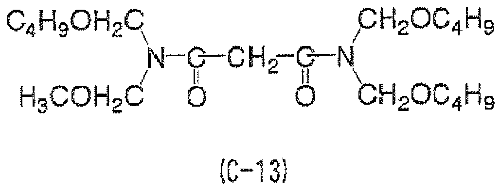


- As the compound having a hydroxymethyl group or an alkoxymethyl group, a compound represented by the following formula (I) or (II) is also preferred:

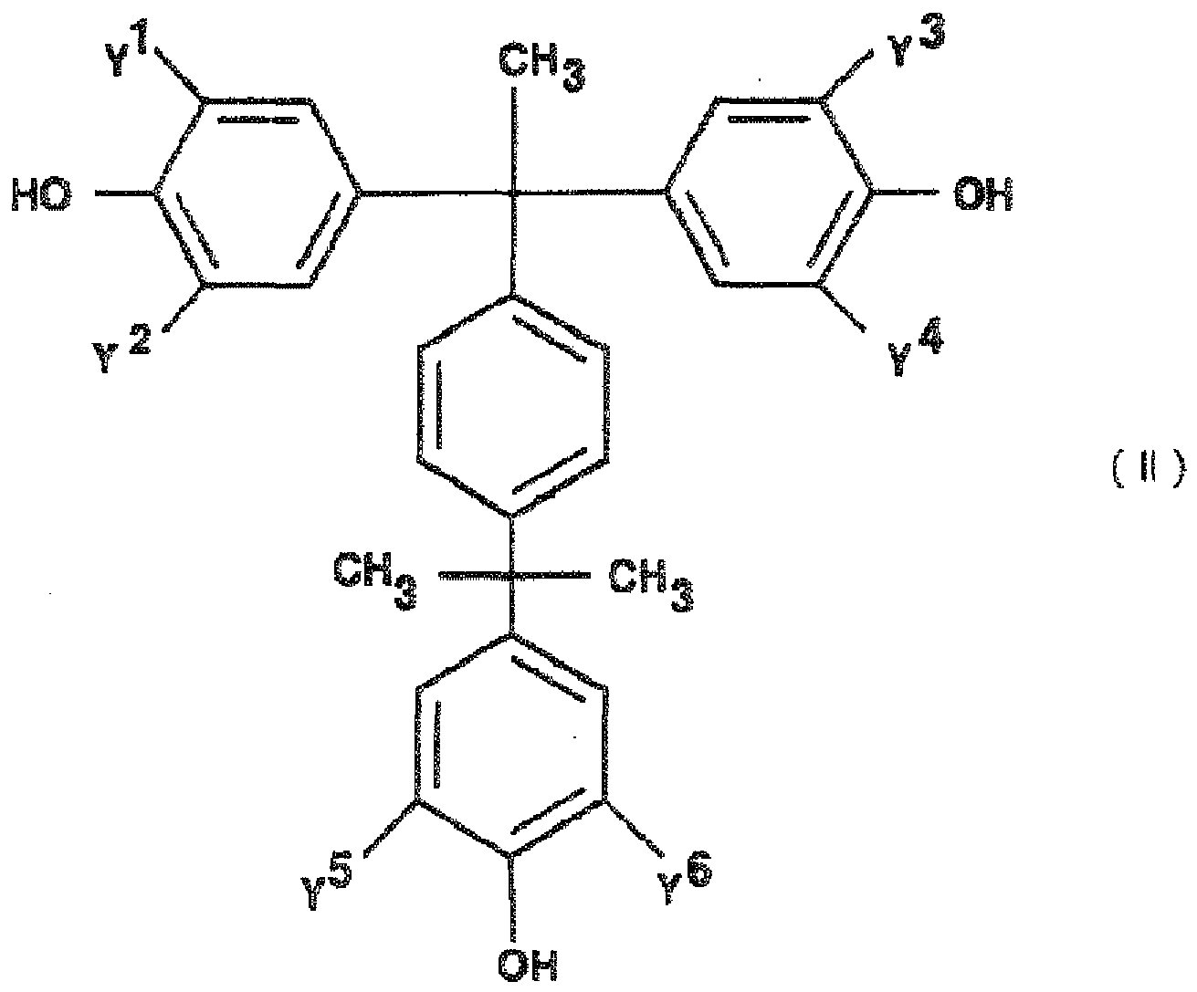
- In formula (I), each of X1 to X6 represents CH2OH or H, and at least three of X1 to X6 are CH2OH. In formula (II), each of Y1 to Y6 represents CH2OCH3, CH2OH or H, and at least three of Y1 to Y6 are CH2OCH3 or CH2OH, with at least one being CH2OCH3. Preferably, four or more of X1 to X6 are CH2OH, and four or more of Y1 to Y6 are CH2OCH3 or CH2OH, with at least one or more being CH2OCH3. More preferably, all of X1 to X6 are CH2OH, and all of Y1 to Y6 are CH2OCH3 or CH2OH, with at least one or more being CH2OCH3.
- The compound having an oxirane group is suitably an epoxy group having at least two epoxy groups per molecule, or an oxetane compound having at least two oxetanyl groups per molecule.
- Examples of the epoxy compound having at least two epoxy groups per molecule include, but are not limited to, a bixylenol-type or biphenol-type epoxy compound (such as "YX4000 produced by Japan Epoxy Resins Co., Ltd."), a mixture thereof, a heterocyclic epoxy compound having an isocyanurate skeleton or the like (such as "TEPIC produced by Nissan Chemicals Industries, Ltd." and "ARALDITE PT810 produced by BASF Japan"), a bisphenol A-type epoxy compound, a novolak-type epoxy compound, a bisphenol F-type epoxy compound (Epotohto YDF-170, produced by Tohto Kasei Co., Ltd.), a hydrogenated bisphenol A-type epoxy compound, a bisphenol S-type epoxy compound, a phenol novolak-type epoxy compound, a cresol novolak-type epoxy compound, a halogenated epoxy compound (such as low brominated epoxy compound, high halogenated epoxy compound and brominated phenol novolak-type epoxy compound), an allyl group-containing bisphenol A-type epoxy compound, a trisphenolmethane-type epoxy compound, a diphenyldimethanol-type epoxy compound, a phenol biphenylene-type epoxy compound, a dicyclopentadiene-type epoxy compound (such as "HP-7200, HP-7200H produced by DIC Corp."), a glycidylamine-type epoxy compound (such as diaminodiphenylmethane-type epoxy compound, glycidylaniline and triglycidylaminophenol), a glycidyl ester-type epoxy compound (such as diglycidyl phthalate, diglycidyl adipate, diglycidyl hexahydrophthalate and diglycidyl dimerate), a hydantoin-type epoxy compound, an alicyclic epoxy compound (such as 3,4-epoxycyclohexylmethyl-3',4'-epoxycyclohexanecarboxylate, bis(3,4-epoxycyclohexylmethyl)adipate, dicyclopentadiene diepoxide, and "GT-300, GT-400, EHPE3150 produced by Daicel Chemical Industries, Ltd."), an imide-type alicyclic epoxy compound, a trihydroxyphenylmethane-type epoxy compound, bisphenol A novolak-type epoxy compound, a tetraphenylolethane-type epoxy compound, a glycidyl phthalate compound, a tetraglycidyl xylenoylethane compound, a naphthalene group-containing epoxy compound (such as naphthol aralkyl-type epoxy compound, naphthol novolak-type epoxy compound, tetrafunctional naphthalene-type epoxy compound, and commercially available "ESN-190 and ESN-360 produced by Nippon Steel Chemical Co., Ltd.", and "HP-4032, EXA-4750 and EXA-4700 produced by DIC Corp."), a reaction product of epichlorohydrin with a polyphenol compound obtained by an addition reaction between a phenol compound and a diolefin compound such as divinylbenzene and dicyclopentadiene, a ring-opening polymerized 4-vinylcyclohexene-1-oxide epoxidized with peracetic acid or the like, an epoxy compound having a linear phosphorus-containing structure, an epoxy compound having a cyclic phosphorus-containing structure, an α-methylstilbene-type liquid crystal epoxy compound, a dibenzoyloxybenzene-type liquid crystal epoxy compound, an azophenyl-type liquid crystal epoxy compound, an azomethine phenyl-type liquid crystal epoxy compound, a binaphthyl-type liquid crystal epoxy compound, an azine-type epoxy compound, a glycidyl methacrylate copolymer-based epoxy compound (such as "CP-50S and CP-50M produced by NOF Corporation"), a copolymerized epoxy compound of cyclohexyl maleimide and glycidyl methacrylate, a bis(glycidyloxyphenyl)fluorene-type epoxy compound, and a bis(glycidyloxyphenyl)adamantane-type epoxy compound. One of these epoxy compounds may be used alone, or two or more thereof may be used in combination.
- Other than the epoxy compound having at least two epoxy groups per molecule, an epoxy compound containing, per molecule, at least two epoxy groups each having an alkyl group at the β-position may be used, and a compound containing an epoxy group substituted with an alkyl group at the β-position (more specifically, a β-alkyl-substituted glycidyl group or the like) is particularly preferred.
- In the epoxy compound containing at least an epoxy group having an alkyl group at the β-position, all of two or more epoxy groups contained per molecule may be a β-alkyl-substituted glycidyl group, or at least one epoxy group may be a β-alkyl-substituted glycidyl group.
- In the epoxy compound containing an epoxy group having has an alkyl group at the β-position, in view of storage stability at room temperature, the ratio of the β-alkyl-substituted glycidyl group in all epoxy groups is preferably 30 mol% or more, more preferably 40 mol% or more, still more preferably 50 mol% or more, based on the entire amount of the epoxy compound contained in the curable composition for a solid-state imaging device.
- The β-alkyl-substituted glycidyl group is not particularly limited and may be appropriately selected according to the purpose. Examples thereof include a β-methylglycidyl group, a β-ethylglycidyl group, a β-propylglycidyl group, and a β-butylglycidyl group. Among these, a β-methylglycidyl group is preferred from the standpoint of enhancing storage stability of the curable composition for a solid-state imaging device as well as in view of easy synthesis.
- The epoxy compound containing an epoxy group having an alkyl group at the β-position is preferably, for example, an epoxy compound derived from a polyhydric phenol compound and a β-alkylepihalohydrin.
- Moreover, the β-alkylepihalohydrin is not particularly limited and may be appropriately selected according to the purpose. Examples thereof include a β-methylepihalohydrin such as β-methylepichlorohydrin, β-methylepibromohydrin and β-methylepifluorohydrin; a β-ethylepihalohydrin such as β-ethylepichlorohydrin, β-ethylepibromohydrin and β-ethylepifluorohydrin; a β-propylepihalohydrin such as β-propylepichlorohydrin, β-propylepibromohydrin and β-propylepifluorohydrin; and a β-butylepihalohydrin such as β-butylepichlorohydrin, β-butylepibromohydrin and β-butylepifluorohydrin. Among these, β-methylepihalohydrin is preferred in view of reactivity with the polyhydric phenol and fluidity.
- The polyhydric phenol compound is not particularly limited as long as it is a compound containing two or more aromatic hydroxyl groups per molecule, and the compound may be appropriately selected according to the purpose. Examples thereof include a bisphenol compound such as bisphenol A, bisphenol F and bisphenol S, a biphenol compound such as biphenol and tetramethylbiphenol, a naphthol compound such as dihydroxynaphthalene and binaphthol, a phenol novolak compound such as phenol-formaldehyde polycondensate, a monoalkyl (having a carbon number of 1 to 10)-substituted phenol-formaldehyde polycondensate such as cresol-formaldehyde polycondensate, a dialkyl (having a carbon number of 1 to10)-substituted phenol-formaldehyde polycondensate such as xylenol-formaldehyde polycondensate, a bisphenol compound-formaldehyde polycondensate such as bisphenol A-formaldehyde polycondensate, a copolycondensate of phenol and a monoalkyl (having a carbon number of 1 to 10)-substituted phenol with formaldehyde, and a polyadduct of a phenol compound with divinylbenzene. Among these, for example, in the case of selecting the compound so as to improve the fluidity and storage stability, a bisphenol compound is preferred.
- Examples of the epoxy compound containing an epoxy group having an alkyl group at the β-position include a di-β-alkyl glycidyl ether of a bisphenol compound, such as di-β-alkyl glycidyl ether of bisphenol A, di-β-alkyl glycidyl ether of bisphenol F, and di-β-alkyl glycidyl ether of bisphenol S; a di-β-alkyl glycidyl ether of a biphenol compound, such as di-β-alkyl glycidyl ether of biphenol and di-β-alkyl glycidyl ether of tetramethyl biphenol; a β-alkyl glycidyl ether of a naphthol compound, such as di-β-alkyl glycidyl ether of dihydroxynaphthalene and di-β-alkyl glycidyl ether of binaphthol; a poly-β-alkyl glycidyl ether of a phenol-formaldehyde polycondensate; a poly-β-alkyl glycidyl ether of a monoalkyl (having a carbon number of 1 to 10)-substituted phenol-formaldehyde polycondensate, such as poly-β-alkyl glycidyl ether of cresol-formaldehyde polycondensate; a poly-β-alkyl glycidyl ether of a dialkyl (having a carbon number of 1 to 10)-substituted phenol-formaldehyde polycondensate, such as poly-β-alkyl glycidyl ether of xylenol-formaldehyde polycondensate; a poly-β-alkyl glycidyl ether of a bisphenol compound-formaldehyde polycondensate, such as poly-β-alkyl glycidyl ether of bisphenol A-formaldehyde polycondensate; and a poly-β-alkyl glycidyl ether of a polyadduct of a phenol compound with divinylbenzene.
- Among these, a β-alkyl glycidyl ether derived from a bisphenol compound represented by the following formula (D-1) and a polymer produced from the bisphenol compound and epichlorohydrin or the like, and a poly-β-alkyl glycidyl ether of a phenol compound-formaldehyde polycondensate represented by the following formula (D-2) are preferred:


- In formula (D-1), RD1 represents a hydrogen atom or an alkyl group having a carbon number of 1 to 6, and n represents an integer of 0 to 20.
- In formula (D-2), RD1 represents a hydrogen atom or an alkyl group having a carbon number of 1 to 6, RD2 represents a hydrogen atom or CH3, and n represents an integer of 0 to 20.
- In formulae (D-1) and (D-2), plurality of RD1 or RD2 are present, each of RD1 or RD2 may be the same as or different from every other RD1 or RD2.
- One of these epoxy compounds containing an epoxy group having an alkyl group at the β-position may be used alone, or two or more thereof may be used in combination. Also, an epoxy compound containing at least two epoxy rings per molecule and an epoxy compound containing an epoxy group having an alkyl group at the β-position may be used in combination.
- As for the skeleton of the epoxy compound, at least one compound selected from a bisphenol-type epoxy compound, a novolak-type epoxy compound, an alicyclic group-containing epoxy compound and a sparingly soluble epoxy compound is preferred.
- Examples of the oxetane compound containing at least two oxetanyl groups per molecule include polyfunctional oxetanes such as bis[(3-methyl-3-oxetanylmethoxy)methyl]ether, bis[(3-ethyl-3-oxetanylmethoxy)methyl]ether, 1,4-bis[(3-methyl-3-oxetanylmethoxy)methyl]benzene, 1,4-bis[(3-ethyl-3-oxetanylmethoxy)methyl]benzene, (3-methyl-3-oxetanyl)methyl acrylate, (3-ethyl-3-oxetanyl)methyl acrylate, (3-methyl-3-oxetanyl)methyl methacrylate, (3-ethyl-3-oxetanyl)methyl methacrylate, and an oligomer or a copolymer thereof; and an ether compound of a compound having an oxetane group with a resin having a hydroxyl group, such as novolak resin, poly(p-hydroxystyrene), cardo bisphenols, calixarenes, calixresorcinarenes and silsesquioxane. Other examples include a copolymer of an unsaturated monomer having an oxetane ring with an alkyl (meth)acrylate.
- The compound having a phenolic hydroxyl group includes a phenol resin such as novolak resin and resole resin. As the phenol resin, all known phenol resins can be used.
- As for the compound (C), a polyisocyanate compound described in
JP-A-5-9407 - Another example of the compound (C) includes a compound obtained by reacting a blocking agent with an isocyanate group of the polyisocyanate above or its derivative.
- Examples of the blocking agent for a isocyanate group include alcohols (e.g., isopropanol, tert-butanol), lactams (e.g., ε-caprolactam), phenols (e.g., phenol, cresol, p-tertbutylphenol, p-sec-butylphenol, p-sec-aminophenol, p-octylphenol, p-nonylphenol), heterocyclic hydroxyl compounds (e.g., 3-hydroxypyridine, 8-hydroxyquinoline), and active methylene compounds (e.g., dialkyl malonate, methyl ethyl ketoxime, acetylacetone, alkyl acetoacetate oxime, acetoxime, cyclohexanone oxime). In addition, for example, a compound having either at least one polymerizable double bond or at least one block isocyanate group within the molecule described in
JP-A-6-295060 - The compound (C) is preferably a low molecular compound having a molecular weight of 2,000 or less, more preferably a low molecular compound having a molecular weight of 1,500 or less, still more preferably a low molecular compound having a molecular weight of 900 or less. The low molecular compound as used in the present invention is not a so-called polymer or oligomer obtained by cleaving an unsaturated bond of a compound having an unsaturated bond (so-called polymerizable monomer) with use of an initiator, thereby growing the bond in a chain reaction, but indicates a compound having a certain molecular weight in a range of 2,000 or less (more preferably 1,500 or less, still more preferably 900 or less) (a compound substantially having no molecular weight distribution). Incidentally, the molecular weight is usually 100 or more.
- As the compound (C), one compound may be used alone, or two or more compounds may be used in combination.
- The content of the compound (C) is preferably from 1 to 50 mass%, more preferably from 3 to 30 mass%, based on the entire solid content by mass of the curable composition for a solid-state imaging device of the present invention.
- The curable composition for a solid-state imaging device of the present invention contains a binder resin.
- The binder resin is preferably an alkali-soluble binder. In this case, when exposure is performed to form a pattern in the film obtained from the curable composition, the unexposed area can be more reliably removed by an alkali developer, and a more excellent pattern can be formed by alkali development.
- The alkali-soluble binder contains an alkali-soluble group, and examples of the alkali-soluble group include an acid group, an alcoholic hydroxyl group, a pyrrolidone group, and an alkylene oxide group, with an acid group being preferred.
- The acid group is not particularly limited, but examples thereof include a carboxyl group, an active methylene group, a phosphonic acid group, a sulfonic acid group, a phenolic hydroxyl group, and a carboxylic anhydride group. Among these, a carboxyl group and an active methylene group are preferred, and a carboxyl group is more preferred.
- The alkali-soluble binder having an acid group is not particularly limited but is preferably a polymer obtained by using, as a monomer component, an acid group-containing polymerizable compound and from the standpoint of adjusting the acid value, a copolymer obtained by copolymerizing an acid group-containing polymerizable compound and an acid group-free polymerizable compound is more preferred.
- The acid group-containing polymerizable compound is not particularly limited and may be appropriately selected according to the purpose, and examples thereof include acrylic acid, methacrylic acid, itaconic acid, crotonic acid, isocrotonic acid, maleic acid, and p-carboxylstyrene, with acrylic acid, methacrylic acid and p-carboxylstyrene being preferred. One of these compounds may be used alone, or two or more thereof may be used in combination.
- The acid group-free polymerizable compound is not particularly limited, but preferred examples thereof include a (meth)acrylic acid ester (such as alkyl ester, aryl ester and aralkyl ester).
- The alkyl group in the alkyl ester moiety of the (meth)acrylic acid ester may be linear or branched and is preferably an alkyl group having a carbon number of 1 to 10, more preferably an alkyl group having a carbon number of 1 to 6.
- The aryl group in the aryl ester moiety of the (meth)acrylic acid ester is preferably an aryl group having a carbon number of 6 to 14, more preferably an aryl group having a carbon number of 6 to 10.
- The aralkyl group in the aralkyl ester moiety of the (meth)acrylic acid ester is preferably an aralkyl group having a carbon number of 7 to 20, more preferably an aralkyl group having a carbon number of 7 to 12.
- The molar ratio between a monomer corresponding to the acid group-containing polymerizable compound and a monomer corresponding to the acid group-free polymerizable compound is usually from 1:99 to 99:1, preferably from 30:70 to 99:1, more preferably from 50:50 to 99:1.
- The content of the acid group in the alkali-soluble binder is not particularly limited but is preferably from 0.4 to 4.0 meq/g, more preferably from 1.0 to 3.0 meq/g. When the content is 0.5 meq/g or more, satisfactory alkali developability is obtained and an excellent pattern can be more unfailingly obtained. Also, when the content is 4.0 meq/g or less, the fear of impairing the strength of the permanent pattern can be reliably avoided.
- A linear organic polymer is preferably used as the binder resin.
- The linear organic polymer is preferably a polymer having a carboxyl group in the side chain. Examples thereof include a methacrylic acid copolymer, an acrylic acid copolymer, an itaconic acid copolymer, a crotonic acid copolymer, a maleic acid copolymer and a partially esterified maleic acid copolymer described in
JP-A-59-44615 JP-B-54-34327 JP-B-58-12577 JP-B-54-25957 JP-A-59-53836 JP-A-59-71048 - Above all, a benzyl (meth)acrylate/(meth)acrylic acid copolymer, and a multicomponent copolymer composed of benzyl (meth)acrylate/(meth)acrylic acid/other monomers are preferred.
- In addition, for example, a polymer obtained by copolymerizing 2-hydroxyethyl methacrylate is also useful. The polymer may be used by mixing it in an arbitrary amount.
- As the specific constituent of the binder polymer, a copolymer of a (meth)acrylic acid and another monomer copolymerizable therewith is preferred. Here, the (meth)acrylic acid is a generic term which collectively encompasses acrylic acid and methacrylic acid, and hereinafter, (meth)acrylate is also a generic term of acrylate and methacrylate.
- Examples of another monomer copolymerizable with a (meth)acrylic acid include alkyl (meth)acrylates, aryl (meth)acrylates and a vinyl compound. Here, hydrogen atom of the alkyl group and the aryl group may be substituted with a substituent.
- Specific examples of the alkyl (meth)acrylate and the aryl (meth)acrylate include methyl (meth)acrylate, ethyl (meth)acrylate, propyl (meth)acrylate, butyl (meth)acrylate, isobutyl (meth)acrylate, pentyl (meth)acrylate, hexyl (meth)acrylate, octyl (meth)acrylate, phenyl (meth)acrylate, benzyl (meth)acrylate, tolyl (meth)acrylate, naphthyl (meth)acrylate and cyclohexyl (meth)acrylate.
- Examples of the vinyl compound include styrene, α-methylstyrene, vinyltoluene, glycidyl methacrylate, acrylonitrile, vinyl acetate, N-vinylpyrrolidone, tetrahydrofurfuryl methacrylate, polystyrene macromonomer, polymethyl methacrylate macromonomer, CH2=CR1R2, and CH2=C(R1)(COOR3) [wherein R1 represents a hydrogen atom or an alkyl group having a carbon number of 1 to 5, R2 represents an aromatic hydrocarbon ring having a carbon number of 6 to 10, and R3 represents an alkyl group having a carbon number of 1 to 8 or an aralkyl group having a carbon number of 6 to 12].
- One of these other copolymerizable monomers may be used alone, or two or more thereof may be used in combination. The another copolymerizable monomer is preferably at least one member selected from CH2=CR1R2, CH2=C(R1)(COOR3), phenyl (meth)acrylate, benzyl (meth)acrylate and styrene, more preferably CH2=CR1R2 and/or CH2=C(R1)(COOR3).
- The binder resin may be a resin having a crosslinking group, and in this case, a resin having a crosslinking group in the side chain is preferred. Thanks to such a configuration, particularly, both curability of the exposed area and alkali developability of the unexposed area can be enhanced.
- The crosslinking group as used herein indicates a group capable of crosslinking the binder resin in the process of a crosslinking reaction occurring in the photosensitive layer when the photosensitive layer obtained from the curable composition is exposed or heated.
- The crosslinking group is not particularly limited as long as it is a group having such a function, but examples of the crosslinking group include a phenol group, an ethylenically unsaturated bond group, an amino group, and an epoxy group. The ethylenically unsaturated bond group includes a styryl group, a (meth)acryloyl group or an allyl group, and from the standpoint of satisfying both stability of the crosslinking group before exposure and strength of the permanent pattern, a (meth)acryloyl group is preferred.
- The content of the crosslinking group in the binder resin is not particularly limited but is preferably from 0.3 to 3.0 meq/g, more preferably from 1.0 to 3.0 meq/g, still more preferably from 1.5 to 2.8 meq/g. When the content is 0.3 meq/g or more, the amount of curing reaction is sufficiently large and high sensitivity is obtained, and when the content is 3.0 meq/g or less, storage stability of the curable composition can be enhanced.
- The content (meg/g) above can be measured, for example, by iodine value titration.
- The crosslinking group-containing resin (hereinafter, sometimes referred to as specified binder resin A; the specified binder resin A is preferably an alkali-soluble binder) usable in the present invention preferably has, in its structure, an acid group for letting the resin become more unfailingly alkali-soluble and a crosslinking group, so as to enhance various performances such as removability of non-image area. The binder resin having such a partial structure is described in detail in
JP-A-2003-262958 - Examples of the binder resin having a crosslinking group are described below, but the binder resin is not limited thereto as long as an alkali-soluble group such as COOH group and OH group and a crosslinking group are contained in the molecule:
- (1) a urethane-modified polymerizable double bond-containing acrylic resin obtained by reacting a compound which has one unreacted isocyanate group remaining after previously reacting an isocyanate group and an OH group and contains at least one (meth)acryloyl group, with a carboxyl group-containing acrylic resin;
- (2) an unsaturated group-containing acrylic resin obtained by reacting a carboxyl group-containing acrylic resin with a compound having both an epoxy group and a polymerizable double bond within the molecule; and
- (3) a polymerizable double bond-containing acrylic resin obtained by reacting an OH group-containing acrylic resin with a dibasic acid anhydride having a polymerizable double bond.
- Among these, the resins of (1) and (2) are preferred.
- The crosslinking group-containing binder polymer usable in the present invention may be a binder polymer having at least one polymerizable group, such as a polymer having at least one ethylenically unsaturated double bond or an epoxy acrylate polymer.
- The polymer having at least one ethylenically unsaturated double bond preferably further has at least one acid group.
- The acid group includes those described above, but in view of raw material availability, a carboxyl group is preferred.
- As the crosslinking group in the specified binder resin A, for example, a (meth)acryl group such as (meth)acrylate group and (meth)acrylamide group, and various polymerizable double bonds such as vinyl ester, vinyl ether or allyl ether of carboxylic acid, can be used. Specific examples of the specified binder resin A include a compound obtained by adding a cyclic ether group-containing polymerizable compound such as glycidyl acrylate, glycidyl methacrylate and glycidyl ester of an unsaturated fatty acid (e.g., cinnamic acid), or an epoxy group-containing polymerizable compound such as compound having an alicylcic epoxy group (for example, having an epoxy group such as cyclohexene oxide in the same molecule) and a (meth)acryloyl group, to an acrylic resin containing a carboxyl group as the acid group. Other examples include a compound obtained by adding an isocyanate group-containing polymerizable compound such as isocyanatoethyl (meth)acrylate to an acrylic resin containing an acid group and a hydroxyl group; a compound obtained by adding a hydroxyl group-containing polymerizable compound such as hydroxyalkyl (meth)acrylate to an acrylic resin containing an anhydride group; and a compound obtained by copolymerizing a cyclic ether group-containing polymerizable compound such as glycidyl methacrylate with a vinyl monomer such as (meth)acryloyl alkyl ester and adding a (meth)acrylic acid to an epoxy group in the side chain.
- Examples of these compounds include those described in Japanese Patent
2,763,775 JP-A-3-172301 JP-A-2000-232264 - Among these, the specified binder resin A is preferably either one polymer compound selected from a compound obtained by adding a cyclic ether group (for example, a group having an epoxy group or an oxetane group in a partial structure)-containing polymerizable compound to a part of an acid group of a polymer compound, and a compound obtained by adding a carboxyl group-containing polymerizable compound to a part or all of cyclic ether groups of a polymer compound. At this time, the addition reaction between an acid group and a cyclic ether group-containing compound is preferably performed in the presence of a catalyst, and it is particularly preferred that the catalyst is selected from an acidic compound and a neutral compound.
- Above all, in view of development stability with aging of the curable composition for a solid-state imaging device, the specified binder resin A is preferably a polymer compound containing a carboxyl group in the side chain and at the same time, containing an aromatic group which may contain a heterocyclic ring, and an ethylenically unsaturated bond in the side chain.
- Examples of the aromatic group which may contain a heterocyclic ring (hereinafter, sometimes simply referred to as "aromatic group") include a benzene ring, a condensed ring formed by fusing 2 or 3 benzene rings, and a condensed ring formed by fusing a benzene ring and a 5-membered unsaturated ring.
- Specific examples of the aromatic group include a phenyl group, a naphthyl group, an anthryl group, a phenanthryl group, an indenyl group, an acenaphthenyl group, a fluorenyl group, a benzopyrrole ring group, a benzofuran ring group, a benzothiophene ring group, a pyrazole ring group, an isoxazole ring group, an isothiazole ring group, an indazole ring group, a benzisoxazole ring group, a benzisothiazole ring group, an imidazole ring group, an oxazole ring group, a thiazole ring group, a benzimidazole ring group, a benzoxazole ring group, a benzothiazole ring group, a pyridine ring group, a quinoline ring group, an isoquinoline ring group, a pyridazine ring group, a pyrimidine ring group, a pyrazine ring group, a phthalazine ring group, a quinazoline ring group, a quinoxaline ring group, an aciridine ring group, a phenanthridine ring group, a carbazole ring group, a purine ring group, a pyran ring group, a piperidine ring group, a piperazine ring group, an indole ring group, an indolizine ring group, a chromene ring group, a cinnoline ring group, an acridine ring group, a phenothiazine ring group, a tetrazole ring group, and a triazine ring group. Among these, a hydrocarbon aromatic group is preferred, and a phenyl group and a naphthyl group are more preferred.
- The aromatic group may have a substituent, and examples of the substituent include a halogen atom, an amino group which may have a substituent, an alkoxycarbonyl group, a hydroxyl group, an ether group, a thiol group, a thioether group, a silyl group, a nitro group, a cyano group, and alkyl, alkenyl, alkynyl, aryl group and heterocyclic groups each of which may have a substituent.
- The content of the acid group in the specified binder resin A is preferably from 1.0 to 4.0 meq/g, more preferably from 1.5 to 3.0 meq/g. When the content of the acid group is 1.0 meq/g or more, satisfactory alkali developability is obtained and an excellent pattern can be more unfailingly obtained. Also, when the content is 4.0 meq/g or less, the fear of impairing the strength of the permanent pattern can be reliably avoided.
- The preferred range of the content of the cross linking group in the specified binder resin A is the same as the preferred range described above for the content of the crosslinking group in the alkali-soluble binder.
- Another preferred example of the binder resin for use in the present invention is at least either one of a polyamide-based resin and a polyimide-based resin (hereinafter, sometimes referred to as specified binder resin B). The specified binder resin B includes, for example, a polyamide resin, a polyimide resin, a silicon-containing polyimide resin, a polyimidesiloxane resin, and a polymaleimide resin.
- The polyamide resin for use in the present invention includes a polyamide acid (polyamic acid), and the polyimide resin for use in the present invention is formed, for example, by thermal ring-closing imidization of the polyamic acid above as a precursor.
- The polyamic acid used for the synthesis of the polyamide resin and the polyimide resin usually contains a structural unit represented by the following formula (IV) as the main component:

- In formula (IV), n represents an integer of 0 to 4. R1 is an acid component residue and represents a trivalent or tetravalent organic group containing at least two carbon atoms.
- In view of heat resistance, R1 is preferably a trivalent or tetravalent group containing a cyclic hydrocarbon, an aromatic ring or an aromatic heterocyclic ring and having a carbon number of 6 to 30.
- Examples of the organic group represented by R1 include, but are not limited to, a group derived from a phenyl group, a biphenyl group, a terphenyl group, a naphthalene group, a perylene group, a diphenyl ether group, a diphenylsulfone group, a diphenylpropane group, a benzophenone group, a biphenyl trifluoropropane group, a cyclobutyl group, and a cyclopentyl group. Above all, R1 is preferably a phenyl group or a cyclobutyl group.
- R2 represents a divalent organic group containing at least two carbon atoms. In view of heat resistance, R2 is preferably a divalent group containing a cyclic hydrocarbon, an aromatic ring or an aromatic heterocyclic ring and having a carbon number of 6 to 30.
- Examples of the divalent organic group represented by R2 include, but are not limited to, a divalent group derived from a phenyl group, a biphenyl group, a terphenyl group, a naphthalene group, a perylene group, a diphenyl ether group, a diphenylsulfone group, a diphenylpropane group, a benzophenone group, a biphenyl trifluoropropane group, a diphenylmethane group, and a cyclohexylmethane group. Above all, R2 is preferably a diphenyl ether group, a diphenylsulfone group, a diphenylpropane group or a diphenylmethane group.
- The polymer containing a structural unit represented by formula (IV) as the main component may be a homopolymer containing only one structural unit represented by formula (IV) or a copolymer containing two or more structural units represented by formula (IV) differing from each other.
- Also, a structural unit other than the structural unit represented by formula (IV) may be contained as a copolymerization component.
- Still another preferred example of the binder resin for use in the present invention is a urethane resin (hereinafter, sometimes referred to as specified binder resin C). Here, the specified binder resin C may have a crosslinking group in the side chain.
- The crosslinking group which may be contained in the side chain of the specified binder resin C include a functional group represented by any one of the following formulae (C-1) to (C-3). The functional groups represented by formulae (C-1) to (C-3) are described below.

- In formula (C-1), each of R1 to R3 independently represents a hydrogen atom or a monovalent organic group. R1 is preferably a hydrogen atom or an alkyl group which may have a substituent, and because of high radical reactivity, more preferably a hydrogen atom or a methyl group. Also, each of R2 and R3 is independently, for example, a hydrogen, a halogen atom, an amino group, a carboxyl group, an alkoxycarbonyl group, a sulfo group, a nitro group, a cyano group, an alkyl group which may have a substituent, an aryl group which may have a substituent, an alkoxy group which may have a substituent, an aryloxy group which may have a substituent, an alkylamino group which may have a substituent, an arylamino group which may have a substituent, an alkylsulfonyl group which may have a substituent, or an arylsulfonyl group which may have a substituent, and because of high radical reactivity, preferably a hydrogen atom, a carboxyl group, an alkoxycarbonyl group, an alkyl group which may have a substituent, or an aryl group which may have a substituent.
- X represents an oxygen atom, a sulfur atom, or -N(R12)-, and R12 represents a hydrogen atom or a monovalent organic group. Here, R12 includes, for example, an alkyl group which may have a substituent, and because of high radical reactivity, is preferably a hydrogen atom, a methyl group, an ethyl group, or an isopropyl group.
- Examples of the substituent which can be introduced include an alkyl group, an alkenyl group, an alkynyl group, an aryl group, an alkoxy group, an aryloxy group, a halogen atom, an amino group, an alkylamino group, an arylamino group, a carboxyl group, an alkoxycarbonyl group, a sulfo group, a nitro group, a cyano group, an amido group, an alkylsulfonyl group, and an arylsulfonyl group.

- In formula (C-2), each of R4 to R8 independently represents a hydrogen atom or a monovalent organic group. Each of R4 to R8 is preferably, for example, a hydrogen atom, a halogen atom, an amino group, a dialkylamino group, a carboxyl group, an alkoxycarbonyl group, a sulfo group, a nitro group, a cyano group, an alkyl group which may have a substituent, an aryl group which may have a substituent, an alkoxy group which may have a substituent, an aryloxy group which may have a substituent, an alkylamino group which may have a substituent, an arylamino group which may have a substituent, an alkylsulfonyl group which may have a substituent, or an arylsulfonyl group which may have a substituent, and more preferably a hydrogen atom, a carboxyl group, an alkoxycarbonyl group, an alkyl group which may have a substituent, or an aryl group which may have a substituent.
- Examples of the substituent which can be introduced are the same as those described in formula (C-1). Y represents an oxygen atom, a sulfur atom, or -N(R12)-. R12 has the same meaning as R12 in formula (C-1) and the preferred examples are also the same.

- In formula (C-3), R9 is preferably, for example, a hydrogen atom or an alkyl group which may have a substituent, and because of high radical reactivity, more preferably a hydrogen atom or a methyl group. Each of R10 and R11 is independently, for example, a hydrogen atom, a halogen atom, an amino group, a dialkylamino group, a carboxyl group, an alkoxycarbonyl group, a sulfo group, a nitro group, a cyano group, an alkyl group which may have a substituent, an aryl group which may have a substituent, an alkoxy group which may have a substituent, an aryloxy group which may have a substituent, an alkylamino group which may have a substituent, an arylamino group which may have a substituent, an alkylsulfonyl group which may have a substituent, or an arylsulfonyl group which may have a substituent, and because of high radical reactivity, preferably a hydrogen atom, a carboxyl group, an alkoxycarbonyl group, an alkyl group which may have a substituent, or an aryl group which may have a substituent.
- Examples of the substituent which can be introduced are the same as those of the substituent which can be introduced in formula (C-1). Z represents an oxygen atom, a sulfur atom, -N(R13)-, or a phenylene group which may have a substituent. R13 is, for example, an alkyl group which may have a substituent, and because of high radical reactivity, preferably a methyl group, an ethyl group or an isopropyl group.
- The basic skeleton of the specified binder resin C for use in the present invention is described below.
- The specified binder resin C for use in the present invention is a polyurethane resin having, as the basic skeleton, a structural unit as a reaction product of at least one diisocyanate compound represented by the following formula (C-4) and at least one diol compound represented by formula (C-5):


- In formulae (C-4) and (C-5), each of X0 and Y0 independently represents a divalent organic residue.
- As long as at least either one of the diisocyanate compound represented by formula (C-4) and the diol compound represented by formula (C-5) has at least one of the groups represented by formulae (C-1) to (C-3), a polyurethane resin having introduced into the side chain thereof a group represented by formulae (C-1) to (C-3) is produced as a reaction product of the diisocyanate compound and the diol compound. According to such a method, a polyurethane resin having a crosslinking group in the side chain can be more easily produced than substitution on or introduction into the desired side chain after the reaction and production of the polyurethane resin.
- The diisocyanate compound represented by formula (C-4) includes, for example, a product obtained by an addition reaction of a triisocyanate compound with 1 equivalent of a crosslinking group-containing monofunctional alcohol or a monofunctional amine compound.
- Specific examples of the compound above for obtaining the diisocyanate compound are described in paragraphs [0034] to [0040] of
JP-A-2006-63550 - The diol compound represented by formula (C-5) widely includes, for example, a polyether diol compound, a polyester diol compound, and a polycarbonate diol compound.
- In the case where the specified binder resin C has a crosslinking group in the side chain, as the method for obtaining this specified binder resin C, a method where a diol compound having an unsaturated group in the side chain is used as a raw material for the production of a polyurethane resin, is also preferred, in addition to the above-described method. The diol compound may be, for example, a commercially available product such as trimethylolpropane monoallyl ether, or may be a compound easily produced by the reaction of a halogenated diol compound, a triol compound or an aminodiol compound with an unsaturated group-containing carboxylic acid, an acid chloride, an isocyanate, an alcohol, an amine, a thiol or an alkyl halide compound. Specific examples of such a compound include those described in paragraphs [0057] to [0066] of patent publication above, and the compounds described therein can be suitably used also in the present invention..
- In the synthesis of the specified binder resin C, in addition to the diol compound above, a diol compound having a carboxyl group may be also used in combination.
- Examples of this diol compound include those shown by formulae (17) to (19) in the patent publication above, and specific examples thereof include 3,5-dihydroxybenzoic acid, 2,2-bis(hydroxymethyl)propionic acid, 2,2-bis(2-hydroxyethyl)propionic acid, 2,2-bis(3-hydroxypropyl)propionic acid, bis(hydroxymethyl)acetic acid, bis(4-hydroxyphenyl)acetic acid, 2,2-bis(hydroxymethyl)butyric acid, 4,4-bis(4-hydroxyphenyl)pentanoic acid, tartaric acid, N,N-dihydroxyethylglycine, and N,N-bis(2-hydroxyethyl)-3-carboxy-propionamide.
- The presence of such a carboxyl group is preferred, because characteristics such as hydrogen bonding property and alkali solubility can be imparted to the specified binder resin C.
- The polyurethane resin having a crosslinking group in the side chain is more preferably a resin having a carboxyl group in the side chain. More specifically, a polyurethane resin containing, as equivalent, 0.3 meq/g or more, preferably from 0.35 to 1.50 meq/g, of an ethylenically unsaturated bond group in the side chain and at the same time, containing 0.4 meq/g or more, preferably from 0.45 to 1,00 meq/g, of a carboxyl group in the side chain is particularly preferred as the binder polymer for use in the present invention.
- The binder resin is preferably at least either one of a polyamide-based resin and a polyimide-based resin, more preferably a polyamide-based resin.
- The weight average molecular weight of the binder polymer which can be used in the curable composition for a solid-state imaging device of the present invention is preferably 3,000 or more, more preferably from 5,000 to 300,000, and most preferably from 10,000 to 30,000, and the number average molecular weight is preferably 1,000 or more, more preferably from 2,000 to 250,000. The polydispersity (weight average molecular weight/number average molecular weight) is preferably 1 or more, more preferably from 1.1 to 10.
- The binder resin may be any of a random polymer, a block polymer, a graft polymer and the like.
- The binder resin usable in the present invention can be synthesized by a conventionally known method. Examples of the solvent used at the synthesis include tetrahydrofuran, ethylene dichloride, cyclohexanone, propylene glycol monomethyl ether, propylene glycol monomethyl ether acetate, and butyl acetate. One of these solvents may be used alone, or two or more thereof may be mixed and used.
- The radical polymerization initiator used when the binder resin usable in the curable composition for a solid-state imaging device is synthesized from a vinyl bond-containing monomer, includes known compounds such as azo-based initiator and peroxide initiator.
- As the binder resin for use in the present invention, an acetal-modified polyvinyl alcohol-based binder resin having an acid group described, for example, in European Patents
993,966 1,204,000 andJP-A-2001-318463 - Other examples include a polymer compound having an acid group and an ethylenically unsaturated bond in the side chain and having a bisphenol A-type skeleton and a bisphenol F-type skeleton, a novolak resin having an acidic group and an ethylenically unsaturated bond, and a resol resin. These resins can be obtained by the technique described in paragraphs [0008] to [0027] of
JP-A-11-240930 - In addition, as the binder resin for use in the present invention, a resin obtained by adding an acid anhydride to a hydroxyl group-containing polymer, a polyhydroxystyrene-based resin, a polysiloxane-based resin, poly(2-hydroxyethyl (meth)acrylate), polyvinylpyrrolidone, polyethylene oxide, polyvinyl alcohol, and the like are also useful. The binder resin may be also a resin obtained by copolymerizing a monomer having hydrophilicity. Examples thereof include an alkoxyalkyl (meth)acrylate, a hydroxyalkyl (meth)acrylate, glycerol (meth)acrylate, a (meth)acrylamide, an N-methylolacrylamide, a secondary or tertiary alkylacrylamide, a dialkylaminoalkyl (meth)acrylate, a morpholine (meth)acrylate, an N-vinylpyrrolidone, an N-vinylcaprolactam, a vinylimidazole, a vinyl triazole, a methyl (meth)acrylate, an ethyl (meth)acrylate, a branched or linear propyl (meth)acrylate, a branched or linear butyl (meth)acrylate, and a phenoxyhydroxypropyl (meth)acrylate. As the monomer having hydrophilicity, for example, a monomer containing a tetrahydrofurfuryl group, a phosphoric acid group, a phosphoric acid ester group, a quaternary ammonium salt group, an ethyleneoxy chain, a propyleneoxy chain, a sulfonic acid group or a group derived from a salt thereof, or a morpholinoethyl group is useful.
- Moreover, the binder resin for use in the present invention not only can enhance the coating formability when applying the curable composition for a solder resist of a solid-state imaging device but also, by selecting the kind of the binder resin, can enhance the toughness or insulation reliability of the solder resist film formed. For example, when an epoxy acrylate-containing resin, a polyamide(imide)-containing resin, a polyimide precursor, a copolymer formed by containing a benzyl (meth)acrylate monomer and a (meth)acrylic acid monomer, or a copolymer formed by containing an allyl (meth)acrylate monomer and a (meth)acrylic acid is selected as the binder resin, strength of the cured film by exposure is improved and toughness and insulation reliability of the solder resist obtained by exposing and developing the curable composition for a solder resist of a solid-state imaging device are improved.
- The content of the binder resin is preferably from 5 to 80 mass%, more preferably from 10 to 70 mass%, based on the entire solid content by mass of the curable composition for a solid-state imaging device of the present invention.
- When the content is in this range, the exposure sensitivity is high, the processing time can be short, and good heat/cold shock resistance is obtained.
- The curing composition for a solid-state imaging device of the present invention may be dispersed using a known dispersant for the purpose of enhancing the dispersibility and dispersion stability of the infrared-blocking material in the curable composition.
- Examples of the dispersant usable in the present invention include a polymer dispersant (such as polyamide amine and a salt thereof, polycarboxylic acid and a salt thereof, high-molecular-weight unsaturated acid ester, modified polyurethane, modified polyester, modified poly(meth)acrylate, (meth)acrylic copolymer, and naphthalene sulfonic acid formalin condensate), and a surfactant such as polyoxyethylene alkylphosphate, polyoxyethylene alkylamine and alkanolamine.
- The polymer dispersant can be classified into a linear polymer, a terminal-modified polymer, a graft polymer, and a block polymer, by its structure.
- Examples of the terminal-modified polymer having an anchor moiety to the surface include a polymer having a phosphoric acid group at the terminal described in
JP-A-3-112992 JP-T-2003-533455 JP-A-2002-273191 JP-A-9-77994 JP-A-2008-29901 JP-A-2007-277514 - Examples of the graft polymer having an anchor moiety to the surface include a reaction product of a poly(lower alkyleneimine) and a polyester described in
JP-A-54-37082 JP-T-8-507960 JP-A-2009-258668 JP-A-9-169821 JP-A-2009-203462 JP-A-10-339949 JP-A-2004-37986 JP-A-2003-238837 JP-A-2008-9426 JP-A-2008-81732 JP-A-2010-106268 - As the macromonomer used when a graft polymer having an anchor moiety to surface is produced by radical polymerization, a known macromonomer can be used, and examples thereof include macromonomers AA-6 (polymethyl methacrylate in which the terminal group is methacryloyl group), AS-6 (polystyrene in which the terminal group is methacryloyl group), AN-6S (a copolymer of styrene and acrylonitrile, in which the terminal group is methacryloyl group), and AB-6 (polybutyl acrylate in which the terminal group is methacryloyl group) produced by Toagosei Co., Ltd.; PLACCEL FM5 (ε-caprolactone 5-mol equivalent adduct of 2-hydroxyethyl methacrylate), and FA10L (ε-caprolactone 10-mol equivalent adduct of 2-hydroxyethyl acrylate) produced by Daicel Chemical Industries; and a polyester-based macromonomer described in
JP-A-2-272009 JP-A-2-272009 - As the block polymer having an anchor moiety to surface, block polymers described in
JP-A-2003-49110 JP-A-2009-52010 - The dispersant used can be appropriately selected from, for example, know dispersants and surfactants.
- Specific examples thereof include "Disperbyk-101 (polyamidoamine phosphate), 107 (carboxylic acid ester), 110 (acid group-containing copolymer), 130 (polyamide), 161, 162, 163, 164, 165, 166 and 170 (high molecular copolymer)", and "BYK-P104, P105 (high-molecular-weight unsaturated polycarboxylic acid)" produced by BYK Chemie; "EFKA 4047, 4050-4010-4165 (polyurethane type), EFKA 4330-4340 (block copolymer), 4400-4402 (modified polyacrylate), 5010 (polyesteramide), 5765 (high-molecular-weight polycarboxylate), 6220 (fatty acid polyester), and 6745 (phthalocyanine derivative)" produced by EFKA; "AJISPER PB821, PB822, PB880 and PB881" produced by Ajinomoto-Fine-Techno Co., Inc.; "Florene TG-710 (urethane oligomer)" and "Polyflow No. 50E and No. 300 (acrylic copolymer)" produced by Kyoeisha Chemical Co., Ltd.; "Disparlon KS-860, 873SN, 874, #2150 (aliphatic polyvalent carboxylic acid), #7004 (polyether ester), DA-703-50, DA-705 and DA-725" produced by Kusumoto Chemicals Ltd.; "Demol RN, N (naphthalenesulfonic acid-formalin polycondensate), MS, C and SN-B (aromatic sulfonic acid-formalin polycondensate)", "Homogenol L-18 (polymer polycarboxylic acid)", "Emulgen 920, 930, 935 and 985 (polyoxyethylene nonylphenyl ether)" and "Acetamine 86 (stearylamine acetate)" produced by Kao Corporation; "Solsperse 5000 (phthalocyanine derivative), 13240 (polyesteramine), 3000, 17000, 27000 (polymer having a functional moiety at the terminal), 24000, 28000, 32000 and 38500 (graft-type polymer)" produced by The Lubrizol Corp.; "Nikkol T106 (polyoxyethylene sorbitan monooleate) and MYS-IEX (polyoxyethylene monostearate)" produced by Nikko Chemicals Co., Ltd.; T-8000E and the like produced by Kawaken Fine Chemicals, Ltd.; Organosiloxane Polymer KP341 produced by Shin-Etsu Chemical Co., Ltd.; "W001, cationic surfactant", nonionic surfactant such as polyoxyethylene lauryl ether, polyoxyethylene stearyl ether, polyoxyethylene oleyl ether, polyoxyethylene octyl phenyl ether, polyoxyethylene nonylphenyl ether, polyethylene glycol dilaurate, polyethylene glycol distearate, and sorbitan fatty acid ester, and anionic surfactant such as "W004, W005, and W017", produced by Yusho Co., Ltd.; "EFKA-46, EFKA-47, EFKA-47EA, EFKA POLYMER 100, EFKA POLYMER 400, EFKA POLYMER 401 and EFKA POLYMER 450" produced by Morishita Industries Co., Ltd.; polymer dispersant such as "Disperse Aid 6, Disperse Aid 8, Disperse Aid 15 and Disperse Aid 9100" produced by San Nopco Limited; "Adeka Pluronic L31, F38, L42, L44, L61, L64, F68, L72, P95, F77, P84, F87, P94, L101, P103, F108, L121, and P-123" produced by Adeka Corporation; and "Ionet (trade name) S-20" produced by Sanyo Chemical Industries, Ltd.
- One of these dispersants may be used alone, or two or more thereof may be used in combination. Also, the dispersant for use in the present invention may be used in combination with an alkali-soluble resin, together with the above-described terminal-modified polymer having an anchor moiety to the infrared-blocking material surface, graft polymer or block polymer. The alkali-soluble resin includes a (meth)acrylic acid copolymer, an itaconic acid copolymer, a crotonic acid copolymer, a maleic acid copolymer, a partially esterified maleic acid copolymer, an acidic cellulose derivative having a carboxylic acid in the side chain, and a resin obtained by modifying a hydroxyl group-containing polymer with an acid anhydride, with a (meth)acrylic acid copolymer being preferred. In addition, an N-position-substituted maleimide monomer copolymer described in
JP-A-10-300922 JP-A-2004-300204 JP-A-7-319161 - From the standpoint of dispersibility, developability and precipitation, the following resins described in
JP-A-2010-106268 - The dispersant resin described in
JP-A-2010-106268 - The dispersant is preferably a graft copolymer containing, in the molecule, a graft chain having a number of atoms, excluding hydrogen atom, of 40 to 10,000 and being selected from a polyester structure, a polyether structure and a polyacrylate structure, and preferably contains a structural unit represented by any one of the following formulae (1) to (4), more preferably a structural unit represented by any one of the following formulae (1A), (2A), (3) and (4):


- In formulae (1) to (4), each of X1, X2, X3, X4 and X5 independently represents a hydrogen atom or a monovalent organic group and in view of restriction in the synthesis, is preferably a hydrogen atom or an alkyl group having a carbon number of 1 to 12, more preferably a hydrogen atom or a methyl group, still more preferably a methyl group.
- In formulae (1) to (4), each of W1, W2, W3 and W4 independently represents an oxygen atom or NH and is preferably an oxygen atom.
- In formula (3), R' represents a branched or linear alkylene group (the carbon number is preferably from 1 to 10, more preferably 2 or 3) and is preferably a group represented by-CH2-CH(CH3)- or a group represented by -CH(CH3)-CH2-.
- In formulae (1) to (4), each of Y1, Y2, Y3 and Y4 independently represents a divalent linking group and is not particularly restricted in view of structure. Specific examples thereof include the following linking groups (Y-1) to (Y-20). In the structures below, A and B indicate bonds to the left terminal group and the right terminal group, respectively, in formulae (1) to (4). Among the structures shown below, in view of easy synthesis, (Y-2) and (Y-13) are preferred.


- In formulae (1) to (4), each of Z1, Z2, Z3 and Z4 independently represents a hydrogen atom or a monovalent substituent, and the structure of the substituent is not particularly limited. Specific examples thereof include an alkyl group, a hydroxyl group, an alkoxy group, an aryloxy group, a heteroaryloxy group, an alkylthloether group, an arylthioether group, a heteroarylthioether group and an amino group. Among these, from the standpoint of enhancing the dispersibility, those having a steric repulsion effect are preferred, and an alkyl group having a carbon number of 5 to 24 is preferred. Above all, a branched alkyl group having a carbon number of 5 to 24 or a cyclic alkyl group having a carbon number of 5 to 24 is preferred.
- In formulae (1) to (4), each of n, m, p and q represents an integer of 1 to 500.
- In formulae (1) and (2), each of j and k independently represents an integer of 2 to 8. In view of dispersion stability and developability, each of j and k in formulae (1) and (2) is preferably an integer of 4 to 6, and most preferably 5.
- In formula (4), R represents a hydrogen atom or a monovalent organic group and is not particularly limited in its structure but is preferably a hydrogen atom, an alkyl group, an aryl group or a heteroaryl group, more preferably a hydrogen atom or an alkyl group. When R is an alkyl group, the alkyl group is preferably a linear alkyl group having a carbon number of 1 to 20, a branched alkyl group having a carbon number of 3 to 20, or a cyclic alkyl group having a carbon number of 5 to 20, more preferably a linear alkyl group having a carbon number of 1 to 20, still more preferably a linear alkyl group having a carbon number of 1 to 6.
- As for R in formula (4), two or more R differing in the structure may be mixed and used in the specified resin.
- In view of dispersion stability and developability, the structural unit represented by formula (1) is preferably a structural unit represented by the following formula (1A).
- Also, in view of dispersion stability and developability, the structural unit represented by formula (2) is preferably a structural unit represented by the following formula (2A).

- In formula (1A), X1; Y1, Z1 and n have the same meanings as X1, Y1, Z1 and n in formula (1), and preferred ranges are also the same.
- In formula (2A), X2, Y2, Z2 and m have the same meanings as X2, Y2, Z2 and m in formula (2), and preferred ranges are also the same.
- Specific examples include the compounds illustrated below. In the compounds illustrated below, the numerical value attached to each structural unit (the numerical value attached to the repeating unit of the main chain) indicates the content [% by mass; shown as "At%"] of the structural unit. The numerical value attached to the repeating unit of the side chain indicates the number of repetitions of the repeating unit.


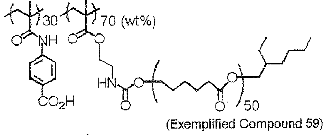


- In the case of using a dispersant, from the standpoint of enhancing the dispersibility, a dispersion composition is preferably prepared using the infrared-blocking material, a dispersant and an appropriate solvent and then blended in the curable composition.
- The curable composition for a solid-state imaging device of the present invention may or may not contain a dispersant, but in the case of containing a dispersant, the content thereof in the dispersion composition is preferably from 1 to 90 mass%, more preferably from 3 to 70 mass%, based on the entire solid content by mass of the infrared-blocking material in the dispersion composition.
- The curable composition for a solid-state imaging device of the present invention may contain a sensitizer for the purpose of enhancing the acid generation efficiency of the acid generator and shifting the photosensitive wavelength to a longer wavelength side. The sensitizer which can be used in the present invention is preferably a sensitizer capable of sensitizing the acid generator by an electron transfer mechanism or an energy transfer mechanism. The sensitizer usable in the present invention include those belonging to the compounds enumerated below and having an absorption wavelength in the wavelength region of 300 to 500 nm.
- Preferred examples of the sensitizer include those belonging to the following compounds and having an absorption wavelength in the region of 330 to 500 nm.
- Examples include polynuclear aromatics (e.g., phenanthrene, anthracene, pyrene, perylene, triphenylene, 9,10-dialkoxyanthracene), xanthenes (e.g., fluorescein, eosin, erythrosine, Rhodamine B, Rose Bengal), thioxanthones (isopropylthioxanthone, diethylthioxanthone, chlorothioxanthone), cyanines (e.g., thiacarbocyanine, oxacarbocyanine), merocyanines (e.g., merocyanine, carbomerocyanine), phthalocyanines, thiazines (e.g., thionine, methylene blue, toluidine blue), acridines (e.g., acridine orange, chloroflavin, acriflavin), anthraquinones (e.g., anthraquinone), squaryliums (e.g., squarylium), acridine orange, coumarins (e.g., 7-diethylamino-4-methylcoumarin), ketocoumarin, phenothiazines, phenazines, styryl benzenes, azo compounds, diphenylmethane, triphenylmethane, distyryl benzenes, carbazoles, porphyrin, spiro compounds, quinacridone, indigo, styryl, pyrylium compounds, pyromethene compounds, pyrazolotriazole compounds, benzothiazole compounds, barbituric acid derivatives, thiobarbituric acid derivatives, aromatic ketone compounds such as acetophenone, benzophenone, thioxanthone and Michler's ketone, and heterocyclic compounds such as N-aryl oxazolidinone.
- Examples further include compounds described in European Patent
568,993 U.S. Patents 4,508,811 and5,227,227 ,JP-A-2001-125255 JP-A-11-271969 - The curable composition for a solid-state imaging device may or may not contain a sensitizer but in the case of containing a sensitizer, the content thereof is preferably from 0.01 to 10 mass%, more preferably from 0.1 to 4 mass%, based on the entire solid content by mass of the curable composition for a solid-state imaging device of the present invention.
- The curable composition for a solid-state imaging device of the present invention may further contain a curing accelerator so as to accelerate curing of the above-described crosslinking agent.
- Examples of the curing accelerator which can be used include an amine compound (e.g., dicyandiamide, benzyldimethylamine, 4-(dimethylamino)-N,N-dimethylbenzylamine, 4-methoxy-N,N-dimethylbenzylamine, 4-methyl-N-,N-dimethylbenzylamine), a quaternary ammonium salt compound (e.g., triethylbenzylammonium chloride), a block isocyanate compound (e.g., dimethylamine), an imidazole derivative-bicyclic amidine compound and a salt thereof (e.g., imidazole, 2-methylimidazole, 2-ethylimidazole, 2-ethyl-4-methylimidazole, 2-phenylimidazole, 4-phenylimidazole, 1-cyanoethyl-2-phenylimidazole, 1-(2-cyanoethyl)-2-ethyl-4-methylimidazole), a phosphorus compound (e.g., triphenylphosphine), a guanamine compound (e.g., melamine, guanamine, acetoguanamine, benzoguanamine), and an S-triazine derivative (e.g., 2,4-diamino-6-methacryloyloxyethyl-S-triazine, 2-vinyl-2,4-diamino-S-triazine, 2-vinyl-4,6-diammo-S-triazine-isocyanuric acid adduct, 2,4-diamino-6-methacryloyloxyethyl-S-triazine-isocyanuric acid adduct). The curing accelerator is preferably melamine or dicyandiamine.
- One of these curing accelerators may be used alone, or two or more thereof may be used in combination.
- The curable composition for a solid-state imaging device may or may not contain a curing accelerator, but in the case of containing a curing accelerator, the content thereof is usually from 0.01 to 15 mass% based on the entire solid content of the curable composition.
- The curable composition for a solid-state imaging device of the present invention may further contain a filler. The filler which can be used in the present invention includes spherical silica surface-treated with a silane coupling agent.
- The curable composition of the present preferably contains a filler, because a pattern having high durability is obtained (in particular, when higher durability is required of the solder resist, for example, when the wiring density of metal wiring covered with the solder resist is high, the above-described effect is prominent).
- By using spherical silica surface-treated with a silane coupling agent, the thermal cycle test resistance and storage stability of the curable composition are enhanced, and the same good profile as that immediately after pattern formation can be maintained, for example, even through a harsh atmosphere such as thermal cycle test.
- The term "spherical" in the spherical filler may be sufficient if the particle is not of a needle-like, columnar or amorphous shape but is rounded, and the shape need not be necessarily "truly spherical". However, the typical "spherical" form is "a truly spherical" shape.
- Whether the filler is spherical can be confirmed by observing it though a scanning electron microscope (SEM).
- The volume average primary particle diameter of the filler is not particularly limited and may be appropriately selected according to the purpose but is preferably from 0.05 to 3 µm, more preferably from 0.1 to 1 µm. When the volume average primary particle diameter of the filler is in the range above, this is advantageous in that impairment of the processability due to development of thixotropy is suppressed and the maximum particle diameter is kept from becoming large, as a result, generation of a defect attributable to attachment of an extraneous material to the cured film obtained or non-uniformity of the coating film can be reduced.
- The volume average primary particle diameter of the filler can be measured by a dynamic light scattering particle diameter distribution measuring apparatus.
- The filler can be dispersed using the above-described dispersant and binder. As stated earlier, in view of curability, a resin (preferably an alkali-soluble binder) having a crosslinking group in the side chain is preferred.
- The surface treatment of the filler is described below. The surface treatment of the filler is not particularly limited and may be appropriately selected according to the purpose, but a treatment of covering silica with a silane coupling agent is preferred.
- The silane coupling agent used for the surface treatment of the filler is not particularly limited and may be appropriately selected according to the purpose but preferably contains at least one functional group selected from an alkoxysilyl group, a chlorosilyl group and an acetoxysilyl group (hereinafter, sometimes referred to as "first functional group") and at least one functional group selected from a (meth)acryloyl group, an amino group and an epoxy group (hereinafter, sometimes referred to as "second functional group). The second functional group is more preferably a (meth)acryloyl group or an amino group, and it is still more preferred that the second functional group is a (meth)acryloyl group. When the second functional group is a (meth)acryloyl group, this is advantageous in view of storage stability and TCT resistance.
- A silane coupling agent containing, as a first functional group, at least one member selected from an alkoxysilyl group, a chlorosilyl group and an acetoxysilyl group and, as a second functional group, at least one member selected from an imidazole group, an alkylimidazole group and a vinylimidazole group, described in
JP-B-7-68256 - The silane coupling agent is not particularly limited, but preferred examples thereof include a γ-aminopropyltriethoxysilane, N-(β-aminoethyl)-γ-aminopropyltrimethoxysilane, N-(β-aminoethyl)-γ-aminopropylmethyldimethoxysilane, γ-glycidoxypropyltrimethoxysilane, γ-glycidoxypropylmethyldimethoxysilane, γ-methacryloxypropyltriethoxysilane, γ-methacryloxypropylmethyldimethoxysilane, α-[[3-(trimethoxysilyl)propoxy]methyl]-imidazole-1-ethanol described in
JP-B-7-68256 - The surface treatment of spherical silica with the silane coupling agent may be previously performed only for the spherical silica (in this case, hereinafter, sometimes referred to as "pretreatment") or may be performed together with a part or all of other fillers contained in the curable composition.
- The method for performing the pretreatment is not particularly limited, and examples of the method include a dry method, an aqueous solution method, an organic solvent method and a spray method. The temperature at which the pretreatment is performed is not particularly limited but is preferably from ordinary temperature to 200°C.
- It is also preferred to add a catalyst when performing the pretreatment. The catalyst is not particularly limited, and examples thereof include an acid, a base, a metal compound, and an organic metal compound.
- In the case of performing the pretreatment, the amount of the silane coupling agent added is not particularly limited but is preferably from 0.01 to 50 parts by mass, more preferably from 0.05 to 50 parts by mass, per 100 parts by mass of the spherical silica. When the amount added is in this range, a surface treatment enough to develop the effect is performed and at the same time, impairment of the handleability due to aggregation of spherical silica after treatment is reduced.
- The above-described silane coupling agent has an action of enhancing the adherence between the base material and the photosensitive layer, because the first functional group reacts with an active group in the base material surface, spherical silica surface and binder and the second functional group reacts with a carboxyl group and an ethylenically unsaturated group of the binder. On the other hand, the silane coupling agent has high reactivity and if the silane coupling agent itself is added to the curable composition, mainly the second functional group sometimes undergoes reaction or deactivation during storage due to its diffusion action, leading to reduction in the shelf life or pot life.
- However, when spherical silica pretreated with a silane coupling agent is used, the diffusion action is suppressed and the problem of shelf life or pot life is greatly improved, making it possible to take even a one-component system. Furthermore, in the case of applying the pretreatment to spherical silica, the conditions such as stirring condition, temperature condition and use of catalyst can be freely selected, so that compared to the addition without performing the pretreatment, the reaction ratio of the first functional group of the silane coupling agent with an active group in the spherical silica can be significantly increased. Accordingly, very good results are obtained in terms of required characteristics under harsh conditions such as electroless gold plating, electroless solder plating and moisture resistance load test. Also, by performing the pretreatment, the amount of the silane coupling agent used can be decreased, and the shelf life and pot life can be more improved.
- Examples of the spherical silica surface-treated with a silane coupling agent, which can be used in the present invention, include FB and SFP Series of Denki Kagaku Kogyo Kabushiki Kaisha; 1-FX of Tatsumori Ltd.; HSP Series of Toagosei Co., Ltd.; and SP Series of Fuso Chemical Co., Ltd.
- The curable composition for a solid-state imaging device of the present invention may or may not contain a filler, but in the case of containing a filler, the content thereof based on the entire solid content by mass of the curable composition is not particularly limited and may be appropriately selected according to the purpose, and the content is preferably from 1 to 60 mass%. When the amount added is in this range, sufficient reduction in the linear expansion coefficient is achieved and at the same time, the cured film formed can be kept from embrittlement, as a result, when wiring is formed using a permanent pattern, the function as a protective film for the wiring is adequately exerted.
- The curable composition for a solid-state imaging device of the present invention may further contain an elastomer.
- By containing an elastomer, the adherence to the conductive layer of a printed wiring board when using the curable composition for a solder resist can be more improved and at the same time, heat resistance, thermal shock resistance, flexibility and toughness of the cured film can be more enhanced.
- The elastomer which can be used in the present invention is not particularly limited and may be appropriately selected according to the purpose, and examples thereof include a styrene-based elastomer, an olefin-based elastomer, a urethane-based elastomer, a polyester-based elastomer, a polyamide-based elastomer, an acrylic elastomer, and a silicone-based elastomer. Such an elastomer is composed of a hard segment component and a soft segment component, where in general, the former contributes to heat resistance and strength and the latter contributes to flexibility and toughness. Among these, a polyester-based elastomer is advantageous in view of compatibility with other materials.
- Examples of the styrene-based elastomer include a styrene-butadiene-styrene block copolymer, a styrene-isoprene-styrene block copolymer, a styrene-ethylene-butylene-styrene block copolymer, and a styrene-ethylene-propylene-styrene block copolymer. As the component constituting the styrene-based elastomer, other than styrene, a styrene derivative such as α-methylstyrene, 3-methylstyrene, 4-propylstyrene and 4-cyclohexylstyrene can be used. Specific examples thereof include TUFPRENE, SOLPRENE T, ASAPRENE T, Tuftec (all produced by Asahi Kasei Corporation), Elastomer AR (produced by Aronkasei Co., Ltd.), Kraton G, Califlex (both produced by Shell in Japan), JSR-TR, TSR-SIS, Dynaron (all produced by JSR), Denka STR (produced Denki Kagaku Kogyo K.K.), Quintac (produced by ZEON Corporation), TPE-SB Series (produced by Sumitomo Chemical Co., Ltd.), Rabalon (produced by Mitsubishi Chemical Corporation), Septon, HYBRAR (both produced by Kuraray Co., Ltd.), Sumiflex (produced by Sumitomo Bakelite Co., Ltd.), Leostomer, and Actymer (both produced by Riken Vinyl Industry Co., Ltd.).
- The olefin-based elastomer is a copolymer of α-olefin having a carbon number of 2 to 20, such as ethylene, propylene, 1-butene, 1-hexene and 4-methyl-pentene, and examples thereof include an ethylene-propylene copolymer (EPR) and an ethylene-propylene-diene copolymer (EPDM). Also, the olefm-based elastomer includes, for example, a copolymer of an α-olefin and a nonconjugated diene having a carbon number of 2 to 20, such as dicyclopentadiene, 1,4-hexadiene, cyclooctadiene, methylenenorbornene, ethylidenenorbornene, butadiene and isoprene, and an epoxidized polybutadiene. The olefin-based elastomer further includes, for example, carboxyl-modified NBR obtained by copolymerizing methacrylic acid with a butadiene-acrylonitrile copolymer. Other examples of the olefin-based elastomer include an ethylene-α-olefin copolymer rubber, an ethylene-α-olefin-nonconjugated diene copolymer rubber, a propylene-α-olefin copolymer rubber, and a butene-α-olefin copolymer rubber.
- Specific examples of the olefin-based elastomer include Milastomer (produced by Mitsui Petrochemical Industries, Ltd.), EXACT (produced by Exxon Chemical), ENGAGE (produced by Dow Chemical), hydrogenated styrene-butadiene rubber "DYNABON HSBR" (produced by JSR), butadiene-acrylonitrile copolymer "NBR Series" (produced by JSR), butadiene-acrylonitrile copolymer modified at both ends with a carboxyl group having a crosslinking site "XER Series" (produced by JSR), and epoxidized polybutadiene obtained by partially epoxidizing polybutadiene "BF-1000" (produced by Nippon Soda Co., Ltd.).
- The urethane-based elastomer consists of structural units, that is, a hard segment composed of low molecular (short chain) diol and diisocyanate, and a soft segment composed of polymer (long chain) diol and diisocyanate. Examples of the polymer (long chain) diol include polypropylene glycol, polytetramethylene oxide, poly(1,4-butylene adipate), poly(ethylene-1,4-butylene adipate), polycaprolactone, poly(1,6-hexylene carbonate), and poly(1,6-hexylene-neopentylene adipate). The number average molecular weight of the polymer (long chain) diol is preferably from 500 to 10,000. Examples of the low molecular (short chain) diol include ethylene glycol, propylene glycol, 1,4-butanediol, and bisphenol A. The number average molecular weight of the short chain diol has is preferably from 48 to 500. Specific examples of the urethane-based elastomer include PANDEX T-2185 and T-2983N (both produced by DIC Corporation), and Shirakutoran E790.
- The polyester-based elastomer is obtained by polycondensing a dicarboxylic acid or a derivative thereof and a diol compound or a derivative thereof. Specific examples of the dicarboxylic acid include an aromatic dicarboxylic acid such as terephthalic acid, isophthalic acid and naphthalenedicarboxylic acid; an aromatic dicarboxylic acid where a hydrogen atom of the above-described aromatic ring is substituted with a methyl group, an ethyl group, a phenyl group or the like; an aliphatic dicarboxylic acids having a carbon number of 2 to 20, such as adipic acid, sebacic acid and dodecanedicarboxylic acid; and an alicyclic dicarboxylic acid such as cyclohexanedicarboxylic acid. One of these compounds or two or more thereof may be used. Specific examples of the diol compound include an aliphatic or alicyclic diol such as ethylene glycol, 1,3-propanediol, 1,4-butanediol, 1,6-hexanediol, 1,10-decanediol and 1,4-cyclohexanediol, bisphenol A, bis-(4-hydroxyphenyl)-methane, bis-(4-hydroxy-3-methylphenyl)-propane, and resorcin. One of these compounds or two or more thereof may be used. A multi-block copolymer using an aromatic polyester (e.g. polybutylene terephthalate) moiety for the hard segment component and an aliphatic polyester (e.g. polytetramethylene glycol) moiety for the soft segment component, can be used. The polyester-based elastomer includes various grades according to the kind, ratio and difference in the molecular weight of the hard segment and the soft segment. Specific examples of the polyester-based elastomer include Hytrel (produced by Du Pont-Toray Co., Ltd.), PELPRENE (produced by Toyobo Co., Ltd.), and ESPEL (produced by Hitachi Chemical Co., Ltd.).
- The polyamide-based elastomer consists of a hard segment composed of polyamide and a soft segment composed of polyether or polyester and is roughly classified into two types, that is, a polyether block amide type and a polyether ester block type. Examples of the polyamide include polyamide-6, polyamide-11, and polyamide-12. Examples of the polyether include polyoxyethylene, polyoxypropylene, and polytetramethylene glycol. Specific examples of the polyamide-based elastomer include UBE Polyamide Elastomer (produced by Ube Industries, Ltd.), DAIAMID (produced by Daicel-Huels), PEBAX (produced by Toray Industries, Inc.), Grilon ELY (EMS Japan), Novamid (produced by Mitsubishi Chemical Corporation), and Grilax (produced by DIC Corporation).
- The acrylic elastomer is obtained by copolymerizing an acrylic acid ester such as ethyl acrylate, butyl acrylate, methoxyethyl acrylate and ethoxyethyl acrylate, an epoxy group-containing monomer such as glycidyl methacrylate and alkyl glycidyl ether, and/or a vinyl-based monomer such as acrylonitrile and ethylene. Examples of the acrylic elastomer include an acrylonitrile-butyl acrylate copolymer, an acrylonitrile-butyl acrylate-ethyl acrylate copolymer, and an acrylonitrile-butyl acrylate-glycidyl methacrylate copolymer.
- The silicone-based elastomer is mainly composed of an organopolysiloxane and can be classified into a polydimethylsiloxane type, a polymethylphenylsiloxane type and a polydiphenylsiloxane type. An organopolysiloxane partially modified with a vinyl group, an alkoxy group or the like may be also used. Specific examples of the silicone-based elastomer include KE Series (produced by Shin-Etsu Chemical Co., Ltd.), SE Series, CY Series and SH Series (all produced by Dow Corning Toray Silicone Co., Ltd.).
- Other than the elastomers described above, a rubber-modified epoxy resin may be used. The rubber-modified epoxy resin is obtained by modifying a part or all of epoxy groups in the above-described bisphenol F-type epoxy resin, bisphenol A-type epoxy resin, salicylaldehyde-type epoxy resin, phenol novolak-type epoxy resin, cresol novolak-type epoxy resin or the like with, for example, a both-terminal carboxylic acid-modified butadiene-acrylonitrile rubber or a terminal amino-modified silicone rubber.
- Among the elastomers, in view of shear adherence and thermal shock resistance, a both-terminal carboxyl group-modified butadiene-acrylonitrile copolymer, and ESPEL that is a polyester-based elastomer having a hydroxyl group (ESPEL 1612 and 1620, produced by Hitachi Chemical Co., Ltd.), and epoxidized polybutadiene are preferred.
- The curable composition for a solid-state imaging device of the present invention may or may not contain an elastomer, but in the case of containing an elastomer, the content thereof based on the entire solid content by mass of the curable composition is not particularly limited and may be appropriately selected according to the purpose. The content is preferably from 0.5 to 30 mass%, more preferably from 1 to 10 mass%, still more preferably from 3 to 8 mass%, based on the solid content. When the content is in this preferred range, the shear adherence and thermal shock resistance can be advantageously more enhanced.
- From the standpoint of more enhancing the coatability, in the curable composition for a solid-state imaging device of the present invention, various surfactants may be added. As the surfactant, a variety of surfactants such as fluorine-containing surfactant, nonionic surfactant, cationic surfactant, anionic surfactant and silicone-containing surfactant may be used.
- In particular, when the curable composition for a solid-state imaging device of the present invention contains a fluorine-containing surfactant, the liquid characteristics (particularly, fluidity) of a coating solution prepared can be more enhanced and therefore, uniformity of the coating thickness and liquid saving performance can be more improved.
- That is, in the case of forming a film by using a coating solution to which a curable composition for a solid-state imaging device containing a fluorine-containing surfactant is applied, the interfacial tension between the surface to be coated and the coating solution is lowered, whereby wettability of the surface to be coated is improved and coatability on the surface to be coated is enhanced. This is effective in that even when a thin film on the order of several µm is formed with a small amount of solution, a film being reduced in the thickness unevenness and having a uniform thickness can be more successfully performed.
- The fluorine content of the fluorine-containing surfactant is preferably from 3 to 40 mass%, more preferably from 5 to 30 mass%, still more preferably from 7 to 25 mass%. The fluorine-containing surfactant having a fluorine content in this range is effective in view of thickness uniformity of the coated film or liquid saving performance and also exhibits good solubility in the curable composition for a solid-state imaging device.
- Examples of the fluorine-containing surfactant include Megaface F171, Megaface F172, Megaface F173, Megaface F176, Megaface F177, Megaface F141, Megaface F142, Megaface F143, Megaface F144, Megaface R30, Megaface F437, Megaface F475, Megaface F479, Megaface F482, Megaface F554, Megaface F780, Megaface F781 (all produced by DIC Corporation), Fluorad FC430, Fluorad FC431, Fluorad FC171 (all produced by Sumitomo 3M Ltd.), Surflon S-382, Surflon SC-101, Surflon SC-103, Surflon SC-104, Surflon SC-105, Surflon SC-1068, Surflon SC-381, Surflon SC-383, Surflon S-393, and Surflon KH-40 (all produced by Asahi Glass Co., Ltd.).
- Specific examples of the nonionic surfactant include polyoxyethylene lauryl ether, polyoxyethylene stearyl ether, polyoxyethylene oleyl ether, polyoxyethylene octylphenyl ether, polyoxyethylene nonylphenyl ether, polyethylene glycol dilaurate, polyethylene glycol distearate, and a sorbitan fatty acid ester (Pluronic L10, L31, L61, L62, 10R5, 17R2 and 25R2, and Tetronic 304, 701, 704, 901, 904 and 150R1, produced by BASF), and Solsperse 20000 (produced by The Lubrizol Corporation)).
- Specific examples of the cationic surfactant include a phthalocyanine derivative (EFKA-745, trade name, produced by Morishita Sangyo K.K.), organosiloxane polymer KP341 (produced by Shin-Etsu Chemical Co., Ltd.), (meth)acrylic acid (co)polymers POLYFLOW No. 75, No. 90 and No. 95 (produced by Kyoeisha Chemical Co., Ltd.), and W001 (produced by Yusho Co., Ltd.).
- Specific examples of the anionic surfactant include W004, W005 and W017 (produced by Yusho Co Ltd.).
- Examples of the silicone-containing surfactant include "TORAY SILICONE DC3PA", "TORAY SILICONE SH7PA", "TORAY SILICONE DC11PA", "TORAY SILICONE SH21PA", "TORAY SILICONE SH28PA", "TORAY SILICONE SH29PA", "TORAY SILICONE SH30PA" and "TORAY SILICONE SH8400" produced Dow Coming Toray Silicone Co., Ltd.; "TSF-4440", "TSF-4300", "TSF-4445", "TSF-4460" and "TSF-4452" produced by Momentive Performance Materials Inc.; "KP341", "KF6001" and "KF6002" produced by Shin-Etsu Silicone; and "BYK-323" and "BYK-330" produced by BYK Chemie.
- As the surfactant, one kind of a surfactant may be used, or two or more kinds of surfactants may be used in combination.
- The curable composition for a solid-state imaging device may or may not contain a surfactant, but in the case of containing a surfactant, the content thereof is preferably from 0.001 to 1 mass%, more preferably from 0.01 to 0.1 mass%, based on the entire solid content by mass of the curable composition of the present invention.
- In the curable composition for a solid-state imaging device of the present invention, in addition to the above-described essential components and preferred additives, other components may be appropriately selected and used according to the purpose as long as the effects of the present invention are not impaired.
- Examples of other components which can be used in combination include a heat curing accelerator, a thermal polymerization inhibitor, a plasticizer, and a colorant (colored pigment or dye). Furthermore, an adherence promoter to the base material and other auxiliary agents (for example, an electrically conductive particle, a filler, a defoaming agent, a flame retardant, a leveling agent, a release promoter, an antioxidant, a perfume, a surface tension adjusting agent and a chain transfer agent) may be also used in combination.
- By appropriately incorporating these components, the properties of the solder resist, such as stability, photographic property and film property, can be adjusted in a targeted manner.
- The thermal polymerization inhibitor is described in detail, for example, in paragraphs [0101] and [0102] of
JP-A-2008-250074 - The plasticizer is described in detail, for example, in paragraphs [0103] and [0104] of
JP-A-2008-250074 - The colorant is described in detail, for example, in paragraphs [0105] and [0106] of
JP-A-2008-250074 JP-A-2009-205029 - The adherence promoter is described in detail, for example, in paragraphs [0107] to [0109] of
JP-A-2008-250074 - All of the additives described in these patent publications are usable for the curable composition for a solid-state imaging device of the present invention.
- The solid content concentration of the thus-obtained curable composition for a solid-state imaging device of the present invention is preferably from 5 to 90 mass%, more preferably from 20 to 80 mass%, and most preferably from 40 to 60 mass%.
- The use application of the curable composition for a solid-state imaging device of the present invention is not particularly limited, but examples thereof include a solder resist, a light-blocking film for back surface of a silicon substrate in a solid-state imaging device, and a light-blocking film for wafer-level lens, with a solder resist being preferred.
- In the case where the curable composition for a solid-state imaging device of the present invention is used for a solder resist, in order to form a coating film having a relatively large thickness, the solid content concentration is preferably from 30 to 80 mass%, more preferably from 35 to 70 mass%, and most preferably from 40 to 60 mass%.
- The viscosity of the curable composition for a solid-state imaging device of the present invention is preferably from 1 to 3,000 mPa•s, more preferably from 10 to 1,500 mPa•s, and most preferably from 200 to 1,000 mPa•s.
- As for the method to obtain the desired viscosity, for example, a liquid dispersion prepared by dispersing at least either one of a filler and an elastomer is previously adjusted to a viscosity of 100 to 60,000 mPa•s, and other components are added thereto, whereby a curable composition for a solid-state imaging device having a desired viscosity can be obtained.
- The present invention also relates to a photosensitive layer formed of the curable composition for a solid-state imaging device of the present invention. Since the photosensitive layer is formed of the curable composition for a solid-state imaging device of the present invention, this is a photosensitive layer capable of forming a pattern having high light-blocking effect in the infrared region and excellent durability (for example, heat/cold shock resistance and adherence to substrate) as well as having a desired rectangular profile, by alkali development.
- The present invention also relates to a permanent pattern formed using the curable composition for a solid-state imaging device of the present invention. The permanent pattern of the present invention is obtained by applying exposure and alkali development to the photosensitive layer formed of the curable composition for a solid-state imaging device of the present invention and thanks to use of the curable composition for a solid-state imaging device of the present invention, the pattern formed by alkali development is a pattern having high light-blocking effect in the infrared region and excellent durability (for example, heat/cold shock resistance and adherence to substrate) as well as having a desired rectangular profile.
- Furthermore, the present invention also relates to a pattern forming method comprising, in order, a step of forming a photosensitive layer by using the curable composition for a solid-state imaging device of the present invention, a step of patternwise exposing the photosensitive layer to cure the exposed area, and a step of removing the unexposed area by alkali development to form a permanent pattern.
- The method for forming a permanent pattern by using the curable composition for a solid-state imaging device of the present invention is described in detail below by referring, for example, to a patterned solder resist. However, the following descriptions regarding the kind and amount used of the solvent for preparation of a coating solution, the method for applying the coating solution, the thickness of the photosensitive layer, and the exposure step or other steps are not limited to the application to a solder resist. Here, a case of forming a photosensitive layer (curable composition layer) by using the curable composition for a solid-state imaging device is described, for example.
- In order to form a patterned solder resist (solder resist pattern), a photosensitive layer is first formed using the curable composition for a solid-state imaging device of the present invention. The photosensitive layer is not particularly limited as long as it is a layer formed by containing the curable composition, and the film thickness, laminate structure and the like can be appropriately selected according to the purpose.
- The method forming the photosensitive layer includes a method comprising dissolving, emulsifying or dispersing the curable composition of the present invention in water or a solvent to prepare a coating solution, applying the coating solution directly on a support, and drying the coating to form the photosensitive layer.
- The solvent for preparation of the coating solution is not particularly limited and may be appropriately selected according to the purpose from those capable of uniformly dissolving or dispersing respective components of the curable composition of the present invention. Examples thereof include alcohols such as methanol, ethanol, normal propanol, isopropanol, normal butanol, secondary butanol and normal hexanol; ketones such as acetone, methyl ethyl ketone, methyl isobutyl ketone, cyclohexanone and diisobutyl ketone; esters such as ethyl acetate, butyl acetate, normal amyl acetate, methyl sulfate, ethyl propionate, dimethyl phthalate, ethyl benzoate, propylene glycol monomethyl ether acetate and methoxy propyl acetate; aromatic hydrocarbons such as toluene, xylene, benzene and ethylbenzene; halogenated hydrocarbons such as carbon tetrachloride, trichloroethylene, chloroform, 1,1,1-trichloroethane, methylene chloride and monochlorobenzene; ethers such as tetrahydrofuran, diethyl ether, ethylene glycol monomethyl ether, ethylene glycol monoethyl ether, 1-methoxy-2-propanol and propylene glycol monomethyl ether; dimethylformamide, dimethylacetamide, dimethylsulfoxide and sulfolane. One of these solvents may be used alone, or two or more thereof may be used in combination. Also, a known surfactant may be added.
- The method for applying the coating solution on a support is not particularly limited and may be appropriately selected according to the purpose, and examples thereof include a coating method using a spin coater, a slit spin coater, a roll coater, a die coater or a curtain coater.
- The conditions when drying the coating vary depending on respective components, the kind of solvent, the ratio used and the like but are usually a temperature of 60 to 150°C and from 30 seconds to 15 minutes.
- The thickness of the photosensitive layer is not particularly limited and may be appropriately selected according to the purpose but, for example, is preferably from 1 to 100 µm, more preferably from 2 to 50 µm, still more preferably from 4 to 30 µm.
- The method for forming a solder resist permanent pattern by using the curable composition for solder resist of a solid-state imaging device of the present invention comprises at least a exposure step and usually, further comprises a development step under conditions appropriately selected as needed and other steps. The term "exposure" as used in the present invention includes not only exposure to light at various wavelengths but also irradiation with radiation such as electron beam and i-ray.
- The exposure step is a step of exposing the photosensitive layer formed of the curable composition for a solid-state imaging device layer, through a mask and in this step, only the region irradiated with light is cured.
- The exposure is preferably performed by the irradiation with radiation, and the radiation which can be used for exposure is preferably an electron beam, KrF, ArF, ultraviolet ray such as g-line, h-line and i-line, or visible light. Among these, KrF, g-line, h-line and i-line are preferred.
- The exposure system includes, for example, stepper exposure and exposure using a high-pressure mercury lamp.
- The exposure dose is preferably from 5 to 3,000 mJ/cm2 more preferably from 10 to 2,000 mJ/cm2, and most preferably from 50 to 1,000 mJ/cm2.
- In order to enhance the resolution and adherence, a heating step can be performed between the exposure step and the development step. The temperature in the heating step is preferably from 70 to 160°C, more preferably from 80 to 130°C. If the heating temperature is less than 70°C, the curing reaction does not proceed sufficiently and the resolution and adherence cannot be enhanced, whereas if the heating temperature exceeds 160°C, developability of the non-image is insufficient and a scum is disadvantageously liable to be generated.
- The heating time is preferably from 10 seconds to 15 minutes, more preferably from 30 seconds to 7 minutes.
- Other steps are not particularly limited and may be appropriately selected according to the purpose. Examples thereof include a step of surface-treating a base material, a development step, a curing treatment step and a post-exposure step.
- Following the exposure step, alkali development (development step) is performed, whereby the portion not irradiated with light in the exposure step is dissolved out into an aqueous alkali solution. As a result, only the photocured portion remains, and a patterned solder resist having light-blocking effect is formed.
- The developer is preferably an organic alkali developer that does not damage the underlying circuit. The development temperature is usually from 20 to 40°C, and the development time is from 10 to 300 seconds.
- As for the alkali used in the developer, for example, an aqueous alkaline solution obtained by diluting an organic alkaline compound such as aqueous ammonia, ethylamine, diethylamine, dimethylethanolamine, tetramethylammonium hydroxide, tetraethylammonium hydroxide, choline, pyrrole, piperidine and 1,8-diazabicyclo-[5,4,0]-7-undecene with pure water to a concentration of from 0.001 to 10 mass%, preferably from 0.01 to 1 mass%, is used. In the case of using a developer composed of such an aqueous alkaline solution, the film after development is generally washed (rinsed) with pure water.
- Each of the development step and the rinsing step can be performed a plurality of times.
- The curing treatment step is a step of, after the development step is performed, if desired, applying a curing treatment to the photosensitive layer in the formed pattern, and by performing this treatment, the mechanical strength of the permanent pattern is enhanced.
- The curing treatment step is not particularly limited and may be appropriately selected according to the purpose, but examples thereof include an entire surface exposure treatment and an entire surface heating treatment.
- The method for the entire surface exposure treatment includes, for example, a method of, after the development step, exposing the entire surface of the laminate having the patterned photosensitive layer formed. By the entire surface exposure, curing of the polymerization components in the curable composition forming the photosensitive layer is promoted, and cuing of the permanent pattern further proceeds, whereby the mechanical strength and durability are improved.
- The apparatus used for performing the entire surface exposure is not particularly limited and may be appropriately selected according to the purpose. Preferred examples thereof include an UV exposure machine such as ultrahigh-pressure mercury lamp.
- The method for the entire surface heating treatment includes a method of, after the development step, heating the entire surface of the laminate having the patterned photosensitive layer formed. By the entire surface heating, the film strength of the pattern is increased.
- The heating temperature in the entire surface heating is preferably from 120 to 250°C, more preferably from 120 to 200°C. When the heating temperature is 120°C or more, the film strength is increased by the heating treatment, and when it is 250°C or less, the film quality can be prevented from becoming weak and brittle due to decomposition of the resin in the curable composition.
- The heating time in the entire surface heating is preferably from 3 to 180 minutes, more preferably from 5 to 120 minutes.
- The apparatus used for performing the entire surface heating is not particularly limited and may be appropriately selected according to the purpose from conventional apparatuses. Examples thereof include a dry oven, a hot plate and an IR heater.
- The thus-formed patterned resist has an excellent infrared-blocking effect and therefore, has a wide range of application. The curable composition of the present invention has an excellent light-blocking effect in the infrared region and light transparency in the ultraviolet to visible region, so that a pattern having an excellent profile can be formed. At the same time, the pattern (cured film) formed has an excellent infrared-blocking effect and in turn, is useful in forming a solder resist for a device with a photodiode having sensitivity even to the infrared region, particularly, a solid-state imaging device.
- As described above, the curable composition of the present invention is useful for the formation of not only a solder resist but also a light-blocking film for back surface of a silicon substrate in a solid-state imaging device, or a light-blocking film for wafer-level lens.
- In this way, the present invention also relates to a solid-state imaging device having a permanent pattern formed of the curable composition of the present invention.
- The solid-state imaging device according to an embodiment of the present invention is described below by referring to
Figs. 1 and2 , but the present invention is not limited the following specific example. - Incidentally, common numerical references are used for the portions common between
Fig. 1 andFig. 2 . - Also, in the description, the "top", "above" and "upper side" indicate the side father from the
silicon substrate 10, and the "bottom", "below" and "lower side" indicate the side closer to thesilicone substrate 10. -
Fig. 1 is a schematic cross-sectional view showing a configuration of a camera module having a solid-state imaging device according to a specific example of the one embodiment above. - In
Fig. 1 , thecamera module 200 is connected to acircuit substrate 70 as a package substrate through asolder ball 60 as a connection member. - In detail, the
camera module 200 is configured to include a solid-stateimaging device substrate 100 having an imaging element part on the first major surface of a silicon substrate, a glass substrate 30 (light transmitting substrate) disposed above the first major surface of the solid-stateimaging device substrate 100, aninfrared cut filter 42 disposed above theglass substrate 30, alens holder 50 being disposed above theglass substrate 30 and theinfrared cut filter 42 and having animaging lens 40 in the internal space, and a light-blocking andelectromagnetic shield 44 disposed to surround the peripheries of the solid-stateimaging device substrate 100 and theglass substrate 30. Each member is bonded through an adhesive 20, 41, 43 or 45. - In the
camera module 200, incident light hv from the outside sequentially passes through theimaging lens 40, theinfrared cut filter 42 and theglass substrate 30 and reaches the imaging device part of the solid-stateimaging device substrate 100. - Also, the
camera module 200 is connected to acircuit substrate 70 through a solder ball 60 (connection material) on the second major surface side of the solid-stateimaging device substrate 100. -
Fig. 2 is a cross-sectional view on an enlarged scale showing the solid-stateimaging device substrate 100 inFig. 1 . - The solid-state
imaging device substrate 100 is configured to include asilicon substrate 10 as a base body, animaging element 12, aninterlayer insulating film 13, abase layer 14, ared color filter 15R, a green color filter 15G, ablue color filter 15B, anovercoat 16, amicrolens 17, a light-blockingfilm 18, an insulatingfilm 22, ametal electrode 23, a solder resistlayer 24, aninternal electrode 26, and adevice surface electrode 27. - The solder resist
layer 24 may be omitted. - First, the configuration on the first major surface side of a solid-state
imaging device substrate 100 is mainly described. - As shown in
Fig. 2 , an imaging element part where a plurality ofimaging elements 12 such as CCD and CMOS are two-dimensionally arranged is provided on the first major surface side of asilicon substrate 10 that is the base body of the solid-stateimaging device substrate 100. - An interlayer insulating
film 13 is formed on theimaging element 12 in the imaging element part, and abase layer 14 is formed on theinterlayer insulating film 13. Furthermore, ared color filter 15R, a green color filter 15G and ablue color filter 15B (hereinafter sometimes collectively referred to as "color filter 15") are disposed on thebase layer 14 to correspond torespective imaging elements 12. - A light-blocking film not shown may be provided in the boundaries of the
red color filter 15R, the green color filter 15G and theblue color filter 15B and in the peripheries of the imaging element part. This light-blocking film can be produced, for example, by using a known black color resist. - An
overcoat 16 is formed on the color filter 15, and amicrolens 17 is formed on theovercoat 16 to correspond to the imaging element 12 (color filter 15). - A peripheral circuit (not shown) and an
internal electrode 26 are provided in the periphery of the imaging element part on the first major surface side, and theinternal electrode 26 is electrically connected to theimaging element 12 through the peripheral circuit. - Furthermore, a
device surface electrode 27 is formed on theinternal electrode 26 through theinterlayer insulating film 13, and in theinterlayer insulating film 13 between theinternal electrode 26 and thedevice surface electrode 27, a contact plug (not shown) for electrically connecting these electrodes is formed. Thedevice surface electrode 27 is used, for example, for applying a voltage or reading a signal through the contact plug and theinternal electrode 26. - A
base layer 14 is formed on thedevice surface electrode 27, and anovercoat 16 is formed on thebase layer 14. Thebase layer 14 and theovercoat 16 formed on thedeice surface electrode 27 are opened to form a pad opening part, and a part of thedevice surface electrode 27 is thereby exposed. - This is the configuration on the first major surface side of the solid-state
imaging device substrate 100. - On the first major surface side of the solid-state
imaging device substrate 100, an adhesive 20 is provided in the periphery of the imaging element part, and the solid-stateimaging device substrate 100 and theglass substrate 30 are bonded through the adhesive 20. - Also, the
silicon substrate 10 has a through hole penetrating thesilicon substrate 10, and a through-electrode as a part of ametal electrode 23 is provided inside the through hole. The imaging element part and acircuit substrate 70 are electrically connected by the through-electrode. - The configuration on the second major surface side of the solid-state
imaging device substrate 100 is mainly described below. - On the second major surface side, an insulating
film 22 is formed over an area from the second major surface to the inner wall of the through hole. - A
metal electrode 23 patterned to extend from the region on the second major surface of thesilicon substrate 10 to the inside of the through hole is provided on the insulatingfilm 22. Themetal electrode 23 is an electrode for connection between the imaging element part in the solid-stateimaging device substrate 100 and acircuit substrate 70. - Out of this
metal electrode 23, the portion formed inside the through hole is the through-electrode. The through-electrode penetrates a part of thesilicon substrate 10 and the interlayer insulating film to reach below theinternal electrode 26 and electrically connected to theinternal electrode 26. - Furthermore, on the second major surface side, a solder resist layer 24 (protective insulating film) covering the second major surface on which the
metal electrode 23 is formed, and having an opening part exposing a part of themetal electrode 23, is provided. - In addition, on the second major surface side, a light-blocking
film 18 covering the second major surface on which the solder resistlayer 24 is formed, and having an opening part exposing a part of themetal electrode 23, is provided. - In this configuration, (1) a light-blocking solder resist layer where the light-blocking
film 18 and the solder resistlayer 24 are united into a single layer may be formed of the curable composition of the present invention, or (2) while the light-blocking layer 28 and the solder resistlayer 24 are separate layers, the light-blockingfilm 18 may be formed of the curable composition of the present invention (in this case, the solder resist layer may be formed of a known solder resist composition). - Incidentally, in
Fig. 2 , the light-blockingfilm 18 is patterned to cover a part of themetal electrode 23 and expose the remaining portion but may be patterned to expose the entirety of the metal electrode 23 (the same applies to the patterning of the solder resist layer 24). - Also, the solder resist
layer 24 may be omitted, or the light-blockingfilm 18 may be formed directly on the second major surface where themetal electrode 23 is formed. - A
solder ball 60 as a connection member is provided on the exposedmetal electrode 23, and themetal electrode 23 of the solid-stateimaging device substrate 100 and the connection electrode not shown of thecircuit substrate 70 are electrically connected through thesolder ball 60. - In the above, the configuration of the solid-
state device substrate 100 is described, but each part except for the light-blockingfilm 18 of the solid-stateimaging device substrate 100 can be formed by a known method such as method described in paragraphs 0033 to 0068 ofJP-a-2009-158863 JP-A-2009-99591 - The light-blocking
film 18 can be formed by the above-described production method for the light-blocking film of the present invention. - The
interlayer insulating film 13 is formed, for example, as an SiO2 film or an SiN film by sputtering, CVD (chemical vapor deposition) or the like. - The color filter 15 is formed, for example, by photolithography using a known color resist.
- The
overcoat 16 and thebase layer 14 are formed, for example, by photolithography using a known resist for organic interlayer film formation. - The
microlens 17 is formed, for example, by photolithography using a styrene-based resin or the like. - In the case where the solder resist
layer 24 and the light-blockinglayer 18 are combined to form a light-blocking solder resist layer as a single layer, the layer is preferably formed of the curable composition of the present invention. - On the other hand, when the solder resist
layer 24 and the light-blockingfilm 18 are separate layers, the solder resistlayer 24 is preferably formed, for example, by photolithography using a known solder resist containing a phenolic resin, a polyimide-based resin or an amine-based resin. - The
solder ball 60 is formed, for example, using Sn-Pb (eutectic), 95Pb-Sn (high-lead high-melting-point solder) or a Pb-free solder such as Sn-Ag, Sn-Cu and Sn-Ag-Cu. Thesolder ball 60 is formed, for example, as a sphere having a diameter of 100 to 1,000 µm (preferably a diameter of 150 to 700 µm). - The
internal electrode 26 and thedevice surface electrode 27 are formed as a metal electrode such as Cu, for example, by CMP (chemical mechanical polishing), photolithography or etching. - The
metal electrode 23 is formed as a metal electrode such as Cu, Au, Al, Ni, W, Pt, Mo, Cu compound, W compound and Mo compound, for example, by sputtering, photolithography, etching or electrolytic plating. Themetal electrode 23 may be in a single-layer configuration or a multilayer configuration consisting of two or more layers. - The film thickness of the
metal electrode 23 is, for example, from 0.1 to 20 µm (preferably from 0.1 to 10 µm). Thesilicon substrate 10 is not particularly limited, but a silicon substrate reduced in the thickness by shaving the back surface of the substrate may be used. The thickness of the substrate is not limited, but, for example, a silicon wafer having a thickness of 20 to 200 µm (preferably from 30 to 150 µm) is used. - The through hole of the
silicon substrate 10 is formed, for example, by photolithography and RIE (reactive ion etching). - In the forgoing pages, the solid-state
imaging device substrate 100 as a specific example of the above-described one embodiment is described by referring toFigs. 1 and2 , but the one embodiment is not limited to the mode ofFig. 1 andFig. 2 , and the configuration of the embodiment is not particularly limited as long as it is a configuration having a metal electrode and a light-blocking film on the back surface side. - Next, an example where the permanent pattern obtained using the curable composition of the present invention is applied to the light-blocking film of a wafer-level lens is described below by referring to the drawings.
-
Fig. 3 is a plan view showing one example of the configuration of a wafer-level lens array having a plurality of wafer-level lenses. - As shown in
Fig. 3 , the wafer-level lens array has asubstrate 410 andlenses 412 arranged on thesubstrate 410. Here, inFig. 3 , a plurality oflenses 412 are two-dimensionally arranged with respect to thesubstrate 410 but may be one-dimensionally arranged. -
Fig. 4 is a cross-sectional view along line A-A inFig. 3 . - As shown in
Fig. 4 , in the waver-level lens array, a light-blockingfilm 414 for preventing light transmission through a portion except for thelens 412 is provided between a plurality oflenses 412 arranged on thesubstrate 410. - The wafer-level lens is composed of one
lens 412 present on thesubstrate 410 and a light-blockingfilm 414 provided in the circumferential periphery thereof. The curable composition of the present invention is used for formation of this light-blockingfilm 414. - The wafer-level lens is described below by referring, for example, to a configuration where, as shown in
Fig. 3 , a plurality oflenses 412 are two-dimensionally arranged with respect to asubstrate 410. - The
lens 412 is generally composed of the same material as thesubstrate 410 and is molded integrally on thesubstrate 410 or is molded as a separate structure and fixed on the substrate. Here, an example is described, but the wafer-level lens is not limited to this embodiment and may take various embodiments such as a wafer-level lens having a multilayer structure or a wafer-level lens separated into a lens module by dicing. - The material forming the
lens 412 includes, for example, glass. There are an abundant variety of glasses, and since glass having a high refractive index can be selected, this is suitable as the material of the lens. Also, the glass is excellent in the heat resistance and has the advantage of withstanding the reflow mounting on an imaging unit or the like. - Other materials for forming the
lens 412 include a resin. The resin is excellent in the processability and is suitable for simply and inexpensively forming a lens surface by a mold or the like. - In this case, an energy-curable resin is preferably used for formation of the
lens 412. The energy-curable resin may be either a resin capable of curing by heat or a resin capable of curing by irradiation with an active energy ray (for example, irradiation with heat, ultraviolet ray or electron beam). - As the energy-curable resin, all of known resins may be used, but in consideration of reflow mounting of the imaging unit, a resin having a relatively high softening point, for example, a softening point of 200°C or more is preferred. A resin having a softening point of 250°C or more is more preferred.
- The mode and production of the wafer-level lens are specifically described below by referring, for example, to the production method of a wafer-level lens array based on
Figs. 5 to 10 . - The method for forming a
lens 412 on asubstrate 410 is described by referring toFig. 5 andFigs. 6A to 6C . -
Fig. 5 is a view showing how a molding material (indicated by M inFig. 5 ) as a resin composition for lens formation is supplied to asubstrate 410. - Also,
Figs. 6A to 6C are views showing the procedure of molding alens 412 on asubstrate 410 by using amold 460. - As shown in
Fig. 5 , a molding material M is dropped on alens 412 molding site of asubstrate 410 by using adispenser 450. Here, a molding material M in an amount corresponding to onelens 412 is supplied to one site to be fed. - After supplying the molding material M to the
substrate 410, as shown inFig. 6A , amold 460 formolding lenses 412 is disposed on thesubstrate 410 surface side to which the molding material M is supplied. - In the
mold 460,concaves 462 for transferring thelens 412 shape are provided according to the desired number oflenses 412. - As shown in
Fig. 6B , themold 460 is pressed against the molding material M on thesubstrate 410 to deform the molding material M along the lines of the concave 462 shape. In the state of themold 460 being pressed against the molding material M, when the molding material M is a thermosetting resin or an ultraviolet-curable resin, themold 460 is eternally irradiated with heat or ultraviolet ray to cure the molding material M. - After curing the molding material M, as shown in
Fig. 6C , thesubstrate 410 andlenses 412 are separated from themold 460. - The method for forming a light-blocking
film 414 in the circumferential periphery of thelens 412 is described below by referring toFigs. 7A to 7C . -
Figs. 7A to 7C are schematic cross-sectional views showing the process of providing a light-blockingfilm 414 on thesubstrate 410 having molded thereonlenses 412. - The method for forming the light-blocking
film 414 includes a light-blocking coating layer forming step of coating the curable composition of the present invention on asubstrate 410 to form a light-blockingcoating layer 414A (see,Fig. 7A ), an exposure step of pattern-exposing the light-blockingcoating layer 414A through a mask 470 (see,Fig. 7B ), and a development step of developing the light-blockingcoating layer 414A after exposure to remove the uncured area and form a patterned light-blocking film 414 (see,Fig. 7C ). - Incidentally, formation of the light-blocking
film 414 can be arbitrarily performed before producing thelens 412 or after thelens 412 is produced, but here, the method of performing the formation after production of thelens 412 is described in detail. - The steps in the method of forming the light-blocking
film 414 are described below. - In the light-blocking coating layer forming step, as shown in
Fig. 7A , a curable composition is coated on asubstrate 410 to form a light-blockingcoating layer 414A having low optical reflectance and being composed of the curable composition. At this time, the light-blockingcoating layer 414A is formed to cover all of thesubstrate 410 surface and thelens surface 412a andlens edge 412b surface of thelens 412. - The
substrate 410 which can be used in this step is not particularly limited. Examples thereof include soda glass, alkali-free glass, Pyrex (registered trademark) glass, quartz glass and transparent resin. - The
substrate 410 as used herein indicates an embodiment containing both thelens 412 and thesubstrate 410 in the case of integrally forming thelens 412 and thesubstrate 410. - On the
substrate 410, if desired, an undercoat layer may be provided so as to improve adherence to an overlying layer, prevent diffusion of the material, or flatten thesubstrate 410 surface. - As the method for coating the curable composition on the
substrate 410 and thelens 412, various coating methods such as slit coating, spray coating, inkjet printing, spin coating, cast coating, roll coating and screen printing may be applied. - In view of thickness uniformity of the coated film and easy drying of the coating solvent, the film thickness immediately after coating of the curable composition is preferably from 0.1 to 10 µm, more preferably from 0.2 to 5 µm, still more preferably from 0.2 to 3 µm.
- Drying (prebaking) of the light-blocking
coating layer 414A coated on thesubstrate 410 may be performed using a hot plate, an oven or the like at a temperature of 50 to 140°C for 10 to 300 seconds. - The thickness of the coated film after drying of the curable composition (hereinafter, sometimes referred to as "dry thickness") may be arbitrarily selected by taking into consideration the performance such as desired light-blocking effect and is generally from 0.1 µm to less than 50 µm.
- In the exposure step, the light-blocking
coating layer 414A formed in the light-blocking coating layer forming step is pattern-exposed. The pattern exposure may be scanning exposure, but an embodiment of, as shown inFig. 7B , performing the exposure through amask 470 having a predetermined mask pattern is preferred. - As for the exposure in this step, the pattern exposure of the light-blocking
coating layer 414A is performed by exposure through a predetermined mask pattern, where only the portion irradiated with light out of the light-blockingcoating layer 414A is cured by the exposure. In this exposure, a mask pattern allowing for irradiation with light on thelens edge 412b surface and thesubstrate 410 surface betweenlenses 412 is used. By using such a mask pattern, the light-blockingcoating layer 414A only in the region excluding thelens surface 412a is cured by the irradiation with light, and the cured region forms the light-blockingfilm 414. - The radiation which can be used for exposure is preferably an ultraviolet ray such as g-line, h-line and i-line. For this radiation, a light source having a single wavelength may be used, or a light source containing all wavelengths, such as high-pressure mercury lamp, may be used.
- Subsequently, alkali development (development step) is performed, whereby the portion not irradiated with light in the exposure, that is, the uncured region of the light-blocking
coating layer 414A, is dissolved out into an aqueous alkali solution and only the region cured by the irradiation with light is allowed to remain. - Specifically, by developing the light-blocking
coating layer 414A exposed as shown inFig. 7B , only the light-blockingcoating layer 414A formed on the lens surface 12a is, as shown inFig. 7C , removed and a light-blockingfilm 414 cured is formed in other regions. - As the alkali agent contained in the developer (aqueous alkaline solution) used in the development step, all of an organic alkali agent, an inorganic alkali agent and a combination thereof may be used. For the light-blocking film formation in the present invention, an organic alkali agent is preferably used, because it scarcely damages the neighboring circuit or the like.
- Examples of the alkali agent used in the developer include an organic alkaline compound (organic alkali agent) such as aqueous ammonia, ethylamine, diethylamine, dimethylethanolamine, tetramethylammonium hydroxide, tetraethylammonium hydroxide, choline, pyrrole, piperidine and 1,8-diazabicyclo-[5,4,0]-7-undecene, and an inorganic compound (inorganic alkali agent) such as sodium hydroxide, potassium hydroxide, sodium hydrogencarbonate and potassium hydrogencarbonate. An aqueous alkaline solution obtained by diluting such an alkali agent with pure water to a concentration of 0.001 to 10 mass%, preferably from 0.01 to 1 mass%, is preferably used as the developer.
- The development temperature is usually from 20 to 30°C, and the development time is from 20 to 90 seconds.
- In the case of using a developer composed of such an aqueous alkaline solution, after removing the unexposed area of the coated film with a developer, the film is generally washed (rinsed) with pure water. That is, after the development, the film is thoroughly washed with pure water to remove the excess developer and then further subjected to a drying step.
- Incidentally, after performing the above-described light-blocking coating layer forming step, exposure step and development step, a curing step of curing the formed light-blocking film (light-blocking pattern) by heating (post-baking) and/or exposure may be provided, if desired.
- The post-baking is a heating treatment after development so as to achieve complete curing, and a thermal curing treatment usually at 100 to 250°C is performed. The conditions of post-baking, such as temperature and time, may be appropriately set according to the material of the
substrate 410 orlens 412. For example, when thesubstrate 410 is glass, out of the temperature range above, a temperature of 180 to 240°C is preferably used. - This post-baking treatment is applied to the light-blocking
film 414 formed after development and can be performed in a continuous system or a batch system by using a heating device such as hot plate, convection oven (hot air circulating drier) and high-frequency heater to establish the above-described conditions. - The procedure above is described by referring, for example, a case where the
lens 412 has a concave shape, but the shape is not particularly limited and may be convex or aspheric. Also, the procedure above is described by referring, for example, a wafer-level lens where a plurality oflenses 412 are molded on one surface of asubstrate 410, but a configuration where a plurality oflenses 412 are molded on both surfaces of asubstrate 410 may be also employed and in this case, the patterned light-blockingfilm 414 is formed on both surfaces in the regions excluding lens surfaces. -
Fig. 8 is a view showing another configuration example of the wafer-level lens array. - The wafer-level lens shown in
Fig. 8 is in a configuration (monolithic type) where thesubstrate 410 and thelens 412 are simultaneously molded using the same molding material. - As the molding material for the preparation of such a wafer-level lens, the same as those described above may be used. Also, in this example, a plurality of
concave lenses 412 are formed on one surface (surface on the upper side in the Figure) of asubstrate 410, and a plurality ofconvex lenses 420 are formed on another surface (surface on the lower side in the Figure). Furthermore, a patterned light-blockingfilm 414 is formed in the regions excludinglens surfaces 412a of thesubstrate 410, that is, formed on thesubstrate 410 surface and thelens edge 412b surface. As the patterning method when forming the light-blockingfilm 414, the above-described procedure may be applied. - Still another configuration example of the wafer-level lens array and the production procedure therefor are described below by referring to
Figs. 9A to 9C andFigs. 10A to 10C . -
Figs. 9A to 9C are schematic views showing another process of forming a patterned light-blockingfilm 414. -
Figs. 10A to 10C are schematic views showing the process of first forming a patterned light-blockingfilm 414 and next molding alens 412. - In the example of the wafer-level lens array shown in
Figs. 5 to 8 , a patterned light-blockingfilm 414 is formed on asubstrate 410 having provided thereon alens 412, but in the following procedure, a patterned light-blockingfilm 414 is first formed on asubstrate 410 and alens 412 is then molded on thesubstrate 410. - As shown in
Fig. 9A , first, a light-blocking coating layer forming step of coating a curable composition on asubstrate 410 to form a light-blockingcoating layer 414A is performed. - Thereafter, drying of the light-blocking
coating layer 414A formed on thesubstrate 410 is performed using a hot plate, an oven or the like at a temperature of 50 to 140°C for 10 to 300 seconds. The dry thickness of the curable composition may be arbitrarily selected according to the performance such as desired light-blocking effect but is generally from 0.1 µm to less than 50 µm. - Next, as shown in
Fig. 9B , an exposure step of patternwise exposing the light-blockingcoating layer 414A formed in the light-blocking coating layer forming step, through amask 470 is performed. Themask 470 has a predetermined mask pattern. - In the exposure of this step, the light-blocking
coating layer 414 is pattern-exposed, whereby only the portion irradiated with light out of the light-blockingcoating layer 414A is cured. Here, a mask pattern allowing for irradiation with light only on the light-blockingcoating layer 414A in the region excluding the site working out to alens opening 414a of alens 412 when thelens 412 is molded in the later step, is used. By this method, the light-blockingcoating layer 414A only in the region excluding the site working out to alens opening 414a of alens 412 is cured by the irradiation with light. As for the radiation which can be used for the exposure, an ultraviolet ray such as g-line, h-line and i-line is preferably used, similarly to the procedure described earlier. - Subsequently, alkali development (development step) is performed, whereby the light-blocking
coating layer 414A only in the region corresponding to alens opening 414a of alens 412, which is the light-blockingcoating layer 414A region uncured in the pattern exposure above, is dissolved out into an aqueous alkali solution. At this time, as shown inFig. 9C , the photocured light-blockingcoating layer 414A in the region excluding the region for alens opening 414a of alens 412 remains on thesubstrate 410 and forms a light-blockingfilm 414. - As for the alkali agent in the aqueous alkali solution that is the developer, the same as in the procedure described earlier may be used.
- After the development, the excess developer is removed by washing, and the film is then dried.
- Also in this embodiment, after performing the above-described light-blocking coating layer forming step, exposure step and development step, a curing step of curing the formed light-blocking film by post-baking and/or exposure may be provided, if desired.
- The curable composition of the present invention can be easily cleaned and removed with a known cleaning solution even when it attaches, for example, to a nozzle at the discharge port of the coating apparatus, a piping area of the coating apparatus, or the interior of the coating apparatus. In this case, in order to more efficiently perform the cleaning and removal, a solvent described above as the solvent contained in the curable composition of the present invention is preferably used for the cleaning solution.
- Furthermore, cleaning solutions described, for example, in
JP-A-7-128867 JP-A-7-146562 JP-A-8-278637 JP-A-2000-273370 JP-A-2006-85140 JP-A-2006-291191 JP-A-2007-2101 JP-A-2007-2102 JP-A-2007-281523 - As the cleaning solution, an alkylene glycol monoalkyl ether carboxylate or an alkylene glycol monoalkyl ether is preferably used.
- One of these solvent usable as the cleaning solution may be used alone, or two or more thereof may be mixed and used.
- In the case of mixing two or more solvents, a mixed solvent obtained by mixing a hydroxyl group-containing solvent and a hydroxyl group-free solvent is preferred. The mass ratio between the hydroxyl group-containing solvent and the hydroxyl group-free solvent is from 1/99 to 99/1, preferably from 10/90 to 90/10, more preferably from 20/80 to 80/20. The mixed solvent is preferably a mixed solvent of propylene glycol monomethyl ether acetate (PGMEA, another name: 1-methoxy-2-acetoxypropane) and propylene glycol monomethyl ether (PGME, another name: 1-methoxy-2-propanol) in a ratio of 60/40.
- Incidentally, in order to enhance the permeability of the cleaning solution into the curable composition, a surfactant described above as the surfactant which can be incorporated into the curable composition may be added to the cleaning solution.
- A step of forming a
lens 412 after the formation of the light-blockingfilm 414 is described below. - As shown in
Fig. 10A , a molding material M constituting thelens 412 is dropped by adispenser 450 on thesubstrate 410 having formed thereon the patterned light-blockingfilm 414. The molding material M is supplied to cover the region corresponding to alens opening 414a of alens 412, including a part of the light-blockingfilm 414 edge adjacent to the opening. - After supplying the molding material M to the
substrate 410, as shown inFig. 10B , amold 480 for molding lenses is disposed on thesubstrate 410 surface side to which the molding material M is supplied. In themold 480,concaves 482 for transferring thelens 412 shape are provided according to the desired number oflenses 412. - The
mold 480 is pressed against the molding material M on thesubstrate 410 to deform the molding material M along the lines of the concave shape. In the state of themold 480 being pressed against the molding material M, when the molding material M is a thermosetting resin or an ultraviolet-curable resin, the mold is externally irradiated with heat or ultraviolet ray to cure the molding material M. - After curing the molding material M, the
substrate 410 andlenses 412 are separated from themold 480 to obtain a wafer-level lens having, as shown inFig. 10C , a patterned light-blockingfilm 414 on asubstrate 410. - In this way, the wafer-level lens may have not only a configuration where the patterned light-blocking
film 414 is provided, as shown inFig. 7 , in the region excluding alens surface 412a of alens 412, but also a configuration where the light-blockingfilm 414 is provided, as shown inFig. 10C , in the region excluding alens opening 414a of alens 412. - In the wafer-level lens, the light-blocking
film 414 being patternwise formed on at least one surface of thesubstrate 410 sufficiently blocks light in the regions excluding thelens surface 412a orlens opening 414a of the 412 and at the same time, suppress the generation of reflected light. Accordingly, when the wafer-level lens is applied to an imaging module with a solid-state imaging device, a trouble such as ghost or flare associated with reflected light can be prevented from occurring during imaging. - Also, the light-blocking
film 414 is provided on the substrate surface, eliminating the need to fix a separate light-blocking member or the like on the wafer-level lens, and the rise in the production cost can be suppressed. - Incidentally, in the case of a configuration where a structure with an uneven surface is provided around the lens, a trouble such as ghost may be likely to occur due to reflection or diffusion of light incident on the structure. To get rid of this trouble, when a configuration of, as shown in
Fig. 7 , providing a patterned light-blockingfilm 414 in the region excluding alens surface 412a of alens 412 is employed, light can be blocked except for thelens surface 412a and the optical performance can be improved. - The present invention is described below by referring to Examples, but the present invention should not be construed as being limited to these Examples.
- A 1,000 mL-volume three-neck flask was charged with 159 g of 1-methoxy-2-propanol and heated to 85°C under nitrogen flow, and a solution obtained by dissolving 63.4 g of benzyl methacrylate, 72.3 g of methacrylic acid and 4.15 g of V-601 (produced by Wako Pure Chemical Industries, Ltd.) in 159 g of 1-methoxy-2-propanol was added dropwise thereto over 2 hours. After the completion of dropwise addition, the mixture was further heated for 5 hours and thereby reacted.
- Subsequently, the heating was stopped, and a benzyl methacrylate/methacrylic acid copolymer (30/70 by mol%) was obtained.
- Thereafter, a 120.0 g portion of the copolymer solution above was transferred to a 300 mL-volume three-neck flask, and 16.6 g of glycidyl methacrylate and 0.16 g of p-methoxyphenol were added and dissolved by stirring. After the dissolution, 3.0 g of triphenylphosphine was added, and the mixture was heated to 100°C, thereby performing an addition reaction. Disappearance of glycidyl methacrylate was confirmed by gas chromatography, and heating was stopped. Furthermore, 38 g of 1-methoxy-2-propanol was added, whereby Binder Solution A having an acid group content of 2 meq/g (acid value: 112 mgKOH/g), a crosslinking group content of 2.23 meq/g, a weight average molecular weight of 24,000 (in terms of polystyrene by GPC method) and a solid content of 46 mass% was prepared.
- In a 500 ml-volume three-neck round-bottom flask equipped with a condenser and a stirrer, a diisocyanate compound shown below and two kinds of diol compounds shown below were dissolved in a molar ratio shown below in 100 ml of N,N-dimethylacetamide (the total molar amount of the diisocyanate compound and two kinds of diol compounds was 0.152 mol). Thereto, 0.1 g of dibutyltin dilaurate was added, and the mixture was heated with stirring at 100°C for 8 hours. The resulting solution was diluted with 100 ml of N,N-dimethylformamide and 200 ml of methyl alcohol and stirred for 30 minutes. The reaction solution was poured in 3 liter of water with stirring to precipitate a white polymer. This polymer was separated by filtration, washed with water and dried under vacuum to obtain Urethane-Based Resin P-1. Subsequently, 1-methoxy-2-propanol was added to the urethane-based polymer to prepare Binder Solution B having an acid group content of 1.3 meq/g, a weight average molecular weight of 17,000 (in terms of polystyrene by GPC method) and a solid content of 46 mass%.
Polymer No. Diisocyanate Compound Used (mol%) Diol Compound Used (mol%) Weight Average Molecular Weight P-1 

17,000 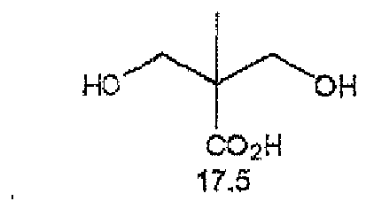
- The components in the following formulation were mixed to obtain the curable composition solution of Example 1. The viscosity at 25°C of this composition was 520 mPa●s (the solid content concentration of the composition was 50 mass%).
Binder solution shown in Table 1 (alkali- soluble binder) 45.0 parts by mass Crosslinking agent shown in Table 1 15.7 parts by mass Acid generator shown in Table 1 2.50 parts by mass Sensitizer shown in Table 1 1.20 parts by mass Silica liquid dispersion shown below (filler, alkali-soluble binder, curing accelerator) 35.7 parts by mass Megaface F-780 (produced by Dainippon Ink and Chemicals, Inc.) (surfactant) 0.13 parts by mass YMF-02 (produced by Sumitomo Metal Mining Co., Ltd., cesium tungsten oxide (a 18.5 mass% liquid dispersion of Cs0.33 WO3 (average dispersed particle diameter: 800 nm or less)) 18.0 parts by mass - The silica liquid dispersion used above was prepared by previously mixing 30 parts by mass of silica (SO-C2, produced by Admatechs Company Limited) (filler), 48.2 parts by mass of Binder Solution A, 0.37 parts by mass of dicyandiamide (curing accelerator) and 59.0 parts by mass of propylene glycol monomethyl ether acetate, and then dispersing the mixture with use of zirconia beads having a diameter of 1.0 mm in a motor mill M-250 (manufactured by Eiger) at a circumferential velocity of 9 m/s for 3 hours.
- The curing composition solutions of Examples 2 to 8 and Reference Example 1 were obtained in the same manner as in Example 1 except for changing the kinds of binder solution (including the binder solution in the silica liquid dispersion), crosslinking agent, acid generator and sensitizer to those shown in Table 1. Here, HS-1 used in Reference Example 1 is not a compound capable of generating an acid upon irradiation with an actinic ray or radiation (acid generator) but is a compound capable of generating a radical upon irradiation with an actinic ray or radiation (radical generator).
Table 1 Example Binder Solution Crosslinking Agent Acid Generator Sensitizer Viscosity (mPa•s) (25°C) Example 1 B-1 K-1 S-1 Z-1 520 Example 2 B-2 K-1 S-2 Z-2 420 Example 3 B-3 K-1 S-2 Z-1 530 Example 4 B-3 K-2 S-3 Z-3 540 Example 5 B-4 K-3 S-4 Z-2 620 Example 6 B-4 K-4 S-1 Z-1 570 Example 7 B-4 K-5 S-1 Z-2 530 Example 8 B-4 K-5 S-3 Z-4 550 Reference Example 1 B-1 HK-1 HS-1 none 500 - B-1: Binder Solution A
- B-2: Binder Solution B
- B-3: A polyamide acid solution obtained by the following synthesis method.
- B-4: A PGMEA solution of 46 mass% polyhydroxystyrene (MARUKA LYNCUR M S-4, produced by Maruzen Petrochemical Co., Ltd.).
- After pouring 12.09 g (0.0375 mol) of 3.3',4,4'-benzophenonetetracarboxylic dianhydride), 2.73 g (0.0125 mol) of pyromellitic dianhydride and 50 g of N-methyl-2-pyrrolidone, these were thoroughly mixed with stirring and cooled to 10°C. Subsequently, 9.41 g (0.047 mol) of 4,4'-diaminodiphenyl ether and 1.1 g (0.003 mol) of (3-amino-4-hydroxyphenyl)hexafluoropropane were dissolved in 30 g of N-methyl-2-pyrrolidone, and the resulting solution was gradually added dropwise to the reaction flask above kept at 10°C. The thus-obtained mixed solution was stirred at 10 to 15°C for 6 hours to obtain Solution B-3 of polyamide acid. Incidentally, the logarithmic viscosity of the N-methyl-2-pyrrolidone solution of polyamide acid was measured at 30°C and found to be 1.4 dl/g.
K-1: 2,4,6-Tris[bis(methoxymethyl)amino]-1,3.5-triazine
K-2: Hexamethylolmelamine
K-3: Xylylenc bisoxetane (OXT-121 produced by Toagosei Co., Ltd.).
K-4: Bisphenol A propylene oxide diglycidyl ether (Epolight 3002, produced by Kyoeisha Chemical Co., Ltd.)K-5: 
- S-1:
- Triphenylsulfonium trifluoromethanesulfonate
- S-2:
- Triphenylsulfonium p-toluenesulfonate
- S-3:
- Bis(4-butoxyphenyl)iodonium p-toluenesulfonate
- S-4:
- Tris(4-chlorophenyl)sulfonium 1-naphthalenesulfonate
- Z-1:
- 9,10-Dibutoxyanthracene
- Z-2:
- N-Ethyl-6-(2-methylbenzoyl)carbazole
- Z-3:
- Michler's ketone
- Z-4:
- Thioxanthone
- HK-1: Bisphenol A diglycidyl ether acryl acid adduct (Epoxy Ester 3000A, produced by Kyoeisha Chemical Co., Ltd.)
- HS-1: 2-(o-methoxystyryl)-4,6-bis(trichloromethyl)-S-triazine (produced by Midori Kagaku Co., Ltd.)
- Each of the curable compositions obtained in Examples 1 to 8 and Reference Example 1 was coated on a silicon wafer by a spin coating method to have a film thickness of 25 µm and then heated on a hot plate at 120°C for 2 minutes to obtain a photosensitive layer.
- The obtained photosensitive layer was irradiated with light in an i-line stepper through a photomask having an island pattern in a square form of 200 µm on a side by changing the exposure dose in steps of 50 mJ/cm2 in the range of 50 to 2,000 mJ/cm2.
- After the irradiation, heating was performed on a hot plate at 120°C for 3 minutes.
- The photosensitive laser after the exposure and heating was subjected to puddle development at 25°C for 40 seconds by using an aqueous 2.38 mass% tetramethylammonium hydroxide solution, then rinsed by spin shower and further washed with pure water to obtain an infrared-blocking solder resist pattern. The minimum exposure dose for obtaining an island pattern of 200 µm on a side when performing the development step for 40 seconds was measured. A smaller numerical value indicates higher sensitivity and is better.
- The curable composition was spin-coated on a glass substrate under the conditions above to form a photosensitive layer (curable composition layer) coating film having a thickness of 25 µm, and the transmittance at a wavelength of 1,200 nm of the coating film was measured using Ultraviolet-Visible-Near Infrared Spectrophotometer UV3600 (manufactured by Shimadzu Corporation). As the numerical value is smaller, the infrared-blocking effect is judged as higher. When the transmittance is 2% or less, the coating film can be said to exhibit a practically good infrared-blocking effect.
- In accordance with (Resist Pattern Formation) above, exposure using the minimum exposure dose and development were performed to form a pattern. The cross-section of the island pattern of 200 µm on a side was observed using an electron microscope (S-4800, manufactured by Hitachi High-Technologies Corporation) and ranked according to the following evaluation criteria.
-
- A: A pattern was formed on the substrate with sufficient adherence and the cross-section of the pattern showed a good rectangular shape. That is, in the cross-sectional profile of the pattern, the difference between the width in the upper layer part of the pattern and the width in the lower layer part (in the vicinity of interface with the substrate) was 7 µm or less.
- B: A pattern was formed on the substrate with sufficient adherence and the cross-section of the pattern showed a good rectangular shape. That is, in the cross-sectional profile of the pattern, the difference between the width in the upper layer part of the pattern and the width in the lower layer part was more than 7 µm and 10 µm or less.
- C: In the cross-sectional profile of the pattern, the difference between the width in the upper layer part of the pattern and the width in the lower layer part was more than 10 µm and 15 µm or less.
- D: In the cross-sectional profile of the pattern, the difference between the width in the upper layer part of the pattern and the width in the lower layer part was more than 15 µm.
- On a silicon wafer as the base material, where wiring was formed in a comb form such that the copper thickness was 12 µm and the copper line/space was 50 µm/50 µm, each of the curable compositions of Examples 1 to 8 and Reference Example 1 was coated by a spin coating method to have a film thickness of 20 µm on the copper. Thereafter, the coating film was heated on a hot plate at 100°C for 2 minutes to obtain a photosensitive layer.
- The obtained photosensitive layer was irradiated with light of a high-pressure mercury lamp at an exposure dose of 800 mJ/cm2.
- The photosensitive laser after the exposure was subjected to puddle development at 25°C for 40 seconds by using an aqueous 2.38 mass% tetramethylammonium hydroxide solution, then rinsed by spin shower, further washed with pure water and thereafter, heat-treated (post-baking) at 150°C for 1 hour to form a solder resist pattern (permanent pattern). With respect to the formed permanent pattern, an electronic component module was left standing in a gas phase at temperatures of -55°C and 125°C each for 30 minutes by using a gas-phase heat/cold shock tester, which was taken as one cycle, and by performing the test under the condition of 300 cycles, the heat/cold shock property of the permanent pattern with respect to the region of 5 cm × 5 cm was evaluated according to the following criteria.
-
- A:
- Cracks were not generated.
- B:
- Cracks were generated but the number of cracks was less than 10.
- C:
- 10 Cracks or more were generated.
- As seen from the results in Table 2, compared with Reference Example 1 where the crosslinking agent is caused to undergo a crosslinking reaction by the action of a radical generated from a radial generator, in Examples where the crosslinking agent is caused to undergo a crosslinking reaction by the action of an acid generated from an acid generator, a pattern satisfying all of the requirements that (1) the light-blocking effect in the infrared region is high, (2) a desired profile and an excellent endurance (heat/cold shock resistance and adherence to substrate) are obtained by alkali development, and (3) the sensitivity in pattern formation is high, can be formed.
- This application is based on a Japanese patent application filed on March 8,2011 (Japanese Patent Application No.
2011-50678 -
- 10
- Silicon substrate
- 12
- Imaging device
- 13
- Interlayer insulating film
- 14
- Base layer
- 15
- Color filter
- 16
- Overcoat
- 17
- Microlens
- 18
- Light-blocking film
- 20
- Adhesive
- 22
- Insulating film
- 23
- Metal electrode
- 24
- Solder resist layer
- 26
- Internal electrode
- 27
- Device surface electrode
- 30
- Glass substrate
- 40
- Imaging lens
- 41
- Adhesive
- 42
- Infrared cut filter
- 43
- Adhesive
- 44
- Light-blocking and electromagnetic shield
- 45
- Adhesive
- 50
- Lens holder
- 60
- Solder ball
- 70
- Circuit substrate
- 100
- Solid-state imaging device substrate
- 200
- Camera module
- 410
- Substrate
- 412, 420
- Lens
- 412a
- Lens surface
- 412b
- Lens edge
- 414
- Light-blocking film
- 414A
- Light-blocking coated layer
- 414a
- Lens opening
- 450
- Dispenser
- 460, 480
- Mold
- 462, 482
- Concave
- 470
- Mask
| Infrared-Blocking Effect (1200 nm) | Minimum Exposure Dose (mJ/cm2) | Evaluation of Pattern | TCT Resistance | |
| Example 1 | <2% | 300 | B | B |
| Example 2 | <2% | 300 | B | B |
| Example 3 | <2% | 150 | A | A |
| Example 4 | <2% | 200 | A | A |
| Example 5 | <2% | 300 | B | B |
| Example 6 | <2% | 300 | B | B |
| Example 7 | <2% | 150 | A | A |
| Example 8 | <2% | 200 | A | A |
| Reference Example 1 | <2% | 300 | C | B |
Claims (17)
- A curable composition for a solid-state imaging device, comprising:(A) an infrared-blocking material,(B) a compound capable of generating an acid upon irradiation with an actinic ray or radiation,(C) a compound caused to undergo a crosslinking reaction by the action of an acid, and(D) a binder resin.
- The curable composition for a solid-state imaging device as claimed in claim 1, wherein the compound (C) is a compound having an oxirane group, a hydroxymethyl group, an alkoxymethyl group or a phenol group.
- The curable composition for a solid-state imaging device as claimed in claim 2, wherein the compound (C) is a compound having two or more oxirane groups, hydroxymethyl groups, alkoxymethyl groups or phenol groups.
- The curable composition for a solid-state imaging device as claimed in any one of claims 1 to 3, wherein the compound (B) is an onium salt compound.
- The curable composition for a solid-state imaging device as claimed in any one of claims 1 to 4, wherein the binder resin (D) has an acid group.
- The curable composition for a solid-state imaging device as claimed in any one of claims 1 to 5, wherein the binder resin (D) is at least either one of a polyamide-based resin and a polyimide-based resin.
- The curable composition for a solid-state imaging device as claimed in any one of claims 1 to 5, wherein the binder resin (D) is a urethane resin.
- The curable composition for a solid-state imaging device as claimed in any one of claims 1 to 7, wherein the infrared-blocking material (A) is a tungsten compound.
- The curable composition for a solid-state imaging device as claimed in any one of claims 1 to 8, wherein the viscosity at 25°C is from 200 to 1,000 mPas.
- A photosensitive layer formed of the curable composition for a solid-state imaging device claimed in any one of claims 1 to 9.
- A permanent pattern formed using the curable composition for a solid-state imaging device claimed in any one of claims 1 to 9.
- The permanent pattern as claimed in claim 11, wherein the permanent pattern is a solder resist layer.
- The permanent pattern as claimed in claim 11, wherein the permanent pattern is an infrared-blocking film.
- A wafer-level lens having a lens and the permanent pattern claimed in claim 11 formed in the circumferential edge part of the lens.
- A solid-state imaging device having the permanent pattern claimed in any one of claims 11 to 13.
- A solid-state imaging device comprising:a solid-state imaging device substrate having an imaging element part formed on one surface thereof, andan infrared-blocking film provided on the other surface side of the solid-state imaging device substrate,wherein the infrared-blocking film is the permanent pattern claimed in claim 13.
- A pattern forming method comprising, in order,
a step of forming the photosensitive layer claimed in claim 10,
a step of patternwise exposing said photosensitive layer to cure the exposed area,
and
a step of removing the unexposed area by alkali development to form a permanent pattern.
Applications Claiming Priority (1)
| Application Number | Priority Date | Filing Date | Title |
|---|---|---|---|
| JP2011050678A JP5417364B2 (en) | 2011-03-08 | 2011-03-08 | Curable composition for solid-state imaging device, photosensitive layer, permanent pattern, wafer level lens, solid-state imaging device, and pattern forming method using the same |
Publications (2)
| Publication Number | Publication Date |
|---|---|
| EP2498130A2 true EP2498130A2 (en) | 2012-09-12 |
| EP2498130A3 EP2498130A3 (en) | 2013-07-03 |
Family
ID=45811372
Family Applications (1)
| Application Number | Title | Priority Date | Filing Date |
|---|---|---|---|
| EP12158562.4A Withdrawn EP2498130A3 (en) | 2011-03-08 | 2012-03-08 | Curable composition for solid-state imaging device, and photosensitive layer, permanent pattern, wafer-level lens, solid-state imaging device and pattern forming method each using the composition |
Country Status (3)
| Country | Link |
|---|---|
| EP (1) | EP2498130A3 (en) |
| JP (1) | JP5417364B2 (en) |
| KR (2) | KR20120102547A (en) |
Cited By (3)
| Publication number | Priority date | Publication date | Assignee | Title |
|---|---|---|---|---|
| CN103923438A (en) * | 2013-01-11 | 2014-07-16 | 株式会社日本触媒 | Resin Composition For Laminating And Use Thereof |
| TWI641649B (en) * | 2013-01-11 | 2018-11-21 | 日本觸媒股份有限公司 | Resin composition for lamination and use thereof |
| CN117430135A (en) * | 2023-12-21 | 2024-01-23 | 山东海化集团有限公司 | Method for synthesizing ferromanganese-based Prussian blue sodium electric positive electrode material and positive electrode material prepared by method |
Families Citing this family (9)
| Publication number | Priority date | Publication date | Assignee | Title |
|---|---|---|---|---|
| KR102142122B1 (en) | 2012-12-12 | 2020-08-06 | 엘지이노텍 주식회사 | Camera Module |
| JP6196109B2 (en) * | 2013-09-20 | 2017-09-13 | 株式会社日本触媒 | Curable resin composition for imaging device and use thereof |
| JP6251529B2 (en) * | 2013-09-20 | 2017-12-20 | 株式会社日本触媒 | Laminate for imaging device and use thereof |
| TWI675907B (en) | 2015-01-21 | 2019-11-01 | 日商Jsr股份有限公司 | Solid imaging device |
| JP2016206503A (en) | 2015-04-24 | 2016-12-08 | Jsr株式会社 | Radiation sensitive resin composition, infrared shielding film, forming method therefor, solid state imaging sensor, and illuminance sensor |
| JP6524786B2 (en) | 2015-04-27 | 2019-06-05 | Jsr株式会社 | Positive radiation sensitive resin composition, infrared shielding film, method for forming the same, solid-state imaging device, illuminance sensor |
| CA3000532A1 (en) * | 2015-10-08 | 2017-04-13 | Basf Se | Preparation of retort packaging ink through cross-linking of polyurethane resins |
| JP7069657B2 (en) * | 2017-11-15 | 2022-05-18 | 昭和電工マテリアルズ株式会社 | Method for manufacturing negative photosensitive resin composition and semiconductor device member |
| WO2024048296A1 (en) * | 2022-08-29 | 2024-03-07 | 富士フイルム株式会社 | Photosensitive composition, transfer film, laminate manufacturing method, laminate, semiconductor package, and resin |
Citations (115)
| Publication number | Priority date | Publication date | Assignee | Title |
|---|---|---|---|---|
| US161811A (en) | 1875-04-06 | Improvement in mechanisms for feeding heel-stiffeners or counter-blanks | ||
| US339049A (en) | 1886-03-30 | Sole-edge-burnishing | ||
| US410201A (en) | 1889-09-03 | Bent for suspension-bridges | ||
| US2833827A (en) | 1955-01-17 | 1958-05-06 | Bayer Ag | Tri (3, 5-di lower alkyl-4-hydroxy phenyl)-sulfonium chlorides and method of preparing same |
| JPS464605Y1 (en) | 1967-01-13 | 1971-02-17 | ||
| JPS4836281A (en) | 1971-09-03 | 1973-05-28 | ||
| US3905815A (en) | 1971-12-17 | 1975-09-16 | Minnesota Mining & Mfg | Photopolymerizable sheet material with diazo resin layer |
| US4069056A (en) | 1974-05-02 | 1978-01-17 | General Electric Company | Photopolymerizable composition containing group Va aromatic onium salts |
| US4069055A (en) | 1974-05-02 | 1978-01-17 | General Electric Company | Photocurable epoxy compositions containing group Va onium salts |
| JPS5437082A (en) | 1977-07-15 | 1979-03-19 | Ici Ltd | Dispersing agent*dispersion liquid containing said agent and paint and ink made from said liquid |
| DE2904626A1 (en) | 1978-02-08 | 1979-08-09 | Minnesota Mining & Mfg | TRIARYLSULFONIUM COMPLEX SALTS, METHOD FOR THE PRODUCTION THEREOF AND PHOTOPOLYMERIZABLE MIXTURES CONTAINING THESE SALTS |
| JPS5425957B2 (en) | 1974-10-04 | 1979-08-31 | ||
| JPS5434327B1 (en) | 1970-12-28 | 1979-10-26 | ||
| JPS5532070A (en) | 1978-08-29 | 1980-03-06 | Fuji Photo Film Co Ltd | Photosensitive resin composition |
| JPS5812577B2 (en) | 1973-12-21 | 1983-03-09 | ヘキスト アクチエンゲゼルシヤフト | Photopolymerizable copying material |
| JPS5944615A (en) | 1982-09-07 | 1984-03-13 | Furuno Electric Co Ltd | Gyro device |
| JPS5953836A (en) | 1982-09-21 | 1984-03-28 | Fuji Photo Film Co Ltd | Photosensitive lithographic plate |
| EP0104143A1 (en) | 1982-09-18 | 1984-03-28 | Ciba-Geigy Ag | Photopolymerizable compositions containing diaryliodosyl salts |
| JPS5971048A (en) | 1982-10-18 | 1984-04-21 | Mitsubishi Chem Ind Ltd | Photopolymerizable photosensitive composition |
| US4508811A (en) | 1983-01-17 | 1985-04-02 | U.S. Philips Corporation | Recording element having a pyrylium or thiopyrylium-squarylium dye layer and new pyrylium or thiopyrylium-squarylium compounds |
| JPS60239736A (en) | 1984-05-14 | 1985-11-28 | Fuji Photo Film Co Ltd | Photosensitive composition |
| JPS61166544A (en) | 1985-01-18 | 1986-07-28 | Fuji Photo Film Co Ltd | Photosolubilizable composition |
| JPS61169837A (en) | 1985-01-22 | 1986-07-31 | Fuji Photo Film Co Ltd | Photosolubilizable composition |
| JPS61169835A (en) | 1985-01-22 | 1986-07-31 | Fuji Photo Film Co Ltd | Photosolubilizable composition |
| JPS6258241A (en) | 1985-09-09 | 1987-03-13 | Fuji Photo Film Co Ltd | Photosensitive composition |
| JPS62143044A (en) | 1985-11-20 | 1987-06-26 | サイカラー・インコーポレーテッド | Photosetting composition containing dye borate complex and photosensitive material using the same |
| JPS62150242A (en) | 1985-11-20 | 1987-07-04 | サイカラー・インコーポレーテッド | Photosensitive material containing ion dye compound as initiator |
| DE3604580A1 (en) | 1986-02-14 | 1987-08-20 | Basf Ag | CURABLE MIXTURES CONTAINING N-SULFONYLAMINOSULFONIUM SALTS AS CATIONICALLY EFFECTIVE CATALYSTS |
| DE3604581A1 (en) | 1986-02-14 | 1987-08-20 | Basf Ag | 4-Acylbenzylsulphonium salts, their preparation, and photocurable mixtures and recording materials containing these compounds |
| JPS62212401A (en) | 1986-03-14 | 1987-09-18 | Fuji Photo Film Co Ltd | Photopolymerizable composition |
| JPS6370243A (en) | 1986-09-11 | 1988-03-30 | Fuji Photo Film Co Ltd | Photosensitive composition |
| US4760013A (en) | 1987-02-17 | 1988-07-26 | International Business Machines Corporation | Sulfonium salt photoinitiators |
| JPS63298339A (en) | 1987-05-29 | 1988-12-06 | Fuji Photo Film Co Ltd | Photosensitive composition |
| EP0297443A2 (en) | 1987-07-01 | 1989-01-04 | BASF Aktiengesellschaft | Light sensitive mixture for light sensitive coating materials |
| EP0297442A1 (en) | 1987-07-01 | 1989-01-04 | BASF Aktiengesellschaft | Sulfonium salts comprising groups which are labile in acid environment |
| EP0370693A2 (en) | 1988-11-21 | 1990-05-30 | Eastman Kodak Company | Novel onium salts and the use thereof as photoinitiators |
| JPH02150848A (en) | 1988-12-02 | 1990-06-11 | Hitachi Ltd | Photofadable and radiation sensitive composition and pattern forming method by using this composition |
| US4933377A (en) | 1988-02-29 | 1990-06-12 | Saeva Franklin D | Novel sulfonium salts and the use thereof as photoinitiators |
| EP0390214A2 (en) | 1989-03-31 | 1990-10-03 | E.F. Johnson Company | Method and apparatus for a distributive wide area network for a land mobile transmission trunked communication system |
| JPH02272009A (en) | 1989-04-13 | 1990-11-06 | Mitsubishi Kasei Corp | Polyester macromonomer |
| JPH02296514A (en) | 1989-05-12 | 1990-12-07 | Matsushita Electric Ind Co Ltd | Suspension controller for vehicle |
| JPH03112992A (en) | 1989-09-14 | 1991-05-14 | Byk Chem Gmbh | Phosphoric acid esters, their preparation and their use as dispersant |
| JPH03172301A (en) | 1989-11-30 | 1991-07-25 | Tamura Kaken Kk | Photosensitive resin composition |
| JPH04365049A (en) | 1991-06-12 | 1992-12-17 | Fuji Photo Film Co Ltd | Photosensitive composition material |
| JPH059407A (en) | 1990-12-18 | 1993-01-19 | Ciba Geigy Ag | Photosensitive composition containing water as solvent or dispersing agent |
| US5227227A (en) | 1990-03-05 | 1993-07-13 | Johnson & Johnson Inc. | Non-woven fabric with a thermally activated adhesive surface, resulting product and applications thereof |
| EP0568993A2 (en) | 1992-05-06 | 1993-11-10 | Kyowa Hakko Kogyo Co., Ltd. | Chemical amplification resist composition |
| JPH06157623A (en) | 1992-08-14 | 1994-06-07 | Toyo Ink Mfg Co Ltd | Polymerizable composition and method for polymerization |
| JPH06175564A (en) | 1992-12-04 | 1994-06-24 | Toyo Ink Mfg Co Ltd | Hologram recording material and production of volume phase type hologram by using the recording material |
| JPH06175561A (en) | 1992-12-04 | 1994-06-24 | Toyo Ink Mfg Co Ltd | Hologram recording medium and production of volume phase type hologram by using the recording medium |
| JPH06175553A (en) | 1992-12-03 | 1994-06-24 | Toyo Ink Mfg Co Ltd | Hologram recording medium and production of volume phase type hologram by using this medium |
| JPH06175554A (en) | 1992-12-03 | 1994-06-24 | Toyo Ink Mfg Co Ltd | Production of volume phase type hologram |
| JPH06295060A (en) | 1992-10-29 | 1994-10-21 | Ajinomoto Co Inc | Photosensitive resin composition or photosensitive thermosetting resin composition, and photosolder resist composition using these |
| JPH06348011A (en) | 1993-06-04 | 1994-12-22 | Toyo Ink Mfg Co Ltd | Photopolymerizable composition |
| JPH07128867A (en) | 1993-06-28 | 1995-05-19 | Tokyo Ohka Kogyo Co Ltd | Solvent for washing and removing resist and production of substrate for producing electronic parts with same |
| JPH07128785A (en) | 1993-11-02 | 1995-05-19 | Konica Corp | Material and method for forming image |
| JPH07140589A (en) | 1993-11-19 | 1995-06-02 | Konica Corp | Image forming material and image forming method |
| JPH07146562A (en) | 1993-06-28 | 1995-06-06 | Tokyo Ohka Kogyo Co Ltd | Solvent for washing and removing resist and production of base material for producing electronic parts with the same |
| JPH0768256B2 (en) | 1991-08-01 | 1995-07-26 | 株式会社ジャパンエナジー | Novel imidazole silane compound, method for producing the same, and metal surface treating agent using the same |
| JPH07292014A (en) | 1994-04-25 | 1995-11-07 | Nippon Paint Co Ltd | Near-infrared-polymerizable composition |
| JPH07306527A (en) | 1994-05-11 | 1995-11-21 | Konica Corp | Image forming material and image forming method |
| JPH07319161A (en) | 1994-05-27 | 1995-12-08 | Hitachi Chem Co Ltd | Photosensitive liquid containing color image forming material, photosensitive element using that and production of color filter |
| JPH08507960A (en) | 1993-03-25 | 1996-08-27 | ゼネカ・リミテッド | Dispersant |
| JPH08278637A (en) | 1995-04-05 | 1996-10-22 | Mitsubishi Chem Corp | Washing solution and washing method |
| JPH0977994A (en) | 1995-09-18 | 1997-03-25 | Toyo Ink Mfg Co Ltd | Pigment dispersant for nonaqueous system, pigment composition containing the same, and nonaqueous pigment dispersion |
| JPH09169821A (en) | 1995-10-16 | 1997-06-30 | Ajinomoto Co Inc | Pigment dispersant |
| JPH09188710A (en) | 1995-11-24 | 1997-07-22 | Ciba Geigy Ag | Borate photoinitiator derived from monoborane |
| JPH09188685A (en) | 1995-11-24 | 1997-07-22 | Ciba Geigy Ag | Borate auxiliary initiator for photo polymerization |
| JPH09188686A (en) | 1995-11-24 | 1997-07-22 | Ciba Geigy Ag | Borate salt for photo polymerization initiator stable in acidic medium |
| JP2763775B2 (en) | 1988-05-17 | 1998-06-11 | ダイセル化学工業株式会社 | Active energy ray-curable unsaturated resin composition |
| JP2764769B2 (en) | 1991-06-24 | 1998-06-11 | 富士写真フイルム株式会社 | Photopolymerizable composition |
| JPH10300922A (en) | 1997-04-30 | 1998-11-13 | Jsr Corp | Radiation sensitive composition for color filter |
| JPH10339949A (en) | 1997-04-10 | 1998-12-22 | Fuji Photo Film Co Ltd | Pigment dispersed composition, colored photosensitive composition using same and novel compound |
| JPH11240930A (en) | 1997-11-28 | 1999-09-07 | Hitachi Chem Co Ltd | Photocurable resin composition and photosensitive element using the same |
| JPH11271969A (en) | 1998-01-21 | 1999-10-08 | Mitsubishi Chemical Corp | Photopolymerizable composition and photosensitive lithographic printing plate |
| JP2000066385A (en) | 1998-08-18 | 2000-03-03 | Ciba Specialty Chem Holding Inc | SULFONYL OXIMES FOR HIGH SENSITIVITY THICK i-LINE PHOTORESIST |
| EP0993966A1 (en) | 1998-10-13 | 2000-04-19 | Agfa-Gevaert AG | Negativ-working radiation-sensitive mixture for the production of a recording material which is imageable by heat or infrared laser beams |
| JP2000131837A (en) | 1998-08-17 | 2000-05-12 | Mitsubishi Chemicals Corp | Photopolymerizable composition, photopolymerizable planographic printing plate and image forming method |
| JP2000232264A (en) | 1998-12-09 | 2000-08-22 | Goo Chemical Co Ltd | Photo solder resist ink |
| JP2000273370A (en) | 1999-03-25 | 2000-10-03 | Fuji Photo Film Co Ltd | Cleaning liquid for colored composition |
| JP2000310808A (en) | 1999-04-26 | 2000-11-07 | Canon Inc | Illumination device and photographic device using the same |
| JP2001125255A (en) | 1999-10-27 | 2001-05-11 | Fuji Photo Film Co Ltd | Photosensitive lithographic printing plate |
| JP2001132318A (en) | 1999-10-29 | 2001-05-15 | Oi Seisakusho Co Ltd | Opening/closing device of opening/closing body for vehicle |
| JP2001318463A (en) | 2000-05-11 | 2001-11-16 | Fuji Photo Film Co Ltd | Negative type original plate of planographic printing plate |
| JP2002107916A (en) | 2000-09-27 | 2002-04-10 | Fuji Photo Film Co Ltd | Original plate for planographic printing plate |
| EP1204000A1 (en) | 2000-11-06 | 2002-05-08 | Fuji Photo Film Co., Ltd. | Photosensitive lithographic printing plate |
| JP2002273191A (en) | 2001-03-21 | 2002-09-24 | Dainippon Printing Co Ltd | Pigment dispersant and photosensitive coloring composition |
| JP2003049110A (en) | 2001-05-21 | 2003-02-21 | Ciba Specialty Chem Holding Inc | Pigment composition comprising dispersant of modified block copolymer |
| JP2003238837A (en) | 2002-02-14 | 2003-08-27 | Fuji Photo Film Co Ltd | Pigment dispersant, pigment dispersion composition and colored photosensitive composition comprising the dispersant |
| JP2003262958A (en) | 2002-03-11 | 2003-09-19 | Fuji Photo Film Co Ltd | Image recording material |
| JP2003533455A (en) | 2000-05-18 | 2003-11-11 | カー コーポレイション | Polymerizable dispersant |
| JP2004037986A (en) | 2002-07-05 | 2004-02-05 | Jsr Corp | Radiation sensitive composition for color filter, color filter and color liquid crystal display element |
| JP2004300204A (en) | 2003-03-28 | 2004-10-28 | Nippon Shokubai Co Ltd | Curable resin composition and its use |
| JP2006063550A (en) | 2004-08-25 | 2006-03-09 | Okawa Kogyo Kk | Portable awning frame |
| JP2006085140A (en) | 2004-08-20 | 2006-03-30 | Tokyo Ohka Kogyo Co Ltd | Solvent for cleaning and removing |
| JP2006291191A (en) | 2005-03-18 | 2006-10-26 | Dainippon Printing Co Ltd | Cleaning liquid for photosensitive colored composition and method for evaluating the same |
| JP2007002102A (en) | 2005-06-23 | 2007-01-11 | Tokyo Ohka Kogyo Co Ltd | Cleanser, and method for removing resin composition therewith |
| JP2007002101A (en) | 2005-06-23 | 2007-01-11 | Tokyo Ohka Kogyo Co Ltd | Cleanser |
| JP2007277514A (en) | 2006-03-17 | 2007-10-25 | Fujifilm Corp | Polymer compound and method for producing the same, pigment dispersant, pigment dispersing composition, photocurable composition and color filter and method for producing the same |
| JP2007291523A (en) | 2006-04-20 | 2007-11-08 | Joma Internatl As | Coating formed by thermal spraying, and its forming method |
| JP2008009426A (en) | 2006-06-02 | 2008-01-17 | Fujifilm Corp | Pigment dispersion composition, photo-curing composition, color filter using the same, and manufacturing method of the color filter |
| JP2008029901A (en) | 2005-07-08 | 2008-02-14 | Toyo Ink Mfg Co Ltd | Dispersant, its manufacturing method and pigment dispersion containing the dispersant |
| JP2008081732A (en) | 2006-09-01 | 2008-04-10 | Fujifilm Corp | Pigment dispersion composition, photocurable composition, color filter, and manufacturing method of color filter |
| JP4096205B2 (en) | 2003-10-20 | 2008-06-04 | 住友金属鉱山株式会社 | Infrared shielding material fine particle dispersion, infrared shielding body, method for producing infrared shielding material fine particles, and infrared shielding material fine particles |
| JP2008250074A (en) | 2007-03-30 | 2008-10-16 | Fujifilm Corp | Photosensitive resin composition, photosensitive film, photosensitive laminate, method for forming permanent pattern and printed board |
| JP2008257045A (en) | 2007-04-06 | 2008-10-23 | Taiyo Ink Mfg Ltd | Black solder resist composition and cured product thereof |
| JP2009052010A (en) | 2007-07-27 | 2009-03-12 | Mitsubishi Chemicals Corp | Pigment dispersion, coloring composition for color filter, color filter, and liquid crystal display |
| JP2009099591A (en) | 2007-10-12 | 2009-05-07 | Toshiba Corp | Solid-state image sensor and method of manufacturing the same |
| JP2009158863A (en) | 2007-12-27 | 2009-07-16 | Toshiba Corp | Semiconductor package and camera module |
| JP2009194396A (en) | 2003-08-28 | 2009-08-27 | Fujikura Ltd | Semiconductor package and method of manufacturing the same |
| JP2009205029A (en) | 2008-02-29 | 2009-09-10 | Dainippon Printing Co Ltd | Near-infrared light absorbing material |
| JP2009203462A (en) | 2008-01-31 | 2009-09-10 | Fujifilm Corp | Resin, pigment dispersion, colored curable composition, color filter using it and its production method |
| JP2009258668A (en) | 2008-03-17 | 2009-11-05 | Fujifilm Corp | Coloring curable composition, color filter and method for producing color filter |
| JP2010106268A (en) | 2008-10-03 | 2010-05-13 | Fujifilm Corp | Dispersed composition, polymerizable composition, light-shielding color filter, solid-state imaging element, liquid crystal display device, wafer-level lens, and imaging unit |
| JP2011050678A (en) | 2009-09-04 | 2011-03-17 | Kao Corp | Container for cosmetics |
Family Cites Families (8)
| Publication number | Priority date | Publication date | Assignee | Title |
|---|---|---|---|---|
| JP2006284947A (en) * | 2005-03-31 | 2006-10-19 | Fuji Photo Film Co Ltd | Photosensitive resin composition for light shielding film, method for fabricating light shielding film, transfer material, and method for manufacturing transfer material |
| JP4809006B2 (en) * | 2005-07-05 | 2011-11-02 | 太陽ホールディングス株式会社 | Colored photosensitive resin composition and cured product thereof |
| CN101688935A (en) * | 2007-08-22 | 2010-03-31 | 三菱化学株式会社 | Resin black matrix, light blocking photosensitive resin composition, tft element substrate and liquid crystal display device |
| JP5343494B2 (en) * | 2008-09-30 | 2013-11-13 | デクセリアルズ株式会社 | Photosensitive siloxane polyimide resin composition |
| JP2010237303A (en) * | 2009-03-30 | 2010-10-21 | Fujifilm Corp | Negative planographic printing plate original plate |
| JP2010276825A (en) * | 2009-05-28 | 2010-12-09 | Fujifilm Corp | Negative lithographic printing plate precursor, method for producing the same and plate making method for lithographic printing plate |
| KR101913997B1 (en) * | 2009-12-04 | 2018-10-31 | 도레이 카부시키가이샤 | Photosensitive resin composition, laminate utilizing same, and solid-state imaging device |
| JP2011215597A (en) * | 2010-03-15 | 2011-10-27 | Jsr Corp | Radiation-sensitive composition, method for forming insulating film, insulating film and solid-state imaging element |
-
2011
- 2011-03-08 JP JP2011050678A patent/JP5417364B2/en active Active
-
2012
- 2012-03-08 KR KR1020120023760A patent/KR20120102547A/en active Application Filing
- 2012-03-08 EP EP12158562.4A patent/EP2498130A3/en not_active Withdrawn
-
2015
- 2015-01-22 KR KR1020150010672A patent/KR20150013932A/en not_active Application Discontinuation
Patent Citations (117)
| Publication number | Priority date | Publication date | Assignee | Title |
|---|---|---|---|---|
| US339049A (en) | 1886-03-30 | Sole-edge-burnishing | ||
| US410201A (en) | 1889-09-03 | Bent for suspension-bridges | ||
| US161811A (en) | 1875-04-06 | Improvement in mechanisms for feeding heel-stiffeners or counter-blanks | ||
| US2833827A (en) | 1955-01-17 | 1958-05-06 | Bayer Ag | Tri (3, 5-di lower alkyl-4-hydroxy phenyl)-sulfonium chlorides and method of preparing same |
| JPS464605Y1 (en) | 1967-01-13 | 1971-02-17 | ||
| JPS5434327B1 (en) | 1970-12-28 | 1979-10-26 | ||
| JPS4836281A (en) | 1971-09-03 | 1973-05-28 | ||
| US3905815A (en) | 1971-12-17 | 1975-09-16 | Minnesota Mining & Mfg | Photopolymerizable sheet material with diazo resin layer |
| JPS5812577B2 (en) | 1973-12-21 | 1983-03-09 | ヘキスト アクチエンゲゼルシヤフト | Photopolymerizable copying material |
| US4069056A (en) | 1974-05-02 | 1978-01-17 | General Electric Company | Photopolymerizable composition containing group Va aromatic onium salts |
| US4069055A (en) | 1974-05-02 | 1978-01-17 | General Electric Company | Photocurable epoxy compositions containing group Va onium salts |
| JPS5425957B2 (en) | 1974-10-04 | 1979-08-31 | ||
| JPS5437082A (en) | 1977-07-15 | 1979-03-19 | Ici Ltd | Dispersing agent*dispersion liquid containing said agent and paint and ink made from said liquid |
| DE2904626A1 (en) | 1978-02-08 | 1979-08-09 | Minnesota Mining & Mfg | TRIARYLSULFONIUM COMPLEX SALTS, METHOD FOR THE PRODUCTION THEREOF AND PHOTOPOLYMERIZABLE MIXTURES CONTAINING THESE SALTS |
| JPS5532070A (en) | 1978-08-29 | 1980-03-06 | Fuji Photo Film Co Ltd | Photosensitive resin composition |
| JPS5944615A (en) | 1982-09-07 | 1984-03-13 | Furuno Electric Co Ltd | Gyro device |
| EP0104143A1 (en) | 1982-09-18 | 1984-03-28 | Ciba-Geigy Ag | Photopolymerizable compositions containing diaryliodosyl salts |
| JPS5953836A (en) | 1982-09-21 | 1984-03-28 | Fuji Photo Film Co Ltd | Photosensitive lithographic plate |
| JPS5971048A (en) | 1982-10-18 | 1984-04-21 | Mitsubishi Chem Ind Ltd | Photopolymerizable photosensitive composition |
| US4508811A (en) | 1983-01-17 | 1985-04-02 | U.S. Philips Corporation | Recording element having a pyrylium or thiopyrylium-squarylium dye layer and new pyrylium or thiopyrylium-squarylium compounds |
| JPS60239736A (en) | 1984-05-14 | 1985-11-28 | Fuji Photo Film Co Ltd | Photosensitive composition |
| JPS61166544A (en) | 1985-01-18 | 1986-07-28 | Fuji Photo Film Co Ltd | Photosolubilizable composition |
| JPS61169837A (en) | 1985-01-22 | 1986-07-31 | Fuji Photo Film Co Ltd | Photosolubilizable composition |
| JPS61169835A (en) | 1985-01-22 | 1986-07-31 | Fuji Photo Film Co Ltd | Photosolubilizable composition |
| JPS6258241A (en) | 1985-09-09 | 1987-03-13 | Fuji Photo Film Co Ltd | Photosensitive composition |
| JPS62143044A (en) | 1985-11-20 | 1987-06-26 | サイカラー・インコーポレーテッド | Photosetting composition containing dye borate complex and photosensitive material using the same |
| JPS62150242A (en) | 1985-11-20 | 1987-07-04 | サイカラー・インコーポレーテッド | Photosensitive material containing ion dye compound as initiator |
| US4734444A (en) | 1986-02-14 | 1988-03-29 | Basf Aktiengesellschaft | Curable mixtures containing N-sulfonylaminosulfonium salts as cationically active catalysts |
| DE3604580A1 (en) | 1986-02-14 | 1987-08-20 | Basf Ag | CURABLE MIXTURES CONTAINING N-SULFONYLAMINOSULFONIUM SALTS AS CATIONICALLY EFFECTIVE CATALYSTS |
| EP0233567A2 (en) | 1986-02-14 | 1987-08-26 | BASF Aktiengesellschaft | Curable compositions containing N-sulfonylaminosulfonium salts as cationically active catalysts |
| DE3604581A1 (en) | 1986-02-14 | 1987-08-20 | Basf Ag | 4-Acylbenzylsulphonium salts, their preparation, and photocurable mixtures and recording materials containing these compounds |
| JPS62212401A (en) | 1986-03-14 | 1987-09-18 | Fuji Photo Film Co Ltd | Photopolymerizable composition |
| JPS6370243A (en) | 1986-09-11 | 1988-03-30 | Fuji Photo Film Co Ltd | Photosensitive composition |
| US4760013A (en) | 1987-02-17 | 1988-07-26 | International Business Machines Corporation | Sulfonium salt photoinitiators |
| JPS63298339A (en) | 1987-05-29 | 1988-12-06 | Fuji Photo Film Co Ltd | Photosensitive composition |
| EP0297442A1 (en) | 1987-07-01 | 1989-01-04 | BASF Aktiengesellschaft | Sulfonium salts comprising groups which are labile in acid environment |
| EP0297443A2 (en) | 1987-07-01 | 1989-01-04 | BASF Aktiengesellschaft | Light sensitive mixture for light sensitive coating materials |
| US4933377A (en) | 1988-02-29 | 1990-06-12 | Saeva Franklin D | Novel sulfonium salts and the use thereof as photoinitiators |
| JP2763775B2 (en) | 1988-05-17 | 1998-06-11 | ダイセル化学工業株式会社 | Active energy ray-curable unsaturated resin composition |
| EP0370693A2 (en) | 1988-11-21 | 1990-05-30 | Eastman Kodak Company | Novel onium salts and the use thereof as photoinitiators |
| JPH02150848A (en) | 1988-12-02 | 1990-06-11 | Hitachi Ltd | Photofadable and radiation sensitive composition and pattern forming method by using this composition |
| EP0390214A2 (en) | 1989-03-31 | 1990-10-03 | E.F. Johnson Company | Method and apparatus for a distributive wide area network for a land mobile transmission trunked communication system |
| JPH02272009A (en) | 1989-04-13 | 1990-11-06 | Mitsubishi Kasei Corp | Polyester macromonomer |
| JPH02296514A (en) | 1989-05-12 | 1990-12-07 | Matsushita Electric Ind Co Ltd | Suspension controller for vehicle |
| JPH03112992A (en) | 1989-09-14 | 1991-05-14 | Byk Chem Gmbh | Phosphoric acid esters, their preparation and their use as dispersant |
| JPH03172301A (en) | 1989-11-30 | 1991-07-25 | Tamura Kaken Kk | Photosensitive resin composition |
| US5227227A (en) | 1990-03-05 | 1993-07-13 | Johnson & Johnson Inc. | Non-woven fabric with a thermally activated adhesive surface, resulting product and applications thereof |
| JPH059407A (en) | 1990-12-18 | 1993-01-19 | Ciba Geigy Ag | Photosensitive composition containing water as solvent or dispersing agent |
| JPH04365049A (en) | 1991-06-12 | 1992-12-17 | Fuji Photo Film Co Ltd | Photosensitive composition material |
| JP2764769B2 (en) | 1991-06-24 | 1998-06-11 | 富士写真フイルム株式会社 | Photopolymerizable composition |
| JPH0768256B2 (en) | 1991-08-01 | 1995-07-26 | 株式会社ジャパンエナジー | Novel imidazole silane compound, method for producing the same, and metal surface treating agent using the same |
| EP0568993A2 (en) | 1992-05-06 | 1993-11-10 | Kyowa Hakko Kogyo Co., Ltd. | Chemical amplification resist composition |
| JPH06157623A (en) | 1992-08-14 | 1994-06-07 | Toyo Ink Mfg Co Ltd | Polymerizable composition and method for polymerization |
| JPH06295060A (en) | 1992-10-29 | 1994-10-21 | Ajinomoto Co Inc | Photosensitive resin composition or photosensitive thermosetting resin composition, and photosolder resist composition using these |
| JPH06175554A (en) | 1992-12-03 | 1994-06-24 | Toyo Ink Mfg Co Ltd | Production of volume phase type hologram |
| JPH06175553A (en) | 1992-12-03 | 1994-06-24 | Toyo Ink Mfg Co Ltd | Hologram recording medium and production of volume phase type hologram by using this medium |
| JPH06175561A (en) | 1992-12-04 | 1994-06-24 | Toyo Ink Mfg Co Ltd | Hologram recording medium and production of volume phase type hologram by using the recording medium |
| JPH06175564A (en) | 1992-12-04 | 1994-06-24 | Toyo Ink Mfg Co Ltd | Hologram recording material and production of volume phase type hologram by using the recording material |
| JPH08507960A (en) | 1993-03-25 | 1996-08-27 | ゼネカ・リミテッド | Dispersant |
| JPH06348011A (en) | 1993-06-04 | 1994-12-22 | Toyo Ink Mfg Co Ltd | Photopolymerizable composition |
| JPH07128867A (en) | 1993-06-28 | 1995-05-19 | Tokyo Ohka Kogyo Co Ltd | Solvent for washing and removing resist and production of substrate for producing electronic parts with same |
| JPH07146562A (en) | 1993-06-28 | 1995-06-06 | Tokyo Ohka Kogyo Co Ltd | Solvent for washing and removing resist and production of base material for producing electronic parts with the same |
| JPH07128785A (en) | 1993-11-02 | 1995-05-19 | Konica Corp | Material and method for forming image |
| JPH07140589A (en) | 1993-11-19 | 1995-06-02 | Konica Corp | Image forming material and image forming method |
| JPH07292014A (en) | 1994-04-25 | 1995-11-07 | Nippon Paint Co Ltd | Near-infrared-polymerizable composition |
| JPH07306527A (en) | 1994-05-11 | 1995-11-21 | Konica Corp | Image forming material and image forming method |
| JPH07319161A (en) | 1994-05-27 | 1995-12-08 | Hitachi Chem Co Ltd | Photosensitive liquid containing color image forming material, photosensitive element using that and production of color filter |
| JPH08278637A (en) | 1995-04-05 | 1996-10-22 | Mitsubishi Chem Corp | Washing solution and washing method |
| JPH0977994A (en) | 1995-09-18 | 1997-03-25 | Toyo Ink Mfg Co Ltd | Pigment dispersant for nonaqueous system, pigment composition containing the same, and nonaqueous pigment dispersion |
| JPH09169821A (en) | 1995-10-16 | 1997-06-30 | Ajinomoto Co Inc | Pigment dispersant |
| JPH09188710A (en) | 1995-11-24 | 1997-07-22 | Ciba Geigy Ag | Borate photoinitiator derived from monoborane |
| JPH09188685A (en) | 1995-11-24 | 1997-07-22 | Ciba Geigy Ag | Borate auxiliary initiator for photo polymerization |
| JPH09188686A (en) | 1995-11-24 | 1997-07-22 | Ciba Geigy Ag | Borate salt for photo polymerization initiator stable in acidic medium |
| JPH10339949A (en) | 1997-04-10 | 1998-12-22 | Fuji Photo Film Co Ltd | Pigment dispersed composition, colored photosensitive composition using same and novel compound |
| JPH10300922A (en) | 1997-04-30 | 1998-11-13 | Jsr Corp | Radiation sensitive composition for color filter |
| JPH11240930A (en) | 1997-11-28 | 1999-09-07 | Hitachi Chem Co Ltd | Photocurable resin composition and photosensitive element using the same |
| JPH11271969A (en) | 1998-01-21 | 1999-10-08 | Mitsubishi Chemical Corp | Photopolymerizable composition and photosensitive lithographic printing plate |
| JP2000131837A (en) | 1998-08-17 | 2000-05-12 | Mitsubishi Chemicals Corp | Photopolymerizable composition, photopolymerizable planographic printing plate and image forming method |
| JP2000066385A (en) | 1998-08-18 | 2000-03-03 | Ciba Specialty Chem Holding Inc | SULFONYL OXIMES FOR HIGH SENSITIVITY THICK i-LINE PHOTORESIST |
| EP0993966A1 (en) | 1998-10-13 | 2000-04-19 | Agfa-Gevaert AG | Negativ-working radiation-sensitive mixture for the production of a recording material which is imageable by heat or infrared laser beams |
| JP2000232264A (en) | 1998-12-09 | 2000-08-22 | Goo Chemical Co Ltd | Photo solder resist ink |
| JP2000273370A (en) | 1999-03-25 | 2000-10-03 | Fuji Photo Film Co Ltd | Cleaning liquid for colored composition |
| JP2000310808A (en) | 1999-04-26 | 2000-11-07 | Canon Inc | Illumination device and photographic device using the same |
| JP2001125255A (en) | 1999-10-27 | 2001-05-11 | Fuji Photo Film Co Ltd | Photosensitive lithographic printing plate |
| JP2001132318A (en) | 1999-10-29 | 2001-05-15 | Oi Seisakusho Co Ltd | Opening/closing device of opening/closing body for vehicle |
| JP2001318463A (en) | 2000-05-11 | 2001-11-16 | Fuji Photo Film Co Ltd | Negative type original plate of planographic printing plate |
| JP2003533455A (en) | 2000-05-18 | 2003-11-11 | カー コーポレイション | Polymerizable dispersant |
| JP2002107916A (en) | 2000-09-27 | 2002-04-10 | Fuji Photo Film Co Ltd | Original plate for planographic printing plate |
| EP1204000A1 (en) | 2000-11-06 | 2002-05-08 | Fuji Photo Film Co., Ltd. | Photosensitive lithographic printing plate |
| JP2002273191A (en) | 2001-03-21 | 2002-09-24 | Dainippon Printing Co Ltd | Pigment dispersant and photosensitive coloring composition |
| JP2003049110A (en) | 2001-05-21 | 2003-02-21 | Ciba Specialty Chem Holding Inc | Pigment composition comprising dispersant of modified block copolymer |
| JP2003238837A (en) | 2002-02-14 | 2003-08-27 | Fuji Photo Film Co Ltd | Pigment dispersant, pigment dispersion composition and colored photosensitive composition comprising the dispersant |
| JP2003262958A (en) | 2002-03-11 | 2003-09-19 | Fuji Photo Film Co Ltd | Image recording material |
| JP2004037986A (en) | 2002-07-05 | 2004-02-05 | Jsr Corp | Radiation sensitive composition for color filter, color filter and color liquid crystal display element |
| JP2004300204A (en) | 2003-03-28 | 2004-10-28 | Nippon Shokubai Co Ltd | Curable resin composition and its use |
| JP2009194396A (en) | 2003-08-28 | 2009-08-27 | Fujikura Ltd | Semiconductor package and method of manufacturing the same |
| JP4096205B2 (en) | 2003-10-20 | 2008-06-04 | 住友金属鉱山株式会社 | Infrared shielding material fine particle dispersion, infrared shielding body, method for producing infrared shielding material fine particles, and infrared shielding material fine particles |
| JP2006085140A (en) | 2004-08-20 | 2006-03-30 | Tokyo Ohka Kogyo Co Ltd | Solvent for cleaning and removing |
| JP2006063550A (en) | 2004-08-25 | 2006-03-09 | Okawa Kogyo Kk | Portable awning frame |
| JP2006291191A (en) | 2005-03-18 | 2006-10-26 | Dainippon Printing Co Ltd | Cleaning liquid for photosensitive colored composition and method for evaluating the same |
| JP2007002102A (en) | 2005-06-23 | 2007-01-11 | Tokyo Ohka Kogyo Co Ltd | Cleanser, and method for removing resin composition therewith |
| JP2007002101A (en) | 2005-06-23 | 2007-01-11 | Tokyo Ohka Kogyo Co Ltd | Cleanser |
| JP2008029901A (en) | 2005-07-08 | 2008-02-14 | Toyo Ink Mfg Co Ltd | Dispersant, its manufacturing method and pigment dispersion containing the dispersant |
| JP2007277514A (en) | 2006-03-17 | 2007-10-25 | Fujifilm Corp | Polymer compound and method for producing the same, pigment dispersant, pigment dispersing composition, photocurable composition and color filter and method for producing the same |
| JP2007291523A (en) | 2006-04-20 | 2007-11-08 | Joma Internatl As | Coating formed by thermal spraying, and its forming method |
| JP2008009426A (en) | 2006-06-02 | 2008-01-17 | Fujifilm Corp | Pigment dispersion composition, photo-curing composition, color filter using the same, and manufacturing method of the color filter |
| JP2008081732A (en) | 2006-09-01 | 2008-04-10 | Fujifilm Corp | Pigment dispersion composition, photocurable composition, color filter, and manufacturing method of color filter |
| JP2008250074A (en) | 2007-03-30 | 2008-10-16 | Fujifilm Corp | Photosensitive resin composition, photosensitive film, photosensitive laminate, method for forming permanent pattern and printed board |
| JP2008257045A (en) | 2007-04-06 | 2008-10-23 | Taiyo Ink Mfg Ltd | Black solder resist composition and cured product thereof |
| JP2009052010A (en) | 2007-07-27 | 2009-03-12 | Mitsubishi Chemicals Corp | Pigment dispersion, coloring composition for color filter, color filter, and liquid crystal display |
| JP2009099591A (en) | 2007-10-12 | 2009-05-07 | Toshiba Corp | Solid-state image sensor and method of manufacturing the same |
| JP2009158863A (en) | 2007-12-27 | 2009-07-16 | Toshiba Corp | Semiconductor package and camera module |
| JP2009203462A (en) | 2008-01-31 | 2009-09-10 | Fujifilm Corp | Resin, pigment dispersion, colored curable composition, color filter using it and its production method |
| JP2009205029A (en) | 2008-02-29 | 2009-09-10 | Dainippon Printing Co Ltd | Near-infrared light absorbing material |
| JP2009258668A (en) | 2008-03-17 | 2009-11-05 | Fujifilm Corp | Coloring curable composition, color filter and method for producing color filter |
| JP2010106268A (en) | 2008-10-03 | 2010-05-13 | Fujifilm Corp | Dispersed composition, polymerizable composition, light-shielding color filter, solid-state imaging element, liquid crystal display device, wafer-level lens, and imaging unit |
| JP2011050678A (en) | 2009-09-04 | 2011-03-17 | Kao Corp | Container for cosmetics |
Non-Patent Citations (9)
| Title |
|---|
| C.S. WEN ET AL., TEH, PROC. CONF RAD. CURING ASIA, October 1988 (1988-10-01), pages 478 |
| J.C.S. PERKIN II, 1979, pages 156 - 162 |
| J.C.S. PERKIN II, 1979, pages 1653 - 1660 |
| J.V. CRIVELLO ET AL., J. POLYMER SCI., POLYMER CHEM. ED., vol. 17, 1979, pages 1047 |
| J.V. CRIVELLO ET AL., MACROMOLECULES, vol. 10, no. 6, 1977, pages 1307 |
| JOURNAL OF PHOTOPOLVMER SCIENCE AND TECHNOLOGY, 1995, pages 202 - 232 |
| MARTIN KUNZ, RAD TECH '98. PROCEEDING, 19 April 1998 (1998-04-19) |
| S.I. SCHLESINGER, PHOTOGR. SCI. ENG., vol. 18, 1974, pages 387 |
| T.S. BAL ET AL., POLVMER, vol. 21, 1980, pages 423 |
Cited By (4)
| Publication number | Priority date | Publication date | Assignee | Title |
|---|---|---|---|---|
| CN103923438A (en) * | 2013-01-11 | 2014-07-16 | 株式会社日本触媒 | Resin Composition For Laminating And Use Thereof |
| TWI641649B (en) * | 2013-01-11 | 2018-11-21 | 日本觸媒股份有限公司 | Resin composition for lamination and use thereof |
| CN117430135A (en) * | 2023-12-21 | 2024-01-23 | 山东海化集团有限公司 | Method for synthesizing ferromanganese-based Prussian blue sodium electric positive electrode material and positive electrode material prepared by method |
| CN117430135B (en) * | 2023-12-21 | 2024-04-05 | 山东海化集团有限公司 | Method for synthesizing ferromanganese-based Prussian blue sodium electric positive electrode material and positive electrode material prepared by method |
Also Published As
| Publication number | Publication date |
|---|---|
| EP2498130A3 (en) | 2013-07-03 |
| JP2012189632A (en) | 2012-10-04 |
| JP5417364B2 (en) | 2014-02-12 |
| KR20120102547A (en) | 2012-09-18 |
| KR20150013932A (en) | 2015-02-05 |
Similar Documents
| Publication | Publication Date | Title |
|---|---|---|
| EP2498130A2 (en) | Curable composition for solid-state imaging device, and photosensitive layer, permanent pattern, wafer-level lens, solid-state imaging device and pattern forming method each using the composition | |
| JP6302650B2 (en) | Curable resin composition, method for forming dye-containing layer using the same, method for producing image sensor chip, and image sensor chip | |
| JP6140593B2 (en) | Curable resin composition, image sensor chip manufacturing method using the same, and image sensor chip | |
| EP2598946B1 (en) | Polymerizable composition | |
| JP5674399B2 (en) | Polymerizable composition, photosensitive layer, permanent pattern, wafer level lens, solid-state imaging device, and pattern forming method | |
| US9389505B2 (en) | Polymerizable composition for solder resist, and solder resist pattern formation method | |
| KR101730489B1 (en) | Polymerizable composition, and photosensitive layer, permanent pattern, wafer-level lens, solid-state imaging device and pattern forming method, each using the composition | |
| KR101830830B1 (en) | Polymerizable composition | |
| JP5953322B2 (en) | Infrared absorbing composition or infrared absorbing composition kit, infrared cut filter using the same, manufacturing method thereof, camera module and manufacturing method thereof |
Legal Events
| Date | Code | Title | Description |
|---|---|---|---|
| PUAI | Public reference made under article 153(3) epc to a published international application that has entered the european phase |
Free format text: ORIGINAL CODE: 0009012 |
|
| AK | Designated contracting states |
Kind code of ref document: A2 Designated state(s): AL AT BE BG CH CY CZ DE DK EE ES FI FR GB GR HR HU IE IS IT LI LT LU LV MC MK MT NL NO PL PT RO RS SE SI SK SM TR |
|
| AX | Request for extension of the european patent |
Extension state: BA ME |
|
| PUAL | Search report despatched |
Free format text: ORIGINAL CODE: 0009013 |
|
| AK | Designated contracting states |
Kind code of ref document: A3 Designated state(s): AL AT BE BG CH CY CZ DE DK EE ES FI FR GB GR HR HU IE IS IT LI LT LU LV MC MK MT NL NO PL PT RO RS SE SI SK SM TR |
|
| AX | Request for extension of the european patent |
Extension state: BA ME |
|
| RIC1 | Information provided on ipc code assigned before grant |
Ipc: G03F 7/038 20060101AFI20130527BHEP Ipc: G02B 3/00 20060101ALI20130527BHEP |
|
| 17P | Request for examination filed |
Effective date: 20131219 |
|
| RBV | Designated contracting states (corrected) |
Designated state(s): AL AT BE BG CH CY CZ DE DK EE ES FI FR GB GR HR HU IE IS IT LI LT LU LV MC MK MT NL NO PL PT RO RS SE SI SK SM TR |
|
| STAA | Information on the status of an ep patent application or granted ep patent |
Free format text: STATUS: THE APPLICATION HAS BEEN WITHDRAWN |
|
| 18W | Application withdrawn |
Effective date: 20150610 |