EP2565532A2 - Illumination device - Google Patents
Illumination device Download PDFInfo
- Publication number
- EP2565532A2 EP2565532A2 EP12182287A EP12182287A EP2565532A2 EP 2565532 A2 EP2565532 A2 EP 2565532A2 EP 12182287 A EP12182287 A EP 12182287A EP 12182287 A EP12182287 A EP 12182287A EP 2565532 A2 EP2565532 A2 EP 2565532A2
- Authority
- EP
- European Patent Office
- Prior art keywords
- cover
- light emitting
- case
- side wall
- light
- Prior art date
- Legal status (The legal status is an assumption and is not a legal conclusion. Google has not performed a legal analysis and makes no representation as to the accuracy of the status listed.)
- Granted
Links
Images

Classifications
-
- F—MECHANICAL ENGINEERING; LIGHTING; HEATING; WEAPONS; BLASTING
- F21—LIGHTING
- F21V—FUNCTIONAL FEATURES OR DETAILS OF LIGHTING DEVICES OR SYSTEMS THEREOF; STRUCTURAL COMBINATIONS OF LIGHTING DEVICES WITH OTHER ARTICLES, NOT OTHERWISE PROVIDED FOR
- F21V15/00—Protecting lighting devices from damage
- F21V15/01—Housings, e.g. material or assembling of housing parts
-
- F—MECHANICAL ENGINEERING; LIGHTING; HEATING; WEAPONS; BLASTING
- F21—LIGHTING
- F21V—FUNCTIONAL FEATURES OR DETAILS OF LIGHTING DEVICES OR SYSTEMS THEREOF; STRUCTURAL COMBINATIONS OF LIGHTING DEVICES WITH OTHER ARTICLES, NOT OTHERWISE PROVIDED FOR
- F21V17/00—Fastening of component parts of lighting devices, e.g. shades, globes, refractors, reflectors, filters, screens, grids or protective cages
- F21V17/10—Fastening of component parts of lighting devices, e.g. shades, globes, refractors, reflectors, filters, screens, grids or protective cages characterised by specific fastening means or way of fastening
- F21V17/16—Fastening of component parts of lighting devices, e.g. shades, globes, refractors, reflectors, filters, screens, grids or protective cages characterised by specific fastening means or way of fastening by deformation of parts; Snap action mounting
- F21V17/164—Fastening of component parts of lighting devices, e.g. shades, globes, refractors, reflectors, filters, screens, grids or protective cages characterised by specific fastening means or way of fastening by deformation of parts; Snap action mounting the parts being subjected to bending, e.g. snap joints
-
- F—MECHANICAL ENGINEERING; LIGHTING; HEATING; WEAPONS; BLASTING
- F21—LIGHTING
- F21S—NON-PORTABLE LIGHTING DEVICES; SYSTEMS THEREOF; VEHICLE LIGHTING DEVICES SPECIALLY ADAPTED FOR VEHICLE EXTERIORS
- F21S8/00—Lighting devices intended for fixed installation
- F21S8/04—Lighting devices intended for fixed installation intended only for mounting on a ceiling or the like overhead structures
-
- F—MECHANICAL ENGINEERING; LIGHTING; HEATING; WEAPONS; BLASTING
- F21—LIGHTING
- F21V—FUNCTIONAL FEATURES OR DETAILS OF LIGHTING DEVICES OR SYSTEMS THEREOF; STRUCTURAL COMBINATIONS OF LIGHTING DEVICES WITH OTHER ARTICLES, NOT OTHERWISE PROVIDED FOR
- F21V19/00—Fastening of light sources or lamp holders
-
- F—MECHANICAL ENGINEERING; LIGHTING; HEATING; WEAPONS; BLASTING
- F21—LIGHTING
- F21V—FUNCTIONAL FEATURES OR DETAILS OF LIGHTING DEVICES OR SYSTEMS THEREOF; STRUCTURAL COMBINATIONS OF LIGHTING DEVICES WITH OTHER ARTICLES, NOT OTHERWISE PROVIDED FOR
- F21V21/00—Supporting, suspending, or attaching arrangements for lighting devices; Hand grips
- F21V21/02—Wall, ceiling, or floor bases; Fixing pendants or arms to the bases
-
- F—MECHANICAL ENGINEERING; LIGHTING; HEATING; WEAPONS; BLASTING
- F21—LIGHTING
- F21Y—INDEXING SCHEME ASSOCIATED WITH SUBCLASSES F21K, F21L, F21S and F21V, RELATING TO THE FORM OR THE KIND OF THE LIGHT SOURCES OR OF THE COLOUR OF THE LIGHT EMITTED
- F21Y2105/00—Planar light sources
-
- F—MECHANICAL ENGINEERING; LIGHTING; HEATING; WEAPONS; BLASTING
- F21—LIGHTING
- F21Y—INDEXING SCHEME ASSOCIATED WITH SUBCLASSES F21K, F21L, F21S and F21V, RELATING TO THE FORM OR THE KIND OF THE LIGHT SOURCES OR OF THE COLOUR OF THE LIGHT EMITTED
- F21Y2115/00—Light-generating elements of semiconductor light sources
- F21Y2115/10—Light-emitting diodes [LED]
- F21Y2115/15—Organic light-emitting diodes [OLED]
-
- H—ELECTRICITY
- H10—SEMICONDUCTOR DEVICES; ELECTRIC SOLID-STATE DEVICES NOT OTHERWISE PROVIDED FOR
- H10K—ORGANIC ELECTRIC SOLID-STATE DEVICES
- H10K50/00—Organic light-emitting devices
- H10K50/80—Constructional details
- H10K50/84—Passivation; Containers; Encapsulations
Definitions
- the present invention relates to an illumination device using an EL element for a light source.
- Organic EL elements can emit high luminance light with low voltage; ⁇ obtain various emission colors depending on the type of an organic compound; and be easily manufactured as planar light emitting panels. For these reasons, in recent years, a light emitting device provided with a light emitting panel using an organic EL element has attracted attention.
- Such a light emitting device is, in order to protect the organic light emitting layer of the light emitting panel from external damage, moisture, or the like, packaged by a cover having a translucent part or a predetermined case.
- This sort of illumination device is illustrated in Fig. 9 .
- the illumination device 101 is provided with: a cover 102 that has translucency and allows light to exit; a light emitting device 103 that is arranged such that a light emitting surface faces to the cover 102; and a case 104 that is provided so as to cover an outer periphery and non-light emitting surface of the light emitting device 103.
- Patent Literature 1 discloses a configuration in which a plurality of light emitting devices are arranged together in a state of not being contained in a case or the like; however, in order to put the light emitting device into practical use as an illumination device, a case or the like is required. However, if the case or the like has a configuration as illustrated in above Fig. 9 , after all, light leaks in lateral directions of the illumination device.
- the present invention is made in order to solve the above problem, and an object thereof is to provide an illumination device that can suppress light from leaking in lateral directions.
- An illumination device of the present invention which is provided with a planar light emitting panel, is provided with: a cover that is provided on a light emitting surface side of the light emitting panel, allows light to exit, and has translucency; and a case that is provided on a non-light emitting surface side of the light emitting panel and retains the cover, wherein: the cover has a side wall that covers an outer peripheral surface of the light emitting panel; the case has a side wall that covers an outer periphery of the side wall of the cover; the side wall of the cover is fitted into and retained by the side wall of the case; and side surfaces of the cover are covered by the case.
- the side wall of the cover has, on an outer peripheral surface thereof, a plurality of fitting claws;
- the side wall of the case has, on an inner peripheral surface thereof, a plurality of fitting grooves that are to be fitted into with the plurality of fitting claws: and the fitting claws are provided with being displaced toward a light exit side rather than toward a fore end of the side wall of the cover.
- an inner peripheral surface of the side wall of the cover is formed to fit the outer peripheral surface of the light emitting panel.
- the cover has a light exit surface that allows light from the light emitting panel to exit; and the light exit surface and the side wall of the case are on a same plane, the side wall being continuous with the light exit surface.
- the side wall of the case is elastically deformed, and thereby the fitting claws get over the inner peripheral surface of the side wall of the case, and are fitted into the fitting grooves.
- the side wall of the cover is fitted into and retained by the side wall of the case, so that the side surfaces of the cover are covered by the case and thereby light can be prevented from leaking in lateral directions of a light source part.
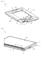
- the illumination device 1 of the present embodiment is provided with: a light source part 3 that has a planar light emitting panel 2 using an organic EL element; and an attachment part 4 that is configured to be attachable/detachable to/from the light source part 3.
- the light source part 3 is provided with: a cover 5 that is provided on a light emitting surface side of the light emitting panel 2 (lower direction in Fig. 1 ), allows light to exit, and has translucency; and a case 6 that is provided on a non-light emitting surface side of the light emitting panel 2 (upper direction in Fig. 1 ) and retains the cover 5.
- the cover 5 and case 6 constitute a package 7 of the light source part 3.
- the light emitting panel 2 and a wiring board 8 that is placed on the non-light emitting surface side of the light emitting panel 2 are contained.
- the attachment part 4 is provided with: a circuit board 9 for controlling lighting of the light emitting panel 2; and a housing 40 that contains the circuit board 9.
- the light emitting panel 2 is one configured such that, on a rectangular substrate having translucency, a light emitting part (not illustrated) is formed in which a positive electrode substantially consisting of a transparent conductive film, a light emitting layer having light emitting capability, and a negative electrode having light reflectivity are sequentially stacked, and the outside of the light emitting part is covered by a sealing material.
- a positive electrode substantially consisting of a transparent conductive film, a light emitting layer having light emitting capability, and a negative electrode having light reflectivity are sequentially stacked, and the outside of the light emitting part is covered by a sealing material.
- a heat equalizing plate including a copper plate and the like is provided.
- the wiring board 8 is a member formed in a frame shape so as to open the center with use of a base material having both fire retardancy and low electrical conductivity, i.e., a glass fiber plate formed by impregnating glass fiber cloth with epoxy resin or the like and curing the cloth, such as FR-4 (see Fig. 2 ).
- the wiring board 8 is, on a surface thereof facing to the case 6, provided with a terminal part 80 that makes an electrical connection between the wiring board 8 and the circuit board 9 of the attachment part 4.
- the terminal part 80 is configured to include: a fixed part that is joined to the wiring board 8; and a flat blade type contact part that is provided upright from the fixed part through a connecting part. The contact part is exposed toward the attachment part 4 side through a groove part 60 formed in the case 6.
- a pair of terminal parts 80 is provided in one end part of the wiring board 8. Note that, in Fig. 2 , for convenience, only one of the terminal parts 80 is illustrated, and illustration of the other terminal part is omitted. Also, on the wiring board 8, positive and negative electrode lines (not illustrated) that are electrically connected to the terminal parts 80 are formed, and covered by an insulating material, and on a surface opposite to a surface facing to the light emitting panel 2, parts of them are exposed to form land parts 81.
- the land parts 81 are, through electrically conductive wires 21, connected to power supply electrodes 20 (see Fig. 1 ) that are electrically connected to positive and negative electrodes of the light emitting panel 2, respectively.
- the light emitting panel 2 and wiring board 8 are bonded and fixed to each other by double-sided acrylic adhesive tape including a core that is superior in heat resistance, moisture resistance, and stress relaxation performance, or the like.
- the case 6 is configured such that a peripheral part on a front surface side thereof is formed so as to protrude in a direction facing to the attachment part 4, which on a back surface side thereof, constitutes a concave wiring board containing part 61 that contains the wiring board 8.
- the wiring board containing part 61 is formed in a frame shape in which a concave part 62 is arranged in the center and a part surrounding the center is formed in a convex shape.
- the case 6 has a pair of engaging parts 63 in one end part on a non-light emitting surface side thereof. The engaging parts 63 engage with engaged parts 41 that are provided on an attachment surface 4A of the attachment part 4, on which the light source part 3 is attached (see Fig. 3 ).
- the engaging parts 63 are formed in a hook shape of which a fore end faces outward, and the engaged parts 41 are formed in a shape corresponding to the shape of the engaging parts 63.
- the light source part 3 is adapted to be rotationally movable with respect to the attachment part 4.
- the rotational movement means that the light source part 3 uses one end side thereof as an axis to rotationally move the other end side with respect to the attachment part 4.
- the case 6 has a retaining part 64 (see Fig. 1 again) in a part on the non-light emitting surface side thereof, which is different from the one end part provided with the engaging parts 63, specifically, on the other side opposite to the one end part.
- the retaining part 64 is retained by a retained part 42 that is provided on the attachment surface 4A of the attachment part 4.
- the retaining part 64 is, as with the engaging parts 63, formed in a hook shape of which a fore end faces outward, and the retained part 42 is formed in a shape corresponding to the shape of the retaining part 64.
- the retaining part 64 and retained part 42 retains the light source part 3 in a state where the light source part 3 is attached to the attachment part 4.
- the attachment part 4 is, in addition to the above-described circuit board 9 and housing 40, provided with a pair of terminal receiving parts 43 that make electrical connections between the terminal parts 80 and the circuit board 9.
- the housing 40 is formed concavely on the light source part 3 side to constitute a concave circuit board containing part 44 that contains the circuit board 9. Also, the housing 40 is provided with through-grooves 45 respectively for inserting the terminal parts 80.
- a protecting member 90 for protecting the circuit board 9 is placed on the circuit board 9.
- circuit board 9 a base material similar to that of the wiring board 8 is used, and on a surface on the light source part 3 side of the base material that is formed in a rectangular shape, various elements (not illustrated) such as a driver for driving lighting of the light emitting panel 2 are mounted. Also, the circuit board 9 is provided with: junction parts with the terminal receiving parts 43; and external power supply terminals 91, and the junction parts, external power supply terminals 91, driver, and the like are electrically connected through a wiring pattern provided on the circuit board 9.
- the terminal receiving parts 43 are a pair of substantially L-shaped metal pieces that are bent into a predetermined shape, of which one end parts are fixed to the circuit board 9, and the other end parts are provided upright toward the light source part 3 side to form contact parts, and the contact parts are formed in a clip shape to hold, together with the through-grooves 45, the terminal parts 80 inserted into the through-grooves 45, respectively. This enables electrical connections between the terminal receiving parts 43 and the terminal parts 80 to be ensured.
- the circuit board containing part 44 is, to be fitted into the concave part 62 of the case 6, formed so as to be positioned in the center of the attachment part 4.
- screw locking parts 46 are provided in the circuit board containing part 44.
- a retaining frame 47 is provided on a peripheral edge of the circuit board containing part 44.
- the retaining frame 47 retains the circuit board 9 in a floating state together with the screw locking parts 46 so as to prevent the various elements mounted on the circuit board 9 from coming into contact with a bottom surface of the circuit board containing part 44.
- screw holes 92 are formed at positions corresponding to the screw locking parts 46 of the circuit board containing part 44. Screws are inserted into the screw holes 92 and screw locking parts 46 to thereby fix the circuit board 9 to the housing 40.
- the above-described engaged parts 41 and retained part 42 are provided on a surface of the housing 40, which faces to the light source part 3.
- the engaged parts 41 and retained part 42 are provided in locations corresponding to the engaging parts 63 and retaining part 64, respectively.
- the engaged parts 41 are slidably attached to the housing 40, and also biased toward the center of the attachment part 4 by biasing mechanisms such as springs, respectively.
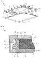
- the cover 5 is formed in a box shape of which a surface on the case 6 side is opened, and has: a light exit surface 5a that allows light from the light emitting panel 2 to exit; and a side wall 5b that is provided upright from an outer peripheral edge of the light exit surface 5a and covers an outer peripheral surface 2a of the light emitting panel 2.
- the light exit surface 5a is a surface that faces to a space irradiated with light from the illumination device 1.
- the side wall 5b is formed such that an inner peripheral surface 5d thereof fits the outer peripheral surface 2a of the light emitting panel 2. If so, only by fitting the light emitting panel 2 into the cover 5, the light emitting panel 2 and the wiring board 8 can be easily positioned.
- the side wall 5b of the cover 5 has, on an outer peripheral surface thereof, a plurality of fitting claws 5c for engaging the cover 5 with the case 6.
- the fitting claws 5c are formed so as to protrude toward an outer peripheral direction of the light exit surface 5a, and provided on the outer peripheral surface of the side wall 5b at predetermined intervals.
- a transparent plastic material such as ABS resin, acrylic resin, or polystyrene resin, or the like is used.
- the case 6 is formed in a box shape of which a surface on the cover 5 side is opened. Also, the case 6 has: a concave main surface 6a; and a side wall 6b that is provided upright from an outer peripheral edge of the main surface 6a and covers an outer periphery of the side wall 5b of the cover 5.
- the main surface 6a is a surface that constitutes the above-described wiring board containing part 61 and concave part 62.
- the side wall 6b has, on an inner peripheral surface thereof, a plurality of fitting grooves 6c into which the plurality of fitting claws 5c are fitted.
- the fitting grooves 6c are, on the side wall 6b, provided in locations corresponding to the fitting claws 5c.
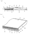
- the fitting claws 5c are provided with being displaced toward a light exit side rather than toward a fore end 5e of the side wall 5b, and the fitting grooves 6c are also provided in the locations corresponding to the fitting claws 5c. If so, at the time of assembling the package 7, the side wall 6b of the case 6 easily bends to smoothly fit the fitting claws 5c and the fitting grooves 6c into each other, and therefore the package 7 can be easily assembled. Also, in Fig.
- a length A from a lower end 5f of the side wall 5b to lower ends of the fitting claws 5c is short, i.e., as the fitting grooves 6c are displaced toward the light exit side, the side wall 6b is more easily bent; however, retaining strength of the fitting grooves 6c is reduced. Accordingly, the length A is appropriately set in consideration of strength of the material constituting the cover 5; however, if the length A is approximately 1 mm, strength of the cover 5 can be sufficiently kept. Also, a length B from the fore end 5e of the side wall 5b to upper ends of the fitting claws 5c is set such that when the cover 5 is temporarily inserted into the case 6 (see Fig. 6 ), the terminal parts 80 are temporarily retained in locations to be inserted into the groove parts 60 of the case 6, and also set so as to correspond to a depth of the case 6.
- a material having no transparency such as a metal material such as aluminum having a surface applied with insulation treatment may be used, and a material that has predetermined elasticity so as to slightly bend the side wall 6b is preferably used.
- a corner part that connects the main surface 6a and side wall 6b of the case 6 to each other is, as in the illustration, preferably partially chamfered. If so, an appearance of the light source part 3 can be slimmed.
- any shapes depending on the intended use of the illumination device 1 are used, and the cover 5 and case 6 are formed in shapes corresponding to a shape of the light emitting panel 2; however, in the present embodiment, the shapes are set as long-sized rectangular shapes as illustrated in the diagram.
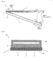
- a procedure for fitting the cover 5 into the case 6 is described referring to Fig. 7 in addition to above-described Fig. 6 .
- the case 6 is arranged on the cover 5 on which the light emitting panel 2 and wiring board 8 are preliminarily placed.
- a fore end of the side wall 6b of the case 6 is brought into a state of riding on the fitting claws 5c of the cover 5.
- pushing the case 6 toward the cover 5 side causes the inner peripheral surface of the side wall 6b of the case 6 to come into contact with the fitting claws 5c of the cover 5, and thereby the side wall 6b is pressed toward an outer peripheral direction of the main surface 6a.
- the side wall 6b of the case 6 is elastically deformed, but the side wall 5b of the cover 5 is not deformed, so that between the inner peripheral surface 5d of the side wall 5b of the cover 5 and the light emitting panel 2, it is not necessary to provide any gap, which enables a peripheral frame part of the light emitting panel 2 to be made smaller, and when a plurality of illumination devices 1 are provided together, an area of a light emitting surface as a whole can be increased.
- the light exit surface 5a of the cover 5, and the side wall 6b of the case 6, which is continuous with the light exit surface 5a are set to be on the same plane. If doing so, unevenness is not formed on the light exit surface 5a side of the light source part 3, and therefore an appearance as a design can be improved.
- the inner peripheral surface of the side wall 5b of the cover 5 fits the outer peripheral surface of the light emitting panel 2, and therefore the light emitting panel 2 and cover 5 are positioned in a state where the light emitting panel 2 is fitted into the cover 5.
- the terminal parts 80 penetrate through the groove parts 60 to protrude from the case 6. Accordingly, at the time of assembling the light source part 3, the terminal parts 80 are unlikely to be damaged, for example, the terminal parts 80 are brought into contact with the case 6 and thereby folded, or another damage, and therefore assembling work can be made efficient.
- Step 1 the user fits the engaging parts 63 of the light source part 3 into the engaged parts 41 of the attachment part 4 to engage them with each other.
- Step 2 the user pushes the light source part 3 toward a direction indicated by an arrow A1.
- the engaged parts 41 slide in a direction indicated by an arrow A2.
- Step 3 if the user lifts up an end part on the retaining part 64 side of the light source part 3 toward the attachment part 4 side, and also reduces pushing force toward the direction indicated by the arrow A2, the retaining part 64 is retained by the retained part 42 by biasing force of the engaged parts 41.
- the light source part 3 is attached to the attachment part 4.
- the retaining part 64 retains the retained part 42 and at the same time the terminal parts 80 are inserted into the terminal receiving parts 43 to thereby electrically connect the wiring board 8 and circuit board 9 (see Fig. 1 ) to each other.
- the light source part 3 is attached to the attachment part 4, and also the electrically connect is made to thereby realize a function as the illumination device 1.
- the side surfaces of the cover 5 are covered by the case 6, so that when the light emitting panel 2 is lit, the light from the light emitting panel 2 is unlikely to exit from the side surfaces of the cover 5, and thereby light toward lateral directions of the light source part 3 can be suppressed from leaking.
- the present invention is not limited to the configuration of the above-described embodiment, but can be variously modified without departing from the scope thereof.
- the depth of the case 6 is set to be slightly larger than thicknesses of the light emitting panel 2 and the cover 5, and between the case 6 and the light emitting panel 2, a gap adjustment member or the like for filing the gap may be provided.
Abstract
Description
- The present invention relates to an illumination device using an EL element for a light source.
- Organic EL elements can emit high luminance light with low voltage;< obtain various emission colors depending on the type of an organic compound; and be easily manufactured as planar light emitting panels. For these reasons, in recent years, a light emitting device provided with a light emitting panel using an organic EL element has attracted attention.
- However, in order to increase an area of an organic light emitting layer of the light emitting panel, a large-scale facility and the like are required to increase cost. Also, in the organic light emitting layer having a large area, it is not easy to uniform a luminance distribution. For these reasons, this sort of light emitting device is incorporated in an illumination device in a state where a plurality of light emitting devices each having a size of, for example, around 10 cm square are arranged together, and thereby a large light emitting area is achieved (see, for example, Patent Literature 1).
- Such a light emitting device is, in order to protect the organic light emitting layer of the light emitting panel from external damage, moisture, or the like, packaged by a cover having a translucent part or a predetermined case. This sort of illumination device is illustrated in
Fig. 9 . Theillumination device 101 is provided with: acover 102 that has translucency and allows light to exit; alight emitting device 103 that is arranged such that a light emitting surface faces to thecover 102; and acase 104 that is provided so as to cover an outer periphery and non-light emitting surface of thelight emitting device 103. - [Patent Literature 1]
JPA 2007-200627 - In the
illumination device 101 as described above, side surfaces of thecover 102 are exposed outside, so that light from thelight emitting device 103 is guided in thecover 102, and part of the light leaks from the side surfaces of thecover 102. That is, the part of the light exits in lateral directions of theillumination device 101 as well, and therefore an amount of light exiting in a front direction of thecover 102 is reduced by an amount equal to the leakage to deteriorate light use efficiency. Also, if, in the case where a plurality of light emitting devices are arranged together, light leaks in lateral directions of each of the light emitting devices, an appearance does not look good. Above-describedPatent Literature 1 discloses a configuration in which a plurality of light emitting devices are arranged together in a state of not being contained in a case or the like; however, in order to put the light emitting device into practical use as an illumination device, a case or the like is required. However, if the case or the like has a configuration as illustrated in aboveFig. 9 , after all, light leaks in lateral directions of the illumination device. - The present invention is made in order to solve the above problem, and an object thereof is to provide an illumination device that can suppress light from leaking in lateral directions.
- An illumination device of the present invention, which is provided with a planar light emitting panel, is provided with: a cover that is provided on a light emitting surface side of the light emitting panel, allows light to exit, and has translucency; and a case that is provided on a non-light emitting surface side of the light emitting panel and retains the cover, wherein: the cover has a side wall that covers an outer peripheral surface of the light emitting panel; the case has a side wall that covers an outer periphery of the side wall of the cover; the side wall of the cover is fitted into and retained by the side wall of the case; and side surfaces of the cover are covered by the case.
- In the illumination device, preferably, the side wall of the cover has, on an outer peripheral surface thereof, a plurality of fitting claws; the side wall of the case has, on an inner peripheral surface thereof, a plurality of fitting grooves that are to be fitted into with the plurality of fitting claws: and the fitting claws are provided with being displaced toward a light exit side rather than toward a fore end of the side wall of the cover.
- In the illumination device, preferably, an inner peripheral surface of the side wall of the cover is formed to fit the outer peripheral surface of the light emitting panel.
- In the illumination device, preferably, the cover has a light exit surface that allows light from the light emitting panel to exit; and the light exit surface and the side wall of the case are on a same plane, the side wall being continuous with the light exit surface.
- In the illumination device, preferably, the side wall of the case is elastically deformed, and thereby the fitting claws get over the inner peripheral surface of the side wall of the case, and are fitted into the fitting grooves.
- According to the illumination device according to the present invention, the side wall of the cover is fitted into and retained by the side wall of the case, so that the side surfaces of the cover are covered by the case and thereby light can be prevented from leaking in lateral directions of a light source part.
-
- [
Fig. 1] Fig. 1 is an exploded perspective view of an illumination device according to one embodiment of the present invention. - [
Fig. 2] Fig. 2 is a partial exploded perspective view of a light source part that the illumination device is provided with. - [
Fig. 3] Fig. 3 is a cross-sectional perspective view of the illumination device. - [
Fig. 4] Fig. 4 is an exploded perspective view of a cover and case that the light source part of the illumination device is provided with. - [
Fig. 5] Fig. 5 is a schematic side cross-sectional view at the time when the cover is fitted into the case. - [
Fig. 6] Fig. 6 is a partial exploded side view for explaining a procedure for fitting the cover into the case. - [
Fig. 7] Fig. 7 is a cross-sectional perspective view of the light source part. - [
Fig. 8] Fig. 8 is a side view for explaining steps of attaching the light source part to an attachment part in the illumination device. - [
Fig. 9] Fig. 9 is a side cross-sectional view of a conventional illumination device. - An illumination device according to one embodiment of the present invention is described referring to
Figs. 1 to 7 . As illustrated inFigs. 1 to 3 , theillumination device 1 of the present embodiment is provided with: alight source part 3 that has a planarlight emitting panel 2 using an organic EL element; and anattachment part 4 that is configured to be attachable/detachable to/from thelight source part 3. Thelight source part 3 is provided with: acover 5 that is provided on a light emitting surface side of the light emitting panel 2 (lower direction inFig. 1 ), allows light to exit, and has translucency; and acase 6 that is provided on a non-light emitting surface side of the light emitting panel 2 (upper direction inFig. 1 ) and retains thecover 5. Thecover 5 andcase 6 constitute apackage 7 of thelight source part 3. In thepackage 7, thelight emitting panel 2, and awiring board 8 that is placed on the non-light emitting surface side of thelight emitting panel 2 are contained. Theattachment part 4 is provided with: acircuit board 9 for controlling lighting of thelight emitting panel 2; and ahousing 40 that contains thecircuit board 9. - The
light emitting panel 2 is one configured such that, on a rectangular substrate having translucency, a light emitting part (not illustrated) is formed in which a positive electrode substantially consisting of a transparent conductive film, a light emitting layer having light emitting capability, and a negative electrode having light reflectivity are sequentially stacked, and the outside of the light emitting part is covered by a sealing material. For the substrate, positive electrode, light emitting layer, negative electrode, and sealing material, materials generally used for an organic EL element are appropriately used. Also, on the sealing material, a heat equalizing plate including a copper plate and the like is provided. - The
wiring board 8 is a member formed in a frame shape so as to open the center with use of a base material having both fire retardancy and low electrical conductivity, i.e., a glass fiber plate formed by impregnating glass fiber cloth with epoxy resin or the like and curing the cloth, such as FR-4 (seeFig. 2 ). Thewiring board 8 is, on a surface thereof facing to thecase 6, provided with aterminal part 80 that makes an electrical connection between thewiring board 8 and thecircuit board 9 of theattachment part 4. Theterminal part 80 is configured to include: a fixed part that is joined to thewiring board 8; and a flat blade type contact part that is provided upright from the fixed part through a connecting part. The contact part is exposed toward theattachment part 4 side through agroove part 60 formed in thecase 6. In the present embodiment, a pair ofterminal parts 80 is provided in one end part of thewiring board 8. Note that, inFig. 2 , for convenience, only one of theterminal parts 80 is illustrated, and illustration of the other terminal part is omitted. Also, on thewiring board 8, positive and negative electrode lines (not illustrated) that are electrically connected to theterminal parts 80 are formed, and covered by an insulating material, and on a surface opposite to a surface facing to thelight emitting panel 2, parts of them are exposed toform land parts 81. Theland parts 81 are, through electricallyconductive wires 21, connected to power supply electrodes 20 (seeFig. 1 ) that are electrically connected to positive and negative electrodes of thelight emitting panel 2, respectively. Thelight emitting panel 2 andwiring board 8 are bonded and fixed to each other by double-sided acrylic adhesive tape including a core that is superior in heat resistance, moisture resistance, and stress relaxation performance, or the like. - The
case 6 is configured such that a peripheral part on a front surface side thereof is formed so as to protrude in a direction facing to theattachment part 4, which on a back surface side thereof, constitutes a concave wiringboard containing part 61 that contains thewiring board 8. The wiringboard containing part 61 is formed in a frame shape in which aconcave part 62 is arranged in the center and a part surrounding the center is formed in a convex shape. Also, thecase 6 has a pair ofengaging parts 63 in one end part on a non-light emitting surface side thereof. Theengaging parts 63 engage with engagedparts 41 that are provided on anattachment surface 4A of theattachment part 4, on which thelight source part 3 is attached (seeFig. 3 ). Theengaging parts 63 are formed in a hook shape of which a fore end faces outward, and the engagedparts 41 are formed in a shape corresponding to the shape of theengaging parts 63. In a state where theengaging parts 63 are respectively engaged with the engagedparts 41, thelight source part 3 is adapted to be rotationally movable with respect to theattachment part 4. The rotational movement means that thelight source part 3 uses one end side thereof as an axis to rotationally move the other end side with respect to theattachment part 4. - Also, the
case 6 has a retaining part 64 (seeFig. 1 again) in a part on the non-light emitting surface side thereof, which is different from the one end part provided with theengaging parts 63, specifically, on the other side opposite to the one end part. The retainingpart 64 is retained by a retainedpart 42 that is provided on theattachment surface 4A of theattachment part 4. The retainingpart 64 is, as with the engagingparts 63, formed in a hook shape of which a fore end faces outward, and the retainedpart 42 is formed in a shape corresponding to the shape of the retainingpart 64. The retainingpart 64 and retainedpart 42 retains thelight source part 3 in a state where thelight source part 3 is attached to theattachment part 4. - The
attachment part 4 is, in addition to the above-describedcircuit board 9 andhousing 40, provided with a pair ofterminal receiving parts 43 that make electrical connections between theterminal parts 80 and thecircuit board 9. Thehousing 40 is formed concavely on thelight source part 3 side to constitute a concave circuitboard containing part 44 that contains thecircuit board 9. Also, thehousing 40 is provided with through-grooves 45 respectively for inserting theterminal parts 80. In addition, on thecircuit board 9, a protectingmember 90 for protecting thecircuit board 9 is placed. - For the
circuit board 9, a base material similar to that of thewiring board 8 is used, and on a surface on thelight source part 3 side of the base material that is formed in a rectangular shape, various elements (not illustrated) such as a driver for driving lighting of thelight emitting panel 2 are mounted. Also, thecircuit board 9 is provided with: junction parts with theterminal receiving parts 43; and externalpower supply terminals 91, and the junction parts, externalpower supply terminals 91, driver, and the like are electrically connected through a wiring pattern provided on thecircuit board 9. Theterminal receiving parts 43 are a pair of substantially L-shaped metal pieces that are bent into a predetermined shape, of which one end parts are fixed to thecircuit board 9, and the other end parts are provided upright toward thelight source part 3 side to form contact parts, and the contact parts are formed in a clip shape to hold, together with the through-grooves 45, theterminal parts 80 inserted into the through-grooves 45, respectively. This enables electrical connections between theterminal receiving parts 43 and theterminal parts 80 to be ensured. - The circuit
board containing part 44 is, to be fitted into theconcave part 62 of thecase 6, formed so as to be positioned in the center of theattachment part 4. In the circuitboard containing part 44,screw locking parts 46 are provided. Also, on a peripheral edge of the circuitboard containing part 44, a retainingframe 47 is provided. The retainingframe 47 retains thecircuit board 9 in a floating state together with thescrew locking parts 46 so as to prevent the various elements mounted on thecircuit board 9 from coming into contact with a bottom surface of the circuitboard containing part 44. In thecircuit board 9, screw holes 92 are formed at positions corresponding to thescrew locking parts 46 of the circuitboard containing part 44. Screws are inserted into the screw holes 92 andscrew locking parts 46 to thereby fix thecircuit board 9 to thehousing 40. - In addition, in the
attachment part 4, on a surface of thehousing 40, which faces to thelight source part 3, the above-described engagedparts 41 and retainedpart 42 are provided. The engagedparts 41 and retainedpart 42 are provided in locations corresponding to the engagingparts 63 and retainingpart 64, respectively. Also, the engagedparts 41 are slidably attached to thehousing 40, and also biased toward the center of theattachment part 4 by biasing mechanisms such as springs, respectively. - Next, the
cover 5 andcase 6 that constitute thepackage 7 are described in detail referring toFigs. 4 to 6 . Note that, inFig. 5 , illustration of a partial configuration of thelight source part 3, such as thewiring board 8, is omitted. Also, in the same diagram, for descriptive convenience, a gap between thecover 5 and thecase 6 is largely illustrated. - The
cover 5 is formed in a box shape of which a surface on thecase 6 side is opened, and has: alight exit surface 5a that allows light from thelight emitting panel 2 to exit; and aside wall 5b that is provided upright from an outer peripheral edge of thelight exit surface 5a and covers an outerperipheral surface 2a of thelight emitting panel 2. Thelight exit surface 5a is a surface that faces to a space irradiated with light from theillumination device 1. Theside wall 5b is formed such that an innerperipheral surface 5d thereof fits the outerperipheral surface 2a of thelight emitting panel 2. If so, only by fitting thelight emitting panel 2 into thecover 5, thelight emitting panel 2 and thewiring board 8 can be easily positioned. - The
side wall 5b of thecover 5 has, on an outer peripheral surface thereof, a plurality offitting claws 5c for engaging thecover 5 with thecase 6. Thefitting claws 5c are formed so as to protrude toward an outer peripheral direction of thelight exit surface 5a, and provided on the outer peripheral surface of theside wall 5b at predetermined intervals. As a constituent material of thecover 5, for example, a transparent plastic material such as ABS resin, acrylic resin, or polystyrene resin, or the like is used. - The
case 6 is formed in a box shape of which a surface on thecover 5 side is opened. Also, thecase 6 has: a concavemain surface 6a; and aside wall 6b that is provided upright from an outer peripheral edge of themain surface 6a and covers an outer periphery of theside wall 5b of thecover 5. Themain surface 6a is a surface that constitutes the above-described wiringboard containing part 61 andconcave part 62. Also, theside wall 6b has, on an inner peripheral surface thereof, a plurality offitting grooves 6c into which the plurality offitting claws 5c are fitted. Thefitting grooves 6c are, on theside wall 6b, provided in locations corresponding to thefitting claws 5c. - Also, the
fitting claws 5c are provided with being displaced toward a light exit side rather than toward afore end 5e of theside wall 5b, and thefitting grooves 6c are also provided in the locations corresponding to thefitting claws 5c. If so, at the time of assembling thepackage 7, theside wall 6b of thecase 6 easily bends to smoothly fit thefitting claws 5c and thefitting grooves 6c into each other, and therefore thepackage 7 can be easily assembled. Also, inFig. 5 , a length A from alower end 5f of theside wall 5b to lower ends of thefitting claws 5c is short, i.e., as thefitting grooves 6c are displaced toward the light exit side, theside wall 6b is more easily bent; however, retaining strength of thefitting grooves 6c is reduced. Accordingly, the length A is appropriately set in consideration of strength of the material constituting thecover 5; however, if the length A is approximately 1 mm, strength of thecover 5 can be sufficiently kept. Also, a length B from thefore end 5e of theside wall 5b to upper ends of thefitting claws 5c is set such that when thecover 5 is temporarily inserted into the case 6 (seeFig. 6 ), theterminal parts 80 are temporarily retained in locations to be inserted into thegroove parts 60 of thecase 6, and also set so as to correspond to a depth of thecase 6. - As a constituent material of the
case 6, in addition to the same one as the constituent material of thecover 5, a material having no transparency such as a metal material such as aluminum having a surface applied with insulation treatment may be used, and a material that has predetermined elasticity so as to slightly bend theside wall 6b is preferably used. In addition, a corner part that connects themain surface 6a andside wall 6b of thecase 6 to each other is, as in the illustration, preferably partially chamfered. If so, an appearance of thelight source part 3 can be slimmed. Also, as shapes of thecover 5 andcase 6 that constitute thepackage 7, any shapes depending on the intended use of theillumination device 1 are used, and thecover 5 andcase 6 are formed in shapes corresponding to a shape of thelight emitting panel 2; however, in the present embodiment, the shapes are set as long-sized rectangular shapes as illustrated in the diagram. - Next, a procedure for fitting the
cover 5 into thecase 6 is described referring toFig. 7 in addition to above-describedFig. 6 . As illustrated inFig. 6 , thecase 6 is arranged on thecover 5 on which thelight emitting panel 2 andwiring board 8 are preliminarily placed. At this time, a fore end of theside wall 6b of thecase 6 is brought into a state of riding on thefitting claws 5c of thecover 5. Then, pushing thecase 6 toward thecover 5 side causes the inner peripheral surface of theside wall 6b of thecase 6 to come into contact with thefitting claws 5c of thecover 5, and thereby theside wall 6b is pressed toward an outer peripheral direction of themain surface 6a. Subsequently, further pushing thecase 6 toward thecover 5 side causes theside wall 6b of thecase 6 to be elastically deformed, so that thefitting claws 5c get over the inner peripheral surface of theside wall 6b of thecase 6, and are fitted into and retained by thefitting grooves 6c, and also side surfaces of thecover 5 are covered by thecase 6. If doing so, thefitting claws 5c are smoothly fitted into thefitting grooves 6c, and thereby thepackage 7 can be easily assembled. Also, theside wall 6b of thecase 6 is elastically deformed, but theside wall 5b of thecover 5 is not deformed, so that between the innerperipheral surface 5d of theside wall 5b of thecover 5 and thelight emitting panel 2, it is not necessary to provide any gap, which enables a peripheral frame part of thelight emitting panel 2 to be made smaller, and when a plurality ofillumination devices 1 are provided together, an area of a light emitting surface as a whole can be increased. - Also, as illustrated in
Fig. 7 , it is preferable that, in a state where thecase 6 andcover 5 are fitted into each other, thelight exit surface 5a of thecover 5, and theside wall 6b of thecase 6, which is continuous with thelight exit surface 5a, are set to be on the same plane. If doing so, unevenness is not formed on thelight exit surface 5a side of thelight source part 3, and therefore an appearance as a design can be improved. - Also, the inner peripheral surface of the
side wall 5b of thecover 5 fits the outer peripheral surface of thelight emitting panel 2, and therefore thelight emitting panel 2 andcover 5 are positioned in a state where thelight emitting panel 2 is fitted into thecover 5. For this reason, only by fitting thecover 5 andcase 6 into each other, theterminal parts 80 penetrate through thegroove parts 60 to protrude from thecase 6. Accordingly, at the time of assembling thelight source part 3, theterminal parts 80 are unlikely to be damaged, for example, theterminal parts 80 are brought into contact with thecase 6 and thereby folded, or another damage, and therefore assembling work can be made efficient. - The assembled
light source part 3 is attached to theattachment part 4 that is preliminarily installed on a wall surface or the like. Here, a procedure ofSteps 1 to 3 in which a user attaches thelight source part 3 to theattachment part 4 is described referring toFig. 8 . InStep 1, the user fits the engagingparts 63 of thelight source part 3 into the engagedparts 41 of theattachment part 4 to engage them with each other. InStep 2, the user pushes thelight source part 3 toward a direction indicated by an arrow A1. In response to this, the engagedparts 41 slide in a direction indicated by an arrow A2. InStep 3, if the user lifts up an end part on the retainingpart 64 side of thelight source part 3 toward theattachment part 4 side, and also reduces pushing force toward the direction indicated by the arrow A2, the retainingpart 64 is retained by the retainedpart 42 by biasing force of the engagedparts 41. In the above procedure, thelight source part 3 is attached to theattachment part 4. In this configuration, the retainingpart 64 retains the retainedpart 42 and at the same time theterminal parts 80 are inserted into theterminal receiving parts 43 to thereby electrically connect thewiring board 8 and circuit board 9 (seeFig. 1 ) to each other. In this manner, thelight source part 3 is attached to theattachment part 4, and also the electrically connect is made to thereby realize a function as theillumination device 1. - According to the
illumination device 1, as described above, the side surfaces of thecover 5 are covered by thecase 6, so that when thelight emitting panel 2 is lit, the light from thelight emitting panel 2 is unlikely to exit from the side surfaces of thecover 5, and thereby light toward lateral directions of thelight source part 3 can be suppressed from leaking. - In the case of detaching the
light source part 3 from theattachment part 4, if the user slides thelight source part 3 in the direction indicated by the arrow A2 inFig. 8 , the retention between the retainingpart 64 and the retainedpart 42 is released, and therefore pulling out thelight source part 3 in a direction opposite to the direction indicated by the arrow A2 causes the engagement between the engagingparts 63 and the engagedparts 41 to be released. In the case where a plurality ofillumination devices 1 are arranged in a grid form, by inserting a rod-like member between any adjacent two of theillumination devices 1, the engagedparts 41 are slid. By doing so, in the same manner as that described above, thelight source parts 3 slightly slide, and the retainingparts 64 are removed from the retainedparts 42 and no longer retained, so that thelight source parts 3 can be detached from theattachment parts 4, respectively. - The present invention is not limited to the configuration of the above-described embodiment, but can be variously modified without departing from the scope thereof. For example, the depth of the
case 6 is set to be slightly larger than thicknesses of thelight emitting panel 2 and thecover 5, and between thecase 6 and thelight emitting panel 2, a gap adjustment member or the like for filing the gap may be provided. -
- 1:
- Illumination device
- 2:
- Light emitting panel
- 2a:
- Outer peripheral surface
- 5:
- Cover
- 5a:
- Light exit surface
- 5b:
- Side wall
- 5c:
- Fitting claw
- 5d:
- Inner peripheral surface
- 5e:
- Fore end
- 6:
- Case
- 6b:
- Side wall
- 6c:
- Fitting groove
Claims (5)
- An illumination device provided with a planar light emitting panel, the illumination device comprising:a cover that is provided on a light emitting surface side of the light emitting panel, allows light to exit, and has translucency; anda case that is provided on a non-light emitting surface side of the light emitting panel and retains the cover, wherein:the cover has a side wall that covers an outer peripheral surface of the light emitting panel;the case has a side wall that covers an outer periphery of the side wall of the cover;the side wall of the cover is fitted into and retained by the side wall of the case; andside surfaces of the cover are covered by the case.
- The illumination device according to claim 1, wherein:the side wall of the cover has, on an outer peripheral surface thereof, a plurality of fitting claws;the side wall of the case has, on an inner peripheral surface thereof, a plurality of fitting grooves that are to be fitted into with the plurality of fitting claws: andthe fitting claws are provided with being displaced toward a light exit side rather than toward a fore end of the side wall of the cover.
- The illumination device according to claim 1 or 2, wherein
an inner peripheral surface of the side wall of the cover is formed to fit the outer peripheral surface of the light emitting panel. - The illumination device according to any one of claims 1 to 3, wherein:the cover has a light exit surface that allows light from the light emitting panel to exit; andthe light exit surface and the side wall of the case are on a same plane, the side wall being continuous with the light exit surface.
- The illumination device according to claim 2, wherein
the side wall of the case is elastically deformed, and thereby the fitting claws get over the inner peripheral surface of the side wall of the case, and are fitted into the fitting grooves.
Applications Claiming Priority (1)
| Application Number | Priority Date | Filing Date | Title |
|---|---|---|---|
| JP2011186905A JP5909668B2 (en) | 2011-08-30 | 2011-08-30 | Lighting device |
Publications (3)
| Publication Number | Publication Date |
|---|---|
| EP2565532A2 true EP2565532A2 (en) | 2013-03-06 |
| EP2565532A3 EP2565532A3 (en) | 2013-03-20 |
| EP2565532B1 EP2565532B1 (en) | 2014-12-24 |
Family
ID=46799094
Family Applications (1)
| Application Number | Title | Priority Date | Filing Date |
|---|---|---|---|
| EP12182287.8A Not-in-force EP2565532B1 (en) | 2011-08-30 | 2012-08-30 | Illumination device |
Country Status (2)
| Country | Link |
|---|---|
| EP (1) | EP2565532B1 (en) |
| JP (1) | JP5909668B2 (en) |
Cited By (4)
| Publication number | Priority date | Publication date | Assignee | Title |
|---|---|---|---|---|
| CH709411A1 (en) * | 2014-03-26 | 2015-09-30 | Ribag Licht Ag | Luminous element with Oled. |
| FR3056283A1 (en) * | 2016-09-21 | 2018-03-23 | Valeo Vision | LIGHT DEVICE COMPRISING A SURFACE LIGHT SOURCE |
| US20190104592A1 (en) * | 2016-04-28 | 2019-04-04 | Kilt Planning Office Inc. | Illumination device and attachment member |
| CN109716022A (en) * | 2016-09-22 | 2019-05-03 | 昕诺飞控股有限公司 | The box lamp support of core slot is caught in and grounding assembly |
Family Cites Families (11)
| Publication number | Priority date | Publication date | Assignee | Title |
|---|---|---|---|---|
| US5632551A (en) * | 1994-07-18 | 1997-05-27 | Grote Industries, Inc. | LED vehicle lamp assembly |
| JP4117979B2 (en) * | 1999-07-26 | 2008-07-16 | 三菱電機株式会社 | Liquid crystal display |
| JP2002182204A (en) * | 2000-12-12 | 2002-06-26 | Optrex Corp | Backlight for liquid crystal display element |
| TW572220U (en) * | 2003-01-08 | 2004-01-11 | Hannstar Display Corp | Liquid crystal display module and its fixing structure |
| US6967439B2 (en) * | 2004-02-24 | 2005-11-22 | Eastman Kodak Company | OLED display having thermally conductive backplate |
| JP4679922B2 (en) * | 2005-02-15 | 2011-05-11 | 小泉産業株式会社 | EL light source |
| DE102006001947A1 (en) * | 2005-09-12 | 2007-03-29 | Kompled Gmbh & Co. Kg | taillights arrangement |
| JP2007150162A (en) * | 2005-11-30 | 2007-06-14 | Konica Minolta Holdings Inc | Surface light emitting element |
| JP2007280693A (en) * | 2006-04-04 | 2007-10-25 | Koizumi Lighting Technology Corp | El light source |
| JP4867877B2 (en) * | 2007-09-21 | 2012-02-01 | パナソニック電工株式会社 | Surface-emitting light fixture |
| JP5451439B2 (en) * | 2010-02-10 | 2014-03-26 | Lumiotec株式会社 | Organic EL lighting device |
-
2011
- 2011-08-30 JP JP2011186905A patent/JP5909668B2/en active Active
-
2012
- 2012-08-30 EP EP12182287.8A patent/EP2565532B1/en not_active Not-in-force
Non-Patent Citations (1)
| Title |
|---|
| None |
Cited By (8)
| Publication number | Priority date | Publication date | Assignee | Title |
|---|---|---|---|---|
| CH709411A1 (en) * | 2014-03-26 | 2015-09-30 | Ribag Licht Ag | Luminous element with Oled. |
| US20190104592A1 (en) * | 2016-04-28 | 2019-04-04 | Kilt Planning Office Inc. | Illumination device and attachment member |
| US10683976B2 (en) * | 2016-04-28 | 2020-06-16 | Kilt Planning Office Inc. | Illumination device and attachment member |
| FR3056283A1 (en) * | 2016-09-21 | 2018-03-23 | Valeo Vision | LIGHT DEVICE COMPRISING A SURFACE LIGHT SOURCE |
| EP3299219A1 (en) * | 2016-09-21 | 2018-03-28 | Valeo Vision | Light device comprising an oled light source |
| CN107859966A (en) * | 2016-09-21 | 2018-03-30 | 法雷奥照明公司 | Lamp device including surface source of light |
| US10718480B2 (en) | 2016-09-21 | 2020-07-21 | Valeo Vision | Light device comprising a surface light source |
| CN109716022A (en) * | 2016-09-22 | 2019-05-03 | 昕诺飞控股有限公司 | The box lamp support of core slot is caught in and grounding assembly |
Also Published As
| Publication number | Publication date |
|---|---|
| EP2565532B1 (en) | 2014-12-24 |
| JP5909668B2 (en) | 2016-04-27 |
| EP2565532A3 (en) | 2013-03-20 |
| JP2013051046A (en) | 2013-03-14 |
Similar Documents
| Publication | Publication Date | Title |
|---|---|---|
| CN102410452B (en) | Lighting module and lighting apparatus including same | |
| EP2495492B1 (en) | Illumination device | |
| US9400095B2 (en) | Lighting apparatus | |
| KR101088715B1 (en) | LED lighting device and its manufacturing method | |
| TW201124671A (en) | Lighting device | |
| EP2830393A1 (en) | Organic el module and electricty supply structure for organic el module | |
| EP2565532A2 (en) | Illumination device | |
| EP2772957A1 (en) | Lighting device | |
| CN102889506A (en) | Light bar structure and light source device thereof | |
| US9812831B2 (en) | Connector for lighting devices and corresponding method | |
| EP2495491B1 (en) | Illumination device | |
| JP6277743B2 (en) | Waterproof case and waterproof guide light | |
| JP5105517B2 (en) | Surface emitting module | |
| JP2007287345A (en) | El light emitting module | |
| JP2020035724A (en) | Light source unit and display device including the same | |
| JP7308571B2 (en) | Fixtures, fixture sets and lighting fixtures using them | |
| JP7131865B2 (en) | Fixtures, fixture sets and lighting fixtures using them | |
| JP2013050520A (en) | Light emission device and illumination device | |
| KR101797487B1 (en) | Lighting module and lighting apparatus comprising the same | |
| CN205807320U (en) | A kind of chassis and illuminator | |
| JP2023115139A (en) | Fixture, fixture set and lighting fixture including the same | |
| KR101861149B1 (en) | Lighting apparatus | |
| JP5796200B2 (en) | Lighting device | |
| JP2014107121A (en) | Lighting device | |
| JP2014110134A (en) | Lighting device |
Legal Events
| Date | Code | Title | Description |
|---|---|---|---|
| PUAL | Search report despatched |
Free format text: ORIGINAL CODE: 0009013 |
|
| PUAI | Public reference made under article 153(3) epc to a published international application that has entered the european phase |
Free format text: ORIGINAL CODE: 0009012 |
|
| AK | Designated contracting states |
Kind code of ref document: A2 Designated state(s): AL AT BE BG CH CY CZ DE DK EE ES FI FR GB GR HR HU IE IS IT LI LT LU LV MC MK MT NL NO PL PT RO RS SE SI SK SM TR |
|
| AX | Request for extension of the european patent |
Extension state: BA ME |
|
| AK | Designated contracting states |
Kind code of ref document: A3 Designated state(s): AL AT BE BG CH CY CZ DE DK EE ES FI FR GB GR HR HU IE IS IT LI LT LU LV MC MK MT NL NO PL PT RO RS SE SI SK SM TR |
|
| AX | Request for extension of the european patent |
Extension state: BA ME |
|
| RIC1 | Information provided on ipc code assigned before grant |
Ipc: F21Y 105/00 20060101ALN20130213BHEP Ipc: F21V 15/01 20060101AFI20130213BHEP Ipc: F21V 17/16 20060101ALI20130213BHEP Ipc: H01L 51/52 20060101ALI20130213BHEP Ipc: F21S 8/04 20060101ALN20130213BHEP Ipc: F21V 21/02 20060101ALN20130213BHEP |
|
| 17P | Request for examination filed |
Effective date: 20130411 |
|
| 17Q | First examination report despatched |
Effective date: 20131106 |
|
| RIC1 | Information provided on ipc code assigned before grant |
Ipc: F21V 17/16 20060101ALI20140214BHEP Ipc: F21S 8/04 20060101ALN20140214BHEP Ipc: F21Y 105/00 20060101ALN20140214BHEP Ipc: F21V 15/01 20060101AFI20140214BHEP Ipc: H01L 51/52 20060101ALI20140214BHEP Ipc: F21V 21/02 20060101ALN20140214BHEP |
|
| RIC1 | Information provided on ipc code assigned before grant |
Ipc: F21V 21/02 20060101ALN20140327BHEP Ipc: H01L 51/52 20060101ALI20140327BHEP Ipc: F21V 15/01 20060101AFI20140327BHEP Ipc: F21Y 105/00 20060101ALN20140327BHEP Ipc: F21S 8/04 20060101ALN20140327BHEP Ipc: F21V 17/16 20060101ALI20140327BHEP |
|
| GRAP | Despatch of communication of intention to grant a patent |
Free format text: ORIGINAL CODE: EPIDOSNIGR1 |
|
| INTG | Intention to grant announced |
Effective date: 20140520 |
|
| GRAS | Grant fee paid |
Free format text: ORIGINAL CODE: EPIDOSNIGR3 |
|
| GRAA | (expected) grant |
Free format text: ORIGINAL CODE: 0009210 |
|
| AK | Designated contracting states |
Kind code of ref document: B1 Designated state(s): AL AT BE BG CH CY CZ DE DK EE ES FI FR GB GR HR HU IE IS IT LI LT LU LV MC MK MT NL NO PL PT RO RS SE SI SK SM TR |
|
| REG | Reference to a national code |
Ref country code: GB Ref legal event code: FG4D |
|
| REG | Reference to a national code |
Ref country code: CH Ref legal event code: EP |
|
| REG | Reference to a national code |
Ref country code: IE Ref legal event code: FG4D |
|
| REG | Reference to a national code |
Ref country code: AT Ref legal event code: REF Ref document number: 703354 Country of ref document: AT Kind code of ref document: T Effective date: 20150115 |
|
| REG | Reference to a national code |
Ref country code: DE Ref legal event code: R096 Ref document number: 602012004477 Country of ref document: DE Effective date: 20150219 |
|
| REG | Reference to a national code |
Ref country code: NL Ref legal event code: VDEP Effective date: 20141224 |
|
| PG25 | Lapsed in a contracting state [announced via postgrant information from national office to epo] |
Ref country code: NO Free format text: LAPSE BECAUSE OF FAILURE TO SUBMIT A TRANSLATION OF THE DESCRIPTION OR TO PAY THE FEE WITHIN THE PRESCRIBED TIME-LIMIT Effective date: 20150324 Ref country code: FI Free format text: LAPSE BECAUSE OF FAILURE TO SUBMIT A TRANSLATION OF THE DESCRIPTION OR TO PAY THE FEE WITHIN THE PRESCRIBED TIME-LIMIT Effective date: 20141224 Ref country code: LT Free format text: LAPSE BECAUSE OF FAILURE TO SUBMIT A TRANSLATION OF THE DESCRIPTION OR TO PAY THE FEE WITHIN THE PRESCRIBED TIME-LIMIT Effective date: 20141224 |
|
| REG | Reference to a national code |
Ref country code: LT Ref legal event code: MG4D |
|
| PG25 | Lapsed in a contracting state [announced via postgrant information from national office to epo] |
Ref country code: HR Free format text: LAPSE BECAUSE OF FAILURE TO SUBMIT A TRANSLATION OF THE DESCRIPTION OR TO PAY THE FEE WITHIN THE PRESCRIBED TIME-LIMIT Effective date: 20141224 Ref country code: LV Free format text: LAPSE BECAUSE OF FAILURE TO SUBMIT A TRANSLATION OF THE DESCRIPTION OR TO PAY THE FEE WITHIN THE PRESCRIBED TIME-LIMIT Effective date: 20141224 Ref country code: SE Free format text: LAPSE BECAUSE OF FAILURE TO SUBMIT A TRANSLATION OF THE DESCRIPTION OR TO PAY THE FEE WITHIN THE PRESCRIBED TIME-LIMIT Effective date: 20141224 Ref country code: GR Free format text: LAPSE BECAUSE OF FAILURE TO SUBMIT A TRANSLATION OF THE DESCRIPTION OR TO PAY THE FEE WITHIN THE PRESCRIBED TIME-LIMIT Effective date: 20150325 Ref country code: RS Free format text: LAPSE BECAUSE OF FAILURE TO SUBMIT A TRANSLATION OF THE DESCRIPTION OR TO PAY THE FEE WITHIN THE PRESCRIBED TIME-LIMIT Effective date: 20141224 |
|
| REG | Reference to a national code |
Ref country code: AT Ref legal event code: MK05 Ref document number: 703354 Country of ref document: AT Kind code of ref document: T Effective date: 20141224 |
|
| PG25 | Lapsed in a contracting state [announced via postgrant information from national office to epo] |
Ref country code: NL Free format text: LAPSE BECAUSE OF FAILURE TO SUBMIT A TRANSLATION OF THE DESCRIPTION OR TO PAY THE FEE WITHIN THE PRESCRIBED TIME-LIMIT Effective date: 20141224 |
|
| PG25 | Lapsed in a contracting state [announced via postgrant information from national office to epo] |
Ref country code: EE Free format text: LAPSE BECAUSE OF FAILURE TO SUBMIT A TRANSLATION OF THE DESCRIPTION OR TO PAY THE FEE WITHIN THE PRESCRIBED TIME-LIMIT Effective date: 20141224 Ref country code: ES Free format text: LAPSE BECAUSE OF FAILURE TO SUBMIT A TRANSLATION OF THE DESCRIPTION OR TO PAY THE FEE WITHIN THE PRESCRIBED TIME-LIMIT Effective date: 20141224 Ref country code: RO Free format text: LAPSE BECAUSE OF FAILURE TO SUBMIT A TRANSLATION OF THE DESCRIPTION OR TO PAY THE FEE WITHIN THE PRESCRIBED TIME-LIMIT Effective date: 20141224 Ref country code: SK Free format text: LAPSE BECAUSE OF FAILURE TO SUBMIT A TRANSLATION OF THE DESCRIPTION OR TO PAY THE FEE WITHIN THE PRESCRIBED TIME-LIMIT Effective date: 20141224 Ref country code: CZ Free format text: LAPSE BECAUSE OF FAILURE TO SUBMIT A TRANSLATION OF THE DESCRIPTION OR TO PAY THE FEE WITHIN THE PRESCRIBED TIME-LIMIT Effective date: 20141224 |
|
| PG25 | Lapsed in a contracting state [announced via postgrant information from national office to epo] |
Ref country code: AT Free format text: LAPSE BECAUSE OF FAILURE TO SUBMIT A TRANSLATION OF THE DESCRIPTION OR TO PAY THE FEE WITHIN THE PRESCRIBED TIME-LIMIT Effective date: 20141224 Ref country code: IS Free format text: LAPSE BECAUSE OF FAILURE TO SUBMIT A TRANSLATION OF THE DESCRIPTION OR TO PAY THE FEE WITHIN THE PRESCRIBED TIME-LIMIT Effective date: 20150424 Ref country code: PL Free format text: LAPSE BECAUSE OF FAILURE TO SUBMIT A TRANSLATION OF THE DESCRIPTION OR TO PAY THE FEE WITHIN THE PRESCRIBED TIME-LIMIT Effective date: 20141224 |
|
| REG | Reference to a national code |
Ref country code: DE Ref legal event code: R097 Ref document number: 602012004477 Country of ref document: DE |
|
| PG25 | Lapsed in a contracting state [announced via postgrant information from national office to epo] |
Ref country code: DK Free format text: LAPSE BECAUSE OF FAILURE TO SUBMIT A TRANSLATION OF THE DESCRIPTION OR TO PAY THE FEE WITHIN THE PRESCRIBED TIME-LIMIT Effective date: 20141224 |
|
| PLBE | No opposition filed within time limit |
Free format text: ORIGINAL CODE: 0009261 |
|
| STAA | Information on the status of an ep patent application or granted ep patent |
Free format text: STATUS: NO OPPOSITION FILED WITHIN TIME LIMIT |
|
| 26N | No opposition filed |
Effective date: 20150925 |
|
| PG25 | Lapsed in a contracting state [announced via postgrant information from national office to epo] |
Ref country code: IT Free format text: LAPSE BECAUSE OF FAILURE TO SUBMIT A TRANSLATION OF THE DESCRIPTION OR TO PAY THE FEE WITHIN THE PRESCRIBED TIME-LIMIT Effective date: 20141224 |
|
| PG25 | Lapsed in a contracting state [announced via postgrant information from national office to epo] |
Ref country code: SI Free format text: LAPSE BECAUSE OF FAILURE TO SUBMIT A TRANSLATION OF THE DESCRIPTION OR TO PAY THE FEE WITHIN THE PRESCRIBED TIME-LIMIT Effective date: 20141224 |
|
| PG25 | Lapsed in a contracting state [announced via postgrant information from national office to epo] |
Ref country code: MC Free format text: LAPSE BECAUSE OF FAILURE TO SUBMIT A TRANSLATION OF THE DESCRIPTION OR TO PAY THE FEE WITHIN THE PRESCRIBED TIME-LIMIT Effective date: 20141224 Ref country code: LU Free format text: LAPSE BECAUSE OF FAILURE TO SUBMIT A TRANSLATION OF THE DESCRIPTION OR TO PAY THE FEE WITHIN THE PRESCRIBED TIME-LIMIT Effective date: 20150830 |
|
| REG | Reference to a national code |
Ref country code: CH Ref legal event code: PL |
|
| PG25 | Lapsed in a contracting state [announced via postgrant information from national office to epo] |
Ref country code: CH Free format text: LAPSE BECAUSE OF NON-PAYMENT OF DUE FEES Effective date: 20150831 Ref country code: LI Free format text: LAPSE BECAUSE OF NON-PAYMENT OF DUE FEES Effective date: 20150831 |
|
| PG25 | Lapsed in a contracting state [announced via postgrant information from national office to epo] |
Ref country code: BE Free format text: LAPSE BECAUSE OF FAILURE TO SUBMIT A TRANSLATION OF THE DESCRIPTION OR TO PAY THE FEE WITHIN THE PRESCRIBED TIME-LIMIT Effective date: 20141224 |
|
| REG | Reference to a national code |
Ref country code: IE Ref legal event code: MM4A |
|
| REG | Reference to a national code |
Ref country code: FR Ref legal event code: ST Effective date: 20160429 |
|
| PG25 | Lapsed in a contracting state [announced via postgrant information from national office to epo] |
Ref country code: IE Free format text: LAPSE BECAUSE OF NON-PAYMENT OF DUE FEES Effective date: 20150830 |
|
| PG25 | Lapsed in a contracting state [announced via postgrant information from national office to epo] |
Ref country code: FR Free format text: LAPSE BECAUSE OF NON-PAYMENT OF DUE FEES Effective date: 20150831 |
|
| PG25 | Lapsed in a contracting state [announced via postgrant information from national office to epo] |
Ref country code: MT Free format text: LAPSE BECAUSE OF FAILURE TO SUBMIT A TRANSLATION OF THE DESCRIPTION OR TO PAY THE FEE WITHIN THE PRESCRIBED TIME-LIMIT Effective date: 20141224 |
|
| GBPC | Gb: european patent ceased through non-payment of renewal fee |
Effective date: 20160830 |
|
| PG25 | Lapsed in a contracting state [announced via postgrant information from national office to epo] |
Ref country code: HU Free format text: LAPSE BECAUSE OF FAILURE TO SUBMIT A TRANSLATION OF THE DESCRIPTION OR TO PAY THE FEE WITHIN THE PRESCRIBED TIME-LIMIT; INVALID AB INITIO Effective date: 20120830 Ref country code: BG Free format text: LAPSE BECAUSE OF FAILURE TO SUBMIT A TRANSLATION OF THE DESCRIPTION OR TO PAY THE FEE WITHIN THE PRESCRIBED TIME-LIMIT Effective date: 20141224 Ref country code: SM Free format text: LAPSE BECAUSE OF FAILURE TO SUBMIT A TRANSLATION OF THE DESCRIPTION OR TO PAY THE FEE WITHIN THE PRESCRIBED TIME-LIMIT Effective date: 20141224 |
|
| PG25 | Lapsed in a contracting state [announced via postgrant information from national office to epo] |
Ref country code: CY Free format text: LAPSE BECAUSE OF FAILURE TO SUBMIT A TRANSLATION OF THE DESCRIPTION OR TO PAY THE FEE WITHIN THE PRESCRIBED TIME-LIMIT Effective date: 20141224 |
|
| PG25 | Lapsed in a contracting state [announced via postgrant information from national office to epo] |
Ref country code: GB Free format text: LAPSE BECAUSE OF NON-PAYMENT OF DUE FEES Effective date: 20160830 |
|
| PG25 | Lapsed in a contracting state [announced via postgrant information from national office to epo] |
Ref country code: TR Free format text: LAPSE BECAUSE OF FAILURE TO SUBMIT A TRANSLATION OF THE DESCRIPTION OR TO PAY THE FEE WITHIN THE PRESCRIBED TIME-LIMIT Effective date: 20141224 |
|
| PG25 | Lapsed in a contracting state [announced via postgrant information from national office to epo] |
Ref country code: MK Free format text: LAPSE BECAUSE OF FAILURE TO SUBMIT A TRANSLATION OF THE DESCRIPTION OR TO PAY THE FEE WITHIN THE PRESCRIBED TIME-LIMIT Effective date: 20141224 |
|
| PG25 | Lapsed in a contracting state [announced via postgrant information from national office to epo] |
Ref country code: PT Free format text: LAPSE BECAUSE OF FAILURE TO SUBMIT A TRANSLATION OF THE DESCRIPTION OR TO PAY THE FEE WITHIN THE PRESCRIBED TIME-LIMIT Effective date: 20141224 |
|
| PG25 | Lapsed in a contracting state [announced via postgrant information from national office to epo] |
Ref country code: AL Free format text: LAPSE BECAUSE OF FAILURE TO SUBMIT A TRANSLATION OF THE DESCRIPTION OR TO PAY THE FEE WITHIN THE PRESCRIBED TIME-LIMIT Effective date: 20141224 |
|
| PGFP | Annual fee paid to national office [announced via postgrant information from national office to epo] |
Ref country code: DE Payment date: 20180827 Year of fee payment: 7 |
|
| REG | Reference to a national code |
Ref country code: DE Ref legal event code: R119 Ref document number: 602012004477 Country of ref document: DE |
|
| PG25 | Lapsed in a contracting state [announced via postgrant information from national office to epo] |
Ref country code: DE Free format text: LAPSE BECAUSE OF NON-PAYMENT OF DUE FEES Effective date: 20200303 |