EP2574611A1 - Halogenated Organoaminosilane Precursors and Methods for Depositing Films Comprising Same - Google Patents
Halogenated Organoaminosilane Precursors and Methods for Depositing Films Comprising Same Download PDFInfo
- Publication number
- EP2574611A1 EP2574611A1 EP12185977A EP12185977A EP2574611A1 EP 2574611 A1 EP2574611 A1 EP 2574611A1 EP 12185977 A EP12185977 A EP 12185977A EP 12185977 A EP12185977 A EP 12185977A EP 2574611 A1 EP2574611 A1 EP 2574611A1
- Authority
- EP
- European Patent Office
- Prior art keywords
- group
- precursor
- alkyl group
- branched
- silicon
- Prior art date
- Legal status (The legal status is an assumption and is not a legal conclusion. Google has not performed a legal analysis and makes no representation as to the accuracy of the status listed.)
- Granted
Links
- 239000002243 precursor Substances 0.000 title claims abstract description 238
- 238000000034 method Methods 0.000 title claims abstract description 168
- 238000000151 deposition Methods 0.000 title claims description 52
- 125000006165 cyclic alkyl group Chemical group 0.000 claims abstract description 56
- 125000000008 (C1-C10) alkyl group Chemical group 0.000 claims abstract description 51
- 229910052801 chlorine Inorganic materials 0.000 claims abstract description 28
- 229910052794 bromium Inorganic materials 0.000 claims abstract description 25
- 229910052740 iodine Inorganic materials 0.000 claims abstract description 25
- 125000003118 aryl group Chemical group 0.000 claims description 88
- 239000000758 substrate Substances 0.000 claims description 84
- IJGRMHOSHXDMSA-UHFFFAOYSA-N Atomic nitrogen Chemical compound N#N IJGRMHOSHXDMSA-UHFFFAOYSA-N 0.000 claims description 77
- 238000000231 atomic layer deposition Methods 0.000 claims description 72
- 230000008569 process Effects 0.000 claims description 65
- XUIMIQQOPSSXEZ-UHFFFAOYSA-N Silicon Chemical compound [Si] XUIMIQQOPSSXEZ-UHFFFAOYSA-N 0.000 claims description 61
- 229910052710 silicon Inorganic materials 0.000 claims description 61
- 239000010703 silicon Substances 0.000 claims description 61
- 238000010926 purge Methods 0.000 claims description 60
- VYPSYNLAJGMNEJ-UHFFFAOYSA-N Silicium dioxide Chemical compound O=[Si]=O VYPSYNLAJGMNEJ-UHFFFAOYSA-N 0.000 claims description 58
- 239000000203 mixture Substances 0.000 claims description 52
- 229910052760 oxygen Inorganic materials 0.000 claims description 40
- QVGXLLKOCUKJST-UHFFFAOYSA-N atomic oxygen Chemical compound [O] QVGXLLKOCUKJST-UHFFFAOYSA-N 0.000 claims description 39
- 125000004122 cyclic group Chemical group 0.000 claims description 39
- 230000008021 deposition Effects 0.000 claims description 39
- 229910052757 nitrogen Inorganic materials 0.000 claims description 39
- 239000001301 oxygen Substances 0.000 claims description 39
- 238000005229 chemical vapour deposition Methods 0.000 claims description 36
- 239000002904 solvent Substances 0.000 claims description 36
- 125000002704 decyl group Chemical group [H]C([H])([H])C([H])([H])C([H])([H])C([H])([H])C([H])([H])C([H])([H])C([H])([H])C([H])([H])C([H])([H])C([H])([H])* 0.000 claims description 35
- -1 alkyl hydrocarbon Chemical class 0.000 claims description 34
- QJGQUHMNIGDVPM-UHFFFAOYSA-N nitrogen group Chemical group [N] QJGQUHMNIGDVPM-UHFFFAOYSA-N 0.000 claims description 32
- 239000007789 gas Substances 0.000 claims description 30
- QGZKDVFQNNGYKY-UHFFFAOYSA-N Ammonia Chemical compound N QGZKDVFQNNGYKY-UHFFFAOYSA-N 0.000 claims description 28
- 229910052814 silicon oxide Inorganic materials 0.000 claims description 28
- MLANFFQADVEXAD-UHFFFAOYSA-N chloro-(2,6-dimethylpiperidin-1-yl)silane Chemical compound CC1CCCC(C)N1[SiH2]Cl MLANFFQADVEXAD-UHFFFAOYSA-N 0.000 claims description 23
- 229910052739 hydrogen Inorganic materials 0.000 claims description 23
- 238000006243 chemical reaction Methods 0.000 claims description 22
- 239000001257 hydrogen Substances 0.000 claims description 22
- 125000000217 alkyl group Chemical group 0.000 claims description 21
- HBYPAVLOJPHNAF-UHFFFAOYSA-N dichloro-(2,6-dimethylpiperidin-1-yl)silane Chemical compound CC1CCCC(C)N1[SiH](Cl)Cl HBYPAVLOJPHNAF-UHFFFAOYSA-N 0.000 claims description 18
- UFHFLCQGNIYNRP-UHFFFAOYSA-N Hydrogen Chemical compound [H][H] UFHFLCQGNIYNRP-UHFFFAOYSA-N 0.000 claims description 17
- 229910052581 Si3N4 Inorganic materials 0.000 claims description 16
- HQVNEWCFYHHQES-UHFFFAOYSA-N silicon nitride Chemical compound N12[Si]34N5[Si]62N3[Si]51N64 HQVNEWCFYHHQES-UHFFFAOYSA-N 0.000 claims description 16
- RTZKZFJDLAIYFH-UHFFFAOYSA-N Diethyl ether Chemical compound CCOCC RTZKZFJDLAIYFH-UHFFFAOYSA-N 0.000 claims description 14
- 229910021529 ammonia Inorganic materials 0.000 claims description 14
- OAKJQQAXSVQMHS-UHFFFAOYSA-N Hydrazine Chemical compound NN OAKJQQAXSVQMHS-UHFFFAOYSA-N 0.000 claims description 12
- 238000005137 deposition process Methods 0.000 claims description 10
- 239000011261 inert gas Substances 0.000 claims description 9
- RVUTUEKLTCAHQU-UHFFFAOYSA-N N-[chloro(cyclohexyl)silyl]propan-2-amine Chemical compound CC(C)N[SiH](Cl)C1CCCCC1 RVUTUEKLTCAHQU-UHFFFAOYSA-N 0.000 claims description 8
- KLAXFLZPRMNAHI-UHFFFAOYSA-N N-chlorosilyl-1-cyclohexylmethanamine Chemical compound Cl[SiH2]NCC1CCCCC1 KLAXFLZPRMNAHI-UHFFFAOYSA-N 0.000 claims description 8
- LRMQYUBGCZKBKB-UHFFFAOYSA-N N-chlorosilyl-2-cyclohexylethanamine Chemical compound Cl[SiH2]NCCC1CCCCC1 LRMQYUBGCZKBKB-UHFFFAOYSA-N 0.000 claims description 8
- 238000000623 plasma-assisted chemical vapour deposition Methods 0.000 claims description 8
- 150000003512 tertiary amines Chemical class 0.000 claims description 8
- 238000007740 vapor deposition Methods 0.000 claims description 7
- 239000007800 oxidant agent Substances 0.000 claims description 6
- 239000004215 Carbon black (E152) Substances 0.000 claims description 5
- 229930195733 hydrocarbon Natural products 0.000 claims description 5
- 150000004945 aromatic hydrocarbons Chemical class 0.000 claims description 4
- 150000002825 nitriles Chemical class 0.000 claims description 4
- 125000005843 halogen group Chemical group 0.000 claims description 3
- 125000001302 tertiary amino group Chemical group 0.000 claims description 3
- 238000005019 vapor deposition process Methods 0.000 claims description 3
- NOKRYSKSXNDSEK-UHFFFAOYSA-N 3,4,4a,5,6,7,8,8a-octahydro-2H-quinolin-1-yl(chloro)silane Chemical compound C1CCCC2N([SiH2]Cl)CCCC21 NOKRYSKSXNDSEK-UHFFFAOYSA-N 0.000 claims description 2
- JKYXESHSZQOZDZ-UHFFFAOYSA-N 3,4,4a,5-tetrahydro-2H-quinolin-1-yl(chloro)silane Chemical compound C1C=CC=C2N([SiH2]Cl)CCCC21 JKYXESHSZQOZDZ-UHFFFAOYSA-N 0.000 claims description 2
- VVSCXHNYIFWKCX-UHFFFAOYSA-N C1=CC=C2C(C)=CN([SiH2]Cl)C2=C1 Chemical compound C1=CC=C2C(C)=CN([SiH2]Cl)C2=C1 VVSCXHNYIFWKCX-UHFFFAOYSA-N 0.000 claims description 2
- WXAACUHLCXNAAR-UHFFFAOYSA-N C1=CC=C2N([SiH2]Cl)C(C)=CC2=C1 Chemical compound C1=CC=C2N([SiH2]Cl)C(C)=CC2=C1 WXAACUHLCXNAAR-UHFFFAOYSA-N 0.000 claims description 2
- YYMIFDCCNHYQPP-UHFFFAOYSA-N C1=CC=C2N([SiH2]Cl)C(C)CCC2=C1 Chemical compound C1=CC=C2N([SiH2]Cl)C(C)CCC2=C1 YYMIFDCCNHYQPP-UHFFFAOYSA-N 0.000 claims description 2
- UBGALEFWHAJNST-UHFFFAOYSA-N C1=CC=C2N([SiH2]Cl)C3=CC=CC=C3C2=C1 Chemical compound C1=CC=C2N([SiH2]Cl)C3=CC=CC=C3C2=C1 UBGALEFWHAJNST-UHFFFAOYSA-N 0.000 claims description 2
- ZZMASGZSOSWKID-UHFFFAOYSA-N C1=CC=C2N([SiH2]Cl)C=CC2=C1 Chemical compound C1=CC=C2N([SiH2]Cl)C=CC2=C1 ZZMASGZSOSWKID-UHFFFAOYSA-N 0.000 claims description 2
- HUROELJKHKIICW-UHFFFAOYSA-N C1CCCCC1N([SiH2]Cl)C1CCCCC1 Chemical compound C1CCCCC1N([SiH2]Cl)C1CCCCC1 HUROELJKHKIICW-UHFFFAOYSA-N 0.000 claims description 2
- JGSSJLUIZPUTNB-UHFFFAOYSA-N N-chlorosilyl-1-(3-methylphenyl)methanamine Chemical compound CC1=CC=CC(CN[SiH2]Cl)=C1 JGSSJLUIZPUTNB-UHFFFAOYSA-N 0.000 claims description 2
- 125000000041 C6-C10 aryl group Chemical group 0.000 abstract 3
- 125000006710 (C2-C12) alkenyl group Chemical group 0.000 abstract 1
- 125000006711 (C2-C12) alkynyl group Chemical group 0.000 abstract 1
- 239000010408 film Substances 0.000 description 143
- 239000000460 chlorine Substances 0.000 description 28
- 229910052751 metal Inorganic materials 0.000 description 25
- 239000002184 metal Substances 0.000 description 25
- 150000004820 halides Chemical group 0.000 description 24
- VLKZOEOYAKHREP-UHFFFAOYSA-N n-Hexane Chemical class CCCCCC VLKZOEOYAKHREP-UHFFFAOYSA-N 0.000 description 21
- 239000000377 silicon dioxide Substances 0.000 description 14
- XLYOFNOQVPJJNP-UHFFFAOYSA-N water Substances O XLYOFNOQVPJJNP-UHFFFAOYSA-N 0.000 description 14
- ZMANZCXQSJIPKH-UHFFFAOYSA-N Triethylamine Chemical compound CCN(CC)CC ZMANZCXQSJIPKH-UHFFFAOYSA-N 0.000 description 13
- 239000007788 liquid Substances 0.000 description 11
- 230000015572 biosynthetic process Effects 0.000 description 10
- 239000003153 chemical reaction reagent Substances 0.000 description 10
- 150000001875 compounds Chemical class 0.000 description 10
- 239000000463 material Substances 0.000 description 10
- YXFVVABEGXRONW-UHFFFAOYSA-N Toluene Chemical compound CC1=CC=CC=C1 YXFVVABEGXRONW-UHFFFAOYSA-N 0.000 description 9
- 125000003545 alkoxy group Chemical group 0.000 description 9
- 239000003054 catalyst Substances 0.000 description 9
- 239000003638 chemical reducing agent Substances 0.000 description 9
- 239000000047 product Substances 0.000 description 9
- FZHAPNGMFPVSLP-UHFFFAOYSA-N silanamine Chemical class [SiH3]N FZHAPNGMFPVSLP-UHFFFAOYSA-N 0.000 description 9
- WYURNTSHIVDZCO-UHFFFAOYSA-N Tetrahydrofuran Chemical compound C1CCOC1 WYURNTSHIVDZCO-UHFFFAOYSA-N 0.000 description 8
- OKTJSMMVPCPJKN-UHFFFAOYSA-N Carbon Chemical compound [C] OKTJSMMVPCPJKN-UHFFFAOYSA-N 0.000 description 7
- 238000009835 boiling Methods 0.000 description 7
- 239000006227 byproduct Substances 0.000 description 7
- 229910052799 carbon Inorganic materials 0.000 description 7
- ZDHXKXAHOVTTAH-UHFFFAOYSA-N trichlorosilane Chemical compound Cl[SiH](Cl)Cl ZDHXKXAHOVTTAH-UHFFFAOYSA-N 0.000 description 7
- 239000005052 trichlorosilane Substances 0.000 description 7
- QTBSBXVTEAMEQO-UHFFFAOYSA-N Acetic acid Chemical compound CC(O)=O QTBSBXVTEAMEQO-UHFFFAOYSA-N 0.000 description 6
- XKRFYHLGVUSROY-UHFFFAOYSA-N Argon Chemical compound [Ar] XKRFYHLGVUSROY-UHFFFAOYSA-N 0.000 description 6
- 238000004833 X-ray photoelectron spectroscopy Methods 0.000 description 6
- 150000001412 amines Chemical class 0.000 description 6
- JFDZBHWFFUWGJE-UHFFFAOYSA-N benzonitrile Chemical compound N#CC1=CC=CC=C1 JFDZBHWFFUWGJE-UHFFFAOYSA-N 0.000 description 6
- 125000004432 carbon atom Chemical group C* 0.000 description 6
- KOPOQZFJUQMUML-UHFFFAOYSA-N chlorosilane Chemical class Cl[SiH3] KOPOQZFJUQMUML-UHFFFAOYSA-N 0.000 description 6
- 238000000576 coating method Methods 0.000 description 6
- MROCJMGDEKINLD-UHFFFAOYSA-N dichlorosilane Chemical compound Cl[SiH2]Cl MROCJMGDEKINLD-UHFFFAOYSA-N 0.000 description 6
- 230000007062 hydrolysis Effects 0.000 description 6
- 238000006460 hydrolysis reaction Methods 0.000 description 6
- 125000002496 methyl group Chemical group [H]C([H])([H])* 0.000 description 6
- 150000003335 secondary amines Chemical class 0.000 description 6
- 239000000126 substance Substances 0.000 description 6
- CURLTUGMZLYLDI-UHFFFAOYSA-N Carbon dioxide Chemical compound O=C=O CURLTUGMZLYLDI-UHFFFAOYSA-N 0.000 description 5
- 239000005046 Chlorosilane Substances 0.000 description 5
- CBENFWSGALASAD-UHFFFAOYSA-N Ozone Chemical compound [O-][O+]=O CBENFWSGALASAD-UHFFFAOYSA-N 0.000 description 5
- 238000009472 formulation Methods 0.000 description 5
- 239000004065 semiconductor Substances 0.000 description 5
- 239000012686 silicon precursor Substances 0.000 description 5
- 239000000243 solution Substances 0.000 description 5
- 229910001220 stainless steel Inorganic materials 0.000 description 5
- 239000010935 stainless steel Substances 0.000 description 5
- 238000003786 synthesis reaction Methods 0.000 description 5
- VEXZGXHMUGYJMC-UHFFFAOYSA-N Hydrochloric acid Chemical compound Cl VEXZGXHMUGYJMC-UHFFFAOYSA-N 0.000 description 4
- BIVNKSDKIFWKFA-UHFFFAOYSA-N N-propan-2-yl-N-silylpropan-2-amine Chemical compound CC(C)N([SiH3])C(C)C BIVNKSDKIFWKFA-UHFFFAOYSA-N 0.000 description 4
- JUJWROOIHBZHMG-UHFFFAOYSA-N Pyridine Chemical compound C1=CC=NC=C1 JUJWROOIHBZHMG-UHFFFAOYSA-N 0.000 description 4
- 125000003342 alkenyl group Chemical group 0.000 description 4
- 150000001408 amides Chemical class 0.000 description 4
- 230000008859 change Effects 0.000 description 4
- 238000009833 condensation Methods 0.000 description 4
- 230000005494 condensation Effects 0.000 description 4
- 125000000524 functional group Chemical group 0.000 description 4
- 150000002431 hydrogen Chemical class 0.000 description 4
- IXCSERBJSXMMFS-UHFFFAOYSA-N hydrogen chloride Substances Cl.Cl IXCSERBJSXMMFS-UHFFFAOYSA-N 0.000 description 4
- 229910000041 hydrogen chloride Inorganic materials 0.000 description 4
- 239000003446 ligand Substances 0.000 description 4
- 229910044991 metal oxide Inorganic materials 0.000 description 4
- 150000004706 metal oxides Chemical class 0.000 description 4
- 239000002244 precipitate Substances 0.000 description 4
- 238000002360 preparation method Methods 0.000 description 4
- 239000007787 solid Substances 0.000 description 4
- YLQBMQCUIZJEEH-UHFFFAOYSA-N tetrahydrofuran Natural products C=1C=COC=1 YLQBMQCUIZJEEH-UHFFFAOYSA-N 0.000 description 4
- 238000002230 thermal chemical vapour deposition Methods 0.000 description 4
- 238000005292 vacuum distillation Methods 0.000 description 4
- ZWEHNKRNPOVVGH-UHFFFAOYSA-N 2-Butanone Chemical compound CCC(C)=O ZWEHNKRNPOVVGH-UHFFFAOYSA-N 0.000 description 3
- XEKOWRVHYACXOJ-UHFFFAOYSA-N Ethyl acetate Chemical compound CCOC(C)=O XEKOWRVHYACXOJ-UHFFFAOYSA-N 0.000 description 3
- PEDCQBHIVMGVHV-UHFFFAOYSA-N Glycerine Chemical compound OCC(O)CO PEDCQBHIVMGVHV-UHFFFAOYSA-N 0.000 description 3
- ZMXDDKWLCZADIW-UHFFFAOYSA-N N,N-Dimethylformamide Chemical compound CN(C)C=O ZMXDDKWLCZADIW-UHFFFAOYSA-N 0.000 description 3
- 239000000443 aerosol Substances 0.000 description 3
- 150000004703 alkoxides Chemical class 0.000 description 3
- 125000002947 alkylene group Chemical group 0.000 description 3
- 125000000304 alkynyl group Chemical group 0.000 description 3
- 229910021417 amorphous silicon Inorganic materials 0.000 description 3
- 229910052786 argon Inorganic materials 0.000 description 3
- 125000004429 atom Chemical group 0.000 description 3
- 230000008901 benefit Effects 0.000 description 3
- UORVGPXVDQYIDP-UHFFFAOYSA-N borane Chemical class B UORVGPXVDQYIDP-UHFFFAOYSA-N 0.000 description 3
- 239000001569 carbon dioxide Substances 0.000 description 3
- 229910002092 carbon dioxide Inorganic materials 0.000 description 3
- 239000003989 dielectric material Substances 0.000 description 3
- 125000002147 dimethylamino group Chemical group [H]C([H])([H])N(*)C([H])([H])[H] 0.000 description 3
- 238000004821 distillation Methods 0.000 description 3
- 239000002019 doping agent Substances 0.000 description 3
- 238000002290 gas chromatography-mass spectrometry Methods 0.000 description 3
- 229910052734 helium Inorganic materials 0.000 description 3
- 239000001307 helium Substances 0.000 description 3
- SWQJXJOGLNCZEY-UHFFFAOYSA-N helium atom Chemical compound [He] SWQJXJOGLNCZEY-UHFFFAOYSA-N 0.000 description 3
- TVMXDCGIABBOFY-UHFFFAOYSA-N octane Chemical compound CCCCCCCC TVMXDCGIABBOFY-UHFFFAOYSA-N 0.000 description 3
- 239000003960 organic solvent Substances 0.000 description 3
- 125000002524 organometallic group Chemical group 0.000 description 3
- 150000003961 organosilicon compounds Chemical class 0.000 description 3
- 239000011541 reaction mixture Substances 0.000 description 3
- 238000007650 screen-printing Methods 0.000 description 3
- HBMJWWWQQXIZIP-UHFFFAOYSA-N silicon carbide Chemical compound [Si+]#[C-] HBMJWWWQQXIZIP-UHFFFAOYSA-N 0.000 description 3
- 238000003756 stirring Methods 0.000 description 3
- 125000001424 substituent group Chemical group 0.000 description 3
- 239000004094 surface-active agent Substances 0.000 description 3
- 238000011282 treatment Methods 0.000 description 3
- 238000003828 vacuum filtration Methods 0.000 description 3
- LBUJPTNKIBCYBY-UHFFFAOYSA-N 1,2,3,4-tetrahydroquinoline Chemical compound C1=CC=C2CCCNC2=C1 LBUJPTNKIBCYBY-UHFFFAOYSA-N 0.000 description 2
- LISDBLOKKWTHNH-UHFFFAOYSA-N 1,3,5-Trisilacyclohexan Natural products C1[SiH2]C[SiH2]C[SiH2]1 LISDBLOKKWTHNH-UHFFFAOYSA-N 0.000 description 2
- RYHBNJHYFVUHQT-UHFFFAOYSA-N 1,4-Dioxane Chemical compound C1COCCO1 RYHBNJHYFVUHQT-UHFFFAOYSA-N 0.000 description 2
- RXYPXQSKLGGKOL-UHFFFAOYSA-N 1,4-dimethylpiperazine Chemical compound CN1CCN(C)CC1 RXYPXQSKLGGKOL-UHFFFAOYSA-N 0.000 description 2
- RWNUSVWFHDHRCJ-UHFFFAOYSA-N 1-butoxypropan-2-ol Chemical compound CCCCOCC(C)O RWNUSVWFHDHRCJ-UHFFFAOYSA-N 0.000 description 2
- ARXJGSRGQADJSQ-UHFFFAOYSA-N 1-methoxypropan-2-ol Chemical compound COCC(C)O ARXJGSRGQADJSQ-UHFFFAOYSA-N 0.000 description 2
- PAMIQIKDUOTOBW-UHFFFAOYSA-N 1-methylpiperidine Chemical compound CN1CCCCC1 PAMIQIKDUOTOBW-UHFFFAOYSA-N 0.000 description 2
- FENFUOGYJVOCRY-UHFFFAOYSA-N 1-propoxypropan-2-ol Chemical compound CCCOCC(C)O FENFUOGYJVOCRY-UHFFFAOYSA-N 0.000 description 2
- SDGKUVSVPIIUCF-UHFFFAOYSA-N 2,6-dimethylpiperidine Chemical compound CC1CCCC(C)N1 SDGKUVSVPIIUCF-UHFFFAOYSA-N 0.000 description 2
- GTEXIOINCJRBIO-UHFFFAOYSA-N 2-[2-(dimethylamino)ethoxy]-n,n-dimethylethanamine Chemical compound CN(C)CCOCCN(C)C GTEXIOINCJRBIO-UHFFFAOYSA-N 0.000 description 2
- POAOYUHQDCAZBD-UHFFFAOYSA-N 2-butoxyethanol Chemical compound CCCCOCCO POAOYUHQDCAZBD-UHFFFAOYSA-N 0.000 description 2
- XLLIQLLCWZCATF-UHFFFAOYSA-N 2-methoxyethyl acetate Chemical compound COCCOC(C)=O XLLIQLLCWZCATF-UHFFFAOYSA-N 0.000 description 2
- PFNHSEQQEPMLNI-UHFFFAOYSA-N 2-methyl-1-pentanol Chemical compound CCCC(C)CO PFNHSEQQEPMLNI-UHFFFAOYSA-N 0.000 description 2
- BHNHHSOHWZKFOX-UHFFFAOYSA-N 2-methyl-1H-indole Chemical compound C1=CC=C2NC(C)=CC2=C1 BHNHHSOHWZKFOX-UHFFFAOYSA-N 0.000 description 2
- VXEGSRKPIUDPQT-UHFFFAOYSA-N 4-[4-(4-methoxyphenyl)piperazin-1-yl]aniline Chemical compound C1=CC(OC)=CC=C1N1CCN(C=2C=CC(N)=CC=2)CC1 VXEGSRKPIUDPQT-UHFFFAOYSA-N 0.000 description 2
- UJOBWOGCFQCDNV-UHFFFAOYSA-N 9H-carbazole Chemical compound C1=CC=C2C3=CC=CC=C3NC2=C1 UJOBWOGCFQCDNV-UHFFFAOYSA-N 0.000 description 2
- CSCPPACGZOOCGX-UHFFFAOYSA-N Acetone Chemical compound CC(C)=O CSCPPACGZOOCGX-UHFFFAOYSA-N 0.000 description 2
- KTRLOZVAGCGQMN-UHFFFAOYSA-N CC(C)N([SiH3])C1CCCCC1 Chemical compound CC(C)N([SiH3])C1CCCCC1 KTRLOZVAGCGQMN-UHFFFAOYSA-N 0.000 description 2
- UGFAIRIUMAVXCW-UHFFFAOYSA-N Carbon monoxide Chemical compound [O+]#[C-] UGFAIRIUMAVXCW-UHFFFAOYSA-N 0.000 description 2
- IAZDPXIOMUYVGZ-UHFFFAOYSA-N Dimethylsulphoxide Chemical compound CS(C)=O IAZDPXIOMUYVGZ-UHFFFAOYSA-N 0.000 description 2
- RZKSECIXORKHQS-UHFFFAOYSA-N Heptan-3-ol Chemical compound CCCCC(O)CC RZKSECIXORKHQS-UHFFFAOYSA-N 0.000 description 2
- SIKJAQJRHWYJAI-UHFFFAOYSA-N Indole Chemical compound C1=CC=C2NC=CC2=C1 SIKJAQJRHWYJAI-UHFFFAOYSA-N 0.000 description 2
- MZRVEZGGRBJDDB-UHFFFAOYSA-N N-Butyllithium Chemical compound [Li]CCCC MZRVEZGGRBJDDB-UHFFFAOYSA-N 0.000 description 2
- OJGMBLNIHDZDGS-UHFFFAOYSA-N N-Ethylaniline Chemical compound CCNC1=CC=CC=C1 OJGMBLNIHDZDGS-UHFFFAOYSA-N 0.000 description 2
- AMQJEAYHLZJPGS-UHFFFAOYSA-N N-Pentanol Chemical compound CCCCCO AMQJEAYHLZJPGS-UHFFFAOYSA-N 0.000 description 2
- OQLNRLSREPYVEN-UHFFFAOYSA-N N-methyl-N-silylcyclohexanamine Chemical compound CN([SiH3])C1CCCCC1 OQLNRLSREPYVEN-UHFFFAOYSA-N 0.000 description 2
- UFWIBTONFRDIAS-UHFFFAOYSA-N Naphthalene Chemical compound C1=CC=CC2=CC=CC=C21 UFWIBTONFRDIAS-UHFFFAOYSA-N 0.000 description 2
- GRYLNZFGIOXLOG-UHFFFAOYSA-N Nitric acid Chemical compound O[N+]([O-])=O GRYLNZFGIOXLOG-UHFFFAOYSA-N 0.000 description 2
- ISWSIDIOOBJBQZ-UHFFFAOYSA-N Phenol Chemical compound OC1=CC=CC=C1 ISWSIDIOOBJBQZ-UHFFFAOYSA-N 0.000 description 2
- 229910002808 Si–O–Si Inorganic materials 0.000 description 2
- 238000000560 X-ray reflectometry Methods 0.000 description 2
- 125000000732 arylene group Chemical group 0.000 description 2
- 238000001505 atmospheric-pressure chemical vapour deposition Methods 0.000 description 2
- 229910000085 borane Inorganic materials 0.000 description 2
- 230000005587 bubbling Effects 0.000 description 2
- 239000011203 carbon fibre reinforced carbon Substances 0.000 description 2
- 229910002091 carbon monoxide Inorganic materials 0.000 description 2
- 239000012159 carrier gas Substances 0.000 description 2
- 229910052729 chemical element Inorganic materials 0.000 description 2
- 239000011248 coating agent Substances 0.000 description 2
- 238000004132 cross linking Methods 0.000 description 2
- 229910021419 crystalline silicon Inorganic materials 0.000 description 2
- 125000000058 cyclopentadienyl group Chemical group C1(=CC=CC1)* 0.000 description 2
- 125000004663 dialkyl amino group Chemical group 0.000 description 2
- VBCSQFQVDXIOJL-UHFFFAOYSA-N diethylazanide;hafnium(4+) Chemical compound [Hf+4].CC[N-]CC.CC[N-]CC.CC[N-]CC.CC[N-]CC VBCSQFQVDXIOJL-UHFFFAOYSA-N 0.000 description 2
- VJDVOZLYDLHLSM-UHFFFAOYSA-N diethylazanide;titanium(4+) Chemical compound [Ti+4].CC[N-]CC.CC[N-]CC.CC[N-]CC.CC[N-]CC VJDVOZLYDLHLSM-UHFFFAOYSA-N 0.000 description 2
- GOVWJRDDHRBJRW-UHFFFAOYSA-N diethylazanide;zirconium(4+) Chemical compound [Zr+4].CC[N-]CC.CC[N-]CC.CC[N-]CC.CC[N-]CC GOVWJRDDHRBJRW-UHFFFAOYSA-N 0.000 description 2
- ZYLGGWPMIDHSEZ-UHFFFAOYSA-N dimethylazanide;hafnium(4+) Chemical compound [Hf+4].C[N-]C.C[N-]C.C[N-]C.C[N-]C ZYLGGWPMIDHSEZ-UHFFFAOYSA-N 0.000 description 2
- DWCMDRNGBIZOQL-UHFFFAOYSA-N dimethylazanide;zirconium(4+) Chemical compound [Zr+4].C[N-]C.C[N-]C.C[N-]C.C[N-]C DWCMDRNGBIZOQL-UHFFFAOYSA-N 0.000 description 2
- XBDQKXXYIPTUBI-UHFFFAOYSA-N dimethylselenoniopropionate Natural products CCC(O)=O XBDQKXXYIPTUBI-UHFFFAOYSA-N 0.000 description 2
- UBHZUDXTHNMNLD-UHFFFAOYSA-N dimethylsilane Chemical compound C[SiH2]C UBHZUDXTHNMNLD-UHFFFAOYSA-N 0.000 description 2
- USIUVYZYUHIAEV-UHFFFAOYSA-N diphenyl ether Chemical compound C=1C=CC=CC=1OC1=CC=CC=C1 USIUVYZYUHIAEV-UHFFFAOYSA-N 0.000 description 2
- KZTYYGOKRVBIMI-UHFFFAOYSA-N diphenyl sulfone Chemical compound C=1C=CC=CC=1S(=O)(=O)C1=CC=CC=C1 KZTYYGOKRVBIMI-UHFFFAOYSA-N 0.000 description 2
- SNRUBQQJIBEYMU-UHFFFAOYSA-N dodecane Chemical compound CCCCCCCCCCCC SNRUBQQJIBEYMU-UHFFFAOYSA-N 0.000 description 2
- NPEOKFBCHNGLJD-UHFFFAOYSA-N ethyl(methyl)azanide;hafnium(4+) Chemical compound [Hf+4].CC[N-]C.CC[N-]C.CC[N-]C.CC[N-]C NPEOKFBCHNGLJD-UHFFFAOYSA-N 0.000 description 2
- LNKYFCABELSPAN-UHFFFAOYSA-N ethyl(methyl)azanide;titanium(4+) Chemical compound [Ti+4].CC[N-]C.CC[N-]C.CC[N-]C.CC[N-]C LNKYFCABELSPAN-UHFFFAOYSA-N 0.000 description 2
- SRLSISLWUNZOOB-UHFFFAOYSA-N ethyl(methyl)azanide;zirconium(4+) Chemical compound [Zr+4].CC[N-]C.CC[N-]C.CC[N-]C.CC[N-]C SRLSISLWUNZOOB-UHFFFAOYSA-N 0.000 description 2
- IIEWJVIFRVWJOD-UHFFFAOYSA-N ethylcyclohexane Chemical compound CCC1CCCCC1 IIEWJVIFRVWJOD-UHFFFAOYSA-N 0.000 description 2
- KCWYOFZQRFCIIE-UHFFFAOYSA-N ethylsilane Chemical compound CC[SiH3] KCWYOFZQRFCIIE-UHFFFAOYSA-N 0.000 description 2
- 239000000706 filtrate Substances 0.000 description 2
- 239000012530 fluid Substances 0.000 description 2
- 239000012634 fragment Substances 0.000 description 2
- HHLFWLYXYJOTON-UHFFFAOYSA-N glyoxylic acid Chemical compound OC(=O)C=O HHLFWLYXYJOTON-UHFFFAOYSA-N 0.000 description 2
- UQEAIHBTYFGYIE-UHFFFAOYSA-N hexamethyldisiloxane Chemical compound C[Si](C)(C)O[Si](C)(C)C UQEAIHBTYFGYIE-UHFFFAOYSA-N 0.000 description 2
- 229940073561 hexamethyldisiloxane Drugs 0.000 description 2
- QNVRIHYSUZMSGM-UHFFFAOYSA-N hexan-2-ol Chemical compound CCCCC(C)O QNVRIHYSUZMSGM-UHFFFAOYSA-N 0.000 description 2
- ZOCHHNOQQHDWHG-UHFFFAOYSA-N hexan-3-ol Chemical compound CCCC(O)CC ZOCHHNOQQHDWHG-UHFFFAOYSA-N 0.000 description 2
- DMCPFOBLJMLSNX-UHFFFAOYSA-N indole-3-acetonitrile Chemical compound C1=CC=C2C(CC#N)=CNC2=C1 DMCPFOBLJMLSNX-UHFFFAOYSA-N 0.000 description 2
- 238000009616 inductively coupled plasma Methods 0.000 description 2
- 239000007791 liquid phase Substances 0.000 description 2
- 238000004518 low pressure chemical vapour deposition Methods 0.000 description 2
- RLSSMJSEOOYNOY-UHFFFAOYSA-N m-cresol Chemical compound CC1=CC=CC(O)=C1 RLSSMJSEOOYNOY-UHFFFAOYSA-N 0.000 description 2
- 238000004519 manufacturing process Methods 0.000 description 2
- 238000004949 mass spectrometry Methods 0.000 description 2
- 229910021424 microcrystalline silicon Inorganic materials 0.000 description 2
- 238000002156 mixing Methods 0.000 description 2
- IZHXCKDQVVMHRG-UHFFFAOYSA-N n-[chloro-bis(diethylamino)silyl]-n-ethylethanamine Chemical compound CCN(CC)[Si](Cl)(N(CC)CC)N(CC)CC IZHXCKDQVVMHRG-UHFFFAOYSA-N 0.000 description 2
- SJHDWSADDRUNNE-UHFFFAOYSA-N n-[dichloro(diethylamino)silyl]-n-ethylethanamine Chemical compound CCN(CC)[Si](Cl)(Cl)N(CC)CC SJHDWSADDRUNNE-UHFFFAOYSA-N 0.000 description 2
- 229910017604 nitric acid Inorganic materials 0.000 description 2
- 150000004767 nitrides Chemical class 0.000 description 2
- BKIMMITUMNQMOS-UHFFFAOYSA-N nonane Chemical compound CCCCCCCCC BKIMMITUMNQMOS-UHFFFAOYSA-N 0.000 description 2
- 239000003791 organic solvent mixture Substances 0.000 description 2
- 125000001997 phenyl group Chemical group [H]C1=C([H])C([H])=C(*)C([H])=C1[H] 0.000 description 2
- 229920003209 poly(hydridosilsesquioxane) Polymers 0.000 description 2
- LLHKCFNBLRBOGN-UHFFFAOYSA-N propylene glycol methyl ether acetate Chemical compound COCC(C)OC(C)=O LLHKCFNBLRBOGN-UHFFFAOYSA-N 0.000 description 2
- UMJSCPRVCHMLSP-UHFFFAOYSA-N pyridine Natural products COC1=CC=CN=C1 UMJSCPRVCHMLSP-UHFFFAOYSA-N 0.000 description 2
- 239000000376 reactant Substances 0.000 description 2
- 150000003839 salts Chemical class 0.000 description 2
- 150000004756 silanes Chemical class 0.000 description 2
- 150000003376 silicon Chemical class 0.000 description 2
- 229910010271 silicon carbide Inorganic materials 0.000 description 2
- FDNAPBUWERUEDA-UHFFFAOYSA-N silicon tetrachloride Chemical compound Cl[Si](Cl)(Cl)Cl FDNAPBUWERUEDA-UHFFFAOYSA-N 0.000 description 2
- 239000005049 silicon tetrachloride Substances 0.000 description 2
- ZFRKQXVRDFCRJG-UHFFFAOYSA-N skatole Chemical compound C1=CC=C2C(C)=CNC2=C1 ZFRKQXVRDFCRJG-UHFFFAOYSA-N 0.000 description 2
- 238000003980 solgel method Methods 0.000 description 2
- 239000011343 solid material Substances 0.000 description 2
- 239000007921 spray Substances 0.000 description 2
- 238000003860 storage Methods 0.000 description 2
- HHVIBTZHLRERCL-UHFFFAOYSA-N sulfonyldimethane Chemical compound CS(C)(=O)=O HHVIBTZHLRERCL-UHFFFAOYSA-N 0.000 description 2
- 229910052715 tantalum Inorganic materials 0.000 description 2
- MNWRORMXBIWXCI-UHFFFAOYSA-N tetrakis(dimethylamido)titanium Chemical compound CN(C)[Ti](N(C)C)(N(C)C)N(C)C MNWRORMXBIWXCI-UHFFFAOYSA-N 0.000 description 2
- 239000010409 thin film Substances 0.000 description 2
- 125000003944 tolyl group Chemical group 0.000 description 2
- VOITXYVAKOUIBA-UHFFFAOYSA-N triethylaluminium Chemical compound CC[Al](CC)CC VOITXYVAKOUIBA-UHFFFAOYSA-N 0.000 description 2
- JLTRXTDYQLMHGR-UHFFFAOYSA-N trimethylaluminium Chemical compound C[Al](C)C JLTRXTDYQLMHGR-UHFFFAOYSA-N 0.000 description 2
- 229910052721 tungsten Inorganic materials 0.000 description 2
- 238000009834 vaporization Methods 0.000 description 2
- 230000008016 vaporization Effects 0.000 description 2
- 239000006200 vaporizer Substances 0.000 description 2
- IPCODLNIAKRKEY-UHFFFAOYSA-N (2,6-dimethylpiperidin-1-yl)silane Chemical compound CC1CCCC(C)N1[SiH3] IPCODLNIAKRKEY-UHFFFAOYSA-N 0.000 description 1
- SDGKUVSVPIIUCF-KNVOCYPGSA-N (2r,6s)-2,6-dimethylpiperidine Chemical compound C[C@H]1CCC[C@@H](C)N1 SDGKUVSVPIIUCF-KNVOCYPGSA-N 0.000 description 1
- 125000006832 (C1-C10) alkylene group Chemical group 0.000 description 1
- 125000004209 (C1-C8) alkyl group Chemical group 0.000 description 1
- KWEKXPWNFQBJAY-UHFFFAOYSA-N (dimethyl-$l^{3}-silanyl)oxy-dimethylsilicon Chemical compound C[Si](C)O[Si](C)C KWEKXPWNFQBJAY-UHFFFAOYSA-N 0.000 description 1
- CUQCLEAJFQCLIM-UHFFFAOYSA-N 1,3,5,7-tetrasilocane-2,6-dione Chemical compound O=C1[SiH2]C[SiH2]C(=O)[SiH2]C[SiH2]1 CUQCLEAJFQCLIM-UHFFFAOYSA-N 0.000 description 1
- YJTKZCDBKVTVBY-UHFFFAOYSA-N 1,3-Diphenylbenzene Chemical group C1=CC=CC=C1C1=CC=CC(C=2C=CC=CC=2)=C1 YJTKZCDBKVTVBY-UHFFFAOYSA-N 0.000 description 1
- WNXJIVFYUVYPPR-UHFFFAOYSA-N 1,3-dioxolane Chemical compound C1COCO1 WNXJIVFYUVYPPR-UHFFFAOYSA-N 0.000 description 1
- DURPTKYDGMDSBL-UHFFFAOYSA-N 1-butoxybutane Chemical compound CCCCOCCCC DURPTKYDGMDSBL-UHFFFAOYSA-N 0.000 description 1
- DMSPFACBWOXIBX-UHFFFAOYSA-N 1-phenyl-N-silylmethanamine Chemical compound [SiH3]NCC1=CC=CC=C1 DMSPFACBWOXIBX-UHFFFAOYSA-N 0.000 description 1
- RKMGAJGJIURJSJ-UHFFFAOYSA-N 2,2,6,6-tetramethylpiperidine Chemical compound CC1(C)CCCC(C)(C)N1 RKMGAJGJIURJSJ-UHFFFAOYSA-N 0.000 description 1
- RFZHJHSNHYIRNE-UHFFFAOYSA-N 2,3-dimethylpentan-3-ol Chemical compound CCC(C)(O)C(C)C RFZHJHSNHYIRNE-UHFFFAOYSA-N 0.000 description 1
- PUNGSQUVTIDKNU-UHFFFAOYSA-N 2,4,6,8,10-pentamethyl-1,3,5,7,9,2$l^{3},4$l^{3},6$l^{3},8$l^{3},10$l^{3}-pentaoxapentasilecane Chemical compound C[Si]1O[Si](C)O[Si](C)O[Si](C)O[Si](C)O1 PUNGSQUVTIDKNU-UHFFFAOYSA-N 0.000 description 1
- WZJUBBHODHNQPW-UHFFFAOYSA-N 2,4,6,8-tetramethyl-1,3,5,7,2$l^{3},4$l^{3},6$l^{3},8$l^{3}-tetraoxatetrasilocane Chemical compound C[Si]1O[Si](C)O[Si](C)O[Si](C)O1 WZJUBBHODHNQPW-UHFFFAOYSA-N 0.000 description 1
- ZEBFPAXSQXIPNF-UHFFFAOYSA-N 2,5-dimethylpyrrolidine Chemical compound CC1CCC(C)N1 ZEBFPAXSQXIPNF-UHFFFAOYSA-N 0.000 description 1
- HNVIQLPOGUDBSU-UHFFFAOYSA-N 2,6-dimethylmorpholine Chemical compound CC1CNCC(C)O1 HNVIQLPOGUDBSU-UHFFFAOYSA-N 0.000 description 1
- QNVRIHYSUZMSGM-LURJTMIESA-N 2-Hexanol Natural products CCCC[C@H](C)O QNVRIHYSUZMSGM-LURJTMIESA-N 0.000 description 1
- QRWRJDVVXAXGBT-UHFFFAOYSA-N 2-Methylindoline Chemical compound C1=CC=C2NC(C)CC2=C1 QRWRJDVVXAXGBT-UHFFFAOYSA-N 0.000 description 1
- NNWUEBIEOFQMSS-UHFFFAOYSA-N 2-Methylpiperidine Chemical compound CC1CCCCN1 NNWUEBIEOFQMSS-UHFFFAOYSA-N 0.000 description 1
- KAXCEFLQAYFJKV-UHFFFAOYSA-N 2-anilinoacetonitrile Chemical compound N#CCNC1=CC=CC=C1 KAXCEFLQAYFJKV-UHFFFAOYSA-N 0.000 description 1
- JKUOURUUCRHADD-UHFFFAOYSA-N 2-ethoxyethyl 3-oxobutanoate Chemical compound CCOCCOC(=O)CC(C)=O JKUOURUUCRHADD-UHFFFAOYSA-N 0.000 description 1
- JZICUKPOZUKZLL-UHFFFAOYSA-N 2-methyl-1,2,3,4-tetrahydroquinoline Chemical compound C1=CC=C2NC(C)CCC2=C1 JZICUKPOZUKZLL-UHFFFAOYSA-N 0.000 description 1
- ISTJMQSHILQAEC-UHFFFAOYSA-N 2-methyl-3-pentanol Chemical compound CCC(O)C(C)C ISTJMQSHILQAEC-UHFFFAOYSA-N 0.000 description 1
- NJBCRXCAPCODGX-UHFFFAOYSA-N 2-methyl-n-(2-methylpropyl)propan-1-amine Chemical compound CC(C)CNCC(C)C NJBCRXCAPCODGX-UHFFFAOYSA-N 0.000 description 1
- RGHPCLZJAFCTIK-UHFFFAOYSA-N 2-methylpyrrolidine Chemical compound CC1CCCN1 RGHPCLZJAFCTIK-UHFFFAOYSA-N 0.000 description 1
- 125000003903 2-propenyl group Chemical group [H]C([*])([H])C([H])=C([H])[H] 0.000 description 1
- IVSPVXKJEGPQJP-UHFFFAOYSA-N 2-silylethylsilane Chemical compound [SiH3]CC[SiH3] IVSPVXKJEGPQJP-UHFFFAOYSA-N 0.000 description 1
- TWFRJOPJNYGOKA-UHFFFAOYSA-N 2-silylpropan-2-ylsilane Chemical compound CC(C)([SiH3])[SiH3] TWFRJOPJNYGOKA-UHFFFAOYSA-N 0.000 description 1
- YRLORWPBJZEGBX-UHFFFAOYSA-N 3,4-dihydro-2h-1,4-benzoxazine Chemical compound C1=CC=C2NCCOC2=C1 YRLORWPBJZEGBX-UHFFFAOYSA-N 0.000 description 1
- MDKHWJFKHDRFFZ-UHFFFAOYSA-N 3,5-dimethylmorpholine Chemical compound CC1COCC(C)N1 MDKHWJFKHDRFFZ-UHFFFAOYSA-N 0.000 description 1
- FENJKTQEFUPECW-UHFFFAOYSA-N 3-anilinopropanenitrile Chemical compound N#CCCNC1=CC=CC=C1 FENJKTQEFUPECW-UHFFFAOYSA-N 0.000 description 1
- OLBGECWYBGXCNV-UHFFFAOYSA-N 3-trichlorosilylpropanenitrile Chemical compound Cl[Si](Cl)(Cl)CCC#N OLBGECWYBGXCNV-UHFFFAOYSA-N 0.000 description 1
- XCEYKKJMLOFDSS-UHFFFAOYSA-N 4-chloro-n-methylaniline Chemical compound CNC1=CC=C(Cl)C=C1 XCEYKKJMLOFDSS-UHFFFAOYSA-N 0.000 description 1
- VLWRKVBQUANIGI-UHFFFAOYSA-N 4-fluoro-n-methylaniline Chemical compound CNC1=CC=C(F)C=C1 VLWRKVBQUANIGI-UHFFFAOYSA-N 0.000 description 1
- JFUAVVHABJWSFX-UHFFFAOYSA-N 5-methyl-2,3-dihydro-1h-indole Chemical compound CC1=CC=C2NCCC2=C1 JFUAVVHABJWSFX-UHFFFAOYSA-N 0.000 description 1
- ZDVJGWXFXGJSIU-UHFFFAOYSA-N 5-methylhexan-2-ol Chemical compound CC(C)CCC(C)O ZDVJGWXFXGJSIU-UHFFFAOYSA-N 0.000 description 1
- XOKMRXSMOHCNIX-UHFFFAOYSA-N 6-methyl-1,2,3,4-tetrahydroquinoline Chemical compound N1CCCC2=CC(C)=CC=C21 XOKMRXSMOHCNIX-UHFFFAOYSA-N 0.000 description 1
- WKYWHPWEQYJUAT-UHFFFAOYSA-N 7-[3-(aminomethyl)-4-propoxyphenyl]-4-methylquinolin-2-amine Chemical compound CCCOC1=C(C=C(C=C1)C2=CC3=C(C=C2)C(=CC(=N3)N)C)CN WKYWHPWEQYJUAT-UHFFFAOYSA-N 0.000 description 1
- YIIPMCFBCZKCFB-UHFFFAOYSA-N 8-methyl-1,2,3,4-tetrahydroquinoline Chemical compound C1CCNC2=C1C=CC=C2C YIIPMCFBCZKCFB-UHFFFAOYSA-N 0.000 description 1
- NLHHRLWOUZZQLW-UHFFFAOYSA-N Acrylonitrile Chemical compound C=CC#N NLHHRLWOUZZQLW-UHFFFAOYSA-N 0.000 description 1
- QGZKDVFQNNGYKY-UHFFFAOYSA-O Ammonium Chemical compound [NH4+] QGZKDVFQNNGYKY-UHFFFAOYSA-O 0.000 description 1
- BSYNRYMUTXBXSQ-UHFFFAOYSA-N Aspirin Chemical compound CC(=O)OC1=CC=CC=C1C(O)=O BSYNRYMUTXBXSQ-UHFFFAOYSA-N 0.000 description 1
- JVCWKXBYGCJHDF-UHFFFAOYSA-N CC(C)(C)N=[W](N(C)C)(=NC(C)(C)C)N(C)C Chemical compound CC(C)(C)N=[W](N(C)C)(=NC(C)(C)C)N(C)C JVCWKXBYGCJHDF-UHFFFAOYSA-N 0.000 description 1
- GWURBNXJUFGALP-UHFFFAOYSA-N CC(C)N(C1CCCCC1)[SiH](Cl)Cl Chemical compound CC(C)N(C1CCCCC1)[SiH](Cl)Cl GWURBNXJUFGALP-UHFFFAOYSA-N 0.000 description 1
- QQBINNXWRDRCHB-UHFFFAOYSA-N CCC(C)(C)N=[Ta](N(C)C)(N(C)C)N(C)C Chemical compound CCC(C)(C)N=[Ta](N(C)C)(N(C)C)N(C)C QQBINNXWRDRCHB-UHFFFAOYSA-N 0.000 description 1
- SVHAHUUGZJCLPU-UHFFFAOYSA-N CCC(C)N(C(C)CC)[SiH](Cl)Cl Chemical compound CCC(C)N(C(C)CC)[SiH](Cl)Cl SVHAHUUGZJCLPU-UHFFFAOYSA-N 0.000 description 1
- PDGHBHKZHSFTHO-UHFFFAOYSA-N CCN(C)[Ta](=NC(C)(C)C)(N(C)CC)N(C)CC Chemical compound CCN(C)[Ta](=NC(C)(C)C)(N(C)CC)N(C)CC PDGHBHKZHSFTHO-UHFFFAOYSA-N 0.000 description 1
- GKBKXJWUIIYCBD-UHFFFAOYSA-N CCN(C)[Ta](N(C)CC)(N(C)CC)=NC(C)(C)CC Chemical compound CCN(C)[Ta](N(C)CC)(N(C)CC)=NC(C)(C)CC GKBKXJWUIIYCBD-UHFFFAOYSA-N 0.000 description 1
- KKSXSQXELVXONV-UHFFFAOYSA-N CCN(C)[W](=NC(C)(C)C)(=NC(C)(C)C)N(C)CC Chemical compound CCN(C)[W](=NC(C)(C)C)(=NC(C)(C)C)N(C)CC KKSXSQXELVXONV-UHFFFAOYSA-N 0.000 description 1
- YYKBKTFUORICGA-UHFFFAOYSA-N CCN(CC)[Ta](=NC(C)(C)C)(N(CC)CC)N(CC)CC Chemical compound CCN(CC)[Ta](=NC(C)(C)C)(N(CC)CC)N(CC)CC YYKBKTFUORICGA-UHFFFAOYSA-N 0.000 description 1
- GODRSDDUYGEYDK-UHFFFAOYSA-N CCN(CC)[Ta](N(CC)CC)(N(CC)CC)=NC(C)(C)CC Chemical compound CCN(CC)[Ta](N(CC)CC)(N(CC)CC)=NC(C)(C)CC GODRSDDUYGEYDK-UHFFFAOYSA-N 0.000 description 1
- IVBDGJZEAHBGFJ-UHFFFAOYSA-N CCN(CC)[W](=NC(C)(C)C)(=NC(C)(C)C)N(CC)CC Chemical compound CCN(CC)[W](=NC(C)(C)C)(=NC(C)(C)C)N(CC)CC IVBDGJZEAHBGFJ-UHFFFAOYSA-N 0.000 description 1
- LYWGPKCZWZCWAG-UHFFFAOYSA-N CCN=[Ta](N(C)C)(N(C)C)N(C)C Chemical compound CCN=[Ta](N(C)C)(N(C)C)N(C)C LYWGPKCZWZCWAG-UHFFFAOYSA-N 0.000 description 1
- AEKOOYWLWGERES-UHFFFAOYSA-N CCN=[Ta](N(C)CC)(N(C)CC)N(C)CC Chemical compound CCN=[Ta](N(C)CC)(N(C)CC)N(C)CC AEKOOYWLWGERES-UHFFFAOYSA-N 0.000 description 1
- ZLKUSFBEBZOVGX-UHFFFAOYSA-N CCN=[Ta](N(CC)CC)(N(CC)CC)N(CC)CC Chemical compound CCN=[Ta](N(CC)CC)(N(CC)CC)N(CC)CC ZLKUSFBEBZOVGX-UHFFFAOYSA-N 0.000 description 1
- RYWOHEKQOIASHM-UHFFFAOYSA-N CN(C)[SiH](Cl)Cl Chemical compound CN(C)[SiH](Cl)Cl RYWOHEKQOIASHM-UHFFFAOYSA-N 0.000 description 1
- FBNHWOBJTUBDME-UHFFFAOYSA-N CN(C)[Ta](N(C)C)(N(C)C)=NC(C)(C)C Chemical compound CN(C)[Ta](N(C)C)(N(C)C)=NC(C)(C)C FBNHWOBJTUBDME-UHFFFAOYSA-N 0.000 description 1
- MTFSYWLHSFZGBL-UHFFFAOYSA-N C[SiH2]C(=O)[SiH2]C[SiH2]C(=O)[SiH2]C Chemical compound C[SiH2]C(=O)[SiH2]C[SiH2]C(=O)[SiH2]C MTFSYWLHSFZGBL-UHFFFAOYSA-N 0.000 description 1
- 229910052684 Cerium Inorganic materials 0.000 description 1
- ZAMOUSCENKQFHK-UHFFFAOYSA-N Chlorine atom Chemical compound [Cl] ZAMOUSCENKQFHK-UHFFFAOYSA-N 0.000 description 1
- PVFWGUQXJYXJEK-UHFFFAOYSA-N ClS[n](cc1)c2c1cccc2 Chemical compound ClS[n](cc1)c2c1cccc2 PVFWGUQXJYXJEK-UHFFFAOYSA-N 0.000 description 1
- RYGMFSIKBFXOCR-UHFFFAOYSA-N Copper Chemical compound [Cu] RYGMFSIKBFXOCR-UHFFFAOYSA-N 0.000 description 1
- 229910052692 Dysprosium Inorganic materials 0.000 description 1
- 229910052691 Erbium Inorganic materials 0.000 description 1
- KMTRUDSVKNLOMY-UHFFFAOYSA-N Ethylene carbonate Chemical compound O=C1OCCO1 KMTRUDSVKNLOMY-UHFFFAOYSA-N 0.000 description 1
- 229910052693 Europium Inorganic materials 0.000 description 1
- 229910052688 Gadolinium Inorganic materials 0.000 description 1
- 229910004723 HSiO1.5 Inorganic materials 0.000 description 1
- KWYHDKDOAIKMQN-UHFFFAOYSA-N N,N,N',N'-tetramethylethylenediamine Chemical compound CN(C)CCN(C)C KWYHDKDOAIKMQN-UHFFFAOYSA-N 0.000 description 1
- FXHOOIRPVKKKFG-UHFFFAOYSA-N N,N-Dimethylacetamide Chemical compound CN(C)C(C)=O FXHOOIRPVKKKFG-UHFFFAOYSA-N 0.000 description 1
- SECXISVLQFMRJM-UHFFFAOYSA-N N-Methylpyrrolidone Chemical compound CN1CCCC1=O SECXISVLQFMRJM-UHFFFAOYSA-N 0.000 description 1
- RTYZNCCFJLAAMY-UHFFFAOYSA-N N-[chloro(propan-2-yl)silyl]methanamine Chemical compound CN[SiH](Cl)C(C)C RTYZNCCFJLAAMY-UHFFFAOYSA-N 0.000 description 1
- SFLARCZJKUXPCE-UHFFFAOYSA-N N-butan-2-yl-N-silylbutan-2-amine Chemical compound CCC(C)N([SiH3])C(C)CC SFLARCZJKUXPCE-UHFFFAOYSA-N 0.000 description 1
- HTLZVHNRZJPSMI-UHFFFAOYSA-N N-ethylpiperidine Chemical compound CCN1CCCCC1 HTLZVHNRZJPSMI-UHFFFAOYSA-N 0.000 description 1
- AFBPFSWMIHJQDM-UHFFFAOYSA-N N-methyl-N-phenylamine Natural products CNC1=CC=CC=C1 AFBPFSWMIHJQDM-UHFFFAOYSA-N 0.000 description 1
- XTUVJUMINZSXGF-UHFFFAOYSA-N N-methylcyclohexylamine Chemical compound CNC1CCCCC1 XTUVJUMINZSXGF-UHFFFAOYSA-N 0.000 description 1
- 229910052779 Neodymium Inorganic materials 0.000 description 1
- BHHGXPLMPWCGHP-UHFFFAOYSA-N Phenethylamine Chemical compound NCCC1=CC=CC=C1 BHHGXPLMPWCGHP-UHFFFAOYSA-N 0.000 description 1
- OAICVXFJPJFONN-UHFFFAOYSA-N Phosphorus Chemical compound [P] OAICVXFJPJFONN-UHFFFAOYSA-N 0.000 description 1
- 229910052777 Praseodymium Inorganic materials 0.000 description 1
- 229910018503 SF6 Inorganic materials 0.000 description 1
- 229910052772 Samarium Inorganic materials 0.000 description 1
- 229910008072 Si-N-Si Inorganic materials 0.000 description 1
- 229910008051 Si-OH Inorganic materials 0.000 description 1
- 229910008045 Si-Si Inorganic materials 0.000 description 1
- 229910003910 SiCl4 Inorganic materials 0.000 description 1
- 229910003828 SiH3 Inorganic materials 0.000 description 1
- BLRPTPMANUNPDV-UHFFFAOYSA-N Silane Chemical compound [SiH4] BLRPTPMANUNPDV-UHFFFAOYSA-N 0.000 description 1
- 229910020781 SixOy Inorganic materials 0.000 description 1
- 229910006358 Si—OH Inorganic materials 0.000 description 1
- 229910006411 Si—Si Inorganic materials 0.000 description 1
- NINIDFKCEFEMDL-UHFFFAOYSA-N Sulfur Chemical compound [S] NINIDFKCEFEMDL-UHFFFAOYSA-N 0.000 description 1
- 229910052771 Terbium Inorganic materials 0.000 description 1
- ATJFFYVFTNAWJD-UHFFFAOYSA-N Tin Chemical compound [Sn] ATJFFYVFTNAWJD-UHFFFAOYSA-N 0.000 description 1
- 238000002441 X-ray diffraction Methods 0.000 description 1
- 229910052769 Ytterbium Inorganic materials 0.000 description 1
- PDPXHRBRYUQCQA-SFOWXEAESA-N [(1s)-1-fluoro-2-(hydroxyamino)-2-oxoethyl]phosphonic acid Chemical compound ONC(=O)[C@@H](F)P(O)(O)=O PDPXHRBRYUQCQA-SFOWXEAESA-N 0.000 description 1
- DAUYWMBRLKJOGF-UHFFFAOYSA-N [SiH3]NCl Chemical class [SiH3]NCl DAUYWMBRLKJOGF-UHFFFAOYSA-N 0.000 description 1
- 239000002253 acid Substances 0.000 description 1
- 229910000086 alane Inorganic materials 0.000 description 1
- 239000005456 alcohol based solvent Substances 0.000 description 1
- 150000001335 aliphatic alkanes Chemical class 0.000 description 1
- 229910052782 aluminium Inorganic materials 0.000 description 1
- XAGFODPZIPBFFR-UHFFFAOYSA-N aluminium Chemical compound [Al] XAGFODPZIPBFFR-UHFFFAOYSA-N 0.000 description 1
- 238000005576 amination reaction Methods 0.000 description 1
- 125000003277 amino group Chemical group 0.000 description 1
- 239000006117 anti-reflective coating Substances 0.000 description 1
- 238000000277 atomic layer chemical vapour deposition Methods 0.000 description 1
- LNENVNGQOUBOIX-UHFFFAOYSA-N azidosilane Chemical class [SiH3]N=[N+]=[N-] LNENVNGQOUBOIX-UHFFFAOYSA-N 0.000 description 1
- 230000004888 barrier function Effects 0.000 description 1
- RWCCWEUUXYIKHB-UHFFFAOYSA-N benzophenone Chemical compound C=1C=CC=CC=1C(=O)C1=CC=CC=C1 RWCCWEUUXYIKHB-UHFFFAOYSA-N 0.000 description 1
- 239000012965 benzophenone Substances 0.000 description 1
- 125000001797 benzyl group Chemical group [H]C1=C([H])C([H])=C(C([H])=C1[H])C([H])([H])* 0.000 description 1
- WGQKYBSKWIADBV-UHFFFAOYSA-N benzylamine Chemical compound NCC1=CC=CC=C1 WGQKYBSKWIADBV-UHFFFAOYSA-N 0.000 description 1
- IQJLBKXIQUCFDL-UHFFFAOYSA-N bis(silylmethylsilyl)methanone Chemical compound [SiH3]C[SiH2]C(=O)[SiH2]C[SiH3] IQJLBKXIQUCFDL-UHFFFAOYSA-N 0.000 description 1
- PPJPTAQKIFHZQU-UHFFFAOYSA-N bis(tert-butylimino)tungsten;dimethylazanide Chemical compound C[N-]C.C[N-]C.CC(C)(C)N=[W]=NC(C)(C)C PPJPTAQKIFHZQU-UHFFFAOYSA-N 0.000 description 1
- GGNALUCSASGNCK-UHFFFAOYSA-N carbon dioxide;propan-2-ol Chemical compound O=C=O.CC(C)O GGNALUCSASGNCK-UHFFFAOYSA-N 0.000 description 1
- 238000006555 catalytic reaction Methods 0.000 description 1
- 150000001793 charged compounds Chemical class 0.000 description 1
- 238000001311 chemical methods and process Methods 0.000 description 1
- 150000001804 chlorine Chemical class 0.000 description 1
- 125000001309 chloro group Chemical group Cl* 0.000 description 1
- VNJCDDZVNHPVNM-UHFFFAOYSA-N chloro(ethyl)silane Chemical compound CC[SiH2]Cl VNJCDDZVNHPVNM-UHFFFAOYSA-N 0.000 description 1
- YGZSVWMBUCGDCV-UHFFFAOYSA-N chloro(methyl)silane Chemical compound C[SiH2]Cl YGZSVWMBUCGDCV-UHFFFAOYSA-N 0.000 description 1
- 125000004803 chlorobenzyl group Chemical group 0.000 description 1
- SLLGVCUQYRMELA-UHFFFAOYSA-N chlorosilicon Chemical compound Cl[Si] SLLGVCUQYRMELA-UHFFFAOYSA-N 0.000 description 1
- VPZDAHBNTYZYHC-UHFFFAOYSA-N chlorosilylamine Chemical compound N[SiH2]Cl VPZDAHBNTYZYHC-UHFFFAOYSA-N 0.000 description 1
- 229910052804 chromium Inorganic materials 0.000 description 1
- 229910052681 coesite Inorganic materials 0.000 description 1
- 239000008119 colloidal silica Substances 0.000 description 1
- 239000002131 composite material Substances 0.000 description 1
- 238000006482 condensation reaction Methods 0.000 description 1
- 229910052802 copper Inorganic materials 0.000 description 1
- 239000010949 copper Substances 0.000 description 1
- 229910052906 cristobalite Inorganic materials 0.000 description 1
- 239000013078 crystal Substances 0.000 description 1
- 125000001995 cyclobutyl group Chemical group [H]C1([H])C([H])([H])C([H])(*)C1([H])[H] 0.000 description 1
- 125000000113 cyclohexyl group Chemical group [H]C1([H])C([H])([H])C([H])([H])C([H])(*)C([H])([H])C1([H])[H] 0.000 description 1
- 125000000640 cyclooctyl group Chemical group [H]C1([H])C([H])([H])C([H])([H])C([H])([H])C([H])(*)C([H])([H])C([H])([H])C1([H])[H] 0.000 description 1
- 125000001511 cyclopentyl group Chemical group [H]C1([H])C([H])([H])C([H])([H])C([H])(*)C1([H])[H] 0.000 description 1
- DIOQZVSQGTUSAI-NJFSPNSNSA-N decane Chemical compound CCCCCCCCC[14CH3] DIOQZVSQGTUSAI-NJFSPNSNSA-N 0.000 description 1
- 239000008367 deionised water Substances 0.000 description 1
- 229910021641 deionized water Inorganic materials 0.000 description 1
- PFMKUUJQLUQKHT-UHFFFAOYSA-N dichloro(ethyl)silicon Chemical compound CC[Si](Cl)Cl PFMKUUJQLUQKHT-UHFFFAOYSA-N 0.000 description 1
- KTQYJQFGNYHXMB-UHFFFAOYSA-N dichloro(methyl)silicon Chemical compound C[Si](Cl)Cl KTQYJQFGNYHXMB-UHFFFAOYSA-N 0.000 description 1
- 229960004132 diethyl ether Drugs 0.000 description 1
- 125000001664 diethylamino group Chemical group [H]C([H])([H])C([H])([H])N(*)C([H])([H])C([H])([H])[H] 0.000 description 1
- UCXUKTLCVSGCNR-UHFFFAOYSA-N diethylsilane Chemical compound CC[SiH2]CC UCXUKTLCVSGCNR-UHFFFAOYSA-N 0.000 description 1
- 238000009792 diffusion process Methods 0.000 description 1
- SBZXBUIDTXKZTM-UHFFFAOYSA-N diglyme Chemical compound COCCOCCOC SBZXBUIDTXKZTM-UHFFFAOYSA-N 0.000 description 1
- UAOMVDZJSHZZME-UHFFFAOYSA-N diisopropylamine Chemical compound CC(C)NC(C)C UAOMVDZJSHZZME-UHFFFAOYSA-N 0.000 description 1
- 239000003085 diluting agent Substances 0.000 description 1
- 238000010790 dilution Methods 0.000 description 1
- 239000012895 dilution Substances 0.000 description 1
- JJQZDUKDJDQPMQ-UHFFFAOYSA-N dimethoxy(dimethyl)silane Chemical compound CO[Si](C)(C)OC JJQZDUKDJDQPMQ-UHFFFAOYSA-N 0.000 description 1
- 125000000118 dimethyl group Chemical group [H]C([H])([H])* 0.000 description 1
- OIKHZBFJHONJJB-UHFFFAOYSA-N dimethyl(phenyl)silicon Chemical compound C[Si](C)C1=CC=CC=C1 OIKHZBFJHONJJB-UHFFFAOYSA-N 0.000 description 1
- VSLPMIMVDUOYFW-UHFFFAOYSA-N dimethylazanide;tantalum(5+) Chemical compound [Ta+5].C[N-]C.C[N-]C.C[N-]C.C[N-]C.C[N-]C VSLPMIMVDUOYFW-UHFFFAOYSA-N 0.000 description 1
- 150000002009 diols Chemical class 0.000 description 1
- PZPGRFITIJYNEJ-UHFFFAOYSA-N disilane Chemical compound [SiH3][SiH3] PZPGRFITIJYNEJ-UHFFFAOYSA-N 0.000 description 1
- 239000012153 distilled water Substances 0.000 description 1
- 238000010894 electron beam technology Methods 0.000 description 1
- 238000002003 electron diffraction Methods 0.000 description 1
- ZSWFCLXCOIISFI-UHFFFAOYSA-N endo-cyclopentadiene Natural products C1C=CC=C1 ZSWFCLXCOIISFI-UHFFFAOYSA-N 0.000 description 1
- 239000003759 ester based solvent Substances 0.000 description 1
- 238000005530 etching Methods 0.000 description 1
- GCSJLQSCSDMKTP-UHFFFAOYSA-N ethenyl(trimethyl)silane Chemical compound C[Si](C)(C)C=C GCSJLQSCSDMKTP-UHFFFAOYSA-N 0.000 description 1
- 150000002170 ethers Chemical class 0.000 description 1
- 229940052303 ethers for general anesthesia Drugs 0.000 description 1
- 125000001301 ethoxy group Chemical group [H]C([H])([H])C([H])([H])O* 0.000 description 1
- 125000001495 ethyl group Chemical group [H]C([H])([H])C([H])([H])* 0.000 description 1
- 238000001704 evaporation Methods 0.000 description 1
- 238000002474 experimental method Methods 0.000 description 1
- 230000009969 flowable effect Effects 0.000 description 1
- 229910052731 fluorine Inorganic materials 0.000 description 1
- 229910021485 fumed silica Inorganic materials 0.000 description 1
- 229910052735 hafnium Inorganic materials 0.000 description 1
- 229910052736 halogen Inorganic materials 0.000 description 1
- HTDJPCNNEPUOOQ-UHFFFAOYSA-N hexamethylcyclotrisiloxane Chemical compound C[Si]1(C)O[Si](C)(C)O[Si](C)(C)O1 HTDJPCNNEPUOOQ-UHFFFAOYSA-N 0.000 description 1
- 125000004051 hexyl group Chemical group [H]C([H])([H])C([H])([H])C([H])([H])C([H])([H])C([H])([H])C([H])([H])* 0.000 description 1
- 238000004050 hot filament vapor deposition Methods 0.000 description 1
- 150000002429 hydrazines Chemical class 0.000 description 1
- 150000002430 hydrocarbons Chemical class 0.000 description 1
- 125000004435 hydrogen atom Chemical group [H]* 0.000 description 1
- 230000003301 hydrolyzing effect Effects 0.000 description 1
- 150000004679 hydroxides Chemical class 0.000 description 1
- 125000002887 hydroxy group Chemical group [H]O* 0.000 description 1
- 239000012535 impurity Substances 0.000 description 1
- 238000011065 in-situ storage Methods 0.000 description 1
- PZOUSPYUWWUPPK-UHFFFAOYSA-N indole Natural products CC1=CC=CC2=C1C=CN2 PZOUSPYUWWUPPK-UHFFFAOYSA-N 0.000 description 1
- RKJUIXBNRJVNHR-UHFFFAOYSA-N indolenine Natural products C1=CC=C2CC=NC2=C1 RKJUIXBNRJVNHR-UHFFFAOYSA-N 0.000 description 1
- LPAGFVYQRIESJQ-UHFFFAOYSA-N indoline Chemical compound C1=CC=C2NCCC2=C1 LPAGFVYQRIESJQ-UHFFFAOYSA-N 0.000 description 1
- 238000002347 injection Methods 0.000 description 1
- 239000007924 injection Substances 0.000 description 1
- 229910010272 inorganic material Inorganic materials 0.000 description 1
- 239000011147 inorganic material Substances 0.000 description 1
- 125000000959 isobutyl group Chemical group [H]C([H])([H])C([H])(C([H])([H])[H])C([H])([H])* 0.000 description 1
- 125000004491 isohexyl group Chemical group C(CCC(C)C)* 0.000 description 1
- 125000001972 isopentyl group Chemical group [H]C([H])([H])C([H])(C([H])([H])[H])C([H])([H])C([H])([H])* 0.000 description 1
- 125000003253 isopropoxy group Chemical group [H]C([H])([H])C([H])(O*)C([H])([H])[H] 0.000 description 1
- 125000001449 isopropyl group Chemical group [H]C([H])([H])C([H])(*)C([H])([H])[H] 0.000 description 1
- 239000005453 ketone based solvent Substances 0.000 description 1
- 150000003893 lactate salts Chemical class 0.000 description 1
- 229910052746 lanthanum Inorganic materials 0.000 description 1
- 239000004973 liquid crystal related substance Substances 0.000 description 1
- 239000012705 liquid precursor Substances 0.000 description 1
- 230000014759 maintenance of location Effects 0.000 description 1
- 230000007246 mechanism Effects 0.000 description 1
- AUHZEENZYGFFBQ-UHFFFAOYSA-N mesitylene Substances CC1=CC(C)=CC(C)=C1 AUHZEENZYGFFBQ-UHFFFAOYSA-N 0.000 description 1
- 125000001827 mesitylenyl group Chemical group [H]C1=C(C(*)=C(C([H])=C1C([H])([H])[H])C([H])([H])[H])C([H])([H])[H] 0.000 description 1
- 150000002739 metals Chemical class 0.000 description 1
- CBXZGERYGLVXSG-UHFFFAOYSA-N methyl(2-methylsilylethyl)silane Chemical compound C[SiH2]CC[SiH2]C CBXZGERYGLVXSG-UHFFFAOYSA-N 0.000 description 1
- OKHRRIGNGQFVEE-UHFFFAOYSA-N methyl(diphenyl)silicon Chemical compound C=1C=CC=CC=1[Si](C)C1=CC=CC=C1 OKHRRIGNGQFVEE-UHFFFAOYSA-N 0.000 description 1
- DSKSAXYFIBWFLQ-UHFFFAOYSA-N methyl(methylsilylmethyl)silane Chemical compound C[SiH2]C[SiH2]C DSKSAXYFIBWFLQ-UHFFFAOYSA-N 0.000 description 1
- OFLMWACNYIOTNX-UHFFFAOYSA-N methyl(methylsilyloxy)silane Chemical compound C[SiH2]O[SiH2]C OFLMWACNYIOTNX-UHFFFAOYSA-N 0.000 description 1
- 239000005048 methyldichlorosilane Substances 0.000 description 1
- UIUXUFNYAYAMOE-UHFFFAOYSA-N methylsilane Chemical compound [SiH3]C UIUXUFNYAYAMOE-UHFFFAOYSA-N 0.000 description 1
- OIALYCJNSIXQJQ-UHFFFAOYSA-N methylsilyl(trimethylsilylcarbonylsilylmethylsilyl)methanone Chemical compound C[SiH2]C(=O)[SiH2]C[SiH2]C(=O)[Si](C)(C)C OIALYCJNSIXQJQ-UHFFFAOYSA-N 0.000 description 1
- 150000007522 mineralic acids Chemical class 0.000 description 1
- 229910052750 molybdenum Inorganic materials 0.000 description 1
- GUAWMXYQZKVRCW-UHFFFAOYSA-N n,2-dimethylaniline Chemical compound CNC1=CC=CC=C1C GUAWMXYQZKVRCW-UHFFFAOYSA-N 0.000 description 1
- QCIFLGSATTWUQJ-UHFFFAOYSA-N n,4-dimethylaniline Chemical compound CNC1=CC=C(C)C=C1 QCIFLGSATTWUQJ-UHFFFAOYSA-N 0.000 description 1
- LQFLWKPCQITJIH-UHFFFAOYSA-N n-allyl-aniline Chemical compound C=CCNC1=CC=CC=C1 LQFLWKPCQITJIH-UHFFFAOYSA-N 0.000 description 1
- OBYVIBDTOCAXSN-UHFFFAOYSA-N n-butan-2-ylbutan-2-amine Chemical compound CCC(C)NC(C)CC OBYVIBDTOCAXSN-UHFFFAOYSA-N 0.000 description 1
- 125000004108 n-butyl group Chemical group [H]C([H])([H])C([H])([H])C([H])([H])C([H])([H])* 0.000 description 1
- QQZOPKMRPOGIEB-UHFFFAOYSA-N n-butyl methyl ketone Natural products CCCCC(C)=O QQZOPKMRPOGIEB-UHFFFAOYSA-N 0.000 description 1
- VSHTWPWTCXQLQN-UHFFFAOYSA-N n-butylaniline Chemical compound CCCCNC1=CC=CC=C1 VSHTWPWTCXQLQN-UHFFFAOYSA-N 0.000 description 1
- DIOQZVSQGTUSAI-UHFFFAOYSA-N n-butylhexane Natural products CCCCCCCCCC DIOQZVSQGTUSAI-UHFFFAOYSA-N 0.000 description 1
- TXTHKGMZDDTZFD-UHFFFAOYSA-N n-cyclohexylaniline Chemical compound C1CCCCC1NC1=CC=CC=C1 TXTHKGMZDDTZFD-UHFFFAOYSA-N 0.000 description 1
- JKWKFBUUNGGYBP-UHFFFAOYSA-N n-cyclopropylcyclopropanamine Chemical compound C1CC1NC1CC1 JKWKFBUUNGGYBP-UHFFFAOYSA-N 0.000 description 1
- GUYMMHOQXYZMJQ-UHFFFAOYSA-N n-ethyl-3-methylaniline Chemical compound CCNC1=CC=CC(C)=C1 GUYMMHOQXYZMJQ-UHFFFAOYSA-N 0.000 description 1
- GURMJCMOXLWZHZ-UHFFFAOYSA-N n-ethyl-n-[tris(diethylamino)silyl]ethanamine Chemical compound CCN(CC)[Si](N(CC)CC)(N(CC)CC)N(CC)CC GURMJCMOXLWZHZ-UHFFFAOYSA-N 0.000 description 1
- SVHQXUKYPYRNEC-UHFFFAOYSA-N n-ethyl-n-trichlorosilylethanamine Chemical compound CCN(CC)[Si](Cl)(Cl)Cl SVHQXUKYPYRNEC-UHFFFAOYSA-N 0.000 description 1
- RIVIDPPYRINTTH-UHFFFAOYSA-N n-ethylpropan-2-amine Chemical compound CCNC(C)C RIVIDPPYRINTTH-UHFFFAOYSA-N 0.000 description 1
- HYDCVYJZTPHAQR-UHFFFAOYSA-N n-methylaniline Chemical compound [CH2]NC1=CC=CC=C1 HYDCVYJZTPHAQR-UHFFFAOYSA-N 0.000 description 1
- XHFGWHUWQXTGAT-UHFFFAOYSA-N n-methylpropan-2-amine Chemical compound CNC(C)C XHFGWHUWQXTGAT-UHFFFAOYSA-N 0.000 description 1
- 125000000740 n-pentyl group Chemical group [H]C([H])([H])C([H])([H])C([H])([H])C([H])([H])C([H])([H])* 0.000 description 1
- FRCFWPVMFJMNDP-UHFFFAOYSA-N n-propan-2-ylaniline Chemical compound CC(C)NC1=CC=CC=C1 FRCFWPVMFJMNDP-UHFFFAOYSA-N 0.000 description 1
- UYYCVBASZNFFRX-UHFFFAOYSA-N n-propan-2-ylcyclohexanamine Chemical compound CC(C)NC1CCCCC1 UYYCVBASZNFFRX-UHFFFAOYSA-N 0.000 description 1
- 125000003506 n-propoxy group Chemical group [H]C([H])([H])C([H])([H])C([H])([H])O* 0.000 description 1
- 125000004123 n-propyl group Chemical group [H]C([H])([H])C([H])([H])C([H])([H])* 0.000 description 1
- 125000005244 neohexyl group Chemical group [H]C([H])([H])C(C([H])([H])[H])(C([H])([H])[H])C([H])([H])C([H])([H])* 0.000 description 1
- 229910052754 neon Inorganic materials 0.000 description 1
- GKAOGPIIYCISHV-UHFFFAOYSA-N neon atom Chemical compound [Ne] GKAOGPIIYCISHV-UHFFFAOYSA-N 0.000 description 1
- 229910052758 niobium Inorganic materials 0.000 description 1
- 125000004433 nitrogen atom Chemical group N* 0.000 description 1
- 231100000956 nontoxicity Toxicity 0.000 description 1
- SBOJXQVPLKSXOG-UHFFFAOYSA-N o-amino-hydroxylamine Chemical group NON SBOJXQVPLKSXOG-UHFFFAOYSA-N 0.000 description 1
- HMMGMWAXVFQUOA-UHFFFAOYSA-N octamethylcyclotetrasiloxane Chemical compound C[Si]1(C)O[Si](C)(C)O[Si](C)(C)O[Si](C)(C)O1 HMMGMWAXVFQUOA-UHFFFAOYSA-N 0.000 description 1
- 230000003287 optical effect Effects 0.000 description 1
- 150000007524 organic acids Chemical class 0.000 description 1
- 150000007530 organic bases Chemical class 0.000 description 1
- 229920000620 organic polymer Polymers 0.000 description 1
- 150000001282 organosilanes Chemical class 0.000 description 1
- 230000001590 oxidative effect Effects 0.000 description 1
- 125000004430 oxygen atom Chemical group O* 0.000 description 1
- 125000005010 perfluoroalkyl group Chemical group 0.000 description 1
- 239000012071 phase Substances 0.000 description 1
- PARWUHTVGZSQPD-UHFFFAOYSA-N phenylsilane Chemical compound [SiH3]C1=CC=CC=C1 PARWUHTVGZSQPD-UHFFFAOYSA-N 0.000 description 1
- 229910052698 phosphorus Inorganic materials 0.000 description 1
- 239000011574 phosphorus Substances 0.000 description 1
- 229920002120 photoresistant polymer Polymers 0.000 description 1
- 125000000587 piperidin-1-yl group Chemical group [H]C1([H])N(*)C([H])([H])C([H])([H])C([H])([H])C1([H])[H] 0.000 description 1
- 238000009832 plasma treatment Methods 0.000 description 1
- 229910021420 polycrystalline silicon Inorganic materials 0.000 description 1
- 229920000642 polymer Polymers 0.000 description 1
- 229920001709 polysilazane Polymers 0.000 description 1
- 150000003141 primary amines Chemical class 0.000 description 1
- 235000019260 propionic acid Nutrition 0.000 description 1
- WYVAMUWZEOHJOQ-UHFFFAOYSA-N propionic anhydride Chemical compound CCC(=O)OC(=O)CC WYVAMUWZEOHJOQ-UHFFFAOYSA-N 0.000 description 1
- RUOJZAUFBMNUDX-UHFFFAOYSA-N propylene carbonate Chemical compound CC1COC(=O)O1 RUOJZAUFBMNUDX-UHFFFAOYSA-N 0.000 description 1
- 238000000746 purification Methods 0.000 description 1
- 125000000168 pyrrolyl group Chemical group 0.000 description 1
- 150000004728 pyruvic acid derivatives Chemical class 0.000 description 1
- 150000003242 quaternary ammonium salts Chemical class 0.000 description 1
- IUVKMZGDUIUOCP-BTNSXGMBSA-N quinbolone Chemical compound O([C@H]1CC[C@H]2[C@H]3[C@@H]([C@]4(C=CC(=O)C=C4CC3)C)CC[C@@]21C)C1=CCCC1 IUVKMZGDUIUOCP-BTNSXGMBSA-N 0.000 description 1
- 230000009257 reactivity Effects 0.000 description 1
- 230000001105 regulatory effect Effects 0.000 description 1
- 230000000717 retained effect Effects 0.000 description 1
- 229920006395 saturated elastomer Polymers 0.000 description 1
- 125000002914 sec-butyl group Chemical group [H]C([H])([H])C([H])([H])C([H])(*)C([H])([H])[H] 0.000 description 1
- 238000000926 separation method Methods 0.000 description 1
- 229910000077 silane Inorganic materials 0.000 description 1
- RMAQACBXLXPBSY-UHFFFAOYSA-N silicic acid Chemical compound O[Si](O)(O)O RMAQACBXLXPBSY-UHFFFAOYSA-N 0.000 description 1
- 235000012239 silicon dioxide Nutrition 0.000 description 1
- OLRJXMHANKMLTD-UHFFFAOYSA-N silyl Chemical compound [SiH3] OLRJXMHANKMLTD-UHFFFAOYSA-N 0.000 description 1
- HVXTXDKAKJVHLF-UHFFFAOYSA-N silylmethylsilane Chemical compound [SiH3]C[SiH3] HVXTXDKAKJVHLF-UHFFFAOYSA-N 0.000 description 1
- 238000001577 simple distillation Methods 0.000 description 1
- 238000001179 sorption measurement Methods 0.000 description 1
- 238000001228 spectrum Methods 0.000 description 1
- 238000009718 spray deposition Methods 0.000 description 1
- 239000007858 starting material Substances 0.000 description 1
- 229910052682 stishovite Inorganic materials 0.000 description 1
- 238000000859 sublimation Methods 0.000 description 1
- 230000008022 sublimation Effects 0.000 description 1
- 238000006467 substitution reaction Methods 0.000 description 1
- 229910052717 sulfur Inorganic materials 0.000 description 1
- 239000011593 sulfur Substances 0.000 description 1
- SFZCNBIFKDRMGX-UHFFFAOYSA-N sulfur hexafluoride Chemical compound FS(F)(F)(F)(F)F SFZCNBIFKDRMGX-UHFFFAOYSA-N 0.000 description 1
- 229960000909 sulfur hexafluoride Drugs 0.000 description 1
- 238000006557 surface reaction Methods 0.000 description 1
- 230000002194 synthesizing effect Effects 0.000 description 1
- 125000000999 tert-butyl group Chemical group [H]C([H])([H])C(*)(C([H])([H])[H])C([H])([H])[H] 0.000 description 1
- 125000001973 tert-pentyl group Chemical group [H]C([H])([H])C([H])([H])C(*)(C([H])([H])[H])C([H])([H])[H] 0.000 description 1
- QEMXHQIAXOOASZ-UHFFFAOYSA-N tetramethylammonium Chemical compound C[N+](C)(C)C QEMXHQIAXOOASZ-UHFFFAOYSA-N 0.000 description 1
- CZDYPVPMEAXLPK-UHFFFAOYSA-N tetramethylsilane Chemical compound C[Si](C)(C)C CZDYPVPMEAXLPK-UHFFFAOYSA-N 0.000 description 1
- 238000005979 thermal decomposition reaction Methods 0.000 description 1
- 239000010936 titanium Substances 0.000 description 1
- IMFACGCPASFAPR-UHFFFAOYSA-N tributylamine Chemical compound CCCCN(CCCC)CCCC IMFACGCPASFAPR-UHFFFAOYSA-N 0.000 description 1
- MOBNFIDJFCYNLK-UHFFFAOYSA-N trichloro(piperidin-1-yl)silane Chemical compound Cl[Si](Cl)(Cl)N1CCCCC1 MOBNFIDJFCYNLK-UHFFFAOYSA-N 0.000 description 1
- 229910052905 tridymite Inorganic materials 0.000 description 1
- XOAJIYVOSJHEQB-UHFFFAOYSA-N trimethyl trimethoxysilyl silicate Chemical compound CO[Si](OC)(OC)O[Si](OC)(OC)OC XOAJIYVOSJHEQB-UHFFFAOYSA-N 0.000 description 1
- PQDJYEQOELDLCP-UHFFFAOYSA-N trimethylsilane Chemical compound C[SiH](C)C PQDJYEQOELDLCP-UHFFFAOYSA-N 0.000 description 1
- 229910052720 vanadium Inorganic materials 0.000 description 1
- 125000000391 vinyl group Chemical group [H]C([*])=C([H])[H] 0.000 description 1
- 229920002554 vinyl polymer Polymers 0.000 description 1
- 239000003039 volatile agent Substances 0.000 description 1
- 238000010792 warming Methods 0.000 description 1
- 239000008096 xylene Substances 0.000 description 1
- 150000003738 xylenes Chemical class 0.000 description 1
- 229910052727 yttrium Inorganic materials 0.000 description 1
- 229910052726 zirconium Inorganic materials 0.000 description 1
Images

Classifications
-
- C—CHEMISTRY; METALLURGY
- C07—ORGANIC CHEMISTRY
- C07F—ACYCLIC, CARBOCYCLIC OR HETEROCYCLIC COMPOUNDS CONTAINING ELEMENTS OTHER THAN CARBON, HYDROGEN, HALOGEN, OXYGEN, NITROGEN, SULFUR, SELENIUM OR TELLURIUM
- C07F7/00—Compounds containing elements of Groups 4 or 14 of the Periodic System
- C07F7/02—Silicon compounds
- C07F7/025—Silicon compounds without C-silicon linkages
-
- C—CHEMISTRY; METALLURGY
- C07—ORGANIC CHEMISTRY
- C07F—ACYCLIC, CARBOCYCLIC OR HETEROCYCLIC COMPOUNDS CONTAINING ELEMENTS OTHER THAN CARBON, HYDROGEN, HALOGEN, OXYGEN, NITROGEN, SULFUR, SELENIUM OR TELLURIUM
- C07F7/00—Compounds containing elements of Groups 4 or 14 of the Periodic System
- C07F7/02—Silicon compounds
- C07F7/08—Compounds having one or more C—Si linkages
- C07F7/12—Organo silicon halides
-
- C—CHEMISTRY; METALLURGY
- C23—COATING METALLIC MATERIAL; COATING MATERIAL WITH METALLIC MATERIAL; CHEMICAL SURFACE TREATMENT; DIFFUSION TREATMENT OF METALLIC MATERIAL; COATING BY VACUUM EVAPORATION, BY SPUTTERING, BY ION IMPLANTATION OR BY CHEMICAL VAPOUR DEPOSITION, IN GENERAL; INHIBITING CORROSION OF METALLIC MATERIAL OR INCRUSTATION IN GENERAL
- C23C—COATING METALLIC MATERIAL; COATING MATERIAL WITH METALLIC MATERIAL; SURFACE TREATMENT OF METALLIC MATERIAL BY DIFFUSION INTO THE SURFACE, BY CHEMICAL CONVERSION OR SUBSTITUTION; COATING BY VACUUM EVAPORATION, BY SPUTTERING, BY ION IMPLANTATION OR BY CHEMICAL VAPOUR DEPOSITION, IN GENERAL
- C23C16/00—Chemical coating by decomposition of gaseous compounds, without leaving reaction products of surface material in the coating, i.e. chemical vapour deposition [CVD] processes
- C23C16/22—Chemical coating by decomposition of gaseous compounds, without leaving reaction products of surface material in the coating, i.e. chemical vapour deposition [CVD] processes characterised by the deposition of inorganic material, other than metallic material
-
- C—CHEMISTRY; METALLURGY
- C07—ORGANIC CHEMISTRY
- C07F—ACYCLIC, CARBOCYCLIC OR HETEROCYCLIC COMPOUNDS CONTAINING ELEMENTS OTHER THAN CARBON, HYDROGEN, HALOGEN, OXYGEN, NITROGEN, SULFUR, SELENIUM OR TELLURIUM
- C07F7/00—Compounds containing elements of Groups 4 or 14 of the Periodic System
- C07F7/02—Silicon compounds
- C07F7/08—Compounds having one or more C—Si linkages
- C07F7/10—Compounds having one or more C—Si linkages containing nitrogen having a Si-N linkage
-
- C—CHEMISTRY; METALLURGY
- C23—COATING METALLIC MATERIAL; COATING MATERIAL WITH METALLIC MATERIAL; CHEMICAL SURFACE TREATMENT; DIFFUSION TREATMENT OF METALLIC MATERIAL; COATING BY VACUUM EVAPORATION, BY SPUTTERING, BY ION IMPLANTATION OR BY CHEMICAL VAPOUR DEPOSITION, IN GENERAL; INHIBITING CORROSION OF METALLIC MATERIAL OR INCRUSTATION IN GENERAL
- C23C—COATING METALLIC MATERIAL; COATING MATERIAL WITH METALLIC MATERIAL; SURFACE TREATMENT OF METALLIC MATERIAL BY DIFFUSION INTO THE SURFACE, BY CHEMICAL CONVERSION OR SUBSTITUTION; COATING BY VACUUM EVAPORATION, BY SPUTTERING, BY ION IMPLANTATION OR BY CHEMICAL VAPOUR DEPOSITION, IN GENERAL
- C23C16/00—Chemical coating by decomposition of gaseous compounds, without leaving reaction products of surface material in the coating, i.e. chemical vapour deposition [CVD] processes
- C23C16/22—Chemical coating by decomposition of gaseous compounds, without leaving reaction products of surface material in the coating, i.e. chemical vapour deposition [CVD] processes characterised by the deposition of inorganic material, other than metallic material
- C23C16/24—Deposition of silicon only
-
- C—CHEMISTRY; METALLURGY
- C23—COATING METALLIC MATERIAL; COATING MATERIAL WITH METALLIC MATERIAL; CHEMICAL SURFACE TREATMENT; DIFFUSION TREATMENT OF METALLIC MATERIAL; COATING BY VACUUM EVAPORATION, BY SPUTTERING, BY ION IMPLANTATION OR BY CHEMICAL VAPOUR DEPOSITION, IN GENERAL; INHIBITING CORROSION OF METALLIC MATERIAL OR INCRUSTATION IN GENERAL
- C23C—COATING METALLIC MATERIAL; COATING MATERIAL WITH METALLIC MATERIAL; SURFACE TREATMENT OF METALLIC MATERIAL BY DIFFUSION INTO THE SURFACE, BY CHEMICAL CONVERSION OR SUBSTITUTION; COATING BY VACUUM EVAPORATION, BY SPUTTERING, BY ION IMPLANTATION OR BY CHEMICAL VAPOUR DEPOSITION, IN GENERAL
- C23C16/00—Chemical coating by decomposition of gaseous compounds, without leaving reaction products of surface material in the coating, i.e. chemical vapour deposition [CVD] processes
- C23C16/22—Chemical coating by decomposition of gaseous compounds, without leaving reaction products of surface material in the coating, i.e. chemical vapour deposition [CVD] processes characterised by the deposition of inorganic material, other than metallic material
- C23C16/30—Deposition of compounds, mixtures or solid solutions, e.g. borides, carbides, nitrides
- C23C16/40—Oxides
- C23C16/401—Oxides containing silicon
- C23C16/402—Silicon dioxide
-
- C—CHEMISTRY; METALLURGY
- C23—COATING METALLIC MATERIAL; COATING MATERIAL WITH METALLIC MATERIAL; CHEMICAL SURFACE TREATMENT; DIFFUSION TREATMENT OF METALLIC MATERIAL; COATING BY VACUUM EVAPORATION, BY SPUTTERING, BY ION IMPLANTATION OR BY CHEMICAL VAPOUR DEPOSITION, IN GENERAL; INHIBITING CORROSION OF METALLIC MATERIAL OR INCRUSTATION IN GENERAL
- C23C—COATING METALLIC MATERIAL; COATING MATERIAL WITH METALLIC MATERIAL; SURFACE TREATMENT OF METALLIC MATERIAL BY DIFFUSION INTO THE SURFACE, BY CHEMICAL CONVERSION OR SUBSTITUTION; COATING BY VACUUM EVAPORATION, BY SPUTTERING, BY ION IMPLANTATION OR BY CHEMICAL VAPOUR DEPOSITION, IN GENERAL
- C23C16/00—Chemical coating by decomposition of gaseous compounds, without leaving reaction products of surface material in the coating, i.e. chemical vapour deposition [CVD] processes
- C23C16/44—Chemical coating by decomposition of gaseous compounds, without leaving reaction products of surface material in the coating, i.e. chemical vapour deposition [CVD] processes characterised by the method of coating
- C23C16/455—Chemical coating by decomposition of gaseous compounds, without leaving reaction products of surface material in the coating, i.e. chemical vapour deposition [CVD] processes characterised by the method of coating characterised by the method used for introducing gases into reaction chamber or for modifying gas flows in reaction chamber
- C23C16/45523—Pulsed gas flow or change of composition over time
- C23C16/45525—Atomic layer deposition [ALD]
- C23C16/45527—Atomic layer deposition [ALD] characterized by the ALD cycle, e.g. different flows or temperatures during half-reactions, unusual pulsing sequence, use of precursor mixtures or auxiliary reactants or activations
- C23C16/45536—Use of plasma, radiation or electromagnetic fields
-
- C—CHEMISTRY; METALLURGY
- C23—COATING METALLIC MATERIAL; COATING MATERIAL WITH METALLIC MATERIAL; CHEMICAL SURFACE TREATMENT; DIFFUSION TREATMENT OF METALLIC MATERIAL; COATING BY VACUUM EVAPORATION, BY SPUTTERING, BY ION IMPLANTATION OR BY CHEMICAL VAPOUR DEPOSITION, IN GENERAL; INHIBITING CORROSION OF METALLIC MATERIAL OR INCRUSTATION IN GENERAL
- C23C—COATING METALLIC MATERIAL; COATING MATERIAL WITH METALLIC MATERIAL; SURFACE TREATMENT OF METALLIC MATERIAL BY DIFFUSION INTO THE SURFACE, BY CHEMICAL CONVERSION OR SUBSTITUTION; COATING BY VACUUM EVAPORATION, BY SPUTTERING, BY ION IMPLANTATION OR BY CHEMICAL VAPOUR DEPOSITION, IN GENERAL
- C23C16/00—Chemical coating by decomposition of gaseous compounds, without leaving reaction products of surface material in the coating, i.e. chemical vapour deposition [CVD] processes
- C23C16/44—Chemical coating by decomposition of gaseous compounds, without leaving reaction products of surface material in the coating, i.e. chemical vapour deposition [CVD] processes characterised by the method of coating
- C23C16/455—Chemical coating by decomposition of gaseous compounds, without leaving reaction products of surface material in the coating, i.e. chemical vapour deposition [CVD] processes characterised by the method of coating characterised by the method used for introducing gases into reaction chamber or for modifying gas flows in reaction chamber
- C23C16/45523—Pulsed gas flow or change of composition over time
- C23C16/45525—Atomic layer deposition [ALD]
- C23C16/45553—Atomic layer deposition [ALD] characterized by the use of precursors specially adapted for ALD
-
- H—ELECTRICITY
- H01—ELECTRIC ELEMENTS
- H01L—SEMICONDUCTOR DEVICES NOT COVERED BY CLASS H10
- H01L21/00—Processes or apparatus adapted for the manufacture or treatment of semiconductor or solid state devices or of parts thereof
- H01L21/02—Manufacture or treatment of semiconductor devices or of parts thereof
- H01L21/02104—Forming layers
- H01L21/02107—Forming insulating materials on a substrate
- H01L21/02109—Forming insulating materials on a substrate characterised by the type of layer, e.g. type of material, porous/non-porous, pre-cursors, mixtures or laminates
- H01L21/02112—Forming insulating materials on a substrate characterised by the type of layer, e.g. type of material, porous/non-porous, pre-cursors, mixtures or laminates characterised by the material of the layer
- H01L21/02123—Forming insulating materials on a substrate characterised by the type of layer, e.g. type of material, porous/non-porous, pre-cursors, mixtures or laminates characterised by the material of the layer the material containing silicon
- H01L21/02126—Forming insulating materials on a substrate characterised by the type of layer, e.g. type of material, porous/non-porous, pre-cursors, mixtures or laminates characterised by the material of the layer the material containing silicon the material containing Si, O, and at least one of H, N, C, F, or other non-metal elements, e.g. SiOC, SiOC:H or SiONC
-
- H—ELECTRICITY
- H01—ELECTRIC ELEMENTS
- H01L—SEMICONDUCTOR DEVICES NOT COVERED BY CLASS H10
- H01L21/00—Processes or apparatus adapted for the manufacture or treatment of semiconductor or solid state devices or of parts thereof
- H01L21/02—Manufacture or treatment of semiconductor devices or of parts thereof
- H01L21/02104—Forming layers
- H01L21/02107—Forming insulating materials on a substrate
- H01L21/02109—Forming insulating materials on a substrate characterised by the type of layer, e.g. type of material, porous/non-porous, pre-cursors, mixtures or laminates
- H01L21/02112—Forming insulating materials on a substrate characterised by the type of layer, e.g. type of material, porous/non-porous, pre-cursors, mixtures or laminates characterised by the material of the layer
- H01L21/02123—Forming insulating materials on a substrate characterised by the type of layer, e.g. type of material, porous/non-porous, pre-cursors, mixtures or laminates characterised by the material of the layer the material containing silicon
- H01L21/02164—Forming insulating materials on a substrate characterised by the type of layer, e.g. type of material, porous/non-porous, pre-cursors, mixtures or laminates characterised by the material of the layer the material containing silicon the material being a silicon oxide, e.g. SiO2
-
- H—ELECTRICITY
- H01—ELECTRIC ELEMENTS
- H01L—SEMICONDUCTOR DEVICES NOT COVERED BY CLASS H10
- H01L21/00—Processes or apparatus adapted for the manufacture or treatment of semiconductor or solid state devices or of parts thereof
- H01L21/02—Manufacture or treatment of semiconductor devices or of parts thereof
- H01L21/02104—Forming layers
- H01L21/02107—Forming insulating materials on a substrate
- H01L21/02109—Forming insulating materials on a substrate characterised by the type of layer, e.g. type of material, porous/non-porous, pre-cursors, mixtures or laminates
- H01L21/02205—Forming insulating materials on a substrate characterised by the type of layer, e.g. type of material, porous/non-porous, pre-cursors, mixtures or laminates the layer being characterised by the precursor material for deposition
- H01L21/02208—Forming insulating materials on a substrate characterised by the type of layer, e.g. type of material, porous/non-porous, pre-cursors, mixtures or laminates the layer being characterised by the precursor material for deposition the precursor containing a compound comprising Si
- H01L21/02219—Forming insulating materials on a substrate characterised by the type of layer, e.g. type of material, porous/non-porous, pre-cursors, mixtures or laminates the layer being characterised by the precursor material for deposition the precursor containing a compound comprising Si the compound comprising silicon and nitrogen
-
- H—ELECTRICITY
- H01—ELECTRIC ELEMENTS
- H01L—SEMICONDUCTOR DEVICES NOT COVERED BY CLASS H10
- H01L21/00—Processes or apparatus adapted for the manufacture or treatment of semiconductor or solid state devices or of parts thereof
- H01L21/02—Manufacture or treatment of semiconductor devices or of parts thereof
- H01L21/02104—Forming layers
- H01L21/02107—Forming insulating materials on a substrate
- H01L21/02225—Forming insulating materials on a substrate characterised by the process for the formation of the insulating layer
- H01L21/0226—Forming insulating materials on a substrate characterised by the process for the formation of the insulating layer formation by a deposition process
- H01L21/02263—Forming insulating materials on a substrate characterised by the process for the formation of the insulating layer formation by a deposition process deposition from the gas or vapour phase
- H01L21/02271—Forming insulating materials on a substrate characterised by the process for the formation of the insulating layer formation by a deposition process deposition from the gas or vapour phase deposition by decomposition or reaction of gaseous or vapour phase compounds, i.e. chemical vapour deposition
- H01L21/0228—Forming insulating materials on a substrate characterised by the process for the formation of the insulating layer formation by a deposition process deposition from the gas or vapour phase deposition by decomposition or reaction of gaseous or vapour phase compounds, i.e. chemical vapour deposition deposition by cyclic CVD, e.g. ALD, ALE, pulsed CVD
-
- H—ELECTRICITY
- H01—ELECTRIC ELEMENTS
- H01L—SEMICONDUCTOR DEVICES NOT COVERED BY CLASS H10
- H01L21/00—Processes or apparatus adapted for the manufacture or treatment of semiconductor or solid state devices or of parts thereof
- H01L21/02—Manufacture or treatment of semiconductor devices or of parts thereof
- H01L21/02104—Forming layers
- H01L21/02365—Forming inorganic semiconducting materials on a substrate
- H01L21/02518—Deposited layers
- H01L21/02521—Materials
- H01L21/02524—Group 14 semiconducting materials
- H01L21/02532—Silicon, silicon germanium, germanium
-
- H—ELECTRICITY
- H01—ELECTRIC ELEMENTS
- H01L—SEMICONDUCTOR DEVICES NOT COVERED BY CLASS H10
- H01L21/00—Processes or apparatus adapted for the manufacture or treatment of semiconductor or solid state devices or of parts thereof
- H01L21/02—Manufacture or treatment of semiconductor devices or of parts thereof
- H01L21/02104—Forming layers
- H01L21/02365—Forming inorganic semiconducting materials on a substrate
- H01L21/02612—Formation types
- H01L21/02617—Deposition types
- H01L21/0262—Reduction or decomposition of gaseous compounds, e.g. CVD
Definitions
- Precursors particularly halogenated organoaminosilane precursors that can be used for the deposition of dielectric films, including but not limited to, silicon containing films such as silicon, amorphous silicon, crystalline silicon, microcrystalline silicon, polycrystalline silicon, silicon nitride, silicon oxide, carbon doped silicon oxide, silicon carbo-nitride, and silicon oxynitride films are described herein.
- silicon containing films such as silicon, amorphous silicon, crystalline silicon, microcrystalline silicon, polycrystalline silicon, silicon nitride, silicon oxide, carbon doped silicon oxide, silicon carbo-nitride, and silicon oxynitride films are described herein.
- silicon containing films such as silicon, amorphous silicon, crystalline silicon, microcrystalline silicon, polycrystalline silicon, silicon nitride, silicon oxide, carbon doped silicon oxide, silicon carbo-nitride, and silicon oxynitride films are described herein.
- silicon halogenated organoaminosilane precursors for depositing silicon
- the halogenated organoaminosilane precursors may be used for a variety of vapor based deposition processes, including but not limited to, atomic layer deposition (“ALD”), chemical vapor deposition (“CVD”), cyclic chemical vapor deposition (“CCVD”), plasma enhanced chemical vapor deposition (“PECVD”), low pressure chemical vapor deposition (“LPCVD”), and atmospheric pressure chemical vapor deposition (“APCVD”) or liquid based deposition processes, including not but not limited to, spin-on, dip coat, aerosol, ink jet, screen printing or spray deposition or film formation methods.
- ALD atomic layer deposition
- CVD chemical vapor deposition
- CCVD cyclic chemical vapor deposition
- PECVD plasma enhanced chemical vapor deposition
- LPCVD low pressure chemical vapor deposition
- APCVD atmospheric pressure chemical vapor deposition
- liquid based deposition processes including not but not limited to, spin-on, dip coat, aerosol, ink jet, screen printing or spray deposition or film
- silicon-containing films such as, but not limited to, silicon oxide or silicon nitride films.
- these compounds suitable for use as precursors include silanes, chlorosilanes, polysilazanes, aminosilanes, and azidosilanes.
- Inert carrier gas or diluents such as, but not limited, helium, hydrogen, nitrogen, etc., are also used to deliver the precursors to the reaction chamber.
- U.S. Pat. No. 6,869,638 describes a CVD method of forming gate dielectric thin films such as gate dielectric, high dielectric constant metal oxides, and ferroelectric metal oxides on a substrate using metalloamide compounds and an aminosilane compounds of the following formula: H x SiA y (NR 1 R 2 ) 4-x-y wherein H is hydrogen; x is from 0 to 3; N is nitrogen; each of R 1 and R 2 is same or different and is independently selected from the group consisting of H, aryl, perfluoroaryl, C 1 -C 8 alkyl and C 1 -C 8 perfluoroalkyl; and n is from 1-6.
- Examples of the aminosilane precursors described in the '638 patent include bis(diethylamino)dichlorosilane and tris(diethylamino)chlorosilane.
- CWO 2011/123792 describes low temperature, thermal or plasma based ALD methods for forming metal-nitride-containing films from the combination of amino-metal precursors and halogenated metal precursors, preferably forming SiN-containing films from the combination of aminosilane precursors and chlorosilane precursor.
- Chloroaminosilanes I. Preparation of chloro(dimethylamino)hydrogen silanes", Washburne et al., Inorg. Nucl. Chem., 5(1):17-19 (1969 ) describes the preparation of HSiCl 2 NMe 2 (I), HSiCl(NMe 2 ) 2 (II), and HSi(NMe 2 ) 3 (III) and the related chemical properties of these compounds.
- silylamines of the type (CH 3 ) 3 SiNR 2 which are shown to be directive catalysts by the addition of trichlorosilane to acrylonitrile.
- An example of a silylamine described in the reference is ( i Pr 2 N)SiCl 2 H.
- halogenated organoaminosilane precursors and methods using same for forming films comprising silicon such as, but not limited to, silicon films, silicon oxide, carbon doped silicon oxide, silicon nitride, silicon oxynitride, silicon carbide, silicon carbonitride, and combinations thereof onto at least a portion of a substrate.
- methods to form dielectric films or coatings on an object to be processed such as, for example, a semiconductor wafer.
- a layer comprising silicon and oxygen is deposited onto a substrate using a halogenated organoaminosilane precursor, optionally one or more additional non-halogenated organoaminosilane precursors, and an oxidizing agent in a deposition chamber under conditions for generating a silicon oxide layer on the substrate.
- a layer comprising silicon and nitrogen is deposited onto a substrate using a halogenated precursor, optionally one or more non-halogenated organoaminosilane precursors, and a nitrogen containing precursor in a deposition chamber under conditions for generating a silicon nitride layer on the substrate.
- halogenated organoaminosilane precursors described herein can also be used as a dopant for metal containing films, such as but not limited to, metal oxide films or metal nitride films.
- metal containing films such as but not limited to, metal oxide films or metal nitride films.
- halogenated organoaminosilane having Formula I described herein is employed as at least one of the silicon containing precursors.
- the halogenated organoaminosilane precursor described herein comprises a silicon precursor having the following Formula I: X m R 1 n H p Si(NR 2 R 3 ) 4-m-n-p I wherein X is a halide selected from the group consisting of Cl, Br, I; R 1 is independently selected from a linear or branched C 1 to C 10 alkyl group, a C 2 to C 12 alkenyl group, a C 2 to C 12 alkynyl group, a C 4 to C 10 cyclic alkyl, and a C 6 to C 10 aryl group; R 2 is selected from a linear or branched C 1 to C 10 alkyl, a C 3 to C 12 alkenyl group, a C 3 to C 12 alkynyl group, a C 4 to C 10 cyclic alkyl group, and a C 6 to C 10 aryl group; R 3 is selected from a branched C 3 to C 10 alkyl group, a C
- R 2 and R 3 are linked together to form a ring
- R 2 will include a bond (instead of a hydrogen substituent) for linking to R 3 and vice versa.
- R 2 is selected from a linear or branched C 1 to C 10 alkylene group, a C 3 to C 12 alkenylene group, a C 3 to C 12 alkynylene group, a C 4 to C 10 cyclic alkylene group, and a C 6 to C 10 arylene group
- R 3 is selected from a branched C 3 to C 10 alkylene group, a C 3 to C 12 alkenylene group, a C 3 to C 12 alkynylene group, a C 4 to C 10 cyclic alkylene group, and a C 6 to C 10 arylene group.
- the ring will include a N atom.
- a method for forming a silicon-containing film on at least one surface of a substrate comprising:
- a method of forming a silicon oxide film via an atomic layer deposition process or cyclic chemical vapor deposition process comprising the steps of:
- a method of forming a silicon oxide film onto at least a surface of a substrate using a CVD process comprising:
- a method of forming a silicon nitride film via an atomic layer deposition process or cyclic chemical vapor deposition process comprising the steps of:
- a method of forming a silicon nitride film onto at least a surface of a substrate using a CVD process comprising:
- a vessel for depositing a dielectric film comprising one or more halogenated organoaminosilane precursor having Formula I is described herein.
- the vessel comprises at least one pressurizable vessel (preferably of stainless steel) fitted with the proper valves and fittings to allow the delivery of one or more precursors to the reactor for a CVD or an ALD process.
- composition for the deposition of a dielectric film comprising: X m R 1 n H p Si(NR 2 R 3 ) 4-m-n-p I wherein X is a halide selected from the group consisting of Cl, Br, I; R 1 is independently selected from a linear or branched C 1 to C 10 alkyl group, a C 2 to C 12 alkenyl group, a C 2 to C 12 alkynyl group, a C 4 to C 10 cyclic alkyl, and a C 6 to C 10 aryl group; R 2 is selected from a linear or branched C 1 to C 10 alkyl, a C 3 to C 12 alkenyl group, a C 3 to C 12 alkynyl group, a C 4 to C 10 cyclic alkyl group, and a C 6 to C 10 aryl group; R 3 is selected from a branched C 3 to C 10 alkyl group, a C 3 to C 12 alken
- Figure 1 provides the mass spectroscopy (MS) spectrum of 2,6-dimethylpiperidinodichlorosilane described in Example 3.
- Halogenated organoaminosilanes are used as precursors to form stoichiometric and non-stoichiometric silicon containing films such as, but not limited to, silicon, amorphous silicon, crystalline silicon, microcrystalline silicon, polycrystalline, silicon oxide, carbon doped silicon oxide, silicon nitride, silicon oxynitride and silicon oxycarbonitride. These precursors can also be used, for example, as dopants for metal containing films.
- the halogenated organoaminosilane precursors are typically high purity volatile liquid precursor chemical that are vaporized and delivered to a deposition chamber or reactor as a gas to deposit a silicon containing film via CVD or ALD processes for semiconductor devices.
- the halogenated organoaminosilanes can be used in a liquid-based deposition or film formation method such as, but not limited to, spin-on, dip coat, aerosol, ink jet, screen printing or spray application.
- a precursor material may be chosen for its content of chemical elements, its stoichiometric ratios of the chemical elements, and/or the resultant dielectric film or coating that are formed under CVD.
- the precursor material may also be chosen for various other characteristics such as cost, non-toxicity, handling characteristics, ability to maintain liquid phase at room temperature, volatility, molecular weight, and/or other considerations.
- the precursors described herein can be delivered to the reactor system by any number of means, preferably using a pressurizable stainless steel vessel fitted with the proper valves and fittings, to allow the delivery of liquid phase precursor to the deposition chamber or reactor.
- halogenated organoaminosilanes precursors described herein may provide better reactivity towards substrate surface during chemical vapor deposition, particularly cyclic CVD deposition, or atomic layer deposition to form Si-N-Si linkage, Si-Si bonds, Si-O-Si linkage via in situ catalytic reaction to release organoamine and HCl, which then combine to form amine-hydrogen chloride salt, compared to non-halogenated organoaminosilanes.
- halogenated organoaminosilane precursors compared to conventional silicon precursors such as silicon tetrachloride or organoaminosilanes is that both the halide and the organoamino groups can react with Si-OH or SiNH 2 on the substrate surface to anchor the precursors during ALD or CCVD process, thus facilitating the deposition of silicon-containing films.
- the halogenated organoaminosilane precursor described herein may be able to deposit high density materials at relatively low deposition temperatures, e.g., at 500°C or less, at 400°C or less, or at 300°C or less.
- the precursors described herein can be used, for example, in higher temperature deposition at temperatures ranging from about 500°C to about 800°C.
- X is a halide selected from the group consisting of Cl, Br, I
- R 1 is independently selected from a linear or branched C 1 to C 10 alkyl group, a C 2 to C 12 alkenyl group, a C 2 to C 12 alkynyl group, a C 4 to C 10 cyclic alkyl, and a C 6 to C 10 aryl group
- R 2 is selected from a linear or branched C 1 to C 10 alkyl, a C 3 to C 12 alkenyl group, a C 3 to C 12 alkynyl group, a C 4 to C 10 cyclic alkyl group, and a C 6 to C 10 aryl group
- R 3 is selected from a branched C 3 to C 10 alkyl group, a
- R 2 and R 3 can be linked together to form a ring. In alternative embodiments of the halogenated organoaminosilane of Formula I, R 2 and R 3 are not linked together to form a ring.
- alkyl denotes a linear, or branched functional group preferably having from 1 to 10 or 1 to 4 carbon atoms.
- exemplary alkyl groups include, but are not limited to, methyl, ethyl, n-propyl, isopropyl, n-butyl, isobutyl, sec-butyl, tert-butyl, n-pentyl, iso-pentyl, tert-pentyl, hexyl, isohexyl, and neohexyl.
- the alkyl group may have one or more functional groups such as, but not limited to, an alkoxy group, a dialkylamino group or combinations thereof, attached thereto. In other embodiments, the alkyl group does not have one or more functional groups attached thereto.
- cyclic alkyl denotes a cyclic functional group preferably having from 3 to 12 or from 4 to 10 carbon atoms.
- exemplary cyclic alkyl groups include, but are not limited to, cyclobutyl, cyclopentyl, cyclohexyl, and cyclooctyl groups.
- aryl denotes an aromatic cyclic functional group preferably having from 6 to 12 carbon atoms.
- exemplary aryl groups include, but are not limited to, phenyl, benzyl, chlorobenzyl, tolyl, and o-xylyl.
- alkenyl group denotes a group which has one or more carbon-carbon double bonds and preferably has from 2 to 12 or from 2 to 6 carbon atoms.
- alkenyl groups include, but are not limited to, vinyl or allyl groups.
- alkynyl group denotes a group which has one or more carbon-carbon triple bonds and preferably has from 2 to 12 or from 2 to 6 carbon atoms.
- alkoxy denotes an alkyl group which is linked to an oxygen atom (e.g., R-O) and may have from 1 to 12, or from 1 to 6 carbon atoms.
- exemplary alkoxy groups include, but are not limited to, methoxy (-OCH 3 ), ethoxy(-OCH 2 CH 3 ), n-propoxy (-OCH 2 CH 2 CH 3 ), and iso-propoxy (-OCHMe 2 ).
- one or more of the alkyl group, alkenyl group, alkynyl group, alkoxy group, and/or aryl group in Formulas I-III may be substituted or have one or more atoms or group of atoms substituted in place of, for example, a hydrogen atom.
- substituents include, but are not limited to, oxygen, sulfur, halogen atoms (e.g., F, Cl, I, or Br), nitrogen, and phosphorus.
- one or more of the alkyl group, alkenyl group, alkynyl group, alkoxy group, and/or aryl in Formula I may be unsubstituted.
- substituents R 2 and R 3 are linked in Formula I to form a ring structure. In other embodiments, substituent R 2 and R 3 are not linked in Formula I.
- Table 1 provides some non-limiting examples of certain embodiments of the organoaminosilanes having Formula I.
- Table 1 Exemplary Organoaminosilanes Having Formula I Di-iso-propylaminochlorosilane 2,6-dimethylpiperidinochlorosilane 2,6-dimethyl-piperidinodichlorosilane Di-sec-buylaminochlorosilane Di-sec-buylaminodichlorosilane Di-iso-propylaminodichlorosilane Dicyclohexylaminochlorosilane Di-iso-butylaminochlorosilane Di-iso-butylaminodichlorosilane Cyclohexylmethylaminochlorosilane Cyclohexylethylaminochlorosilane Cyclohexyl-iso-propylaminochlorosilane Cyclohexyl-iso- Cyclohexylmethylaminodichlor
- the halogenated organoaminosilanes having Formula I can be prepared by reacting 1 molar equivalent dichlorosilane (DCS) with 1 molar equivalent secondary amine or trichlorosilane (TCS) with 1 or 2 molar equivalent secondary amine having the following Formula II in an organic solvent or solvent mixture, using 1 or 2 molar equivalent tertiary amine such as triethylamine or tributylamine to absorb the byproduct, hydrogen chloride, preferably a tertiary amine is employed as demonstrated in Example 1 and 2 below).
- tertiary amines are replaced by equal molar of secondary amines.
- R 2 is selected from a linear or branched C 1 to C 10 alkyl, a C 3 to C 12 alkenyl group, a C 3 to C 12 alkynyl group, a C 4 to C 10 cyclic alkyl group, and a C 6 to C 10 aryl group
- R 3 is selected from a branched C 3 to C 10 alkyl group, a C 3 to C 12 alkenyl group, a C 3 to C 12 alkynyl group, a C 4 to C 10 cyclic alkyl group, and a C 6 to C 10 aryl group and wherein R 2 and R 3 are linked to form a ring or R 2 and R 3 are not linked to form a ring.
- R 2 and/or R 3 are branched alkyl, cyclic alkyl, or aromatic groups
- the stability of the halogenated organominosilanes synthesized from these amines may be greatly improved, since the intermolecular substitude exchange reaction of amino groups and halogen atoms are hindered be the steric bulkiness of such R 2 and/or R 3 groups.
- Exemplary secondary amines having Formula II include, but are not limited to, di-isopropylamine, di-iso-butylamine, di-sec-butylamine, iso-propylmethylamine, isopropylethylamine, cyclohexylmethylamine, cycloproylethylamine, dicyclopropylamine, cyclohexylisopropylamine, N-methylaniline(phenylmethylamine), N-ethylaniline (phenylethylamine), N-iso-propylaniline, n-Butylaniline, N-allylaniline, N-Ethyl-m-toluidine, N-Methyl-o-toluidine, N-Methyl-p-toluidine, 4-fluoro-N-methylaniline, 4-Chloro-N-methylaniline, N-cyclohexylaniline, 3-anilinopropionitrile, or N-phenyl
- Exemplary amines having Formula II wherein R 2 and R 3 are linked to form a ring include, but are not limited to, 2,6-dimethylpiperidine, 2-methylpiperidine, 2-methylpyrrolidine, 2,5-dimethylpyrrolidine, 2,2,6,6,-tetramethylpiperidine, 3-methylindole, 2-methylindole, indole, perhydoquinoline, 8-methyl-1,2,3,4-tetrahydroquinoline, 3-indoleacetonitrile, 2-methylindoline, 2,3-dihydroindole, 5-methylindoline, 1,2,3,4-tetrahydroquinoline, 1,2,3,4-tetrahydro-2-methylquinoline, 1,2,3,4-tetrahydro-6-methylquinoline, 3,4-dihydro-2H-1,4-benzoxazine, carbazole, 2,6-dimethylmorpholine and 3,5-dimethylmorpholine.
- Equations 1, 2 and 3 provide examples of reaction schemes or synthesis routes which may be used to make the halogenated organoaminosilanes having Formula I as described herein.
- the reactions in Equations 1, 2, and 3 can be conducted with (e.g. in the presence of) organic solvents.
- organic solvents include, but are not limited to, hydrocarbon such as hexanes, octane, toluene, and ethers such as diethylether, and tetrahydrofuran (THF).
- the reaction temperature is in the range of from about -70°C to the boiling point of the solvent employed if a solvent is involved.
- Equation 1 - 3 are embodiments involving reaction of dichlorosilane or trichlorosilane. Examples of the synthetic route involving partial amination reaction are provided herein as Example 1 and 3 whereas Equation 2 involving metal amide which can be prepared via reaction of an amine with Formula II with metal alkyl is demonstrated in Example 2.
- the method used to form the silicon-containing dielectric films or coatings are deposition processes.
- suitable deposition processes for the method disclosed herein include, but are not limited to, cyclic CVD (CCVD), MOCVD (Metal Organic CVD), thermal chemical vapor deposition, plasma enhanced chemical vapor deposition ("PECVD”), high density PECVD, photon assisted CVD, plasma-photon assisted (“PPECVD”), cryogenic chemical vapor deposition, chemical assisted vapor deposition, hot-filament chemical vapor deposition, CVD of a liquid polymer precursor, deposition from supercritical fluids, and low energy CVD (LECVD).
- the metal containing films are deposited via atomic layer deposition (ALD), plasma enhanced ALD (PEALD) or plasma enhanced cyclic CVD (PECCVD) process.
- ALD atomic layer deposition
- PEALD plasma enhanced ALD
- PECCVD plasma enhanced cyclic CVD
- chemical vapor deposition processes refers to any process wherein a substrate is exposed to one or more volatile precursors, which react and/or decompose on the substrate surface to produce the desired deposition.
- atomic layer deposition process refers to a self-limiting (e.g., the amount of film material deposited in each reaction cycle is constant), sequential surface chemistry that deposits films of materials onto substrates of varying compositions.
- the precursors, reagents and sources used herein may be sometimes described as "gaseous", it is understood that the precursors can be either liquid or solid which are transported with or without an inert gas into the reactor via direct vaporization, bubbling or sublimation.
- the vaporized precursors can pass through a plasma generator.
- the dielectric film is deposited using an ALD process.
- the dielectric film is deposited using a CCVD process.
- the dielectric film is deposited using a thermal CVD process.
- reactor as used herein, includes without limitation, reaction chamber or deposition chamber.
- the method disclosed herein avoids pre-reaction of the precursors by using ALD or CCVD methods that separate the precursors prior to and/or during the introduction to the reactor.
- deposition techniques such as ALD or CCVD processes are used to deposit the dielectric film.
- the film is deposited via an ALD process by exposing the substrate surface alternatively to the one or more the silicon-containing precursor, oxygen source, nitrogen-containing source, or other precursor or reagent. Film growth proceeds by self-limiting control of surface reaction, the pulse length of each precursor or reagent, and the deposition temperature. However, once the surface of the substrate is saturated, the film growth ceases.
- the method described herein further comprises one or more additional silicon-containing precursors or non-halogenated other than the halogenated organoaminosilane precursor having the above Formula I.
- additional silicon-containing precursors include, but are not limited to, organo-silicon compounds such as siloxanes (e.g., hexamethyl disiloxane (HMDSO) and dimethyl siloxane (DMSO)); organosilanes (e.g., methylsilane; dimethylsilane; vinyl trimethylsilane; trimethylsilane; tetramethylsilane; ethylsilane; disilylmethane; 2,4-disilapentane; 1,4-disilabutane; 2,5-disilahexane; 2,2-disilylpropane; 1,3,5-trisilacyclohexane, and fluorinated derivatives of these compounds; phenyl-containing organo-silicon compounds (e.
- the non-halogenated, silicon-containing precursor is a compound having the following Formula III: (R 2 R 3 N)SiH 3 (III) wherein R 2 is selected from a linear or branched C 1 to C 10 alkyl, a C 3 to C 12 alkenyl group, a C 3 to C 12 alkynyl group, a C 4 to C 10 cyclic alkyl group, and a C 6 to C 10 aryl group; R 3 is selected from a branched C 3 to C 10 alkyl group, a C 3 to C 12 alkenyl group, a C 3 to C 12 alkynyl group, a C 4 to C 10 cyclic alkyl group, and a C 6 to C 10 aryl group and wherein R 2 and R 3 are linked to form a ring or R 2 and R 3 are not linked to form a ring.
- R 2 and R 3 N SiH 3
- R 2 and R 3 can be combined to form a cyclic group or ring. In other embodiments of Formula III R 2 and R 3 are not combined to form a cyclic group or ring.
- non-halogenated silicon-containing precursors include, but are not limited to, di-iso-propylaminosilane, di-sec-butylaminosilane, phenylmethylaminosilane, and 2,6-dimethylpiperidinosilane.
- the one or more, halogenated or non-halogenated, silicon-containing precursors may be introduced into the reactor at a predetermined molar volume, or from about 0.1 to about 1000 micromoles.
- the halogenated or non-halogenated organoaminosilane precursor may be introduced into the reactor for a predetermined time period. In certain embodiments, the time period ranges from about 0.001 to about 500 seconds.
- the dielectric films deposited using the methods described herein are formed in the presence of oxygen using an oxygen source, reagent or precursor comprising oxygen.
- An oxygen source may be introduced into the reactor in the form of at least one oxygen source and/or may be present incidentally in the other precursors used in the deposition process.
- Suitable oxygen source gases may include, for example, water (H 2 O) (e.g., deionized water, purifier water, and/or distilled water), oxygen (O 2 ), oxygen plasma, ozone (O 3 ), NO, NO 2 , carbon monoxide (CO), carbon dioxide (CO 2 ) and combinations thereof.
- the oxygen source comprises an oxygen source gas that is introduced into the reactor at a flow rate ranging from about 1 to about 2000 standard cubic centimeters per minute (sccm) or from about 1 to about 1000 sccm.
- the oxygen source can be introduced for a time that ranges from about 0.1 to about 100 seconds.
- the oxygen source comprises water having a temperature of 10°C or greater.
- the precursor pulse can have a pulse duration that is greater than 0.01 seconds, and the oxygen source can have a pulse duration that is less than 0.01 seconds, while the water pulse duration can have a pulse duration that is less than 0.01 seconds.
- the purge duration between the pulses that can be as low as 0 seconds or is continuously pulsed without a purge in-between.
- the oxygen source or reagent is provided in a molecular amount less than a 1:1 ratio to the silicon precursor, so that at least some carbon is retained in the as deposited dielectric film.
- the dielectric films comprise silicon and nitrogen.
- the dielectric films deposited using the methods described herein are formed in the presence of nitrogen-containing source.
- An nitrogen-containing source may be introduced into the reactor in the form of at least one nitrogen source and/or may be present incidentally in the other precursors used in the deposition process.
- Suitable nitrogen-containing source gases may include, for example, ammonia, hydrazine, monoalkylhydrazine, dialkylhydrazine, nitrogen, nitrogen/hydrogen, ammonia plasma, nitrogen plasma, nitrogen/hydrogen plasma, and mixture thereof.
- the nitrogen-containing source comprises an ammonia plasma or hydrogen/nitrogen plasma source gas that is introduced into the reactor at a flow rate ranging from about 1 to about 2000 standard cubic centimeters per minute (sccm) or from about 1 to about 1000 sccm.
- the nitrogen-containing source can be introduced for a time that ranges from about 0.1 to about 100 seconds.
- the precursor pulse can have a pulse duration that is greater than 0.01 seconds
- the nitrogen-containing source can have a pulse duration that is less than 0.01 seconds
- the water pulse duration can have a pulse duration that is less than 0.01 seconds.
- the purge duration between the pulses that can be as low as 0 seconds or is continuously pulsed without a purge in-between.
- the deposition methods disclosed herein may involve one or more purge gases.
- the purge gas which is used to purge away unconsumed reactants and/or reaction byproducts, is an inert gas that does not react with the precursors.
- Exemplary purge gases include, but are not limited to, argon (Ar), nitrogen (N 2 ), helium (He), neon, hydrogen (H 2 ), and mixtures thereof.
- a purge gas such as Ar is supplied into the reactor at a flow rate ranging from about 10 to about 2000 sccm for about 0.1 to 1000 seconds, thereby purging the unreacted material and any byproduct that may remain in the reactor.
- the respective step of supplying the precursors, oxygen source, the nitrogen-containing source, and/or other precursors, source gases, and/or reagents may be performed by changing the time for supplying them to change the stoichiometric composition of the resulting dielectric film.
- Energy is applied to the at least one of the precursor, nitrogen-containing source, reducing agent, other precursors or combination thereof to induce reaction and to form the dielectric film or coating on the substrate.
- energy can be provided by, but not limited to, thermal, plasma, pulsed plasma, helicon plasma, high density plasma, inductively coupled plasma, X-ray, e-beam, photon, remote plasma methods, and combinations thereof.
- a secondary RF frequency source can be used to modify the plasma characteristics at the substrate surface.
- the plasma-generated process may comprise a direct plasma-generated process in which plasma is directly generated in the reactor, or alternatively a remote plasma-generated process in which plasma is generated outside of the reactor and supplied into the reactor.
- the organoaminosilane precursors and/or other silicon-containing precursors may be delivered to the reaction chamber such as a CVD or ALD reactor in a variety of ways.
- a liquid delivery system may be utilized.
- a combined liquid delivery and flash vaporization process unit may be employed, such as, for example, the turbo vaporizer manufactured by MSP Corporation of Shoreview, MN, to enable low volatility materials to be volumetrically delivered, which leads to reproducible transport and deposition without thermal decomposition of the precursor.
- the precursors described herein may be delivered in neat liquid form, or alternatively, may be employed in solvent formulations or compositions comprising same.
- the precursor formulations may include solvent component(s) of suitable character as may be desirable and advantageous in a given end use application to form a film on a substrate.
- the solvent or mixture thereof selected does not react with the organoaminosilane.
- the amount of solvent by weight percentage in the composition ranges from 0.5% by weight to 99.5% or from 10% by weight to 75%.
- the solvent has a boiling point (b.p.) similar to the b.p. of the halogenated organoaminosilane of Formula I or the difference between the b.p. of the solvent and the b.p.
- the halogenated organoaminosilane of Formula I is 40°C or less, 30°C or less, or 20°C or less, or 10°C.
- the difference between the boiling points ranges from any one or more of the following end-points: 0, 10, 20, 30, or 40°C.
- suitable ranges of b.p. difference include without limitation, 0 to 40°C, 20° to 30°C, or 10° to 30°C.
- suitable solvents in the compositions include, but are not limited to, an ether (such as 1,4-dioxane, dibutyl ether), a tertiary amine (such as pyridine, 1-methylpiperidine, 1-ethylpiperidine, N,N'-Dimethylpiperazine, N,N,N',N'-Tetramethylethylenediamine), a nitrile (such as benzonitrile), an alkyl hydrocarbon (such as octane, nonane, dodecane, ethylcyclohexane), an aromatic hydrocarbon (such as toluene, mesitylene), a tertiary aminoether (such as bis(2-dimethylaminoethyl) ether), or mixtures thereof.
- an ether such as 1,4-dioxane, dibutyl ether
- a tertiary amine such as pyridine, 1-methylpiperidine, 1-ethy
- compositions include, but not limited to, a composition comprising di-iso-propylaminosilane (b.p. about 116°C) and octane (b.p. 125 to 126°C); di-iso-propylaminosilane (b.p. about 116°C) and pyridine (b.p. 115°C); di-iso-propylaminosilane (b.p. about 116°C) and toluene (b.p. 110°C); a composition comprising N-methylcyclohexylaminosilane (b.p. about 171°C and decane (b.p.
- N-methylcyclohexylaminosilane b.p. about 171°C and diethylene glycol dimethyl ether (b.p. 162°C); a composition comprising N-iso-propylcyclohexylaminosilane (b.p. about 199°C) and bis(2-dimethylaminoethyl) ether (b.p., 189°C); N-iso-propylcyclohexylaminosilane (b.p. about 199°C) and benzonitrile (b.p., 191°C).
- a vessel for depositing a dielectric film comprising one or more organoaminosilane precursor having Formula I comprises at least one pressurizable vessel (preferably of stainless steel) fitted with the proper valves and fittings to allow the delivery of one or more precursors to the reactor for a CVD or an ALD process.
- the halogenated organoaminosilane precursor of Formula I is provided in a pressurizable vessel comprised of stainless steel and the purity of the precursor is 98% by weight or greater or 99.5% or greater which is suitable for the majority of semiconductor applications.
- such vessels can also have means for mixing the precursors with one or more additional precursor if desired.
- the contents of the vessel(s) can be premixed with an additional precursor.
- the halogenated organoaminosilane precursor and/or other precursor can be maintained in separate vessels or in a single vessel having separation means for maintaining the organoaminosilane precursor and other precursor separate during storage.
- the halogenated organoaminosilane precursor having Formula I in the vessel further comprises a back fill gas(es) such as, but not limited to, nitrogen, an inert gas such as helium, or combinations thereof.
- the vessel does not contain a back fill gas.
- the purity level of the halogenated organoaminosilane is sufficiently high enough to be acceptable for reliable semiconductor manufacturing.
- the halogenated organoaminosilane precursors described herein comprise less than 2% by weight, or less than 1% by weight, or less than 0.5% by weight of one or more of the following impurities: free amines, free halides or an halogen ion, and higher molecular weight species.
- Higher purity levels of the organoaminosilanes described herein can be obtained through one or more of the following processes: purification, adsorption, and/or distillation.
- a cyclic deposition process such as CCVD, ALD, or PEALD may be employed, wherein at least one silicon-containing precursor selected from a halogenated organoaminosilane precursor having Formula I and optionally a nitrogen-containing source such as, for example, ammonia, hydrazine, monoalkylhydrazine, dialkylhydrazine, nitrogen, nitrogen/hydrogen, ammonia plasma, nitrogen plasma, nitrogen/hydrogen plasma are employed.
- a nitrogen-containing source such as, for example, ammonia, hydrazine, monoalkylhydrazine, dialkylhydrazine, nitrogen, nitrogen/hydrogen, ammonia plasma, nitrogen plasma, nitrogen/hydrogen plasma are employed.
- the gas lines connecting from the precursor canisters to the reaction chamber are heated to one or more temperatures depending upon the process requirements and the container of the halogenated organoaminosilane precursor having Formula I is kept at one or more temperatures for bubbling.
- a solution comprising the at least one halogenated organoaminosilane precursor having Formula I is injected into a vaporizer kept at one or more temperatures for direct liquid injection.
- a flow of argon and/or other gas may be employed as a carrier gas to help deliver the vapor of the at least one organoaminosilane precursor to the reaction chamber during the precursor pulsing.
- the reaction chamber process pressure is about 1 Torr (130 Pa).
- the substrate such as a silicon oxide substrate is heated on a heater stage in a reaction chamber that is exposed to the silicon-containing precursor initially to allow the complex to chemically adsorb onto the surface of the substrate.
- a purge gas such as argon purges away unabsorbed excess complex from the process chamber.
- a nitrogen-containing source may be introduced into reaction chamber to react with the absorbed surface followed by another gas purge to remove reaction by-products from the chamber.
- the process cycle can be repeated to achieve the desired film thickness.
- the process employs a reducing agent.
- the reducing agent is typically introduced in gaseous form.
- suitable reducing agents include, but are not limited to, hydrogen gas, hydrogen plasma, remote hydrogen plasma, silanes (i.e., diethylsilane, ethylsilane, dimethylsilane, phenylsilane, silane, disilane, aminosilanes, chlorosilanes), boranes (i.e., borane, diborane), alanes, germanes, hydrazines, ammonia, or mixtures thereof.
- a reducing agent is used.
- the steps of the methods described herein may be performed in a variety of orders, may be performed sequentially or concurrently (e.g., during at least a portion of another step), and any combination thereof.
- the respective step of supplying the precursors and the nitrogen-containing source gases may be performed by varying the duration of the time for supplying them to change the stoichiometric composition of the resulting dielectric film.
- the films containing both silicon and nitrogen are formed using a ALD deposition method that comprises the steps of:
- the dielectric films is formed using a ALD deposition method that comprises the steps of:
- the above steps define one cycle for the method described herein; and the cycle can be repeated until the desired thickness of a dielectric film is obtained.
- the steps of the methods described herein may be performed in a variety of orders, may be performed sequentially or concurrently (e.g., during at least a portion of another step), and any combination thereof.
- the respective step of supplying the precursors and oxygen source may be performed by varying the duration of the time for supplying them to change the stoichiometric composition of the resulting dielectric film, although always using oxygen in less than a stoichiometric amount relative to the available silicon.
- the dielectric film is deposited using a thermal CVD process.
- the method comprises:
- the above steps define one cycle for the method described herein; and the cycle can be repeated until the desired thickness of a dielectric film is obtained.
- the steps of the methods described herein may be performed in a variety of orders, may be performed sequentially or concurrently (e.g., during at least a portion of another step), and any combination thereof.
- the respective step of supplying the precursors and oxygen source may be performed by varying the duration of the time for supplying them to change the stoichiometric composition of the resulting dielectric film, although always using oxygen in less than a stoichiometric amount relative to the available silicon.
- other precursors such as silicon-containing precursors, nitrogen-containing precursors, oxygen sources, reducing agents, and/or other reagents can be alternately introduced into the reactor chamber.
- the dielectric film is deposited using a thermal CVD process.
- the method comprises:
- the process described herein can be used to deposit a film using more than one precursor such as the halogenated organoaminosilane having Formula I described herein with an additional precursor such as a non-halogenated organoaminosilane precursor having Formula III described herein, a silicon-containing precursor such as those described herein, and/or a chlorosilane (such as, but not limited to, monochlorosilane (MCS), diclorosilane (DCS), trichlorosilane or tetrachlorosilane), and/or alkylchlorosilane (such as, but not limited to, methylchlorosilane, ethylchlorosilane, methyldichlorosilane, ethyldichlorosilane).
- MCS monochlorosilane
- DCS diclorosilane
- alkylchlorosilane such as, but not limited to, methylchlorosilane, ethyl
- the one or more precursors are described as a first precursor, a second precursor, a third precursor, etc. depending upon the number of different precursors used.
- the process can be used, for example, in a cyclic chemical vapor deposition or an atomic layer deposition.
- the precursors can be introduced in a variety of ways (e.g., a) introduce first precursor; b) purge; c) introduce second precursor; d) purge; e) introduce third precursor; f) purge, etc., or, alternatively, a) introduce first precursor; b) purge; c) introduce second precursor; d) purge; e) introduce second precursor; etc.)
- a process to deposit silicon oxide film or a silicon, carbon, and oxide film comprising the following steps:
- a method of depositing a silicon nitride or silicon carbonitride film comprising the following steps:
- a process is deposit silicon-containing films employing cyclic chemical vapor deposition (CCVD) or atomic layer deposition (ALD) techniques such as, but not limited to, plasma enhanced ALD (PEALD) or plasma enhanced CCVD (PECCVD) process.
- CCVD cyclic chemical vapor deposition
- ALD atomic layer deposition
- PEALD plasma enhanced ALD
- PECCVD plasma enhanced CCVD
- the deposition temperature may be relatively high, or from about 500 to 800°C, to control the specifications of film properties required in certain semiconductor applications.
- the process comprises the following steps: contacting vapors generated from a halogenated organoaminosilane having Formula I with a heated substrate to chemically sorb the precursors on the heated substrate; purging away any unsorbed precursors; introducing a reducing agent to reduce the sorbed precursors; and purging away any unreacted reducing agent.
- the halogenated organoaminosilane precursors having Formula I described herein can also be used a dopant for metal containing films, such as but not limited to, metal oxide films or metal nitride films.
- the metal containing film is deposited using an ALD or CVD process such as those processes described herein using metal alkoxide, metal amide, or volatile organometallic precursors.
- suitable metal alkoxide precursors that may be used with the method disclosed herein include, but are not limited to, group 3 to 6 metal alkoxide, group 3 to 6 metal complexes having both alkoxy and alkyl substituted cyclopentadienyl ligands, group 3 to 6 metal complexes having both alkoxy and alkyl substituted pyrrolyl ligands, group 3 to 6 metal complexes having both alkoxy and diketonate ligands; group 3 to 6 metal complexes having both alkoxy and ketoester ligands;
- suitable metal amide precursors that may be used with the method disclosed herein include, but are not limited to, tetrakis(dimethylamino)zirconium (TDMAZ), tetrakis(diethylamino)zirconium (TDEAZ), tetrakis(ethylmethylamino)zirconium (TEMAZ), tetrakis(dimethylamino)
- organometallic precursors examples include, but are not limited to, group 3 metal cyclopentadienyls or alkyl cyclopentadienyls.
- exemplary Group 3 to 6 metal herein include, but not limited to, Y, La, Ce, Pr, Nd, Sm, Eu, Gd, Tb, Dy, Er, Yb, Lu, Ti, Hf, Zr, V, Nb, Ta, Cr, Mo, and W.
- Other volatile organometallic precursors include, but are not limited to, metal alkyl precursors such as without limitation triethylaluminum (TEA), trimethylaluminum (TMA).
- the halogenated organoaminosilanes can be used in a liquid-based deposition or film formation method such as, but not limited to, spin-on, dip coat, aerosol, ink jet, screen printing or spray applications.
- the composite film is formed from a composition that comprises, inter alia, at least one silicon-containing precursor such as the halogenated organoaminosilane having Formula I described herein as a silica source, a catalyst, and water.
- the composition may further comprise a solvent and a surfactant.
- dispensing the composition onto a substrate and evaporating the solvent and water can form the film.
- the surfactant, remaining solvent and water are generally removed by exposing the coated substrate to one or more energy sources and for a time sufficient to produce the silicon-containing film.
- the film may be pre-heated to substantially complete the hydrolysis of the silica source, continue the crosslinking process, and drive off any remaining solvent, if present, from the film.
- silica source may include compounds that produce a Si-H bond upon removal of the pore-forming material.
- silica source may include colloidal silica, fumed silica, or silicic acid starting materials.
- silica sources include silsesquioxanes such as hydrogen silsesquioxanes (HSQ, HSiO 1.5 ) and methyl silsesquioxanes (MSQ, RSiO 1 . 5 where R is a methyl group).
- silsesquioxanes such as hydrogen silsesquioxanes (HSQ, HSiO 1.5 ) and methyl silsesquioxanes (MSQ, RSiO 1 . 5 where R is a methyl group).
- the silica source may be added to the mixture as the product of hydrolysis and condensation.
- Hydrolysis and condensation of the silica source occurs by adding water and a catalyst to a solvent and adding the silica source at a time, intermittently or continuously, and conducting hydrolysis and condensation reactions while stirring the mixture at a temperature range generally from -30 to 100°C, preferably from 20 to 100°C, for 0 to 24 hours.
- the composition can be regulated to provide a desired solid content by conducting concentration or dilution with the solvent in each step of the preparation.
- the silica source may be a compound that generates acetic acid when hydrolyzed.
- the hydrolysis and condensation of the silica source can occur at any point during the formation of the film, i.e., before adding to the mixture, after adding to the mixture, prior to, and/or during exposure to at least one energy source, etc.
- the at least one silica source is combined with the solvent, water, and surfactant in a vessel and the catalyst is gradually added into the vessel and mixed. It is envisioned that a variety of different orders of addition to the mixture can be used without departing from the spirit of the present invention.
- the catalyst suitable for the present invention includes any organic or inorganic acid or base that can catalyze the hydrolysis of substitutents from the silica source in the presence of water, and/or the condensation of two silica sources to form a Si-O-Si bridge.
- the catalyst can be an organic base such as, but not limited to, quaternary ammonium salts and hydroxides, such as ammonium or tetramethylammonium, amines such as primary, secondary, and tertiary amines, and amine oxides.
- the catalyst can also be an acid such as, but not limited to, nitric acid, maleic, oxalic, acetic, formic, glycolic, glyoxalic acid, or mixtures thereof.
- the catalyst comprises nitric acid.
- Solvents that are suitable for the use in the present invention may include any solvents that exhibit solubility with the reagents.
- Solvents can be, for example, alcohol solvents, ketone solvents, amide solvents, or ester solvents.
- the solvents may be a supercritical fluid such as carbon dioxide, fluorocarbons, sulfur hexafluoride, alkanes, and other suitable multi-component mixtures, etc.
- one or more solvents used in the present invention have relatively low boiling points, i.e., below 160°C.
- solvents include, but are not limited to, tetrahydrofuran, acetone, 1,4-dioxane, 1,3-dioxolane, ethyl acetate, and methyl ethyl ketone.
- solvents that can be used in the present invention but have boiling points above 160°C, include dimethylformamide, dimethylacetamide, N-methyl pyrrolidone, ethylene carbonate, propylene carbonate, glycerol and derivatives, naphthalene and substituted versions, acetic acid anyhydride, propionic acid and propionic acid anhydride, dimethyl sulfone, benzophenone, diphenyl sulfone, phenol, m-cresol, dimethyl sulfoxide, diphenyl ether, terphenyl, and the like.
- Preferred solvents include propylene glycol propyl ether (PGPE), 3-heptanol, 2-methyl-1-pentanol, 5-methyl-2-hexanol, 3-hexanol, 2-heptano, 2-hexanol, 2,3-dimethyl-3-pentanol, propylene glycol methyl ether acetate (PGMEA), ethylene glycol n-butyl ether, propylene glycol n-butyl ether (PGBE), 1-butoxy-2-propanol, 2-methyl-3-pentanol, 2-methoxyethyl acetate, 2-butoxyethanol, 2-ethoxyethyl acetoacetate, 1-pentanol, and propylene glycol methyl ether.
- PGPE propylene glycol propyl ether
- 3-heptanol 2-methyl-1-pentanol
- 5-methyl-2-hexanol 3-hexanol
- 2-heptano 2-he
- Still further exemplary solvents include lactates, pyruvates, and diols. Further exemplary solvents include those solvents listed in EP 1,127,929 . The solvents enumerated above may be used alone or in combination of two or more solvents.
- the reagents within the composition react to form a condensed flowable film on the substrate.
- This film flows into the gap to fill the gap with the dielectric material.
- the film is then converted to a solid dielectric material by one or more of various techniques including a thermal anneal, ultraviolet (UV) exposure, microwave exposure, or exposure to an oxidizing plasma.
- the film is converted to the solid material by mechanisms including (but not limited to) cross-linking the precursor to produce the solid material and/or removal of hydrogen (--H), hydroxyl (--OH) or water (H 2 O) groups.
- an inductively-coupled plasma is used to convert the film.
- the resultant dielectric films or coatings can be exposed to a post-deposition treatment such as, but not limited to, a plasma treatment, chemical treatment, ultraviolet light exposure, electron beam exposure, and/or other treatments to affect one or more properties of the film.
- a post-deposition treatment such as, but not limited to, a plasma treatment, chemical treatment, ultraviolet light exposure, electron beam exposure, and/or other treatments to affect one or more properties of the film.
- the dielectric films described herein have a dielectric constant of 6 or less. In these or other embodiments, the films can a dielectric constant of about 5 or below, or about 4 or below, or about 3.5 or below. However, it is envisioned that films having other dielectric constants (e.g., higher or lower) can be formed depending upon the desired end-use of the film.
- dielectric or silicon-containg films with different formulations can be made using the halogenated organoaminosilane precursors described herein.
- the method described herein may be used to deposit a silicon-containing film on at least a portion of a substrate.
- suitable substrates include but are not limited to, silicon, SiO 2 , Si 3 N 4 , OSG, FSG, silicon carbide, hydrogenated silicon carbide, silicon nitride, hydrogenated silicon nitride, silicon carbonitride, hydrogenated silicon carbonitride, boronitride, antireflective coatings, photoresists, organic polymers, porous organic and inorganic materials, metals such as copper and aluminum, and diffusion barrier layers such as but not limited to TiN, Ti(C)N, TaN, Ta(C)N, Ta, W, or WN.
- the films are compatible with a variety of subsequent processing steps such as, for example, chemical mechanical planarization (CMP) and anisotropic etching processes.
- CMP chemical mechanical planarization
- the deposited films have applications, which include, but are not limited to, computer chips, optical devices, magnetic information storages, coatings on a supporting material or substrate, microelectromechanical systems (MEMS), nanoelectromechanical systems, thin film transistor (TFT), and liquid crystal displays (LCD).
- MEMS microelectromechanical systems
- TFT thin film transistor
- LCD liquid crystal displays
- a salt byproduct precipitate of HCl•Et 3 N was removed by vacuum filtration in a glove bag purging with N 2 to prevent the product reacting with the moisture in the air.
- a GC/MS analysis on the filtrate confirmed the product 2,6-dimethylpiperidinochlorosilane, showing the product with a molecular ion mass of 177 and supporting mass fragment of mass M -CH 3 of 162.
- the solvent hexane was removed by distillation and the product was separated by vacuum distillation. The boiling point was 60°C at 10 torr (1300 Pa). The yield was 66%.
- reaction mixture was stirred for 16 hours after which it was decanted from the evolved solid and subjected to distillation at ambient pressure to remove volatiles. 3.16g of desired product was isolated with a yield of 27%. The product was confirmed by GC/MS analysis as 2,6-Dimethylpiperidinochlorosilane.
- a synthesis of 2,6-dimethylpiperidinodichlorosilane was produced by mixing a mole ratio of 1 part 2,6-dimethylpiperdine to 1 part triethylamine to 1.1 part trichlorosilane in a 70% by weight hexane solution. An excess amount of trichlorosilane was needed to prevent the formation of bis(2,6-dimethylpiperindo)chlorosilane.
- a salt byproduct precipitate of HCl•Et 3 N was removed by vacuum filtration in a glove bag purging with N 2 to prevent the product reacting with the moisture in the air.
- Atomic layer depositions of silicon-containing films were conducted using the following precursor: 2,6-dimethylpiperidinochlorosilane.
- the depositions were performed on a laboratory scale ALD processing tool. All gases (e.g., purge and reactant gas or precursor and oxygen source) were preheated to 100°C prior to entering the deposition zone. Gases and precursor flow rates were controlled with ALD diaphragm valves having high speed actuation.
- the substrates used in the deposition were 12 inch (30 cm) length silicon strips having thermocouple attached on a sample holder to confirm the substrate temperature.
- Steps b) to e) are repeated until a desired thickness is reached.
- the resultant silicon-containing films were characterized for deposition rate and refractive index. Thickness and refractive indices of the films was measured using a FilmTek 2000SE ellipsometer by fitting the reflection data from the film to a pre-set physical model (e.g., the Lorentz Oscillator model).
- Film composition was analyzed with X-Ray Photoelectron Spectroscopy (XPS) technique.
- XPS X-Ray Photoelectron Spectroscopy
- MCD Multiple Channels Plates
- Film compositions were measured at 100 ⁇ into the film to remove adventitious carbon signal. The measured film composition omitted hydrogen, as it is not detectable with XPS, and normalized to 100%.
- X-ray Reflectometry was performed on all samples to determine film density. Samples were scanned over the range 0.2 ⁇ 2 ⁇ 0.65 0.65 using a step size of 0.001 and a count time of 1s/step. Data were analyzed using a two-layer model with the substrate defined as Si and film as silicon oxide.
- Silicon oxide films were formed using 2,6-dimethylpiperidinochlorosilane at various substrate temperature from 150 to 300°C at one second precursor dose as summarized in Table III: TABLE III. Summary of Process Parameters and Results for 2,6-dimethylpiperidinochlorosilane No. Wafer temperature (Celsius) Precursor dose (seconds) Deposition Rate ( ⁇ /cycle) 1 50 1 0.15 2 150 1 0.22 3 300 1 0.55
- Silicon oxide films were formed using 2,6-dimethylpiperidinochlorosilane at substrate temperature of 300°C at variable precursor doses as summarized in Table IV: Table IV: Summary of Process Parameters and Results for 2,6-dimethylpiperidinochlorosilane No. Wafer temperature (Celsius) Precursor dose (seconds) Deposition Rate ( ⁇ /cycle) Refractive index 1 300 0.5 0.43 1.46 2 300 1 0.55 1.49 3 300 2 0.60 1.48 4 300 4 0.50 1.51
- Silicon oxide deposition shows deposition rate saturation with increasing precursor dose, demonstrating a self-limited atomic layer deposition (ALD) like behavior.
- Deposited films have 33 at.% of Si and 67 at.% O, as measured by X-ray photospectroscopy (XPS). No carbon, nitrogen and chlorine were detected in the films. Film density is 1.9 ⁇ 0.05 g/cc.
Abstract
XmR1 nHpSi(NR2R3)4-m-n-p I
wherein X is selected from Cl, Br, I; R1 is selected from linear or branched C1-C10 alkyl group, a C2-C12 alkenyl group, a C2-C12 alkynyl group, a C4-C10 cyclic alkyl, and a C6-C10 aryl group; R2 is selected from a linear or branched C1 - C10 alkyl, a C3- C12 alkenyl group, a C3-C12 alkynyl group, a C4- C10 cyclic alkyl group, and a C6- C10 aryl group; R3 is selected from a branched C3- C10 alkyl group, a C3-C12 alkenyl group, a C3- C12 alkynyl group, a C4- C10 cyclic alkyl group, and a C6- C10 aryl group; m is 1 or 2; n is 0, 1, or 2; p is 0, 1 or 2; and m+n+p is less than 4, wherein R2 and R3 are linked or not linked to form a ring.
Description
- Precursors, particularly halogenated organoaminosilane precursors that can be used for the deposition of dielectric films, including but not limited to, silicon containing films such as silicon, amorphous silicon, crystalline silicon, microcrystalline silicon, polycrystalline silicon, silicon nitride, silicon oxide, carbon doped silicon oxide, silicon carbo-nitride, and silicon oxynitride films are described herein. In yet another aspect, described herein is the use of the halogenated organoaminosilane precursors for depositing silicon-containing dielectric films in the fabrication of integrated circuit devices. In these or other aspects, the halogenated organoaminosilane precursors may be used for a variety of vapor based deposition processes, including but not limited to, atomic layer deposition ("ALD"), chemical vapor deposition ("CVD"), cyclic chemical vapor deposition ("CCVD"), plasma enhanced chemical vapor deposition ("PECVD"), low pressure chemical vapor deposition ("LPCVD"), and atmospheric pressure chemical vapor deposition ("APCVD") or liquid based deposition processes, including not but not limited to, spin-on, dip coat, aerosol, ink jet, screen printing or spray deposition or film formation methods.
- Several classes of compounds can be used as precursors for silicon-containing films such as, but not limited to, silicon oxide or silicon nitride films. Examples of these compounds suitable for use as precursors include silanes, chlorosilanes, polysilazanes, aminosilanes, and azidosilanes. Inert carrier gas or diluents such as, but not limited, helium, hydrogen, nitrogen, etc., are also used to deliver the precursors to the reaction chamber.
-
U.S. Pat. No. 6,869,638 describes a CVD method of forming gate dielectric thin films such as gate dielectric, high dielectric constant metal oxides, and ferroelectric metal oxides on a substrate using metalloamide compounds and an aminosilane compounds of the following formula: HxSiAy(NR1R2)4-x-y wherein H is hydrogen; x is from 0 to 3; N is nitrogen; each of R1 and R2 is same or different and is independently selected from the group consisting of H, aryl, perfluoroaryl, C1-C8 alkyl and C1-C8 perfluoroalkyl; and n is from 1-6. Examples of the aminosilane precursors described in the '638 patent include bis(diethylamino)dichlorosilane and tris(diethylamino)chlorosilane. - CWO 2011/123792 describes low temperature, thermal or plasma based ALD methods for forming metal-nitride-containing films from the combination of amino-metal precursors and halogenated metal precursors, preferably forming SiN-containing films from the combination of aminosilane precursors and chlorosilane precursor. The '792 application describes aminosilane precursors comprising an aminochlorosilane having the formula Cl4-xSi(NR'R")x wherein x=2 or 3, R' and R" are independently selected from H or an alkyl group, and R' and R" may be linked to form a ring structure and the aminoalkylsilane precursors having the formula R"'4-xSi(NR'R")x wherein x=1,2, or 3, R' and R" are independently selected from H or an alkyl group, R' and R" may be linked to form a ring structure and R"' is an alkyl group having less than 3 carbons.
- The reference "Substitution of chlorine in silicon tetrachloride by dimethyl, diethylamino, and piperidino groups", Breederveld, et al., Research (London) 5:537-9 (1952) describes synthesizing dialkylaminochlorosilanes by the stepwise replace of atoms in SiCl4 with dialkylamino groups to produce one or more of the following compounds: diethylaminotrichlorosilane, di(diethylamino)dichlorosilane, tri(diethylamino)chlorosilane or tetra(diethylamino)silane. A similar procedure was used to prepare piperidinotrichlorosilane and dipiperidinodichlorosilane.
- The reference "Molecular structures of some (dimethylamino)halogenosilanes in the gas phase by electron diffraction and the crystal and molecular structures on mono- and di-chloro(dimethylamino)silane by x-ray diffraction at low temperatures", Anderson et al., J. Chem. Soc., (1987) describes (dimethylamino)halogensilanes SiH2X(NMe2) wherein X = Cl, Br,Or I.
- The reference "Chloroaminosilanes. I. Preparation of chloro(dimethylamino)hydrogen silanes", Washburne et al., Inorg. Nucl. Chem., 5(1):17-19 (1969) describes the preparation of HSiCl2NMe2 (I), HSiCl(NMe2)2 (II), and HSi(NMe2)3 (III) and the related chemical properties of these compounds.
- The reference "Preparation of β-cyanoethyltrichlorosilane using silylamine catalysts", Pike et al., Journal of Organic Chemistry, 27(6): 21-90-92 (1962), describes silylamines of the type (CH3)3SiNR2 which are shown to be directive catalysts by the addition of trichlorosilane to acrylonitrile. An example of a silylamine described in the reference is (iPr2N)SiCl2H.
- There is a need in the art to provide precursors that can be used to deposit films comprising silicon that provide one or more of the following advantages: low processing temperatures (e.g., 300°C or below); relatively good deposition rate; compositional uniformity; and/or high purity.
- Described herein are halogenated organoaminosilane precursors and methods using same for forming films comprising silicon, such as, but not limited to, silicon films, silicon oxide, carbon doped silicon oxide, silicon nitride, silicon oxynitride, silicon carbide, silicon carbonitride, and combinations thereof onto at least a portion of a substrate. Also disclosed herein are the methods to form dielectric films or coatings on an object to be processed, such as, for example, a semiconductor wafer. In one embodiment of the method described herein, a layer comprising silicon and oxygen is deposited onto a substrate using a halogenated organoaminosilane precursor, optionally one or more additional non-halogenated organoaminosilane precursors, and an oxidizing agent in a deposition chamber under conditions for generating a silicon oxide layer on the substrate. In another embodiment of the method described herein, a layer comprising silicon and nitrogen is deposited onto a substrate using a halogenated precursor, optionally one or more non-halogenated organoaminosilane precursors, and a nitrogen containing precursor in a deposition chamber under conditions for generating a silicon nitride layer on the substrate. In a further embodiment, the halogenated organoaminosilane precursors described herein can also be used as a dopant for metal containing films, such as but not limited to, metal oxide films or metal nitride films. In the processes described herein, halogenated organoaminosilane having Formula I described herein is employed as at least one of the silicon containing precursors.
- In one aspect, the halogenated organoaminosilane precursor described herein comprises a silicon precursor having the following Formula I:
XmR1 nHpSi(NR2R3)4-m-n-p I
wherein X is a halide selected from the group consisting of Cl, Br, I; R1 is independently selected from a linear or branched C1 to C10 alkyl group, a C2 to C12 alkenyl group, a C2 to C12 alkynyl group, a C4 to C10 cyclic alkyl, and a C6 to C10 aryl group; R2 is selected from a linear or branched C1 to C10 alkyl, a C3 to C12 alkenyl group, a C3 to C12 alkynyl group, a C4 to C10 cyclic alkyl group, and a C6 to C10 aryl group; R3 is selected from a branched C3 to C10 alkyl group, a C3 to C12 alkenyl group, a C3 to C12 alkynyl group, a C4 to C10 cyclic alkyl group, and a C6 to C10 aryl group; m is 1 or 2; n is 0, 1, or 2; p is 0, 1 or 2; and the sum of (m+n+p) is less than 4 and wherein R2 and R3 are linked to form a ring or R2 and R3 are not linked to form a ring.
In certain embodiments, R2 and R3 in Formula I can be linked together to form a ring. In the other embodiments, R2 and R3 in Formula I are not linked together to form a ring. - As the skilled person will understand, where R2 and R3 are linked together to form a ring R2 will include a bond (instead of a hydrogen substituent) for linking to R3 and vice versa. Thus, in the example above R2 is selected from a linear or branched C1 to C10 alkylene group, a C3 to C12 alkenylene group, a C3 to C12 alkynylene group, a C4 to C10 cyclic alkylene group, and a C6 to C10 arylene group; R3 is selected from a branched C3 to C10 alkylene group, a C3 to C12 alkenylene group, a C3 to C12 alkynylene group, a C4 to C10 cyclic alkylene group, and a C6 to C10 arylene group. The ring will include a N atom.
- In another aspect, there is provided a method for forming a silicon-containing film on at least one surface of a substrate comprising:
- providing the at least one surface of the substrate in a reaction chamber; and
- forming the silicon-containing film on the at least one surface by a deposition process chosen from a chemical vapor deposition process and an atomic layer deposition process using a halogenated organoaminosilane precursor having the following Formula I:
XmR1 nHpSi(NR2R3)4-m-n-p I
wherein X is a halide selected from the group consisting of Cl, Br, I; R1 is independently selected from a linear or branched C1 to C10 alkyl group, a C2 to C12 alkenyl group, a C2 to C12 alkynyl group, a C4 to C10 cyclic alkyl, and a C6 to C10 aryl group; R2 is selected from a linear or branched C1 to C10 alkyl, a C3 to C12 alkenyl group, a C3 to C12 alkynyl group, a C4 to C10 cyclic alkyl group, and a C6 to C10 aryl group; R3 is selected from a branched C3 to C10 alkyl group, a C3 to C12 alkenyl group, a C3 to C12 alkynyl group, a C4 to C10 cyclic alkyl group, and a C6 to C10 aryl group; m is 1 or 2; n is 0, 1, or 2; p is 0, 1 or 2; and the sum of (m+n+p) is less than 4 and wherein R2 and R3 are linked to form a ring or R2 and R3 are not linked to form a ring. In one particular embodiment of Formula I, R2 and R3 can be linked together to form a ring. In another embodiment of Formula I, R2 and R3 are not linked together to form a ring. - In another aspect, there is provided a method of forming a silicon oxide film via an atomic layer deposition process or cyclic chemical vapor deposition process, the method comprising the steps of:
- a. providing a substrate in a reactor;
- b. introducing into the reactor an at least one silicon precursor selected from an at least one halogenated organoaminosilane precursor represented by the following Formula I:
XmR1 nHpSi(NR2R3)4-m-n-p I
wherein X is a halide selected from the group consisting of Cl, Br, I; R1 is independently selected from a linear or branched C1 to C10 alkyl group, a C2 to C12 alkenyl group, a C2 to C12 alkynyl group, a C4 to C10 cyclic alkyl, and a C6 to C10 aryl group; R2 is selected from a linear or branched C1 to C10 alkyl, a C3 to C12 alkenyl group, a C3 to C12 alkynyl group, a C4 to C10 cyclic alkyl group, and a C6 to C10 aryl group; R3 is selected from a branched C3 to C10 alkyl group, a C3 to C12 alkenyl group, a C3 to C12 alkynyl group, a C4 to C10 cyclic alkyl group, and a C6 to C10 aryl group; m is 1 or 2; n is 0, 1, or 2; p is 0, 1 or 2; and the sum of (m+n+p) is less than 4 and wherein R2 and R3 are linked to form a ring or R2 and R3 are not linked to form a ring; - c. purging the reactor with a purge gas;
- d. introducing an oxygen source into the reactor;
- e. purging the reactor with a purge gas; and
- In a further aspect, there is provided a method of forming a silicon oxide film onto at least a surface of a substrate using a CVD process comprising:
- a. providing a substrate in a reactor;
- b. introducing into the reactor an at least one halogenated organoaminosilane precursor represented by the following Formula I:
XmR1 nHpSi(NR2R3)4-m-n-p I
wherein X is a halide selected from the group consisting of Cl, Br, I; R1 is independently selected from a linear or branched C1 to C10 alkyl group, a C2 to C12 alkenyl group, a C2 to C12 alkynyl group, a C4 to C10 cyclic alkyl, and a C6 to C10 aryl group; R2 is selected from a linear or branched C1 to C10 alkyl, a C3 to C12 alkenyl group, a C3 to C12 alkynyl group, a C4 to C10 cyclic alkyl group, and a C6 to C10 aryl group; R3 is selected from a branched C3 to C10 alkyl group, a C3 to C12 alkenyl group, a C3 to C12 alkynyl group, a C4 to C10 cyclic alkyl group, and a C6 to C10 aryl group; m is 1 or 2; n is 0, 1, or 2; p is 0, 1 or 2; and the sum of (m+n+p) is less than 4 and wherein R2 and R3 are linked to form a ring or R2 and R3 are not linked to form a ring; and - c. providing an oxygen source to deposit the silicon oxide film onto the at least one surface.
- In another aspect, there is provided a method of forming a silicon nitride film via an atomic layer deposition process or cyclic chemical vapor deposition process, the method comprising the steps of:
- a. providing a substrate in a reactor;
- b. introducing into the reactor an at least one silicon precursor represented by the following Formula I:
XmR1 nHpSi(NR2R3)4-m-n-p I
wherein X is a halide selected from the group consisting of Cl, Br, I; R1 is independently selected from a linear or branched C1 to C10 alkyl group, a C2 to C12 alkenyl group, a C2 to C12 alkynyl group, a C4 to C10 cyclic alkyl, and a C6 to C10 aryl group; R2 is selected from a linear or branched C1 to C10 alkyl, a C3 to C12 alkenyl group, a C3 to C12 alkynyl group, a C4 to C10 cyclic alkyl group, and a C6 to C10 aryl group; R3 is selected from a branched C3 to C10 alkyl group, a C3 to C12 alkenyl group, a C3 to C12 alkynyl group, a C4 to C10 cyclic alkyl group, and a C6 to C10 aryl group; m is 1 or 2; n is 0, 1, or 2; p is 0, 1 or 2; and the sum of (m+n+p) is less than 4 and wherein R2 and R3 are linked to form a ring or R2 and R3 are not linked to form a ring; - c. purging the reactor with a purge gas;
- d. introducing a nitrogen-containing source into the reactor;
- e. purging the reactor with a purge gas; and
- In a further aspect, there is provided a method of forming a silicon nitride film onto at least a surface of a substrate using a CVD process comprising:
- a. providing a substrate in a reactor;
- b. introducing into the reactor an at least one organoaminosilane precursor represented by the following Formula I:
XmR1 nHpSi(NR2R3)4-m-n-p I
wherein X is a halide selected from the group consisting of Cl, Br, I; R1 is independently selected from a linear or branched C1 to C10 alkyl group, a C to C12 alkenyl group, a C2 to C12 alkynyl group, a C4 to C10 cyclic alkyl, and a C6 to C10 aryl group; R2 is selected from a linear or branched C1 to C10 alkyl, a C3 to C12 alkenyl group, a C3 to C12 alkynyl group, a C4 to C10 cyclic alkyl group, and a C6 to C10 aryl group; R3 is selected from a branched C3 to C10 alkyl group, a C3 to C12 alkenyl group, a C3 to C12 alkynyl group, a C4 to C10 cyclic alkyl group, and a C6 to C10 aryl group; m is 1 or 2; n is 0, 1, or 2; p is 0, 1 or 2; and the sum of (m+n+p) is less than 4 and wherein R2 and R3 are linked to form a ring or R2 and R3 are not linked to form a ring; and - c. providing a nitrogen-containing source wherein the at least one organoaminosilane precursors and the nitrogen-containing source react to deposit the film comprising both silicon and nitrogen onto the at least one surface.
- In another aspect, a vessel for depositing a dielectric film comprising one or more halogenated organoaminosilane precursor having Formula I is described herein. In one particular embodiment, the vessel comprises at least one pressurizable vessel (preferably of stainless steel) fitted with the proper valves and fittings to allow the delivery of one or more precursors to the reactor for a CVD or an ALD process.
- In yet another aspect, there is provided a composition for the deposition of a dielectric film comprising:
XmR1 nHpSi(NR2R3)4-m-n-p I
wherein X is a halide selected from the group consisting of Cl, Br, I; R1 is independently selected from a linear or branched C1 to C10 alkyl group, a C2 to C12 alkenyl group, a C2 to C12 alkynyl group, a C4 to C10 cyclic alkyl, and a C6 to C10 aryl group; R2 is selected from a linear or branched C1 to C10 alkyl, a C3 to C12 alkenyl group, a C3 to C12 alkynyl group, a C4 to C10 cyclic alkyl group, and a C6 to C10 aryl group; R3 is selected from a branched C3 to C10 alkyl group, a C3 to C12 alkenyl group, a C3 to C12 alkynyl group, a C4 to C10 cyclic alkyl group, and a C6 to C10 aryl group; m is 1 or 2; n is 0, 1, or 2; p is 0, 1 or 2; and the sum of (m+n+p) is less than 4 and wherein R2 and R3 are linked to form a ring or R2 and R3 are not linked to form a ring; and a solvent selected from the group consisting of an ether, a tertiary amine, a nitrile, an alkyl hydrocarbon, an aromatic hydrocarbon, a tertiary amino ether, or mixtures thereof. -
Figure 1 provides the mass spectroscopy (MS) spectrum of 2,6-dimethylpiperidinodichlorosilane described in Example 3. - Halogenated organoaminosilanes are used as precursors to form stoichiometric and non-stoichiometric silicon containing films such as, but not limited to, silicon, amorphous silicon, crystalline silicon, microcrystalline silicon, polycrystalline, silicon oxide, carbon doped silicon oxide, silicon nitride, silicon oxynitride and silicon oxycarbonitride. These precursors can also be used, for example, as dopants for metal containing films. The halogenated organoaminosilane precursors are typically high purity volatile liquid precursor chemical that are vaporized and delivered to a deposition chamber or reactor as a gas to deposit a silicon containing film via CVD or ALD processes for semiconductor devices. In other embodiments, the halogenated organoaminosilanes can be used in a liquid-based deposition or film formation method such as, but not limited to, spin-on, dip coat, aerosol, ink jet, screen printing or spray application. The selection of precursor materials for deposition depends upon the desired resultant dielectric material or film. For example, a precursor material may be chosen for its content of chemical elements, its stoichiometric ratios of the chemical elements, and/or the resultant dielectric film or coating that are formed under CVD. The precursor material may also be chosen for various other characteristics such as cost, non-toxicity, handling characteristics, ability to maintain liquid phase at room temperature, volatility, molecular weight, and/or other considerations. In certain embodiments, the precursors described herein can be delivered to the reactor system by any number of means, preferably using a pressurizable stainless steel vessel fitted with the proper valves and fittings, to allow the delivery of liquid phase precursor to the deposition chamber or reactor.
- It is believed that the halogenated organoaminosilanes precursors described herein may provide better reactivity towards substrate surface during chemical vapor deposition, particularly cyclic CVD deposition, or atomic layer deposition to form Si-N-Si linkage, Si-Si bonds, Si-O-Si linkage via in situ catalytic reaction to release organoamine and HCl, which then combine to form amine-hydrogen chloride salt, compared to non-halogenated organoaminosilanes. It is believed that one particular advantage of the halogenated organoaminosilane precursors compared to conventional silicon precursors such as silicon tetrachloride or organoaminosilanes is that both the halide and the organoamino groups can react with Si-OH or SiNH2 on the substrate surface to anchor the precursors during ALD or CCVD process, thus facilitating the deposition of silicon-containing films. In addition to the foregoing advantages, in certain embodiments such as for depositing a silicon oxide or silicon nitride film using a cyclic CVD, an ALD, or PEALD deposition method, the halogenated organoaminosilane precursor described herein may be able to deposit high density materials at relatively low deposition temperatures, e.g., at 500°C or less, at 400°C or less, or at 300°C or less. In other embodiments, the precursors described herein can be used, for example, in higher temperature deposition at temperatures ranging from about 500°C to about 800°C.
- In one aspect, there is provided certain precursors or halogenated organoaminosilanes that are represented by the following Formula I:
XmR1 nHpSi(NR2R3)4-m-n-p I
wherein X is a halide selected from the group consisting of Cl, Br, I; R1 is independently selected from a linear or branched C1 to C10 alkyl group, a C2 to C12 alkenyl group, a C2 to C12 alkynyl group, a C4 to C10 cyclic alkyl, and a C6 to C10 aryl group; R2 is selected from a linear or branched C1 to C10 alkyl, a C3 to C12 alkenyl group, a C3 to C12 alkynyl group, a C4 to C10 cyclic alkyl group, and a C6 to C10 aryl group; R3 is selected from a branched C3 to C10 alkyl group, a C3 to C12 alkenyl group, a C3 to C12 alkynyl group, a C4 to C10 cyclic alkyl group, and a C6 to C10 aryl group; m is 1 or 2; n is 0, 1, or 2; p is 0, 1 or 2; and the sum of (m+n+p) is less than 4 and wherein R2 and R3 are linked to form a ring or R2 and R3 are not linked to form a ring. In certain embodiments of the halogenated organoaminosilane of Formula I, R2 and R3 can be linked together to form a ring. In alternative embodiments of the halogenated organoaminosilane of Formula I, R2 and R3 are not linked together to form a ring. - In Formulas I-III and throughout the description, the term "alkyl" denotes a linear, or branched functional group preferably having from 1 to 10 or 1 to 4 carbon atoms. Exemplary alkyl groups include, but are not limited to, methyl, ethyl, n-propyl, isopropyl, n-butyl, isobutyl, sec-butyl, tert-butyl, n-pentyl, iso-pentyl, tert-pentyl, hexyl, isohexyl, and neohexyl. In certain embodiments, the alkyl group may have one or more functional groups such as, but not limited to, an alkoxy group, a dialkylamino group or combinations thereof, attached thereto. In other embodiments, the alkyl group does not have one or more functional groups attached thereto.
- In Formulas I-III and throughout the description, the term "cyclic alkyl" denotes a cyclic functional group preferably having from 3 to 12 or from 4 to 10 carbon atoms. Exemplary cyclic alkyl groups include, but are not limited to, cyclobutyl, cyclopentyl, cyclohexyl, and cyclooctyl groups.
- In Formulas I-III and throughout the description, the term "aryl" denotes an aromatic cyclic functional group preferably having from 6 to 12 carbon atoms. Exemplary aryl groups include, but are not limited to, phenyl, benzyl, chlorobenzyl, tolyl, and o-xylyl.
- In Formulas I-III and throughout the description, the term "alkenyl group" denotes a group which has one or more carbon-carbon double bonds and preferably has from 2 to 12 or from 2 to 6 carbon atoms. Exemplary alkenyl groups include, but are not limited to, vinyl or allyl groups.
- In Formulas I-III and throughout the description, the term "alkynyl group" denotes a group which has one or more carbon-carbon triple bonds and preferably has from 2 to 12 or from 2 to 6 carbon atoms.
- In Formulas I-III and throughout the description, the term "alkoxy" denotes an alkyl group which is linked to an oxygen atom (e.g., R-O) and may have from 1 to 12, or from 1 to 6 carbon atoms. Exemplary alkoxy groups include, but are not limited to, methoxy (-OCH3), ethoxy(-OCH2CH3), n-propoxy (-OCH2CH2CH3), and iso-propoxy (-OCHMe2).
- In certain embodiments, one or more of the alkyl group, alkenyl group, alkynyl group, alkoxy group, and/or aryl group in Formulas I-III may be substituted or have one or more atoms or group of atoms substituted in place of, for example, a hydrogen atom. Exemplary substituents include, but are not limited to, oxygen, sulfur, halogen atoms (e.g., F, Cl, I, or Br), nitrogen, and phosphorus. In other embodiments, one or more of the alkyl group, alkenyl group, alkynyl group, alkoxy group, and/or aryl in Formula I may be unsubstituted.
- In certain embodiments, substituents R2 and R3 are linked in Formula I to form a ring structure. In other embodiments, substituent R2 and R3 are not linked in Formula I.
- The following Table 1 provides some non-limiting examples of certain embodiments of the organoaminosilanes having Formula I.
Table 1: Exemplary Organoaminosilanes Having Formula I 


Di-iso-propylaminochlorosilane 2,6-dimethylpiperidinochlorosilane 2,6-dimethyl-piperidinodichlorosilane 


Di-sec-buylaminochlorosilane Di-sec-buylaminodichlorosilane Di-iso-propylaminodichlorosilane 


Dicyclohexylaminochlorosilane Di-iso-butylaminochlorosilane Di-iso-butylaminodichlorosilane 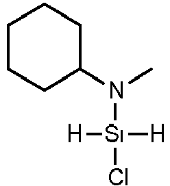


Cyclohexylmethylaminochlorosilane Cyclohexylethylaminochlorosilane Cyclohexyl-iso-propylaminochlorosilane 


Cyclohexylmethylaminodichlorosilane Cyclohexylethylaminodichlorosilane propylaminodichlorosilane 


Iso-propylmethylaminochlorosilane Iso-propylethylaminochlorosilane N-(chlorosilyl)perhydroquinoline 
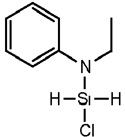

Phenylmethylaminochlorosilane Phenylethylaminochlorosilane Phenyl-iso-propylaminoclorosilane 


Phenylallylaminochlorosilane m-tolylmethylaminochlorosilane N-(chlorosilyl)-tetrahydroquinoline 


N-chlorosilyl-3-anilinopropionitrile N-chlorosilyl-N-phenylglycinonitrile N-(chlorosilyl)carbazole 


Phenylcyclohexylaminochlorosilane N-(chlorosilyl)-2-methylindoline N-(chlorosilyl)benzomorpholine 


N-(chlorosilyl)indole N-(chlorosilyl)-2-methylindole N-(chlorosilyl)-3-methylindole 


o-tolylethylaminochlorosilane p-tolylethylaminochlirosilane m-tolylethylaminochlorosilane 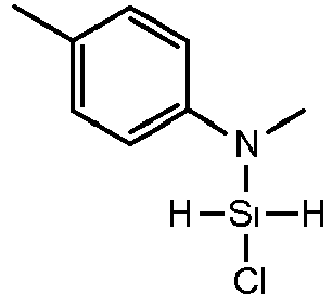


p-tolylmethylaminochlorosilane o-tolylmethylaminochlorosilane N-(chlorosilyl)-1,2,3,4-tetrahydro-2-methylquinoline - In certain embodiments, the halogenated organoaminosilane of Formula I comprises Cl as X and is selected from the group comprising: ClH2Si(NR2R3) wherein m=1, n=0, p=2, R2 is selected from a linear or branched C3 to C10 alkyl group and a C6 to C10 aryl group and R3 is a branched C3 to C10 alkyl group or a C6 to C10 aryl group and wherein R2 and R3 can form a cyclic or alkyl substituted cyclic ring; and R1ClHSi(NR3R4) wherein m=1, n= 1,p=1, R1 is a C1 to C10 alkyl group and R2 and R3 are a linear or branched C3 to C10 alkyl group or a C4 to C10 aryl group and wherein R2 and R3 can form a cyclic or a alkyl substituted cyclic ring.
- In certain embodiments, the halogenated organoaminosilanes having Formula I can be prepared by reacting 1 molar equivalent dichlorosilane (DCS) with 1 molar equivalent secondary amine or trichlorosilane (TCS) with 1 or 2 molar equivalent secondary amine having the following Formula II in an organic solvent or solvent mixture, using 1 or 2 molar equivalent tertiary amine such as triethylamine or tributylamine to absorb the byproduct, hydrogen chloride, preferably a tertiary amine is employed as demonstrated in Example 1 and 2 below). In certain embodiments, tertiary amines are replaced by equal molar of secondary amines. Selected secondary amines that can be used in this embodiment have following Formula II:

- Exemplary amines having Formula II wherein R2 and R3 are linked to form a ring include, but are not limited to, 2,6-dimethylpiperidine, 2-methylpiperidine, 2-methylpyrrolidine, 2,5-dimethylpyrrolidine, 2,2,6,6,-tetramethylpiperidine, 3-methylindole, 2-methylindole, indole, perhydoquinoline, 8-methyl-1,2,3,4-tetrahydroquinoline, 3-indoleacetonitrile, 2-methylindoline, 2,3-dihydroindole, 5-methylindoline, 1,2,3,4-tetrahydroquinoline, 1,2,3,4-tetrahydro-2-methylquinoline, 1,2,3,4-tetrahydro-6-methylquinoline, 3,4-dihydro-2H-1,4-benzoxazine, carbazole, 2,6-dimethylmorpholine and 3,5-dimethylmorpholine.
- The following Equations 1, 2 and 3 provide examples of reaction schemes or synthesis routes which may be used to make the halogenated organoaminosilanes having Formula I as described herein. The reactions in Equations 1, 2, and 3 can be conducted with (e.g. in the presence of) organic solvents. In embodiments wherein an organic solvent is used, examples of suitable organic solvents include, but are not limited to, hydrocarbon such as hexanes, octane, toluene, and ethers such as diethylether, and tetrahydrofuran (THF). In these or other embodiments, the reaction temperature is in the range of from about -70°C to the boiling point of the solvent employed if a solvent is involved. The resulting organoaminosilane can be purified via vacuum distillation after removing all by-products as well as solvent(s). Equation 1 - 3 are embodiments involving reaction of dichlorosilane or trichlorosilane. Examples of the synthetic route involving partial amination reaction are provided herein as Example 1 and 3 whereas Equation 2 involving metal amide which can be prepared via reaction of an amine with Formula II with metal alkyl is demonstrated in Example 2.

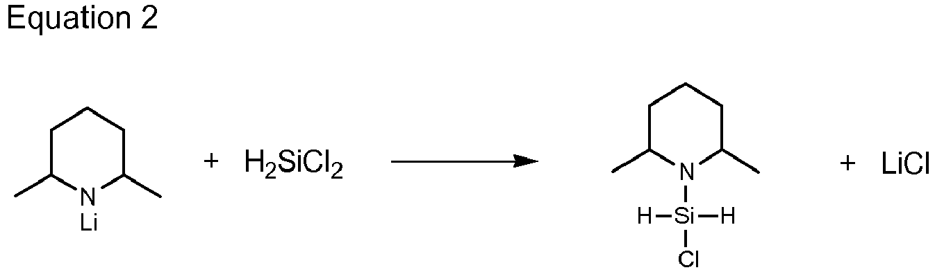

- The method used to form the silicon-containing dielectric films or coatings are deposition processes. Examples of suitable deposition processes for the method disclosed herein include, but are not limited to, cyclic CVD (CCVD), MOCVD (Metal Organic CVD), thermal chemical vapor deposition, plasma enhanced chemical vapor deposition ("PECVD"), high density PECVD, photon assisted CVD, plasma-photon assisted ("PPECVD"), cryogenic chemical vapor deposition, chemical assisted vapor deposition, hot-filament chemical vapor deposition, CVD of a liquid polymer precursor, deposition from supercritical fluids, and low energy CVD (LECVD). In certain embodiments, the metal containing films are deposited via atomic layer deposition (ALD), plasma enhanced ALD (PEALD) or plasma enhanced cyclic CVD (PECCVD) process. As used herein, the term "chemical vapor deposition processes" refers to any process wherein a substrate is exposed to one or more volatile precursors, which react and/or decompose on the substrate surface to produce the desired deposition. As used herein, the term "atomic layer deposition process" refers to a self-limiting (e.g., the amount of film material deposited in each reaction cycle is constant), sequential surface chemistry that deposits films of materials onto substrates of varying compositions. Although the precursors, reagents and sources used herein may be sometimes described as "gaseous", it is understood that the precursors can be either liquid or solid which are transported with or without an inert gas into the reactor via direct vaporization, bubbling or sublimation. In some case, the vaporized precursors can pass through a plasma generator. In one embodiment, the dielectric film is deposited using an ALD process. In another embodiment, the dielectric film is deposited using a CCVD process. In a further embodiment, the dielectric film is deposited using a thermal CVD process. The term "reactor" as used herein, includes without limitation, reaction chamber or deposition chamber.
- In certain embodiments, the method disclosed herein avoids pre-reaction of the precursors by using ALD or CCVD methods that separate the precursors prior to and/or during the introduction to the reactor. In this connection, deposition techniques such as ALD or CCVD processes are used to deposit the dielectric film. In one embodiment, the film is deposited via an ALD process by exposing the substrate surface alternatively to the one or more the silicon-containing precursor, oxygen source, nitrogen-containing source, or other precursor or reagent. Film growth proceeds by self-limiting control of surface reaction, the pulse length of each precursor or reagent, and the deposition temperature. However, once the surface of the substrate is saturated, the film growth ceases.
- In certain embodiments, the method described herein further comprises one or more additional silicon-containing precursors or non-halogenated other than the halogenated organoaminosilane precursor having the above Formula I. Examples of additional silicon-containing precursors include, but are not limited to, organo-silicon compounds such as siloxanes (e.g., hexamethyl disiloxane (HMDSO) and dimethyl siloxane (DMSO)); organosilanes (e.g., methylsilane; dimethylsilane; vinyl trimethylsilane; trimethylsilane; tetramethylsilane; ethylsilane; disilylmethane; 2,4-disilapentane; 1,4-disilabutane; 2,5-disilahexane; 2,2-disilylpropane; 1,3,5-trisilacyclohexane, and fluorinated derivatives of these compounds; phenyl-containing organo-silicon compounds (e.g., dimethylphenylsilane and diphenylmethylsilane); oxygen-containing organo-silicon compounds ,e.g., dimethyldimethoxysilane; 1,3,5,7-tetramethylcyclotetrasiloxane; 1,1,3,3-tetramethyldisiloxane; 1,3,5,7-tetrasila-4-oxo-heptane; 2,4,6,8-tetrasila-3,7-dioxo-nonane; 2,2-dimethyl-2,4,6,8-tetrasila-3,7-dioxononane; octamethylcyclotetrasiloxane; [1,3,5,7,9]-pentamethylcyclopentasiloxane; 1,3,5,7-tetrasila-2,6-dioxo-cyclooctane; hexamethylcyclotrisiloxane; 1,3-dimethyldisiloxane; 1,3,5,7,9-pentamethylcyclopentasiloxane; hexamethoxydisiloxane, and fluorinated derivatives of these compounds.
- In one particular embodiment of the method described herein, the non-halogenated, silicon-containing precursor is a compound having the following Formula III:
(R2R3N)SiH3 (III)
wherein R2 is selected from a linear or branched C1 to C10 alkyl, a C3 to C12 alkenyl group, a C3 to C12 alkynyl group, a C4 to C10 cyclic alkyl group, and a C6 to C10 aryl group; R3 is selected from a branched C3 to C10 alkyl group, a C3 to C12 alkenyl group, a C3 to C12 alkynyl group, a C4 to C10 cyclic alkyl group, and a C6 to C10 aryl group and wherein R2 and R3 are linked to form a ring or R2 and R3 are not linked to form a ring. In certain embodiments of Formula III, R2 and R3 can be combined to form a cyclic group or ring. In other embodiments of Formula III R2 and R3 are not combined to form a cyclic group or ring. Examples of non-halogenated silicon-containing precursors include, but are not limited to, di-iso-propylaminosilane, di-sec-butylaminosilane, phenylmethylaminosilane, and 2,6-dimethylpiperidinosilane. - Depending upon the deposition method, in certain embodiments, the one or more, halogenated or non-halogenated, silicon-containing precursors may be introduced into the reactor at a predetermined molar volume, or from about 0.1 to about 1000 micromoles. In this or other embodiments, the halogenated or non-halogenated organoaminosilane precursor may be introduced into the reactor for a predetermined time period. In certain embodiments, the time period ranges from about 0.001 to about 500 seconds.
- In certain embodiments, the dielectric films deposited using the methods described herein are formed in the presence of oxygen using an oxygen source, reagent or precursor comprising oxygen. An oxygen source may be introduced into the reactor in the form of at least one oxygen source and/or may be present incidentally in the other precursors used in the deposition process. Suitable oxygen source gases may include, for example, water (H2O) (e.g., deionized water, purifier water, and/or distilled water), oxygen (O2), oxygen plasma, ozone (O3), NO, NO2, carbon monoxide (CO), carbon dioxide (CO2) and combinations thereof. In certain embodiments, the oxygen source comprises an oxygen source gas that is introduced into the reactor at a flow rate ranging from about 1 to about 2000 standard cubic centimeters per minute (sccm) or from about 1 to about 1000 sccm. The oxygen source can be introduced for a time that ranges from about 0.1 to about 100 seconds. In one particular embodiment, the oxygen source comprises water having a temperature of 10°C or greater. In embodiments wherein the film is deposited by an ALD or a cyclic CVD process, the precursor pulse can have a pulse duration that is greater than 0.01 seconds, and the oxygen source can have a pulse duration that is less than 0.01 seconds, while the water pulse duration can have a pulse duration that is less than 0.01 seconds. In yet another embodiment, the purge duration between the pulses that can be as low as 0 seconds or is continuously pulsed without a purge in-between. The oxygen source or reagent is provided in a molecular amount less than a 1:1 ratio to the silicon precursor, so that at least some carbon is retained in the as deposited dielectric film.
- In certain embodiments, the dielectric films comprise silicon and nitrogen. In these embodiments, the dielectric films deposited using the methods described herein are formed in the presence of nitrogen-containing source. An nitrogen-containing source may be introduced into the reactor in the form of at least one nitrogen source and/or may be present incidentally in the other precursors used in the deposition process. Suitable nitrogen-containing source gases may include, for example, ammonia, hydrazine, monoalkylhydrazine, dialkylhydrazine, nitrogen, nitrogen/hydrogen, ammonia plasma, nitrogen plasma, nitrogen/hydrogen plasma, and mixture thereof. In certain embodiments, the nitrogen-containing source comprises an ammonia plasma or hydrogen/nitrogen plasma source gas that is introduced into the reactor at a flow rate ranging from about 1 to about 2000 standard cubic centimeters per minute (sccm) or from about 1 to about 1000 sccm. The nitrogen-containing source can be introduced for a time that ranges from about 0.1 to about 100 seconds. In embodiments wherein the film is deposited by an ALD or a cyclic CVD process, the precursor pulse can have a pulse duration that is greater than 0.01 seconds, and the nitrogen-containing source can have a pulse duration that is less than 0.01 seconds, while the water pulse duration can have a pulse duration that is less than 0.01 seconds. In yet another embodiment, the purge duration between the pulses that can be as low as 0 seconds or is continuously pulsed without a purge in-between.
- The deposition methods disclosed herein may involve one or more purge gases. The purge gas, which is used to purge away unconsumed reactants and/or reaction byproducts, is an inert gas that does not react with the precursors. Exemplary purge gases include, but are not limited to, argon (Ar), nitrogen (N2), helium (He), neon, hydrogen (H2), and mixtures thereof. In certain embodiments, a purge gas such as Ar is supplied into the reactor at a flow rate ranging from about 10 to about 2000 sccm for about 0.1 to 1000 seconds, thereby purging the unreacted material and any byproduct that may remain in the reactor.
- The respective step of supplying the precursors, oxygen source, the nitrogen-containing source, and/or other precursors, source gases, and/or reagents may be performed by changing the time for supplying them to change the stoichiometric composition of the resulting dielectric film.
- Energy is applied to the at least one of the precursor, nitrogen-containing source, reducing agent, other precursors or combination thereof to induce reaction and to form the dielectric film or coating on the substrate. Such energy can be provided by, but not limited to, thermal, plasma, pulsed plasma, helicon plasma, high density plasma, inductively coupled plasma, X-ray, e-beam, photon, remote plasma methods, and combinations thereof. In certain embodiments, a secondary RF frequency source can be used to modify the plasma characteristics at the substrate surface. In embodiments wherein the deposition involves plasma, the plasma-generated process may comprise a direct plasma-generated process in which plasma is directly generated in the reactor, or alternatively a remote plasma-generated process in which plasma is generated outside of the reactor and supplied into the reactor.
- The organoaminosilane precursors and/or other silicon-containing precursors may be delivered to the reaction chamber such as a CVD or ALD reactor in a variety of ways. In one embodiment, a liquid delivery system may be utilized. In an alternative embodiment, a combined liquid delivery and flash vaporization process unit may be employed, such as, for example, the turbo vaporizer manufactured by MSP Corporation of Shoreview, MN, to enable low volatility materials to be volumetrically delivered, which leads to reproducible transport and deposition without thermal decomposition of the precursor. In liquid delivery formulations, the precursors described herein may be delivered in neat liquid form, or alternatively, may be employed in solvent formulations or compositions comprising same. Thus, in certain embodiments the precursor formulations may include solvent component(s) of suitable character as may be desirable and advantageous in a given end use application to form a film on a substrate.
- For those embodiments wherein the halogenated organoaminosilane precursor(s) having Formula I is used in a composition comprising a solvent and an halogenated organoaminosilane precursor having Formula I described herein, the solvent or mixture thereof selected does not react with the organoaminosilane. The amount of solvent by weight percentage in the composition ranges from 0.5% by weight to 99.5% or from 10% by weight to 75%. In this or other embodiments, the solvent has a boiling point (b.p.) similar to the b.p. of the halogenated organoaminosilane of Formula I or the difference between the b.p. of the solvent and the b.p. of the halogenated organoaminosilane of Formula I is 40°C or less, 30°C or less, or 20°C or less, or 10°C. Alternatively, the difference between the boiling points ranges from any one or more of the following end-points: 0, 10, 20, 30, or 40°C. Examples of suitable ranges of b.p. difference include without limitation, 0 to 40°C, 20° to 30°C, or 10° to 30°C. Examples of suitable solvents in the compositions include, but are not limited to, an ether (such as 1,4-dioxane, dibutyl ether), a tertiary amine (such as pyridine, 1-methylpiperidine, 1-ethylpiperidine, N,N'-Dimethylpiperazine, N,N,N',N'-Tetramethylethylenediamine), a nitrile (such as benzonitrile), an alkyl hydrocarbon (such as octane, nonane, dodecane, ethylcyclohexane), an aromatic hydrocarbon (such as toluene, mesitylene), a tertiary aminoether (such as bis(2-dimethylaminoethyl) ether), or mixtures thereof. Some non-limiting exemplary compositions include, but not limited to, a composition comprising di-iso-propylaminosilane (b.p. about 116°C) and octane (b.p. 125 to 126°C); di-iso-propylaminosilane (b.p. about 116°C) and pyridine (b.p. 115°C); di-iso-propylaminosilane (b.p. about 116°C) and toluene (b.p. 110°C); a composition comprising N-methylcyclohexylaminosilane (b.p. about 171°C and decane (b.p. 174°C); a composition comprising N-methylcyclohexylaminosilane (b.p. about 171°C and diethylene glycol dimethyl ether (b.p. 162°C); a composition comprising N-iso-propylcyclohexylaminosilane (b.p. about 199°C) and bis(2-dimethylaminoethyl) ether (b.p., 189°C); N-iso-propylcyclohexylaminosilane (b.p. about 199°C) and benzonitrile (b.p., 191°C).
- In another embodiment, a vessel for depositing a dielectric film comprising one or more organoaminosilane precursor having Formula I is described herein. In one particular embodiment, the vessel comprises at least one pressurizable vessel (preferably of stainless steel) fitted with the proper valves and fittings to allow the delivery of one or more precursors to the reactor for a CVD or an ALD process. In this or other embodiments, the halogenated organoaminosilane precursor of Formula I is provided in a pressurizable vessel comprised of stainless steel and the purity of the precursor is 98% by weight or greater or 99.5% or greater which is suitable for the majority of semiconductor applications. In certain embodiments, such vessels can also have means for mixing the precursors with one or more additional precursor if desired. In these or other embodiments, the contents of the vessel(s) can be premixed with an additional precursor. Alternatively, the halogenated organoaminosilane precursor and/or other precursor can be maintained in separate vessels or in a single vessel having separation means for maintaining the organoaminosilane precursor and other precursor separate during storage. In certain embodiments, the halogenated organoaminosilane precursor having Formula I in the vessel further comprises a back fill gas(es) such as, but not limited to, nitrogen, an inert gas such as helium, or combinations thereof. In an alternative embodiment, the vessel does not contain a back fill gas.
- As previously mentioned, the purity level of the halogenated organoaminosilane is sufficiently high enough to be acceptable for reliable semiconductor manufacturing. In certain embodiments, the halogenated organoaminosilane precursors described herein comprise less than 2% by weight, or less than 1% by weight, or less than 0.5% by weight of one or more of the following impurities: free amines, free halides or an halogen ion, and higher molecular weight species. Higher purity levels of the organoaminosilanes described herein can be obtained through one or more of the following processes: purification, adsorption, and/or distillation.
- In one embodiment of the method described herein, a cyclic deposition process such as CCVD, ALD, or PEALD may be employed, wherein at least one silicon-containing precursor selected from a halogenated organoaminosilane precursor having Formula I and optionally a nitrogen-containing source such as, for example, ammonia, hydrazine, monoalkylhydrazine, dialkylhydrazine, nitrogen, nitrogen/hydrogen, ammonia plasma, nitrogen plasma, nitrogen/hydrogen plasma are employed.
- In certain embodiments, the gas lines connecting from the precursor canisters to the reaction chamber are heated to one or more temperatures depending upon the process requirements and the container of the halogenated organoaminosilane precursor having Formula I is kept at one or more temperatures for bubbling. In other embodiments, a solution comprising the at least one halogenated organoaminosilane precursor having Formula I is injected into a vaporizer kept at one or more temperatures for direct liquid injection.
- A flow of argon and/or other gas may be employed as a carrier gas to help deliver the vapor of the at least one organoaminosilane precursor to the reaction chamber during the precursor pulsing. In certain embodiments, the reaction chamber process pressure is about 1 Torr (130 Pa).
- In a typical ALD or CCVD process, the substrate such as a silicon oxide substrate is heated on a heater stage in a reaction chamber that is exposed to the silicon-containing precursor initially to allow the complex to chemically adsorb onto the surface of the substrate.
- A purge gas such as argon purges away unabsorbed excess complex from the process chamber. After sufficient purging, a nitrogen-containing source may be introduced into reaction chamber to react with the absorbed surface followed by another gas purge to remove reaction by-products from the chamber. The process cycle can be repeated to achieve the desired film thickness.
- In certain embodiments, the process employs a reducing agent. The reducing agent is typically introduced in gaseous form. Examples of suitable reducing agents include, but are not limited to, hydrogen gas, hydrogen plasma, remote hydrogen plasma, silanes (i.e., diethylsilane, ethylsilane, dimethylsilane, phenylsilane, silane, disilane, aminosilanes, chlorosilanes), boranes (i.e., borane, diborane), alanes, germanes, hydrazines, ammonia, or mixtures thereof. In one particular embodiment such as the deposition of amorphous silicon, a reducing agent is used.
- In this or other embodiments, it is understood that the steps of the methods described herein may be performed in a variety of orders, may be performed sequentially or concurrently (e.g., during at least a portion of another step), and any combination thereof. The respective step of supplying the precursors and the nitrogen-containing source gases may be performed by varying the duration of the time for supplying them to change the stoichiometric composition of the resulting dielectric film.
- In another embodiment of the method disclosed herein, the films containing both silicon and nitrogen are formed using a ALD deposition method that comprises the steps of:
- providing a substrate in an ALD reactor;
- introducing into the ALD reactor an at least one halogenated organoaminosilane precursor represented by the following Formula I:
XmR1 nHpSi(NR2R3)4-m-n-p I
wherein X is a halide selected from the group consisting of Cl, Br, I; R1 is independently selected from a linear or branched C1 to C10 alkyl group, a C2 to C12 alkenyl group, a C2 to C12 alkynyl group, a C4 to C10 cyclic alkyl, and a C6 to C10 aryl group; R2 is selected from a linear or branched C1 to C10 alkyl, a C3 to C12 alkenyl group, a C3 to C12 alkynyl group, a C4 to C10 cyclic alkyl group, and a C6 to C10 aryl group; R3 is selected from a branched C3 to C10 alkyl group, a C3 to C12 alkenyl group, a C3 to C12 alkynyl group, a C4 to C10 cyclic alkyl group, and a C6 to C10 aryl group; m is 1 or 2; n is 0, 1, or 2; p is 0, 1 or 2; and the sum of (m+n+p) is less than 4 and wherein R2 and R3 are linked to form a ring or R2 and R3 are not linked to form a ring; - chemisorbing the at least one halogenated organoaminosilane precursor onto a substrate;
- purging away the unreacted at least one organoaminosilane precursor using a purge gas;
- providing a nitrogen-containing source to the organoaminosilane precursor onto the heated substrate to react with the sorbed at least one organoaminosilane precursor; and
- optionally purging away any unreacted nitrogen-containing source.
- In another embodiment of the method disclosed herein, the dielectric films is formed using a ALD deposition method that comprises the steps of:
- providing a substrate in a reactor;
- introducing into the reactor an at least one halogenated organoaminosilane precursor represented by the following Formula I:
XmR1 nHpSi(NR2R3)4-m-n-p I
wherein X is a halide selected from the group consisting of Cl, Br, I; R1 is independently selected from a linear or branched C1 to C10 alkyl group, a C2 to C12 alkenyl group, a C2 to C12 alkynyl group, a C4 to C10 cyclic alkyl, and a C6 to C10 aryl group; R2 is selected from a linear or branched C1 to C10 alkyl, a C3 to C12 alkenyl group, a C3 to C12 alkynyl group, a C4 to C10 cyclic alkyl group, and a C6 to C10 aryl group; R3 is selected from a branched C3 to C10 alkyl group, a C3 to C12 alkenyl group, a C3 to C12 alkynyl group, a C4 to C10 cyclic alkyl group, and a C6 to C10 aryl group; m is 1 or 2; n is 0, 1, or 2; p is 0, 1 or 2; and the sum of (m+n+p) is less than 4 and wherein R2 and R3 are linked to form a ring or R2 and R3 are not linked to form a ring; - chemisorbing the at least one organoaminosilane precursor onto a substrate;
- purging away the unreacted at least one organoaminosilane precursor using a purge gas;
- providing an oxygen source to the organoaminosilane precursor onto the heated substrate to react with the sorbed at least one organoaminosilane precursor; and
- optionally purging away any unreacted oxygen source.
- The above steps define one cycle for the method described herein; and the cycle can be repeated until the desired thickness of a dielectric film is obtained. In this or other embodiments, it is understood that the steps of the methods described herein may be performed in a variety of orders, may be performed sequentially or concurrently (e.g., during at least a portion of another step), and any combination thereof. The respective step of supplying the precursors and oxygen source may be performed by varying the duration of the time for supplying them to change the stoichiometric composition of the resulting dielectric film, although always using oxygen in less than a stoichiometric amount relative to the available silicon.
- For multi-component dielectric films, other precursors such as silicon-containing precursors, nitrogen-containing precursors, reducing agents, or other reagents can be alternately introduced into the reactor chamber.
- In a further embodiment of the method described herein, the dielectric film is deposited using a thermal CVD process. In this embodiment, the method comprises:
- placing one or more substrates into a reactor which is heated to a temperature ranging from ambient temperature to about 700°C and maintained at a pressure of 1 Torr (130 Pa) or less;
- introducing at least one halogenated organoaminosilane precursor having the following Formula I:
XmR1 nHpSi(NR2R3)4-m-n-p I
wherein X is a halide selected from the group consisting of Cl, Br, I; R1 is independently selected from a linear or branched C1 to C10 alkyl group, a C2 to C12 alkenyl group, a C2 to C12 alkynyl group, a C4 to C10 cyclic alkyl, and a C6 to C10 aryl group; R2 is selected from a linear or branched C1 to C10 alkyl, a C3 to C12 alkenyl group, a C3 to C12 alkynyl group, a C4 to C10 cyclic alkyl group, and a C6 to C10 aryl group; R3 is selected from a branched C3 to C10 alkyl group, a C3 to C12 alkenyl group, a C3 to C12 alkynyl group, a C4 to C10 cyclic alkyl group, and a C6 to C10 aryl group; m is 1 or 2; n is 0, 1, or 2; p is 0, 1 or 2; and the sum of (m+n+p) is less than 4 and wherein R2 and R3 are linked to form a ring or R2 and R3 are not linked to form a ring; and - providing an oxygen source into the reactor to at least partially react with the at least one organoaminosilane precursor and deposit a dielectric film onto the one or more substrates. In certain embodiments of the CVD method, the reactor is maintained at a pressure ranging from 100 mTorr to 600 mTorr (13 to 80 Pa) during the introducing step.
- The above steps define one cycle for the method described herein; and the cycle can be repeated until the desired thickness of a dielectric film is obtained. In this or other embodiments, it is understood that the steps of the methods described herein may be performed in a variety of orders, may be performed sequentially or concurrently (e.g., during at least a portion of another step), and any combination thereof. The respective step of supplying the precursors and oxygen source may be performed by varying the duration of the time for supplying them to change the stoichiometric composition of the resulting dielectric film, although always using oxygen in less than a stoichiometric amount relative to the available silicon.
- For multi-component dielectric films, other precursors such as silicon-containing precursors, nitrogen-containing precursors, oxygen sources, reducing agents, and/or other reagents can be alternately introduced into the reactor chamber.
- In a further embodiment of the method described herein, the dielectric film is deposited using a thermal CVD process. In this embodiment, the method comprises:
- placing one or more substrates into a reactor which is heated to a temperature ranging from ambient temperature to about 700°C and maintained at a pressure of 1 Torr (130 Pa) or less;
- introducing at least one halogenated organoaminosilane precursor having the following Formula I:
XmR1 nHpSi(NR2R3)4-m-n-p I
wherein X is a halide selected from the group consisting of Cl, Br, I; R1 is independently selected from a linear or branched C1 to C10 alkyl group, a C2 to C12 alkenyl group, a C2 to C12 alkynyl group, a C4 to C10 cyclic alkyl group, and a C6 to C10 aryl group; R2 is selected from a linear or branched C3 to C10 alkyl group, a C3 to C12 alkenyl group, a C3 to C12 alkynyl group, a C4 to C10 cyclic alkyl group, and a C6 to C10 aryl group; R3 is selected from a branched C3 to C10 alkyl group, a C3 to C12 alkenyl group, a C3 to C12 alkynyl group, a C4 to C10 cyclic alkyl group, and a C6 to C10 aryl group; m is 1 or 2; n is 0, 1, or 2; p is 0, 1 or 2; and the sum of (m+n+p) is less than 4 and wherein R2 and R3 are linked to form a ring or R2 and R3 are not linked to form a ring; and - providing a nitrogen-containing source into the reactor to at least partially react with the at least one organoaminosilane precursor and deposit a dielectric film onto the one or more substrates. In certain embodiments of the CVD method, the reactor is maintained at a pressure ranging from 100 mTorr to 600 mTorr (13 to 80 Pa) during the introducing step.
- As previously mentioned, the process described herein can be used to deposit a film using more than one precursor such as the halogenated organoaminosilane having Formula I described herein with an additional precursor such as a non-halogenated organoaminosilane precursor having Formula III described herein, a silicon-containing precursor such as those described herein, and/or a chlorosilane (such as, but not limited to, monochlorosilane (MCS), diclorosilane (DCS), trichlorosilane or tetrachlorosilane), and/or alkylchlorosilane (such as, but not limited to, methylchlorosilane, ethylchlorosilane, methyldichlorosilane, ethyldichlorosilane). In these embodiments, the one or more precursors are described as a first precursor, a second precursor, a third precursor, etc. depending upon the number of different precursors used. The process can be used, for example, in a cyclic chemical vapor deposition or an atomic layer deposition. In these or other embodiments, the precursors can be introduced in a variety of ways (e.g., a) introduce first precursor; b) purge; c) introduce second precursor; d) purge; e) introduce third precursor; f) purge, etc., or, alternatively, a) introduce first precursor; b) purge; c) introduce second precursor; d) purge; e) introduce second precursor; etc.) In one particular embodiment, there is provided a process to deposit silicon oxide film or a silicon, carbon, and oxide film comprising the following steps:
- a). Contacting vapors generated from a first precursor with a heated substrate to chemically sorb the first precursor on the heated substrate;
- b). Purging away any unsorbed precursors;
- c). Introducing an oxygen source on the heated substrate to react with the sorbed first precursor;
- d). Purging away any unreacted oxygen source;
- e). Contacting vapors generated from a second precursor which is different from the first precursor with a heated substrate to chemically sorb the second precursor on the heated substrate;
- f). Purging away any unsorbed precursors;
- g). Introducing an oxygen source on the heated substrate to react with the sorbed first and second precursors; and
- h). Purging away any unreacted oxygen source
- In a yet another embodiment of the process described herein, there is provided a method of depositing a silicon nitride or silicon carbonitride film comprising the following steps:
- a). Contacting vapors generated from a first precursor with a heated substrate to chemically sorb the first precursors on the heated substrate;
- b). Purging away any unsorbed first precursors;
- c). Introducing a nitrogen source on the heated substrate to react with the sorbed first precursor;
- d). Purging away any unreacted nitrogen source;
- e). Contacting vapors generated from a second precursor which is different from the first with a heated substrate to chemically sorb the second precursor on the heated substrate;
- f). Purging away any unsorbed second precursors;
- g). Introducing a nitrogen source on the heated substrate to react with the sorbed second precursor; and
- h). Purging away any unreacted nitrogen source
- In a further embodiment, described herein is a process is deposit silicon-containing films employing cyclic chemical vapor deposition (CCVD) or atomic layer deposition (ALD) techniques such as, but not limited to, plasma enhanced ALD (PEALD) or plasma enhanced CCVD (PECCVD) process. In these embodiments, the deposition temperature may be relatively high, or from about 500 to 800°C, to control the specifications of film properties required in certain semiconductor applications. In one particular embodiment, the process comprises the following steps: contacting vapors generated from a halogenated organoaminosilane having Formula I with a heated substrate to chemically sorb the precursors on the heated substrate; purging away any unsorbed precursors; introducing a reducing agent to reduce the sorbed precursors; and purging away any unreacted reducing agent.
- In certain embodiments, the halogenated organoaminosilane precursors having Formula I described herein can also be used a dopant for metal containing films, such as but not limited to, metal oxide films or metal nitride films. In these embodiments, the metal containing film is deposited using an ALD or CVD process such as those processes described herein using metal alkoxide, metal amide, or volatile organometallic precursors. Examples of suitable metal alkoxide precursors that may be used with the method disclosed herein include, but are not limited to, group 3 to 6 metal alkoxide, group 3 to 6 metal complexes having both alkoxy and alkyl substituted cyclopentadienyl ligands, group 3 to 6 metal complexes having both alkoxy and alkyl substituted pyrrolyl ligands, group 3 to 6 metal complexes having both alkoxy and diketonate ligands; group 3 to 6 metal complexes having both alkoxy and ketoester ligands; Examples of suitable metal amide precursors that may be used with the method disclosed herein include, but are not limited to, tetrakis(dimethylamino)zirconium (TDMAZ), tetrakis(diethylamino)zirconium (TDEAZ), tetrakis(ethylmethylamino)zirconium (TEMAZ), tetrakis(dimethylamino)hafnium (TDMAH), tetrakis(diethylamino)hafnium (TDEAH), and tetrakis(ethylmethylamino)hafnium (TEMAH), tetrakis(dimethylamino)titanium (TDMAT), tetrakis(diethylamino)titanium (TDEAT), tetrakis(ethylmethylamino)titanium (TEMAT), tert-butylimino tri(diethylamino)tantalum (TBTDET), tert-butylimino tri(dimethylamino)tantalum (TBTDMT), tert-butylimino tri(ethylmethylamino)tantalum (TBTEMT), ethylimino tri(diethylamino)tantalum (EITDET), ethylimino tri(dimethylamino)tantalum (EITDMT), ethylimino tri(ethylmethylamino)tantalum (EITEMT), tert-amylimino tri(dimethylamino)tantalum (TAIMAT), tert-amylimino tri(diethylamino)tantalum, pentakis(dimethylamino)tantalum, tert-amylimino tri(ethylmethylamino)tantalum, bis(tert-butylimino)bis(dimethylamino)tungsten (BTBMW), bis(tert-butylimino)bis(diethylamino)tungsten, bis(tert-butylimino)bis(ethylmethylamino)tungsten, and combinations thereof. Examples of suitable organometallic precursors that may be used with the method disclosed herein include, but are not limited to, group 3 metal cyclopentadienyls or alkyl cyclopentadienyls. Exemplary Group 3 to 6 metal herein include, but not limited to, Y, La, Ce, Pr, Nd, Sm, Eu, Gd, Tb, Dy, Er, Yb, Lu, Ti, Hf, Zr, V, Nb, Ta, Cr, Mo, and W. Other volatile organometallic precursors include, but are not limited to, metal alkyl precursors such as without limitation triethylaluminum (TEA), trimethylaluminum (TMA).
- In certain embodiments, the halogenated organoaminosilanes can be used in a liquid-based deposition or film formation method such as, but not limited to, spin-on, dip coat, aerosol, ink jet, screen printing or spray applications. In embodiments where the silicon film is formed through a liquid-based deposition, the composite film is formed from a composition that comprises, inter alia, at least one silicon-containing precursor such as the halogenated organoaminosilane having Formula I described herein as a silica source, a catalyst, and water. The composition may further comprise a solvent and a surfactant. In brief, dispensing the composition onto a substrate and evaporating the solvent and water can form the film. The surfactant, remaining solvent and water are generally removed by exposing the coated substrate to one or more energy sources and for a time sufficient to produce the silicon-containing film. In some instances, the film may be pre-heated to substantially complete the hydrolysis of the silica source, continue the crosslinking process, and drive off any remaining solvent, if present, from the film.
- Besides the halogenated organoaminosilane having Formula I described herein, another example of a silica source may include compounds that produce a Si-H bond upon removal of the pore-forming material.
- Still further examples of the source are found in the non-hydrolytic chemistry methods described, for example, in the references Hay et al., "Synthesis of Organic-Inorganic Hybrids via the Non-hydrolytic Sol-Gel Process", Chem. Mater., 13, 3396-3403 (2001) or Hay, et al., "A Versatile Route to Organically-Modified Silicas and Porous Silicas via the Non-Hydrolytic Sol-Gel Process", J. Mater. Chem., 10, 1811-1818 (2000).
- Yet another example of the silica source may include colloidal silica, fumed silica, or silicic acid starting materials.
- Still other examples of silica sources include silsesquioxanes such as hydrogen silsesquioxanes (HSQ, HSiO1.5) and methyl silsesquioxanes (MSQ, RSiO1.5 where R is a methyl group).
- In certain embodiments, the silica source may be added to the mixture as the product of hydrolysis and condensation. Hydrolysis and condensation of the silica source occurs by adding water and a catalyst to a solvent and adding the silica source at a time, intermittently or continuously, and conducting hydrolysis and condensation reactions while stirring the mixture at a temperature range generally from -30 to 100°C, preferably from 20 to 100°C, for 0 to 24 hours. The composition can be regulated to provide a desired solid content by conducting concentration or dilution with the solvent in each step of the preparation. Further, the silica source may be a compound that generates acetic acid when hydrolyzed.
- The hydrolysis and condensation of the silica source can occur at any point during the formation of the film, i.e., before adding to the mixture, after adding to the mixture, prior to, and/or during exposure to at least one energy source, etc. For example, in certain embodiments, the at least one silica source is combined with the solvent, water, and surfactant in a vessel and the catalyst is gradually added into the vessel and mixed. It is envisioned that a variety of different orders of addition to the mixture can be used without departing from the spirit of the present invention.
- The catalyst suitable for the present invention includes any organic or inorganic acid or base that can catalyze the hydrolysis of substitutents from the silica source in the presence of water, and/or the condensation of two silica sources to form a Si-O-Si bridge. The catalyst can be an organic base such as, but not limited to, quaternary ammonium salts and hydroxides, such as ammonium or tetramethylammonium, amines such as primary, secondary, and tertiary amines, and amine oxides. The catalyst can also be an acid such as, but not limited to, nitric acid, maleic, oxalic, acetic, formic, glycolic, glyoxalic acid, or mixtures thereof. In preferred embodiments, the catalyst comprises nitric acid.
- Solvents that are suitable for the use in the present invention may include any solvents that exhibit solubility with the reagents. Solvents can be, for example, alcohol solvents, ketone solvents, amide solvents, or ester solvents. In certain embodiments the solvents may be a supercritical fluid such as carbon dioxide, fluorocarbons, sulfur hexafluoride, alkanes, and other suitable multi-component mixtures, etc. In certain embodiments, one or more solvents used in the present invention have relatively low boiling points, i.e., below 160°C. These solvents include, but are not limited to, tetrahydrofuran, acetone, 1,4-dioxane, 1,3-dioxolane, ethyl acetate, and methyl ethyl ketone. Other solvents, that can be used in the present invention but have boiling points above 160°C, include dimethylformamide, dimethylacetamide, N-methyl pyrrolidone, ethylene carbonate, propylene carbonate, glycerol and derivatives, naphthalene and substituted versions, acetic acid anyhydride, propionic acid and propionic acid anhydride, dimethyl sulfone, benzophenone, diphenyl sulfone, phenol, m-cresol, dimethyl sulfoxide, diphenyl ether, terphenyl, and the like. Preferred solvents include propylene glycol propyl ether (PGPE), 3-heptanol, 2-methyl-1-pentanol, 5-methyl-2-hexanol, 3-hexanol, 2-heptano, 2-hexanol, 2,3-dimethyl-3-pentanol, propylene glycol methyl ether acetate (PGMEA), ethylene glycol n-butyl ether, propylene glycol n-butyl ether (PGBE), 1-butoxy-2-propanol, 2-methyl-3-pentanol, 2-methoxyethyl acetate, 2-butoxyethanol, 2-ethoxyethyl acetoacetate, 1-pentanol, and propylene glycol methyl ether. Still further exemplary solvents include lactates, pyruvates, and diols. Further exemplary solvents include those solvents listed in
EP 1,127,929 . The solvents enumerated above may be used alone or in combination of two or more solvents. - In certain embodiments, the reagents within the composition react to form a condensed flowable film on the substrate. This film flows into the gap to fill the gap with the dielectric material. The film is then converted to a solid dielectric material by one or more of various techniques including a thermal anneal, ultraviolet (UV) exposure, microwave exposure, or exposure to an oxidizing plasma. According to certain embodiments, the film is converted to the solid material by mechanisms including (but not limited to) cross-linking the precursor to produce the solid material and/or removal of hydrogen (--H), hydroxyl (--OH) or water (H2O) groups. In a particular embodiment, an inductively-coupled plasma is used to convert the film.
- In certain embodiments, the resultant dielectric films or coatings can be exposed to a post-deposition treatment such as, but not limited to, a plasma treatment, chemical treatment, ultraviolet light exposure, electron beam exposure, and/or other treatments to affect one or more properties of the film.
- In certain embodiments, the dielectric films described herein have a dielectric constant of 6 or less. In these or other embodiments, the films can a dielectric constant of about 5 or below, or about 4 or below, or about 3.5 or below. However, it is envisioned that films having other dielectric constants (e.g., higher or lower) can be formed depending upon the desired end-use of the film. In one embodiment of the silicon containing or dielectric film that is formed using the organoaminosilane precursors and processes described herein has the formulation SixOyCzNvHw wherein Si ranges from about 10% to about 40%; O ranges from about 0% to about 65%; C ranges from about 0% to about 75% or from about 0% to about 50%; N ranges from about 0% to about 75% or from about 0% to 50%; and H ranges from about 0% to about 50% atomic percent weight % wherein x+y+z+v+w = 100 atomic weight percent, as determined for example, by XPS or other means. However, other embodiments of dielectric or silicon-containg films with different formulations can be made using the halogenated organoaminosilane precursors described herein.
- As mentioned previously, the method described herein may be used to deposit a silicon-containing film on at least a portion of a substrate. Examples of suitable substrates include but are not limited to, silicon, SiO2, Si3N4, OSG, FSG, silicon carbide, hydrogenated silicon carbide, silicon nitride, hydrogenated silicon nitride, silicon carbonitride, hydrogenated silicon carbonitride, boronitride, antireflective coatings, photoresists, organic polymers, porous organic and inorganic materials, metals such as copper and aluminum, and diffusion barrier layers such as but not limited to TiN, Ti(C)N, TaN, Ta(C)N, Ta, W, or WN. The films are compatible with a variety of subsequent processing steps such as, for example, chemical mechanical planarization (CMP) and anisotropic etching processes.
- The deposited films have applications, which include, but are not limited to, computer chips, optical devices, magnetic information storages, coatings on a supporting material or substrate, microelectromechanical systems (MEMS), nanoelectromechanical systems, thin film transistor (TFT), and liquid crystal displays (LCD).
- In the claims, letters are used to identify claimed steps (e.g. (a), (b), and (c)). These letters are used to aid in referring to the method steps and are not intended to indicate the order in which claimed steps are performed, unless and only to the extent that such order is specifically recited in the claims.
- The following examples illustrate the method for preparing halogenated organoaminosilane precursors described herein as well as deposited silicon-containing films described herein and are not intended to limit it in any way.
- In a 2000 ml 3-necked round bottom flask equipped with mechanical stirror and an addition funnel, 1000 ml hexane was added. With the flask was cooled to -20 °C using a dry ice IPA cold bath, 101 g (1.0 mol) dichlorosilane was condensed and dissolved into hexane. With stirring, a mixture of 113 g (1.0 mol) 2,6-dimethylpiperidine and 111 g (1.1 mol) triethylamine was added dropwise to the flask. After the addition was complete, the reaction mixture was stirred at -20 °C for 1 hour, and then let warming up to room temperature. A salt byproduct precipitate of HCl•Et3N was removed by vacuum filtration in a glove bag purging with N2 to prevent the product reacting with the moisture in the air. A GC/MS analysis on the filtrate confirmed the product 2,6-dimethylpiperidinochlorosilane, showing the product with a molecular ion mass of 177 and supporting mass fragment of mass M -CH3 of 162. The solvent hexane was removed by distillation and the product was separated by vacuum distillation. The boiling point was 60°C at 10 torr (1300 Pa). The yield was 66%.
- To a solution of 7.55g (66.68mmol) cis-2,6-dimethylpiperidine in 50mL of THF at -78°C was drop-wise added 28.00mL (70.02mmol) of a 2.5M solution of n-butyllithium in hexanes. A precipitate evolved and the reaction mixture was warmed to room temperature while stirring. After one hour this mixture was added drop-wise to a solution of 6.74g (66.68mmol) dichlorosilane in 30mL xylenes and 70mL hexanes at -40°C and a light gray precipitate formed. The reaction mixture was stirred for 16 hours after which it was decanted from the evolved solid and subjected to distillation at ambient pressure to remove volatiles. 3.16g of desired product was isolated with a yield of 27%. The product was confirmed by GC/MS analysis as 2,6-Dimethylpiperidinochlorosilane.
- A synthesis of 2,6-dimethylpiperidinodichlorosilane was produced by mixing a mole ratio of 1 part 2,6-dimethylpiperdine to 1 part triethylamine to 1.1 part trichlorosilane in a 70% by weight hexane solution. An excess amount of trichlorosilane was needed to prevent the formation of bis(2,6-dimethylpiperindo)chlorosilane. A salt byproduct precipitate of HCl•Et3N was removed by vacuum filtration in a glove bag purging with N2 to prevent the product reacting with the moisture in the air. A GC/MS analysis (which is shown in
Figure 1 ) on the filtrate confirmed the product 2,6-dimethylpiperidinodichlorosilane was produced, resulting a mass of 211 and supporting mass fragment of mass -CH3 of 196. After vacuum filtration, the gross amount of hexane was removed be by simple distillation in the first step. The second step used the vacuum distillation technique, which the procuct was collected. A boiling points were determined from the vacuum distillation is 93°C at 18 torr (2400 Pa), and 66°C at 5 torr (670 Pa). The yield was 64%. - Atomic layer depositions of silicon-containing films were conducted using the following precursor: 2,6-dimethylpiperidinochlorosilane. The depositions were performed on a laboratory scale ALD processing tool. All gases (e.g., purge and reactant gas or precursor and oxygen source) were preheated to 100°C prior to entering the deposition zone. Gases and precursor flow rates were controlled with ALD diaphragm valves having high speed actuation. The substrates used in the deposition were 12 inch (30 cm) length silicon strips having thermocouple attached on a sample holder to confirm the substrate temperature. Depositions were performed using ozone as the oxygen source gas and the process parameters of the depositions are provided in Table II:
Table II: Process for Atomic Layer Deposition of Silicon-containing Films with Ozone Step a) 6sec Chamber evacuation <100mT (13 Pa) Prepare the reactor for the precursor dose Step b) Variable Dose halogenated organoaminosilane Precursor Reactor pressure typically <1Torr (130 Pa) during dose Step c) 6sec Nitrogen purge of reactor Flow 1.5 Slpm (standard litres per minute) N2 Purges out unreacted chemical from reactor Step d) 6sec Chamber evacuation <100mT (13 Pa) Prepare the reactor for the organoaminosilane precursor dose Step e) 2sec Dose Ozone ozone at 18-20%wt post generator, P=<8Torr (1100 Pa) - Steps b) to e) are repeated until a desired thickness is reached. The resultant silicon-containing films were characterized for deposition rate and refractive index. Thickness and refractive indices of the films was measured using a FilmTek 2000SE ellipsometer by fitting the reflection data from the film to a pre-set physical model (e.g., the Lorentz Oscillator model). Film composition was analyzed with X-Ray Photoelectron Spectroscopy (XPS) technique. The X-ray Photoelectron Spectroscopy experiments are performed on a PHI 5000VersaProbe Spectrometer equipped with Multiple Channels Plates (MCD) and a focused Al monochromatic X-ray source. Film compositions were measured at 100Å into the film to remove adventitious carbon signal. The measured film composition omitted hydrogen, as it is not detectable with XPS, and normalized to 100%.
- X-ray Reflectometry (XRR) was performed on all samples to determine film density. Samples were scanned over the range 0.2 ≤ 2 ≤ 0.65 0.65 using a step size of 0.001 and a count time of 1s/step. Data were analyzed using a two-layer model with the substrate defined as Si and film as silicon oxide.
- Silicon oxide films were formed using 2,6-dimethylpiperidinochlorosilane at various substrate temperature from 150 to 300°C at one second precursor dose as summarized in Table III:
TABLE III. Summary of Process Parameters and Results for 2,6-dimethylpiperidinochlorosilane No. Wafer temperature (Celsius) Precursor dose (seconds) Deposition Rate (Å/cycle) 1 50 1 0.15 2 150 1 0.22 3 300 1 0.55 - Silicon oxide films were formed using 2,6-dimethylpiperidinochlorosilane at substrate temperature of 300°C at variable precursor doses as summarized in Table IV:
Table IV: Summary of Process Parameters and Results for 2,6-dimethylpiperidinochlorosilane No. Wafer temperature (Celsius) Precursor dose (seconds) Deposition Rate (Å/cycle) Refractive index 1 300 0.5 0.43 1.46 2 300 1 0.55 1.49 3 300 2 0.60 1.48 4 300 4 0.50 1.51 - Silicon oxide deposition shows deposition rate saturation with increasing precursor dose, demonstrating a self-limited atomic layer deposition (ALD) like behavior. Deposited films have 33 at.% of Si and 67 at.% O, as measured by X-ray photospectroscopy (XPS). No carbon, nitrogen and chlorine were detected in the films. Film density is 1.9 ± 0.05 g/cc.
- Further preferred aspects of the invention include:
- #1. A halogenated organoaminosilane precursor represented by the following Formula I:
XmR1 nHpSi(NR2R3)4-m-n-p I
wherein X is a halide selected from the group consisting of Cl, Br, I; R1 is independently selected from a linear or branched C1 to C10 alkyl group, a C2 to C12 alkenyl group, a C2 to C12 alkynyl group, a C4 to C10 cyclic alkyl group, and a C6 to C10 aryl group; R2 is selected from a linear or branched C1 to C10 alkyl, a C3 to C12 alkenyl group, a C3 to C12 alkynyl group, a C4 to C10 cyclic alkyl group, and a C6 to C10 aryl group; R3 is selected from a branched C3 to C10 alkyl group, a C3 to C12 alkenyl group, a C3 to C12 alkynyl group, a C4 to C10 cyclic alkyl group, and a C6 to C10 aryl group; m is 1 or 2; n is 0, 1, or 2; p is 0, 1 or 2; and the sum of (m+n+p) is less than 4 and wherein R2 and R3 are linked to form a ring. - #2. The halogenated organoaminosilane precursor of #1 wherein R1 and R2 are the same.
- #3. The halogenated organoaminosilane precursor of #1 wherein R1 and R2 are different.
- #4. A method for forming a dielectric film on at least one surface of a substrate by a deposition process chosen from a chemical vapor deposition process and an atomic layer deposition process, the method comprising:
- providing the at least one surface of the substrate in a reaction chamber;
- introducing at least one halogenated organoaminosilane precursor having the following Formula I:
XmR1 nHpSi(NR2R3)4-m-n-p I
introducing a nitrogen-containing source into the reactor wherein the at least one organoaminosilane precursor and the nitrogen-containing source react to the dielectric films on the at least one surface. - #5. The method of #4 wherein the at least one organoaminosilane precursor is selected from the group consisting of 2,6-dimethylpiperidinodichlorosilane, 2,6-dimethylpiperidinochlorosilane, cyclohexylmethylaminochlorosilane, cyclohexylethylaminochlorosilane, and cyclohexyl-iso-propylaminochlorosilane.
- #6. The method of #5 wherein the at least one organoaminosilane precursor comprises 2,6-dimethylpiperidinodichlorosilane.
- #7. The method of #5 wherein the at least one organoaminosilane precursor comprises 2,6-dimethylpiperidinochlorosilane.
- #8. The method of #4 wherein the nitrogen-containing source is selected from the group consisting of ammonia, hydrazine, monoalkylhydrazine, dialkylhydrazine, nitrogen/hydrogen, ammonia plasma, nitrogen plasma, nitrogen/hydrogen plasma, and mixtures thereof.
- #9. The method of #4 wherein the dielectric film is selected from the group consisting of silicon nitride and silicon carbonitride.
- #10. A method of forming a dielectric film via an atomic layer deposition (ALD) process, the method comprising the steps of:
- a. providing a substrate in an ALD reactor;
- b. providing in the ALD reactor an at least one halogenated organoaminosilane precursor having the following Formula I:
XmR1 nHpSi(NR2R3)4-m-n-p I
wherein X is a halide selected from the group consisting of Cl, Br, I; R1 is independently selected from a linear or branched C1 to C10 alkyl group, a C2 to C12 alkenyl group, a C2 to C12 alkynyl group, a C4 to C10 cyclic alkyl, and a C6 to C10 aryl group; R2 is selected from a linear or branched C3 to C10 alkyl group, a C3 to C12 alkenyl group, a C3 to C12 alkynyl group, a C4 to C10 cyclic alkyl group, and a C6 to C10 aryl group; R3 is selected from a branched C1 to C10 alkyl, a C3 to C12 alkenyl group, a C3 to C12 alkynyl group, a C4 to C10 cyclic alkyl group, and a C6 to C10 aryl group; m is 1 or 2; n is 0, 1, or 2; p is 0, 1 or 2; and the sum of (m+n+p) is less than 4 and wherein R2 and R3 are linked to form a ring or R2 and R3 are not linked to form a ring; - c. purging the ALD reactor with an inert gas;
- d. providing a nitrogen-containing source in the ALD reactor;
- e. purging the ALD reactor with an inert gas; and
repeating the steps b through e until a desired thickness of the dielectric film is obtained.
- #11. The method of #10 wherein the at least one halogenated organoaminosilane precursor is selected from the group consisting of 2,6-dimethylpiperidinodichlorosilane, 2,6-dimethylpiperidinochlorosilane, cyclohexylmethylaminochlorosilane, cyclohexylethylaminochlorosilane, and cyclohexyl-iso-propylaminochlorosilane.
- #12. The method of #11 wherein the at least one halogenated organoaminosilane precursor comprises 2,6-dimethylpiperidinodichlorosilane.
- #13. The method of #11 wherein the at least one halogenated organoaminosilane precursor comprises 2,6-dimethylpiperidinochlorosilane.
- #14. The method of #10 wherein the nitrogen-containing source is selected from the group consisting of ammonia, hydrazine, monoalkylhydrazine, dialkylhydrazine, nitrogen, nitrogen/hydrogen, ammonia plasma, nitrogen plasma, nitrogen/hydrogen plasma, and mixtures thereof.
- #15. The method of #10 wherein the dielectric film is selected from the group consisting of silicon nitride and silicon carbonitride.
- #16. A method of forming a dielectric film onto at least a surface of a substrate using a plasma enhanced atomic layer deposition (PEALD) process, the method comprising:
- a. providing a substrate in an ALD reactor;
- b. providing in the ALD reactor an at least one halogenated organoaminosilane precursor having the following Formula I:
XmR1 nHpSi(NR2R3)4-m-n-p I
wherein X is a halide selected from the group consisting of Cl, Br, I; R1 is independently selected from a linear or branched C1 to C10 alkyl group, a C2 to C12 alkenyl group, a C2 to C12 alkynyl group, a C4 to C10 cyclic alkyl, and a C6 to C10 aryl group; R2 is selected from a linear or branched C1 to C10 alkyl group, a C3 to C12 alkenyl group, a C3 to C12 alkynyl group, a C4 to C10 cyclic alkyl group, and a C6 to C10 aryl group; R3 is selected from a branched C3 to C10 alkyl group, a C3 to C12 alkenyl group, a C3 to C12 alkynyl group, a C4 to C10 cyclic alkyl group, and a C6 to C10 aryl group; m is 1 or 2; n is 0, 1, or 2; p is 0, 1 or 2; and the sum of (m+n+p) is less than 4 and wherein R2 and R3 are linked to form a ring or R2 and R3 are not linked to form a ring; - c. purging the ALD reactor with an inert gas;
- d. providing a plasma nitrogen-containing source in the ALD reactor;
- e. purging the ALD reactor with an inert gas; and
- #17. The method of #16 wherein the at least one halogenated organoaminosilane precursor is selected from the group consisting of 2,6-dimethylpiperidinodichlorosilane, 2,6-dimethylpiperidinochlorosilane, cyclohexylmethylaminochlorosilane, cyclohexylethylaminochlorosilane, and cyclohexyl-iso-propylaminochlorosilane.
- #18. The method of #17 wherein the at least one halogenated organoaminosilane precursor comprises 2,6-dimethylpiperidinodichlorosilane.
- #19. The method of #17 wherein the at least one halogenated organoaminosilane precursor comprises 2,6-dimethylpiperidinochlorosilane.
- #20. The method of #16 wherein the nitrogen-containing source is selected from the group consisting of ammonia, hydrazine, monoalkylhydrazine, dialkylhydrazine, nitrogen, nitrogen/hydrogen, ammonia plasma, nitrogen plasma, nitrogen/hydrogen plasma, and mixtures thereof.
- #21. The method of #16 wherein the dielectric film is selected from the group consisting of silicon nitride and silicon carbonitride.
- #22. A method for forming a silicon oxide film on a substrate comprising:
- reacting an oxidizing agent with a precursor comprising a halogenated organoaminosilane represented by the following Formula I:
XmR1 nHpSi(NR2R3)4-m-n-p I
- reacting an oxidizing agent with a precursor comprising a halogenated organoaminosilane represented by the following Formula I:
- #23. The method of #22 wherein the vapor deposition is at least one selected from the group consisting of at least one selected from chemical vapor deposition, low pressure vapor deposition, plasma enhanced chemical vapor deposition, cyclic chemical vapor deposition, plasma enhanced cyclic chemical vapor deposition, atomic layer deposition, and plasma enhanced atomic layer deposition.
- #24. The method of #22 wherein the at least one halogenated organoaminosilane precursor is selected from the group consisting of 2,6-dimethylpiperidinodichlorosilane, 2,6-dimethylpiperidinochlorosilane, cyclohexylmethylaminochlorosilane, cyclohexylethylaminochlorosilane, and cyclohexyl-iso-propylaminochlorosilane.
- #25. The method of #24 wherein the at least one halogenated organoaminosilane precursor comprises 2,6-dimethylpiperidinodichlorosilane.
- #26. The method of #24 wherein the at least one halogenated organoaminosilane precursor comprises 2,6-dimethylpiperidinochlorosilane.
- #27. A method for forming a silicon oxide film on a substrate comprising: forming via vapor deposition of the silicon oxide film on the substrate from a composition comprising at least one organoaminosilane precursor having the following Formula I:
XmR1 nHpSi(NR2R3)4-m-n-p I
wherein X is a halide selected from the group consisting of Cl, Br, I; R1 is independently selected from a linear or branched C1 to C10 alkyl group, a C2 to C12 alkenyl group, a C2 to C12 alkynyl group, a C4 to C10 cyclic alkyl, and a C6 to C10 aryl group; R2 is selected from a linear or branched C1 to C10 alkyl group, a C3 to C12 alkenyl group, a C3 to C12 alkynyl group, a C4 to C10 cyclic alkyl group, and a C6 to C10 aryl group; R3 is selected from a branched C3 to C10 alkyl group, a C3 to C12 alkenyl group, a C3 to C12 alkynyl group, a C4 to C10 cyclic alkyl group, and a C6 to C10 aryl group; m is 1 or 2; n is 0, 1, or 2; p is 0, 1 or 2; and the sum of (m+n+p) is less than 4 and wherein R2 and R3 are linked to form a ring or R2 and R3 are not linked to form a ring and at least one oxidizing agent,
wherein the vapor deposition is at least one selected from chemical vapor deposition, low pressure vapor deposition, plasma enhanced chemical vapor deposition, cyclic chemical vapor deposition, plasma enhanced cyclic chemical vapor deposition, atomic layer deposition, and plasma enhanced atomic layer deposition. - #28. The method of #27 wherein the at least one halogenated organoaminosilane precursor is selected from the group consisting of 2,6-dimethylpiperidinodichlorosilane, 2,6-dimethylpiperidinochlorosilane, cyclohexylmethylaminochlorosilane, cyclohexylethylaminochlorosilane, and cyclohexyl-iso-propylaminochlorosilane.
- #29. The method of #28 wherein the at least one halogenated organoaminosilane precursor comprises 2,6-dimethylpiperidinodichlorosilane.
- #30. The method of #27 wherein the at least one halogenated organoaminosilane precursor comprises 2,6-dimethylpiperidinochlorosilane.
- #31. A method for forming a silicon oxide film on a substrate comprising: introducing a halogenated organoaminosilane represented by the following Formula I:
XmR1 nHpSi(NR2R3)4-m-n-p I
wherein X is a halide selected from the group consisting of Cl, Br, I; R1 is independently selected from a linear or branched C1 to C10 alkyl group, a C2 to C12 alkenyl group, a C2 to C12 alkynyl group, a C4 to C10 cyclic alkyl, and a C6 to C10 aryl group; R2 is selected from a linear or branched C1 to C10 alkyl, a C3 to C12 alkenyl group, a C3 to C12 alkynyl group, a C4 to C10 cyclic alkyl group, and a C6 to C10 aryl group; R3 is selected from a branched C3 to C10 alkyl group, a C3 to C12 alkenyl group, a C3 to C12 alkynyl group, a C4 to C10 cyclic alkyl group, and a C6 to C10 aryl group; m is 1 or 2; n is 0, 1, or 2; p is 0, 1 or 2; and the sum of (m+n+p) is less than 4 and wherein R2 and R3 are linked to form a ring or R2 and R3 are not linked to form a ring into a reactor;
introducing at least one oxidizing agent into the reactor wherein the at least one oxidizing agent reacts with the organoaminosilane to provide the silicon oxide film on the substrate. - #32. A method for forming a silicon oxide film on a substrate wherein the film comprises a thickness, the method comprising:
- a. introducing an at least one halogenated organoaminosilane represented following Formula I:
XmR1 nHpSi(NR2R3)4-m-n-p I
wherein X is a halide selected from the group consisting of Cl, Br, I; R1 is independently selected from a linear or branched C1 to C10 alkyl group, a C2 to C12 alkenyl group, a C2 to C12 alkynyl group, a C4 to C10 cyclic alkyl, and a C6 to C10 aryl group; R2 is selected from a linear or branched C1 to C10 alkyl, a C3 to C12 alkenyl group, a C3 to C12 alkynyl group, a C4 to C10 cyclic alkyl group, and a C6 to C10 aryl group; R3 is selected from a branched C3 to C10 alkyl group, a C3 to C12 alkenyl group, a C3 to C12 alkynyl group, a C4 to C10 cyclic alkyl group, and a C6 to C10 aryl group; m is 1 or 2; n is 0, 1, or 2; p is 0, 1 or 2; and the sum of (m+n+p) is less than 4 and wherein R2 and R3 are linked to form a ring into a deposition chamber; - b. chemisorbing the at least one halogenated organoaminosilane precursor onto the substrate;
- c. purging away the unreacted at least one halogenated organoaminosilane precursor using a purge gas;
- d. providing an oxygen source to the halogenated organoaminosilane precursor onto the heated substrate to react with the sorbed at least one halogenated organoaminosilaneprecursor; and
- e. optionally purging away any unreacted oxygen source.
- a. introducing an at least one halogenated organoaminosilane represented following Formula I:
- #33. The method of #32 wherein steps a. through d. and optional step e. are repeated until the thickness of film is established.
- #34. The method of #32 wherein the at least one organoaminosilane precursor is selected from the group consisting of 2,6-dimethylpiperidinodichlorosilane, 2,6-dimethylpiperidinochlorosilane, cyclohexylmethylaminochlorosilane, cyclohexylethylaminochlorosilane, and cyclohexyl-iso-propylaminochlorosilane.
- #35. The method of #34 wherein the at least one halogenated organoaminosilane precursor comprises 2,6-dimethylpiperidinodichlorosilane.
- #36. The method of #34 wherein the at least one halogenated organoaminosilane precursor comprises 2,6-dimethylpiperidinochlorosilane.
- #37. The method of #32 is an atomic layer deposition process.
- #38. The method of #32 is a plasma enhanced cyclic chemical vapor deposition process.
- #40. A vessel which is used to deliver a precursor for the deposition of a silicon-containing film, the vessel comprising:
- the precursor represented by the following Formula I:
XmR1 nHpSi(NR2R3)4-m-n-p I
wherein X is a halide selected from the group consisting of Cl, Br, I; R1 is selected from a linear or branched C1 to C10 alkyl group, a C2 to C12 alkenyl group, a C2 to C12 alkynyl group, a C4 to C10 cyclic alkyl, and a C6 to C10 aryl group; R2 is selected from a linear or branched C1 to C10 alkyl, a C2 to C12 alkenyl group, a C2 to C12 alkynyl group, a C4 to C10 cyclic alkyl group, and a C6 to C10 aryl group; R3 is selected from a branched C3 to C10 alkyl group, a C2 to C12 alkenyl group, a C2 to C12 alkynyl group, a C4 to C10 cyclic alkyl group, and a C6 to C10 aryl group; m is 1 or 2; n is 0 or 1; p is 1; and the sum of (m+n+p) is less than 4 and wherein R2 and R3 are linked to form a ring; and
- the precursor represented by the following Formula I:
- #41. The vessel of #40 wherein the vessel is comprised of stainless steel.
- #42. A halogenated organoaminosilane precursor selected from the group consisting of 2,6-dimethylpiperidinochlorosilane, 2,6-dimethylpiperidinodichlorosilane, dicyclohexylaminochlorosilane, cyclohexylmethylaminochlorosilane, cyclohexylethylaminochlorosilane, cyclohexyl-iso-propylaminochlorosilane, N-(chlorosilyl)perhydroquinoline, phenylallylaminochlorosilane, m-tolylmethylaminochlorosilane, N-(chlorosilyl)carbazole, N-(chlorosilyl)-tetrahydroquinoline, N-(chlorosilyl)indole, N-(chlorosilyl)-2-methylindole, N-(chlorosilyl)-3-methylindole, and N-(chlorosilyl)-1,2,3,4-Tetrahydro-2-methylquinoline.
- #43. A halogenated organoaminosilane precursor having the following formula:
ClH2Si(NR2R3)
wherein m=1, n=0, p=2, R2 is selected from a linear or branched C3 to C10 alkyl group and a C6 to C10 aryl group and R3 is a branched C3 to C10 alkyl group or a C6 to C10 aryl group and wherein R2 and R3 can form a cyclic or alkyl substituted cyclic ring. - #44. A halogenated organoaminosilane precursor having the following formula:
R1ClHSi(NR3R4)
wherein m=1, n= 1,p=1, R1 is a C1 to C10 alkyl group and R2 and R3 are a linear or branched C3 to C10 alkyl group or a C4 to C10 aryl group and wherein R2 and R3 can form a cyclic or an alkyl substituted cyclic ring. - #45. A composition for the deposition of a dielectric film comprising:
XmR1 nHpSi(NR2R3)4-m-n-p I
wherein X is a halide selected from the group consisting of Cl, Br, I; R1 is independently selected from a linear or branched C1 to C10 alkyl group, a C2 to C12 alkenyl group, a C2 to C12 alkynyl group, a C4 to C10 cyclic alkyl, and a C6 to C10 aryl group; R2 is selected from a linear or branched C1 to C10 alkyl, a C3 to C12 alkenyl group, a C3 to C12 alkynyl group, a C4 to C10 cyclic alkyl group, and a C6 to C10 aryl group; R3 is selected from a branched C3 to C10 alkyl group, a C3 to C12 alkenyl group, a C3 to C12 alkynyl group, a C4 to C10 cyclic alkyl group, and a C6 to C10 aryl group; m is 1 or 2; n is 0, 1, or 2; p is 0, 1 or 2; and the sum of (m+n+p) is less than 4 and wherein R2 and R3 are linked to form a ring or R2 and R3 are not linked to form a ring; and
a solvent selected from the group consisting of an ether, a tertiary amine, a nitrile, an alkyl hydrocarbon, an aromatic hydrocarbon, a tertiary amino ether, or mixtures thereof.
Claims (15)
- A halogenated organoaminosilane precursor represented by the following Formula I:
XmR1 nHpSi(NR2R3)4-m-n-p I
wherein X is a halide selected from the group consisting of Cl, Br, I; R1 is independently selected from a linear or branched C1 to C10 alkyl group, a C2 to C12 alkenyl group, a C2 to C12 alkynyl group, a C4 to C10 cyclic alkyl group, and a C6 to C10 aryl group; R2 is selected from a linear or branched C1 to C10 alkyl, a C3 to C12 alkenyl group, a C3 to C12 alkynyl group, a C4 to C10 cyclic alkyl group, and a C6 to C10 aryl group; R3 is selected from a branched C3 to C10 alkyl group, a C3 to C12 alkenyl group, a C3 to C12 alkynyl group, a C4 to C10 cyclic alkyl group, and a C6 to C10 aryl group; m is 1 or 2; n is 0, 1, or 2; p is 0, 1 or 2; and the sum of (m+n+p) is less than 4; and wherein R2 and R3 are optionally linked to form a ring. - The halogenated organoaminosilane precursor of claim 1 wherein R1 and R2 are the same or different.
- The halogenated organoaminosilane precursor of Claim 1 having the following formula:
ClH2Si(NR2R3)
wherein m=1, n=0, p=2, R2 is selected from a linear or branched C3 to C10 alkyl group and a C6 to C10 aryl group and R3 is selected from a branched C3 to C10 alkyl group and a C6 to C10 aryl group; and wherein R2 and R3 are optionally linked to form a cyclic or alkyl substituted cyclic ring;
or having the following formula:
R1ClHSi(NR2R3)
wherein m=1, n= 1, p=1, R1 is a C1 to C10 alkyl group and R2 and R3 are a linear or branched C3 to C10 alkyl group or a C4 to C10 aryl group; and wherein R2 and R3 are optionally linked to form a cyclic or an alkyl substituted cyclic ring. - The halogenated organoaminosilane precursor of Claim 1 selected from the group consisting of 2,6-dimethylpiperidinochlorosilane, 2,6-dimethylpiperidinodichlorosilane, dicyclohexylaminochlorosilane, cyclohexylmethylaminochlorosilane, cyclohexylethylaminochlorosilane, cyclohexyl-iso-propylaminochlorosilane, N-(chlorosilyl)perhydroquinoline, phenylallylaminochlorosilane, m-tolylmethylaminochlorosilane, N-(chlorosilyl)carbazole, N-(chlorosilyl)-tetrahydroquinoline, N-(chlorosilyl)indole, N-(chlorosilyl)-2-methylindole, N-(chlorosilyl)-3-methylindole, and N-(chlorosilyl)-1,2,3,4-Tetrahydro-2-methylquinoline.
- A composition for the deposition of a dielectric film comprising a halogenated organoaminosilane precursor as claimed in any one of the preceding claims; and
a solvent selected from the group consisting of an ether, a tertiary amine, a nitrile, an alkyl hydrocarbon, an aromatic hydrocarbon, a tertiary amino ether, or mixtures thereof. - A method for forming a dielectric film on at least one surface of a substrate by a deposition process chosen from a chemical vapor deposition process and an atomic layer deposition process, the method comprising:providing the at least one surface of the substrate in a reaction chamber;introducing at least one halogenated organoaminosilane precursor as claimed in any one of Claims 1 to 4; andintroducing a nitrogen-containing source into the reactor wherein the at least one halogenated organoaminosilane precursor and the nitrogen-containing source react to form the dielectric film on the at least one surface.
- The method of claim 6 wherein the nitrogen-containing source is selected from the group consisting of ammonia, hydrazine, monoalkylhydrazine, dialkylhydrazine, nitrogen/hydrogen, ammonia plasma, nitrogen plasma, nitrogen/hydrogen plasma, and mixtures thereof.
- The method of Claim 6 or Claim 7 wherein the dielectric film is selected from the group consisting of silicon nitride and silicon carbonitride.
- The method of any one of Claims 6 to 8 for forming a dielectric film via an atomic layer deposition (ALD) process, the method comprising the steps of:a. providing a substrate in an ALD reactor;b. providing in the ALD reactor the at least one halogenated organoaminosilane precursor;c. purging the ALD reactor with an inert gas;d. providing a nitrogen-containing source in the ALD reactor;e. purging the ALD reactor with an inert gas; and
repeating the steps b through e until a desired thickness of the dielectric film is obtained. - The method of Claim 9, wherein the method uses a plasma enhanced atomic layer deposition (PEALD) process.
- A method for forming a silicon oxide film on a substrate comprising:reacting an oxidizing agent with a precursor comprising a halogenated organoaminosilane as claimed in any one of Claims 1 to 4 in a vapor deposition process to form the silicon oxide film on the substrate.
- The method of claim 11 wherein the vapor deposition process is at least one selected from the group consisting of at least one selected from chemical vapor deposition, low pressure vapor deposition, plasma enhanced chemical vapor deposition, cyclic chemical vapor deposition, plasma enhanced cyclic chemical vapor deposition, atomic layer deposition, and plasma enhanced atomic layer deposition.
- The method of Claim 11 or 12 for forming a silicon oxide film on a substrate wherein the film comprises a thickness, the method comprising:a. introducing the at least one halogenated organoaminosilane precursor into a deposition chamber;b. chemisorbing the at least one halogenated organoaminosilane precursor onto the substrate;c. purging away the unreacted at least one halogenated organoaminosilane precursor using a purge gas;d. providing an oxygen source to the halogenated organoaminosilane precursor onto the heated substrate to react with the sorbed at least one halogenated organoaminosilane precursor; ande. optionally purging away any unreacted oxygen source;and optionally repeating steps a. through d. and optional step e. until the thickness of film is established.
- The method of claim 13, wherein the method is an atomic layer deposition process or a plasma enhanced cyclic chemical vapor deposition process.
- A vessel which is used to deliver a precursor for the deposition of a silicon-containing film, the vessel comprising:a precursor as claimed in any one of Claim 1 to 4;wherein the purity of the precursor is about 98% or greater.
Applications Claiming Priority (2)
| Application Number | Priority Date | Filing Date | Title |
|---|---|---|---|
| US201161539717P | 2011-09-27 | 2011-09-27 | |
| US13/622,117 US8993072B2 (en) | 2011-09-27 | 2012-09-18 | Halogenated organoaminosilane precursors and methods for depositing films comprising same |
Publications (2)
| Publication Number | Publication Date |
|---|---|
| EP2574611A1 true EP2574611A1 (en) | 2013-04-03 |
| EP2574611B1 EP2574611B1 (en) | 2016-03-23 |
Family
ID=46968036
Family Applications (1)
| Application Number | Title | Priority Date | Filing Date |
|---|---|---|---|
| EP12185977.1A Active EP2574611B1 (en) | 2011-09-27 | 2012-09-25 | Halogenated Organoaminosilane Precursors and Methods for Depositing Films Comprising Same |
Country Status (6)
| Country | Link |
|---|---|
| US (1) | US8993072B2 (en) |
| EP (1) | EP2574611B1 (en) |
| JP (3) | JP5658214B2 (en) |
| KR (1) | KR101506940B1 (en) |
| CN (3) | CN107857774A (en) |
| TW (1) | TWI437005B (en) |
Cited By (2)
| Publication number | Priority date | Publication date | Assignee | Title |
|---|---|---|---|---|
| EP2857552A3 (en) * | 2013-10-03 | 2015-09-23 | Air Products And Chemicals, Inc. | Methods for depositing silicon nitride films |
| US20220074050A1 (en) * | 2016-06-06 | 2022-03-10 | Applied Materials, Inc. | Halogen-Containing Silane-Based Metal Silicide As Nucleation Layer For Tungsten ALD |
Families Citing this family (377)
| Publication number | Priority date | Publication date | Assignee | Title |
|---|---|---|---|---|
| US10378106B2 (en) | 2008-11-14 | 2019-08-13 | Asm Ip Holding B.V. | Method of forming insulation film by modified PEALD |
| US9394608B2 (en) | 2009-04-06 | 2016-07-19 | Asm America, Inc. | Semiconductor processing reactor and components thereof |
| US8802201B2 (en) | 2009-08-14 | 2014-08-12 | Asm America, Inc. | Systems and methods for thin-film deposition of metal oxides using excited nitrogen-oxygen species |
| US9312155B2 (en) | 2011-06-06 | 2016-04-12 | Asm Japan K.K. | High-throughput semiconductor-processing apparatus equipped with multiple dual-chamber modules |
| US9793148B2 (en) | 2011-06-22 | 2017-10-17 | Asm Japan K.K. | Method for positioning wafers in multiple wafer transport |
| US10364496B2 (en) | 2011-06-27 | 2019-07-30 | Asm Ip Holding B.V. | Dual section module having shared and unshared mass flow controllers |
| US10854498B2 (en) | 2011-07-15 | 2020-12-01 | Asm Ip Holding B.V. | Wafer-supporting device and method for producing same |
| US20130023129A1 (en) | 2011-07-20 | 2013-01-24 | Asm America, Inc. | Pressure transmitter for a semiconductor processing environment |
| US9017481B1 (en) | 2011-10-28 | 2015-04-28 | Asm America, Inc. | Process feed management for semiconductor substrate processing |
| US8946830B2 (en) | 2012-04-04 | 2015-02-03 | Asm Ip Holdings B.V. | Metal oxide protective layer for a semiconductor device |
| KR20150036114A (en) | 2012-07-20 | 2015-04-07 | 레르 리키드 쏘시에떼 아노님 뿌르 레뜌드 에렉스뿔라따시옹 데 프로세데 조르즈 클로드 | Organosilane precursors for ald/cvd silicon-containing film applications |
| US9558931B2 (en) | 2012-07-27 | 2017-01-31 | Asm Ip Holding B.V. | System and method for gas-phase sulfur passivation of a semiconductor surface |
| US9659799B2 (en) | 2012-08-28 | 2017-05-23 | Asm Ip Holding B.V. | Systems and methods for dynamic semiconductor process scheduling |
| US9021985B2 (en) | 2012-09-12 | 2015-05-05 | Asm Ip Holdings B.V. | Process gas management for an inductively-coupled plasma deposition reactor |
| US9324811B2 (en) | 2012-09-26 | 2016-04-26 | Asm Ip Holding B.V. | Structures and devices including a tensile-stressed silicon arsenic layer and methods of forming same |
| US10714315B2 (en) | 2012-10-12 | 2020-07-14 | Asm Ip Holdings B.V. | Semiconductor reaction chamber showerhead |
| US9640416B2 (en) | 2012-12-26 | 2017-05-02 | Asm Ip Holding B.V. | Single-and dual-chamber module-attachable wafer-handling chamber |
| US9484191B2 (en) | 2013-03-08 | 2016-11-01 | Asm Ip Holding B.V. | Pulsed remote plasma method and system |
| US9589770B2 (en) | 2013-03-08 | 2017-03-07 | Asm Ip Holding B.V. | Method and systems for in-situ formation of intermediate reactive species |
| US9824881B2 (en) * | 2013-03-14 | 2017-11-21 | Asm Ip Holding B.V. | Si precursors for deposition of SiN at low temperatures |
| US9564309B2 (en) * | 2013-03-14 | 2017-02-07 | Asm Ip Holding B.V. | Si precursors for deposition of SiN at low temperatures |
| US9796739B2 (en) * | 2013-06-26 | 2017-10-24 | Versum Materials Us, Llc | AZA-polysilane precursors and methods for depositing films comprising same |
| US8993054B2 (en) | 2013-07-12 | 2015-03-31 | Asm Ip Holding B.V. | Method and system to reduce outgassing in a reaction chamber |
| TW201509799A (en) | 2013-07-19 | 2015-03-16 | Air Liquide | Hexacoordinate silicon-containing precursors for ALD/CVD silicon-containing film applications |
| US9018111B2 (en) | 2013-07-22 | 2015-04-28 | Asm Ip Holding B.V. | Semiconductor reaction chamber with plasma capabilities |
| US9793115B2 (en) | 2013-08-14 | 2017-10-17 | Asm Ip Holding B.V. | Structures and devices including germanium-tin films and methods of forming same |
| US9284642B2 (en) * | 2013-09-19 | 2016-03-15 | Asm Ip Holding B.V. | Method for forming oxide film by plasma-assisted processing |
| US10453675B2 (en) | 2013-09-20 | 2019-10-22 | Versum Materials Us, Llc | Organoaminosilane precursors and methods for depositing films comprising same |
| EP3049499B1 (en) * | 2013-09-27 | 2020-07-22 | L'air Liquide, Société Anonyme Pour L'Étude Et L'exploitation Des Procédés Georges Claude | Amine substituted trisilylamine and tridisilylamine compounds |
| US9240412B2 (en) | 2013-09-27 | 2016-01-19 | Asm Ip Holding B.V. | Semiconductor structure and device and methods of forming same using selective epitaxial process |
| US9556516B2 (en) | 2013-10-09 | 2017-01-31 | ASM IP Holding B.V | Method for forming Ti-containing film by PEALD using TDMAT or TDEAT |
| US9576790B2 (en) | 2013-10-16 | 2017-02-21 | Asm Ip Holding B.V. | Deposition of boron and carbon containing materials |
| US9543140B2 (en) | 2013-10-16 | 2017-01-10 | Asm Ip Holding B.V. | Deposition of boron and carbon containing materials |
| US10023958B2 (en) * | 2013-11-22 | 2018-07-17 | Applied Materials, Inc. | Atomic layer deposition of films comprising silicon, carbon and nitrogen using halogenated silicon precursors |
| US10179947B2 (en) | 2013-11-26 | 2019-01-15 | Asm Ip Holding B.V. | Method for forming conformal nitrided, oxidized, or carbonized dielectric film by atomic layer deposition |
| US9401273B2 (en) | 2013-12-11 | 2016-07-26 | Asm Ip Holding B.V. | Atomic layer deposition of silicon carbon nitride based materials |
| JP5852147B2 (en) * | 2014-01-23 | 2016-02-03 | 株式会社日立国際電気 | Semiconductor device manufacturing method, substrate processing apparatus, program, and recording medium |
| US10683571B2 (en) | 2014-02-25 | 2020-06-16 | Asm Ip Holding B.V. | Gas supply manifold and method of supplying gases to chamber using same |
| US10167557B2 (en) | 2014-03-18 | 2019-01-01 | Asm Ip Holding B.V. | Gas distribution system, reactor including the system, and methods of using the same |
| US9447498B2 (en) | 2014-03-18 | 2016-09-20 | Asm Ip Holding B.V. | Method for performing uniform processing in gas system-sharing multiple reaction chambers |
| US11015245B2 (en) | 2014-03-19 | 2021-05-25 | Asm Ip Holding B.V. | Gas-phase reactor and system having exhaust plenum and components thereof |
| US9404587B2 (en) | 2014-04-24 | 2016-08-02 | ASM IP Holding B.V | Lockout tagout for semiconductor vacuum valve |
| KR102065329B1 (en) * | 2014-05-30 | 2020-01-13 | 다우 실리콘즈 코포레이션 | Process of synthesizing diisopropylaminw-disilanes |
| CN106459098A (en) | 2014-05-30 | 2017-02-22 | 道康宁公司 | Monoaminosilane compounds |
| CN106414462A (en) * | 2014-05-30 | 2017-02-15 | 道康宁公司 | Diaminosilane compounds |
| US10113234B2 (en) * | 2014-07-21 | 2018-10-30 | Applied Materials, Inc. | UV assisted silylation for porous low-k film sealing |
| US10858737B2 (en) | 2014-07-28 | 2020-12-08 | Asm Ip Holding B.V. | Showerhead assembly and components thereof |
| US9543180B2 (en) | 2014-08-01 | 2017-01-10 | Asm Ip Holding B.V. | Apparatus and method for transporting wafers between wafer carrier and process tool under vacuum |
| US9890456B2 (en) | 2014-08-21 | 2018-02-13 | Asm Ip Holding B.V. | Method and system for in situ formation of gas-phase compounds |
| US9576792B2 (en) | 2014-09-17 | 2017-02-21 | Asm Ip Holding B.V. | Deposition of SiN |
| JP6578353B2 (en) * | 2014-09-23 | 2019-09-18 | レール・リキード−ソシエテ・アノニム・プール・レテュード・エ・レクスプロワタシオン・デ・プロセデ・ジョルジュ・クロード | Carbosilane-substituted amine precursor for SI-containing film deposition and method thereof |
| US9875888B2 (en) * | 2014-10-03 | 2018-01-23 | Applied Materials, Inc. | High temperature silicon oxide atomic layer deposition technology |
| US10941490B2 (en) | 2014-10-07 | 2021-03-09 | Asm Ip Holding B.V. | Multiple temperature range susceptor, assembly, reactor and system including the susceptor, and methods of using the same |
| US9657845B2 (en) | 2014-10-07 | 2017-05-23 | Asm Ip Holding B.V. | Variable conductance gas distribution apparatus and method |
| KR102300403B1 (en) | 2014-11-19 | 2021-09-09 | 에이에스엠 아이피 홀딩 비.브이. | Method of depositing thin film |
| WO2016094711A2 (en) | 2014-12-13 | 2016-06-16 | L'air Liquide, Societe Anonyme Pour L'etude Et L'exploitation Des Procedes Georges Claude | Organosilane precursors for ald/cvd silicon-containing film applications and methods of using the same |
| KR102263121B1 (en) | 2014-12-22 | 2021-06-09 | 에이에스엠 아이피 홀딩 비.브이. | Semiconductor device and manufacuring method thereof |
| US9520295B2 (en) * | 2015-02-03 | 2016-12-13 | Lam Research Corporation | Metal doping of amorphous carbon and silicon films used as hardmasks in substrate processing systems |
| EP3254303B1 (en) * | 2015-02-06 | 2018-12-05 | Versum Materials US, LLC | Method for formation of carbon doped silicon containing films |
| US9478415B2 (en) | 2015-02-13 | 2016-10-25 | Asm Ip Holding B.V. | Method for forming film having low resistance and shallow junction depth |
| CN107430991A (en) | 2015-02-23 | 2017-12-01 | 应用材料公司 | For forming the circulation continuous processing of high-quality thin film |
| US10529542B2 (en) | 2015-03-11 | 2020-01-07 | Asm Ip Holdings B.V. | Cross-flow reactor and method |
| US10276355B2 (en) | 2015-03-12 | 2019-04-30 | Asm Ip Holding B.V. | Multi-zone reactor, system including the reactor, and method of using the same |
| US11268190B2 (en) * | 2015-06-16 | 2022-03-08 | Versum Materials Us, Llc | Processes for depositing silicon-containing films using halidosilane compounds |
| US10458018B2 (en) | 2015-06-26 | 2019-10-29 | Asm Ip Holding B.V. | Structures including metal carbide material, devices including the structures, and methods of forming same |
| US10600673B2 (en) | 2015-07-07 | 2020-03-24 | Asm Ip Holding B.V. | Magnetic susceptor to baseplate seal |
| JP6803368B2 (en) * | 2015-07-09 | 2020-12-23 | レール・リキード−ソシエテ・アノニム・プール・レテュード・エ・レクスプロワタシオン・デ・プロセデ・ジョルジュ・クロード | Alkylamino-substituted halocarbosilane precursor |
| US9899291B2 (en) | 2015-07-13 | 2018-02-20 | Asm Ip Holding B.V. | Method for protecting layer by forming hydrocarbon-based extremely thin film |
| US10043661B2 (en) | 2015-07-13 | 2018-08-07 | Asm Ip Holding B.V. | Method for protecting layer by forming hydrocarbon-based extremely thin film |
| US10083836B2 (en) | 2015-07-24 | 2018-09-25 | Asm Ip Holding B.V. | Formation of boron-doped titanium metal films with high work function |
| US10745808B2 (en) * | 2015-07-24 | 2020-08-18 | Versum Materials Us, Llc | Methods for depositing Group 13 metal or metalloid nitride films |
| US10087525B2 (en) | 2015-08-04 | 2018-10-02 | Asm Ip Holding B.V. | Variable gap hard stop design |
| US9647114B2 (en) | 2015-08-14 | 2017-05-09 | Asm Ip Holding B.V. | Methods of forming highly p-type doped germanium tin films and structures and devices including the films |
| US10410857B2 (en) | 2015-08-24 | 2019-09-10 | Asm Ip Holding B.V. | Formation of SiN thin films |
| US9711345B2 (en) | 2015-08-25 | 2017-07-18 | Asm Ip Holding B.V. | Method for forming aluminum nitride-based film by PEALD |
| KR102251774B1 (en) * | 2015-09-11 | 2021-05-12 | 버슘머트리얼즈 유에스, 엘엘씨 | Methods for depositing a conformal metal or metalloid silicon nitride film and resultant films |
| US9960072B2 (en) | 2015-09-29 | 2018-05-01 | Asm Ip Holding B.V. | Variable adjustment for precise matching of multiple chamber cavity housings |
| US9909214B2 (en) | 2015-10-15 | 2018-03-06 | Asm Ip Holding B.V. | Method for depositing dielectric film in trenches by PEALD |
| US10211308B2 (en) | 2015-10-21 | 2019-02-19 | Asm Ip Holding B.V. | NbMC layers |
| US10322384B2 (en) | 2015-11-09 | 2019-06-18 | Asm Ip Holding B.V. | Counter flow mixer for process chamber |
| US9455138B1 (en) | 2015-11-10 | 2016-09-27 | Asm Ip Holding B.V. | Method for forming dielectric film in trenches by PEALD using H-containing gas |
| US9905420B2 (en) | 2015-12-01 | 2018-02-27 | Asm Ip Holding B.V. | Methods of forming silicon germanium tin films and structures and devices including the films |
| US9607837B1 (en) | 2015-12-21 | 2017-03-28 | Asm Ip Holding B.V. | Method for forming silicon oxide cap layer for solid state diffusion process |
| JP6594768B2 (en) * | 2015-12-25 | 2019-10-23 | 株式会社Kokusai Electric | Semiconductor device manufacturing method, substrate processing apparatus, program, and recording medium |
| US9627221B1 (en) | 2015-12-28 | 2017-04-18 | Asm Ip Holding B.V. | Continuous process incorporating atomic layer etching |
| US9735024B2 (en) | 2015-12-28 | 2017-08-15 | Asm Ip Holding B.V. | Method of atomic layer etching using functional group-containing fluorocarbon |
| US11139308B2 (en) | 2015-12-29 | 2021-10-05 | Asm Ip Holding B.V. | Atomic layer deposition of III-V compounds to form V-NAND devices |
| US9701695B1 (en) | 2015-12-30 | 2017-07-11 | American Air Liquide, Inc. | Synthesis methods for amino(halo)silanes |
| US9777373B2 (en) | 2015-12-30 | 2017-10-03 | American Air Liquide, Inc. | Amino(iodo)silane precursors for ALD/CVD silicon-containing film applications and methods of using the same |
| US10053775B2 (en) | 2015-12-30 | 2018-08-21 | L'air Liquide, Societé Anonyme Pour L'etude Et L'exploitation Des Procédés Georges Claude | Methods of using amino(bromo)silane precursors for ALD/CVD silicon-containing film applications |
| US10468251B2 (en) | 2016-02-19 | 2019-11-05 | Asm Ip Holding B.V. | Method for forming spacers using silicon nitride film for spacer-defined multiple patterning |
| US10529554B2 (en) | 2016-02-19 | 2020-01-07 | Asm Ip Holding B.V. | Method for forming silicon nitride film selectively on sidewalls or flat surfaces of trenches |
| US9754779B1 (en) | 2016-02-19 | 2017-09-05 | Asm Ip Holding B.V. | Method for forming silicon nitride film selectively on sidewalls or flat surfaces of trenches |
| US10501866B2 (en) | 2016-03-09 | 2019-12-10 | Asm Ip Holding B.V. | Gas distribution apparatus for improved film uniformity in an epitaxial system |
| US10343920B2 (en) | 2016-03-18 | 2019-07-09 | Asm Ip Holding B.V. | Aligned carbon nanotubes |
| TWI753794B (en) | 2016-03-23 | 2022-01-21 | 法商液態空氣喬治斯克勞帝方法研究開發股份有限公司 | Si-containing film forming compositions and methods of making and using the same |
| US9892913B2 (en) | 2016-03-24 | 2018-02-13 | Asm Ip Holding B.V. | Radial and thickness control via biased multi-port injection settings |
| JP6784530B2 (en) * | 2016-03-29 | 2020-11-11 | 東京エレクトロン株式会社 | How to process the object to be processed |
| JP6770848B2 (en) * | 2016-03-29 | 2020-10-21 | 東京エレクトロン株式会社 | How to process the object to be processed |
| WO2017170411A1 (en) * | 2016-03-29 | 2017-10-05 | 東京エレクトロン株式会社 | Method for processing object to be processed |
| WO2017170405A1 (en) * | 2016-03-29 | 2017-10-05 | 東京エレクトロン株式会社 | Method for processing object to be processed |
| US10087522B2 (en) | 2016-04-21 | 2018-10-02 | Asm Ip Holding B.V. | Deposition of metal borides |
| US10865475B2 (en) | 2016-04-21 | 2020-12-15 | Asm Ip Holding B.V. | Deposition of metal borides and silicides |
| US10190213B2 (en) | 2016-04-21 | 2019-01-29 | Asm Ip Holding B.V. | Deposition of metal borides |
| US10367080B2 (en) | 2016-05-02 | 2019-07-30 | Asm Ip Holding B.V. | Method of forming a germanium oxynitride film |
| US10032628B2 (en) | 2016-05-02 | 2018-07-24 | Asm Ip Holding B.V. | Source/drain performance through conformal solid state doping |
| KR102592471B1 (en) | 2016-05-17 | 2023-10-20 | 에이에스엠 아이피 홀딩 비.브이. | Method of forming metal interconnection and method of fabricating semiconductor device using the same |
| US11453943B2 (en) | 2016-05-25 | 2022-09-27 | Asm Ip Holding B.V. | Method for forming carbon-containing silicon/metal oxide or nitride film by ALD using silicon precursor and hydrocarbon precursor |
| US10388509B2 (en) | 2016-06-28 | 2019-08-20 | Asm Ip Holding B.V. | Formation of epitaxial layers via dislocation filtering |
| US9859151B1 (en) | 2016-07-08 | 2018-01-02 | Asm Ip Holding B.V. | Selective film deposition method to form air gaps |
| US10612137B2 (en) | 2016-07-08 | 2020-04-07 | Asm Ip Holdings B.V. | Organic reactants for atomic layer deposition |
| US9793135B1 (en) | 2016-07-14 | 2017-10-17 | ASM IP Holding B.V | Method of cyclic dry etching using etchant film |
| US10714385B2 (en) | 2016-07-19 | 2020-07-14 | Asm Ip Holding B.V. | Selective deposition of tungsten |
| KR102354490B1 (en) | 2016-07-27 | 2022-01-21 | 에이에스엠 아이피 홀딩 비.브이. | Method of processing a substrate |
| US10177025B2 (en) | 2016-07-28 | 2019-01-08 | Asm Ip Holding B.V. | Method and apparatus for filling a gap |
| US10395919B2 (en) | 2016-07-28 | 2019-08-27 | Asm Ip Holding B.V. | Method and apparatus for filling a gap |
| KR102532607B1 (en) | 2016-07-28 | 2023-05-15 | 에이에스엠 아이피 홀딩 비.브이. | Substrate processing apparatus and method of operating the same |
| US9812320B1 (en) | 2016-07-28 | 2017-11-07 | Asm Ip Holding B.V. | Method and apparatus for filling a gap |
| US9887082B1 (en) | 2016-07-28 | 2018-02-06 | Asm Ip Holding B.V. | Method and apparatus for filling a gap |
| US10090316B2 (en) | 2016-09-01 | 2018-10-02 | Asm Ip Holding B.V. | 3D stacked multilayer semiconductor memory using doped select transistor channel |
| TWI746624B (en) * | 2016-09-01 | 2021-11-21 | 美商Asm Ip控股公司 | Method for protecting layer by forming hydrocarbon-based extremely thin film |
| US10410943B2 (en) | 2016-10-13 | 2019-09-10 | Asm Ip Holding B.V. | Method for passivating a surface of a semiconductor and related systems |
| US10464953B2 (en) * | 2016-10-14 | 2019-11-05 | Versum Materials Us, Llc | Carbon bridged aminosilane compounds for high growth rate silicon-containing films |
| CN109890997A (en) * | 2016-10-25 | 2019-06-14 | 巴斯夫欧洲公司 | The method for generating thin silicon-containing film |
| US10643826B2 (en) | 2016-10-26 | 2020-05-05 | Asm Ip Holdings B.V. | Methods for thermally calibrating reaction chambers |
| US11532757B2 (en) | 2016-10-27 | 2022-12-20 | Asm Ip Holding B.V. | Deposition of charge trapping layers |
| US10714350B2 (en) | 2016-11-01 | 2020-07-14 | ASM IP Holdings, B.V. | Methods for forming a transition metal niobium nitride film on a substrate by atomic layer deposition and related semiconductor device structures |
| US10643904B2 (en) | 2016-11-01 | 2020-05-05 | Asm Ip Holdings B.V. | Methods for forming a semiconductor device and related semiconductor device structures |
| US10435790B2 (en) | 2016-11-01 | 2019-10-08 | Asm Ip Holding B.V. | Method of subatmospheric plasma-enhanced ALD using capacitively coupled electrodes with narrow gap |
| US10229833B2 (en) | 2016-11-01 | 2019-03-12 | Asm Ip Holding B.V. | Methods for forming a transition metal nitride film on a substrate by atomic layer deposition and related semiconductor device structures |
| US10134757B2 (en) | 2016-11-07 | 2018-11-20 | Asm Ip Holding B.V. | Method of processing a substrate and a device manufactured by using the method |
| KR102546317B1 (en) | 2016-11-15 | 2023-06-21 | 에이에스엠 아이피 홀딩 비.브이. | Gas supply unit and substrate processing apparatus including the same |
| US10340135B2 (en) | 2016-11-28 | 2019-07-02 | Asm Ip Holding B.V. | Method of topologically restricted plasma-enhanced cyclic deposition of silicon or metal nitride |
| KR20180068582A (en) | 2016-12-14 | 2018-06-22 | 에이에스엠 아이피 홀딩 비.브이. | Substrate processing apparatus |
| US11447861B2 (en) | 2016-12-15 | 2022-09-20 | Asm Ip Holding B.V. | Sequential infiltration synthesis apparatus and a method of forming a patterned structure |
| US11581186B2 (en) | 2016-12-15 | 2023-02-14 | Asm Ip Holding B.V. | Sequential infiltration synthesis apparatus |
| US9916980B1 (en) | 2016-12-15 | 2018-03-13 | Asm Ip Holding B.V. | Method of forming a structure on a substrate |
| KR20180070971A (en) | 2016-12-19 | 2018-06-27 | 에이에스엠 아이피 홀딩 비.브이. | Substrate processing apparatus |
| US10269558B2 (en) | 2016-12-22 | 2019-04-23 | Asm Ip Holding B.V. | Method of forming a structure on a substrate |
| US10867788B2 (en) | 2016-12-28 | 2020-12-15 | Asm Ip Holding B.V. | Method of forming a structure on a substrate |
| US11390950B2 (en) | 2017-01-10 | 2022-07-19 | Asm Ip Holding B.V. | Reactor system and method to reduce residue buildup during a film deposition process |
| JP6857503B2 (en) | 2017-02-01 | 2021-04-14 | 株式会社Kokusai Electric | Semiconductor device manufacturing methods, substrate processing devices and programs |
| US10655221B2 (en) | 2017-02-09 | 2020-05-19 | Asm Ip Holding B.V. | Method for depositing oxide film by thermal ALD and PEALD |
| US10468261B2 (en) | 2017-02-15 | 2019-11-05 | Asm Ip Holding B.V. | Methods for forming a metallic film on a substrate by cyclical deposition and related semiconductor device structures |
| US10283353B2 (en) | 2017-03-29 | 2019-05-07 | Asm Ip Holding B.V. | Method of reforming insulating film deposited on substrate with recess pattern |
| US10529563B2 (en) | 2017-03-29 | 2020-01-07 | Asm Ip Holdings B.V. | Method for forming doped metal oxide films on a substrate by cyclical deposition and related semiconductor device structures |
| US10103040B1 (en) | 2017-03-31 | 2018-10-16 | Asm Ip Holding B.V. | Apparatus and method for manufacturing a semiconductor device |
| US11117161B2 (en) | 2017-04-05 | 2021-09-14 | Nova Engineering Films, Inc. | Producing thin films of nanoscale thickness by spraying precursor and supercritical fluid |
| WO2018187177A1 (en) | 2017-04-05 | 2018-10-11 | Sang In Lee | Depositing of material by spraying precursor using supercritical fluid |
| USD830981S1 (en) | 2017-04-07 | 2018-10-16 | Asm Ip Holding B.V. | Susceptor for semiconductor substrate processing apparatus |
| KR102457289B1 (en) | 2017-04-25 | 2022-10-21 | 에이에스엠 아이피 홀딩 비.브이. | Method for depositing a thin film and manufacturing a semiconductor device |
| US10770286B2 (en) | 2017-05-08 | 2020-09-08 | Asm Ip Holdings B.V. | Methods for selectively forming a silicon nitride film on a substrate and related semiconductor device structures |
| US10446393B2 (en) | 2017-05-08 | 2019-10-15 | Asm Ip Holding B.V. | Methods for forming silicon-containing epitaxial layers and related semiconductor device structures |
| US10892156B2 (en) | 2017-05-08 | 2021-01-12 | Asm Ip Holding B.V. | Methods for forming a silicon nitride film on a substrate and related semiconductor device structures |
| US10504742B2 (en) | 2017-05-31 | 2019-12-10 | Asm Ip Holding B.V. | Method of atomic layer etching using hydrogen plasma |
| US11056353B2 (en) | 2017-06-01 | 2021-07-06 | Asm Ip Holding B.V. | Method and structure for wet etch utilizing etch protection layer comprising boron and carbon |
| US10886123B2 (en) | 2017-06-02 | 2021-01-05 | Asm Ip Holding B.V. | Methods for forming low temperature semiconductor layers and related semiconductor device structures |
| US11306395B2 (en) | 2017-06-28 | 2022-04-19 | Asm Ip Holding B.V. | Methods for depositing a transition metal nitride film on a substrate by atomic layer deposition and related deposition apparatus |
| US10685834B2 (en) | 2017-07-05 | 2020-06-16 | Asm Ip Holdings B.V. | Methods for forming a silicon germanium tin layer and related semiconductor device structures |
| KR20190009245A (en) | 2017-07-18 | 2019-01-28 | 에이에스엠 아이피 홀딩 비.브이. | Methods for forming a semiconductor device structure and related semiconductor device structures |
| US11018002B2 (en) | 2017-07-19 | 2021-05-25 | Asm Ip Holding B.V. | Method for selectively depositing a Group IV semiconductor and related semiconductor device structures |
| US10541333B2 (en) | 2017-07-19 | 2020-01-21 | Asm Ip Holding B.V. | Method for depositing a group IV semiconductor and related semiconductor device structures |
| US11374112B2 (en) | 2017-07-19 | 2022-06-28 | Asm Ip Holding B.V. | Method for depositing a group IV semiconductor and related semiconductor device structures |
| US10312055B2 (en) | 2017-07-26 | 2019-06-04 | Asm Ip Holding B.V. | Method of depositing film by PEALD using negative bias |
| US10590535B2 (en) | 2017-07-26 | 2020-03-17 | Asm Ip Holdings B.V. | Chemical treatment, deposition and/or infiltration apparatus and method for using the same |
| US10605530B2 (en) | 2017-07-26 | 2020-03-31 | Asm Ip Holding B.V. | Assembly of a liner and a flange for a vertical furnace as well as the liner and the vertical furnace |
| US10770336B2 (en) | 2017-08-08 | 2020-09-08 | Asm Ip Holding B.V. | Substrate lift mechanism and reactor including same |
| US10692741B2 (en) | 2017-08-08 | 2020-06-23 | Asm Ip Holdings B.V. | Radiation shield |
| US11139191B2 (en) | 2017-08-09 | 2021-10-05 | Asm Ip Holding B.V. | Storage apparatus for storing cassettes for substrates and processing apparatus equipped therewith |
| US11769682B2 (en) | 2017-08-09 | 2023-09-26 | Asm Ip Holding B.V. | Storage apparatus for storing cassettes for substrates and processing apparatus equipped therewith |
| US10249524B2 (en) | 2017-08-09 | 2019-04-02 | Asm Ip Holding B.V. | Cassette holder assembly for a substrate cassette and holding member for use in such assembly |
| US10236177B1 (en) | 2017-08-22 | 2019-03-19 | ASM IP Holding B.V.. | Methods for depositing a doped germanium tin semiconductor and related semiconductor device structures |
| USD900036S1 (en) | 2017-08-24 | 2020-10-27 | Asm Ip Holding B.V. | Heater electrical connector and adapter |
| US11830730B2 (en) | 2017-08-29 | 2023-11-28 | Asm Ip Holding B.V. | Layer forming method and apparatus |
| US11295980B2 (en) | 2017-08-30 | 2022-04-05 | Asm Ip Holding B.V. | Methods for depositing a molybdenum metal film over a dielectric surface of a substrate by a cyclical deposition process and related semiconductor device structures |
| US11056344B2 (en) | 2017-08-30 | 2021-07-06 | Asm Ip Holding B.V. | Layer forming method |
| KR102491945B1 (en) | 2017-08-30 | 2023-01-26 | 에이에스엠 아이피 홀딩 비.브이. | Substrate processing apparatus |
| US10607895B2 (en) | 2017-09-18 | 2020-03-31 | Asm Ip Holdings B.V. | Method for forming a semiconductor device structure comprising a gate fill metal |
| KR102630301B1 (en) | 2017-09-21 | 2024-01-29 | 에이에스엠 아이피 홀딩 비.브이. | Method of sequential infiltration synthesis treatment of infiltrateable material and structures and devices formed using same |
| US10844484B2 (en) | 2017-09-22 | 2020-11-24 | Asm Ip Holding B.V. | Apparatus for dispensing a vapor phase reactant to a reaction chamber and related methods |
| US10658205B2 (en) | 2017-09-28 | 2020-05-19 | Asm Ip Holdings B.V. | Chemical dispensing apparatus and methods for dispensing a chemical to a reaction chamber |
| US20210017413A1 (en) * | 2017-10-04 | 2021-01-21 | Dic Corporation | Particles, ink, and light-emitting element |
| US10403504B2 (en) | 2017-10-05 | 2019-09-03 | Asm Ip Holding B.V. | Method for selectively depositing a metallic film on a substrate |
| US10319588B2 (en) | 2017-10-10 | 2019-06-11 | Asm Ip Holding B.V. | Method for depositing a metal chalcogenide on a substrate by cyclical deposition |
| US10923344B2 (en) | 2017-10-30 | 2021-02-16 | Asm Ip Holding B.V. | Methods for forming a semiconductor structure and related semiconductor structures |
| KR102103346B1 (en) * | 2017-11-15 | 2020-04-22 | 에스케이트리켐 주식회사 | Precursor Solution for Vapor Deposition and Fabrication Method of Thin Film Using the Same |
| US10910262B2 (en) | 2017-11-16 | 2021-02-02 | Asm Ip Holding B.V. | Method of selectively depositing a capping layer structure on a semiconductor device structure |
| KR102443047B1 (en) | 2017-11-16 | 2022-09-14 | 에이에스엠 아이피 홀딩 비.브이. | Method of processing a substrate and a device manufactured by the same |
| US11022879B2 (en) | 2017-11-24 | 2021-06-01 | Asm Ip Holding B.V. | Method of forming an enhanced unexposed photoresist layer |
| US11639811B2 (en) | 2017-11-27 | 2023-05-02 | Asm Ip Holding B.V. | Apparatus including a clean mini environment |
| CN111316417B (en) | 2017-11-27 | 2023-12-22 | 阿斯莫Ip控股公司 | Storage device for storing wafer cassettes for use with batch ovens |
| US10290508B1 (en) | 2017-12-05 | 2019-05-14 | Asm Ip Holding B.V. | Method for forming vertical spacers for spacer-defined patterning |
| US10640523B2 (en) | 2018-01-12 | 2020-05-05 | Entegris, Inc. | Aminoiodosilanes and methods of synthesizing these aminoiodosilanes |
| US10872771B2 (en) | 2018-01-16 | 2020-12-22 | Asm Ip Holding B. V. | Method for depositing a material film on a substrate within a reaction chamber by a cyclical deposition process and related device structures |
| CN111630203A (en) | 2018-01-19 | 2020-09-04 | Asm Ip私人控股有限公司 | Method for depositing gap filling layer by plasma auxiliary deposition |
| TW202325889A (en) | 2018-01-19 | 2023-07-01 | 荷蘭商Asm 智慧財產控股公司 | Deposition method |
| USD903477S1 (en) | 2018-01-24 | 2020-12-01 | Asm Ip Holdings B.V. | Metal clamp |
| US11018047B2 (en) | 2018-01-25 | 2021-05-25 | Asm Ip Holding B.V. | Hybrid lift pin |
| USD880437S1 (en) | 2018-02-01 | 2020-04-07 | Asm Ip Holding B.V. | Gas supply plate for semiconductor manufacturing apparatus |
| US10535516B2 (en) | 2018-02-01 | 2020-01-14 | Asm Ip Holdings B.V. | Method for depositing a semiconductor structure on a surface of a substrate and related semiconductor structures |
| US11081345B2 (en) | 2018-02-06 | 2021-08-03 | Asm Ip Holding B.V. | Method of post-deposition treatment for silicon oxide film |
| CN116732497A (en) | 2018-02-14 | 2023-09-12 | Asm Ip私人控股有限公司 | Method for depositing ruthenium-containing films on substrates by cyclical deposition processes |
| US10896820B2 (en) | 2018-02-14 | 2021-01-19 | Asm Ip Holding B.V. | Method for depositing a ruthenium-containing film on a substrate by a cyclical deposition process |
| US10731249B2 (en) | 2018-02-15 | 2020-08-04 | Asm Ip Holding B.V. | Method of forming a transition metal containing film on a substrate by a cyclical deposition process, a method for supplying a transition metal halide compound to a reaction chamber, and related vapor deposition apparatus |
| US10658181B2 (en) | 2018-02-20 | 2020-05-19 | Asm Ip Holding B.V. | Method of spacer-defined direct patterning in semiconductor fabrication |
| KR102636427B1 (en) | 2018-02-20 | 2024-02-13 | 에이에스엠 아이피 홀딩 비.브이. | Substrate processing method and apparatus |
| US10975470B2 (en) | 2018-02-23 | 2021-04-13 | Asm Ip Holding B.V. | Apparatus for detecting or monitoring for a chemical precursor in a high temperature environment |
| US11473195B2 (en) | 2018-03-01 | 2022-10-18 | Asm Ip Holding B.V. | Semiconductor processing apparatus and a method for processing a substrate |
| US11629406B2 (en) | 2018-03-09 | 2023-04-18 | Asm Ip Holding B.V. | Semiconductor processing apparatus comprising one or more pyrometers for measuring a temperature of a substrate during transfer of the substrate |
| US11114283B2 (en) | 2018-03-16 | 2021-09-07 | Asm Ip Holding B.V. | Reactor, system including the reactor, and methods of manufacturing and using same |
| KR102646467B1 (en) | 2018-03-27 | 2024-03-11 | 에이에스엠 아이피 홀딩 비.브이. | Method of forming an electrode on a substrate and a semiconductor device structure including an electrode |
| US11088002B2 (en) | 2018-03-29 | 2021-08-10 | Asm Ip Holding B.V. | Substrate rack and a substrate processing system and method |
| US10510536B2 (en) | 2018-03-29 | 2019-12-17 | Asm Ip Holding B.V. | Method of depositing a co-doped polysilicon film on a surface of a substrate within a reaction chamber |
| US11230766B2 (en) | 2018-03-29 | 2022-01-25 | Asm Ip Holding B.V. | Substrate processing apparatus and method |
| KR102501472B1 (en) | 2018-03-30 | 2023-02-20 | 에이에스엠 아이피 홀딩 비.브이. | Substrate processing method |
| US10580645B2 (en) | 2018-04-30 | 2020-03-03 | Asm Ip Holding B.V. | Plasma enhanced atomic layer deposition (PEALD) of SiN using silicon-hydrohalide precursors |
| TWI811348B (en) | 2018-05-08 | 2023-08-11 | 荷蘭商Asm 智慧財產控股公司 | Methods for depositing an oxide film on a substrate by a cyclical deposition process and related device structures |
| TW202349473A (en) | 2018-05-11 | 2023-12-16 | 荷蘭商Asm Ip私人控股有限公司 | Methods for forming a doped metal carbide film on a substrate and related semiconductor device structures |
| KR102596988B1 (en) | 2018-05-28 | 2023-10-31 | 에이에스엠 아이피 홀딩 비.브이. | Method of processing a substrate and a device manufactured by the same |
| TW202013553A (en) | 2018-06-04 | 2020-04-01 | 荷蘭商Asm 智慧財產控股公司 | Wafer handling chamber with moisture reduction |
| US11718913B2 (en) | 2018-06-04 | 2023-08-08 | Asm Ip Holding B.V. | Gas distribution system and reactor system including same |
| US11286562B2 (en) | 2018-06-08 | 2022-03-29 | Asm Ip Holding B.V. | Gas-phase chemical reactor and method of using same |
| US10797133B2 (en) | 2018-06-21 | 2020-10-06 | Asm Ip Holding B.V. | Method for depositing a phosphorus doped silicon arsenide film and related semiconductor device structures |
| KR102568797B1 (en) | 2018-06-21 | 2023-08-21 | 에이에스엠 아이피 홀딩 비.브이. | Substrate processing system |
| WO2020002995A1 (en) | 2018-06-27 | 2020-01-02 | Asm Ip Holding B.V. | Cyclic deposition methods for forming metal-containing material and films and structures including the metal-containing material |
| KR20210027265A (en) | 2018-06-27 | 2021-03-10 | 에이에스엠 아이피 홀딩 비.브이. | Periodic deposition method for forming metal-containing material and film and structure comprising metal-containing material |
| US10612136B2 (en) | 2018-06-29 | 2020-04-07 | ASM IP Holding, B.V. | Temperature-controlled flange and reactor system including same |
| KR20200002519A (en) | 2018-06-29 | 2020-01-08 | 에이에스엠 아이피 홀딩 비.브이. | Method for depositing a thin film and manufacturing a semiconductor device |
| US10388513B1 (en) | 2018-07-03 | 2019-08-20 | Asm Ip Holding B.V. | Method for depositing silicon-free carbon-containing film as gap-fill layer by pulse plasma-assisted deposition |
| US10755922B2 (en) | 2018-07-03 | 2020-08-25 | Asm Ip Holding B.V. | Method for depositing silicon-free carbon-containing film as gap-fill layer by pulse plasma-assisted deposition |
| US10767789B2 (en) | 2018-07-16 | 2020-09-08 | Asm Ip Holding B.V. | Diaphragm valves, valve components, and methods for forming valve components |
| US10483099B1 (en) | 2018-07-26 | 2019-11-19 | Asm Ip Holding B.V. | Method for forming thermally stable organosilicon polymer film |
| US11053591B2 (en) | 2018-08-06 | 2021-07-06 | Asm Ip Holding B.V. | Multi-port gas injection system and reactor system including same |
| US10883175B2 (en) | 2018-08-09 | 2021-01-05 | Asm Ip Holding B.V. | Vertical furnace for processing substrates and a liner for use therein |
| JP7265446B2 (en) * | 2018-08-10 | 2023-04-26 | 住友精化株式会社 | Aminosilane compound, composition for forming a silicon-containing film containing said aminosilane compound |
| CN110824599B (en) | 2018-08-14 | 2021-09-03 | 白金科技股份有限公司 | Infrared band-pass filter |
| US10829852B2 (en) | 2018-08-16 | 2020-11-10 | Asm Ip Holding B.V. | Gas distribution device for a wafer processing apparatus |
| US11430674B2 (en) | 2018-08-22 | 2022-08-30 | Asm Ip Holding B.V. | Sensor array, apparatus for dispensing a vapor phase reactant to a reaction chamber and related methods |
| KR20200030162A (en) | 2018-09-11 | 2020-03-20 | 에이에스엠 아이피 홀딩 비.브이. | Method for deposition of a thin film |
| US11024523B2 (en) | 2018-09-11 | 2021-06-01 | Asm Ip Holding B.V. | Substrate processing apparatus and method |
| JP6980624B2 (en) * | 2018-09-13 | 2021-12-15 | 株式会社Kokusai Electric | Semiconductor device manufacturing method, substrate processing method, substrate processing device and program |
| US11049751B2 (en) | 2018-09-14 | 2021-06-29 | Asm Ip Holding B.V. | Cassette supply system to store and handle cassettes and processing apparatus equipped therewith |
| CN110970344A (en) | 2018-10-01 | 2020-04-07 | Asm Ip控股有限公司 | Substrate holding apparatus, system including the same, and method of using the same |
| US11232963B2 (en) | 2018-10-03 | 2022-01-25 | Asm Ip Holding B.V. | Substrate processing apparatus and method |
| KR102592699B1 (en) | 2018-10-08 | 2023-10-23 | 에이에스엠 아이피 홀딩 비.브이. | Substrate support unit and apparatuses for depositing thin film and processing the substrate including the same |
| US10847365B2 (en) | 2018-10-11 | 2020-11-24 | Asm Ip Holding B.V. | Method of forming conformal silicon carbide film by cyclic CVD |
| US10811256B2 (en) | 2018-10-16 | 2020-10-20 | Asm Ip Holding B.V. | Method for etching a carbon-containing feature |
| KR102546322B1 (en) | 2018-10-19 | 2023-06-21 | 에이에스엠 아이피 홀딩 비.브이. | Substrate processing apparatus and substrate processing method |
| KR102605121B1 (en) | 2018-10-19 | 2023-11-23 | 에이에스엠 아이피 홀딩 비.브이. | Substrate processing apparatus and substrate processing method |
| USD948463S1 (en) | 2018-10-24 | 2022-04-12 | Asm Ip Holding B.V. | Susceptor for semiconductor substrate supporting apparatus |
| US10381219B1 (en) | 2018-10-25 | 2019-08-13 | Asm Ip Holding B.V. | Methods for forming a silicon nitride film |
| US11087997B2 (en) | 2018-10-31 | 2021-08-10 | Asm Ip Holding B.V. | Substrate processing apparatus for processing substrates |
| KR20200051105A (en) | 2018-11-02 | 2020-05-13 | 에이에스엠 아이피 홀딩 비.브이. | Substrate support unit and substrate processing apparatus including the same |
| US11572620B2 (en) | 2018-11-06 | 2023-02-07 | Asm Ip Holding B.V. | Methods for selectively depositing an amorphous silicon film on a substrate |
| US11031242B2 (en) | 2018-11-07 | 2021-06-08 | Asm Ip Holding B.V. | Methods for depositing a boron doped silicon germanium film |
| US10847366B2 (en) | 2018-11-16 | 2020-11-24 | Asm Ip Holding B.V. | Methods for depositing a transition metal chalcogenide film on a substrate by a cyclical deposition process |
| US10818758B2 (en) | 2018-11-16 | 2020-10-27 | Asm Ip Holding B.V. | Methods for forming a metal silicate film on a substrate in a reaction chamber and related semiconductor device structures |
| US10559458B1 (en) | 2018-11-26 | 2020-02-11 | Asm Ip Holding B.V. | Method of forming oxynitride film |
| WO2020111405A1 (en) * | 2018-11-30 | 2020-06-04 | 주식회사 한솔케미칼 | Silicon precursor and method for manufacturing silicon-containing thin film using same |
| US11217444B2 (en) | 2018-11-30 | 2022-01-04 | Asm Ip Holding B.V. | Method for forming an ultraviolet radiation responsive metal oxide-containing film |
| KR102157137B1 (en) | 2018-11-30 | 2020-09-17 | 주식회사 한솔케미칼 | Silicon precursor and fabrication method of silicon-containing thin film using the same |
| KR102636428B1 (en) | 2018-12-04 | 2024-02-13 | 에이에스엠 아이피 홀딩 비.브이. | A method for cleaning a substrate processing apparatus |
| US11158513B2 (en) | 2018-12-13 | 2021-10-26 | Asm Ip Holding B.V. | Methods for forming a rhenium-containing film on a substrate by a cyclical deposition process and related semiconductor device structures |
| TW202037745A (en) | 2018-12-14 | 2020-10-16 | 荷蘭商Asm Ip私人控股有限公司 | Method of forming device structure, structure formed by the method and system for performing the method |
| JP7164789B2 (en) * | 2018-12-21 | 2022-11-02 | レール・リキード-ソシエテ・アノニム・プール・レテュード・エ・レクスプロワタシオン・デ・プロセデ・ジョルジュ・クロード | Precursors and processes for depositing Si-containing films using ALD at temperatures above 550°C |
| TWI819180B (en) | 2019-01-17 | 2023-10-21 | 荷蘭商Asm 智慧財產控股公司 | Methods of forming a transition metal containing film on a substrate by a cyclical deposition process |
| KR20200091543A (en) | 2019-01-22 | 2020-07-31 | 에이에스엠 아이피 홀딩 비.브이. | Semiconductor processing device |
| CN111524788B (en) | 2019-02-01 | 2023-11-24 | Asm Ip私人控股有限公司 | Method for topologically selective film formation of silicon oxide |
| KR102638425B1 (en) | 2019-02-20 | 2024-02-21 | 에이에스엠 아이피 홀딩 비.브이. | Method and apparatus for filling a recess formed within a substrate surface |
| TW202104632A (en) | 2019-02-20 | 2021-02-01 | 荷蘭商Asm Ip私人控股有限公司 | Cyclical deposition method and apparatus for filling a recess formed within a substrate surface |
| KR102626263B1 (en) | 2019-02-20 | 2024-01-16 | 에이에스엠 아이피 홀딩 비.브이. | Cyclical deposition method including treatment step and apparatus for same |
| KR20200102357A (en) | 2019-02-20 | 2020-08-31 | 에이에스엠 아이피 홀딩 비.브이. | Apparatus and methods for plug fill deposition in 3-d nand applications |
| TW202100794A (en) | 2019-02-22 | 2021-01-01 | 荷蘭商Asm Ip私人控股有限公司 | Substrate processing apparatus and method for processing substrate |
| US11742198B2 (en) | 2019-03-08 | 2023-08-29 | Asm Ip Holding B.V. | Structure including SiOCN layer and method of forming same |
| KR20200108242A (en) | 2019-03-08 | 2020-09-17 | 에이에스엠 아이피 홀딩 비.브이. | Method for Selective Deposition of Silicon Nitride Layer and Structure Including Selectively-Deposited Silicon Nitride Layer |
| KR20200108243A (en) | 2019-03-08 | 2020-09-17 | 에이에스엠 아이피 홀딩 비.브이. | Structure Including SiOC Layer and Method of Forming Same |
| KR20200116033A (en) | 2019-03-28 | 2020-10-08 | 에이에스엠 아이피 홀딩 비.브이. | Door opener and substrate processing apparatus provided therewith |
| KR20200116855A (en) | 2019-04-01 | 2020-10-13 | 에이에스엠 아이피 홀딩 비.브이. | Method of manufacturing semiconductor device |
| KR20200123380A (en) | 2019-04-19 | 2020-10-29 | 에이에스엠 아이피 홀딩 비.브이. | Layer forming method and apparatus |
| KR20200125453A (en) | 2019-04-24 | 2020-11-04 | 에이에스엠 아이피 홀딩 비.브이. | Gas-phase reactor system and method of using same |
| KR20200130118A (en) | 2019-05-07 | 2020-11-18 | 에이에스엠 아이피 홀딩 비.브이. | Method for Reforming Amorphous Carbon Polymer Film |
| KR20200130121A (en) | 2019-05-07 | 2020-11-18 | 에이에스엠 아이피 홀딩 비.브이. | Chemical source vessel with dip tube |
| KR20200130652A (en) | 2019-05-10 | 2020-11-19 | 에이에스엠 아이피 홀딩 비.브이. | Method of depositing material onto a surface and structure formed according to the method |
| JP2020188255A (en) | 2019-05-16 | 2020-11-19 | エーエスエム アイピー ホールディング ビー.ブイ. | Wafer boat handling device, vertical batch furnace, and method |
| USD975665S1 (en) | 2019-05-17 | 2023-01-17 | Asm Ip Holding B.V. | Susceptor shaft |
| USD947913S1 (en) | 2019-05-17 | 2022-04-05 | Asm Ip Holding B.V. | Susceptor shaft |
| USD935572S1 (en) | 2019-05-24 | 2021-11-09 | Asm Ip Holding B.V. | Gas channel plate |
| USD922229S1 (en) | 2019-06-05 | 2021-06-15 | Asm Ip Holding B.V. | Device for controlling a temperature of a gas supply unit |
| KR20200141002A (en) | 2019-06-06 | 2020-12-17 | 에이에스엠 아이피 홀딩 비.브이. | Method of using a gas-phase reactor system including analyzing exhausted gas |
| KR20200143254A (en) | 2019-06-11 | 2020-12-23 | 에이에스엠 아이피 홀딩 비.브이. | Method of forming an electronic structure using an reforming gas, system for performing the method, and structure formed using the method |
| USD944946S1 (en) | 2019-06-14 | 2022-03-01 | Asm Ip Holding B.V. | Shower plate |
| USD931978S1 (en) | 2019-06-27 | 2021-09-28 | Asm Ip Holding B.V. | Showerhead vacuum transport |
| KR20210005515A (en) | 2019-07-03 | 2021-01-14 | 에이에스엠 아이피 홀딩 비.브이. | Temperature control assembly for substrate processing apparatus and method of using same |
| JP2021015791A (en) | 2019-07-09 | 2021-02-12 | エーエスエム アイピー ホールディング ビー.ブイ. | Plasma device and substrate processing method using coaxial waveguide |
| CN112216646A (en) | 2019-07-10 | 2021-01-12 | Asm Ip私人控股有限公司 | Substrate supporting assembly and substrate processing device comprising same |
| KR20210010307A (en) | 2019-07-16 | 2021-01-27 | 에이에스엠 아이피 홀딩 비.브이. | Substrate processing apparatus |
| KR20210010820A (en) | 2019-07-17 | 2021-01-28 | 에이에스엠 아이피 홀딩 비.브이. | Methods of forming silicon germanium structures |
| KR20210010816A (en) | 2019-07-17 | 2021-01-28 | 에이에스엠 아이피 홀딩 비.브이. | Radical assist ignition plasma system and method |
| US11643724B2 (en) | 2019-07-18 | 2023-05-09 | Asm Ip Holding B.V. | Method of forming structures using a neutral beam |
| TW202121506A (en) | 2019-07-19 | 2021-06-01 | 荷蘭商Asm Ip私人控股有限公司 | Method of forming topology-controlled amorphous carbon polymer film |
| CN112309843A (en) | 2019-07-29 | 2021-02-02 | Asm Ip私人控股有限公司 | Selective deposition method for achieving high dopant doping |
| CN112309899A (en) | 2019-07-30 | 2021-02-02 | Asm Ip私人控股有限公司 | Substrate processing apparatus |
| CN112309900A (en) | 2019-07-30 | 2021-02-02 | Asm Ip私人控股有限公司 | Substrate processing apparatus |
| US11587814B2 (en) | 2019-07-31 | 2023-02-21 | Asm Ip Holding B.V. | Vertical batch furnace assembly |
| US11227782B2 (en) | 2019-07-31 | 2022-01-18 | Asm Ip Holding B.V. | Vertical batch furnace assembly |
| US11587815B2 (en) | 2019-07-31 | 2023-02-21 | Asm Ip Holding B.V. | Vertical batch furnace assembly |
| KR20210018759A (en) | 2019-08-05 | 2021-02-18 | 에이에스엠 아이피 홀딩 비.브이. | Liquid level sensor for a chemical source vessel |
| USD965044S1 (en) | 2019-08-19 | 2022-09-27 | Asm Ip Holding B.V. | Susceptor shaft |
| USD965524S1 (en) | 2019-08-19 | 2022-10-04 | Asm Ip Holding B.V. | Susceptor support |
| JP2021031769A (en) | 2019-08-21 | 2021-03-01 | エーエスエム アイピー ホールディング ビー.ブイ. | Production apparatus of mixed gas of film deposition raw material and film deposition apparatus |
| USD930782S1 (en) | 2019-08-22 | 2021-09-14 | Asm Ip Holding B.V. | Gas distributor |
| USD940837S1 (en) | 2019-08-22 | 2022-01-11 | Asm Ip Holding B.V. | Electrode |
| USD979506S1 (en) | 2019-08-22 | 2023-02-28 | Asm Ip Holding B.V. | Insulator |
| KR20210024423A (en) | 2019-08-22 | 2021-03-05 | 에이에스엠 아이피 홀딩 비.브이. | Method for forming a structure with a hole |
| USD949319S1 (en) | 2019-08-22 | 2022-04-19 | Asm Ip Holding B.V. | Exhaust duct |
| US11286558B2 (en) | 2019-08-23 | 2022-03-29 | Asm Ip Holding B.V. | Methods for depositing a molybdenum nitride film on a surface of a substrate by a cyclical deposition process and related semiconductor device structures including a molybdenum nitride film |
| KR20210024420A (en) | 2019-08-23 | 2021-03-05 | 에이에스엠 아이피 홀딩 비.브이. | Method for depositing silicon oxide film having improved quality by peald using bis(diethylamino)silane |
| KR20210029090A (en) | 2019-09-04 | 2021-03-15 | 에이에스엠 아이피 홀딩 비.브이. | Methods for selective deposition using a sacrificial capping layer |
| KR20210029663A (en) | 2019-09-05 | 2021-03-16 | 에이에스엠 아이피 홀딩 비.브이. | Substrate processing apparatus |
| US11562901B2 (en) | 2019-09-25 | 2023-01-24 | Asm Ip Holding B.V. | Substrate processing method |
| CN112593212B (en) | 2019-10-02 | 2023-12-22 | Asm Ip私人控股有限公司 | Method for forming topologically selective silicon oxide film by cyclic plasma enhanced deposition process |
| TW202129060A (en) | 2019-10-08 | 2021-08-01 | 荷蘭商Asm Ip控股公司 | Substrate processing device, and substrate processing method |
| TW202115273A (en) | 2019-10-10 | 2021-04-16 | 荷蘭商Asm Ip私人控股有限公司 | Method of forming a photoresist underlayer and structure including same |
| KR20210045930A (en) | 2019-10-16 | 2021-04-27 | 에이에스엠 아이피 홀딩 비.브이. | Method of Topology-Selective Film Formation of Silicon Oxide |
| US11637014B2 (en) | 2019-10-17 | 2023-04-25 | Asm Ip Holding B.V. | Methods for selective deposition of doped semiconductor material |
| KR20210047808A (en) | 2019-10-21 | 2021-04-30 | 에이에스엠 아이피 홀딩 비.브이. | Apparatus and methods for selectively etching films |
| US11646205B2 (en) | 2019-10-29 | 2023-05-09 | Asm Ip Holding B.V. | Methods of selectively forming n-type doped material on a surface, systems for selectively forming n-type doped material, and structures formed using same |
| KR20210054983A (en) | 2019-11-05 | 2021-05-14 | 에이에스엠 아이피 홀딩 비.브이. | Structures with doped semiconductor layers and methods and systems for forming same |
| US11501968B2 (en) | 2019-11-15 | 2022-11-15 | Asm Ip Holding B.V. | Method for providing a semiconductor device with silicon filled gaps |
| KR20210062561A (en) | 2019-11-20 | 2021-05-31 | 에이에스엠 아이피 홀딩 비.브이. | Method of depositing carbon-containing material on a surface of a substrate, structure formed using the method, and system for forming the structure |
| US11450529B2 (en) | 2019-11-26 | 2022-09-20 | Asm Ip Holding B.V. | Methods for selectively forming a target film on a substrate comprising a first dielectric surface and a second metallic surface |
| CN112951697A (en) | 2019-11-26 | 2021-06-11 | Asm Ip私人控股有限公司 | Substrate processing apparatus |
| CN112885692A (en) | 2019-11-29 | 2021-06-01 | Asm Ip私人控股有限公司 | Substrate processing apparatus |
| CN112885693A (en) | 2019-11-29 | 2021-06-01 | Asm Ip私人控股有限公司 | Substrate processing apparatus |
| JP2021090042A (en) | 2019-12-02 | 2021-06-10 | エーエスエム アイピー ホールディング ビー.ブイ. | Substrate processing apparatus and substrate processing method |
| KR20210070898A (en) | 2019-12-04 | 2021-06-15 | 에이에스엠 아이피 홀딩 비.브이. | Substrate processing apparatus |
| TW202125596A (en) | 2019-12-17 | 2021-07-01 | 荷蘭商Asm Ip私人控股有限公司 | Method of forming vanadium nitride layer and structure including the vanadium nitride layer |
| US11527403B2 (en) | 2019-12-19 | 2022-12-13 | Asm Ip Holding B.V. | Methods for filling a gap feature on a substrate surface and related semiconductor structures |
| JP2023508992A (en) * | 2019-12-27 | 2023-03-06 | バーサム マテリアルズ ユーエス,リミティド ライアビリティ カンパニー | Method for depositing films |
| KR20210095050A (en) | 2020-01-20 | 2021-07-30 | 에이에스엠 아이피 홀딩 비.브이. | Method of forming thin film and method of modifying surface of thin film |
| TW202130846A (en) | 2020-02-03 | 2021-08-16 | 荷蘭商Asm Ip私人控股有限公司 | Method of forming structures including a vanadium or indium layer |
| TW202146882A (en) | 2020-02-04 | 2021-12-16 | 荷蘭商Asm Ip私人控股有限公司 | Method of verifying an article, apparatus for verifying an article, and system for verifying a reaction chamber |
| US11776846B2 (en) | 2020-02-07 | 2023-10-03 | Asm Ip Holding B.V. | Methods for depositing gap filling fluids and related systems and devices |
| CN111233513A (en) * | 2020-02-12 | 2020-06-05 | 南京医科大学 | Method for modifying bonding surface of zirconia ceramic restoration |
| TW202146715A (en) | 2020-02-17 | 2021-12-16 | 荷蘭商Asm Ip私人控股有限公司 | Method for growing phosphorous-doped silicon layer and system of the same |
| KR20210116240A (en) | 2020-03-11 | 2021-09-27 | 에이에스엠 아이피 홀딩 비.브이. | Substrate handling device with adjustable joints |
| US11876356B2 (en) | 2020-03-11 | 2024-01-16 | Asm Ip Holding B.V. | Lockout tagout assembly and system and method of using same |
| KR20210124042A (en) | 2020-04-02 | 2021-10-14 | 에이에스엠 아이피 홀딩 비.브이. | Thin film forming method |
| TW202146689A (en) | 2020-04-03 | 2021-12-16 | 荷蘭商Asm Ip控股公司 | Method for forming barrier layer and method for manufacturing semiconductor device |
| TW202145344A (en) | 2020-04-08 | 2021-12-01 | 荷蘭商Asm Ip私人控股有限公司 | Apparatus and methods for selectively etching silcon oxide films |
| US11821078B2 (en) | 2020-04-15 | 2023-11-21 | Asm Ip Holding B.V. | Method for forming precoat film and method for forming silicon-containing film |
| KR20210132600A (en) | 2020-04-24 | 2021-11-04 | 에이에스엠 아이피 홀딩 비.브이. | Methods and systems for depositing a layer comprising vanadium, nitrogen, and a further element |
| KR20210132605A (en) | 2020-04-24 | 2021-11-04 | 에이에스엠 아이피 홀딩 비.브이. | Vertical batch furnace assembly comprising a cooling gas supply |
| KR20210132576A (en) | 2020-04-24 | 2021-11-04 | 에이에스엠 아이피 홀딩 비.브이. | Method of forming vanadium nitride-containing layer and structure comprising the same |
| KR20210134869A (en) | 2020-05-01 | 2021-11-11 | 에이에스엠 아이피 홀딩 비.브이. | Fast FOUP swapping with a FOUP handler |
| KR20210141379A (en) | 2020-05-13 | 2021-11-23 | 에이에스엠 아이피 홀딩 비.브이. | Laser alignment fixture for a reactor system |
| KR20210143653A (en) | 2020-05-19 | 2021-11-29 | 에이에스엠 아이피 홀딩 비.브이. | Substrate processing apparatus |
| KR20210145078A (en) | 2020-05-21 | 2021-12-01 | 에이에스엠 아이피 홀딩 비.브이. | Structures including multiple carbon layers and methods of forming and using same |
| TW202201602A (en) | 2020-05-29 | 2022-01-01 | 荷蘭商Asm Ip私人控股有限公司 | Substrate processing device |
| TW202218133A (en) | 2020-06-24 | 2022-05-01 | 荷蘭商Asm Ip私人控股有限公司 | Method for forming a layer provided with silicon |
| TW202217953A (en) | 2020-06-30 | 2022-05-01 | 荷蘭商Asm Ip私人控股有限公司 | Substrate processing method |
| KR20220010438A (en) | 2020-07-17 | 2022-01-25 | 에이에스엠 아이피 홀딩 비.브이. | Structures and methods for use in photolithography |
| TW202204662A (en) | 2020-07-20 | 2022-02-01 | 荷蘭商Asm Ip私人控股有限公司 | Method and system for depositing molybdenum layers |
| KR20220027026A (en) | 2020-08-26 | 2022-03-07 | 에이에스엠 아이피 홀딩 비.브이. | Method and system for forming metal silicon oxide and metal silicon oxynitride |
| USD990534S1 (en) | 2020-09-11 | 2023-06-27 | Asm Ip Holding B.V. | Weighted lift pin |
| USD1012873S1 (en) | 2020-09-24 | 2024-01-30 | Asm Ip Holding B.V. | Electrode for semiconductor processing apparatus |
| TW202229613A (en) | 2020-10-14 | 2022-08-01 | 荷蘭商Asm Ip私人控股有限公司 | Method of depositing material on stepped structure |
| TW202217037A (en) | 2020-10-22 | 2022-05-01 | 荷蘭商Asm Ip私人控股有限公司 | Method of depositing vanadium metal, structure, device and a deposition assembly |
| TW202223136A (en) | 2020-10-28 | 2022-06-16 | 荷蘭商Asm Ip私人控股有限公司 | Method for forming layer on substrate, and semiconductor processing system |
| KR20220076343A (en) | 2020-11-30 | 2022-06-08 | 에이에스엠 아이피 홀딩 비.브이. | an injector configured for arrangement within a reaction chamber of a substrate processing apparatus |
| CN114639631A (en) | 2020-12-16 | 2022-06-17 | Asm Ip私人控股有限公司 | Fixing device for measuring jumping and swinging |
| TW202231903A (en) | 2020-12-22 | 2022-08-16 | 荷蘭商Asm Ip私人控股有限公司 | Transition metal deposition method, transition metal layer, and deposition assembly for depositing transition metal on substrate |
| TW202231643A (en) * | 2020-12-24 | 2022-08-16 | 南韓商Up化學有限公司 | Method of forming a thin film using upper surface modified agent |
| USD980814S1 (en) | 2021-05-11 | 2023-03-14 | Asm Ip Holding B.V. | Gas distributor for substrate processing apparatus |
| USD980813S1 (en) | 2021-05-11 | 2023-03-14 | Asm Ip Holding B.V. | Gas flow control plate for substrate processing apparatus |
| USD981973S1 (en) | 2021-05-11 | 2023-03-28 | Asm Ip Holding B.V. | Reactor wall for substrate processing apparatus |
| USD990441S1 (en) | 2021-09-07 | 2023-06-27 | Asm Ip Holding B.V. | Gas flow control plate |
Citations (5)
| Publication number | Priority date | Publication date | Assignee | Title |
|---|---|---|---|---|
| EP0894802A2 (en) * | 1997-07-31 | 1999-02-03 | Nippon Oil Co. Ltd. | Silane compound |
| EP1127929A2 (en) | 2000-02-28 | 2001-08-29 | JSR Corporation | Composition for film formation, method of film formation, and silica-based film |
| WO2002079211A1 (en) * | 2001-03-30 | 2002-10-10 | Advanced Technology Materials, Inc. | Metalloamide and aminosilane precursors for cvd formation of dielectric thin films |
| WO2011123792A2 (en) | 2010-04-01 | 2011-10-06 | L'air Liquide, Societe Anonyme Pour L'etude Et L'exploitation Des Procedes Georges Claude | Metal nitride containing film deposition using combination of amino-metal and halogenated metal precursors |
| WO2012167060A2 (en) * | 2011-06-03 | 2012-12-06 | Air Products And Chemicals, Inc. | Compositions and processes for depositing carbon-doped silicon-containing films |
Family Cites Families (22)
| Publication number | Priority date | Publication date | Assignee | Title |
|---|---|---|---|---|
| CS267800B1 (en) | 1988-12-19 | 1990-02-12 | Jan Ing Csc Janiga | Process for the preparation of trisdietylaminosiliciumchloride |
| CA1336596C (en) * | 1989-07-26 | 1995-08-08 | Constantine A. Stewart | Organosilane compounds |
| JP3282769B2 (en) * | 1994-07-12 | 2002-05-20 | ソニー株式会社 | Method for manufacturing semiconductor device |
| EP0902031A3 (en) * | 1997-08-28 | 1999-10-06 | Dow Corning Corporation | Aminosilanes and method of preparation |
| US7084080B2 (en) | 2001-03-30 | 2006-08-01 | Advanced Technology Materials, Inc. | Silicon source reagent compositions, and method of making and using same for microelectronic device structure |
| JP4054957B2 (en) * | 2001-12-07 | 2008-03-05 | 信越化学工業株式会社 | Method for reducing the chlorine content of tetrakis (dimethylamino) silane |
| WO2004012874A1 (en) * | 2002-08-02 | 2004-02-12 | The Government Of The United States Of America, Represented By The Secretary, Dept. Of Health And Human Services | Cross-linked nitric oxide-releasing polyamine coated substrates, compositions comprising same and method of making same |
| US6893750B2 (en) | 2002-12-12 | 2005-05-17 | General Electric Company | Thermal barrier coating protected by alumina and method for preparing same |
| JP4954448B2 (en) | 2003-04-05 | 2012-06-13 | ローム・アンド・ハース・エレクトロニック・マテリアルズ,エル.エル.シー. | Organometallic compounds |
| US7524735B1 (en) | 2004-03-25 | 2009-04-28 | Novellus Systems, Inc | Flowable film dielectric gap fill process |
| US7582555B1 (en) | 2005-12-29 | 2009-09-01 | Novellus Systems, Inc. | CVD flowable gap fill |
| US7332618B2 (en) | 2004-09-28 | 2008-02-19 | Praxair Technology, Inc. | Organometallic precursor compounds |
| US7875556B2 (en) | 2005-05-16 | 2011-01-25 | Air Products And Chemicals, Inc. | Precursors for CVD silicon carbo-nitride and silicon nitride films |
| US7358194B2 (en) | 2005-08-18 | 2008-04-15 | Tokyo Electron Limited | Sequential deposition process for forming Si-containing films |
| US7875312B2 (en) | 2006-05-23 | 2011-01-25 | Air Products And Chemicals, Inc. | Process for producing silicon oxide films for organoaminosilane precursors |
| US7498273B2 (en) | 2006-05-30 | 2009-03-03 | Applied Materials, Inc. | Formation of high quality dielectric films of silicon dioxide for STI: usage of different siloxane-based precursors for harp II—remote plasma enhanced deposition processes |
| US8318966B2 (en) * | 2006-06-23 | 2012-11-27 | Praxair Technology, Inc. | Organometallic compounds |
| US20080207007A1 (en) | 2007-02-27 | 2008-08-28 | Air Products And Chemicals, Inc. | Plasma Enhanced Cyclic Chemical Vapor Deposition of Silicon-Containing Films |
| JP5119832B2 (en) | 2007-09-27 | 2013-01-16 | 富士通株式会社 | Interface roughness reducing film, wiring layer, semiconductor device, and method of manufacturing semiconductor device |
| US7943531B2 (en) | 2007-10-22 | 2011-05-17 | Applied Materials, Inc. | Methods for forming a silicon oxide layer over a substrate |
| JP5547418B2 (en) | 2009-03-19 | 2014-07-16 | 株式会社Adeka | Raw material for chemical vapor deposition and silicon-containing thin film forming method using the same |
| US20120277457A1 (en) * | 2010-10-12 | 2012-11-01 | Air Products And Chemicals, Inc. | Aminosilanes and methods for making same |
-
2012
- 2012-09-18 US US13/622,117 patent/US8993072B2/en active Active
- 2012-09-25 TW TW101135160A patent/TWI437005B/en active
- 2012-09-25 EP EP12185977.1A patent/EP2574611B1/en active Active
- 2012-09-27 CN CN201711096518.XA patent/CN107857774A/en active Pending
- 2012-09-27 KR KR1020120108363A patent/KR101506940B1/en active IP Right Grant
- 2012-09-27 CN CN201710325154.1A patent/CN107312028B/en active Active
- 2012-09-27 JP JP2012215012A patent/JP5658214B2/en active Active
- 2012-09-27 CN CN201210392207.9A patent/CN103012457B/en active Active
-
2014
- 2014-09-12 JP JP2014186522A patent/JP6100743B2/en active Active
-
2016
- 2016-08-16 JP JP2016159691A patent/JP6310018B2/en active Active
Patent Citations (6)
| Publication number | Priority date | Publication date | Assignee | Title |
|---|---|---|---|---|
| EP0894802A2 (en) * | 1997-07-31 | 1999-02-03 | Nippon Oil Co. Ltd. | Silane compound |
| EP1127929A2 (en) | 2000-02-28 | 2001-08-29 | JSR Corporation | Composition for film formation, method of film formation, and silica-based film |
| WO2002079211A1 (en) * | 2001-03-30 | 2002-10-10 | Advanced Technology Materials, Inc. | Metalloamide and aminosilane precursors for cvd formation of dielectric thin films |
| US6869638B2 (en) | 2001-03-30 | 2005-03-22 | Advanced Tehnology Materials, Inc. | Source reagent compositions for CVD formation of gate dielectric thin films using amide precursors and method of using same |
| WO2011123792A2 (en) | 2010-04-01 | 2011-10-06 | L'air Liquide, Societe Anonyme Pour L'etude Et L'exploitation Des Procedes Georges Claude | Metal nitride containing film deposition using combination of amino-metal and halogenated metal precursors |
| WO2012167060A2 (en) * | 2011-06-03 | 2012-12-06 | Air Products And Chemicals, Inc. | Compositions and processes for depositing carbon-doped silicon-containing films |
Non-Patent Citations (12)
| Title |
|---|
| ABE, YOSHIMOTO ET AL.: "Syntheses of high molecular weight polysilazanes by the ammonolysis of N,N-diethylaminosilanes", NIPPON KAGAKU KAISHI, vol. 10, 2001, pages 559 - 565, XP002690316 * |
| ANDERSON ET AL., J. CHEM. SOC., 1987 |
| BREEDERVELD ET AL., RESEARCH (LONDON, vol. 5, 1952, pages 537 - 9 |
| DAVID G. ANDERSON ET AL.: "Preparations, properties and vibrational spectra of some (dimethylamino)halogenosilanes", J. CHEM. SOC. DALTON TRANS., 1987, pages 3029 - 3034, XP002690318 * |
| HARLE HEATHER D ET AL: "Properties and Reactions of Organosilanes and Organogermanes Containing the Potentially Bidentate (X(CH2)n)2N-Group", SYNTHESIS AND REACTIVITY IN INORGANIC AND METALLORGANICCHEMISTRY, MARCEL DEKKER INC. NEW YORK, US, vol. 33, no. 10, 1 January 2003 (2003-01-01), pages 1825 - 1834, XP008159284, ISSN: 0094-5714 * |
| HAY ET AL.: "A Versatile Route to Organically-Modified Silicas and Porous Silicas via the Non-Hydrolytic Sol-Gel Process", J. MATER. CHEM., vol. 10, 2000, pages 1811 - 1818 |
| HAY ET AL.: "Synthesis of Organic-Inorganic Hybrids via the Non-hydrolytic Sol-Gel Process", CHEM. MATER., vol. 13, 2001, pages 3396 - 3403 |
| J. EMSLEY: "Aminosilane-iodosilane adducts", JOURNAL OF THE CHEMICAL SOCIETY [SECTION] A: INORGANIC, PHYSICAL, THEORETICAL, 1968, XP002690319 * |
| NORBERT AUNER ET AL.: "Erzeugung von SiC-Doppelbindungen in der Koordinationsspäre von Eisencarbonylkomplexen", J. ORGANOMET. CHEM., vol. 363, 1989, pages 7 - 23, XP002690317 * |
| PIKE ET AL.: "Preparation of l3-cyanoethyltrichlorosilane using silylamine catalysts", JOURNAL OF ORGANIC CHEMISTRY, vol. 27, no. 6, 1962, pages 21 - 90,92 |
| WASHBURNE ET AL.: "Chloroaminosilanes. I. Preparation of chloro(dimethylamino)hydrogen silanes", INORG. NUCL. CHEM., vol. 5, no. 1, 1969, pages 17 - 19 |
| WASHBURNE S S ET AL: "CHLORAMINOSILANES II. PREPARATION AND SPECTROSCOPIC STUDIES ON ALKYL-(DIMETHYLAMINO)CHLOROSILANES", JOURNAL OF ORGANOMETALLIC CHEMISTRY, ELSEVIER-SEQUOIA S.A. LAUSANNE, CH, vol. 21, no. 1, 1 January 1970 (1970-01-01), pages 59 - 64, XP007906328, ISSN: 0022-328X, DOI: 10.1016/S0022-328X(00)90592-8 * |
Cited By (7)
| Publication number | Priority date | Publication date | Assignee | Title |
|---|---|---|---|---|
| EP2857552A3 (en) * | 2013-10-03 | 2015-09-23 | Air Products And Chemicals, Inc. | Methods for depositing silicon nitride films |
| KR20160132804A (en) * | 2013-10-03 | 2016-11-21 | 에어 프로덕츠 앤드 케미칼스, 인코오포레이티드 | Methods for depositing silicon nitride films |
| KR20170018872A (en) * | 2013-10-03 | 2017-02-20 | 에어 프로덕츠 앤드 케미칼스, 인코오포레이티드 | Methods for depositing silicon nitride films |
| US9905415B2 (en) | 2013-10-03 | 2018-02-27 | Versum Materials Us, Llc | Methods for depositing silicon nitride films |
| KR20210060412A (en) * | 2013-10-03 | 2021-05-26 | 버슘머트리얼즈 유에스, 엘엘씨 | Methods for depositing silicon nitride films |
| US20220074050A1 (en) * | 2016-06-06 | 2022-03-10 | Applied Materials, Inc. | Halogen-Containing Silane-Based Metal Silicide As Nucleation Layer For Tungsten ALD |
| US11702742B2 (en) * | 2016-06-06 | 2023-07-18 | Applied Materials, Inc. | Methods of forming nucleation layers with halogenated silanes |
Also Published As
| Publication number | Publication date |
|---|---|
| CN103012457B (en) | 2018-02-09 |
| CN107857774A (en) | 2018-03-30 |
| US8993072B2 (en) | 2015-03-31 |
| EP2574611B1 (en) | 2016-03-23 |
| KR101506940B1 (en) | 2015-03-31 |
| JP6310018B2 (en) | 2018-04-11 |
| TWI437005B (en) | 2014-05-11 |
| JP5658214B2 (en) | 2015-01-21 |
| JP2015026849A (en) | 2015-02-05 |
| CN107312028B (en) | 2023-04-14 |
| CN103012457A (en) | 2013-04-03 |
| JP2016219834A (en) | 2016-12-22 |
| JP6100743B2 (en) | 2017-03-22 |
| JP2013100262A (en) | 2013-05-23 |
| TW201319077A (en) | 2013-05-16 |
| US20130078392A1 (en) | 2013-03-28 |
| KR20130034001A (en) | 2013-04-04 |
| CN107312028A (en) | 2017-11-03 |
Similar Documents
| Publication | Publication Date | Title |
|---|---|---|
| JP6310018B2 (en) | Halogenated organoaminosilane precursor and method for depositing a film containing the same | |
| US10077364B2 (en) | Organoaminodisilane precursors and methods for depositing films comprising same | |
| EP2860182B1 (en) | Organoaminosilane precursors and methods for depositing films comprising same | |
| CN109963963B (en) | Compositions and methods for depositing silicon oxide films | |
| EP2392691B1 (en) | Organoaminosilane precursors and methods for depositing films comprising the same | |
| EP2818474B1 (en) | Aza-polysilane precursors and methods for depositing films comprising same | |
| EP2669249B1 (en) | Method for depositing silicon-containing films using organoaminodisilane precursors | |
| KR102094188B1 (en) | Alkoxysilylamine compounds and applications thereof | |
| US20140272194A1 (en) | Organoaminosilane precursors and methods for making and using same | |
| US11177127B2 (en) | Functionalized cyclosilazanes as precursors for high growth rate silicon-containing films | |
| US20230183272A1 (en) | Compositions and methods using same for silicon containing films | |
| US20220044929A1 (en) | Functionalized cyclosilazanes as precursors for high growth rate silicon-containing films |
Legal Events
| Date | Code | Title | Description |
|---|---|---|---|
| PUAI | Public reference made under article 153(3) epc to a published international application that has entered the european phase |
Free format text: ORIGINAL CODE: 0009012 |
|
| AK | Designated contracting states |
Kind code of ref document: A1 Designated state(s): AL AT BE BG CH CY CZ DE DK EE ES FI FR GB GR HR HU IE IS IT LI LT LU LV MC MK MT NL NO PL PT RO RS SE SI SK SM TR |
|
| AX | Request for extension of the european patent |
Extension state: BA ME |
|
| 17P | Request for examination filed |
Effective date: 20130923 |
|
| RBV | Designated contracting states (corrected) |
Designated state(s): AL AT BE BG CH CY CZ DE DK EE ES FI FR GB GR HR HU IE IS IT LI LT LU LV MC MK MT NL NO PL PT RO RS SE SI SK SM TR |
|
| 17Q | First examination report despatched |
Effective date: 20131024 |
|
| GRAP | Despatch of communication of intention to grant a patent |
Free format text: ORIGINAL CODE: EPIDOSNIGR1 |
|
| INTG | Intention to grant announced |
Effective date: 20150918 |
|
| GRAS | Grant fee paid |
Free format text: ORIGINAL CODE: EPIDOSNIGR3 |
|
| GRAA | (expected) grant |
Free format text: ORIGINAL CODE: 0009210 |
|
| AK | Designated contracting states |
Kind code of ref document: B1 Designated state(s): AL AT BE BG CH CY CZ DE DK EE ES FI FR GB GR HR HU IE IS IT LI LT LU LV MC MK MT NL NO PL PT RO RS SE SI SK SM TR |
|
| REG | Reference to a national code |
Ref country code: GB Ref legal event code: FG4D |
|
| REG | Reference to a national code |
Ref country code: CH Ref legal event code: EP |
|
| REG | Reference to a national code |
Ref country code: AT Ref legal event code: REF Ref document number: 783028 Country of ref document: AT Kind code of ref document: T Effective date: 20160415 |
|
| REG | Reference to a national code |
Ref country code: IE Ref legal event code: FG4D |
|
| REG | Reference to a national code |
Ref country code: DE Ref legal event code: R096 Ref document number: 602012015880 Country of ref document: DE |
|
| REG | Reference to a national code |
Ref country code: LT Ref legal event code: MG4D |
|
| REG | Reference to a national code |
Ref country code: NL Ref legal event code: MP Effective date: 20160323 |
|
| PG25 | Lapsed in a contracting state [announced via postgrant information from national office to epo] |
Ref country code: HR Free format text: LAPSE BECAUSE OF FAILURE TO SUBMIT A TRANSLATION OF THE DESCRIPTION OR TO PAY THE FEE WITHIN THE PRESCRIBED TIME-LIMIT Effective date: 20160323 Ref country code: GR Free format text: LAPSE BECAUSE OF FAILURE TO SUBMIT A TRANSLATION OF THE DESCRIPTION OR TO PAY THE FEE WITHIN THE PRESCRIBED TIME-LIMIT Effective date: 20160624 Ref country code: NO Free format text: LAPSE BECAUSE OF FAILURE TO SUBMIT A TRANSLATION OF THE DESCRIPTION OR TO PAY THE FEE WITHIN THE PRESCRIBED TIME-LIMIT Effective date: 20160623 Ref country code: FI Free format text: LAPSE BECAUSE OF FAILURE TO SUBMIT A TRANSLATION OF THE DESCRIPTION OR TO PAY THE FEE WITHIN THE PRESCRIBED TIME-LIMIT Effective date: 20160323 |
|
| REG | Reference to a national code |
Ref country code: AT Ref legal event code: MK05 Ref document number: 783028 Country of ref document: AT Kind code of ref document: T Effective date: 20160323 |
|
| REG | Reference to a national code |
Ref country code: FR Ref legal event code: PLFP Year of fee payment: 5 |
|
| PG25 | Lapsed in a contracting state [announced via postgrant information from national office to epo] |
Ref country code: SE Free format text: LAPSE BECAUSE OF FAILURE TO SUBMIT A TRANSLATION OF THE DESCRIPTION OR TO PAY THE FEE WITHIN THE PRESCRIBED TIME-LIMIT Effective date: 20160323 Ref country code: LV Free format text: LAPSE BECAUSE OF FAILURE TO SUBMIT A TRANSLATION OF THE DESCRIPTION OR TO PAY THE FEE WITHIN THE PRESCRIBED TIME-LIMIT Effective date: 20160323 Ref country code: LT Free format text: LAPSE BECAUSE OF FAILURE TO SUBMIT A TRANSLATION OF THE DESCRIPTION OR TO PAY THE FEE WITHIN THE PRESCRIBED TIME-LIMIT Effective date: 20160323 Ref country code: RS Free format text: LAPSE BECAUSE OF FAILURE TO SUBMIT A TRANSLATION OF THE DESCRIPTION OR TO PAY THE FEE WITHIN THE PRESCRIBED TIME-LIMIT Effective date: 20160323 Ref country code: NL Free format text: LAPSE BECAUSE OF FAILURE TO SUBMIT A TRANSLATION OF THE DESCRIPTION OR TO PAY THE FEE WITHIN THE PRESCRIBED TIME-LIMIT Effective date: 20160323 |
|
| PG25 | Lapsed in a contracting state [announced via postgrant information from national office to epo] |
Ref country code: PL Free format text: LAPSE BECAUSE OF FAILURE TO SUBMIT A TRANSLATION OF THE DESCRIPTION OR TO PAY THE FEE WITHIN THE PRESCRIBED TIME-LIMIT Effective date: 20160323 Ref country code: EE Free format text: LAPSE BECAUSE OF FAILURE TO SUBMIT A TRANSLATION OF THE DESCRIPTION OR TO PAY THE FEE WITHIN THE PRESCRIBED TIME-LIMIT Effective date: 20160323 Ref country code: IS Free format text: LAPSE BECAUSE OF FAILURE TO SUBMIT A TRANSLATION OF THE DESCRIPTION OR TO PAY THE FEE WITHIN THE PRESCRIBED TIME-LIMIT Effective date: 20160723 |
|
| PG25 | Lapsed in a contracting state [announced via postgrant information from national office to epo] |
Ref country code: PT Free format text: LAPSE BECAUSE OF FAILURE TO SUBMIT A TRANSLATION OF THE DESCRIPTION OR TO PAY THE FEE WITHIN THE PRESCRIBED TIME-LIMIT Effective date: 20160725 Ref country code: RO Free format text: LAPSE BECAUSE OF FAILURE TO SUBMIT A TRANSLATION OF THE DESCRIPTION OR TO PAY THE FEE WITHIN THE PRESCRIBED TIME-LIMIT Effective date: 20160323 Ref country code: CZ Free format text: LAPSE BECAUSE OF FAILURE TO SUBMIT A TRANSLATION OF THE DESCRIPTION OR TO PAY THE FEE WITHIN THE PRESCRIBED TIME-LIMIT Effective date: 20160323 Ref country code: SK Free format text: LAPSE BECAUSE OF FAILURE TO SUBMIT A TRANSLATION OF THE DESCRIPTION OR TO PAY THE FEE WITHIN THE PRESCRIBED TIME-LIMIT Effective date: 20160323 Ref country code: AT Free format text: LAPSE BECAUSE OF FAILURE TO SUBMIT A TRANSLATION OF THE DESCRIPTION OR TO PAY THE FEE WITHIN THE PRESCRIBED TIME-LIMIT Effective date: 20160323 Ref country code: ES Free format text: LAPSE BECAUSE OF FAILURE TO SUBMIT A TRANSLATION OF THE DESCRIPTION OR TO PAY THE FEE WITHIN THE PRESCRIBED TIME-LIMIT Effective date: 20160323 Ref country code: SM Free format text: LAPSE BECAUSE OF FAILURE TO SUBMIT A TRANSLATION OF THE DESCRIPTION OR TO PAY THE FEE WITHIN THE PRESCRIBED TIME-LIMIT Effective date: 20160323 |
|
| PG25 | Lapsed in a contracting state [announced via postgrant information from national office to epo] |
Ref country code: BE Free format text: LAPSE BECAUSE OF FAILURE TO SUBMIT A TRANSLATION OF THE DESCRIPTION OR TO PAY THE FEE WITHIN THE PRESCRIBED TIME-LIMIT Effective date: 20160323 Ref country code: IT Free format text: LAPSE BECAUSE OF FAILURE TO SUBMIT A TRANSLATION OF THE DESCRIPTION OR TO PAY THE FEE WITHIN THE PRESCRIBED TIME-LIMIT Effective date: 20160323 |
|
| REG | Reference to a national code |
Ref country code: DE Ref legal event code: R097 Ref document number: 602012015880 Country of ref document: DE |
|
| PLBE | No opposition filed within time limit |
Free format text: ORIGINAL CODE: 0009261 |
|
| STAA | Information on the status of an ep patent application or granted ep patent |
Free format text: STATUS: NO OPPOSITION FILED WITHIN TIME LIMIT |
|
| PG25 | Lapsed in a contracting state [announced via postgrant information from national office to epo] |
Ref country code: DK Free format text: LAPSE BECAUSE OF FAILURE TO SUBMIT A TRANSLATION OF THE DESCRIPTION OR TO PAY THE FEE WITHIN THE PRESCRIBED TIME-LIMIT Effective date: 20160323 |
|
| PG25 | Lapsed in a contracting state [announced via postgrant information from national office to epo] |
Ref country code: BG Free format text: LAPSE BECAUSE OF FAILURE TO SUBMIT A TRANSLATION OF THE DESCRIPTION OR TO PAY THE FEE WITHIN THE PRESCRIBED TIME-LIMIT Effective date: 20160623 |
|
| 26N | No opposition filed |
Effective date: 20170102 |
|
| PG25 | Lapsed in a contracting state [announced via postgrant information from national office to epo] |
Ref country code: MC Free format text: LAPSE BECAUSE OF FAILURE TO SUBMIT A TRANSLATION OF THE DESCRIPTION OR TO PAY THE FEE WITHIN THE PRESCRIBED TIME-LIMIT Effective date: 20160323 |
|
| REG | Reference to a national code |
Ref country code: CH Ref legal event code: PL |
|
| GBPC | Gb: european patent ceased through non-payment of renewal fee |
Effective date: 20160925 |
|
| PG25 | Lapsed in a contracting state [announced via postgrant information from national office to epo] |
Ref country code: SI Free format text: LAPSE BECAUSE OF FAILURE TO SUBMIT A TRANSLATION OF THE DESCRIPTION OR TO PAY THE FEE WITHIN THE PRESCRIBED TIME-LIMIT Effective date: 20160323 |
|
| REG | Reference to a national code |
Ref country code: IE Ref legal event code: MM4A |
|
| PG25 | Lapsed in a contracting state [announced via postgrant information from national office to epo] |
Ref country code: LI Free format text: LAPSE BECAUSE OF NON-PAYMENT OF DUE FEES Effective date: 20160930 Ref country code: CH Free format text: LAPSE BECAUSE OF NON-PAYMENT OF DUE FEES Effective date: 20160930 Ref country code: IE Free format text: LAPSE BECAUSE OF NON-PAYMENT OF DUE FEES Effective date: 20160925 Ref country code: GB Free format text: LAPSE BECAUSE OF NON-PAYMENT OF DUE FEES Effective date: 20160925 |
|
| REG | Reference to a national code |
Ref country code: FR Ref legal event code: PLFP Year of fee payment: 6 |
|
| PG25 | Lapsed in a contracting state [announced via postgrant information from national office to epo] |
Ref country code: LU Free format text: LAPSE BECAUSE OF NON-PAYMENT OF DUE FEES Effective date: 20160925 |
|
| PG25 | Lapsed in a contracting state [announced via postgrant information from national office to epo] |
Ref country code: CY Free format text: LAPSE BECAUSE OF FAILURE TO SUBMIT A TRANSLATION OF THE DESCRIPTION OR TO PAY THE FEE WITHIN THE PRESCRIBED TIME-LIMIT Effective date: 20160323 Ref country code: HU Free format text: LAPSE BECAUSE OF FAILURE TO SUBMIT A TRANSLATION OF THE DESCRIPTION OR TO PAY THE FEE WITHIN THE PRESCRIBED TIME-LIMIT; INVALID AB INITIO Effective date: 20120925 |
|
| PG25 | Lapsed in a contracting state [announced via postgrant information from national office to epo] |
Ref country code: MT Free format text: LAPSE BECAUSE OF NON-PAYMENT OF DUE FEES Effective date: 20160930 Ref country code: MK Free format text: LAPSE BECAUSE OF FAILURE TO SUBMIT A TRANSLATION OF THE DESCRIPTION OR TO PAY THE FEE WITHIN THE PRESCRIBED TIME-LIMIT Effective date: 20160323 Ref country code: TR Free format text: LAPSE BECAUSE OF FAILURE TO SUBMIT A TRANSLATION OF THE DESCRIPTION OR TO PAY THE FEE WITHIN THE PRESCRIBED TIME-LIMIT Effective date: 20160323 |
|
| REG | Reference to a national code |
Ref country code: FR Ref legal event code: PLFP Year of fee payment: 7 |
|
| PG25 | Lapsed in a contracting state [announced via postgrant information from national office to epo] |
Ref country code: AL Free format text: LAPSE BECAUSE OF FAILURE TO SUBMIT A TRANSLATION OF THE DESCRIPTION OR TO PAY THE FEE WITHIN THE PRESCRIBED TIME-LIMIT Effective date: 20160323 |
|
| P01 | Opt-out of the competence of the unified patent court (upc) registered |
Effective date: 20230602 |
|
| PGFP | Annual fee paid to national office [announced via postgrant information from national office to epo] |
Ref country code: FR Payment date: 20230808 Year of fee payment: 12 Ref country code: DE Payment date: 20230802 Year of fee payment: 12 |