EP2688150A1 - Connector assemblies for connector systems - Google Patents
Connector assemblies for connector systems Download PDFInfo
- Publication number
- EP2688150A1 EP2688150A1 EP13176904.4A EP13176904A EP2688150A1 EP 2688150 A1 EP2688150 A1 EP 2688150A1 EP 13176904 A EP13176904 A EP 13176904A EP 2688150 A1 EP2688150 A1 EP 2688150A1
- Authority
- EP
- European Patent Office
- Prior art keywords
- housing
- contact
- connector assembly
- driver card
- circuit board
- Prior art date
- Legal status (The legal status is an assumption and is not a legal conclusion. Google has not performed a legal analysis and makes no representation as to the accuracy of the status listed.)
- Granted
Links
- 230000000712 assembly Effects 0.000 title description 2
- 238000000429 assembly Methods 0.000 title description 2
- 230000013011 mating Effects 0.000 claims abstract description 18
- 239000000758 substrate Substances 0.000 claims description 89
- 238000003780 insertion Methods 0.000 description 4
- 230000037431 insertion Effects 0.000 description 4
- 229910052751 metal Inorganic materials 0.000 description 4
- 239000002184 metal Substances 0.000 description 4
- 229910052782 aluminium Inorganic materials 0.000 description 2
- XAGFODPZIPBFFR-UHFFFAOYSA-N aluminium Chemical compound [Al] XAGFODPZIPBFFR-UHFFFAOYSA-N 0.000 description 2
- 239000003989 dielectric material Substances 0.000 description 2
- 230000017525 heat dissipation Effects 0.000 description 2
- 239000000463 material Substances 0.000 description 2
- 230000002093 peripheral effect Effects 0.000 description 2
- 230000010287 polarization Effects 0.000 description 2
- 238000005476 soldering Methods 0.000 description 2
- 238000005452 bending Methods 0.000 description 1
- 239000004020 conductor Substances 0.000 description 1
- 238000000034 method Methods 0.000 description 1
Images


Classifications
-
- H—ELECTRICITY
- H01—ELECTRIC ELEMENTS
- H01R—ELECTRICALLY-CONDUCTIVE CONNECTIONS; STRUCTURAL ASSOCIATIONS OF A PLURALITY OF MUTUALLY-INSULATED ELECTRICAL CONNECTING ELEMENTS; COUPLING DEVICES; CURRENT COLLECTORS
- H01R12/00—Structural associations of a plurality of mutually-insulated electrical connecting elements, specially adapted for printed circuits, e.g. printed circuit boards [PCB], flat or ribbon cables, or like generally planar structures, e.g. terminal strips, terminal blocks; Coupling devices specially adapted for printed circuits, flat or ribbon cables, or like generally planar structures; Terminals specially adapted for contact with, or insertion into, printed circuits, flat or ribbon cables, or like generally planar structures
- H01R12/50—Fixed connections
- H01R12/51—Fixed connections for rigid printed circuits or like structures
-
- H—ELECTRICITY
- H01—ELECTRIC ELEMENTS
- H01R—ELECTRICALLY-CONDUCTIVE CONNECTIONS; STRUCTURAL ASSOCIATIONS OF A PLURALITY OF MUTUALLY-INSULATED ELECTRICAL CONNECTING ELEMENTS; COUPLING DEVICES; CURRENT COLLECTORS
- H01R13/00—Details of coupling devices of the kinds covered by groups H01R12/70 or H01R24/00 - H01R33/00
- H01R13/66—Structural association with built-in electrical component
- H01R13/665—Structural association with built-in electrical component with built-in electronic circuit
- H01R13/6658—Structural association with built-in electrical component with built-in electronic circuit on printed circuit board
-
- H—ELECTRICITY
- H01—ELECTRIC ELEMENTS
- H01R—ELECTRICALLY-CONDUCTIVE CONNECTIONS; STRUCTURAL ASSOCIATIONS OF A PLURALITY OF MUTUALLY-INSULATED ELECTRICAL CONNECTING ELEMENTS; COUPLING DEVICES; CURRENT COLLECTORS
- H01R12/00—Structural associations of a plurality of mutually-insulated electrical connecting elements, specially adapted for printed circuits, e.g. printed circuit boards [PCB], flat or ribbon cables, or like generally planar structures, e.g. terminal strips, terminal blocks; Coupling devices specially adapted for printed circuits, flat or ribbon cables, or like generally planar structures; Terminals specially adapted for contact with, or insertion into, printed circuits, flat or ribbon cables, or like generally planar structures
- H01R12/70—Coupling devices
- H01R12/71—Coupling devices for rigid printing circuits or like structures
- H01R12/72—Coupling devices for rigid printing circuits or like structures coupling with the edge of the rigid printed circuits or like structures
- H01R12/73—Coupling devices for rigid printing circuits or like structures coupling with the edge of the rigid printed circuits or like structures connecting to other rigid printed circuits or like structures
-
- H—ELECTRICITY
- H01—ELECTRIC ELEMENTS
- H01R—ELECTRICALLY-CONDUCTIVE CONNECTIONS; STRUCTURAL ASSOCIATIONS OF A PLURALITY OF MUTUALLY-INSULATED ELECTRICAL CONNECTING ELEMENTS; COUPLING DEVICES; CURRENT COLLECTORS
- H01R12/00—Structural associations of a plurality of mutually-insulated electrical connecting elements, specially adapted for printed circuits, e.g. printed circuit boards [PCB], flat or ribbon cables, or like generally planar structures, e.g. terminal strips, terminal blocks; Coupling devices specially adapted for printed circuits, flat or ribbon cables, or like generally planar structures; Terminals specially adapted for contact with, or insertion into, printed circuits, flat or ribbon cables, or like generally planar structures
- H01R12/70—Coupling devices
- H01R12/71—Coupling devices for rigid printing circuits or like structures
- H01R12/75—Coupling devices for rigid printing circuits or like structures connecting to cables except for flat or ribbon cables
Definitions
- the subject matter herein relates generally to connector assemblies for connector systems.
- connectors are mounted on a top side of a circuit board and protrude upward from the circuit board. These connectors include electrical contacts that are electrically connected to conductive traces in the circuit board or to wires that extend along the surface and/or sides of the circuit board.
- the connectors have a mating interface configured to mate with a mating connector. The mating interface typically is located parallel or perpendicular with respect to the top side of the circuit board.
- connectors may have a height profile above the top side of the circuit board that is too large for certain applications.
- the profile of many connectors used in conjunction with light emitting diodes (“LEDs”) may be so large relative to the LEDs that the connectors impede or block some of the light emitted by the LEDs.
- LEDs light emitting diodes
- the trend towards smaller electronic devices and more densely packed electronic devices and connectors on a circuit board requires the reduction of the height profile for connectors.
- the problem to be solved is a need for a connector having a smaller profile than known connectors.
- Such a connector may be useful in devices where a smaller connector height profile is desired, such as in LED lighting devices.
- the solution is provided by a connector assembly for mounting to a substrate having an opening extending between a front side and a rear side.
- the connector assembly includes a housing having a body at a bottom of the housing and a head at a top of the housing. The head extends from the body and is wider than the body. The head is configured to be mounted to the front side of the substrate with the body extending through the opening of the substrate to the rear side of the substrate.
- the housing has a contact channel extending therethrough that is open at the top and the bottom of the housing.
- the connector assembly includes a poke-in contact received in the contact channel.
- the poke-in contact has a wire trap configured to receive a wire therein in a wire loading direction through the bottom of the housing from the rear side of the substrate.
- the poke-in contact has a mounting leg extending from the head that is configured to be mounted to the front side of the substrate.
- a connector assembly for interconnecting an LED circuit board and a driver card supplying power to the LED circuit board.
- the connector assembly includes a housing having a body and a head extending outward from the body.
- the housing is coupled to the LED circuit board with the head mounted to a front side of the LED circuit board and with the body extending through an opening of the LED circuit board to a rear side of the LED circuit board.
- the housing has driver card slot in the body configured to receive the driver card therein in a loading direction from the rear side of the LED circuit board.
- the housing has a contact channel extending through the head and being open to the driver card slot. A contact is received in the contact channel.
- the contact has a mating interface configured to engage and be electrically connected to the driver card.
- the contact has a mounting leg extending from the head that is configured to be mounted to the front side of the LED circuit board.
- Figure 1 is a front perspective view of a connector system formed in accordance with one embodiment.
- Figure 2 is a top perspective view of a connector assembly for the connector system.
- Figure 3 is a bottom perspective view of the connector assembly.
- Figure 4 is a bottom perspective view of a poke-in contact for the connector assembly.
- Figure 5 is a cross-sectional view of the connector assembly.
- Figure 6 is a top perspective view of a connector system formed in accordance with one embodiment.
- Figure 7 is a bottom perspective view of the connector system shown in Figure 6 .
- Figure 8 is a top perspective view of a connector assembly of the connector system shown in Figure 6 .
- Figure 9 is a bottom perspective view of the connector assembly shown in Figure 8 .
- Figure 10 is a cross-sectional view of the connector assembly shown in Figure 8 .
- Figure 11 illustrates a portion of a driver card of the connector system shown in Figure 6 .
- Figure 12 is a cross-sectional view of the connector system showing the driver card loaded into the connector assembly.
- Figure 13 illustrate a connector assembly formed in accordance with an exemplary embodiment.
- a connector assembly for mounting to a substrate having an opening extending between a front side and a rear side.
- the connector assembly includes a housing having a body at a bottom of the housing and a head at a top of the housing.
- the head extends from the body and is wider than the body.
- the head is configured to be mounted to the front side of the substrate with the body extending through the opening of the substrate to the rear side of the substrate.
- the housing has a contact channel extending therethrough that is open at the top and the bottom of the housing.
- the connector assembly includes a poke-in contact received in the contact channel.
- the poke-in contact has a wire trap configured to receive a wire therein in a wire loading direction through the bottom of the housing from the rear side of the substrate.
- the poke-in contact has a mounting leg extending from the head that is configured to be mounted to the front side of the substrate.
- a connector assembly for mounting to a substrate having an opening extending between a front side and a rear side.
- the connector assembly includes a housing configured to extend through the opening of the substrate such that a portion of the housing is forward of the front side of the housing and such that a portion of the housing is rearward of the rear side of the housing.
- the housing has a contact channel extending therethrough that is configured to receive a wire through a bottom of the housing.
- a poke-in contact is received in the contact channel.
- the poke-in contact has a wire trap configured to receive a wire therein in a wire loading direction from the rear side of the substrate.
- the poke-in contact has a mounting leg having a mounting surface. The mounting leg extends from the housing proximate to a top of the housing. The mounting surface is configured to be mounted to the front side of the substrate and faces the bottom of the housing.
- a connector system in another embodiment, includes a substrate having a front side and a rear side with an opening therethrough, and a connector assembly coupled to the substrate.
- the connector assembly includes a housing having a body at a bottom of the housing and a head at a top of the housing. The head extends along the front side of the substrate and the body extends from the head through the opening such that the bottom is rearward of the rear side.
- the housing has a contact channel extending therethrough that is open at the top and the bottom of the housing.
- a poke-in contact is received in the contact channel through the top of the housing.
- the poke-in contact has a wire trap configured to receive a wire therein in a wire loading direction through the bottom of the housing.
- the poke-in contact has a mounting leg extending from the head and mounted to the front side of the substrate.
- a connector assembly for interconnecting an LED circuit board and a driver card supplying power to the LED circuit board.
- the connector assembly includes a housing having a body and a head extending outward from the body.
- the housing is coupled to the LED circuit board with the head mounted to a front side of the LED circuit board and with the body extending through an opening of the LED circuit board to a rear side of the LED circuit board.
- the housing has driver card slot in the body configured to receive the driver card therein in a loading direction from the rear side of the LED circuit board.
- the housing has a contact channel extending through the head and being open to the driver card slot. A contact is received in the contact channel.
- the contact has a mating interface configured to engage and be electrically connected to the driver card.
- the contact has a mounting leg extending from the head that is configured to be mounted to the front side of the LED circuit board.
- a connector system including an LED circuit board having a front side, a rear side and an opening extending therethrough.
- the LED circuit board has a mounting pad on the front side and at least one LED mounted on the front side.
- the connector system includes a driver card having a power supply and a power pad proximate to a mating edge of the driver card.
- the connector system includes a connector assembly coupled to the LED circuit board and receiving the driver card to supply power from the driver card to the LED circuit board.
- the connector assembly includes a housing having a body and a head extending outward from the body. The housing is coupled to the LED circuit board with the head mounted to the front side of the LED circuit board and with the body extending through the opening of the LED circuit board to the rear side of the LED circuit board.
- the housing has a driver card slot in the body receiving the driver card therein in a loading direction from the rear side of the LED circuit board.
- the housing has a contact channel extending through the head that is open to the driver card slot. A contact is received in the contact channel.
- the contact has a mating interface configured to engage and be electrically connected to the power pad of the driver card.
- the contact has a mounting leg extending from the head that is terminated to the mounting pad on the front side of the LED circuit board.
- a connector assembly for mounting to a substrate having an opening extending between a front side and a rear side.
- the connector assembly includes a housing having a body at a bottom of the housing and a head at a top of the housing.
- the head extends from the body and is wider than the body and configured to be mounted to the front side of the substrate with the body extending through the opening of the substrate to the rear side of the substrate.
- the housing has a contact channel extending therethrough being open at the top and the bottom of the housing. A contact is received in the contact channel.
- the contact has a mating interface configured to engage and be electrically connected to a power conductor of a mating component loaded into the housing in a loading direction through the bottom of the housing from the rear side of the substrate.
- the contact has a mounting leg extending from the head that is configured to be mounted to the front side of the substrate.
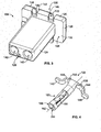
- FIG. 1 is a front perspective view of a connector system 100 formed in accordance with one embodiment.
- the connector system 100 includes a substrate 102 and a connector assembly 104 mounted to the substrate 102.
- a cable or wire 106 is directly terminated to the connector assembly 104.
- the connector assembly 104 is a poke-in type of connector, where the wire 106 is coupled to the connector assembly 104 by a simple poke-in wire termination.
- the poke-in termination offers quick and reliable wire termination as a low-labor alternative to hand-soldering of the wire 106 either directly to the substrate 102 or to a contact or other component.
- the connector system 100 may be part of a lighting system, such as an LED lighting system.
- a lighting system such as an LED lighting system.
- one or more LEDs 108 may be mounted to the substrate 102 in the vicinity of the connector assembly 104.
- the substrate 102 may be referred to hereinafter as an LED circuit board 102.
- the connector assembly 104 may be electrically connected to the LEDs 108 by traces 110 on the substrate 102.
- the connector assembly 104 supplies power and/or control functions to the LEDs 108.
- the wire 106 supplies power to the connector assembly 104.
- the connector system 100 may have use in other fields or for other applications in alternative embodiments other than supplying power to LEDs.
- the substrate 102 includes a front side 112 and a rear side 114.
- An opening 116 (shown in Figure 5 ) extends through the substrate 102 between the front and rear sides 112, 114.
- the LEDs 108 and traces 110 are routed along the front side 112.
- the substrate 102 is a substantially flat supporting layer that may mechanically support the connector assembly 104 and may electrically connect the connector assembly 104 with one or more peripheral devices, including the LEDs 108 via the traces 110.
- the substrate 102 may include a metal clad circuit board having an aluminum base or other metal base that provides very efficient thermal heat dissipation, such as for the LEDs 108.
- Other embodiments of the substrate 102 may be used in one or more alternative embodiments, such as an FR4 circuit board.
- the connector assembly 104 is electrically connected to the substrate 102 at the front side 112, such as at mounting pads 118 on the front side 112.
- the connector assembly 104 extends through the opening 116 to the rear side 114.
- the housing 120 at least partially protrudes through the opening 116 such that the bottom of the housing 120 is located proximate to and past the rear side 114 of the substrate 102.
- the bottom of the housing 120 is substantially flush with the rear side 114 of the substrate 102.
- the bottom of the housing 120 is partially recessed in the opening 116.
- the wire 106 is terminated to the connector assembly 104 at the rear side 114.
- the wire 106 may be loaded into the connector assembly 104 through the rear side 114.
- Such a system allows the wire 106 to remain in the fixture or recessed can that holds the connector system 100, which makes for easier, more direct termination by reducing routing of the wire 106.
- Such a system keeps the wire 106 on the rear side 114 of the substrate 102.
- the wire 106 does not need to be routed to the front side 112 to make an electrical connection to the substrate 102 or a connector on the front side 112.
- the wire 106 is thus not routed near the LEDs 108.
- the wire 106 does not block the light produced by the LEDs 108.
- the connector assembly 104 has a low profile so as to not detrimentally affect the lighting pattern of the LEDs 108.
- the profile of the connector assembly 104 is controllable, as compared to, for example, random routing of the wire 106 along the front side 112.
- the connector assembly 104 includes a housing 120 and one or more poke-in contacts 122.
- the connector assembly 104 includes two poke-in contacts 122, however any number of poke-in contacts 122 may be utilized.
- the poke-in contacts 122 are mounted to the front side 112 of the substrate 102 and the poke-in contacts 122 receive corresponding wires 106 from the rear side 114 of the substrate 102.
- the housing 120 extends through the opening 116 in the substrate 102, positioning the housing 120 on both sides 112, 114 of the substrate 102. Having the housing 120 extending through the substrate 102 allows the termination of the poke-in contacts 122 on the front side 112 while still allowing the termination to the wires 106 on the rear side 114.
- the connector system 100 is arranged such that the substrate 102 is oriented generally horizontally with the housing 120 extending generally vertically or generally perpendicularly through the substrate 102.
- the front side 112 is positioned generally vertically above the rear side 114.
- the LEDs 108 are positioned on the top and the wire 106 is loaded into the connector assembly 104 from the bottom.
- the wire loading direction is oriented generally vertically.
- Such orientation is merely one example of a possible orientation, but it is realized that other orientations are possible, including an orientation that was rotated 180° with the LEDs 108 positioned on the bottom, an orientation that was rotated 90° with the substrate 102 oriented vertically, or other orientations.
- the description herein will be with reference to an orientation with the substrate 102 being horizontal and the LEDs 108 on the top.
- FIG 2 is a top perspective view of the connector assembly 104.
- Figure 3 is a bottom perspective view of the connector assembly 104.
- the housing 120 includes a body 124 and a head 126.
- the body 124 extends from the head 126 to a bottom 128 of the housing 120.
- a top 130 of the housing 120 is defined by the head 126 generally opposite to the body 124.
- the head 126 is wider than the body 124 in at least one dimension (e.g. longitudinally and/or laterally).
- the body 124 is sized to extend through the opening 116 in the substrate 102 (both shown in Figure 1 ).
- the head 126 is sized larger than the opening 116 and is configured to be seated against the front side 112 (shown in Figure 1 ) of the substrate 102 when the body 124 is loaded into the opening 116.
- the head 126 may limit how far the housing 120 may be inserted into the opening 116.
- the housing 120 includes and/or is formed from a dielectric material, such as a plastic material.
- the head 126 includes a ledge 132 along a head bottom 134, which is defined by the bottom surface of the head 126 generally opposite the top 130.
- the ledge 132 extends to the body 124.
- the ledge 132 is downward facing and is configured to face and/or abut against the front side 112.
- the ledge 132 faces the bottom 128 of the housing 120.
- the housing 120 includes contact channels 140 extending therethrough that receive the poke-in contacts 122.
- the contact channels 140 extend entirely through the housing 120 and are open at the top 130 and the bottom 128.
- the contact channels 140 receive the poke-in contacts 122 through the top 130.
- the contact channels 140 receive the wires 106 (shown in Figure 1 ) through the bottom 128.
- the contact channels 140 are sized and shaped to hold the poke-in contacts 122.
- the contact channels 140 are sized and shaped to receive and guide the wires 106 to the poke-in contacts 122.
- the housing 120 includes contact slots 142 at the top 130.
- the contact slots 142 receive portions of the poke-in contacts 122.
- the poke-in contacts 122 have one or more mounting legs 144.
- the mounting legs 144 are used to mechanically and electrically couple the poke-in contacts 122 to the substrate 102.
- the mounting legs 144 may be soldered to the substrate 102.
- the contact slots 142 receive the mounting legs 144.
- the contact slots 142 extend from the contact channels 140 to outer edges 146 of the housing 120.
- the contact slots 142 allow the mounting legs 144 to be routed from the contact channels 140 to the outer edges 146.
- the mounting legs 144 have mounting surfaces 148 that are oriented for termination to the corresponding mounting pads 118.
- the mounting surfaces 148 are oriented generally coplanar with the ledge 132 at the head bottom 134 for mounting to the front side 112 of the substrate 102.
- the mounting surfaces 148 face the bottom 128 of the housing 120.
- the poke-in contacts 122 have locking barbs 150 extending therefrom that dig into the housing 120 within the contact slots 142 to hold the poke-in contacts 122 in the contact slots 142.
- the locking barbs 150 provide holding force to hold the poke-in contacts 122 in the contact slots 142 during mounting of the connector assembly 104 to the substrate 102.
- the locking barbs 150 provide holding force to hold the poke-in contacts 122 in the contact slots 142 during insertion of the wire 106 into the contact channels 140.
- Other types of securing features may be used in alternative embodiments to hold the poke-in contacts 122 in the housing 120.
- FIG 4 is a bottom perspective view of the poke-in contact 122.
- the poke-in contact 122 includes a wire trap 160 configured to receive the wire 106 (shown in Figure 1 ) to electrically connect the poke-in contact 122 to the wire 106.
- a pair of mounting legs 144 extends from the wire trap 160 at a top of the poke-in contact 122. Any number of mounting legs 144 may be provided, including a single mounting leg 144.
- the locking barbs 150 extend from the mounting legs 144 at the top. The locking barbs 150 may be provided at different locations in alternative embodiments.
- the wire trap 160 generally extends along a longitudinal axis 162 from the mounting legs 144 at the top to a wire receiving end 164 at a bottom of the wire trap 160.
- the wire trap 160 includes a barrel 166 configured to receive the wire 106 therein.
- the wire trap 160 includes a spring finger 168 extending into the barrel 166 to engage the wire 106 when the wire 106 is loaded into the barrel 166.
- the spring finger 168 is held against the wire 106 by a spring force to ensure electrical contact with the wire 106.
- multiple spring fingers 168 may extend into the barrel 166 to engage different sides of the wire 106. The end of the spring finger 168 may dig into the wire 106 to resist pull out of the wire 106.
- the poke-in contact 122 is stamped and formed.
- the barrel 166 is shaped by bending two edges of the poke-in contact 122 into a barrel shape to meet at a seam.
- the spring finger 168 may be generally opposite the seam. The spring finger 168 is stamped out of the poke-in contact 122 and bent inward into the barrel 166.
- the mounting legs 144 are bent or shaped such that the mounting surfaces 148 are oriented along a plane generally perpendicular to the longitudinal axis 162.
- the mounting legs 144 may define spring legs that are configured to be held against the substrate 102 by a spring force.
- the mounting legs 144 may be slightly angled downward, such that the mounting legs 144 are deflected upward when mounted to the substrate 102.
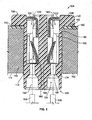
- Figure 5 is a cross-sectional view of the connector assembly 104.
- the poke-in contacts 122 are loaded into the contact channels 140.
- the poke-in contacts 122 are loaded into the contact channels 140 through the top 130.
- the mounting legs 144 extend along the head 126.
- the wire traps 160 are loaded into the contact channels 140 and are located in the body 124.
- the substrate 102 is illustrated in Figure 5 , showing the connector assembly 104 loaded through the opening 116.
- the opening 116 is defined by walls 180 of the substrate 102.
- the housing 120 includes substrate engagement surfaces 182 that engage the substrate 102.
- the substrate engagement surfaces 182 extend along the body 124.
- the body 124 is generally positioned within the plane of the substrate 102, but may extend beyond the rear side 114.
- the wire traps 160 when loaded into the body 124 are aligned with the plane of the substrate 102 (e.g. vertically aligned).
- the barrels 166 and spring fingers 168 are positioned between the front and rear sides 112, 114.
- the wire traps 160 may only be partially aligned with the plane of the substrate 102, with a portion of the wire traps 160 extending beyond the rear side 114. In other alternative embodiments, the wire traps 160 may not be aligned with the substrate 102, but rather the entire wire traps 160 are positioned beyond the rear side 114.
- the contact channels 140 are sized and shaped to guide the wires 106 into the wire traps 160.
- the contact channels 140 include funnels 184 that receive the wires 106 and guide the wires 106 into ports 186 that are generally centered along the contact channels 140.
- the ports 186 may have smaller diameters than other portions of the contact channels 140 to locate the wires 106 along the longitudinal axes 162 of the poke-in contacts 122.
- the ports 186 position the wires 106 to ensure that the wires 106 will engage the spring fingers 168 when pushed into the connector assembly 104.
- the ports 186 may have diameters that are approximately equal to the diameters of the wires 106 such that the wires 106 are somewhat restricted from movement (e.g. side-to-side) within the connector assembly 104.
- a connector assembly 104 is provided that is inverted such that the connector assembly 104 extends through the substrate 102.
- the connector assembly 104 is thus mounted to the front side 112 but yet is also accessible at the rear side 114 for termination to the wire 106.
- the connector assembly 104 utilizes the poke-in contacts 122 for quick termination of the wire 106 to the connector assembly 104.
- the wire 106 remains on the rear side 114 of the substrate 102 and does not block other components on the front side 112, such as the lighting pattern of the LEDs 108 on the front side 112.
- Figure 6 is a top perspective view of a connector system 200 formed in accordance with one embodiment.
- Figure 7 is a bottom perspective view of the connector system 200.
- the connector system 200 is another example of a connector system and is similar to the connector system 100 (shown in Figure 1 ) and may include similar components.
- the connector system 200 includes a heat sink 201, a substrate 202 mounted to the heat sink 201 and a connector assembly 204 mounted to the substrate 202.
- a driver card 206 is directly terminated to the connector assembly 204 to supply power to the substrate 202.
- the connector assembly 204 is a card edge type of connector, where an edge of the driver card 206 is plugged directly into the connector assembly 204, which may define a separable mating interface.
- the card edge termination offers quick and reliable power termination, which may be accomplished by an automated process and as a low-labor alternative to hand-soldering of wires directly to the substrate 202 or to a contact or other component of the substrate 202.
- the connector system 200 may be part of a lighting system, such as an LED lighting system.
- the substrate 202 may be an LED circuit board with one or more LEDs 208 mounted to the LED circuit board.
- the substrate 202 may be referred to hereinafter as an LED circuit board.
- the connector assembly 204 supplies power and/or control functions to the LEDs 208.
- the driver card 206 supplies power to the connector assembly 204.
- the connector system 200 may have use in other fields or for other applications in alternative embodiments other than supplying power to LEDs.
- the heat sink 201 dissipates heat from the components mounted to the LED circuit board 202, such as the LEDs 208.
- the LED circuit board 202 includes a front side 212 and a rear side 214.
- the front side 212 defines a top
- the rear side 214 defines a bottom. While components described herein may be referred to as top or bottom, such labels are merely descriptive of the orientation shown in Figure 6 and the system may be utilized (e.g. mounted in a fixture) with a component referred to as "top” positioned vertically below a component referred to as "bottom”, and vice versa.
- An opening 216 extends through the LED circuit board 202 between the front and rear sides 212, 214.
- the LEDs 208 and corresponding traces are routed along the front side 212.
- the LED circuit board 202 is a substantially flat supporting layer that may mechanically support the connector assembly 204 and may electrically connect the connector assembly 204 with one or more peripheral devices, including the LEDs 208.
- the LED circuit board 202 may include a metal clad circuit board having an aluminum base or other metal base that provides very efficient thermal heat dissipation, such as for the LEDs 208, to the heat sink 201.
- Other embodiments of the LED circuit board 202 may be used in one or more alternative embodiments, such as an FR4 circuit board.
- the connector assembly 204 is electrically connected to the LED circuit board 202 at the front side 212, such as at mounting pads 218 on the front side 212.
- a cover or cap may be provided and secured over the top of the connector assembly 204, such as to cover the contacts 222.
- the cover may be coupled to the head of the housing 220.
- the cover may be latched to the housing 220.
- the cover may cover the exposed portions of the contacts 222 to limit unintentional touching of the contacts 222.
- the connector assembl 204 extends through the opening 216 to the rear side 214.
- the housing 220 at least partially protrudes through the opening 216 such that the bottom of the housing 220 is located proximate to and past the rear side 214 of the LED circuit board 202 and at or past a rear side of the heat sink 201.
- the bottom of the housing 220 is substantially flush with the rear side 214 of the LED circuit board 202 or the rear side of the heat sink 201.
- the bottom of the housing 220 is partially recessed in the opening 216 or in the heat sink 201.
- the driver card 206 is terminated to the connector assembly 204 from the rear side 214.
- the driver card 206 may be loaded into the connector assembly 204 from underneath the heat sink 201 and the LED circuit board 202.
- Such a system allows the driver card 206 to remain in the fixture or recessed can that holds the connector system 200, which makes for easier, more direct termination by reducing routing of wire or other components to the front side 212 of the LED circuit board 202.
- Such a system keeps the driver card, wires and other components on the rear side 214 of the LED circuit board 202. Wires do not need to be routed from the driver card 206 to the front side 212 to make an electrical connection to the LED circuit board 202 or a connector on the front side 212.
- Wires and other components are thus not routed or positioned near the LEDs 208.
- the light produced by the LEDs 208 is not blocked by other components or wires.
- the connector assembly 204 has a low profile so as to not detrimentally affect the lighting pattern of the LEDs 208.
- the profile of the connector assembly 204 is controllable and fixed in space by design, as compared to, for example, random routing of the wires along the front side 212.
- the connector assembly 204 includes a housing 220 and one or more contacts 222.
- the connector assembly 204 includes two contacts 222, however any number of contacts 222 may be utilized.
- the contacts 222 are mounted to the front side 212 of the LED circuit board 202 and the contacts 222 mate with the driver card 206.
- the housing 220 extends through the opening 216 in the LED circuit board 202, positioning the housing 220 on both sides 212, 214 of the LED circuit board 202. Having the housing 220 extending through the LED circuit board 202 allows the termination of the contacts 222 on the front side 212 while still allowing the power termination on the rear side 214.
- the connector system 200 is arranged such that the LED circuit board 202 is oriented generally horizontally with the driver card 206 extending generally vertically from the connector assembly 204.
- the front side 212 is positioned generally vertically above the rear side 214.
- the LEDs 208 are positioned on the top and the driver card 206 is loaded into the connector assembly 204 from the bottom.
- the wire loading direction is oriented generally vertically.
- Such orientation is merely one example of a possible orientation, but it is realized that other orientations are possible, including an orientation that is rotated 180° with the LEDs 208 positioned on the bottom, an orientation that is rotated 90° with the LED circuit board 202 oriented vertically, or other orientations.
- the description herein will be with reference to an orientation with the LED circuit board 202 being horizontal and the LEDs 208 on the top.
- FIG 8 is a top perspective view of the connector assembly 204.
- Figure 9 is a bottom perspective view of the connector assembly 204.
- the housing 220 includes a body 224 and a head 226.
- the body 224 extends from the head 226 to a bottom 228 of the housing 220.
- a top 230 of the housing 220 is defined by the head 226 generally opposite to the body 224.
- the head 226 is wider than the body 224 in at least one dimension (e.g. longitudinally and/or laterally).
- the body 224 is sized to extend through the opening 216 in the LED circuit board 202 (both shown in Figure 6 ).
- the head 226 is sized larger than the opening 216 and is configured to be seated against the front side 212 (shown in Figure 6 ) of the LED circuit board 202 when the body 224 is loaded into the opening 216.
- the head 226 may limit how far the housing 220 may be inserted into the opening 216.
- the housing 220 includes and/or is formed from a dielectric material, such as a plastic material.
- the head 226 includes a ledge 232 along a head bottom 234, which is defined by the bottom surface of the head 226 generally opposite the top 230.
- the ledge 232 extends to the body 224.
- the ledge 232 is downward facing and is configured to face and/or abut against the front side 212.
- the ledge 232 faces the bottom 228 of the housing 220.
- the housing 220 includes contact channels 240 extending therethrough that receive the contacts 222.
- the contact channels 240 extend entirely through the housing 220 and are open at the top 230 and the bottom 228.
- the contact channels 240 receive the contacts 222 through the top 230.
- the contact channels 240 are sized and shaped to hold the contacts 222.
- the contact channels 240 are open to a driver card slot 250 at the bottom 228.
- the driver card slot 250 is sized and shaped to receive the driver card 206 (shown in Figure 2 ) therein. Any number of contacts 222 and contact channels 240 may be provided.
- the housing 220 includes contact slots 242 at the top 230.
- the contact slots 242 receive portions of the contacts 222.
- the contacts 222 have one or more mounting legs 244.
- the mounting legs 244 are used to mechanically and electrically couple the contacts 222 to the LED circuit board 202.
- the mounting legs 244 may be soldered to the LED circuit board 202.
- the contact slots 242 receive the mounting legs 244.
- the contact slots 242 extend from the contact channels 240 to an outer edge 246 of the housing 220. In the illustrated embodiment, the contact slots 242 extend in the same direction such that the mounting legs 244 extend to the same edge 246 of the housing 220.
- the mounting legs 244 have mounting surfaces 248 that are oriented for termination to the corresponding mounting pads 218.
- the mounting surfaces 248 are oriented generally coplanar with the ledge 232 at the head bottom 234 for mounting to the front side 212 of the LED circuit board 202.
- the mounting surfaces 248 face the bottom 228 of the housing 220.
- Each contact 222 includes a spring beam 260 opposite the mounting leg 244.
- the spring beam 260 is configured to be spring biased against the driver card 206 (shown in Figure 6 ) when the driver card 206 is loaded into the driver card slot 250 to electrically connect the contact 222 to the driver card 206.
- the spring beam 260 forms a separable mating interface with the driver card 206.
- the spring beams 260 are deflectable in the driver card slot 250.
- the housing 220 may include pockets 262 that allow the spring beams 260 to deflect outward when the driver card 206 is loaded into the driver card slot 250.
- the housing 220 holds a hold down tab 264 in the head 226.
- the hold down tab 264 is exposed along the head bottom 234 for securing the connector assembly 204 to the LED circuit board 202.
- the hold down tab 264 is configured to be soldered to the LED circuit board 202 to secure the connector assembly 204 to the LED circuit board 202. Any number of hold down tabs 264 may be provided. Other types of securing features may be used in alternative embodiments to secure the connector assembly 204 to the LED circuit board 202.
- Figure 10 is a cross-sectional view of the connector assembly 204.
- the contacts 222 are loaded into the contact channels 240.
- the contacts 222 are loaded into the contact channels 240 through the top 230.
- the mounting legs 244 extend along the head 226.
- the spring beams 260 are loaded into the contact channels 240 and are located in the driver card slot 250 in the body 224.
- the driver card slot 250 is defined by side walls 270 and an inner wall 272 opposite an opening 274 in the bottom 228 of the housing 220, through which the driver card 206 (shown in Figure 6 ) is loaded into the driver card slot 250.
- the contact channels 240 are open to the driver card slot 250 allowing the contacts 222 to extend into the driver card slot 250 from the contact channels 240.
- the housing 220 includes a polarization feature 276 in the driver card slot 250.
- the polarization feature 276 is defined by a non-uniform shape of the driver card slot 250.
- the inner wall 272 is not straight, but rather has a portion that is offset and further recessed from the bottom 228. Having a portion of the driver card slot 250 stepped inward allows the driver card 206 to be inserted in a single orientation.
- the step back in the driver card slot 250 exposes more of one of the contacts 222 as compared to the other contact 222. A greater length of one of the contacts 222 is exposed in the driver card slot 250 as compared to the length that the other contact 222 is exposed.
- the housing 220 includes a latch 278 in the driver card slot 250.
- the latch 278 is used to secure the driver card 206 in the driver card slot 250.
- the latch 278 is defined by an undercut 280 extending between the offset portions of the inner wall 272.
- the undercut 280 has a slant surface 282 that is angled transverse to the loading direction.
- a portion of the driver card 206 is configured to be captured in the undercut 280 by the slant surface 282.
- the nose of the latch 278 may be rounded to allow for easier insertion of the driver card 206 into the driver card slot 250.
- Other types of securing features may be used other than a latch.
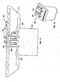
- FIG 11 illustrates a portion of the driver card 206.
- the driver card 206 includes a mating extension 284 configured to be plugged into the driver card slot 250 (shown in Figure 10 ).
- the driver card 206 includes power pads 286 on the mating extension 284.
- the power pads 286 are configured to be mated with the contacts 222 (shown in Figure 10 ) when the driver card 206 is loaded into the driver card slot 250.
- the power pads 286 may be staggered (e.g. one of the power pads 286 may be positioned closer to a front edge 288 of the driver card 206) to allow for sequenced mating with the contacts 222.
- the driver card 206 includes a latch 290 for securing the driver card 206 in the driver card slot 250.
- the latch 290 is defined by an undercut 292 defined by a staggered front edge 288.
- the undercut 292 has a slant surface 294 that is angled transverse to the loading direction of the driver card 206.
- the latch 290 is configured to be captured in the undercut 280 (shown in Figure 10 ) when the driver card 206 is loaded in the driver card slot 250.
- the nose of the latch 290 may be rounded to allow for easier insertion of the driver card 206 into the driver card slot 250.
- Other types of securing features may be used other than a latch.
- Figure 12 is a cross-sectional view of the connector system 200, showing the driver card 206 loaded into the connector assembly 204.
- the contacts 222 engage the power pads 286 to create a power path from the driver card 206 to the LED circuit board 202.
- stops 295 may be provided to limit insertion of the driver card 206 into the connector assembly 204, such as to ensure that the connector assembly 204 is not pushed off of the LED circuit board 202 during mating.
- the stops 295 may be positioned between the driver card 206 and the bottom of the heat sink 201.
- the stops 295 may be part of the driver card 206, such as defined by the board of the driver card 206 or separate components mounted to the driver card 206.
- the stops 295 may be part of the heat sink 201 or coupled to the heat sink 201.
- the connector assembly 204 is shown loaded through the opening 216 in the LED circuit board 202 and loaded through an opening 296 in the heat sink 201.
- the openings 216, 296 are defined by internal walls.
- the housing 220 includes engagement surfaces 298 that engage the LED circuit board 202 and the heat sink 201 along the internal walls of the openings 216, 296.
- the engagement surfaces 298 extend along the body 224.
- the body 224 is generally positioned within the plane of the LED circuit board 202 and the heat sink 201, and may extend beyond the bottoms thereof.
- the spring beams 260 when loaded into the body 224, are aligned with the plane of the LED circuit board 202 and the plane of the heat sink 201 (e.g. vertically aligned).
- FIG 13 illustrate another connector assembly 304 formed in accordance with an exemplary embodiment.
- the connector assembly 304 is similar to the connector assembly 204 (shown in Figure 6 ), however the connector assembly 304 is configured to be terminated directly to wires.
- the connector assembly 304 includes contacts 322 that are poke-in type contacts (similar to the poke-in type contacts 122 of Figure 1 ) that have wire barrels that receive ends of wires therein. Any number of contacts 322 may be used.
- the connector assembly 304 may have similar dimensions and mounting features as the connector assembly 204 for mounting to the LED circuit board 202 (shown in Figure 6 ).
- the mounting legs of the contacts 322 may be identical to the mounting legs of the contacts 222 (shown in Figure 6 ).
Abstract
Description
- The subject matter herein relates generally to connector assemblies for connector systems.
- Many known connectors are mounted on a top side of a circuit board and protrude upward from the circuit board. These connectors include electrical contacts that are electrically connected to conductive traces in the circuit board or to wires that extend along the surface and/or sides of the circuit board. The connectors have a mating interface configured to mate with a mating connector. The mating interface typically is located parallel or perpendicular with respect to the top side of the circuit board.
- These known connectors may have a height profile above the top side of the circuit board that is too large for certain applications. For example, the profile of many connectors used in conjunction with light emitting diodes ("LEDs") may be so large relative to the LEDs that the connectors impede or block some of the light emitted by the LEDs. Additionally, the trend towards smaller electronic devices and more densely packed electronic devices and connectors on a circuit board requires the reduction of the height profile for connectors.
- The problem to be solved is a need for a connector having a smaller profile than known connectors. Such a connector may be useful in devices where a smaller connector height profile is desired, such as in LED lighting devices.
- The solution is provided by a connector assembly for mounting to a substrate having an opening extending between a front side and a rear side. The connector assembly includes a housing having a body at a bottom of the housing and a head at a top of the housing. The head extends from the body and is wider than the body. The head is configured to be mounted to the front side of the substrate with the body extending through the opening of the substrate to the rear side of the substrate. The housing has a contact channel extending therethrough that is open at the top and the bottom of the housing. The connector assembly includes a poke-in contact received in the contact channel. The poke-in contact has a wire trap configured to receive a wire therein in a wire loading direction through the bottom of the housing from the rear side of the substrate. The poke-in contact has a mounting leg extending from the head that is configured to be mounted to the front side of the substrate.
- In addition, a connector assembly is provided for interconnecting an LED circuit board and a driver card supplying power to the LED circuit board. The connector assembly includes a housing having a body and a head extending outward from the body. The housing is coupled to the LED circuit board with the head mounted to a front side of the LED circuit board and with the body extending through an opening of the LED circuit board to a rear side of the LED circuit board. The housing has driver card slot in the body configured to receive the driver card therein in a loading direction from the rear side of the LED circuit board. The housing has a contact channel extending through the head and being open to the driver card slot. A contact is received in the contact channel. The contact has a mating interface configured to engage and be electrically connected to the driver card. The contact has a mounting leg extending from the head that is configured to be mounted to the front side of the LED circuit board.
- The invention will now be described by way of example with reference to the accompanying drawings in which:
-
Figure 1 is a front perspective view of a connector system formed in accordance with one embodiment. -
Figure 2 is a top perspective view of a connector assembly for the connector system. -
Figure 3 is a bottom perspective view of the connector assembly. -
Figure 4 is a bottom perspective view of a poke-in contact for the connector assembly. -
Figure 5 is a cross-sectional view of the connector assembly. -
Figure 6 is a top perspective view of a connector system formed in accordance with one embodiment. -
Figure 7 is a bottom perspective view of the connector system shown inFigure 6 . -
Figure 8 is a top perspective view of a connector assembly of the connector system shown inFigure 6 . -
Figure 9 is a bottom perspective view of the connector assembly shown inFigure 8 . -
Figure 10 is a cross-sectional view of the connector assembly shown inFigure 8 . -
Figure 11 illustrates a portion of a driver card of the connector system shown inFigure 6 . -
Figure 12 is a cross-sectional view of the connector system showing the driver card loaded into the connector assembly. -
Figure 13 illustrate a connector assembly formed in accordance with an exemplary embodiment. - In one embodiment, a connector assembly is provided for mounting to a substrate having an opening extending between a front side and a rear side. The connector assembly includes a housing having a body at a bottom of the housing and a head at a top of the housing. The head extends from the body and is wider than the body. The head is configured to be mounted to the front side of the substrate with the body extending through the opening of the substrate to the rear side of the substrate. The housing has a contact channel extending therethrough that is open at the top and the bottom of the housing. The connector assembly includes a poke-in contact received in the contact channel. The poke-in contact has a wire trap configured to receive a wire therein in a wire loading direction through the bottom of the housing from the rear side of the substrate. The poke-in contact has a mounting leg extending from the head that is configured to be mounted to the front side of the substrate.
- In a further embodiment, a connector assembly is provided for mounting to a substrate having an opening extending between a front side and a rear side. The connector assembly includes a housing configured to extend through the opening of the substrate such that a portion of the housing is forward of the front side of the housing and such that a portion of the housing is rearward of the rear side of the housing. The housing has a contact channel extending therethrough that is configured to receive a wire through a bottom of the housing. A poke-in contact is received in the contact channel. The poke-in contact has a wire trap configured to receive a wire therein in a wire loading direction from the rear side of the substrate. The poke-in contact has a mounting leg having a mounting surface. The mounting leg extends from the housing proximate to a top of the housing. The mounting surface is configured to be mounted to the front side of the substrate and faces the bottom of the housing.
- In another embodiment, a connector system is provided that includes a substrate having a front side and a rear side with an opening therethrough, and a connector assembly coupled to the substrate. The connector assembly includes a housing having a body at a bottom of the housing and a head at a top of the housing. The head extends along the front side of the substrate and the body extends from the head through the opening such that the bottom is rearward of the rear side. The housing has a contact channel extending therethrough that is open at the top and the bottom of the housing. A poke-in contact is received in the contact channel through the top of the housing. The poke-in contact has a wire trap configured to receive a wire therein in a wire loading direction through the bottom of the housing. The poke-in contact has a mounting leg extending from the head and mounted to the front side of the substrate.
- In a further embodiment, a connector assembly is provided for interconnecting an LED circuit board and a driver card supplying power to the LED circuit board. The connector assembly includes a housing having a body and a head extending outward from the body. The housing is coupled to the LED circuit board with the head mounted to a front side of the LED circuit board and with the body extending through an opening of the LED circuit board to a rear side of the LED circuit board. The housing has driver card slot in the body configured to receive the driver card therein in a loading direction from the rear side of the LED circuit board. The housing has a contact channel extending through the head and being open to the driver card slot. A contact is received in the contact channel. The contact has a mating interface configured to engage and be electrically connected to the driver card. The contact has a mounting leg extending from the head that is configured to be mounted to the front side of the LED circuit board.
- In another embodiment, a connector system is provided including an LED circuit board having a front side, a rear side and an opening extending therethrough. The LED circuit board has a mounting pad on the front side and at least one LED mounted on the front side. The connector system includes a driver card having a power supply and a power pad proximate to a mating edge of the driver card. The connector system includes a connector assembly coupled to the LED circuit board and receiving the driver card to supply power from the driver card to the LED circuit board. The connector assembly includes a housing having a body and a head extending outward from the body. The housing is coupled to the LED circuit board with the head mounted to the front side of the LED circuit board and with the body extending through the opening of the LED circuit board to the rear side of the LED circuit board. The housing has a driver card slot in the body receiving the driver card therein in a loading direction from the rear side of the LED circuit board. The housing has a contact channel extending through the head that is open to the driver card slot. A contact is received in the contact channel. The contact has a mating interface configured to engage and be electrically connected to the power pad of the driver card. The contact has a mounting leg extending from the head that is terminated to the mounting pad on the front side of the LED circuit board.
- In a further embodiment, a connector assembly is provided for mounting to a substrate having an opening extending between a front side and a rear side. The connector assembly includes a housing having a body at a bottom of the housing and a head at a top of the housing. The head extends from the body and is wider than the body and configured to be mounted to the front side of the substrate with the body extending through the opening of the substrate to the rear side of the substrate. The housing has a contact channel extending therethrough being open at the top and the bottom of the housing. A contact is received in the contact channel. The contact has a mating interface configured to engage and be electrically connected to a power conductor of a mating component loaded into the housing in a loading direction through the bottom of the housing from the rear side of the substrate. The contact has a mounting leg extending from the head that is configured to be mounted to the front side of the substrate.
-
Figure 1 is a front perspective view of aconnector system 100 formed in accordance with one embodiment. Theconnector system 100 includes asubstrate 102 and aconnector assembly 104 mounted to thesubstrate 102. A cable orwire 106 is directly terminated to theconnector assembly 104. In an exemplary embodiment, theconnector assembly 104 is a poke-in type of connector, where thewire 106 is coupled to theconnector assembly 104 by a simple poke-in wire termination. The poke-in termination offers quick and reliable wire termination as a low-labor alternative to hand-soldering of thewire 106 either directly to thesubstrate 102 or to a contact or other component. - In an exemplary embodiment, the
connector system 100 may be part of a lighting system, such as an LED lighting system. For example, one ormore LEDs 108 may be mounted to thesubstrate 102 in the vicinity of theconnector assembly 104. Thesubstrate 102 may be referred to hereinafter as anLED circuit board 102. Theconnector assembly 104 may be electrically connected to theLEDs 108 bytraces 110 on thesubstrate 102. Theconnector assembly 104 supplies power and/or control functions to theLEDs 108. Thewire 106 supplies power to theconnector assembly 104. Theconnector system 100 may have use in other fields or for other applications in alternative embodiments other than supplying power to LEDs. - The
substrate 102 includes afront side 112 and arear side 114. An opening 116 (shown inFigure 5 ) extends through thesubstrate 102 between the front andrear sides LEDs 108 and traces 110 are routed along thefront side 112. Thesubstrate 102 is a substantially flat supporting layer that may mechanically support theconnector assembly 104 and may electrically connect theconnector assembly 104 with one or more peripheral devices, including theLEDs 108 via thetraces 110. In an exemplary embodiment, thesubstrate 102 may include a metal clad circuit board having an aluminum base or other metal base that provides very efficient thermal heat dissipation, such as for theLEDs 108. Other embodiments of thesubstrate 102 may be used in one or more alternative embodiments, such as an FR4 circuit board. - The
connector assembly 104 is electrically connected to thesubstrate 102 at thefront side 112, such as at mountingpads 118 on thefront side 112. Theconnector assembly 104 extends through theopening 116 to therear side 114. In the illustrated embodiment, thehousing 120 at least partially protrudes through theopening 116 such that the bottom of thehousing 120 is located proximate to and past therear side 114 of thesubstrate 102. In another embodiment, the bottom of thehousing 120 is substantially flush with therear side 114 of thesubstrate 102. In another embodiment, the bottom of thehousing 120 is partially recessed in theopening 116. - The
wire 106 is terminated to theconnector assembly 104 at therear side 114. For example, thewire 106 may be loaded into theconnector assembly 104 through therear side 114. Such a system allows thewire 106 to remain in the fixture or recessed can that holds theconnector system 100, which makes for easier, more direct termination by reducing routing of thewire 106. Such a system keeps thewire 106 on therear side 114 of thesubstrate 102. Thewire 106 does not need to be routed to thefront side 112 to make an electrical connection to thesubstrate 102 or a connector on thefront side 112. Thewire 106 is thus not routed near theLEDs 108. Thewire 106 does not block the light produced by theLEDs 108. Theconnector assembly 104 has a low profile so as to not detrimentally affect the lighting pattern of theLEDs 108. The profile of theconnector assembly 104 is controllable, as compared to, for example, random routing of thewire 106 along thefront side 112. - The
connector assembly 104 includes ahousing 120 and one or more poke-incontacts 122. In the illustrated embodiment, theconnector assembly 104 includes two poke-incontacts 122, however any number of poke-incontacts 122 may be utilized. The poke-incontacts 122 are mounted to thefront side 112 of thesubstrate 102 and the poke-incontacts 122 receive correspondingwires 106 from therear side 114 of thesubstrate 102. Thehousing 120 extends through theopening 116 in thesubstrate 102, positioning thehousing 120 on bothsides substrate 102. Having thehousing 120 extending through thesubstrate 102 allows the termination of the poke-incontacts 122 on thefront side 112 while still allowing the termination to thewires 106 on therear side 114. - In an exemplary embodiment, the
connector system 100 is arranged such that thesubstrate 102 is oriented generally horizontally with thehousing 120 extending generally vertically or generally perpendicularly through thesubstrate 102. Thefront side 112 is positioned generally vertically above therear side 114. TheLEDs 108 are positioned on the top and thewire 106 is loaded into theconnector assembly 104 from the bottom. The wire loading direction is oriented generally vertically. Such orientation is merely one example of a possible orientation, but it is realized that other orientations are possible, including an orientation that was rotated 180° with theLEDs 108 positioned on the bottom, an orientation that was rotated 90° with thesubstrate 102 oriented vertically, or other orientations. The description herein will be with reference to an orientation with thesubstrate 102 being horizontal and theLEDs 108 on the top. -
Figure 2 is a top perspective view of theconnector assembly 104.Figure 3 is a bottom perspective view of theconnector assembly 104. Thehousing 120 includes abody 124 and ahead 126. Thebody 124 extends from thehead 126 to abottom 128 of thehousing 120. A top 130 of thehousing 120 is defined by thehead 126 generally opposite to thebody 124. Thehead 126 is wider than thebody 124 in at least one dimension (e.g. longitudinally and/or laterally). Thebody 124 is sized to extend through theopening 116 in the substrate 102 (both shown inFigure 1 ). Thehead 126 is sized larger than theopening 116 and is configured to be seated against the front side 112 (shown inFigure 1 ) of thesubstrate 102 when thebody 124 is loaded into theopening 116. Thehead 126 may limit how far thehousing 120 may be inserted into theopening 116. In an exemplary embodiment, thehousing 120 includes and/or is formed from a dielectric material, such as a plastic material. - The
head 126 includes aledge 132 along ahead bottom 134, which is defined by the bottom surface of thehead 126 generally opposite the top 130. Theledge 132 extends to thebody 124. Theledge 132 is downward facing and is configured to face and/or abut against thefront side 112. Theledge 132 faces thebottom 128 of thehousing 120. - The
housing 120 includescontact channels 140 extending therethrough that receive the poke-incontacts 122. In an exemplary embodiment, thecontact channels 140 extend entirely through thehousing 120 and are open at the top 130 and the bottom 128. Thecontact channels 140 receive the poke-incontacts 122 through the top 130. Thecontact channels 140 receive the wires 106 (shown inFigure 1 ) through the bottom 128. Thecontact channels 140 are sized and shaped to hold the poke-incontacts 122. Thecontact channels 140 are sized and shaped to receive and guide thewires 106 to the poke-incontacts 122. - The
housing 120 includescontact slots 142 at the top 130. Thecontact slots 142 receive portions of the poke-incontacts 122. In an exemplary embodiment, the poke-incontacts 122 have one or more mountinglegs 144. The mountinglegs 144 are used to mechanically and electrically couple the poke-incontacts 122 to thesubstrate 102. For example, the mountinglegs 144 may be soldered to thesubstrate 102. Thecontact slots 142 receive the mountinglegs 144. Thecontact slots 142 extend from thecontact channels 140 toouter edges 146 of thehousing 120. Thecontact slots 142 allow the mountinglegs 144 to be routed from thecontact channels 140 to the outer edges 146. The mountinglegs 144 have mountingsurfaces 148 that are oriented for termination to the corresponding mountingpads 118. In an exemplary embodiment, the mountingsurfaces 148 are oriented generally coplanar with theledge 132 at thehead bottom 134 for mounting to thefront side 112 of thesubstrate 102. The mountingsurfaces 148 face thebottom 128 of thehousing 120. - In an exemplary embodiment, the poke-in
contacts 122 have lockingbarbs 150 extending therefrom that dig into thehousing 120 within thecontact slots 142 to hold the poke-incontacts 122 in thecontact slots 142. The lockingbarbs 150 provide holding force to hold the poke-incontacts 122 in thecontact slots 142 during mounting of theconnector assembly 104 to thesubstrate 102. The lockingbarbs 150 provide holding force to hold the poke-incontacts 122 in thecontact slots 142 during insertion of thewire 106 into thecontact channels 140. Other types of securing features may be used in alternative embodiments to hold the poke-incontacts 122 in thehousing 120. -
Figure 4 is a bottom perspective view of the poke-incontact 122. The poke-incontact 122 includes awire trap 160 configured to receive the wire 106 (shown inFigure 1 ) to electrically connect the poke-incontact 122 to thewire 106. A pair of mountinglegs 144 extends from thewire trap 160 at a top of the poke-incontact 122. Any number of mountinglegs 144 may be provided, including a single mountingleg 144. The lockingbarbs 150 extend from the mountinglegs 144 at the top. The lockingbarbs 150 may be provided at different locations in alternative embodiments. - The
wire trap 160 generally extends along alongitudinal axis 162 from the mountinglegs 144 at the top to awire receiving end 164 at a bottom of thewire trap 160. Thewire trap 160 includes abarrel 166 configured to receive thewire 106 therein. Thewire trap 160 includes aspring finger 168 extending into thebarrel 166 to engage thewire 106 when thewire 106 is loaded into thebarrel 166. Thespring finger 168 is held against thewire 106 by a spring force to ensure electrical contact with thewire 106. Optionally,multiple spring fingers 168 may extend into thebarrel 166 to engage different sides of thewire 106. The end of thespring finger 168 may dig into thewire 106 to resist pull out of thewire 106. In an exemplary embodiment, the poke-incontact 122 is stamped and formed. Thebarrel 166 is shaped by bending two edges of the poke-incontact 122 into a barrel shape to meet at a seam. Optionally, thespring finger 168 may be generally opposite the seam. Thespring finger 168 is stamped out of the poke-incontact 122 and bent inward into thebarrel 166. - The mounting
legs 144 are bent or shaped such that the mountingsurfaces 148 are oriented along a plane generally perpendicular to thelongitudinal axis 162. The mountinglegs 144 may define spring legs that are configured to be held against thesubstrate 102 by a spring force. Optionally, the mountinglegs 144 may be slightly angled downward, such that the mountinglegs 144 are deflected upward when mounted to thesubstrate 102. -
Figure 5 is a cross-sectional view of theconnector assembly 104. The poke-incontacts 122 are loaded into thecontact channels 140. In an exemplary embodiment, the poke-incontacts 122 are loaded into thecontact channels 140 through the top 130. The mountinglegs 144 extend along thehead 126. The wire traps 160 are loaded into thecontact channels 140 and are located in thebody 124. - The
substrate 102 is illustrated inFigure 5 , showing theconnector assembly 104 loaded through theopening 116. Theopening 116 is defined bywalls 180 of thesubstrate 102. Thehousing 120 includes substrate engagement surfaces 182 that engage thesubstrate 102. The substrate engagement surfaces 182 extend along thebody 124. Thebody 124 is generally positioned within the plane of thesubstrate 102, but may extend beyond therear side 114. In an exemplary embodiment, the wire traps 160, when loaded into thebody 124 are aligned with the plane of the substrate 102 (e.g. vertically aligned). For example, thebarrels 166 andspring fingers 168 are positioned between the front andrear sides substrate 102, with a portion of the wire traps 160 extending beyond therear side 114. In other alternative embodiments, the wire traps 160 may not be aligned with thesubstrate 102, but rather the entire wire traps 160 are positioned beyond therear side 114. - The
contact channels 140 are sized and shaped to guide thewires 106 into the wire traps 160. At the bottom 128, thecontact channels 140 includefunnels 184 that receive thewires 106 and guide thewires 106 intoports 186 that are generally centered along thecontact channels 140. Theports 186 may have smaller diameters than other portions of thecontact channels 140 to locate thewires 106 along thelongitudinal axes 162 of the poke-incontacts 122. Theports 186 position thewires 106 to ensure that thewires 106 will engage thespring fingers 168 when pushed into theconnector assembly 104. Theports 186 may have diameters that are approximately equal to the diameters of thewires 106 such that thewires 106 are somewhat restricted from movement (e.g. side-to-side) within theconnector assembly 104. - A
connector assembly 104 is provided that is inverted such that theconnector assembly 104 extends through thesubstrate 102. Theconnector assembly 104 is thus mounted to thefront side 112 but yet is also accessible at therear side 114 for termination to thewire 106. Theconnector assembly 104 utilizes the poke-incontacts 122 for quick termination of thewire 106 to theconnector assembly 104. Thewire 106 remains on therear side 114 of thesubstrate 102 and does not block other components on thefront side 112, such as the lighting pattern of theLEDs 108 on thefront side 112. -
Figure 6 is a top perspective view of aconnector system 200 formed in accordance with one embodiment.Figure 7 is a bottom perspective view of theconnector system 200. Theconnector system 200 is another example of a connector system and is similar to the connector system 100 (shown inFigure 1 ) and may include similar components. - The
connector system 200 includes aheat sink 201, asubstrate 202 mounted to theheat sink 201 and aconnector assembly 204 mounted to thesubstrate 202. Adriver card 206 is directly terminated to theconnector assembly 204 to supply power to thesubstrate 202. In an exemplary embodiment, theconnector assembly 204 is a card edge type of connector, where an edge of thedriver card 206 is plugged directly into theconnector assembly 204, which may define a separable mating interface. The card edge termination offers quick and reliable power termination, which may be accomplished by an automated process and as a low-labor alternative to hand-soldering of wires directly to thesubstrate 202 or to a contact or other component of thesubstrate 202. - In an exemplary embodiment, the
connector system 200 may be part of a lighting system, such as an LED lighting system. For example, thesubstrate 202 may be an LED circuit board with one ormore LEDs 208 mounted to the LED circuit board. Thesubstrate 202 may be referred to hereinafter as an LED circuit board. Theconnector assembly 204 supplies power and/or control functions to theLEDs 208. Thedriver card 206 supplies power to theconnector assembly 204. Theconnector system 200 may have use in other fields or for other applications in alternative embodiments other than supplying power to LEDs. Theheat sink 201 dissipates heat from the components mounted to theLED circuit board 202, such as theLEDs 208. - The
LED circuit board 202 includes afront side 212 and arear side 214. In the orientation shown inFigure 6 , thefront side 212 defines a top and therear side 214 defines a bottom. While components described herein may be referred to as top or bottom, such labels are merely descriptive of the orientation shown inFigure 6 and the system may be utilized (e.g. mounted in a fixture) with a component referred to as "top" positioned vertically below a component referred to as "bottom", and vice versa. - An opening 216 (shown in
Figure 6 ) extends through theLED circuit board 202 between the front andrear sides LEDs 208 and corresponding traces are routed along thefront side 212. TheLED circuit board 202 is a substantially flat supporting layer that may mechanically support theconnector assembly 204 and may electrically connect theconnector assembly 204 with one or more peripheral devices, including theLEDs 208. In an exemplary embodiment, theLED circuit board 202 may include a metal clad circuit board having an aluminum base or other metal base that provides very efficient thermal heat dissipation, such as for theLEDs 208, to theheat sink 201. Other embodiments of theLED circuit board 202 may be used in one or more alternative embodiments, such as an FR4 circuit board. - The
connector assembly 204 is electrically connected to theLED circuit board 202 at thefront side 212, such as at mountingpads 218 on thefront side 212. Optionally, a cover or cap may be provided and secured over the top of theconnector assembly 204, such as to cover thecontacts 222. The cover may be coupled to the head of thehousing 220. The cover may be latched to thehousing 220. The cover may cover the exposed portions of thecontacts 222 to limit unintentional touching of thecontacts 222. Theconnector assembl 204 extends through theopening 216 to therear side 214. In the illustrated embodiment, thehousing 220 at least partially protrudes through theopening 216 such that the bottom of thehousing 220 is located proximate to and past therear side 214 of theLED circuit board 202 and at or past a rear side of theheat sink 201. In another embodiment, the bottom of thehousing 220 is substantially flush with therear side 214 of theLED circuit board 202 or the rear side of theheat sink 201. In another embodiment, the bottom of thehousing 220 is partially recessed in theopening 216 or in theheat sink 201. - The
driver card 206 is terminated to theconnector assembly 204 from therear side 214. For example, thedriver card 206 may be loaded into theconnector assembly 204 from underneath theheat sink 201 and theLED circuit board 202. Such a system allows thedriver card 206 to remain in the fixture or recessed can that holds theconnector system 200, which makes for easier, more direct termination by reducing routing of wire or other components to thefront side 212 of theLED circuit board 202. Such a system keeps the driver card, wires and other components on therear side 214 of theLED circuit board 202. Wires do not need to be routed from thedriver card 206 to thefront side 212 to make an electrical connection to theLED circuit board 202 or a connector on thefront side 212. Wires and other components are thus not routed or positioned near theLEDs 208. The light produced by theLEDs 208 is not blocked by other components or wires. Theconnector assembly 204 has a low profile so as to not detrimentally affect the lighting pattern of theLEDs 208. The profile of theconnector assembly 204 is controllable and fixed in space by design, as compared to, for example, random routing of the wires along thefront side 212. - The
connector assembly 204 includes ahousing 220 and one ormore contacts 222. In the illustrated embodiment, theconnector assembly 204 includes twocontacts 222, however any number ofcontacts 222 may be utilized. Thecontacts 222 are mounted to thefront side 212 of theLED circuit board 202 and thecontacts 222 mate with thedriver card 206. Thehousing 220 extends through theopening 216 in theLED circuit board 202, positioning thehousing 220 on bothsides LED circuit board 202. Having thehousing 220 extending through theLED circuit board 202 allows the termination of thecontacts 222 on thefront side 212 while still allowing the power termination on therear side 214. - In an exemplary embodiment, the
connector system 200 is arranged such that theLED circuit board 202 is oriented generally horizontally with thedriver card 206 extending generally vertically from theconnector assembly 204. Thefront side 212 is positioned generally vertically above therear side 214. TheLEDs 208 are positioned on the top and thedriver card 206 is loaded into theconnector assembly 204 from the bottom. The wire loading direction is oriented generally vertically. Such orientation is merely one example of a possible orientation, but it is realized that other orientations are possible, including an orientation that is rotated 180° with theLEDs 208 positioned on the bottom, an orientation that is rotated 90° with theLED circuit board 202 oriented vertically, or other orientations. The description herein will be with reference to an orientation with theLED circuit board 202 being horizontal and theLEDs 208 on the top. -
Figure 8 is a top perspective view of theconnector assembly 204.Figure 9 is a bottom perspective view of theconnector assembly 204. Thehousing 220 includes abody 224 and ahead 226. Thebody 224 extends from thehead 226 to abottom 228 of thehousing 220. A top 230 of thehousing 220 is defined by thehead 226 generally opposite to thebody 224. Thehead 226 is wider than thebody 224 in at least one dimension (e.g. longitudinally and/or laterally). Thebody 224 is sized to extend through theopening 216 in the LED circuit board 202 (both shown inFigure 6 ). Thehead 226 is sized larger than theopening 216 and is configured to be seated against the front side 212 (shown inFigure 6 ) of theLED circuit board 202 when thebody 224 is loaded into theopening 216. Thehead 226 may limit how far thehousing 220 may be inserted into theopening 216. In an exemplary embodiment, thehousing 220 includes and/or is formed from a dielectric material, such as a plastic material. - The
head 226 includes aledge 232 along ahead bottom 234, which is defined by the bottom surface of thehead 226 generally opposite the top 230. Theledge 232 extends to thebody 224. Theledge 232 is downward facing and is configured to face and/or abut against thefront side 212. Theledge 232 faces thebottom 228 of thehousing 220. - The
housing 220 includescontact channels 240 extending therethrough that receive thecontacts 222. In an exemplary embodiment, thecontact channels 240 extend entirely through thehousing 220 and are open at the top 230 and the bottom 228. Thecontact channels 240 receive thecontacts 222 through the top 230. Thecontact channels 240 are sized and shaped to hold thecontacts 222. Thecontact channels 240 are open to adriver card slot 250 at the bottom 228. Thedriver card slot 250 is sized and shaped to receive the driver card 206 (shown inFigure 2 ) therein. Any number ofcontacts 222 andcontact channels 240 may be provided. - The
housing 220 includescontact slots 242 at the top 230. Thecontact slots 242 receive portions of thecontacts 222. In an exemplary embodiment, thecontacts 222 have one or more mountinglegs 244. The mountinglegs 244 are used to mechanically and electrically couple thecontacts 222 to theLED circuit board 202. For example, the mountinglegs 244 may be soldered to theLED circuit board 202. Thecontact slots 242 receive the mountinglegs 244. Thecontact slots 242 extend from thecontact channels 240 to anouter edge 246 of thehousing 220. In the illustrated embodiment, thecontact slots 242 extend in the same direction such that the mountinglegs 244 extend to thesame edge 246 of thehousing 220. - The mounting
legs 244 have mountingsurfaces 248 that are oriented for termination to the corresponding mountingpads 218. In an exemplary embodiment, the mountingsurfaces 248 are oriented generally coplanar with theledge 232 at thehead bottom 234 for mounting to thefront side 212 of theLED circuit board 202. The mountingsurfaces 248 face thebottom 228 of thehousing 220. - Each
contact 222 includes aspring beam 260 opposite the mountingleg 244. Thespring beam 260 is configured to be spring biased against the driver card 206 (shown inFigure 6 ) when thedriver card 206 is loaded into thedriver card slot 250 to electrically connect thecontact 222 to thedriver card 206. Thespring beam 260 forms a separable mating interface with thedriver card 206. The spring beams 260 are deflectable in thedriver card slot 250. Thehousing 220 may includepockets 262 that allow the spring beams 260 to deflect outward when thedriver card 206 is loaded into thedriver card slot 250. - In an exemplary embodiment, the
housing 220 holds a hold downtab 264 in thehead 226. The hold downtab 264 is exposed along thehead bottom 234 for securing theconnector assembly 204 to theLED circuit board 202. In an exemplary embodiment, the hold downtab 264 is configured to be soldered to theLED circuit board 202 to secure theconnector assembly 204 to theLED circuit board 202. Any number of hold downtabs 264 may be provided. Other types of securing features may be used in alternative embodiments to secure theconnector assembly 204 to theLED circuit board 202. -
Figure 10 is a cross-sectional view of theconnector assembly 204. Thecontacts 222 are loaded into thecontact channels 240. In an exemplary embodiment, thecontacts 222 are loaded into thecontact channels 240 through the top 230. The mountinglegs 244 extend along thehead 226. The spring beams 260 are loaded into thecontact channels 240 and are located in thedriver card slot 250 in thebody 224. - The
driver card slot 250 is defined byside walls 270 and aninner wall 272 opposite anopening 274 in thebottom 228 of thehousing 220, through which the driver card 206 (shown inFigure 6 ) is loaded into thedriver card slot 250. Thecontact channels 240 are open to thedriver card slot 250 allowing thecontacts 222 to extend into thedriver card slot 250 from thecontact channels 240. - In an exemplary embodiment, the
housing 220 includes apolarization feature 276 in thedriver card slot 250. Thepolarization feature 276 is defined by a non-uniform shape of thedriver card slot 250. For example, theinner wall 272 is not straight, but rather has a portion that is offset and further recessed from the bottom 228. Having a portion of thedriver card slot 250 stepped inward allows thedriver card 206 to be inserted in a single orientation. The step back in thedriver card slot 250 exposes more of one of thecontacts 222 as compared to theother contact 222. A greater length of one of thecontacts 222 is exposed in thedriver card slot 250 as compared to the length that theother contact 222 is exposed. - In an exemplary embodiment, the
housing 220 includes alatch 278 in thedriver card slot 250. Thelatch 278 is used to secure thedriver card 206 in thedriver card slot 250. Thelatch 278 is defined by an undercut 280 extending between the offset portions of theinner wall 272. The undercut 280 has aslant surface 282 that is angled transverse to the loading direction. A portion of thedriver card 206 is configured to be captured in the undercut 280 by theslant surface 282. The nose of thelatch 278 may be rounded to allow for easier insertion of thedriver card 206 into thedriver card slot 250. Other types of securing features may be used other than a latch. -
Figure 11 illustrates a portion of thedriver card 206. Thedriver card 206 includes amating extension 284 configured to be plugged into the driver card slot 250 (shown inFigure 10 ). Thedriver card 206 includespower pads 286 on themating extension 284. Thepower pads 286 are configured to be mated with the contacts 222 (shown inFigure 10 ) when thedriver card 206 is loaded into thedriver card slot 250. Optionally, thepower pads 286 may be staggered (e.g. one of thepower pads 286 may be positioned closer to afront edge 288 of the driver card 206) to allow for sequenced mating with thecontacts 222. - The
driver card 206 includes alatch 290 for securing thedriver card 206 in thedriver card slot 250. Thelatch 290 is defined by an undercut 292 defined by a staggeredfront edge 288. The undercut 292 has aslant surface 294 that is angled transverse to the loading direction of thedriver card 206. Thelatch 290 is configured to be captured in the undercut 280 (shown inFigure 10 ) when thedriver card 206 is loaded in thedriver card slot 250. The nose of thelatch 290 may be rounded to allow for easier insertion of thedriver card 206 into thedriver card slot 250. Other types of securing features may be used other than a latch. -
Figure 12 is a cross-sectional view of theconnector system 200, showing thedriver card 206 loaded into theconnector assembly 204. Thecontacts 222 engage thepower pads 286 to create a power path from thedriver card 206 to theLED circuit board 202. - Optionally, stops 295 may be provided to limit insertion of the
driver card 206 into theconnector assembly 204, such as to ensure that theconnector assembly 204 is not pushed off of theLED circuit board 202 during mating. Thestops 295 may be positioned between thedriver card 206 and the bottom of theheat sink 201. Optionally, thestops 295 may be part of thedriver card 206, such as defined by the board of thedriver card 206 or separate components mounted to thedriver card 206. Alternatively, thestops 295 may be part of theheat sink 201 or coupled to theheat sink 201. - The
connector assembly 204 is shown loaded through theopening 216 in theLED circuit board 202 and loaded through anopening 296 in theheat sink 201. Theopenings housing 220 includes engagement surfaces 298 that engage theLED circuit board 202 and theheat sink 201 along the internal walls of theopenings body 224. Thebody 224 is generally positioned within the plane of theLED circuit board 202 and theheat sink 201, and may extend beyond the bottoms thereof. In an exemplary embodiment, the spring beams 260, when loaded into thebody 224, are aligned with the plane of theLED circuit board 202 and the plane of the heat sink 201 (e.g. vertically aligned). -
Figure 13 illustrate anotherconnector assembly 304 formed in accordance with an exemplary embodiment. Theconnector assembly 304 is similar to the connector assembly 204 (shown inFigure 6 ), however theconnector assembly 304 is configured to be terminated directly to wires. For example, theconnector assembly 304 includescontacts 322 that are poke-in type contacts (similar to the poke-intype contacts 122 ofFigure 1 ) that have wire barrels that receive ends of wires therein. Any number ofcontacts 322 may be used. Theconnector assembly 304 may have similar dimensions and mounting features as theconnector assembly 204 for mounting to the LED circuit board 202 (shown inFigure 6 ). For example, the mounting legs of thecontacts 322 may be identical to the mounting legs of the contacts 222 (shown inFigure 6 ).
Claims (19)
- A connector assembly (104) for mounting to a substrate (102) having an opening (116) extending between a front side (112) and a rear side (114), the connector assembly (104) comprising:a housing (120) having a body (124) at a bottom (128) of the housing (120) and a head (126) at a top (130) of the housing (120), the head (126) extending from the body (124), the head (126) being wider than the body (124) and being configured to be mounted to the front side (112) of the substrate (102) with the body (124) extending through the opening (116) of the substrate (102) to the rear side (114) of the substrate (102), the housing (120) having a contact channel (140) extending therethrough being open at the top (130) and the bottom (128) of the housing (120); anda poke-in contact (122) received in the contact channel (140), the poke-in contact (122) having a wire trap (160) configured to receive a wire (106) therein in a wire loading direction through the bottom (128) of the housing (120) from the rear side (114) of the substrate (102), the poke-in contact (122) having a mounting leg (144), the mounting leg (144) extending from the head (126) and configured to be mounted to the front side (112) of the substrate (102).
- The connector assembly (104) of claim 1, wherein the mounting leg (144) includes a mounting surface (148) configured to be mounted to the front side (112) of the substrate (102), the mounting surface (148) facing the bottom (128) of the housing (120).
- The connector assembly (104) of claim 1 or 2, wherein the head (126) includes a ledge (132) facing the bottom (128) of the housing (120), the ledge (132) is configured to face the front side (112) of the substrate (102).
- The connector assembly (104) of any preceding claim, wherein the wire trap (160) is positioned within the body (124) and is configured to be aligned with the substrate (102).
- The connector assembly (104) of any preceding claim, wherein the contact channel (140), at the bottom (128), is sized to receive the wire (106) and is shaped to guide the wire (106) into the poke-in contact (122).
- The connector assembly (104) of any preceding claim, wherein the head (126) includes a head bottom (134) opposite the top (130), the body (124) extending from the head bottom (134), the mounting leg (144) having a mounting surface (148) generally co-planar with the head bottom (134).
- The connector assembly (104) of any preceding claim, wherein the housing (120) includes a substrate engagement surface (182) configured to engage an interior of the opening (116) of the substrate (102), the substrate engagement surface (182) being located between the top (130) and the bottom (128) of the housing (120).
- A connector assembly (204) for interconnecting an LED circuit board (202) and a driver card (206) for supplying power to the LED circuit board (202), the connector assembly (204) comprising:a housing (220) having a body (224) and a head (226) extending outward from the body (224), the housing (220) being coupled to the LED circuit board (202) with the head (226) mounted to a front side (212) of the LED circuit board (202) and with the body (224) extending through an opening (216) of the LED circuit board (202) to a rear side (214) of the LED circuit board (202), the housing (220) having driver card slot (250) in the body (224) configured to receive the driver card (206) therein in a loading direction from the rear side (214) of the LED circuit board (202), and the housing (220) having a contact channel (240) extending through the head (226) and being open to the driver card slot (250); anda contact (222) received in the contact channel (240), the contact (222) having a mating interface configured to engage and be electrically connected to the driver card (206), the contact (222) having a mounting leg (244) extending from the head (226) and being configured to be mounted to the front side (212) of the LED circuit board (202).
- The connector assembly (204) of claim 8, wherein the body (224) is provided at a bottom (228) of the housing (220), the head (226) is provided at a top (230) of the housing (220), the mounting leg (244) having a mounting surface configured to be mounted to the front side (212) of the LED circuit board (202), the mounting surface facing the bottom (228) of the housing (220).
- The connector assembly (204) of claim 8 or 9, wherein the body (224) is provided at a bottom (228) of the housing (220), the head (226) is provided at a top (230) of the housing (220), the head (226) including a ledge facing the bottom (228) of the housing (220), the ledge being configured to face the front side (212) of the LED circuit board (202).
- The connector assembly (204) of claims 8, 9 or 10 wherein the body (224) includes an outer surface engaging the LED circuit board (202) in the opening (216) where the body (224) passes through the LED circuit board (202).
- The connector assembly (204) of any of claims 8 to 11, wherein the contact includes a spring beam (260) in the driver card slot (250) defining the mating interface, the spring beam (260) being configured to be spring biased against the driver card (206) when the driver card (206) is loaded into the driver card slot (250).
- The connector assembly (204) of any of claims 8 to 12, wherein the housing (220) includes a contact slot (242) open along a top (230) of the housing (220), the contact slot (242) being open to the contact channel (240), the contact (222) being received in the contact channel (240) such that the mounting leg (244) is received in and extends through the contact slot (242) to an edge (246) of the housing (220), the mounting leg (244) extending from the edge (246) for surface mounting to the LED circuit board (202).
- The connector assembly (204) of any of claims 8 to 13, further comprising a hold down tab (264) held by the housing (220), the hold down tab (264) configured to secure the housing (220) to the LED circuit board (202).
- The connector assembly (204) of any of claims 8 to 14, wherein the housing (220) includes a polarizing feature (276) in the drive card slot (250), the polarizing feature (276) being configured to orientate the driver card (206) in the driver card slot (250).
- The connector assembly (204) of any of claims 8 to 15, wherein the housing (220) includes a latch (278) in the driver card slot (250), the latch (278) being configured to secure the driver card (206) in the driver card slot (250).
- The connector assembly (204) of any of claims 8 to 16, wherein the housing (220) includes an undercut (280) defining a latch (278) in the driver card slot (250), the undercut (280) having a slant surface (282) being angled transverse to the loading direction, the slant surface (282) being configured to engage the driver card (206) to retain the driver card (206) in the driver card slot (250).
- The connector assembly (204) of any of claims 8 to 17, further comprising a second contact channel (240) and a second contact (222) received in the second contact channel (240), the driver card slot (250) having an inner wall (272) opposite an open bottom (228) of the body (224) through which the driver card (206) is loaded into the driver card slot (250), the contact (222) and the second contact (222) extending beyond the inner wall (272) into the driver card slot (250) and configured to mate with the driver card (206), the inner wall (272) being stepped such that a greater length of the contact (222) is exposed to the driver card slot (250) than the second contact (222).
- The connector assembly (204) of any of claims 8 to 18, further comprising a cover coupled to the head (226) of the housing (220), the cover covering the contacts (222).
Applications Claiming Priority (2)
| Application Number | Priority Date | Filing Date | Title |
|---|---|---|---|
| US13/550,729 US8764459B2 (en) | 2012-07-17 | 2012-07-17 | Connector assemblies for connector systems |
| US13/672,972 US8851903B2 (en) | 2012-07-17 | 2012-11-09 | Connector assemblies for connector systems |
Publications (2)
| Publication Number | Publication Date |
|---|---|
| EP2688150A1 true EP2688150A1 (en) | 2014-01-22 |
| EP2688150B1 EP2688150B1 (en) | 2021-04-07 |
Family
ID=48790298
Family Applications (1)
| Application Number | Title | Priority Date | Filing Date |
|---|---|---|---|
| EP13176904.4A Active EP2688150B1 (en) | 2012-07-17 | 2013-07-17 | Connector assemblies for connector systems |
Country Status (5)
| Country | Link |
|---|---|
| US (1) | US8851903B2 (en) |
| EP (1) | EP2688150B1 (en) |
| JP (2) | JP6157252B2 (en) |
| KR (1) | KR102012026B1 (en) |
| CN (1) | CN103633461B (en) |
Cited By (6)
| Publication number | Priority date | Publication date | Assignee | Title |
|---|---|---|---|---|
| WO2014209969A1 (en) * | 2013-06-26 | 2014-12-31 | Tyco Electronics Corporation | Electrical component holder |
| WO2015131215A1 (en) * | 2014-03-06 | 2015-09-11 | Tridonic Gmbh & Co Kg | Terminal clamp or connection clamp |
| EP2928022A1 (en) * | 2014-03-20 | 2015-10-07 | Automotive Lighting Reutlingen GmbH | Plug-in connector element for mounting on a printed circuit board, semiconductor circuit having a such a printed circuit board, and motor vehicle control device with such a semiconductor circuit |
| EP2937628A4 (en) * | 2012-12-21 | 2015-11-18 | Leeleds Lighting Xiamen Co Ltd | Electric connecting piece and led lamp using same |
| EP3260774A4 (en) * | 2015-08-11 | 2018-04-25 | Leedarson Lighting Co., Ltd. | Electrical connection member |
| EP3185318B1 (en) * | 2015-12-21 | 2020-06-03 | Nichia Corporation | Light-emitting device and power supply connector for light-emitting device |
Families Citing this family (12)
| Publication number | Priority date | Publication date | Assignee | Title |
|---|---|---|---|---|
| JP5235221B2 (en) * | 2011-01-20 | 2013-07-10 | 日本航空電子工業株式会社 | connector |
| CN105889879A (en) * | 2014-05-08 | 2016-08-24 | 厦门通士达照明有限公司 | Connector and LED light fixture having same |
| JP6569894B2 (en) * | 2015-06-11 | 2019-09-04 | パナソニックIpマネジメント株式会社 | Lighting device and connector |
| JP6569895B2 (en) * | 2015-06-11 | 2019-09-04 | パナソニックIpマネジメント株式会社 | Lighting device and connector |
| DE102015121638B4 (en) | 2015-12-11 | 2017-10-05 | Wago Verwaltungsgesellschaft Mbh | Conductor terminal and set of conductor terminal and operating tool |
| JP6678521B2 (en) * | 2016-06-02 | 2020-04-08 | 日本航空電子工業株式会社 | Connector assembly and mounting structure of connector assembly |
| CN105957851B (en) * | 2016-07-19 | 2018-06-08 | 如皋市大昌电子有限公司 | A kind of tube body for being conveniently replaceable diode pin |
| JP6806482B2 (en) * | 2016-07-21 | 2021-01-06 | 日本航空電子工業株式会社 | connector |
| US10276976B1 (en) * | 2018-01-11 | 2019-04-30 | Te Connectivity Corporation | Card edge connector system |
| CN109066501B (en) * | 2018-08-06 | 2024-04-12 | 摩比天线技术(深圳)有限公司 | Novel wire fixing buckle |
| US10847909B2 (en) * | 2019-02-21 | 2020-11-24 | Western Digital Technologies, Inc. | Data storage devices and connectors for same |
| KR102479629B1 (en) * | 2020-10-14 | 2022-12-21 | (주)우주일렉트로닉스 | Connector Apparatus for Surface Mount |
Citations (5)
| Publication number | Priority date | Publication date | Assignee | Title |
|---|---|---|---|---|
| US4978315A (en) * | 1990-04-10 | 1990-12-18 | Molex Incorporated | Multiple-conductor electrical connector and stamped and formed contacts for use therewith |
| US5494456A (en) * | 1994-10-03 | 1996-02-27 | Methode Electronics, Inc. | Wire-trap connector with anti-overstress member |
| US20060030207A1 (en) * | 2004-08-06 | 2006-02-09 | Mertz John C | SMT terminal block |
| EP2139079A2 (en) * | 2008-06-23 | 2009-12-30 | Tyco Electronics Corporation | Through board inverted connector |
| EP2333407A1 (en) * | 2009-12-14 | 2011-06-15 | Tyco Electronics Corporation | LED Lighting assemblies |
Family Cites Families (22)
| Publication number | Priority date | Publication date | Assignee | Title |
|---|---|---|---|---|
| US3818280A (en) * | 1973-05-23 | 1974-06-18 | Gen Signal Corp | Printed circuit connector and keying structure |
| US4869672A (en) * | 1989-04-17 | 1989-09-26 | Amp Incorporated | Dual purpose card edge connector |
| EP0379176B1 (en) * | 1989-01-19 | 1995-03-15 | Burndy Corporation | Card edge connector |
| JPH0316664U (en) * | 1989-06-30 | 1991-02-19 | ||
| US5026295A (en) * | 1990-07-31 | 1991-06-25 | Molex Incorporated | Cover for an electrical connector |
| US5586008A (en) * | 1994-09-06 | 1996-12-17 | Methode Electronics, Inc. | Gravity latch for surface mount components |
| US5746611A (en) * | 1996-07-15 | 1998-05-05 | The Whitaker Corporation | Electrical connector seal cap assembly |
| JP2000251989A (en) * | 1999-03-01 | 2000-09-14 | Yazaki Corp | Board connecting structure and board connecting method of connector |
| JP3754243B2 (en) * | 1999-08-25 | 2006-03-08 | 矢崎総業株式会社 | Connector fixing structure |
| JP3069754U (en) * | 1999-12-17 | 2000-06-30 | 株式会社渡辺製作所 | Wire connection terminal |
| US6824399B2 (en) * | 2002-02-04 | 2004-11-30 | Kyocera Wireless Corp. | Device and system for recessing a fastener on a printed wire board |
| US6607400B1 (en) * | 2002-10-22 | 2003-08-19 | Hon Hai Precision Ind. Co., Ltd. | Low profile RF connector assembly |
| US7660128B2 (en) * | 2004-09-30 | 2010-02-09 | Emcore Corporation | Apparatus for electrical and optical interconnection |
| US7175469B1 (en) * | 2006-07-21 | 2007-02-13 | Tyco Electronics Corporation | Connector having dual tabbed wire trap |
| US7513793B2 (en) * | 2006-12-22 | 2009-04-07 | Tyco Electronics Corporation | Surface mount poke in connector |
| US7850466B2 (en) * | 2008-06-23 | 2010-12-14 | Tyco Electronics Corporation | Through board inverted connector |
| US7780467B2 (en) * | 2008-09-17 | 2010-08-24 | Tyco Electronics Corporation | Poke-in connector |
| US7892031B1 (en) * | 2009-07-30 | 2011-02-22 | Tyco Electronics Corporation | Quick insertion lamp assembly |
| JP5541991B2 (en) * | 2010-07-20 | 2014-07-09 | タイコエレクトロニクスジャパン合同会社 | Surface mount contact and connector using the same |
| US8215995B1 (en) * | 2011-01-06 | 2012-07-10 | Hon Hai Precision Ind. Co., Ltd. | Connector attached to a bracket and mounted in a cutout in a substrate |
| JP2015038810A (en) * | 2011-01-12 | 2015-02-26 | イリソ電子工業株式会社 | Connector |
| US8550838B2 (en) * | 2011-07-25 | 2013-10-08 | Tyco Electronics Corporation | Electrical connector having poke-in wire contact |
-
2012
- 2012-11-09 US US13/672,972 patent/US8851903B2/en active Active
-
2013
- 2013-07-12 JP JP2013146078A patent/JP6157252B2/en active Active
- 2013-07-17 EP EP13176904.4A patent/EP2688150B1/en active Active
- 2013-07-17 KR KR1020130084206A patent/KR102012026B1/en active IP Right Grant
- 2013-07-17 CN CN201310491322.6A patent/CN103633461B/en active Active
-
2017
- 2017-06-06 JP JP2017111278A patent/JP6341522B2/en active Active
Patent Citations (5)
| Publication number | Priority date | Publication date | Assignee | Title |
|---|---|---|---|---|
| US4978315A (en) * | 1990-04-10 | 1990-12-18 | Molex Incorporated | Multiple-conductor electrical connector and stamped and formed contacts for use therewith |
| US5494456A (en) * | 1994-10-03 | 1996-02-27 | Methode Electronics, Inc. | Wire-trap connector with anti-overstress member |
| US20060030207A1 (en) * | 2004-08-06 | 2006-02-09 | Mertz John C | SMT terminal block |
| EP2139079A2 (en) * | 2008-06-23 | 2009-12-30 | Tyco Electronics Corporation | Through board inverted connector |
| EP2333407A1 (en) * | 2009-12-14 | 2011-06-15 | Tyco Electronics Corporation | LED Lighting assemblies |
Cited By (7)
| Publication number | Priority date | Publication date | Assignee | Title |
|---|---|---|---|---|
| EP2937628A4 (en) * | 2012-12-21 | 2015-11-18 | Leeleds Lighting Xiamen Co Ltd | Electric connecting piece and led lamp using same |
| WO2014209969A1 (en) * | 2013-06-26 | 2014-12-31 | Tyco Electronics Corporation | Electrical component holder |
| US9742054B2 (en) | 2013-06-26 | 2017-08-22 | Te Connectivity Corporation | Electrical component holder |
| WO2015131215A1 (en) * | 2014-03-06 | 2015-09-11 | Tridonic Gmbh & Co Kg | Terminal clamp or connection clamp |
| EP2928022A1 (en) * | 2014-03-20 | 2015-10-07 | Automotive Lighting Reutlingen GmbH | Plug-in connector element for mounting on a printed circuit board, semiconductor circuit having a such a printed circuit board, and motor vehicle control device with such a semiconductor circuit |
| EP3260774A4 (en) * | 2015-08-11 | 2018-04-25 | Leedarson Lighting Co., Ltd. | Electrical connection member |
| EP3185318B1 (en) * | 2015-12-21 | 2020-06-03 | Nichia Corporation | Light-emitting device and power supply connector for light-emitting device |
Also Published As
| Publication number | Publication date |
|---|---|
| KR102012026B1 (en) | 2019-08-19 |
| JP2014022370A (en) | 2014-02-03 |
| US20140024230A1 (en) | 2014-01-23 |
| CN103633461B (en) | 2017-12-22 |
| JP6157252B2 (en) | 2017-07-05 |
| JP6341522B2 (en) | 2018-06-13 |
| EP2688150B1 (en) | 2021-04-07 |
| CN103633461A (en) | 2014-03-12 |
| US8851903B2 (en) | 2014-10-07 |
| JP2017147244A (en) | 2017-08-24 |
| KR20140010903A (en) | 2014-01-27 |
Similar Documents
| Publication | Publication Date | Title |
|---|---|---|
| EP2688150B1 (en) | Connector assemblies for connector systems | |
| JP5574403B2 (en) | Connector assembly | |
| US9166319B2 (en) | Flexible circuit board connector | |
| US8834194B2 (en) | LED socket having a housing with a securing member and a LED module receiving portion | |
| US8475000B2 (en) | Connector, and LED lighting apparatus using the connector | |
| US8764459B2 (en) | Connector assemblies for connector systems | |
| US8714990B2 (en) | Connector | |
| US9160086B2 (en) | Electrical connectors for use with printed circuit boards | |
| US9276334B1 (en) | Poke-in electrical connector | |
| US20220216638A1 (en) | High density electrical connectors | |
| US9172162B2 (en) | Circuit board connector | |
| JP4623735B2 (en) | connector | |
| JP4838902B1 (en) | Electrical connection terminal and connector using the same | |
| WO2020128671A1 (en) | Power connector for an led strip assembly of a light fixture | |
| KR101212808B1 (en) | Boart to which connector is mounted |
Legal Events
| Date | Code | Title | Description |
|---|---|---|---|
| PUAI | Public reference made under article 153(3) epc to a published international application that has entered the european phase |
Free format text: ORIGINAL CODE: 0009012 |
|
| AK | Designated contracting states |
Kind code of ref document: A1 Designated state(s): AL AT BE BG CH CY CZ DE DK EE ES FI FR GB GR HR HU IE IS IT LI LT LU LV MC MK MT NL NO PL PT RO RS SE SI SK SM TR |
|
| AX | Request for extension of the european patent |
Extension state: BA ME |
|
| 17P | Request for examination filed |
Effective date: 20140716 |
|
| RBV | Designated contracting states (corrected) |
Designated state(s): AL AT BE BG CH CY CZ DE DK EE ES FI FR GB GR HR HU IE IS IT LI LT LU LV MC MK MT NL NO PL PT RO RS SE SI SK SM TR |
|
| RAP1 | Party data changed (applicant data changed or rights of an application transferred) |
Owner name: TE CONNECTIVITY CORPORATION |
|
| STAA | Information on the status of an ep patent application or granted ep patent |
Free format text: STATUS: EXAMINATION IS IN PROGRESS |
|
| 17Q | First examination report despatched |
Effective date: 20181107 |
|
| GRAP | Despatch of communication of intention to grant a patent |
Free format text: ORIGINAL CODE: EPIDOSNIGR1 |
|
| STAA | Information on the status of an ep patent application or granted ep patent |
Free format text: STATUS: GRANT OF PATENT IS INTENDED |
|
| INTG | Intention to grant announced |
Effective date: 20210127 |
|
| RIN1 | Information on inventor provided before grant (corrected) |
Inventor name: PETERS, GEORGE IRWIN JR. Inventor name: GINGRICH, CHARLES RAYMOND III Inventor name: DECKER, DONALD FRANCIS Inventor name: MOSTOLLER, MATTHEW EDWARD |
|
| GRAJ | Information related to disapproval of communication of intention to grant by the applicant or resumption of examination proceedings by the epo deleted |
Free format text: ORIGINAL CODE: EPIDOSDIGR1 |
|
| STAA | Information on the status of an ep patent application or granted ep patent |
Free format text: STATUS: EXAMINATION IS IN PROGRESS |
|
| GRAS | Grant fee paid |
Free format text: ORIGINAL CODE: EPIDOSNIGR3 |
|
| STAA | Information on the status of an ep patent application or granted ep patent |
Free format text: STATUS: GRANT OF PATENT IS INTENDED |
|
| GRAA | (expected) grant |
Free format text: ORIGINAL CODE: 0009210 |
|
| STAA | Information on the status of an ep patent application or granted ep patent |
Free format text: STATUS: THE PATENT HAS BEEN GRANTED |
|
| AK | Designated contracting states |
Kind code of ref document: B1 Designated state(s): AL AT BE BG CH CY CZ DE DK EE ES FI FR GB GR HR HU IE IS IT LI LT LU LV MC MK MT NL NO PL PT RO RS SE SI SK SM TR |
|
| INTG | Intention to grant announced |
Effective date: 20210127 |
|
| REG | Reference to a national code |
Ref country code: GB Ref legal event code: FG4D |
|
| REG | Reference to a national code |
Ref country code: AT Ref legal event code: REF Ref document number: 1380891 Country of ref document: AT Kind code of ref document: T Effective date: 20210415 Ref country code: CH Ref legal event code: EP |
|
| REG | Reference to a national code |
Ref country code: DE Ref legal event code: R096 Ref document number: 602013076701 Country of ref document: DE |
|
| REG | Reference to a national code |
Ref country code: IE Ref legal event code: FG4D |
|
| REG | Reference to a national code |
Ref country code: LT Ref legal event code: MG9D |
|
| REG | Reference to a national code |
Ref country code: NL Ref legal event code: MP Effective date: 20210407 Ref country code: AT Ref legal event code: MK05 Ref document number: 1380891 Country of ref document: AT Kind code of ref document: T Effective date: 20210407 |
|
| PG25 | Lapsed in a contracting state [announced via postgrant information from national office to epo] |
Ref country code: FI Free format text: LAPSE BECAUSE OF FAILURE TO SUBMIT A TRANSLATION OF THE DESCRIPTION OR TO PAY THE FEE WITHIN THE PRESCRIBED TIME-LIMIT Effective date: 20210407 Ref country code: LT Free format text: LAPSE BECAUSE OF FAILURE TO SUBMIT A TRANSLATION OF THE DESCRIPTION OR TO PAY THE FEE WITHIN THE PRESCRIBED TIME-LIMIT Effective date: 20210407 Ref country code: NL Free format text: LAPSE BECAUSE OF FAILURE TO SUBMIT A TRANSLATION OF THE DESCRIPTION OR TO PAY THE FEE WITHIN THE PRESCRIBED TIME-LIMIT Effective date: 20210407 Ref country code: AT Free format text: LAPSE BECAUSE OF FAILURE TO SUBMIT A TRANSLATION OF THE DESCRIPTION OR TO PAY THE FEE WITHIN THE PRESCRIBED TIME-LIMIT Effective date: 20210407 Ref country code: BG Free format text: LAPSE BECAUSE OF FAILURE TO SUBMIT A TRANSLATION OF THE DESCRIPTION OR TO PAY THE FEE WITHIN THE PRESCRIBED TIME-LIMIT Effective date: 20210707 Ref country code: HR Free format text: LAPSE BECAUSE OF FAILURE TO SUBMIT A TRANSLATION OF THE DESCRIPTION OR TO PAY THE FEE WITHIN THE PRESCRIBED TIME-LIMIT Effective date: 20210407 |
|
| PG25 | Lapsed in a contracting state [announced via postgrant information from national office to epo] |
Ref country code: NO Free format text: LAPSE BECAUSE OF FAILURE TO SUBMIT A TRANSLATION OF THE DESCRIPTION OR TO PAY THE FEE WITHIN THE PRESCRIBED TIME-LIMIT Effective date: 20210707 Ref country code: PT Free format text: LAPSE BECAUSE OF FAILURE TO SUBMIT A TRANSLATION OF THE DESCRIPTION OR TO PAY THE FEE WITHIN THE PRESCRIBED TIME-LIMIT Effective date: 20210809 Ref country code: PL Free format text: LAPSE BECAUSE OF FAILURE TO SUBMIT A TRANSLATION OF THE DESCRIPTION OR TO PAY THE FEE WITHIN THE PRESCRIBED TIME-LIMIT Effective date: 20210407 Ref country code: ES Free format text: LAPSE BECAUSE OF FAILURE TO SUBMIT A TRANSLATION OF THE DESCRIPTION OR TO PAY THE FEE WITHIN THE PRESCRIBED TIME-LIMIT Effective date: 20210407 Ref country code: IS Free format text: LAPSE BECAUSE OF FAILURE TO SUBMIT A TRANSLATION OF THE DESCRIPTION OR TO PAY THE FEE WITHIN THE PRESCRIBED TIME-LIMIT Effective date: 20210807 Ref country code: LV Free format text: LAPSE BECAUSE OF FAILURE TO SUBMIT A TRANSLATION OF THE DESCRIPTION OR TO PAY THE FEE WITHIN THE PRESCRIBED TIME-LIMIT Effective date: 20210407 Ref country code: GR Free format text: LAPSE BECAUSE OF FAILURE TO SUBMIT A TRANSLATION OF THE DESCRIPTION OR TO PAY THE FEE WITHIN THE PRESCRIBED TIME-LIMIT Effective date: 20210708 Ref country code: RS Free format text: LAPSE BECAUSE OF FAILURE TO SUBMIT A TRANSLATION OF THE DESCRIPTION OR TO PAY THE FEE WITHIN THE PRESCRIBED TIME-LIMIT Effective date: 20210407 Ref country code: SE Free format text: LAPSE BECAUSE OF FAILURE TO SUBMIT A TRANSLATION OF THE DESCRIPTION OR TO PAY THE FEE WITHIN THE PRESCRIBED TIME-LIMIT Effective date: 20210407 |
|
| REG | Reference to a national code |
Ref country code: DE Ref legal event code: R097 Ref document number: 602013076701 Country of ref document: DE |
|
| PG25 | Lapsed in a contracting state [announced via postgrant information from national office to epo] |
Ref country code: DK Free format text: LAPSE BECAUSE OF FAILURE TO SUBMIT A TRANSLATION OF THE DESCRIPTION OR TO PAY THE FEE WITHIN THE PRESCRIBED TIME-LIMIT Effective date: 20210407 Ref country code: EE Free format text: LAPSE BECAUSE OF FAILURE TO SUBMIT A TRANSLATION OF THE DESCRIPTION OR TO PAY THE FEE WITHIN THE PRESCRIBED TIME-LIMIT Effective date: 20210407 Ref country code: CZ Free format text: LAPSE BECAUSE OF FAILURE TO SUBMIT A TRANSLATION OF THE DESCRIPTION OR TO PAY THE FEE WITHIN THE PRESCRIBED TIME-LIMIT Effective date: 20210407 Ref country code: SK Free format text: LAPSE BECAUSE OF FAILURE TO SUBMIT A TRANSLATION OF THE DESCRIPTION OR TO PAY THE FEE WITHIN THE PRESCRIBED TIME-LIMIT Effective date: 20210407 Ref country code: SM Free format text: LAPSE BECAUSE OF FAILURE TO SUBMIT A TRANSLATION OF THE DESCRIPTION OR TO PAY THE FEE WITHIN THE PRESCRIBED TIME-LIMIT Effective date: 20210407 Ref country code: RO Free format text: LAPSE BECAUSE OF FAILURE TO SUBMIT A TRANSLATION OF THE DESCRIPTION OR TO PAY THE FEE WITHIN THE PRESCRIBED TIME-LIMIT Effective date: 20210407 |
|
| PLBE | No opposition filed within time limit |
Free format text: ORIGINAL CODE: 0009261 |
|
| STAA | Information on the status of an ep patent application or granted ep patent |
Free format text: STATUS: NO OPPOSITION FILED WITHIN TIME LIMIT |
|
| REG | Reference to a national code |
Ref country code: CH Ref legal event code: PL |
|
| 26N | No opposition filed |
Effective date: 20220110 |
|
| PG25 | Lapsed in a contracting state [announced via postgrant information from national office to epo] |
Ref country code: MC Free format text: LAPSE BECAUSE OF FAILURE TO SUBMIT A TRANSLATION OF THE DESCRIPTION OR TO PAY THE FEE WITHIN THE PRESCRIBED TIME-LIMIT Effective date: 20210407 |
|
| REG | Reference to a national code |
Ref country code: BE Ref legal event code: MM Effective date: 20210731 |
|
| PG25 | Lapsed in a contracting state [announced via postgrant information from national office to epo] |
Ref country code: LI Free format text: LAPSE BECAUSE OF NON-PAYMENT OF DUE FEES Effective date: 20210731 Ref country code: CH Free format text: LAPSE BECAUSE OF NON-PAYMENT OF DUE FEES Effective date: 20210731 |
|
| PG25 | Lapsed in a contracting state [announced via postgrant information from national office to epo] |
Ref country code: IS Free format text: LAPSE BECAUSE OF FAILURE TO SUBMIT A TRANSLATION OF THE DESCRIPTION OR TO PAY THE FEE WITHIN THE PRESCRIBED TIME-LIMIT Effective date: 20210807 Ref country code: LU Free format text: LAPSE BECAUSE OF NON-PAYMENT OF DUE FEES Effective date: 20210717 Ref country code: AL Free format text: LAPSE BECAUSE OF FAILURE TO SUBMIT A TRANSLATION OF THE DESCRIPTION OR TO PAY THE FEE WITHIN THE PRESCRIBED TIME-LIMIT Effective date: 20210407 |
|
| PG25 | Lapsed in a contracting state [announced via postgrant information from national office to epo] |
Ref country code: IT Free format text: LAPSE BECAUSE OF FAILURE TO SUBMIT A TRANSLATION OF THE DESCRIPTION OR TO PAY THE FEE WITHIN THE PRESCRIBED TIME-LIMIT Effective date: 20210407 Ref country code: IE Free format text: LAPSE BECAUSE OF NON-PAYMENT OF DUE FEES Effective date: 20210717 Ref country code: BE Free format text: LAPSE BECAUSE OF NON-PAYMENT OF DUE FEES Effective date: 20210731 |
|
| PG25 | Lapsed in a contracting state [announced via postgrant information from national office to epo] |
Ref country code: HU Free format text: LAPSE BECAUSE OF FAILURE TO SUBMIT A TRANSLATION OF THE DESCRIPTION OR TO PAY THE FEE WITHIN THE PRESCRIBED TIME-LIMIT; INVALID AB INITIO Effective date: 20130717 |
|
| PG25 | Lapsed in a contracting state [announced via postgrant information from national office to epo] |
Ref country code: CY Free format text: LAPSE BECAUSE OF FAILURE TO SUBMIT A TRANSLATION OF THE DESCRIPTION OR TO PAY THE FEE WITHIN THE PRESCRIBED TIME-LIMIT Effective date: 20210407 |
|
| PGFP | Annual fee paid to national office [announced via postgrant information from national office to epo] |
Ref country code: FR Payment date: 20230608 Year of fee payment: 11 |
|
| PGFP | Annual fee paid to national office [announced via postgrant information from national office to epo] |
Ref country code: GB Payment date: 20230601 Year of fee payment: 11 |
|
| PGFP | Annual fee paid to national office [announced via postgrant information from national office to epo] |
Ref country code: DE Payment date: 20230531 Year of fee payment: 11 |