EP2722589A2 - Angled emitter channel letter lighting - Google Patents
Angled emitter channel letter lighting Download PDFInfo
- Publication number
- EP2722589A2 EP2722589A2 EP13188775.4A EP13188775A EP2722589A2 EP 2722589 A2 EP2722589 A2 EP 2722589A2 EP 13188775 A EP13188775 A EP 13188775A EP 2722589 A2 EP2722589 A2 EP 2722589A2
- Authority
- EP
- European Patent Office
- Prior art keywords
- pcb
- light emitting
- lighting unit
- lighting
- emitting elements
- Prior art date
- Legal status (The legal status is an assumption and is not a legal conclusion. Google has not performed a legal analysis and makes no representation as to the accuracy of the status listed.)
- Granted
Links
Images


Classifications
-
- F—MECHANICAL ENGINEERING; LIGHTING; HEATING; WEAPONS; BLASTING
- F21—LIGHTING
- F21V—FUNCTIONAL FEATURES OR DETAILS OF LIGHTING DEVICES OR SYSTEMS THEREOF; STRUCTURAL COMBINATIONS OF LIGHTING DEVICES WITH OTHER ARTICLES, NOT OTHERWISE PROVIDED FOR
- F21V31/00—Gas-tight or water-tight arrangements
-
- F—MECHANICAL ENGINEERING; LIGHTING; HEATING; WEAPONS; BLASTING
- F21—LIGHTING
- F21S—NON-PORTABLE LIGHTING DEVICES; SYSTEMS THEREOF; VEHICLE LIGHTING DEVICES SPECIALLY ADAPTED FOR VEHICLE EXTERIORS
- F21S4/00—Lighting devices or systems using a string or strip of light sources
- F21S4/10—Lighting devices or systems using a string or strip of light sources with light sources attached to loose electric cables, e.g. Christmas tree lights
-
- F—MECHANICAL ENGINEERING; LIGHTING; HEATING; WEAPONS; BLASTING
- F21—LIGHTING
- F21V—FUNCTIONAL FEATURES OR DETAILS OF LIGHTING DEVICES OR SYSTEMS THEREOF; STRUCTURAL COMBINATIONS OF LIGHTING DEVICES WITH OTHER ARTICLES, NOT OTHERWISE PROVIDED FOR
- F21V21/00—Supporting, suspending, or attaching arrangements for lighting devices; Hand grips
- F21V21/08—Devices for easy attachment to any desired place, e.g. clip, clamp, magnet
- F21V21/0808—Adhesive means
-
- F—MECHANICAL ENGINEERING; LIGHTING; HEATING; WEAPONS; BLASTING
- F21—LIGHTING
- F21V—FUNCTIONAL FEATURES OR DETAILS OF LIGHTING DEVICES OR SYSTEMS THEREOF; STRUCTURAL COMBINATIONS OF LIGHTING DEVICES WITH OTHER ARTICLES, NOT OTHERWISE PROVIDED FOR
- F21V23/00—Arrangement of electric circuit elements in or on lighting devices
- F21V23/001—Arrangement of electric circuit elements in or on lighting devices the elements being electrical wires or cables
- F21V23/002—Arrangements of cables or conductors inside a lighting device, e.g. means for guiding along parts of the housing or in a pivoting arm
-
- F—MECHANICAL ENGINEERING; LIGHTING; HEATING; WEAPONS; BLASTING
- F21—LIGHTING
- F21Y—INDEXING SCHEME ASSOCIATED WITH SUBCLASSES F21K, F21L, F21S and F21V, RELATING TO THE FORM OR THE KIND OF THE LIGHT SOURCES OR OF THE COLOUR OF THE LIGHT EMITTED
- F21Y2107/00—Light sources with three-dimensionally disposed light-generating elements
- F21Y2107/70—Light sources with three-dimensionally disposed light-generating elements on flexible or deformable supports or substrates, e.g. for changing the light source into a desired form
-
- F—MECHANICAL ENGINEERING; LIGHTING; HEATING; WEAPONS; BLASTING
- F21—LIGHTING
- F21Y—INDEXING SCHEME ASSOCIATED WITH SUBCLASSES F21K, F21L, F21S and F21V, RELATING TO THE FORM OR THE KIND OF THE LIGHT SOURCES OR OF THE COLOUR OF THE LIGHT EMITTED
- F21Y2115/00—Light-generating elements of semiconductor light sources
- F21Y2115/10—Light-emitting diodes [LED]
-
- H—ELECTRICITY
- H05—ELECTRIC TECHNIQUES NOT OTHERWISE PROVIDED FOR
- H05K—PRINTED CIRCUITS; CASINGS OR CONSTRUCTIONAL DETAILS OF ELECTRIC APPARATUS; MANUFACTURE OF ASSEMBLAGES OF ELECTRICAL COMPONENTS
- H05K1/00—Printed circuits
- H05K1/02—Details
- H05K1/03—Use of materials for the substrate
- H05K1/05—Insulated conductive substrates, e.g. insulated metal substrate
- H05K1/056—Insulated conductive substrates, e.g. insulated metal substrate the metal substrate being covered by an organic insulating layer
-
- H—ELECTRICITY
- H05—ELECTRIC TECHNIQUES NOT OTHERWISE PROVIDED FOR
- H05K—PRINTED CIRCUITS; CASINGS OR CONSTRUCTIONAL DETAILS OF ELECTRIC APPARATUS; MANUFACTURE OF ASSEMBLAGES OF ELECTRICAL COMPONENTS
- H05K1/00—Printed circuits
- H05K1/18—Printed circuits structurally associated with non-printed electric components
- H05K1/189—Printed circuits structurally associated with non-printed electric components characterised by the use of a flexible or folded printed circuit
-
- H—ELECTRICITY
- H05—ELECTRIC TECHNIQUES NOT OTHERWISE PROVIDED FOR
- H05K—PRINTED CIRCUITS; CASINGS OR CONSTRUCTIONAL DETAILS OF ELECTRIC APPARATUS; MANUFACTURE OF ASSEMBLAGES OF ELECTRICAL COMPONENTS
- H05K2201/00—Indexing scheme relating to printed circuits covered by H05K1/00
- H05K2201/04—Assemblies of printed circuits
- H05K2201/046—Planar parts of folded PCBs making an angle relative to each other
-
- H—ELECTRICITY
- H05—ELECTRIC TECHNIQUES NOT OTHERWISE PROVIDED FOR
- H05K—PRINTED CIRCUITS; CASINGS OR CONSTRUCTIONAL DETAILS OF ELECTRIC APPARATUS; MANUFACTURE OF ASSEMBLAGES OF ELECTRICAL COMPONENTS
- H05K2201/00—Indexing scheme relating to printed circuits covered by H05K1/00
- H05K2201/09—Shape and layout
- H05K2201/09009—Substrate related
- H05K2201/09081—Tongue or tail integrated in planar structure, e.g. obtained by cutting from the planar structure
-
- H—ELECTRICITY
- H05—ELECTRIC TECHNIQUES NOT OTHERWISE PROVIDED FOR
- H05K—PRINTED CIRCUITS; CASINGS OR CONSTRUCTIONAL DETAILS OF ELECTRIC APPARATUS; MANUFACTURE OF ASSEMBLAGES OF ELECTRICAL COMPONENTS
- H05K2201/00—Indexing scheme relating to printed circuits covered by H05K1/00
- H05K2201/10—Details of components or other objects attached to or integrated in a printed circuit board
- H05K2201/10007—Types of components
- H05K2201/10106—Light emitting diode [LED]
-
- H—ELECTRICITY
- H05—ELECTRIC TECHNIQUES NOT OTHERWISE PROVIDED FOR
- H05K—PRINTED CIRCUITS; CASINGS OR CONSTRUCTIONAL DETAILS OF ELECTRIC APPARATUS; MANUFACTURE OF ASSEMBLAGES OF ELECTRICAL COMPONENTS
- H05K2203/00—Indexing scheme relating to apparatus or processes for manufacturing printed circuits covered by H05K3/00
- H05K2203/30—Details of processes not otherwise provided for in H05K2203/01 - H05K2203/17
- H05K2203/302—Bending a rigid substrate; Breaking rigid substrates by bending
Landscapes
- Engineering & Computer Science (AREA)
- General Engineering & Computer Science (AREA)
- Non-Portable Lighting Devices Or Systems Thereof (AREA)
- Arrangement Of Elements, Cooling, Sealing, Or The Like Of Lighting Devices (AREA)
- Fastening Of Light Sources Or Lamp Holders (AREA)
Abstract
Description
- This application is a continuation in part of Serial Number
13/010,703 to Bruce Quaal et al., filed on January 20, 2011 13/010,413 to Bruce Quaal et al., filed on January 20, 2011 Serial Number 12/316,411 to Thomas C. Sloan, which was filed on December 12, 2008 61/297,681 to Drew Ferrie filed on January 22, 2010 61/425,713 to Drew Ferrie, which was filed on December 21, 2010 12/316,411 13/010,413 13/010,703, 61/425,713 61/297,681 - This invention relates to lighting units using angled lighting for illuminating channel letters and more particularly to LED based lighting units for illuminating channel letters with angled or side emitting LEDs.
- Recent developments in LEDs have resulted in devices that are brighter, more efficient and more reliable. LEDs are rugged, consume less power, have a relatively long life (up to 100,000 hours), operate at low voltage, and are 30 to 70% more energy efficient than conventional lights, such as incandescent, neon or fluorescent bulbs. As a result of these developments, LEDs are becoming utilized in many more lighting applications that were previously the realm of incandescent, neon or fluorescent light sources.
- Channel letters are commonly found on the outside of buildings and are often used to advertise the name of the business. They are typically constructed of aluminum or plastic housing having the shape of a letter and are approximately 2" to 5" deep. The housing has a generally U-shaped cross-section, with the top opening in the housing covered by a colored translucent lens that transmits light from within the housing.
- Channel letters are typically illuminated with neon or fluorescent light sources that are mounted within the channel letter housing. Neon and fluorescent lights provide a bright and continuous light source that allows the channel letters to be visible at night. These light sources, however, have a relatively short life (20,000 hours), are fragile, operate at high voltage (7,000 to 15,000 volts for neon) and can consume a relatively large amount of power. Neon bulbs can also experience difficulty with cold starting, which can lead to the bulb's failure.
- LEDs are more frequently being used as the light source in different sign applications.
U.S. Patent No. 5,697,175, to Schwartz , discloses a low power illuminated sign that is particularly adapted for use with common EXIT signs over doorways. The back of each sign comprises a reflector with a series of cavities with curved surfaces. Each cavity corresponds to a letter and background area in the sign. LEDs are mounted in the center of the cavities to illuminate the letters or background area. The LEDs are provided on a separate perpendicular circuit board or on a central projection formed in the bottom of the cavities, with light from the LEDs directed outward. The letters and background area of the sign are illuminated by light reflecting forward from the curved surfaces of the cavities, so that the only visible light is from the illumination of the cavities. -
U.S. Patent No. 6,042,248, to Hannah et al. , discloses an LED assembly for channel letter illuminating signs having an enclosure/housing covered by a translucent lens. Each sign includes a plurality of track moldings at the base of its enclosure, with the moldings running along the longitudinal axis of the sections of the channel letter. Linear arrays of LEDs are mounted on printed circuit boards (PCBs) that are then mounted in the track moldings. Each track molding can hold two PCBs in parallel with each of the PCBs arranged on a longitudinal edge, with the LEDs directed outward. - LED based channel letter lighting is also available from LumiLEDs, Inc., under part numbers HLCR-KR-R0100 and HLCR-KR99-R0200, which comprises LEDs that are each mounted by insulation displacement connectors (IDC) on two inch centers. The chain of LED modules is then mounted into a bendable clip or rail, each of which is then mounted inside a channel letter to hold the LEDs in place. Power is provided by a combination of an AC/DC mother power supply and a DC/DC daughter power supply. A sensing LED is also included as a temperature and current sensor.
-
U.S. Patent Nos. 6,932,495 and7,241,031, both to Sloan et al. , disclose channel letter lighting units and lighting systems utilizing the lighting units. In some embodiments these lighting units can be provided as multiple lighting units interconnected by conductors in a chain so that an electrical signal applied to the chain causes the lighting units to emit light. The chain can be made available to purchasers on different holding devices such as a box, reel or rack. Different lengths of the chain can be utilized for a particular channel letter, with the desired length of chain being cut from the holding device and mounted within the channel letter. Power can then be applied to the chain in the channel letter causing the units to emit light. - Different types of chains can have different numbers of lighting units per a length, or stated differently, a different density of lighting units. These chains are typically sold at a cost per measure of length, and the cost per length is typically greater for lighting systems having higher density. To accommodate the different needs of customers for chains of different densities, many different types of lighting system chains need to be maintained and stored and made available to customers. In some channel letter applications it may be desirable to have different densities of units in different locations. This can require purchasing multiple chains with different densities for the same job.
- Each of the lighting units in the chain also has a certain number of LEDs, such as two, four, eight, sixteen, etc., depending on the embodiment. In certain circumstances it may be desirable to have fewer than all the number of LEDs provided on the units, such as in locations where the illumination should be spread. Conventional lighting units, however, offer little flexibility in reducing the number of LEDs in certain ones or all of the LED units in a chain.
- Lighting units have been constructed by either placing the LEDs within a molded plastic housing or encasing the entire lighting unit within a sealant without a separate housing. The LEDs are flat or parallel in relation to the lighting unit and facing upwards or directly away from the mounting surface of a lighting unit. This creates a light dispersion pattern which has a higher intensity in the center or over the lighting unit but lower intensity at the sides. Dispersion of the light from these lighting units within the channel letter is important to provide the appearance of even lighting throughout the entire channel letter. An even dispersion serves to provide the appearance that the channel letter is itself lighting up rather than having separate light sources within. Some lighting units incorporate the use of reflectors or a lens over these LEDs to help disperse the light, however these may cause a loss of light output due to the lens or reflector.
- The present invention provides channel letter devices, systems and methods of manufacturing same. A lighting system, comprising a plurality of electrically connected lighting units, comprising conductors to provide an electrical signal to each of said units. Each of the lighting units comprise a housing, a printed circuit board (PCB) mounted within the housing and having a plurality of tabs and a plurality light emitting elements on the tabs. The tabs are angled in relation of the remainder of the PCB or housing. The electrical signal applied to said light emitting elements causes them to emit light substantially away from said housing. The lighting system further comprises a sealant within the housing filling cavities around the light emitting elements and the cavity around said PCB and a mounting mechanism for mounting said unit to a structure.
- Other embodiments provide a lighting unit, comprising a housing, a printed circuit board (PCB) mounted within the housing and having a plurality of tabs and having a plurality of light emitting elements on the tabs. These tabs and light emitting elements are angled in relation to the remainder of the PCB or the housing. An electrical signal applied to the light emitting elements causes them to emit light substantially away from said housing. The lighting unit further comprises a sealant within the housing, filling the cavity around the PCB and cavities around the light emitting elements.
- In yet other embodiments, a lighting unit comprises a printed circuit board (PCB) having at least one tab and at least one light emitting element on the at least one tab. The at least one tab is adapted to be angled in relation to the PCB. An electrical signal applied to the at least one light emitting elements is arranged to cause the at least one light emitting element to emit light substantially away from the PCB.
- Some further embodiments provide channel letter lighting systems. These embodiments can comprise a channel letter housing, a translucent channel letter cover, and a plurality of electrically connected lighting units mounted to said channel letter housing. Conductors provide an electrical signal to each of said units. Each of the units comprises a lighting unit housing and a printed circuit board (PCB) mounted within the lighting unit housing and having a plurality of tabs and the tabs having a plurality of light emitting elements. The tabs and the plurality of light emitting elements are angled in relation to the remainder of the PCB or housing. An electrical signal applied to the light emitting elements causes them to emit light substantially away from the housing. Furthermore, a sealant fills the surrounding area of the PCB within the housing. The sealant also fills all other cavities or voids within said housing without covering said light emitting elements.
- Yet further embodiments provide a channel letter lighting system comprising a channel letter housing, a channel letter cover and an array of electrically connected lighting units mounted to the channel letter housing. Each of the lighting units comprise a printed circuit board (PCB) having at least one tab, wherein at least one light emitting element is on the at least one tab. The at least one tab is arranged such that it is angled in relation to the PCB. The lighting unit further comprises electrical conductors adapted to provide an electrical signal to the at least one light emitting element such that the at least one light emitting element emits light substantially away from the PCB and the channel letter housing.
- A better understanding of the features and advantages of the present embodiments will be obtained by reference to the following detailed description of the invention and accompanying drawings which set forth illustrative embodiments in which the principles of the invention are utilized.
-
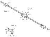
FIG. 1 is a perspective view of one embodiment of a LED lighting unit system according to the invention; -
FIG. 2 is a side view of a lighting unit shown inFIG. 1 ; -
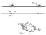
FIG. 3 is a bottom view of the lighting system shown inFIG. 1 with the housing and sealant removed; -
FIG 4 is a side view of the lighting system shown inFIG. 1 with the housing and sealant removed -
FIG. 5 is an exploded top view of one embodiment of a lighting unit inFIG. 1 ; -
FIG. 6 is an exploded bottom view of one embodiment of a lighting unit inFIG. 1 ; -
FIG. 7 is a perspective view of another embodiment of a lighting unit according to the invention before the sealant is applied; -
FIG. 8 is a perspective view of an embodiment of a lighting unit according to the invention after the sealant is applied; -
FIG. 9 is a bottom view of the lighting unit shown inFIG. 8 ; -
FIG. 10a is a perspective view of another embodiment of a lighting unit according to the invention; -
FIG. 10b is a perspective view of the lighting unit shown inFIG. 10a ; -
FIG. 10c is a perspective view of the lighting unit shown inFIG. 10a ; -
FIG. 11 is a perspective view of another embodiment of a lighting unit according to the invention; -
FIG. 12a is a perspective view of another embodiment of a lighting unit according to the invention; -
FIG. 12b is a side view of the lighting unit shown inFIG. 12a ; -
FIG. 13a is a side view of another embodiment of a lighting unit according to the invention; -
FIG. 13b is a side view of another embodiment of a lighting unit according to the invention; -
FIG. 14a is a perspective view of another embodiment of a lighting system according to the invention; -
FIG. 14b is a perspective view of the lighting system shown inFIG. 14a . - The present invention provides a lighting system that can be used in many different applications such as structural lighting, display lighting and ingress/egress lighting, but is particularly applicable to channel letter lighting. The systems according to the present invention provide lighting units that can be interconnected in a chain by electrical conductors so that an electrical signal applied to the input end of the conductors spreads to the lighting units, causing them to emit light. The lighting units can also be powered independently from other lighting units. According to the invention, the lighting units can be placed in a plastic housing; while in other embodiments of the invention the lighting units do not comprise a housing. The side of the lighting unit which can be mounted on a surface will be referred to as the bottom 50 of the lighting unit (shown in
Fig. 1 ). The surface opposite the bottom will be referred to as the top 52. The LEDs are placed in the housing in such a manner that they are on the top of the lighting unit, but angled away from the top surface such that they are no longer parallel to the top surface and can emit at least a portion of their light to the sides of the lighting unit. The plastic housing of the lighting unit is then filled with a sealant, which allows for the lighting units to be customized to meet the particular application. For example, in channel letter applications there may be instances where weatherproofing or additional ruggedness may be desired, and the present invention allows for the sealing or additional ruggedness to be altered, by the use of different housing or filler materials, meeting these different needs. - These embodiments not only allow for the sealing of units to protect them from contaminants, but also allow for both the ability to style the face of the units, since a molded housing is used for the face. Also the units have an added rigidity or ruggedness provided because both a housing and a sealant are utilized.
- In other embodiments of the lighting unit, the light emitting elements of the lighting unit are arranged on an angled surface, such that the angled surface can be adjusted to a desired angle. The lighting unit comprises at least one angled surface with at least one light emitting element on the at least one angled surface. The lighting unit can further comprise a plurality of angled surfaces wherein each angled surface comprises one or more light emitting elements. These lighting units can be customized to adjust and/or alter the emitted light distribution by adjusting the angle of the angled surface so as to meet a particular lighting solution.
- The invention is described herein with reference to certain embodiments but it is understood that the invention can be embodied in many different forms and should not be construed as limited to the embodiments set forth herein. In particular, the invention is described with reference to certain embodiments where the lighting units or lighting unit sections are placed within a molded housing and filled with a sealant, but in other embodiments this process can be modified. In these embodiments, the PCB and lighting elements can be placed in the housing using different methods. In addition, the lighting units may be filled and sealed using a variety of materials. However, in other embodiments, the lighting units are not within or covered by a housing. The invention can also be used with different types of lighting units used in different applications beyond channel letter lighting, and although the invention is described herein with reference to light emitting diodes (LED or LEDs) other light sources can be used.
- It is also understood that when an element such as a layer, region or substrate is referred to as being "on" another element, it can be directly on the other element or intervening elements may also be present. Furthermore, relative terms such as "inner", "outer", "upper", "above", "lower", "beneath", and "below", and similar terms, may be used herein to describe a relationship of one layer or another region. It is understood that these terms are intended to encompass different orientations of the device in addition to the orientation depicted in the figures.
- Although the terms first, second, etc. may be used herein to describe various elements, components, regions, layers and/or sections, these elements, components, regions, layers and/or sections should not be limited by these terms. These terms are only used to distinguish one element, component, region, layer or section from another region, layer or section. Thus, a first element, component, region, layer or section discussed below could be termed a second element, component, region, layer or section without departing from the teachings of the present invention.
- Embodiments of the invention are described herein with reference to illustrations that are schematic illustrations of embodiments of the invention. As such, the actual thickness of the layers and features can be different, and variations from the shapes of the illustrations as a result, for example, of manufacturing techniques and/or tolerances are expected. Embodiments of the invention should not be construed as limited to the particular shapes of the regions illustrated herein but are to include deviations in shapes that result, for example, from manufacturing. A region illustrated or described as square or rectangular will typically have rounded or curved features due to normal manufacturing tolerances. Thus, the regions illustrated in the figures are schematic in nature and their shapes are not intended to illustrate the precise shape of a feature of a device and are not intended to limit the scope of the invention.
-
FIGs. 1 and 2 show one embodiment of alighting system 10 according to the invention that comprises a number oflighting units 12 daisy-chained together by first and secondelectrical conductors lighting units 12 has a number oflight emitting elements unit 12 in response to an electrical signal. The lighting units may have any number oflight emitting elements Fig. 1 . Theelectrical conductors lighting units 12 and an electrical signal applied to theconductors lighting system 10 is conducted to each of thelighting units 12 so that thelight emitting elements lighting units 12 simultaneously emit light. Thelighting units 12 are particularly adapted to being mounted in channel letters, each of which has a transparent or translucent cover. With a translucent cover, when thelight emitting elements - In the figures the same reference numbers will be used herein for the same or similar features with the understanding that the description above applies to this embodiment, as well as the embodiments described below.
-
FIGs. 3 through 9 show thelighting system 10 inFIGs. 1 through 2 in more detail, with thelighting units 12 andconductors lighting units 12 comprises a printed circuit board (PCB) 22 mounted within alighting unit housing 24. ThisPCB 22 can be made of flexible material, rigid material, or any other suitable PCB material. In embodiments where the PCB is made of a flexible material, the LEDs orlighting emitting elements tabs 60 of thePCB 22. In embodiments where thePCB 22 is made of a rigid material, additional wiring may be required from the tabs to the remainder of thePCB 22. Also, in embodiments where thePCB 22 is made of a rigid material, thetabs 60 are arranged such that they may be bent to accommodate the angled shaped plate or insert 62 (also called a housing plate). Thetabs 60 may also be separate portions connected by suitable connection methods and wiring or soldering. As shown inFIG. 5 , thehousing 24 comprises atop housing portion 28 that thePCB 22 can be mounted into. Thetop housing portion 28 can be made of many conductive, semi-conductive and non-conductive materials, with a preferred material being plastic and can be made using many known processes such as by extrusion or injection molding. Thehousing 24 also comprises a shapedplate 62. The shapedplate 62 is inserted in thetop housing portion 28 after thePCB 22 and it functions to force thetabs 60 of thePCB 22 up and through the opening in thetop housing portion 28. Thetabs 60 andlighting emitting elements top housing portion 28 and supported byplate 62. - The
PCB 22 has first, second and thirdlight emitting elements FIGs. 3, 4 ,5 ) mounted to one side on thetabs 60, andconductors conductors PCB 22 aslight emitting elements PCB 22. Theconductors conductors lighting units 12. ThePCB 22 also comprises conductive traces (not shown) to conduct electrical signals from theconductors light emitting elements second conductors light emitting elements light emitting elements - The
light emitting elements elements PCB 22, although they can also be mounted in other locations. In other embodiments thelighting units 12 can comprise more or less than three light emitting elements, such as four, six, and eight or more, that can be mounted in many different locations. Thelight emitting elements light emitting elements light emitting elements output 150 lumens per watt. In some embodiments, light elements may not have a lens, have lenses built in, or they may be added later. - The
PCB 22 can be any conventional type made from any conventional material, with apreferred PCB 22 being a flexible type PCB. Different types of flexible boards can be used such as a board comprised of alternating layers of polyimide film and copper. By being a flexible material,tabs 60 may remain connected to thePCB 22 while capable of flexing in thedirection plate 62 forces thetabs 60. Heat from the light emitting elements conducts into thePCB 22 so that thePCB 22 helps draw away heat from thelight emitting elements PCB 22 then provides a larger surface area that allows the heat to dissipate into the surrounding ambient. This can help keep thelight emitting elements light emitting elements light emitting elements - As shown in
FIG. 8 , thelight emitting elements housing plate 62 forcing thetabs 60 on thePCB 22 out of thetop housing portion 28 and holding thesetabs 60 at a desired angle, shown inFIGs. 5 ,6 , and7 . A thermal hotmelt or sealant is later added to keep thesetabs 60 in place (described below). The light emitting elements are angled and arranged to disperse light evenly in a channel letter lighting unit. Channel letter lighting units have a variety of depths but they largely fall into the 2-5 inch range. Channel letter lighting units which will use LED lighting have a target depth of 2 inches. - The light emitting elements in the application are angled and positioned such that their light emissions overlap over the top of the
lighting unit 12 to create an even light dispersion. The light emitting elements are angled by anglingtabs 60 andtabs 60 are angled by the shapedplate 62. The angle of thetabs 60 directly impacts the angle of the light emitting elements. The light emitting elements generally have a higher output at the center of the light emitting element, but lower output to the sides of each light emitting element. When the light emitting elements are angled, the center and highest intensity output of each light emitting element is angled off center from the lighting unit itself. This direction of light output travels the furthest distance to the surface of the channel letter lighting unit to illuminate the channel letter lighting unit. Therefore providing a higher intensity output at these angles can provide more even light dispersion. The light dispersed directly over thelighting unit 12, is light dispersed at an angle for each of thelight emitting elements lighting unit 12. Further, to accommodate for the lower intensity of light being emitting from thelight elements light elements - In one embodiment using three light emitting elements, the light emitting elements would be angled at 60-75 degrees to provide this even light dispersion. In another embodiment, the light emitting elements would be angles at 45-85 degrees. In yet other embodiments other angle placements of the lighting emitting elements may be used. Preferably, the light emitting elements will not be placed at either 0 degree or 90 degree angles. The
lighting unit 12 may have any number of light emitting elements and the number of light emitting elements and their distance from one another determines exemplary angles the light emitting elements should face for optimal channel letter lighting. For example, if the light emitting elements are further apart, a more decreased angle is desired. However, if the light emitting elements are closer together a steeper angle would be desired. Furthermore, an additional, possibly weaker or brighter, light emitting element may be placed on the surface between the other lighting emitting elements, on top of the dome created byhousing plate 62, to aid in the creation of an even light dispersion. Additionally, the light emitting elements may include optics or lenses over said light elements. - Lighting units according to the invention can also comprise other elements, with one embodiment comprising heat sinks to dissipate heat from the light emitting elements. Another embodiment may comprise constant current devices (not shown) that can be mounted on the PCB using conventional methods. This allows each of the units to have substantially the same current driving its
light emitting elements units 12 emits substantially the same amount of light. Thelight emitting elements system 10 can experience light loss as the power signal passes down theconductors units 12. This can ultimately result in a channel letter exhibiting different brightness across its cover or by different channel letters in a sign having different brightness. By driving each of thelight emitting elements units 12 with the same current, the light emitting elements along the conductor will have the same brightness. Many different constant current devices 30 can be used, with a suitable device being an LM317M 3-Terminal Adjustable Regulator provided by Texas Instruments, National Semiconductor, and Fairchild Semiconductor. - In one embodiment, a
PCB 22 withlight emitting elements conductors Figs. 5 ,6 and7 ), followed byhousing plate 62. Next thecavities 34 left within the top housing portion around theplate 62,light emitting elements PCB 22 are filled with a sealant, which bonds to thehousing 28, PCB, and any other component the sealant contacts within the cavity (shown inFIG. 8 ). The sealant may be filled into the cavities from theside ports 32 of thetop housing portion 28 and then allowed to cure fully. It must be ensured that there are no voids or air cavities and no sealant material is deposited on the light emitter or light emitter lenses. In order to cover the areas of thePCB 22 which are exposed outside of thetop housing portion 28, aroundlighting emitting elements lighting emitting elements lighting emitting elements lighting emitting elements PCB 22 around thelight emitting elements light emitting elements Fig. 7 shows the lighting unit before the sealant is added andFig. 8 shows the lighting unit after thesealant 36 has been added. In some embodiments, this sealant may be a thermoplastic hotmelt which allows for sealing of the lighting unit from contaminants. For example, an embodiment of this lighting unit using a thermoplastic hotmelt as a filler and sealant could receive a large range of ingress protection ratings such as IP00 to IP68 or any other available rating. Some embodiments may have ingress protection ratings which are IP61 to IP68. Other embodiments may have a rating of IP68. When reading ingress protection ratings, the first digit indicates the level of protection that the enclosure provides against access to hazardous parts and the ingress of solid foreign objects. The second digit indicates the level of protection of the equipment inside the enclosure against harmful ingress of water. Generally the higher the number the better the protection. One suitable thermoplastic hotmelt is Macromelt © manufactured by Henkel AG & Co. - Bonding of the
sealant 36 to components within thetop housing portion 28 and filling of thecavities 34, also reduces strain on connections within the lighting unit such as strain on theemitter conductors - Conventional lighting units utilizing only a plastic housing provides rigidity but not a weatherproof seal. Conventional lighting units utilizing only a sealant or thermoplastic hotmelt provides weatherproofing but does not produce as rigid of a product and the product face cannot be styled as that of one with a plastic housing. Utilizing both a
top housing portion 28 and asealant 36 such as macromelt can provide additional rigidity, weatherproofing, and a product face which can be stylized. This provides a product robust for installation and with a finished appearance. - Each
lighting unit 12 can be mounted within a channel letter by many different methods such as by glue, clamp, bolt, weld, etc.Lighting unit 12 can be provided with double sided tape on itsbottom surface 50 for mounting, as shown inFIG. 9 . Many different doublesided tapes 64 can be used, with an exemplary tape being a commercially available double sided foam tape provided by 3M Corporation. Thelighting unit 12 can also be provided with an alternative mounting method that can be used alone or in conjunction with the double sided tape. Thetop housing portion 28 includes ahousing mounting hole 42 through which a screw, nail or rivet can pass to mount the housing 24 (shown inFIG. 8 ). ThePCB 22 also comprises aPCB mounting hole 44 in alignment with thehousing mounting hole 42.Sealant 36 is applied in a manner, such as by blocking the area from sealant or any other suitable manner, which does not fill mountinghole 42 so that mountinghole 42 extends through the lighting unit. In one embodiment according to the present invention a screw can pass through thePCB mounting hole 44 and into the top housingportion mounting hole 42. A screwdriver can then pass through thePCB mounting hole 44 to turn the screw into the channel letter, through thetop housing portion 28 mountinghole 42. - In another embodiment of the invention, as shown in
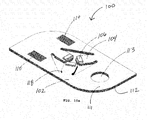
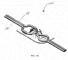
FIGs. 10a-10c , alighting unit 100 comprises aPCB 102 having at least onetab 104 and at least onelight emitting element 106 on the at least onetab 104. The at least onetab 104 is adapted to be angled in relation to thePCB 102 such that the at least onelight emitting element 106 is on anangled surface 108. Thelighting unit 100 further compriseselectrical conductors light emitting element 106 to cause the at least onelight emitting element 106 to emit light substantially away from thePCB 102. - The
PCB 102 comprises a top surface 111, abottom surface 112 and aslot 113, wherein the at least onelight emitting element 106 is on the top surface 111 of thePCB 102. ThePCB 102 further comprisescontact pads 110 on the top surface 111 that are arranged to receive theelectrical conductors electrical conductors respective contact pad 110 so that theelectrical conductors light emitting element 106. In some embodiments, theelectrical conductors respective contact pad 110. However, in other embodiments, theelectrical conductors contact pad 110 by using an Insulation Piercing Connector (IPC) or an Insulation Displacement Connector (IDC). ThePCB 102 also comprises trace elements (not shown) between thecontact pads 110 and the at least onelight emitting element 106 to allow the electrical signal to be provided to the at least onelight emitting element 106. - The
PCB 102 can be made of many different materials, such as but not limited to, flexible materials, rigid materials, or any other suitable PCB material. Thetabs 104 are arranged such that they are flexible and can be bent to form theangled surface 108 without causing damage to thePCB 102, and are able to retain the shape of theangled surface 108. As shown inFIGs. 10a-10c , thetabs 104 are bent about a joint 118, wherein the joint 118 connects thetabs 104 to thePCB 102. In other embodiments, the angle of theangled surface 108 may be maintained by placing a supportive structure (not shown) adjacent or proximate thetab 104 in order to ensure that the angle of theangled surface 108 is not changed due to gravity and/or other external influences. In the embodiment shown inFIGs. 10a-10c , thePCB 102 comprises threetabs 104 in a triangular-like configuration, but the configuration of thetabs 104 is not intended to be limited to a triangular configuration. In other embodiments, thePCB 102 can comprise one ormore tabs 104 and thesetabs 104 can be configured in many different configurations, such as but not limited to circular, linear, square or any other configuration. - In some embodiments, the
lighting unit 100 can have more than onelight emitting element 106. For example, as shown inFIGs. 10a-10c , eachtab 104 can have onelight emitting element 106. In other embodiments, eachtab 104 can have one or morelight emitting elements 106. In yet other embodiments, thetabs 104 can have an equal amount oflight emitting elements 106 on eachrespective tab 104. While in other embodiments, thetabs 104 can have a different amount oflight emitting elements 106 on eachrespective tab 104. Thetabs 104 may also be separate portions connected to thePCB 102 at the joint 118 by suitable connection methods and wiring or soldering. - The at least one
light emitting element 106 can be any device that emits light in response to an electrical signal, such as incandescent lights, lasers, laser diodes, fluorescent light, neon lights or light emitting diodes (LED). For embodiments comprising more than onelight emitting element 106, thelight emitting elements 106 can emit different colors of different intensities, with a suitable LED comprising commercially available LEDs. In some embodiments, as shown inFIG. 11 , thelighting unit 100 can comprise anoptical element 150 on thePCB 102 and proximate the at least onelight emitting element 106, such that the light emitted from the at least onelight emitting element 106 is altered and/or dispersed due to the features of the optical element. In some embodiments, theoptical element 150 is over and covering the at least onelight emitting element 106, while in other embodiments, theoptical element 150 surrounds the at least onelight emitting element 106. Theoptical element 150 can be a reflector to reflect light in a certain direction, a lens to concentrate or alter the emitted light, or a diffuser to diffuse the light emitted from the at least onelight emitting element 106, or a combination thereof. Theoptical element 150 can be mounted on thePCB 102 using various different methods, such as but not limited to being glued onto thePCB 102, mechanically fastened to thePCB 102, overmolded onto thePCB 102, or slidably mounted onto thePCB 102. This is a non-exhaustive list of examples of how the optical element can be mounted on thePCB 102, and are not intended to be limited to the examples disclosed herein. Theoptical element 150 can be mounted on thePCB 102 when thelighting unit 100 is fabricated or it can be mounted at any time after fabrication of thelighting unit 100. - As discussed above, the
PCB 102 can be any conventional type made from any conventional material, such as aflexible type PCB 102. Different types of flexible boards can be used such as a board comprised of alternating layers of polyimide film and copper. By being a flexible material, the at least onetab 104 may remain connected to thePCB 102 while being capable of flexing in a direction substantially orthogonal to thePCB 102. ThePCB 102 is further configured such that heat from the at least onelight emitting element 106 conducts into thePCB 102 so that thePCB 102 helps draw away heat from the at least onelight emitting element 106. ThePCB 102 provides a larger surface area that allows the heat to dissipate into the surrounding ambient. This can help keep the at least onelight emitting element 106 cooler, which can allow it to operate under a higher current so that it can emit a higher luminous flux. Also, the at least onelight emitting element 106 may last longer if operating at a cooler temperature. In embodiments of the lighting unit comprising aPCB 102 constructed of alternating layers of polyimide film and copper, the copper layers would allow for heat dissipation. Thermal vias, which connect the copper planes together, may be added proximate the at least onelight emitting element 106 to allow for better, more efficient heat transfer. - The at least one
light emitting element 106, as shown inFIGs. 10b and10c , is angled such that the at least onelight emitting element 106 is not facing a direction perpendicular to thePCB 102. However, in some embodiments, the at least onelight emitting element 106 can face a direction perpendicular to thePCB 102, such that theangled surface 108 is set at an angle of 0 degrees with respect to thePCB 102. Theangled surface 108 can be set at any time before or after installation of thelighting unit 100. The at least onelight emitting element 106 is angled and arranged to emit light evenly, and can be installed in a channel letter. Channel letters have a variety of depths, with a typical depth within the range of 2-5 inches. In embodiments having more than onelight emitting element 106, thelight emitting elements 106 are angled such that the emitted light from each light emittingelement 106 overlaps over the top of thelighting unit 100 to create an even light distribution. In other embodiments, thelight emitting elements 106 can be angled such that the emitted light does not overlap. The angle of theangled surface 108 determines the overall light distribution of thelighting unit 100. In some instances different applications would require different lighting needs and having angledsurfaces 108 that are set at different angles that will provide a desired light distribution that could not be provided if all the angled surfaces were set at the same angle for a given channel letter housing, for example, a non-standard shaped channel letters, such as but not limited to a cloud box, or when space limitations do not allow the lighting unit to be mounted in a location to allow even light emission. - The angle of the at least one
tab 104 can be set at various different angles to form theangled surface 108, based on the desired light distribution for a lighting application. For example, in some embodiments the at least onetab 104 can be set at an angle within the range of 60-75 degrees to provide an even light distribution. While in other embodiments, the at least onetab 104 can be set at an angle within the range of 45-85 degrees. In yet other embodiments, the angle of theangled surface 108 can be within the range of 0-90 degrees. As stated above, embodiments comprising more than onetab 104 can have the angled surface set at different settings and can be within the ranges disclosed herein. Thelighting unit 100 may have any number oflight emitting elements 106 and the number oflight emitting elements 106 and their distance from one another determines the angles of theangled surfaces 108 upon which thelight emitting elements 106 should face for optimal channel letter lighting. For example if thelight emitting elements 106 are further apart, theangled surface 108 should be set at a more decreased angle is desired, whereas, if thelight emitting elements 108 are closer together theangled surface 108 should be set at a steeper angle. - The
lighting unit 100 can also comprise other elements, with one embodiment comprising heat sinks to dissipate heat from thelight emitting elements 106. Other embodiments may comprise constant current devices (not shown) that can be mounted on thePCB 102 using conventional methods. This allows thelighting unit 100 to have substantially the same current driving thelight emitting elements 106 such that each of thelight emitting elements 106 emits substantially the same amount of light. Thelight emitting elements 106 and constant current device can be interconnected by conductive traces on thePCB 102 using conventional methods. Without a constant current device, thelighting unit 100 can experience light loss as the electrical signal passes through theconductors light emitting elements 106. This can ultimately result in thelighting unit 100 exhibiting different brightness across its light emission pattern. By driving each of thelight emitting elements 106 in each of thelighting units 100 with the same current, thelight emitting elements 106 within thelighting unit 100 will emit light at substantially the same brightness. In yet other embodiments, thelighting unit 100 can further comprise a transparent coating that covers all the components of thelighting unit 100. The transparent coating can be a conformal coating that provides a protective coating over the elements on the front and/or back surface of thePCB 102. The transparent coating can be made of a transparent resin, epoxy or the like. The transparent coating can be made of many different materials and is not intended to be limited to the embodiments presented herein. - The
lighting unit 100 is particularly adapted to being mounted in channel letters which can have a transparent or translucent cover, to form alighting system 140. Thelighting system 140 comprises at least onelighting unit 100 mounted in a channel letter (not shown). Thelighting system 140 can also comprise a plurality oflighting units 100 connected in a daisy-chain configuration using theelectrical conductors slot 113 of thelighting unit 100 is adapted to receive a mounting device such as, but not limited to, a screw, nail, rivet or the like so as to extend through theslot 113 and mount thelighting unit 100 to the channel letter. Thelighting unit 100 can be mounted in a variety of ways and is not intended to be limited to the examples disclosed herein. In other embodiments, thelighting unit 100 can be mounted onto a carrier or bracket (not shown) instead of being mounted onto a surface of the channel letter. The carrier or bracket can also be used in embodiments wherein the lighting unit is configured to be a double-sided lighting unit (discussed below). The carrier allows the double-sided lighting unit to be mounted away from the surfaces of the channel letter to allow the double-sided lighting unit to emit light towards both the front and back of the channel letter. For channel letters with a translucent cover, when the at least onelight emitting element 106 is illuminated in the channel letter the light can be diffused by the features on or adjacent thelight emitting element 106 or the translucent cover of the channel letter, in order to give the appearance that the channel letter has a continuous light source. - The spacing between
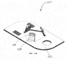
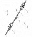
adjacent lighting units 100 within thelighting system 140 can be altered to modify the density oflighting units 100 or light emittingelements 106 in a chain oflighting units 100. Altering the density of lighting units can alter the overall light distribution pattern of thelighting system 140. The density can be decreased by increasing the length of theelectrical conductors adjacent lighting units 100. As shown inFIG. 14a , thelighting system 140 comprises a plurality oflighting units 100 in a daisy-chain configuration, wherein theelectrical conductors lighting unit 100 to anadjacent lighting unit 100. Theelectrical conductors adjacent lighting units 100 are arranged in a coiled or serpentine manner to provide an additional amount ofelectrical conductors electrical conductors lighting unit 100 is mounted. The additional amount ofelectrical conductors clamping device 142, such as but not limited to a clip, clamp, bracket, rubber band, or the like. In other embodiments, theclamping device 142 can be overmolded onto theelectrical conductors - To increase the length between
adjacent lighting units 100 of thelighting system 140, a pulling force is applied that is sufficient to overcome the holding force between theelectrical conductors clamping device 142. This results in the additional section being released from theclamping device 142 thereby increasing the length betweenadjacent lighting units 100, as shown inFIG. 14b . An advantage of the invention is that extending the length of the electrical conductors betweenadjacent lighting units 100 provides flexibility in adjusting the lengths between adjacent units as well as flexibility in the lighting unit density. Another advantage of the invention is that the additional amount ofelectrical conductors adjacent lighting units 100, or can be configured to allow another device to be electrically connected to thelighting units 100, such as but not limited to an external power supply or controller. - The embodiments of the
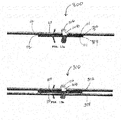
lighting unit 100 shown inFIGs. 10a-11 disclose a singled-sided lighting unit. However, in other embodiments of the invention, alighting unit 200 is arranged to be a double-sided lighting unit. Thelighting unit 200, shown inFIGs. 12a and 12b , is similarly configured to thelighting unit 100, but is further arranged such that at least onetab 106 can be bent in a direction that is substantially orthogonal to thebottom surface 112 of thePCB 102. - The
lighting unit 200 comprises aPCB 102, at least onetab 104, and at least onelight emitting element 106 on the at least onetab 104. ThePCB 102 further comprises a top surface 111, abottom surface 112 and aslot 113, wherein at least onelight emitting element 106 is on the top surface 111 and thebottom surface 112. The at least onetab 104 is adapted to be angled in relation to either of a top orbottom surface 111, 112 of thePCB 102 such that the at least onelight emitting element 106 is on anangled surface 108. As shown inFIGs. 12a and 12b , the at least onetab 104 is adapted to be bent to form anangled surface 108 with respect to thebottom surface 112 of thePCB 102, while theother tabs 104 are adapted to be bent to form anangled surface 108 with respect to the top surface 111 of thePCB 102. Thetabs 104 are adapted to be bent in a similar fashion and within a similar range as the tabs oflighting unit 100, discussed above. Bending thetabs 104 with respect to the top andbottom surfaces 111, 112 of thePCB 102 allows thelight emitting elements 106 to emit light substantially away from both the top andbottom surfaces 111, 112 of thePCB 102, thereby forming the double-sided lighting unit 200. An advantage of the invention is that thelighting unit 200 can be mounted in channel letters that have a transparent or translucent cover on a front and back surface, such that the light emitted from thelight emitting elements 106 illuminates both the front and back surface of the channel letter. Furthermore, the angle of the at least onetab 104 can be adjusted at any time before or after installation which allows the light distribution to be adjusted to accommodate for any lighting application. Thelighting unit 200 allows for only one lighting unit to be used to provide illumination to the front and back surfaces of the channel letter, which can be advantageous for lighting applications where space is limited and/or cannot allow for multiple lighting units to be used. -
FIGs. 12a and 12b show that only onetab 104 is bent to form anangled surface 108 with respect to thebottom surface 112 of thePCB 102. However, in other embodiments, more than onetab 104 can be bent to form anangled surface 108 with respectbottom surface 112. In yet other embodiments, thelighting unit 200 can be configured such that a plurality oftabs 104 are bent to form anangled surface 108 with respect to the top surface 111 and a plurality oftabs 104 are bent to form anangled surface 108 with respect to thebottom surface 112 of thePCB 102. Thelighting unit 200 further compriseselectrical conductors light emitting element 106 to cause the at least onelight emitting element 106 to emit light in response to the electrical signal. Thelighting unit 200 can also comprise anoptical element 150, similarly configured as in thelighting unit 100. -
FIG. 13a discloses another embodiment of the invention wherein alighting unit 300 is also configured to be a double-sided lighting unit. Thelighting unit 300 is comprised of afirst PCB 302 and asecond PCB 304 arranged in a back-to-back configuration, wherein each of the first andsecond PCBs tab 104 arranged to be bent to form anangled surface 108 with respect to the top surface 111 of itsrespective PCB second PCBs lighting unit 300 are similarly configured as thePCB 102 oflighting unit 100. Thelighting unit 300 further comprises acontact pad 110 which is arranged to receive theelectrical conductors second PCBs lighting unit 300 are electrically connected such that the electrical signal provided by theelectrical conductors light emitting elements 106 on both of the first andsecond PCBs lighting unit 300 can also comprise anoptical element 150 on the first and/orsecond PCB lighting unit 100. - In other embodiments, as shown in
FIG. 13b , alighting unit 310 is configured similarly as thelighting unit 300, but the first andsecond PCBs lighting unit 310 are electrically isolated from each other. The first andsecond PCBs electrical conductors PCBs light emitting elements 106 of therespective PCBs light emitting elements 106 to adjust and/or alter the overall light distribution or desired lighting effect of thelighting unit 310. For example, the at least onelight emitting element 106 on thefirst PCB 302 can be arranged to emit at a higher, lower or similar luminous flux than the at least onelight emitting element 106 on thesecond PCB 304, and vice versa. Thelighting unit 310 can also comprise anoptical element 150 on the first and/orsecond PCB lighting unit 100. - At least one distinction between the
lighting units lighting unit 12, discussed above and shown inFIGs. 1-9 , is that thelighting units PCBs lighting unit PCB 22 of thelighting unit 12 is mounted within thehousing 24. At least one advantage of the invention is that the at least onetab 104 of thelighting units tab 104 can be set and or adjusted at any time. For instance, the angle of the at least onetab 104 can be set at any time prior to or after thelighting units tab 104 can be adjusted to a different angle in order to modify or alter the lighting characteristics of thelighting unit lighting units lighting unit 12 is thatlighting units lighting unit 12 is a single-sided lighting unit. Thelighting units lighting units electrical conductors lighting units clamping device 142 as discussed above. - Although the invention has been described in considerable detail with reference to certain embodiments thereof, other versions are possible. Lighting units according to the invention can be used for many different applications beyond channel letters. A separate power supply can be used for each channel letter or multiple letters can be powered by a single power supply. In other embodiments, a variable power supply can be used to control the intensity of the light emitting elements. The lighting unit can be many different sizes and can be used in many different applications beyond channel letters. The PCB can have different numbers of LEDs and can have different electronic components arranged in different ways. The conductors can be different lengths and instead of running uninterrupted between the units, the conductors can have connectors. This would allow the units to be supplied separately and then connected together when installed. Therefore, the spirit and scope of the invention and should not be limited to the preferred versions described above.
Claims (15)
- A lighting unit, comprising:a printed circuit board (PCB) comprising a front surface, a back surface and at least one tab;at least one light emitting element on said PCB;said at least one tab adapted to be bent in a direction away from said PCB to form an angled surface with respect to the PCB, wherein said at least one light emitting element is on said angled surface; andconductors electrically connected with said PCB to provide an electrical signal to said at least one light emitting element, such that said at least one light emitting element emits light substantially away from said PCB.
- The lighting unit of claim 1, wherein said PCB comprises a metal core PCB arranged to conduct heat away from said at least one light emitting element.
- The lighting unit of claim 1, wherein said PCB comprises alternating layers of polymide film and copper.
- The lighting unit of claim 3, wherein said PCB further comprises vias arranged proximate said at least one light emitting element to assist in heat dissipation.
- The lighting unit of claim 1, wherein said PCB is capable of conducting and dissipating heat from said at least one light emitting element.
- The lighting unit of claim 1, wherein said PCB comprises a plurality of tabs and a plurality of light emitting elements, wherein each of said plurality of tabs comprises at least one of said plurality of light emitting elements.
- The lighting unit of claim 1, wherein said at least one tab is configured to be bent about a joint in order to form said angled surface, said joint disposed between said at least one tab and said PCB.
- The lighting unit of claim 1, wherein said at least one tab is adapted to be set at an angle within the range of 0-90 degrees with respect to said PCB.
- The lighting unit of claim 6, wherein said plurality of tabs are bent such that said angled surfaces are angled within the range of 0-90 degrees with respect to said PCB.
- The lighting unit of claim 9, wherein each of said angled surfaces are set at the same angle with respect to said PCB.
- The lighting unit of claim 9, wherein at least one of said angled surfaces is set at a different angle with respect to said PCB and the other of said angled surfaces.
- The lighting unit of claim 1, wherein said angled surface is adapted to be adjusted at any time prior to or after installation of the lighting unit.
- The lighting unit of claim 1, said PCB further comprising a slot adapted to receive a mounting device to allow said lighting unit to be mounted onto a surface or other structure.
- The lighting unit of claim 1, further comprising an optical element on said PCB and proximate said at least one light emitting element to alter the light emitted from the at least one light emitting element.
- The lighting unit of claim 14, wherein said optical element comprises at least one of a lens, diffuser, reflector, or a combination thereof.
Applications Claiming Priority (1)
| Application Number | Priority Date | Filing Date | Title |
|---|---|---|---|
| US13/653,282 US9170000B2 (en) | 2008-12-12 | 2012-10-16 | Angled emitter channel letter lighting |
Publications (3)
| Publication Number | Publication Date |
|---|---|
| EP2722589A2 true EP2722589A2 (en) | 2014-04-23 |
| EP2722589A3 EP2722589A3 (en) | 2017-11-22 |
| EP2722589B1 EP2722589B1 (en) | 2020-02-26 |
Family
ID=49356308
Family Applications (1)
| Application Number | Title | Priority Date | Filing Date |
|---|---|---|---|
| EP13188775.4A Active EP2722589B1 (en) | 2012-10-16 | 2013-10-15 | Angled emitter channel letter lighting |
Country Status (2)
| Country | Link |
|---|---|
| EP (1) | EP2722589B1 (en) |
| CN (2) | CN112128643A (en) |
Cited By (2)
| Publication number | Priority date | Publication date | Assignee | Title |
|---|---|---|---|---|
| EP3012513A1 (en) * | 2014-10-23 | 2016-04-27 | Edison Opto Corporation | Led light core structure |
| EP3399230A1 (en) * | 2017-04-26 | 2018-11-07 | OSRAM GmbH | Lighting module, method for manufacturing the same and luminous signage device comprising such lighting module |
Families Citing this family (1)
| Publication number | Priority date | Publication date | Assignee | Title |
|---|---|---|---|---|
| DE102015206805B4 (en) * | 2015-04-15 | 2022-10-27 | Ledvance Gmbh | Lamps with LEDs |
Citations (4)
| Publication number | Priority date | Publication date | Assignee | Title |
|---|---|---|---|---|
| US5697175A (en) | 1993-10-12 | 1997-12-16 | Spectralight, Inc. | Low power drain illuminated sign |
| US6042248A (en) | 1997-10-15 | 2000-03-28 | Lektron Industrial Supply, Inc. | LED assembly for illuminated signs |
| US6932495B2 (en) | 2001-10-01 | 2005-08-23 | Sloanled, Inc. | Channel letter lighting using light emitting diodes |
| US7241031B2 (en) | 2004-04-14 | 2007-07-10 | Sloanled, Inc. | Channel letter lighting system using high output white light emitting diodes |
Family Cites Families (10)
| Publication number | Priority date | Publication date | Assignee | Title |
|---|---|---|---|---|
| US7086756B2 (en) * | 2004-03-18 | 2006-08-08 | Lighting Science Group Corporation | Lighting element using electronically activated light emitting elements and method of making same |
| JP2007073723A (en) * | 2005-09-07 | 2007-03-22 | Nok Corp | Fitting method for led and fitting structure for led |
| US8465175B2 (en) * | 2005-11-29 | 2013-06-18 | GE Lighting Solutions, LLC | LED lighting assemblies with thermal overmolding |
| FR2908500A1 (en) * | 2006-11-13 | 2008-05-16 | Sphere 01 Sarl | Light device for illuminating or signaling e.g. lane, has envelope covering base that has printed circuit board defining surfaces, where surfaces are engraved in non coplanar planes and integrate point light sources |
| JP2008123931A (en) * | 2006-11-15 | 2008-05-29 | Epson Imaging Devices Corp | Lighting device, electro-optical device, and electronic apparatus |
| TWI352179B (en) * | 2008-11-20 | 2011-11-11 | Everlight Electronics Co Ltd | Light module |
| US8845131B2 (en) * | 2008-12-12 | 2014-09-30 | The Sloan Company, Inc. | Angled light box lighting system |
| US9080745B2 (en) * | 2008-12-12 | 2015-07-14 | The Sloan Company, Inc. | Angled emitter channel letter lighting |
| TWI401788B (en) * | 2008-12-24 | 2013-07-11 | Ind Tech Res Inst | Led packaging module and method |
| JP2012018865A (en) * | 2010-07-09 | 2012-01-26 | Panasonic Corp | Led module and led lamp |
-
2013
- 2013-10-15 EP EP13188775.4A patent/EP2722589B1/en active Active
- 2013-10-16 CN CN202010894669.5A patent/CN112128643A/en active Pending
- 2013-10-16 CN CN201310680094.7A patent/CN103727461A/en active Pending
Patent Citations (4)
| Publication number | Priority date | Publication date | Assignee | Title |
|---|---|---|---|---|
| US5697175A (en) | 1993-10-12 | 1997-12-16 | Spectralight, Inc. | Low power drain illuminated sign |
| US6042248A (en) | 1997-10-15 | 2000-03-28 | Lektron Industrial Supply, Inc. | LED assembly for illuminated signs |
| US6932495B2 (en) | 2001-10-01 | 2005-08-23 | Sloanled, Inc. | Channel letter lighting using light emitting diodes |
| US7241031B2 (en) | 2004-04-14 | 2007-07-10 | Sloanled, Inc. | Channel letter lighting system using high output white light emitting diodes |
Cited By (2)
| Publication number | Priority date | Publication date | Assignee | Title |
|---|---|---|---|---|
| EP3012513A1 (en) * | 2014-10-23 | 2016-04-27 | Edison Opto Corporation | Led light core structure |
| EP3399230A1 (en) * | 2017-04-26 | 2018-11-07 | OSRAM GmbH | Lighting module, method for manufacturing the same and luminous signage device comprising such lighting module |
Also Published As
| Publication number | Publication date |
|---|---|
| CN112128643A (en) | 2020-12-25 |
| CN103727461A (en) | 2014-04-16 |
| EP2722589B1 (en) | 2020-02-26 |
| EP2722589A3 (en) | 2017-11-22 |
Similar Documents
| Publication | Publication Date | Title |
|---|---|---|
| US9170000B2 (en) | Angled emitter channel letter lighting | |
| EP2526335B1 (en) | Angled emitter channel letter lighting | |
| US7241031B2 (en) | Channel letter lighting system using high output white light emitting diodes | |
| US8845131B2 (en) | Angled light box lighting system | |
| US7213941B2 (en) | Flexible perimeter lighting apparatus | |
| US9410665B2 (en) | Flexible ribbon LED module | |
| US9200788B2 (en) | Angled light box lighting system | |
| US20110194284A1 (en) | Channel letter lighting system using high output white light emitting diodes | |
| US20130077300A1 (en) | Display box lighting module | |
| US20100149811A1 (en) | Channel letter lighting system using high output white light emitting diodes | |
| EP2722589B1 (en) | Angled emitter channel letter lighting | |
| EP3132184B1 (en) | Flexible ribbon led module | |
| US20130188357A1 (en) | Channel letter lighting system using high output white light emitting diodes | |
| WO2014014903A1 (en) | Flexible ribbon led module | |
| EP1751732B1 (en) | Channel letter lighting system using high output white light emitting diodes | |
| EP2976568B1 (en) | Angled light box lighting system | |
| WO2014138464A1 (en) | Channel letter lighting system using high output white light emitting diodes |
Legal Events
| Date | Code | Title | Description |
|---|---|---|---|
| PUAI | Public reference made under article 153(3) epc to a published international application that has entered the european phase |
Free format text: ORIGINAL CODE: 0009012 |
|
| AK | Designated contracting states |
Kind code of ref document: A2 Designated state(s): AL AT BE BG CH CY CZ DE DK EE ES FI FR GB GR HR HU IE IS IT LI LT LU LV MC MK MT NL NO PL PT RO RS SE SI SK SM TR |
|
| AX | Request for extension of the european patent |
Extension state: BA ME |
|
| PUAL | Search report despatched |
Free format text: ORIGINAL CODE: 0009013 |
|
| AK | Designated contracting states |
Kind code of ref document: A3 Designated state(s): AL AT BE BG CH CY CZ DE DK EE ES FI FR GB GR HR HU IE IS IT LI LT LU LV MC MK MT NL NO PL PT RO RS SE SI SK SM TR |
|
| AX | Request for extension of the european patent |
Extension state: BA ME |
|
| RIC1 | Information provided on ipc code assigned before grant |
Ipc: F21S 4/00 20160101ALI20171018BHEP Ipc: F21V 21/08 20060101ALI20171018BHEP Ipc: F21V 31/00 20060101AFI20171018BHEP Ipc: F21V 23/00 20150101ALN20171018BHEP Ipc: H05K 1/02 20060101ALI20171018BHEP |
|
| STAA | Information on the status of an ep patent application or granted ep patent |
Free format text: STATUS: REQUEST FOR EXAMINATION WAS MADE |
|
| 17P | Request for examination filed |
Effective date: 20180522 |
|
| RBV | Designated contracting states (corrected) |
Designated state(s): AL AT BE BG CH CY CZ DE DK EE ES FI FR GB GR HR HU IE IS IT LI LT LU LV MC MK MT NL NO PL PT RO RS SE SI SK SM TR |
|
| GRAP | Despatch of communication of intention to grant a patent |
Free format text: ORIGINAL CODE: EPIDOSNIGR1 |
|
| STAA | Information on the status of an ep patent application or granted ep patent |
Free format text: STATUS: GRANT OF PATENT IS INTENDED |
|
| INTG | Intention to grant announced |
Effective date: 20190912 |
|
| GRAS | Grant fee paid |
Free format text: ORIGINAL CODE: EPIDOSNIGR3 |
|
| GRAA | (expected) grant |
Free format text: ORIGINAL CODE: 0009210 |
|
| STAA | Information on the status of an ep patent application or granted ep patent |
Free format text: STATUS: THE PATENT HAS BEEN GRANTED |
|
| AK | Designated contracting states |
Kind code of ref document: B1 Designated state(s): AL AT BE BG CH CY CZ DE DK EE ES FI FR GB GR HR HU IE IS IT LI LT LU LV MC MK MT NL NO PL PT RO RS SE SI SK SM TR |
|
| REG | Reference to a national code |
Ref country code: GB Ref legal event code: FG4D |
|
| REG | Reference to a national code |
Ref country code: CH Ref legal event code: EP |
|
| REG | Reference to a national code |
Ref country code: AT Ref legal event code: REF Ref document number: 1238074 Country of ref document: AT Kind code of ref document: T Effective date: 20200315 |
|
| REG | Reference to a national code |
Ref country code: IE Ref legal event code: FG4D |
|
| REG | Reference to a national code |
Ref country code: DE Ref legal event code: R096 Ref document number: 602013066190 Country of ref document: DE |
|
| REG | Reference to a national code |
Ref country code: NL Ref legal event code: FP |
|
| PG25 | Lapsed in a contracting state [announced via postgrant information from national office to epo] |
Ref country code: RS Free format text: LAPSE BECAUSE OF FAILURE TO SUBMIT A TRANSLATION OF THE DESCRIPTION OR TO PAY THE FEE WITHIN THE PRESCRIBED TIME-LIMIT Effective date: 20200226 Ref country code: NO Free format text: LAPSE BECAUSE OF FAILURE TO SUBMIT A TRANSLATION OF THE DESCRIPTION OR TO PAY THE FEE WITHIN THE PRESCRIBED TIME-LIMIT Effective date: 20200526 Ref country code: FI Free format text: LAPSE BECAUSE OF FAILURE TO SUBMIT A TRANSLATION OF THE DESCRIPTION OR TO PAY THE FEE WITHIN THE PRESCRIBED TIME-LIMIT Effective date: 20200226 |
|
| REG | Reference to a national code |
Ref country code: LT Ref legal event code: MG4D |
|
| PG25 | Lapsed in a contracting state [announced via postgrant information from national office to epo] |
Ref country code: IS Free format text: LAPSE BECAUSE OF FAILURE TO SUBMIT A TRANSLATION OF THE DESCRIPTION OR TO PAY THE FEE WITHIN THE PRESCRIBED TIME-LIMIT Effective date: 20200626 Ref country code: GR Free format text: LAPSE BECAUSE OF FAILURE TO SUBMIT A TRANSLATION OF THE DESCRIPTION OR TO PAY THE FEE WITHIN THE PRESCRIBED TIME-LIMIT Effective date: 20200527 Ref country code: HR Free format text: LAPSE BECAUSE OF FAILURE TO SUBMIT A TRANSLATION OF THE DESCRIPTION OR TO PAY THE FEE WITHIN THE PRESCRIBED TIME-LIMIT Effective date: 20200226 Ref country code: SE Free format text: LAPSE BECAUSE OF FAILURE TO SUBMIT A TRANSLATION OF THE DESCRIPTION OR TO PAY THE FEE WITHIN THE PRESCRIBED TIME-LIMIT Effective date: 20200226 Ref country code: LV Free format text: LAPSE BECAUSE OF FAILURE TO SUBMIT A TRANSLATION OF THE DESCRIPTION OR TO PAY THE FEE WITHIN THE PRESCRIBED TIME-LIMIT Effective date: 20200226 Ref country code: BG Free format text: LAPSE BECAUSE OF FAILURE TO SUBMIT A TRANSLATION OF THE DESCRIPTION OR TO PAY THE FEE WITHIN THE PRESCRIBED TIME-LIMIT Effective date: 20200526 |
|
| PG25 | Lapsed in a contracting state [announced via postgrant information from national office to epo] |
Ref country code: DK Free format text: LAPSE BECAUSE OF FAILURE TO SUBMIT A TRANSLATION OF THE DESCRIPTION OR TO PAY THE FEE WITHIN THE PRESCRIBED TIME-LIMIT Effective date: 20200226 Ref country code: PT Free format text: LAPSE BECAUSE OF FAILURE TO SUBMIT A TRANSLATION OF THE DESCRIPTION OR TO PAY THE FEE WITHIN THE PRESCRIBED TIME-LIMIT Effective date: 20200719 Ref country code: EE Free format text: LAPSE BECAUSE OF FAILURE TO SUBMIT A TRANSLATION OF THE DESCRIPTION OR TO PAY THE FEE WITHIN THE PRESCRIBED TIME-LIMIT Effective date: 20200226 Ref country code: SM Free format text: LAPSE BECAUSE OF FAILURE TO SUBMIT A TRANSLATION OF THE DESCRIPTION OR TO PAY THE FEE WITHIN THE PRESCRIBED TIME-LIMIT Effective date: 20200226 Ref country code: ES Free format text: LAPSE BECAUSE OF FAILURE TO SUBMIT A TRANSLATION OF THE DESCRIPTION OR TO PAY THE FEE WITHIN THE PRESCRIBED TIME-LIMIT Effective date: 20200226 Ref country code: LT Free format text: LAPSE BECAUSE OF FAILURE TO SUBMIT A TRANSLATION OF THE DESCRIPTION OR TO PAY THE FEE WITHIN THE PRESCRIBED TIME-LIMIT Effective date: 20200226 Ref country code: RO Free format text: LAPSE BECAUSE OF FAILURE TO SUBMIT A TRANSLATION OF THE DESCRIPTION OR TO PAY THE FEE WITHIN THE PRESCRIBED TIME-LIMIT Effective date: 20200226 Ref country code: CZ Free format text: LAPSE BECAUSE OF FAILURE TO SUBMIT A TRANSLATION OF THE DESCRIPTION OR TO PAY THE FEE WITHIN THE PRESCRIBED TIME-LIMIT Effective date: 20200226 Ref country code: SK Free format text: LAPSE BECAUSE OF FAILURE TO SUBMIT A TRANSLATION OF THE DESCRIPTION OR TO PAY THE FEE WITHIN THE PRESCRIBED TIME-LIMIT Effective date: 20200226 |
|
| REG | Reference to a national code |
Ref country code: AT Ref legal event code: MK05 Ref document number: 1238074 Country of ref document: AT Kind code of ref document: T Effective date: 20200226 |
|
| REG | Reference to a national code |
Ref country code: DE Ref legal event code: R097 Ref document number: 602013066190 Country of ref document: DE |
|
| PLBE | No opposition filed within time limit |
Free format text: ORIGINAL CODE: 0009261 |
|
| STAA | Information on the status of an ep patent application or granted ep patent |
Free format text: STATUS: NO OPPOSITION FILED WITHIN TIME LIMIT |
|
| PG25 | Lapsed in a contracting state [announced via postgrant information from national office to epo] |
Ref country code: IT Free format text: LAPSE BECAUSE OF FAILURE TO SUBMIT A TRANSLATION OF THE DESCRIPTION OR TO PAY THE FEE WITHIN THE PRESCRIBED TIME-LIMIT Effective date: 20200226 Ref country code: AT Free format text: LAPSE BECAUSE OF FAILURE TO SUBMIT A TRANSLATION OF THE DESCRIPTION OR TO PAY THE FEE WITHIN THE PRESCRIBED TIME-LIMIT Effective date: 20200226 |
|
| 26N | No opposition filed |
Effective date: 20201127 |
|
| PG25 | Lapsed in a contracting state [announced via postgrant information from national office to epo] |
Ref country code: SI Free format text: LAPSE BECAUSE OF FAILURE TO SUBMIT A TRANSLATION OF THE DESCRIPTION OR TO PAY THE FEE WITHIN THE PRESCRIBED TIME-LIMIT Effective date: 20200226 Ref country code: PL Free format text: LAPSE BECAUSE OF FAILURE TO SUBMIT A TRANSLATION OF THE DESCRIPTION OR TO PAY THE FEE WITHIN THE PRESCRIBED TIME-LIMIT Effective date: 20200226 |
|
| REG | Reference to a national code |
Ref country code: CH Ref legal event code: PL |
|
| PG25 | Lapsed in a contracting state [announced via postgrant information from national office to epo] |
Ref country code: LU Free format text: LAPSE BECAUSE OF NON-PAYMENT OF DUE FEES Effective date: 20201015 Ref country code: MC Free format text: LAPSE BECAUSE OF FAILURE TO SUBMIT A TRANSLATION OF THE DESCRIPTION OR TO PAY THE FEE WITHIN THE PRESCRIBED TIME-LIMIT Effective date: 20200226 |
|
| REG | Reference to a national code |
Ref country code: BE Ref legal event code: MM Effective date: 20201031 |
|
| PG25 | Lapsed in a contracting state [announced via postgrant information from national office to epo] |
Ref country code: FR Free format text: LAPSE BECAUSE OF NON-PAYMENT OF DUE FEES Effective date: 20201031 |
|
| PG25 | Lapsed in a contracting state [announced via postgrant information from national office to epo] |
Ref country code: LI Free format text: LAPSE BECAUSE OF NON-PAYMENT OF DUE FEES Effective date: 20201031 Ref country code: BE Free format text: LAPSE BECAUSE OF NON-PAYMENT OF DUE FEES Effective date: 20201031 Ref country code: CH Free format text: LAPSE BECAUSE OF NON-PAYMENT OF DUE FEES Effective date: 20201031 |
|
| PG25 | Lapsed in a contracting state [announced via postgrant information from national office to epo] |
Ref country code: IE Free format text: LAPSE BECAUSE OF NON-PAYMENT OF DUE FEES Effective date: 20201015 |
|
| PGFP | Annual fee paid to national office [announced via postgrant information from national office to epo] |
Ref country code: NL Payment date: 20210915 Year of fee payment: 9 |
|
| PGFP | Annual fee paid to national office [announced via postgrant information from national office to epo] |
Ref country code: DE Payment date: 20211027 Year of fee payment: 9 Ref country code: GB Payment date: 20211026 Year of fee payment: 9 |
|
| PG25 | Lapsed in a contracting state [announced via postgrant information from national office to epo] |
Ref country code: TR Free format text: LAPSE BECAUSE OF FAILURE TO SUBMIT A TRANSLATION OF THE DESCRIPTION OR TO PAY THE FEE WITHIN THE PRESCRIBED TIME-LIMIT Effective date: 20200226 Ref country code: MT Free format text: LAPSE BECAUSE OF FAILURE TO SUBMIT A TRANSLATION OF THE DESCRIPTION OR TO PAY THE FEE WITHIN THE PRESCRIBED TIME-LIMIT Effective date: 20200226 Ref country code: CY Free format text: LAPSE BECAUSE OF FAILURE TO SUBMIT A TRANSLATION OF THE DESCRIPTION OR TO PAY THE FEE WITHIN THE PRESCRIBED TIME-LIMIT Effective date: 20200226 |
|
| PG25 | Lapsed in a contracting state [announced via postgrant information from national office to epo] |
Ref country code: MK Free format text: LAPSE BECAUSE OF FAILURE TO SUBMIT A TRANSLATION OF THE DESCRIPTION OR TO PAY THE FEE WITHIN THE PRESCRIBED TIME-LIMIT Effective date: 20200226 Ref country code: AL Free format text: LAPSE BECAUSE OF FAILURE TO SUBMIT A TRANSLATION OF THE DESCRIPTION OR TO PAY THE FEE WITHIN THE PRESCRIBED TIME-LIMIT Effective date: 20200226 |
|
| REG | Reference to a national code |
Ref country code: DE Ref legal event code: R119 Ref document number: 602013066190 Country of ref document: DE |
|
| REG | Reference to a national code |
Ref country code: NL Ref legal event code: MM Effective date: 20221101 |
|
| GBPC | Gb: european patent ceased through non-payment of renewal fee |
Effective date: 20221015 |
|
| PG25 | Lapsed in a contracting state [announced via postgrant information from national office to epo] |
Ref country code: NL Free format text: LAPSE BECAUSE OF NON-PAYMENT OF DUE FEES Effective date: 20221101 Ref country code: DE Free format text: LAPSE BECAUSE OF NON-PAYMENT OF DUE FEES Effective date: 20230503 |
|
| PG25 | Lapsed in a contracting state [announced via postgrant information from national office to epo] |
Ref country code: GB Free format text: LAPSE BECAUSE OF NON-PAYMENT OF DUE FEES Effective date: 20221015 |