EP2765536A1 - Method for connecting a microcircuit with accessible conductive areas in a substrate - Google Patents
Method for connecting a microcircuit with accessible conductive areas in a substrate Download PDFInfo
- Publication number
- EP2765536A1 EP2765536A1 EP13305150.8A EP13305150A EP2765536A1 EP 2765536 A1 EP2765536 A1 EP 2765536A1 EP 13305150 A EP13305150 A EP 13305150A EP 2765536 A1 EP2765536 A1 EP 2765536A1
- Authority
- EP
- European Patent Office
- Prior art keywords
- connection
- micromodule
- portions
- periphery
- cavity
- Prior art date
- Legal status (The legal status is an assumption and is not a legal conclusion. Google has not performed a legal analysis and makes no representation as to the accuracy of the status listed.)
- Withdrawn
Links
Images

Classifications
-
- G—PHYSICS
- G06—COMPUTING; CALCULATING OR COUNTING
- G06K—GRAPHICAL DATA READING; PRESENTATION OF DATA; RECORD CARRIERS; HANDLING RECORD CARRIERS
- G06K19/00—Record carriers for use with machines and with at least a part designed to carry digital markings
- G06K19/06—Record carriers for use with machines and with at least a part designed to carry digital markings characterised by the kind of the digital marking, e.g. shape, nature, code
- G06K19/067—Record carriers with conductive marks, printed circuits or semiconductor circuit elements, e.g. credit or identity cards also with resonating or responding marks without active components
- G06K19/07—Record carriers with conductive marks, printed circuits or semiconductor circuit elements, e.g. credit or identity cards also with resonating or responding marks without active components with integrated circuit chips
- G06K19/077—Constructional details, e.g. mounting of circuits in the carrier
- G06K19/07745—Mounting details of integrated circuit chips
- G06K19/07747—Mounting details of integrated circuit chips at least one of the integrated circuit chips being mounted as a module
-
- G—PHYSICS
- G06—COMPUTING; CALCULATING OR COUNTING
- G06K—GRAPHICAL DATA READING; PRESENTATION OF DATA; RECORD CARRIERS; HANDLING RECORD CARRIERS
- G06K19/00—Record carriers for use with machines and with at least a part designed to carry digital markings
- G06K19/06—Record carriers for use with machines and with at least a part designed to carry digital markings characterised by the kind of the digital marking, e.g. shape, nature, code
- G06K19/067—Record carriers with conductive marks, printed circuits or semiconductor circuit elements, e.g. credit or identity cards also with resonating or responding marks without active components
- G06K19/07—Record carriers with conductive marks, printed circuits or semiconductor circuit elements, e.g. credit or identity cards also with resonating or responding marks without active components with integrated circuit chips
- G06K19/077—Constructional details, e.g. mounting of circuits in the carrier
- G06K19/07749—Constructional details, e.g. mounting of circuits in the carrier the record carrier being capable of non-contact communication, e.g. constructional details of the antenna of a non-contact smart card
- G06K19/07766—Constructional details, e.g. mounting of circuits in the carrier the record carrier being capable of non-contact communication, e.g. constructional details of the antenna of a non-contact smart card comprising at least a second communication arrangement in addition to a first non-contact communication arrangement
- G06K19/07769—Constructional details, e.g. mounting of circuits in the carrier the record carrier being capable of non-contact communication, e.g. constructional details of the antenna of a non-contact smart card comprising at least a second communication arrangement in addition to a first non-contact communication arrangement the further communication means being a galvanic interface, e.g. hybrid or mixed smart cards having a contact and a non-contact interface
-
- H—ELECTRICITY
- H01—ELECTRIC ELEMENTS
- H01L—SEMICONDUCTOR DEVICES NOT COVERED BY CLASS H10
- H01L2224/00—Indexing scheme for arrangements for connecting or disconnecting semiconductor or solid-state bodies and methods related thereto as covered by H01L24/00
- H01L2224/01—Means for bonding being attached to, or being formed on, the surface to be connected, e.g. chip-to-package, die-attach, "first-level" interconnects; Manufacturing methods related thereto
- H01L2224/42—Wire connectors; Manufacturing methods related thereto
- H01L2224/47—Structure, shape, material or disposition of the wire connectors after the connecting process
- H01L2224/48—Structure, shape, material or disposition of the wire connectors after the connecting process of an individual wire connector
- H01L2224/4805—Shape
- H01L2224/4809—Loop shape
- H01L2224/48091—Arched
-
- H—ELECTRICITY
- H01—ELECTRIC ELEMENTS
- H01L—SEMICONDUCTOR DEVICES NOT COVERED BY CLASS H10
- H01L2224/00—Indexing scheme for arrangements for connecting or disconnecting semiconductor or solid-state bodies and methods related thereto as covered by H01L24/00
- H01L2224/01—Means for bonding being attached to, or being formed on, the surface to be connected, e.g. chip-to-package, die-attach, "first-level" interconnects; Manufacturing methods related thereto
- H01L2224/42—Wire connectors; Manufacturing methods related thereto
- H01L2224/47—Structure, shape, material or disposition of the wire connectors after the connecting process
- H01L2224/48—Structure, shape, material or disposition of the wire connectors after the connecting process of an individual wire connector
- H01L2224/481—Disposition
- H01L2224/48151—Connecting between a semiconductor or solid-state body and an item not being a semiconductor or solid-state body, e.g. chip-to-substrate, chip-to-passive
- H01L2224/48221—Connecting between a semiconductor or solid-state body and an item not being a semiconductor or solid-state body, e.g. chip-to-substrate, chip-to-passive the body and the item being stacked
- H01L2224/48225—Connecting between a semiconductor or solid-state body and an item not being a semiconductor or solid-state body, e.g. chip-to-substrate, chip-to-passive the body and the item being stacked the item being non-metallic, e.g. insulating substrate with or without metallisation
- H01L2224/48227—Connecting between a semiconductor or solid-state body and an item not being a semiconductor or solid-state body, e.g. chip-to-substrate, chip-to-passive the body and the item being stacked the item being non-metallic, e.g. insulating substrate with or without metallisation connecting the wire to a bond pad of the item
- H01L2224/48228—Connecting between a semiconductor or solid-state body and an item not being a semiconductor or solid-state body, e.g. chip-to-substrate, chip-to-passive the body and the item being stacked the item being non-metallic, e.g. insulating substrate with or without metallisation connecting the wire to a bond pad of the item the bond pad being disposed in a recess of the surface of the item
-
- H—ELECTRICITY
- H01—ELECTRIC ELEMENTS
- H01L—SEMICONDUCTOR DEVICES NOT COVERED BY CLASS H10
- H01L2224/00—Indexing scheme for arrangements for connecting or disconnecting semiconductor or solid-state bodies and methods related thereto as covered by H01L24/00
- H01L2224/73—Means for bonding being of different types provided for in two or more of groups H01L2224/10, H01L2224/18, H01L2224/26, H01L2224/34, H01L2224/42, H01L2224/50, H01L2224/63, H01L2224/71
- H01L2224/732—Location after the connecting process
- H01L2224/73251—Location after the connecting process on different surfaces
- H01L2224/73265—Layer and wire connectors
-
- H—ELECTRICITY
- H01—ELECTRIC ELEMENTS
- H01L—SEMICONDUCTOR DEVICES NOT COVERED BY CLASS H10
- H01L2924/00—Indexing scheme for arrangements or methods for connecting or disconnecting semiconductor or solid-state bodies as covered by H01L24/00
- H01L2924/15—Details of package parts other than the semiconductor or other solid state devices to be connected
- H01L2924/181—Encapsulation
Landscapes
- Engineering & Computer Science (AREA)
- Computer Hardware Design (AREA)
- Microelectronics & Electronic Packaging (AREA)
- Physics & Mathematics (AREA)
- General Physics & Mathematics (AREA)
- Theoretical Computer Science (AREA)
- Credit Cards Or The Like (AREA)
- Combinations Of Printed Boards (AREA)
Abstract
Description
L'invention concerne un procédé de connexion d'un microcircuit à des zones ou pistes conductrices accessibles dans un supportThe invention relates to a method for connecting a microcircuit to accessible conductive zones or tracks in a support
Dans le domaine des cartes à puce électronique, l'invention vise un procédé de connexion d'un micromodule comprenant un microcircuit, à des pistes conductrices noyées ou accessibles dans un corps de carte ou dans un corps d'insert. Les cartes à puce sont réglementées notamment par la norme ISO 7816.In the field of electronic chip cards, the invention relates to a method for connecting a micromodule comprising a microcircuit, to conductive tracks embedded or accessible in a card body or in an insert body. Smart cards are regulated in particular by the ISO 7816 standard.
L'invention peut être utilisée pour connecter des claviers, des afficheurs, des capteurs équipant notamment des cartes multi-composant.The invention can be used to connect keypads, displays, sensors including equipping multi-component cards.
L'invention peut concerner des objets portables électroniques par exemple des cartes à mémoire telles que de type SD (de la société Sandisk) ou des passeports électroniques, clés électroniques, des cartes à interface duale ou hybride (contact et sans-contact).The invention may relate to electronic portable objects, for example memory cards such as SD (from Sandisk) or electronic passports, electronic keys, dual interface cards or hybrid cards (contact and contactless).
Le brevet
Le brevet
- un substrat ayant une face et définissant au moins un trou d'interconnexion ayant une ouverture à travers la face et définissant en outre une cavité de réception d'un module de carte à puce ;
- un circuit électrique disposé à l'intérieur du substrat et comprenant une borne dans la cavité ;
- un module de carte à puce reçu dans la cavité ayant au moins une plage de contact métallique comprenant une patte métallique s'étendant dans le trou d'interconnexion rempli de matière conductrice.
- a substrate having a face and defining at least one via hole having an opening through the face and further defining a receiving cavity of a smart card module;
- an electrical circuit disposed within the substrate and including a terminal in the cavity;
- a chip card module received in the cavity having at least one metal contact pad comprising a metal tab extending in the interconnecting hole filled with conductive material.
La patte est formée par une découpe de plage de contact s'étendant vers l'intérieur de la surface du module et à l'intérieur d'une périphérie de plage de contacts.The tab is formed by a contact pad cutout extending inwardly of the surface of the module and within a periphery of the contact pad.
Au pliage de la patte, la découpe de celle-ci est visible de l'extérieur dans la zone des plages de contact. Des creux correspondants apparaissent en surface du module. Le procédé requiert une étape de dépôt de matière conductrice dans les puits de connexion.When folding the tab, the cutting thereof is visible from the outside in the area of the contact pads. Corresponding hollows appear on the surface of the module. The method requires a step of depositing conductive material in the connection wells.
L'invention a pour objectif de résoudre les inconvénients précités. L'invention vise notamment à améliorer la fiabilité de connexion du module avec des zones de connexion conductrices enfouies dans un corps support et ce au moindre coût ou avec moins d'étape de fabrication. L'invention recherche donc une connexion électrique plus forte et/ou plus élastique tout en conservant un bon aspect esthétique du module ou en conservant l'intégrité de surface des plages de contacts.The invention aims to solve the aforementioned drawbacks. The invention aims in particular to improve the reliability of connection of the module with conductive connection areas buried in a body support and at the least cost or with less manufacturing step. The invention thus seeks a stronger and / or more elastic electrical connection while maintaining a good aesthetic appearance of the module or maintaining the surface integrity of the contact pads.
Dans son principe appliqué aux cartes à puce, l'invention prévoit d'utiliser une portion ou excroissance repliée des plages de contact ou d'une portion conductrice de plages conductrices d'un micromodule, située hors de la périphérie des plages de contact pour connecter des surfaces de connexion enfouies dans un support ou situées à distance de la surface principale d'un corps support.In principle applied to smart cards, the invention provides for using a portion or folded outgrowth of the contact pads or a conductive portion of conductive pads of a micromodule, located outside the periphery of the contact pads to connect connecting surfaces buried in a support or located at a distance from the main surface of a support body.
Le repliement s'effectue avant insertion du micromodule dans une cavité ou évidement séparant les plages de contact (plages ou languettes ou pistes conductrices), des zones de connexion ; Le repliement peut se poursuivre au cours de l'insertion par écrasement des portions de connexion.The folding takes place before insertion of the micromodule in a cavity or recess separating the contact pads (pads or tongues or conductive tracks), connection areas; The folding can continue during the insertion by crushing of the connection portions.
L'invention permet d'avoir des plages de contact sur une seule face du module réduisant ainsi les coûts et étapes de fabrication.The invention makes it possible to have contact pads on one side of the module thus reducing costs and manufacturing steps.
L'invention a donc pour objet un procédé de connexion de plages conductrices d'un micromodule à des zones de connexion accessibles d'un support d'un objet portable, comprenant les étapes suivantes de :
- fourniture ou réalisation d'un corps de l'objet portable comportant une cavité de réception du micromodule et des zones de connexion accessibles dans ladite cavité, ladite cavité débouchant en surface du corps et étant délimitée à la surface du corps par une première périphérie (P1),
- réalisation d'un micromodule comprenant des plages de contact électrique sur une face avant délimitées par une seconde périphérie P2 correspondant sensiblement ou étant légèrement inférieure à la première périphérie P1, des portions de connexion repliées vers une face arrière du micromodule opposée à la face avant,
- insertion du module dans la cavité, lesdites portions de connexion étant mises en connexion électrique avec leur zone de connexion respective.
- providing or producing a body of the portable object having a micromodule receiving cavity and accessible connection areas in said cavity, said cavity opening on the surface of the body and being delimited on the surface of the body by a first periphery (P1),
- realization of a micromodule comprising electrical contact pads on a front face delimited by a second periphery P2 substantially corresponding to or slightly smaller than the first periphery P1, connecting portions folded towards a rear face of the micromodule opposite to the front face,
- inserting the module into the cavity, said connection portions being electrically connected with their respective connection area.
Le procédé se distingue en ce que lesdites portions de connexion s'étendent à partir de la seconde périphérie (P2) des plages de contact et sont configurées de manière qu'en position repliée, elles exercent une force de contact élastique contre les zones de connexion.The method is distinguished in that said connecting portions extend from the second periphery (P2) of the contact pads and are configured so that in the folded position they exert an elastic contact force against the connection areas .
Selon d'autres caractéristiques du procédé :
- Au moins une portion de connexion est configurée en angle sensiblement droit par rapport à la surface du micromodule de manière à se courber élastiquement à l'insertion ;
- Au moins une portion de connexion est configurée de manière à former un zigzag ou ressort élastique et à se déformer élastiquement à l'insertion ;
- Au moins une portion de connexion est configurée de manière à former une inclinaison vers l'intérieur du module et à se déformer élastiquement à l'insertion ;
- Il comprend une étape de comblement au moins partiel de chaque évidement ; Le comblement fixe ou colle uniquement l'extrémité des portions de manière à préserver leur élasticité ;
- La matière de comblement est une matière conductrice effectuant un contact électrique entre uniquement l'extrémité desdites portions de connexion et ladite zone de connexion correspondante.
- At least one connecting portion is configured at a substantially right angle with respect to the surface of the micromodule so as to bend elastically at the insertion;
- At least one connecting portion is configured to form a zigzag or resilient spring and elastically deform upon insertion;
- At least one connecting portion is configured to tilt inwardly of the module and elastically deform upon insertion;
- It comprises a step of at least partial filling of each recess; Filling fixed or glue only the ends of the portions so as to preserve their elasticity;
- The filling material is a conductive material making electrical contact only between the end of said connection portions and said corresponding connection area.
L'invention concerne également un objet portable comprenant un micromodule comportant des plages de contact électrique sur une face avant délimitées par une seconde périphérie (P2) et des portions de connexion repliées vers une face arrière du micromodule opposée à la face avant. L'objet se distingue en ce que lesdites portions de connexion s'étendent à partir de la seconde périphérie (P2) des plages de contact et sont configurées de manière à exercer une force de contact contre les zones de connexion.The invention also relates to a portable object comprising a micromodule having electrical contact pads on a front face delimited by a second periphery (P2) and folded connection portions to a rear face of the micromodule opposite to the front face. The object is distinguished in that said connecting portions extend from the second periphery (P2) of the contact pads and are configured to exert a contact force against the connection areas.
Brève description des figures.
- La
figure 1 illustre un module de l'art antérieur en vue de dessus ; - La
figure 2 illustre une vue en coupe de la figure précédente selon B-B ; - La
figure 3A est une vue en perspective d'un micromodule de carte à puce conforme à un mode de réalisation de l'invention ; - La
figure 3B est une vue en coupe longitudinale selon A-A du micromodule de la figure précédente ; - La
figure 4A illustre le micromodule de la figure précédente avec ses portions de connexion repliées selon un premier mode de réalisation ; - La
figure 4B illustre le micromodule de carte à puce de la figure précédente après insertion dans une cavité de corps de carte ; - La
figure 5A illustre un micromodule de carte à puce avec ses portions de connexion repliées selon un second mode de réalisation ; - La
figure 5B illustre le micromodule de la figure précédente après insertion dans une cavité de corps de carte ; - La
figure 5C illustre une vue partielle du micromodule de la figure précédente après une insertion et connexion différentes dans une cavité de corps de carte.
- The
figure 1 illustrates a module of the prior art in top view; - The
figure 2 illustrates a sectional view of the previous figure along BB; - The
figure 3A is a perspective view of a chip card micromodule according to an embodiment of the invention; - The
figure 3B is a longitudinal sectional view along AA of the micromodule of the previous figure; - The
Figure 4A illustrates the micromodule of the previous figure with its folded connection portions according to a first embodiment; - The
Figure 4B illustrates the smart card micromodule of the preceding figure after insertion into a card body cavity; - The
Figure 5A illustrates a smart card micromodule with its folded connection portions according to a second embodiment; - The
Figure 5B illustrates the micromodule of the previous figure after insertion into a card body cavity; - The
Figure 5C illustrates a partial view of the micromodule of the previous figure after a different insertion and connection in a card body cavity.
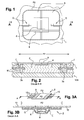
Sur les
Le module est encarté dans un corps de carte 1. Il comprend des jambes J s'étendant d'une zone sensiblement centrale de plage de contact vers une zone de connexion 3a, 3b à travers des puits. Chaque jambe J formée à l'intérieur d'une plage de contact 9 par une découpe D de celle-ci.The module is embedded in a card body 1. It comprises legs J extending from a substantially central area of the contact pad to a
Au pliage, la découpe J de la plage de contact est orientée à 90° par rapport à la surface principale du module.At folding, the cut J of the contact pad is oriented at 90 ° with respect to the main surface of the module.
Des creux correspondant à chaque découpe D apparaissent en surface du module et de la carte à puce 100.Holes corresponding to each cut D appear on the surface of the module and the
Les jambes J pénètrent dans une matière conductrice remplissant les puits et au contact des zones de connexion (sans connecter directement les zones de connexion). Les jambes sont entièrement prises dans la matière conductrice et ne connectent pas directement les zones de connexion mais à travers la matière conductrice.The legs J penetrate into a conductive material filling the wells and in contact with the connection areas (without directly connecting the connection areas). The legs are fully engaged in the conductive material and do not directly connect the connection areas but through the conductive material.
L'invention concerne un procédé de connexion de plages conductrices 10 d'un micromodule (2) à des zones de connexion 3a, 3b noyées ou accessibles dans un support 1 d'un objet portable 100.The invention relates to a method for connecting
A la
Le procédé comprend une étape de fourniture ou de réalisation d'un corps de l'objet portable 1 comportant une cavité 11 de réception du micromodule et des zones de connexion 3a, 3b accessibles dans ladite cavité. La cavité débouche en surface du corps et est délimitée à la surface du corps par une première périphérie,The method comprises a step of supplying or producing a body of the portable object 1 comprising a
Dans le premier mode de réalisation, on réalise un corps de la carte à puce avec une cavité 11 ici à deux niveaux et des plages de connexion 3a, 3b d'une antenne radiofréquence 3 enfouie dans le corps de carte. La carte est par exemple obtenue par lamination de feuilles ou surmoulage d'un circuit électrique / électronique notamment supportée per une feuille. La cavité définit une première périphérie P1 ou un pourtour de la cavité la plus étendue débouchant en surface du corps de l'objet.In the first embodiment, a body of the smart card is made with a
La cavité P1 et /ou ouvertures 5a, 5b permettant l'accès aux zones de connexion 3a, 3b du circuit d'antenne 3 peuvent être réalisées notamment par usinage ou au cours du surmoulage en ayant recours à un noyau occupant la cavité et/ou ouvertures.The cavity P1 and / or
Dans l'exemple, le corps de carte comprend un ou plusieurs percement(s) ou évidement(s) 5a, 5b qui permettent un accès aux zones de connexion 3a, 3b de l'antenne 3 à partir de l'extérieur du corps. L'antenne 3 est enfouie dans le corps de carte et comprend des zones de connexions 3a, 3B accessibles de l'extérieur du corps de carte 1.In the example, the card body comprises one or more holes (s) or recess (s) 5a, 5b which allow access to the
Le procédé comprend également une étape de réalisation d'un micromodule 2 comprenant des plages de contact électrique 10 sur une face avant délimitées par une seconde périphérie P2 correspondant sensiblement ou étant légèrement inférieure à la première périphérie P1, des portions de connexion repliées vers une face arrière du micromodule opposée à la face avant.The method also comprises a step of producing a
Le micromodule 2 comprend ici un microcircuit intégré 8. Le micromodule est ici sensiblement conforme aux micromodules de carte à puce. Il comprend ici un enrobage E, des connexions 6 de puce aux différents contacts ou plages de contact. Le module est ici de type simple face. Les plages de contact ou conductrices sont réalisées d'un seul côté du module notamment par gravure ou contre-collage de métallisations. Le côté destiné à connecter un terminal à contact est pourvu de ces plages de contacts 10.The
A la
Le micromodule comprend ici des plages de contact 11 en surface supérieure. Alternativement, les plages peuvent être sous un substrat support.The micromodule here comprises
Ces portions de plages conductrices sont ensuite repliées avant insertion dans la cavité, vers la face opposée de celle portant les plages de contact, en fait en direction du corps support 1. Ces portions 10 sont ici repliées sensiblement à 90° vers la face portant la puce.These portions of conductive pads are then folded before insertion into the cavity, towards the opposite face of that bearing the contact pads, in fact towards the support body 1. These
Les portions de plage 10 peuvent être supportées par un film diélectrique isolant. Le pliage peut être réalisé de manière à ce que la face conductrice de la portion soit orientée sensiblement dans une direction allant de la face avant vers la face arrière du module.The
Selon une caractéristique, les portions de connexion qui s'étendent à partir de la première périphérie des plages de contact, sont configurées de manière qu'en position repliées, elles puissent exercer une force de contact élastique contre les zones de connexion après insertion dans la cavité.According to one feature, the connection portions that extend from the first periphery of the contact pads are configured so that in the folded position they can exert an elastic contact force against the connection areas after insertion into the cavity.
Aux
Le procédé comprend également une étape d'insertion et de connexion du module dans la cavité, les portions de connexion étant mises en connexion électrique avec leur zone de connexion (3a, 3b) respective.The method also comprises a step of insertion and connection of the module in the cavity, the connection portions being electrically connected with their respective connection zone (3a, 3b).
Dans l'exemple, pour la connexion, le micromodule après avoir les portions repliées, est encarté de manière classique dans la cavité 11 du corps de carte et fixé avec, par exemple, une couche thermo-adhésive G, de la colle cyanoacrylate, etc. comme illustré à la
Selon une caractéristique, les portions de connexion s'étendent à partir de la première périphérie des plages de contact ; Ces portions peuvent être configurées de manière à présenter une élasticité dans une direction sensiblement perpendiculaire à la surface principale des plages de contact.According to one characteristic, the connection portions extend from the first periphery of the contact pads; These portions may be configured to have elasticity in a direction substantially perpendicular to the main surface of the contact pads.
Les portions sont dimensionnées de préférence avec une plus grande longueur que la profondeur des puits 5b, 5a de manière à être légèrement courbées notamment par flambage au cours de l'insertion. Un outil d'insertion peut exercer à cette opération, une force sur toute la surface du module pour le collage et déformation élastiques et/ou plastique des portions de connexion (jambes 10).The portions are preferably dimensioned with a greater length than the depth of the
A la
Dans ce mode de réalisation, au moins une portion 10 est configurée de manière à former un zigzag ou ressort élastique et/ou à se déformer élastiquement à l'insertion.In this embodiment, at least one
Préalablement à l'insertion, au moins une portion peut être repliée, configurée de manière à former une inclinaison vers l'intérieur du module (vers le centre du module) et à se déformer au moins élastiquement à l'insertion.Prior to insertion, at least one portion may be folded, configured to form an inward tilt of the module (toward the center of the module) and to deform at least elastically at insertion.
Alternativement le zigzag (ou plusieurs pliures sur une portion de connexion) peut être formé avant insertion notamment avant ou après le repliement des portions vers la face arrière du module.Alternatively the zigzag (or several folds on a connecting portion) can be formed before insertion including before or after the folding of the portions to the rear face of the module.
Le procédé peut comprendre une étape de comblement au moins partiel de chaque évidement (5a, 5b) par une colle ou résine conductrice ou non. La colle / résine a pour fonction de fixer la portion en position de connexion élastique contre les zones de connexion. Le cas échéant, contrairement à la figure 5D, seul le fond des puits peut être comblé de colle / résine. Ainsi, une grande partie intermédiaire de la portion de connexion 10 est libre de mouvement entre son extrémité au contact de la zone de connexion et son raccordement à la plage de contact en surface externe du module au niveau de la ligne périphérique.The method may comprise a step of at least partial filling of each recess (5a, 5b) by a glue or conductive resin or not. The adhesive / resin serves to fix the portion in the elastic connection position against the connection areas. If necessary, contrary to FIG. 5D, only the bottom of the wells can be filled with glue / resin. Thus, a large intermediate portion of the
Bien que le module possède ici plusieurs portions de connexion notamment pour connecter un ou plusieurs circuit(s) de carte multi-composant, dans d'autres modes de réalisation, il peut comporter uniquement deux portions de connexions par exemple au niveau des plages C4, C8 selon l'ISO 7816 pour connecter une antenne.Although the module here has several connection portions in particular for connecting one or more multi-component card circuit (s), in other embodiments, it may comprise only two portions of connections for example at the C4 ranges, C8 according to ISO 7816 to connect an antenna.
Claims (8)
caractérisé en ce que lesdites portions de connexion s'étendent à partir de la seconde périphérie (P2) des plages de contact et sont configurées de manière qu'en position repliée, elles exercent une force de contact contre les zones de connexion.
characterized in that said connecting portions extend from the second periphery (P2) of the contact pads and are configured such that in the folded position they exert a contact force against the connection areas.
Priority Applications (3)
| Application Number | Priority Date | Filing Date | Title |
|---|---|---|---|
| EP13305150.8A EP2765536A1 (en) | 2013-02-07 | 2013-02-07 | Method for connecting a microcircuit with accessible conductive areas in a substrate |
| EP14701070.6A EP2954462A1 (en) | 2013-02-07 | 2014-01-21 | Method for connecting a microcircuit to accessible conductive areas in a support |
| PCT/EP2014/051146 WO2014122009A1 (en) | 2013-02-07 | 2014-01-21 | Method for connecting a microcircuit to accessible conductive areas in a support |
Applications Claiming Priority (1)
| Application Number | Priority Date | Filing Date | Title |
|---|---|---|---|
| EP13305150.8A EP2765536A1 (en) | 2013-02-07 | 2013-02-07 | Method for connecting a microcircuit with accessible conductive areas in a substrate |
Publications (1)
| Publication Number | Publication Date |
|---|---|
| EP2765536A1 true EP2765536A1 (en) | 2014-08-13 |
Family
ID=47843208
Family Applications (2)
| Application Number | Title | Priority Date | Filing Date |
|---|---|---|---|
| EP13305150.8A Withdrawn EP2765536A1 (en) | 2013-02-07 | 2013-02-07 | Method for connecting a microcircuit with accessible conductive areas in a substrate |
| EP14701070.6A Withdrawn EP2954462A1 (en) | 2013-02-07 | 2014-01-21 | Method for connecting a microcircuit to accessible conductive areas in a support |
Family Applications After (1)
| Application Number | Title | Priority Date | Filing Date |
|---|---|---|---|
| EP14701070.6A Withdrawn EP2954462A1 (en) | 2013-02-07 | 2014-01-21 | Method for connecting a microcircuit to accessible conductive areas in a support |
Country Status (2)
| Country | Link |
|---|---|
| EP (2) | EP2765536A1 (en) |
| WO (1) | WO2014122009A1 (en) |
Cited By (1)
| Publication number | Priority date | Publication date | Assignee | Title |
|---|---|---|---|---|
| FR3030087A1 (en) * | 2014-12-11 | 2016-06-17 | Oberthur Technologies | MODULE FOR MICROCIRCUIT CARDS, MICROCIRCUIT CARDS COMPRISING SUCH A MODULE AND METHOD OF MANUFACTURE |
Citations (6)
| Publication number | Priority date | Publication date | Assignee | Title |
|---|---|---|---|---|
| EP0225238A1 (en) * | 1985-11-08 | 1987-06-10 | Thomson Composants Militaires Et Spatiaux | Cards comprising a component and micromodule with edge contacts |
| US5598032A (en) | 1994-02-14 | 1997-01-28 | Gemplus Card International | Hybrid chip card capable of both contact and contact-free operation and having antenna contacts situated in a cavity for an electronic module |
| US5671525A (en) * | 1995-02-13 | 1997-09-30 | Gemplus Card International | Method of manufacturing a hybrid chip card |
| US5736781A (en) * | 1993-10-18 | 1998-04-07 | Oki Electric Industry Co., Ltd. | IC module and a data carrier employing the same |
| US5856912A (en) | 1997-03-04 | 1999-01-05 | Motorola Inc. | Microelectronic assembly for connection to an embedded electrical element, and method for forming same |
| EP2450837A1 (en) * | 2010-11-04 | 2012-05-09 | Gemalto SA | Method for interconnecting by spring a conductive area to an electrical contact and corresponding device |
Family Cites Families (1)
| Publication number | Priority date | Publication date | Assignee | Title |
|---|---|---|---|---|
| FR2724477B1 (en) * | 1994-09-13 | 1997-01-10 | Gemplus Card Int | NON-CONTACT CARD MANUFACTURING PROCESS |
-
2013
- 2013-02-07 EP EP13305150.8A patent/EP2765536A1/en not_active Withdrawn
-
2014
- 2014-01-21 EP EP14701070.6A patent/EP2954462A1/en not_active Withdrawn
- 2014-01-21 WO PCT/EP2014/051146 patent/WO2014122009A1/en active Application Filing
Patent Citations (6)
| Publication number | Priority date | Publication date | Assignee | Title |
|---|---|---|---|---|
| EP0225238A1 (en) * | 1985-11-08 | 1987-06-10 | Thomson Composants Militaires Et Spatiaux | Cards comprising a component and micromodule with edge contacts |
| US5736781A (en) * | 1993-10-18 | 1998-04-07 | Oki Electric Industry Co., Ltd. | IC module and a data carrier employing the same |
| US5598032A (en) | 1994-02-14 | 1997-01-28 | Gemplus Card International | Hybrid chip card capable of both contact and contact-free operation and having antenna contacts situated in a cavity for an electronic module |
| US5671525A (en) * | 1995-02-13 | 1997-09-30 | Gemplus Card International | Method of manufacturing a hybrid chip card |
| US5856912A (en) | 1997-03-04 | 1999-01-05 | Motorola Inc. | Microelectronic assembly for connection to an embedded electrical element, and method for forming same |
| EP2450837A1 (en) * | 2010-11-04 | 2012-05-09 | Gemalto SA | Method for interconnecting by spring a conductive area to an electrical contact and corresponding device |
Cited By (1)
| Publication number | Priority date | Publication date | Assignee | Title |
|---|---|---|---|---|
| FR3030087A1 (en) * | 2014-12-11 | 2016-06-17 | Oberthur Technologies | MODULE FOR MICROCIRCUIT CARDS, MICROCIRCUIT CARDS COMPRISING SUCH A MODULE AND METHOD OF MANUFACTURE |
Also Published As
| Publication number | Publication date |
|---|---|
| EP2954462A1 (en) | 2015-12-16 |
| WO2014122009A1 (en) | 2014-08-14 |
Similar Documents
| Publication | Publication Date | Title |
|---|---|---|
| EP1062634B1 (en) | Chip card equipped with a loop antenna, and associated micromodule | |
| EP2877965B1 (en) | Electronic module for chip card and printed circuit producing such a module | |
| EP2867831B1 (en) | Methode pour la fabrication d'un microcircuit sans contact | |
| EP1834352A1 (en) | Double-sided electronic module for hybrid smart card | |
| EP2159734A1 (en) | Memory card adapter for connecting mini-card in larger connector | |
| EP3734493A1 (en) | Case for enrolment for smart card | |
| EP2718877B1 (en) | Microcircuit module and smart card comprising same | |
| EP3408799B1 (en) | Method for manufacturing a smart card module and a smart card | |
| FR3088515A1 (en) | ELECTRONIC MODULE FOR CHIP CARD | |
| EP1724712A1 (en) | Micromodule, specifically for a smart card | |
| EP2765536A1 (en) | Method for connecting a microcircuit with accessible conductive areas in a substrate | |
| EP3059698B1 (en) | Method for manufacturing a single-surface electronic module including interconnection areas | |
| WO2015132485A1 (en) | Simplified electronic module for a smartcard with a dual communication interface | |
| FR2780534A1 (en) | Fabrication method for portable objects incorporating electronic components, particularly non-contact smart cards | |
| EP1556832B1 (en) | Smart card comprising a protruding component and method for making same | |
| FR2797075A1 (en) | METHOD FOR MANUFACTURING PORTABLE DEVICE WITH INTEGRATED CIRCUITS, TYPE CHIP CARD WITH REDUCED FORMAT FORMAT IN RELATION TO STANDARD FORMAT | |
| WO2020114753A1 (en) | Method for manufacturing a metal or non-metal chip card with relay antenna | |
| EP2575086A1 (en) | Method for connecting a microcircuit with conductive areas embedded in a medium | |
| EP3391293A1 (en) | Method for fabricating a device comprising a radiofrequency electronic module and an indicator | |
| FR3086098A1 (en) | METHOD FOR MANUFACTURING AN ELECTRONIC MODULE FOR A PORTABLE OBJECT | |
| FR3084188A1 (en) | CHIP CARD EQUIPPED WITH A PLURALITY OF ANTENNAS | |
| EP3166181A1 (en) | Method for manufacturing a radiofrequency antenna on a mounting and antenna thus obtained | |
| FR3076375A1 (en) | BOOSTER ANTENNA FOR CONTACTLESS CHIP CARD | |
| FR3030087A1 (en) | MODULE FOR MICROCIRCUIT CARDS, MICROCIRCUIT CARDS COMPRISING SUCH A MODULE AND METHOD OF MANUFACTURE |
Legal Events
| Date | Code | Title | Description |
|---|---|---|---|
| PUAI | Public reference made under article 153(3) epc to a published international application that has entered the european phase |
Free format text: ORIGINAL CODE: 0009012 |
|
| 17P | Request for examination filed |
Effective date: 20130207 |
|
| AK | Designated contracting states |
Kind code of ref document: A1 Designated state(s): AL AT BE BG CH CY CZ DE DK EE ES FI FR GB GR HR HU IE IS IT LI LT LU LV MC MK MT NL NO PL PT RO RS SE SI SK SM TR |
|
| AX | Request for extension of the european patent |
Extension state: BA ME |
|
| STAA | Information on the status of an ep patent application or granted ep patent |
Free format text: STATUS: THE APPLICATION IS DEEMED TO BE WITHDRAWN |
|
| 18D | Application deemed to be withdrawn |
Effective date: 20150214 |