EP2784831A1 - Semiconductor device and method for manufacturing the same - Google Patents
Semiconductor device and method for manufacturing the same Download PDFInfo
- Publication number
- EP2784831A1 EP2784831A1 EP14168448.0A EP14168448A EP2784831A1 EP 2784831 A1 EP2784831 A1 EP 2784831A1 EP 14168448 A EP14168448 A EP 14168448A EP 2784831 A1 EP2784831 A1 EP 2784831A1
- Authority
- EP
- European Patent Office
- Prior art keywords
- light
- semiconductor device
- optical semiconductor
- layer
- emitting layers
- Prior art date
- Legal status (The legal status is an assumption and is not a legal conclusion. Google has not performed a legal analysis and makes no representation as to the accuracy of the status listed.)
- Withdrawn
Links
Images


Classifications
-
- H—ELECTRICITY
- H01—ELECTRIC ELEMENTS
- H01L—SEMICONDUCTOR DEVICES NOT COVERED BY CLASS H10
- H01L33/00—Semiconductor devices with at least one potential-jump barrier or surface barrier specially adapted for light emission; Processes or apparatus specially adapted for the manufacture or treatment thereof or of parts thereof; Details thereof
- H01L33/48—Semiconductor devices with at least one potential-jump barrier or surface barrier specially adapted for light emission; Processes or apparatus specially adapted for the manufacture or treatment thereof or of parts thereof; Details thereof characterised by the semiconductor body packages
- H01L33/50—Wavelength conversion elements
- H01L33/507—Wavelength conversion elements the elements being in intimate contact with parts other than the semiconductor body or integrated with parts other than the semiconductor body
-
- H—ELECTRICITY
- H01—ELECTRIC ELEMENTS
- H01L—SEMICONDUCTOR DEVICES NOT COVERED BY CLASS H10
- H01L33/00—Semiconductor devices with at least one potential-jump barrier or surface barrier specially adapted for light emission; Processes or apparatus specially adapted for the manufacture or treatment thereof or of parts thereof; Details thereof
- H01L33/005—Processes
- H01L33/0093—Wafer bonding; Removal of the growth substrate
-
- H—ELECTRICITY
- H01—ELECTRIC ELEMENTS
- H01L—SEMICONDUCTOR DEVICES NOT COVERED BY CLASS H10
- H01L33/00—Semiconductor devices with at least one potential-jump barrier or surface barrier specially adapted for light emission; Processes or apparatus specially adapted for the manufacture or treatment thereof or of parts thereof; Details thereof
- H01L33/48—Semiconductor devices with at least one potential-jump barrier or surface barrier specially adapted for light emission; Processes or apparatus specially adapted for the manufacture or treatment thereof or of parts thereof; Details thereof characterised by the semiconductor body packages
- H01L33/50—Wavelength conversion elements
- H01L33/505—Wavelength conversion elements characterised by the shape, e.g. plate or foil
-
- H—ELECTRICITY
- H01—ELECTRIC ELEMENTS
- H01L—SEMICONDUCTOR DEVICES NOT COVERED BY CLASS H10
- H01L33/00—Semiconductor devices with at least one potential-jump barrier or surface barrier specially adapted for light emission; Processes or apparatus specially adapted for the manufacture or treatment thereof or of parts thereof; Details thereof
- H01L33/48—Semiconductor devices with at least one potential-jump barrier or surface barrier specially adapted for light emission; Processes or apparatus specially adapted for the manufacture or treatment thereof or of parts thereof; Details thereof characterised by the semiconductor body packages
- H01L33/52—Encapsulations
- H01L33/56—Materials, e.g. epoxy or silicone resin
-
- H—ELECTRICITY
- H01—ELECTRIC ELEMENTS
- H01L—SEMICONDUCTOR DEVICES NOT COVERED BY CLASS H10
- H01L33/00—Semiconductor devices with at least one potential-jump barrier or surface barrier specially adapted for light emission; Processes or apparatus specially adapted for the manufacture or treatment thereof or of parts thereof; Details thereof
- H01L33/48—Semiconductor devices with at least one potential-jump barrier or surface barrier specially adapted for light emission; Processes or apparatus specially adapted for the manufacture or treatment thereof or of parts thereof; Details thereof characterised by the semiconductor body packages
- H01L33/62—Arrangements for conducting electric current to or from the semiconductor body, e.g. lead-frames, wire-bonds or solder balls
-
- H—ELECTRICITY
- H01—ELECTRIC ELEMENTS
- H01L—SEMICONDUCTOR DEVICES NOT COVERED BY CLASS H10
- H01L2924/00—Indexing scheme for arrangements or methods for connecting or disconnecting semiconductor or solid-state bodies as covered by H01L24/00
- H01L2924/0001—Technical content checked by a classifier
- H01L2924/0002—Not covered by any one of groups H01L24/00, H01L24/00 and H01L2224/00
-
- H—ELECTRICITY
- H01—ELECTRIC ELEMENTS
- H01L—SEMICONDUCTOR DEVICES NOT COVERED BY CLASS H10
- H01L33/00—Semiconductor devices with at least one potential-jump barrier or surface barrier specially adapted for light emission; Processes or apparatus specially adapted for the manufacture or treatment thereof or of parts thereof; Details thereof
- H01L33/36—Semiconductor devices with at least one potential-jump barrier or surface barrier specially adapted for light emission; Processes or apparatus specially adapted for the manufacture or treatment thereof or of parts thereof; Details thereof characterised by the electrodes
- H01L33/38—Semiconductor devices with at least one potential-jump barrier or surface barrier specially adapted for light emission; Processes or apparatus specially adapted for the manufacture or treatment thereof or of parts thereof; Details thereof characterised by the electrodes with a particular shape
-
- H—ELECTRICITY
- H01—ELECTRIC ELEMENTS
- H01L—SEMICONDUCTOR DEVICES NOT COVERED BY CLASS H10
- H01L33/00—Semiconductor devices with at least one potential-jump barrier or surface barrier specially adapted for light emission; Processes or apparatus specially adapted for the manufacture or treatment thereof or of parts thereof; Details thereof
- H01L33/44—Semiconductor devices with at least one potential-jump barrier or surface barrier specially adapted for light emission; Processes or apparatus specially adapted for the manufacture or treatment thereof or of parts thereof; Details thereof characterised by the coatings, e.g. passivation layer or anti-reflective coating
Definitions
- the present invention relates to an optical semiconductor device and a method for manufacturing the same.
- an optical semiconductor device that emits white light by using an optical semiconductor element that emits blue light and a phosphor capable of wavelength conversion from blue light into yellow light.
- Such an optical semiconductor device that emits white light has characteristics of: being small in size; emitting high-intensity light relative to a supplied power amount; having a long life; and using no toxic substance such as mercury. These characteristics allow the optical semiconductor device to be increasingly used in various fields such as application to an under-button light source or a flash light source for portable phone and application to an interior light source and an exterior light source for vehicle.
- an optical semiconductor device using blue LEDs currently has an efficiency of 150 lm/W, which is larger than those of conventional light sources such as an incandescent light bulb (15 lm/W to 20 lm/W) and a fluorescent lamp (60 lm/W to 90 lm/W) .
- conventional light sources such as an incandescent light bulb (15 lm/W to 20 lm/W) and a fluorescent lamp (60 lm/W to 90 lm/W) .
- the optical semiconductor device has a problem of requiring cost more than ten times higher than the conventional light sources which require 0.1 yen/lm to 0.2 yen/lm.
- As a measure to reduce the cost there has been studied a structure of an optical semiconductor device allowing cost reduction while enhancing the luminous efficiency of an element therein.
- the most general optical semiconductor device that has been commercialized has a structure including: an optical semiconductor element that emits blue light; an Ag-plated Cu frame formed of a white thermoplastic resin by molding, and used as a wiring board; a connection material for connecting the optical semiconductor element and the frame; a gold wire through which a current flows between the frame and a top surface electrode of the optical semiconductor element; and a silicone resin mixed with phosphor particles for wavelength conversion from blue light into yellow light and sealing in the optical semiconductor element (see JP-A No. 2000-183407 (KOKAI) for example).
- a white thermoplastic resin is firstly formed into the Ag-plated Cu frame by molding. Then, a connection resin is applied onto a portion, on which the optical semiconductor element is to be mounted, of the frame. Thereafter, the optical semiconductor element is mounted on the portion, and the connection resin is hardened by heating in an oven. Thereby, the optical semiconductor element is connected to the frame. Then, by using a wire bonder, the electrode formed on the chip top surface of the optical semiconductor element is connected to the frame with an Au wire. Thereafter, a silicone resin with a phosphor concentration adjusted to allow the optical semiconductor device to emit white light is applied, by a dispense technique, around the portion in which the optical semiconductor element is mounted, and then hardened by heating. Lastly, a product portion including the optical semiconductor element is cut off, and the frame used as an exterior electrode is finished by a forming process. Thereby, the optical semiconductor device is completed.
- a conventional optical semiconductor device is manufactured by incorporating a blue light semiconductor element in a structure of an optical semiconductor device that, in most cases, has been commercialized using an optical semiconductor element that emits light having a wavelength of 500 nm or more.
- the optical semiconductor device that emits such long-wavelength light has a high directivity and has thus been applied to devices for vehicle, display panels, amusement machines and the like.
- Such a conventional optical semiconductor device manufactured as above has a problem of having a shorter life for reasons, such as that blue light, which has a short wavelength and a high intensity, discolors a reflector resin having benzene ring.
- an optical semiconductor device that emits white light commercialized in response to the development of a high-intensity optical semiconductor element that emits blue light has been increasingly applied to lighting apparatuses as well as conventionally-applied apparatuses such as devices for vehicle and display panels. With this trend, cost reduction of the optical semiconductor device has been indispensably required.
- the conventional structure of an optical semiconductor device only allows limited cost reduction, and thus the structure and the manufacturing process of the optical semiconductor device has been required to be reconsidered.
- an optical semiconductor device when an optical semiconductor device is applied to a lighting apparatus, a light source therein cannot be formed of a single optical semiconductor device. Accordingly, in order to replace a general lighting apparatus, such as a fluorescent lamp, with an apparatus using an optical semiconductor device that emits white light, the apparatus needs to include multiple optical semiconductor devices. In this case, to eliminate defects such as nonuniform intensity in a light-emitting surface, a large number of small optical semiconductor devices need to be mounted on a wiring board. Accordingly, the size reduction of the optical semiconductor device has also been required.
- An object of the present invention is to provide an optical semiconductor device that is capable of suppressing the life reduction thereof, that can be manufactured at reduced cost, and that can be miniaturized approximately to the size of an optical semiconductor element, and to provide a method for manufacturing such an optical semiconductor device.
- a first aspect according to an embodiment of the present invention is an optical semiconductor device includes: a light-emitting layer having a first main surface, a second main surface opposed to the first main surface, a first electrode and a second electrode which are formed on the second main surface; a fluorescent layer containing phosphor particles and provided on the first main surface; a light-transmissive layer provided on the fluorescent layer and made of a light-transmissive inorganic material; a first metal post provided on the first electrode; a second metal post provided on the second electrode; a sealing layer provided on the second main surface so as to seal in the first and second metal posts with one ends of the respective first and second metal posts exposed; a first metal layer provided on the exposed end of the first metal post; and a second metal layer provided on the exposed end of the second metal post.
- a second aspect according to an embodiment of the present invention is a method for manufacturing an optical semiconductor device, includes: manufacturing a light-emitting substrate by forming multiple groups of positive and negative electrodes on a first main surface of a light-emitting layer, the positive and negative electrodes being used to cause a current for exciting the light-emitting layer to flow through the light-emitting layer; manufacturing a fluorescent substrate by forming, on a light-transmissive inorganic film, a fluorescent layer made of a resin in which phosphor particles are dispersed; bonding the fluorescent layer of the fluorescent substrate onto a second main surface of the light-emitting layer which is opposed to the first main surface; and separating the bonded substrate into pieces each including one of the groups of the positive and negative electrodes.
- a third aspect according to an embodiment of the present invention is a method for manufacturing an optical semiconductor device, includes: forming multiple light-emitting layers on a substrate, the light-emitting layers each having a first main surface, a second main surface opposed to the first main surface, a first electrode and a second electrode which are formed on the second main surface; forming a conductive film on the substrate, on which the multiple light-emitting layers are formed, so that the conductive film covers the multiple light-emitting layers; forming a sacrifice layer on the conductive film, the sacrifice layer having openings located respectively on the first and second electrodes of all of the light-emitting layers; forming plated layers respectively on the first and second electrodes of all of the light-emitting layers by electroplating using the conductive film as a negative electrode; removing the sacrifice layer and the conductive film from the substrate on which the plated layers are formed; forming a sealing layer on the substrate from which the sacrifice layer and the conductive film are removed, the sealing layer sealing in the plated layers of all
- a fourth aspect according to an embodiment of the present invention is a method for manufacturing an optical semiconductor device, includes: forming multiple light-emitting layers on a substrate, the light-emitting layers each having a first main surface, a second main surface opposed to the first main surface, a first electrode and a second electrode which are formed on the second main surface; forming a conductive film on the substrate, on which the multiple light-emitting layers are formed, so that the conductive film covers the multiple light-emitting layers; forming a sacrifice layer on the conductive film, the sacrifice layer having openings located respectively on the first and second electrodes of all of the light-emitting layers; forming plated layers respectively on the first and second electrodes of all of the light-emitting layers by electroplating using the conductive film as a negative electrode; removing the sacrifice layer and the conductive film from the substrate on which the plated layers are formed; forming a sealing layer on the substrate from which the sacrifice layer and the conductive film are removed, the sealing layer sealing in the plated layers of all
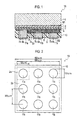
- an optical semiconductor device 1A includes: a light-emitting layer 2, an adhesive layer 3, a fluorescent layer 4, a light-transmissive layer 5, a reflective layer 6, a first electrode 7a, multiple second electrodes 7b, a first metal post 8a, multiple second metal posts 8b, an insulating layer 9, a sealing layer 10, a first metal layer 11a and multiple second metal layers 11b.
- the light-emitting layer 2 has a first main surface M1 and a second main surface M2.
- the adhesive layer 3, the fluorescent layer 4 and the light-transmissive layer 5 are sequentially provided on the first main surface M1.
- the reflective layer 6 is provided on a first region of the second main surface M2 of the light-emitting layer 2.
- the first electrode 7a is provided on a second region of the second main surface M2.
- the second electrodes 7b are provided on the reflective layer 6.
- the first metal post 8a is provided on the first electrode 7a.
- the second metal posts 8b are provided on the respective second electrodes 7b.
- the insulating layer 9 is provided on regions, other than those with the metal posts 8a and 8b, of the second main surface M2 of the light-emitting layer 2.
- the sealing layer 10 is provided on the insulating layer 9 so as to seal in the metal posts 8a and 8b.
- the first metal layer 11a is provided on one end of the first metal post 8a.
- the second metal layers 11b are provided on one ends of the second metal posts 8b, respectively.
- the light-emitting layer 2 is formed of first and second cladding layers 2a and 2b, and an active layer 2c.
- the first cladding layer 2a is an n-type semiconductor layer.
- the second cladding layer 2b is a p-type semiconductor layer, and is smaller in area than the first cladding layer 2a.
- the active layer 2c is held between the first and second cladding layers 2a and 2b.
- the light-emitting layer 2 has a thickness of 5 ⁇ m, and is formed, for example, of InGaN layers that emit blue light. Note that the upper surface (in FIG. 1 ) of the first cladding layer 2a serves as the first main surface M1, and the lower surface (in FIG. 1 ) of the second cladding layer 2b and part of the lower surface (in FIG. 1 ) of the first cladding layer 2a collectively serve as the second main surface M2, which has a step.
- the planar shape of the first cladding layer 2a is a square 550 ⁇ m on a side (see the dotted line of FIG. 2 ).
- the second cladding layer 2b is formed with the active layer 2c interposed therebetween.
- the active layer 2c has the same shape and approximately the same area as the second cladding layer 2b.
- the adhesive layer 3 is made of a silicone resin.
- the adhesive layer 3 has a thickness not more than 1 ⁇ m, for example, and bonds the fluorescent layer 4 and the first main surface M1 of the first cladding layer 2a of the light-emitting layer 2 together.
- the silicone resin methyl phenyl silicone having a refractive index of approximately 1.5 is used.
- a resin for sealing in phosphor particles methyl phenyl silicone or a silicone resin different in composition, such as dimethyl silicone, may be used. Alternatively, as long as appropriate for the intended use, another resin may be used.
- a resin such as an epoxy resin, a hybrid resin of an epoxy resin and a silicone resin, or a urethane resin may be used as the sealing resin.
- the fluorescent layer 4 is formed by mixing phosphor particles in a silicone resin.
- the phosphor particles convert blue light into long-wavelength light.
- the fluorescent layer 4 has a thickness of 15 ⁇ m, for example.
- the silicone resin methyl phenyl silicone having a refractive index of approximately 1.5, which is also used for the adhesive layer 3, is used.
- the silicone resin used for the fluorescent layer 4 is not limited to this, but may be another resin.
- the phosphor used is YAG:Ce, which is yttrium aluminate doped with cerium as an activator and which has a particle diameter not more than 10 ⁇ m
- (Sr, Ba) 2 SiO 4 which is strontium-barium silicate doped with europium as an activator
- Ca p (Si, Al) 12 or the like may be used according to need.
- the mixed phosphor need not necessarily be made of a material having a single composition, but may be made of a mixture of two materials: one for wavelength conversion from blue light into green light; the other for wavelength conversion from blue light into red light.
- the light-transmissive layer 5 is made of a transparent substrate made of a material such as optical glass or quartz.
- the light-transmissive layer 5 has a thickness of 200 ⁇ m, for example.
- the material of the light-transmissive layer 5 is not limited to the transparent substrate, but may be another light-transmissive material.
- the light-transmissive layer 5 needs only to be made of a light-transmissive substrate made of a light-transmissive inorganic material.
- a substrate having as a low refractive index as possible within a range from 1.0 to 2.0 should preferably be used as the light-transmissive substrate. This reduces a difference in refractive index between the fluorescent layer 4 and the air, and thus can improve the light extraction efficiency of the optical semiconductor device 1A.
- the reflective layer 6 is made of a metal such as Ag or A1, and has a thickness of 0.3 ⁇ m, for example.
- the reflective layer 6 is provided on the entire region (first region) of the lower surface (in FIG. 1 ) of the second cladding layer 2b in the light-emitting layer 2.
- an Ni/Au contact electrode (not shown) is formed by depositing metals such as Ni and Au in a thickness of 0.1 ⁇ m/0.1 ⁇ m on the lower surface of the second cladding layer 2b, and the reflective layer 6 having a thickness of 0.3 ⁇ m is then formed thereon.
- the first electrode 7a is formed by depositing metals such as Ni and Au in a thickness of 0.1 ⁇ m/0.1 ⁇ m, and thus has a thickness of 0.2 ⁇ m.
- the first electrode 7a which is formed in a circle having a diameter of 100 ⁇ m, is provided on an exposed region (second region) of the lower surface (in FIG. 1 ) of the first cladding layer 2a in the light-emitting layer 2 (see FIG. 2 ).
- Each second electrode 7b is also formed by depositing metals such as Ni and Au in a thickness of 0.1 ⁇ m/0.1 ⁇ m, and thus has a thickness of 0,2 ⁇ m.
- the second electrodes 7b, each of which is formed in a circle having a diameter of 100 ⁇ m, are provided on the lower surface (in FIG. 1 ) of the reflective layer 6 with a 200 ⁇ m pitch (see FIG. 2 ).
- the first metal post 8a is formed of a metal such as Cu to have a columnar shape.
- the first metal post 8a has a height of approximately 103 ⁇ m and a diameter of 100 ⁇ m.
- a current flows between the first metal post 8a and the first electrode 7a. Note that the shapes of the first electrode 7a and the first metal post 8a may be changed according to need.
- Each second metal post 8b is formed of a metal such as Cu to have a columnar shape.
- the second metal post 8b has a height of approximately 100 ⁇ m and a diameter of 100 ⁇ m.
- a current flows between the second metal post 8b and the corresponding second electrode 7b.
- the second metal posts 8b are provided with a 200 ⁇ m pitch (see FIG. 2 ). Note that the shapes of the second electrodes 7b and the second metal posts 8b may be changed according to need.
- the insulating layer 9 is made of SiO 2 , and functions as a passivation film (protective film).
- the insulating layer 9 has a thickness of 0.3 ⁇ m.
- the insulating layer 9 entirely covers the light-emitting layer 2 including the ends thereof, and thus prevents a current from flowing from the outside into the light-emitting layer 2 excluding the first and second electrodes 7a and 7b. This can prevent defects such as short circuit attributable to the phenomenon that mounting solder creeps up.
- the sealing layer 10 is formed of a thermosetting resin, and has a thickness of approximately 100 ⁇ m like the metal posts 8a and 8b.
- the sealing layer 10 is provided on the entire surface of the insulating layer 9 so as to seal in the first and second metal posts 8a and 8b while leaving one ends thereof exposed. Accordingly, the circumferential surface of each of the first and second metal posts 8a and 8b is completely covered with the sealing layer 10.
- Each of the first and second metal layers 11a and 11b is formed by depositing metals such as Ni and Au in a thickness of 0.1 ⁇ m/0.1 ⁇ m.
- the first metal layer 11a is provided on the end, that is, the exposed portion, of the first metal post 8a.
- Each second metal layer 11b is provided on the end, that is, the exposed portion, of the corresponding second metal post 8b. Note that the first metal layer 11a has the same circular planar shape as the first electrode 7a, and each second metal layer 11b has the same circular planar shape as each second electrode 7b (see FIG. 2 ).
- the resultant potential is supplied to the first cladding layer 2a through the first metal post 8a, and the resultant potential is supplied to the second cladding layer 2b through the second metal posts 8b.
- light beams are emitted from the active layer 2c held between the first and second cladding layers 2a and 2b. Some of the emitted light beams are transmitted through the light-transmissive layer 5, and emitted from the surface of the light-transmissive layer 5 without reflection.
- Some of the emitted light beams are reflected by the reflective layer 6, then transmitted through the light-transmissive layer 5, and emitted from the surface of the light-transmissive layer 5. Others are incident on the phosphor particles included in the fluorescent layer 4, so that the phosphor particles are excited to emit light beams. Some of the light beams emitted from the phosphor particles are also transmitted through the light-transmissive layer 5, and emitted from the surface of the light-transmissive layer 5. Others are also reflected by the reflective layer 6, then transmitted through the light-transmissive layer 5, and emitted from the surface of the light-transmissive layer 5.
- the blue light beams emitted from the light-emitting layer 2 and the (yellow, or red and green) light beams emitted from the phosphor particles that are excited by the blue light beams are mixed into white light, which is emitted from the surface of the light-transmissive layer 5.
- the optical semiconductor device 1A is simplified in configuration, and miniaturized to have a plane area as small as that of the light-emitting layer 2.
- the structure eliminates the need for molding, a mounting step and a connecting step in manufacturing the optical semiconductor device 1A. Accordingly, the optical semiconductor device 1A can be manufactured by using normal semiconductor manufacturing equipment, and thus can be manufactured at reduced cost.
- the fluorescent layer 4 for wavelength conversion from blue light into long-wavelength light is formed on the light-emitting layer 2, and the reflective layer 6 is formed under the lower surface of the light-emitting layer 2 (in FIG. 1 ).
- the light-emitting layer 2 by causing the light-emitting layer 2 to emit blue light only upward, white light can be emitted toward the top surface (in FIG. 1 ) of the optical semiconductor device 1A.
- the light-transmissive layer 5 formed on the fluorescent layer 4 reduces the refractive index difference between the fluorescent layer 4 and the air, which allows the optical semiconductor device 1A to have improved light extraction efficiency.
- the above-mentioned structure allows the optical semiconductor device 1A, which has a plane area as small as that of the light-emitting layer 2, to be reliably mounted on a glass epoxy board, which is a typical wiring board. This is because the metal posts 8a and 8b reduce the linear expansion coefficient difference between the light-emitting layer 2 and the glass epoxy board.
- the optical semiconductor device 1A having the above-described structure is obtained as follows. Firstly, the fluorescent layer 4 is provided on the light-emitting layer 2, and a light-transmissive inorganic material is then deposited on the fluorescent layer 4 so as to serve as the light-transmissive layer 5. Thereafter, the first metal post 8a is provided on the first electrode 7a of the light-emitting layer 2, and the second metal posts 8b are provided on the respective second electrodes 7b of the light-emitting layer 2. Then, the sealing layer 10 is provided on the light-emitting layer 2 so as to seal in the first and second metal posts 8a and 8b.
- the light-transmissive layer 5 is made of an inorganic material, and thus prevented from being degraded by light (blue light, in particular) emitted from the light-emitting layer 2. Accordingly, the life reduction of the optical semiconductor device 1A is suppressed.
- the optical semiconductor device 1A may be manufactured at reduced cost. Accordingly, cost reduction of the optical semiconductor device 1A can be achieved.
- the optical semiconductor device 1A can be miniaturized approximately to the size of a typical optical semiconductor element.
- the first metal layer 11a and the second metal layers 11b are solder bumps.
- a hemispherical solder bump having a diameter of 100 ⁇ m is formed on each of the first and second metal posts 8a and 8b.
- the solder bump is made of a solder material used for surface mounting, such as Sn-3.0Ag-0.5Cu, Sn-0.8Cu and Sn-3.5Ag.
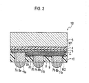
- the second embodiment of the present invention can provide the same effects as the first embodiment.
- the optical semiconductor device 1B since the first metal layer 11a and the second metal layers 11b are formed of solder bumps, the optical semiconductor device 1B has a larger gap from a wiring board on which the optical semiconductor device 1B is mounted than the optical semiconductor device 1A according to the first embodiment. Accordingly, when the optical semiconductor device 1B is mounted on the wiring board, a stress attributable to the linear expansion coefficient difference between the optical semiconductor device 1B and the wiring board can be further reduced.
- the first electrode 7a is formed as a square 100 ⁇ m on a side on the lower surface (in FIG. 4 ) of the first cladding layer 2a.
- the second electrode 7b is formed as a square 500 ⁇ m on a side with a square 150 ⁇ m on a side cut out. Specifically, the cutout portion corresponds to the corner region of the first cladding layer 2a.
- the first metal post 8a is a rectangular column having the same planar shape as the first electrode 7a
- the second metal post 8b is a rectangular column having the same planar shape as the second electrode 7b
- the first metal layer 11a has the same planar shape as the first electrode 7a
- the second metal layer 11b has the same planar shape as the second electrode 7b (see FIG. 5 ).
- the third embodiment of the present invention can provide the same effects as the first embodiment.
- the plane area of each of the first and second electrodes 7a and 7b is increased, and thus the plane area of each of the first and second metal posts 8a and 8b is increased, compared to the optical semiconductor device 1A according to the first embodiment,
- a fourth embodiment of the present invention will be described.
- the same parts as those in the first embodiment are denoted by the same reference numerals, and the description thereof is omitted.
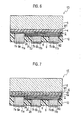
- an optical semiconductor device 1D does not include the adhesive layer 3, and the fluorescent layer 4 is formed directly on the first main surface M1 of the light-emitting layer 2.
- the fluorescent layer 4 has a thickness of 10 ⁇ m, and is formed on the first main surface M1 of the light-emitting layer 2 by a method such as sputtering or chemical vapor deposition (CVD).
- the light-transmissive layer 5 is formed on the fluorescent layer 4 by, for example, applying a liquid glass onto the fluorescent layer 4 by spin coating, and then hardening the liquid glass.
- the fourth embodiment of the present invention can provide the same effects as the first embodiment. Moreover, the above-described structure can eliminate, from the manufacturing process, a step of blending phosphor particles with a silicone resin and a step of bonding the fluorescent layer 4 onto the light-emitting layer 2, both of which are needed in the manufacturing process of the optical semiconductor device 1A according to the first embodiment. Thus, the fourth embodiment can reduce the manufacturing process time and the cost.
- a fifth embodiment of the present invention will be described.
- the same parts as those in the first embodiment are denoted by the same reference numerals, and the description thereof is omitted.
- an optical semiconductor device 1E does not include the adhesive layer 3, and the fluorescent layer 4 is formed directly on the first main surface M1 of the light-emitting layer 2.
- the fluorescent layer 4 consists of two layers, namely, fluorescent layers 4a and 4b respectively made of materials mutually different in composition. Specifically, on the light-emitting layer 2, sequentially formed are the fluorescent layer 4a for wavelength conversion from blue light into green light, and the fluorescent layer 4b for wavelength conversion from blue light into red light.
- Each of the fluorescent layers 4a and 4b has a thickness of 10 ⁇ m, and is formed on the first main surface M1 of the light-emitting layer 2 by a method such as sputtering or chemical vapor deposition (CVD).
- the light-transmissive layer 5 is formed on the fluorescent layer 4 by, for example, applying a liquid glass onto the fluorescent layer 4b by spin coating, and then hardening the liquid glass.
- the fifth embodiment of the present invention can provide the same effects as the first embodiment. Moreover, the above-described structure can eliminate, from the manufacturing process, a step of blending phosphor particles with a silicone resin and a step of bonding the fluorescent layer 4 onto the light-emitting layer 2, both of which are needed in the manufacturing process of the optical semiconductor device 1A according to the first embodiment. Thus, the fifth embodiment can reduce the manufacturing process time and the cost.
- a sixth embodiment of the present invention will be described.
- a method for manufacturing the optical semiconductor device 1A according to the first embodiment will be described. Note that this manufacturing method can be used as a method for manufacturing the optical semiconductor device 1C according to the third embodiment.
- the same parts as those in the first embodiment are denoted by the same reference numerals, and the description thereof is omitted.
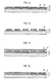
- InGaN light-emitting layers 12 that emit blue light are formed on a substrate 11, which is a sapphire wafer having a diameter of two inches and a thickness of 200 ⁇ m.
- a light-emitting layer is formed by epitaxial growth, and then separated into the light-emitting layers 12 by reactive ion etching (RIE), In this way, the light-emitting layer 2 of the optical semiconductor device 1A is formed.
- RIE reactive ion etching
- the light-emitting layer 2 is formed by forming the first cladding layer 2a on a square region 550 ⁇ m on a side, and then forming the second cladding layer 2b on a region, not including a corner region (a square 150 ⁇ m on a side), of the lower surface of the first cladding layer 2a with the active layer 2c interposed therebetween (see FIGs. 1 and 2 ).
- multi-layer films 13 are formed on the respective light-emitting layers 12 on the substrate 11.
- Ni/Au films (not shown) having a thickness of 0.1 ⁇ m/0.1 ⁇ m are firstly formed on the entire surfaces of the light-emitting layers 12 by sputtering so as to serve as contact layers of the light-emitting layers 12, respectively.
- metal films (not shown) made of Ag or Al and having a thickness of 0.3 ⁇ m are formed on the respective Ni/Au films by sputtering. In this way, the reflective layer 6 of the optical semiconductor device 1A is formed.
- Ni/Au films (not shown) having a thickness of 0.1 ⁇ m/0.1 ⁇ m, which are to be formed into electrodes, are respectively formed on electrode portions of the light-emitting layers 12.
- SiO 2 passivation films (not shown) having a thickness of 0.3 ⁇ m are formed by sputtering on regions other than the electrode portions of the light-emitting layers 12. In this way, the first electrode 7a, the second electrodes 7b and the insulating layer 9 of the optical semiconductor device 1A are formed.
- the multi-layer films 13 are formed on the respective light-emitting layers 12 on the substrate 11.
- a seed layer 14 which is a conductive film serving as a power feeding layer for plating, is formed on the entire surface of the substrate 11 by a physical deposition method such as vapor deposition or sputtering.
- a multi-layer film such as a Ti/Cu film is used.
- the Ti/Cu film which is formed to increase adhesion strength between the seed layer 14 and a resist or pads, needs only to have a thickness as small as 0.1 ⁇ m.
- the Cu layer which mainly contributes to power feeding, should preferably have a thickness not smaller than 0.2 ⁇ m.
- a resist layer 15 serving as a sacrifice layer is formed on the entire surface of the substrate 11.
- the resist layer 15 has openings at electrode pad portions which are to be formed into the first and second electrodes 7a and 7b.
- a photosensitive liquid resist or a dry film resist may be used as the resist.
- the resist layer 15 is formed on the entire surface of the substrate 11 by forming a resist layer on the substrate 11, and then forming the openings in this resist layer by exposure and development using a light shield mask. After development, the resist may be baked depending on its material.
- plated layers 16 are formed by electroplating in the respective openings of the resist layer 15.
- the metal posts 8a and 8b of the optical semiconductor device 1A are formed.
- the substrate 11 which is a wafer, is immersed in a plating liquid consisting of materials such as copper sulphate and sulphuric acid.
- a plating liquid consisting of materials such as copper sulphate and sulphuric acid.
- current is caused to flow through the substrate 11 by connecting the seed layer 14 to the negative terminal of a direct-current power source, and connecting a Cu plate, serving as an anode, to the positive terminal of the direct-current power source, and thus Cu plating starts.
- the Cu plate is placed so as to face the to-be-plated surface of the substrate 11. Before the thickness of the plated layer, which increases with time, reaches that of the resist layer 15, the current is stopped, and thus the plating is completed.
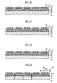
- the resist layer 15 is peeled off the substrate 11, and then the seed layer 14 is etch removed by acid cleaning. Thereby, the light-emitting layers 12, the multi-layer films 13 and the plated layers 16 are exposed.
- thermosetting resin layer 17 to serve as a sealing layer is formed on the entire surface of the substrate 11. Specifically, a thermosetting resin is applied by spin coating around the plated layers 16 in a thickness to allow the plated layers 16 embedded therein. Thereafter, the resultant substrate 11 is put in an oven and heated, and thus the thermosetting resin layer 17 is hardened.
- the resin can be hardened by being heated at 150°C for two hours, for example.
- thermosetting resin layer 17 is ground off so that ends of the respective plated layers 16 can be exposed.
- the thermosetting resin layer 17 is grounded by rotational grinding using a rotational grinding wheel, and thus the surface thereof can be planarized after being ground.
- the substrate 11 may be dried according to need. Note that, in the previous step, it is difficult to apply a thermosetting resin by a method such as spin coating with only the ends of the plated layers 16 exposed (It requires much time and cost). Accordingly, this grinding step is necessary for exposing the ends of the plated layers 16 after the spin coating step.
- the light-emitting layers 12 are lifted off the substrate 11 by irradiating the interface between the substrate 11 and the light-emitting layers 12 with laser beams.
- a light-emitting substrate 12A formed of the light-emitting layers 12, the multi-layer films 13, the plated layers 16 and the thermosetting resin layer 17 is separated off the substrate 11.
- the light-emitting layers 12 are lifted off the substrate 11 by causing an Nd:YAG third harmonic laser to irradiate the interface therebetween with laser beams. having a wavelength of 355 nm through the substrate 11. Note that the liftoff step is optional, and thus may be omitted.
- the surface, at which the light-emitting layers 12 are exposed, of the light-emitting substrate 12A formed by this liftoff step is bonded onto a fluorescent layer 19 that is provided on a light-transmissive substrate 18, such as an optical glass wafer with an adhesive layer 20 interposed therebetween.
- This fluorescent substrate on which the light-emitting substrate 12A is bonded is formed in another step. Specifically, a silicone resin layer mixed with phosphor particles is formed as the fluorescent layer 19 on the light-transmissive substrate 18 made of a light-transmissive inorganic material, and another silicone resin layer is formed as the adhesive layer 20 on the silicone resin layer. In this way, the light-transmissive layer 5, the fluorescent layer 4 and the adhesive layer 3 of the optical semiconductor device 1A are formed.
- the phosphor particles and the silicone resin are uniformly mixed using a rotary and revolutionary mixer, and then applied onto the light-transmissive substrate 18 by spin coating.
- the resultant light-transmissive substrate 18 is put in an oven, and the silicone resin is hardened therein.
- the silicone resin used here can be hardened by being heated at 150°C for an hour, for example.
- the silicone resin is hardened with spacers formed thereon, and with jigs having anti-sticking surfaces coated with fluorine attached thereon. Thereby, the curvature of the surface of the silicone resin film attributable to surface tension can be suppressed, and thus the silicone resin film having a uniform thickness can be formed.
- the light-emitting layers 12 are bonded onto the fluorescent layer 19, which is a silicone resin layer mixed with phosphor particles, as follows. Firstly, a silicone resin is applied onto the fluorescent layer 19 (or the light-emitting layers 12) by spraying. After that, the light-emitting substrate 12A appropriately positioned and stacked on the light-transmissive substrate 18. The light-emitting substrate 12A and the light-transmissive substrate 18 thus stacked are put into an oven, and bonded together by hardening the silicone resin therein.
- the silicone resin can be hardened by being heated at 150°C for an hour, for example.
- Ni/Au layers 21 are formed by electroless plating on the respective plated layers 16 to serve as Cu electrodes.
- the metal layers 11a and 11b of the optical semiconductor device 1A are formed.
- the wafer is firstly degreased by, for example, being treated with a slightly alkaline degreasing liquid for three minutes, and is then washed with running water for one minute. Thereafter, the wafer is acid cleaned, and then immersed in a nickel-phosphorus plating liquid at liquid temperature adjusted to 70°C. Thereafter, the wafer is washed with water, and thus the Ni layers are formed.
- the wafer is immersed in an electroless gold plating liquid at liquid temperature adjusted to 70°C. Thereafter, the wafer is washed with water and then dried. In this way, the surfaces of the respective Cu electrodes are plated.
- the resultant stack is diced into the multiple optical semiconductor devices 1A using a dicer.
- the optical semiconductor device 1A according to the first embodiment is obtained.
- approximately the same steps as above are employed in the manufacturing process of the optical semiconductor device 1C according to the third embodiment.
- the optical semiconductor device 1C according to the third embodiment can be obtained.
- the optical semiconductor device 1A according to the first embodiment can be manufactured.
- the sixth embodiment can provide the same effects as the first embodiment.
- the optical semiconductor device 1C according to the third embodiment can be manufactured.
- the sixth embodiment can provide the same effects as the third embodiment.
- the sixth embodiment allows a large number of optical semiconductor devices 1A or 1C to be manufactured through a single manufacturing process, and thus allows mass production of the optical semiconductor devices 1A or 1C. Therefore, the sixth embodiment can suppress the costs of the optical semiconductor devices 1A and 1C.
- a seventh embodiment of the present invention will be described.
- a method for manufacturing the optical semiconductor device 1B according to the second embodiment will be described. Note that, in the seventh embodiment, the same parts as those in the second embodiment are denoted by the same reference numerals, and the description thereof is omitted.
- the manufacturing process according to the seventh embodiment of the present invention has the same steps as those in the sixth embodiment from the step of forming the light-emitting layers 12 shown in FIG. 8 to the bonding step shown in FIG. 17 .
- contact layers 31 such as Ni/Au layers are formed on by electroless plating on the respective plated layers 16 to serve as Cu electrodes.
- contact layers 31 such as Ni/Au layers are formed on by electroless plating on the respective plated layers 16 to serve as Cu electrodes.
- Ni electroless plating and Au electroless plating the same processes are performed as those in the step of forming the Ni/Au layers 21 according to the sixth embodiment.
- solder paste 32 made of Sn-3.0Ag-0.5Cu is applied onto the contact layers 31 by printing. Note that the method for applying the solder paste 32 is not limited to printing.
- the light-transmissive substrate 18, which is a wafer is passed through a reflow furnace.
- the solder is remelted and a flux residue is cleaned off.
- solder bumps 33 are formed on the respective plated layers 16 to serve as Cu electrodes. In this way, the metal layers 11a and 11b of the optical semiconductor device 1B are formed.
- the resultant stack is diced into the multiple optical semiconductor devices 1B using a dicer. In this way, the optical semiconductor device 1B according to the second embodiment is obtained.
- the optical semiconductor device 1B according to the second embodiment can be manufactured.
- the seventh embodiment can provide the same effects as the second embodiment.
- the seventh embodiment allows a large number of optical semiconductor devices 1B to be manufactured through a single manufacturing process, and thus allows mass production of the optical semiconductor devices 1B. Therefore, the seventh embodiment can suppress the costs of the optical semiconductor devices 1B.
- an eighth embodiment of the present invention will be described.
- a method for manufacturing the optical semiconductor device 1D according to the fourth embodiment will be described. Note that this manufacturing method can be used as a method for manufacturing the optical semiconductor device 1E according to the fifth embodiment.
- the same parts as those in the fourth embodiment are denoted by the same reference numerals, and the description thereof is omitted.
- the manufacturing process according to the eighth embodiment of the present invention has the same steps as those in the sixth embodiment from the step of forming the light-emitting layers 12 shown in FIG. 8 to the liftoff step shown in FIG. 16 .
- a fluorescent layer 41 is formed on the surface, at which the light-emitting layers 12 are exposed, of the light-emitting substrate 12A, by using a sputtering apparatus.
- the fluorescent layer 4 of the optical semiconductor device 1D is formed.
- the fluorescent layer 41 may be formed to have a multi-layer structure by performing sputtering multiple times.
- the fluorescent layer 4 of the optical semiconductor device 1E according to the fifth embodiment can be formed.
- the fluorescent layer 41 may alternatively be formed using a CVD apparatus.
- a liquid glass is applied onto the fluorescent layer 41 by spin coating, and then hardened. Thereby, a light-transmissive layer 42 is formed on the fluorescent layer 41. In this way, the light-transmissive layer 5 of the optical semiconductor device 1D is formed.
- the method for applying the liquid glass may be spraying, and does not particularly limited.
- the glass layer can be hardened by being heated at 200°C for an hour, for example.
- any material may be used for the light-transmissive layer 42 according to need.
- Ni/Au layers 43 are formed on by electroless plating on the respective plated layers 16. to serve as Cu electrodes. In this way, the metal layers 11a and 11b of the optical semiconductor device 1D are formed.
- Ni electroless plating and Au electroless plating the same processes are performed as those in the step of forming the Ni/Au layers 21 according to the sixth embodiment.
- the resultant stack is diced into the multiple optical semiconductor devices 1D using a dicer.
- the optical semiconductor device 1D according to the fourth embodiment is obtained.
- approximately the same steps as above are employed in the manufacturing process of the optical semiconductor device 1E according to the fifth embodiment.
- the optical semiconductor device 1E according to the fifth embodiment can be obtained.
- the optical semiconductor device 1D according to the fourth embodiment can be manufactured.
- the eighth embodiment can provide the same effects as the fourth embodiment.
- the optical semiconductor device 1E according to the fifth embodiment can be manufactured.
- the eighth embodiment can provide the same effects as the fifth embodiment.
- the sixth embodiment allows a large number of optical semiconductor devices 1D or 1E to be manufactured through a single manufacturing process, and thus allows mass production of the optical semiconductor devices 1D or 1E. Therefore, the eighth embodiment can suppress the costs of the optical semiconductor devices 1D and 1E.
- the present invention is not limited to the foregoing embodiments, and may be variously changed without departing from the gist of the present invention.
- some of the components shown in the foregoing embodiments may be omitted.
- the components in different ones of the embodiments may be used in combination according to need.
- specific values used in the foregoing embodiments are only examples, and thus the present invention is not limited to these.
Landscapes
- Engineering & Computer Science (AREA)
- Microelectronics & Electronic Packaging (AREA)
- Manufacturing & Machinery (AREA)
- Computer Hardware Design (AREA)
- Power Engineering (AREA)
- Led Device Packages (AREA)
- Led Devices (AREA)
Abstract
Description
- The present invention relates to an optical semiconductor device and a method for manufacturing the same.
- In response to the development of a high-intensity optical semiconductor element that emits blue light, there has been commercialized an optical semiconductor device that emits white light by using an optical semiconductor element that emits blue light and a phosphor capable of wavelength conversion from blue light into yellow light. Such an optical semiconductor device that emits white light has characteristics of: being small in size; emitting high-intensity light relative to a supplied power amount; having a long life; and using no toxic substance such as mercury. These characteristics allow the optical semiconductor device to be increasingly used in various fields such as application to an under-button light source or a flash light source for portable phone and application to an interior light source and an exterior light source for vehicle.
- In terms of total flux relative to a supplied power amount, an optical semiconductor device using blue LEDs currently has an efficiency of 150 lm/W, which is larger than those of conventional light sources such as an incandescent light bulb (15 lm/W to 20 lm/W) and a fluorescent lamp (60 lm/W to 90 lm/W) . However, in terms of cost required for one lm, the optical semiconductor device has a problem of requiring cost more than ten times higher than the conventional light sources which require 0.1 yen/lm to 0.2 yen/lm. As a measure to reduce the cost, there has been studied a structure of an optical semiconductor device allowing cost reduction while enhancing the luminous efficiency of an element therein.
- The most general optical semiconductor device that has been commercialized has a structure including: an optical semiconductor element that emits blue light; an Ag-plated Cu frame formed of a white thermoplastic resin by molding, and used as a wiring board; a connection material for connecting the optical semiconductor element and the frame; a gold wire through which a current flows between the frame and a top surface electrode of the optical semiconductor element; and a silicone resin mixed with phosphor particles for wavelength conversion from blue light into yellow light and sealing in the optical semiconductor element (see
JP-A No. 2000-183407 - In manufacturing this optical semiconductor device, a white thermoplastic resin is firstly formed into the Ag-plated Cu frame by molding. Then, a connection resin is applied onto a portion, on which the optical semiconductor element is to be mounted, of the frame. Thereafter, the optical semiconductor element is mounted on the portion, and the connection resin is hardened by heating in an oven. Thereby, the optical semiconductor element is connected to the frame. Then, by using a wire bonder, the electrode formed on the chip top surface of the optical semiconductor element is connected to the frame with an Au wire. Thereafter, a silicone resin with a phosphor concentration adjusted to allow the optical semiconductor device to emit white light is applied, by a dispense technique, around the portion in which the optical semiconductor element is mounted, and then hardened by heating. Lastly, a product portion including the optical semiconductor element is cut off, and the frame used as an exterior electrode is finished by a forming process. Thereby, the optical semiconductor device is completed.
- As described above, a conventional optical semiconductor device is manufactured by incorporating a blue light semiconductor element in a structure of an optical semiconductor device that, in most cases, has been commercialized using an optical semiconductor element that emits light having a wavelength of 500 nm or more. The optical semiconductor device that emits such long-wavelength light has a high directivity and has thus been applied to devices for vehicle, display panels, amusement machines and the like.
- Such a conventional optical semiconductor device manufactured as above has a problem of having a shorter life for reasons, such as that blue light, which has a short wavelength and a high intensity, discolors a reflector resin having benzene ring. In addition, an optical semiconductor device that emits white light commercialized in response to the development of a high-intensity optical semiconductor element that emits blue light has been increasingly applied to lighting apparatuses as well as conventionally-applied apparatuses such as devices for vehicle and display panels. With this trend, cost reduction of the optical semiconductor device has been indispensably required. However, the conventional structure of an optical semiconductor device only allows limited cost reduction, and thus the structure and the manufacturing process of the optical semiconductor device has been required to be reconsidered.
- In addition, when an optical semiconductor device is applied to a lighting apparatus, a light source therein cannot be formed of a single optical semiconductor device. Accordingly, in order to replace a general lighting apparatus, such as a fluorescent lamp, with an apparatus using an optical semiconductor device that emits white light, the apparatus needs to include multiple optical semiconductor devices. In this case, to eliminate defects such as nonuniform intensity in a light-emitting surface, a large number of small optical semiconductor devices need to be mounted on a wiring board. Accordingly, the size reduction of the optical semiconductor device has also been required.
- An object of the present invention is to provide an optical semiconductor device that is capable of suppressing the life reduction thereof, that can be manufactured at reduced cost, and that can be miniaturized approximately to the size of an optical semiconductor element, and to provide a method for manufacturing such an optical semiconductor device.
- A first aspect according to an embodiment of the present invention is an optical semiconductor device includes: a light-emitting layer having a first main surface, a second main surface opposed to the first main surface, a first electrode and a second electrode which are formed on the second main surface; a fluorescent layer containing phosphor particles and provided on the first main surface; a light-transmissive layer provided on the fluorescent layer and made of a light-transmissive inorganic material; a first metal post provided on the first electrode; a second metal post provided on the second electrode; a sealing layer provided on the second main surface so as to seal in the first and second metal posts with one ends of the respective first and second metal posts exposed; a first metal layer provided on the exposed end of the first metal post; and a second metal layer provided on the exposed end of the second metal post.
- A second aspect according to an embodiment of the present invention is a method for manufacturing an optical semiconductor device, includes: manufacturing a light-emitting substrate by forming multiple groups of positive and negative electrodes on a first main surface of a light-emitting layer, the positive and negative electrodes being used to cause a current for exciting the light-emitting layer to flow through the light-emitting layer; manufacturing a fluorescent substrate by forming, on a light-transmissive inorganic film, a fluorescent layer made of a resin in which phosphor particles are dispersed; bonding the fluorescent layer of the fluorescent substrate onto a second main surface of the light-emitting layer which is opposed to the first main surface; and separating the bonded substrate into pieces each including one of the groups of the positive and negative electrodes.
- A third aspect according to an embodiment of the present invention is a method for manufacturing an optical semiconductor device, includes: forming multiple light-emitting layers on a substrate, the light-emitting layers each having a first main surface, a second main surface opposed to the first main surface, a first electrode and a second electrode which are formed on the second main surface; forming a conductive film on the substrate, on which the multiple light-emitting layers are formed, so that the conductive film covers the multiple light-emitting layers; forming a sacrifice layer on the conductive film, the sacrifice layer having openings located respectively on the first and second electrodes of all of the light-emitting layers; forming plated layers respectively on the first and second electrodes of all of the light-emitting layers by electroplating using the conductive film as a negative electrode; removing the sacrifice layer and the conductive film from the substrate on which the plated layers are formed; forming a sealing layer on the substrate from which the sacrifice layer and the conductive film are removed, the sealing layer sealing in the plated layers of all of the light-emitting layers; exposing one ends of the respective plated layers of all of the light-emitting layers from the sealing layer; forming a fluorescent layer containing phosphor particles on a light-transmissive substrate made of a light-transmissive inorganic material; bonding the fluorescent layer formed on the light-transmissive substrate onto all of the light-emitting layers; forming metal layers respectively on the exposed ends of the plated layers of all of the light-emitting layers; and separating the resultant substrate into pieces each including one of the light-emitting layers.
- A fourth aspect according to an embodiment of the present invention is a method for manufacturing an optical semiconductor device, includes: forming multiple light-emitting layers on a substrate, the light-emitting layers each having a first main surface, a second main surface opposed to the first main surface, a first electrode and a second electrode which are formed on the second main surface; forming a conductive film on the substrate, on which the multiple light-emitting layers are formed, so that the conductive film covers the multiple light-emitting layers; forming a sacrifice layer on the conductive film, the sacrifice layer having openings located respectively on the first and second electrodes of all of the light-emitting layers; forming plated layers respectively on the first and second electrodes of all of the light-emitting layers by electroplating using the conductive film as a negative electrode; removing the sacrifice layer and the conductive film from the substrate on which the plated layers are formed; forming a sealing layer on the substrate from which the sacrifice layer and the conductive film are removed, the sealing layer sealing in the plated layers of all of the light-emitting layers; exposing one ends of the respective plated layers of all of the light-emitting layers from the sealing layer; forming a fluorescent layer containing phosphor particles on all of the light-emitting layers; forming a light-transmissive layer made of a light-transmissive inorganic material on the fluorescent layer; forming metal layers respectively on the exposed ends of the plated layers of all of the light-emitting layers; and separating the resultant substrate into pieces each including one of the light-emitting layers.
-
-
FIG. 1 is a cross-sectional view showing a schematic structure of an optical semiconductor device according to a first embodiment of the present invention. -
FIG. 2 is a plan view showing the lower surface of the optical semiconductor device shown inFIG. 1 . -
FIG. 3 is a cross-sectional view showing a schematic structure of an optical semiconductor device according to a second embodiment of the present invention. -
FIG. 4 is a cross-sectional view showing a schematic structure of an optical semiconductor device according to a third embodiment of the present invention. -
FIG. 5 is a plan view showing the lower surface of the optical semiconductor device shown inFIG. 4 . -
FIG. 6 is a cross-sectional view showing a schematic structure of an optical semiconductor device according to a fourth embodiment of the present invention. -
FIG. 7 is a cross-sectional view showing a schematic structure of an optical semiconductor device according to a fifth embodiment of the present invention. -
FIG. 8 is a first process cross-sectional view for illustrating a manufacturing method according to a sixth embodiment of the present invention. -
FIG. 9 is a second process cross-sectional view. -
FIG. 10 is a third process cross-sectional view. -
FIG. 11 is a fourth process cross-sectional view. -
FIG. 12 is a fifth process cross-sectional view. -
FIG. 13 is a sixth process cross-sectional view. -
FIG. 14 is a seventh process cross-sectional view. -
FIG. 15 is an eighth process cross-sectional view. -
FIG. 16 is a ninth process cross-sectional view. -
FIG. 17 is a tenth process cross-sectional view. -
FIG. 18 is an eleventh process cross-sectional view. -
FIG. 19 is a twelfth process step cross-sectional view -
FIG. 20 is a first process cross-sectional view for illustrating a manufacturing method according to a seventh embodiment of the present invention. -
FIG. 21 is a second process cross-sectional view. -
FIG. 22 is a third process cross-sectional view. -
FIG. 23 is a fourth process cross-sectional view. -
FIG. 24 is a first process cross-sectional view for illustrating a manufacturing method according to an eighth embodiment of the present invention. -
FIG. 25 is a second process cross-sectional view. -
FIG. 26 is a third process cross-sectional view. -
FIG. 27 is a fourth process cross-sectional view. - With reference to
FIGs. 1 and 2 , a first embodiment of the present invention will be described. - As shown in
FIG. 1 , anoptical semiconductor device 1A according to the first embodiment of the present invention includes: a light-emittinglayer 2, an adhesive layer 3, a fluorescent layer 4, a light-transmissive layer 5, a reflective layer 6, afirst electrode 7a, multiplesecond electrodes 7b, afirst metal post 8a, multiplesecond metal posts 8b, an insulatinglayer 9, asealing layer 10, afirst metal layer 11a and multiplesecond metal layers 11b. The light-emittinglayer 2 has a first main surface M1 and a second main surface M2. The adhesive layer 3, the fluorescent layer 4 and the light-transmissive layer 5 are sequentially provided on the first main surface M1. The reflective layer 6 is provided on a first region of the second main surface M2 of the light-emittinglayer 2. Thefirst electrode 7a is provided on a second region of the second main surface M2. Thesecond electrodes 7b are provided on the reflective layer 6. Thefirst metal post 8a is provided on thefirst electrode 7a. Thesecond metal posts 8b are provided on the respectivesecond electrodes 7b. The insulatinglayer 9 is provided on regions, other than those with themetal posts layer 2. Thesealing layer 10 is provided on the insulatinglayer 9 so as to seal in themetal posts first metal layer 11a is provided on one end of thefirst metal post 8a. The second metal layers 11b are provided on one ends of thesecond metal posts 8b, respectively. - The light-emitting
layer 2 is formed of first and second cladding layers 2a and 2b, and anactive layer 2c. Thefirst cladding layer 2a is an n-type semiconductor layer. Thesecond cladding layer 2b is a p-type semiconductor layer, and is smaller in area than thefirst cladding layer 2a. Theactive layer 2c is held between the first and second cladding layers 2a and 2b. The light-emittinglayer 2 has a thickness of 5 µm, and is formed, for example, of InGaN layers that emit blue light. Note that the upper surface (inFIG. 1 ) of thefirst cladding layer 2a serves as the first main surface M1, and the lower surface (inFIG. 1 ) of thesecond cladding layer 2b and part of the lower surface (inFIG. 1 ) of thefirst cladding layer 2a collectively serve as the second main surface M2, which has a step. - As shown in
FIG. 2 , the planar shape of thefirst cladding layer 2a is a square 550 µm on a side (see the dotted line ofFIG. 2 ). On a region, not including a corner region (a square 150 µm on a side), of the lower surface (inFIG. 1 ) of thefirst cladding layer 2a, thesecond cladding layer 2b is formed with theactive layer 2c interposed therebetween. Theactive layer 2c has the same shape and approximately the same area as thesecond cladding layer 2b. - The adhesive layer 3 is made of a silicone resin. The adhesive layer 3 has a thickness not more than 1 µm, for example, and bonds the fluorescent layer 4 and the first main surface M1 of the
first cladding layer 2a of the light-emittinglayer 2 together. Specifically, as the silicone resin, methyl phenyl silicone having a refractive index of approximately 1.5 is used. As a resin for sealing in phosphor particles, methyl phenyl silicone or a silicone resin different in composition, such as dimethyl silicone, may be used. Alternatively, as long as appropriate for the intended use, another resin may be used. For example, when theoptical semiconductor device 1A has a low luminance and thus the sealing resin will not be degraded by blue light, a resin such as an epoxy resin, a hybrid resin of an epoxy resin and a silicone resin, or a urethane resin may be used as the sealing resin. - The fluorescent layer 4 is formed by mixing phosphor particles in a silicone resin. The phosphor particles convert blue light into long-wavelength light. The fluorescent layer 4 has a thickness of 15 µm, for example. As the silicone resin, methyl phenyl silicone having a refractive index of approximately 1.5, which is also used for the adhesive layer 3, is used. However, the silicone resin used for the fluorescent layer 4 is not limited to this, but may be another resin. Meanwhile, as the phosphor, used is YAG:Ce, which is yttrium aluminate doped with cerium as an activator and which has a particle diameter not more than 10 µm, Alternatively, as the phosphor, (Sr, Ba)2SiO4, which is strontium-barium silicate doped with europium as an activator, Cap (Si, Al)12 or the like may be used according to need. Moreover, the mixed phosphor need not necessarily be made of a material having a single composition, but may be made of a mixture of two materials: one for wavelength conversion from blue light into green light; the other for wavelength conversion from blue light into red light.
- The light-
transmissive layer 5 is made of a transparent substrate made of a material such as optical glass or quartz. The light-transmissive layer 5 has a thickness of 200 µm, for example. The material of the light-transmissive layer 5 is not limited to the transparent substrate, but may be another light-transmissive material. In other words, the light-transmissive layer 5 needs only to be made of a light-transmissive substrate made of a light-transmissive inorganic material. However, in the interest of light extraction efficiency of theoptical semiconductor device 1A, a substrate having as a low refractive index as possible within a range from 1.0 to 2.0 should preferably be used as the light-transmissive substrate. This reduces a difference in refractive index between the fluorescent layer 4 and the air, and thus can improve the light extraction efficiency of theoptical semiconductor device 1A. - The reflective layer 6 is made of a metal such as Ag or A1, and has a thickness of 0.3 µm, for example. The reflective layer 6 is provided on the entire region (first region) of the lower surface (in
FIG. 1 ) of thesecond cladding layer 2b in the light-emittinglayer 2. Specifically, an Ni/Au contact electrode (not shown) is formed by depositing metals such as Ni and Au in a thickness of 0.1 µm/0.1 µm on the lower surface of thesecond cladding layer 2b, and the reflective layer 6 having a thickness of 0.3 µm is then formed thereon. - The
first electrode 7a is formed by depositing metals such as Ni and Au in a thickness of 0.1 µm/0.1 µm, and thus has a thickness of 0.2 µm. Thefirst electrode 7a, which is formed in a circle having a diameter of 100 µm, is provided on an exposed region (second region) of the lower surface (inFIG. 1 ) of thefirst cladding layer 2a in the light-emitting layer 2 (seeFIG. 2 ). - Each
second electrode 7b is also formed by depositing metals such as Ni and Au in a thickness of 0.1 µm/0.1 µm, and thus has a thickness of 0,2 µm. Thesecond electrodes 7b, each of which is formed in a circle having a diameter of 100 µm, are provided on the lower surface (inFIG. 1 ) of the reflective layer 6 with a 200 µm pitch (seeFIG. 2 ). - The
first metal post 8a is formed of a metal such as Cu to have a columnar shape. Thefirst metal post 8a has a height of approximately 103 µm and a diameter of 100 µm. A current flows between thefirst metal post 8a and thefirst electrode 7a. Note that the shapes of thefirst electrode 7a and thefirst metal post 8a may be changed according to need. - Each
second metal post 8b is formed of a metal such as Cu to have a columnar shape. Thesecond metal post 8b has a height of approximately 100 µm and a diameter of 100 µm. A current flows between thesecond metal post 8b and the correspondingsecond electrode 7b. Like thesecond electrodes 7b, thesecond metal posts 8b are provided with a 200 µm pitch (seeFIG. 2 ). Note that the shapes of thesecond electrodes 7b and thesecond metal posts 8b may be changed according to need. - The insulating
layer 9 is made of SiO2, and functions as a passivation film (protective film). The insulatinglayer 9 has a thickness of 0.3 µm. The insulatinglayer 9 entirely covers the light-emittinglayer 2 including the ends thereof, and thus prevents a current from flowing from the outside into the light-emittinglayer 2 excluding the first andsecond electrodes - The
sealing layer 10 is formed of a thermosetting resin, and has a thickness of approximately 100 µm like themetal posts sealing layer 10 is provided on the entire surface of the insulatinglayer 9 so as to seal in the first andsecond metal posts second metal posts sealing layer 10. - Note that, though provided so as to entirely cover the light-emitting
layer 2 including the ends thereof, the insulatinglayer 9 need not necessarily be provided in this manner. Alternatively, not theinsulating layer 9 but thesealing layer 10 may be provided so as to entirely cover the light-emittinglayer 2 including the ends thereof. In this case as well, a current is prevented from flowing from the outside into the light-emittinglayer 2 excluding the first andsecond electrodes - Each of the first and
second metal layers first metal layer 11a is provided on the end, that is, the exposed portion, of thefirst metal post 8a. Eachsecond metal layer 11b is provided on the end, that is, the exposed portion, of the correspondingsecond metal post 8b. Note that thefirst metal layer 11a has the same circular planar shape as thefirst electrode 7a, and eachsecond metal layer 11b has the same circular planar shape as eachsecond electrode 7b (seeFIG. 2 ). - In the
optical semiconductor device 1A as described above, when voltages are applied to the first andsecond metal posts first cladding layer 2a through thefirst metal post 8a, and the resultant potential is supplied to thesecond cladding layer 2b through thesecond metal posts 8b. As a result, light beams are emitted from theactive layer 2c held between the first and second cladding layers 2a and 2b. Some of the emitted light beams are transmitted through the light-transmissive layer 5, and emitted from the surface of the light-transmissive layer 5 without reflection. Some of the emitted light beams are reflected by the reflective layer 6, then transmitted through the light-transmissive layer 5, and emitted from the surface of the light-transmissive layer 5. Others are incident on the phosphor particles included in the fluorescent layer 4, so that the phosphor particles are excited to emit light beams. Some of the light beams emitted from the phosphor particles are also transmitted through the light-transmissive layer 5, and emitted from the surface of the light-transmissive layer 5. Others are also reflected by the reflective layer 6, then transmitted through the light-transmissive layer 5, and emitted from the surface of the light-transmissive layer 5. In this way, the blue light beams emitted from the light-emittinglayer 2 and the (yellow, or red and green) light beams emitted from the phosphor particles that are excited by the blue light beams are mixed into white light, which is emitted from the surface of the light-transmissive layer 5. - With the above-described structure, the
optical semiconductor device 1A is simplified in configuration, and miniaturized to have a plane area as small as that of the light-emittinglayer 2. In addition, the structure eliminates the need for molding, a mounting step and a connecting step in manufacturing theoptical semiconductor device 1A. Accordingly, theoptical semiconductor device 1A can be manufactured by using normal semiconductor manufacturing equipment, and thus can be manufactured at reduced cost. Moreover, in the structure, the fluorescent layer 4 for wavelength conversion from blue light into long-wavelength light is formed on the light-emittinglayer 2, and the reflective layer 6 is formed under the lower surface of the light-emitting layer 2 (inFIG. 1 ). Accordingly, by causing the light-emittinglayer 2 to emit blue light only upward, white light can be emitted toward the top surface (inFIG. 1 ) of theoptical semiconductor device 1A. In addition, the light-transmissive layer 5 formed on the fluorescent layer 4 reduces the refractive index difference between the fluorescent layer 4 and the air, which allows theoptical semiconductor device 1A to have improved light extraction efficiency. Furthermore, the above-mentioned structure allows theoptical semiconductor device 1A, which has a plane area as small as that of the light-emittinglayer 2, to be reliably mounted on a glass epoxy board, which is a typical wiring board. This is because themetal posts layer 2 and the glass epoxy board. - As described above, according to the first embodiment of the present invention, the
optical semiconductor device 1A having the above-described structure is obtained as follows. Firstly, the fluorescent layer 4 is provided on the light-emittinglayer 2, and a light-transmissive inorganic material is then deposited on the fluorescent layer 4 so as to serve as the light-transmissive layer 5. Thereafter, thefirst metal post 8a is provided on thefirst electrode 7a of the light-emittinglayer 2, and thesecond metal posts 8b are provided on the respectivesecond electrodes 7b of the light-emittinglayer 2. Then, thesealing layer 10 is provided on the light-emittinglayer 2 so as to seal in the first andsecond metal posts optical semiconductor device 1A, the light-transmissive layer 5 is made of an inorganic material, and thus prevented from being degraded by light (blue light, in particular) emitted from the light-emittinglayer 2. Accordingly, the life reduction of theoptical semiconductor device 1A is suppressed. In addition, having a simplified structure, theoptical semiconductor device 1A may be manufactured at reduced cost. Accordingly, cost reduction of theoptical semiconductor device 1A can be achieved. Moreover, having a simplified structure and a plane area as small as that of the light-emittinglayer 2, theoptical semiconductor device 1A can be miniaturized approximately to the size of a typical optical semiconductor element. - With reference to
FIG. 3 , a second embodiment of the present invention will be described. In the second embodiment of the present invention, only differences from the first embodiment will be described. Note that, in the second embodiment, the same parts as those in the first embodiment are denoted by the same reference numerals, and the description thereof is omitted. - As shown in
FIG. 3 , in anoptical semiconductor device 1B according to the second embodiment of the present invention, thefirst metal layer 11a and the second metal layers 11b are solder bumps. In other words, a hemispherical solder bump having a diameter of 100 µm, is formed on each of the first andsecond metal posts - As described above, the second embodiment of the present invention can provide the same effects as the first embodiment. Moreover, since the
first metal layer 11a and the second metal layers 11b are formed of solder bumps, theoptical semiconductor device 1B has a larger gap from a wiring board on which theoptical semiconductor device 1B is mounted than theoptical semiconductor device 1A according to the first embodiment. Accordingly, when theoptical semiconductor device 1B is mounted on the wiring board, a stress attributable to the linear expansion coefficient difference between theoptical semiconductor device 1B and the wiring board can be further reduced. - With reference to
FIGs. 4 and 5 , a third embodiment of the present invention will be described. In the third embodiment of the present invention, only differences from the first embodiment will be described. Note that, in the third embodiment, the same parts as those in the first embodiment are denoted by the same reference numerals, and the description thereof is omitted. - As shown in
FIGs. 4 and 5 , in anoptical semiconductor device 1C according to the third embodiment of the present invention, thefirst electrode 7a is formed as a square 100 µm on a side on the lower surface (inFIG. 4 ) of thefirst cladding layer 2a. Meanwhile, on the lower surface (inFIG. 4 ) of thesecond cladding layer 2b, thesecond electrode 7b is formed as a square 500 µm on a side with a square 150 µm on a side cut out. Specifically, the cutout portion corresponds to the corner region of thefirst cladding layer 2a. Thefirst metal post 8a is a rectangular column having the same planar shape as thefirst electrode 7a, while thesecond metal post 8b is a rectangular column having the same planar shape as thesecond electrode 7b. Moreover, thefirst metal layer 11a has the same planar shape as thefirst electrode 7a, thesecond metal layer 11b has the same planar shape as thesecond electrode 7b (seeFIG. 5 ). - As described above, the third embodiment of the present invention can provide the same effects as the first embodiment. Moreover, in the
optical semiconductor device 1C according to the third embodiment, the plane area of each of the first andsecond electrodes second metal posts optical semiconductor device 1A according to the first embodiment, This expands heat dissipation paths for allowing heat generated during light emission to escape from theoptical semiconductor device 1C, and thus reduces thermal resistance thereof. This allows theoptical semiconductor device 1C to generate a reduced amount of heat during the passage of a current, and to have a greatly reduced transient thermal resistance. - With reference to
FIG. 6 , a fourth embodiment of the present invention will be described. In the fourth embodiment of the present invention, only differences from the first embodiment will be described. Note that, in the fourth embodiment, the same parts as those in the first embodiment are denoted by the same reference numerals, and the description thereof is omitted. - As shown in
FIG. 6 , anoptical semiconductor device 1D according to the fourth embodiment of the present invention does not include the adhesive layer 3, and the fluorescent layer 4 is formed directly on the first main surface M1 of the light-emittinglayer 2. The fluorescent layer 4 has a thickness of 10 µm, and is formed on the first main surface M1 of the light-emittinglayer 2 by a method such as sputtering or chemical vapor deposition (CVD). The light-transmissive layer 5 is formed on the fluorescent layer 4 by, for example, applying a liquid glass onto the fluorescent layer 4 by spin coating, and then hardening the liquid glass. - As described above, the fourth embodiment of the present invention can provide the same effects as the first embodiment. Moreover, the above-described structure can eliminate, from the manufacturing process, a step of blending phosphor particles with a silicone resin and a step of bonding the fluorescent layer 4 onto the light-emitting
layer 2, both of which are needed in the manufacturing process of theoptical semiconductor device 1A according to the first embodiment. Thus, the fourth embodiment can reduce the manufacturing process time and the cost. - With reference to
FIG. 7 , a fifth embodiment of the present invention will be described. In the fifth embodiment of the present invention, only differences from the first embodiment will be described. Note that, in the fifth embodiment, the same parts as those in the first embodiment are denoted by the same reference numerals, and the description thereof is omitted. - As shown in
FIG. 7 , anoptical semiconductor device 1E according to the fifth embodiment of the present invention does not include the adhesive layer 3, and the fluorescent layer 4 is formed directly on the first main surface M1 of the light-emittinglayer 2. In this embodiment, the fluorescent layer 4 consists of two layers, namely,fluorescent layers 4a and 4b respectively made of materials mutually different in composition. Specifically, on the light-emittinglayer 2, sequentially formed are the fluorescent layer 4a for wavelength conversion from blue light into green light, and thefluorescent layer 4b for wavelength conversion from blue light into red light. Each of the fluorescent layers 4a and 4b has a thickness of 10 µm, and is formed on the first main surface M1 of the light-emittinglayer 2 by a method such as sputtering or chemical vapor deposition (CVD). The light-transmissive layer 5 is formed on the fluorescent layer 4 by, for example, applying a liquid glass onto thefluorescent layer 4b by spin coating, and then hardening the liquid glass. - As described above, the fifth embodiment of the present invention can provide the same effects as the first embodiment. Moreover, the above-described structure can eliminate, from the manufacturing process, a step of blending phosphor particles with a silicone resin and a step of bonding the fluorescent layer 4 onto the light-emitting
layer 2, both of which are needed in the manufacturing process of theoptical semiconductor device 1A according to the first embodiment. Thus, the fifth embodiment can reduce the manufacturing process time and the cost. - With reference to
FIGs, 8 to 19 , a sixth embodiment of the present invention will be described. In the sixth embodiment of the present invention, a method for manufacturing theoptical semiconductor device 1A according to the first embodiment will be described. Note that this manufacturing method can be used as a method for manufacturing theoptical semiconductor device 1C according to the third embodiment. In the sixth embodiment, the same parts as those in the first embodiment are denoted by the same reference numerals, and the description thereof is omitted. - Firstly, as shown in
FIG. 8 , InGaN light-emittinglayers 12 that emit blue light are formed on asubstrate 11, which is a sapphire wafer having a diameter of two inches and a thickness of 200 µm. Specifically, a light-emitting layer is formed by epitaxial growth, and then separated into the light-emittinglayers 12 by reactive ion etching (RIE), In this way, the light-emittinglayer 2 of theoptical semiconductor device 1A is formed. The light-emittinglayer 2 is formed by forming thefirst cladding layer 2a on asquare region 550 µm on a side, and then forming thesecond cladding layer 2b on a region, not including a corner region (a square 150 µm on a side), of the lower surface of thefirst cladding layer 2a with theactive layer 2c interposed therebetween (seeFIGs. 1 and 2 ). - Then, as shown in
FIG. 9 ,multi-layer films 13 are formed on the respective light-emittinglayers 12 on thesubstrate 11. Specifically, Ni/Au films (not shown) having a thickness of 0.1 µm/0.1 µm are firstly formed on the entire surfaces of the light-emittinglayers 12 by sputtering so as to serve as contact layers of the light-emittinglayers 12, respectively. Then, metal films (not shown) made of Ag or Al and having a thickness of 0.3 µm are formed on the respective Ni/Au films by sputtering. In this way, the reflective layer 6 of theoptical semiconductor device 1A is formed. Thereafter, Ni/Au films (not shown) having a thickness of 0.1 µm/0.1 µm, which are to be formed into electrodes, are respectively formed on electrode portions of the light-emittinglayers 12. Then, SiO2 passivation films (not shown) having a thickness of 0.3 µm are formed by sputtering on regions other than the electrode portions of the light-emittinglayers 12. In this way, thefirst electrode 7a, thesecond electrodes 7b and the insulatinglayer 9 of theoptical semiconductor device 1A are formed. As described above, themulti-layer films 13 are formed on the respective light-emittinglayers 12 on thesubstrate 11. - Then, as shown in
FIG. 10 , aseed layer 14, which is a conductive film serving as a power feeding layer for plating, is formed on the entire surface of thesubstrate 11 by a physical deposition method such as vapor deposition or sputtering. As thisseed layer 14, a multi-layer film such as a Ti/Cu film is used. When the Ti/Cu film is employed, the Ti layer, which is formed to increase adhesion strength between theseed layer 14 and a resist or pads, needs only to have a thickness as small as 0.1 µm. Meanwhile, the Cu layer, which mainly contributes to power feeding, should preferably have a thickness not smaller than 0.2 µm. - Thereafter, as shown in
FIG. 11 , a resist layer 15 serving as a sacrifice layer is formed on the entire surface of thesubstrate 11. The resist layer 15 has openings at electrode pad portions which are to be formed into the first andsecond electrodes substrate 11 by forming a resist layer on thesubstrate 11, and then forming the openings in this resist layer by exposure and development using a light shield mask. After development, the resist may be baked depending on its material. - Then, as shown in
FIG. 12 , platedlayers 16 are formed by electroplating in the respective openings of the resist layer 15. In this way, themetal posts optical semiconductor device 1A are formed. In electroplating, thesubstrate 11, which is a wafer, is immersed in a plating liquid consisting of materials such as copper sulphate and sulphuric acid. Under this condition, current is caused to flow through thesubstrate 11 by connecting theseed layer 14 to the negative terminal of a direct-current power source, and connecting a Cu plate, serving as an anode, to the positive terminal of the direct-current power source, and thus Cu plating starts. Here, the Cu plate is placed so as to face the to-be-plated surface of thesubstrate 11. Before the thickness of the plated layer, which increases with time, reaches that of the resist layer 15, the current is stopped, and thus the plating is completed. - After the plating, as shown in
FIG. 13 , the resist layer 15 is peeled off thesubstrate 11, and then theseed layer 14 is etch removed by acid cleaning. Thereby, the light-emittinglayers 12, themulti-layer films 13 and the plated layers 16 are exposed. - Then, as shown in
FIG. 14 , athermosetting resin layer 17 to serve as a sealing layer is formed on the entire surface of thesubstrate 11. Specifically, a thermosetting resin is applied by spin coating around the plated layers 16 in a thickness to allow the plated layers 16 embedded therein. Thereafter, theresultant substrate 11 is put in an oven and heated, and thus thethermosetting resin layer 17 is hardened. The resin can be hardened by being heated at 150°C for two hours, for example. - After that, as shown in
FIG. 15 , the surface of thethermosetting resin layer 17 is ground off so that ends of the respective platedlayers 16 can be exposed. In this way, thesealing layer 10 of theoptical semiconductor device 1A is formed. Thethermosetting resin layer 17 is grounded by rotational grinding using a rotational grinding wheel, and thus the surface thereof can be planarized after being ground. After ground, thesubstrate 11 may be dried according to need. Note that, in the previous step, it is difficult to apply a thermosetting resin by a method such as spin coating with only the ends of the plated layers 16 exposed (It requires much time and cost). Accordingly, this grinding step is necessary for exposing the ends of the plated layers 16 after the spin coating step. - Then, as shown in
FIG. 16 , the light-emittinglayers 12 are lifted off thesubstrate 11 by irradiating the interface between thesubstrate 11 and the light-emittinglayers 12 with laser beams. Thereby, a light-emittingsubstrate 12A formed of the light-emittinglayers 12, themulti-layer films 13, the plated layers 16 and thethermosetting resin layer 17 is separated off thesubstrate 11. The light-emittinglayers 12 are lifted off thesubstrate 11 by causing an Nd:YAG third harmonic laser to irradiate the interface therebetween with laser beams. having a wavelength of 355 nm through thesubstrate 11. Note that the liftoff step is optional, and thus may be omitted. - Then, as shown in
FIG. 17 , the surface, at which the light-emittinglayers 12 are exposed, of the light-emittingsubstrate 12A formed by this liftoff step is bonded onto afluorescent layer 19 that is provided on a light-transmissive substrate 18, such as an optical glass wafer with anadhesive layer 20 interposed therebetween. This fluorescent substrate on which the light-emittingsubstrate 12A is bonded is formed in another step. Specifically, a silicone resin layer mixed with phosphor particles is formed as thefluorescent layer 19 on the light-transmissive substrate 18 made of a light-transmissive inorganic material, and another silicone resin layer is formed as theadhesive layer 20 on the silicone resin layer. In this way, the light-transmissive layer 5, the fluorescent layer 4 and the adhesive layer 3 of theoptical semiconductor device 1A are formed. - Here, the phosphor particles and the silicone resin are uniformly mixed using a rotary and revolutionary mixer, and then applied onto the light-
transmissive substrate 18 by spin coating. The resultant light-transmissive substrate 18 is put in an oven, and the silicone resin is hardened therein. The silicone resin used here can be hardened by being heated at 150°C for an hour, for example. In order to form the fluorescent layer 4 in a uniform thickness, after applied onto the light-transmissive substrate 18, the silicone resin is hardened with spacers formed thereon, and with jigs having anti-sticking surfaces coated with fluorine attached thereon. Thereby, the curvature of the surface of the silicone resin film attributable to surface tension can be suppressed, and thus the silicone resin film having a uniform thickness can be formed. - The light-emitting
layers 12 are bonded onto thefluorescent layer 19, which is a silicone resin layer mixed with phosphor particles, as follows. Firstly, a silicone resin is applied onto the fluorescent layer 19 (or the light-emitting layers 12) by spraying. After that, the light-emittingsubstrate 12A appropriately positioned and stacked on the light-transmissive substrate 18. The light-emittingsubstrate 12A and the light-transmissive substrate 18 thus stacked are put into an oven, and bonded together by hardening the silicone resin therein. The silicone resin can be hardened by being heated at 150°C for an hour, for example. - Then, as shown in
FIG. 18 , Ni/Au layers 21 are formed by electroless plating on the respective platedlayers 16 to serve as Cu electrodes. In this way, themetal layers optical semiconductor device 1A are formed. In Ni electroless plating, the wafer is firstly degreased by, for example, being treated with a slightly alkaline degreasing liquid for three minutes, and is then washed with running water for one minute. Thereafter, the wafer is acid cleaned, and then immersed in a nickel-phosphorus plating liquid at liquid temperature adjusted to 70°C. Thereafter, the wafer is washed with water, and thus the Ni layers are formed. In addition, in Au electroless plating, the wafer is immersed in an electroless gold plating liquid at liquid temperature adjusted to 70°C. Thereafter, the wafer is washed with water and then dried. In this way, the surfaces of the respective Cu electrodes are plated. - Lastly, as shown in
FIG. 19 , the resultant stack is diced into the multipleoptical semiconductor devices 1A using a dicer. In this way, theoptical semiconductor device 1A according to the first embodiment is obtained. Note that approximately the same steps as above are employed in the manufacturing process of theoptical semiconductor device 1C according to the third embodiment. By changing the size and shape of the openings in the resist layer 15, theoptical semiconductor device 1C according to the third embodiment can be obtained. - As described above, according to the sixth embodiment of the present invention, the
optical semiconductor device 1A according to the first embodiment can be manufactured. Thus, the sixth embodiment can provide the same effects as the first embodiment. In addition, by changing the size and shape of the openings in the resist layer 15, theoptical semiconductor device 1C according to the third embodiment can be manufactured. Thus, the sixth embodiment can provide the same effects as the third embodiment. Moreover, the sixth embodiment allows a large number ofoptical semiconductor devices optical semiconductor devices optical semiconductor devices - With reference to
FIGs. 20 to 23 , a seventh embodiment of the present invention will be described. In the seventh embodiment of the present invention, a method for manufacturing theoptical semiconductor device 1B according to the second embodiment will be described. Note that, in the seventh embodiment, the same parts as those in the second embodiment are denoted by the same reference numerals, and the description thereof is omitted. - The manufacturing process according to the seventh embodiment of the present invention has the same steps as those in the sixth embodiment from the step of forming the light-emitting
layers 12 shown inFIG. 8 to the bonding step shown inFIG. 17 . - After the bonding step, as shown in
FIG. 20 , contact layers 31 such as Ni/Au layers are formed on by electroless plating on the respective platedlayers 16 to serve as Cu electrodes. In Ni electroless plating and Au electroless plating, the same processes are performed as those in the step of forming the Ni/Au layers 21 according to the sixth embodiment. - Then, as shown in
FIG. 21 , a solder paste 32 made of Sn-3.0Ag-0.5Cu is applied onto the contact layers 31 by printing. Note that the method for applying the solder paste 32 is not limited to printing. - Then, as shown in
FIG. 22 , the light-transmissive substrate 18, which is a wafer, is passed through a reflow furnace. As a result, the solder is remelted and a flux residue is cleaned off. Thereby, solder bumps 33 are formed on the respective platedlayers 16 to serve as Cu electrodes. In this way, themetal layers optical semiconductor device 1B are formed. - Lastly, as shown in
FIG. 23 , the resultant stack is diced into the multipleoptical semiconductor devices 1B using a dicer. In this way, theoptical semiconductor device 1B according to the second embodiment is obtained. - As described above, according to the seventh embodiment of the present invention, the
optical semiconductor device 1B according to the second embodiment can be manufactured. Thus, the seventh embodiment can provide the same effects as the second embodiment. Moreover, the seventh embodiment allows a large number ofoptical semiconductor devices 1B to be manufactured through a single manufacturing process, and thus allows mass production of theoptical semiconductor devices 1B. Therefore, the seventh embodiment can suppress the costs of theoptical semiconductor devices 1B. - With reference to
FIGs. 24 to 27 , an eighth embodiment of the present invention will be described. In the eighth embodiment of the present invention, a method for manufacturing theoptical semiconductor device 1D according to the fourth embodiment will be described. Note that this manufacturing method can be used as a method for manufacturing theoptical semiconductor device 1E according to the fifth embodiment. In the eighth embodiment, the same parts as those in the fourth embodiment are denoted by the same reference numerals, and the description thereof is omitted. - The manufacturing process according to the eighth embodiment of the present invention has the same steps as those in the sixth embodiment from the step of forming the light-emitting
layers 12 shown inFIG. 8 to the liftoff step shown inFIG. 16 . - After the liftoff step, as shown in
FIG. 24 , a fluorescent layer 41 is formed on the surface, at which the light-emittinglayers 12 are exposed, of the light-emittingsubstrate 12A, by using a sputtering apparatus. In this way, the fluorescent layer 4 of theoptical semiconductor device 1D is formed. Alternatively, the fluorescent layer 41 may be formed to have a multi-layer structure by performing sputtering multiple times. In this case, the fluorescent layer 4 of theoptical semiconductor device 1E according to the fifth embodiment can be formed. Note that the fluorescent layer 41 may alternatively be formed using a CVD apparatus. - Then, as shown in
FIG. 25 , a liquid glass is applied onto the fluorescent layer 41 by spin coating, and then hardened. Thereby, a light-transmissive layer 42 is formed on the fluorescent layer 41. In this way, the light-transmissive layer 5 of theoptical semiconductor device 1D is formed. Besides spin coating, the method for applying the liquid glass may be spraying, and does not particularly limited. The glass layer can be hardened by being heated at 200°C for an hour, for example. Besides a liquid glass, any material may be used for the light-transmissive layer 42 according to need. - Then, as shown in
FIG. 26 , Ni/Au layers 43 are formed on by electroless plating on the respective plated layers 16. to serve as Cu electrodes. In this way, themetal layers optical semiconductor device 1D are formed. In Ni electroless plating and Au electroless plating, the same processes are performed as those in the step of forming the Ni/Au layers 21 according to the sixth embodiment. - Lastly, as shown in
FIG. 27 , the resultant stack is diced into the multipleoptical semiconductor devices 1D using a dicer. In this way, theoptical semiconductor device 1D according to the fourth embodiment is obtained. Note that approximately the same steps as above are employed in the manufacturing process of theoptical semiconductor device 1E according to the fifth embodiment. By performing sputtering multiple times in the step of forming the fluorescent layer 41 to cause the fluorescent layer 41 to have a multi-layer structure, theoptical semiconductor device 1E according to the fifth embodiment can be obtained. - As described above, according to the eighth embodiment of the present invention, the
optical semiconductor device 1D according to the fourth embodiment can be manufactured. Thus, the eighth embodiment can provide the same effects as the fourth embodiment. In addition, by causing the fluorescent layer 41 to have a multi-layer structure, theoptical semiconductor device 1E according to the fifth embodiment can be manufactured. Thus, the eighth embodiment can provide the same effects as the fifth embodiment. Moreover, the sixth embodiment allows a large number ofoptical semiconductor devices optical semiconductor devices optical semiconductor devices - Note that the present invention is not limited to the foregoing embodiments, and may be variously changed without departing from the gist of the present invention. For example, some of the components shown in the foregoing embodiments may be omitted. In addition, the components in different ones of the embodiments may be used in combination according to need. Moreover, specific values used in the foregoing embodiments are only examples, and thus the present invention is not limited to these.
- The following numbered paragraphs set out particular combinations of features which are considered relevant to particular embodiments of the present disclosure.
- E1. An optical semiconductor device, comprising:
- a light-emitting layer (2) having a first main surface (M1), a second main surface (M2) opposed to the first main surface (M2), a first electrode (7a) and a second electrode (7b) which are formed on the second main surface (M2);
- a fluorescent layer (4) containing phosphor particles and provided on the first main surface (M1); a light-transmissive layer (5) provided on the fluorescent layer (4) and made of a light-transmissive inorganic material;
- a first metal post (8a) provided on the first electrode (7a);
- a second metal post (8b) provided on the second electrode (7b);
- a sealing layer (10) provided on the second main surface (M2) so as to seal in the first and second metal posts (8a,8b) with one ends of the respective first and second metal posts (8a,8b) exposed;
- a first metal layer (11a) provided on the exposed end of the first metal post (8a) ; and
- a second metal layer (11b) provided on the exposed end of the second metal post (8b).
- E2. The optical semiconductor device according to paragraph 1, wherein the fluorescent layer (4) contains phosphor particles made of at least two materials mutually different in composition.
- E3. The optical semiconductor device according to paragraph 1, wherein the fluorescent layer (4) is formed by stacking at least two fluorescent layers (4a,4b) respectively made of materials mutually different in composition.
- E4. The optical semiconductor device according to paragraph 1, wherein the first and second metal layers are solder bumps.
- E5. A method for manufacturing an optical semiconductor device, comprising:
- manufacturing a light-emitting substrate (12A) by forming a plurality of groups of positive and negative electrodes on a first main surface of a light-emitting layer (12), the positive and negative electrodes being used to cause a current for exciting the light-emitting layer (12) to flow through the light-emitting layer (12);
- manufacturing a fluorescent substrate by forming, on a light-transmissive inorganic film, a fluorescent layer (19) made of a resin in which phosphor particles are dispersed;
- bonding the fluorescent layer (19) of the fluorescent substrate onto a second main surface of the light-emitting layer (12) which is opposed to the first main surface; and
- separating the bonded substrate into pieces each including one of the groups of the positive and negative electrodes.
- E6. A method for manufacturing an optical semiconductor device, comprising:
- forming a plurality of light-emitting layers (2) on a substrate (11), the light-emitting layers (2) each having a first main surface (M1), a second main surface (M2) opposed to the first main surface (M1), a first electrode (7a) and a second electrode (7b) which are formed on the second main surface (M2);
- forming a conductive film on the substrate (11), on which the plurality of light-emitting layers (2) are formed, so that the conductive film covers the plurality of light-emitting layers (2);
- forming a sacrifice layer on the conductive film, the sacrifice layer having openings located respectively on the first and second electrodes (7a,7b) of all of the light-emitting layers (2);
- forming plated layers (16) respectively on the first and second electrodes (7a,7b) of all of the light-emitting layers (2) by electroplating using the conductive film as a negative electrode;
- removing the sacrifice layer and the conductive film from the substrate (11) on which the plated layers (16) are formed;
- forming a sealing layer on the substrate (11) from which the sacrifice layer and the conductive film are removed, the sealing layer sealing in the plated layers (16) of all of the light-emitting layers (2);
- exposing one ends of the respective plated layers (16) of all of the light-emitting layers (2) from the sealing layer;
- forming a fluorescent layer (19) containing phosphor particles on a light-transmissive substrate (18) made of a light-transmissive inorganic material;
- bonding the fluorescent layer (19) formed on the light-transmissive substrate (18) onto all of the light-emitting layers (2);
- forming metal layers (21,33) respectively on the exposed ends of the plated layers (16) of all of the light-emitting layers (2); and
- separating the resultant substrate into pieces each including one of the light-emitting layers (2).
- E7. A method for manufacturing an optical semiconductor device, comprising:
- forming a plurality of light-emitting layers (2) on a substrate (11), the light-emitting layers (2) each having a first main surface (M1), a second main surface (M2) opposed to the first main surface (M1), a first electrode (7a) and a second electrode (7b) which are formed on the second main surface (M2);
- forming a conductive film on the substrate (11), on which the plurality of light-emitting layers (2) are formed, so that the conductive film covers the plurality of light-emitting layers (2);
- forming a sacrifice layer on the conductive film, the sacrifice layer having openings located respectively on the first and second electrodes (7a,7b) of all of the light-emitting layers (2);
- forming plated layers (16) respectively on the first and second electrodes (7a,7b) of all of the light-emitting layers (2) by electroplating using the conductive film as a negative electrode;
- removing the sacrifice layer and the conductive film from the substrate (11) on which the plated layers (16) are formed;
- forming a sealing layer on the substrate (11) from which the sacrifice layer and the conductive film are removed, the sealing layer sealing in the plated layers (16) of all of the light-emitting layers (2);
- exposing one ends of the respective plated layers (16) of all of the light-emitting layers (2) from the sealing layer;
- forming a fluorescent layer (41) containing phosphor particles on all of the light-emitting layers (2); forming a light-transmissive layer (42) made of a light-transmissive inorganic material on the fluorescent layer (41);
- forming metal layers (43) respectively on the exposed ends of the plated layers (16) of all of the light-emitting layers (2); and
- separating the resultant substrate into pieces each including one of the light-emitting layers (2).
Claims (65)
- A method for manufacturing an optical semiconductor device, comprising:forming a plurality of light-emitting layers (12) on a substrate (11);forming a plurality of conductive portions (8a, 8b, 16) on each of the light-emitting layers (12), the plurality of conductive portions (8a, 8b, 16) being used to cause a current for exciting the light-emitting layers (12) to flow through the light-emitting layers (12);providing a sealing material between the plurality of conductive portions (8a, 8b, 16) to form a sealing layer (10, 17); andremoving the substrate (11) while supporting the light-emitting layers (12) by a support body which includes the conductive portions (8a, 8b, 16) and the sealing layer (10, 17).
- The method for manufacturing an optical semiconductor device according to claim 1, wherein
the plurality of the conductive portions (8a, 8b, 16) include one of a positive electrode (7a, 7b) and a negative electrode (7a, 7b), and
the method further comprises separating the light-emitting layers (12) after removing the substrate (11), each separated light-emitting layer (12) having at least one of the positive electrode (7a, 7b) and the negative electrode (7a, 7b). - The method for manufacturing an optical semiconductor device according to claim 1, further comprising:separating the light-emitting layers (12) by cutting between adjacent ones of the light-emitting layers (12) after removing the substrate (11).
- The method for manufacturing an optical semiconductor device according to claim 3, wherein the cutting comprises using a dicer between adjacent ones of the light-emitting layers (12).
- The method for manufacturing an optical semiconductor device according to claim 1, further comprising:Forming a resultant stack including the light-emitting layers (12); andseparating the resultant stack into pieces after removing the substrate (11), each of the pieces including at least one of the light-emitting layers (12).
- The method for manufacturing an optical semiconductor device according to claim 1, wherein forming the sealing layer (10, 17) comprises filling a gap between adjacent ones of the light-emitting layers (12).
- The method for manufacturing an optical semiconductor device according to claim 1, further comprising:forming a light-transmissive layer (5, 42) on a side of a surface of the light-emitting layers (12), which is opposite to a surface on which the conductive portions (8a, 8b, 16) formed after removing the substrate (11), the light-transmissive layer (5, 42) transmitting light from the light-emitting layers (12).
- The method for manufacturing an optical semiconductor device according to claim 7, wherein the light-transmissive layer (5, 42) has a wider width than a width of the light-emitting layers (12).
- The method for manufacturing an optical semiconductor device according to claim 7, comprising forming the light-transmissive layer (5, 42) to cover a gap between adjacent ones of the light-emitting layers (12).
- The method for manufacturing an optical semiconductor device according to claim 3, further comprising:forming a light-transmissive layer (5, 42) on a side of a surface of the light-emitting layers (12), which is opposite to a surface on which the conductive portions (8a, 8b, 16) formed after removing the substrate (11) and before separating the light-emitting layers (12), the light-transmissive layer (5, 42) transmitting light from the light-emitting layers (12).
- The method for manufacturing an optical semiconductor device according to claim 10, comprising forming the light-transmissive layer (5, 42) to cover a gap between adjacent ones of the light-emitting layers (12).
- The method for manufacturing an optical semiconductor device according to claim 11, wherein a side surface of the light-transmissive layer (5, 42) is flush with a side surface of the sealing layer (10, 17) after separating the light-emitting layers (12).
- The method for manufacturing an optical semiconductor device according to claim 11, wherein the light-transmissive layer (5, 42) and the sealing layer (10, 17) are cut collectively in separating the light-emitting layers (12).
- The method for manufacturing an optical semiconductor device according to claim 1, further comprising:forming a fluorescent layer (4, 19) containing phosphor particles on a side of a surface of the light-emitting layers (12), which is opposite to a surface on which the conductive portions (8a, 8b, 16) are formed after removing the substrate (11).
- The method for manufacturing an optical semiconductor device according to claim 14, wherein the fluorescent layer (4, 19) has a wider width than a width of the light-emitting layers (12).
- The method for manufacturing an optical semiconductor device according to claim 14, comprising forming the fluorescent layer (4, 19) to cover a gap between adjacent ones of the light-emitting layers (12).
- The method for manufacturing an optical semiconductor device according to claim 14, wherein a thickness of the fluorescent layer (4, 19) is smaller than a thickness of the sealing layer (10, 17).
- The method for manufacturing an optical semiconductor device according to claim 3, further comprising:forming a fluorescent layer (4, 19) containing phosphor particles on a side of a surface of the light-emitting layers (12), which is opposite to a surface on which the conductive portions (8a, 8b, 16) are formed.
- The method for manufacturing an optical semiconductor device according to claim 18, comprising forming the fluorescent layer (4, 19) is formed to cover a gap between adjacent ones of the light-emitting layers (12).
- The method for manufacturing an optical semiconductor device according to claim 19, wherein a side surface of the fluorescent layer (4, 19) is flush with a side surface of the sealing layer (10, 17) after separating the light-emitting layers (12).
- The method for manufacturing an optical semiconductor device according to claim 19, wherein separating the light-emitting layers (12) comprises collectively cutting the fluorescent layer (4, 19) and the sealing layer (10, 17).
- The method for manufacturing an optical semiconductor device according to claim 19, wherein separating the light-emitting layers (12) comprises collectively cutting at least a portion of the fluorescent layer (4, 19) and at least a portion of the sealing layer (10, 17).
- The method for manufacturing an optical semiconductor device according to claim 1, comprising forming the conductive portions (8a, 8b, 16) from metal.
- The method for manufacturing an optical semiconductor device according to claim 1, wherein each of the conductive portions (8a, 8b, 16) include at least one of an electrode (7a, 7b), a rewiring layer, and a pillar.
- The method for manufacturing an optical semiconductor device according to claim 1, wherein the sealing material includes resin.
- The method for manufacturing an optical semiconductor device according to claim 1, wherein the sealing material includes thermosetting resin.
- The method for manufacturing an optical semiconductor device according to claim 1, comprising forming the sealing layer (10, 17) to continuously seal the plurality of light-emitting layers (12) and the plurality of conductive portions (8a, 8b, 16).
- The method for manufacturing an optical semiconductor device according to claim 1, comprising forming the sealing layer (10, 17) to cover the plurality of light-emitting layers (12) and the plurality of conductive portions (8a, 8b, 16).
- The method for manufacturing an optical semiconductor device according to claim 1, further comprising:exposing end faces of the conductive portions (8a, 8b, 16) from the sealing layer (10, 17).
- The method for manufacturing an optical semiconductor device according to claim 29, further comprising:forming a metal layer on the exposed end faces.
- A method for manufacturing an optical semiconductor device, comprising:forming a light-emitting layers (12) on a substrate (11) ;forming a plurality of conductive portions (8a, 8b, 16) on the light-emitting layer (12), the plurality of conductive portions (8a, 8b, 16) being used to cause a current for exciting the light-emitting layer (12) to flow through the light-emitting layer (12);providing a sealing material between the plurality of conductive portions (8a, 8b, 16) to form a sealing layer (10, 17); andremoving the substrate (11) while supporting the light-emitting layers (12) by a support body which includes the conductive portions (8a, 8b, 16) and the sealing layer (10, 17).
- The method for manufacturing an optical semiconductor device according to claim 31, wherein the conductive portions (8a, 8b, 16) comprise conductive bumps (11a, 11b).
- The method for manufacturing an optical semiconductor device according to claim 31, comprising:forming a plurality of the light-emitting layers (12) on the substrate (11);forming a plurality of the conductive portions (8a, 8b, 16) on each of the light-emitting layers (12); andremoving the substrate (11) while supporting the light-emitting layers (12) by the support body.
- The method for manufacturing an optical semiconductor device according to claim 33, wherein the conductive portions (8a, 8b, 16) comprise conductive bumps (11a, 11b).
- A method for manufacturing an optical semiconductor device, comprising:forming a stacked structure, the stacked structure including a substrate (11), a light-emitting layer (12) provided on the substrate (11), a plurality of conductive portions (8a, 8b, 16) on the light-emitting layer (12), and a sealing layer (10, 17) provided between the conductive portions (8a, 8b, 16), the plurality of conductive portions (8a, 8b, 16) being used to cause a current for exciting the light-emitting layer (12) to flow through the light-emitting layer (12); andremoving the substrate (11) while supporting the light-emitting layers (12) by a support body which includes the conductive portions (8a, 8b, 16) and the sealing layer (10, 17).
- The method for manufacturing an optical semiconductor device according to claim 35, wherein the conductive portions (8a, 8b, 16) comprise conductive bumps (11a, 11b).
- The method for manufacturing an optical semiconductor device according to claim 35, comprising:forming a plurality of the light-emitting layers (12) on the substrate (11);forming a plurality of the conductive portions (8a, 8b, 16) on each of the light-emitting layers (12); andremoving the substrate (11) while supporting the light-emitting layers (12) by the support body.
- The method for manufacturing an optical semiconductor device according to claim 37, wherein the conductive portions (8a, 8b, 16) comprise conductive bumps (11a, 11b).
- An optical semiconductor device, comprising:a plurality of light-emitting layers (2);a plurality of conductive portions (8a, 8b, 16) provided on the light-emitting layers (2), the plurality of conductive portions (8a, 8b, 16) being used to cause a current for exciting the light-emitting layers (2) to flow through each of the light-emitting layers (2); anda sealing layer (10) provided between the conductive portions (8a, 8b, 16),the light-emitting layers (2) being supported by a support body including the conductive portions (8a, 8b, 16) and the sealing layer (10).
- The optical semiconductor device according to claim 39, wherein the sealing layer (10) is provided to fill a gap between adjacent ones of the light-emitting layers (2).
- The optical semiconductor device according to claim 39, further comprising:a light-transmissive layer (5) provided on a side of a surface of the light-emitting layers (2), which is opposite to a surface on which the conductive portions (8a, 8b, 16) are formed, the light-transmissive layer (5) transmitting light from the light-emitting layers (2).
- The optical semiconductor device according to claim 41, wherein the light-transmissive layer (5) has a wider width than a width of the light-emitting layers (2).
- The optical semiconductor device according to claim 40, wherein the light-transmissive layer (5) is formed to cover a gap between adjacent ones of the light-emitting layers (2).
- The optical semiconductor device according to claim 41, wherein a side surface of the light-transmissive layer (5) is flush with a side surface of the sealing layer (10).
- The optical semiconductor device according to claim 39, further comprising:a fluorescent layer (4) provided on a side of a surface of the light-emitting layers (2), which is opposite to a surface on which the conductive portions (8a, 8b, 16) are formed, the fluorescent layer (4) containing phosphor particles.
- The optical semiconductor device according to claim 45, wherein the fluorescent layer (4) has a wider width than a width of the light-emitting layers (2).
- The optical semiconductor device according to claim 45, wherein the fluorescent layer (4) is formed to cover a gap between adjacent ones of the light-emitting layers (2).
- The optical semiconductor device according to claim 45, wherein a side surface of the fluorescent layer (4) is flush with a side surface of the sealing layer (10).
- The optical semiconductor device according to claim 45, wherein a thickness of the fluorescent layer (4) is smaller than a thickness of the sealing layer (10).
- The optical semiconductor device according to claim 39, wherein the conductive portions (8a, 8b, 16) are made of metal.
- The optical semiconductor device according to claim 39, wherein each of the conductive portions (8a, 8b, 16) includes at least one of an electrode (7a, 7b), a rewiring layer, and a pillar.
- The optical semiconductor device according to claim 39, wherein the sealing layer (10) includes resin material.
- The optical semiconductor device according to claim 39, wherein the sealing layer (10) includes thermosetting resin.
- The optical semiconductor device according to claim 39, wherein the sealing layer (10) is formed to continuously seal the plurality of light-emitting layers (2) and the plurality of conductive portions (8a, 8b, 16).
- The optical semiconductor device according to claim 39, wherein the sealing layer (10) is formed to cover the plurality of light-emitting layers (2) and the plurality of conductive portions (8a, 8b, 16).
- The optical semiconductor device according to claim 39, wherein end faces of the conductive portions (8a, 8b, 16) are exposed from the sealing layer (10).
- The optical semiconductor device according to claim 56, further comprising:a metal layer provided on the exposed end faces.
- An optical semiconductor device, comprising:a light-emitting layer (2);a plurality of conductive portions (8a, 8b, 16) provided on the light-emitting layer (2), the plurality of conductive portions (8a, 8b, 16) being used to cause a current for exciting the light-emitting layer (2) to flow through the light-emitting layer (2); anda sealing layer (10) provided between the conductive portions (8a, 8b, 16),a substrate (11) being removed while supporting the light-emitting layers (2) by a support body which includes the conductive portions (8a, 8b, 16) and the sealing layer (10).
- The optical semiconductor device according to claim 58, wherein the conductive portions (8a, 8b, 16) comprise conductive bumps (11a, 11b).
- The optical semiconductor device according to claim 58, comprising:a plurality of the light-emitting layers (2);a plurality of the conductive bumps (11a, 11b) being provided on each of the light-emitting layers (2); andthe substrate (11) being removed while supporting the light-emitting layers (2) by the support body.
- The optical semiconductor device according to claim 60, wherein the conductive portions (8a, 8b, 16) comprise conductive bumps (11a, 11b).
- An optical semiconductor device from which a substrate (11) is removed without using a support substrate (11), the device comprising:a light-emitting layer (2);a plurality of conductive portions (8a, 8b, 16) provided on the light-emitting layer (2), the plurality of conductive portions (8a, 8b, 16) being used to cause a current for exciting the light-emitting layer (2) to flow through the light-emitting layer (2); anda sealing layer (10) provided between the conductive portions (8a, 8b, 16).
- The optical semiconductor device according to claim 62, wherein the conductive portions (8a, 8b, 16) comprise conductive bumps (11a, 11b).
- The optical semiconductor device according to claim 62, comprising:a plurality of the light-emitting layers (2); anda plurality of the conductive bumps (11a, 11b) being provided on each of the light-emitting layer (2).
- The optical semiconductor device according to claim 64, wherein the conductive portions (8a, 8b, 16) comprise conductive bumps (11a, 11b).
Applications Claiming Priority (2)
| Application Number | Priority Date | Filing Date | Title |
|---|---|---|---|
| JP2008312453A JP4799606B2 (en) | 2008-12-08 | 2008-12-08 | Optical semiconductor device and method for manufacturing optical semiconductor device |
| EP09169704A EP2194586A1 (en) | 2008-12-08 | 2009-09-08 | Semiconductor device and method for manufacturing the same |
Related Parent Applications (1)
| Application Number | Title | Priority Date | Filing Date |
|---|---|---|---|
| EP09169704A Division EP2194586A1 (en) | 2008-12-08 | 2009-09-08 | Semiconductor device and method for manufacturing the same |
Publications (1)
| Publication Number | Publication Date |
|---|---|
| EP2784831A1 true EP2784831A1 (en) | 2014-10-01 |
Family
ID=42060918
Family Applications (3)
| Application Number | Title | Priority Date | Filing Date |
|---|---|---|---|
| EP14168448.0A Withdrawn EP2784831A1 (en) | 2008-12-08 | 2009-09-08 | Semiconductor device and method for manufacturing the same |
| EP09169704A Withdrawn EP2194586A1 (en) | 2008-12-08 | 2009-09-08 | Semiconductor device and method for manufacturing the same |
| EP15157374.8A Active EP2903039B1 (en) | 2008-12-08 | 2009-09-08 | Semiconductor device |
Family Applications After (2)
| Application Number | Title | Priority Date | Filing Date |
|---|---|---|---|
| EP09169704A Withdrawn EP2194586A1 (en) | 2008-12-08 | 2009-09-08 | Semiconductor device and method for manufacturing the same |
| EP15157374.8A Active EP2903039B1 (en) | 2008-12-08 | 2009-09-08 | Semiconductor device |
Country Status (3)
| Country | Link |
|---|---|
| US (3) | US8581291B2 (en) |
| EP (3) | EP2784831A1 (en) |
| JP (1) | JP4799606B2 (en) |
Families Citing this family (89)
| Publication number | Priority date | Publication date | Assignee | Title |
|---|---|---|---|---|
| US10686106B2 (en) | 2003-07-04 | 2020-06-16 | Epistar Corporation | Optoelectronic element |
| US9000461B2 (en) * | 2003-07-04 | 2015-04-07 | Epistar Corporation | Optoelectronic element and manufacturing method thereof |
| US9142740B2 (en) | 2003-07-04 | 2015-09-22 | Epistar Corporation | Optoelectronic element and manufacturing method thereof |
| US20110284866A1 (en) * | 2005-01-11 | 2011-11-24 | Tran Chuong A | Light-emitting diode (led) structure having a wavelength-converting layer and method of producing |
| JP4799606B2 (en) * | 2008-12-08 | 2011-10-26 | 株式会社東芝 | Optical semiconductor device and method for manufacturing optical semiconductor device |
| JP4724222B2 (en) | 2008-12-12 | 2011-07-13 | 株式会社東芝 | Method for manufacturing light emitting device |
| JP5349260B2 (en) * | 2009-11-19 | 2013-11-20 | 株式会社東芝 | Semiconductor light emitting device and manufacturing method thereof |
| JP5414579B2 (en) * | 2009-11-19 | 2014-02-12 | 株式会社東芝 | Semiconductor light emitting device |
| WO2011093454A1 (en) * | 2010-01-29 | 2011-08-04 | シチズン電子株式会社 | Method for producing light-emitting device and light emitting device |
| JP5390472B2 (en) * | 2010-06-03 | 2014-01-15 | 株式会社東芝 | Semiconductor light emitting device and manufacturing method thereof |
| JP5343040B2 (en) | 2010-06-07 | 2013-11-13 | 株式会社東芝 | Semiconductor light emitting device |
| JP4875185B2 (en) * | 2010-06-07 | 2012-02-15 | 株式会社東芝 | Optical semiconductor device |
| JP5426484B2 (en) | 2010-06-07 | 2014-02-26 | 株式会社東芝 | Manufacturing method of semiconductor light emitting device |
| KR101714039B1 (en) | 2010-07-01 | 2017-03-08 | 엘지이노텍 주식회사 | Light emitting device, method for fabricating the light emitting device, light emitting device package and lighting system |
| CN103109587B (en) | 2010-09-06 | 2016-10-19 | 贺利氏特种光源有限责任公司 | The coating process of optoelectronic chip-on-board module |
| US9070851B2 (en) | 2010-09-24 | 2015-06-30 | Seoul Semiconductor Co., Ltd. | Wafer-level light emitting diode package and method of fabricating the same |
| JP4778107B1 (en) * | 2010-10-19 | 2011-09-21 | 有限会社ナプラ | Light emitting device and manufacturing method thereof |
| JP5537446B2 (en) * | 2011-01-14 | 2014-07-02 | 株式会社東芝 | Light emitting device, light emitting module, and method of manufacturing light emitting device |
| KR101875247B1 (en) * | 2011-01-24 | 2018-07-05 | 루미리즈 홀딩 비.브이. | Light emitting device and method of creating the same |
| KR101761834B1 (en) * | 2011-01-28 | 2017-07-27 | 서울바이오시스 주식회사 | Wafer level led package and method of fabricating the same |
| JP5603793B2 (en) * | 2011-02-09 | 2014-10-08 | 株式会社東芝 | Semiconductor light emitting device |
| JP5498417B2 (en) * | 2011-03-15 | 2014-05-21 | 株式会社東芝 | Semiconductor light emitting device and manufacturing method thereof |
| JP5603813B2 (en) | 2011-03-15 | 2014-10-08 | 株式会社東芝 | Semiconductor light emitting device and light emitting device |
| JP2012195402A (en) * | 2011-03-16 | 2012-10-11 | Toshiba Corp | Manufacturing method for semiconductor light-emitting device |
| US10074778B2 (en) * | 2011-03-22 | 2018-09-11 | Seoul Viosys Co., Ltd. | Light emitting diode package and method for manufacturing the same |
| JP5657591B2 (en) * | 2011-03-23 | 2015-01-21 | 株式会社東芝 | Semiconductor light emitting device and manufacturing method thereof |
| JP5535114B2 (en) | 2011-03-25 | 2014-07-02 | 株式会社東芝 | Light emitting device, light emitting module, and method of manufacturing light emitting device |
| JP5953386B2 (en) * | 2011-03-28 | 2016-07-20 | 日東電工株式会社 | Method for manufacturing light emitting diode device |
| JP2012216712A (en) * | 2011-03-28 | 2012-11-08 | Nitto Denko Corp | Method for manufacturing light-emitting diode device and light-emitting element |
| JP5745319B2 (en) * | 2011-04-14 | 2015-07-08 | 日東電工株式会社 | Fluorescent reflection sheet and method for manufacturing light emitting diode device |
| KR20140022019A (en) * | 2011-04-20 | 2014-02-21 | 가부시키가이샤 에루므 | Light emitting device and method for manufacturing same |
| JP5642623B2 (en) | 2011-05-17 | 2014-12-17 | 株式会社東芝 | Semiconductor light emitting device |
| JP5864367B2 (en) * | 2011-06-16 | 2016-02-17 | 日東電工株式会社 | Fluorescent adhesive sheet, light-emitting diode element with phosphor layer, light-emitting diode device, and manufacturing method thereof |
| JP5394461B2 (en) * | 2011-06-28 | 2014-01-22 | シャープ株式会社 | Method for manufacturing optical semiconductor element |
| CN102856458B (en) * | 2011-06-28 | 2015-05-06 | 夏普株式会社 | Photosemiconductor element and method for manufacturing photosemiconductor element |
| JP2013012559A (en) * | 2011-06-29 | 2013-01-17 | Nichia Chem Ind Ltd | Manufacturing method of light emitting element |
| JP2013021175A (en) * | 2011-07-12 | 2013-01-31 | Toshiba Corp | Semiconductor light-emitting element |
| KR101360482B1 (en) * | 2011-07-15 | 2014-02-24 | 엘지이노텍 주식회사 | The light emitting device package and the method for manufacturing the same |
| KR101283117B1 (en) | 2011-07-15 | 2013-07-05 | 엘지이노텍 주식회사 | The light emitting device package and the method for manufacturing the same |
| JP5662277B2 (en) | 2011-08-08 | 2015-01-28 | 株式会社東芝 | Semiconductor light emitting device and light emitting module |
| CN103797594A (en) * | 2011-08-17 | 2014-05-14 | 三星电子株式会社 | Wavelength conversion chip for a light emitting diode, and method for manufacturing same |
| KR101934138B1 (en) * | 2011-08-30 | 2018-12-31 | 루미리즈 홀딩 비.브이. | Method of bonding a substrate to a semiconductor light emitting device |
| JP2013065726A (en) | 2011-09-16 | 2013-04-11 | Toshiba Corp | Semiconductor light-emitting device and method of manufacturing the same |
| US20130095581A1 (en) * | 2011-10-18 | 2013-04-18 | Taiwan Semiconductor Manufacturing Company, Ltd. | Thick window layer led manufacture |
| KR101969334B1 (en) * | 2011-11-16 | 2019-04-17 | 엘지이노텍 주식회사 | Light emitting device and light emitting apparatus having the same |
| JP2013140942A (en) * | 2011-12-07 | 2013-07-18 | Toshiba Corp | Semiconductor light-emitting device |
| DE102012101409A1 (en) * | 2011-12-23 | 2013-06-27 | Osram Opto Semiconductors Gmbh | Method for producing a plurality of optoelectronic semiconductor chips and optoelectronic semiconductor chip |
| JPWO2013121708A1 (en) * | 2012-02-15 | 2015-05-11 | パナソニックIpマネジメント株式会社 | Light emitting device and manufacturing method thereof |
| JP5985322B2 (en) * | 2012-03-23 | 2016-09-06 | 株式会社東芝 | Semiconductor light emitting device and manufacturing method thereof |
| JP5684751B2 (en) | 2012-03-23 | 2015-03-18 | 株式会社東芝 | Semiconductor light emitting device and manufacturing method thereof |
| JP2013211399A (en) | 2012-03-30 | 2013-10-10 | Toshiba Corp | Semiconductor light-emitting element |
| JP6006523B2 (en) * | 2012-04-27 | 2016-10-12 | 新光電気工業株式会社 | Connection structure, wiring board unit, electronic circuit component unit, and electronic apparatus |
| WO2013168365A1 (en) * | 2012-05-09 | 2013-11-14 | パナソニック株式会社 | Light-emitting device |
| JP2014053506A (en) | 2012-09-07 | 2014-03-20 | Toshiba Corp | Semiconductor light-emitting device and light-emitting module |
| DE102013100711B4 (en) | 2013-01-24 | 2021-07-01 | OSRAM Opto Semiconductors Gesellschaft mit beschränkter Haftung | Process for the production of a large number of optoelectronic components |
| JP2014175362A (en) | 2013-03-06 | 2014-09-22 | Toshiba Corp | Semiconductor light-emitting element and method of manufacturing the same |
| JP6071661B2 (en) | 2013-03-11 | 2017-02-01 | 株式会社東芝 | Semiconductor light emitting device |
| JP6394052B2 (en) | 2013-05-13 | 2018-09-26 | 日亜化学工業株式会社 | Light emitting device and manufacturing method thereof |
| JP2015012212A (en) * | 2013-07-01 | 2015-01-19 | 株式会社ディスコ | Light-emitting chip |
| US9640729B2 (en) | 2013-07-03 | 2017-05-02 | Koninklijke Philips N.V. | LED with stress-buffer layer under metallization layer |
| KR20160032221A (en) * | 2013-07-18 | 2016-03-23 | 코닌클리케 필립스 엔.브이. | Dicing a wafer of light emitting devices |
| US9954144B2 (en) * | 2014-01-10 | 2018-04-24 | Cree, Inc. | Wafer level contact pad solder bumping for surface mount devices with non-planar recessed contacting surfaces |
| US20150200336A1 (en) * | 2014-01-10 | 2015-07-16 | Cree, Inc. | Wafer level contact pad standoffs with integrated reflector |
| JP6256026B2 (en) * | 2014-01-17 | 2018-01-10 | 日亜化学工業株式会社 | LIGHT EMITTING DEVICE AND LIGHT EMITTING DEVICE MANUFACTURING METHOD |
| JP6185415B2 (en) * | 2014-03-27 | 2017-08-23 | 株式会社東芝 | Semiconductor light emitting device |
| CN106463596B (en) * | 2014-05-14 | 2019-07-09 | 南洋理工大学 | The manufacturing process of luminescent device |
| JP2016033969A (en) | 2014-07-31 | 2016-03-10 | 株式会社東芝 | Electronic component and electronic unit |
| JP6384202B2 (en) * | 2014-08-28 | 2018-09-05 | 日亜化学工業株式会社 | Method for manufacturing light emitting device |
| CA2967190C (en) | 2014-11-18 | 2022-09-20 | Industries Yifei Wang Inc. | Led module, methods of manufacturing same and luminaire integrating same |
| JP6555907B2 (en) * | 2015-03-16 | 2019-08-07 | アルパッド株式会社 | Semiconductor light emitting device |
| KR20160124375A (en) * | 2015-04-17 | 2016-10-27 | 삼성전자주식회사 | Method of manufacturing semiconductor light emitting device package |
| US10217914B2 (en) * | 2015-05-27 | 2019-02-26 | Samsung Electronics Co., Ltd. | Semiconductor light emitting device |
| DE102015214219A1 (en) * | 2015-07-28 | 2017-02-02 | Osram Opto Semiconductors Gmbh | Method for producing a component and a component |
| DE102015214222A1 (en) | 2015-07-28 | 2017-02-02 | Osram Opto Semiconductors Gmbh | Method for producing a component and a component |
| DE102015214228A1 (en) | 2015-07-28 | 2017-02-02 | Osram Opto Semiconductors Gmbh | Method for producing a component and a component |
| KR102415331B1 (en) * | 2015-08-26 | 2022-06-30 | 삼성전자주식회사 | light emitting diode(LED) package and apparatus including the same |
| DE102015114583A1 (en) * | 2015-09-01 | 2017-03-02 | Osram Opto Semiconductors Gmbh | Process for the production of optoelectronic semiconductor chips and optoelectronic semiconductor chip |
| CN205944139U (en) | 2016-03-30 | 2017-02-08 | 首尔伟傲世有限公司 | Ultraviolet ray light -emitting diode spare and contain this emitting diode module |
| TWI703744B (en) * | 2016-04-08 | 2020-09-01 | 晶元光電股份有限公司 | Light-emitting device |
| JP2018022781A (en) * | 2016-08-03 | 2018-02-08 | パナソニックIpマネジメント株式会社 | Optical device |
| KR101781748B1 (en) * | 2016-09-01 | 2017-09-25 | 주식회사 루멘스 | Uv led package |
| US11177417B2 (en) * | 2017-02-13 | 2021-11-16 | Nichia Corporation | Light emitting device including phosphor layer with protrusions and recesses and method for manufacturing same |
| JP6645486B2 (en) | 2017-02-13 | 2020-02-14 | 日亜化学工業株式会社 | Light emitting device and method of manufacturing the same |
| DE102017109485A1 (en) * | 2017-05-03 | 2018-11-08 | Osram Opto Semiconductors Gmbh | Optoelectronic semiconductor chip and method for producing an optoelectronic semiconductor chip |
| CN109712967B (en) | 2017-10-25 | 2020-09-29 | 隆达电子股份有限公司 | Light emitting diode device and manufacturing method thereof |
| US20190196285A1 (en) * | 2017-12-26 | 2019-06-27 | Shenzhen China Star Optoelectronics Semiconductor Display Technology Co., Ltd. | Manufacturing method of array substrate and its upper electrode line pattern and liquid crystal display panel |
| JP6766900B2 (en) * | 2019-01-15 | 2020-10-14 | 日亜化学工業株式会社 | Light emitting device |
| US11764328B2 (en) * | 2019-08-13 | 2023-09-19 | Epistar Corporation | Light-emitting diode package having bump formed in wriggle shape |
| US20230013841A1 (en) * | 2021-07-16 | 2023-01-19 | Epistar Corporation | Light-emitting device |
Citations (6)
| Publication number | Priority date | Publication date | Assignee | Title |
|---|---|---|---|---|
| JP2000183407A (en) | 1998-12-16 | 2000-06-30 | Rohm Co Ltd | Optical semiconductor device |
| US6331450B1 (en) * | 1998-12-22 | 2001-12-18 | Toyoda Gosei Co., Ltd. | Method of manufacturing semiconductor device using group III nitride compound |
| WO2005062905A2 (en) * | 2003-12-24 | 2005-07-14 | Gelcore Llc | Laser lift-off of sapphire from a nitride flip-chip |
| US20060154389A1 (en) * | 2005-01-11 | 2006-07-13 | Doan Trung T | Light emitting diode with conducting metal substrate |
| US20060202223A1 (en) * | 2005-03-09 | 2006-09-14 | Gelcore Llc | Increased light extraction from a nitride led |
| WO2008078299A1 (en) * | 2006-12-22 | 2008-07-03 | Philips Lumileds Lighting Company, Llc | Light emitting device including a filter |
Family Cites Families (37)
| Publication number | Priority date | Publication date | Assignee | Title |
|---|---|---|---|---|
| JPH02196477A (en) | 1989-01-25 | 1990-08-03 | Nec Corp | Manufacture of photosemiconductor device |
| US6333522B1 (en) * | 1997-01-31 | 2001-12-25 | Matsushita Electric Industrial Co., Ltd. | Light-emitting element, semiconductor light-emitting device, and manufacturing methods therefor |
| US6340824B1 (en) * | 1997-09-01 | 2002-01-22 | Kabushiki Kaisha Toshiba | Semiconductor light emitting device including a fluorescent material |
| JP4045710B2 (en) * | 1999-12-16 | 2008-02-13 | 松下電器産業株式会社 | Manufacturing method of semiconductor light emitting device |
| DE10020465A1 (en) * | 2000-04-26 | 2001-11-08 | Osram Opto Semiconductors Gmbh | Radiation-emitting semiconductor component with luminescence conversion element |
| JP4403422B2 (en) * | 2000-07-18 | 2010-01-27 | ソニー株式会社 | Manufacturing method of image display device |
| JP3589187B2 (en) * | 2000-07-31 | 2004-11-17 | 日亜化学工業株式会社 | Method for forming light emitting device |
| JP2002076434A (en) * | 2000-08-28 | 2002-03-15 | Toyoda Gosei Co Ltd | Light emitting device |
| JP3614776B2 (en) * | 2000-12-19 | 2005-01-26 | シャープ株式会社 | Chip component type LED and its manufacturing method |
| JP4081985B2 (en) * | 2001-03-02 | 2008-04-30 | 日亜化学工業株式会社 | Light emitting device and manufacturing method thereof |
| JP4529319B2 (en) * | 2001-06-27 | 2010-08-25 | 日亜化学工業株式会社 | Semiconductor chip and manufacturing method thereof |
| US6943379B2 (en) * | 2002-04-04 | 2005-09-13 | Toyoda Gosei Co., Ltd. | Light emitting diode |
| JP2004134672A (en) * | 2002-10-11 | 2004-04-30 | Sony Corp | Method and apparatus for manufacturing super-thin semiconductor device and super-thin backlighting type solid-state imaging device |
| US20040188696A1 (en) * | 2003-03-28 | 2004-09-30 | Gelcore, Llc | LED power package |
| US7675075B2 (en) * | 2003-08-28 | 2010-03-09 | Panasonic Corporation | Semiconductor light emitting device, light emitting module, lighting apparatus, display element and manufacturing method of semiconductor light emitting device |
| CN100459189C (en) * | 2003-11-19 | 2009-02-04 | 日亚化学工业株式会社 | Semiconductor element and manufacturing method for the same |
| JP4857596B2 (en) * | 2004-06-24 | 2012-01-18 | 豊田合成株式会社 | Method for manufacturing light emitting device |
| JP4771510B2 (en) * | 2004-06-23 | 2011-09-14 | キヤノン株式会社 | Semiconductor layer manufacturing method and substrate manufacturing method |
| JP2006019400A (en) * | 2004-06-30 | 2006-01-19 | Sanyo Electric Co Ltd | Light emitting device and its manufacturing method |
| KR100606551B1 (en) * | 2005-07-05 | 2006-08-01 | 엘지전자 주식회사 | Method for fabricating light emitting devices |
| JP4890152B2 (en) * | 2005-11-08 | 2012-03-07 | シャープ株式会社 | Light emitting device |
| KR100691363B1 (en) * | 2005-09-23 | 2007-03-12 | 삼성전기주식회사 | Method for manufacturing vertical structure light emitting diode |
| JP2007329465A (en) * | 2006-05-09 | 2007-12-20 | Mitsubishi Chemicals Corp | Method of manufacturing semiconductor light-emitting device |
| JP2008002648A (en) * | 2006-06-26 | 2008-01-10 | Nok Corp | Seal ring |
| US7843074B2 (en) * | 2006-09-12 | 2010-11-30 | Lumination Llc | Underfill for light emitting device |
| JP4931548B2 (en) | 2006-10-27 | 2012-05-16 | 津田駒工業株式会社 | Tilting table device |
| TWI420691B (en) * | 2006-11-20 | 2013-12-21 | 尼康股份有限公司 | Led device and the fabricating method thereof |
| US9024349B2 (en) * | 2007-01-22 | 2015-05-05 | Cree, Inc. | Wafer level phosphor coating method and devices fabricated utilizing method |
| CN101569024B (en) * | 2007-02-21 | 2011-01-12 | 松下电器产业株式会社 | Semiconductor light emitting element and method for manufacturing semiconductor light emitting device |
| KR100856282B1 (en) * | 2007-03-05 | 2008-09-03 | 삼성전기주식회사 | Photonic crystal light emitting device using photon-recycling |
| JP4753904B2 (en) * | 2007-03-15 | 2011-08-24 | シャープ株式会社 | Light emitting device |
| JP4920497B2 (en) * | 2007-05-29 | 2012-04-18 | 株式会社東芝 | Optical semiconductor device |
| TWI396298B (en) | 2007-08-29 | 2013-05-11 | Everlight Electronics Co Ltd | Phosphor coating method for light emmitting semiconductor device and applications thereof |
| JP2007324630A (en) * | 2007-09-10 | 2007-12-13 | Matsushita Electric Ind Co Ltd | Semiconductor light-emitting device |
| US9287469B2 (en) * | 2008-05-02 | 2016-03-15 | Cree, Inc. | Encapsulation for phosphor-converted white light emitting diode |
| JP2008252142A (en) * | 2008-07-16 | 2008-10-16 | Shin Etsu Handotai Co Ltd | Light emitting element, manufacturing method thereof, and visible light-emitting device |
| JP4799606B2 (en) * | 2008-12-08 | 2011-10-26 | 株式会社東芝 | Optical semiconductor device and method for manufacturing optical semiconductor device |
-
2008
- 2008-12-08 JP JP2008312453A patent/JP4799606B2/en active Active
-
2009
- 2009-09-08 EP EP14168448.0A patent/EP2784831A1/en not_active Withdrawn
- 2009-09-08 EP EP09169704A patent/EP2194586A1/en not_active Withdrawn
- 2009-09-08 EP EP15157374.8A patent/EP2903039B1/en active Active
- 2009-09-09 US US12/556,134 patent/US8581291B2/en active Active
-
2013
- 2013-09-11 US US14/023,641 patent/US8906716B2/en active Active
-
2014
- 2014-09-16 US US14/488,032 patent/US9431588B2/en active Active
Patent Citations (6)
| Publication number | Priority date | Publication date | Assignee | Title |
|---|---|---|---|---|
| JP2000183407A (en) | 1998-12-16 | 2000-06-30 | Rohm Co Ltd | Optical semiconductor device |
| US6331450B1 (en) * | 1998-12-22 | 2001-12-18 | Toyoda Gosei Co., Ltd. | Method of manufacturing semiconductor device using group III nitride compound |
| WO2005062905A2 (en) * | 2003-12-24 | 2005-07-14 | Gelcore Llc | Laser lift-off of sapphire from a nitride flip-chip |
| US20060154389A1 (en) * | 2005-01-11 | 2006-07-13 | Doan Trung T | Light emitting diode with conducting metal substrate |
| US20060202223A1 (en) * | 2005-03-09 | 2006-09-14 | Gelcore Llc | Increased light extraction from a nitride led |
| WO2008078299A1 (en) * | 2006-12-22 | 2008-07-03 | Philips Lumileds Lighting Company, Llc | Light emitting device including a filter |
Also Published As
| Publication number | Publication date |
|---|---|
| JP2010135693A (en) | 2010-06-17 |
| EP2903039B1 (en) | 2023-08-23 |
| US20150001571A1 (en) | 2015-01-01 |
| JP4799606B2 (en) | 2011-10-26 |
| EP2903039A1 (en) | 2015-08-05 |
| US8581291B2 (en) | 2013-11-12 |
| US20100140640A1 (en) | 2010-06-10 |
| EP2194586A1 (en) | 2010-06-09 |
| US8906716B2 (en) | 2014-12-09 |
| US20140008688A1 (en) | 2014-01-09 |
| US9431588B2 (en) | 2016-08-30 |
Similar Documents
| Publication | Publication Date | Title |
|---|---|---|
| US8906716B2 (en) | Semiconductor device and method for manufacturing the same | |
| US8981412B2 (en) | Optical semiconductor device and method for manufacturing same | |
| JP6237181B2 (en) | Method for manufacturing light emitting device | |
| EP2197051B1 (en) | Light emitting device and method for manufacturing same | |
| US8377726B2 (en) | Method for manufacturing light emitting device and light emitting device | |
| JP2007067183A (en) | Led package with compound semiconductor light emitting device | |
| JP5837006B2 (en) | Manufacturing method of optical semiconductor device | |
| JP5919753B2 (en) | Light emitting device and method for manufacturing light emitting device | |
| JP5721894B2 (en) | Optical semiconductor device | |
| KR101021416B1 (en) | Light emitting diode having wavelength conversion piles and method for fabricating the same | |
| JP5364771B2 (en) | Optical semiconductor device and manufacturing method thereof | |
| JP6512258B2 (en) | Light emitting device | |
| JP5932087B2 (en) | Optical semiconductor device |
Legal Events
| Date | Code | Title | Description |
|---|---|---|---|
| 17P | Request for examination filed |
Effective date: 20140515 |
|
| AC | Divisional application: reference to earlier application |
Ref document number: 2194586 Country of ref document: EP Kind code of ref document: P |
|
| AK | Designated contracting states |
Kind code of ref document: A1 Designated state(s): AT BE BG CH CY CZ DE DK EE ES FI FR GB GR HR HU IE IS IT LI LT LU LV MC MK MT NL NO PL PT RO SE SI SK SM TR |
|
| PUAI | Public reference made under article 153(3) epc to a published international application that has entered the european phase |
Free format text: ORIGINAL CODE: 0009012 |
|
| STAA | Information on the status of an ep patent application or granted ep patent |
Free format text: STATUS: THE APPLICATION IS DEEMED TO BE WITHDRAWN |
|
| 18D | Application deemed to be withdrawn |
Effective date: 20180404 |