EP2826781A1 - Bicarbazole containing compounds for OLED - Google Patents
Bicarbazole containing compounds for OLED Download PDFInfo
- Publication number
- EP2826781A1 EP2826781A1 EP14176868.9A EP14176868A EP2826781A1 EP 2826781 A1 EP2826781 A1 EP 2826781A1 EP 14176868 A EP14176868 A EP 14176868A EP 2826781 A1 EP2826781 A1 EP 2826781A1
- Authority
- EP
- European Patent Office
- Prior art keywords
- compound
- group
- aryl
- heteroaryl
- hydrogen
- Prior art date
- Legal status (The legal status is an assumption and is not a legal conclusion. Google has not performed a legal analysis and makes no representation as to the accuracy of the status listed.)
- Granted
Links
- 150000001875 compounds Chemical class 0.000 title claims abstract description 109
- UJOBWOGCFQCDNV-UHFFFAOYSA-N 9H-carbazole Chemical compound C1=CC=C2C3=CC=CC=C3NC2=C1 UJOBWOGCFQCDNV-UHFFFAOYSA-N 0.000 claims abstract description 22
- 239000000203 mixture Substances 0.000 claims abstract description 11
- 125000001997 phenyl group Chemical group [H]C1=C([H])C([H])=C(*)C([H])=C1[H] 0.000 claims abstract description 11
- 239000010410 layer Substances 0.000 claims description 82
- 239000000463 material Substances 0.000 claims description 82
- -1 amino, silyl Chemical group 0.000 claims description 49
- IJGRMHOSHXDMSA-UHFFFAOYSA-N Atomic nitrogen Chemical compound N#N IJGRMHOSHXDMSA-UHFFFAOYSA-N 0.000 claims description 42
- 125000003118 aryl group Chemical group 0.000 claims description 40
- 125000001072 heteroaryl group Chemical group 0.000 claims description 38
- 239000012044 organic layer Substances 0.000 claims description 33
- 238000006467 substitution reaction Methods 0.000 claims description 32
- 229910052757 nitrogen Inorganic materials 0.000 claims description 30
- 229910052739 hydrogen Inorganic materials 0.000 claims description 29
- 239000001257 hydrogen Substances 0.000 claims description 29
- 239000003446 ligand Substances 0.000 claims description 27
- YZCKVEUIGOORGS-OUBTZVSYSA-N Deuterium Chemical compound [2H] YZCKVEUIGOORGS-OUBTZVSYSA-N 0.000 claims description 26
- 229910052805 deuterium Inorganic materials 0.000 claims description 26
- 150000002431 hydrogen Chemical class 0.000 claims description 26
- 125000000217 alkyl group Chemical group 0.000 claims description 24
- JUJWROOIHBZHMG-UHFFFAOYSA-N Pyridine Chemical group C1=CC=NC=C1 JUJWROOIHBZHMG-UHFFFAOYSA-N 0.000 claims description 22
- 125000000753 cycloalkyl group Chemical group 0.000 claims description 22
- 125000003545 alkoxy group Chemical group 0.000 claims description 20
- 125000003710 aryl alkyl group Chemical group 0.000 claims description 20
- 125000004104 aryloxy group Chemical group 0.000 claims description 20
- 230000000903 blocking effect Effects 0.000 claims description 20
- IYYZUPMFVPLQIF-UHFFFAOYSA-N dibenzothiophene Chemical group C1=CC=C2C3=CC=CC=C3SC2=C1 IYYZUPMFVPLQIF-UHFFFAOYSA-N 0.000 claims description 19
- 239000002019 doping agent Substances 0.000 claims description 18
- 229910052760 oxygen Inorganic materials 0.000 claims description 18
- TXCDCPKCNAJMEE-UHFFFAOYSA-N dibenzofuran Chemical group C1=CC=C2C3=CC=CC=C3OC2=C1 TXCDCPKCNAJMEE-UHFFFAOYSA-N 0.000 claims description 17
- 229910052799 carbon Inorganic materials 0.000 claims description 16
- ZUOUZKKEUPVFJK-UHFFFAOYSA-N diphenyl Chemical group C1=CC=CC=C1C1=CC=CC=C1 ZUOUZKKEUPVFJK-UHFFFAOYSA-N 0.000 claims description 16
- 229910052717 sulfur Inorganic materials 0.000 claims description 16
- 125000003342 alkenyl group Chemical group 0.000 claims description 14
- 125000000304 alkynyl group Chemical group 0.000 claims description 14
- VQGHOUODWALEFC-UHFFFAOYSA-N 2-phenylpyridine Chemical group C1=CC=CC=C1C1=CC=CC=N1 VQGHOUODWALEFC-UHFFFAOYSA-N 0.000 claims description 13
- 125000002252 acyl group Chemical group 0.000 claims description 13
- 125000002915 carbonyl group Chemical group [*:2]C([*:1])=O 0.000 claims description 13
- 150000001735 carboxylic acids Chemical class 0.000 claims description 13
- 125000000392 cycloalkenyl group Chemical group 0.000 claims description 13
- 150000002148 esters Chemical class 0.000 claims description 13
- 150000004820 halides Chemical class 0.000 claims description 13
- 125000004404 heteroalkyl group Chemical group 0.000 claims description 13
- 150000002527 isonitriles Chemical class 0.000 claims description 13
- 150000002825 nitriles Chemical class 0.000 claims description 13
- FVZVCSNXTFCBQU-UHFFFAOYSA-N phosphanyl Chemical group [PH2] FVZVCSNXTFCBQU-UHFFFAOYSA-N 0.000 claims description 13
- 125000000475 sulfinyl group Chemical group [*:2]S([*:1])=O 0.000 claims description 13
- 125000000472 sulfonyl group Chemical group *S(*)(=O)=O 0.000 claims description 13
- 125000003396 thiol group Chemical group [H]S* 0.000 claims description 13
- OKTJSMMVPCPJKN-UHFFFAOYSA-N Carbon Chemical compound [C] OKTJSMMVPCPJKN-UHFFFAOYSA-N 0.000 claims description 12
- UMJSCPRVCHMLSP-UHFFFAOYSA-N pyridine Chemical group COC1=CC=CN=C1 UMJSCPRVCHMLSP-UHFFFAOYSA-N 0.000 claims description 11
- 229910052711 selenium Inorganic materials 0.000 claims description 11
- NIHNNTQXNPWCJQ-UHFFFAOYSA-N fluorene Chemical group C1=CC=C2CC3=CC=CC=C3C2=C1 NIHNNTQXNPWCJQ-UHFFFAOYSA-N 0.000 claims description 10
- 125000001424 substituent group Chemical group 0.000 claims description 10
- 125000005580 triphenylene group Chemical group 0.000 claims description 9
- YJTKZCDBKVTVBY-UHFFFAOYSA-N 1,3-Diphenylbenzene Chemical group C1=CC=CC=C1C1=CC=CC(C=2C=CC=CC=2)=C1 YJTKZCDBKVTVBY-UHFFFAOYSA-N 0.000 claims description 8
- SLGBZMMZGDRARJ-UHFFFAOYSA-N Triphenylene Natural products C1=CC=C2C3=CC=CC=C3C3=CC=CC=C3C2=C1 SLGBZMMZGDRARJ-UHFFFAOYSA-N 0.000 claims description 8
- 235000010290 biphenyl Nutrition 0.000 claims description 8
- 239000004305 biphenyl Chemical group 0.000 claims description 8
- DHFABSXGNHDNCO-UHFFFAOYSA-N dibenzoselenophene Chemical group C1=CC=C2C3=CC=CC=C3[se]C2=C1 DHFABSXGNHDNCO-UHFFFAOYSA-N 0.000 claims description 8
- 125000004432 carbon atom Chemical group C* 0.000 claims description 7
- JVZRCNQLWOELDU-UHFFFAOYSA-N gamma-Phenylpyridine Chemical group C1=CC=CC=C1C1=CC=NC=C1 JVZRCNQLWOELDU-UHFFFAOYSA-N 0.000 claims description 6
- JQQSUOJIMKJQHS-UHFFFAOYSA-N pentaphenyl group Chemical group C1=CC=CC2=CC3=CC=C4C=C5C=CC=CC5=CC4=C3C=C12 JQQSUOJIMKJQHS-UHFFFAOYSA-N 0.000 claims description 6
- UFHFLCQGNIYNRP-UHFFFAOYSA-N Hydrogen Chemical compound [H][H] UFHFLCQGNIYNRP-UHFFFAOYSA-N 0.000 claims description 3
- 238000009472 formulation Methods 0.000 claims description 2
- 229910052723 transition metal Inorganic materials 0.000 claims description 2
- 150000003624 transition metals Chemical group 0.000 claims description 2
- JYEUMXHLPRZUAT-UHFFFAOYSA-N 1,2,3-triazine Chemical compound C1=CN=NN=C1 JYEUMXHLPRZUAT-UHFFFAOYSA-N 0.000 abstract description 4
- 229910052751 metal Inorganic materials 0.000 description 30
- 239000002184 metal Substances 0.000 description 30
- 0 *(c1ccccc1-1)c2c-1c(-[n](c1ccccc1c1c3)c1ccc3-c(cc1)cc(c3ccccc33)c1[n]3-c1ccccc1)nc(-c1ccccc1)n2 Chemical compound *(c1ccccc1-1)c2c-1c(-[n](c1ccccc1c1c3)c1ccc3-c(cc1)cc(c3ccccc33)c1[n]3-c1ccccc1)nc(-c1ccccc1)n2 0.000 description 22
- XEKOWRVHYACXOJ-UHFFFAOYSA-N Ethyl acetate Chemical compound CCOC(C)=O XEKOWRVHYACXOJ-UHFFFAOYSA-N 0.000 description 18
- 229940126062 Compound A Drugs 0.000 description 15
- NLDMNSXOCDLTTB-UHFFFAOYSA-N Heterophylliin A Natural products O1C2COC(=O)C3=CC(O)=C(O)C(O)=C3C3=C(O)C(O)=C(O)C=C3C(=O)OC2C(OC(=O)C=2C=C(O)C(O)=C(O)C=2)C(O)C1OC(=O)C1=CC(O)=C(O)C(O)=C1 NLDMNSXOCDLTTB-UHFFFAOYSA-N 0.000 description 15
- 238000006243 chemical reaction Methods 0.000 description 15
- XLYOFNOQVPJJNP-UHFFFAOYSA-N water Chemical compound O XLYOFNOQVPJJNP-UHFFFAOYSA-N 0.000 description 15
- 230000015572 biosynthetic process Effects 0.000 description 14
- 239000000243 solution Substances 0.000 description 14
- 238000003786 synthesis reaction Methods 0.000 description 14
- RAXXELZNTBOGNW-UHFFFAOYSA-N imidazole Natural products C1=CNC=N1 RAXXELZNTBOGNW-UHFFFAOYSA-N 0.000 description 12
- 150000003384 small molecules Chemical class 0.000 description 12
- 230000000052 comparative effect Effects 0.000 description 11
- 230000004888 barrier function Effects 0.000 description 10
- YMWUJEATGCHHMB-UHFFFAOYSA-N Dichloromethane Chemical compound ClCCl YMWUJEATGCHHMB-UHFFFAOYSA-N 0.000 description 9
- 235000019439 ethyl acetate Nutrition 0.000 description 9
- 229920000642 polymer Polymers 0.000 description 9
- LFQSCWFLJHTTHZ-UHFFFAOYSA-N Ethanol Chemical compound CCO LFQSCWFLJHTTHZ-UHFFFAOYSA-N 0.000 description 8
- 238000004770 highest occupied molecular orbital Methods 0.000 description 8
- 239000007924 injection Substances 0.000 description 8
- 238000002347 injection Methods 0.000 description 8
- 238000004768 lowest unoccupied molecular orbital Methods 0.000 description 8
- 238000000034 method Methods 0.000 description 8
- VLKZOEOYAKHREP-UHFFFAOYSA-N n-Hexane Chemical class CCCCCC VLKZOEOYAKHREP-UHFFFAOYSA-N 0.000 description 8
- 239000000758 substrate Substances 0.000 description 8
- 230000032258 transport Effects 0.000 description 8
- RTZKZFJDLAIYFH-UHFFFAOYSA-N Diethyl ether Chemical compound CCOCC RTZKZFJDLAIYFH-UHFFFAOYSA-N 0.000 description 7
- 238000004440 column chromatography Methods 0.000 description 7
- 238000000151 deposition Methods 0.000 description 7
- 238000010992 reflux Methods 0.000 description 7
- FCEHBMOGCRZNNI-UHFFFAOYSA-N 1-benzothiophene Chemical compound C1=CC=C2SC=CC2=C1 FCEHBMOGCRZNNI-UHFFFAOYSA-N 0.000 description 6
- NLXLAEXVIDQMFP-UHFFFAOYSA-N Ammonia chloride Chemical compound [NH4+].[Cl-] NLXLAEXVIDQMFP-UHFFFAOYSA-N 0.000 description 6
- UHOVQNZJYSORNB-UHFFFAOYSA-N Benzene Chemical compound C1=CC=CC=C1 UHOVQNZJYSORNB-UHFFFAOYSA-N 0.000 description 6
- YXFVVABEGXRONW-UHFFFAOYSA-N Toluene Chemical compound CC1=CC=CC=C1 YXFVVABEGXRONW-UHFFFAOYSA-N 0.000 description 6
- WDECIBYCCFPHNR-UHFFFAOYSA-N chrysene Chemical compound C1=CC=CC2=CC=C3C4=CC=CC=C4C=CC3=C21 WDECIBYCCFPHNR-UHFFFAOYSA-N 0.000 description 6
- RMBPEFMHABBEKP-UHFFFAOYSA-N fluorene Chemical group C1=CC=C2C3=C[CH]C=CC3=CC2=C1 RMBPEFMHABBEKP-UHFFFAOYSA-N 0.000 description 6
- 150000002894 organic compounds Chemical class 0.000 description 6
- 239000011368 organic material Substances 0.000 description 6
- 125000002524 organometallic group Chemical group 0.000 description 6
- XSCHRSMBECNVNS-UHFFFAOYSA-N quinoxaline Chemical compound N1=CC=NC2=CC=CC=C21 XSCHRSMBECNVNS-UHFFFAOYSA-N 0.000 description 6
- 229910052710 silicon Inorganic materials 0.000 description 6
- XUIMIQQOPSSXEZ-UHFFFAOYSA-N Silicon Chemical compound [Si] XUIMIQQOPSSXEZ-UHFFFAOYSA-N 0.000 description 5
- 239000000412 dendrimer Substances 0.000 description 5
- 229920000736 dendritic polymer Polymers 0.000 description 5
- 230000005525 hole transport Effects 0.000 description 5
- 230000005693 optoelectronics Effects 0.000 description 5
- WCPAKWJPBJAGKN-UHFFFAOYSA-N oxadiazole Chemical compound C1=CON=N1 WCPAKWJPBJAGKN-UHFFFAOYSA-N 0.000 description 5
- 229910052698 phosphorus Inorganic materials 0.000 description 5
- 239000007787 solid Substances 0.000 description 5
- 150000003852 triazoles Chemical class 0.000 description 5
- HYZJCKYKOHLVJF-UHFFFAOYSA-N 1H-benzimidazole Chemical compound C1=CC=C2NC=NC2=C1 HYZJCKYKOHLVJF-UHFFFAOYSA-N 0.000 description 4
- CIJZTRBWHNBDIO-UHFFFAOYSA-N CCOC(=O)CCSc1ccc(Cl)nc1-c1ncccc1F Chemical compound CCOC(=O)CCSc1ccc(Cl)nc1-c1ncccc1F CIJZTRBWHNBDIO-UHFFFAOYSA-N 0.000 description 4
- YLQBMQCUIZJEEH-UHFFFAOYSA-N Furan Chemical compound C=1C=COC=1 YLQBMQCUIZJEEH-UHFFFAOYSA-N 0.000 description 4
- SIKJAQJRHWYJAI-UHFFFAOYSA-N Indole Chemical compound C1=CC=C2NC=CC2=C1 SIKJAQJRHWYJAI-UHFFFAOYSA-N 0.000 description 4
- UFWIBTONFRDIAS-UHFFFAOYSA-N Naphthalene Chemical compound C1=CC=CC2=CC=CC=C21 UFWIBTONFRDIAS-UHFFFAOYSA-N 0.000 description 4
- PCNDJXKNXGMECE-UHFFFAOYSA-N Phenazine Natural products C1=CC=CC2=NC3=CC=CC=C3N=C21 PCNDJXKNXGMECE-UHFFFAOYSA-N 0.000 description 4
- KYQCOXFCLRTKLS-UHFFFAOYSA-N Pyrazine Chemical compound C1=CN=CC=N1 KYQCOXFCLRTKLS-UHFFFAOYSA-N 0.000 description 4
- SMWDFEZZVXVKRB-UHFFFAOYSA-N Quinoline Chemical compound N1=CC=CC2=CC=CC=C21 SMWDFEZZVXVKRB-UHFFFAOYSA-N 0.000 description 4
- CDBYLPFSWZWCQE-UHFFFAOYSA-L Sodium Carbonate Chemical compound [Na+].[Na+].[O-]C([O-])=O CDBYLPFSWZWCQE-UHFFFAOYSA-L 0.000 description 4
- YTPLMLYBLZKORZ-UHFFFAOYSA-N Thiophene Chemical compound C=1C=CSC=1 YTPLMLYBLZKORZ-UHFFFAOYSA-N 0.000 description 4
- DZBUGLKDJFMEHC-UHFFFAOYSA-N acridine Chemical compound C1=CC=CC2=CC3=CC=CC=C3N=C21 DZBUGLKDJFMEHC-UHFFFAOYSA-N 0.000 description 4
- MWPLVEDNUUSJAV-UHFFFAOYSA-N anthracene Chemical compound C1=CC=CC2=CC3=CC=CC=C3C=C21 MWPLVEDNUUSJAV-UHFFFAOYSA-N 0.000 description 4
- 125000006615 aromatic heterocyclic group Chemical group 0.000 description 4
- CUFNKYGDVFVPHO-UHFFFAOYSA-N azulene Chemical compound C1=CC=CC2=CC=CC2=C1 CUFNKYGDVFVPHO-UHFFFAOYSA-N 0.000 description 4
- IOJUPLGTWVMSFF-UHFFFAOYSA-N benzothiazole Chemical compound C1=CC=C2SC=NC2=C1 IOJUPLGTWVMSFF-UHFFFAOYSA-N 0.000 description 4
- 150000004696 coordination complex Chemical class 0.000 description 4
- 125000004122 cyclic group Chemical group 0.000 description 4
- 125000000623 heterocyclic group Chemical group 0.000 description 4
- VVVPGLRKXQSQSZ-UHFFFAOYSA-N indolo[3,2-c]carbazole Chemical class C1=CC=CC2=NC3=C4C5=CC=CC=C5N=C4C=CC3=C21 VVVPGLRKXQSQSZ-UHFFFAOYSA-N 0.000 description 4
- AWJUIBRHMBBTKR-UHFFFAOYSA-N isoquinoline Chemical compound C1=NC=CC2=CC=CC=C21 AWJUIBRHMBBTKR-UHFFFAOYSA-N 0.000 description 4
- IVSZLXZYQVIEFR-UHFFFAOYSA-N m-xylene Chemical group CC1=CC=CC(C)=C1 IVSZLXZYQVIEFR-UHFFFAOYSA-N 0.000 description 4
- YNPNZTXNASCQKK-UHFFFAOYSA-N phenanthrene Chemical compound C1=CC=C2C3=CC=CC=C3C=CC2=C1 YNPNZTXNASCQKK-UHFFFAOYSA-N 0.000 description 4
- XHXFXVLFKHQFAL-UHFFFAOYSA-N phosphoryl trichloride Chemical compound ClP(Cl)(Cl)=O XHXFXVLFKHQFAL-UHFFFAOYSA-N 0.000 description 4
- BASFCYQUMIYNBI-UHFFFAOYSA-N platinum Substances [Pt] BASFCYQUMIYNBI-UHFFFAOYSA-N 0.000 description 4
- 239000000047 product Substances 0.000 description 4
- BBEAQIROQSPTKN-UHFFFAOYSA-N pyrene Chemical compound C1=CC=C2C=CC3=CC=CC4=CC=C1C2=C43 BBEAQIROQSPTKN-UHFFFAOYSA-N 0.000 description 4
- 239000010703 silicon Substances 0.000 description 4
- MFRIHAYPQRLWNB-UHFFFAOYSA-N sodium tert-butoxide Chemical compound [Na+].CC(C)(C)[O-] MFRIHAYPQRLWNB-UHFFFAOYSA-N 0.000 description 4
- VNFWTIYUKDMAOP-UHFFFAOYSA-N sphos Chemical compound COC1=CC=CC(OC)=C1C1=CC=CC=C1P(C1CCCCC1)C1CCCCC1 VNFWTIYUKDMAOP-UHFFFAOYSA-N 0.000 description 4
- 125000005259 triarylamine group Chemical group 0.000 description 4
- QFMSRGZWWJLTQE-UHFFFAOYSA-N 1h-[1]benzothiolo[3,2-d]pyrimidin-4-one Chemical compound C12=CC=CC=C2SC2=C1NC=NC2=O QFMSRGZWWJLTQE-UHFFFAOYSA-N 0.000 description 3
- DHDHJYNTEFLIHY-UHFFFAOYSA-N 4,7-diphenyl-1,10-phenanthroline Chemical group C1=CC=CC=C1C1=CC=NC2=C1C=CC1=C(C=3C=CC=CC=3)C=CN=C21 DHDHJYNTEFLIHY-UHFFFAOYSA-N 0.000 description 3
- GRJAFENSUSLYET-UHFFFAOYSA-N 4-chloro-[1]benzothiolo[3,2-d]pyrimidine Chemical compound C12=CC=CC=C2SC2=C1N=CN=C2Cl GRJAFENSUSLYET-UHFFFAOYSA-N 0.000 description 3
- CWPAZQRTFHRMQI-UHFFFAOYSA-N 6-chloro-2-iodopyridin-3-amine Chemical compound NC1=CC=C(Cl)N=C1I CWPAZQRTFHRMQI-UHFFFAOYSA-N 0.000 description 3
- UHBIKXOBLZWFKM-UHFFFAOYSA-N 8-hydroxy-2-quinolinecarboxylic acid Chemical class C1=CC=C(O)C2=NC(C(=O)O)=CC=C21 UHBIKXOBLZWFKM-UHFFFAOYSA-N 0.000 description 3
- DIBIMHRCSPYXGC-UHFFFAOYSA-N Fc1cccnc1-c1nc(Cl)ccc1I Chemical compound Fc1cccnc1-c1nc(Cl)ccc1I DIBIMHRCSPYXGC-UHFFFAOYSA-N 0.000 description 3
- HJQGCNQEOHKXCB-UHFFFAOYSA-N N1=C(C=CC2=C1C1=NC=CC=C1S2)Cl Chemical compound N1=C(C=CC2=C1C1=NC=CC=C1S2)Cl HJQGCNQEOHKXCB-UHFFFAOYSA-N 0.000 description 3
- KBPKGQGRSOXSAL-UHFFFAOYSA-N Nc1ccc(Cl)nc1-c1ncccc1F Chemical compound Nc1ccc(Cl)nc1-c1ncccc1F KBPKGQGRSOXSAL-UHFFFAOYSA-N 0.000 description 3
- PMZURENOXWZQFD-UHFFFAOYSA-L Sodium Sulfate Chemical compound [Na+].[Na+].[O-]S([O-])(=O)=O PMZURENOXWZQFD-UHFFFAOYSA-L 0.000 description 3
- 229910052782 aluminium Inorganic materials 0.000 description 3
- 239000012267 brine Substances 0.000 description 3
- 239000003086 colorant Substances 0.000 description 3
- 239000012043 crude product Substances 0.000 description 3
- 230000002950 deficient Effects 0.000 description 3
- 238000010586 diagram Methods 0.000 description 3
- XZSFZYVMRZLUOJ-UHFFFAOYSA-N ethyl 3-amino-1-benzothiophene-2-carboxylate Chemical compound C1=CC=C2C(N)=C(C(=O)OCC)SC2=C1 XZSFZYVMRZLUOJ-UHFFFAOYSA-N 0.000 description 3
- 229960005544 indolocarbazole Drugs 0.000 description 3
- 230000007246 mechanism Effects 0.000 description 3
- HZVOZRGWRWCICA-UHFFFAOYSA-N methanediyl Chemical compound [CH2] HZVOZRGWRWCICA-UHFFFAOYSA-N 0.000 description 3
- NLKNQRATVPKPDG-UHFFFAOYSA-M potassium iodide Chemical compound [K+].[I-] NLKNQRATVPKPDG-UHFFFAOYSA-M 0.000 description 3
- 239000002244 precipitate Substances 0.000 description 3
- LVTJOONKWUXEFR-FZRMHRINSA-N protoneodioscin Natural products O(C[C@@H](CC[C@]1(O)[C@H](C)[C@@H]2[C@]3(C)[C@H]([C@H]4[C@@H]([C@]5(C)C(=CC4)C[C@@H](O[C@@H]4[C@H](O[C@H]6[C@@H](O)[C@@H](O)[C@@H](O)[C@H](C)O6)[C@@H](O)[C@H](O[C@H]6[C@@H](O)[C@@H](O)[C@@H](O)[C@H](C)O6)[C@H](CO)O4)CC5)CC3)C[C@@H]2O1)C)[C@H]1[C@H](O)[C@H](O)[C@H](O)[C@@H](CO)O1 LVTJOONKWUXEFR-FZRMHRINSA-N 0.000 description 3
- 229910052938 sodium sulfate Inorganic materials 0.000 description 3
- 235000011152 sodium sulphate Nutrition 0.000 description 3
- HPALAKNZSZLMCH-UHFFFAOYSA-M sodium;chloride;hydrate Chemical compound O.[Na+].[Cl-] HPALAKNZSZLMCH-UHFFFAOYSA-M 0.000 description 3
- 239000000725 suspension Substances 0.000 description 3
- 238000002207 thermal evaporation Methods 0.000 description 3
- TVIVIEFSHFOWTE-UHFFFAOYSA-K tri(quinolin-8-yloxy)alumane Chemical compound [Al+3].C1=CN=C2C([O-])=CC=CC2=C1.C1=CN=C2C([O-])=CC=CC2=C1.C1=CN=C2C([O-])=CC=CC2=C1 TVIVIEFSHFOWTE-UHFFFAOYSA-K 0.000 description 3
- 239000011701 zinc Substances 0.000 description 3
- CYPYTURSJDMMMP-WVCUSYJESA-N (1e,4e)-1,5-diphenylpenta-1,4-dien-3-one;palladium Chemical compound [Pd].[Pd].C=1C=CC=CC=1\C=C\C(=O)\C=C\C1=CC=CC=C1.C=1C=CC=CC=1\C=C\C(=O)\C=C\C1=CC=CC=C1.C=1C=CC=CC=1\C=C\C(=O)\C=C\C1=CC=CC=C1 CYPYTURSJDMMMP-WVCUSYJESA-N 0.000 description 2
- KTZQTRPPVKQPFO-UHFFFAOYSA-N 1,2-benzoxazole Chemical compound C1=CC=C2C=NOC2=C1 KTZQTRPPVKQPFO-UHFFFAOYSA-N 0.000 description 2
- BCMCBBGGLRIHSE-UHFFFAOYSA-N 1,3-benzoxazole Chemical compound C1=CC=C2OC=NC2=C1 BCMCBBGGLRIHSE-UHFFFAOYSA-N 0.000 description 2
- FLBAYUMRQUHISI-UHFFFAOYSA-N 1,8-naphthyridine Chemical compound N1=CC=CC2=CC=CN=C21 FLBAYUMRQUHISI-UHFFFAOYSA-N 0.000 description 2
- IANQTJSKSUMEQM-UHFFFAOYSA-N 1-benzofuran Chemical compound C1=CC=C2OC=CC2=C1 IANQTJSKSUMEQM-UHFFFAOYSA-N 0.000 description 2
- BNRDGHFESOHOBF-UHFFFAOYSA-N 1-benzoselenophene Chemical compound C1=CC=C2[se]C=CC2=C1 BNRDGHFESOHOBF-UHFFFAOYSA-N 0.000 description 2
- WJFKNYWRSNBZNX-UHFFFAOYSA-N 10H-phenothiazine Chemical compound C1=CC=C2NC3=CC=CC=C3SC2=C1 WJFKNYWRSNBZNX-UHFFFAOYSA-N 0.000 description 2
- TZMSYXZUNZXBOL-UHFFFAOYSA-N 10H-phenoxazine Chemical compound C1=CC=C2NC3=CC=CC=C3OC2=C1 TZMSYXZUNZXBOL-UHFFFAOYSA-N 0.000 description 2
- BAXOFTOLAUCFNW-UHFFFAOYSA-N 1H-indazole Chemical compound C1=CC=C2C=NNC2=C1 BAXOFTOLAUCFNW-UHFFFAOYSA-N 0.000 description 2
- VEPOHXYIFQMVHW-XOZOLZJESA-N 2,3-dihydroxybutanedioic acid (2S,3S)-3,4-dimethyl-2-phenylmorpholine Chemical compound OC(C(O)C(O)=O)C(O)=O.C[C@H]1[C@@H](OCCN1C)c1ccccc1 VEPOHXYIFQMVHW-XOZOLZJESA-N 0.000 description 2
- OLGGLCIDAMICTA-UHFFFAOYSA-N 2-pyridin-2-yl-1h-indole Chemical compound N1C2=CC=CC=C2C=C1C1=CC=CC=N1 OLGGLCIDAMICTA-UHFFFAOYSA-N 0.000 description 2
- QMEQBOSUJUOXMX-UHFFFAOYSA-N 2h-oxadiazine Chemical compound N1OC=CC=N1 QMEQBOSUJUOXMX-UHFFFAOYSA-N 0.000 description 2
- BCHZICNRHXRCHY-UHFFFAOYSA-N 2h-oxazine Chemical compound N1OC=CC=C1 BCHZICNRHXRCHY-UHFFFAOYSA-N 0.000 description 2
- GKTLHQFSIDFAJH-UHFFFAOYSA-N 3-(9h-carbazol-3-yl)-9-phenylcarbazole Chemical compound C1=CC=CC=C1N1C2=CC=C(C=3C=C4C5=CC=CC=C5NC4=CC=3)C=C2C2=CC=CC=C21 GKTLHQFSIDFAJH-UHFFFAOYSA-N 0.000 description 2
- BWCDLEQTELFBAW-UHFFFAOYSA-N 3h-dioxazole Chemical compound N1OOC=C1 BWCDLEQTELFBAW-UHFFFAOYSA-N 0.000 description 2
- GJCOSYZMQJWQCA-UHFFFAOYSA-N 9H-xanthene Chemical compound C1=CC=C2CC3=CC=CC=C3OC2=C1 GJCOSYZMQJWQCA-UHFFFAOYSA-N 0.000 description 2
- ZOXJGFHDIHLPTG-UHFFFAOYSA-N Boron Chemical group [B] ZOXJGFHDIHLPTG-UHFFFAOYSA-N 0.000 description 2
- ZHNUHDYFZUAESO-UHFFFAOYSA-N Formamide Chemical compound NC=O ZHNUHDYFZUAESO-UHFFFAOYSA-N 0.000 description 2
- ZCQWOFVYLHDMMC-UHFFFAOYSA-N Oxazole Chemical compound C1=COC=N1 ZCQWOFVYLHDMMC-UHFFFAOYSA-N 0.000 description 2
- ABLZXFCXXLZCGV-UHFFFAOYSA-N Phosphorous acid Chemical compound OP(O)=O ABLZXFCXXLZCGV-UHFFFAOYSA-N 0.000 description 2
- WTKZEGDFNFYCGP-UHFFFAOYSA-N Pyrazole Chemical compound C=1C=NNC=1 WTKZEGDFNFYCGP-UHFFFAOYSA-N 0.000 description 2
- CZPWVGJYEJSRLH-UHFFFAOYSA-N Pyrimidine Chemical compound C1=CN=CN=C1 CZPWVGJYEJSRLH-UHFFFAOYSA-N 0.000 description 2
- VYPSYNLAJGMNEJ-UHFFFAOYSA-N Silicium dioxide Chemical compound O=[Si]=O VYPSYNLAJGMNEJ-UHFFFAOYSA-N 0.000 description 2
- UIIMBOGNXHQVGW-UHFFFAOYSA-M Sodium bicarbonate Chemical compound [Na+].OC([O-])=O UIIMBOGNXHQVGW-UHFFFAOYSA-M 0.000 description 2
- QAOWNCQODCNURD-UHFFFAOYSA-N Sulfuric acid Chemical compound OS(O)(=O)=O QAOWNCQODCNURD-UHFFFAOYSA-N 0.000 description 2
- FZWLAAWBMGSTSO-UHFFFAOYSA-N Thiazole Chemical compound C1=CSC=N1 FZWLAAWBMGSTSO-UHFFFAOYSA-N 0.000 description 2
- FBVBNCGJVKIEHH-UHFFFAOYSA-N [1]benzofuro[3,2-b]pyridine Chemical compound C1=CN=C2C3=CC=CC=C3OC2=C1 FBVBNCGJVKIEHH-UHFFFAOYSA-N 0.000 description 2
- QZLAKPGRUFFNRD-UHFFFAOYSA-N [1]benzoselenolo[3,2-b]pyridine Chemical compound C1=CN=C2C3=CC=CC=C3[se]C2=C1 QZLAKPGRUFFNRD-UHFFFAOYSA-N 0.000 description 2
- WIUZHVZUGQDRHZ-UHFFFAOYSA-N [1]benzothiolo[3,2-b]pyridine Chemical compound C1=CN=C2C3=CC=CC=C3SC2=C1 WIUZHVZUGQDRHZ-UHFFFAOYSA-N 0.000 description 2
- 125000001931 aliphatic group Chemical group 0.000 description 2
- XAGFODPZIPBFFR-UHFFFAOYSA-N aluminium Chemical compound [Al] XAGFODPZIPBFFR-UHFFFAOYSA-N 0.000 description 2
- 235000019270 ammonium chloride Nutrition 0.000 description 2
- 150000004982 aromatic amines Chemical class 0.000 description 2
- 150000001491 aromatic compounds Chemical class 0.000 description 2
- 239000012298 atmosphere Substances 0.000 description 2
- 125000004429 atom Chemical group 0.000 description 2
- RFRXIWQYSOIBDI-UHFFFAOYSA-N benzarone Chemical compound CCC=1OC2=CC=CC=C2C=1C(=O)C1=CC=C(O)C=C1 RFRXIWQYSOIBDI-UHFFFAOYSA-N 0.000 description 2
- UFVXQDWNSAGPHN-UHFFFAOYSA-K bis[(2-methylquinolin-8-yl)oxy]-(4-phenylphenoxy)alumane Chemical compound [Al+3].C1=CC=C([O-])C2=NC(C)=CC=C21.C1=CC=C([O-])C2=NC(C)=CC=C21.C1=CC([O-])=CC=C1C1=CC=CC=C1 UFVXQDWNSAGPHN-UHFFFAOYSA-K 0.000 description 2
- 229910052796 boron Inorganic materials 0.000 description 2
- WCZVZNOTHYJIEI-UHFFFAOYSA-N cinnoline Chemical compound N1=NC=CC2=CC=CC=C21 WCZVZNOTHYJIEI-UHFFFAOYSA-N 0.000 description 2
- 239000002322 conducting polymer Substances 0.000 description 2
- 229920001940 conductive polymer Polymers 0.000 description 2
- 238000001816 cooling Methods 0.000 description 2
- 230000008021 deposition Effects 0.000 description 2
- 238000001914 filtration Methods 0.000 description 2
- GVEPBJHOBDJJJI-UHFFFAOYSA-N fluoranthrene Natural products C1=CC(C2=CC=CC=C22)=C3C2=CC=CC3=C1 GVEPBJHOBDJJJI-UHFFFAOYSA-N 0.000 description 2
- 238000005286 illumination Methods 0.000 description 2
- PZOUSPYUWWUPPK-UHFFFAOYSA-N indole Natural products CC1=CC=CC2=C1C=CN2 PZOUSPYUWWUPPK-UHFFFAOYSA-N 0.000 description 2
- RKJUIXBNRJVNHR-UHFFFAOYSA-N indolenine Natural products C1=CC=C2CC=NC2=C1 RKJUIXBNRJVNHR-UHFFFAOYSA-N 0.000 description 2
- 229910052741 iridium Inorganic materials 0.000 description 2
- QDLAGTHXVHQKRE-UHFFFAOYSA-N lichenxanthone Natural products COC1=CC(O)=C2C(=O)C3=C(C)C=C(OC)C=C3OC2=C1 QDLAGTHXVHQKRE-UHFFFAOYSA-N 0.000 description 2
- IUYHWZFSGMZEOG-UHFFFAOYSA-M magnesium;propane;chloride Chemical compound [Mg+2].[Cl-].C[CH-]C IUYHWZFSGMZEOG-UHFFFAOYSA-M 0.000 description 2
- 238000004519 manufacturing process Methods 0.000 description 2
- 239000011159 matrix material Substances 0.000 description 2
- 239000000178 monomer Substances 0.000 description 2
- IBHBKWKFFTZAHE-UHFFFAOYSA-N n-[4-[4-(n-naphthalen-1-ylanilino)phenyl]phenyl]-n-phenylnaphthalen-1-amine Chemical compound C1=CC=CC=C1N(C=1C2=CC=CC=C2C=CC=1)C1=CC=C(C=2C=CC(=CC=2)N(C=2C=CC=CC=2)C=2C3=CC=CC=C3C=CC=2)C=C1 IBHBKWKFFTZAHE-UHFFFAOYSA-N 0.000 description 2
- MQZFZDIZKWNWFX-UHFFFAOYSA-N osmium(2+) Chemical class [Os+2] MQZFZDIZKWNWFX-UHFFFAOYSA-N 0.000 description 2
- AZHVQJLDOFKHPZ-UHFFFAOYSA-N oxathiazine Chemical compound O1SN=CC=C1 AZHVQJLDOFKHPZ-UHFFFAOYSA-N 0.000 description 2
- CQDAMYNQINDRQC-UHFFFAOYSA-N oxatriazole Chemical compound C1=NN=NO1 CQDAMYNQINDRQC-UHFFFAOYSA-N 0.000 description 2
- 125000004430 oxygen atom Chemical group O* 0.000 description 2
- 238000000059 patterning Methods 0.000 description 2
- 125000002080 perylenyl group Chemical group C1(=CC=C2C=CC=C3C4=CC=CC5=CC=CC(C1=C23)=C45)* 0.000 description 2
- CSHWQDPOILHKBI-UHFFFAOYSA-N peryrene Natural products C1=CC(C2=CC=CC=3C2=C2C=CC=3)=C3C2=CC=CC3=C1 CSHWQDPOILHKBI-UHFFFAOYSA-N 0.000 description 2
- 239000012071 phase Substances 0.000 description 2
- XDJOIMJURHQYDW-UHFFFAOYSA-N phenalene Chemical compound C1=CC(CC=C2)=C3C2=CC=CC3=C1 XDJOIMJURHQYDW-UHFFFAOYSA-N 0.000 description 2
- 229950000688 phenothiazine Drugs 0.000 description 2
- 125000004437 phosphorous atom Chemical group 0.000 description 2
- LFSXCDWNBUNEEM-UHFFFAOYSA-N phthalazine Chemical compound C1=NN=CC2=CC=CC=C21 LFSXCDWNBUNEEM-UHFFFAOYSA-N 0.000 description 2
- IEQIEDJGQAUEQZ-UHFFFAOYSA-N phthalocyanine Chemical compound N1C(N=C2C3=CC=CC=C3C(N=C3C4=CC=CC=C4C(=N4)N3)=N2)=C(C=CC=C2)C2=C1N=C1C2=CC=CC=C2C4=N1 IEQIEDJGQAUEQZ-UHFFFAOYSA-N 0.000 description 2
- 229910052697 platinum Inorganic materials 0.000 description 2
- 229920000123 polythiophene Polymers 0.000 description 2
- BWHMMNNQKKPAPP-UHFFFAOYSA-L potassium carbonate Chemical compound [K+].[K+].[O-]C([O-])=O BWHMMNNQKKPAPP-UHFFFAOYSA-L 0.000 description 2
- 230000008569 process Effects 0.000 description 2
- 239000011241 protective layer Substances 0.000 description 2
- CPNGPNLZQNNVQM-UHFFFAOYSA-N pteridine Chemical compound N1=CN=CC2=NC=CN=C21 CPNGPNLZQNNVQM-UHFFFAOYSA-N 0.000 description 2
- PBMFSQRYOILNGV-UHFFFAOYSA-N pyridazine Chemical compound C1=CC=NN=C1 PBMFSQRYOILNGV-UHFFFAOYSA-N 0.000 description 2
- JWVCLYRUEFBMGU-UHFFFAOYSA-N quinazoline Chemical compound N1=CN=CC2=CC=CC=C21 JWVCLYRUEFBMGU-UHFFFAOYSA-N 0.000 description 2
- 229920006395 saturated elastomer Polymers 0.000 description 2
- 239000002356 single layer Substances 0.000 description 2
- 229910000029 sodium carbonate Inorganic materials 0.000 description 2
- LPXPTNMVRIOKMN-UHFFFAOYSA-M sodium nitrite Chemical compound [Na+].[O-]N=O LPXPTNMVRIOKMN-UHFFFAOYSA-M 0.000 description 2
- 238000010129 solution processing Methods 0.000 description 2
- 125000004434 sulfur atom Chemical group 0.000 description 2
- VLLMWSRANPNYQX-UHFFFAOYSA-N thiadiazole Chemical compound C1=CSN=N1.C1=CSN=N1 VLLMWSRANPNYQX-UHFFFAOYSA-N 0.000 description 2
- 229930192474 thiophene Natural products 0.000 description 2
- 229910052725 zinc Inorganic materials 0.000 description 2
- JIAARYAFYJHUJI-UHFFFAOYSA-L zinc dichloride Chemical compound [Cl-].[Cl-].[Zn+2] JIAARYAFYJHUJI-UHFFFAOYSA-L 0.000 description 2
- RYHBNJHYFVUHQT-UHFFFAOYSA-N 1,4-Dioxane Chemical compound C1COCCO1 RYHBNJHYFVUHQT-UHFFFAOYSA-N 0.000 description 1
- DSAFSORWJPSMQS-UHFFFAOYSA-N 10H-phenothiazine 5-oxide Chemical compound C1=CC=C2S(=O)C3=CC=CC=C3NC2=C1 DSAFSORWJPSMQS-UHFFFAOYSA-N 0.000 description 1
- LTMRRSWNXVJMBA-UHFFFAOYSA-L 2,2-diethylpropanedioate Chemical compound CCC(CC)(C([O-])=O)C([O-])=O LTMRRSWNXVJMBA-UHFFFAOYSA-L 0.000 description 1
- IXHWGNYCZPISET-UHFFFAOYSA-N 2-[4-(dicyanomethylidene)-2,3,5,6-tetrafluorocyclohexa-2,5-dien-1-ylidene]propanedinitrile Chemical compound FC1=C(F)C(=C(C#N)C#N)C(F)=C(F)C1=C(C#N)C#N IXHWGNYCZPISET-UHFFFAOYSA-N 0.000 description 1
- IFGLECYAEGYLSJ-UHFFFAOYSA-N 2-bromo-3-fluoropyridine Chemical compound FC1=CC=CN=C1Br IFGLECYAEGYLSJ-UHFFFAOYSA-N 0.000 description 1
- MWTPXLULLUBAOP-UHFFFAOYSA-N 2-phenoxy-1,3-benzothiazole Chemical class N=1C2=CC=CC=C2SC=1OC1=CC=CC=C1 MWTPXLULLUBAOP-UHFFFAOYSA-N 0.000 description 1
- XSPQHOJEUTZTON-UHFFFAOYSA-N 2-phenoxy-1,3-benzoxazole Chemical class N=1C2=CC=CC=C2OC=1OC1=CC=CC=C1 XSPQHOJEUTZTON-UHFFFAOYSA-N 0.000 description 1
- MEAAWTRWNWSLPF-UHFFFAOYSA-N 2-phenoxypyridine Chemical class C=1C=CC=NC=1OC1=CC=CC=C1 MEAAWTRWNWSLPF-UHFFFAOYSA-N 0.000 description 1
- 150000005360 2-phenylpyridines Chemical class 0.000 description 1
- BCPVKLRBQLRWDQ-UHFFFAOYSA-N 3-chloro-1,2-benzothiazole Chemical compound C1=CC=C2C(Cl)=NSC2=C1 BCPVKLRBQLRWDQ-UHFFFAOYSA-N 0.000 description 1
- DIVZFUBWFAOMCW-UHFFFAOYSA-N 4-n-(3-methylphenyl)-1-n,1-n-bis[4-(n-(3-methylphenyl)anilino)phenyl]-4-n-phenylbenzene-1,4-diamine Chemical group CC1=CC=CC(N(C=2C=CC=CC=2)C=2C=CC(=CC=2)N(C=2C=CC(=CC=2)N(C=2C=CC=CC=2)C=2C=C(C)C=CC=2)C=2C=CC(=CC=2)N(C=2C=CC=CC=2)C=2C=C(C)C=CC=2)=C1 DIVZFUBWFAOMCW-UHFFFAOYSA-N 0.000 description 1
- QAJYCQZQLVENRZ-UHFFFAOYSA-N 6-chloropyridin-3-amine Chemical compound NC1=CC=C(Cl)N=C1 QAJYCQZQLVENRZ-UHFFFAOYSA-N 0.000 description 1
- BPMFPOGUJAAYHL-UHFFFAOYSA-N 9H-Pyrido[2,3-b]indole Chemical compound C1=CC=C2C3=CC=CC=C3NC2=N1 BPMFPOGUJAAYHL-UHFFFAOYSA-N 0.000 description 1
- VHUUQVKOLVNVRT-UHFFFAOYSA-N Ammonium hydroxide Chemical compound [NH4+].[OH-] VHUUQVKOLVNVRT-UHFFFAOYSA-N 0.000 description 1
- XMWRBQBLMFGWIX-UHFFFAOYSA-N C60 fullerene Chemical compound C12=C3C(C4=C56)=C7C8=C5C5=C9C%10=C6C6=C4C1=C1C4=C6C6=C%10C%10=C9C9=C%11C5=C8C5=C8C7=C3C3=C7C2=C1C1=C2C4=C6C4=C%10C6=C9C9=C%11C5=C5C8=C3C3=C7C1=C1C2=C4C6=C2C9=C5C3=C12 XMWRBQBLMFGWIX-UHFFFAOYSA-N 0.000 description 1
- FVMUNFBWHPKPIC-UHFFFAOYSA-N CCC1[O]=C(C)C=C(C)O1 Chemical compound CCC1[O]=C(C)C=C(C)O1 FVMUNFBWHPKPIC-UHFFFAOYSA-N 0.000 description 1
- CMYBEVQQULYHCQ-UHFFFAOYSA-N Cc(cc1)c(-c2ncccc2F)nc1Cl Chemical compound Cc(cc1)c(-c2ncccc2F)nc1Cl CMYBEVQQULYHCQ-UHFFFAOYSA-N 0.000 description 1
- UBFXCBRNQSHADT-UHFFFAOYSA-N Cc(cc1)cc2c1nc(-c(cc1)ccc1-c1c(cccc3)c3c(-c(cc3)ccc3-c3nc(ccc(C)c4)c4[s]3)c3ccccc13)[s]2 Chemical compound Cc(cc1)cc2c1nc(-c(cc1)ccc1-c1c(cccc3)c3c(-c(cc3)ccc3-c3nc(ccc(C)c4)c4[s]3)c3ccccc13)[s]2 UBFXCBRNQSHADT-UHFFFAOYSA-N 0.000 description 1
- NBYCRNMNZVKQDJ-UHFFFAOYSA-N Cc1c2c3ncccc3c3nc(-c4ccccc4)ccc3c2ccc1 Chemical compound Cc1c2c3ncccc3c3nc(-c4ccccc4)ccc3c2ccc1 NBYCRNMNZVKQDJ-UHFFFAOYSA-N 0.000 description 1
- 241000284156 Clerodendrum quadriloculare Species 0.000 description 1
- CJQWLNNCQIHKHP-UHFFFAOYSA-N Ethyl 3-mercaptopropanoic acid Chemical compound CCOC(=O)CCS CJQWLNNCQIHKHP-UHFFFAOYSA-N 0.000 description 1
- 229910015711 MoOx Inorganic materials 0.000 description 1
- ZOKXTWBITQBERF-UHFFFAOYSA-N Molybdenum Chemical compound [Mo] ZOKXTWBITQBERF-UHFFFAOYSA-N 0.000 description 1
- LQZMLBORDGWNPD-UHFFFAOYSA-N N-iodosuccinimide Chemical compound IN1C(=O)CCC1=O LQZMLBORDGWNPD-UHFFFAOYSA-N 0.000 description 1
- 229920000144 PEDOT:PSS Polymers 0.000 description 1
- 229910019213 POCl3 Inorganic materials 0.000 description 1
- NFHFRUOZVGFOOS-UHFFFAOYSA-N Pd(PPh3)4 Substances [Pd].C1=CC=CC=C1P(C=1C=CC=CC=1)C1=CC=CC=C1.C1=CC=CC=C1P(C=1C=CC=CC=1)C1=CC=CC=C1.C1=CC=CC=C1P(C=1C=CC=CC=1)C1=CC=CC=C1.C1=CC=CC=C1P(C=1C=CC=CC=1)C1=CC=CC=C1 NFHFRUOZVGFOOS-UHFFFAOYSA-N 0.000 description 1
- OAICVXFJPJFONN-UHFFFAOYSA-N Phosphorus Chemical compound [P] OAICVXFJPJFONN-UHFFFAOYSA-N 0.000 description 1
- 229920001609 Poly(3,4-ethylenedioxythiophene) Polymers 0.000 description 1
- DWAQJAXMDSEUJJ-UHFFFAOYSA-M Sodium bisulfite Chemical compound [Na+].OS([O-])=O DWAQJAXMDSEUJJ-UHFFFAOYSA-M 0.000 description 1
- NINIDFKCEFEMDL-UHFFFAOYSA-N Sulfur Chemical compound [S] NINIDFKCEFEMDL-UHFFFAOYSA-N 0.000 description 1
- 239000007983 Tris buffer Substances 0.000 description 1
- RYXZOQOZERSHHQ-UHFFFAOYSA-N [2-(2-diphenylphosphanylphenoxy)phenyl]-diphenylphosphane Chemical compound C=1C=CC=C(P(C=2C=CC=CC=2)C=2C=CC=CC=2)C=1OC1=CC=CC=C1P(C=1C=CC=CC=1)C1=CC=CC=C1 RYXZOQOZERSHHQ-UHFFFAOYSA-N 0.000 description 1
- CBDRQDHBLUNMDT-UHFFFAOYSA-N [Re+3] Chemical class [Re+3] CBDRQDHBLUNMDT-UHFFFAOYSA-N 0.000 description 1
- 239000000908 ammonium hydroxide Substances 0.000 description 1
- LSUOYHWRTXPVCL-UHFFFAOYSA-N anthracene;1,3-benzothiazole Chemical class C1=CC=C2SC=NC2=C1.C1=CC=CC2=CC3=CC=CC=C3C=C21 LSUOYHWRTXPVCL-UHFFFAOYSA-N 0.000 description 1
- QVGXLLKOCUKJST-UHFFFAOYSA-N atomic oxygen Chemical compound [O] QVGXLLKOCUKJST-UHFFFAOYSA-N 0.000 description 1
- IHUZMIYPBUPXCM-UHFFFAOYSA-N c(cc1)cc(c2c3cccc2)c1[n]3-c(cc1c2c3cccc2)ccc1[n]3-c1ccc2[s]c3ccccc3c2c1 Chemical compound c(cc1)cc(c2c3cccc2)c1[n]3-c(cc1c2c3cccc2)ccc1[n]3-c1ccc2[s]c3ccccc3c2c1 IHUZMIYPBUPXCM-UHFFFAOYSA-N 0.000 description 1
- AWXGSYPUMWKTBR-UHFFFAOYSA-N c(cc1)cc(c2ccccc22)c1[n]2-c(cc1)ccc1N(c(cc1)ccc1-[n]1c2ccccc2c2c1cccc2)c(cc1)ccc1-[n]1c(cccc2)c2c2ccccc12 Chemical compound c(cc1)cc(c2ccccc22)c1[n]2-c(cc1)ccc1N(c(cc1)ccc1-[n]1c2ccccc2c2c1cccc2)c(cc1)ccc1-[n]1c(cccc2)c2c2ccccc12 AWXGSYPUMWKTBR-UHFFFAOYSA-N 0.000 description 1
- MZYDBGLUVPLRKR-UHFFFAOYSA-N c(cc1)cc(c2ccccc22)c1[n]2-c1cc(-[n]2c3ccccc3c3c2cccc3)ccc1 Chemical compound c(cc1)cc(c2ccccc22)c1[n]2-c1cc(-[n]2c3ccccc3c3c2cccc3)ccc1 MZYDBGLUVPLRKR-UHFFFAOYSA-N 0.000 description 1
- IMKXSEPQICZHSL-UHFFFAOYSA-N c(cc1)cc(c2ccccc22)c1[n]2-c1cc(-c2cc(-c3ccc4[s]c(cccc5)c5c4c3)ccc2)ccc1 Chemical compound c(cc1)cc(c2ccccc22)c1[n]2-c1cc(-c2cc(-c3ccc4[s]c(cccc5)c5c4c3)ccc2)ccc1 IMKXSEPQICZHSL-UHFFFAOYSA-N 0.000 description 1
- ILBCEHBXGSOZJK-UHFFFAOYSA-N c(cc1)ccc1-[n]1c(c2c(cc3)c(cccc4)c4[n]2-c(cc2)ccc2-[n]2c(c4c(cc5)c6ccccc6[n]4-c4ccccc4)c5c4ccccc24)c3c2ccccc12 Chemical compound c(cc1)ccc1-[n]1c(c2c(cc3)c(cccc4)c4[n]2-c(cc2)ccc2-[n]2c(c4c(cc5)c6ccccc6[n]4-c4ccccc4)c5c4ccccc24)c3c2ccccc12 ILBCEHBXGSOZJK-UHFFFAOYSA-N 0.000 description 1
- MJOIBSPUXNMHKC-UHFFFAOYSA-N c(cc1)ccc1-c1cccc(-c(cc2)cc(c3c4)c2[o]c3cc2c4c(cc(cc3)-c4cccc(-c5ccccc5)c4)c3[o]2)c1 Chemical compound c(cc1)ccc1-c1cccc(-c(cc2)cc(c3c4)c2[o]c3cc2c4c(cc(cc3)-c4cccc(-c5ccccc5)c4)c3[o]2)c1 MJOIBSPUXNMHKC-UHFFFAOYSA-N 0.000 description 1
- VBJWDGGEJNGTET-UHFFFAOYSA-N c(cc1)ccc1-c1nc(-c2ccccc2)nc(-[n]2c(c3c(cc4)c(cccc5)c5[n]3-c3ccccc3)c4c3c2cccc3)n1 Chemical compound c(cc1)ccc1-c1nc(-c2ccccc2)nc(-[n]2c(c3c(cc4)c(cccc5)c5[n]3-c3ccccc3)c4c3c2cccc3)n1 VBJWDGGEJNGTET-UHFFFAOYSA-N 0.000 description 1
- WDRUBCBSUBXPSW-UHFFFAOYSA-N c(cc1)ccc1-c1nc(-c2ccccc2)ncc1 Chemical compound c(cc1)ccc1-c1nc(-c2ccccc2)ncc1 WDRUBCBSUBXPSW-UHFFFAOYSA-N 0.000 description 1
- ICVRMAPETUQKIA-UHFFFAOYSA-N c(cc1)ccc1-c1nnc(-c(cc2)ccc2-c2nnc(-c3ccccc3)[o]2)[n]1-c1ccccc1 Chemical compound c(cc1)ccc1-c1nnc(-c(cc2)ccc2-c2nnc(-c3ccccc3)[o]2)[n]1-c1ccccc1 ICVRMAPETUQKIA-UHFFFAOYSA-N 0.000 description 1
- YHYICWZEAVXNMK-UHFFFAOYSA-N c1ccc(cc1)-n1c2ccccc2c2cc(ccc12)-c1ccc2n(-c3ncnc4c5ccccc5sc34)c3ccccc3c2c1 Chemical compound c1ccc(cc1)-n1c2ccccc2c2cc(ccc12)-c1ccc2n(-c3ncnc4c5ccccc5sc34)c3ccccc3c2c1 YHYICWZEAVXNMK-UHFFFAOYSA-N 0.000 description 1
- 238000005229 chemical vapour deposition Methods 0.000 description 1
- 230000001143 conditioned effect Effects 0.000 description 1
- 229920001577 copolymer Polymers 0.000 description 1
- 238000010168 coupling process Methods 0.000 description 1
- 238000005859 coupling reaction Methods 0.000 description 1
- 230000009977 dual effect Effects 0.000 description 1
- 238000005516 engineering process Methods 0.000 description 1
- 239000003822 epoxy resin Substances 0.000 description 1
- 239000000706 filtrate Substances 0.000 description 1
- 229910003472 fullerene Inorganic materials 0.000 description 1
- 125000000524 functional group Chemical group 0.000 description 1
- 239000007789 gas Substances 0.000 description 1
- 229910052732 germanium Inorganic materials 0.000 description 1
- 239000011521 glass Substances 0.000 description 1
- 229910052736 halogen Inorganic materials 0.000 description 1
- 125000005843 halogen group Chemical group 0.000 description 1
- 150000002367 halogens Chemical group 0.000 description 1
- 229910001385 heavy metal Inorganic materials 0.000 description 1
- 125000004435 hydrogen atom Chemical group [H]* 0.000 description 1
- 239000005457 ice water Substances 0.000 description 1
- 239000012535 impurity Substances 0.000 description 1
- AMGQUBHHOARCQH-UHFFFAOYSA-N indium;oxotin Chemical compound [In].[Sn]=O AMGQUBHHOARCQH-UHFFFAOYSA-N 0.000 description 1
- 150000002484 inorganic compounds Chemical class 0.000 description 1
- 229910010272 inorganic material Inorganic materials 0.000 description 1
- UEEXRMUCXBPYOV-UHFFFAOYSA-N iridium;2-phenylpyridine Chemical group [Ir].C1=CC=CC=C1C1=CC=CC=N1.C1=CC=CC=C1C1=CC=CC=N1.C1=CC=CC=C1C1=CC=CC=N1 UEEXRMUCXBPYOV-UHFFFAOYSA-N 0.000 description 1
- 125000000904 isoindolyl group Chemical class C=1(NC=C2C=CC=CC12)* 0.000 description 1
- 239000007788 liquid Substances 0.000 description 1
- 229910044991 metal oxide Inorganic materials 0.000 description 1
- 150000004706 metal oxides Chemical class 0.000 description 1
- 125000002496 methyl group Chemical group [H]C([H])([H])* 0.000 description 1
- 239000011733 molybdenum Substances 0.000 description 1
- 229910000476 molybdenum oxide Inorganic materials 0.000 description 1
- 239000012299 nitrogen atmosphere Substances 0.000 description 1
- 125000004433 nitrogen atom Chemical group N* 0.000 description 1
- 238000013086 organic photovoltaic Methods 0.000 description 1
- 150000002902 organometallic compounds Chemical class 0.000 description 1
- 229910052762 osmium Inorganic materials 0.000 description 1
- 230000003647 oxidation Effects 0.000 description 1
- 238000007254 oxidation reaction Methods 0.000 description 1
- VVRQVWSVLMGPRN-UHFFFAOYSA-N oxotungsten Chemical class [W]=O VVRQVWSVLMGPRN-UHFFFAOYSA-N 0.000 description 1
- 239000001301 oxygen Substances 0.000 description 1
- 239000011574 phosphorus Substances 0.000 description 1
- HRGDZIGMBDGFTC-UHFFFAOYSA-N platinum(2+) Chemical class [Pt+2] HRGDZIGMBDGFTC-UHFFFAOYSA-N 0.000 description 1
- 229920000767 polyaniline Polymers 0.000 description 1
- 229920000647 polyepoxide Polymers 0.000 description 1
- 229920002098 polyfluorene Polymers 0.000 description 1
- 150000004032 porphyrins Chemical class 0.000 description 1
- 229910000027 potassium carbonate Inorganic materials 0.000 description 1
- LPNYRYFBWFDTMA-UHFFFAOYSA-N potassium tert-butoxide Chemical compound [K+].CC(C)(C)[O-] LPNYRYFBWFDTMA-UHFFFAOYSA-N 0.000 description 1
- 239000002243 precursor Substances 0.000 description 1
- 238000007639 printing Methods 0.000 description 1
- 125000004076 pyridyl group Chemical group 0.000 description 1
- 229910052702 rhenium Inorganic materials 0.000 description 1
- WUAPFZMCVAUBPE-UHFFFAOYSA-N rhenium atom Chemical compound [Re] WUAPFZMCVAUBPE-UHFFFAOYSA-N 0.000 description 1
- YAYGSLOSTXKUBW-UHFFFAOYSA-N ruthenium(2+) Chemical class [Ru+2] YAYGSLOSTXKUBW-UHFFFAOYSA-N 0.000 description 1
- 238000000682 scanning probe acoustic microscopy Methods 0.000 description 1
- 239000013545 self-assembled monolayer Substances 0.000 description 1
- 238000001338 self-assembly Methods 0.000 description 1
- 230000011664 signaling Effects 0.000 description 1
- 150000003967 siloles Chemical class 0.000 description 1
- 229910000030 sodium bicarbonate Inorganic materials 0.000 description 1
- QDRKDTQENPPHOJ-UHFFFAOYSA-N sodium ethoxide Chemical compound [Na+].CC[O-] QDRKDTQENPPHOJ-UHFFFAOYSA-N 0.000 description 1
- 235000010288 sodium nitrite Nutrition 0.000 description 1
- 239000002904 solvent Substances 0.000 description 1
- 241000894007 species Species 0.000 description 1
- 238000004528 spin coating Methods 0.000 description 1
- 238000003756 stirring Methods 0.000 description 1
- 239000000126 substance Substances 0.000 description 1
- 239000011593 sulfur Substances 0.000 description 1
- KTQYWNARBMKMCX-UHFFFAOYSA-N tetraphenylene Chemical group C1=CC=C2C3=CC=CC=C3C3=CC=CC=C3C3=CC=CC=C3C2=C1 KTQYWNARBMKMCX-UHFFFAOYSA-N 0.000 description 1
- 150000003918 triazines Chemical class 0.000 description 1
- 229910001930 tungsten oxide Inorganic materials 0.000 description 1
- 238000001947 vapour-phase growth Methods 0.000 description 1
- 239000003981 vehicle Substances 0.000 description 1
- 238000003466 welding Methods 0.000 description 1
- 150000003751 zinc Chemical class 0.000 description 1
- 239000011592 zinc chloride Substances 0.000 description 1
- 235000005074 zinc chloride Nutrition 0.000 description 1
Images


Classifications
-
- C—CHEMISTRY; METALLURGY
- C07—ORGANIC CHEMISTRY
- C07D—HETEROCYCLIC COMPOUNDS
- C07D491/00—Heterocyclic compounds containing in the condensed ring system both one or more rings having oxygen atoms as the only ring hetero atoms and one or more rings having nitrogen atoms as the only ring hetero atoms, not provided for by groups C07D451/00 - C07D459/00, C07D463/00, C07D477/00 or C07D489/00
- C07D491/02—Heterocyclic compounds containing in the condensed ring system both one or more rings having oxygen atoms as the only ring hetero atoms and one or more rings having nitrogen atoms as the only ring hetero atoms, not provided for by groups C07D451/00 - C07D459/00, C07D463/00, C07D477/00 or C07D489/00 in which the condensed system contains two hetero rings
- C07D491/04—Ortho-condensed systems
- C07D491/044—Ortho-condensed systems with only one oxygen atom as ring hetero atom in the oxygen-containing ring
- C07D491/048—Ortho-condensed systems with only one oxygen atom as ring hetero atom in the oxygen-containing ring the oxygen-containing ring being five-membered
-
- C—CHEMISTRY; METALLURGY
- C07—ORGANIC CHEMISTRY
- C07D—HETEROCYCLIC COMPOUNDS
- C07D495/00—Heterocyclic compounds containing in the condensed system at least one hetero ring having sulfur atoms as the only ring hetero atoms
- C07D495/02—Heterocyclic compounds containing in the condensed system at least one hetero ring having sulfur atoms as the only ring hetero atoms in which the condensed system contains two hetero rings
- C07D495/04—Ortho-condensed systems
-
- C—CHEMISTRY; METALLURGY
- C07—ORGANIC CHEMISTRY
- C07D—HETEROCYCLIC COMPOUNDS
- C07D495/00—Heterocyclic compounds containing in the condensed system at least one hetero ring having sulfur atoms as the only ring hetero atoms
- C07D495/12—Heterocyclic compounds containing in the condensed system at least one hetero ring having sulfur atoms as the only ring hetero atoms in which the condensed system contains three hetero rings
- C07D495/14—Ortho-condensed systems
-
- C—CHEMISTRY; METALLURGY
- C09—DYES; PAINTS; POLISHES; NATURAL RESINS; ADHESIVES; COMPOSITIONS NOT OTHERWISE PROVIDED FOR; APPLICATIONS OF MATERIALS NOT OTHERWISE PROVIDED FOR
- C09B—ORGANIC DYES OR CLOSELY-RELATED COMPOUNDS FOR PRODUCING DYES, e.g. PIGMENTS; MORDANTS; LAKES
- C09B57/00—Other synthetic dyes of known constitution
-
- H—ELECTRICITY
- H10—SEMICONDUCTOR DEVICES; ELECTRIC SOLID-STATE DEVICES NOT OTHERWISE PROVIDED FOR
- H10K—ORGANIC ELECTRIC SOLID-STATE DEVICES
- H10K85/00—Organic materials used in the body or electrodes of devices covered by this subclass
- H10K85/60—Organic compounds having low molecular weight
- H10K85/649—Aromatic compounds comprising a hetero atom
- H10K85/657—Polycyclic condensed heteroaromatic hydrocarbons
- H10K85/6572—Polycyclic condensed heteroaromatic hydrocarbons comprising only nitrogen in the heteroaromatic polycondensed ring system, e.g. phenanthroline or carbazole
Definitions
- the present disclosure generally relates to novel compounds containing carbazole and triazine with different number of phenyl units attached to their core.
- the disclosure relates to compositions and/or devices comprising these compounds as hosts for PHOLEDs.
- Opto-electronic devices that make use of organic materials are becoming increasingly desirable for a number of reasons. Many of the materials used to make such devices are relatively inexpensive, so organic opto-electronic devices have the potential for cost advantages over inorganic devices. In addition, the inherent properties of organic materials, such as their flexibility, may make them well suited for particular applications such as fabrication on a flexible substrate. Examples of organic opto-electronic devices include organic light emitting devices (OLEDs), organic phototransistors, organic photovoltaic cells, and organic photodetectors. For OLEDs, the organic materials may have performance advantages over conventional materials. For example, the wavelength at which an organic emissive layer emits light may generally be readily tuned with appropriate dopants.
- OLEDs organic light emitting devices
- the wavelength at which an organic emissive layer emits light may generally be readily tuned with appropriate dopants.
- OLEDs make use of thin organic films that emit light when voltage is applied across the device. OLEDs are becoming an increasingly interesting technology for use in applications such as flat panel displays, illumination, and backlighting. Several OLED materials and configurations are described in U.S. Pat. Nos. 5,844,363 , 6,303,238 , and 5,707,745 , which are incorporated herein by reference in their entirety.
- phosphorescent emissive molecules is a full color display.
- Industry standards for such a display call for pixels adapted to emit particular colors, referred to as "saturated" colors.
- these standards call for saturated red, green, and blue pixels. Color may be measured using CIE coordinates, which are well known to the art.
- a green emissive molecule is tris(2-phenylpyridine) iridium, denoted Ir(ppy) 3 , which has the following structure:
- organic includes polymeric materials as well as small molecule organic materials that may be used to fabricate organic opto-electronic devices.
- Small molecule refers to any organic material that is not a polymer, and "small molecules” may actually be quite large. Small molecules may include repeat units in some circumstances. For example, using a long chain alkyl group as a substituent does not remove a molecule from the "small molecule” class. Small molecules may also be incorporated into polymers, for example as a pendent group on a polymer backbone or as a part of the backbone. Small molecules may also serve as the core moiety of a dendrimer, which consists of a series of chemical shells built on the core moiety.
- the core moiety of a dendrimer may be a fluorescent or phosphorescent small molecule emitter.
- a dendrimer may be a "small molecule,” and it is believed that all dendrimers currently used in the field of OLEDs are small molecules.
- top means furthest away from the substrate, while “bottom” means closest to the substrate.
- first layer is described as “disposed over” a second layer, the first layer is disposed further away from substrate. There may be other layers between the first and second layer, unless it is specified that the first layer is "in contact with” the second layer.
- a cathode may be described as “disposed over” an anode, even though there are various organic layers in between.
- solution processible means capable of being dissolved, dispersed, or transported in and/or deposited from a liquid medium, either in solution or suspension form.
- a ligand may be referred to as "photoactive” when it is believed that the ligand directly contributes to the photoactive properties of an emissive material.
- a ligand may be referred to as "ancillary” when it is believed that the ligand does not contribute to the photoactive properties of an emissive material, although an ancillary ligand may alter the properties of a photoactive ligand.
- a first "Highest Occupied Molecular Orbital” (HOMO) or “Lowest Unoccupied Molecular Orbital” (LUMO) energy level is “greater than” or "higher than” a second HOMO or LUMO energy level if the first energy level is closer to the vacuum energy level.
- IP ionization potentials
- a higher HOMO energy level corresponds to an IP having a smaller absolute value (an IP that is less negative).
- a higher LUMO energy level corresponds to an electron affinity (EA) having a smaller absolute value (an EA that is less negative).
- the LUMO energy level of a material is higher than the HOMO energy level of the same material.
- a "higher” HOMO or LUMO energy level appears closer to the top of such a diagram than a "lower” HOMO or LUMO energy level.
- a first work function is "greater than” or “higher than” a second work function if the first work function has a higher absolute value. Because work functions are generally measured as negative numbers relative to vacuum level, this means that a "higher” work function is more negative. On a conventional energy level diagram, with the vacuum level at the top, a “higher” work function is illustrated as further away from the vacuum level in the downward direction. Thus, the definitions of HOMO and LUMO energy levels follow a different convention than work functions.
- a first device comprising an organic light emitting device.
- the organic light emitting device comprises an anode, a cathode, and an organic layer disposed between the anode and the cathode, wherein the organic layer comprises a compound having a structure according to Formula I wherein R 2 , R 5 , and R 6 represent mono, di, tri, tetra substitutions or no substitution; wherein R 3 , and R 4 represent mono, di, tri substitutions or no substitution; wherein L is a single bond or comprises an aryl or heteroaryl group having from 3-24 carbon atoms, which is optionally further substituted with one or more groups selected from hydrogen, deuterium, alkyl, cycloalkyl, aralkyl, alkoxy, aryloxy, amino, silyl, aryl, heteroaryl, and combinations thereof; wherein X is selected from the group consisting of O, S, and Se; wherein each of Y 1 , Y 2 ,
- the organic layer is an emissive layer and the compound having Formula I is a host. In one embodiment, the organic layer further comprises an emissive dopant. In one embodiment, the organic layer is a blocking layer and the compound having Formula I is a blocking material in the organic layer. In one embodiment, the organic layer is an electron transporting layer and the compound having Formula I is an electron transporting material in the organic layer.
- an OLED comprises at least one organic layer disposed between and electrically connected to an anode and a cathode.
- the anode injects holes and the cathode injects electrons into the organic layer(s).
- the injected holes and electrons each migrate toward the oppositely charged electrode.
- an "exciton" which is a localized electron-hole pair having an excited energy state, is formed.
- Light is emitted when the exciton relaxes via a photoemissive mechanism.
- the exciton may be localized on an excimer or an exciplex. Non-radiative mechanisms, such as thermal relaxation, may also occur, but are generally considered undesirable.
- the initial OLEDs used emissive molecules that emitted light from their singlet states ("fluorescence") as disclosed, for example, in U.S. Pat. No. 4,769,292 , which is incorporated by reference in its entirety. Fluorescent emission generally occurs in a time frame of less than 10 nanoseconds.
- FIG. 1 shows an organic light emitting device 100.
- Device 100 may include a substrate 110, an anode 115, a hole injection layer 120, a hole transport layer 125, an electron blocking layer 130, an emissive layer 135, a hole blocking layer 140, an electron transport layer 145, an electron injection layer 150, a protective layer 155, a cathode 160, and a barrier layer 170.
- Cathode 160 is a compound cathode having a first conductive layer 162 and a second conductive layer 164.
- Device 100 may be fabricated by depositing the layers described, in order. The properties and functions of these various layers, as well as example materials, are described in more detail in US 7,279,704 at cols. 6-10, which are incorporated by reference.
- each of these layers are available.
- a flexible and transparent substrate-anode combination is disclosed in U.S. Pat. No. 5,844,363 , which is incorporated by reference in its entirety.
- An example of a p-doped hole transport layer is m-MTDATA doped with F 4 -TCNQ at a molar ratio of 50:1, as disclosed in U.S. Patent Application Publication No. 2003/0230980 , which is incorporated by reference in its entirety.
- Examples of emissive and host materials are disclosed in U.S. Pat. No. 6,303,238 to Thompson et al. , which is incorporated by reference in its entirety.
- An example of an n-doped electron transport layer is BPhen doped with Li at a molar ratio of 1:1, as disclosed in U.S. Patent Application Publication No. 2003/0230980 , which is incorporated by reference in its entirety.
- U.S. Pat. Nos. 5,703,436 and 5,707,745 which are incorporated by reference in their entireties, disclose examples of cathodes including compound cathodes having a thin layer of metal such as Mg:Ag with an overlying transparent, electrically-conductive, sputter-deposited ITO layer.
- the theory and use of blocking layers is described in more detail in U.S. Pat. No. 6,097,147 and U.S. Patent Application Publication No.
- FIG. 2 shows an inverted OLED 200.
- the device includes a substrate 210, a cathode 215, an emissive layer 220, a hole transport layer 225, and an anode 230.
- Device 200 may be fabricated by depositing the layers described, in order. Because the most common OLED configuration has a cathode disposed over the anode, and device 200 has cathode 215 disposed under anode 230, device 200 may be referred to as an "inverted" OLED. Materials similar to those described with respect to device 100 may be used in the corresponding layers of device 200.
- FIG. 2 provides one example of how some layers may be omitted from the structure of device 100.
- FIGS. 1 and 2 The simple layered structure illustrated in FIGS. 1 and 2 is provided by way of non-limiting example, and it is understood that embodiments of the invention may be used in connection with a wide variety of other structures.
- the specific materials and structures described are exemplary in nature, and other materials and structures may be used.
- Functional OLEDs may be achieved by combining the various layers described in different ways, or layers may be omitted entirely, based on design, performance, and cost factors. Other layers not specifically described may also be included. Materials other than those specifically described may be used. Although many of the examples provided herein describe various layers as comprising a single material, it is understood that combinations of materials, such as a mixture of host and dopant, or more generally a mixture, may be used. Also, the layers may have various sublayers.
- hole transport layer 225 transports holes and injects holes into emissive layer 220, and may be described as a hole transport layer or a hole injection layer.
- an OLED may be described as having an "organic layer" disposed between a cathode and an anode. This organic layer may comprise a single layer, or may further comprise multiple layers of different organic materials as described, for example, with respect to FIGS. 1 and 2 .
- OLEDs comprised of polymeric materials (PLEDs) such as disclosed in U.S. Pat. No. 5,247,190 to Friend et al. , which is incorporated by reference in its entirety.
- PLEDs polymeric materials
- OLEDs having a single organic layer may be used.
- OLEDs may be stacked, for example as described in U.S. Pat. No. 5,707,745 to Forrest et al , which is incorporated by reference in its entirety.
- the OLED structure may deviate from the simple layered structure illustrated in FIGS. 1 and 2 .
- the substrate may include an angled reflective surface to improve out-coupling, such as a mesa structure as described in U.S. Pat. No. 6,091,195 to Forrest et al. , and/or a pit structure as described in U.S. Pat. No. 5,834,893 to Bulovic et al. , which are incorporated by reference in their entireties.
- any of the layers of the various embodiments may be deposited by any suitable method.
- preferred methods include thermal evaporation, ink-jet, such as described in U.S. Pat. Nos. 6,013,982 and 6,087,196 , which are incorporated by reference in their entireties, organic vapor phase deposition (OVPD), such as described in U.S. Pat. No. 6,337,102 to Forrest et al. , which is incorporated by reference in its entirety, and deposition by organic vapor jet printing (OVJP), such as described in U.S. Pat. No. 7,431,968 , which is incorporated by reference in its entirety.
- OVPD organic vapor phase deposition
- OJP organic vapor jet printing
- Other suitable deposition methods include spin coating and other solution based processes.
- Solution based processes are preferably carried out in nitrogen or an inert atmosphere.
- preferred methods include thermal evaporation.
- Preferred patterning methods include deposition through a mask, cold welding such as described in U.S. Pat. Nos. 6,294,398 and 6,468,819 , which are incorporated by reference in their entireties, and patterning associated with some of the deposition methods such as ink-jet and OVJD. Other methods may also be used.
- the materials to be deposited may be modified to make them compatible with a particular deposition method. For example, substituents such as alkyl and aryl groups, branched or unbranched, and preferably containing at least 3 carbons, may be used in small molecules to enhance their ability to undergo solution processing.
- Substituents having 20 carbons or more may be used, and 3-20 carbons is a preferred range. Materials with asymmetric structures may have better solution processibility than those having symmetric structures, because asymmetric materials may have a lower tendency to recrystallize. Dendrimer substituents may be used to enhance the ability of small molecules to undergo solution processing.
- Devices fabricated in accordance with embodiments of the present invention may further optionally comprise a barrier layer.
- a barrier layer One purpose of the barrier layer is to protect the electrodes and organic layers from damaging exposure to harmful species in the environment including moisture, vapor and/or gases, etc.
- the barrier layer may be deposited over, under or next to a substrate, an electrode, or over any other parts of a device including an edge.
- the barrier layer may comprise a single layer, or multiple layers.
- the barrier layer may be formed by various known chemical vapor deposition techniques and may include compositions having a single phase as well as compositions having multiple phases. Any suitable material or combination of materials may be used for the barrier layer.
- the barrier layer may incorporate an inorganic or an organic compound or both.
- the preferred barrier layer comprises a mixture of a polymeric material and a non-polymeric material as described in U.S. Pat. No. 7,968,146 , PCT Pat. Application Nos. PCT/US2007/023098 and PCT/US2009/042829 , which are herein incorporated by reference in their entireties.
- the aforesaid polymeric and non-polymeric materials comprising the barrier layer should be deposited under the same reaction conditions and/or at the same time.
- the weight ratio of polymeric to non-polymeric material may be in the range of 95:5 to 5:95.
- the polymeric material and the non-polymeric material may be created from the same precursor material.
- the mixture of a polymeric material and a non-polymeric material consists essentially of polymeric silicon and inorganic silicon.
- Devices fabricated in accordance with embodiments of the invention may be incorporated into a wide variety of consumer products, including flat panel displays, computer monitors, medical monitors, televisions, billboards, lights for interior or exterior illumination and/or signaling, heads up displays, fully transparent displays, flexible displays, laser printers, telephones, cell phones, personal digital assistants (PDAs), laptop computers, digital cameras, camcorders, viewfinders, micro-displays, vehicles, a large area wall, theater or stadium screen, or a sign.
- PDAs personal digital assistants
- Various control mechanisms may be used to control devices fabricated in accordance with the present invention, including passive matrix and active matrix. Many of the devices are intended for use in a temperature range comfortable to humans, such as 18 degrees C. to 30 degrees C., and more preferably at room temperature (20-25 degrees C.).
- the materials and structures described herein may have applications in devices other than OLEDs.
- other optoelectronic devices such as organic solar cells and organic photodetectors may employ the materials and structures.
- organic devices such as organic transistors, may employ the materials and structures.
- halo, halogen, alkyl, cycloalkyl, alkenyl, alkynyl, arylkyl, heterocyclic group, aryl, aromatic group, and heteroaryl are known to the art, and are defined in US 7,279,704 at cols. 31-32, which are incorporated herein by reference.
- R 1 is aryl or heteroaryl.
- R 1 is selected from the group consisting of phenyl, biphenyl, terphenyl, tetraphenyl, pentaphenyl, pyridine, phenyl pyridine, pyridyl phenyl, triphenylene, carbazole, fluorene, dibenzofuran, dibenzothiophene, dibenzoselenophene and combinations thereof.
- R 2 , R 3 , R 4 , R 5 and R 6 are each independently selected from the group consisting of hydrogen, deuterium, aryl, heteroaryl and combinations thereof.
- R 2 , R 3 , R 4 , R 5 and R 6 are each independently selected from the group consisting of hydrogen, deuterium, phenyl, biphenyl, terphenyl, tetraphenyl, pentaphenyl, pyridine, phenyl pyridine, pyridyl phenyl, triphenylene, carbazole, fluorene, dibenzofuran, dibenzothiophene, dibenzoselenophene and combinations thereof.
- R 2 , R 3 , R 4 , R 5 and R 6 are hydrogen.
- L is selected from the group consisting of:
- L is preferably a single bond, phenyl, or pyridine.
- X is O. In another embodiment, X is S.
- the compound is selected from the group consisting of: wherein Y in Compounds 80-X through 89-X is selected from the group consisting of O, S, and Se.
- a formulation comprising a compound of Formula I is provided.
- a first device comprising a first organic light emitting device.
- the first organic light emitting device comprises an anode, a cathode, an organic layer, disposed between the anode and the cathode, wherein the organic layer further comprises a compound having a structure according to Formula I wherein R 2 , R 5 , and R 6 represent mono, di, tri, tetra substitutions or no substitution; wherein R 3 , and R 4 represent mono, di, tri substitutions or no substitution; wherein L is a single bond or comprises an aryl or heteroaryl group having from 3-24 carbon atoms, which is optionally further substituted with one or more groups selected from hydrogen, deuterium, alkyl, cycloalkyl, aralkyl, alkoxy, aryloxy, amino, silyl, aryl, heteroaryl, and combinations thereof; wherein X is selected from the group consisting of O, S, and Se; wherein Y 1 , Y 2 , Y 3
- R 1 in the compound is aryl or heteroaryl.
- R 1 is selected from the group consisting of phenyl, biphenyl, terphenyl, tetraphenyl, pentaphenyl, pyridine, phenyl pyridine, pyridyl phenyl, triphenylene, carbazole, fluorene, dibenzofuran, dibenzothiophene, dibenzoselenophene and combinations thereof.
- R 2 , R 3 , R 4 , R 5 and R 6 are each independently selected from the group consisting of hydrogen, deuterium, aryl, heteroaryl and combinations thereof.
- R 2 , R 3 , R 4 , R 5 and R 6 are each independently selected from the group consisting of hydrogen, deuterium, phenyl, biphenyl, terphenyl, tetraphenyl, pentaphenyl, pyridine, phenyl pyridine, pyridyl phenyl, triphenylene, carbazole, fluorene, dibenzofuran, dibenzothiophene, dibenzoselenophene and combinations thereof.
- R 2 , R 3 , R 4 , R 5 and R 6 are hydrogen.
- L in the compound is selected from the group consisting of:
- L is preferably a single bond, phenyl, or pyridine.
- X is O. In another embodiment, X is S.
- the compound is selected from the group consisting of Compound 1-X through Compound 99-X, wherein Y in Compounds 80-X through 89-X is selected from the group consisting of O, S, and Se.
- the organic layer is an emissive layer and the compound having Formula I is a host. In one embodiment, the organic layer further comprises an emissive dopant. In one embodiment, the organic layer is a blocking layer and the compound having Formula I is a blocking material in the organic layer. In one embodiment, the organic layer is an electron transporting layer and the compound having Formula I is an electron transporting material in the organic layer. In a further embodiment, the emissive dopant is a transition metal complex having at least one ligand selected from the group consisting of:
- the first device is a consumer product. In one embodiment, the first device is an organic light-emitting device. In one embodiment, the first device comprises a lighting panel.
- the compounds described in this disclosure were found to have surprising and unexpected properties when used as hosts in the emissive layer and/or blocking materials in PHOLEDs.
- the inventors discovered bicarbazole compounds with azaDBX having two nitrogents on the same ring showed improved results.
- the materials described herein as useful for a particular layer in an organic light emitting device may be used in combination with a wide variety of other materials present in the device.
- emissive dopants disclosed herein may be used in conjunction with a wide variety of hosts, transport layers, blocking layers, injection layers, electrodes and other layers that may be present.
- the materials described or referred to below are non-limiting examples of materials that may be useful in combination with the compounds disclosed herein, and one of skill in the art can readily consult the literature to identify other materials that may be useful in combination.
- a hole injecting/transporting material to be used in the present invention is not particularly limited, and any compound may be used as long as the compound is typically used as a hole injecting/transporting material.
- the material include, but not limit to: a phthalocyanine or porphryin derivative; an aromatic amine derivative; an indolocarbazole derivative; a polymer containing fluorohydrocarbon; a polymer with conductivity dopants; a conducting polymer, such as PEDOT/PSS; a self-assembly monomer derived from compounds such as phosphonic acid and sliane derivatives; a metal oxide derivative, such as MoO x ; a p-type semiconducting organic compound, such as 1,4,5,8,9,12-Hexaazatriphenylenehexacarbonitrile; a metal complex, and a cross-linkable compounds.
- aromatic amine derivatives used in HIL or HTL include, but not limit to the following general structures:
- Each of Ar 1 to Ar 9 is selected from the group consisting aromatic hydrocarbon cyclic compounds such as benzene, biphenyl, triphenyl, triphenylene, naphthalene, anthracene, phenalene, phenanthrene, fluorene, pyrene, chrysene, perylene, azulene; group consisting aromatic heterocyclic compounds such as dibenzothiophene, dibenzofuran, dibenzoselenophene, furan, thiophene, benzofuran, benzothiophene, benzoselenophene, carbazole, indolocarbazole, pyridylindole, pyrrolodipyridine, pyrazole, imidazole, triazole, oxazole, thiazole, oxadiazole, oxatriazole, dioxazole, thiadiazole, pyridine, pyridazine, pyrim
- each Ar is further substituted by a substituent selected from the group consisting of hydrogen, deuterium, halide, alkyl, cycloalkyl, heteroalkyl, arylalkyl, alkoxy, aryloxy, amino, silyl, alkenyl, cycloalkenyl, heteroalkenyl, alkynyl, aryl, heteroaryl, acyl, carbonyl, carboxylic acids, ester, nitrile, isonitrile, sulfanyl, sulfinyl, sulfonyl, phosphino, and combinations thereof.
- a substituent selected from the group consisting of hydrogen, deuterium, halide, alkyl, cycloalkyl, heteroalkyl, arylalkyl, alkoxy, aryloxy, amino, silyl, alkenyl, cycloalkenyl, heteroalkenyl, alkynyl, aryl, heteroaryl, acy
- Ar 1 to Ar 9 is independently selected from the group consisting of:
- k is an integer from 1 to 20; X 101 to X 108 is C (including CH) or N; Z 101 is NAr 1 , O, or S; Ar 1 has the same group defined above.
- metal complexes used in HIL or HTL include, but not limit to the following general formula: wherein Met is a metal; (Y 101 -Y 102 ) is a bidentate ligand, Y 101 and Y 102 are independently selected from C, N, O, P, and S; L 101 is an another ligand; k' is an integer value from 1 to the maximum number of ligands that may be attached to the metal; and k'+k" is the maximum number of ligands that may be attached to the metal.
- (Y 101 -Y 102 ) is a 2-phenylpyridine derivative. In another aspect, (Y 101 -Y 102 ) is a carbene ligand. In another aspect, Met is selected from Ir, Pt, Os, and Zn. In a further aspect, the metal complex has a smallest oxidation potential in solution vs. Fc + /Fc couple less than about 0.6 V.
- the light emitting layer of the organic EL device of the present invention preferably contains at least a metal complex as light emitting material, and may contain a host material using the metal complex as a dopant material.
- the host material are not particularly limited, and any metal complexes or organic compounds may be used as long as the triplet energy of the host is larger than that of the dopant. While the Table below categorizes host materials as preferred for devices that emit various colors, any host material may be used with any dopant so long as the triplet criterion is satisfied.
- Examples of metal complexes used as host are preferred to have the following general formula: wherein Met is a metal; (Y 103 -Y 104 ) is a bidentate ligand, Y 103 and Y 104 are independently selected from C, N, O, P, and S; L 101 is an another ligand; k' is an integer value from 1 to the maximum number of ligands that may be attached to the metal; and k'+k" is the maximum number of ligands that may be attached to the metal.
- the metal complexes are: wherein (O-N) is a bidentate ligand, having metal coordinated to atoms O and N.
- Met is selected from Ir and Pt.
- (Y 103 -Y 104 ) is a carbene ligand.
- organic compounds used as host are selected from the group consisting aromatic hydrocarbon cyclic compounds such as benzene, biphenyl, triphenyl, triphenylene, naphthalene, anthracene, phenalene, phenanthrene, fluorene, pyrene, chrysene, perylene, azulene; group consisting aromatic heterocyclic compounds such as dibenzothiophene, dibenzofuran, dibenzoselenophene, furan, thiophene, benzofuran, benzothiophene, benzoselenophene, carbazole, indolocarbazole, pyridylindole, pyrrolodipyridine, pyrazole, imidazole, triazole, oxazole, thiazole, oxadiazole, oxatriazole, dioxazole, thiadiazole, pyridine, pyridazine, pyrimidine
- each group is further substituted by a substituent selected from the group consisting of hydrogen, deuterium, halide, alkyl, cycloalkyl, heteroalkyl, arylalkyl, alkoxy, aryloxy, amino, silyl, alkenyl, cycloalkenyl, heteroalkenyl, alkynyl, aryl, heteroaryl, acyl, carbonyl, carboxylic acids, ester, nitrile, isonitrile, sulfanyl, sulfinyl, sulfonyl, phosphino, and combinations thereof.
- a substituent selected from the group consisting of hydrogen, deuterium, halide, alkyl, cycloalkyl, heteroalkyl, arylalkyl, alkoxy, aryloxy, amino, silyl, alkenyl, cycloalkenyl, heteroalkenyl, alkynyl, aryl, heteroaryl, acy
- host compound contains at least one of the following groups in the molecule: wherein R 101 to R 107 is independently selected from the group consisting of hydrogen, deuterium, halide, alkyl, cycloalkyl, heteroalkyl, arylalkyl, alkoxy, aryloxy, amino, silyl, alkenyl, cycloalkenyl, heteroalkenyl, alkynyl, aryl, heteroaryl, acyl, carbonyl, carboxylic acids, ester, nitrile, isonitrile, sulfanyl, sulfinyl, sulfonyl, phosphino, and combinations thereof, when it is aryl or heteroaryl, it has the similar definition as Ar's mentioned above.
- k is an integer from 1 to 20; k'" is an integer from 0 to 20.
- X 101 to X 108 is selected from C (including CH) or N.
- Z 101 and Z 102 is selected from NR
- a hole blocking layer may be used to reduce the number of holes and/or excitons that leave the emissive layer.
- the presence of such a blocking layer in a device may result in substantially higher efficiencies as compared to a similar device lacking a blocking layer.
- a blocking layer may be used to confine emission to a desired region of an OLED.
- compound used in HBL contains the same molecule or the same functional groups used as host described above.
- compound used in HBL contains at least one of the following groups in the molecule:
- k is an integer from 1 to 20; L 101 is an another ligand, k' is an integer from 1 to 3.
- Electron transport layer may include a material capable of transporting electrons. Electron transport layer may be intrinsic (undoped), or doped. Doping may be used to enhance conductivity. Examples of the ETL material are not particularly limited, and any metal complexes or organic compounds may be used as long as they are typically used to transport electrons.
- compound used in ETL contains at least one of the following groups in the molecule: wherein R 101 is selected from the group consisting of hydrogen, deuterium, halide, alkyl, cycloalkyl, heteroalkyl, arylalkyl, alkoxy, aryloxy, amino, silyl, alkenyl, cycloalkenyl, heteroalkenyl, alkynyl, aryl, heteroaryl, acyl, carbonyl, carboxylic acids, ester, nitrile, isonitrile, sulfanyl, sulfinyl, sulfonyl, phosphino, and combinations thereof, when it is aryl or heteroaryl, it has the similar definition as Ar's mentioned above.
- Ar 1 to Ar 3 has the similar definition as Ar's mentioned above.
- k is an integer from 1 to 20.
- X 101 to X 108 is selected from C (including CH) or N.
- the metal complexes used in ETL contains, but not limit to the following general formula:
- (O-N) or (N-N) is a bidentate ligand, having metal coordinated to atoms O, N or N, N; L 101 is another ligand; k' is an integer value from 1 to the maximum number of ligands that may be attached to the metal.
- the hydrogen atoms can be partially or fully deuterated.
- any specifically listed substituent such as, without limitation, methyl, phenyl, pyridyl, etc. encompasses undeuterated, partially deuterated, and fully deuterated versions thereof.
- classes of substituents such as, without limitation, alkyl, aryl, cycloalkyl, heteroaryl, etc. also encompass undeuterated, partially deuterated, and fully deuterated versions thereof.
- hole injection materials In addition to and / or in combination with the materials disclosed herein, many hole injection materials, hole transporting materials, host materials, dopant materials, exiton/hole blocking layer materials, electron transporting and electron injecting materials may be used in an OLED.
- Non-limiting examples of the materials that may be used in an OLED in combination with materials disclosed herein are listed in Table A below. Table A lists non-limiting classes of materials, non-limiting examples of compounds for each class, and references that disclose the materials. TABLE A MATERIAL EXAMPLES OF MATERIAL PUBLICATIONS Hole injection materials Phthalocyanine and porphryin compounds Appl. Phys. Lett. 69, 2160 (1996 ) Starburst triarylamines J. Lumin.
- reaction solution was quenched with water, extracted with ether and treated with excess 4 M HCl/dioxane.
- a pinkish-white precipitate was filtered off, suspended in water, basified with Na 2 CO 3 , extracted with ether, washed with water and brine, dried over sodium sulfate, filtered and concentrated to yellow solids ( ⁇ 20 g) which were recrystallized from ethanol/water and dried in a vacuum oven at 60°C for 3 hrs to give ethyl 3-aminobenzo[b]thiophene-2-carboxylate (19.9 g, 76% yield).
- 6-chloro-2-iodopyridin-3-amine 6-chloropyridin-3-amine (40.0 g, 311 mmol) was dissolved in DMF (Volume: 534 mL) and treated with 1-iodopyrrolidine-2,5-dione (70.0 g, 311 mmol) in one portion. The reaction solution was stirred at room temperature under nitrogen overnight and quenched with water and extracted with EtOAc and Et 2 O. Organic layer was washed twice with brine and dried over sodium sulfate. DMF was removed on kugelrohr at 100 °C to afford ⁇ 90 g red solids. The crude was purified via column chromatography to give 6-chloro-2-iodopyridin-3-amine (57 g, 72% yield).
- the yellow/orange suspension was stirred at 0 °C for 30 minutes, then treated dropwise with a solution of potassium iodide (14.76 g, 89 mmol) in 63 mL of water.
- the reaction was stirred at room temperature for 30 minutes, then heated to 80°C for 1 hour. After cooling, the reaction was extracted with EtOAc, washed with water, 2M Na 2 CO 3 , NaHSO 3 , and brine, dried over sodium sulfate, filtered, and concentrated.
- the crude product was purified by column chromatography using 20% EtOAc/hexanes to give 6-chloro-3'-fluoro-3-iodo-2,2'-bipyridine (16 g, 81 % yield).
- All devices were fabricated by high vacuum ( ⁇ 10 -7 Torr) thermal evaporation.
- the anode electrode was 120 nm of indium tin oxide (ITO).
- the cathode consisted of 1 nm of LiF followed by 100 nm of Aluminum. All devices were encapsulated with a glass lid sealed with an epoxy resin in a nitrogen glove box 1 ppm of H 2 O and O 2 ) immediately after fabrication, and a moisture getter was incorporated inside the package.
- All device examples had organic stacks consisting of, sequentially, from the ITO surface, 10 nm thick of Compound A as the hole injection layer (HIL), 30 nm of 4,4'-bis[N-(1-naphthyl)-N-phenylaminolbiphenyl ( ⁇ -NPD), as the hole transporting layer (HTL), and 300 ⁇ of inventive hosts or comparative hosts doped with 10 wt% of Compound A as the emissive layer (EML). On the top of the EML, 5 nm of Compound B was deposited as a hole blocking (BL) and then followed by 45 nm of tris(8-hydroxyquino1inato)aluminum (Alq 3 ) as the ETL.
- HIL hole injection layer
- ⁇ -NPD 4,4'-bis[N-(1-naphthyl)-N-phenylaminolbiphenyl
- HTL hole transporting layer
- inventive hosts or comparative hosts do
- Table 3 above summarizes the performance of the devices with dual hosts containing Compound B and inventive compound Compound 1-S or Compounds C and D.
- Table 4 above summarizes the performance of the devices with single host inventive compound Compound 1-S or Compounds C and D.
- the driving voltage, and external quantum efficiency (EQE) were measured at 1000 nits, while the lifetime (LT95) was defined as the time required for the device to decay to 95% of its initial luminance of 9000 nits. All devices have essentially same emission color, which is from the emission of Compound A.
- Device with inventive Compound 1-S as host shows much improved performance compared to the comparative examples.
- inventive Compound 1-S When used as a cohost with Compound B, inventive Compound 1-S showed similar driving voltage and slightly improved efficiency compared to that of Compounds C and D.
Abstract
Description
- The present disclosure generally relates to novel compounds containing carbazole and triazine with different number of phenyl units attached to their core. In particular, the disclosure relates to compositions and/or devices comprising these compounds as hosts for PHOLEDs.
- Opto-electronic devices that make use of organic materials are becoming increasingly desirable for a number of reasons. Many of the materials used to make such devices are relatively inexpensive, so organic opto-electronic devices have the potential for cost advantages over inorganic devices. In addition, the inherent properties of organic materials, such as their flexibility, may make them well suited for particular applications such as fabrication on a flexible substrate. Examples of organic opto-electronic devices include organic light emitting devices (OLEDs), organic phototransistors, organic photovoltaic cells, and organic photodetectors. For OLEDs, the organic materials may have performance advantages over conventional materials. For example, the wavelength at which an organic emissive layer emits light may generally be readily tuned with appropriate dopants.
- OLEDs make use of thin organic films that emit light when voltage is applied across the device. OLEDs are becoming an increasingly interesting technology for use in applications such as flat panel displays, illumination, and backlighting. Several OLED materials and configurations are described in
U.S. Pat. Nos. 5,844,363 ,6,303,238 , and5,707,745 , which are incorporated herein by reference in their entirety. - One application for phosphorescent emissive molecules is a full color display. Industry standards for such a display call for pixels adapted to emit particular colors, referred to as "saturated" colors. In particular, these standards call for saturated red, green, and blue pixels. Color may be measured using CIE coordinates, which are well known to the art.
- One example of a green emissive molecule is tris(2-phenylpyridine) iridium, denoted Ir(ppy)3, which has the following structure:

- In this, and later figures herein, we depict the dative bond from nitrogen to metal (here, Ir) as a straight line.
- As used herein, the term "organic" includes polymeric materials as well as small molecule organic materials that may be used to fabricate organic opto-electronic devices. "Small molecule" refers to any organic material that is not a polymer, and "small molecules" may actually be quite large. Small molecules may include repeat units in some circumstances. For example, using a long chain alkyl group as a substituent does not remove a molecule from the "small molecule" class. Small molecules may also be incorporated into polymers, for example as a pendent group on a polymer backbone or as a part of the backbone. Small molecules may also serve as the core moiety of a dendrimer, which consists of a series of chemical shells built on the core moiety. The core moiety of a dendrimer may be a fluorescent or phosphorescent small molecule emitter. A dendrimer may be a "small molecule," and it is believed that all dendrimers currently used in the field of OLEDs are small molecules.
- As used herein, "top" means furthest away from the substrate, while "bottom" means closest to the substrate. Where a first layer is described as "disposed over" a second layer, the first layer is disposed further away from substrate. There may be other layers between the first and second layer, unless it is specified that the first layer is "in contact with" the second layer. For example, a cathode may be described as "disposed over" an anode, even though there are various organic layers in between.
- As used herein, "solution processible" means capable of being dissolved, dispersed, or transported in and/or deposited from a liquid medium, either in solution or suspension form.
- A ligand may be referred to as "photoactive" when it is believed that the ligand directly contributes to the photoactive properties of an emissive material. A ligand may be referred to as "ancillary" when it is believed that the ligand does not contribute to the photoactive properties of an emissive material, although an ancillary ligand may alter the properties of a photoactive ligand.
- As used herein, and as would be generally understood by one skilled in the art, a first "Highest Occupied Molecular Orbital" (HOMO) or "Lowest Unoccupied Molecular Orbital" (LUMO) energy level is "greater than" or "higher than" a second HOMO or LUMO energy level if the first energy level is closer to the vacuum energy level. Since ionization potentials (IP) are measured as a negative energy relative to a vacuum level, a higher HOMO energy level corresponds to an IP having a smaller absolute value (an IP that is less negative). Similarly, a higher LUMO energy level corresponds to an electron affinity (EA) having a smaller absolute value (an EA that is less negative). On a conventional energy level diagram, with the vacuum level at the top, the LUMO energy level of a material is higher than the HOMO energy level of the same material. A "higher" HOMO or LUMO energy level appears closer to the top of such a diagram than a "lower" HOMO or LUMO energy level.
- As used herein, and as would be generally understood by one skilled in the art, a first work function is "greater than" or "higher than" a second work function if the first work function has a higher absolute value. Because work functions are generally measured as negative numbers relative to vacuum level, this means that a "higher" work function is more negative. On a conventional energy level diagram, with the vacuum level at the top, a "higher" work function is illustrated as further away from the vacuum level in the downward direction. Thus, the definitions of HOMO and LUMO energy levels follow a different convention than work functions.
- More details on OLEDs, and the definitions described above, can be found in
US Pat. No. 7,279,704 , which is incorporated herein by reference in its entirety. - According to an aspect of the present disclosure, a compound having a structure according to Formula I

- According to another aspect of the present disclosure, a first device comprising an organic light emitting device is disclosed. The organic light emitting device comprises an anode, a cathode, and an organic layer disposed between the anode and the cathode, wherein the organic layer comprises a compound having a structure according to Formula I

- In one embodiment of the first device, the organic layer is an emissive layer and the compound having Formula I is a host. In one embodiment, the organic layer further comprises an emissive dopant. In one embodiment, the organic layer is a blocking layer and the compound having Formula I is a blocking material in the organic layer. In one embodiment, the organic layer is an electron transporting layer and the compound having Formula I is an electron transporting material in the organic layer.
-
-
FIG. 1 shows an organic light-emitting device. -
FIG. 2 shows an inverted organic light-emitting device that does not have a separate electron transport layer. -
FIG. 3 shows Formula I as disclosed herein. - Generally, an OLED comprises at least one organic layer disposed between and electrically connected to an anode and a cathode. When a current is applied, the anode injects holes and the cathode injects electrons into the organic layer(s). The injected holes and electrons each migrate toward the oppositely charged electrode. When an electron and hole localize on the same molecule, an "exciton", which is a localized electron-hole pair having an excited energy state, is formed. Light is emitted when the exciton relaxes via a photoemissive mechanism. In some cases, the exciton may be localized on an excimer or an exciplex. Non-radiative mechanisms, such as thermal relaxation, may also occur, but are generally considered undesirable.
- The initial OLEDs used emissive molecules that emitted light from their singlet states ("fluorescence") as disclosed, for example, in
U.S. Pat. No. 4,769,292 , which is incorporated by reference in its entirety. Fluorescent emission generally occurs in a time frame of less than 10 nanoseconds. - More recently, OLEDs having emissive materials that emit light from triplet states ("phosphorescence") have been demonstrated. Baldo et al., "Highly Efficient Phosphorescent Emission from Organic Electroluminescent Devices," Nature, vol. 395, 151-154, 1998; ("Baldo-I") and Baldo et al., "Very high-efficiency green organic light-emitting devices based on electrophosphorescence," Appl. Phys. Lett., vol. 75, No. 3, 4-6 (1999) ("Baldo-II"), which are incorporated by reference in their entireties. Phosphorescence is described in more detail in
US Pat. No. 7,279,704 at cols. 5-6, which are incorporated by reference. -
FIG. 1 shows an organiclight emitting device 100. The figures are not necessarily drawn to scale.Device 100 may include asubstrate 110, ananode 115, ahole injection layer 120, ahole transport layer 125, anelectron blocking layer 130, anemissive layer 135, ahole blocking layer 140, anelectron transport layer 145, anelectron injection layer 150, aprotective layer 155, acathode 160, and a barrier layer 170.Cathode 160 is a compound cathode having a firstconductive layer 162 and a secondconductive layer 164.Device 100 may be fabricated by depositing the layers described, in order. The properties and functions of these various layers, as well as example materials, are described in more detail inUS 7,279,704 at cols. 6-10, which are incorporated by reference. - More examples for each of these layers are available. For example, a flexible and transparent substrate-anode combination is disclosed in
U.S. Pat. No. 5,844,363 , which is incorporated by reference in its entirety. An example of a p-doped hole transport layer is m-MTDATA doped with F4-TCNQ at a molar ratio of 50:1, as disclosed inU.S. Patent Application Publication No. 2003/0230980 , which is incorporated by reference in its entirety. Examples of emissive and host materials are disclosed inU.S. Pat. No. 6,303,238 to Thompson et al. , which is incorporated by reference in its entirety. An example of an n-doped electron transport layer is BPhen doped with Li at a molar ratio of 1:1, as disclosed inU.S. Patent Application Publication No. 2003/0230980 , which is incorporated by reference in its entirety.U.S. Pat. Nos. 5,703,436 and5,707,745 , which are incorporated by reference in their entireties, disclose examples of cathodes including compound cathodes having a thin layer of metal such as Mg:Ag with an overlying transparent, electrically-conductive, sputter-deposited ITO layer. The theory and use of blocking layers is described in more detail inU.S. Pat. No. 6,097,147 andU.S. Patent Application Publication No. 2003/0230980 , which are incorporated by reference in their entireties. Examples of injection layers are provided inU.S. Patent Application Publication No. 2004/0174116 , which is incorporated by reference in its entirety. A description of protective layers may be found inU.S. Patent Application Publication No. 2004/0174116 , which is incorporated by reference in its entirety. -
FIG. 2 shows aninverted OLED 200. The device includes asubstrate 210, acathode 215, anemissive layer 220, ahole transport layer 225, and ananode 230.Device 200 may be fabricated by depositing the layers described, in order. Because the most common OLED configuration has a cathode disposed over the anode, anddevice 200 hascathode 215 disposed underanode 230,device 200 may be referred to as an "inverted" OLED. Materials similar to those described with respect todevice 100 may be used in the corresponding layers ofdevice 200.FIG. 2 provides one example of how some layers may be omitted from the structure ofdevice 100. - The simple layered structure illustrated in
FIGS. 1 and2 is provided by way of non-limiting example, and it is understood that embodiments of the invention may be used in connection with a wide variety of other structures. The specific materials and structures described are exemplary in nature, and other materials and structures may be used. Functional OLEDs may be achieved by combining the various layers described in different ways, or layers may be omitted entirely, based on design, performance, and cost factors. Other layers not specifically described may also be included. Materials other than those specifically described may be used. Although many of the examples provided herein describe various layers as comprising a single material, it is understood that combinations of materials, such as a mixture of host and dopant, or more generally a mixture, may be used. Also, the layers may have various sublayers. The names given to the various layers herein are not intended to be strictly limiting. For example, indevice 200,hole transport layer 225 transports holes and injects holes intoemissive layer 220, and may be described as a hole transport layer or a hole injection layer. In one embodiment, an OLED may be described as having an "organic layer" disposed between a cathode and an anode. This organic layer may comprise a single layer, or may further comprise multiple layers of different organic materials as described, for example, with respect toFIGS. 1 and2 . - Structures and materials not specifically described may also be used, such as OLEDs comprised of polymeric materials (PLEDs) such as disclosed in
U.S. Pat. No. 5,247,190 to Friend et al. , which is incorporated by reference in its entirety. By way of further example, OLEDs having a single organic layer may be used. OLEDs may be stacked, for example as described inU.S. Pat. No. 5,707,745 to Forrest et al , which is incorporated by reference in its entirety. The OLED structure may deviate from the simple layered structure illustrated inFIGS. 1 and2 . For example, the substrate may include an angled reflective surface to improve out-coupling, such as a mesa structure as described inU.S. Pat. No. 6,091,195 to Forrest et al. , and/or a pit structure as described inU.S. Pat. No. 5,834,893 to Bulovic et al. , which are incorporated by reference in their entireties. - Unless otherwise specified, any of the layers of the various embodiments may be deposited by any suitable method. For the organic layers, preferred methods include thermal evaporation, ink-jet, such as described in
U.S. Pat. Nos. 6,013,982 and6,087,196 , which are incorporated by reference in their entireties, organic vapor phase deposition (OVPD), such as described inU.S. Pat. No. 6,337,102 to Forrest et al. , which is incorporated by reference in its entirety, and deposition by organic vapor jet printing (OVJP), such as described inU.S. Pat. No. 7,431,968 , which is incorporated by reference in its entirety. Other suitable deposition methods include spin coating and other solution based processes. Solution based processes are preferably carried out in nitrogen or an inert atmosphere. For the other layers, preferred methods include thermal evaporation. Preferred patterning methods include deposition through a mask, cold welding such as described inU.S. Pat. Nos. 6,294,398 and6,468,819 , which are incorporated by reference in their entireties, and patterning associated with some of the deposition methods such as ink-jet and OVJD. Other methods may also be used. The materials to be deposited may be modified to make them compatible with a particular deposition method. For example, substituents such as alkyl and aryl groups, branched or unbranched, and preferably containing at least 3 carbons, may be used in small molecules to enhance their ability to undergo solution processing. Substituents having 20 carbons or more may be used, and 3-20 carbons is a preferred range. Materials with asymmetric structures may have better solution processibility than those having symmetric structures, because asymmetric materials may have a lower tendency to recrystallize. Dendrimer substituents may be used to enhance the ability of small molecules to undergo solution processing. - Devices fabricated in accordance with embodiments of the present invention may further optionally comprise a barrier layer. One purpose of the barrier layer is to protect the electrodes and organic layers from damaging exposure to harmful species in the environment including moisture, vapor and/or gases, etc. The barrier layer may be deposited over, under or next to a substrate, an electrode, or over any other parts of a device including an edge. The barrier layer may comprise a single layer, or multiple layers. The barrier layer may be formed by various known chemical vapor deposition techniques and may include compositions having a single phase as well as compositions having multiple phases. Any suitable material or combination of materials may be used for the barrier layer. The barrier layer may incorporate an inorganic or an organic compound or both. The preferred barrier layer comprises a mixture of a polymeric material and a non-polymeric material as described in
U.S. Pat. No. 7,968,146 , PCT Pat. Application Nos.PCT/US2007/023098 andPCT/US2009/042829 , which are herein incorporated by reference in their entireties. To be considered a "mixture", the aforesaid polymeric and non-polymeric materials comprising the barrier layer should be deposited under the same reaction conditions and/or at the same time. The weight ratio of polymeric to non-polymeric material may be in the range of 95:5 to 5:95. The polymeric material and the non-polymeric material may be created from the same precursor material. In one example, the mixture of a polymeric material and a non-polymeric material consists essentially of polymeric silicon and inorganic silicon. - Devices fabricated in accordance with embodiments of the invention may be incorporated into a wide variety of consumer products, including flat panel displays, computer monitors, medical monitors, televisions, billboards, lights for interior or exterior illumination and/or signaling, heads up displays, fully transparent displays, flexible displays, laser printers, telephones, cell phones, personal digital assistants (PDAs), laptop computers, digital cameras, camcorders, viewfinders, micro-displays, vehicles, a large area wall, theater or stadium screen, or a sign. Various control mechanisms may be used to control devices fabricated in accordance with the present invention, including passive matrix and active matrix. Many of the devices are intended for use in a temperature range comfortable to humans, such as 18 degrees C. to 30 degrees C., and more preferably at room temperature (20-25 degrees C.).
- The materials and structures described herein may have applications in devices other than OLEDs. For example, other optoelectronic devices such as organic solar cells and organic photodetectors may employ the materials and structures. More generally, organic devices, such as organic transistors, may employ the materials and structures.
- The terms halo, halogen, alkyl, cycloalkyl, alkenyl, alkynyl, arylkyl, heterocyclic group, aryl, aromatic group, and heteroaryl are known to the art, and are defined in
US 7,279,704 at cols. 31-32, which are incorporated herein by reference. - According to an aspect of the present disclosure, a compound having a structure according to Formula I

- wherein R2, R5, and R6 represent mono, di, tri, tetra substitutions or no substitution;
- wherein R3, and R4 represent mono, di, tri substitutions or no substitution;
- wherein L is a single bond or comprises an aryl or heteroaryl group having from 3-24 carbon atoms, which is optionally further substituted with one or more groups selected from hydrogen, deuterium, alkyl, cycloalkyl, aralkyl, alkoxy, aryloxy, amino, silyl, aryl, heteroaryl, and combinations thereof;
- wherein X is selected from the group consisting of O, S, and Se;
- wherein each of Y1, Y2, Y3, and Y4 is carbon or nitrogen;
- wherein at least two of Y1, Y2, Y3, and Y4 are nitrogen;
- wherein at least one of Y1, Y2, Y3, and Y4 is carbon and bonded to L; and
- wherein R1, R2, R3, R4, R5 and R6 are each independently selected from the group consisting of hydrogen, deuterium, halide, alkyl, cycloalkyl, heteroalkyl, arylalkyl, alkoxy, aryloxy, amino, silyl, alkenyl, cycloalkenyl, heteroalkenyl, alkynyl, aryl, heteroaryl, acyl, carbonyl, carboxylic acids, ester, nitrile, isonitrile, sulfanyl, sulfinyl, sulfonyl, phosphino, and combinations thereof is provided.
- In one embodiment of the compound, R1 is aryl or heteroaryl. In one embodiment, R1 is selected from the group consisting of phenyl, biphenyl, terphenyl, tetraphenyl, pentaphenyl, pyridine, phenyl pyridine, pyridyl phenyl, triphenylene, carbazole, fluorene, dibenzofuran, dibenzothiophene, dibenzoselenophene and combinations thereof. In one embodiment, R2, R3, R4, R5 and R6 are each independently selected from the group consisting of hydrogen, deuterium, aryl, heteroaryl and combinations thereof. In one embodiment, R2, R3, R4, R5 and R6 are each independently selected from the group consisting of hydrogen, deuterium, phenyl, biphenyl, terphenyl, tetraphenyl, pentaphenyl, pyridine, phenyl pyridine, pyridyl phenyl, triphenylene, carbazole, fluorene, dibenzofuran, dibenzothiophene, dibenzoselenophene and combinations thereof. In another embodiment, R2, R3, R4, R5 and R6 are hydrogen.
- In one embodiment of the compound, L is selected from the group consisting of:


- In one embodiment, L is preferably a single bond, phenyl, or pyridine.
- In one embodiment of the compound, X is O. In another embodiment, X is S.
- In one embodiment, the compound is selected from the group consisting of:


- In one aspect, a formulation comprising a compound of Formula I is provided.
- In one aspect, a first device comprising a first organic light emitting device is disclosed. The first organic light emitting device comprises an anode, a cathode, an organic layer, disposed between the anode and the cathode, wherein the organic layer further comprises a compound having a structure according to Formula I

- In one embodiment of the first device, R1 in the compound is aryl or heteroaryl. In one embodiment, R1 is selected from the group consisting of phenyl, biphenyl, terphenyl, tetraphenyl, pentaphenyl, pyridine, phenyl pyridine, pyridyl phenyl, triphenylene, carbazole, fluorene, dibenzofuran, dibenzothiophene, dibenzoselenophene and combinations thereof. In one embodiment, R2, R3, R4, R5 and R6 are each independently selected from the group consisting of hydrogen, deuterium, aryl, heteroaryl and combinations thereof. In one embodiment, R2, R3, R4, R5 and R6 are each independently selected from the group consisting of hydrogen, deuterium, phenyl, biphenyl, terphenyl, tetraphenyl, pentaphenyl, pyridine, phenyl pyridine, pyridyl phenyl, triphenylene, carbazole, fluorene, dibenzofuran, dibenzothiophene, dibenzoselenophene and combinations thereof. In another embodiment, R2, R3, R4, R5 and R6 are hydrogen.
- In one embodiment, L in the compound is selected from the group consisting of:


- In one embodiment, L is preferably a single bond, phenyl, or pyridine.
- In one embodiment of the compound, X is O. In another embodiment, X is S.
- In one embodiment of the first device, the compound is selected from the group consisting of Compound 1-X through Compound 99-X, wherein Y in Compounds 80-X through 89-X is selected from the group consisting of O, S, and Se.
- In one embodiment of the first device, the organic layer is an emissive layer and the compound having Formula I is a host. In one embodiment, the organic layer further comprises an emissive dopant. In one embodiment, the organic layer is a blocking layer and the compound having Formula I is a blocking material in the organic layer. In one embodiment, the organic layer is an electron transporting layer and the compound having Formula I is an electron transporting material in the organic layer. In a further embodiment, the emissive dopant is a transition metal complex having at least one ligand selected from the group consisting of:


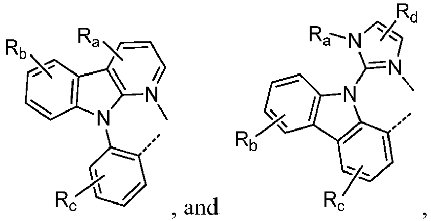
- wherein Ra, Rb, Rc, and Rd may represent mono, di, tri, or tetra substitution, or no substitution;
- wherein Ra, Rb, Rc, and Rd are independently selected from the group consisting of hydrogen, deuterium, halide, alkyl, cycloalkyl, heteroalkyl, arylalkyl, alkoxy, aryloxy, amino, silyl, alkenyl, cycloalkenyl, heteroalkenyl, alkynyl, aryl, heteroaryl, acyl, carbonyl, carboxylic acids, ester, nitrile, isonitrile, sulfanyl, sulfinyl, sulfonyl, phosphino, and combinations thereof; and
- wherein two adjacent substituents of Ra, Rb, Rc, and Rd are optionally joined to form a fused ring or form a multidentate ligand.
- In one embodiment, the first device is a consumer product. In one embodiment, the first device is an organic light-emitting device. In one embodiment, the first device comprises a lighting panel.
- The compounds described in this disclosure were found to have surprising and unexpected properties when used as hosts in the emissive layer and/or blocking materials in PHOLEDs. The inventors discovered bicarbazole compounds with azaDBX having two nitrogents on the same ring showed improved results.
- The materials described herein as useful for a particular layer in an organic light emitting device may be used in combination with a wide variety of other materials present in the device. For example, emissive dopants disclosed herein may be used in conjunction with a wide variety of hosts, transport layers, blocking layers, injection layers, electrodes and other layers that may be present. The materials described or referred to below are non-limiting examples of materials that may be useful in combination with the compounds disclosed herein, and one of skill in the art can readily consult the literature to identify other materials that may be useful in combination.
- A hole injecting/transporting material to be used in the present invention is not particularly limited, and any compound may be used as long as the compound is typically used as a hole injecting/transporting material. Examples of the material include, but not limit to: a phthalocyanine or porphryin derivative; an aromatic amine derivative; an indolocarbazole derivative; a polymer containing fluorohydrocarbon; a polymer with conductivity dopants; a conducting polymer, such as PEDOT/PSS; a self-assembly monomer derived from compounds such as phosphonic acid and sliane derivatives; a metal oxide derivative, such as MoOx; a p-type semiconducting organic compound, such as 1,4,5,8,9,12-Hexaazatriphenylenehexacarbonitrile; a metal complex, and a cross-linkable compounds.
- Examples of aromatic amine derivatives used in HIL or HTL include, but not limit to the following general structures:


- Each of Ar1 to Ar9 is selected from the group consisting aromatic hydrocarbon cyclic compounds such as benzene, biphenyl, triphenyl, triphenylene, naphthalene, anthracene, phenalene, phenanthrene, fluorene, pyrene, chrysene, perylene, azulene; group consisting aromatic heterocyclic compounds such as dibenzothiophene, dibenzofuran, dibenzoselenophene, furan, thiophene, benzofuran, benzothiophene, benzoselenophene, carbazole, indolocarbazole, pyridylindole, pyrrolodipyridine, pyrazole, imidazole, triazole, oxazole, thiazole, oxadiazole, oxatriazole, dioxazole, thiadiazole, pyridine, pyridazine, pyrimidine, pyrazine, triazine, oxazine, oxathiazine, oxadiazine, indole, benzimidazole, indazole, indoxazine, benzoxazole, benzisoxazole, benzothiazole, quinoline, isoquinoline, cinnoline, quinazoline, quinoxaline, naphthyridine, phthalazine, pteridine, xanthene, acridine, phenazine, phenothiazine, phenoxazine, benzofuropyridine, furodipyridine, benzothienopyridine, thienodipyridine, benzoselenophenopyridine, and selenophenodipyridine; and group consisting 2 to 10 cyclic structural units which are groups of the same type or different types selected from the aromatic hydrocarbon cyclic group and the aromatic heterocyclic group and are bonded to each other directly or via at least one of oxygen atom, nitrogen atom, sulfur atom, silicon atom, phosphorus atom, boron atom, chain structural unit and the aliphatic cyclic group. Wherein each Ar is further substituted by a substituent selected from the group consisting of hydrogen, deuterium, halide, alkyl, cycloalkyl, heteroalkyl, arylalkyl, alkoxy, aryloxy, amino, silyl, alkenyl, cycloalkenyl, heteroalkenyl, alkynyl, aryl, heteroaryl, acyl, carbonyl, carboxylic acids, ester, nitrile, isonitrile, sulfanyl, sulfinyl, sulfonyl, phosphino, and combinations thereof.
- In one aspect, Ar1 to Ar9 is independently selected from the group consisting of:


- k is an integer from 1 to 20; X101 to X108 is C (including CH) or N; Z101 is NAr1, O, or S; Ar1 has the same group defined above.
- Examples of metal complexes used in HIL or HTL include, but not limit to the following general formula:

- In one aspect, (Y101-Y102) is a 2-phenylpyridine derivative. In another aspect, (Y101-Y102) is a carbene ligand. In another aspect, Met is selected from Ir, Pt, Os, and Zn. In a further aspect, the metal complex has a smallest oxidation potential in solution vs. Fc+/Fc couple less than about 0.6 V.
- The light emitting layer of the organic EL device of the present invention preferably contains at least a metal complex as light emitting material, and may contain a host material using the metal complex as a dopant material. Examples of the host material are not particularly limited, and any metal complexes or organic compounds may be used as long as the triplet energy of the host is larger than that of the dopant. While the Table below categorizes host materials as preferred for devices that emit various colors, any host material may be used with any dopant so long as the triplet criterion is satisfied.
- Examples of metal complexes used as host are preferred to have the following general formula:

- In one aspect, the metal complexes are:

- In another aspect, Met is selected from Ir and Pt. In a further aspect, (Y103-Y104) is a carbene ligand.
- Examples of organic compounds used as host are selected from the group consisting aromatic hydrocarbon cyclic compounds such as benzene, biphenyl, triphenyl, triphenylene, naphthalene, anthracene, phenalene, phenanthrene, fluorene, pyrene, chrysene, perylene, azulene; group consisting aromatic heterocyclic compounds such as dibenzothiophene, dibenzofuran, dibenzoselenophene, furan, thiophene, benzofuran, benzothiophene, benzoselenophene, carbazole, indolocarbazole, pyridylindole, pyrrolodipyridine, pyrazole, imidazole, triazole, oxazole, thiazole, oxadiazole, oxatriazole, dioxazole, thiadiazole, pyridine, pyridazine, pyrimidine, pyrazine, triazine, oxazine, oxathiazine, oxadiazine, indole, benzimidazole, indazole, indoxazine, benzoxazole, benzisoxazole, benzothiazole, quinoline, isoquinoline, cinnoline, quinazoline, quinoxaline, naphthyridine, phthalazine, pteridine, xanthene, acridine, phenazine, phenothiazine, phenoxazine, benzofuropyridine, furodipyridine, benzothienopyridine, thienodipyridine, benzoselenophenopyridine, and selenophenodipyridine; and group consisting 2 to 10 cyclic structural units which are groups of the same type or different types selected from the aromatic hydrocarbon cyclic group and the aromatic heterocyclic group and are bonded to each other directly or via at least one of oxygen atom, nitrogen atome, sulfur atom, silicon atom, phosphorus atom, boron atom, chain structural unit and the aliphatic cyclic group. Wherein each group is further substituted by a substituent selected from the group consisting of hydrogen, deuterium, halide, alkyl, cycloalkyl, heteroalkyl, arylalkyl, alkoxy, aryloxy, amino, silyl, alkenyl, cycloalkenyl, heteroalkenyl, alkynyl, aryl, heteroaryl, acyl, carbonyl, carboxylic acids, ester, nitrile, isonitrile, sulfanyl, sulfinyl, sulfonyl, phosphino, and combinations thereof.
- In one aspect, host compound contains at least one of the following groups in the molecule:
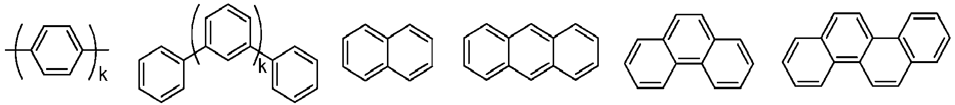

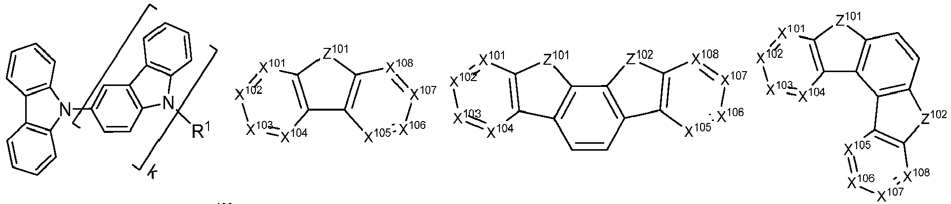

- A hole blocking layer (HBL) may be used to reduce the number of holes and/or excitons that leave the emissive layer. The presence of such a blocking layer in a device may result in substantially higher efficiencies as compared to a similar device lacking a blocking layer. Also, a blocking layer may be used to confine emission to a desired region of an OLED.
- In one aspect, compound used in HBL contains the same molecule or the same functional groups used as host described above.
- In another aspect, compound used in HBL contains at least one of the following groups in the molecule:

- k is an integer from 1 to 20; L101 is an another ligand, k' is an integer from 1 to 3.
- Electron transport layer (ETL) may include a material capable of transporting electrons. Electron transport layer may be intrinsic (undoped), or doped. Doping may be used to enhance conductivity. Examples of the ETL material are not particularly limited, and any metal complexes or organic compounds may be used as long as they are typically used to transport electrons.
- In one aspect, compound used in ETL contains at least one of the following groups in the molecule:


- In another aspect, the metal complexes used in ETL contains, but not limit to the following general formula:

- (O-N) or (N-N) is a bidentate ligand, having metal coordinated to atoms O, N or N, N; L101 is another ligand; k' is an integer value from 1 to the maximum number of ligands that may be attached to the metal.
- In any above-mentioned compounds used in each layer of the OLED device, the hydrogen atoms can be partially or fully deuterated. Thus, any specifically listed substituent, such as, without limitation, methyl, phenyl, pyridyl, etc. encompasses undeuterated, partially deuterated, and fully deuterated versions thereof. Similarly, classes of substituents such as, without limitation, alkyl, aryl, cycloalkyl, heteroaryl, etc. also encompass undeuterated, partially deuterated, and fully deuterated versions thereof.
- In addition to and / or in combination with the materials disclosed herein, many hole injection materials, hole transporting materials, host materials, dopant materials, exiton/hole blocking layer materials, electron transporting and electron injecting materials may be used in an OLED. Non-limiting examples of the materials that may be used in an OLED in combination with materials disclosed herein are listed in Table A below. Table A lists non-limiting classes of materials, non-limiting examples of compounds for each class, and references that disclose the materials.
TABLE A MATERIAL EXAMPLES OF MATERIAL PUBLICATIONS Hole injection materials Phthalocyanine and porphryin compounds 
Appl. Phys. Lett. 69, 2160 (1996) Starburst triarylamines 
J. Lumin. 72-74, 985 (1997) CFX Fluorohydrocarbon polymer 
Appl. Phys. Lett. 78, 673 (2001) Conducting polymers (e.g., PEDOT:PSS, polyaniline, polypthiophene) 
Synth. Met. 87, 171 (1997) WO2007002683 Phosphonic acid and sliane SAMs 
US20030162053 Triarylamine or polythiophene polymers with conductivity dopants 
EP1725079A1 Organic compounds with conductive inorganic compounds, such as molybdenum and tungsten oxides 
US20050123751 SID Symposium Digest, 37, 923 (2006)WO2009018009 n-type semiconducting organic complexes 
US20020158242 Metal organometallic complexes 
US20060240279 Cross-linkable compounds 
US20080220265 Polythiophene based polymers and copolymers 
WO 2011075644 EP2350216 Hole transporting materials Triarylamines (e.g., TPD, α-NPD) 
Appl. Phys. Lett. 51, 913 (1987) 
US5061569 
EP650955 
J. Mater. Chem. 3, 319 (1993) 
Appl. Phys. Lett. 90, 183503 (2007) 
Appl. Phys. Lett. 90, 183503 (2007) Triaylamine on spirofluorene core 
Synth. Met. 91, 209 (1997) Arylamine carbazole compounds 
Adv. Mater. 6, 677 (1994), US20080124572 Triarylamine with (di)benzothiophene/(di)ben zofuran 
US20070278938 ,US20080106190 US20110163302 Indolocarbazoles 
Synth. Met. 111, 421 (2000) Isoindole compounds 
Chem. Mater. 15, 3148 (2003) Metal carbene complexes 
US20080018221 Phosphorescent OLED host materials Red hosts Arylcarbazoles 
Appl. Phys. Lett. 78, 1622 (2001) Metal 8-hydroxyquinolates (e.g., Alq3, BAlq) 
Nature 395, 151 (1998) 
US20060202194 
WO2005014551 
WO2006072002 Metal phenoxybenzothiazole compounds 
Appl. Phys. Lett. 90, 123509 (2007) Conjugated oligomers and polymers (e.g., polyfluorene) 
Org. Electron. 1, 15 (2000) Aromatic fused rings 
WO2009066779 ,WO2009066778 ,WO2009063833 ,US20090045731 ,US20090045730 ,WO2009008311 ,US20090008605 ,US20090009065 Zinc complexes 
WO2010056066 Chrysene based compounds 
WO2011086863 Green hosts Arylcarbazoles 
Appl. Phys. Lett. 78, 1622 (2001) 
US20030175553 
WO2001039234 Aryltriphenylene compounds 
US20060280965 
US20060280965 
WO2009021126 Poly-fused heteroaryl compounds 
US20090309488 US20090302743 US20100012931 Donor acceptor type molecules 
WO2008056746 
WO2010107244 Aza-carbazole/DBT/DBF 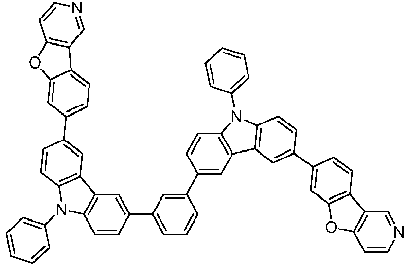
JP2008074939 
US20100187984 Polymers (e.g., PVK) 
Appl. Phys. Lett. 77, 2280(2000) Spirofluorene compounds 
WO2004093207 Metal phenoxybenzooxazole compounds 
WO2005089025 
WO2006132173 
JP200511610 Spirofluorene-carbazole compounds 
JP2007254297 
JP2007254297 Indolocabazoles 
WO2007063796 
WO2007063754 5-member ring electron deficient heterocycles (e.g., triazole, oxadiazole) 
J. Appl. Phys. 90, 5048 (2001) 
WO2004107822 Tetraphenylene complexes 
US20050112407 Metal phenoxypyridine compounds 
WO2005030900 Metal coordination complexes (e.g., Zn, Al with N^N ligands) 
US20040137268 ,US20040137267 Blue hosts Arylcarbazoles 
Appl. Phys. Lett, 82, 2422(2003) 
US20070190359 Dibenzothiophene/Dibenz ofuran-carbazole compounds 
WO2006114966 ,US20090167162 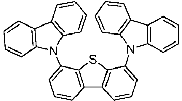
US20090167162 
WO2009086028 
US20090030202 ,US20090017330 
US20100084966 Silicon aryl compounds 
US20050238919 
WO2009003898 Silicon/Germanium aryl compounds 
EP2034538A Aryl benzoyl ester 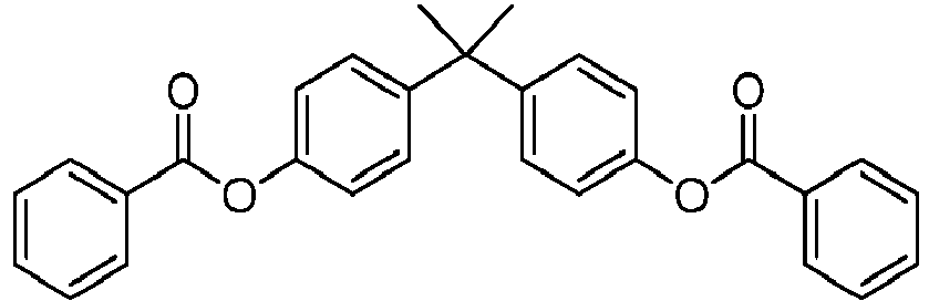
WO2006100298 Carbazole linked by nonconjugated groups 
US20040115476 Aza-carbazoles 
US20060121308 High triplet metal organometallic complex 
US7154114 Phosphorescent dopants Red dopants Heavy metal porphyrins (e.g., PtOEP) 
Nature 395, 151 (1998) Iridium(III) organometallic complexes 
Appl. Phys. Lett. 78, 1622 (2001) 
US2006835469 
US2006835469 
US20060202194 
US20060202194 
US20070087321 
US20080261076 US20100090591 
US20070087321 
Adv. Mater. 19, 739 (2007) 
WO2009100991 
WO2008101842 
US7232618 Platinum(II) organometallic complexes 
WO2003040257 
US20070103060 Osminum(III) complexes 
Chem. Mater. 17, 3532 (2005) Ruthenium(II) complexes 
Adv. Mater. 17, 1059 (2005) Rhenium (I), (II), and (III) complexes 
US20050244673 Green dopants Iridium(III) organometallic complexes 
Inorg. Chem. 40, 1704 (2001) 
US20020034656 
US7332232 
US20090108737 
WO2010028151 
EP1841834B 
US20060127696 
US20090039776 
US6921915 
US20100244004 
US6687266 
Chem. Mater. 16, 2480 (2004) 
US20070190359 
US 20060008670 JP2007123392 
WO2010086089 ,WO2011044988 
Adv. Mater. 16, 2003 (2004) 
Angew. Chem. Int. Ed. 2006,45,7800 
WO2009050290 
US20090165846 
US20080015355 
US20010015432 
US20100295032 Monomer for polymeric metal organometallic compounds 
US7250226 ,US7396598 Pt(II) organometallic complexes, including polydentated ligands 
Appl. Phys. Lett. 86, 153505 (2005) 
Appl. Phys. Lett. 86, 153505 (2005) 
Chem. Lett. 34, 592 (2005) 
WO2002015645 
US20060263635 
US20060182992 US20070103060 Cu complexes 
WO2009000673 
US20070111026 Gold complexes 
Chem. Commun. 2906 (2005) Rhenium(III) complexes 
Inorg. Chem. 42, 1248 (2003) Osmium(II) complexes 
US7279704 Deuterated organometallic complexes 
US20030138657 Organometallic complexes with two or more metal centers 
US20030152802 
US7090928 Blue dopants Iridium(III) organometallic complexes 
WO2002002714 
WO2006009024 
US20060251923 US20110057559 US20110204333 
US7393599 ,WO2006056418 ,US20050260441 ,WO2005019373 
US7534505 
WO2011051404 
US7445855 
US20070190359 ,US20080297033 US20100148663 
US7338722 
US20020134984 
Angew. Chem. Int. Ed. 47, 1 (2008) 
Chem. Mater. 18, 5119 (2006) 
Inorg. Chem. 46, 4308 (2007) 
WO2005123873 
WO2005123873 
WO2007004380 
WO2006082742 Osmium(II) complexes 
US7279704 
Organometallics 23, 3745(2004) Gold complexes 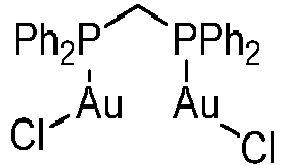
Appl. Phys. Lett.74,1361 (1999) Platinum(II) complexes 
WO2006098120 ,WO2006103874 Pt tetradentate complexes with at least one metal-carbene bond 
US7655323 Exciton/hole blocking layer materials Bathocuprine compounds (e.g., BCP, BPhen) 
Appl. Phys. Lett. 75, 4 (1999) 
Appl. Phys. Lett. 79, 449 (2001) Metal 8-hydroxyquinolates (e.g., BAlq) 
Appl. Phys. Lett. 81, 162(2002) 5-member ring electron deficient heterocycles such as triazole, oxadiazole, imidazole, benzoimidazole 
Appl. Phys. Lett. 81, 162 (2002) Triphenylene compounds 
US20050025993 Fluorinated aromatic compounds 
Appl. Phys. Lett. 79, 156(2001) Phenothiazine-S-oxide 
WO2008132085 Silylated five-membered nitrogen, oxygen, sulfur or phosphorus dibenzoheterocycles 
WO2010079051 Aza-carbazoles 
US20060121308 Electron transporting materials Anthracene-benzoimidazole compounds 
WO2003060956 
US20090179554 Aza triphenylene derivatives 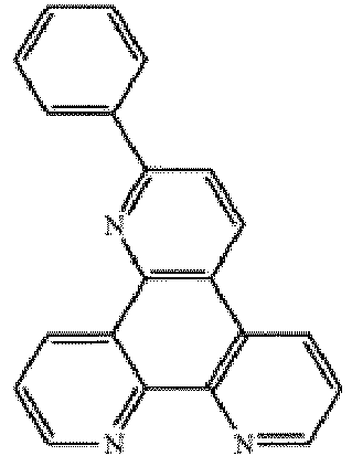
US20090115316 Anthracene-benzothiazole compounds 
Appl. Phys. Lett. 89, 063504 (2006) Metal 8-hydroxyquinolates (e.g., Alq3, Zrq4) 
Appl. Phys. Lett. 51, 913 (1987) US7230107 Metal hydroxybenoquinolates 
Chem. Lett. 5, 905 (1993) Bathocuprine compounds such as BCP, BPhen, etc 
Appl. Phys. Lett. 91, 263503 (2007) 
Appl. Phys. Lett. 79, 449 (2001) 5-member ring electron deficient heterocycles (e.g.,triazole, oxadiazole, imidazole, benzoimidazole) 
Appl. Phys. Lett. 74, 865 (1999) 
Appl. Phys. Lett. 55, 1489(1989) Jpn. J. Apply. Phys. 32, L917 (1993) Silole compounds 
Org. Electron. 4, 113 (2003) Arylborane compounds 
J. Am. Chem. Soc. 120, 9714 (1998) Fluorinated aromatic compounds 
J. Am. Chem. Soc. 122, 1832 (2000) Fullerene (e.g., C60) 
US20090101870 Triazine complexes 
US20040036077 Zn (N^N) complexes 
US6528187 - All reactions were carried out under nitrogen atmosphere unless specified otherwise. All solvents for reactions are anhydrous and used as received from commercial sources. In describing the synthesis of various specific examples of the inventive compound, where X in Formula I is S, the compound is named as Compound "No."-S. For example, Compound 1-S referenced below is Compound 1-X defined above where X is S.
-

- Synthesis of ethyl 3-aminobenzo[b]thiophene-2-carboxylate: A dry 2-neck 500 mL round-bottom flask (RBF) was charged with sodium ethanolate (46.2 mL, 124 mmol), diluted with 151 mL absolute EtOH, cooled in an ice bath and treated dropwise with diethyl malonate (17.98 mL, 118 mmol) under an atmosphere of nitrogen. After stirring for 20 minutes, the ice bath was removed and 3-chlorobenzo[d]isothiazole (20.0 g, 118 mmol) was added in one portion and stirred for 24 hours. The reaction solution was quenched with water, extracted with ether and treated with excess 4 M HCl/dioxane. A pinkish-white precipitate was filtered off, suspended in water, basified with Na2CO3, extracted with ether, washed with water and brine, dried over sodium sulfate, filtered and concentrated to yellow solids (∼20 g) which were recrystallized from ethanol/water and dried in a vacuum oven at 60°C for 3 hrs to give ethyl 3-aminobenzo[b]thiophene-2-carboxylate (19.9 g, 76% yield).

- Synthesis of benzo[4,5]thieno[3,2-d]pyrimidin-4(3H)-one: A 100mL RBF was charged with ethyl 3-aminobenzo[b]thiophene-2-carboxylate (17.7 g, 80 mmol), treated with formamide (60.6 mL, 1520 mmol) and heated to 190 °C for 2 hrs. Precipitate formed upon cooling. The solid was collected by filtration and washed with ether, then recrystallized from ethanol/THF. Benzo[4,5]thieno[3,2-d]pyrimidin-4(3H)-one (9.9 g, 61% yield) was obtained.

- Synthesis of 4-chlorobenzo[4,5]thieno[3,2-d]pyrimidine: Benzo[4,5]thieno[3,2-d]pyrimidin-4(3H)-one (10.78 g, 26.7 mmol) was treated with pyridine (2.68 mL, 33.3 mmol) and phosphoryl trichloride (53.4 mL, 573 mmol), then heated to reflux at 110°C for 1 hr. Excess POCl3 was removed and cautiously quenched with ice water in an ice bath. The pH was adjusted to ∼5 with ammonium hydroxide. Solid was collected by filtration washed with water. The solid was dried to give 4-chlorobenzo[4,5]thieno[3,2-d]pyrimidine (10 g, 85% yield).

- Synthesis of Compound 1-S: 9-phenyl-9H,9'H-3,3'-bicarbazole (3.05 g, 7.47 mmol), 4-chlorobenzo[4,5]thieno[3,2-d]pyrimidine (1.812 g, 8.21 mmol), Pd2dba3 (0.342 g, 0.373 mmol), dicyclohexyl(2',6'-dimethoxy-[1,1'-biphenyl]-2-yl)phosphine (S-Phos) (0.307 g, 0.747 mmol), and sodium 2-methylpropan-2-olate (1.794 g, 18.67 mmol) were charged to a 250 mL RBF, diluted in m-Xylene (Volume: 74.7 mL), degassed with nitrogen and heated to reflux at 150°C overnight. The reaction was quenched with aqueous ammonium chloride and filtered through a plug of Celite® with DCM. The crude was purified by column chromatography and then recrystallized from toluene/ethanol to give 4-(9'-phenyl-9H,9'H-[3,3'-bicarbazol]-9-yl)benzo[4,5]thieno[3,2-d]pyrimidine (1.95 g, 44% yield).
-

- Synthesis of 6-chloro-2-iodopyridin-3-amine: 6-chloropyridin-3-amine (40.0 g, 311 mmol) was dissolved in DMF (Volume: 534 mL) and treated with 1-iodopyrrolidine-2,5-dione (70.0 g, 311 mmol) in one portion. The reaction solution was stirred at room temperature under nitrogen overnight and quenched with water and extracted with EtOAc and Et2O. Organic layer was washed twice with brine and dried over sodium sulfate. DMF was removed on kugelrohr at 100 °C to afford ∼90 g red solids. The crude was purified via column chromatography to give 6-chloro-2-iodopyridin-3-amine (57 g, 72% yield).

- Synthesis of 6-chloro-3'-fluoro-[2,2'-bipyridin]-3-amine: A 3-neck 1000 mL RBF was dried under vacuum, then charged with isopropylmagnesium chloride (78 mL, 156 mmol) and cooled with a water bath. 2-bromo-3-fluoropyridine (14.37 mL, 142 mmol) was added dropwise making sure temperature did not exceed 30 °C. The reaction was stirred at room temperature overnight, then treated dropwise with zinc(II) chloride (341 mL, 170 mmol) over 3 hrs and stirred at room temperature overnight. This suspension was then added dropwise via canula to a degassed, 65 °C solution of Pd(PPh3)4 (8.21 g, 7.10 mmol) and 6-chloro-2-iodopyridin-3-amine (39.8 g, 156 mmol) in THF (Volume: 474 mL) and heated at reflux overnight. After cooled to room temperature, the reaction was quenched with sat. aq. NaHCO3 and water. The precipitate was filtered out and washed with EtOAc. The filtrate was extracted with EtOAc. The crude product was purified by column chromatography in 40-50% EtOAc/hexanes with column conditioned in 20% TEA/hexanes to give 6-chloro-3'-fluoro-[2,2'-bipyridin]-3-amine (21.8 g, 69% yield).

- Synthesis of 6-chloro-3'-fluoro-3-iodo-2,2'-bipyridine: A 500 mL 3 neck RBF equipped with mechanical stirrer, reflux condenser, and addition funnel was charged with 6-chloro-3'-fluoro-[2,2'-bipyridin]-3-amine (6.63 g, 29.6 mmol). It was treated with 2 M sulfuric acid (111 mL, 222 mmol) creating a yellow/orange solution. The reaction was cooled to -5 °C and treated dropwise with a solution of sodium nitrite (2.66 g, 38.5 mmol) in 49 mL water at - 5 °C. The yellow/orange suspension was stirred at 0 °C for 30 minutes, then treated dropwise with a solution of potassium iodide (14.76 g, 89 mmol) in 63 mL of water. The reaction was stirred at room temperature for 30 minutes, then heated to 80°C for 1 hour. After cooling, the reaction was extracted with EtOAc, washed with water, 2M Na2CO3, NaHSO3, and brine, dried over sodium sulfate, filtered, and concentrated. The crude product was purified by column chromatography using 20% EtOAc/hexanes to give 6-chloro-3'-fluoro-3-iodo-2,2'-bipyridine (16 g, 81 % yield).

- Synthesis of ethyl 3-((6-chloro-3'-fluoro-[2,2'-bipyridin]-3-yl)thio)propanoate. 6-chloro-3'-fluoro-3-iodo-2,2'-bipyridine (21.4 g, 64.0 mmol), Potassium Carbonate (22.10 g, 160 mmol), (oxybis(2,1-phenylene))bis(diphenylphosphine) (3.45 g, 6.40 mmol), Pd2(dba)3 (2.93 g, 3.20 mmol) were charged to a dry 500 mL RBF, taken up in Toluene (Volume: 256 mL) and degassed with nitrogen. Ethyl 3-mercaptopropanoate (8.92 mL, 70.4 mmol) was added and the reaction solution was heated to reflux for 7 hours. The reaction was quenched with NH4Cl and extracted with EtOAc. The crude was purified by column chromatography using EtOAc and hexanes to give ethyl 3-((6-chloro-3'-fluoro-[2,2'-bipyridin]-3-yl)thio)propanoate (21.5 g, ∼100% yield) with some impurities.

- Synthesis of 2-chlorothieno[3,2-b:4,5-b']dipyridine: A 500mL RBF was charged with ethyl 3-((6-chloro-3'-fluoro-[2,2'-bipyridin]-3-yl)thio)propanoate (16.55 g, 48.6 mmol), THF (Volume: 194 ml) and degassed with nitrogen for 10 minutes, then treated with potassium 2-methylpropan-2-olate (8.17 g, 72.8 mmol) and heated to reflux at 75°C for 24 hours. The reaction was quenched with aqueous ammonium chloride, extracted 2x with EtOAc. The crude product was purified by column chromatography to give 2-chlorothieno[3,2-b:4,5-b']dipyridine (7 g, 68% yield).

- Synthesis of Compound D: 9-phenyl-9H,9'H-3,3'-bicarbazole (3.0 g, 7.34 mmol), 2-chlorothieno[3,2-b:4,5-b']dipyridine (2.026 g, 9.18 mmol), Pd2dba3 (0.336 g, 0.367 mmol), dicyclohexyl(2',6'-dimethoxy-[1,1'-biphenyl]-2-yl)phosphine (S-Phos) (0.301 g, 0.734 mmol), and sodium 2-methylpropan-2-olate (1.764 g, 18.36 mmol) were charged to a dry 250 mL RBF, treated with m-Xylene (Volume: 73.4 mL) and degassed with nitrogen then heated to reflux at 150 °C overnight. The reaction solution was cooled to room temperature, quenched with aq. NH4Cl and filtered through small plug of Celite® with dichloromethane (DCM). The rude product was purified by column chromatography to give 1.86 g pure product.
- All devices were fabricated by high vacuum (∼ 10-7 Torr) thermal evaporation. The anode electrode was 120 nm of indium tin oxide (ITO). The cathode consisted of 1 nm of LiF followed by 100 nm of Aluminum. All devices were encapsulated with a glass lid sealed with an epoxy resin in a nitrogen glove box 1 ppm of H2O and O2) immediately after fabrication, and a moisture getter was incorporated inside the package. All device examples had organic stacks consisting of, sequentially, from the ITO surface, 10 nm thick of Compound A as the hole injection layer (HIL), 30 nm of 4,4'-bis[N-(1-naphthyl)-N-phenylaminolbiphenyl (α-NPD), as the hole transporting layer (HTL), and 300 Å of inventive hosts or comparative hosts doped with 10 wt% of Compound A as the emissive layer (EML). On the top of the EML, 5 nm of Compound B was deposited as a hole blocking (BL) and then followed by 45 nm of tris(8-hydroxyquino1inato)aluminum (Alq3) as the ETL.
- Material used in the devices:

Table 2. Device structures of inventive compounds and comparative compounds Example HIL HTL EML (300 Å, doping %) BL ETL Inventive Example 1 Compound A 100Å NPD 300Å Compound B: Compound 1-S (73:20) Compound A Compound B 50Å Alq 450Å 7% Inventive Example 2 Compound A 100Å NPD 300Å Compound 1-S (90%) Compound A Compound B 50Å Alq 450Å 10% Comparative Example 1 Compound A 100Å NPD 300Å Compound B: Compound C (73:20) Compound A Compound B 50Å Alq 450Å 7% Comparative Example 2 Compound A 100Å NPD 300Å Compound B: Compound D (73:20) Compound A Compound B 50Å Alq 450Å 7% Comparative Example 3 Compound A 100Å NPD 300Å Compound C (90%) Compound A Compound B 50Å Alq 450Å 10% Comparative Example 4 Compound A 100Å NPD 300Å Compound D (90%) Compound A Compound B 50Å Alq 450Å 10% Table 3. Device results x y λmax (nm) Relative Voltage Relative EQE Relative LT95 from 9000 nits Inventive Example 1 0.343 0.612 524 1.03 1.2 1.54 Comparative Example 1 0.338 0.615 524 1.0 1.1 0.7 Comparative Example 2 0.335 0.617 522 1.0 1.0 1.0 Table 4. Device results x y λmax (nm) Relative Voltage Relative EQE Relative LT95 from 9000 nits Inventive Example 2 0.347 0.611 526 0.86 2.0 9.33 Comparative Example 3 0.345 0.612 526 0.86 1.76 1.0 Comparative Example 4 0.347 0.605 526 1.0 1.0 1.0 - Table 3 above summarizes the performance of the devices with dual hosts containing Compound B and inventive compound Compound 1-S or Compounds C and D. Table 4 above summarizes the performance of the devices with single host inventive compound Compound 1-S or Compounds C and D. The driving voltage, and external quantum efficiency (EQE) were measured at 1000 nits, while the lifetime (LT95) was defined as the time required for the device to decay to 95% of its initial luminance of 9000 nits. All devices have essentially same emission color, which is from the emission of Compound A. Device with inventive Compound 1-S as host shows much improved performance compared to the comparative examples. When used as a cohost with Compound B, inventive Compound 1-S showed similar driving voltage and slightly improved efficiency compared to that of Compounds C and D. However, the device lifetime was improved by 50% compared to Compound D, and more than doubled compared to Compound C. When used as a single host, inventive Compound 1-S showed much lower voltage than that of Compound D, much higher efficiency than both Compounds C and D. More importantly, the device lifetime with Compound 1-S is more than 9 times better than that of Compounds C and D. These results have clearly demonstrated the unexpected advantages of using the current invented compounds in OLED device.
- It is understood that the various embodiments described herein are by way of example only, and are not intended to limit the scope of the invention. For example, many of the materials and structures described herein may be substituted with other materials and structures without deviating from the spirit of the invention. The present invention as claimed may therefore include variations from the particular examples and preferred embodiments described herein, as will be apparent to one of skill in the art. It is understood that various theories as to why the invention works are not intended to be limiting.
Claims (21)
- A compound having a structure according to Formula I
 wherein R2, R5, and R6 represent mono, di, tri, tetra substitutions or no substitution;wherein R3, and R4 represent mono, di, tri substitutions or no substitution;wherein L is a single bond or comprises an aryl or heteroaryl group having from 3-24 carbon atoms, which is optionally further substituted with one or more groups selected from hydrogen, deuterium, alkyl, cycloalkyl, aralkyl, alkoxy, aryloxy, amino, silyl, aryl, heteroaryl, and combinations thereof;wherein X is selected from the group consisting of O, S, and Se;wherein each of Y1, Y2, Y3, and Y4 is carbon or nitrogen;wherein at least two of Y1, Y2, Y3, and Y4 are nitrogen;wherein at least one of Y1, Y2, Y3, and Y4 is carbon and bonded to L; andwherein R1, R2, R3, R4, R5 and R6 are each independently selected from the group consisting of hydrogen, deuterium, halide, alkyl, cycloalkyl, heteroalkyl, arylalkyl, alkoxy, aryloxy, amino, silyl, alkenyl, cycloalkenyl, heteroalkenyl, alkynyl, aryl, heteroaryl, acyl, carbonyl, carboxylic acids, ester, nitrile, isonitrile, sulfanyl, sulfinyl, sulfonyl, phosphino, and combinations thereof.
 - The compound of Claim 1, wherein R1 is aryl or heteroaryl.
- The compound of Claim 1, wherein R1 is selected from the group consisting of phenyl, biphenyl, terphenyl, tetraphenyl, pentaphenyl, pyridine, phenyl pyridine, pyridyl phenyl, triphenylene, carbazole, fluorene, dibenzofuran, dibenzothiophene, dibenzoselenophene and combinations thereof.
- The compound of Claim 1, wherein R2, R3, R4, R5 and R6 are each independently selected from the group consisting of hydrogen, deuterium, aryl, heteroaryl and combinations thereof.
- The compound of Claim 1, wherein R2, R3, R4, R5 and R6 are each independently selected from the group consisting of hydrogen, deuterium, phenyl, biphenyl, terphenyl, tetraphenyl, pentaphenyl, pyridine, phenyl pyridine, pyridyl phenyl, triphenylene, carbazole, fluorene, dibenzofuran, dibenzothiophene, dibenzoselenophene and combinations thereof..
- The compound of Claim1, wherein R2, R3, R4, R5 and R6 are hydrogen.
- The compound of Claim1, wherein L is selected from the group consisting of:


- The compound of Claim1, wherein X is O.
- The compound of Claim1, wherein X is S.
- The compound of Claim 1, wherein the compound is selected from the group consisting of:


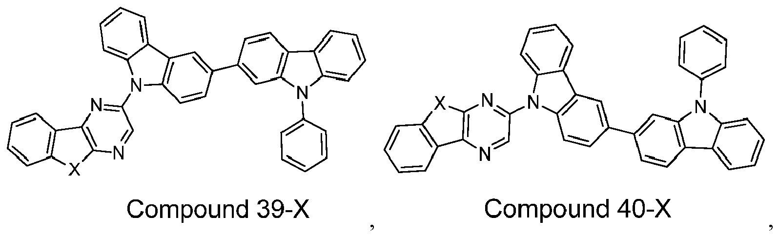


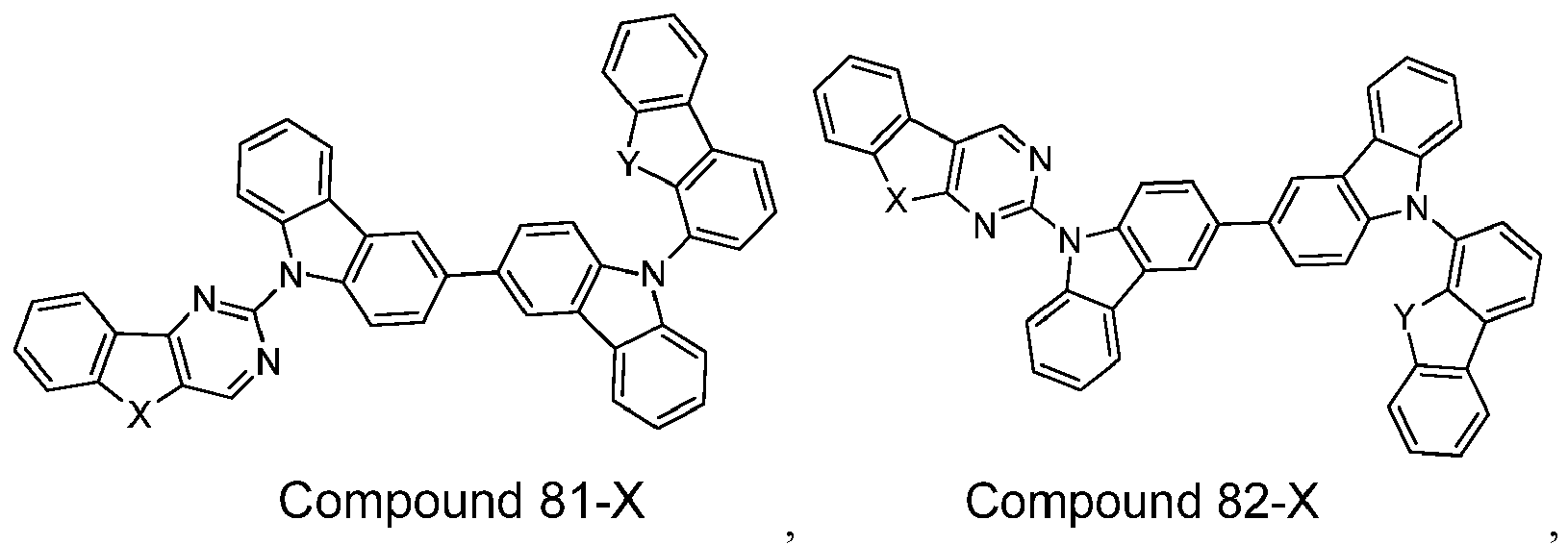


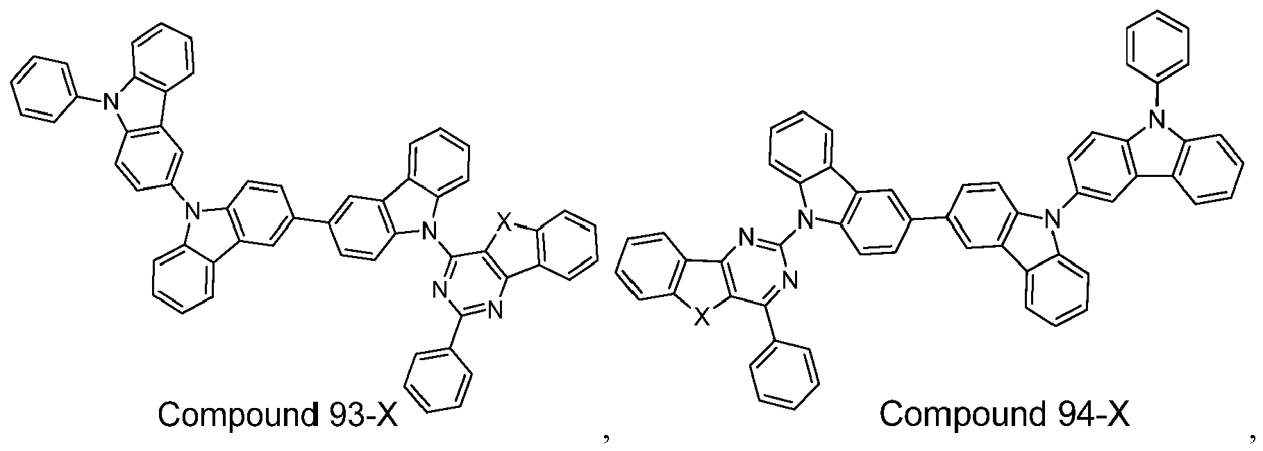


- A first device comprising an organic light emitting device, the organic light emitting device comprising:an anode;a cathode;an organic layer, disposed between the anode and the cathode, wherein the organic layer comprises a compound having a structure according to Formula I
 wherein R2, R5, and R6 represent mono, di, tri, tetra substitutions or no substitution;wherein R3, and R4 represent mono, di, tri substitutions or no substitution;wherein L is a single bond or comprises an aryl or heteroaryl group having from 3-24 carbon atoms, which is optionally further substituted with one or more groups selected from hydrogen, deuterium, alkyl, cycloalkyl, aralkyl, alkoxy, aryloxy, amino, silyl, aryl, heteroaryl, and combinations thereof;wherein X is selected from the group consisting of O, S, and Se;wherein each of Y1, Y2, Y3, and Y4 is carbon or nitrogen;wherein at least two of Y1, Y2, Y3, and Y4 are nitrogen;wherein at least one of Y1, Y2, Y3, and Y4 is carbon and bonded to L; andwherein R1, R2, R3, R4, R5 and R6 are each independently selected from the group consisting of hydrogen, deuterium, halide, alkyl, cycloalkyl, heteroalkyl, arylalkyl, alkoxy, aryloxy, amino, silyl, alkenyl, cycloalkenyl, heteroalkenyl, alkynyl, aryl, heteroaryl, acyl, carbonyl, carboxylic acids, ester, nitrile, isonitrile, sulfanyl, sulfinyl, sulfonyl, phosphino, and combinations thereof.
 - The first device of Claim 11, wherein the compound is selected from the group consisting of:


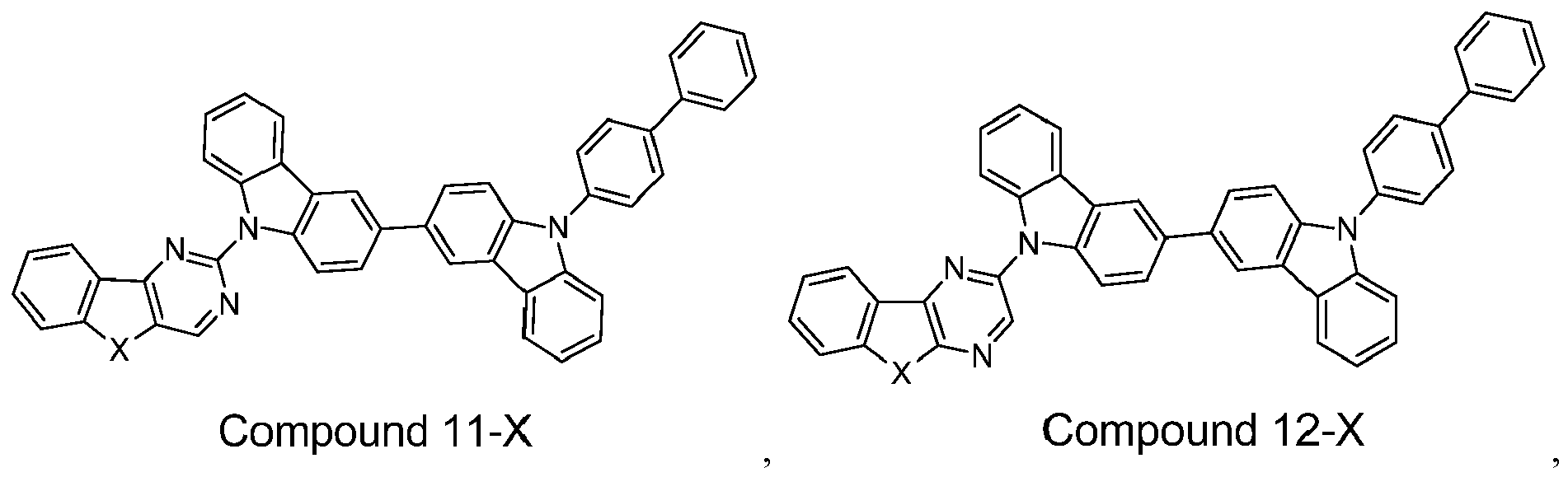


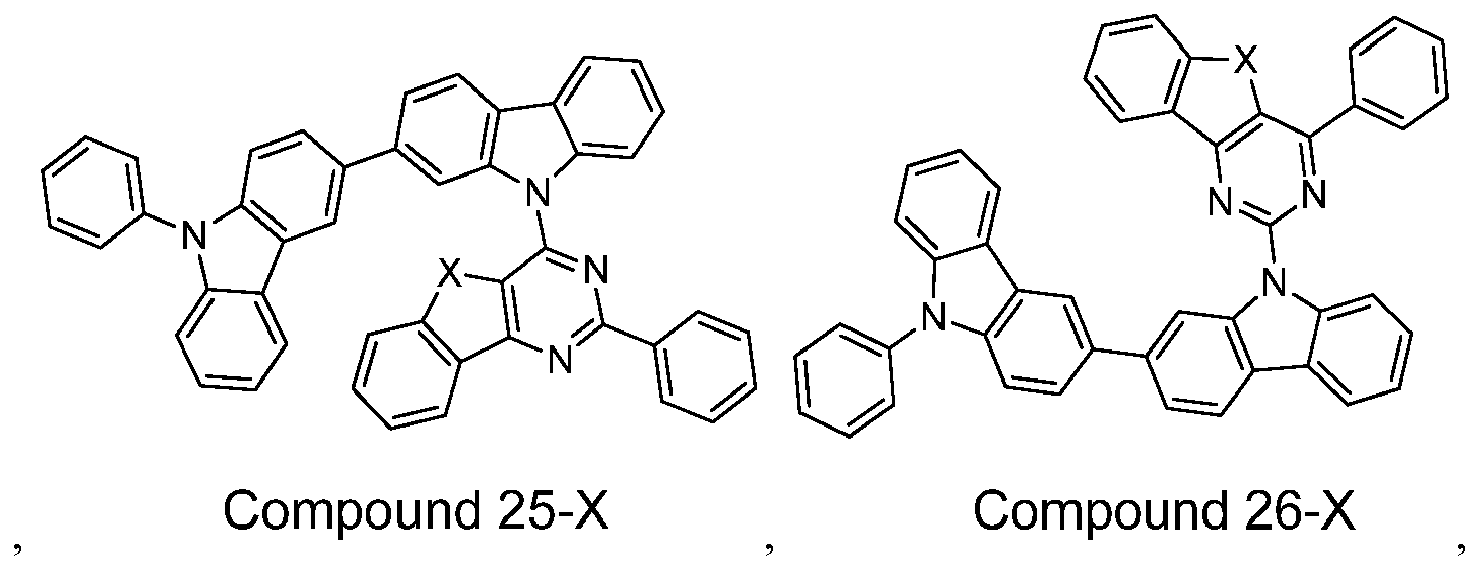


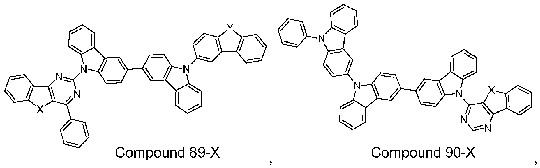


- The first device of Claim 11, wherein the organic layer is an emissive layer and the compound having Formula I is a host.
- The first device of Claim 13, wherein the organic layer further comprises an emissive dopant.
- The first device of Claim 14, wherein the emissive dopant is a transition metal complex having at least one ligand selected from the group consisting of:


 wherein Ra, Rb, Rc, and Rd may represent mono, di, tri, or tetra substitution, or no substitution;wherein Ra, Rb, Rc, and Rd are independently selected from the group consisting of hydrogen, deuterium, halide, alkyl, cycloalkyl, heteroalkyl, arylalkyl, alkoxy, aryloxy, amino, silyl, alkenyl, cycloalkenyl, heteroalkenyl, alkynyl, aryl, heteroaryl, acyl, carbonyl, carboxylic acids, ester, nitrile, isonitrile, sulfanyl, sulfinyl, sulfonyl, phosphino, and combinations thereof; andwherein two adjacent substituents of Ra, Rb, Rc, and Rd are optionally joined to form a fused ring or form a multidentate ligand.
 - The first device of Claim 11, wherein the organic layer is a blocking layer and the compound having Formula I is a blocking material in the organic layer.
- The first device of Claim 11, wherein the organic layer is an electron transporting and the compound having Formula I is an electron transporting material in the organic layer.
- The first device of Claim 11, wherein the first device is a consumer product.
- The first device of Claim 11, wherein the first device is an organic light-emitting device.
- The first device of Claim 11, wherein the first device comprises a lighting panel.
- A a formulation comprising a compound having a structure according to Formula I
 wherein R2, R5, and R6 represent mono, di, tri, tetra substitutions or no substitution;wherein R3, and R4 represent mono, di, tri substitutions or no substitution;wherein L is a single bond or comprises an aryl or heteroaryl group having from 3-24 carbon atoms, which is optionally further substituted with one or more groups selected from hydrogen, deuterium, alkyl, cycloalkyl, aralkyl, alkoxy, aryloxy, amino, silyl, aryl, heteroaryl, and combinations thereof;wherein X is selected from the group consisting of O, S, and Se;wherein each of Y1, Y2, Y3, and Y4 is carbon or nitrogen;wherein at least two of Y1, Y2, Y3, and Y4 are nitrogen;wherein at least one of Y1, Y2, Y3, and Y4 is carbon and bonded to L; andwherein R1, R2, R3, R4, R5 and R6 are each independently selected from the group consisting of hydrogen, deuterium, halide, alkyl, cycloalkyl, heteroalkyl, arylalkyl, alkoxy, aryloxy, amino, silyl, alkenyl, cycloalkenyl, heteroalkenyl, alkynyl, aryl, heteroaryl, acyl, carbonyl, carboxylic acids, ester, nitrile, isonitrile, sulfanyl, sulfinyl, sulfonyl, phosphino, and combinations thereof.
Applications Claiming Priority (1)
| Application Number | Priority Date | Filing Date | Title |
|---|---|---|---|
| US13/942,921 US9553274B2 (en) | 2013-07-16 | 2013-07-16 | Organic electroluminescent materials and devices |
Publications (2)
| Publication Number | Publication Date |
|---|---|
| EP2826781A1 true EP2826781A1 (en) | 2015-01-21 |
| EP2826781B1 EP2826781B1 (en) | 2016-05-11 |
Family
ID=51167786
Family Applications (1)
| Application Number | Title | Priority Date | Filing Date |
|---|---|---|---|
| EP14176868.9A Active EP2826781B1 (en) | 2013-07-16 | 2014-07-14 | Bicarbazole containing compounds for OLED |
Country Status (5)
| Country | Link |
|---|---|
| US (1) | US9553274B2 (en) |
| EP (1) | EP2826781B1 (en) |
| JP (3) | JP6681136B2 (en) |
| KR (1) | KR102236224B1 (en) |
| CN (1) | CN104292241B (en) |
Cited By (8)
| Publication number | Priority date | Publication date | Assignee | Title |
|---|---|---|---|---|
| EP2910555A1 (en) * | 2014-02-24 | 2015-08-26 | Universal Display Corporation | Organic electroluminescent materials and devices |
| EP3109231A1 (en) * | 2015-06-23 | 2016-12-28 | Samsung Electronics Co., Ltd. | Carbazole compound and organic light-emitting device including the same |
| US20180114920A1 (en) * | 2016-10-24 | 2018-04-26 | Novaled Gmbh | Electron Transport Layer Stack for an Organic Light-Emitting Diode |
| US10230055B2 (en) | 2015-09-04 | 2019-03-12 | Semiconductor Energy Laboratory Co., Ltd. | Compound, light-emitting element, display device, electronic device, and lighting device |
| US10868258B2 (en) | 2016-12-23 | 2020-12-15 | Semiconductor Energy Laboratory Co., Ltd. | Organic compound, light-emitting element, light-emitting device, electronic device, and lighting device |
| US11279719B2 (en) | 2017-01-26 | 2022-03-22 | Youla S. Tsantrizos | Substituted bicyclic pyrimidine-based compounds and compositions and uses thereof |
| US11456424B2 (en) | 2017-06-23 | 2022-09-27 | Semiconductor Energy Laboratory Co., Ltd. | Phosphorescent host material |
| WO2023078812A1 (en) | 2021-11-02 | 2023-05-11 | Merck Patent Gmbh | Benzofuro[3,2-d]pyrimidino-2,4-dicarbonitril derivatives and similar compounds for organic electroluminescence devices |
Families Citing this family (30)
| Publication number | Priority date | Publication date | Assignee | Title |
|---|---|---|---|---|
| US9324949B2 (en) * | 2013-07-16 | 2016-04-26 | Universal Display Corporation | Organic electroluminescent materials and devices |
| JP6507534B2 (en) * | 2013-09-11 | 2019-05-08 | 東ソー株式会社 | Benzothienopyrimidine compound, method for producing the same, and organic electroluminescent device containing the same |
| CN106414452B (en) * | 2014-03-10 | 2019-10-11 | 三星Sdi株式会社 | It is condensed cyclic compound and the organic light emitting apparatus containing it |
| KR20160007380A (en) * | 2014-07-11 | 2016-01-20 | 가부시키가이샤 한도오따이 에네루기 켄큐쇼 | Light-emitting element, compound, display module, lighting module, light-emitting device, display device, lighting device, and electronic device |
| CN115572284A (en) * | 2014-09-25 | 2023-01-06 | 三星显示有限公司 | Crosslinkable host material |
| KR101842584B1 (en) * | 2015-02-13 | 2018-03-27 | 삼성에스디아이 주식회사 | Organic compound for optoelectric device and organic optoelectric device and display device |
| JPWO2016129694A1 (en) * | 2015-02-13 | 2017-11-24 | 出光興産株式会社 | COMPOUND, MATERIAL FOR ORGANIC ELECTROLUMINESCENT DEVICE, INK COMPOSITION, ORGANIC ELECTROLUMINESCENT DEVICE, AND ELECTRONIC DEVICE |
| JP6840931B2 (en) * | 2015-03-09 | 2021-03-10 | 東ソー株式会社 | Method for Producing Fused Ring Aromatic Compound |
| US11495749B2 (en) | 2015-04-06 | 2022-11-08 | Universal Display Corporation | Organic electroluminescent materials and devices |
| US20160293855A1 (en) | 2015-04-06 | 2016-10-06 | Universal Display Corporation | Organic Electroluminescent Materials and Devices |
| US11818949B2 (en) | 2015-04-06 | 2023-11-14 | Universal Display Corporation | Organic electroluminescent materials and devices |
| TWI757234B (en) * | 2015-05-21 | 2022-03-11 | 日商半導體能源研究所股份有限公司 | Light-emitting element, display device, electronic device, and lighting device |
| KR101897041B1 (en) | 2015-05-22 | 2018-09-10 | 삼성에스디아이 주식회사 | Compound for organic optoelectric device, composition for optoelectric device, organic optoelectric device and display device |
| CN110600635A (en) * | 2015-05-29 | 2019-12-20 | 株式会社半导体能源研究所 | Light-emitting element, light-emitting device, display device, electronic device, and lighting device |
| DE112016003078T5 (en) * | 2015-07-08 | 2018-04-26 | Semiconductor Energy Laboratory Co., Ltd. | Light emitting element, display device, electronic device and lighting device |
| CN111341927B (en) * | 2015-09-30 | 2023-06-09 | 株式会社半导体能源研究所 | Light emitting element, display device, electronic device, and lighting device |
| KR102453744B1 (en) * | 2015-10-21 | 2022-10-11 | 삼성전자주식회사 | Intermediate for Heteroacene Compound and Method of Synthesizing Heteroacene Compound Using the Intermediate |
| WO2017109637A1 (en) | 2015-12-25 | 2017-06-29 | Semiconductor Energy Laboratory Co., Ltd. | Compound, light-emitting element, display device, electronic device, and lighting device |
| JP6788314B2 (en) * | 2016-01-06 | 2020-11-25 | コニカミノルタ株式会社 | Organic electroluminescence element, manufacturing method of organic electroluminescence element, display device and lighting device |
| CN105884786B (en) * | 2016-05-13 | 2018-08-31 | 苏州大学 | Benzofuran [2,3-b] pyrazines derivatives and its application in organic electroluminescence fluorescent device |
| KR20180032354A (en) * | 2016-09-22 | 2018-03-30 | 삼성전자주식회사 | Condensed cyclic compound and organic light emitting device including the same |
| US11264576B2 (en) * | 2016-12-19 | 2022-03-01 | Idemitsu Kosan Co., Ltd. | Specifically substituted ladder type compounds for organic light emitting devices |
| CN110073510B (en) * | 2016-12-28 | 2022-07-19 | 株式会社半导体能源研究所 | Light-emitting element, organic compound, light-emitting device, electronic device, and lighting device |
| KR102630642B1 (en) * | 2018-02-09 | 2024-01-30 | 삼성디스플레이 주식회사 | Heterocyclic compound and organic light emitting device comprising the same |
| US20210313520A1 (en) * | 2018-08-03 | 2021-10-07 | Semiconductor Energy Laboratory Co., Ltd. | Light-Emitting Device, Light-Emitting Apparatus, Electronic Device, and Lighting Device |
| US20210371427A1 (en) * | 2018-10-19 | 2021-12-02 | Semiconductor Energy Laboratory Co., Ltd. | Organic Compound, Light-Emitting Device Material, Light-Emitting Device, Light-Emitting Apparatus, Light-Emitting Module, Electronic Device, and Lighting Device |
| US11834459B2 (en) | 2018-12-12 | 2023-12-05 | Universal Display Corporation | Host materials for electroluminescent devices |
| JPWO2020208475A1 (en) * | 2019-04-12 | 2020-10-15 | ||
| CN115103845A (en) * | 2020-02-14 | 2022-09-23 | 株式会社半导体能源研究所 | Organic compound, light-emitting device, electronic apparatus, light-emitting device, and lighting device |
| WO2023061998A1 (en) | 2021-10-14 | 2023-04-20 | Merck Patent Gmbh | Materials for organic electroluminescent devices |
Citations (20)
| Publication number | Priority date | Publication date | Assignee | Title |
|---|---|---|---|---|
| US4769292A (en) | 1987-03-02 | 1988-09-06 | Eastman Kodak Company | Electroluminescent device with modified thin film luminescent zone |
| US5247190A (en) | 1989-04-20 | 1993-09-21 | Cambridge Research And Innovation Limited | Electroluminescent devices |
| US5703436A (en) | 1994-12-13 | 1997-12-30 | The Trustees Of Princeton University | Transparent contacts for organic devices |
| US5707745A (en) | 1994-12-13 | 1998-01-13 | The Trustees Of Princeton University | Multicolor organic light emitting devices |
| US5834893A (en) | 1996-12-23 | 1998-11-10 | The Trustees Of Princeton University | High efficiency organic light emitting devices with light directing structures |
| US5844363A (en) | 1997-01-23 | 1998-12-01 | The Trustees Of Princeton Univ. | Vacuum deposited, non-polymeric flexible organic light emitting devices |
| US6013982A (en) | 1996-12-23 | 2000-01-11 | The Trustees Of Princeton University | Multicolor display devices |
| US6087196A (en) | 1998-01-30 | 2000-07-11 | The Trustees Of Princeton University | Fabrication of organic semiconductor devices using ink jet printing |
| US6091195A (en) | 1997-02-03 | 2000-07-18 | The Trustees Of Princeton University | Displays having mesa pixel configuration |
| US6097147A (en) | 1998-09-14 | 2000-08-01 | The Trustees Of Princeton University | Structure for high efficiency electroluminescent device |
| US6294398B1 (en) | 1999-11-23 | 2001-09-25 | The Trustees Of Princeton University | Method for patterning devices |
| US6303238B1 (en) | 1997-12-01 | 2001-10-16 | The Trustees Of Princeton University | OLEDs doped with phosphorescent compounds |
| US6337102B1 (en) | 1997-11-17 | 2002-01-08 | The Trustees Of Princeton University | Low pressure vapor phase deposition of organic thin films |
| US20030230980A1 (en) | 2002-06-18 | 2003-12-18 | Forrest Stephen R | Very low voltage, high efficiency phosphorescent oled in a p-i-n structure |
| US20040174116A1 (en) | 2001-08-20 | 2004-09-09 | Lu Min-Hao Michael | Transparent electrodes |
| US7279704B2 (en) | 2004-05-18 | 2007-10-09 | The University Of Southern California | Complexes with tridentate ligands |
| US7431968B1 (en) | 2001-09-04 | 2008-10-07 | The Trustees Of Princeton University | Process and apparatus for organic vapor jet deposition |
| US7968146B2 (en) | 2006-11-01 | 2011-06-28 | The Trustees Of Princeton University | Hybrid layers for use in coatings on electronic devices or other articles |
| WO2011137072A1 (en) * | 2010-04-26 | 2011-11-03 | Universal Display Corporation | Bicarbazole containing compounds for oleds |
| EP2762477A1 (en) * | 2011-09-28 | 2014-08-06 | Idemitsu Kosan Co., Ltd | Material for organic electroluminescent element, and organic electroluminescent element produced using same |
Family Cites Families (115)
| Publication number | Priority date | Publication date | Assignee | Title |
|---|---|---|---|---|
| US5061569A (en) | 1990-07-26 | 1991-10-29 | Eastman Kodak Company | Electroluminescent device with organic electroluminescent medium |
| DE69412567T2 (en) | 1993-11-01 | 1999-02-04 | Hodogaya Chemical Co Ltd | Amine compound and electroluminescent device containing it |
| JP3139321B2 (en) | 1994-03-31 | 2001-02-26 | 東レ株式会社 | Light emitting element |
| US6528187B1 (en) | 1998-09-08 | 2003-03-04 | Fuji Photo Film Co., Ltd. | Material for luminescence element and luminescence element using the same |
| US6830828B2 (en) | 1998-09-14 | 2004-12-14 | The Trustees Of Princeton University | Organometallic complexes as phosphorescent emitters in organic LEDs |
| US6458475B1 (en) | 1999-11-24 | 2002-10-01 | The Trustee Of Princeton University | Organic light emitting diode having a blue phosphorescent molecule as an emitter |
| KR100377321B1 (en) | 1999-12-31 | 2003-03-26 | 주식회사 엘지화학 | Electronic device comprising organic compound having p-type semiconducting characteristics |
| KR100346984B1 (en) | 2000-02-08 | 2002-07-31 | 삼성에스디아이 주식회사 | Hole Transporting Compound Having Good Thermal Stability for Organic Electroluminescent Devices and Method for the Same |
| US20020121638A1 (en) | 2000-06-30 | 2002-09-05 | Vladimir Grushin | Electroluminescent iridium compounds with fluorinated phenylpyridines, phenylpyrimidines, and phenylquinolines and devices made with such compounds |
| AU2001283274A1 (en) | 2000-08-11 | 2002-02-25 | The Trustees Of Princeton University | Organometallic compounds and emission-shifting organic electrophosphorescence |
| US6579630B2 (en) | 2000-12-07 | 2003-06-17 | Canon Kabushiki Kaisha | Deuterated semiconducting organic compounds used for opto-electronic devices |
| JP3812730B2 (en) | 2001-02-01 | 2006-08-23 | 富士写真フイルム株式会社 | Transition metal complex and light emitting device |
| JP4307000B2 (en) | 2001-03-08 | 2009-08-05 | キヤノン株式会社 | Metal coordination compound, electroluminescent element and display device |
| JP4310077B2 (en) | 2001-06-19 | 2009-08-05 | キヤノン株式会社 | Metal coordination compound and organic light emitting device |
| AU2002345362A1 (en) | 2001-06-20 | 2003-01-08 | Showa Denko K.K. | Light emitting material and organic light-emitting device |
| US7250226B2 (en) | 2001-08-31 | 2007-07-31 | Nippon Hoso Kyokai | Phosphorescent compound, a phosphorescent composition and an organic light-emitting device |
| US6835469B2 (en) | 2001-10-17 | 2004-12-28 | The University Of Southern California | Phosphorescent compounds and devices comprising the same |
| US7166368B2 (en) | 2001-11-07 | 2007-01-23 | E. I. Du Pont De Nemours And Company | Electroluminescent platinum compounds and devices made with such compounds |
| US6863997B2 (en) | 2001-12-28 | 2005-03-08 | The Trustees Of Princeton University | White light emitting OLEDs from combined monomer and aggregate emission |
| KR100691543B1 (en) | 2002-01-18 | 2007-03-09 | 주식회사 엘지화학 | New material for transporting electron and organic electroluminescent display using the same |
| US6878975B2 (en) | 2002-02-08 | 2005-04-12 | Agilent Technologies, Inc. | Polarization field enhanced tunnel structures |
| US7189989B2 (en) | 2002-08-22 | 2007-03-13 | Fuji Photo Film Co., Ltd. | Light emitting element |
| AU2003261758A1 (en) | 2002-08-27 | 2004-03-19 | Fujitsu Limited | Organometallic complexes, organic el devices, and organic el displays |
| US6687266B1 (en) | 2002-11-08 | 2004-02-03 | Universal Display Corporation | Organic light emitting materials and devices |
| JP4365199B2 (en) | 2002-12-27 | 2009-11-18 | 富士フイルム株式会社 | Organic electroluminescence device |
| JP4365196B2 (en) | 2002-12-27 | 2009-11-18 | 富士フイルム株式会社 | Organic electroluminescence device |
| EP2062908B1 (en) | 2003-03-24 | 2016-07-13 | University of Southern California | Transition metal complexes comprising pyrazolylcarbazole ligands |
| US7090928B2 (en) | 2003-04-01 | 2006-08-15 | The University Of Southern California | Binuclear compounds |
| US7345301B2 (en) | 2003-04-15 | 2008-03-18 | Merck Patent Gmbh | Mixtures of matrix materials and organic semiconductors capable of emission, use of the same and electronic components containing said mixtures |
| US7029765B2 (en) | 2003-04-22 | 2006-04-18 | Universal Display Corporation | Organic light emitting devices having reduced pixel shrinkage |
| WO2004107822A1 (en) | 2003-05-29 | 2004-12-09 | Nippon Steel Chemical Co., Ltd. | Organic electroluminescent element |
| JP2005011610A (en) | 2003-06-18 | 2005-01-13 | Nippon Steel Chem Co Ltd | Organic electroluminescent element |
| US20050025993A1 (en) | 2003-07-25 | 2005-02-03 | Thompson Mark E. | Materials and structures for enhancing the performance of organic light emitting devices |
| TWI390006B (en) | 2003-08-07 | 2013-03-21 | Nippon Steel Chemical Co | Organic EL materials with aluminum clamps |
| DE10338550A1 (en) | 2003-08-19 | 2005-03-31 | Basf Ag | Transition metal complexes with carbene ligands as emitters for organic light-emitting diodes (OLEDs) |
| US20060269780A1 (en) | 2003-09-25 | 2006-11-30 | Takayuki Fukumatsu | Organic electroluminescent device |
| JP4822687B2 (en) | 2003-11-21 | 2011-11-24 | 富士フイルム株式会社 | Organic electroluminescence device |
| US7332232B2 (en) | 2004-02-03 | 2008-02-19 | Universal Display Corporation | OLEDs utilizing multidentate ligand systems |
| EP2325191A1 (en) | 2004-03-11 | 2011-05-25 | Mitsubishi Chemical Corporation | Composition for charge-transporting film and ion compound, charge-transporting film and organic electroluminescent device using same |
| TW200531592A (en) | 2004-03-15 | 2005-09-16 | Nippon Steel Chemical Co | Organic electroluminescent device |
| JP4869565B2 (en) | 2004-04-23 | 2012-02-08 | 富士フイルム株式会社 | Organic electroluminescence device |
| US7491823B2 (en) | 2004-05-18 | 2009-02-17 | The University Of Southern California | Luminescent compounds with carbene ligands |
| US7445855B2 (en) | 2004-05-18 | 2008-11-04 | The University Of Southern California | Cationic metal-carbene complexes |
| US7393599B2 (en) | 2004-05-18 | 2008-07-01 | The University Of Southern California | Luminescent compounds with carbene ligands |
| US7154114B2 (en) | 2004-05-18 | 2006-12-26 | Universal Display Corporation | Cyclometallated iridium carbene complexes for use as hosts |
| US7534505B2 (en) | 2004-05-18 | 2009-05-19 | The University Of Southern California | Organometallic compounds for use in electroluminescent devices |
| JP4894513B2 (en) | 2004-06-17 | 2012-03-14 | コニカミノルタホールディングス株式会社 | ORGANIC ELECTROLUMINESCENT ELEMENT MATERIAL, ORGANIC ELECTROLUMINESCENT ELEMENT, DISPLAY DEVICE AND LIGHTING DEVICE |
| WO2006000544A2 (en) | 2004-06-28 | 2006-01-05 | Ciba Specialty Chemicals Holding Inc. | Electroluminescent metal complexes with triazoles and benzotriazoles |
| US20060008670A1 (en) | 2004-07-06 | 2006-01-12 | Chun Lin | Organic light emitting materials and devices |
| WO2006009024A1 (en) | 2004-07-23 | 2006-01-26 | Konica Minolta Holdings, Inc. | Organic electroluminescent device, display and illuminating device |
| WO2006025186A1 (en) | 2004-09-01 | 2006-03-09 | Hirose Engineering Co., Ltd. | Dicarbazyl compound, process for producing the same, dicarbazyl polymer, and luminescent element |
| DE102004057072A1 (en) | 2004-11-25 | 2006-06-01 | Basf Ag | Use of Transition Metal Carbene Complexes in Organic Light Emitting Diodes (OLEDs) |
| DE602005007389D1 (en) * | 2004-12-08 | 2008-07-17 | Koninkl Philips Electronics Nv | 9,9'- AND 2,2'-SUBSTITUTED 3,3'-BICARBAZOLYL DERIVATIVES FOR USE IN SEMICONDUCTIVE MATERIALS AS GUEST MATRIX FOR PHOSPHORESCENT EMITTERS |
| EP1859656B1 (en) | 2004-12-30 | 2013-07-17 | E.I. Du Pont De Nemours And Company | Organometallic complexes |
| JPWO2006082742A1 (en) | 2005-02-04 | 2008-06-26 | コニカミノルタホールディングス株式会社 | ORGANIC ELECTROLUMINESCENT ELEMENT MATERIAL, ORGANIC ELECTROLUMINESCENT ELEMENT, DISPLAY DEVICE AND LIGHTING DEVICE |
| KR100803125B1 (en) | 2005-03-08 | 2008-02-14 | 엘지전자 주식회사 | Red phosphorescent compounds and organic electroluminescence devices using the same |
| WO2006098120A1 (en) | 2005-03-16 | 2006-09-21 | Konica Minolta Holdings, Inc. | Organic electroluminescent device material and organic electroluminescent device |
| DE102005014284A1 (en) | 2005-03-24 | 2006-09-28 | Basf Ag | Use of compounds containing aromatic or heteroaromatic rings containing groups via carbonyl groups as matrix materials in organic light-emitting diodes |
| WO2006103874A1 (en) | 2005-03-29 | 2006-10-05 | Konica Minolta Holdings, Inc. | Organic electroluminescent device material, organic electroluminescent device, display and illuminating device |
| GB2439030B (en) | 2005-04-18 | 2011-03-02 | Konica Minolta Holdings Inc | Organic electroluminescent device, display and illuminating device |
| US7807275B2 (en) | 2005-04-21 | 2010-10-05 | Universal Display Corporation | Non-blocked phosphorescent OLEDs |
| US8007927B2 (en) | 2007-12-28 | 2011-08-30 | Universal Display Corporation | Dibenzothiophene-containing materials in phosphorescent light emitting diodes |
| JP4533796B2 (en) | 2005-05-06 | 2010-09-01 | 富士フイルム株式会社 | Organic electroluminescence device |
| US9051344B2 (en) | 2005-05-06 | 2015-06-09 | Universal Display Corporation | Stability OLED materials and devices |
| JP5095612B2 (en) | 2005-05-31 | 2012-12-12 | ユニバーサル ディスプレイ コーポレイション | Triphenylene host in phosphorescent light-emitting diodes |
| KR101010846B1 (en) | 2005-06-07 | 2011-01-25 | 신닛테츠가가쿠 가부시키가이샤 | Organic metal complex and organic electroluminescent device using same |
| JP5324217B2 (en) | 2005-06-27 | 2013-10-23 | イー・アイ・デュポン・ドウ・ヌムール・アンド・カンパニー | Conductive polymer composition |
| JP5076891B2 (en) | 2005-07-01 | 2012-11-21 | コニカミノルタホールディングス株式会社 | ORGANIC ELECTROLUMINESCENT ELEMENT MATERIAL, ORGANIC ELECTROLUMINESCENT ELEMENT, DISPLAY DEVICE AND LIGHTING DEVICE |
| WO2007028417A1 (en) | 2005-09-07 | 2007-03-15 | Technische Universität Braunschweig | Triplett emitter having condensed five-membered rings |
| JP4887731B2 (en) | 2005-10-26 | 2012-02-29 | コニカミノルタホールディングス株式会社 | Organic electroluminescence element, display device and lighting device |
| CN102633820B (en) | 2005-12-01 | 2015-01-21 | 新日铁住金化学株式会社 | Compound for organic electroluminescent element and organic electroluminescent element |
| WO2007063796A1 (en) | 2005-12-01 | 2007-06-07 | Nippon Steel Chemical Co., Ltd. | Organic electroluminescent device |
| JP2007194241A (en) | 2006-01-17 | 2007-08-02 | Toray Ind Inc | Light emitting device |
| KR101634509B1 (en) | 2006-02-10 | 2016-06-28 | 유니버셜 디스플레이 코포레이션 | METAL COMPLEXES OF CYCLOMETALLATED IMIDAZO[1,2-f]PHENANTHRIDINE AND DIIMIDAZO[1,2-A:1',2'-C]QUINAZOLINE LIGANDS AND ISOELECTRONIC AND BENZANNULATED ANALOGS THEREOF |
| US8142909B2 (en) | 2006-02-10 | 2012-03-27 | Universal Display Corporation | Blue phosphorescent imidazophenanthridine materials |
| JP4823730B2 (en) | 2006-03-20 | 2011-11-24 | 新日鐵化学株式会社 | Luminescent layer compound and organic electroluminescent device |
| JP5186365B2 (en) | 2006-04-26 | 2013-04-17 | 出光興産株式会社 | Aromatic amine derivatives and organic electroluminescence devices using them |
| KR101384046B1 (en) | 2006-05-11 | 2014-04-09 | 이데미쓰 고산 가부시키가이샤 | Organic electroluminescent device |
| US8563145B2 (en) | 2006-06-02 | 2013-10-22 | Idemitsu Kosan Co., Ltd. | Material containing two or three dibenzofuran groups, dibenzothiophene groups, or a combination thereof, which is operable for organic electroluminescence elements, and organic electroluminescence elements using the material |
| EP2055701A1 (en) | 2006-08-23 | 2009-05-06 | Idemitsu Kosan Co., Ltd. | Aromatic amine derivatives and organic electroluminescent devices made by using the same |
| JP5589251B2 (en) | 2006-09-21 | 2014-09-17 | コニカミノルタ株式会社 | Organic electroluminescence element material |
| WO2008056746A1 (en) | 2006-11-09 | 2008-05-15 | Nippon Steel Chemical Co., Ltd. | Compound for organic electroluminescent device and organic electroluminescent device |
| JP5133259B2 (en) | 2006-11-24 | 2013-01-30 | 出光興産株式会社 | Aromatic amine derivative and organic electroluminescence device using the same |
| US8119255B2 (en) | 2006-12-08 | 2012-02-21 | Universal Display Corporation | Cross-linkable iridium complexes and organic light-emitting devices using the same |
| JP5546255B2 (en) | 2007-02-23 | 2014-07-09 | ビーエーエスエフ ソシエタス・ヨーロピア | Metal complexes with electroluminescent benzotriazole |
| WO2008132085A1 (en) | 2007-04-26 | 2008-11-06 | Basf Se | Silanes containing phenothiazine-s-oxide or phenothiazine-s,s-dioxide groups and the use thereof in oleds |
| US8440826B2 (en) | 2007-06-22 | 2013-05-14 | Basf Se | Light emitting Cu (I) complexes |
| JP5675349B2 (en) | 2007-07-05 | 2015-02-25 | ビーエーエスエフ ソシエタス・ヨーロピアBasf Se | Carbene transition metal complex luminophore and at least one selected from disilylcarbazole, disilyldibenzofuran, disilyldibenzothiophene, disilyldibenzophosphole, disilyldibenzothiophene S-oxide and disilyldibenzothiophene S, S-dioxide Light-emitting diodes containing two compounds |
| US8330350B2 (en) | 2007-07-07 | 2012-12-11 | Idemitsu Kosan Co., Ltd. | Organic electroluminescence device and material for organic electroluminescence device |
| JP5473600B2 (en) | 2007-07-07 | 2014-04-16 | 出光興産株式会社 | Chrysene derivative and organic electroluminescence device using the same |
| US8779655B2 (en) | 2007-07-07 | 2014-07-15 | Idemitsu Kosan Co., Ltd. | Organic electroluminescence device and material for organic electroluminescence device |
| KR20100040886A (en) | 2007-07-07 | 2010-04-21 | 이데미쓰 고산 가부시키가이샤 | Naphthalene derivative, material for organic el element, and organic el element using the material |
| US20090045731A1 (en) | 2007-07-07 | 2009-02-19 | Idemitsu Kosan Co., Ltd. | Organic electroluminescence device and material for organic electroluminescence device |
| WO2009008100A1 (en) | 2007-07-10 | 2009-01-15 | Idemitsu Kosan Co., Ltd. | Material for organic electroluminescence element, and organic electroluminescence element prepared by using the material |
| US8080658B2 (en) | 2007-07-10 | 2011-12-20 | Idemitsu Kosan Co., Ltd. | Material for organic electroluminescent element and organic electroluminescent element employing the same |
| EP2173811A1 (en) | 2007-07-27 | 2010-04-14 | E. I. du Pont de Nemours and Company | Aqueous dispersions of electrically conducting polymers containing inorganic nanoparticles |
| TWI511964B (en) | 2007-08-08 | 2015-12-11 | Universal Display Corp | Benzo-fused thiophene/triphenylen hybrid materials |
| JP2009040728A (en) | 2007-08-09 | 2009-02-26 | Canon Inc | Organometallic complex and organic light-emitting element using the same |
| US8728632B2 (en) | 2007-10-17 | 2014-05-20 | Basf Se | Metal complexes comprising bridged carbene ligands and use thereof in OLEDs |
| US20090101870A1 (en) | 2007-10-22 | 2009-04-23 | E. I. Du Pont De Nemours And Company | Electron transport bi-layers and devices made with such bi-layers |
| US7914908B2 (en) | 2007-11-02 | 2011-03-29 | Global Oled Technology Llc | Organic electroluminescent device having an azatriphenylene derivative |
| DE102007053771A1 (en) | 2007-11-12 | 2009-05-14 | Merck Patent Gmbh | Organic electroluminescent devices |
| EP2216313B1 (en) | 2007-11-15 | 2013-02-20 | Idemitsu Kosan Co., Ltd. | Benzochrysene derivative and organic electroluminescent device using the same |
| JP5270571B2 (en) | 2007-11-22 | 2013-08-21 | 出光興産株式会社 | Organic EL device |
| EP2221897A4 (en) | 2007-11-22 | 2012-08-08 | Idemitsu Kosan Co | Organic el element and solution containing organic el material |
| WO2009073245A1 (en) | 2007-12-06 | 2009-06-11 | Universal Display Corporation | Light-emitting organometallic complexes |
| US8221905B2 (en) | 2007-12-28 | 2012-07-17 | Universal Display Corporation | Carbazole-containing materials in phosphorescent light emitting diodes |
| CN101970448B (en) | 2008-02-12 | 2016-05-11 | 巴斯夫欧洲公司 | There is the electroluminescent metal complex of dibenzo [f, h] quinoline * quinoline |
| JP5604848B2 (en) * | 2009-10-19 | 2014-10-15 | コニカミノルタ株式会社 | ORGANIC ELECTROLUMINESCENT ELEMENT MATERIAL, ORGANIC ELECTROLUMINESCENT ELEMENT, LIGHTING DEVICE AND DISPLAY DEVICE |
| JP5261611B2 (en) | 2010-03-31 | 2013-08-14 | 出光興産株式会社 | Material for organic electroluminescence device and organic electroluminescence device using the same |
| KR101427611B1 (en) * | 2011-03-08 | 2014-08-11 | 롬엔드하스전자재료코리아유한회사 | Novel compounds for organic electronic material and organic electroluminescence device using the same |
| KR20120109744A (en) * | 2011-03-25 | 2012-10-09 | 롬엔드하스전자재료코리아유한회사 | Novel compounds for organic electronic material and organic electroluminescence device using the same |
| WO2013012298A1 (en) * | 2011-07-21 | 2013-01-24 | Rohm And Haas Electronic Materials Korea Ltd. | 9h-carbazole compounds and electroluminescent devices involving them |
| WO2013102992A1 (en) * | 2012-01-05 | 2013-07-11 | 出光興産株式会社 | Material for organic electroluminescence element and element using same |
| US9324949B2 (en) * | 2013-07-16 | 2016-04-26 | Universal Display Corporation | Organic electroluminescent materials and devices |
-
2013
- 2013-07-16 US US13/942,921 patent/US9553274B2/en active Active
-
2014
- 2014-07-14 CN CN201410334113.5A patent/CN104292241B/en active Active
- 2014-07-14 EP EP14176868.9A patent/EP2826781B1/en active Active
- 2014-07-15 KR KR1020140088977A patent/KR102236224B1/en active IP Right Grant
- 2014-07-15 JP JP2014144733A patent/JP6681136B2/en active Active
-
2018
- 2018-12-11 JP JP2018231418A patent/JP2019069965A/en not_active Withdrawn
-
2020
- 2020-08-27 JP JP2020143607A patent/JP7015353B2/en active Active
Patent Citations (21)
| Publication number | Priority date | Publication date | Assignee | Title |
|---|---|---|---|---|
| US4769292A (en) | 1987-03-02 | 1988-09-06 | Eastman Kodak Company | Electroluminescent device with modified thin film luminescent zone |
| US5247190A (en) | 1989-04-20 | 1993-09-21 | Cambridge Research And Innovation Limited | Electroluminescent devices |
| US5703436A (en) | 1994-12-13 | 1997-12-30 | The Trustees Of Princeton University | Transparent contacts for organic devices |
| US5707745A (en) | 1994-12-13 | 1998-01-13 | The Trustees Of Princeton University | Multicolor organic light emitting devices |
| US5834893A (en) | 1996-12-23 | 1998-11-10 | The Trustees Of Princeton University | High efficiency organic light emitting devices with light directing structures |
| US6013982A (en) | 1996-12-23 | 2000-01-11 | The Trustees Of Princeton University | Multicolor display devices |
| US5844363A (en) | 1997-01-23 | 1998-12-01 | The Trustees Of Princeton Univ. | Vacuum deposited, non-polymeric flexible organic light emitting devices |
| US6091195A (en) | 1997-02-03 | 2000-07-18 | The Trustees Of Princeton University | Displays having mesa pixel configuration |
| US6337102B1 (en) | 1997-11-17 | 2002-01-08 | The Trustees Of Princeton University | Low pressure vapor phase deposition of organic thin films |
| US6303238B1 (en) | 1997-12-01 | 2001-10-16 | The Trustees Of Princeton University | OLEDs doped with phosphorescent compounds |
| US6087196A (en) | 1998-01-30 | 2000-07-11 | The Trustees Of Princeton University | Fabrication of organic semiconductor devices using ink jet printing |
| US6097147A (en) | 1998-09-14 | 2000-08-01 | The Trustees Of Princeton University | Structure for high efficiency electroluminescent device |
| US6294398B1 (en) | 1999-11-23 | 2001-09-25 | The Trustees Of Princeton University | Method for patterning devices |
| US6468819B1 (en) | 1999-11-23 | 2002-10-22 | The Trustees Of Princeton University | Method for patterning organic thin film devices using a die |
| US20040174116A1 (en) | 2001-08-20 | 2004-09-09 | Lu Min-Hao Michael | Transparent electrodes |
| US7431968B1 (en) | 2001-09-04 | 2008-10-07 | The Trustees Of Princeton University | Process and apparatus for organic vapor jet deposition |
| US20030230980A1 (en) | 2002-06-18 | 2003-12-18 | Forrest Stephen R | Very low voltage, high efficiency phosphorescent oled in a p-i-n structure |
| US7279704B2 (en) | 2004-05-18 | 2007-10-09 | The University Of Southern California | Complexes with tridentate ligands |
| US7968146B2 (en) | 2006-11-01 | 2011-06-28 | The Trustees Of Princeton University | Hybrid layers for use in coatings on electronic devices or other articles |
| WO2011137072A1 (en) * | 2010-04-26 | 2011-11-03 | Universal Display Corporation | Bicarbazole containing compounds for oleds |
| EP2762477A1 (en) * | 2011-09-28 | 2014-08-06 | Idemitsu Kosan Co., Ltd | Material for organic electroluminescent element, and organic electroluminescent element produced using same |
Non-Patent Citations (2)
| Title |
|---|
| BALDO ET AL.: "Highly Efficient Phosphorescent Emission from Organic Electroluminescent Devices", NATURE, vol. 395, 1998, pages 151 - 154, XP001002103, DOI: doi:10.1038/25954 |
| BALDO ET AL.: "Very high-efficiency green organic light-emitting devices based on electrophosphorescence", APPL. PHYS. LETT., vol. 75, no. 3, 1999, pages 4 - 6, XP012023409, DOI: doi:10.1063/1.124258 |
Cited By (12)
| Publication number | Priority date | Publication date | Assignee | Title |
|---|---|---|---|---|
| EP2910555A1 (en) * | 2014-02-24 | 2015-08-26 | Universal Display Corporation | Organic electroluminescent materials and devices |
| US9502656B2 (en) | 2014-02-24 | 2016-11-22 | Universal Display Corporation | Organic electroluminescent materials and devices |
| EP3109231A1 (en) * | 2015-06-23 | 2016-12-28 | Samsung Electronics Co., Ltd. | Carbazole compound and organic light-emitting device including the same |
| US10367151B2 (en) | 2015-06-23 | 2019-07-30 | Samsung Electronics Co., Ltd. | Condensed cyclic compound and organic light-emitting device including the same |
| US10230055B2 (en) | 2015-09-04 | 2019-03-12 | Semiconductor Energy Laboratory Co., Ltd. | Compound, light-emitting element, display device, electronic device, and lighting device |
| US11276824B2 (en) | 2015-09-04 | 2022-03-15 | Semiconductor Energy Laboratory Co., Ltd. | Compound, light-emitting element, display device, electronic device, and lighting device |
| US20180114920A1 (en) * | 2016-10-24 | 2018-04-26 | Novaled Gmbh | Electron Transport Layer Stack for an Organic Light-Emitting Diode |
| US11011708B2 (en) * | 2016-10-24 | 2021-05-18 | Novaled Gmbh | Electron transport layer stack for an organic light-emitting diode |
| US10868258B2 (en) | 2016-12-23 | 2020-12-15 | Semiconductor Energy Laboratory Co., Ltd. | Organic compound, light-emitting element, light-emitting device, electronic device, and lighting device |
| US11279719B2 (en) | 2017-01-26 | 2022-03-22 | Youla S. Tsantrizos | Substituted bicyclic pyrimidine-based compounds and compositions and uses thereof |
| US11456424B2 (en) | 2017-06-23 | 2022-09-27 | Semiconductor Energy Laboratory Co., Ltd. | Phosphorescent host material |
| WO2023078812A1 (en) | 2021-11-02 | 2023-05-11 | Merck Patent Gmbh | Benzofuro[3,2-d]pyrimidino-2,4-dicarbonitril derivatives and similar compounds for organic electroluminescence devices |
Also Published As
| Publication number | Publication date |
|---|---|
| KR102236224B1 (en) | 2021-04-05 |
| US9553274B2 (en) | 2017-01-24 |
| KR20150009462A (en) | 2015-01-26 |
| JP6681136B2 (en) | 2020-04-15 |
| JP7015353B2 (en) | 2022-02-02 |
| CN104292241A (en) | 2015-01-21 |
| JP2019069965A (en) | 2019-05-09 |
| US20150021556A1 (en) | 2015-01-22 |
| JP2021005714A (en) | 2021-01-14 |
| JP2015021007A (en) | 2015-02-02 |
| CN104292241B (en) | 2018-01-12 |
| EP2826781B1 (en) | 2016-05-11 |
Similar Documents
| Publication | Publication Date | Title |
|---|---|---|
| EP2826781B1 (en) | Bicarbazole containing compounds for OLED | |
| KR102379111B1 (en) | Donor-acceptor compounds with nitrogen containing heteropolyaromatics as the electron acceptor | |
| EP3007244B1 (en) | Organic electroluminescent materials and devices | |
| EP2718302B1 (en) | Heteroleptic iridium carbene complexes and light emitting device using them | |
| EP2551274B1 (en) | Tetradentate platinum complexes | |
| EP2602302B1 (en) | Novel organic light emitting materials | |
| EP2818468B1 (en) | Host materials for pholeds | |
| EP2594573B1 (en) | Novel heteroleptic iridium complexes | |
| EP2694503B1 (en) | Substituted oligoazacarbazoles for light emitting diodes | |
| EP2542644B1 (en) | Phosphorescent materials | |
| EP2594572B1 (en) | Organic light emitting materials | |
| EP2551932A2 (en) | Host materials for phosphorescent oleds | |
| EP2554548A1 (en) | Materials for organic light emitting diode | |
| US9978958B2 (en) | Phosphorescent emitters with phenylimidazole ligands | |
| EP2711408B1 (en) | Organic compounds containing B-N heterocycles | |
| EP2769982B1 (en) | Deuterated heteroleptic iridium complexes as phosphorescent material in OLEDS | |
| EP2963038B1 (en) | Organic electroluminescent materials and devices | |
| EP2874192B1 (en) | Organic eletroluminescent materials and devices |
Legal Events
| Date | Code | Title | Description |
|---|---|---|---|
| 17P | Request for examination filed |
Effective date: 20140714 |
|
| AK | Designated contracting states |
Kind code of ref document: A1 Designated state(s): AL AT BE BG CH CY CZ DE DK EE ES FI FR GB GR HR HU IE IS IT LI LT LU LV MC MK MT NL NO PL PT RO RS SE SI SK SM TR |
|
| AX | Request for extension of the european patent |
Extension state: BA ME |
|
| PUAI | Public reference made under article 153(3) epc to a published international application that has entered the european phase |
Free format text: ORIGINAL CODE: 0009012 |
|
| R17P | Request for examination filed (corrected) |
Effective date: 20150703 |
|
| RBV | Designated contracting states (corrected) |
Designated state(s): AL AT BE BG CH CY CZ DE DK EE ES FI FR GB GR HR HU IE IS IT LI LT LU LV MC MK MT NL NO PL PT RO RS SE SI SK SM TR |
|
| GRAP | Despatch of communication of intention to grant a patent |
Free format text: ORIGINAL CODE: EPIDOSNIGR1 |
|
| INTG | Intention to grant announced |
Effective date: 20151110 |
|
| GRAR | Information related to intention to grant a patent recorded |
Free format text: ORIGINAL CODE: EPIDOSNIGR71 |
|
| GRAS | Grant fee paid |
Free format text: ORIGINAL CODE: EPIDOSNIGR3 |
|
| GRAA | (expected) grant |
Free format text: ORIGINAL CODE: 0009210 |
|
| INTG | Intention to grant announced |
Effective date: 20160324 |
|
| AK | Designated contracting states |
Kind code of ref document: B1 Designated state(s): AL AT BE BG CH CY CZ DE DK EE ES FI FR GB GR HR HU IE IS IT LI LT LU LV MC MK MT NL NO PL PT RO RS SE SI SK SM TR |
|
| REG | Reference to a national code |
Ref country code: GB Ref legal event code: FG4D |
|
| REG | Reference to a national code |
Ref country code: CH Ref legal event code: EP |
|
| REG | Reference to a national code |
Ref country code: AT Ref legal event code: REF Ref document number: 798580 Country of ref document: AT Kind code of ref document: T Effective date: 20160515 |
|
| REG | Reference to a national code |
Ref country code: IE Ref legal event code: FG4D |
|
| REG | Reference to a national code |
Ref country code: DE Ref legal event code: R096 Ref document number: 602014001859 Country of ref document: DE |
|
| REG | Reference to a national code |
Ref country code: FR Ref legal event code: PLFP Year of fee payment: 3 |
|
| REG | Reference to a national code |
Ref country code: LT Ref legal event code: MG4D |
|
| REG | Reference to a national code |
Ref country code: NL Ref legal event code: MP Effective date: 20160511 |
|
| PG25 | Lapsed in a contracting state [announced via postgrant information from national office to epo] |
Ref country code: NL Free format text: LAPSE BECAUSE OF FAILURE TO SUBMIT A TRANSLATION OF THE DESCRIPTION OR TO PAY THE FEE WITHIN THE PRESCRIBED TIME-LIMIT Effective date: 20160511 Ref country code: FI Free format text: LAPSE BECAUSE OF FAILURE TO SUBMIT A TRANSLATION OF THE DESCRIPTION OR TO PAY THE FEE WITHIN THE PRESCRIBED TIME-LIMIT Effective date: 20160511 Ref country code: LT Free format text: LAPSE BECAUSE OF FAILURE TO SUBMIT A TRANSLATION OF THE DESCRIPTION OR TO PAY THE FEE WITHIN THE PRESCRIBED TIME-LIMIT Effective date: 20160511 Ref country code: NO Free format text: LAPSE BECAUSE OF FAILURE TO SUBMIT A TRANSLATION OF THE DESCRIPTION OR TO PAY THE FEE WITHIN THE PRESCRIBED TIME-LIMIT Effective date: 20160811 |
|
| REG | Reference to a national code |
Ref country code: AT Ref legal event code: MK05 Ref document number: 798580 Country of ref document: AT Kind code of ref document: T Effective date: 20160511 |
|
| PG25 | Lapsed in a contracting state [announced via postgrant information from national office to epo] |
Ref country code: HR Free format text: LAPSE BECAUSE OF FAILURE TO SUBMIT A TRANSLATION OF THE DESCRIPTION OR TO PAY THE FEE WITHIN THE PRESCRIBED TIME-LIMIT Effective date: 20160511 Ref country code: ES Free format text: LAPSE BECAUSE OF FAILURE TO SUBMIT A TRANSLATION OF THE DESCRIPTION OR TO PAY THE FEE WITHIN THE PRESCRIBED TIME-LIMIT Effective date: 20160511 Ref country code: PT Free format text: LAPSE BECAUSE OF FAILURE TO SUBMIT A TRANSLATION OF THE DESCRIPTION OR TO PAY THE FEE WITHIN THE PRESCRIBED TIME-LIMIT Effective date: 20160912 Ref country code: SE Free format text: LAPSE BECAUSE OF FAILURE TO SUBMIT A TRANSLATION OF THE DESCRIPTION OR TO PAY THE FEE WITHIN THE PRESCRIBED TIME-LIMIT Effective date: 20160511 Ref country code: LV Free format text: LAPSE BECAUSE OF FAILURE TO SUBMIT A TRANSLATION OF THE DESCRIPTION OR TO PAY THE FEE WITHIN THE PRESCRIBED TIME-LIMIT Effective date: 20160511 Ref country code: RS Free format text: LAPSE BECAUSE OF FAILURE TO SUBMIT A TRANSLATION OF THE DESCRIPTION OR TO PAY THE FEE WITHIN THE PRESCRIBED TIME-LIMIT Effective date: 20160511 Ref country code: GR Free format text: LAPSE BECAUSE OF FAILURE TO SUBMIT A TRANSLATION OF THE DESCRIPTION OR TO PAY THE FEE WITHIN THE PRESCRIBED TIME-LIMIT Effective date: 20160812 |
|
| PG25 | Lapsed in a contracting state [announced via postgrant information from national office to epo] |
Ref country code: IT Free format text: LAPSE BECAUSE OF FAILURE TO SUBMIT A TRANSLATION OF THE DESCRIPTION OR TO PAY THE FEE WITHIN THE PRESCRIBED TIME-LIMIT Effective date: 20160511 Ref country code: BE Free format text: LAPSE BECAUSE OF NON-PAYMENT OF DUE FEES Effective date: 20160731 |
|
| PG25 | Lapsed in a contracting state [announced via postgrant information from national office to epo] |
Ref country code: RO Free format text: LAPSE BECAUSE OF FAILURE TO SUBMIT A TRANSLATION OF THE DESCRIPTION OR TO PAY THE FEE WITHIN THE PRESCRIBED TIME-LIMIT Effective date: 20160511 Ref country code: SK Free format text: LAPSE BECAUSE OF FAILURE TO SUBMIT A TRANSLATION OF THE DESCRIPTION OR TO PAY THE FEE WITHIN THE PRESCRIBED TIME-LIMIT Effective date: 20160511 Ref country code: DK Free format text: LAPSE BECAUSE OF FAILURE TO SUBMIT A TRANSLATION OF THE DESCRIPTION OR TO PAY THE FEE WITHIN THE PRESCRIBED TIME-LIMIT Effective date: 20160511 Ref country code: EE Free format text: LAPSE BECAUSE OF FAILURE TO SUBMIT A TRANSLATION OF THE DESCRIPTION OR TO PAY THE FEE WITHIN THE PRESCRIBED TIME-LIMIT Effective date: 20160511 Ref country code: CZ Free format text: LAPSE BECAUSE OF FAILURE TO SUBMIT A TRANSLATION OF THE DESCRIPTION OR TO PAY THE FEE WITHIN THE PRESCRIBED TIME-LIMIT Effective date: 20160511 |
|
| REG | Reference to a national code |
Ref country code: DE Ref legal event code: R097 Ref document number: 602014001859 Country of ref document: DE |
|
| PG25 | Lapsed in a contracting state [announced via postgrant information from national office to epo] |
Ref country code: SM Free format text: LAPSE BECAUSE OF FAILURE TO SUBMIT A TRANSLATION OF THE DESCRIPTION OR TO PAY THE FEE WITHIN THE PRESCRIBED TIME-LIMIT Effective date: 20160511 Ref country code: BE Free format text: LAPSE BECAUSE OF FAILURE TO SUBMIT A TRANSLATION OF THE DESCRIPTION OR TO PAY THE FEE WITHIN THE PRESCRIBED TIME-LIMIT Effective date: 20160511 Ref country code: AT Free format text: LAPSE BECAUSE OF FAILURE TO SUBMIT A TRANSLATION OF THE DESCRIPTION OR TO PAY THE FEE WITHIN THE PRESCRIBED TIME-LIMIT Effective date: 20160511 Ref country code: PL Free format text: LAPSE BECAUSE OF FAILURE TO SUBMIT A TRANSLATION OF THE DESCRIPTION OR TO PAY THE FEE WITHIN THE PRESCRIBED TIME-LIMIT Effective date: 20160511 |
|
| PLBE | No opposition filed within time limit |
Free format text: ORIGINAL CODE: 0009261 |
|
| STAA | Information on the status of an ep patent application or granted ep patent |
Free format text: STATUS: NO OPPOSITION FILED WITHIN TIME LIMIT |
|
| PG25 | Lapsed in a contracting state [announced via postgrant information from national office to epo] |
Ref country code: MC Free format text: LAPSE BECAUSE OF FAILURE TO SUBMIT A TRANSLATION OF THE DESCRIPTION OR TO PAY THE FEE WITHIN THE PRESCRIBED TIME-LIMIT Effective date: 20160511 |
|
| 26N | No opposition filed |
Effective date: 20170214 |
|
| REG | Reference to a national code |
Ref country code: IE Ref legal event code: MM4A |
|
| PG25 | Lapsed in a contracting state [announced via postgrant information from national office to epo] |
Ref country code: SI Free format text: LAPSE BECAUSE OF FAILURE TO SUBMIT A TRANSLATION OF THE DESCRIPTION OR TO PAY THE FEE WITHIN THE PRESCRIBED TIME-LIMIT Effective date: 20160511 |
|
| REG | Reference to a national code |
Ref country code: FR Ref legal event code: PLFP Year of fee payment: 4 |
|
| PG25 | Lapsed in a contracting state [announced via postgrant information from national office to epo] |
Ref country code: IE Free format text: LAPSE BECAUSE OF NON-PAYMENT OF DUE FEES Effective date: 20160714 |
|
| PG25 | Lapsed in a contracting state [announced via postgrant information from national office to epo] |
Ref country code: LU Free format text: LAPSE BECAUSE OF NON-PAYMENT OF DUE FEES Effective date: 20160714 |
|
| REG | Reference to a national code |
Ref country code: CH Ref legal event code: PL |
|
| PG25 | Lapsed in a contracting state [announced via postgrant information from national office to epo] |
Ref country code: LI Free format text: LAPSE BECAUSE OF NON-PAYMENT OF DUE FEES Effective date: 20170731 Ref country code: CH Free format text: LAPSE BECAUSE OF NON-PAYMENT OF DUE FEES Effective date: 20170731 |
|
| PG25 | Lapsed in a contracting state [announced via postgrant information from national office to epo] |
Ref country code: HU Free format text: LAPSE BECAUSE OF FAILURE TO SUBMIT A TRANSLATION OF THE DESCRIPTION OR TO PAY THE FEE WITHIN THE PRESCRIBED TIME-LIMIT; INVALID AB INITIO Effective date: 20140714 |
|
| REG | Reference to a national code |
Ref country code: FR Ref legal event code: PLFP Year of fee payment: 5 |
|
| PG25 | Lapsed in a contracting state [announced via postgrant information from national office to epo] |
Ref country code: MK Free format text: LAPSE BECAUSE OF FAILURE TO SUBMIT A TRANSLATION OF THE DESCRIPTION OR TO PAY THE FEE WITHIN THE PRESCRIBED TIME-LIMIT Effective date: 20160511 Ref country code: IS Free format text: LAPSE BECAUSE OF FAILURE TO SUBMIT A TRANSLATION OF THE DESCRIPTION OR TO PAY THE FEE WITHIN THE PRESCRIBED TIME-LIMIT Effective date: 20160511 Ref country code: CY Free format text: LAPSE BECAUSE OF FAILURE TO SUBMIT A TRANSLATION OF THE DESCRIPTION OR TO PAY THE FEE WITHIN THE PRESCRIBED TIME-LIMIT Effective date: 20160511 Ref country code: MT Free format text: LAPSE BECAUSE OF NON-PAYMENT OF DUE FEES Effective date: 20160731 |
|
| PG25 | Lapsed in a contracting state [announced via postgrant information from national office to epo] |
Ref country code: BG Free format text: LAPSE BECAUSE OF FAILURE TO SUBMIT A TRANSLATION OF THE DESCRIPTION OR TO PAY THE FEE WITHIN THE PRESCRIBED TIME-LIMIT Effective date: 20160511 |
|
| PG25 | Lapsed in a contracting state [announced via postgrant information from national office to epo] |
Ref country code: AL Free format text: LAPSE BECAUSE OF FAILURE TO SUBMIT A TRANSLATION OF THE DESCRIPTION OR TO PAY THE FEE WITHIN THE PRESCRIBED TIME-LIMIT Effective date: 20160511 Ref country code: TR Free format text: LAPSE BECAUSE OF FAILURE TO SUBMIT A TRANSLATION OF THE DESCRIPTION OR TO PAY THE FEE WITHIN THE PRESCRIBED TIME-LIMIT Effective date: 20160511 |
|
| P01 | Opt-out of the competence of the unified patent court (upc) registered |
Effective date: 20230427 |
|
| PGFP | Annual fee paid to national office [announced via postgrant information from national office to epo] |
Ref country code: GB Payment date: 20230727 Year of fee payment: 10 |
|
| PGFP | Annual fee paid to national office [announced via postgrant information from national office to epo] |
Ref country code: FR Payment date: 20230725 Year of fee payment: 10 Ref country code: DE Payment date: 20230727 Year of fee payment: 10 |