EP2838046A1 - Antenna circuit - Google Patents
Antenna circuit Download PDFInfo
- Publication number
- EP2838046A1 EP2838046A1 EP14180359.3A EP14180359A EP2838046A1 EP 2838046 A1 EP2838046 A1 EP 2838046A1 EP 14180359 A EP14180359 A EP 14180359A EP 2838046 A1 EP2838046 A1 EP 2838046A1
- Authority
- EP
- European Patent Office
- Prior art keywords
- antenna coil
- electrically conductive
- conductive layer
- antenna
- electrically
- Prior art date
- Legal status (The legal status is an assumption and is not a legal conclusion. Google has not performed a legal analysis and makes no representation as to the accuracy of the status listed.)
- Withdrawn
Links
- 239000000758 substrate Substances 0.000 claims abstract description 44
- 239000004020 conductor Substances 0.000 claims abstract description 13
- 238000004891 communication Methods 0.000 claims description 18
- RYGMFSIKBFXOCR-UHFFFAOYSA-N Copper Chemical compound [Cu] RYGMFSIKBFXOCR-UHFFFAOYSA-N 0.000 claims description 9
- 229910052802 copper Inorganic materials 0.000 claims description 9
- 239000010949 copper Substances 0.000 claims description 9
- 238000013479 data entry Methods 0.000 claims description 5
- 238000000034 method Methods 0.000 claims description 5
- 239000000463 material Substances 0.000 claims description 4
- 239000002245 particle Substances 0.000 claims description 4
- OKTJSMMVPCPJKN-UHFFFAOYSA-N Carbon Chemical compound [C] OKTJSMMVPCPJKN-UHFFFAOYSA-N 0.000 claims description 3
- 229910052799 carbon Inorganic materials 0.000 claims description 3
- 238000009713 electroplating Methods 0.000 claims description 3
- 230000009969 flowable effect Effects 0.000 claims description 3
- 230000003647 oxidation Effects 0.000 claims description 3
- 238000007254 oxidation reaction Methods 0.000 claims description 3
- 229910052709 silver Inorganic materials 0.000 claims description 3
- 239000004332 silver Substances 0.000 claims description 3
- 238000007639 printing Methods 0.000 claims description 2
- 239000010409 thin film Substances 0.000 claims description 2
- 230000001590 oxidative effect Effects 0.000 claims 1
- 229910000510 noble metal Inorganic materials 0.000 description 6
- 230000009286 beneficial effect Effects 0.000 description 4
- 238000004519 manufacturing process Methods 0.000 description 4
- 239000012799 electrically-conductive coating Substances 0.000 description 3
- BQCADISMDOOEFD-UHFFFAOYSA-N Silver Chemical compound [Ag] BQCADISMDOOEFD-UHFFFAOYSA-N 0.000 description 2
- 239000003990 capacitor Substances 0.000 description 2
- 238000013461 design Methods 0.000 description 2
- 238000005553 drilling Methods 0.000 description 2
- 238000005516 engineering process Methods 0.000 description 2
- 238000010348 incorporation Methods 0.000 description 2
- 239000002923 metal particle Substances 0.000 description 2
- 239000004033 plastic Substances 0.000 description 2
- 229920003023 plastic Polymers 0.000 description 2
- 238000012545 processing Methods 0.000 description 2
- 239000011230 binding agent Substances 0.000 description 1
- 238000005219 brazing Methods 0.000 description 1
- 239000000919 ceramic Substances 0.000 description 1
- 239000011248 coating agent Substances 0.000 description 1
- 238000000576 coating method Methods 0.000 description 1
- 239000003989 dielectric material Substances 0.000 description 1
- 238000005530 etching Methods 0.000 description 1
- UHESRSKEBRADOO-UHFFFAOYSA-N ethyl carbamate;prop-2-enoic acid Chemical compound OC(=O)C=C.CCOC(N)=O UHESRSKEBRADOO-UHFFFAOYSA-N 0.000 description 1
- 239000000945 filler Substances 0.000 description 1
- HCWCAKKEBCNQJP-UHFFFAOYSA-N magnesium orthosilicate Chemical compound [Mg+2].[Mg+2].[O-][Si]([O-])([O-])[O-] HCWCAKKEBCNQJP-UHFFFAOYSA-N 0.000 description 1
- 229910052919 magnesium silicate Inorganic materials 0.000 description 1
- 235000019792 magnesium silicate Nutrition 0.000 description 1
- 239000000391 magnesium silicate Substances 0.000 description 1
- 238000012423 maintenance Methods 0.000 description 1
- 229910052751 metal Inorganic materials 0.000 description 1
- 239000002184 metal Substances 0.000 description 1
- 238000012986 modification Methods 0.000 description 1
- 230000004048 modification Effects 0.000 description 1
- 238000007747 plating Methods 0.000 description 1
- 238000002360 preparation method Methods 0.000 description 1
- 238000000926 separation method Methods 0.000 description 1
- 238000005476 soldering Methods 0.000 description 1
- 239000002699 waste material Substances 0.000 description 1
Images
Classifications
-
- G—PHYSICS
- G06—COMPUTING; CALCULATING OR COUNTING
- G06K—GRAPHICAL DATA READING; PRESENTATION OF DATA; RECORD CARRIERS; HANDLING RECORD CARRIERS
- G06K7/00—Methods or arrangements for sensing record carriers, e.g. for reading patterns
- G06K7/10—Methods or arrangements for sensing record carriers, e.g. for reading patterns by electromagnetic radiation, e.g. optical sensing; by corpuscular radiation
- G06K7/10009—Methods or arrangements for sensing record carriers, e.g. for reading patterns by electromagnetic radiation, e.g. optical sensing; by corpuscular radiation sensing by radiation using wavelengths larger than 0.1 mm, e.g. radio-waves or microwaves
- G06K7/10316—Methods or arrangements for sensing record carriers, e.g. for reading patterns by electromagnetic radiation, e.g. optical sensing; by corpuscular radiation sensing by radiation using wavelengths larger than 0.1 mm, e.g. radio-waves or microwaves using at least one antenna particularly designed for interrogating the wireless record carriers
- G06K7/10336—Methods or arrangements for sensing record carriers, e.g. for reading patterns by electromagnetic radiation, e.g. optical sensing; by corpuscular radiation sensing by radiation using wavelengths larger than 0.1 mm, e.g. radio-waves or microwaves using at least one antenna particularly designed for interrogating the wireless record carriers the antenna being of the near field type, inductive coil
-
- H—ELECTRICITY
- H01—ELECTRIC ELEMENTS
- H01Q—ANTENNAS, i.e. RADIO AERIALS
- H01Q1/00—Details of, or arrangements associated with, antennas
- H01Q1/12—Supports; Mounting means
- H01Q1/22—Supports; Mounting means by structural association with other equipment or articles
- H01Q1/2208—Supports; Mounting means by structural association with other equipment or articles associated with components used in interrogation type services, i.e. in systems for information exchange between an interrogator/reader and a tag/transponder, e.g. in Radio Frequency Identification [RFID] systems
- H01Q1/2216—Supports; Mounting means by structural association with other equipment or articles associated with components used in interrogation type services, i.e. in systems for information exchange between an interrogator/reader and a tag/transponder, e.g. in Radio Frequency Identification [RFID] systems used in interrogator/reader equipment
-
- H—ELECTRICITY
- H01—ELECTRIC ELEMENTS
- H01Q—ANTENNAS, i.e. RADIO AERIALS
- H01Q1/00—Details of, or arrangements associated with, antennas
- H01Q1/12—Supports; Mounting means
- H01Q1/22—Supports; Mounting means by structural association with other equipment or articles
- H01Q1/2208—Supports; Mounting means by structural association with other equipment or articles associated with components used in interrogation type services, i.e. in systems for information exchange between an interrogator/reader and a tag/transponder, e.g. in Radio Frequency Identification [RFID] systems
- H01Q1/2225—Supports; Mounting means by structural association with other equipment or articles associated with components used in interrogation type services, i.e. in systems for information exchange between an interrogator/reader and a tag/transponder, e.g. in Radio Frequency Identification [RFID] systems used in active tags, i.e. provided with its own power source or in passive tags, i.e. deriving power from RF signal
-
- H—ELECTRICITY
- H01—ELECTRIC ELEMENTS
- H01Q—ANTENNAS, i.e. RADIO AERIALS
- H01Q7/00—Loop antennas with a substantially uniform current distribution around the loop and having a directional radiation pattern in a plane perpendicular to the plane of the loop
-
- H04B5/72—
-
- G—PHYSICS
- G06—COMPUTING; CALCULATING OR COUNTING
- G06K—GRAPHICAL DATA READING; PRESENTATION OF DATA; RECORD CARRIERS; HANDLING RECORD CARRIERS
- G06K19/00—Record carriers for use with machines and with at least a part designed to carry digital markings
- G06K19/06—Record carriers for use with machines and with at least a part designed to carry digital markings characterised by the kind of the digital marking, e.g. shape, nature, code
- G06K19/067—Record carriers with conductive marks, printed circuits or semiconductor circuit elements, e.g. credit or identity cards also with resonating or responding marks without active components
- G06K19/07—Record carriers with conductive marks, printed circuits or semiconductor circuit elements, e.g. credit or identity cards also with resonating or responding marks without active components with integrated circuit chips
- G06K19/077—Constructional details, e.g. mounting of circuits in the carrier
- G06K19/07749—Constructional details, e.g. mounting of circuits in the carrier the record carrier being capable of non-contact communication, e.g. constructional details of the antenna of a non-contact smart card
- G06K19/07773—Antenna details
- G06K19/07777—Antenna details the antenna being of the inductive type
- G06K19/07779—Antenna details the antenna being of the inductive type the inductive antenna being a coil
- G06K19/07783—Antenna details the antenna being of the inductive type the inductive antenna being a coil the coil being planar
-
- G—PHYSICS
- G06—COMPUTING; CALCULATING OR COUNTING
- G06K—GRAPHICAL DATA READING; PRESENTATION OF DATA; RECORD CARRIERS; HANDLING RECORD CARRIERS
- G06K7/00—Methods or arrangements for sensing record carriers, e.g. for reading patterns
- G06K7/10—Methods or arrangements for sensing record carriers, e.g. for reading patterns by electromagnetic radiation, e.g. optical sensing; by corpuscular radiation
- G06K2007/10524—Hand-held scanners
-
- G—PHYSICS
- G06—COMPUTING; CALCULATING OR COUNTING
- G06K—GRAPHICAL DATA READING; PRESENTATION OF DATA; RECORD CARRIERS; HANDLING RECORD CARRIERS
- G06K7/00—Methods or arrangements for sensing record carriers, e.g. for reading patterns
- G06K7/10—Methods or arrangements for sensing record carriers, e.g. for reading patterns by electromagnetic radiation, e.g. optical sensing; by corpuscular radiation
- G06K7/10009—Methods or arrangements for sensing record carriers, e.g. for reading patterns by electromagnetic radiation, e.g. optical sensing; by corpuscular radiation sensing by radiation using wavelengths larger than 0.1 mm, e.g. radio-waves or microwaves
- G06K7/10366—Methods or arrangements for sensing record carriers, e.g. for reading patterns by electromagnetic radiation, e.g. optical sensing; by corpuscular radiation sensing by radiation using wavelengths larger than 0.1 mm, e.g. radio-waves or microwaves the interrogation device being adapted for miscellaneous applications
- G06K7/10376—Methods or arrangements for sensing record carriers, e.g. for reading patterns by electromagnetic radiation, e.g. optical sensing; by corpuscular radiation sensing by radiation using wavelengths larger than 0.1 mm, e.g. radio-waves or microwaves the interrogation device being adapted for miscellaneous applications the interrogation device being adapted for being moveable
- G06K7/10386—Methods or arrangements for sensing record carriers, e.g. for reading patterns by electromagnetic radiation, e.g. optical sensing; by corpuscular radiation sensing by radiation using wavelengths larger than 0.1 mm, e.g. radio-waves or microwaves the interrogation device being adapted for miscellaneous applications the interrogation device being adapted for being moveable the interrogation device being of the portable or hand-handheld type, e.g. incorporated in ubiquitous hand-held devices such as PDA or mobile phone, or in the form of a portable dedicated RFID reader
-
- Y—GENERAL TAGGING OF NEW TECHNOLOGICAL DEVELOPMENTS; GENERAL TAGGING OF CROSS-SECTIONAL TECHNOLOGIES SPANNING OVER SEVERAL SECTIONS OF THE IPC; TECHNICAL SUBJECTS COVERED BY FORMER USPC CROSS-REFERENCE ART COLLECTIONS [XRACs] AND DIGESTS
- Y10—TECHNICAL SUBJECTS COVERED BY FORMER USPC
- Y10T—TECHNICAL SUBJECTS COVERED BY FORMER US CLASSIFICATION
- Y10T29/00—Metal working
- Y10T29/49—Method of mechanical manufacture
- Y10T29/49002—Electrical device making
- Y10T29/49016—Antenna or wave energy "plumbing" making
Definitions
- the present invention relates to an antenna circuit, to a wireless radio-frequency communication circuit, for example being a RFID circuit and/or a near-field communication (NFC) circuit, having such an antenna circuit, to a mobile point-of sales terminal utilising the antenna circuit, and to a method of forming a low-profile crossover element on a single-sided antenna circuit.
- a wireless radio-frequency communication circuit for example being a RFID circuit and/or a near-field communication (NFC) circuit, having such an antenna circuit, to a mobile point-of sales terminal utilising the antenna circuit, and to a method of forming a low-profile crossover element on a single-sided antenna circuit.
- NFC near-field communication
- a flexible circuit substrate is laminated on both major opposing surfaces with a metallic electrically conductive layer, in this case being copper.
- An antenna coil for use with an RFID circuit, NFC circuit or other wireless radio-frequency communication circuit is then etched or otherwise provided on a front said major surface, and a crossover element is provided on a rear said major surface.
- the crossover element is a short link track or trace of copper left by the removal of the rest of the copper layer on the rear major surface.
- Through holes or vias are then formed between the front and rear major surfaces, interconnecting an inner end portion of the antenna coil with a first end of the crossover element and an outer end portion of the antenna coil with a second end of the crossover element.
- the through holes are then plated to electrically connect the antenna coil and the crossover element, thereby forming the antenna circuit.
- the through holes can only be formed using laser or highly accurate drilling technology, which again leads to increased manufacturing time and a potentially higher scrap rate due to drilling position inconsistencies. Furthermore, the plating of the through holes disrupts the current flow, thereby altering the resistance of the circuit and thus reducing operational performance.
- the present invention seeks to provide a solution to these problems.
- an antenna circuit comprising a substrate, an antenna coil on only one side of the substrate, and a low-profile crossover element on the one side of the substrate and which bridges at least one turn of the antenna coil to electrically interconnect an inner end portion and an outer end portion of the antenna coil, the crossover element including a, preferably overprintable, electrically insulative layer on or adjacent to the turn of the antenna coil, a, preferably printable, first electrically conductive layer above the electrically insulative layer, and a, preferably electrodeposited, second electrically conductive layer which is above the first electrically conductive layer and which is of a different electrically conductive material.
- the electrically insulative layer on or adjacent to the turn of the antenna coil is overprintable, the first electrically conductive layer above the electrically insulative layer is printable, and the second electrically conductive layer which is above the first electrically conductive layer and which is of a different electrically conductive material is electrodeposited.
- the first electrically conductive layer may include noble metal particles, and in this case it is preferable that silver particles are utilised. This reduces or eliminates oxidation, particularly during manufacture.
- carbon particles could be utilised. This may aid in reducing cost whilst still enabling good electrical conductivity and a base layer for forming the second electrically conductive layer thereon.
- the first electrically conductive layer may be a flowable conductive ink. This enables the crossover element to be quickly and easily applied across the antenna coil on the one side of the substrate.
- the second electrically conductive layer is preferably an electroplated layer. This provides a more conductively robust path for current travelling through the crossover element. Furthermore, the second electrically conductive layer may be a non-noble metal, and for example may conveniently be copper. This is beneficial in more accurately matching a resistance of the antenna coil with that of the crossover element.
- the inner end portion and the outer end portion of the antenna coil are preferably engaged with at least the first electrically conductive layer, which also overlaps the electrically insulative layer. This provides the crossover element with a robust connection to the antenna coil, which improves the longevity of the antenna circuit whilst also minimising the profile of the crossover element.
- the second electrically conductive layer may overlap the first electrically conductive layer to electrically engage the inner end portion and the outer end portion of the antenna coil.
- a wireless radio-frequency communication circuit comprising an antenna circuit in accordance with the first aspect of the invention, and an IC chip electrically connected to the antenna coil, the substrate including a body portion and a chip-mounting portion cantilevered to the body portion, whereby the antenna coil extends around the body portion and along the chip-mounting portion, the IC chip being mounted on the chip-mounting portion so as to be in electrical communication with the antenna coil thereon.
- the mounting portion is a cantilevered tail which extends away from the body portion and the portion of the antenna coil provided thereon.
- the central region of the body portion bounded by the antenna coil may this be apertured for receiving componentry, for example, a display unit there within or there through.
- the substrate may further comprise a housing-mounting portion which extends from the body portion and around the tail portion. This not only protects the chip-mounting portion, but also increases a number of fastening locations for attaching the wireless radio-frequency communication circuit to a device housing or support.
- a mobile point-of-sales terminal comprising a handholdable housing, a data-entry user-interface at a surface of the handholdable housing, a display unit having a display screen on the handholdable housing for displaying data inputted via the data-entry user-interface, and a wireless radio-frequency communication circuit in accordance with the second aspect of the invention in the handholdable housing and through which the display unit extends.
- a method of forming a low-profile crossover element on a single-sided antenna circuit comprising the steps of: a] printing at a first side of a substrate of the antenna circuit a first electrically conductive layer on an electrically insulative layer bridging at least one turn of an antenna coil also on the said first side of the substrate; and b] electroplating a second electrically conductive layer on the first electrically conductive layer to electrically interconnect inner and outer end portions of the antenna coil.
- an antenna circuit comprising a substrate, an antenna coil on only one side of the substrate, and a crossover element on the said one side of the substrate and which bridges at least one turn of the antenna coil to electrically interconnect an inner end portion and an outer end portion of the antenna coil, the crossover element comprising a rigid electrically insulative housing for bridging the at least one turn of the antenna coil, and an electrical conductor which extends through the electrically insulative housing and which electrically interconnects the inner and outer end portions of the antenna coil.
- a first embodiment of an antenna circuit 10 comprises a, preferably flexible and imageable, circuit substrate 12, an antenna coil 14, and a low-profile crossover element 16.
- the flexible imageable circuit substrate 12 is unlaminated on a rear major surface 18, thereby being devoid of an electrically conductive layer, trace or circuit in particular relating to the antenna coil 14. More particularly, the rear major surface 18 of the substrate 12 presents a plastics non-metallised surface, and conveniently is supplied as such without requiring processing to remove a conductive laminate layer therefrom.
- the substrate 12 in this embodiment, is stamped or otherwise formed to provide a continuous unbroken body portion 20 defining a display unit aperture 22, a tail portion 24 which extends in a cantilevered manner from one side of the body portion 20 and away from the display unit aperture 22, and an elongate strip-like mounting portion 26 which extends from opposing corners on a longitudinal side of the body portion 20 to encompass and thereby protect the tail portion 24.
- the substrate may be unapertured or have apertures of different sizes as necessity dictates. Additionally or alternatively, although the tail portion 24 preferably extends away from the aperture 22, it may extend into the or an aperture of the substrate, or may be dispensed with if the antenna coil 14 is entirely provided on the body portion.
- Mounting apertures 28 are provided on the substrate 12 for connection to a housing, chassis or module of a device in which the antenna circuit 10 is to be incorporated.
- two said mounting apertures 28 are provided at diametrically opposing interior corners of the body portion 20 and two said mounting apertures 28 are provided at diametrically opposing interior corners of the mounting portion 26.
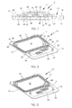
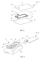
- the display unit aperture 22 of the body portion 20 is dimensioned to receive a display unit 21 of a mobile point-of-sales or POS terminal 23. See Figure 9 .
- the body portion 20 therefore extends around a perimeter of a screen 25 of the display unit 21 of the POS terminal 23, sitting recessed relative thereto and just below a front surface 27 of a terminal housing 29.
- antenna circuit 10 within the terminal housing 29 and forming a wireless radio-frequency communication circuit, such as a RFID circuit or a NFC circuit, can be considered and, for example, locating the antenna circuit 10 to encircle a data-entry user-interface 31, such as a keyboard 33, provided on the front surface 27 of the terminal housing 29 may be convenient, thereby enabling a larger antenna coil to be utilised.
- a data-entry user-interface 31 such as a keyboard 33
- the body portion 20 of the substrate 12 includes an inner end portion 30 of the antenna coil 14 and an outer end portion 32. Both the inner and outer end portions 30, 32 are adjacent to a proximal end 34 of the tail portion 24.
- the antenna coil 14 extends around the body portion 20, terminating at the inner and outer end portions 30, 32, and at a free distal end 36 of the tail portion 24 in preparation for attachment of a suitable IC chip 37 (see Figure 8 ).
- the front major surface 38 of the substrate 12 is pre-laminated with at least one electrically conductive coating 40, for example, being or including in this case copper.
- the antenna coil 14 is formed by etching or other suitable processing, whereby the laminated electrically conductive coating 40 is partially removed down to the plastics base surface 42 of the substrate 12 to leave the electrically conductive trace 44 around the body portion 20 and along the tail portion 24.
- the laminated electrically conductive coating 40 is wholly removed from the mounting portion 26.
- the crossover element 16 therefore needs to be applied to bridge a portion 46 of the antenna coil 14 which passes between the inner and outer end portions 30, 32 and to the tail portion 24.
- the crossover element 16 of this embodiment bridges only one coil, turn or trace of the antenna coil 14, the crossover element 16 may bridge multiple coils, turns or traces passing between the inner and outer end portions 30, 32, as necessity dictates.
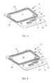
- an electrically insulative layer or dielectric layer 48 is first applied above and, in this case, on and overlapping the portion 46 of the trace extending between the inner and outer end portions 30, 32 of the antenna coil 14.
- the electrically insulative layer 48 has a first dimension which at least matches an outer lateral extent of the antenna coil 14, and a second dimension which at least substantially matches a separation between the inner and outer end portions 30, 32.
- the electrically insulative layer 48 may be a dielectric screen-printable UV-curable solvent-free ink, and for example may contain a urethane acrylate binder and/or magnesium silicate filler.
- an elongate first electrically conductive layer or trace 50 is applied above, and in this case on top of, the electrically insulative layer 48.
- a longitudinal extent of the first electrically conductive layer 50 overlaps the electrically insulative layer 48, thereby directly engaging the inner and outer end portions 30, 32 of the antenna coil 14.
- the first electrically conductive layer 50 is preferably a printable thin film ink comprising noble metal particles, such as silver.
- a noble metal is beneficial in preventing or reducing oxidation during manufacture, whilst also providing a suitable base layer for a subsequent electroplating process.
- the noble metal could be replaced or supplemented by non-noble metal electrically conductive particles, such as carbon.
- the first electrically conductive layer 50 is preferably a flowable and curable electrically conductive PTF ink, other dielectric materials and/or application processes may be considered.
- an elongate second electrically conductive layer or trace 52 is then applied above, and again in this case on top of, the first electrically conductive layer 50.
- the second electrically conductive layer 52 preferably does not contact the electrically insulative layer 48 but does engage with the first electrically conductive layer 50.
- a longitudinal extent of the second electrically conductive layer 52 is also greater than that of the first electrically conductive layer 50.
- the second electrically conductive layer 52 overlaps the first electrically conductive layer 50 in at least a longitudinal direction and directly engages the inner and outer end portions 30, 32 of the antenna coil 14 at first engagement regions 54 adjacent to second engagement regions 55 of the first electrically conductive layer 50.
- the second electrically conductive layer 52 is preferably an electroplated metal layer, in this case being copper.
- the first electrically conductive layer 50 provides a suitably platable base layer, thereby allowing the second electrically conductive layer 52 to be electroplated both thereon and onto the inner and outer end portions 30, 32 of the antenna coil 14 to complete the crossover element 16.
- the crossover element 16 can thus be more easily tuned to achieve a resistance which matches or substantially matches that of the antenna coil 14. This leads to improved antenna performance due to the lack of significant change to current flow direction and the maintenance of a common electrically conductive material, which is particularly beneficial for broadcast antennas but also useful for reading and receiving antennas.
- the retaining of a low antenna profile due to the absence of any over coating or layers on the rear major surface 18 of the substrate 12 is also beneficial in allowing incorporation of the wireless radio-frequency communication circuit to which the antenna circuit 10 forms a part into existing POS terminal designs.
- this new antenna circuit 10 can be applied to a broadcastable or non-broadcastable smart-card 70 and/or non-contact bank card 72. See Figures 8 and 9 .
- the smart-card 70 or non-contact bank card 72 comprises a card body 74 formed of top and bottom substrates 76, 78 and the circuit substrate 12 interposed there between.
- the tail portion 24 of the substrate 12 is dispensed with.
- a contact pad 80 is provided within the circuit antenna 14, and this includes an outwardly-facing electrical card-reader contact 82.
- the IC chip 37 is attached to an underside of the contact pad 80, so as to be in electrical communication therewith, using flip-chip mounting technology or any other suitable electrical connection means.
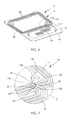
- the single-sided antenna circuit 10 comprises the circuit substrate 12, antenna coil 14 on the front major surface 38 of the substrate 12, and a crossover element 116 also on the front major surface 38 of the substrate 12.
- the crossover element 116 includes a rigid electrically insulative housing 156 for bridging the or each turn of the antenna coil 14 which passes between the inner and outer end portions 30, 32, and an electrical conductor 158 which passes through the electrically insulative housing 156 to electrically interconnect the inner and outer end portions 30, 32 of the antenna coil 14.
- the electrical conductor 158 may be formed on an electrically insulative core or former, and this may be a ceramic core or former.
- the electrical conductor 158 is formed of a same material as that of the coils, traces or turns of the antenna coil 14. Therefore, in this case, it is preferable that the electrical conductor 158 is copper.
- Terminal ends 160 of the electrical conductor 158 extend from the electrically insulative housing 156, and directly engage the inner and outer end portions 30, 32, respectively, for example, by soldering or brazing.
- a resistor 162 may have a zero ohm resistance.
- the resistor 162 may be of a higher profile than the crossover element 116 of the first embodiment, thereby making incorporation into an existing design of a device more complicated without a redesign.
- the crossover element 116 of the second embodiment may be a functional IC chip, a chip capacitor or other suitable electrical device.
- the electrically insulative housing 156 would be an IC chip housing or a capacitor housing, as required.
- such electrical device would be a dummy or passive component, being utilised solely for the purpose of the crossover and therefore not having any other function or forming a dynamic part of a circuit.
- the electrical conductor 158 of the second embodiment is of a different material than the antenna coil 14, then a circuit resistance will alter resulting in the potential of a performance drop.
- the arrangement of the second embodiment may be more suited to a non-broadcast wireless radio-communication circuit, such as that incorporated with a smart card or non-contact bank card.
- any suitable far-field or near-field wireless radio-frequency communication can utilise the above-described antenna circuit.
Abstract
Description
- The present invention relates to an antenna circuit, to a wireless radio-frequency communication circuit, for example being a RFID circuit and/or a near-field communication (NFC) circuit, having such an antenna circuit, to a mobile point-of sales terminal utilising the antenna circuit, and to a method of forming a low-profile crossover element on a single-sided antenna circuit.
- At present, to provide a low-profile antenna circuit, a flexible circuit substrate is laminated on both major opposing surfaces with a metallic electrically conductive layer, in this case being copper. An antenna coil for use with an RFID circuit, NFC circuit or other wireless radio-frequency communication circuit is then etched or otherwise provided on a front said major surface, and a crossover element is provided on a rear said major surface. The crossover element is a short link track or trace of copper left by the removal of the rest of the copper layer on the rear major surface.
- Through holes or vias are then formed between the front and rear major surfaces, interconnecting an inner end portion of the antenna coil with a first end of the crossover element and an outer end portion of the antenna coil with a second end of the crossover element. The through holes are then plated to electrically connect the antenna coil and the crossover element, thereby forming the antenna circuit.
- However, the removal of such a large amount of copper from the rear major surface causes significant waste and increases manufacturing cost. The through holes can only be formed using laser or highly accurate drilling technology, which again leads to increased manufacturing time and a potentially higher scrap rate due to drilling position inconsistencies. Furthermore, the plating of the through holes disrupts the current flow, thereby altering the resistance of the circuit and thus reducing operational performance.
- The present invention seeks to provide a solution to these problems.
- According to a first aspect of the invention, there is provided an antenna circuit comprising a substrate, an antenna coil on only one side of the substrate, and a low-profile crossover element on the one side of the substrate and which bridges at least one turn of the antenna coil to electrically interconnect an inner end portion and an outer end portion of the antenna coil, the crossover element including a, preferably overprintable, electrically insulative layer on or adjacent to the turn of the antenna coil, a, preferably printable, first electrically conductive layer above the electrically insulative layer, and a, preferably electrodeposited, second electrically conductive layer which is above the first electrically conductive layer and which is of a different electrically conductive material.
- Preferably, the electrically insulative layer on or adjacent to the turn of the antenna coil is overprintable, the first electrically conductive layer above the electrically insulative layer is printable, and the second electrically conductive layer which is above the first electrically conductive layer and which is of a different electrically conductive material is electrodeposited.
- Optionally, the first electrically conductive layer may include noble metal particles, and in this case it is preferable that silver particles are utilised. This reduces or eliminates oxidation, particularly during manufacture. As an alternative or in addition, carbon particles could be utilised. This may aid in reducing cost whilst still enabling good electrical conductivity and a base layer for forming the second electrically conductive layer thereon.
- Beneficially, the first electrically conductive layer may be a flowable conductive ink. This enables the crossover element to be quickly and easily applied across the antenna coil on the one side of the substrate.
- The second electrically conductive layer is preferably an electroplated layer. This provides a more conductively robust path for current travelling through the crossover element. Furthermore, the second electrically conductive layer may be a non-noble metal, and for example may conveniently be copper. This is beneficial in more accurately matching a resistance of the antenna coil with that of the crossover element.
- The inner end portion and the outer end portion of the antenna coil are preferably engaged with at least the first electrically conductive layer, which also overlaps the electrically insulative layer. This provides the crossover element with a robust connection to the antenna coil, which improves the longevity of the antenna circuit whilst also minimising the profile of the crossover element.
- Advantageously, the second electrically conductive layer may overlap the first electrically conductive layer to electrically engage the inner end portion and the outer end portion of the antenna coil. By utilising both first and second different electrically conductive layers, being applied by different application means, a more robust connection is achieved by the crossover element with the end portions of the antenna coil.
- According to a second aspect of the invention, there is provided a wireless radio-frequency communication circuit comprising an antenna circuit in accordance with the first aspect of the invention, and an IC chip electrically connected to the antenna coil, the substrate including a body portion and a chip-mounting portion cantilevered to the body portion, whereby the antenna coil extends around the body portion and along the chip-mounting portion, the IC chip being mounted on the chip-mounting portion so as to be in electrical communication with the antenna coil thereon.
- Preferably, the mounting portion is a cantilevered tail which extends away from the body portion and the portion of the antenna coil provided thereon. This is advantageous in that the central region of the body portion bounded by the antenna coil may this be apertured for receiving componentry, for example, a display unit there within or there through.
- The substrate may further comprise a housing-mounting portion which extends from the body portion and around the tail portion. This not only protects the chip-mounting portion, but also increases a number of fastening locations for attaching the wireless radio-frequency communication circuit to a device housing or support.
- According to a third aspect of the invention, there is provided a mobile point-of-sales terminal comprising a handholdable housing, a data-entry user-interface at a surface of the handholdable housing, a display unit having a display screen on the handholdable housing for displaying data inputted via the data-entry user-interface, and a wireless radio-frequency communication circuit in accordance with the second aspect of the invention in the handholdable housing and through which the display unit extends.
- According to a fourth aspect of the invention, there is provided a method of forming a low-profile crossover element on a single-sided antenna circuit, comprising the steps of: a] printing at a first side of a substrate of the antenna circuit a first electrically conductive layer on an electrically insulative layer bridging at least one turn of an antenna coil also on the said first side of the substrate; and b] electroplating a second electrically conductive layer on the first electrically conductive layer to electrically interconnect inner and outer end portions of the antenna coil.
- According to a fifth aspect of the invention, there is provided an antenna circuit comprising a substrate, an antenna coil on only one side of the substrate, and a crossover element on the said one side of the substrate and which bridges at least one turn of the antenna coil to electrically interconnect an inner end portion and an outer end portion of the antenna coil, the crossover element comprising a rigid electrically insulative housing for bridging the at least one turn of the antenna coil, and an electrical conductor which extends through the electrically insulative housing and which electrically interconnects the inner and outer end portions of the antenna coil.
- A preferred embodiment of the invention will now be described, by way of example only, with reference to figures of the accompanying drawings. In the figures, identical structures, elements or parts that appear in more than one figure are generally labelled with a same reference numeral in all the figures in which they appear. Dimensions of components and features shown in the figures are generally chosen for convenience and clarity of presentation and are not necessarily shown to scale. The figures are listed below.
-
Figure 1 is a diagrammatic cross-sectional view of a first embodiment of an antenna circuit having a crossover element applied between end portions of an antenna coil, in accordance with the first to fourth aspects of the invention; -
Figure 2 is a perspective view of an imageable circuit substrate having an antenna coil on a front major surface thereof; -
Figure 3 is a view similar to that ofFigure 2 , showing the antenna coil with a dielectric patch applied; -
Figure 4 shows a first electrically conductive trace applied to the dielectric patch; -
Figure 5 shows a second electrically conductive trace applied to the first electrically conductive trace ofFigure 4 ; -
Figure 6 is a perspective view of a second embodiment of an antenna circuit having a different crossover element applied between end portions of an antenna coil, in accordance with the fifth aspect of the invention; -
Figure 7 is an enlarged portion of the antenna circuit shown inFigure 6 , more clearly showing the crossover element; -
Figure 8 shows an exploded perspective view of a broadcastable or non-broadcastable smart-card or non-contact bank card, having the antenna circuit with crossover element; and -
Figure 9 shows a point-of-sales terminal having the antenna circuit with crossover element therein, and being used in conjunction with the smart-card or bank card shown inFigure 8 . - Referring firstly to
Figures 1 and5 of the drawings, a first embodiment of anantenna circuit 10 comprises a, preferably flexible and imageable,circuit substrate 12, anantenna coil 14, and a low-profile crossover element 16. The flexibleimageable circuit substrate 12 is unlaminated on a rearmajor surface 18, thereby being devoid of an electrically conductive layer, trace or circuit in particular relating to theantenna coil 14. More particularly, the rearmajor surface 18 of thesubstrate 12 presents a plastics non-metallised surface, and conveniently is supplied as such without requiring processing to remove a conductive laminate layer therefrom. - The
substrate 12, in this embodiment, is stamped or otherwise formed to provide a continuousunbroken body portion 20 defining adisplay unit aperture 22, atail portion 24 which extends in a cantilevered manner from one side of thebody portion 20 and away from thedisplay unit aperture 22, and an elongate strip-like mounting portion 26 which extends from opposing corners on a longitudinal side of thebody portion 20 to encompass and thereby protect thetail portion 24. - Although the
display unit aperture 22 is provided, the substrate may be unapertured or have apertures of different sizes as necessity dictates. Additionally or alternatively, although thetail portion 24 preferably extends away from theaperture 22, it may extend into the or an aperture of the substrate, or may be dispensed with if theantenna coil 14 is entirely provided on the body portion. -
Mounting apertures 28 are provided on thesubstrate 12 for connection to a housing, chassis or module of a device in which theantenna circuit 10 is to be incorporated. In this case, two saidmounting apertures 28 are provided at diametrically opposing interior corners of thebody portion 20 and two saidmounting apertures 28 are provided at diametrically opposing interior corners of themounting portion 26. - In this case, the
display unit aperture 22 of thebody portion 20 is dimensioned to receive adisplay unit 21 of a mobile point-of-sales orPOS terminal 23. SeeFigure 9 . Thebody portion 20 therefore extends around a perimeter of ascreen 25 of thedisplay unit 21 of thePOS terminal 23, sitting recessed relative thereto and just below afront surface 27 of aterminal housing 29. However, other positions of theantenna circuit 10 within theterminal housing 29 and forming a wireless radio-frequency communication circuit, such as a RFID circuit or a NFC circuit, can be considered and, for example, locating theantenna circuit 10 to encircle a data-entry user-interface 31, such as akeyboard 33, provided on thefront surface 27 of theterminal housing 29 may be convenient, thereby enabling a larger antenna coil to be utilised. - The
body portion 20 of thesubstrate 12 includes aninner end portion 30 of theantenna coil 14 and anouter end portion 32. Both the inner andouter end portions proximal end 34 of thetail portion 24. Theantenna coil 14 extends around thebody portion 20, terminating at the inner andouter end portions distal end 36 of thetail portion 24 in preparation for attachment of a suitable IC chip 37 (seeFigure 8 ). - The front
major surface 38 of thesubstrate 12 is pre-laminated with at least one electricallyconductive coating 40, for example, being or including in this case copper. Theantenna coil 14 is formed by etching or other suitable processing, whereby the laminated electricallyconductive coating 40 is partially removed down to theplastics base surface 42 of thesubstrate 12 to leave the electricallyconductive trace 44 around thebody portion 20 and along thetail portion 24. The laminated electricallyconductive coating 40 is wholly removed from the mountingportion 26. - The
crossover element 16 therefore needs to be applied to bridge aportion 46 of theantenna coil 14 which passes between the inner andouter end portions tail portion 24. Although thecrossover element 16 of this embodiment bridges only one coil, turn or trace of theantenna coil 14, thecrossover element 16 may bridge multiple coils, turns or traces passing between the inner andouter end portions - To apply the
crossover element 16, reference is now also made toFigures 2 to 4 of the drawings, in addition toFigures 1 and5 . As shown inFigures 2 and5 , an electrically insulative layer ordielectric layer 48 is first applied above and, in this case, on and overlapping theportion 46 of the trace extending between the inner andouter end portions antenna coil 14. Preferably, theelectrically insulative layer 48 has a first dimension which at least matches an outer lateral extent of theantenna coil 14, and a second dimension which at least substantially matches a separation between the inner andouter end portions - Conveniently, the
electrically insulative layer 48 may be a dielectric screen-printable UV-curable solvent-free ink, and for example may contain a urethane acrylate binder and/or magnesium silicate filler. - Referring to
Figure 3 andFigure 5 , an elongate first electrically conductive layer ortrace 50 is applied above, and in this case on top of, theelectrically insulative layer 48. A longitudinal extent of the first electricallyconductive layer 50 overlaps theelectrically insulative layer 48, thereby directly engaging the inner andouter end portions antenna coil 14. - The first electrically
conductive layer 50 is preferably a printable thin film ink comprising noble metal particles, such as silver. The use of a noble metal is beneficial in preventing or reducing oxidation during manufacture, whilst also providing a suitable base layer for a subsequent electroplating process. However, it is feasible that the noble metal could be replaced or supplemented by non-noble metal electrically conductive particles, such as carbon. - Although the first electrically
conductive layer 50 is preferably a flowable and curable electrically conductive PTF ink, other dielectric materials and/or application processes may be considered. - Referring to
Figures 4 and 5 , an elongate second electrically conductive layer ortrace 52 is then applied above, and again in this case on top of, the first electricallyconductive layer 50. The second electricallyconductive layer 52 preferably does not contact theelectrically insulative layer 48 but does engage with the first electricallyconductive layer 50. A longitudinal extent of the second electricallyconductive layer 52 is also greater than that of the first electricallyconductive layer 50. As such, the second electricallyconductive layer 52 overlaps the first electricallyconductive layer 50 in at least a longitudinal direction and directly engages the inner andouter end portions antenna coil 14 atfirst engagement regions 54 adjacent tosecond engagement regions 55 of the first electricallyconductive layer 50. - The second electrically
conductive layer 52 is preferably an electroplated metal layer, in this case being copper. The first electricallyconductive layer 50 provides a suitably platable base layer, thereby allowing the second electricallyconductive layer 52 to be electroplated both thereon and onto the inner andouter end portions antenna coil 14 to complete thecrossover element 16. - By providing an overprintable electrically insulative
layer 48, a printable first electricallyconductive layer 50 and an electrodeposited second electricallyconductive layer 52, thecrossover element 16 can thus be more easily tuned to achieve a resistance which matches or substantially matches that of theantenna coil 14. This leads to improved antenna performance due to the lack of significant change to current flow direction and the maintenance of a common electrically conductive material, which is particularly beneficial for broadcast antennas but also useful for reading and receiving antennas. The retaining of a low antenna profile due to the absence of any over coating or layers on the rearmajor surface 18 of thesubstrate 12 is also beneficial in allowing incorporation of the wireless radio-frequency communication circuit to which theantenna circuit 10 forms a part into existing POS terminal designs. - Additionally, or alternatively, this
new antenna circuit 10 can be applied to a broadcastable or non-broadcastable smart-card 70 and/or non-contact bank card 72. SeeFigures 8 and 9 . - Referring to
Figure 8 , the smart-card 70 or non-contact bank card 72 comprises acard body 74 formed of top andbottom substrates circuit substrate 12 interposed there between. In this case, thetail portion 24 of thesubstrate 12 is dispensed with. - A
contact pad 80 is provided within thecircuit antenna 14, and this includes an outwardly-facing electrical card-reader contact 82. - The
IC chip 37 is attached to an underside of thecontact pad 80, so as to be in electrical communication therewith, using flip-chip mounting technology or any other suitable electrical connection means. - Referring now to
Figures 6 and 7 of the drawings, a second embodiment of anantenna circuit 10 will now be described. The same references as used in the first embodiment are used to denote identical or similar parts, and therefore further detailed description is omitted. - The single-
sided antenna circuit 10 comprises thecircuit substrate 12,antenna coil 14 on the frontmajor surface 38 of thesubstrate 12, and acrossover element 116 also on the frontmajor surface 38 of thesubstrate 12. However, in this case, thecrossover element 116 includes a rigid electricallyinsulative housing 156 for bridging the or each turn of theantenna coil 14 which passes between the inner andouter end portions electrical conductor 158 which passes through the electricallyinsulative housing 156 to electrically interconnect the inner andouter end portions antenna coil 14. - The
electrical conductor 158 may be formed on an electrically insulative core or former, and this may be a ceramic core or former. - Preferably, the
electrical conductor 158 is formed of a same material as that of the coils, traces or turns of theantenna coil 14. Therefore, in this case, it is preferable that theelectrical conductor 158 is copper. - Terminal ends 160 of the
electrical conductor 158 extend from the electricallyinsulative housing 156, and directly engage the inner andouter end portions - It may be convenient, in this second embodiment, to utilise a
resistor 162 as thecrossover element 116, and for example, theresistor 162 may have a zero ohm resistance. However, such aresistor 162 may be of a higher profile than thecrossover element 116 of the first embodiment, thereby making incorporation into an existing design of a device more complicated without a redesign. - Alternatively, the
crossover element 116 of the second embodiment may be a functional IC chip, a chip capacitor or other suitable electrical device. In these cases, the electricallyinsulative housing 156 would be an IC chip housing or a capacitor housing, as required. Preferably, such electrical device would be a dummy or passive component, being utilised solely for the purpose of the crossover and therefore not having any other function or forming a dynamic part of a circuit. - Furthermore, if the
electrical conductor 158 of the second embodiment is of a different material than theantenna coil 14, then a circuit resistance will alter resulting in the potential of a performance drop. - Consequently, the arrangement of the second embodiment may be more suited to a non-broadcast wireless radio-communication circuit, such as that incorporated with a smart card or non-contact bank card.
- Although RFID and NFC have been suggested as applications, any suitable far-field or near-field wireless radio-frequency communication can utilise the above-described antenna circuit.
- It is thus possible to provide a single-sided antenna circuit which maintains a low-profile whilst not only improving antenna performance but also significantly reducing wasted material by not requiring an electrically conductive laminate on both sides of a circuit substrate.
- In the description and claims of the present application, each of the verbs "comprise", "include", "contain" and "have", and variations thereof, are used in an inclusive sense, to specify the presence of the stated item or feature but do not preclude the presence of additional items or features.
- It is appreciated that certain features of the invention, which are, for clarity, described in the context of separate embodiments, may also be provided in combination in a single embodiment. Conversely, various features of the invention which are, for brevity, described in the context of a single embodiment, may also be provided separately or in any suitable sub-combination.
- The embodiments described above are provided by way of examples only, and various other modifications will be apparent to persons skilled in the field without departing from the scope of the invention as defined by the appended claims.
Claims (15)
- An antenna circuit comprising a substrate (12), an antenna coil (14) on only one side of the substrate, and a low-profile crossover element (16, 116) on said one side of the substrate and which bridges at least one turn of the antenna coil to electrically interconnect an inner end portion (30) and an outer end portion (32) of the antenna coil, the crossover element comprising an electrically insulative layer (48) on or adjacent to said turn of the antenna coil, a first electrically conductive layer (50) above the electrically insulative layer, and a second electrically conductive layer (52) which is above the first electrically conductive layer and which is of a different electrically conductive material.
- An antenna circuit as claimed in Claim 1, wherein the first electrically conductive layer (50) is a printable thin film material or a flowable conductive ink.
- An antenna circuit as claimed in Claim 1 or 2, wherein the first electrically conductive layer (50) includes silver and/or carbon particles.
- An antenna circuit as claimed in any one of the preceding claims, wherein the first electrically conductive layer (50) is non-oxidative or is resistant to oxidation.
- An antenna circuit as claimed in any one of the preceding claims, wherein the second electrically conductive layer (52) is an electroplated layer.
- An antenna circuit as claimed in any one of the preceding claims, wherein the second electrically conductive layer (52) is copper.
- An antenna circuit as claimed in any one of the preceding claims, wherein the first electrically conductive layer (50) overlaps the electrically insulative layer (48) to physically and electrically engage the inner end portion (30) and the outer end portion (32) of the antenna coil (14).
- An antenna circuit as claimed in any one of the preceding claims, wherein the second electrically conductive layer (52) overlaps the first electrically conductive layer (50) to physically and electrically engage the inner end portion (30) and the outer end portion (32) of the antenna coil (14).
- A wireless radio-frequency communication circuit comprising an antenna circuit (10) as claimed in any one of the preceding claims, and an IC chip (37) electrically connected to the antenna coil (14), the substrate including a body portion (20) and a chip-mounting portion (24) cantilevered to the body portion, whereby the antenna coil (14) extends around the body portion (20) and along the chip-mounting portion (24), the IC chip (37) being mounted on the chip-mounting portion so as to be in electrical communication with the antenna coil thereon.
- A wireless radio-frequency communication circuit as claimed in Claim 9, wherein the chip-mounting portion (24) extends away from the body portion (20) and the portion of the antenna coil (14) provided thereon.
- A wireless radio-frequency communication circuit as claimed in Claim 9 or 10, wherein the body portion (20) includes a central aperture (22) for receiving a display unit (21) and which is surrounded by the antenna coil (14).
- A wireless radio-frequency communication circuit as claimed in Claim 9, 10 or 11, wherein the substrate (12) further comprises a housing-mounting portion (26) which extends from the body portion (20) and around the chip-mounting portion (24).
- A mobile point-of-sales terminal comprising a handholdable housing (29), a data-entry user-interface at a surface of the handholdable housing, a display unit (21) having a display screen (25) on the handholdable housing for displaying data inputted via the data-entry user-interface, and a wireless radio-frequency communication circuit as claimed in Claim 9, 10, 11 or 12 in the handholdable housing (29) and through which the display unit extends.
- A method of forming a low-profile crossover element (16, 116) on a single-sided antenna circuit (10), comprising the steps of: a] printing at a first side of a substrate (12) of the antenna circuit a first electrically conductive layer (50) on an electrically insulative layer (48) bridging at least one turn of an antenna coil (14) also on said first side of the substrate; and b] electroplating a second electrically conductive layer (52) on the first electrically conductive layer (50) to electrically interconnect inner and outer end portions (30, 32) of the antenna coil.
- An antenna circuit comprising a substrate (12), an antenna coil (14) on only one side of the substrate, and a crossover element (116) on said one side of the substrate and which bridges at least one turn of the antenna coil to electrically interconnect an inner end portion (30) and an outer end portion (32) of the antenna coil, the crossover element (116) comprising a rigid electrically insulative housing (156) for bridging said at least one turn of the antenna coil, and an electrical conductor (158) which extends through the electrically insulative housing and which electrically interconnects the inner and outer end portions (30, 32) of the antenna coil.
Applications Claiming Priority (1)
| Application Number | Priority Date | Filing Date | Title |
|---|---|---|---|
| CN201310357214.XA CN104377439B (en) | 2013-08-15 | 2013-08-15 | Antenna circuit and manufacturing method |
Publications (1)
| Publication Number | Publication Date |
|---|---|
| EP2838046A1 true EP2838046A1 (en) | 2015-02-18 |
Family
ID=51292871
Family Applications (1)
| Application Number | Title | Priority Date | Filing Date |
|---|---|---|---|
| EP14180359.3A Withdrawn EP2838046A1 (en) | 2013-08-15 | 2014-08-08 | Antenna circuit |
Country Status (6)
| Country | Link |
|---|---|
| US (1) | US9152833B2 (en) |
| EP (1) | EP2838046A1 (en) |
| JP (1) | JP6450110B2 (en) |
| KR (1) | KR102156821B1 (en) |
| CN (1) | CN104377439B (en) |
| BR (1) | BR102014020210A2 (en) |
Families Citing this family (8)
| Publication number | Priority date | Publication date | Assignee | Title |
|---|---|---|---|---|
| KR102280037B1 (en) * | 2015-07-29 | 2021-07-21 | 삼성전자주식회사 | A power supply device for a built-in antenna provided in the display |
| US10937019B2 (en) | 2016-06-08 | 2021-03-02 | Square, Inc. | Wireless communication system with auxiliary antenna |
| US10318953B2 (en) * | 2016-06-29 | 2019-06-11 | Square, Inc. | Near field communication flex circuit |
| US10594599B2 (en) | 2016-08-26 | 2020-03-17 | Cisco Technology, Inc. | Fibre channel fabric slow drain mitigation |
| US10949189B2 (en) | 2017-06-28 | 2021-03-16 | Square, Inc. | Securely updating software on connected electronic devices |
| US10635820B1 (en) | 2017-09-29 | 2020-04-28 | Square, Inc. | Update policy-based anti-rollback techniques |
| US20200409416A1 (en) * | 2019-06-27 | 2020-12-31 | Ncr Corporation | Flexible point of sale device |
| US11437851B2 (en) * | 2020-02-11 | 2022-09-06 | Dupont Electronics, Inc. | Plated copper conductor structures for wireless charging system and manufacture thereof |
Citations (9)
| Publication number | Priority date | Publication date | Assignee | Title |
|---|---|---|---|---|
| US20040189625A1 (en) * | 2003-03-14 | 2004-09-30 | Seiko Epson Corporation | Display device and electronic apparatus |
| EP1600887A2 (en) * | 2004-05-25 | 2005-11-30 | Nec Corporation | Mobile communication terminal |
| JP2006165050A (en) * | 2004-12-02 | 2006-06-22 | Murata Mfg Co Ltd | Transformer integrated circuit board |
| WO2006073525A1 (en) * | 2005-01-07 | 2006-07-13 | Honeywell International Inc. | Hand held rfid reader with dipole antenna |
| WO2007019762A1 (en) * | 2005-08-19 | 2007-02-22 | Byd Company Limited | Housing for mobile phone and mobile phone having the same |
| US20070090955A1 (en) * | 2005-10-25 | 2007-04-26 | Checkpoint Systems, Inc. | Capacitor strap |
| CN101609924A (en) * | 2008-06-20 | 2009-12-23 | 上海中京电子标签集成技术有限公司 | A kind of high-frequency tag antenna that can realize that many moneys chip uses |
| EP2482261A2 (en) * | 2011-01-31 | 2012-08-01 | Metrologic Instruments, Inc. | Bar code symbol reading system employing EAS-enabling faceplate bezel |
| WO2013141658A1 (en) * | 2012-03-23 | 2013-09-26 | 엘지이노텍 주식회사 | Antenna assembly and method for manufacturing same |
Family Cites Families (21)
| Publication number | Priority date | Publication date | Assignee | Title |
|---|---|---|---|---|
| JPS5989576U (en) * | 1982-12-06 | 1984-06-18 | 株式会社東芝 | Wiring chip |
| JPH0465024A (en) * | 1990-07-03 | 1992-03-02 | Rohm Co Ltd | Jumper chip |
| JP2770693B2 (en) * | 1992-12-21 | 1998-07-02 | 日本ケミコン株式会社 | Thick film multilayer circuit board |
| US5541399A (en) | 1994-09-30 | 1996-07-30 | Palomar Technologies Corporation | RF transponder with resonant crossover antenna coil |
| JP2003508833A (en) | 1999-08-31 | 2003-03-04 | コーニンクレッカ フィリップス エレクトロニクス エヌ ヴィ | Data storage medium having integrated circuit and transmission coil |
| JP2001217639A (en) * | 2000-01-31 | 2001-08-10 | Toppan Forms Co Ltd | Antenna for contactless type data transmission and reception body |
| US20020020491A1 (en) * | 2000-04-04 | 2002-02-21 | Price David M. | High speed flip chip assembly process |
| JP2002197435A (en) * | 2000-12-27 | 2002-07-12 | Toppan Forms Co Ltd | Method for forming antenna circuit for non-contacting ic medium using electron beam and the medium provided with the circuit |
| US6717502B2 (en) * | 2001-11-05 | 2004-04-06 | Atheros Communications, Inc. | Integrated balun and transformer structures |
| US6665193B1 (en) | 2002-07-09 | 2003-12-16 | Amerasia International Technology, Inc. | Electronic circuit construction, as for a wireless RF tag |
| US7274297B2 (en) * | 2004-07-01 | 2007-09-25 | Intermec Ip Corp. | RFID tag and method of manufacture |
| US7286053B1 (en) * | 2004-07-31 | 2007-10-23 | Kovio, Inc. | Electronic article surveillance (EAS) tag/device with coplanar and/or multiple coil circuits, an EAS tag/device with two or more memory bits, and methods for tuning the resonant frequency of an RLC EAS tag/device |
| CN2833904Y (en) | 2005-07-29 | 2006-11-01 | 北京握奇数据系统有限公司 | Antenna for plug-type double-interface smart card |
| US7555826B2 (en) | 2005-12-22 | 2009-07-07 | Avery Dennison Corporation | Method of manufacturing RFID devices |
| MX2009007721A (en) * | 2007-01-18 | 2009-07-30 | Checkpoint Systems Inc | Permanently destructible resonant circuit with non-self-healing capacitor. |
| DE102007028357A1 (en) * | 2007-06-15 | 2008-12-24 | Ksw Microtec Ag | transponder card |
| JPWO2009104778A1 (en) | 2008-02-20 | 2011-06-23 | リンテック株式会社 | Antenna circuit |
| KR101179306B1 (en) * | 2010-05-11 | 2012-09-03 | 삼성전기주식회사 | Case of electronic device having antenna pattern embeded therein, mould and method for manufacturing the same |
| JP5321989B2 (en) * | 2010-05-11 | 2013-10-23 | サムソン エレクトロ−メカニックス カンパニーリミテッド. | Electronic device case in which antenna pattern is embedded, manufacturing mold and manufacturing method thereof |
| CN102891359A (en) * | 2011-07-22 | 2013-01-23 | 深圳市长盈精密技术股份有限公司 | Manufacturing process of mobile phone built-in printed antenna |
| WO2013016283A1 (en) * | 2011-07-22 | 2013-01-31 | Virginia Tech Intellectual Properties, Inc. | Volatile/non-volatile floating electrode logic/memory cell |
-
2013
- 2013-08-15 CN CN201310357214.XA patent/CN104377439B/en not_active Expired - Fee Related
-
2014
- 2014-08-08 EP EP14180359.3A patent/EP2838046A1/en not_active Withdrawn
- 2014-08-14 BR BR102014020210A patent/BR102014020210A2/en not_active Application Discontinuation
- 2014-08-14 KR KR1020140105912A patent/KR102156821B1/en active IP Right Grant
- 2014-08-15 JP JP2014165358A patent/JP6450110B2/en not_active Expired - Fee Related
- 2014-08-15 US US14/460,753 patent/US9152833B2/en not_active Expired - Fee Related
Patent Citations (9)
| Publication number | Priority date | Publication date | Assignee | Title |
|---|---|---|---|---|
| US20040189625A1 (en) * | 2003-03-14 | 2004-09-30 | Seiko Epson Corporation | Display device and electronic apparatus |
| EP1600887A2 (en) * | 2004-05-25 | 2005-11-30 | Nec Corporation | Mobile communication terminal |
| JP2006165050A (en) * | 2004-12-02 | 2006-06-22 | Murata Mfg Co Ltd | Transformer integrated circuit board |
| WO2006073525A1 (en) * | 2005-01-07 | 2006-07-13 | Honeywell International Inc. | Hand held rfid reader with dipole antenna |
| WO2007019762A1 (en) * | 2005-08-19 | 2007-02-22 | Byd Company Limited | Housing for mobile phone and mobile phone having the same |
| US20070090955A1 (en) * | 2005-10-25 | 2007-04-26 | Checkpoint Systems, Inc. | Capacitor strap |
| CN101609924A (en) * | 2008-06-20 | 2009-12-23 | 上海中京电子标签集成技术有限公司 | A kind of high-frequency tag antenna that can realize that many moneys chip uses |
| EP2482261A2 (en) * | 2011-01-31 | 2012-08-01 | Metrologic Instruments, Inc. | Bar code symbol reading system employing EAS-enabling faceplate bezel |
| WO2013141658A1 (en) * | 2012-03-23 | 2013-09-26 | 엘지이노텍 주식회사 | Antenna assembly and method for manufacturing same |
Non-Patent Citations (1)
| Title |
|---|
| LOCHUN D ET AL: "Reel-to-reel manufacturability of flexible electrical interconnects and radio-frequency identification structures", 2002 PROCEEDINGS 52ND. ELECTRONIC COMPONENTS AND TECHNOLOGY CONFERENCE. ECTC 2002. SAN DIEGO, CA, MAY 28 - 31, 2002; [PROCEEDINGS OF THE ELECTRONIC COMPONENTS AND TECHNOLOGY CONFERENCE], NEW YORK, NY : IEEE, US, vol. CONF. 52, 28 May 2002 (2002-05-28), pages 686 - 689, XP010747704, ISBN: 978-0-7803-7430-0, DOI: 10.1109/ECTC.2002.1008172 * |
Also Published As
| Publication number | Publication date |
|---|---|
| JP6450110B2 (en) | 2019-01-09 |
| CN104377439B (en) | 2019-08-27 |
| JP2015037327A (en) | 2015-02-23 |
| KR102156821B1 (en) | 2020-09-17 |
| US9152833B2 (en) | 2015-10-06 |
| CN104377439A (en) | 2015-02-25 |
| KR20150020138A (en) | 2015-02-25 |
| US20150048163A1 (en) | 2015-02-19 |
| BR102014020210A2 (en) | 2015-12-01 |
Similar Documents
| Publication | Publication Date | Title |
|---|---|---|
| US9152833B2 (en) | Antenna circuit | |
| US8284117B2 (en) | Antenna device and method of manufacturing the same | |
| US6665193B1 (en) | Electronic circuit construction, as for a wireless RF tag | |
| CN104092019B (en) | Wireless IC device and component for wireless IC device | |
| JP2009111986A (en) | Radio frequency identification tag device | |
| US9390365B2 (en) | Integrated circuit module for a dual-interface smart card | |
| US9991599B2 (en) | Antenna device, electronic apparatus, and method of mounting antenna device | |
| US10820418B2 (en) | Electronic module, method for manufacturing same and electronic device comprising a module of said type | |
| US10387764B2 (en) | RFID tag, article including the same, and RFID tag manufacturing method | |
| CN107491804B (en) | Chip card module and method for producing a chip card module | |
| CN103262101A (en) | Systems and methods for integrating radio-frequency identification circuitry into flexible circuits | |
| CN215871985U (en) | Circuit board, antenna package and display device | |
| US9033252B2 (en) | Communication module, connector, and connector-equipped communication module | |
| KR101469764B1 (en) | Antenna and method for manufacturing thereof | |
| US11948038B2 (en) | RFIC module and RFID tag | |
| JPWO2019098123A1 (en) | IC tag | |
| US20050174745A1 (en) | Electronic assembly | |
| CN218996050U (en) | Multifunctional RFID tag | |
| WO2008115022A1 (en) | Antenna for radio frequency identification and method of manufacturing the same | |
| US20120193804A1 (en) | Ohmic connection using widened connection zones in a portable electronic object | |
| US10587301B2 (en) | Wireless communications module | |
| KR101208085B1 (en) | Display on card having display unit and manufacturing method thereof | |
| JP2014220601A (en) | Antenna device | |
| JP2014236436A (en) | Antenna sheet and manufacturing method thereof | |
| CN105633044A (en) | Connecting member |
Legal Events
| Date | Code | Title | Description |
|---|---|---|---|
| 17P | Request for examination filed |
Effective date: 20140808 |
|
| AK | Designated contracting states |
Kind code of ref document: A1 Designated state(s): AL AT BE BG CH CY CZ DE DK EE ES FI FR GB GR HR HU IE IS IT LI LT LU LV MC MK MT NL NO PL PT RO RS SE SI SK SM TR |
|
| AX | Request for extension of the european patent |
Extension state: BA ME |
|
| PUAI | Public reference made under article 153(3) epc to a published international application that has entered the european phase |
Free format text: ORIGINAL CODE: 0009012 |
|
| RAP1 | Party data changed (applicant data changed or rights of an application transferred) |
Owner name: JOHNSON ELECTRIC S.A. |
|
| R17P | Request for examination filed (corrected) |
Effective date: 20150813 |
|
| RBV | Designated contracting states (corrected) |
Designated state(s): AL AT BE BG CH CY CZ DE DK EE ES FI FR GB GR HR HU IE IS IT LI LT LU LV MC MK MT NL NO PL PT RO RS SE SI SK SM TR |
|
| STAA | Information on the status of an ep patent application or granted ep patent |
Free format text: STATUS: EXAMINATION IS IN PROGRESS |
|
| 17Q | First examination report despatched |
Effective date: 20180409 |
|
| RAP1 | Party data changed (applicant data changed or rights of an application transferred) |
Owner name: JOHNSON ELECTRIC INTERNATIONAL AG |
|
| RIC1 | Information provided on ipc code assigned before grant |
Ipc: G06K 7/10 20060101ALI20201015BHEP Ipc: H01Q 7/00 20060101ALI20201015BHEP Ipc: G06K 19/077 20060101ALN20201015BHEP Ipc: H01Q 1/22 20060101AFI20201015BHEP |
|
| GRAP | Despatch of communication of intention to grant a patent |
Free format text: ORIGINAL CODE: EPIDOSNIGR1 |
|
| STAA | Information on the status of an ep patent application or granted ep patent |
Free format text: STATUS: GRANT OF PATENT IS INTENDED |
|
| RIC1 | Information provided on ipc code assigned before grant |
Ipc: H01Q 7/00 20060101ALI20201019BHEP Ipc: G06K 19/077 20060101ALN20201019BHEP Ipc: G06K 7/10 20060101ALI20201019BHEP Ipc: H01Q 1/22 20060101AFI20201019BHEP |
|
| RIC1 | Information provided on ipc code assigned before grant |
Ipc: H01Q 1/22 20060101AFI20201110BHEP Ipc: G06K 7/10 20060101ALI20201110BHEP Ipc: G06K 19/077 20060101ALN20201110BHEP Ipc: H01Q 7/00 20060101ALI20201110BHEP |
|
| INTG | Intention to grant announced |
Effective date: 20201124 |
|
| STAA | Information on the status of an ep patent application or granted ep patent |
Free format text: STATUS: THE APPLICATION IS DEEMED TO BE WITHDRAWN |
|
| 18D | Application deemed to be withdrawn |
Effective date: 20210407 |