EP2884585A1 - Broadband patch antenna and associated methods - Google Patents
Broadband patch antenna and associated methods Download PDFInfo
- Publication number
- EP2884585A1 EP2884585A1 EP14004195.5A EP14004195A EP2884585A1 EP 2884585 A1 EP2884585 A1 EP 2884585A1 EP 14004195 A EP14004195 A EP 14004195A EP 2884585 A1 EP2884585 A1 EP 2884585A1
- Authority
- EP
- European Patent Office
- Prior art keywords
- electrically conductive
- patch
- wings
- patch antenna
- antenna
- Prior art date
- Legal status (The legal status is an assumption and is not a legal conclusion. Google has not performed a legal analysis and makes no representation as to the accuracy of the status listed.)
- Granted
Links
- 238000000034 method Methods 0.000 title claims abstract description 27
- 239000000758 substrate Substances 0.000 claims abstract description 21
- 239000004020 conductor Substances 0.000 claims abstract description 12
- 230000008878 coupling Effects 0.000 claims description 4
- 238000010168 coupling process Methods 0.000 claims description 4
- 238000005859 coupling reaction Methods 0.000 claims description 4
- 230000010287 polarization Effects 0.000 description 16
- 230000005855 radiation Effects 0.000 description 11
- 238000004891 communication Methods 0.000 description 6
- 238000004519 manufacturing process Methods 0.000 description 6
- 239000002184 metal Substances 0.000 description 6
- 229910052751 metal Inorganic materials 0.000 description 6
- 230000004044 response Effects 0.000 description 6
- 240000003380 Passiflora rubra Species 0.000 description 3
- 238000005452 bending Methods 0.000 description 3
- 238000013461 design Methods 0.000 description 3
- 238000010586 diagram Methods 0.000 description 3
- 238000009966 trimming Methods 0.000 description 3
- 238000002679 ablation Methods 0.000 description 2
- 238000013459 approach Methods 0.000 description 2
- 230000008901 benefit Effects 0.000 description 2
- 230000015572 biosynthetic process Effects 0.000 description 2
- 238000009826 distribution Methods 0.000 description 2
- 239000000463 material Substances 0.000 description 2
- 238000012986 modification Methods 0.000 description 2
- 230000004048 modification Effects 0.000 description 2
- 238000005549 size reduction Methods 0.000 description 2
- 238000003786 synthesis reaction Methods 0.000 description 2
- RYGMFSIKBFXOCR-UHFFFAOYSA-N Copper Chemical compound [Cu] RYGMFSIKBFXOCR-UHFFFAOYSA-N 0.000 description 1
- 235000014676 Phragmites communis Nutrition 0.000 description 1
- 241000220317 Rosa Species 0.000 description 1
- 239000004809 Teflon Substances 0.000 description 1
- 229920006362 Teflon® Polymers 0.000 description 1
- 238000003491 array Methods 0.000 description 1
- 210000000007 bat wing Anatomy 0.000 description 1
- 230000005540 biological transmission Effects 0.000 description 1
- 230000008859 change Effects 0.000 description 1
- 230000000052 comparative effect Effects 0.000 description 1
- 150000001875 compounds Chemical class 0.000 description 1
- 229910052802 copper Inorganic materials 0.000 description 1
- 239000010949 copper Substances 0.000 description 1
- 230000005574 cross-species transmission Effects 0.000 description 1
- 230000003247 decreasing effect Effects 0.000 description 1
- 239000003989 dielectric material Substances 0.000 description 1
- 230000009977 dual effect Effects 0.000 description 1
- 230000000694 effects Effects 0.000 description 1
- 238000005530 etching Methods 0.000 description 1
- 230000003203 everyday effect Effects 0.000 description 1
- 230000005284 excitation Effects 0.000 description 1
- 238000010304 firing Methods 0.000 description 1
- 238000005286 illumination Methods 0.000 description 1
- 230000001939 inductive effect Effects 0.000 description 1
- 238000003801 milling Methods 0.000 description 1
- 238000010295 mobile communication Methods 0.000 description 1
- 238000005457 optimization Methods 0.000 description 1
- 235000012771 pancakes Nutrition 0.000 description 1
- 230000003071 parasitic effect Effects 0.000 description 1
- 239000002984 plastic foam Substances 0.000 description 1
- 239000000523 sample Substances 0.000 description 1
- 238000004513 sizing Methods 0.000 description 1
- 238000005476 soldering Methods 0.000 description 1
- 229910000859 α-Fe Inorganic materials 0.000 description 1
Images


Classifications
-
- H—ELECTRICITY
- H01—ELECTRIC ELEMENTS
- H01Q—ANTENNAS, i.e. RADIO AERIALS
- H01Q9/00—Electrically-short antennas having dimensions not more than twice the operating wavelength and consisting of conductive active radiating elements
- H01Q9/04—Resonant antennas
- H01Q9/06—Details
- H01Q9/065—Microstrip dipole antennas
-
- H—ELECTRICITY
- H01—ELECTRIC ELEMENTS
- H01Q—ANTENNAS, i.e. RADIO AERIALS
- H01Q9/00—Electrically-short antennas having dimensions not more than twice the operating wavelength and consisting of conductive active radiating elements
- H01Q9/04—Resonant antennas
- H01Q9/0407—Substantially flat resonant element parallel to ground plane, e.g. patch antenna
- H01Q9/0414—Substantially flat resonant element parallel to ground plane, e.g. patch antenna in a stacked or folded configuration
-
- H—ELECTRICITY
- H01—ELECTRIC ELEMENTS
- H01Q—ANTENNAS, i.e. RADIO AERIALS
- H01Q9/00—Electrically-short antennas having dimensions not more than twice the operating wavelength and consisting of conductive active radiating elements
- H01Q9/04—Resonant antennas
- H01Q9/0407—Substantially flat resonant element parallel to ground plane, e.g. patch antenna
- H01Q9/0471—Non-planar, stepped or wedge-shaped patch
-
- Y—GENERAL TAGGING OF NEW TECHNOLOGICAL DEVELOPMENTS; GENERAL TAGGING OF CROSS-SECTIONAL TECHNOLOGIES SPANNING OVER SEVERAL SECTIONS OF THE IPC; TECHNICAL SUBJECTS COVERED BY FORMER USPC CROSS-REFERENCE ART COLLECTIONS [XRACs] AND DIGESTS
- Y10—TECHNICAL SUBJECTS COVERED BY FORMER USPC
- Y10T—TECHNICAL SUBJECTS COVERED BY FORMER US CLASSIFICATION
- Y10T29/00—Metal working
- Y10T29/49—Method of mechanical manufacture
- Y10T29/49002—Electrical device making
- Y10T29/49016—Antenna or wave energy "plumbing" making
Definitions
- the present invention relates to the field of wireless communications, and, more particularly, to antennas and related methods.
- dipoles In current, everyday communications devices, many different types of patch antennas, loaded whips, copper springs (coils and pancakes) and dipoles are used in a variety of different ways. These antennas, however, are sometimes large and impractical for a specific application. Antennas having diverging electric currents may be called dipoles, those having curling electric currents may be loops, and dipole-loop hybrids may comprise the helix and spiral. While dipole antennas can be thin linear or "1 dimensional" in shape, loop antennas are at least 2 dimensional. Loop antennas can be a good fit for planar requirements.
- Antennas can of course assume many geometric shapes.
- the Euclidian geometries are sometimes preferential for antennas as they convey optimizations known through the ages.
- line shaped dipoles may have the shortest distance between two points, and circular loop antennas may have the most enclosed area for the least circumference. So, both line and circle shapes may minimize antenna conductor length to increase radiation efficiency.
- line and circle shaped antennas may not meet all needs, such as operation at small physical size relative wavelength and a self loading antenna structure may be needed, such as a helix or spiral antenna.
- Simple flat or patch antennas can be manufactured as printed circuit boards (PCBs) at low costs and have been developed as antennas for the mobile communication field.
- the microstrip patch antenna is configured, for example, by disposing a patch conductor cut to a predetermined size over a conductive "ground" plate through a dielectric material.
- An elegant compound design results: one or more patch edges may radiate as slot antennas, a transmission line impedance matching transformer is obtained, unidirection radiation can be provided, and patch sizing allows synthesis of radiation pattern shapes.
- the patch may even be excited for linear, circular, and dual polarizations polarizations. Patch efficiency may exceed 90%.
- parabolic reflectors may operate at only 50 to 80 percent efficiency, due to factors of feed spillover, non uniform aperture illumination, and surface tolerances. In fact few or no antennas exceed patch antennas in realized gain for area. Patch arrays may exceed G r > 10 log 10 [(0.9)4 ⁇ a/ ⁇ 2 ], where Gr is realized gain in dBi, a is the area of the patches in square meters, and ⁇ is the free space wavelength in meters.
- microstrip patch antennas typically are efficient only in a narrow frequency band. They are poorly shaped for wave expansion, such that microstrip antenna bandwidth is proportional to antenna thickness. Bandwidth can even approach zero with vanishing thickness (for example, see Munson, page 7-8 "Antenna Engineering Handbook", 2nd ed., H. Jasik ed .). Limitations of narrow instantaneous radiation bandwidth are potentiated by any variation in PWB substrate dielectric constant; tuning drift may cause the high gain may be unavailable on the frequency needed. This can be problematic when high dielectric constant substrates are used: the miniaturized patch has less fixed tuned bandwidth to mitigate tuning errors, yet high dielectric constant materials typically have wider dielectric constant variations.
- the typical microstrip patch antenna may not support the whole 1500-1700 MHz mobile satcom band, for example. It also includes sensitive tuning tolerances and production frequency trimming is upwards only (e.g. via patch ablation). Patch resonant frequency is inversely proportional to the square root of substrate dielectric constant (f ⁇ 1/ ⁇ r ).
- U.S. Pat. No. 6,501,427 to Lilly et al. entitled "Tunable Patch Antenna” is directed to a patch antenna including a segmented patch and reed like MEMS switches on a substrate. Segments of the structure can be switched to reconfigure the antenna, providing a broad tunable bandwidth. Instantaneous bandwidth may be unaffected however.
- U.S. Pat. No. 7,432,862 to Heyde is directed to a broadband patch antenna including a planar metallic patch sheet that is provided with right-angled edges.
- U.S. Pat. No. 6,606,601 to Wong et al . is directed to a broadband circularly polarized patch antenna including an L-shaped ground plane consisting of a vertical ground plane and a horizontal ground plane, a radiating metal patch, a probe feed placed coplanarly with the radiating metal patch and connected to the radiating metal patch through the vertical ground plane, and a substrate between the radiating metal patch and the horizontal ground plane.
- planar patch antenna may be flexible and/or scalable as to frequency, and provide adequate gain and wide bandwidth.
- a patch antenna including a substrate, an electrically conductive patch carried by the substrate and having a planar shape and a feed point defined therein, a feed conductor coupled to the feed point of the electrically conductive patch, and a plurality of electrically conductive wings extending upwardly from a periphery of the electrically conductive patch.
- the periphery of the electrically conductive patch may have a polygonal shape defining a plurality of linear segments and associated vertices.
- the plurality of electrically conductive wings may comprise a respective electrically conductive wing extending upwardly from each linear segment.
- Each of the plurality of electrically conductive wings may comprise at least one triangular shaped portion.
- Each of the plurality of electrically conductive wings may comprise a triangular shaped portion with a base extending along a respective linear segment, and an apex opposite the base.
- Each of the plurality of electrically conductive wings may comprise first and second right angle triangular shaped portions each with a leg extending upward from a respective vertex and a hypotenuse extending to a common medial position along a respective linear segment.
- the polygonal shape may comprise a rectangular shape.
- At least one of the plurality of electrically conductive wings may be angled outwardly from the electrically conductive patch.
- a ground plane and a dielectric layer may be between the substrate and the electrically conductive patch.
- a method aspect is directed to a method for making a patch antenna including forming an electrically conductive patch adjacent a substrate and having a planar shape and a feed point defined therein, coupling a feed conductor to the feed point of the electrically conductive patch, and forming a plurality of electrically conductive wings extending upwardly from a periphery of the electrically conductive patch.
- the periphery of the electrically conductive base may have a polygonal shape defining a plurality of linear segments and associated vertices, and wherein forming the plurality of electrically conductive wings comprises forming a respective electrically conductive wing extending upwardly from each linear segment. Forming the plurality of electrically conductive wings may comprise forming each to have at least one triangular shaped portion.
- the method may include adjusting at least one property of the antenna by angling at least one of the plurality of electrically conductive wings outwardly from the electrically conductive patch.
- the patch antenna 10 includes an electrically conductive patch 12, e.g. carried by a dielectric substrate 14, and having a planar shape and a feed point 15 defined therein.
- a feed conductor 20 is coupled to the feed point 15 of the electrically conductive patch 12.
- the dielectric substrate 14 may one or more materials such as Teflon, a magnetic substrate such as ferrite, a plastic foam, honeycomb structure, or even air.
- a ground plane 18 may be adjacent the dielectric substrate 14 and the electrically conductive patch 12.
- feed connector 20 may be a coaxial connector including and outer conductor 21 coupled to the ground plane 18, and an inner conductor 22 coupled to the feed point 15.
- a plurality of electrically conductive wings 16 extend upwardly from a periphery of the electrically conductive patch 12. Such electrically conductive wings 16 may be characterized as batwings. The edges of the electrically conductive patch 12, including the electrically conductive wings 16 may electrically constitute batwing slot dipoles.
- the periphery of the electrically conductive patch 12 may have a polygonal shape, e.g. a rectangular or square shape, defining a plurality of linear segments L and associated vertices V.
- the plurality of electrically conductive wings 16 may comprise a respective electrically conductive wing 16 extending upwardly from each linear segment L.
- Each of the plurality of electrically conductive wings 16 may comprise at least one triangular shaped portion 30.
- Each of the plurality of electrically conductive wings 16 may comprise a triangular shaped portion 30 with a base B extending along a respective linear segment L, and an apex A opposite the base.
- the perimeter of a square patch 12 may be between about 1.5 and 1.95 guide wavelengths in perimeter at resonance, e.g.
- the electrically conductive patch 12 may be other sizes and shapes such as rectangular or circular.
- the tradeoffs between broadside firing square and circular patches include: square patches are somewhat larger in size than the circular patches for the same resonant frequency; square patches provide about 1 dB more gain than the circle shaped patches; square patches provide more total instantaneous bandwidth than the circle; circle patches give more instantaneous bandwidth per area than the square.
- Each of the plurality of electrically conductive wings 16 may comprise first and second right angle triangular shaped portions 30 each with a leg 31 extending upward from a respective vertex V and a hypotenuse 32 extending to a common medial position 33 along a respective linear segment L.
- trace 90 is the response of the square patch of FIG. 1 including the electrically conductive wings 16, which at that time were standing straight up from (and therefore perpendicular to the plane of) the patch antenna 10.
- trace 92 is the same antenna response without the electrically conductive wings 16. As can be seen, the wings caused a 9.5% downward shift of the peak gain frequencies 92, 96, providing a useful approach for patch antenna size reduction and tuning. There was no change to the radiation pattern shape with or without the wings, which was a single petal rose broadside to the patch plane.
- the patch antenna 50 includes an electrically conductive patch 52, e.g. carried by a dielectric substrate 54, and having a planar shape and a feed point 55 defined therein.
- a feed conductor may coupled to the feed point 55 of the electrically conductive patch 52.
- a plurality of electrically conductive wings 56 extend upwardly from a periphery of the electrically conductive patch 52. Such electrically conductive wings 56 may be characterized as bowtie wings.
- the periphery of the electrically conductive patch 52 may have a polygonal shape, e.g. a rectangular or square shape, or a trapezoidal shape as shown, defining a plurality of linear segments L and associated vertices V.
- the plurality of electrically conductive wings 56 may comprise a respective electrically conductive wing 56 extending upwardly from each linear segment L.
- Each of the plurality of electrically conductive wings 56 may comprise at least one triangular shaped portion 60.
- Each of the plurality of electrically conductive wings 56 may comprise a triangular shaped portion 60 with a base B extending along a respective linear segment L, and an apex A opposite the base. At least one of the plurality of electrically conductive wings 56 may be angled outwardly from the electrically conductive patch 52.
- the bend angle ⁇ of the electrically conductive wings 56 may be changed to adjust the frequency of each edge of the electrically conductive patch 52, e.g. as illustrated in the graph of FIG. 6C .
- Bend angle ⁇ is 0 degrees when the electrically conductive wings 56 are flat against the printed circuit board, and 90 degrees when the electrically conductive wings 56 are perpendicular.
- the frequency may be increased by bending the respective electrically conductive wing 56 upwardly away from the patch plane, or decreased by bending such electrically conductive wing 56 downwardly towards the patch plane. For example, a frequency adjustment range of +/- 12% may be obtained via the bending angle of the electrically conductive wings 56.
- the electrically conductive wings 56 may cause a downward frequency shift, even when the wings are straight up (bend angle ⁇ 90°), a method of using the electrically conductive wings 16 is to downsize the electrically conductive patch 12 prior to receiving electrically conductive wings 16. So, the electrically conductive patch 12 may be tuned upwards by patch size reduction prior to receiving the electrically conductive wings 16. One way to do this is by patch ablation. Of course, the electrically conductive patch 12 and electrically conductive wings 16 may alternatively be designed together or even fabricated together as a single part.
- the electrically conductive wings 56 may be formed or implemented in many ways.
- One method to implement the electrically conductive wings 56 is to manufacture the electrically conductive wings 56 and the patch 52 separately.
- the electrically conductive wings may be stamped sheet metal, the patch a printed wiring board feature formed by milling or etching, and the wings subsequently joined to the patch by soldering.
- Another way to provide the electrically conductive wings 56 is to form the electrically conductive wings 56 and the patch 52 at the same time, e.g. from a common sheet metal stamping.
- a method of the invention is to synthesize circular polarized radiation using the electrically conductive wings.
- the FIG. 7 diagram 102 depicts a square microstrip patch 104 antenna with four adjustable electrically conductive wings, denoted by position as +X, +Y, -X, -Y.
- Each of the four adjustable electrically conductive wings +X, +Y, -X, -Y permits independent adjustment of resonance frequency for that radiating patch edge.
- Patch 104 may be suspended over a ground plane using a dielectric layer, but these features are not shown for clarity.
- Electrical feed pin 106 may excite the patch at a point along either of the imaginary diagonals depicted as a dashed lines 108, 110. Locating the feed along a diagonal ensures that the RF power divides four ways to equally excite all radiating edges. Other feed arrangements may be used though such as microstrip trace touching the patch corner or parasitic coupling.
- Patch 104 is made square (all edges equal length of course) and the patch edges may be at fundamental resonance between 0.4 to 0.5 wavelengths long electrically, e.g. 0.4c/f ⁇ r ⁇ L ⁇ 0.4c/f ⁇ r meters, L is the edge length in meters, c is the speed of light in meters/second, f is the operating frequency in Hertz, and ⁇ r is the real part of the substrate relative permittivity, which is a dimensionless number.
- This patch size provides broadside radiation normal to the patch plane.
- all of the adjustable electrically conductive wings initially have the same bend angle ⁇ , e.g. 45 degrees.
- the +X and -X adjustable electrically conductive wings are adjusted downward towards the patch plane slightly, while 2) the +Y and -Y adjustable electrically conductive wings are adjusted upwards away from the patch plane slightly.
- the effect of these wing adjustments is to cause the +X, -X radiating edges to be resonant slightly lower than the operating frequency, and the +Y, -Y edges to be resonant slightly higher than the operating frequency. Radiation from the +X, -X radiating edges will now lag somewhat in phase and radiation from the +Y, -Y radiating edges will lead somewhat in phase.
- the wings are adjusted such that the +X, -X radiating edges are 45 degrees lagging in phase, and the +Y, -Y radiating edges are 45 degrees leading in phase.
- the resulting 90 degree phase difference between the orthogonal radiating edges is sufficient to cause the circular polarization wave rotation.
- Differences between +X, -X edge resonate frequency and +Y, -Y resonate frequency to accomplish this may be small, between about 0.5 to 4 percent.
- Polarization bandwidth from this method is narrow but the VSWR bandwidth is increased, about double.
- the resulting circular polarization VSWR response will have two minima on either side of the operating frequency, and a center rise, like a 4 th order Chebyschev filter response. Without the circular polarization synthesis the VSWR response is quadratic with only one minima.
- This method can supply any rotational polarization, circular or elliptical. Elliptical polarization may be obtained by moving the feed point off the diagonals to unequally power the radiating edges. It is understood here that when rotational polarization is recited, both circular and elliptical polarization are being referred to here.
- circular shaped microstrip patch elements used for circular polarization.
- circular polarization from circular patch elements by unequal edge resonances may not be practical: separate, uncoupled radiating edges are not present on a circle.
- linearly polarized circular patch antennas have standing wave current distributions
- the number of current lumps that form is two, regardless of circular patch size.
- FIG. 8 a practical circularly polarized circular element patch antenna 122 utilizing conductive wings 124, 126 is depicted.
- the FIG. 8 example depicts a method of the invention for utilizing conductive wings on circularly polarized circular element patch antennas.
- a ground plane may be present but not depicted.
- two feed pins 128, 130 are utilized, clocked around the patch at 12:00 O'clock and 3 O'clock.
- Feed pins 128, 130 are driven at equal power amplitude but at a 90 degrees phase difference, e.g. 1 ⁇ 0° and 1 ⁇ 90°. This quadrature (0, 90 degree) phase excitation is sufficient to cause circular polarization from the circular patch by inducing a traveling wave current there.
- Conductive wings 124, 126 are present and similarly "clocked" around the periphery of the patch with the drive pins, e.g. they are each in planes with the patch 122 center and the drive pins 128, 130.
- a single conductive wing (not used or depicted) would disrupt circularly polarized circular patch operation due to perturbation of the surface waves that attach and rotating about the patch periphery; reflections from a single wing alone would result in a countersense traveling wave current that would buck the radiation from the desired sense traveling wave current.
- two conductive wings 124, 126 are specially deployed 90 degrees apart to prevent this limitation. Two wings so disposed 90° apart have a hybrid relationship to one another so reflections from one will not reflect from the other.
- the conductive wings 124, 126 of FIG. 8 are therefore made equal in size, shape, and bend angle ⁇ .
- the FIG. 8 embodiment advantageously may allow frequency trimming of circular patch antennas, e.g. to mitigate dielectric variations in unit production.
- the method includes adjusting the two electrically conductive wings 124, 126 an identical amount when antenna frequency is adjusted.
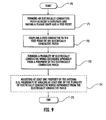
- a method aspect is directed to a method for making a patch antenna 10.
- the method begins (block 70) and includes forming an electrically conductive patch 12 adjacent a dielectric substrate 14 and having a planar shape and a feed point 15 defined therein (block 71).
- the method includes coupling a feed conductor 20 to the feed point 15 of the electrically conductive patch 12.
- the method includes forming a plurality of electrically conductive wings 16 extending upwardly from a periphery of the electrically conductive patch 12 (block 73).
- the periphery of the electrically conductive base 12 may have a polygonal shape defining a plurality of linear segments L and associated vertices V, and wherein forming the plurality of electrically conductive wings 16 (at block 73) comprises forming a respective electrically conductive wing 16 extending upwardly from each linear segment L. Forming the plurality of electrically conductive wings 16 may comprise forming each to have at least one triangular shaped portion 30.
- the method may additionally include adjusting at least one property of the patch antenna 50 by angling at least one of the plurality of electrically conductive wings 56 outwardly from the electrically conductive patch 52 before ending at block 75.
- a broadband patch antenna is described above including the use of batwing and bowtie tabs that form broadband dipoles. Tuning and production trimming are included, and circular polarization may be provided.
- the patch antenna type is ubiquitous for GPS and personal communications, e.g. LTE mobile data.
- the planar patch antenna is flexible and scalable as to frequency, and provides adequate gain and wide bandwidth, for many modes and sizes of patch antennas.
Abstract
Description
- The present invention relates to the field of wireless communications, and, more particularly, to antennas and related methods.
- Newer designs and manufacturing techniques have driven electronic components to small dimensions and miniaturized many communication devices and systems. Unfortunately, antennas have not been reduced in size at a comparative level and often are one of the larger components used in a smaller communications device. It becomes increasingly important in communication applications to reduce not only antenna size, but also to design and manufacture a scalable size antenna having sufficient gain on the frequency needed. Accurate antenna tuning is important for small narrowband antennas.
- In current, everyday communications devices, many different types of patch antennas, loaded whips, copper springs (coils and pancakes) and dipoles are used in a variety of different ways. These antennas, however, are sometimes large and impractical for a specific application. Antennas having diverging electric currents may be called dipoles, those having curling electric currents may be loops, and dipole-loop hybrids may comprise the helix and spiral. While dipole antennas can be thin linear or "1 dimensional" in shape, loop antennas are at least 2 dimensional. Loop antennas can be a good fit for planar requirements.
- Antennas can of course assume many geometric shapes. The Euclidian geometries are sometimes preferential for antennas as they convey optimizations known through the ages. For instance, line shaped dipoles may have the shortest distance between two points, and circular loop antennas may have the most enclosed area for the least circumference. So, both line and circle shapes may minimize antenna conductor length to increase radiation efficiency. Yet line and circle shaped antennas may not meet all needs, such as operation at small physical size relative wavelength and a self loading antenna structure may be needed, such as a helix or spiral antenna.
- Simple flat or patch antennas can be manufactured as printed circuit boards (PCBs) at low costs and have been developed as antennas for the mobile communication field. The microstrip patch antenna is configured, for example, by disposing a patch conductor cut to a predetermined size over a conductive "ground" plate through a dielectric material. An elegant compound design results: one or more patch edges may radiate as slot antennas, a transmission line impedance matching transformer is obtained, unidirection radiation can be provided, and patch sizing allows synthesis of radiation pattern shapes. The patch may even be excited for linear, circular, and dual polarizations polarizations. Patch efficiency may exceed 90%. For comparision, parabolic reflectors may operate at only 50 to 80 percent efficiency, due to factors of feed spillover, non uniform aperture illumination, and surface tolerances. In fact few or no antennas exceed patch antennas in realized gain for area. Patch arrays may exceed Gr > 10 log10 [(0.9)4πa/λ2], where Gr is realized gain in dBi, a is the area of the patches in square meters, and λ is the free space wavelength in meters.
- However, microstrip patch antennas typically are efficient only in a narrow frequency band. They are poorly shaped for wave expansion, such that microstrip antenna bandwidth is proportional to antenna thickness. Bandwidth can even approach zero with vanishing thickness (for example, see Munson, page 7-8 "Antenna Engineering Handbook", 2nd ed., H. Jasik ed.). Limitations of narrow instantaneous radiation bandwidth are potentiated by any variation in PWB substrate dielectric constant; tuning drift may cause the high gain may be unavailable on the frequency needed. This can be problematic when high dielectric constant substrates are used: the miniaturized patch has less fixed tuned bandwidth to mitigate tuning errors, yet high dielectric constant materials typically have wider dielectric constant variations. The typical microstrip patch antenna may not support the whole 1500-1700 MHz mobile satcom band, for example. It also includes sensitive tuning tolerances and production frequency trimming is upwards only (e.g. via patch ablation). Patch resonant frequency is inversely proportional to the square root of substrate dielectric constant (f ∼ 1/√εr).
-
U.S. Pat. No. 6,501,427 to Lilly et al. entitled "Tunable Patch Antenna" is directed to a patch antenna including a segmented patch and reed like MEMS switches on a substrate. Segments of the structure can be switched to reconfigure the antenna, providing a broad tunable bandwidth. Instantaneous bandwidth may be unaffected however. -
U.S. Pat. No. 7,126,538 to Sampo entitled "Microstrip Antenna" is directed to a microstrip antenna with a dielectric member disposed on a grounded conductive plate. A patch antenna element is disposed on the dielectric member. -
U.S. Pat. No. 7,495,627 to Parsche entitled "Broadband Planar Dipole Antenna Structure And Associated Methods" describes a planar dipole-circular microstrip patch antenna with increased instantaneous gain bandwidth by polynomial tuning. -
U.S. Pat. No. 7,432,862 to Heyde is directed to a broadband patch antenna including a planar metallic patch sheet that is provided with right-angled edges.U.S. Pat. No. 6,606,601 to Wong et al . is directed to a broadband circularly polarized patch antenna including an L-shaped ground plane consisting of a vertical ground plane and a horizontal ground plane, a radiating metal patch, a probe feed placed coplanarly with the radiating metal patch and connected to the radiating metal patch through the vertical ground plane, and a substrate between the radiating metal patch and the horizontal ground plane. - There may be a desire for a planar patch antenna that may be flexible and/or scalable as to frequency, and provide adequate gain and wide bandwidth.
- In view of the foregoing background, it is therefore an object of the present invention to provide a broadband and/or tunable patch antenna.
- This and other objects, features, and advantages in accordance with the present invention are provided by a patch antenna including a substrate, an electrically conductive patch carried by the substrate and having a planar shape and a feed point defined therein, a feed conductor coupled to the feed point of the electrically conductive patch, and a plurality of electrically conductive wings extending upwardly from a periphery of the electrically conductive patch.
- The periphery of the electrically conductive patch may have a polygonal shape defining a plurality of linear segments and associated vertices. The plurality of electrically conductive wings may comprise a respective electrically conductive wing extending upwardly from each linear segment. Each of the plurality of electrically conductive wings may comprise at least one triangular shaped portion. Each of the plurality of electrically conductive wings may comprise a triangular shaped portion with a base extending along a respective linear segment, and an apex opposite the base.
- Each of the plurality of electrically conductive wings may comprise first and second right angle triangular shaped portions each with a leg extending upward from a respective vertex and a hypotenuse extending to a common medial position along a respective linear segment. The polygonal shape may comprise a rectangular shape. At least one of the plurality of electrically conductive wings may be angled outwardly from the electrically conductive patch. Also, a ground plane and a dielectric layer may be between the substrate and the electrically conductive patch.
- A method aspect is directed to a method for making a patch antenna including forming an electrically conductive patch adjacent a substrate and having a planar shape and a feed point defined therein, coupling a feed conductor to the feed point of the electrically conductive patch, and forming a plurality of electrically conductive wings extending upwardly from a periphery of the electrically conductive patch.
- The periphery of the electrically conductive base may have a polygonal shape defining a plurality of linear segments and associated vertices, and wherein forming the plurality of electrically conductive wings comprises forming a respective electrically conductive wing extending upwardly from each linear segment. Forming the plurality of electrically conductive wings may comprise forming each to have at least one triangular shaped portion. The method may include adjusting at least one property of the antenna by angling at least one of the plurality of electrically conductive wings outwardly from the electrically conductive patch.
-
-
FIG. 1 is a perspective view of an embodiment of a patch antenna in accordance with the present invention. -
FIG. 2 is a side view of the patch antenna ofFIG. 1 . -
FIG. 3 is a graph of frequency and gain for a patch antenna according to the prior art. -
FIG. 4 is a graph of frequency and gain for the patch antenna ofFIG. 1 . -
FIG. 5 is a perspective view of another embodiment of a patch antenna in accordance with the present invention. -
FIGs. 6A and 6B are views of the patch antenna ofFIG. 5 and illustrating a tuning feature. -
FIG. 6C is a graph of frequency and bend angle for the patch antenna ofFIG. 5 . -
FIG. 7 is a schematic diagram of an embodiment of a square patch antenna in accordance with the present invention. -
FIG. 8 is a schematic diagram of an embodiment of a circular patch antenna in accordance with the present invention. -
FIG. 9 is a flowchart illustrating an embodiment of a method in accordance with features of the present invention. - The present invention will now be described more fully hereinafter with reference to the accompanying drawings, in which preferred embodiments of the invention are shown. This invention may, however, be embodied in many different forms and should not be construed as limited to the embodiments set forth herein. Rather, these embodiments are provided so that this disclosure will be thorough and complete, and will fully convey the scope of the invention to those skilled in the art. Like numbers refer to like elements throughout.
- Referring initially to
FIGs. 1 and2 , an embodiment of apatch antenna 10 in accordance with features of the present invention will be described. Thepatch antenna 10 includes an electricallyconductive patch 12, e.g. carried by adielectric substrate 14, and having a planar shape and afeed point 15 defined therein. Afeed conductor 20 is coupled to thefeed point 15 of the electricallyconductive patch 12. Thedielectric substrate 14 may one or more materials such as Teflon, a magnetic substrate such as ferrite, a plastic foam, honeycomb structure, or even air. - Also, a
ground plane 18 may be adjacent thedielectric substrate 14 and the electricallyconductive patch 12. As illustrated inFIG. 2 ,such feed connector 20 may be a coaxial connector including andouter conductor 21 coupled to theground plane 18, and aninner conductor 22 coupled to thefeed point 15. - A plurality of electrically
conductive wings 16 extend upwardly from a periphery of the electricallyconductive patch 12. Such electricallyconductive wings 16 may be characterized as batwings. The edges of the electricallyconductive patch 12, including the electricallyconductive wings 16 may electrically constitute batwing slot dipoles. - The periphery of the electrically
conductive patch 12 may have a polygonal shape, e.g. a rectangular or square shape, defining a plurality of linear segments L and associated vertices V. The plurality of electricallyconductive wings 16 may comprise a respective electricallyconductive wing 16 extending upwardly from each linear segment L. Each of the plurality of electricallyconductive wings 16 may comprise at least one triangular shapedportion 30. Each of the plurality of electricallyconductive wings 16 may comprise a triangular shapedportion 30 with a base B extending along a respective linear segment L, and an apex A opposite the base. For broadside radiation the perimeter of asquare patch 12 may be between about 1.5 and 1.95 guide wavelengths in perimeter at resonance, e.g. 1.52λair√εr < p < 2λair√εr, where p is the perimeter around the square patch element, λair is the wavelengths in air, and εr is the relative permittivity of the dielectric substrate. Of course, the electricallyconductive patch 12 may be other sizes and shapes such as rectangular or circular. The tradeoffs between broadside firing square and circular patches include: square patches are somewhat larger in size than the circular patches for the same resonant frequency; square patches provide about 1 dB more gain than the circle shaped patches; square patches provide more total instantaneous bandwidth than the circle; circle patches give more instantaneous bandwidth per area than the square. - Each of the plurality of electrically
conductive wings 16 may comprise first and second right angle triangular shapedportions 30 each with aleg 31 extending upward from a respective vertex V and a hypotenuse 32 extending to a commonmedial position 33 along a respective linear segment L. - Gain responses with and without the plurality of electrically
conductive wings 16 will now be described.FIG. 3 ,trace 90 is the response of the square patch ofFIG. 1 including the electricallyconductive wings 16, which at that time were standing straight up from (and therefore perpendicular to the plane of) thepatch antenna 10.FIG. 4 ,trace 92 is the same antenna response without the electricallyconductive wings 16. As can be seen, the wings caused a 9.5% downward shift of thepeak gain frequencies - Referring now to
FIGs. 5 ,6A and 6B , another embodiment of apatch antenna 50 in accordance with features of the present invention will be described. Thepatch antenna 50 includes an electricallyconductive patch 52, e.g. carried by adielectric substrate 54, and having a planar shape and afeed point 55 defined therein. A feed conductor may coupled to thefeed point 55 of the electricallyconductive patch 52. A plurality of electricallyconductive wings 56 extend upwardly from a periphery of the electricallyconductive patch 52. Such electricallyconductive wings 56 may be characterized as bowtie wings. - The periphery of the electrically
conductive patch 52 may have a polygonal shape, e.g. a rectangular or square shape, or a trapezoidal shape as shown, defining a plurality of linear segments L and associated vertices V. The plurality of electricallyconductive wings 56 may comprise a respective electricallyconductive wing 56 extending upwardly from each linear segment L. Each of the plurality of electricallyconductive wings 56 may comprise at least one triangular shapedportion 60. Each of the plurality of electricallyconductive wings 56 may comprise a triangular shapedportion 60 with a base B extending along a respective linear segment L, and an apex A opposite the base. At least one of the plurality of electricallyconductive wings 56 may be angled outwardly from the electricallyconductive patch 52. - The bend angle α of the electrically
conductive wings 56 may be changed to adjust the frequency of each edge of the electricallyconductive patch 52, e.g. as illustrated in the graph ofFIG. 6C . Bend angle α is 0 degrees when the electricallyconductive wings 56 are flat against the printed circuit board, and 90 degrees when the electricallyconductive wings 56 are perpendicular. The frequency may be increased by bending the respective electricallyconductive wing 56 upwardly away from the patch plane, or decreased by bending such electricallyconductive wing 56 downwardly towards the patch plane. For example, a frequency adjustment range of +/- 12% may be obtained via the bending angle of the electricallyconductive wings 56. - As the electrically
conductive wings 56 may cause a downward frequency shift, even when the wings are straight up (bend angle α 90°), a method of using the electricallyconductive wings 16 is to downsize the electricallyconductive patch 12 prior to receiving electricallyconductive wings 16. So, the electricallyconductive patch 12 may be tuned upwards by patch size reduction prior to receiving the electricallyconductive wings 16. One way to do this is by patch ablation. Of course, the electricallyconductive patch 12 and electricallyconductive wings 16 may alternatively be designed together or even fabricated together as a single part. - The electrically
conductive wings 56 may be formed or implemented in many ways. One method to implement the electricallyconductive wings 56 is to manufacture the electricallyconductive wings 56 and thepatch 52 separately. In this case the electrically conductive wings may be stamped sheet metal, the patch a printed wiring board feature formed by milling or etching, and the wings subsequently joined to the patch by soldering. Another way to provide the electricallyconductive wings 56 is to form the electricallyconductive wings 56 and thepatch 52 at the same time, e.g. from a common sheet metal stamping. - A method of the invention is to synthesize circular polarized radiation using the electrically conductive wings. Illustratrating this method, the
FIG. 7 diagram 102 depicts asquare microstrip patch 104 antenna with four adjustable electrically conductive wings, denoted by position as +X, +Y, -X, -Y. Each of the four adjustable electrically conductive wings +X, +Y, -X, -Y permits independent adjustment of resonance frequency for that radiating patch edge.Patch 104 may be suspended over a ground plane using a dielectric layer, but these features are not shown for clarity.Electrical feed pin 106 may excite the patch at a point along either of the imaginary diagonals depicted as a dashedlines -
Patch 104 is made square (all edges equal length of course) and the patch edges may be at fundamental resonance between 0.4 to 0.5 wavelengths long electrically, e.g. 0.4c/f√εr < L < 0.4c/f√εr meters, L is the edge length in meters, c is the speed of light in meters/second, f is the operating frequency in Hertz, and εr is the real part of the substrate relative permittivity, which is a dimensionless number. This patch size provides broadside radiation normal to the patch plane. For illustration, all of the adjustable electrically conductive wings initially have the same bend angle α, e.g. 45 degrees. Now, to synthesize right hand circular polarization in the +Z direction: 1) the +X and -X adjustable electrically conductive wings are adjusted downward towards the patch plane slightly, while 2) the +Y and -Y adjustable electrically conductive wings are adjusted upwards away from the patch plane slightly. The effect of these wing adjustments is to cause the +X, -X radiating edges to be resonant slightly lower than the operating frequency, and the +Y, -Y edges to be resonant slightly higher than the operating frequency. Radiation from the +X, -X radiating edges will now lag somewhat in phase and radiation from the +Y, -Y radiating edges will lead somewhat in phase. Quantatively, for perfectly circular right hand circular polarization the wings are adjusted such that the +X, -X radiating edges are 45 degrees lagging in phase, and the +Y, -Y radiating edges are 45 degrees leading in phase. The resulting 90 degree phase difference between the orthogonal radiating edges is sufficient to cause the circular polarization wave rotation. Differences between +X, -X edge resonate frequency and +Y, -Y resonate frequency to accomplish this may be small, between about 0.5 to 4 percent. - Polarization bandwidth from this method is narrow but the VSWR bandwidth is increased, about double. The resulting circular polarization VSWR response will have two minima on either side of the operating frequency, and a center rise, like a 4th order Chebyschev filter response. Without the circular polarization synthesis the VSWR response is quadratic with only one minima. This method can supply any rotational polarization, circular or elliptical. Elliptical polarization may be obtained by moving the feed point off the diagonals to unequally power the radiating edges. It is understood here that when rotational polarization is recited, both circular and elliptical polarization are being referred to here.
- Special considerations apply to the use of circular shaped microstrip patch elements used for circular polarization. Unlike the square and rectangular patch, circular polarization from circular patch elements by unequal edge resonances may not be practical: separate, uncoupled radiating edges are not present on a circle. While linearly polarized circular patch antennas have standing wave current distributions, circularly polarized patch antennas have traveling wave current distributions. So, the circular shaped circularly polarized patch may have current maxima (lumps of current) rotating around the patch periphery at a rate of ω = 2nf rotations/second. Typically, the number of current lumps that form is two, regardless of circular patch size.
- Referring to
FIG. 8 then, a practical circularly polarized circularelement patch antenna 122 utilizingconductive wings FIG. 8 example depicts a method of the invention for utilizing conductive wings on circularly polarized circular element patch antennas. In theFIG. 8 example the patch circumference C is about 1.76 wavelengths in dielectric , e.g. C = 1.76√g = 1.76 λair / √εr = 1.76c/f√εr. A ground plane may be present but not depicted. Here twofeed pins -
Conductive wings patch 122 center and the drive pins 128, 130. A single conductive wing (not used or depicted) would disrupt circularly polarized circular patch operation due to perturbation of the surface waves that attach and rotating about the patch periphery; reflections from a single wing alone would result in a countersense traveling wave current that would buck the radiation from the desired sense traveling wave current. However, in theFIG. 8 geometry twoconductive wings - Equal surface wave perturbations do occur from each
conductive wing conductive wings FIG. 8 are therefore made equal in size, shape, and bend angle α. TheFIG. 8 embodiment advantageously may allow frequency trimming of circular patch antennas, e.g. to mitigate dielectric variations in unit production. The method includes adjusting the two electricallyconductive wings - Referring additionally to the flowchart of
FIG. 8 , a method aspect is directed to a method for making apatch antenna 10. The method begins (block 70) and includes forming an electricallyconductive patch 12 adjacent adielectric substrate 14 and having a planar shape and afeed point 15 defined therein (block 71). Atblock 72, the method includes coupling afeed conductor 20 to thefeed point 15 of the electricallyconductive patch 12. Further, the method includes forming a plurality of electricallyconductive wings 16 extending upwardly from a periphery of the electrically conductive patch 12 (block 73). - The periphery of the electrically
conductive base 12 may have a polygonal shape defining a plurality of linear segments L and associated vertices V, and wherein forming the plurality of electrically conductive wings 16 (at block 73) comprises forming a respective electricallyconductive wing 16 extending upwardly from each linear segment L. Forming the plurality of electricallyconductive wings 16 may comprise forming each to have at least one triangular shapedportion 30. - The method (at block 74) may additionally include adjusting at least one property of the
patch antenna 50 by angling at least one of the plurality of electricallyconductive wings 56 outwardly from the electricallyconductive patch 52 before ending atblock 75. - Accordingly, a broadband patch antenna is described above including the use of batwing and bowtie tabs that form broadband dipoles. Tuning and production trimming are included, and circular polarization may be provided. The patch antenna type is ubiquitous for GPS and personal communications, e.g. LTE mobile data. The planar patch antenna is flexible and scalable as to frequency, and provides adequate gain and wide bandwidth, for many modes and sizes of patch antennas.
- Many modifications and other embodiments of the invention will come to the mind of one skilled in the art having the benefit of the teachings presented in the foregoing descriptions and the associated drawings. Therefore, it is understood that the invention is not to be limited to the specific embodiments disclosed, and that modifications and embodiments are intended to be included within the scope of the appended claims.
Claims (10)
- A patch antenna comprising:a substrate;an electrically conductive patch carried by said substrate and having a planar shape and a feed point defined therein;a feed conductor coupled to the feed point of said electrically conductive patch; anda plurality of electrically conductive wings extending upwardly from a periphery of said electrically conductive patch.
- The patch antenna according to Claim 1
wherein the periphery of said electrically conductive patch has a polygonal shape defining a plurality of linear segments and associated vertices. - The patch antenna according to Claim 2
wherein said plurality of electrically conductive wings comprises a respective electrically conductive wing extending upwardly from each linear segment. - The patch antenna according to Claim 2
wherein each of said plurality of electrically conductive wings comprises at least one triangular shaped portion. - The patch antenna according to Claim 2
wherein each of said plurality of electrically conductive wings comprises a triangular shaped portion with a base extending along a respective linear segment, and an apex opposite the base. - The patch antenna according to Claim 2
wherein each of said plurality of electrically conductive wings comprises first and second right angle triangular shaped portions each with a leg extending upward from a respective vertex and a hypotenuse extending to a common medial position along a respective linear segment. - A method for making a patch antenna comprising:forming an electrically conductive patch adjacent a substrate and having a planar shape and a feed point defined therein;coupling a feed conductor to the feed point of the electrically conductive patch; andforming a plurality of electrically conductive wings extending upwardly from a periphery of the electrically conductive patch.
- The method according to Claim 7 wherein the periphery of the electrically conductive base has a polygonal shape defining a plurality of linear segments and associated vertices; and wherein forming the plurality of electrically conductive wings comprises forming a respective electrically conductive wing extending upwardly from each linear segment.
- The method according to Claim 8 wherein forming the plurality of electrically conductive wings comprises forming each to have at least one triangular shaped portion.
- The method according to Claim 8 further comprising adjusting at least one property of the antenna by angling at least one of the plurality of electrically conductive wings outwardly from the electrically conductive patch.
Applications Claiming Priority (1)
| Application Number | Priority Date | Filing Date | Title |
|---|---|---|---|
| US14/105,454 US9748656B2 (en) | 2013-12-13 | 2013-12-13 | Broadband patch antenna and associated methods |
Publications (2)
| Publication Number | Publication Date |
|---|---|
| EP2884585A1 true EP2884585A1 (en) | 2015-06-17 |
| EP2884585B1 EP2884585B1 (en) | 2017-06-14 |
Family
ID=52272797
Family Applications (1)
| Application Number | Title | Priority Date | Filing Date |
|---|---|---|---|
| EP14004195.5A Active EP2884585B1 (en) | 2013-12-13 | 2014-12-12 | Broadband patch antenna and associated methods |
Country Status (2)
| Country | Link |
|---|---|
| US (1) | US9748656B2 (en) |
| EP (1) | EP2884585B1 (en) |
Families Citing this family (2)
| Publication number | Priority date | Publication date | Assignee | Title |
|---|---|---|---|---|
| US11329384B2 (en) * | 2020-01-21 | 2022-05-10 | Embry-Riddle Aeronautical University, Inc. | Z-axis meandering patch antenna and fabrication thereof |
| EP4260404A1 (en) * | 2020-12-11 | 2023-10-18 | Google LLC | Dual-band patch antenna for angle-of-arrival analysis |
Citations (9)
| Publication number | Priority date | Publication date | Assignee | Title |
|---|---|---|---|---|
| US5200756A (en) * | 1991-05-03 | 1993-04-06 | Novatel Communications Ltd. | Three dimensional microstrip patch antenna |
| US6501427B1 (en) | 2001-07-31 | 2002-12-31 | E-Tenna Corporation | Tunable patch antenna |
| US6606601B1 (en) | 1999-10-16 | 2003-08-12 | Mary Joan Willard | Distance delivery of vocational services coupled with shared payments from third party payers |
| US7126538B2 (en) | 2003-09-29 | 2006-10-24 | Yokowo Co., Ltd. | Microstrip antenna |
| EP1760833A1 (en) * | 2004-06-25 | 2007-03-07 | Sony Corporation | Antenna and radio communication unit |
| US7432862B2 (en) | 2004-06-23 | 2008-10-07 | Huber + Suhner Ag | Broadband patch antenna |
| US7495627B2 (en) | 2007-06-14 | 2009-02-24 | Harris Corporation | Broadband planar dipole antenna structure and associated methods |
| US20110012788A1 (en) * | 2009-07-14 | 2011-01-20 | Hong Kong Applied Science And Technology Research Institute Co., Ltd. | Miniature Circularly Polarized Folded Patch Antenna |
| US20110050529A1 (en) * | 2007-01-30 | 2011-03-03 | Fraunhofer-Gesellschaft Zur Foerderung Der Angewandten Forschung E. V. | Antenna device for transmitting and receiving electromegnetic signals |
Family Cites Families (23)
| Publication number | Priority date | Publication date | Assignee | Title |
|---|---|---|---|---|
| US2480153A (en) | 1945-01-27 | 1949-08-30 | Rca Corp | Antenna |
| US5442366A (en) * | 1993-07-13 | 1995-08-15 | Ball Corporation | Raised patch antenna |
| DE69423939T2 (en) | 1993-08-20 | 2000-10-19 | Raytheon Co | Antennas |
| US5502451A (en) | 1994-07-29 | 1996-03-26 | The United States Of America As Represented By The Secretary Of The Air Force | Patch antenna with magnetically controllable radiation polarization |
| US6128471A (en) | 1995-08-21 | 2000-10-03 | Nortel Networks Corporation | Telecommunication method and system for communicating with multiple terminals in a building through multiple antennas |
| US5943016A (en) | 1995-12-07 | 1999-08-24 | Atlantic Aerospace Electronics, Corp. | Tunable microstrip patch antenna and feed network therefor |
| US5777581A (en) | 1995-12-07 | 1998-07-07 | Atlantic Aerospace Electronics Corporation | Tunable microstrip patch antennas |
| SE505796C2 (en) * | 1996-01-19 | 1997-10-13 | Ericsson Telefon Ab L M | Double polarized antenna |
| SE508513C2 (en) * | 1997-02-14 | 1998-10-12 | Ericsson Telefon Ab L M | Microstrip antenna as well as group antenna |
| US6118406A (en) | 1998-12-21 | 2000-09-12 | The United States Of America As Represented By The Secretary Of The Navy | Broadband direct fed phased array antenna comprising stacked patches |
| US6239751B1 (en) | 1999-09-14 | 2001-05-29 | Ball Aerospace & Technologies Corp. | Low profile tunable antenna |
| US6292143B1 (en) | 2000-05-04 | 2001-09-18 | The United States Of America As Represented By The Administrator Of The National Aeronautics And Space Administration | Multi-mode broadband patch antenna |
| US6342857B1 (en) | 2000-09-01 | 2002-01-29 | Auden Techno Corp. | Broadband circuit shorted resonant patch antenna |
| JP2004520745A (en) | 2001-02-07 | 2004-07-08 | フラクトゥス・ソシエダッド・アノニマ | Small Broadband / Ring / Microstrip Patch Antenna |
| TW518802B (en) | 2001-10-03 | 2003-01-21 | Accton Technology Corp | Broadband circularly polarized panel antenna |
| FR2841688B1 (en) | 2002-06-28 | 2006-06-30 | Antennes Ft | PATCH TYPE FLAT ANTENNA, IN PARTICULAR FOR TRANSMITTING AND / OR RECEIVING DIGITAL AND / OR ANALOGUE TERRESTRIAL TELEVISION SIGNALS |
| US7079078B2 (en) * | 2003-04-09 | 2006-07-18 | Alps Electric Co., Ltd. | Patch antenna apparatus preferable for receiving ground wave and signal wave from low elevation angle satellite |
| US7741999B2 (en) | 2006-06-15 | 2010-06-22 | Kathrein-Werke Kg | Multilayer antenna of planar construction |
| JP4692789B2 (en) * | 2007-04-27 | 2011-06-01 | 日本電気株式会社 | Patch antenna with metal wall |
| US7808441B2 (en) * | 2007-08-30 | 2010-10-05 | Harris Corporation | Polyhedral antenna and associated methods |
| US7952528B2 (en) | 2007-09-04 | 2011-05-31 | Sierra Wireless, Inc. | Antenna configurations for compact device wireless communication |
| US7916090B2 (en) | 2007-09-04 | 2011-03-29 | Sierra Wireless, Inc. | Antenna configurations for compact device wireless communication |
| US7928913B2 (en) | 2008-08-20 | 2011-04-19 | Alcatel-Lucent Usa Inc. | Method and apparatus for a tunable channelizing patch antenna |
-
2013
- 2013-12-13 US US14/105,454 patent/US9748656B2/en active Active
-
2014
- 2014-12-12 EP EP14004195.5A patent/EP2884585B1/en active Active
Patent Citations (9)
| Publication number | Priority date | Publication date | Assignee | Title |
|---|---|---|---|---|
| US5200756A (en) * | 1991-05-03 | 1993-04-06 | Novatel Communications Ltd. | Three dimensional microstrip patch antenna |
| US6606601B1 (en) | 1999-10-16 | 2003-08-12 | Mary Joan Willard | Distance delivery of vocational services coupled with shared payments from third party payers |
| US6501427B1 (en) | 2001-07-31 | 2002-12-31 | E-Tenna Corporation | Tunable patch antenna |
| US7126538B2 (en) | 2003-09-29 | 2006-10-24 | Yokowo Co., Ltd. | Microstrip antenna |
| US7432862B2 (en) | 2004-06-23 | 2008-10-07 | Huber + Suhner Ag | Broadband patch antenna |
| EP1760833A1 (en) * | 2004-06-25 | 2007-03-07 | Sony Corporation | Antenna and radio communication unit |
| US20110050529A1 (en) * | 2007-01-30 | 2011-03-03 | Fraunhofer-Gesellschaft Zur Foerderung Der Angewandten Forschung E. V. | Antenna device for transmitting and receiving electromegnetic signals |
| US7495627B2 (en) | 2007-06-14 | 2009-02-24 | Harris Corporation | Broadband planar dipole antenna structure and associated methods |
| US20110012788A1 (en) * | 2009-07-14 | 2011-01-20 | Hong Kong Applied Science And Technology Research Institute Co., Ltd. | Miniature Circularly Polarized Folded Patch Antenna |
Non-Patent Citations (1)
| Title |
|---|
| MUNSON: "Antenna Engineering Handbook", pages: 7 - 8 |
Also Published As
| Publication number | Publication date |
|---|---|
| US9748656B2 (en) | 2017-08-29 |
| EP2884585B1 (en) | 2017-06-14 |
| US20150171520A1 (en) | 2015-06-18 |
Similar Documents
| Publication | Publication Date | Title |
|---|---|---|
| JP5284491B2 (en) | Half-loop chip antenna and related methods | |
| Chang et al. | Compact multi-band H-shaped slot antenna | |
| Shi et al. | Wideband and low-profile omnidirectional circularly polarized antenna with slits and shorting-vias | |
| TWI489690B (en) | Multi-band planar inverted-f (pifa) antennas and systems with improved isolation | |
| Mak et al. | A shorted bowtie patch antenna with a cross dipole for dual polarization | |
| Rezaeieh et al. | Miniaturization of planar Yagi antennas using mu-negative metamaterial-loaded reflector | |
| JP2004088218A (en) | Planar antenna | |
| US9799956B2 (en) | Three-dimensional compound loop antenna | |
| Tran et al. | A compact wideband omnidirectional circularly polarized antenna using TM 01 mode with capacitive feeding | |
| CN106486741B (en) | Air patch microstrip antenna | |
| JP2004266333A (en) | Antenna device | |
| JP6456506B2 (en) | Antenna device | |
| Yang et al. | A novel single feed omnidirectional circularly polarized antenna with wide AR bandwidth | |
| EP2884585B1 (en) | Broadband patch antenna and associated methods | |
| US11050151B2 (en) | Multi-band antenna | |
| Luo et al. | Circularly polarized substrate integrated waveguide antenna with wide axial-ratio beamwidth | |
| US11063357B2 (en) | Dual-band antenna for global positioning system | |
| Ahsan et al. | Slot loaded rectangular patch antenna for dual-band operations on glass-reinforced epoxy laminated inexpensive substrate | |
| Ta et al. | Dual-band operation of a circularly polarized four-arm curl antenna with asymmetric arm length | |
| KR101096461B1 (en) | Monopole Chip Antenna using Ground Path in 2.4GHz | |
| Ding et al. | A novel loop-like monopole antenna with dual-band circular polarization | |
| Reddy et al. | Fabrication of patch antenna with circular polarization for wireless LAN applications | |
| US20140333501A1 (en) | Ultrabroadband antenna | |
| US11088455B2 (en) | Spiral wideband low frequency antenna | |
| Lin et al. | A novel circular-polarization-switchable slot ring antenna with diagonal cross slit |
Legal Events
| Date | Code | Title | Description |
|---|---|---|---|
| PUAI | Public reference made under article 153(3) epc to a published international application that has entered the european phase |
Free format text: ORIGINAL CODE: 0009012 |
|
| 17P | Request for examination filed |
Effective date: 20141212 |
|
| AK | Designated contracting states |
Kind code of ref document: A1 Designated state(s): AL AT BE BG CH CY CZ DE DK EE ES FI FR GB GR HR HU IE IS IT LI LT LU LV MC MK MT NL NO PL PT RO RS SE SI SK SM TR |
|
| AX | Request for extension of the european patent |
Extension state: BA ME |
|
| GRAP | Despatch of communication of intention to grant a patent |
Free format text: ORIGINAL CODE: EPIDOSNIGR1 |
|
| STAA | Information on the status of an ep patent application or granted ep patent |
Free format text: STATUS: GRANT OF PATENT IS INTENDED |
|
| INTG | Intention to grant announced |
Effective date: 20161128 |
|
| GRAS | Grant fee paid |
Free format text: ORIGINAL CODE: EPIDOSNIGR3 |
|
| GRAJ | Information related to disapproval of communication of intention to grant by the applicant or resumption of examination proceedings by the epo deleted |
Free format text: ORIGINAL CODE: EPIDOSDIGR1 |
|
| GRAL | Information related to payment of fee for publishing/printing deleted |
Free format text: ORIGINAL CODE: EPIDOSDIGR3 |
|
| STAA | Information on the status of an ep patent application or granted ep patent |
Free format text: STATUS: REQUEST FOR EXAMINATION WAS MADE |
|
| INTC | Intention to grant announced (deleted) | ||
| GRAR | Information related to intention to grant a patent recorded |
Free format text: ORIGINAL CODE: EPIDOSNIGR71 |
|
| STAA | Information on the status of an ep patent application or granted ep patent |
Free format text: STATUS: GRANT OF PATENT IS INTENDED |
|
| GRAA | (expected) grant |
Free format text: ORIGINAL CODE: 0009210 |
|
| STAA | Information on the status of an ep patent application or granted ep patent |
Free format text: STATUS: THE PATENT HAS BEEN GRANTED |
|
| INTG | Intention to grant announced |
Effective date: 20170504 |
|
| AK | Designated contracting states |
Kind code of ref document: B1 Designated state(s): AL AT BE BG CH CY CZ DE DK EE ES FI FR GB GR HR HU IE IS IT LI LT LU LV MC MK MT NL NO PL PT RO RS SE SI SK SM TR |
|
| REG | Reference to a national code |
Ref country code: GB Ref legal event code: FG4D |
|
| REG | Reference to a national code |
Ref country code: CH Ref legal event code: EP Ref country code: AT Ref legal event code: REF Ref document number: 901774 Country of ref document: AT Kind code of ref document: T Effective date: 20170615 |
|
| REG | Reference to a national code |
Ref country code: IE Ref legal event code: FG4D |
|
| REG | Reference to a national code |
Ref country code: DE Ref legal event code: R096 Ref document number: 602014010638 Country of ref document: DE |
|
| REG | Reference to a national code |
Ref country code: NL Ref legal event code: MP Effective date: 20170614 |
|
| REG | Reference to a national code |
Ref country code: LT Ref legal event code: MG4D |
|
| PG25 | Lapsed in a contracting state [announced via postgrant information from national office to epo] |
Ref country code: GR Free format text: LAPSE BECAUSE OF FAILURE TO SUBMIT A TRANSLATION OF THE DESCRIPTION OR TO PAY THE FEE WITHIN THE PRESCRIBED TIME-LIMIT Effective date: 20170915 Ref country code: HR Free format text: LAPSE BECAUSE OF FAILURE TO SUBMIT A TRANSLATION OF THE DESCRIPTION OR TO PAY THE FEE WITHIN THE PRESCRIBED TIME-LIMIT Effective date: 20170614 Ref country code: LT Free format text: LAPSE BECAUSE OF FAILURE TO SUBMIT A TRANSLATION OF THE DESCRIPTION OR TO PAY THE FEE WITHIN THE PRESCRIBED TIME-LIMIT Effective date: 20170614 Ref country code: FI Free format text: LAPSE BECAUSE OF FAILURE TO SUBMIT A TRANSLATION OF THE DESCRIPTION OR TO PAY THE FEE WITHIN THE PRESCRIBED TIME-LIMIT Effective date: 20170614 Ref country code: NO Free format text: LAPSE BECAUSE OF FAILURE TO SUBMIT A TRANSLATION OF THE DESCRIPTION OR TO PAY THE FEE WITHIN THE PRESCRIBED TIME-LIMIT Effective date: 20170914 |
|
| REG | Reference to a national code |
Ref country code: AT Ref legal event code: MK05 Ref document number: 901774 Country of ref document: AT Kind code of ref document: T Effective date: 20170614 |
|
| PG25 | Lapsed in a contracting state [announced via postgrant information from national office to epo] |
Ref country code: SE Free format text: LAPSE BECAUSE OF FAILURE TO SUBMIT A TRANSLATION OF THE DESCRIPTION OR TO PAY THE FEE WITHIN THE PRESCRIBED TIME-LIMIT Effective date: 20170614 Ref country code: RS Free format text: LAPSE BECAUSE OF FAILURE TO SUBMIT A TRANSLATION OF THE DESCRIPTION OR TO PAY THE FEE WITHIN THE PRESCRIBED TIME-LIMIT Effective date: 20170614 Ref country code: NL Free format text: LAPSE BECAUSE OF FAILURE TO SUBMIT A TRANSLATION OF THE DESCRIPTION OR TO PAY THE FEE WITHIN THE PRESCRIBED TIME-LIMIT Effective date: 20170614 Ref country code: BG Free format text: LAPSE BECAUSE OF FAILURE TO SUBMIT A TRANSLATION OF THE DESCRIPTION OR TO PAY THE FEE WITHIN THE PRESCRIBED TIME-LIMIT Effective date: 20170914 Ref country code: LV Free format text: LAPSE BECAUSE OF FAILURE TO SUBMIT A TRANSLATION OF THE DESCRIPTION OR TO PAY THE FEE WITHIN THE PRESCRIBED TIME-LIMIT Effective date: 20170614 |
|
| PG25 | Lapsed in a contracting state [announced via postgrant information from national office to epo] |
Ref country code: AT Free format text: LAPSE BECAUSE OF FAILURE TO SUBMIT A TRANSLATION OF THE DESCRIPTION OR TO PAY THE FEE WITHIN THE PRESCRIBED TIME-LIMIT Effective date: 20170614 Ref country code: SK Free format text: LAPSE BECAUSE OF FAILURE TO SUBMIT A TRANSLATION OF THE DESCRIPTION OR TO PAY THE FEE WITHIN THE PRESCRIBED TIME-LIMIT Effective date: 20170614 Ref country code: EE Free format text: LAPSE BECAUSE OF FAILURE TO SUBMIT A TRANSLATION OF THE DESCRIPTION OR TO PAY THE FEE WITHIN THE PRESCRIBED TIME-LIMIT Effective date: 20170614 Ref country code: CZ Free format text: LAPSE BECAUSE OF FAILURE TO SUBMIT A TRANSLATION OF THE DESCRIPTION OR TO PAY THE FEE WITHIN THE PRESCRIBED TIME-LIMIT Effective date: 20170614 Ref country code: RO Free format text: LAPSE BECAUSE OF FAILURE TO SUBMIT A TRANSLATION OF THE DESCRIPTION OR TO PAY THE FEE WITHIN THE PRESCRIBED TIME-LIMIT Effective date: 20170614 |
|
| PG25 | Lapsed in a contracting state [announced via postgrant information from national office to epo] |
Ref country code: IS Free format text: LAPSE BECAUSE OF FAILURE TO SUBMIT A TRANSLATION OF THE DESCRIPTION OR TO PAY THE FEE WITHIN THE PRESCRIBED TIME-LIMIT Effective date: 20171014 Ref country code: ES Free format text: LAPSE BECAUSE OF FAILURE TO SUBMIT A TRANSLATION OF THE DESCRIPTION OR TO PAY THE FEE WITHIN THE PRESCRIBED TIME-LIMIT Effective date: 20170614 Ref country code: SM Free format text: LAPSE BECAUSE OF FAILURE TO SUBMIT A TRANSLATION OF THE DESCRIPTION OR TO PAY THE FEE WITHIN THE PRESCRIBED TIME-LIMIT Effective date: 20170614 Ref country code: IT Free format text: LAPSE BECAUSE OF FAILURE TO SUBMIT A TRANSLATION OF THE DESCRIPTION OR TO PAY THE FEE WITHIN THE PRESCRIBED TIME-LIMIT Effective date: 20170614 Ref country code: PL Free format text: LAPSE BECAUSE OF FAILURE TO SUBMIT A TRANSLATION OF THE DESCRIPTION OR TO PAY THE FEE WITHIN THE PRESCRIBED TIME-LIMIT Effective date: 20170614 |
|
| REG | Reference to a national code |
Ref country code: DE Ref legal event code: R097 Ref document number: 602014010638 Country of ref document: DE |
|
| PLBE | No opposition filed within time limit |
Free format text: ORIGINAL CODE: 0009261 |
|
| STAA | Information on the status of an ep patent application or granted ep patent |
Free format text: STATUS: NO OPPOSITION FILED WITHIN TIME LIMIT |
|
| PG25 | Lapsed in a contracting state [announced via postgrant information from national office to epo] |
Ref country code: DK Free format text: LAPSE BECAUSE OF FAILURE TO SUBMIT A TRANSLATION OF THE DESCRIPTION OR TO PAY THE FEE WITHIN THE PRESCRIBED TIME-LIMIT Effective date: 20170614 |
|
| 26N | No opposition filed |
Effective date: 20180315 |
|
| REG | Reference to a national code |
Ref country code: CH Ref legal event code: PL |
|
| PG25 | Lapsed in a contracting state [announced via postgrant information from national office to epo] |
Ref country code: SI Free format text: LAPSE BECAUSE OF FAILURE TO SUBMIT A TRANSLATION OF THE DESCRIPTION OR TO PAY THE FEE WITHIN THE PRESCRIBED TIME-LIMIT Effective date: 20170614 |
|
| REG | Reference to a national code |
Ref country code: IE Ref legal event code: MM4A |
|
| PG25 | Lapsed in a contracting state [announced via postgrant information from national office to epo] |
Ref country code: MT Free format text: LAPSE BECAUSE OF NON-PAYMENT OF DUE FEES Effective date: 20171212 Ref country code: LU Free format text: LAPSE BECAUSE OF NON-PAYMENT OF DUE FEES Effective date: 20171212 |
|
| REG | Reference to a national code |
Ref country code: FR Ref legal event code: ST Effective date: 20180831 |
|
| REG | Reference to a national code |
Ref country code: BE Ref legal event code: MM Effective date: 20171231 |
|
| PG25 | Lapsed in a contracting state [announced via postgrant information from national office to epo] |
Ref country code: IE Free format text: LAPSE BECAUSE OF NON-PAYMENT OF DUE FEES Effective date: 20171212 Ref country code: FR Free format text: LAPSE BECAUSE OF NON-PAYMENT OF DUE FEES Effective date: 20180102 |
|
| PG25 | Lapsed in a contracting state [announced via postgrant information from national office to epo] |
Ref country code: LI Free format text: LAPSE BECAUSE OF NON-PAYMENT OF DUE FEES Effective date: 20171231 Ref country code: CH Free format text: LAPSE BECAUSE OF NON-PAYMENT OF DUE FEES Effective date: 20171231 Ref country code: BE Free format text: LAPSE BECAUSE OF NON-PAYMENT OF DUE FEES Effective date: 20171231 |
|
| PG25 | Lapsed in a contracting state [announced via postgrant information from national office to epo] |
Ref country code: HU Free format text: LAPSE BECAUSE OF FAILURE TO SUBMIT A TRANSLATION OF THE DESCRIPTION OR TO PAY THE FEE WITHIN THE PRESCRIBED TIME-LIMIT; INVALID AB INITIO Effective date: 20141212 Ref country code: MC Free format text: LAPSE BECAUSE OF FAILURE TO SUBMIT A TRANSLATION OF THE DESCRIPTION OR TO PAY THE FEE WITHIN THE PRESCRIBED TIME-LIMIT Effective date: 20170614 |
|
| PG25 | Lapsed in a contracting state [announced via postgrant information from national office to epo] |
Ref country code: CY Free format text: LAPSE BECAUSE OF FAILURE TO SUBMIT A TRANSLATION OF THE DESCRIPTION OR TO PAY THE FEE WITHIN THE PRESCRIBED TIME-LIMIT Effective date: 20170614 |
|
| PG25 | Lapsed in a contracting state [announced via postgrant information from national office to epo] |
Ref country code: MK Free format text: LAPSE BECAUSE OF FAILURE TO SUBMIT A TRANSLATION OF THE DESCRIPTION OR TO PAY THE FEE WITHIN THE PRESCRIBED TIME-LIMIT Effective date: 20170614 |
|
| PG25 | Lapsed in a contracting state [announced via postgrant information from national office to epo] |
Ref country code: TR Free format text: LAPSE BECAUSE OF FAILURE TO SUBMIT A TRANSLATION OF THE DESCRIPTION OR TO PAY THE FEE WITHIN THE PRESCRIBED TIME-LIMIT Effective date: 20170614 |
|
| PG25 | Lapsed in a contracting state [announced via postgrant information from national office to epo] |
Ref country code: PT Free format text: LAPSE BECAUSE OF FAILURE TO SUBMIT A TRANSLATION OF THE DESCRIPTION OR TO PAY THE FEE WITHIN THE PRESCRIBED TIME-LIMIT Effective date: 20170614 |
|
| PG25 | Lapsed in a contracting state [announced via postgrant information from national office to epo] |
Ref country code: AL Free format text: LAPSE BECAUSE OF FAILURE TO SUBMIT A TRANSLATION OF THE DESCRIPTION OR TO PAY THE FEE WITHIN THE PRESCRIBED TIME-LIMIT Effective date: 20170614 |
|
| PGFP | Annual fee paid to national office [announced via postgrant information from national office to epo] |
Ref country code: DE Payment date: 20221228 Year of fee payment: 9 |
|
| P01 | Opt-out of the competence of the unified patent court (upc) registered |
Effective date: 20230525 |
|
| PGFP | Annual fee paid to national office [announced via postgrant information from national office to epo] |
Ref country code: GB Payment date: 20231227 Year of fee payment: 10 |