EP2902703A1 - Lighting device - Google Patents
Lighting device Download PDFInfo
- Publication number
- EP2902703A1 EP2902703A1 EP15158936.3A EP15158936A EP2902703A1 EP 2902703 A1 EP2902703 A1 EP 2902703A1 EP 15158936 A EP15158936 A EP 15158936A EP 2902703 A1 EP2902703 A1 EP 2902703A1
- Authority
- EP
- European Patent Office
- Prior art keywords
- heat radiating
- lighting device
- radiating body
- guide member
- outer case
- Prior art date
- Legal status (The legal status is an assumption and is not a legal conclusion. Google has not performed a legal analysis and makes no representation as to the accuracy of the status listed.)
- Pending
Links
Images


Classifications
-
- F—MECHANICAL ENGINEERING; LIGHTING; HEATING; WEAPONS; BLASTING
- F21—LIGHTING
- F21K—NON-ELECTRIC LIGHT SOURCES USING LUMINESCENCE; LIGHT SOURCES USING ELECTROCHEMILUMINESCENCE; LIGHT SOURCES USING CHARGES OF COMBUSTIBLE MATERIAL; LIGHT SOURCES USING SEMICONDUCTOR DEVICES AS LIGHT-GENERATING ELEMENTS; LIGHT SOURCES NOT OTHERWISE PROVIDED FOR
- F21K9/00—Light sources using semiconductor devices as light-generating elements, e.g. using light-emitting diodes [LED] or lasers
- F21K9/20—Light sources comprising attachment means
- F21K9/23—Retrofit light sources for lighting devices with a single fitting for each light source, e.g. for substitution of incandescent lamps with bayonet or threaded fittings
-
- F—MECHANICAL ENGINEERING; LIGHTING; HEATING; WEAPONS; BLASTING
- F21—LIGHTING
- F21K—NON-ELECTRIC LIGHT SOURCES USING LUMINESCENCE; LIGHT SOURCES USING ELECTROCHEMILUMINESCENCE; LIGHT SOURCES USING CHARGES OF COMBUSTIBLE MATERIAL; LIGHT SOURCES USING SEMICONDUCTOR DEVICES AS LIGHT-GENERATING ELEMENTS; LIGHT SOURCES NOT OTHERWISE PROVIDED FOR
- F21K9/00—Light sources using semiconductor devices as light-generating elements, e.g. using light-emitting diodes [LED] or lasers
- F21K9/60—Optical arrangements integrated in the light source, e.g. for improving the colour rendering index or the light extraction
-
- F—MECHANICAL ENGINEERING; LIGHTING; HEATING; WEAPONS; BLASTING
- F21—LIGHTING
- F21V—FUNCTIONAL FEATURES OR DETAILS OF LIGHTING DEVICES OR SYSTEMS THEREOF; STRUCTURAL COMBINATIONS OF LIGHTING DEVICES WITH OTHER ARTICLES, NOT OTHERWISE PROVIDED FOR
- F21V29/00—Protecting lighting devices from thermal damage; Cooling or heating arrangements specially adapted for lighting devices or systems
- F21V29/15—Thermal insulation
-
- F—MECHANICAL ENGINEERING; LIGHTING; HEATING; WEAPONS; BLASTING
- F21—LIGHTING
- F21V—FUNCTIONAL FEATURES OR DETAILS OF LIGHTING DEVICES OR SYSTEMS THEREOF; STRUCTURAL COMBINATIONS OF LIGHTING DEVICES WITH OTHER ARTICLES, NOT OTHERWISE PROVIDED FOR
- F21V29/00—Protecting lighting devices from thermal damage; Cooling or heating arrangements specially adapted for lighting devices or systems
- F21V29/50—Cooling arrangements
- F21V29/70—Cooling arrangements characterised by passive heat-dissipating elements, e.g. heat-sinks
- F21V29/71—Cooling arrangements characterised by passive heat-dissipating elements, e.g. heat-sinks using a combination of separate elements interconnected by heat-conducting means, e.g. with heat pipes or thermally conductive bars between separate heat-sink elements
- F21V29/713—Cooling arrangements characterised by passive heat-dissipating elements, e.g. heat-sinks using a combination of separate elements interconnected by heat-conducting means, e.g. with heat pipes or thermally conductive bars between separate heat-sink elements in direct thermal and mechanical contact of each other to form a single system
-
- F—MECHANICAL ENGINEERING; LIGHTING; HEATING; WEAPONS; BLASTING
- F21—LIGHTING
- F21V—FUNCTIONAL FEATURES OR DETAILS OF LIGHTING DEVICES OR SYSTEMS THEREOF; STRUCTURAL COMBINATIONS OF LIGHTING DEVICES WITH OTHER ARTICLES, NOT OTHERWISE PROVIDED FOR
- F21V29/00—Protecting lighting devices from thermal damage; Cooling or heating arrangements specially adapted for lighting devices or systems
- F21V29/50—Cooling arrangements
- F21V29/70—Cooling arrangements characterised by passive heat-dissipating elements, e.g. heat-sinks
- F21V29/74—Cooling arrangements characterised by passive heat-dissipating elements, e.g. heat-sinks with fins or blades
-
- F—MECHANICAL ENGINEERING; LIGHTING; HEATING; WEAPONS; BLASTING
- F21—LIGHTING
- F21V—FUNCTIONAL FEATURES OR DETAILS OF LIGHTING DEVICES OR SYSTEMS THEREOF; STRUCTURAL COMBINATIONS OF LIGHTING DEVICES WITH OTHER ARTICLES, NOT OTHERWISE PROVIDED FOR
- F21V29/00—Protecting lighting devices from thermal damage; Cooling or heating arrangements specially adapted for lighting devices or systems
- F21V29/50—Cooling arrangements
- F21V29/70—Cooling arrangements characterised by passive heat-dissipating elements, e.g. heat-sinks
- F21V29/83—Cooling arrangements characterised by passive heat-dissipating elements, e.g. heat-sinks the elements having apertures, ducts or channels, e.g. heat radiation holes
-
- F—MECHANICAL ENGINEERING; LIGHTING; HEATING; WEAPONS; BLASTING
- F21—LIGHTING
- F21V—FUNCTIONAL FEATURES OR DETAILS OF LIGHTING DEVICES OR SYSTEMS THEREOF; STRUCTURAL COMBINATIONS OF LIGHTING DEVICES WITH OTHER ARTICLES, NOT OTHERWISE PROVIDED FOR
- F21V5/00—Refractors for light sources
- F21V5/04—Refractors for light sources of lens shape
-
- F—MECHANICAL ENGINEERING; LIGHTING; HEATING; WEAPONS; BLASTING
- F21—LIGHTING
- F21V—FUNCTIONAL FEATURES OR DETAILS OF LIGHTING DEVICES OR SYSTEMS THEREOF; STRUCTURAL COMBINATIONS OF LIGHTING DEVICES WITH OTHER ARTICLES, NOT OTHERWISE PROVIDED FOR
- F21V5/00—Refractors for light sources
- F21V5/10—Refractors for light sources comprising photoluminescent material
-
- F—MECHANICAL ENGINEERING; LIGHTING; HEATING; WEAPONS; BLASTING
- F21—LIGHTING
- F21V—FUNCTIONAL FEATURES OR DETAILS OF LIGHTING DEVICES OR SYSTEMS THEREOF; STRUCTURAL COMBINATIONS OF LIGHTING DEVICES WITH OTHER ARTICLES, NOT OTHERWISE PROVIDED FOR
- F21V7/00—Reflectors for light sources
- F21V7/04—Optical design
-
- F—MECHANICAL ENGINEERING; LIGHTING; HEATING; WEAPONS; BLASTING
- F21—LIGHTING
- F21Y—INDEXING SCHEME ASSOCIATED WITH SUBCLASSES F21K, F21L, F21S and F21V, RELATING TO THE FORM OR THE KIND OF THE LIGHT SOURCES OR OF THE COLOUR OF THE LIGHT EMITTED
- F21Y2105/00—Planar light sources
-
- F—MECHANICAL ENGINEERING; LIGHTING; HEATING; WEAPONS; BLASTING
- F21—LIGHTING
- F21Y—INDEXING SCHEME ASSOCIATED WITH SUBCLASSES F21K, F21L, F21S and F21V, RELATING TO THE FORM OR THE KIND OF THE LIGHT SOURCES OR OF THE COLOUR OF THE LIGHT EMITTED
- F21Y2115/00—Light-generating elements of semiconductor light sources
- F21Y2115/10—Light-emitting diodes [LED]
-
- H—ELECTRICITY
- H01—ELECTRIC ELEMENTS
- H01L—SEMICONDUCTOR DEVICES NOT COVERED BY CLASS H10
- H01L2224/00—Indexing scheme for arrangements for connecting or disconnecting semiconductor or solid-state bodies and methods related thereto as covered by H01L24/00
- H01L2224/01—Means for bonding being attached to, or being formed on, the surface to be connected, e.g. chip-to-package, die-attach, "first-level" interconnects; Manufacturing methods related thereto
- H01L2224/42—Wire connectors; Manufacturing methods related thereto
- H01L2224/47—Structure, shape, material or disposition of the wire connectors after the connecting process
- H01L2224/48—Structure, shape, material or disposition of the wire connectors after the connecting process of an individual wire connector
- H01L2224/4805—Shape
- H01L2224/4809—Loop shape
- H01L2224/48091—Arched
-
- H—ELECTRICITY
- H01—ELECTRIC ELEMENTS
- H01L—SEMICONDUCTOR DEVICES NOT COVERED BY CLASS H10
- H01L2924/00—Indexing scheme for arrangements or methods for connecting or disconnecting semiconductor or solid-state bodies as covered by H01L24/00
- H01L2924/15—Details of package parts other than the semiconductor or other solid state devices to be connected
- H01L2924/181—Encapsulation
Definitions
- This embodiment relates to a lighting device.
- a light emitting diode (hereinafter, referred to as LED) is a semiconductor element for converting electric energy into light.
- An electric bulb has a short life span. A longer time for use of the electric bulb causes the life span to be shorter. For this reason, the electric bulb is required to check and change cyclically. Therefore, there has been a problem of paying for the additional cost of changing and managing the electric bulb.
- the LED As compared with existing light sources such as a fluorescent lamp and an incandescent electric lamp and so on, the LED has advantages of low power consumption, a semi-permanent span of life, a rapid response speed, safety and an environment-friendliness. Therefore, many researches are devoted to substitution of the existing light sources with the LED.
- the LED is used as a light source for lighting devices, for example, various lamps used interiorly and exteriorly, a liquid crystal display device, an electric sign and a street lamp and the like, as a result, is now increasingly taking the place of the electric bulb.
- LED tends to be vulnerable to heat generated from its operation, most of LED lighting devices are employing various means for efficiently radiating heat.
- a power LED module for a street lamp is disclosed, which radiates high heat through a heat radiating plate and so on.
- a heat radiating body having a heat radiating fin formed therein is used in the conventional technology disclosed in the publication of Korean patent application No. 10-2009-009831 .
- the present claimed invention utilizes a heat radiating body arranged in two lines.
- the lighting device includes:
- a side where a light source 130 is disposed is the "top” and a side where a terminal 175 is disposed is the "bottom”.
- a surface on which a light emitting device 131 is formed is assumed to be an upper surface.
- the thickness or size of each layer is exaggerated, omitted or schematically shown in the figures, for the convenience and clarity of description. Further, the size of each component does not necessarily represent its actual size.
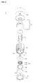
- Fig. 1 is a bottom perspective view of a lighting device 1 according to an embodiment of the present invention.
- Fig.2 is a top perspective view of the lighting device 1 of Fig. 1 .
- Fig. 3 is an exploded perspective view of the lighting device 1 of Fig. 1 .
- Fig. 4 is a longitudinal cross sectional view of the lighting device 1 of Fig. 1 .
- the lighting device 1 includes a guide member 100, a lens 110, a sealing ring 120, a light source 130, a heat radiating plate 140, a heat radiating body 150, a power supply controller 160, an inner case 170 and an outer case 180.
- Fig. 5 is a bottom perspective view of a heat radiating body 150 of the lighting device of Fig. 1 .
- Fig. 6 is a top perspective view of a heat radiating body 150.
- Fig. 7 is a cross sectional view taken along a line A-A' of Fig. 5 .
- the heat radiating body 150 includes a base 156 having a through hole 153, a cylindrical body 157 extending perpendicular to the base 156 and a heat radiating fin 158 formed on the outer peripheral surface of the body 157.
- the heat radiating body 150 receives the light source 130 and the power supply controller 160 and radiates heat generated from the light source 130 and/or the power supply controller 160.
- a first receiving groove 151 on which the power supply controller is disposed is formed on the upper surface of the heat radiating body 150.
- a second receiving groove 152 on which the light source 130 is disposed is formed on the lower surface of the heat radiating body 150.
- the first receiving groove 151 is absolutely required for receiving and disposing the power supply controller 160
- the second receiving groove 152 is not necessarily formed as shown in Fig. 13 .
- the light source 130 is disposed contacting with or close to the lower surface of the heat radiating body 150.
- the width and depth of the receiving grooves 151 and 152 are changeable depending on the width and thickness of the power supply controller 160 and the light source 130.
- At least one heat radiating fin 158 is disposed separately from each other at a predetermined interval on the outer peripheral surface of the body 157.
- Each heat radiating fin 158 has its predetermined width as viewed from the top or bottom of the heat radiating body 150.
- the heat radiating fin 158 has a board shape as viewed from the side of the heat radiating body 150 and is formed in the direction of length of the body 157.
- the heat radiating fin 158 as viewed from the top or bottom of the heat radiating body 150 looks like a saw-tooth shape or seems to have an uneven structure formed having a regular interval along the outer peripheral surface of the body 157 of the heat radiating body 150. More preferably, as the heat radiating body 150 is shown in Figs.
- the heat radiating fin 158 may have a shape of a circular arc bent perpendicular to the longitudinal direction of the heat radiating body 150 so as to increase the heat radiation efficiency by increasing a contact area with the air. Also preferably, heat radiating fin 158 can have a shape of a sine curve along the direction perpendicular to the longitudinal direction of the heat radiating body 150 (not shown). Such a heat radiating fin 158 causes the surface area of the heat radiating body 150 to be increased, improving the heat radiation efficiency.
- the number of the heat radiating fin 158 is increased, the contact area with the air is increased. Therefore, the heat radiation efficiency is improved. On the contrary, manufacturing cost is higher and structural vulnerability is generated. Since a heating value is variable according to a power capacity of the lighting device, it is necessary to determine an appropriate number of the heat radiating fin 158.
- the heat radiating body 150 of which the body 157 has a circular section as viewed from the top will be described. Referring to Figs. 8 and 10 , it is assumed that a line extending from an outermost end to a center of the body 157 is denoted by l, a line extending from an adjacent heat radiating fin 158 to the center of the body 157 is denoted by 'l", an acute angle between l and l' is denoted by ⁇ , and an outer diameter of the body 157 is denoted by ⁇ .
- the number of the heat radiating fins 158 is 18, an interval between the heat radiating fins 158 is 3.59 mm and a thickness of a part of each heat radiating fin 158 contacting with the body 157 is 3.59 mm, and when a lighting device consuming an electric power of 5W or 8W has a case where ⁇ is 17.14285 ⁇ is 55.00 mm, the number of the heat radiating fins 158 is 21, an interval between the heat radiating fins 158 is 2.77 mm and a thickness of a part of each heat radiating fin 158 contacting with the body 157 is 3.77 mm, and when a lighting device consuming an electric power of 15W has a case where ⁇ is 11.235 ⁇ is 77.00 mm, the number of the heat radiating fins 158 is 32, an interval between the heat radiating fins 158 is 3.65 mm and a thickness of a part of each heat
- the heat radiating body 150 is made of a metallic material or a resin material which has excellent heat radiation efficiency.
- the heat radiating body 150 is made of Fe, Al, Ni, Cu, Ag, Sn and Mg, etc., and is also made of an alloy including at least one of Fe, Al, Ni, Cu, Ag, Sn and Mg, etc. Carbon steel and stainless steel can be also adopted.
- An anti-corrosion coating or an insulation coating may be performed on the surface of the heat radiating body 150 within a range without affecting a thermal conductivity.
- the through hole 153 is formed on the bottom surface of the heat radiating body 150.
- the light source 130 is electrically connected to the power supply controller 160 by a second wiring 165 penetrating the through hole 153.
- a protection ring 155 is added to the through hole 153.
- the protection ring 155 prevents moisture and impurities from penetrating between the light source 130 and the heat radiating body 150, prevents an electrical short-circuit, EMI, EMS and so on caused by contacting the second wiring 165 with heat radiating body 150 and improves a withstand voltage characteristic.
- the protection ring 155 is made of a rubber material, a resin material, a silicon material or other electrical insulating material.
- a fastening member 154 is formed on the lateral surface of the lower part of the heat radiating body 150 such that the guide member 100 is securely coupled to the heat radiating body 150.
- the fastening member 154 has a hole for inserting a screw or a pinhole for a pin-coupling, thereby coupling strongly the guide member 100 to the heat radiating body 150 by using the screw or a pin.
- a first width D1 of the lower part of the heat radiating body 150 is less than a second width D2 of the other part of the heat radiating body 150.
- the first fastening member 154 is formed on the lower surface of the base 156 of the heat radiating body 150.
- Fig. 11 is a perspective view showing coupling of a light source 130 and a sealing ring of the lighting device of Fig. 1 .
- Fig. 12 is a cross sectional view taken along a line B-B' of Fig. 11 . It is assumed that a surface on which the light emitting device 131 is formed is an upper surface in Figs. 11 and 12 .
- the light source 130 includes a substrate 132 and at least one light emitting device 131 mounted on the substrate 132.
- the substrate 132 is made by printing a circuit pattern on an insulator.
- a common printed circuit board (PCB), a metal core PCB, a flexible PCB and a ceramic PCB and the like can be used as the substrate 132.
- the substrate 132 is made of a material capable of efficiently reflecting light. White and silver colors, etc., capable of efficiently reflecting light is formed on the surface of the substrate 132.
- At least one light emitting device 131 is mounted on the substrate 132.
- Each of a plurality of the light emitting devices 131 includes at least one light emitting diode (hereinafter, referred to as LED).
- the LEDs include various colors such as red, green, blue and white, each of which emits red, green, blue and white lights respectively.
- the light emitting device 131 is not necessarily mounted on an area of the upper surface of the substrate 132, and the area of the upper surface corresponds to the area to which the second wiring 165 is attached.
- the light emitting device 131 is not mounted on the center of the upper surface of the substrate 132, and the center of the upper surface corresponds to the center to which the second wiring 165 is attached.
- the light emitting device 131 is mounted on an area other than the center.
- the light source 130 is disposed in the receiving groove 152 of the heat radiating body 150. If the receiving groove 152 is not formed in the heat radiating body 150, the light source 130 is fixed strongly to the lower surface of the heat radiating body 150 by the guide member 100. A sealing ring 120 is coupled around the light source 130.
- the sealing ring 120 prevents moisture and impurities from penetrating between the guide member 100 and the light source 130 and causes the outer lateral surface of the light source 130 and the second receiving groove 152 of the heat radiating body 150 to be spaced from each other so that light source 130 cannot directly contact with the heat radiating body 150. As a result, an electrical short-circuit, EMI, EMS and so on of the lighting device 1 are prevented and a withstand voltage characteristic is enhanced.
- the sealing ring 120 is made of a rubber material, a resin material, a silicon material or other electrical insulating material and is coupled around the light source 130. Specifically, as shown in Fig. 12 , a diameter difference 121 is generated in the inner lower part of the sealing ring 120. The lateral surface and the circumference of the upper surface of the light source 130 are in contact with the sealing ring 120 having the diameter difference 121. A slope 122 is formed in the inner upper part of the sealing ring 120 such that light distribution of the light source 130 is improved.
- the sealing ring 120 strongly fixes and protects the light source 130, improving the reliability of the lighting device 1.
- the sealing ring 120 allows the lens 110 to be disposed apart from the light source 130 by a first distance "h". As a result, it is much easier to adjust the light distribution of the lighting device 1.
- a heat radiating plate 140 is attached to an opposite surface to the surface on which the light emitting device 131 of the light source 130 is disposed.
- the heat radiating plate 140 is attached to the receiving groove 152 as shown in Fig. 7 . If the receiving groove 152 is not formed in the heat radiating body 150, the heat radiating plate 140 is disposed close to the lower surface of the heat radiating body 150.
- the light source 130 is integrally formed with the heat radiating plate 140.
- the heat radiating plate 140 is made of a material having a high thermal conductivity such as a thermal conduction silicon pad or a thermal conduction tape and the like.
- the heat radiating plate 140 functions basically to transfer heat generated from the light source 130 to the heat radiating body 150.
- the heat radiating plate 140 is made of an insulating material, thereby preventing an electrical short-circuit, EMI, EMS and so on caused by contacting the light source 130 with heat radiating body 150 and improving a withstand voltage characteristic.
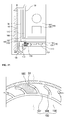
- Fig. 16 is a perspective view of a guide member 100 of the lighting device of Fig. 1 .
- Fig. 17 is a bottom view of the guide member 100 of Fig. 16 .
- the guide member 100 includes a base 108 having an opening 101 for allowing light radiated from the light source 130 to be seen through the lower part of the lighting device 1, a cover 109 extending perpendicular to the base 108, at least one first heat radiating hole 102 in either the base 108 or the cover 109, and a locking groove 103 for coupling the guide member 100 to the heat radiating body 150.
- the guide member 100 is shown in the form of a circular ring, the guide member 100 can have also shapes such as a polygon and an elliptical ring.
- At least the heat radiating hole 102 performs a function as an air inlet for allowing the air to flow to the inside of the lighting device 1.
- external air flows into a space partitioned between the outer case 180 and the outermost end of the heat radiating body 150 along the broken-lined arrow, and then flows to the outside of the lighting device 1.
- the air flow structure of the guide member 100 is not limited to this and can be changed variously.
- at least one of inner and outer covers 109 has at least one heat radiating groove 105 so that the air flows through the heat radiating groove 105.
- the guide member 100 when a transparent guide member 100 allows light radiated from the light source 130 to transmit the base 108 of the guide member 100, the guide member 100 does not have to include the opening 101.
- the guide member 100 presses the circumference of the light source 130 to the second receiving groove 152 of the heat radiating body 150, and, as shown in Fig. 39 , fixes the light source 130 by surrounding the outside of the circumference of the lower part of the heat radiating fin 158. Otherwise, the guide member 100 fixes the light source 130 to the base 156 of the heat radiating body 150 as shown in Fig. 14 .
- the guide member 100 fixes the light source 130 by pressing the light source 130 to the base 156 of the heat radiating body 150 and, as shown in Fig. 40 , surrounding the outside of the circumference of the lower part of the heat radiating fin 158. Otherwise, the guide member 100 fixes the light source 130 to the base 156 of the heat radiating body 150 as shown in Fig. 13 .
- At least one of the lens 110 and the sealing ring 120 is included between the guide member 100 and the light source 130.
- the transparent guide member 100 has a base 108 functioning as the lens 110, so that the lens 110 is not necessary.
- the sealing ring 120 is not necessarily included between the guide member 100 and the light source 130.
- the guide member 100 is made of an insulating material, without the sealing ring 120, only the guide member 100 is able to prevent the outer surface of the light source 130 from directly contacting with the heat radiating body 150. Accordingly, an electrical short-circuit, EMI, EMS and so on of the lighting device 1 are prevented and a withstand voltage characteristic is enhanced.
- the width of the opening 101 is required to be less than that of the light source 130.
- the base 108 can give an enough pressure to the lens 110, the sealing ring 120 and the circumference of the light source 130, and able to strongly fix the lens 110, the sealing ring 120 and the light source 130 to the heat radiating body 150. Therefore, the reliability of the lighting device 1 is improved.
- the guide member 100 can be coupled to the heat radiating body 150 through the locking groove 103.
- a hole of the first fastening member 154 of the heat radiating body 150 is in a line with the locking groove 103 of the guide member 100. Then, the guide member 100 is coupled to the heat radiating body 150 by inserting a screw or a pin into the locking groove 103 and the hole of the first fastening member 154.
- a screw thread is formed on both the outer peripheral surface of the second receiving groove 152 of the heat radiating body 150 and the inner peripheral surface of the cover 109 of the guide member 100. Therefore, the guide member 100 is coupled to the heat radiating body 150 without a pin or a screw.
- the lens 110 is disposed under the light source 130 and adjusts the distribution of light radiated from the light source 130.
- the lens 110 has various shapes.
- the lens 110 includes at least one of a parabola-shaped lens, a fresnel lens, a convex lens or a concave lens.
- the lens 110 is disposed under the light source 130 and spaced apart from the light source 130 by the first distance "h".
- the first distance "h" is greater than 0 mm and equal to or less than 50 mm in accordance with a design of the lighting device 1.
- the distance “h” is maintained by the sealing ring 120 disposed between the light source 130 and the lens 110. Otherwise, if another support for supporting the lens 110 is provided in the second receiving groove 152 of the heat radiating body 150, the distance “h” is maintained between the light source 130 and the lens 110 without using the sealing ring 120.
- the lens 110 is fixed by the guide member 110. Referring to Figs. 4 and 14 to 17 , the base 108 of the guide member 100 contacts with the lens 110. The lens 110 and the light source 130 are pressed and fixed to the second receiving groove 152 of the heat radiating body 150 by the base 108 of the guide member 100. If the second receiving groove is not formed in the heat radiating body 150, the base 108 of the guide member 100 presses and fixes the lens 110 and the light source 130 to the base 156 of the heat radiating body 150.
- the lens 110 is made of glass, polymethylmethacrylate (PMMA) and polycarbornate (PC) and so on. According to a design of the lighting device 1, the lens 110 includes fluorescent substance. A photo luminescent film (PLF) including the fluorescent substance is attached to a light emitting surface or a light emitting surface of the lens 110. Light radiated from the light source 130 by the fluorescent substance is emitted with a varied wavelength.
- PMMA polymethylmethacrylate
- PC polycarbornate
- the base 108 of the transparent guide member 100 functions as the lens 110.
- a description of the lens 110 is applied to the base 108 of the guide member 100 in the same manner.
- Fig. 27 is a perspective view of an inner case of the lighting device 1 of Fig. 1 .
- an inner case 170 includes a terminal 175, a cylindrical inner body 174 extending from a side of the terminal 175 and inserted into the inside of the heat radiating body 150, and a first guide 172 formed perpendicular to the outer peripheral surface of the cylindrical inner body 174 adjacent to the terminal.
- the inner case 170 is made of a material with excellent insulating properties and endurance, for example, a resin material.
- the inner body 174 occupies a lower part of the inner case 170.
- the inner body 174 is inserted into the first receiving groove 151 of the heat radiating body 150 and is disposed between the power supply controller 160 and the heat radiating body 150, thereby preventing the power supply controller 160 from contacting with the heat radiating body 150.
- an electrical short-circuit, EMI, EMS and so on are prevented and a withstand voltage characteristic of the lighting device 1 is enhanced.
- the terminal 175 occupies an upper part of the inner case 170.
- the terminal 175 is connected to an external power supply in the form of a socket. That is, the terminal 175 includes a first electrode 177 at the top thereof, a second electrode 178 on the lateral surface thereof and an insulating member 179 between the first electrode 177 and the second electrode 178.
- the first and second electrodes 177 and 178 are provided with electric power by an external power supply.
- the shape of the terminal 175 is variously changed based on a design of the lighting device 1.
- the first guide member 172 is formed on the interface between the inner body 174 and the terminal 175, so that the first guide member 172 has a longer diameter than that of the first receiving groove 151. As a result, the first receiving groove 151 is able to receive only the inner body 174 of the inner case 170.
- the first guide member 172 includes at least one first coupling hole 173.
- the inner case 170 is coupled to an outer case 180 by inserting a screw or a pin into at least one first coupling hole 173.
- a plurality of second heat radiating holes 176 are formed in the inner case 170, improving the heat radiation efficiency of the inside of the inner case 170.
- the power supply controller 160 is disposed in the first receiving groove 151 of the heat radiating body 150 and is electrically connected to the light source 130 by the second wiring 165 penetrating the through hole 153 formed in the base 156 of the heat radiating body 150.
- the power supply controller 160 is operated by electric power being fed.
- the power supply controller 160 includes a supporting substrate 161 and a plurality of parts 162 mounted on the supporting substrate 161.
- a plurality of the parts 162 include, for example, a DC-DC converter converting an alternating current supplied from an external power supply into an direct current, a driving chip controlling to drive the light source 130, an electrostatic discharge (ESD) protective device protecting the light source 130.
- ESD electrostatic discharge
- the power supply controller 160 is electrically connected to the light source 130 and the terminal 175 of the inner case 170 by the second wiring 165 and a first wiring 164 respectively.
- the first wiring 164 is connected to the first electrode 177 and the second electrode 178 of the terminal 175 and is supplied with electric power by an external power supply.
- a power connection terminal (not shown), which is connected directly to the first and the second electrodes 177 and 178, can be formed on the supporting substrate 161 without the first wiring 164.
- the second wiring 165 passes through the through hole 153 of the heat radiating body 150 and connects electrically the power supply controller 160 to the light source 130.
- the light source 130 is formed in the form of an integral module consisting of the light emitting device 131, the substrate 132 and the power supply controller 160.
- the power supply controller 160 is formed in the lower part of the heat radiating body 150.
- the supporting substrate 161 is disposed horizontally within the inner body 174 of the inner case 170, it is possible to start and operate the light source 130 of the power supply controller 160.
- the air flows in up and down direction in the inner case 170 due to convection current, thereby improving the heat radiation efficiency of the lighting device 1 and particularly helping the heat radiation efficiency of the power supply controller 160 to be enhanced, as compared with a case where the supporting substrate 161 is disposed horizontally.
- the supporting substrate 161 is not necessarily disposed in the vertical direction in the inner case 170, as long as the air is able to flow in the inner body 174 in the up and down direction of the heat radiating body 150, it is possible to obtain the same effect as that of a case where the supporting substrate 161 is disposed in the vertical direction. Therefore, it does not matter that the supporting substrate 161 is sloping slightly with respect to the vertical direction.
- the supporting substrate 161 does not prevent the air from flowing upward in the inner body 174, it is also possible to increase the heat radiation efficiency of the power supply controller 160.
- the supporting substrate 161 even though the supporting substrate 161 is disposed in a horizontal direction to the base 156 of the heat radiating body 150, the supporting substrate 161 having a through hole formed therein causes the air to pass through supporting substrate 161 and flow upward and downward in the inner body 174. Otherwise, when the supporting substrate 161 disposed horizontally has a different shape from the horizontal section shape of the inner body 174 or when the supporting substrate 161 having the same shape as the horizontal section shape of the inner body 174 has a less diameter than the inner diameter of the inner body 174, the air is able to flow upward and downward in the inner body 174. Eventually, the inside of the inner body 174 is not shielded upward and downward, the air is able to flow in the inner body 174, thereby improving the heat radiation efficiency of the lighting device 1 and particularly helping the heat radiation efficiency of the power supply controller 160.
- the weight of the power supply controller 160 during a long-term use of the lighting device 1 causes the power supply controller 160 to move downward, so that the second wiring 165 is pressed and damaged by the supporting substrate 161.
- the second wiring 165 is pressed by the supporting substrate 161 and is damaged by being put between the supporting substrate 161 and the base 156 of the heat radiating body 150 during the process of assembling the lighting device 1.
- a supporter 159 is formed around the through hole 153 in the base 156 of the heat radiating body 150, the supporter 159 supports the supporting substrate 161 and prevents the second wiring 165 from being damaged.
- the supporter 159 surrounds the through hole 153 and is formed on the base in the form of a protruding cylindrical shape.
- the supporter 159 is formed in the form of a bar lying on the base 156.
- the supporter 159 can have any shape capable of spacing the supporting substrate 161 and the base 156 of the heat radiating body 150.
- the supporter 159 is disposed apart from the through hole 153 by a predetermined distance, which produces the same effect as that of the embodiment of Fig. 30 .
- a groove for coupling the power supply controller 160 when a groove for coupling the power supply controller 160 is formed in the supporter 159, the supporting substrate 161 is inserted into the groove, preventing the power supply controller 160 from moving within the receiving groove 151 and fixing the supporting substrate 161.
- a sealing member made of a rubber material or a resin material can be placed between the supporting substrate 161 and the groove for coupling the power supply controller 160.
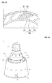
- Figs. 34 to 38 are perspective views of an outer case 180 as viewed from the top.
- the outer case 180 is coupled to the inner case 170, receives the heat radiating body 150, the light source 130 and the power supply controller 160, etc., and forms an external shape of the lighting device 1.
- the outer case 180 is made of a material having an excellent insulation and endurance such as a resin material.
- the outer case 180 can have a polygon section or elliptical section and so on. Since the outer case 180 surrounds the heat radiating body 150, it is possible to prevent a burn accident due to the heat generated from the operation of the lighting device 1 and an electric shock during a repair or exchange of the lighting device 1.
- the outer case 180 includes an outer wall 181 which is spaced apart from the heat radiating body 150 by a predetermined interval and surrounds the heat radiating body 150, a ring-shaped second guide 187 contacting directly with the first guide 172, and at least one projection 188 connecting the outer wall 181 with the second guide 187.
- the outer case 180 is spaced apart from the heat radiating body 150 by a predetermined interval and surrounds the heat radiating body 150.
- the outer case 180 is spaced apart from a prominence (a) denoted by a dotted-line among the prominence (a) and depression (b) of the heat radiating body 150 and surrounds the heat radiating body 150.
- the outer case 180 includes at least one ventilating hole 182, i.e., a space between the outer wall 181 and the second guide 187 such that the air is able to flow to the inside and outside of the lighting device 1, thereby allowing the air to flow smoothly in the lighting device 1 and improving the heat radiation efficiency of the lighting device 1.
- At least one ventilation hole 182 is formed in the edge of the upper surface of the outer case 180.
- the outermost edge portion and innermost edge portion have circular arc shapes, including a circular shape, an elliptical shape and a polygon shape and the like.
- the ventilation hole 182 can be formed on the outer wall 181 (not shown).
- a second coupling groove 183 for coupling the outer case 180 and inner case 170 is formed on the second guide 187 or on at least one projection 188.
- the second guide 187 is not provided to the outer case 180.
- the outer case 180 includes at least one projection 188 includes both the outer wall 181 surrounding the heat radiating body 150 and at least one projection 188 connecting the outer wall 181 with the first guide 172.
- the projection 188 includes the second coupling groove 183 for coupling the first guide 172 shown in Fig. 27 to the outer case 180.
- the outer case 180 is spaced apart from the heat radiating body 150 by a predetermined distance and surrounds the heat radiating body 150.
- the outer case 180 is spaced apart from a prominence (a) denoted by a dotted-line among the prominence (a) and depression (b) of the heat radiating body 150 and surrounds the heat radiating body 150.
- the inner case 170 is covered with the outer case 180 in the direction from the terminal 175 to the lower part of the inner case 170.
- the second guide 187 is placed between the first guide 172 and at least one projection 188. Accordingly, the outer case 180 and the inner case 170 are coupled to each other by inserting a screw or a pin into the second coupling groove 183.
- the inner body 174 of the inner case 170 passes through an opening of the outer case 180 in the direction from the top of the outer case 180 to the lower part of the outer case 180 and contacts with the outer case 180. Subsequently, the first coupling groove 173 comes in a line with the second coupling groove 183. Thus, the outer case 180 and the inner case 170 are coupled to each other by inserting a screw or a pin into the first coupling groove 173.
- a screw hole or a pin hole is formed on the upper surface of the body 157 of the heat radiating body 150.
- the first coupling groove 173, the second coupling groove 183 and the screw hole or the pin hole come in a line with each other.
- the outer case 180, the inner case 170 and the heat radiating body 150 are coupled to each other by inserting a screw or a pin into the hole and the grooves.
- the outer case 180, the inner case 170 and the heat radiating body 150 it is not necessary to couple the outer case 180, the inner case 170 and the heat radiating body 150 at a time.
- the inner case 170 and the outer case 180 can be coupled to each other by using another screw or pin.
- the outer case 180 and the heat radiating body 150 are first coupled to each other by using a screw or a pin, the outer case 180 and the inner case 170 can be coupled to each other by using another screw or pin.
- a screw or a pin inserted into the first coupling groove 173, the second coupling groove 183 and the screw hole or the pin hole formed on the upper surface of the body 157 of the heat radiating body 150 is a separate member. It is acceptable to use a pin formed integrally with the upper surface of the body 157 of the heat radiating body 157, a pin formed integrally with the first guide 172, and a pin formed integrally with the second guide 187. In this case, the heat radiating body 157, the inner case 170 and the outer case 180 are coupled to each other by using an interference fit.
- an upward screw is integrally formed with the upper surface of the body 157 of the heat radiating body 150, and the first coupling groove 173 and the second coupling groove 183 come in a line with the screw.
- an LED lighting device includes the outer case 180
- its heat radiation efficiency may generally decrease.
- the heat radiating body 150, the inner case 170 and the outer case 180 are coupled to each other, the heat radiation efficiency is sufficiently increased through a chimney effect and a contact area between the heat radiating body 150 and the outer case 180 is minimized.
- a principle of obtaining an excellent heat radiating effect through a chimney effect will be described below in detail in another part of this application.
- the lighting device 1 is easy to handle.
- its heat radiation efficiency should be reduced in order to easily handle the existing lighting device.
- the existing lighting device is hard to handle in order to obtain the high heat radiation efficiency. Accordingly, in the embodiments shown in Figs. 13 to15, there is a difference between the existing lighting devices and the lighting device 1 of the present invention in that the lighting device 1 obtains the high heat radiation efficiency and is easy to handle.
- the lateral surface of the outer case 180 may include at least a marking groove 185 and a hole 184.
- the marking groove 185 is used for easily handling the lighting device 1.
- the hole 184 is used for increasing the heat radiation efficiency.
- the hole 184 and the marking groove 185 may have various shapes including the shapes shown in the embodiment.
- the heat radiation efficiency shown in the foregoing embodiments is much more excellent than that of an existing LED lighting device.
- the chimney effect means that smoke or air flows in the vertical space of a building due to a density difference, i.e., buoyancy caused by a temperature difference between the inside of a building and external air.
- the chimney effect is generally used in the field of building construction.
- the principle of the lighting device 1 of the present invention will be described with reference to Figs. 3 , 13 to 15 and 39 to 42 .
- heat from the light source 130 is directly transferred to the heat radiating body 150 or transferred to the heat radiating body 150 through the heat radiating plate 140 interposed between the heat radiating body 150 and the light source 130.
- the heat is transferred from the heat radiating body 150 to the air in a space formed between the heat radiating body 150 and the outer case 180, so that the air is heated. Since the heated air has a lower density than that of the external air, the air rises upward due to buoyancy.
- the rising air which is denoted by S2 in Fig. 42 , is divided by the upper part of the outer case 180 and the outer lateral surface of the upper part of the body 157 of the heat radiating body 150, and then the air passes through an open space connected fluidly to the external air and goes out.
- the heat radiating hole 102 if the heat radiating hole 102 is formed in the guide member 100, the heat radiating hole 102 performs a function of a passage allowing the external air to flow to the inside of the lighting device. Even if the heat radiating hole 102 is not formed in the guide member 100, like the embodiment shown in Figs. 13 to 15 , a passage is formed, which allows the air to flow in between the upper part of the outer case 180 and the lower part of the outer peripheral surface of the body 157.
- the heat radiating fin 158 is spaced apart from the outer case 180, and thereby even reducing heat transferred from the heat radiating body 150 to the outer case 180.
- Figs. 43 to 45 show that the width of the outer case 180 of the lighting device 1 is more decreased toward a further upper part of the outer case 180.
- the section of the heat radiating body 150 has a trapezoidal shape in such a manner as to be parallel with the outer case 180.
- the end of lateral surface of the heat radiating fin 158 is parallel with the outer case 180.
- the air passes through the parts of S1 and S2 in order of S1 to S2, so that the air flows more smoothly. Accordingly, the heat radiation efficiency is more improved.
- Equation (1) P represents a pressure; ⁇ represents a density; u represents a speed; g represents an acceleration of gravity; and h represents a height.
- a subscript 1 represents a bottom; and a subscript 2 represents a top.
- A represents a cross section area; and u represents a speed.
- a subscript 1 represents a bottom; and a subscript 2 represents a top.
- Equation (1) can be rearranged by the following equation (3).
- P 1 - P 2 1 2 ⁇ ⁇ ⁇ ⁇ 2 2 - ⁇ 1 2 + ⁇ g h 2 - h 1
- a cross sectional area generated by cutting a space determined by both the outer case 180 and the lower part of the heat radiating body 150 in the direction perpendicular to the longitudinal direction of the heat radiating body 150 is denoted by S1 and a cross sectional area generated by cutting a space determined by the outer case 180 and the upper part of the heat radiating body 150 in the direction perpendicular to the longitudinal direction of the heat radiating body 150 is denoted by S2, a pressure of an air inlet port having a cross sectional area of S1 is greater than that a pressure of an air outlet port having a cross sectional area of S2. Therefore, when air flows due to the chimney effect, the air is forced to flow more smoothly.
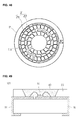
- Fig. 47 is a cross sectional view of a substrate of the heat radiating body.
- the substrate 132 includes a first conductive layer L1, a first insulation layer P1, a FR4 copper-clad laminate sheet C, a second insulation layer P2 and a second conductive layer L2.
- the substrate 132 may further include a third conductive layer L3 and a fourth conductive layer L4.
- the third conductive layer L3 is formed between the first insulation layer P1 and the FR4 copper-clad laminate sheet C.
- the fourth conductive layer L4 is formed between the FR4 copper-clad laminate sheet C and the second insulation layer P2. That is, the third conductive layer L3 and the fourth conductive layer L4 may be omitted.
- the plurality of the light emitting devices 131 are arranged on the first conductive layer L1 in the form of a circle.
- the first insulation layer P1 is disposed under the first conductive layer L1.
- a distance from the central axis of the substrate 132 to the outermost end of the first conductive layer L1 is less than a distance from central axis of the substrate 132 to the outermost end of the first insulation layer P1 by a predetermined distance "D".
- the central axis penetrates the center of the circular substrate 132.
- the substrate 132 may have a polygonal shape such as a triangle or a quadrangle and the like as well as a circle shown in Fig. 9 . Therefore, in this specification, there is no requirement that the central axis penetrates the center of the circular substrate 132.
- the first conductive layer L1 becomes further from the inner peripheral surface formed by the second receiving groove 152 of the heat radiating body 150, so that it is possible to prevent electric shock between the heat radiating body 150 and the substrate 132. As a result, a withstand voltage of the lighting device 1 can be improved.
- the first conductive layer L1 is made of a material having high thermal conductivity and high electrical conductivity, for example, copper, etc.
- the first insulation layer P1 is disposed between the first conductive layer L1 and the third conductive layer L3.
- a via H is formed in the first insulation layer P1 so as to electrically connect the first conductive layer L1 with the third conductive layer L3. It is desirable that the via H is made of a material having high thermal conductivity and high electrical conductivity, for example, copper.
- the first insulation layer P1 is required to be formed of prepreg.
- the FR4 copper-clad laminate sheet C is disposed between the third conductive layer L3 and the fourth conductive layer L4.
- a via H is formed in the FR4 copper-clad laminate sheet C so as to electrically connect the third conductive layer L3 with the fourth conductive layer L4.
- the second insulation layer P2 is disposed between the fourth conductive layer L4 and the second conductive layer L2.
- a via H is formed in the second insulation layer P2 so as to electrically connect the fourth conductive layer L4 with the second conductive layer L2. It is desirable that the via H is made of a conductor like copper.
- the second insulation layer P2 is required to be formed of prepreg.
- the second conductive layer L2 is disposed under the second insulation layer P2.
- a distance from the central axis of the substrate 132 to the outermost end of the second conductive layer L2 is less than a distance from the central axis of the substrate 132 to the outermost end of the second insulation layer P2 by a predetermined distance "D".
- the central axis penetrates the center of the circular substrate 132.
- the substrate 132 may have a polygonal shape such as a triangle or a quadrangle and the like as well as a circle shown in Fig. 9 .
- the second conductive layer L2 becomes further from the inner peripheral surface formed by the second receiving groove 152 of the heat radiating body 150, so that it is possible to prevent electric shock between the heat radiating body 150 and the substrate 132. As a result, a withstand voltage of the lighting device 1 can be improved.
- a solder mask S is formed on both the first conductive layer L1 except areas on which the plurality of the light emitting devices 131 are disposed and the first insulation layer P1 except areas on which the first conductive layer L1 is disposed.
- solder mask S is formed on the second insulation layer P2 except areas on which the second conductive layer L2 is disposed.
- the solder mask S is required to have a white based color in order to easily reflect light emitted from the plurality of the light emitting devices 131.
- Fig. 48 is a view for describing the shape of the first conductive layer L1 shown in Fig. 47 .
- the first conductive layer L1 is divided in advance into zones Z on which a plurality of the light emitting devices 131 are disposed respectively.
- the zones Z on which the plurality of the light emitting devices 131 are to be disposed are composed of a first rectangular zone Z1 and a second lozenge-shaped zone Z2. In the zones Z1 and X2, it is the zone Z2 that the plurality of the light emitting devices 131 are disposed on.
- a distance from the central axis of the substrate 132 to the outermost end of the first conductive layer L1 is less than a distance from the central axis of the substrate 132 to the outermost end of the first insulation layer P1 by a predetermined distance "D".
- the predetermined distance "D" is required to be at least 5 mm.
- Table 1 shows withstand voltage characteristic experimental data according to the predetermined distance "D".
- Table 1 D withstand voltage characteristic result 1 mm FAIL at 2.0 KV 5 mm PASS at 4.0 KV
- the lighting device 1 of the present invention has a power of 15 watts (W)
- the light emitting module substrate 132 has a size of 69 ⁇
- the pad of the heat radiating body 150 has a size of 70 ⁇
- the pad of the heat radiating body 150 has a thickness of 0.4 mm
- the through hole 153 has a size of 15 ⁇
- only the predetermined distance "D" is changed.
- high voltage the maximum voltage is 4.0 KV
- high current the maximum current is 100 mA
- the experimental results are as follows. When the predetermined distance "D" is 1 mm, the heat radiating body 150 is electrically short-circuited at 2.0 KV with the light emitting module substrate 132 so that the withstand voltage characteristic is not satisfied (FAIL). However, when the predetermined distance "D” is 5 mm, it can be discovered that the heat radiating body 150 is not electrically short-circuited at 4.0 KV with the light emitting module substrate 132 (PASS).
- the first conductive layer L1 and the second conductive layer L2 are required to be spaced apart by a distance of at least 5 mm from the outermost ends of the first insulation layer P1 and the second insulation layer P2.
- Fig. 49 is a cross sectional side view of the light emitting device 131 mounted on the lighting device 1 according to the embodiment.
- the light emitting device 131 includes a body 20, a first electrode layer 31 and a second electrode layer 32 which are disposed on the body 20, and a light emitting chip 10 which is disposed on one of the body 20, the first electrode layer 31 and the second electrode layer 32 and is electrically connected to the first electrode layer 31 and the second electrode layer 32 and emits light.
- the body 20 is formed of at least one of a resin material like polyphthalamide (PPA), Si, a metallic material, photo sensitive glass (PSG), Al2O3 and PCB.
- a resin material like polyphthalamide (PPA), Si, a metallic material, photo sensitive glass (PSG), Al2O3 and PCB.
- the top surface of the body 20 may have various shapes such as a quadrangle, a polygon and a circle and the like according to the use and design of the light emitting device 131.
- a cavity may be formed to open the upper part of the body 20.
- the cavity may have a shape of a cup and a concave vessel and the like.
- the inner surface of the cavity may be vertical to the ground or inclined.
- the shape of the cavity as viewed from the top may be a circle, a quadrangle, a polygon and an ellipse and the like.
- the first electrode layer 31 and the second electrode layer 32 are electrically separated from each other and disposed on the body 20.
- the first electrode layer 31 and the second electrode layer 32 are electrically connected to the light emitting chip 10 so that electric power can be supplied to the light emitting chip 10.
- the first electrode layer 31 and the second electrode layer 32 may include a metallic material, for example, at least one of Ti, Cu, Ni, Au, Cr, Ta, Pt, Sn, Ag and P.
- the first electrode layer 31 and the second electrode layer 32 may also have a single layer structure or a multi layer structure. There is no limit to the structures of the first electrode layer 31 and the second electrode layer 32.
- One ends of the first electrode layer 31 and the second electrode layer 32 are disposed inside the cavity of the body 20.
- the other ends of the first electrode layer 31 and the second electrode layer 32 are disposed to be exposed outside the body 20.
- the light emitting chip 10 may be disposed on one of the body 20, the first electrode layer 31 and the second electrode layer 32.
- the light emitting chip 10 is electrically connected to the first electrode layer 31 and the second electrode layer 32 and is supplied with electric power so that it can emit light. Heat generated from the light emitting chip 10 is transferred to the first electrode layer 31 and the second electrode layer 32 and is radiated to the outside.
- the light emitting chip 10 may include at least one light emitting diode (LED).
- the LED may include a color LED emitting red, green, blue and white light, etc., or ultra violet (UV) LED emitting ultraviolet light. There is no limit to the kind of the LED.
- the light emitting chip 10 is, as shown, electrically connected to the first electrode layer 31 and the second electrode layer 32 in a wire bonding manner or in a flip-chip manner and in a die-bonding process and the like.
- a seal material 40 may be formed inside the cavity in order to seal and protect the light emitting chip 10.
- the seal material 40 may include a fluorescent material.
- the seal material 40 may be formed of a silicon material or a resin material.
- the seal material 40 is formed by filling the cavity with the silicon material or the resin material and curing them. However, there is no limit to a method for forming the seal material 40.
- the fluorescent material can be added to the seal material 40.
- the fluorescent material is excited by a first light emitted from the light emitting chip 10 and generates a second light.
- the light emitting chip 10 is a blue LED and the fluorescent material is a yellow fluorescent material
- the yellow fluorescent material is excited by blue light and emits yellow light.
- the blue light is mixed with the yellow light, the light emitting device 131 can provide white light.
- the invention ralates to the following items:
Abstract
a heat radiating body which comprises a base and a cylindrical body extending to the base;
a light source disposed on a part of the heat radiating body; and
an outer case being spaced apart from an outer surface of the heat radiating body and surrounding the heat radiating body.
Description
- This embodiment relates to a lighting device.
- A light emitting diode (hereinafter, referred to as LED) is a semiconductor element for converting electric energy into light. An electric bulb has a short life span. A longer time for use of the electric bulb causes the life span to be shorter. For this reason, the electric bulb is required to check and change cyclically. Therefore, there has been a problem of paying for the additional cost of changing and managing the electric bulb. As compared with existing light sources such as a fluorescent lamp and an incandescent electric lamp and so on, the LED has advantages of low power consumption, a semi-permanent span of life, a rapid response speed, safety and an environment-friendliness. Therefore, many researches are devoted to substitution of the existing light sources with the LED. The LED is used as a light source for lighting devices, for example, various lamps used interiorly and exteriorly, a liquid crystal display device, an electric sign and a street lamp and the like, as a result, is now increasingly taking the place of the electric bulb. However, since the LED tends to be vulnerable to heat generated from its operation, most of LED lighting devices are employing various means for efficiently radiating heat. In the publication of Korean patent application No.
10-2009-0130473 10-2009-009831 - One embodiment is a lighting device. The lighting device includes:
- a heat radiating body which comprises a base and a cylindrical body extending to the base;
- a light source disposed on a part of the heat radiating body; and
- an outer case being spaced apart from an outer surface of the heat radiating body and surrounding the heat radiating body.
-
-
Fig. 1 is a bottom perspective view of a lighting device according to an embodiment of the present invention. -
Fig.2 is a top perspective view of the lighting device ofFig. 1 . -
Fig. 3 is an exploded perspective view of the lighting device ofFig. 1 . -
Fig. 4 is a longitudinal cross sectional view of the lighting device ofFig. 1 . -
Fig. 5 is a bottom perspective view of aheat radiating body 150 of the lighting device ofFig. 1 . -
Fig. 6 is a top perspective view of aheat radiating body 150 of the lighting device ofFig. 1 . -
Fig. 7 is a cross sectional view taken along a line A-A' ofFig. 5 . -
Fig. 8 is a plan view of a heat radiating body used in a lighting device consuming an electric power of 3.5W. -
Fig. 9 is a plan view of a heat radiating body used in a lighting device consuming an electric power of 5W or 8W. -
Fig. 10 is a plan view of a heat radiating body used in a lighting device consuming an electric power of 15W -
Fig. 11 is a perspective view showing coupling of alight source 130 and a sealing ring of the lighting device ofFig. 1 . -
Fig. 12 is a cross sectional view taken along a line B-B' ofFig. 11 . -
Fig. 13 is a view showing a left side of a longitudinal section of a lighting device without a sealing ring. -
Fig. 14 is a view showing a left side of a longitudinal section of a lighting device having a fastening member formed on the lower surface of a base of a heat radiating body. -
Fig. 15 is a view showing a left side of a longitudinal section of a lighting device having a heat radiating body and a guide member which are coupled without a pin or a screw. -
Fig. 16 is a perspective view of aguide member 100 of the lighting device ofFig. 1 . -
Fig. 17 is a bottom view of theguide member 100 ofFig. 16 . -
Fig. 18 is a perspective view of aguide member 100A of the lighting device ofFig. 1 in accordance with another embodiment of the present invention. -
Fig. 19 is a perspective view of aguide member 100B of the lighting device ofFig. 1 in accordance with further another embodiment of the present invention. -
Fig. 20 is a view showing a modified embodiment of a transparent cover of theguide member 100 ofFig. 16 . -
Fig. 21 is a view showing another modified embodiment of a transparent cover of theguide member 100 ofFig. 16 . -
Fig. 22 is a view showing further another modified embodiment of a transparent cover of theguide member 100 ofFig. 16 . -
Fig. 23 is a view showing yet another modified embodiment of the transparent cover of theguide member 100 ofFig. 16 . -
Fig. 24 is a view showing a modified embodiment of theguide member 100 ofFig. 16 having abase 108 without a firstheat radiating hole 102. -
Fig. 25 is a view showing another modified embodiment of theguide member 100 ofFig. 16 having thebase 108 without the firstheat radiating hole 102. -
Fig. 26 is a view showing further another modified embodiment of theguide member 100 ofFig. 16 having thebase 108 without the firstheat radiating hole 102. -
Fig. 27 is a perspective view of an inner case of the lighting device ofFig. 1 . -
Fig. 28 is a longitudinal cross sectional view of a lower part of a lighting device having asupporter 159 formed on abase 156 of aheat radiating body 150 in accordance with an embodiment of the present invention. -
Fig. 29 is a longitudinal cross sectional view of a lower part of a lighting device having asupporter 159, which includes a groove for coupling apower supply controller 160, formed on abase 156 of aheat radiating body 150 in accordance with an embodiment of the present invention. -
Fig. 30 is a plan view of aheat radiating body 150 used in the lighting device shown inFig. 28 . -
Fig. 31 is a plan view of a modified embodiment of aheat radiating body 150 used in the lighting device shown inFig. 28 . -
Fig. 32 is a plan view of aheat radiating body 150 used in the lighting device shown inFig. 29 . -
Fig. 33 is a plan view of a modified embodiment of aheat radiating body 150 used in the lighting device shown inFig. 29 . -
Fig. 34 is a perspective view of anouter case 180 of the lighting device ofFig. 1 . -
Fig. 35 is a perspective view of a modified embodiment of anouter case 180 of the lighting device ofFig. 1 . -
Fig. 36 is a perspective view of another modified embodiment of anouter case 180 of the lighting device of -
Fig. 1 . -
Fig. 37 is a perspective view of further another modified embodiment of anouter case 180 of the lighting device ofFig. 1 . -
Fig. 38 is a perspective view of yet another modified embodiment of anouter case 180 of the lighting device ofFig. 1 . -
Fig. 39 is an enlarged cross sectional view showing an air flow into the inside of the lighting device ofFig.1 . -
Fig. 40 is an enlarged cross sectional view showing an air flow into the inside of a lighting device ofFig.1 in accordance with another embodiment of the present invention. -
Fig. 41 is a view showing an area of an air inlet of the lighting device ofFig. 1 as viewed from the bottom thereof. -
Fig. 42 is a top view showing an area of an air inlet of the lighting device ofFig. 1 as viewed from the top thereof. -
Fig. 43 is a perspective view of a lighting device to which chimney effect is applied. -
Fig. 44 is a front view of aheat radiating body 150 used in the lighting device in accordance with the embodiment ofFig. 43 . -
Fig. 45 is a longitudinal cross sectional view of theheat radiating body 150 ofFig. 44 . -
Fig. 46 is a view used for describing Bernoulli's theorem and a continuity equation of an incompressible flow. -
Fig. 47 is a cross sectional view of a substrate of the heat radiating body. -
Fig. 48 is a view for describing a shape of a first conductive layer. -
Fig. 49 is a cross sectional side view of a light emitting device mounted on the lighting device. - Hereinafter, an embodiment will be described in detail with reference to the accompanying drawings.
- It will be understood that when an element is referred to as being 'on' or "under" another element, it can be directly on/under the element, and one or more intervening elements may also be present.
- In describing embodiments, if there is no particular standard for the "top" or "bottom" of each layer, it is assumed that a side where a
light source 130 is disposed is the "top" and a side where a terminal 175 is disposed is the "bottom". However, inFigs. 11 and12 , a surface on which alight emitting device 131 is formed is assumed to be an upper surface. The thickness or size of each layer is exaggerated, omitted or schematically shown in the figures, for the convenience and clarity of description. Further, the size of each component does not necessarily represent its actual size. -
Fig. 1 is a bottom perspective view of alighting device 1 according to an embodiment of the present invention.Fig.2 is a top perspective view of thelighting device 1 ofFig. 1 .Fig. 3 is an exploded perspective view of thelighting device 1 ofFig. 1 .Fig. 4 is a longitudinal cross sectional view of thelighting device 1 ofFig. 1 . - Referring to
Figs. 1 to 4 , thelighting device 1 includes aguide member 100, alens 110, a sealingring 120, alight source 130, aheat radiating plate 140, aheat radiating body 150, apower supply controller 160, aninner case 170 and anouter case 180. - Hereinafter, each component of the
light device 1 according to an embodiment of the present invention will be described in detail. Moreover, a principle of obtaining an excellent heat radiation efficiency of thelight device 1 according to an embodiment of the present invention will be described as well. -
Fig. 5 is a bottom perspective view of aheat radiating body 150 of the lighting device ofFig. 1 .Fig. 6 is a top perspective view of aheat radiating body 150.Fig. 7 is a cross sectional view taken along a line A-A' ofFig. 5 . - Referring to
Figs. 4 to 7 , theheat radiating body 150 includes a base 156 having a throughhole 153, acylindrical body 157 extending perpendicular to thebase 156 and aheat radiating fin 158 formed on the outer peripheral surface of thebody 157. - The
heat radiating body 150 receives thelight source 130 and thepower supply controller 160 and radiates heat generated from thelight source 130 and/or thepower supply controller 160. Afirst receiving groove 151 on which the power supply controller is disposed is formed on the upper surface of theheat radiating body 150. Asecond receiving groove 152 on which thelight source 130 is disposed is formed on the lower surface of theheat radiating body 150. Here, while thefirst receiving groove 151 is absolutely required for receiving and disposing thepower supply controller 160, thesecond receiving groove 152 is not necessarily formed as shown inFig. 13 . In this case, thelight source 130 is disposed contacting with or close to the lower surface of theheat radiating body 150. The width and depth of the receivinggrooves power supply controller 160 and thelight source 130. - Referring to
Figs. 5 and6 , at least oneheat radiating fin 158 is disposed separately from each other at a predetermined interval on the outer peripheral surface of thebody 157. Eachheat radiating fin 158 has its predetermined width as viewed from the top or bottom of theheat radiating body 150. Theheat radiating fin 158 has a board shape as viewed from the side of theheat radiating body 150 and is formed in the direction of length of thebody 157. Theheat radiating fin 158 as viewed from the top or bottom of theheat radiating body 150 looks like a saw-tooth shape or seems to have an uneven structure formed having a regular interval along the outer peripheral surface of thebody 157 of theheat radiating body 150. More preferably, as theheat radiating body 150 is shown inFigs. 5 to 10 , theheat radiating fin 158 may have a shape of a circular arc bent perpendicular to the longitudinal direction of theheat radiating body 150 so as to increase the heat radiation efficiency by increasing a contact area with the air. Also preferably,heat radiating fin 158 can have a shape of a sine curve along the direction perpendicular to the longitudinal direction of the heat radiating body 150 (not shown). Such aheat radiating fin 158 causes the surface area of theheat radiating body 150 to be increased, improving the heat radiation efficiency. - If the number of the
heat radiating fin 158 is increased, the contact area with the air is increased. Therefore, the heat radiation efficiency is improved. On the contrary, manufacturing cost is higher and structural vulnerability is generated. Since a heating value is variable according to a power capacity of the lighting device, it is necessary to determine an appropriate number of theheat radiating fin 158. - The
heat radiating body 150 of which thebody 157 has a circular section as viewed from the top will be described. Referring toFigs. 8 and10 , it is assumed that a line extending from an outermost end to a center of thebody 157 is denoted by ℓ, a line extending from an adjacentheat radiating fin 158 to the center of thebody 157 is denoted by 'ℓ", an acute angle between ℓ and ℓ' is denoted by θ, and an outer diameter of thebody 157 is denoted by ø. When a lighting device consuming an electric power of 3.5W has a case where θ is 20ø is 35.30 mm, the number of theheat radiating fins 158 is 18, an interval between theheat radiating fins 158 is 3.59 mm and a thickness of a part of eachheat radiating fin 158 contacting with thebody 157 is 3.59 mm, and when a lighting device consuming an electric power of 5W or 8W has a case where θ is 17.14285ø is 55.00 mm, the number of theheat radiating fins 158 is 21, an interval between theheat radiating fins 158 is 2.77 mm and a thickness of a part of eachheat radiating fin 158 contacting with thebody 157 is 3.77 mm, and when a lighting device consuming an electric power of 15W has a case where θ is 11.235ø is 77.00 mm, the number of theheat radiating fins 158 is 32, an interval between theheat radiating fins 158 is 3.65 mm and a thickness of a part of eachheat radiating fin 158 contacting with thebody 157 is 3.90 mm, it is possible to reduce the manufacturing cost and obtain an excellent heat radiation efficiency. Here, said numerical values are changeable depending on rigidity, a bursting strength, thermal properties, processibility, etc., of the material of theheat radiating body 150. - The
heat radiating body 150 is made of a metallic material or a resin material which has excellent heat radiation efficiency. For example, theheat radiating body 150 is made of Fe, Al, Ni, Cu, Ag, Sn and Mg, etc., and is also made of an alloy including at least one of Fe, Al, Ni, Cu, Ag, Sn and Mg, etc. Carbon steel and stainless steel can be also adopted. An anti-corrosion coating or an insulation coating may be performed on the surface of theheat radiating body 150 within a range without affecting a thermal conductivity. - Referring to
Figs. 4 and 5 , the throughhole 153 is formed on the bottom surface of theheat radiating body 150. Thelight source 130 is electrically connected to thepower supply controller 160 by asecond wiring 165 penetrating the throughhole 153. Preferably, aprotection ring 155 is added to the throughhole 153. Theprotection ring 155 prevents moisture and impurities from penetrating between thelight source 130 and theheat radiating body 150, prevents an electrical short-circuit, EMI, EMS and so on caused by contacting thesecond wiring 165 withheat radiating body 150 and improves a withstand voltage characteristic. Theprotection ring 155 is made of a rubber material, a resin material, a silicon material or other electrical insulating material. - Referring to
Figs. 5 and6 , afastening member 154 is formed on the lateral surface of the lower part of theheat radiating body 150 such that theguide member 100 is securely coupled to theheat radiating body 150. Thefastening member 154 has a hole for inserting a screw or a pinhole for a pin-coupling, thereby coupling strongly theguide member 100 to theheat radiating body 150 by using the screw or a pin. - Referring to
Fig. 7 , to make theguide member 100 coupled easily to theheat radiating body 150, a first width D1 of the lower part of theheat radiating body 150 is less than a second width D2 of the other part of theheat radiating body 150. - Referring to
Figs. 7 and14 , thefirst fastening member 154 is formed on the lower surface of thebase 156 of theheat radiating body 150. -
Fig. 11 is a perspective view showing coupling of alight source 130 and a sealing ring of the lighting device ofFig. 1 .Fig. 12 is a cross sectional view taken along a line B-B' ofFig. 11 . It is assumed that a surface on which thelight emitting device 131 is formed is an upper surface inFigs. 11 and12 . - The
light source 130 includes asubstrate 132 and at least one light emittingdevice 131 mounted on thesubstrate 132. - The
substrate 132 is made by printing a circuit pattern on an insulator. For example, a common printed circuit board (PCB), a metal core PCB, a flexible PCB and a ceramic PCB and the like can be used as thesubstrate 132. - The
substrate 132 is made of a material capable of efficiently reflecting light. White and silver colors, etc., capable of efficiently reflecting light is formed on the surface of thesubstrate 132. - At least one light emitting
device 131 is mounted on thesubstrate 132. Each of a plurality of thelight emitting devices 131 includes at least one light emitting diode (hereinafter, referred to as LED). The LEDs include various colors such as red, green, blue and white, each of which emits red, green, blue and white lights respectively. - Meanwhile, there is no limit in disposing one or more light emitting
devices 131. In the embodiment, however, while the lower surface of thesubstrate 132 includes an area to which thesecond wiring 165 is attached, thelight emitting device 131 is not necessarily mounted on an area of the upper surface of thesubstrate 132, and the area of the upper surface corresponds to the area to which thesecond wiring 165 is attached. For example, in the embodiment shown inFigs. 11 and12 , while thesecond wiring 165 is attached to the center of the lower surface of thesubstrate 132, thelight emitting device 131 is not mounted on the center of the upper surface of thesubstrate 132, and the center of the upper surface corresponds to the center to which thesecond wiring 165 is attached. Thelight emitting device 131 is mounted on an area other than the center. - Referring to
Figs. 4 ,12 to 15 , thelight source 130 is disposed in the receivinggroove 152 of theheat radiating body 150. If the receivinggroove 152 is not formed in theheat radiating body 150, thelight source 130 is fixed strongly to the lower surface of theheat radiating body 150 by theguide member 100. A sealingring 120 is coupled around thelight source 130. - The sealing
ring 120 prevents moisture and impurities from penetrating between theguide member 100 and thelight source 130 and causes the outer lateral surface of thelight source 130 and thesecond receiving groove 152 of theheat radiating body 150 to be spaced from each other so thatlight source 130 cannot directly contact with theheat radiating body 150. As a result, an electrical short-circuit, EMI, EMS and so on of thelighting device 1 are prevented and a withstand voltage characteristic is enhanced. - The sealing
ring 120 is made of a rubber material, a resin material, a silicon material or other electrical insulating material and is coupled around thelight source 130. Specifically, as shown inFig. 12 , adiameter difference 121 is generated in the inner lower part of the sealingring 120. The lateral surface and the circumference of the upper surface of thelight source 130 are in contact with the sealingring 120 having thediameter difference 121. Aslope 122 is formed in the inner upper part of the sealingring 120 such that light distribution of thelight source 130 is improved. - The sealing
ring 120 strongly fixes and protects thelight source 130, improving the reliability of thelighting device 1. - Referring to
Figs. 14 and 15 , when alens 110 is disposed on thesealing ring 120, the sealingring 120 allows thelens 110 to be disposed apart from thelight source 130 by a first distance "h". As a result, it is much easier to adjust the light distribution of thelighting device 1. - Referring to
Fig. 12 , aheat radiating plate 140 is attached to an opposite surface to the surface on which thelight emitting device 131 of thelight source 130 is disposed. Theheat radiating plate 140 is attached to the receivinggroove 152 as shown inFig. 7 . If the receivinggroove 152 is not formed in theheat radiating body 150, theheat radiating plate 140 is disposed close to the lower surface of theheat radiating body 150. Thelight source 130 is integrally formed with theheat radiating plate 140. - The
heat radiating plate 140 is made of a material having a high thermal conductivity such as a thermal conduction silicon pad or a thermal conduction tape and the like. Theheat radiating plate 140 functions basically to transfer heat generated from thelight source 130 to theheat radiating body 150. Moreover, in the embodiment, theheat radiating plate 140 is made of an insulating material, thereby preventing an electrical short-circuit, EMI, EMS and so on caused by contacting thelight source 130 withheat radiating body 150 and improving a withstand voltage characteristic. -
Fig. 16 is a perspective view of aguide member 100 of the lighting device ofFig. 1 .Fig. 17 is a bottom view of theguide member 100 ofFig. 16 . - In
Figs. 4 ,16 and 17 , theguide member 100 includes a base 108 having anopening 101 for allowing light radiated from thelight source 130 to be seen through the lower part of thelighting device 1, acover 109 extending perpendicular to thebase 108, at least one firstheat radiating hole 102 in either the base 108 or thecover 109, and a lockinggroove 103 for coupling theguide member 100 to theheat radiating body 150. - Even though the
guide member 100 is shown in the form of a circular ring, theguide member 100 can have also shapes such as a polygon and an elliptical ring. - At least the
heat radiating hole 102 performs a function as an air inlet for allowing the air to flow to the inside of thelighting device 1. However, referring to the embodiments shown inFigs. 39 and 40 , regardless of the fact that theguide member 100 includes the firstheat radiating hole 102, external air flows into a space partitioned between theouter case 180 and the outermost end of theheat radiating body 150 along the broken-lined arrow, and then flows to the outside of thelighting device 1. - The air flow structure of the
guide member 100 is not limited to this and can be changed variously. For example, inguide members Figs. 18 and 19 , at least one of inner andouter covers 109 has at least oneheat radiating groove 105 so that the air flows through theheat radiating groove 105. - As shown in
Fig. 20 , when atransparent guide member 100 allows light radiated from thelight source 130 to transmit thebase 108 of theguide member 100, theguide member 100 does not have to include theopening 101. - When the receiving
groove 152 is formed in theheat radiating body 150, theguide member 100 presses the circumference of thelight source 130 to thesecond receiving groove 152 of theheat radiating body 150, and, as shown inFig. 39 , fixes thelight source 130 by surrounding the outside of the circumference of the lower part of theheat radiating fin 158. Otherwise, theguide member 100 fixes thelight source 130 to thebase 156 of theheat radiating body 150 as shown inFig. 14 . - When the receiving
groove 152 is not formed in theheat radiating body 150, theguide member 100 fixes thelight source 130 by pressing thelight source 130 to thebase 156 of theheat radiating body 150 and, as shown inFig. 40 , surrounding the outside of the circumference of the lower part of theheat radiating fin 158. Otherwise, theguide member 100 fixes thelight source 130 to thebase 156 of theheat radiating body 150 as shown inFig. 13 . - At least one of the
lens 110 and thesealing ring 120 is included between theguide member 100 and thelight source 130. As theguide member 100 is shown inFigs. 20 to 23 , thetransparent guide member 100 has a base 108 functioning as thelens 110, so that thelens 110 is not necessary. Referring toFig. 13 , the sealingring 120 is not necessarily included between theguide member 100 and thelight source 130. In the embodiment, it is desirable to manufacture theguide member 100 with an insulating material. When theguide member 100 is made of an insulating material, without the sealingring 120, only theguide member 100 is able to prevent the outer surface of thelight source 130 from directly contacting with theheat radiating body 150. Accordingly, an electrical short-circuit, EMI, EMS and so on of thelighting device 1 are prevented and a withstand voltage characteristic is enhanced. - Since it is necessary for the
guide member 100 to press thelight source 130 to thesecond receiving groove 152 or to cause thelight source 130 to contact closely with the lower part of thebase 156, the width of theopening 101 is required to be less than that of thelight source 130. In this case, the base 108 can give an enough pressure to thelens 110, the sealingring 120 and the circumference of thelight source 130, and able to strongly fix thelens 110, the sealingring 120 and thelight source 130 to theheat radiating body 150. Therefore, the reliability of thelighting device 1 is improved. - The
guide member 100 can be coupled to theheat radiating body 150 through the lockinggroove 103. For example, as shown inFigs. 4 and14 , a hole of thefirst fastening member 154 of theheat radiating body 150 is in a line with the lockinggroove 103 of theguide member 100. Then, theguide member 100 is coupled to theheat radiating body 150 by inserting a screw or a pin into the lockinggroove 103 and the hole of thefirst fastening member 154. - In
Figs. 15 ,21 ,23 ,24 and26 , instead of the lockinggroove 103, a screw thread is formed on both the outer peripheral surface of thesecond receiving groove 152 of theheat radiating body 150 and the inner peripheral surface of thecover 109 of theguide member 100. Therefore, theguide member 100 is coupled to theheat radiating body 150 without a pin or a screw. - In
Figs. 4 ,14 and 15 , thelens 110 is disposed under thelight source 130 and adjusts the distribution of light radiated from thelight source 130. - The
lens 110 has various shapes. For example, thelens 110 includes at least one of a parabola-shaped lens, a fresnel lens, a convex lens or a concave lens. - The
lens 110 is disposed under thelight source 130 and spaced apart from thelight source 130 by the first distance "h". The first distance "h" is greater than 0 mm and equal to or less than 50 mm in accordance with a design of thelighting device 1. - The distance "h" is maintained by the sealing
ring 120 disposed between thelight source 130 and thelens 110. Otherwise, if another support for supporting thelens 110 is provided in thesecond receiving groove 152 of theheat radiating body 150, the distance "h" is maintained between thelight source 130 and thelens 110 without using thesealing ring 120. - The
lens 110 is fixed by theguide member 110. Referring toFigs. 4 and14 to 17 , thebase 108 of theguide member 100 contacts with thelens 110. Thelens 110 and thelight source 130 are pressed and fixed to thesecond receiving groove 152 of theheat radiating body 150 by thebase 108 of theguide member 100. If the second receiving groove is not formed in theheat radiating body 150, thebase 108 of theguide member 100 presses and fixes thelens 110 and thelight source 130 to thebase 156 of theheat radiating body 150. - The
lens 110 is made of glass, polymethylmethacrylate (PMMA) and polycarbornate (PC) and so on. According to a design of thelighting device 1, thelens 110 includes fluorescent substance. A photo luminescent film (PLF) including the fluorescent substance is attached to a light emitting surface or a light emitting surface of thelens 110. Light radiated from thelight source 130 by the fluorescent substance is emitted with a varied wavelength. - As the
guide members 100 is shown inFigs. 20 to 23 , when theguide member 100 is made of a transparent material, thebase 108 of thetransparent guide member 100 functions as thelens 110. Here, a description of thelens 110 is applied to thebase 108 of theguide member 100 in the same manner. -
Fig. 27 is a perspective view of an inner case of thelighting device 1 ofFig. 1 . - In
Figs. 4 and27 , aninner case 170 includes a terminal 175, a cylindricalinner body 174 extending from a side of the terminal 175 and inserted into the inside of theheat radiating body 150, and afirst guide 172 formed perpendicular to the outer peripheral surface of the cylindricalinner body 174 adjacent to the terminal. - The
inner case 170 is made of a material with excellent insulating properties and endurance, for example, a resin material. - The
inner body 174 occupies a lower part of theinner case 170. Theinner body 174 is inserted into thefirst receiving groove 151 of theheat radiating body 150 and is disposed between thepower supply controller 160 and theheat radiating body 150, thereby preventing thepower supply controller 160 from contacting with theheat radiating body 150. As a result, an electrical short-circuit, EMI, EMS and so on are prevented and a withstand voltage characteristic of thelighting device 1 is enhanced. - The terminal 175 occupies an upper part of the
inner case 170. The terminal 175 is connected to an external power supply in the form of a socket. That is, the terminal 175 includes afirst electrode 177 at the top thereof, asecond electrode 178 on the lateral surface thereof and an insulatingmember 179 between thefirst electrode 177 and thesecond electrode 178. The first andsecond electrodes lighting device 1. - The
first guide member 172 is formed on the interface between theinner body 174 and the terminal 175, so that thefirst guide member 172 has a longer diameter than that of thefirst receiving groove 151. As a result, thefirst receiving groove 151 is able to receive only theinner body 174 of theinner case 170. - The
first guide member 172 includes at least onefirst coupling hole 173. Theinner case 170 is coupled to anouter case 180 by inserting a screw or a pin into at least onefirst coupling hole 173. - Moreover, a plurality of second
heat radiating holes 176 are formed in theinner case 170, improving the heat radiation efficiency of the inside of theinner case 170. - In
Figs. 3 ,4 and7 , thepower supply controller 160 is disposed in thefirst receiving groove 151 of theheat radiating body 150 and is electrically connected to thelight source 130 by thesecond wiring 165 penetrating the throughhole 153 formed in thebase 156 of theheat radiating body 150. Thepower supply controller 160 is operated by electric power being fed. - The
power supply controller 160 includes a supportingsubstrate 161 and a plurality ofparts 162 mounted on the supportingsubstrate 161. A plurality of theparts 162 include, for example, a DC-DC converter converting an alternating current supplied from an external power supply into an direct current, a driving chip controlling to drive thelight source 130, an electrostatic discharge (ESD) protective device protecting thelight source 130. - The
power supply controller 160 is electrically connected to thelight source 130 and theterminal 175 of theinner case 170 by thesecond wiring 165 and afirst wiring 164 respectively. Specifically, thefirst wiring 164 is connected to thefirst electrode 177 and thesecond electrode 178 of the terminal 175 and is supplied with electric power by an external power supply. Besides, a power connection terminal (not shown), which is connected directly to the first and thesecond electrodes substrate 161 without thefirst wiring 164. Thesecond wiring 165 passes through the throughhole 153 of theheat radiating body 150 and connects electrically thepower supply controller 160 to thelight source 130. Moreover, thelight source 130 is formed in the form of an integral module consisting of thelight emitting device 131, thesubstrate 132 and thepower supply controller 160. In this case, thepower supply controller 160 is formed in the lower part of theheat radiating body 150. Here, it is enough as long as thefirst wiring 164 or the power connection terminal which functions as thefirst wiring 164 on the supportingsubstrate 161 is provided without thesecond wiring 165. - Even though the supporting
substrate 161 is disposed horizontally within theinner body 174 of theinner case 170, it is possible to start and operate thelight source 130 of thepower supply controller 160. However, inFigs. 27 to 29 , it is desirable to dispose the supportingsubstrate 161 vertically in order that the air flows smoothly in theinner case 170. When the supportingsubstrate 161 is disposed vertically, the air flows in up and down direction in theinner case 170 due to convection current, thereby improving the heat radiation efficiency of thelighting device 1 and particularly helping the heat radiation efficiency of thepower supply controller 160 to be enhanced, as compared with a case where the supportingsubstrate 161 is disposed horizontally. - However, although the supporting
substrate 161 is not necessarily disposed in the vertical direction in theinner case 170, as long as the air is able to flow in theinner body 174 in the up and down direction of theheat radiating body 150, it is possible to obtain the same effect as that of a case where the supportingsubstrate 161 is disposed in the vertical direction. Therefore, it does not matter that the supportingsubstrate 161 is sloping slightly with respect to the vertical direction. - As long as the supporting
substrate 161 does not prevent the air from flowing upward in theinner body 174, it is also possible to increase the heat radiation efficiency of thepower supply controller 160. For example, even though the supportingsubstrate 161 is disposed in a horizontal direction to thebase 156 of theheat radiating body 150, the supportingsubstrate 161 having a through hole formed therein causes the air to pass through supportingsubstrate 161 and flow upward and downward in theinner body 174. Otherwise, when the supportingsubstrate 161 disposed horizontally has a different shape from the horizontal section shape of theinner body 174 or when the supportingsubstrate 161 having the same shape as the horizontal section shape of theinner body 174 has a less diameter than the inner diameter of theinner body 174, the air is able to flow upward and downward in theinner body 174. Eventually, the inside of theinner body 174 is not shielded upward and downward, the air is able to flow in theinner body 174, thereby improving the heat radiation efficiency of thelighting device 1 and particularly helping the heat radiation efficiency of thepower supply controller 160. - When the supporting
substrate 161 is disposed vertically or is sloping slightly from the vertical direction in theinner case 170, the weight of thepower supply controller 160 during a long-term use of thelighting device 1 causes thepower supply controller 160 to move downward, so that thesecond wiring 165 is pressed and damaged by the supportingsubstrate 161. When the diameter of the throughhole 153 formed on the lower part of theheat radiating body 150 is small, thesecond wiring 165 is pressed by the supportingsubstrate 161 and is damaged by being put between the supportingsubstrate 161 and thebase 156 of theheat radiating body 150 during the process of assembling thelighting device 1. - In the embodiment shown in
Fig. 28 , asupporter 159 is formed around the throughhole 153 in thebase 156 of theheat radiating body 150, thesupporter 159 supports the supportingsubstrate 161 and prevents thesecond wiring 165 from being damaged. InFig. 30 , thesupporter 159 surrounds the throughhole 153 and is formed on the base in the form of a protruding cylindrical shape. InFig. 31 , thesupporter 159 is formed in the form of a bar lying on thebase 156. Moreover, thesupporter 159 can have any shape capable of spacing the supportingsubstrate 161 and thebase 156 of theheat radiating body 150. In the embodiment ofFig. 30 , it is possible to reduce the heat transferred from thelight source 130 to thepower supply controller 160 by causing the diameter of the throughhole 153 to be as small as that of the embodiment ofFig. 4 . It is also possible to prevent thesecond wiring 165 from being pressed and damaged by the supportingsubstrate 161 by causing thesupporter 159 to have a larger diameter than that of the throughhole 153. In the embodiment shown inFig. 31 , thesupporter 159 is disposed apart from the throughhole 153 by a predetermined distance, which produces the same effect as that of the embodiment ofFig. 30 . - Like the embodiments of
Figs. 28 ,30 and 31 , as compared with the case where thesupporter 159 is disposed on thebase 156 and spaced apart from the throughhole 153 by the same distance as the diameter of the throughhole 153, when thesupporter 159 is disposed on thebase 156 and spaced apart from the throughhole 153 by a greater distance than the diameter of the throughhole 153, it is possible to obtain an additional effect to improve work efficiency in a work for removing thelighting device 1 breakdown especially due to a defective connection of thelight source 130 and thesecond wiring 165. - Meanwhile, like the embodiments shown in
Figs. 29 ,32 and 33 , when a groove for coupling thepower supply controller 160 is formed in thesupporter 159, the supportingsubstrate 161 is inserted into the groove, preventing thepower supply controller 160 from moving within the receivinggroove 151 and fixing the supportingsubstrate 161. For the purpose of more strongly coupling the supportingsubstrate 161 and the groove for coupling thepower supply controller 160, for protecting thepower supply controller 160 from an external impact and for reducing the heat transferred directly from theheat radiating body 150, a sealing member made of a rubber material or a resin material can be placed between the supportingsubstrate 161 and the groove for coupling thepower supply controller 160. -
Figs. 34 to 38 are perspective views of anouter case 180 as viewed from the top. As shown inFig. 4 , theouter case 180 is coupled to theinner case 170, receives theheat radiating body 150, thelight source 130 and thepower supply controller 160, etc., and forms an external shape of thelighting device 1. Theouter case 180 is made of a material having an excellent insulation and endurance such as a resin material. InFigs. 3 ,34 to 38 , while theouter case 180 has a circular section, theouter case 180 can have a polygon section or elliptical section and so on. Since theouter case 180 surrounds theheat radiating body 150, it is possible to prevent a burn accident due to the heat generated from the operation of thelighting device 1 and an electric shock during a repair or exchange of thelighting device 1. - Un
Figs. 4 ,27 and34 , theouter case 180 includes anouter wall 181 which is spaced apart from theheat radiating body 150 by a predetermined interval and surrounds theheat radiating body 150, a ring-shapedsecond guide 187 contacting directly with thefirst guide 172, and at least oneprojection 188 connecting theouter wall 181 with thesecond guide 187. - Here, the
outer case 180 is spaced apart from theheat radiating body 150 by a predetermined interval and surrounds theheat radiating body 150. Like the embodiment shown inFigs. 13 to 15 , when theheat radiating fin 158 is formed on the outer peripheral surface of thebody 157 of theheat radiating body 150, theouter case 180 is spaced apart from a prominence (a) denoted by a dotted-line among the prominence (a) and depression (b) of theheat radiating body 150 and surrounds theheat radiating body 150. Theouter case 180 includes at least one ventilatinghole 182, i.e., a space between theouter wall 181 and thesecond guide 187 such that the air is able to flow to the inside and outside of thelighting device 1, thereby allowing the air to flow smoothly in thelighting device 1 and improving the heat radiation efficiency of thelighting device 1. - As shown in
Fig. 34 , at least oneventilation hole 182 is formed in the edge of the upper surface of theouter case 180. The outermost edge portion and innermost edge portion have circular arc shapes, including a circular shape, an elliptical shape and a polygon shape and the like. Theventilation hole 182 can be formed on the outer wall 181 (not shown). - In
Figs. 34 and 35 , asecond coupling groove 183 for coupling theouter case 180 andinner case 170 is formed on thesecond guide 187 or on at least oneprojection 188. - In
Fig. 37 , thesecond guide 187 is not provided to theouter case 180. Theouter case 180 includes at least oneprojection 188 includes both theouter wall 181 surrounding theheat radiating body 150 and at least oneprojection 188 connecting theouter wall 181 with thefirst guide 172. Theprojection 188 includes thesecond coupling groove 183 for coupling thefirst guide 172 shown inFig. 27 to theouter case 180. - Here, the
outer case 180 is spaced apart from theheat radiating body 150 by a predetermined distance and surrounds theheat radiating body 150. Like the embodiment shown inFigs. 13 to 15 , when theheat radiating fin 158 is formed on the outer peripheral surface of thebody 157 of theheat radiating body 150, theouter case 180 is spaced apart from a prominence (a) denoted by a dotted-line among the prominence (a) and depression (b) of theheat radiating body 150 and surrounds theheat radiating body 150. - In the embodiments in
Figs. 2 ,27 and34 , theinner case 170 is covered with theouter case 180 in the direction from the terminal 175 to the lower part of theinner case 170. As a result, thesecond guide 187 is placed between thefirst guide 172 and at least oneprojection 188. Accordingly, theouter case 180 and theinner case 170 are coupled to each other by inserting a screw or a pin into thesecond coupling groove 183. - Otherwise, the
inner body 174 of theinner case 170 passes through an opening of theouter case 180 in the direction from the top of theouter case 180 to the lower part of theouter case 180 and contacts with theouter case 180. Subsequently, thefirst coupling groove 173 comes in a line with thesecond coupling groove 183. Thus, theouter case 180 and theinner case 170 are coupled to each other by inserting a screw or a pin into thefirst coupling groove 173. - In
Figs. 27 and37 , unlike the cases mentioned above, since theouter case 180 does not include, at least oneprojection 188 contacts directly with and is coupled to thefirst guide 172. As a result, theouter case 180 and theinner case 170 are coupled to each other. - In
Figs. 2 ,4 ,6 and 7 , a screw hole or a pin hole is formed on the upper surface of thebody 157 of theheat radiating body 150. Thefirst coupling groove 173, thesecond coupling groove 183 and the screw hole or the pin hole come in a line with each other. Thus, theouter case 180, theinner case 170 and theheat radiating body 150 are coupled to each other by inserting a screw or a pin into the hole and the grooves. - Unlike the case shown in
Fig. 4 , it is not necessary to couple theouter case 180, theinner case 170 and theheat radiating body 150 at a time. For example, after theinner case 170 and theheat radiating body 150 are first coupled to each other by using a screw or a pin, theinner case 170 and theouter case 180 can be coupled to each other by using another screw or pin. Otherwise, after theouter case 180 and theheat radiating body 150 are first coupled to each other by using a screw or a pin, theouter case 180 and theinner case 170 can be coupled to each other by using another screw or pin. - It is not necessary that a screw or a pin inserted into the
first coupling groove 173, thesecond coupling groove 183 and the screw hole or the pin hole formed on the upper surface of thebody 157 of theheat radiating body 150 is a separate member. It is acceptable to use a pin formed integrally with the upper surface of thebody 157 of theheat radiating body 157, a pin formed integrally with thefirst guide 172, and a pin formed integrally with thesecond guide 187. In this case, theheat radiating body 157, theinner case 170 and theouter case 180 are coupled to each other by using an interference fit. - Besides, an upward screw is integrally formed with the upper surface of the
body 157 of theheat radiating body 150, and thefirst coupling groove 173 and thesecond coupling groove 183 come in a line with the screw. After theinner case 170 and theouter case 180 are pushed and in close contact with each other in the direction of the upper surface of theheat radiating body 150, the upward screw is inserted into the grooves. As a result, theheat radiating body 150, theinner case 170 and theouter case 180 are coupled to each other. - If the
lighting device 1, particularly, an LED lighting device includes theouter case 180, its heat radiation efficiency may generally decrease. However, like the embodiments shown inFigs. 13 to 15 , when theheat radiating body 150, theinner case 170 and theouter case 180 are coupled to each other, the heat radiation efficiency is sufficiently increased through a chimney effect and a contact area between theheat radiating body 150 and theouter case 180 is minimized. As a result, it is possible to minimize the heat transferred from theheat radiating body 150 toouter case 180. A principle of obtaining an excellent heat radiating effect through a chimney effect will be described below in detail in another part of this application. - Eventually, even though the
lighting device 1 is running, since it is possible to cause the temperature of theouter case 180 often touched by hand at the time of repairing or exchanging thelighting device 1 to be lower than a temperature in which a person feels hot, thelighting device 1 is easy to handle. On the contrary, with regard to an existing lighting device, its heat radiation efficiency should be reduced in order to easily handle the existing lighting device. Otherwise, the existing lighting device is hard to handle in order to obtain the high heat radiation efficiency. Accordingly, in the embodiments shown inFigs. 13 to15, there is a difference between the existing lighting devices and thelighting device 1 of the present invention in that thelighting device 1 obtains the high heat radiation efficiency and is easy to handle. - In
Figs. 34, 35 and37 , the lateral surface of theouter case 180 may include at least a markinggroove 185 and ahole 184. The markinggroove 185 is used for easily handling thelighting device 1. Thehole 184 is used for increasing the heat radiation efficiency. Thehole 184 and the markinggroove 185 may have various shapes including the shapes shown in the embodiment. - However, as shown in
Figs. 36 and38 , it is not necessary to form the markinggroove 185 and at least onehole 184 on the lateral surface of theouter case 180. - The heat radiation efficiency shown in the foregoing embodiments is much more excellent than that of an existing LED lighting device. This results from a chimney effect. The chimney effect means that smoke or air flows in the vertical space of a building due to a density difference, i.e., buoyancy caused by a temperature difference between the inside of a building and external air. The chimney effect is generally used in the field of building construction.
- The principle of the
lighting device 1 of the present invention will be described with reference toFigs. 3 ,13 to 15 and39 to 42 . When a LED lighting device is started and operated, heat from thelight source 130 is directly transferred to theheat radiating body 150 or transferred to theheat radiating body 150 through theheat radiating plate 140 interposed between theheat radiating body 150 and thelight source 130. Then, the heat is transferred from theheat radiating body 150 to the air in a space formed between theheat radiating body 150 and theouter case 180, so that the air is heated. Since the heated air has a lower density than that of the external air, the air rises upward due to buoyancy. The rising air, which is denoted by S2 inFig. 42 , is divided by the upper part of theouter case 180 and the outer lateral surface of the upper part of thebody 157 of theheat radiating body 150, and then the air passes through an open space connected fluidly to the external air and goes out. - In the embodiment, if the
heat radiating hole 102 is formed in theguide member 100, theheat radiating hole 102 performs a function of a passage allowing the external air to flow to the inside of the lighting device. Even if theheat radiating hole 102 is not formed in theguide member 100, like the embodiment shown inFigs. 13 to 15 , a passage is formed, which allows the air to flow in between the upper part of theouter case 180 and the lower part of the outer peripheral surface of thebody 157. That is, although the air heated inside thelighting device 1 rises and goes outside thelighting device 1, new air flowing from the outside into the inside of thelighting device 1 takes the place of the risen air, so that new air capable of radiating the heat from theheat radiating body 150 continuously flows to the inside of thelighting device 1. As such, since new external air flows continuously to the inside and outside of thelighting device 1 and cools theheat radiating body 150, the heat radiation efficiency is notably improved compared to that of the existing LED lighting device. - Referring to
Figs. 39 and 40 , theheat radiating fin 158 is spaced apart from theouter case 180, and thereby even reducing heat transferred from theheat radiating body 150 to theouter case 180. -
Figs. 43 to 45 show that the width of theouter case 180 of thelighting device 1 is more decreased toward a further upper part of theouter case 180. InFig. 45 , the section of theheat radiating body 150 has a trapezoidal shape in such a manner as to be parallel with theouter case 180. InFig. 44 , the end of lateral surface of theheat radiating fin 158 is parallel with theouter case 180. In the embodiment, the air passes through the parts of S1 and S2 in order of S1 to S2, so that the air flows more smoothly. Accordingly, the heat radiation efficiency is more improved. - Referring to
Fig. 46 , improvement of the heat radiation efficiency will be described based on Bernoulli's theorem and incompressible flow continuity equation. - Bernoulli's theorem is described in the following equation (1).

- In equation (1), P represents a pressure; ρ represents a density; u represents a speed; g represents an acceleration of gravity; and h represents a height. Based on
Fig. 46 , asubscript 1 represents a bottom; and a subscript 2 represents a top. - Incompressible flow continuity equation is described in the following equation (2).

- In equation (2), A represents a cross section area; and u represents a speed. Based on
Fig. 46 , asubscript 1 represents a bottom; and a subscript 2 represents a top. - In equation (2), since the cross section area S1 of the lower part through which a fluid passes is greater than the cross section area S2 of the upper part (S1 >S2), the speed of the fluid of the upper part is greater than that of the lower part (V2>V1).
- The equation (1) can be rearranged by the following equation (3).

- Since the height of the upper part from the ground is greater than that of the lower part, the right side of the equation (3) is positive. Eventually, the pressure of the lower part is greater than that of the upper part (P1 >P2). This means that the greater the height difference between the lower and upper parts is and the greater the cross section area difference between the lower and upper parts is, the greater the pressure difference between the lower and upper parts is. As a result, the fluid flows more smoothly.
- In other words, referring to 41 and 42, assuming that a cross sectional area generated by cutting a space determined by both the
outer case 180 and the lower part of theheat radiating body 150 in the direction perpendicular to the longitudinal direction of theheat radiating body 150 is denoted by S1 and a cross sectional area generated by cutting a space determined by theouter case 180 and the upper part of theheat radiating body 150 in the direction perpendicular to the longitudinal direction of theheat radiating body 150 is denoted by S2, a pressure of an air inlet port having a cross sectional area of S1 is greater than that a pressure of an air outlet port having a cross sectional area of S2. Therefore, when air flows due to the chimney effect, the air is forced to flow more smoothly. -
Fig. 47 is a cross sectional view of a substrate of the heat radiating body. - Referring to 47, a plurality of the
light emitting devices 131 are arranged on thesubstrate 132 and are received in thesecond receiving groove 152 of theheat radiating body 150. Thesubstrate 132 includes a first conductive layer L1, a first insulation layer P1, a FR4 copper-clad laminate sheet C, a second insulation layer P2 and a second conductive layer L2. Thesubstrate 132 may further include a third conductive layer L3 and a fourth conductive layer L4. The third conductive layer L3 is formed between the first insulation layer P1 and the FR4 copper-clad laminate sheet C. The fourth conductive layer L4 is formed between the FR4 copper-clad laminate sheet C and the second insulation layer P2. That is, the third conductive layer L3 and the fourth conductive layer L4 may be omitted. - The plurality of the
light emitting devices 131 are arranged on the first conductive layer L1 in the form of a circle. The first insulation layer P1 is disposed under the first conductive layer L1. - A distance from the central axis of the
substrate 132 to the outermost end of the first conductive layer L1 is less than a distance from central axis of thesubstrate 132 to the outermost end of the first insulation layer P1 by a predetermined distance "D". Here, the central axis penetrates the center of thecircular substrate 132. Thesubstrate 132 may have a polygonal shape such as a triangle or a quadrangle and the like as well as a circle shown inFig. 9 . Therefore, in this specification, there is no requirement that the central axis penetrates the center of thecircular substrate 132. - As such, when a distance from the central axis of the
substrate 132 to the outermost end of the first conductive layer L1 is less than a distance from the central axis of thesubstrate 132 to the outermost end of the first insulation layer P1, the first conductive layer L1 becomes further from the inner peripheral surface formed by thesecond receiving groove 152 of theheat radiating body 150, so that it is possible to prevent electric shock between theheat radiating body 150 and thesubstrate 132. As a result, a withstand voltage of thelighting device 1 can be improved. - It is desirable that the first conductive layer L1 is made of a material having high thermal conductivity and high electrical conductivity, for example, copper, etc.
- The first insulation layer P1 is disposed between the first conductive layer L1 and the third conductive layer L3. A via H is formed in the first insulation layer P1 so as to electrically connect the first conductive layer L1 with the third conductive layer L3. It is desirable that the via H is made of a material having high thermal conductivity and high electrical conductivity, for example, copper.
- The first insulation layer P1 is required to be formed of prepreg.
- The FR4 copper-clad laminate sheet C is disposed between the third conductive layer L3 and the fourth conductive layer L4. A via H is formed in the FR4 copper-clad laminate sheet C so as to electrically connect the third conductive layer L3 with the fourth conductive layer L4.
- The second insulation layer P2 is disposed between the fourth conductive layer L4 and the second conductive layer L2. A via H is formed in the second insulation layer P2 so as to electrically connect the fourth conductive layer L4 with the second conductive layer L2. It is desirable that the via H is made of a conductor like copper. Just like the first insulation layer P1, the second insulation layer P2 is required to be formed of prepreg.
- The second conductive layer L2 is disposed under the second insulation layer P2.
- A distance from the central axis of the
substrate 132 to the outermost end of the second conductive layer L2 is less than a distance from the central axis of thesubstrate 132 to the outermost end of the second insulation layer P2 by a predetermined distance "D". Here, as shown inFig. 9 , the central axis penetrates the center of thecircular substrate 132. Thesubstrate 132 may have a polygonal shape such as a triangle or a quadrangle and the like as well as a circle shown inFig. 9 . - As such, when a distance from the central axis of the
substrate 132 to the outermost end of the second conductive layer L2 is less than a distance from the central axis of thesubstrate 132 to the outermost end of the second insulation layer P2, the second conductive layer L2 becomes further from the inner peripheral surface formed by thesecond receiving groove 152 of theheat radiating body 150, so that it is possible to prevent electric shock between theheat radiating body 150 and thesubstrate 132. As a result, a withstand voltage of thelighting device 1 can be improved. - A solder mask S is formed on both the first conductive layer L1 except areas on which the plurality of the
light emitting devices 131 are disposed and the first insulation layer P1 except areas on which the first conductive layer L1 is disposed. - In addition, the solder mask S is formed on the second insulation layer P2 except areas on which the second conductive layer L2 is disposed. The solder mask S is required to have a white based color in order to easily reflect light emitted from the plurality of the
light emitting devices 131. -
Fig. 48 is a view for describing the shape of the first conductive layer L1 shown inFig. 47 . - Referring to
Fig. 48 , the first conductive layer L1 is divided in advance into zones Z on which a plurality of thelight emitting devices 131 are disposed respectively. The zones Z on which the plurality of thelight emitting devices 131 are to be disposed are composed of a first rectangular zone Z1 and a second lozenge-shaped zone Z2. In the zones Z1 and X2, it is the zone Z2 that the plurality of thelight emitting devices 131 are disposed on. - As described above, a distance from the central axis of the
substrate 132 to the outermost end of the first conductive layer L1 is less than a distance from the central axis of thesubstrate 132 to the outermost end of the first insulation layer P1 by a predetermined distance "D". Here, the predetermined distance "D" is required to be at least 5 mm. - The following table 1 shows withstand voltage characteristic experimental data according to the predetermined distance "D".
Table 1 D withstand voltage characteristic result 1 mm FAIL at 2.0 KV 5 mm PASS at 4.0 KV - In experimental data of Table 1, it is premised that the
lighting device 1 of the present invention has a power of 15 watts (W), the light emittingmodule substrate 132 has a size of 69 ϕ, the pad of theheat radiating body 150 has a size of 70 ϕ, the pad of theheat radiating body 150 has a thickness of 0.4 mm, the throughhole 153 has a size of 15 ϕ, and only the predetermined distance "D" is changed. During the experiment, high voltage (the maximum voltage is 4.0 KV) and high current (the maximum current is 100 mA) are applied for one minute to thewiring line 165 connected to theheat radiating body 150 and the light emittingmodule substrate 132. If the aforesaid condition is overcome, the withstand voltage characteristic is determined to be satisfactory. - The experimental results are as follows. When the predetermined distance "D" is 1 mm, the
heat radiating body 150 is electrically short-circuited at 2.0 KV with the light emittingmodule substrate 132 so that the withstand voltage characteristic is not satisfied (FAIL). However, when the predetermined distance "D" is 5 mm, it can be discovered that theheat radiating body 150 is not electrically short-circuited at 4.0 KV with the light emitting module substrate 132 (PASS). - Therefore, the first conductive layer L1 and the second conductive layer L2 are required to be spaced apart by a distance of at least 5 mm from the outermost ends of the first insulation layer P1 and the second insulation layer P2.
- Accordingly, as shown in
Figs. 47 and48 , when theheat radiating body 150 is electrically connected through the via H to the first to the fourth conductive layers L1 to L4 of thesubstrate 132, light emitted from the plurality of thelight emitting devices 131 can be easily transferred to theheat radiating body 150. Moreover, since the sizes of the first and the second conductive layers L1 and L2 are smaller than those of other layers, it is possible to prevent electric shock between theheat radiating body 150 and thesubstrate 132, and to improve the withstand voltage. -
Fig. 49 is a cross sectional side view of thelight emitting device 131 mounted on thelighting device 1 according to the embodiment. - Referring to
Fig. 49 , thelight emitting device 131 includes abody 20, a first electrode layer 31 and asecond electrode layer 32 which are disposed on thebody 20, and alight emitting chip 10 which is disposed on one of thebody 20, the first electrode layer 31 and thesecond electrode layer 32 and is electrically connected to the first electrode layer 31 and thesecond electrode layer 32 and emits light. - The
body 20 is formed of at least one of a resin material like polyphthalamide (PPA), Si, a metallic material, photo sensitive glass (PSG), Al2O3 and PCB. - The top surface of the
body 20 may have various shapes such as a quadrangle, a polygon and a circle and the like according to the use and design of thelight emitting device 131. - A cavity may be formed to open the upper part of the
body 20. The cavity may have a shape of a cup and a concave vessel and the like. The inner surface of the cavity may be vertical to the ground or inclined. The shape of the cavity as viewed from the top may be a circle, a quadrangle, a polygon and an ellipse and the like. - The first electrode layer 31 and the
second electrode layer 32 are electrically separated from each other and disposed on thebody 20. The first electrode layer 31 and thesecond electrode layer 32 are electrically connected to thelight emitting chip 10 so that electric power can be supplied to thelight emitting chip 10. - The first electrode layer 31 and the
second electrode layer 32 may include a metallic material, for example, at least one of Ti, Cu, Ni, Au, Cr, Ta, Pt, Sn, Ag and P. The first electrode layer 31 and thesecond electrode layer 32 may also have a single layer structure or a multi layer structure. There is no limit to the structures of the first electrode layer 31 and thesecond electrode layer 32. - One ends of the first electrode layer 31 and the
second electrode layer 32 are disposed inside the cavity of thebody 20. The other ends of the first electrode layer 31 and thesecond electrode layer 32 are disposed to be exposed outside thebody 20. However, there is no limit to the shapes of the first electrode layer 31 and thesecond electrode layer 32. - The
light emitting chip 10 may be disposed on one of thebody 20, the first electrode layer 31 and thesecond electrode layer 32. Thelight emitting chip 10 is electrically connected to the first electrode layer 31 and thesecond electrode layer 32 and is supplied with electric power so that it can emit light. Heat generated from thelight emitting chip 10 is transferred to the first electrode layer 31 and thesecond electrode layer 32 and is radiated to the outside. - The
light emitting chip 10 may include at least one light emitting diode (LED). The LED may include a color LED emitting red, green, blue and white light, etc., or ultra violet (UV) LED emitting ultraviolet light. There is no limit to the kind of the LED. - The
light emitting chip 10 is, as shown, electrically connected to the first electrode layer 31 and thesecond electrode layer 32 in a wire bonding manner or in a flip-chip manner and in a die-bonding process and the like. - A
seal material 40 may be formed inside the cavity in order to seal and protect thelight emitting chip 10. Theseal material 40 may include a fluorescent material. - The
seal material 40 may be formed of a silicon material or a resin material. Theseal material 40 is formed by filling the cavity with the silicon material or the resin material and curing them. However, there is no limit to a method for forming theseal material 40. - The fluorescent material can be added to the
seal material 40. The fluorescent material is excited by a first light emitted from thelight emitting chip 10 and generates a second light. For example, when thelight emitting chip 10 is a blue LED and the fluorescent material is a yellow fluorescent material, the yellow fluorescent material is excited by blue light and emits yellow light. As the blue light is mixed with the yellow light, thelight emitting device 131 can provide white light. However, there is no limit to the kind of light provided by thelight emitting device 131. - The features, structures and effects and the like described in the embodiments are included in at least one embodiment of the present invention and are not necessarily limited to one embodiment. Furthermore, the features, structures, effects and the like provided in each embodiment can be combined or modified in other embodiments by those skilled in the art to which the embodiments belong. Therefore, contents related to the combination and modification should be construed to be included in the scope of the present invention.
- Although preferred embodiments of the present invention were described above, theses are just examples and do not limit the present invention. Further, the present invention may be changed and modified in various ways, without departing from the essential features of the present invention, by those skilled in the art. For example, the components described in detail in the embodiments of the present invention may be modified. Further, differences due to the modification and application should be construed as being included in the scope and spirit of the present invention, which is described in the accompanying claims.
-
-
Item 1. A lighting device comprising:- a heat radiating body which comprises a base and a cylindrical body extending to the base;
- a light source disposed on a part of the heat radiating body; and
- an outer case being spaced apart from an outer surface of the heat radiating body and surrounding the heat radiating body.
- Item 2. The lighting device of
item 1, wherein the heat radiating body comprises at least one heat radiating fin on the outer surface of the body. - Item 3. The lighting device of
item 1, further comprising a guide member which surrounds an outer lower part of the heat radiating body in order to fix the light source to the base, and which comprises at least one hole on the surface thereof, the hole communicating a space of between the heat radiating body and the outer case with the outside of the guide member. - Item 4. The lighting device of item 3, further comprising a ring surrounding the circumference of the light source in such a manner as to seal a space between the light source and the guide member.
- Item 5. The lighting device of item 3, wherein the guide member comprises a base including an opening and a cover extending to the base, and wherein at least one of the base and/or the cover comprise at least one hole.
- Item 6. The lighting device of
item 1, further comprising a guide member which surrounds an outer lower part of a heat radiating fin, wherein the guide member comprises a base comprising an opening and a cover extending to the base, and wherein the cover comprises at least one groove communicating a space of between the heat radiating body and the outer case with the outside of the guide member. - Item 7. The lighting device of item 6, further comprising a sealing means surrounding the circumference of the light source in such a manner as to seal a space between the light source and the guide member.
- Item 8. The lighting device of
item 1, further comprising an inner case comprising a terminal, an inner body extending from a part of the terminal, and a first guide extending to the outer surface of the inner body, and wherein the outer case comprises a projection coupled to the first guide. - Item 9. The lighting device of
item 1, further comprising an inner case comprising a terminal, an inner body extending from a part of the terminal, and a first guide extending to the outer surface of the inner body,
wherein the outer case comprises:- an outer wall which is spaced apart from the heat radiating body and surrounds the heat radiating body,
- a ring-shaped second guide coupling with the first guide, and
- at least one projection connecting the outer wall with the second guide.
-
Item 10. The lighting device ofitem 1, wherein, a distance between the heat radiating body and the outer case increases or decreases in a direction which a light emits from the light source to an outside. - Item 11. The lighting device of
item 1, wherein the light source comprises a plurality of light emitting devices and a substrate comprising a multi layer structure in which the plurality of the light emitting devices are disposed, wherein the substrate comprises conductive layers disposed on an upper part and a lower part of the substrate respectively and comprises insulation layers disposed between the conductive layers, and wherein a distance from the central axis of the substrate to the outermost end of the conductive layer is less than a distance from the central axis of the substrate to the outermost end of the insulation layer. - Item 12. The lighting device of item 11, wherein a difference between the distance from the central axis of the substrate to the outermost end of the conductive layer and the distance from the central axis of the substrate to the outermost end of the insulation layer is at least 5 mm.
- Item 13. The lighting device of item 11, wherein the substrate comprises:
- a first conductive layer on which the plurality of the light emitting devices;
- a first insulation layer disposed under the first conductive layer;
- a FR 4 copper-clad laminate (CCL) sheet disposed under the first insulation layer;
- a second insulation layer disposed under the FR 4 copper-clad laminate sheet;
- a second conductive layer disposed under the second insulation layer and disposed on the bottom surface of a receiving groove; and
- a via formed to pass through the first insulation layer, the FR 4 copper-clad laminate sheet and the second insulation layer in order to electrically connect the first conductive layer with the second conductive layer.
- Item 14. The lighting device of item 13, wherein the substrate further comprises:
- a third conductive layer disposed between the first insulation layer and the FR4 copper-clad laminate sheet; and
- a fourth conductive layer disposed between the FR4 copper-clad laminate sheet and the second insulation layer.
- Item 15. The lighting device of item 11, wherein the substrate further comprises a solder mask formed on both the conductive layer disposed on an upper part of the substrate except areas on which the plurality of the light emitting devices are disposed and the first insulation layer except areas on which the first conductive layer disposed on an upper part of the substrate is disposed.
Claims (15)
- A lighting device comprising:a heat radiating body (150) comprising a base (156) and a body (157) extending perpendicular to the base (156) and having a first receiving recess (151) and a second receiving recess (152);a substrate (132) disposed on the base (156) and received in the second receiving recess (152);a plurality of light emitting devices (131) disposed on the substrate (132);a sealing ring (120) received in the second receiving recess (152);a lens (110) disposed on the sealing ring (120); anda guide member (100) coupled to the heat radiating body (150),characterized in that:the sealing ring (120) comprises a diameter difference (121) contacting with a lateral surface and a circumference of an upper surface of the substrate (132),the guide member (100) comprises a base (108) pressing the lens (110) to the sealing ring (120), andthe sealing ring (120) presses the substrate (132) to the base (156) of the heat radiating body (150).
- The lighting device of claim 1, wherein the sealing ring (120) comprises a slope (122) formed in an inner upper part of the sealing ring (120).
- The lighting device of claim 1 or 2, wherein the guide member (100) comprises a cover (109) extending perpendicular to the base (108), wherein the cover (109) comprises an inner cover and an outer cover, and wherein at least one of the inner and outer covers has at least one heat radiating recess (105).
- The lighting device of claim 1 or 2, wherein the base (108) of the guide member (100) is transparent.
- The lighting device of claim 1 or 2, wherein the base (108) of the guide member (100) has an opening (101) allowing light radiated from the plurality of light emitting devices (131).
- The lighting device of any one claim of claims 1 to 5, wherein both an outer peripheral surface of the second receiving recess (152) and an inner peripheral surface of the guide member (100) compirse a screw thread.
- The lighting device of any one claim of claims 1 to 6, further comprising an outer case (180) surrounding the heat radiating body (150), wherein the guide member (100) comprises a hole (102) communicating a space of between the heat radiating body (150) and the outer case (180).
- The lighting device of claim 7, wherein the heat radiaiting body (150) comprises at least one heat radiating fins (158) formed on an outer peripheral surface of the body (157), and wherein the heat radiating fin (158) has a shape of a circular arc bent perpendicular to a longitudinal direction of the heat radiating body (150).
- The lighting device of claim 7, wherein the heat radiaiting body (150) comprises at least one heat radiating fins (158) formed on an outer peripheral surface of the body (157), and wherein heat radiating fin (158) has a shape of a sine curve along the direction perpendicular to a longitudinal direction of the heat radiating body (150).
- The lighting device of any one claim of claims 7 to 9, wherein a width of the outer case (180) is more decreased toward a further upper part of the outer case (180).
- The lighting device of claim 10, wherein a pressure of an air inlet port having a cross sectional area (S1) is greater than that a pressure of an air outlet port having a cross sectional area (S2), wherein the cross sectional area (S1) is generated by cutting a space determined by both the outer case (180) and a lower part of the heat radiating body (150) in a direction perpendicular to a longitudinal direction of the heat radiating body (150), and wherein the cross sectional area (S2) is generated by cutting a space determined by the outer case (180) and an upper part of the heat radiating body (150) in the direction perpendicular to the longitudinal direction of the heat radiating body (150).
- The lighting device of any one claim of claims 7 to 11, further comprising an inner case (170) coupled to the outer case (180), wherein the outer case (180) has a plurality of ventilating holes (182) communicating the space.
- The lighting device of claim 12, further comprising a driving unit (160) disposed in the inner case (170), wherein the driving unit (160) comprises a supporting substrate (161) and a plurality of parts (162) mounted on the supporting substrate (161), and wherein the supporting substrate (161) is disposed vertically in order that air flows smoothly in the inner case (170).
- The lighting device of claim 13, further comprising a projection (159) supporting the supporting substrate (161), wherein the driving unit (160) is connected with the substrate (132) by wiring, and wherein the projection (159) prevents the wiring from being demaged.
- The lighting device of claim 12, wherein the ventilating holes (182) are formed in an edge of an upper surface of the outer case (180).
Applications Claiming Priority (7)
| Application Number | Priority Date | Filing Date | Title |
|---|---|---|---|
| KR1020090107498A KR101081312B1 (en) | 2009-11-09 | 2009-11-09 | Lighting device |
| KR1020100005145A KR101091394B1 (en) | 2009-11-09 | 2010-01-20 | Lighting device |
| KR1020100032061A KR101113609B1 (en) | 2010-04-07 | 2010-04-07 | Lighting device |
| KR1020100032059A KR101090983B1 (en) | 2010-04-07 | 2010-04-07 | Lighting device |
| KR1020100032064A KR101040318B1 (en) | 2010-04-07 | 2010-04-07 | Lighting device |
| KR1020100032065A KR101080697B1 (en) | 2010-04-07 | 2010-04-07 | Lighting device |
| EP10190506.5A EP2320133B1 (en) | 2009-11-09 | 2010-11-09 | Lighting device |
Related Parent Applications (2)
| Application Number | Title | Priority Date | Filing Date |
|---|---|---|---|
| EP10190506.5A Division EP2320133B1 (en) | 2009-11-09 | 2010-11-09 | Lighting device |
| EP10190506.5A Division-Into EP2320133B1 (en) | 2009-11-09 | 2010-11-09 | Lighting device |
Publications (1)
| Publication Number | Publication Date |
|---|---|
| EP2902703A1 true EP2902703A1 (en) | 2015-08-05 |
Family
ID=43558100
Family Applications (2)
| Application Number | Title | Priority Date | Filing Date |
|---|---|---|---|
| EP10190506.5A Not-in-force EP2320133B1 (en) | 2009-11-09 | 2010-11-09 | Lighting device |
| EP15158936.3A Pending EP2902703A1 (en) | 2009-11-09 | 2010-11-09 | Lighting device |
Family Applications Before (1)
| Application Number | Title | Priority Date | Filing Date |
|---|---|---|---|
| EP10190506.5A Not-in-force EP2320133B1 (en) | 2009-11-09 | 2010-11-09 | Lighting device |
Country Status (5)
| Country | Link |
|---|---|
| US (2) | US8829771B2 (en) |
| EP (2) | EP2320133B1 (en) |
| JP (2) | JP5649916B2 (en) |
| CN (1) | CN102095101B (en) |
| TW (1) | TWI519736B (en) |
Families Citing this family (42)
| Publication number | Priority date | Publication date | Assignee | Title |
|---|---|---|---|---|
| US8829771B2 (en) | 2009-11-09 | 2014-09-09 | Lg Innotek Co., Ltd. | Lighting device |
| KR100986380B1 (en) * | 2009-11-20 | 2010-10-08 | 엘지이노텍 주식회사 | Light emitting apparatus |
| TWM391052U (en) * | 2010-04-27 | 2010-10-21 | Advanced Connectek Inc | Heat dissipation auxiliary device for lamp |
| US8421321B2 (en) * | 2011-01-24 | 2013-04-16 | Sheng-Yi CHUANG | LED light bulb |
| EP2728249A4 (en) * | 2011-07-01 | 2015-06-24 | Posco Led Co Ltd | Optical semiconductor-based lighting apparatus |
| CN102635839B (en) * | 2011-12-02 | 2015-04-01 | 京东方科技集团股份有限公司 | LED (Light-Emitting Diode) lamp and heat radiator thereof |
| JP5799850B2 (en) * | 2012-02-22 | 2015-10-28 | 東芝ライテック株式会社 | Lamp apparatus and lighting apparatus |
| WO2013153491A1 (en) | 2012-04-12 | 2013-10-17 | Koninklijke Philips N.V. | Light-emitting acoustic building element |
| CN103375786B (en) * | 2012-04-17 | 2019-11-12 | 朗德万斯公司 | Radiator and lighting device with the radiator |
| CN103486454B (en) * | 2012-06-13 | 2015-11-18 | 广东朗能电器有限公司 | Radiating adjustable high-power LED lamp |
| JP5818167B2 (en) * | 2012-11-01 | 2015-11-18 | 岩崎電気株式会社 | LED lamp |
| CN203322998U (en) * | 2013-01-10 | 2013-12-04 | 深圳市佳美达光电有限公司 | LED integrated optical source lens |
| US9528693B2 (en) * | 2013-02-28 | 2016-12-27 | Lg Innotek Co., Ltd. | Lighting device |
| US8931935B2 (en) * | 2013-03-29 | 2015-01-13 | Uniled Lighting Tw., Inc. | Air cooling LED lamp |
| CN105210457B (en) * | 2013-05-03 | 2019-03-08 | 皇家飞利浦有限公司 | The circuit board folded including at least one |
| JP5605966B1 (en) * | 2013-11-13 | 2014-10-15 | アイリスオーヤマ株式会社 | LED bulb and lighting fixture |
| CN104406106A (en) * | 2013-11-21 | 2015-03-11 | 余姚市宇达实业有限公司 | LED dimming panel light |
| TWM481324U (en) * | 2014-01-29 | 2014-07-01 | Hsu Hsiu Yu | LED decorative lamp |
| KR101652161B1 (en) * | 2014-06-25 | 2016-08-29 | 엘지전자 주식회사 | Lighting apparatus |
| CN104501115B (en) * | 2014-12-20 | 2017-09-22 | 东莞市闻誉实业有限公司 | The radiator of variable volume |
| CN105042356A (en) * | 2015-03-13 | 2015-11-11 | 杭州华普永明光电股份有限公司 | LED module and lighting device |
| CN204665048U (en) * | 2015-06-17 | 2015-09-23 | 刘志锋 | A kind of plant lamp being convenient to dismounting and maintenance |
| KR101620476B1 (en) | 2015-06-22 | 2016-05-13 | 주식회사 코메코 아이엔티 | LED Bulb Combined Base |
| CN204756620U (en) * | 2015-06-26 | 2015-11-11 | 中山市尊宝实业有限公司 | Lamps and lanterns |
| US9835321B2 (en) * | 2015-07-20 | 2017-12-05 | Paul E. Britt | LED mechanical lighting fixture |
| US20170067622A1 (en) * | 2015-09-08 | 2017-03-09 | Everlight Electronics Co., Ltd. | Monolithic Base Of LED Lighting Module And Lamp Having The Same |
| US9951932B2 (en) * | 2015-12-02 | 2018-04-24 | Feit Electric Company, Inc. | Composite type LED circuit board and manufacturing method |
| US9964258B2 (en) | 2015-12-02 | 2018-05-08 | Feit Electric Company, Inc. | Light emitting diode (LED) lighting device |
| US9809131B2 (en) | 2015-12-04 | 2017-11-07 | Ford Global Technologies, Llc | Anthropomorphic pivotable upper seatback support |
| AU201613284S (en) * | 2015-12-24 | 2016-07-14 | Teclite Industries Ltd | An aperture insert component |
| US10052990B2 (en) | 2016-01-25 | 2018-08-21 | Ford Global Technologies, Llc | Extended seatback module head restraint attachment |
| US9756408B2 (en) | 2016-01-25 | 2017-09-05 | Ford Global Technologies, Llc | Integrated sound system |
| US10035442B2 (en) | 2016-01-25 | 2018-07-31 | Ford Global Technologies, Llc | Adjustable upper seatback module |
| US10046681B2 (en) | 2016-04-12 | 2018-08-14 | Ford Global Technologies, Llc | Articulating mechanical thigh extension composite trim payout linkage system |
| US10081279B2 (en) | 2016-04-12 | 2018-09-25 | Ford Global Technologies, Llc | Articulating thigh extension trim tensioning slider mechanism |
| US10625646B2 (en) | 2016-04-12 | 2020-04-21 | Ford Global Technologies, Llc | Articulating mechanical thigh extension composite trim payout linkage system |
| CN106051646B (en) * | 2016-06-23 | 2023-07-28 | 欧普照明股份有限公司 | Lighting device |
| CN205909101U (en) * | 2016-08-04 | 2017-01-25 | 中山市尊宝实业有限公司 | Lamp |
| US10820428B2 (en) * | 2017-06-28 | 2020-10-27 | The Boeing Company | Attachment apparatus and methods for use |
| US10473318B2 (en) * | 2018-01-04 | 2019-11-12 | Appleton Grp Llc | LED fixture with air gap and heat dissipation |
| KR101974876B1 (en) * | 2018-01-19 | 2019-08-23 | 통일방폭전기 주식회사 | Potable LED lighting device for preventing pressure explosion |
| GB2607027A (en) * | 2021-05-24 | 2022-11-30 | Urban Cottage Ind Ltd | Adjustable retaining ring for bore |
Citations (10)
| Publication number | Priority date | Publication date | Assignee | Title |
|---|---|---|---|---|
| US5632551A (en) * | 1994-07-18 | 1997-05-27 | Grote Industries, Inc. | LED vehicle lamp assembly |
| JP2003092022A (en) * | 2001-09-19 | 2003-03-28 | Yamada Shomei Kk | Heat radiation structure of lighting device, and lighting device |
| US20060227558A1 (en) * | 2005-04-08 | 2006-10-12 | Toshiba Lighting & Technology Corporation | Lamp having outer shell to radiate heat of light source |
| US20070262337A1 (en) * | 2006-04-21 | 2007-11-15 | Cree, Inc. | Multiple thermal path packaging for solid state light emitting apparatus and associated assembling methods |
| WO2008025161A1 (en) * | 2006-09-01 | 2008-03-06 | Tir Technology Lp | Multiple light-emitting element heat pipe assembly |
| KR20090009831A (en) | 2006-04-25 | 2009-01-23 | 삐게, 프레데릭 | Dive watch |
| US20090067191A1 (en) * | 2007-09-07 | 2009-03-12 | Nexxus Lighting, Inc. | LED Lighting System |
| JP2009093926A (en) * | 2007-10-09 | 2009-04-30 | Nichia Corp | Led lamp |
| US20090261707A1 (en) * | 2008-04-18 | 2009-10-22 | Foxconn Technology Co., Ltd. | Led illumination device |
| KR20090130473A (en) | 2008-06-16 | 2009-12-24 | 유택성 | The power-led module for the street light |
Family Cites Families (72)
| Publication number | Priority date | Publication date | Assignee | Title |
|---|---|---|---|---|
| GB1575890A (en) * | 1978-03-31 | 1980-10-01 | Thorn Electrical Ind Ltd | Heating of dosing capsule |
| US6335548B1 (en) * | 1999-03-15 | 2002-01-01 | Gentex Corporation | Semiconductor radiation emitter package |
| US6456004B1 (en) * | 1999-09-10 | 2002-09-24 | General Electric Company | Fluorescent lamp having uniquely configured container containing amalgam for regulating mercury vapor equilibrium |
| JP2002025331A (en) | 2000-07-05 | 2002-01-25 | Odelic Co Ltd | Lighting device |
| JP4587636B2 (en) | 2002-11-08 | 2010-11-24 | 東レ・ダウコーニング株式会社 | Thermally conductive silicone composition |
| JP2004200207A (en) * | 2002-12-16 | 2004-07-15 | Matsushita Electric Works Ltd | Light emitting device |
| US7158381B2 (en) * | 2003-06-27 | 2007-01-02 | Intel Corporation | Heat sink assembly and method of attaching a heat sink to an electronic device on a motherboard |
| US7470990B2 (en) | 2004-03-31 | 2008-12-30 | Endicott Interconnect Technologies, Inc. | Low moisture absorptive circuitized substrate with reduced thermal expansion, method of making same, electrical assembly utilizing same, and information handling system utilizing same |
| US7078816B2 (en) * | 2004-03-31 | 2006-07-18 | Endicott Interconnect Technologies, Inc. | Circuitized substrate |
| US7144140B2 (en) | 2005-02-25 | 2006-12-05 | Tsung-Ting Sun | Heat dissipating apparatus for lighting utility |
| KR100496522B1 (en) | 2005-03-23 | 2005-06-27 | 주식회사 누리플랜 | Led illumination lamp |
| JP4569465B2 (en) | 2005-04-08 | 2010-10-27 | 東芝ライテック株式会社 | lamp |
| CN100559073C (en) | 2005-04-08 | 2009-11-11 | 东芝照明技术株式会社 | Lamp |
| KR100627236B1 (en) | 2005-04-11 | 2006-09-25 | 잘만테크 주식회사 | Cooler for computer parts |
| US7226189B2 (en) | 2005-04-15 | 2007-06-05 | Taiwan Oasis Technology Co., Ltd. | Light emitting diode illumination apparatus |
| JP2006310057A (en) | 2005-04-27 | 2006-11-09 | Arumo Technos Kk | Led illumination lamp and led lighting control circuit |
| US7918591B2 (en) * | 2005-05-13 | 2011-04-05 | Permlight Products, Inc. | LED-based luminaire |
| JP4529795B2 (en) | 2005-05-25 | 2010-08-25 | パナソニック電工株式会社 | Light emitting device and lighting apparatus using the same |
| EP1922741A2 (en) | 2005-08-23 | 2008-05-21 | Koninklijke Philips Electronics N.V. | Lighting unit |
| JP5209910B2 (en) | 2005-09-20 | 2013-06-12 | パナソニック株式会社 | LED lighting fixtures |
| JP2007119589A (en) | 2005-10-27 | 2007-05-17 | Momentive Performance Materials Japan Kk | Thermoconductive silicone rubber composition |
| US7618155B2 (en) * | 2005-11-15 | 2009-11-17 | Jeff Jianhua Chen | Flashlights utilizing unique LED light sources |
| TWI281363B (en) * | 2005-12-14 | 2007-05-11 | Jarrer Co Ltd | Light-emitting diode work lamp |
| CN2881340Y (en) | 2006-03-03 | 2007-03-21 | 超众科技股份有限公司 | LED lamp and its radiating structure |
| TWI418062B (en) | 2006-05-31 | 2013-12-01 | Denki Kagaku Kogyo Kk | LED light source unit |
| EP1862732B1 (en) * | 2006-05-31 | 2008-12-03 | Osram Gesellschaft mit Beschränkter Haftung | A mounting arrangement for LED lamps |
| US7738235B2 (en) * | 2006-07-31 | 2010-06-15 | B/E Aerospace, Inc. | LED light apparatus |
| CN200940796Y (en) | 2006-08-25 | 2007-08-29 | 黄正朝 | LED bulb |
| EP1914470B1 (en) | 2006-10-20 | 2016-05-18 | OSRAM GmbH | Semiconductor lamp |
| US20080093998A1 (en) * | 2006-10-24 | 2008-04-24 | Led To Lite, Llc | Led and ceramic lamp |
| US9605828B2 (en) | 2006-11-14 | 2017-03-28 | Cree, Inc. | Light engine assemblies |
| JP4840185B2 (en) | 2007-02-17 | 2011-12-21 | 日亜化学工業株式会社 | Lighting device |
| KR100898817B1 (en) | 2007-03-30 | 2009-05-22 | 한국광기술원 | Light emitting diode bulb having heat dissipation |
| WO2008123670A1 (en) | 2007-04-10 | 2008-10-16 | Fawoo Technology Co., Ltd. | Heat dissipating led lighting apparatus without fan |
| TWM322512U (en) | 2007-05-21 | 2007-11-21 | Jarrer Co Ltd | LED lamp having shielding sheet |
| JP4980152B2 (en) | 2007-06-19 | 2012-07-18 | シャープ株式会社 | Lighting device |
| JP2009016059A (en) * | 2007-06-29 | 2009-01-22 | Toshiba Lighting & Technology Corp | Lighting system |
| JP5029893B2 (en) | 2007-07-06 | 2012-09-19 | 東芝ライテック株式会社 | Light bulb shaped LED lamp and lighting device |
| KR20090012385A (en) | 2007-07-30 | 2009-02-04 | 티티엠주식회사 | Cooling apparatus of led lamp |
| JPWO2009044716A1 (en) | 2007-10-01 | 2011-02-10 | 株式会社光波 | Light emitting device |
| KR20090046120A (en) | 2007-11-05 | 2009-05-11 | 현대자동차주식회사 | Illumination apparatus using light emitting diodes |
| US7637635B2 (en) * | 2007-11-21 | 2009-12-29 | Fu Zhun Precision Industry (Shen Zhen) Co., Ltd. | LED lamp with a heat sink |
| TWM334274U (en) * | 2007-12-04 | 2008-06-11 | Cooler Master Co Ltd | A lighting device and cover with heat conduction structure |
| CN201129629Y (en) | 2007-12-17 | 2008-10-08 | 杨振行 | High-power LED lamp |
| JP5108496B2 (en) | 2007-12-26 | 2012-12-26 | 三洋電機株式会社 | Circuit board and manufacturing method thereof, circuit device and manufacturing method thereof |
| JP2009158872A (en) | 2007-12-27 | 2009-07-16 | Toshiba Lighting & Technology Corp | Lighting device |
| JP4945433B2 (en) | 2007-12-28 | 2012-06-06 | シャープ株式会社 | Lighting device |
| KR100945090B1 (en) | 2007-12-28 | 2010-03-05 | 김용갑 | LED lamp module and assembly using light emitting diode module |
| CN101471337B (en) | 2007-12-28 | 2012-03-14 | 富士迈半导体精密工业(上海)有限公司 | Light source die set with good radiating performance |
| JP2009205017A (en) | 2008-02-29 | 2009-09-10 | Ricoh Co Ltd | Fixing unit and image forming apparatus using the same |
| KR20090095903A (en) | 2008-03-06 | 2009-09-10 | 화우테크놀러지 주식회사 | Small-sized led lighting fitting without fan |
| KR200451042Y1 (en) | 2008-03-18 | 2010-11-19 | 팬 짓 인터내셔날 인크 | Led lighting device having heat convection and heat conduction effects and heat dissipating assembly therefor |
| TWM338326U (en) * | 2008-03-19 | 2008-08-11 | Unity Opto Technology Co Ltd | Adjustable type lamp |
| US8378372B2 (en) * | 2008-03-25 | 2013-02-19 | Bridge Semiconductor Corporation | Semiconductor chip assembly with post/base heat spreader and horizontal signal routing |
| US7626213B2 (en) * | 2008-03-25 | 2009-12-01 | Chien-Feng Lin | Light-emitting diode lamp |
| US7677767B2 (en) * | 2008-04-01 | 2010-03-16 | Wen-Long Chyn | LED lamp having higher efficiency |
| JP3142664U (en) | 2008-04-10 | 2008-06-19 | 林健峯 | LED lighting |
| TWM340561U (en) | 2008-04-10 | 2008-09-11 | Feng-Yuan Huang | High-power light-emitting diode |
| JP3143410U (en) * | 2008-05-09 | 2008-07-24 | 東貝光電科技股▲ふん▼有限公司 | Adjustable lamp |
| KR20090119287A (en) | 2008-05-15 | 2009-11-19 | 김찬희 | Lamp assembly |
| CN201221693Y (en) | 2008-06-11 | 2009-04-15 | 朱志明 | LED ball bulb lamp |
| KR101476422B1 (en) | 2008-06-30 | 2014-12-26 | 서울반도체 주식회사 | Printed circuit board and light emitting diode module using the same |
| CN201237095Y (en) | 2008-07-08 | 2009-05-13 | 东莞市贻嘉光电科技有限公司 | LED lamp |
| CN201262382Y (en) | 2008-09-08 | 2009-06-24 | 广州南科集成电子有限公司 | LED bulb |
| TWI349085B (en) * | 2008-09-09 | 2011-09-21 | Sunonwealth Electr Mach Ind Co | Lamp |
| CN101672432B (en) | 2008-09-11 | 2012-11-21 | 富准精密工业(深圳)有限公司 | Light-emitting diode (LED) lamp |
| TWM350675U (en) | 2008-10-09 | 2009-02-11 | Chaun Choung Technology Corp | LED (light emitting diode) lamp and housing structure thereof |
| TWM352635U (en) | 2008-11-07 | 2009-03-11 | Lin Da Wei | LED illumination device and heat dissipating device for the same |
| US7992624B2 (en) * | 2008-11-27 | 2011-08-09 | Tsung-Hsien Huang | Heat sink module |
| KR20090066262A (en) | 2009-06-03 | 2009-06-23 | 최재민 | The electric light where the led |
| US8829771B2 (en) | 2009-11-09 | 2014-09-09 | Lg Innotek Co., Ltd. | Lighting device |
| US8471443B2 (en) | 2009-11-09 | 2013-06-25 | Lg Innotek Co., Ltd. | Lighting device |
-
2010
- 2010-11-08 US US12/941,493 patent/US8829771B2/en active Active
- 2010-11-09 TW TW099138563A patent/TWI519736B/en active
- 2010-11-09 CN CN201010621767.8A patent/CN102095101B/en not_active Expired - Fee Related
- 2010-11-09 JP JP2010251024A patent/JP5649916B2/en active Active
- 2010-11-09 EP EP10190506.5A patent/EP2320133B1/en not_active Not-in-force
- 2010-11-09 EP EP15158936.3A patent/EP2902703A1/en active Pending
-
2014
- 2014-06-27 US US14/317,210 patent/US9562680B2/en active Active
- 2014-11-12 JP JP2014229599A patent/JP5869088B2/en active Active
Patent Citations (10)
| Publication number | Priority date | Publication date | Assignee | Title |
|---|---|---|---|---|
| US5632551A (en) * | 1994-07-18 | 1997-05-27 | Grote Industries, Inc. | LED vehicle lamp assembly |
| JP2003092022A (en) * | 2001-09-19 | 2003-03-28 | Yamada Shomei Kk | Heat radiation structure of lighting device, and lighting device |
| US20060227558A1 (en) * | 2005-04-08 | 2006-10-12 | Toshiba Lighting & Technology Corporation | Lamp having outer shell to radiate heat of light source |
| US20070262337A1 (en) * | 2006-04-21 | 2007-11-15 | Cree, Inc. | Multiple thermal path packaging for solid state light emitting apparatus and associated assembling methods |
| KR20090009831A (en) | 2006-04-25 | 2009-01-23 | 삐게, 프레데릭 | Dive watch |
| WO2008025161A1 (en) * | 2006-09-01 | 2008-03-06 | Tir Technology Lp | Multiple light-emitting element heat pipe assembly |
| US20090067191A1 (en) * | 2007-09-07 | 2009-03-12 | Nexxus Lighting, Inc. | LED Lighting System |
| JP2009093926A (en) * | 2007-10-09 | 2009-04-30 | Nichia Corp | Led lamp |
| US20090261707A1 (en) * | 2008-04-18 | 2009-10-22 | Foxconn Technology Co., Ltd. | Led illumination device |
| KR20090130473A (en) | 2008-06-16 | 2009-12-24 | 유택성 | The power-led module for the street light |
Also Published As
| Publication number | Publication date |
|---|---|
| JP2015062192A (en) | 2015-04-02 |
| JP5649916B2 (en) | 2015-01-07 |
| EP2320133B1 (en) | 2015-07-08 |
| US9562680B2 (en) | 2017-02-07 |
| TW201118310A (en) | 2011-06-01 |
| JP2011100734A (en) | 2011-05-19 |
| EP2320133A3 (en) | 2012-06-06 |
| US20110109217A1 (en) | 2011-05-12 |
| US20140313732A1 (en) | 2014-10-23 |
| JP5869088B2 (en) | 2016-02-24 |
| CN102095101B (en) | 2015-07-01 |
| EP2320133A2 (en) | 2011-05-11 |
| TWI519736B (en) | 2016-02-01 |
| US8829771B2 (en) | 2014-09-09 |
| CN102095101A (en) | 2011-06-15 |
Similar Documents
| Publication | Publication Date | Title |
|---|---|---|
| EP2320133B1 (en) | Lighting device | |
| US8471443B2 (en) | Lighting device | |
| US8115369B2 (en) | Lighting device | |
| EP2796782B1 (en) | Lighting device | |
| JP5690961B2 (en) | Illumination light source and illumination device | |
| JP6140849B2 (en) | Lighting device | |
| KR101090983B1 (en) | Lighting device | |
| KR101040318B1 (en) | Lighting device | |
| KR101091394B1 (en) | Lighting device | |
| KR101879215B1 (en) | Light Source Segregation Type Lighting Device | |
| KR102089625B1 (en) | Lighting device | |
| KR101103518B1 (en) | Lighting device | |
| KR101113609B1 (en) | Lighting device | |
| KR101090727B1 (en) | Lighting device | |
| KR101080697B1 (en) | Lighting device | |
| KR101977649B1 (en) | Lighting device | |
| KR102024704B1 (en) | Lighting device | |
| KR20140140913A (en) | Lighting device |
Legal Events
| Date | Code | Title | Description |
|---|---|---|---|
| PUAI | Public reference made under article 153(3) epc to a published international application that has entered the european phase |
Free format text: ORIGINAL CODE: 0009012 |
|
| 17P | Request for examination filed |
Effective date: 20150313 |
|
| AC | Divisional application: reference to earlier application |
Ref document number: 2320133 Country of ref document: EP Kind code of ref document: P |
|
| AK | Designated contracting states |
Kind code of ref document: A1 Designated state(s): AL AT BE BG CH CY CZ DE DK EE ES FI FR GB GR HR HU IE IS IT LI LT LU LV MC MK MT NL NO PL PT RO RS SE SI SK SM TR |
|
| 17P | Request for examination filed |
Effective date: 20151209 |
|
| RBV | Designated contracting states (corrected) |
Designated state(s): AL AT BE BG CH CY CZ DE DK EE ES FI FR GB GR HR HU IE IS IT LI LT LU LV MC MK MT NL NO PL PT RO RS SE SI SK SM TR |
|
| RIC1 | Information provided on ipc code assigned before grant |
Ipc: F21V 29/00 20150101ALI20160229BHEP Ipc: F21K 99/00 20160101ALI20160229BHEP Ipc: F21V 19/00 20060101AFI20160229BHEP |
|
| RIC1 | Information provided on ipc code assigned before grant |
Ipc: F21V 29/71 20150101ALI20160616BHEP Ipc: F21V 29/74 20150101ALI20160616BHEP Ipc: F21V 29/83 20150101ALI20160616BHEP Ipc: F21Y 115/00 20160101ALI20160616BHEP Ipc: F21V 29/15 20150101AFI20160616BHEP Ipc: F21K 9/00 20160101ALI20160616BHEP |
|
| RAP1 | Party data changed (applicant data changed or rights of an application transferred) |
Owner name: LG INNOTEK CO., LTD. |
|
| STAA | Information on the status of an ep patent application or granted ep patent |
Free format text: STATUS: EXAMINATION IS IN PROGRESS |
|
| 17Q | First examination report despatched |
Effective date: 20170616 |
|
| STAA | Information on the status of an ep patent application or granted ep patent |
Free format text: STATUS: EXAMINATION IS IN PROGRESS |
|
| RAP1 | Party data changed (applicant data changed or rights of an application transferred) |
Owner name: SUZHOU LEKIN SEMICONDUCTOR CO., LTD. |