EP2944381A2 - Optically variable device comprising magnetic flakes - Google Patents
Optically variable device comprising magnetic flakes Download PDFInfo
- Publication number
- EP2944381A2 EP2944381A2 EP15167387.8A EP15167387A EP2944381A2 EP 2944381 A2 EP2944381 A2 EP 2944381A2 EP 15167387 A EP15167387 A EP 15167387A EP 2944381 A2 EP2944381 A2 EP 2944381A2
- Authority
- EP
- European Patent Office
- Prior art keywords
- adhesive layer
- magnetic
- magnetic flakes
- flakes
- layer
- Prior art date
- Legal status (The legal status is an assumption and is not a legal conclusion. Google has not performed a legal analysis and makes no representation as to the accuracy of the status listed.)
- Granted
Links
Images


Classifications
-
- B—PERFORMING OPERATIONS; TRANSPORTING
- B32—LAYERED PRODUCTS
- B32B—LAYERED PRODUCTS, i.e. PRODUCTS BUILT-UP OF STRATA OF FLAT OR NON-FLAT, e.g. CELLULAR OR HONEYCOMB, FORM
- B32B37/00—Methods or apparatus for laminating, e.g. by curing or by ultrasonic bonding
- B32B37/10—Methods or apparatus for laminating, e.g. by curing or by ultrasonic bonding characterised by the pressing technique, e.g. using action of vacuum or fluid pressure
-
- B—PERFORMING OPERATIONS; TRANSPORTING
- B42—BOOKBINDING; ALBUMS; FILES; SPECIAL PRINTED MATTER
- B42D—BOOKS; BOOK COVERS; LOOSE LEAVES; PRINTED MATTER CHARACTERISED BY IDENTIFICATION OR SECURITY FEATURES; PRINTED MATTER OF SPECIAL FORMAT OR STYLE NOT OTHERWISE PROVIDED FOR; DEVICES FOR USE THEREWITH AND NOT OTHERWISE PROVIDED FOR; MOVABLE-STRIP WRITING OR READING APPARATUS
- B42D25/00—Information-bearing cards or sheet-like structures characterised by identification or security features; Manufacture thereof
- B42D25/30—Identification or security features, e.g. for preventing forgery
- B42D25/36—Identification or security features, e.g. for preventing forgery comprising special materials
- B42D25/369—Magnetised or magnetisable materials
-
- B—PERFORMING OPERATIONS; TRANSPORTING
- B05—SPRAYING OR ATOMISING IN GENERAL; APPLYING FLUENT MATERIALS TO SURFACES, IN GENERAL
- B05D—PROCESSES FOR APPLYING FLUENT MATERIALS TO SURFACES, IN GENERAL
- B05D3/00—Pretreatment of surfaces to which liquids or other fluent materials are to be applied; After-treatment of applied coatings, e.g. intermediate treating of an applied coating preparatory to subsequent applications of liquids or other fluent materials
- B05D3/20—Pretreatment of surfaces to which liquids or other fluent materials are to be applied; After-treatment of applied coatings, e.g. intermediate treating of an applied coating preparatory to subsequent applications of liquids or other fluent materials by magnetic fields
-
- B—PERFORMING OPERATIONS; TRANSPORTING
- B05—SPRAYING OR ATOMISING IN GENERAL; APPLYING FLUENT MATERIALS TO SURFACES, IN GENERAL
- B05D—PROCESSES FOR APPLYING FLUENT MATERIALS TO SURFACES, IN GENERAL
- B05D1/00—Processes for applying liquids or other fluent materials
- B05D1/16—Flocking otherwise than by spraying
-
- B—PERFORMING OPERATIONS; TRANSPORTING
- B05—SPRAYING OR ATOMISING IN GENERAL; APPLYING FLUENT MATERIALS TO SURFACES, IN GENERAL
- B05D—PROCESSES FOR APPLYING FLUENT MATERIALS TO SURFACES, IN GENERAL
- B05D5/00—Processes for applying liquids or other fluent materials to surfaces to obtain special surface effects, finishes or structures
- B05D5/06—Processes for applying liquids or other fluent materials to surfaces to obtain special surface effects, finishes or structures to obtain multicolour or other optical effects
- B05D5/065—Processes for applying liquids or other fluent materials to surfaces to obtain special surface effects, finishes or structures to obtain multicolour or other optical effects having colour interferences or colour shifts or opalescent looking, flip-flop, two tones
-
- B—PERFORMING OPERATIONS; TRANSPORTING
- B32—LAYERED PRODUCTS
- B32B—LAYERED PRODUCTS, i.e. PRODUCTS BUILT-UP OF STRATA OF FLAT OR NON-FLAT, e.g. CELLULAR OR HONEYCOMB, FORM
- B32B37/00—Methods or apparatus for laminating, e.g. by curing or by ultrasonic bonding
- B32B37/12—Methods or apparatus for laminating, e.g. by curing or by ultrasonic bonding characterised by using adhesives
- B32B37/1284—Application of adhesive
-
- B—PERFORMING OPERATIONS; TRANSPORTING
- B32—LAYERED PRODUCTS
- B32B—LAYERED PRODUCTS, i.e. PRODUCTS BUILT-UP OF STRATA OF FLAT OR NON-FLAT, e.g. CELLULAR OR HONEYCOMB, FORM
- B32B38/00—Ancillary operations in connection with laminating processes
-
- B—PERFORMING OPERATIONS; TRANSPORTING
- B41—PRINTING; LINING MACHINES; TYPEWRITERS; STAMPS
- B41M—PRINTING, DUPLICATING, MARKING, OR COPYING PROCESSES; COLOUR PRINTING
- B41M3/00—Printing processes to produce particular kinds of printed work, e.g. patterns
- B41M3/14—Security printing
- B41M3/148—Transitory images, i.e. images only visible from certain viewing angles
-
- B—PERFORMING OPERATIONS; TRANSPORTING
- B44—DECORATIVE ARTS
- B44C—PRODUCING DECORATIVE EFFECTS; MOSAICS; TARSIA WORK; PAPERHANGING
- B44C1/00—Processes, not specifically provided for elsewhere, for producing decorative surface effects
- B44C1/16—Processes, not specifically provided for elsewhere, for producing decorative surface effects for applying transfer pictures or the like
- B44C1/165—Processes, not specifically provided for elsewhere, for producing decorative surface effects for applying transfer pictures or the like for decalcomanias; sheet material therefor
- B44C1/17—Dry transfer
- B44C1/1733—Decalcomanias applied under pressure only, e.g. provided with a pressure sensitive adhesive
- B44C1/1737—Decalcomanias provided with a particular decorative layer, e.g. specially adapted to allow the formation of a metallic or dyestuff on a substrate unsuitable for direct deposition
-
- B—PERFORMING OPERATIONS; TRANSPORTING
- B44—DECORATIVE ARTS
- B44C—PRODUCING DECORATIVE EFFECTS; MOSAICS; TARSIA WORK; PAPERHANGING
- B44C1/00—Processes, not specifically provided for elsewhere, for producing decorative surface effects
- B44C1/16—Processes, not specifically provided for elsewhere, for producing decorative surface effects for applying transfer pictures or the like
- B44C1/165—Processes, not specifically provided for elsewhere, for producing decorative surface effects for applying transfer pictures or the like for decalcomanias; sheet material therefor
- B44C1/17—Dry transfer
- B44C1/1733—Decalcomanias applied under pressure only, e.g. provided with a pressure sensitive adhesive
- B44C1/1741—Decalcomanias provided with a layer being specially adapted to facilitate their release from a temporary carrier
-
- G—PHYSICS
- G09—EDUCATION; CRYPTOGRAPHY; DISPLAY; ADVERTISING; SEALS
- G09F—DISPLAYING; ADVERTISING; SIGNS; LABELS OR NAME-PLATES; SEALS
- G09F19/00—Advertising or display means not otherwise provided for
- G09F19/12—Advertising or display means not otherwise provided for using special optical effects
- G09F19/14—Advertising or display means not otherwise provided for using special optical effects displaying different signs depending upon the view-point of the observer
-
- G—PHYSICS
- G09—EDUCATION; CRYPTOGRAPHY; DISPLAY; ADVERTISING; SEALS
- G09F—DISPLAYING; ADVERTISING; SIGNS; LABELS OR NAME-PLATES; SEALS
- G09F3/00—Labels, tag tickets, or similar identification or indication means; Seals; Postage or like stamps
- G09F3/08—Fastening or securing by means not forming part of the material of the label itself
- G09F3/10—Fastening or securing by means not forming part of the material of the label itself by an adhesive layer
-
- H—ELECTRICITY
- H01—ELECTRIC ELEMENTS
- H01F—MAGNETS; INDUCTANCES; TRANSFORMERS; SELECTION OF MATERIALS FOR THEIR MAGNETIC PROPERTIES
- H01F7/00—Magnets
- H01F7/02—Permanent magnets [PM]
- H01F7/0273—Magnetic circuits with PM for magnetic field generation
-
- B—PERFORMING OPERATIONS; TRANSPORTING
- B05—SPRAYING OR ATOMISING IN GENERAL; APPLYING FLUENT MATERIALS TO SURFACES, IN GENERAL
- B05D—PROCESSES FOR APPLYING FLUENT MATERIALS TO SURFACES, IN GENERAL
- B05D2451/00—Type of carrier, type of coating (Multilayers)
-
- B—PERFORMING OPERATIONS; TRANSPORTING
- B32—LAYERED PRODUCTS
- B32B—LAYERED PRODUCTS, i.e. PRODUCTS BUILT-UP OF STRATA OF FLAT OR NON-FLAT, e.g. CELLULAR OR HONEYCOMB, FORM
- B32B37/00—Methods or apparatus for laminating, e.g. by curing or by ultrasonic bonding
- B32B37/10—Methods or apparatus for laminating, e.g. by curing or by ultrasonic bonding characterised by the pressing technique, e.g. using action of vacuum or fluid pressure
- B32B2037/1081—Methods or apparatus for laminating, e.g. by curing or by ultrasonic bonding characterised by the pressing technique, e.g. using action of vacuum or fluid pressure using a magnetic force
-
- B—PERFORMING OPERATIONS; TRANSPORTING
- B32—LAYERED PRODUCTS
- B32B—LAYERED PRODUCTS, i.e. PRODUCTS BUILT-UP OF STRATA OF FLAT OR NON-FLAT, e.g. CELLULAR OR HONEYCOMB, FORM
- B32B38/00—Ancillary operations in connection with laminating processes
- B32B2038/0052—Other operations not otherwise provided for
- B32B2038/0076—Curing, vulcanising, cross-linking
-
- Y—GENERAL TAGGING OF NEW TECHNOLOGICAL DEVELOPMENTS; GENERAL TAGGING OF CROSS-SECTIONAL TECHNOLOGIES SPANNING OVER SEVERAL SECTIONS OF THE IPC; TECHNICAL SUBJECTS COVERED BY FORMER USPC CROSS-REFERENCE ART COLLECTIONS [XRACs] AND DIGESTS
- Y10—TECHNICAL SUBJECTS COVERED BY FORMER USPC
- Y10T—TECHNICAL SUBJECTS COVERED BY FORMER US CLASSIFICATION
- Y10T428/00—Stock material or miscellaneous articles
- Y10T428/24—Structurally defined web or sheet [e.g., overall dimension, etc.]
- Y10T428/24802—Discontinuous or differential coating, impregnation or bond [e.g., artwork, printing, retouched photograph, etc.]
- Y10T428/24893—Discontinuous or differential coating, impregnation or bond [e.g., artwork, printing, retouched photograph, etc.] including particulate material
Definitions
- the present disclosure relates to optically variable devices, and in particular to optically variable devices including magnetically alignable flakes.
- Optically variable devices are optical devices whose optical performance depends on angle of incidence of illuminating light or angle of observation.
- a common example of an optically variable device is an iridescent security feature used as an anti-counterfeiting measure on banknotes, credit cards, stock certificates, government-issued identification documents, etc.
- An optically variable device may provide a visually varying image, for example an illusory three-dimensional (3D) image, a color-shifting image, or both. Such an image is difficult to counterfeit without knowledge of a specific recipe used to manufacture the optical variable device providing the image.
- Optically variable devices may be made by coating a surface with an ink or paint including flat platelet-like reflective and, or color-shifting particles. Such surfaces show higher reflectance and brighter colors than surfaces coated with a paint or ink containing conventional pigments. Substrates painted or printed with color-shifting flaked pigments may show change of color when viewed at different angles.
- Flaked pigments may contain a material that is magnetically sensitive, so as to be alignable or orientable in an applied magnetic field.
- Such flakes may be manufactured from a combination of magnetic and non-magnetic materials and mixed with a paint or ink vehicle in the production of magnetic paints or inks.
- a feature of these products is the ability of the flakes to become oriented along the lines of an applied field inside of a layer of liquid paint or ink, while substantially remaining in this position after drying or curing of the paint or ink vehicle.
- Relative orientation of the flake and its major dimension with respect to the coated surface determines the level of reflectance or its direction and, or may determine angle-dependent color or brightness of the paint or ink.
- Phillips et al. in US Patent 6,808,806 disclose methods and devices for producing color-shifting images on coated articles using magnetically alignable flakes including color-shifting coatings.
- the color-shifting images are defined by the magnetic field applied to the coatings as the coatings are dried or cured.
- a sheet magnet shaped as a symbol, a letter, or another indicia may be brought in close proximity to the coating during cure. After the coating is cured, the sheet magnet is removed, and the indicia may be seen as a color-shifting image on the coating.
- the magnetic field application may be adapted for modern printing environments; for example, Raksha et al. in US Patent Application Publication 2005/0106367 disclose a method and apparatus for orienting magnetic flakes in high-speed, linear printing operation.
- a 3D illusive image may also be formed on the painted product by applying a spatially varying magnetic field to the surface of the product while the paint still is in the liquid state. When the paint is cured and the magnetic field is removed, the 3D illusive image remains visible on the surface of the painted product. The 3D illusive image appears because light rays incident on the paint layer are influenced differently by differently oriented magnetic particles.
- Raksha et al. in US Patent 7,934,451 disclose a method and apparatus to orient magnetic flakes in desired 3D patterns in a high-speed linear printing apparatus.
- An Intaglio printing process typically uses a highly viscous ink, which does not allow efficient alignment of magnetic particles suspended in the ink, at least without taking special measures to lessen the viscosity of the ink while applying a magnetic field, as is disclosed by Raksha et al. in US Patent 8,211,509 .
- a thickness of a layer including oriented magnetic flakes may be reduced by applying magnetic flakes absent any liquid binder or carrier to an adhesive surface in the presence of magnetic field, which orients the magnetic flakes.
- magnetic particles may be dusted or blown onto an adhesive surface in the presence of the magnetic field, causing the magnetic flakes to adhere to the adhesive surface in an oriented manner.
- a thin coating layer may be applied to the oriented magnetic particles adhered to the adhesive surface. The coating layer is cured to maintain the orientation of the magnetic flakes.
- an optically variable device comprising:
- the first adhesive layer may be only partially cured during depositing the magnetic flakes thereon.
- the substrate may include a release layer, in which case the coating layer may be adhered to a second substrate, and the release layer may be removed, to obtain a "flipped" orientation pattern of the magnetic flakes.
- the method may be adaptable to high printing speeds.
- a second adhesive layer may be provided on top of the first adhesive layer or beside the first adhesive layer.
- a second magnetic field may be applied to the second adhesive layer, and second magnetic flakes absent a liquid carrier or binder may be provided onto the second adhesive layer in the presence of the second magnetic field, so that the second magnetic flakes oriented by the second magnetic field adhere to the second adhesive layer. After this, the second adhesive layer may be cured.
- a method of manufacturing an optically variable device comprising: providing a substrate with an adhesive layer thereon; applying a magnetic field to the adhesive layer; separately applying magnetic flakes and a coating to the adhesive layer, by initially applying the magnetic flakes absent a liquid carrier, causing the magnetic flakes to adhere to the adhesive layer, wherein the magnetic flakes adhered to the adhesive layer are oriented by the magnetic field; and, after the magnetic flakes have been applied to the adhesive layer, applying the coating to the adhesive layer so as to form a coating layer on the adhesive layer, wherein the coating layer encapsulates the magnetic flakes; and curing the coating layer, so as to substantially maintain orientation of the magnetic flakes.
- an optically variable device comprising a substrate; an adhesive layer over the substrate; a plurality of oriented magnetic flakes supported by the adhesive layer; and a coating layer over the substrate adjacent the adhesive layer.
- the coating may encapsulate the magnetic flakes extending from the adhesive layer, so that a portion of each one of the plurality of oriented magnetic flakes is adhesively attached to the adhesive layer, and a remaining portion of the same magnetic flake extends out of the adhesive layer into the coating layer.
- the adhesive layer is disposed on the substrate, and the coating layer is disposed on the adhesive layer.
- the coating covering the flakes on the adhesive layer may be of the same material as the adhesive layer, or may be a different material.
- the magnetic flakes may be partially disposed in the adhesive layer.
- the magnetic flakes are reflective, and may include color-shifting multilayer coatings. By carefully selecting magnets to generate the magnetic fields, the magnetic flakes may be oriented so as to create a visual appearance of a 3D object such as a hemisphere, a cone, a funnel, a combination of different images obtained at separated stations, etc. The magnetic alignment may be repeated to create other images on top or aside a first image.
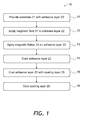
- a method 10 ( FIG. 1 ) of manufacturing an optically variable device 20 (the manufactured device is shown in FIG. 2H ) may include a step 11 of providing a substrate 21 with an adhesive layer 22 ( FIG. 2B ) on the substrate 21 ( FIGs. 2A, 2B ), which may be deposited, for example, by coating or printing.
- the substrate 21 may also be provided with the adhesive layer 22 already present on the substrate 21, and the adhesive 22 may require only activation, for example by heating.
- a magnetic field 31 ( FIG. 3A ) is applied, for example by providing a permanent magnet 30 ( FIGs. 2C and 3A ) under the substrate 21 ( FIGs. 2C and 3A ).
- An electromagnet may also be used.
- the magnetic field 31 generated by the magnet 30 extends through and over the adhesive layer 22 ( FIG. 3A ).
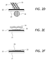
- magnetic flakes 23 are applied to the adhesive layer 22, for example, by blowing the magnetic flakes 23 onto the adhesive layer 22 using a stream 27 of gas e.g. air, argon, or nitrogen, having the magnetic flakes 23 suspended in the stream 27 of gas and carried by the stream 27 of gas, as shown schematically in FIG. 2D .
- the magnetic flakes 23 may be provided by dusting, or spreading the magnetic flakes 23 with the help of mechanical means, such as a blade, for example.
- the magnetic flakes 23 may adhere to the adhesive layer 22 ( FIG. 2E ).
- the magnetic field 31 causes the magnetic flakes 23 to become oriented or aligned along field lines 37 of the magnetic field 31 ( FIG. 3B ).
- the magnetic flakes 23 are applied to the adhesive layer 22 in presence of the magnetic field 31.
- the magnetic field 31 facilitates orientation of the magnetic flakes 23 during their flight towards the adhesive layer 22, so that the magnetic flakes 23 may land onto the adhesive layer 22 already oriented along the magnetic field 31 lines. If the magnetic field 31 is not applied in the flake application step 13, some of the magnetic flakes 23 may land flat on and adhere flat to the adhesive layer 22, which may make hinder their further orientation of the magnetic flakes 23 by the magnetic field 31.
- the adhesive layer 22 may be fully cured e.g. by applying heat 24 ( FIG. 2E ), ultraviolet (UV) light, etc., after application of the magnetic flakes 23 in the flake application step 13.
- the adhesive layer 22 may be already partially cured (partially uncured) prior to application of the magnetic flakes 23.
- the adhesive layer 22 having the magnetic flakes 23 adhered to the adhesive layer 22, or anchored in the adhesive layer 22, is coated with a coating layer 25 ( FIG. 2F ), for example a transparent adhesive layer or a varnish layer.
- the coating layer 25 may also include a semi-transparent colored layer in combination with the magnetic flakes 23, which may be colored or non-colored.
- the coating layer 25 is cured e.g. by applying heat 26, UV light, or both ( FIG. 2G ), so as to substantially preserve the orientation of the magnetic flakes 23 after the magnetic field 31 is removed.
- the adhesive layer 22 may also be fully cured, from a partially or fully uncured state.
- a second adhesive layer may be provided on top of the adhesive layer 22 or beside the adhesive layer 22.
- a second magnetic field may be applied to the second adhesive layer, and second magnetic flakes may be provided onto the second adhesive layer in the presence of the second magnetic field so that the second magnetic flakes oriented by the second magnetic field adhere to the second adhesive layer.
- the second magnetic flakes may also be absent a liquid carrier or binder.
- the second magnetic field may be different from the magnetic field 31, for example the second magnetic field may have a different orientation or strength, or field lines pattern.
- the second magnetic flakes may also be different from the magnetic flakes 23, for example the second magnetic flakes may have different color, size, material composition, etc. Magnetic fields and different flake types may be applied consecutively to obtain multi-color 3D indicia.
- the manufactured optically variable device 20 is shown in FIG. 2H .
- the optically variable device 20 includes the substrate 21, the adhesive layer 22 over the substrate 21, and the magnetic flakes 23 supported by the adhesive layer 22.
- the magnetic flakes 23 are adhered to the substrate 21, and may appear extending from the substrate 32.
- the magnetic flakes 23 are oriented by the magnetic field 31 ( FIGs. 3A and 3B ).
- the term "oriented" means that the magnetic flakes 23 are aligned, that is, disposed in a non-random, coordinated fashion.
- the coating layer 25 extends over the substrate 21 adjacent the adhesive layer 22, encapsulating the magnetic flakes 23.
- a portion 23A of the magnetic flake 23 is adhesively attached to the adhesive layer 22, and another portion 23B of the same magnetic flake 23 extends out of the adhesive layer 22 into the coating layer 25.
- the magnetic field 31 may be configured to have the field lines parallel to the surface of the substrate 21. Most of the flakes 23 planarized by the magnetic field 31 would have one major side in contact with the adhesive layer 22, and another major side in contact with the coating layer 25.
- the minimal thickness of the coating layer 25 is limited by size of individual flakes 23. For instance, for ⁇ 20 micrometer sized flakes, the coating layer 25 thickness may remain as small as 20-40 micrometers.
- the magnetic flakes 23 are applied to the adhesive layer 22 absent the coating layer 25. The magnetic flakes 23 may extend from the adhesive layer 22 e.g. by 15-20 micrometers.
- the coating layer 25 may be applied to the adhesive layer 22 in the coating step 15, to encapsulate the magnetic flakes 23 within the coating layer 25, which can remain as thin as 100 micrometers. It is preferred that the coating layer 25 be substantially transparent to visible light, being colorless or colored, depending on required optical performance of the optically variable device 20. Smaller magnetic flakes 23, for example having an average size of 5 to 10 micrometers, may be preferable, depending on a particular printing application.
- the magnetic flakes 23 may be reflective, e.g. the magnetic flakes 23 may have an optical reflectivity at visible wavelengths between 380nm and 750nm of at least 50%. Reflective magnetic flakes 23, when oriented, for example by a spherical or conical permanent magnet, may create a visual appearance of a metallic 3D-looking object, due to apparent reflectivity varying with illumination angle and, or observation angle.
- the magnetic flakes 23 may also include pearlescent or multilayer color-shifting coatings, which change color upon a change of angle of observation or illumination. Flakes which include multilayer color-shifting coatings may create a visual appearance of color-shifting 3D-looking objects, and may be particularly attractive for optical security applications.
- the magnetic flakes 23 may also have low reflectivity, so as to appear dark or black on a light background.
- the shape of 3D-looking objects depends on shape and magnetization direction of the magnet 30 placed under the substrate 21 ( FIG. 3A ).
- the magnet 30 may be shaped and oriented to create the magnetic field 31 of a particular configuration.
- the resulting 3D looking shape may be inverted by flipping over the structure of the optically variable device 20.
- an optically variable device 40 may be manufactured using the method 10 of FIG. 1 .
- a substrate 41 of the optically variable device 40 includes a release layer 41A.
- the coating layer 25 may be adhered to a second substrate 42 as shown in FIG. 4A .
- the release layer 41A may be then removed as shown in FIG. 4B , resulting in the optically variable device 40 being supported upside down by the second substrate 42, as shown in FIG. 4C .
- the adhesive layer 22 may include voids 22A in the adhesive layer 22, e.g. forming visible indicia such as the number "100", for example.
- the voids 22A in the adhesive layer 22 may be formed using any suitable method, such as silk screen printing or other printing methods, lithography, etc.
- the magnetic flakes applied to the voids 22A may be removed, for example, by directing a flow of gas on the voids 22A or by shaking. Masking may be applied while printing the adhesive, and, or providing the magnetic flakes 23, and, or providing further coating.
- the magnetic flakes 23 may optionally include a diffractive pattern and, or covert identification indicia discernible under magnification.
- FIG. 2H Several prototypes of the optically variable device 20 ( FIG. 2H ) have been manufactured, and optically variable performance of the prototypes has been evaluated.
- FIGs. 6A, 6B , and 7A-7C a plan-view photograph ( FIG. 6A ) of a prototype of the optically variable device 20 ( FIG. 2H ) is shown.
- the adhesive layer 22 of the prototype of FIG. 6A included an adhesive ink layer
- the magnetic flakes 23 included a color-shifting magnetic pigment changing color from gold at normal angle of viewing to green color at oblique angles.
- the coating layer 25 included varnish.
- the adhesive ink was cured prior to application of the varnish.
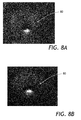
- FIG. 7A To provide a 3D appearance of a metal ball image 60 seen in the photograph of FIG. 6A , a spherical-cylindrical magnet pair including a spherical magnet 71 atop a cylindrical magnet 72 ( FIG. 7A ) has been placed under the optically variable device 20.
- the direction of viewing of FIG. 6A is shown in FIG. 7A at 74A.
- the direction of viewing 74A is shown in FIGs. 7A and 7B superimposed with the spherical 71 and cylindrical 72 magnets only to illustrate the geometry of the magnets in relation to the geometry of observation.
- the spherical 71-cylindrical 72 magnet pair was removed.
- FIG. 6B the same prototype is viewed at an oblique angle shown in FIG. 7B at 74B.
- FIG. 7C shows a plan view of the spherical 71-cylindrical 72 magnet pair.
- FIG. 8A, 8B , and 9A-9C a prototype of FIG. 8A has a similar layer structure as the prototype of FIG. 6A , the only difference being the position of the spherical magnet 71 ( FIG. 9A ) in the magnet pair used to orient the magnetic flakes 23 ( FIG. 2H ).
- FIG. 9A the direction of viewing is shown at 74A.
- the spherical magnet 71 is positioned close to an edge of the cylindrical magnet 72, resulting in a shifted position of a metal ball image 80 in FIGs. 8A and 8B .
- FIG. 8B the prototype of FIG. 8A is viewed at an oblique angle, as shown in FIG. 9B at 74B.
- FIG. 9C shows a plan view of the spherical 71-cylindrical 72 magnet pair.
- FIGs. 10A, 10B , and 11A-11C a prototype of FIG. 10A has a similar layer structure as the prototype of FIG. 6A , the only difference being that instead of the spherical 71- cylindrical 72 magnet pair, a cylindrical 111 - rectangular 112 magnet pair ( FIGs. 11A-11C ) is used to orient the magnetic flakes 23 ( FIG. 2H ) to form an image of a 3D cone 100 within a round-cornered rectangle 101 ( FIGs. 10A, 10B ).
- the direction of viewing corresponding to FIG. 10A is shown at in FIG. 11A at 74A.
- FIG. 10B the same prototype is viewed at an oblique viewing angle shown in FIG. 11B at 74B.
- FIG. 11C shows a plan view of the cylindrical 111 - rectangular 112 magnet pair.
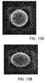
- the cylindrical 111 - rectangular 112 magnet pair shown in FIGs. 11A-11C has been used to orient the magnetic flakes 23 in prototypes of FIGs. 12A, 12B , 13A, 13B , 14A, and 14B described below. These prototypes have been manufactured with different layer materials, using varying layer curing schedules.
- the adhesive layer 22 ( FIG. 2H ) included not adhesive ink but a same varnish material as the coating layer 25.
- the varnish of the adhesive layer 22 was cured after application of the Go/Gr color-shifting magnetic pigment flakes. The 3D effect was present, as can be seen by comparing FIGs. 12A and 12B , when the varnish was used in the adhesive layer 22.
- a UV-curable adhesive ink was used to form the adhesive layer 22.
- the UV-curable adhesive ink was pre-cured by UV light prior to application of achromatic magnetic flakes 23, which included 5 layers MgF 2 /Al/magnetic layer/Al/MgF 2 .
- the 3D cone was not observed.
- the UV-curable adhesive ink was not pre-cured prior to application of the achromatic magnetic flakes 23. Rather, the UV-curable adhesive ink was cured after the application of the achromatic magnetic flakes 23.
Abstract
Description
- The present disclosure relates to optically variable devices, and in particular to optically variable devices including magnetically alignable flakes.
- Optically variable devices are optical devices whose optical performance depends on angle of incidence of illuminating light or angle of observation. A common example of an optically variable device is an iridescent security feature used as an anti-counterfeiting measure on banknotes, credit cards, stock certificates, government-issued identification documents, etc. An optically variable device may provide a visually varying image, for example an illusory three-dimensional (3D) image, a color-shifting image, or both. Such an image is difficult to counterfeit without knowledge of a specific recipe used to manufacture the optical variable device providing the image.
- Optically variable devices may be made by coating a surface with an ink or paint including flat platelet-like reflective and, or color-shifting particles. Such surfaces show higher reflectance and brighter colors than surfaces coated with a paint or ink containing conventional pigments. Substrates painted or printed with color-shifting flaked pigments may show change of color when viewed at different angles.
- Flaked pigments may contain a material that is magnetically sensitive, so as to be alignable or orientable in an applied magnetic field. Such flakes may be manufactured from a combination of magnetic and non-magnetic materials and mixed with a paint or ink vehicle in the production of magnetic paints or inks. A feature of these products is the ability of the flakes to become oriented along the lines of an applied field inside of a layer of liquid paint or ink, while substantially remaining in this position after drying or curing of the paint or ink vehicle. Relative orientation of the flake and its major dimension with respect to the coated surface determines the level of reflectance or its direction and, or may determine angle-dependent color or brightness of the paint or ink.
- By way of example,
Phillips et al. in US Patent 6,808,806 disclose methods and devices for producing color-shifting images on coated articles using magnetically alignable flakes including color-shifting coatings. The color-shifting images are defined by the magnetic field applied to the coatings as the coatings are dried or cured. For example, a sheet magnet shaped as a symbol, a letter, or another indicia may be brought in close proximity to the coating during cure. After the coating is cured, the sheet magnet is removed, and the indicia may be seen as a color-shifting image on the coating. The magnetic field application may be adapted for modern printing environments; for example,Raksha et al. in US Patent Application Publication 2005/0106367 disclose a method and apparatus for orienting magnetic flakes in high-speed, linear printing operation. - A 3D illusive image may also be formed on the painted product by applying a spatially varying magnetic field to the surface of the product while the paint still is in the liquid state. When the paint is cured and the magnetic field is removed, the 3D illusive image remains visible on the surface of the painted product. The 3D illusive image appears because light rays incident on the paint layer are influenced differently by differently oriented magnetic particles.
Raksha et al. in US Patent 7,934,451 disclose a method and apparatus to orient magnetic flakes in desired 3D patterns in a high-speed linear printing apparatus. - Despite interesting and often intriguing optical effects produced by solidified suspensions of magnetic flakes, their application in optical security devices has been somewhat limited, in particular for banknotes. The application of magnetically alignable flake suspensions in banknotes and other valuable documents may be hindered by a poor compatibility of two main printing processes mostly used in manufacturing of banknotes - offset printing and Intaglio printing - with magnetically alignable particle suspensions. An offset printing process typically produces a very thin ink film thickness, and as such, cannot transfer large magnetic particles, for example particles that are 30 micrometers in size. An Intaglio printing process typically uses a highly viscous ink, which does not allow efficient alignment of magnetic particles suspended in the ink, at least without taking special measures to lessen the viscosity of the ink while applying a magnetic field, as is disclosed by
Raksha et al. in US Patent 8,211,509 . - In accordance with an aspect of the disclosure, a thickness of a layer including oriented magnetic flakes may be reduced by applying magnetic flakes absent any liquid binder or carrier to an adhesive surface in the presence of magnetic field, which orients the magnetic flakes. For example, magnetic particles may be dusted or blown onto an adhesive surface in the presence of the magnetic field, causing the magnetic flakes to adhere to the adhesive surface in an oriented manner. Then, a thin coating layer may be applied to the oriented magnetic particles adhered to the adhesive surface. The coating layer is cured to maintain the orientation of the magnetic flakes.
- In accordance with an aspect of the disclosure, there is provided a method of manufacturing an optically variable device, the method comprising:
- providing a substrate with an first adhesive layer thereon;
- applying a first magnetic field to the first adhesive layer and providing magnetic flakes absent a liquid carrier or binder onto the first adhesive layer in the presence of the first magnetic field so that the magnetic flakes oriented by the first magnetic field adhere to the first adhesive layer;
coating the first adhesive layer and the magnetic flakes adhered thereto with a coating layer; and
curing the coating layer, so as to substantially maintain orientation of the magnetic flakes. - The first adhesive layer may be only partially cured during depositing the magnetic flakes thereon. The substrate may include a release layer, in which case the coating layer may be adhered to a second substrate, and the release layer may be removed, to obtain a "flipped" orientation pattern of the magnetic flakes. The method may be adaptable to high printing speeds.
- In one embodiment, a second adhesive layer may be provided on top of the first adhesive layer or beside the first adhesive layer. A second magnetic field may be applied to the second adhesive layer, and second magnetic flakes absent a liquid carrier or binder may be provided onto the second adhesive layer in the presence of the second magnetic field, so that the second magnetic flakes oriented by the second magnetic field adhere to the second adhesive layer. After this, the second adhesive layer may be cured.
- In accordance with the disclosure, there is further provided a method of manufacturing an optically variable device, the method comprising:
providing a substrate with an adhesive layer thereon;
applying a magnetic field to the adhesive layer;
separately applying magnetic flakes and a coating to the adhesive layer, by initially applying the magnetic flakes absent a liquid carrier, causing the magnetic flakes to adhere to the adhesive layer, wherein the magnetic flakes adhered to the adhesive layer are oriented by the magnetic field; and, after the magnetic flakes have been applied to the adhesive layer, applying the coating to the adhesive layer so as to form a coating layer on the adhesive layer, wherein the coating layer encapsulates the magnetic flakes; and
curing the coating layer, so as to substantially maintain orientation of the magnetic flakes. - In accordance with the disclosure, there is further provided an optically variable device comprising a substrate; an adhesive layer over the substrate; a plurality of oriented magnetic flakes supported by the adhesive layer; and a coating layer over the substrate adjacent the adhesive layer. The coating may encapsulate the magnetic flakes extending from the adhesive layer, so that a portion of each one of the plurality of oriented magnetic flakes is adhesively attached to the adhesive layer, and a remaining portion of the same magnetic flake extends out of the adhesive layer into the coating layer.
- In one embodiment, the adhesive layer is disposed on the substrate, and the coating layer is disposed on the adhesive layer. The coating covering the flakes on the adhesive layer may be of the same material as the adhesive layer, or may be a different material. The magnetic flakes may be partially disposed in the adhesive layer. In one embodiment, the magnetic flakes are reflective, and may include color-shifting multilayer coatings. By carefully selecting magnets to generate the magnetic fields, the magnetic flakes may be oriented so as to create a visual appearance of a 3D object such as a hemisphere, a cone, a funnel, a combination of different images obtained at separated stations, etc. The magnetic alignment may be repeated to create other images on top or aside a first image.
- Exemplary embodiments will now be described in conjunction with the drawings, in which:
-
FIG. 1 is a flow chart of a method of manufacturing an optically varying device according to the present disclosure; -
FIGs. 2A-2H are side cross-sectional views of an optically variable device of the present disclosure at different progressive stages of manufacturing; -
FIG. 2I is a magnified view of a single flake of the optically variable device ofFIG. 2H , attached to an adhesive layer; -
FIG. 3A is a schematic side cross-sectional view of a magnet underneath a substrate, showing lines of magnetic field of the magnet; -
FIG. 3B is a schematic side cross-sectional view of a substrate supporting magnetic flakes aligned along the magnetic field lines of the magnet shown inFIG. 3A ; -
FIGs. 4A to 4C are side cross-sectional views of an inverted optically variable device of the present disclosure at different progressive stages of manufacturing; -
FIG. 5 is a schematic plan view of an optically varying device, in which the adhesive layer is patterned to form a banknote denomination "100"; -
FIG. 6A is a plan-view photograph of an optically variable device, in which magnetic flakes have been aligned on a layer of adhesive ink with a spherical-cylindrical magnet pair including a cylindrical magnet and a spherical magnet centered on top of the cylindrical magnet; -
FIG. 6B is an oblique-view photograph of the optically variable device ofFIG. 6A ; -
FIG. 7A is a side cross-sectional view of the spherical-cylindrical magnet pair used to align magnetic flakes of the prototypes ofFIGs. 6A and 6B , showing a viewing direction ofFIG. 6A ; -
Fig. 7B is a side cross-sectional view of the spherical-cylindrical magnet pair used to align magnetic flakes of the prototypes ofFIGs. 6A and 6B , showing a viewing direction ofFIG. 6B ; -
FIG. 7C is a top view of the spherical-cylindrical magnet pair used to align magnetic flakes of the prototypes ofFIGs. 6A and 6B ; -
FIG. 8A is a plan-view photograph of an optically variable device, in which magnetic flakes have been aligned on a layer of adhesive ink with a spherical-cylindrical magnet pair including a spherical magnet atop of and near an edge of a cylindrical magnet; -
FIG. 8B is an oblique-view photograph of the optically variable device ofFIG. 8A ; -
FIG. 9A is a side cross-sectional view of the spherical-cylindrical magnet pair used to align magnetic flakes of the prototypes ofFIGs. 8A and 8B , showing a viewing direction ofFIG. 8A ; -
Fig. 9B is a side cross-sectional view of the spherical-cylindrical magnet pair used to align magnetic flakes of the prototypes ofFIGs. 8A and 8B , showing a viewing direction ofFIG. 8B ; -
FIG. 9C is a plan view of the spherical-cylindrical magnet pair used to align magnetic flakes of the prototypes ofFIGs. 8A and 8B ; -
FIG. 10A is a plan-view photograph of an optically variable device, in which magnetic flakes have been aligned on a layer of adhesive ink with a cylindrical-rectangular magnet pair including a cylindrical magnet on top of a rectangular magnet; -
FIG. 10B is an oblique-view photograph of the optically variable device ofFIG. 10A ; -
FIG. 11A is a side cross-sectional view of the cylindrical-rectangular magnet pair used to align magnetic flakes of the prototypes ofFIGs. 10A and 10B , showing a viewing direction ofFIG. 10A ; -
Fig. 11B is a side cross-sectional view of the cylindrical-rectangular magnet pair used to align magnetic flakes of the prototypes ofFIGs. 10A and 10B , showing a viewing direction ofFIG. 10B ; -
FIG. 11C is a plan view of the cylindrical-rectangular magnet pair used to align magnetic flakes of the prototypes ofFIGs. 10A and 10B ; -
FIG. 12A is a plan-view photograph of an optically variable device, in which magnetic flakes have been aligned on a layer of varnish with the cylindrical-rectangular magnet pair ofFIGs. 11A-11C ; -
FIG. 12B is an oblique-view photograph of the optically variable device ofFIG. 12A ; -
FIG. 13A is a plan-view photograph of an optically variable device, in which magnetic flakes have been applied to a layer of a UV-cured adhesive ink with the cylindrical-rectangular magnet pair ofFIGs. 11A-11C ; -
FIG. 13B is an oblique-view photograph of the optically variable device ofFIG. 13A ; -
FIG. 14A is a plan-view photograph of an optically variable device, in which magnetic flakes have been applied to a layer of an uncured adhesive ink with the rectangular-cylindrical magnet pair ofFIGs. 11A-11C ; and -
FIG. 14B is an oblique-view photograph of the optically variable device ofFIG. 14A . - While the present teachings are described in conjunction with various embodiments and examples, it is not intended that the present teachings be limited to such embodiments. On the contrary, the present teachings encompass various alternatives and equivalents, as will be appreciated by those of skill in the art.
- Referring to
FIG. 1 with further reference toFIGs. 2A-2H ,3A, and 3B , a method 10 (FIG. 1 ) of manufacturing an optically variable device 20 (the manufactured device is shown inFIG. 2H ) may include astep 11 of providing asubstrate 21 with an adhesive layer 22 (FIG. 2B ) on the substrate 21 (FIGs. 2A, 2B ), which may be deposited, for example, by coating or printing. Thesubstrate 21 may also be provided with theadhesive layer 22 already present on thesubstrate 21, and the adhesive 22 may require only activation, for example by heating. In a magneticfield application step 12, a magnetic field 31 (FIG. 3A ) is applied, for example by providing a permanent magnet 30 (FIGs. 2C and3A ) under the substrate 21 (FIGs. 2C and3A ). An electromagnet may also be used. Themagnetic field 31 generated by themagnet 30 extends through and over the adhesive layer 22 (FIG. 3A ). - In a
flake application step 13,magnetic flakes 23 are applied to theadhesive layer 22, for example, by blowing themagnetic flakes 23 onto theadhesive layer 22 using astream 27 of gas e.g. air, argon, or nitrogen, having themagnetic flakes 23 suspended in thestream 27 of gas and carried by thestream 27 of gas, as shown schematically inFIG. 2D . Alternatively, themagnetic flakes 23 may be provided by dusting, or spreading themagnetic flakes 23 with the help of mechanical means, such as a blade, for example. Upon reaching theadhesive layer 22, themagnetic flakes 23 may adhere to the adhesive layer 22 (FIG. 2E ). Themagnetic field 31 causes themagnetic flakes 23 to become oriented or aligned alongfield lines 37 of the magnetic field 31 (FIG. 3B ). - Preferably, the
magnetic flakes 23 are applied to theadhesive layer 22 in presence of themagnetic field 31. In case of dusting of deposition with gaseous stream, themagnetic field 31 facilitates orientation of themagnetic flakes 23 during their flight towards theadhesive layer 22, so that themagnetic flakes 23 may land onto theadhesive layer 22 already oriented along themagnetic field 31 lines. If themagnetic field 31 is not applied in theflake application step 13, some of themagnetic flakes 23 may land flat on and adhere flat to theadhesive layer 22, which may make hinder their further orientation of themagnetic flakes 23 by themagnetic field 31. - In an optional adhesive
layer curing step 14 of the method 10 (FIG. 1 ), theadhesive layer 22 may be fully cured e.g. by applying heat 24 (FIG. 2E ), ultraviolet (UV) light, etc., after application of themagnetic flakes 23 in theflake application step 13. Theadhesive layer 22 may be already partially cured (partially uncured) prior to application of themagnetic flakes 23. - In a
coating step 15 of the method 10 (FIG. 1 ), theadhesive layer 22 having themagnetic flakes 23 adhered to theadhesive layer 22, or anchored in theadhesive layer 22, is coated with a coating layer 25 (FIG. 2F ), for example a transparent adhesive layer or a varnish layer. Thecoating layer 25 may also include a semi-transparent colored layer in combination with themagnetic flakes 23, which may be colored or non-colored. In a curingstep 16, thecoating layer 25 is cured e.g. by applyingheat 26, UV light, or both (FIG. 2G ), so as to substantially preserve the orientation of themagnetic flakes 23 after themagnetic field 31 is removed. In this step, theadhesive layer 22 may also be fully cured, from a partially or fully uncured state. - A second adhesive layer, not shown, may be provided on top of the
adhesive layer 22 or beside theadhesive layer 22. A second magnetic field, not shown, may be applied to the second adhesive layer, and second magnetic flakes may be provided onto the second adhesive layer in the presence of the second magnetic field so that the second magnetic flakes oriented by the second magnetic field adhere to the second adhesive layer. The second magnetic flakes may also be absent a liquid carrier or binder. The second magnetic field may be different from themagnetic field 31, for example the second magnetic field may have a different orientation or strength, or field lines pattern. The second magnetic flakes may also be different from themagnetic flakes 23, for example the second magnetic flakes may have different color, size, material composition, etc. Magnetic fields and different flake types may be applied consecutively to obtain multi-color 3D indicia. - The manufactured optically
variable device 20 is shown inFIG. 2H . The opticallyvariable device 20 includes thesubstrate 21, theadhesive layer 22 over thesubstrate 21, and themagnetic flakes 23 supported by theadhesive layer 22. Themagnetic flakes 23 are adhered to thesubstrate 21, and may appear extending from the substrate 32. Themagnetic flakes 23 are oriented by the magnetic field 31 (FIGs. 3A and 3B ). Herein, the term "oriented" means that themagnetic flakes 23 are aligned, that is, disposed in a non-random, coordinated fashion. Thecoating layer 25 extends over thesubstrate 21 adjacent theadhesive layer 22, encapsulating themagnetic flakes 23. As seen inFIG 2I , aportion 23A of themagnetic flake 23 is adhesively attached to theadhesive layer 22, and anotherportion 23B of the samemagnetic flake 23 extends out of theadhesive layer 22 into thecoating layer 25. In one embodiment, themagnetic field 31 may be configured to have the field lines parallel to the surface of thesubstrate 21. Most of theflakes 23 planarized by themagnetic field 31 would have one major side in contact with theadhesive layer 22, and another major side in contact with thecoating layer 25. - Application of the
magnetic flakes 23 and thecoating layer 25 in separate steps may enable resulting opticallyvariable devices 20 to remain quite thin. Essentially, the minimal thickness of thecoating layer 25 is limited by size ofindividual flakes 23. For instance, for <20 micrometer sized flakes, thecoating layer 25 thickness may remain as small as 20-40 micrometers. In theflake application step 13, themagnetic flakes 23 are applied to theadhesive layer 22 absent thecoating layer 25. Themagnetic flakes 23 may extend from theadhesive layer 22 e.g. by 15-20 micrometers. Once themagnetic flakes 23 adhere to theadhesive layer 22, being oriented along the field lines 37 of themagnetic field 31, thecoating layer 25 may be applied to theadhesive layer 22 in thecoating step 15, to encapsulate themagnetic flakes 23 within thecoating layer 25, which can remain as thin as 100 micrometers. It is preferred that thecoating layer 25 be substantially transparent to visible light, being colorless or colored, depending on required optical performance of the opticallyvariable device 20. Smallermagnetic flakes 23, for example having an average size of 5 to 10 micrometers, may be preferable, depending on a particular printing application. - The
magnetic flakes 23 may be reflective, e.g. themagnetic flakes 23 may have an optical reflectivity at visible wavelengths between 380nm and 750nm of at least 50%. Reflectivemagnetic flakes 23, when oriented, for example by a spherical or conical permanent magnet, may create a visual appearance of a metallic 3D-looking object, due to apparent reflectivity varying with illumination angle and, or observation angle. Themagnetic flakes 23 may also include pearlescent or multilayer color-shifting coatings, which change color upon a change of angle of observation or illumination. Flakes which include multilayer color-shifting coatings may create a visual appearance of color-shifting 3D-looking objects, and may be particularly attractive for optical security applications. Themagnetic flakes 23 may also have low reflectivity, so as to appear dark or black on a light background. - The shape of 3D-looking objects depends on shape and magnetization direction of the
magnet 30 placed under the substrate 21 (FIG. 3A ). Themagnet 30 may be shaped and oriented to create themagnetic field 31 of a particular configuration. Furthermore, the resulting 3D looking shape may be inverted by flipping over the structure of the opticallyvariable device 20. - Turning to
FIGs. 4A-4C with further reference toFIG. 1 , an opticallyvariable device 40 may be manufactured using the method 10 ofFIG. 1 . Asubstrate 41 of the opticallyvariable device 40 includes arelease layer 41A. Thecoating layer 25 may be adhered to asecond substrate 42 as shown inFIG. 4A . Therelease layer 41A may be then removed as shown inFIG. 4B , resulting in the opticallyvariable device 40 being supported upside down by thesecond substrate 42, as shown inFIG. 4C . - Referring to
FIG. 5 , theadhesive layer 22 may includevoids 22A in theadhesive layer 22, e.g. forming visible indicia such as the number "100", for example. Thevoids 22A in theadhesive layer 22 may be formed using any suitable method, such as silk screen printing or other printing methods, lithography, etc. Once themagnetic flakes 23 are applied to theadhesive layer 22 in theflake application step 13 of the method 10, the magnetic flakes applied to thevoids 22A may be removed, for example, by directing a flow of gas on thevoids 22A or by shaking. Masking may be applied while printing the adhesive, and, or providing themagnetic flakes 23, and, or providing further coating. For added security, themagnetic flakes 23 may optionally include a diffractive pattern and, or covert identification indicia discernible under magnification. - Several prototypes of the optically variable device 20 (
FIG. 2H ) have been manufactured, and optically variable performance of the prototypes has been evaluated. Referring toFIGs. 6A, 6B , and7A-7C , with further reference toFIG. 2H , a plan-view photograph (FIG. 6A ) of a prototype of the optically variable device 20 (FIG. 2H ) is shown. Theadhesive layer 22 of the prototype ofFIG. 6A included an adhesive ink layer, themagnetic flakes 23 included a color-shifting magnetic pigment changing color from gold at normal angle of viewing to green color at oblique angles. Thecoating layer 25 included varnish. The adhesive ink was cured prior to application of the varnish. - To provide a 3D appearance of a
metal ball image 60 seen in the photograph ofFIG. 6A , a spherical-cylindrical magnet pair including aspherical magnet 71 atop a cylindrical magnet 72 (FIG. 7A ) has been placed under the opticallyvariable device 20. The direction of viewing ofFIG. 6A is shown inFIG. 7A at 74A. The direction of viewing 74A is shown inFIGs. 7A and 7B superimposed with the spherical 71 and cylindrical 72 magnets only to illustrate the geometry of the magnets in relation to the geometry of observation. For an actual observation, the spherical 71-cylindrical 72 magnet pair was removed. InFIG. 6B , the same prototype is viewed at an oblique angle shown inFIG. 7B at 74B.FIG. 7C shows a plan view of the spherical 71-cylindrical 72 magnet pair. - Referring to
FIGs. 8A, 8B , and9A-9C , with further reference toFIGs. 2H and6A , a prototype ofFIG. 8A has a similar layer structure as the prototype ofFIG. 6A , the only difference being the position of the spherical magnet 71 (FIG. 9A ) in the magnet pair used to orient the magnetic flakes 23 (FIG. 2H ). InFIG. 9A , the direction of viewing is shown at 74A. InFIGs. 9A and 9B , thespherical magnet 71 is positioned close to an edge of thecylindrical magnet 72, resulting in a shifted position of ametal ball image 80 inFIGs. 8A and 8B . InFIG. 8B , the prototype ofFIG. 8A is viewed at an oblique angle, as shown inFIG. 9B at 74B.FIG. 9C shows a plan view of the spherical 71-cylindrical 72 magnet pair. - Turning to
FIGs. 10A, 10B , and11A-11C , with further reference toFIGs. 2H and6A , a prototype ofFIG. 10A has a similar layer structure as the prototype ofFIG. 6A , the only difference being that instead of the spherical 71- cylindrical 72 magnet pair, a cylindrical 111 - rectangular 112 magnet pair (FIGs. 11A-11C ) is used to orient the magnetic flakes 23 (FIG. 2H ) to form an image of a3D cone 100 within a round-cornered rectangle 101 (FIGs. 10A, 10B ). The direction of viewing corresponding toFIG. 10A is shown at inFIG. 11A at 74A. InFIG. 10B , the same prototype is viewed at an oblique viewing angle shown inFIG. 11B at 74B.FIG. 11C shows a plan view of the cylindrical 111 - rectangular 112 magnet pair. - The cylindrical 111 - rectangular 112 magnet pair shown in
FIGs. 11A-11C has been used to orient themagnetic flakes 23 in prototypes ofFIGs. 12A, 12B ,13A, 13B ,14A, and 14B described below. These prototypes have been manufactured with different layer materials, using varying layer curing schedules. - In a prototype shown in
FIGs.12A and 12B , the adhesive layer 22 (FIG. 2H ) included not adhesive ink but a same varnish material as thecoating layer 25. The varnish of theadhesive layer 22 was cured after application of the Go/Gr color-shifting magnetic pigment flakes. The 3D effect was present, as can be seen by comparingFIGs. 12A and 12B , when the varnish was used in theadhesive layer 22. - In a prototype shown in
FIGs. 13A and 13B , a UV-curable adhesive ink was used to form theadhesive layer 22. The UV-curable adhesive ink was pre-cured by UV light prior to application of achromaticmagnetic flakes 23, which included 5 layers MgF2/Al/magnetic layer/Al/MgF2. The 3D cone was not observed. In a prototype shown inFIGs. 14A and 14B , the UV-curable adhesive ink was not pre-cured prior to application of the achromaticmagnetic flakes 23. Rather, the UV-curable adhesive ink was cured after the application of the achromaticmagnetic flakes 23. 3D cone features 141A (FIG. 14A ) and 141B (FIG. 14B ) were observed with this prototype. Therefore, it may be preferable to cure the adhesive layer 22 (FIG. 2E and step 14 of the method 10 ofFIG. 1 ) after application of themagnetic flakes 23 on the adhesive layer 22 (FIG. 2D and step 13 of the method 10 ofFIG. 1 ). - The present disclosure is not to be limited in scope by the specific embodiments described herein. Indeed, other various embodiments and modifications, in addition to those described herein, will be apparent to those of ordinary skill in the art from the foregoing description and accompanying drawings. Thus, such other embodiments and modifications are intended to fall within the scope of the present disclosure. Further, although the present disclosure has been described herein in the context of a particular implementation in a particular environment for a particular purpose, those of ordinary skill in the art will recognize that its usefulness is not limited thereto and that the present disclosure may be beneficially implemented in any number of environments for any number of purposes. Accordingly, the claims set forth below should be construed in view of the full breadth and spirit of the present disclosure as described herein.
Claims (15)
- A method of manufacturing an optically variable device, the method comprising:providing a substrate with an first adhesive layer thereon;applying a first magnetic field to the first adhesive layer and providing magnetic flakes absent a liquid carrier or binder onto the first adhesive layer in the presence of the first magnetic field so that the magnetic flakes oriented by the first magnetic field adhere to the first adhesive layer;coating the first adhesive layer and the magnetic flakes adhered thereto with a coating layer; andcuring the coating layer, so as to substantially maintain orientation of the magnetic flakes.
- The method of claim 1, wherein the first adhesive layer is at least partially uncured when the magnetic flakes are provided onto the first adhesive layer, the method further comprising curing the first adhesive layer after the magnetic flakes have adhered thereto.
- The method of claim 2, wherein the adhesive and coating layers are cured together.
- The method of claim 1, wherein the first magnetic field is created by a permanent magnet selected to provide a visual appearance of a 3D object on or within the optically variable device.
- The method of any one of claims 1 to 4, wherein the magnetic flakes are provided onto the first adhesive layer while applying the first magnetic field.
- The method of claim 5, wherein the magnetic flakes are provided onto the first adhesive layer by blowing the magnetic flakes onto the first adhesive layer using a stream of gas comprising the magnetic flakes suspended therein.
- The method of claim 1, wherein the first adhesive layer comprises voids therein, the method further comprising removing magnetic flakes from the voids by directing a flow of gas on the voids.
- The method of claim 1, wherein the magnetic flakes comprise a multilayer color shifting coating.
- The method of claim 1, wherein the substrate comprises a release layer, the method further comprising adhering the coating layer to a second substrate and removing the release layer.
- The method of claim 1, further comprising providing a second adhesive layer on top of the first adhesive layer or beside the first adhesive layer;
applying a second magnetic field to the second adhesive layer, and providing second magnetic flakes absent a liquid carrier or binder onto the second adhesive layer in the presence of the second magnetic field so that the second magnetic flakes oriented by the second magnetic field adhere to the second adhesive layer; and
curing the second adhesive layer. - The method of claim 10, wherein the second magnetic field is different from the first magnetic field, or wherein the second magnetic flakes are different from the first magnetic flakes.
- The method of claim 1, wherein the coating layer is colored.
- An optically variable device comprising:a substrate;an adhesive layer over the substrate;a plurality of oriented magnetic flakes supported by the adhesive layer; anda coating layer over the substrate adjacent the adhesive layer, wherein the coating encapsulates the magnetic flakes extending from the adhesive layer, wherein a portion of each one of the plurality of oriented magnetic flakes is adhesively attached to the adhesive layer, and a remaining portion of the same magnetic flake extends out of the adhesive layer into the coating layer.
- The optically variable device of claim 13, wherein at least some of the plurality of oriented magnetic flakes comprise a multilayer color-shifting coating.
- The optically variable device of claim 13 or claim 14, wherein the plurality of the oriented magnetic flakes are oriented so as to create a visual appearance of a 3D object.
Priority Applications (1)
| Application Number | Priority Date | Filing Date | Title |
|---|---|---|---|
| EP19159771.5A EP3527293A1 (en) | 2014-05-12 | 2015-05-12 | Optically variable device comprising magnetic flakes |
Applications Claiming Priority (1)
| Application Number | Priority Date | Filing Date | Title |
|---|---|---|---|
| US201461992093P | 2014-05-12 | 2014-05-12 |
Related Child Applications (2)
| Application Number | Title | Priority Date | Filing Date |
|---|---|---|---|
| EP19159771.5A Division-Into EP3527293A1 (en) | 2014-05-12 | 2015-05-12 | Optically variable device comprising magnetic flakes |
| EP19159771.5A Division EP3527293A1 (en) | 2014-05-12 | 2015-05-12 | Optically variable device comprising magnetic flakes |
Publications (3)
| Publication Number | Publication Date |
|---|---|
| EP2944381A2 true EP2944381A2 (en) | 2015-11-18 |
| EP2944381A3 EP2944381A3 (en) | 2016-01-20 |
| EP2944381B1 EP2944381B1 (en) | 2019-04-17 |
Family
ID=53672984
Family Applications (2)
| Application Number | Title | Priority Date | Filing Date |
|---|---|---|---|
| EP19159771.5A Pending EP3527293A1 (en) | 2014-05-12 | 2015-05-12 | Optically variable device comprising magnetic flakes |
| EP15167387.8A Active EP2944381B1 (en) | 2014-05-12 | 2015-05-12 | Optically variable device comprising magnetic flakes |
Family Applications Before (1)
| Application Number | Title | Priority Date | Filing Date |
|---|---|---|---|
| EP19159771.5A Pending EP3527293A1 (en) | 2014-05-12 | 2015-05-12 | Optically variable device comprising magnetic flakes |
Country Status (5)
| Country | Link |
|---|---|
| US (2) | US9827805B2 (en) |
| EP (2) | EP3527293A1 (en) |
| CN (2) | CN109291608A (en) |
| DK (1) | DK2944381T3 (en) |
| HK (1) | HK1217674A1 (en) |
Cited By (1)
| Publication number | Priority date | Publication date | Assignee | Title |
|---|---|---|---|---|
| WO2018054819A1 (en) * | 2016-09-22 | 2018-03-29 | Sicpa Holding Sa | Apparatuses and processes for producing optical effect layers comprising oriented non-spherical magnetic or magnetizable pigment particles |
Families Citing this family (5)
| Publication number | Priority date | Publication date | Assignee | Title |
|---|---|---|---|---|
| US10357991B2 (en) | 2016-12-19 | 2019-07-23 | Viavi Solutions Inc. | Security ink based security feature |
| CN109094231B (en) * | 2018-06-27 | 2021-11-19 | 中山市三盛化工科技有限公司 | Magnetic three-dimensional printing process |
| EP3826852B1 (en) * | 2018-07-25 | 2022-08-03 | Koenig & Bauer AG | Devices for aligning magnetic or magnetizable particles and machine for generating optically variable image elements |
| EP3959080A4 (en) * | 2019-04-26 | 2022-12-21 | Viavi Solutions Inc. | Optical device with magnetic flakes and structured substrate |
| CN110498943B (en) * | 2019-08-26 | 2021-10-19 | 哈尔滨工程大学 | Preparation method of anisotropic surface with controllable laminated structure |
Citations (4)
| Publication number | Priority date | Publication date | Assignee | Title |
|---|---|---|---|---|
| US6808806B2 (en) | 2001-05-07 | 2004-10-26 | Flex Products, Inc. | Methods for producing imaged coated articles by using magnetic pigments |
| US20050106367A1 (en) | 2002-07-15 | 2005-05-19 | Jds Uniphase Corporation | Method and apparatus for orienting magnetic flakes |
| US7934451B2 (en) | 2002-07-15 | 2011-05-03 | Jds Uniphase Corporation | Apparatus for orienting magnetic flakes |
| US8211509B2 (en) | 2002-07-15 | 2012-07-03 | Raksha Vladimir P | Alignment of paste-like ink having magnetic particles therein, and the printing of optical effects |
Family Cites Families (19)
| Publication number | Priority date | Publication date | Assignee | Title |
|---|---|---|---|---|
| BE468354A (en) * | 1945-10-08 | 1900-01-01 | ||
| GB1428138A (en) * | 1972-10-03 | 1976-03-17 | ||
| US5171363A (en) * | 1979-12-28 | 1992-12-15 | Flex Products, Inc. | Optically variable printing ink |
| US6103361A (en) | 1997-09-08 | 2000-08-15 | E. I. Du Pont De Nemours And Company | Patterned release finish |
| US7047883B2 (en) | 2002-07-15 | 2006-05-23 | Jds Uniphase Corporation | Method and apparatus for orienting magnetic flakes |
| US7258900B2 (en) * | 2002-07-15 | 2007-08-21 | Jds Uniphase Corporation | Magnetic planarization of pigment flakes |
| US20100208351A1 (en) * | 2002-07-15 | 2010-08-19 | Nofi Michael R | Selective and oriented assembly of platelet materials and functional additives |
| TWI402106B (en) | 2005-04-06 | 2013-07-21 | Jds Uniphase Corp | Dynamic appearance-changing optical devices (dacod) printed in a shaped magnetic field including printable fresnel structures |
| US7420663B2 (en) | 2005-05-24 | 2008-09-02 | Bwt Property Inc. | Spectroscopic sensor on mobile phone |
| DK1745940T3 (en) | 2005-07-20 | 2014-03-03 | Jds Uniphase Corp | Two-step FOR COATING OF AN OBJECT OF SAFETY PRESSURE |
| CA2580321C (en) * | 2006-03-06 | 2014-11-04 | Jds Uniphase Corporation | Security devices incorporating optically variable adhesive |
| TWI437059B (en) * | 2006-07-12 | 2014-05-11 | Jds Uniphase Corp | Stamping a coating of cured field aligned special effect flakes and image formed thereby |
| AU2008219354B2 (en) | 2007-09-19 | 2014-02-13 | Viavi Solutions Inc. | Anisotropic magnetic flakes |
| DE602007010476D1 (en) | 2007-11-22 | 2010-12-23 | Jds Uniphase Corp | Provide borders or borders around opaque flakes for hidden security applications |
| AU2010277718B2 (en) * | 2009-07-28 | 2014-09-11 | Sicpa Holding Sa | Transfer foil comprising optically variable magnetic pigment, method of making, use of transfer foil, and article or document comprising such |
| US8511712B2 (en) | 2009-11-24 | 2013-08-20 | Jds Uniphase Corporation | Mixture of magnetically orientable color shifting flakes and non-magnetically orientable color shifting flakes exhibiting a common color |
| US20120001116A1 (en) | 2010-06-30 | 2012-01-05 | Jds Uniphase Corporation | Magnetic multilayer pigment flake and coating composition |
| DK2484455T3 (en) * | 2011-02-07 | 2015-03-09 | Sicpa Holding Sa | A device for displaying a dynamic visual movement effect and process for producing same |
| CN103058878B (en) * | 2013-01-14 | 2014-08-13 | 聂世保 | 1, 3-allyl ethylene diamine tetraacetic acid as well as preparation method and application thereof |
-
2015
- 2015-05-11 CN CN201811212764.1A patent/CN109291608A/en active Pending
- 2015-05-11 CN CN201510237329.4A patent/CN105082713B/en active Active
- 2015-05-12 US US14/710,108 patent/US9827805B2/en active Active
- 2015-05-12 EP EP19159771.5A patent/EP3527293A1/en active Pending
- 2015-05-12 DK DK15167387.8T patent/DK2944381T3/en active
- 2015-05-12 EP EP15167387.8A patent/EP2944381B1/en active Active
-
2016
- 2016-05-17 HK HK16105672.6A patent/HK1217674A1/en unknown
-
2017
- 2017-11-27 US US15/822,577 patent/US20180079250A1/en not_active Abandoned
Patent Citations (4)
| Publication number | Priority date | Publication date | Assignee | Title |
|---|---|---|---|---|
| US6808806B2 (en) | 2001-05-07 | 2004-10-26 | Flex Products, Inc. | Methods for producing imaged coated articles by using magnetic pigments |
| US20050106367A1 (en) | 2002-07-15 | 2005-05-19 | Jds Uniphase Corporation | Method and apparatus for orienting magnetic flakes |
| US7934451B2 (en) | 2002-07-15 | 2011-05-03 | Jds Uniphase Corporation | Apparatus for orienting magnetic flakes |
| US8211509B2 (en) | 2002-07-15 | 2012-07-03 | Raksha Vladimir P | Alignment of paste-like ink having magnetic particles therein, and the printing of optical effects |
Cited By (4)
| Publication number | Priority date | Publication date | Assignee | Title |
|---|---|---|---|---|
| WO2018054819A1 (en) * | 2016-09-22 | 2018-03-29 | Sicpa Holding Sa | Apparatuses and processes for producing optical effect layers comprising oriented non-spherical magnetic or magnetizable pigment particles |
| CN109311050A (en) * | 2016-09-22 | 2019-02-05 | 锡克拜控股有限公司 | For producing the device and method of the optical effect layer of the magnetic or magnetisable granules of pigments of the non-spherical including orientation |
| KR20190057204A (en) * | 2016-09-22 | 2019-05-28 | 시크파 홀딩 에스에이 | Apparatus and method for producing an optical effect layer comprising oriented non-spherical magnetic or magnetizable pigment particles |
| US10737526B2 (en) | 2016-09-22 | 2020-08-11 | Sicpa Holding Sa | Apparatuses and processes for producing optical effect layers comprising oriented non-spherical magnetic or magnetizable pigment particles |
Also Published As
| Publication number | Publication date |
|---|---|
| HK1217674A1 (en) | 2017-01-20 |
| US9827805B2 (en) | 2017-11-28 |
| CN109291608A (en) | 2019-02-01 |
| CN105082713A (en) | 2015-11-25 |
| CN105082713B (en) | 2018-11-13 |
| US20180079250A1 (en) | 2018-03-22 |
| DK2944381T3 (en) | 2019-07-29 |
| US20150321499A1 (en) | 2015-11-12 |
| EP2944381B1 (en) | 2019-04-17 |
| EP2944381A3 (en) | 2016-01-20 |
| EP3527293A1 (en) | 2019-08-21 |
Similar Documents
| Publication | Publication Date | Title |
|---|---|---|
| US20180079250A1 (en) | Optically variable device comprising magnetic flakes | |
| EP1745940B2 (en) | A two-step method of coating an article for security printing | |
| US7674501B2 (en) | Two-step method of coating an article for security printing by application of electric or magnetic field | |
| CA2643999C (en) | Security image coated with a single coating having visually distinct regions | |
| EP2325677B1 (en) | Dynamic appearance-changing optical devices (DACOD) printed in a shaped magnetic field including printable fresnel structures | |
| US7258900B2 (en) | Magnetic planarization of pigment flakes | |
| US10029279B2 (en) | Optical device having an illusive optical effect and method of fabrication | |
| EP1878585B1 (en) | Stamping a coating of cured field aligned special effect flakes and image formed thereby | |
| WO2002090002A2 (en) | Methods for producing imaged coated articles by using magnetic pigments | |
| CN115646778A (en) | Orienting magnetically orientable flakes | |
| CN110501767B (en) | Security feature based on single axis alignment of mirrors in structured surfaces | |
| AU2002305131A1 (en) | Methods for producing imaged coated articles by using magnetic pigments |
Legal Events
| Date | Code | Title | Description |
|---|---|---|---|
| PUAI | Public reference made under article 153(3) epc to a published international application that has entered the european phase |
Free format text: ORIGINAL CODE: 0009012 |
|
| AK | Designated contracting states |
Kind code of ref document: A2 Designated state(s): AL AT BE BG CH CY CZ DE DK EE ES FI FR GB GR HR HU IE IS IT LI LT LU LV MC MK MT NL NO PL PT RO RS SE SI SK SM TR |
|
| AX | Request for extension of the european patent |
Extension state: BA ME |
|
| RAP1 | Party data changed (applicant data changed or rights of an application transferred) |
Owner name: VIAVI SOLUTIONS INC. |
|
| PUAL | Search report despatched |
Free format text: ORIGINAL CODE: 0009013 |
|
| AK | Designated contracting states |
Kind code of ref document: A3 Designated state(s): AL AT BE BG CH CY CZ DE DK EE ES FI FR GB GR HR HU IE IS IT LI LT LU LV MC MK MT NL NO PL PT RO RS SE SI SK SM TR |
|
| AX | Request for extension of the european patent |
Extension state: BA ME |
|
| RIC1 | Information provided on ipc code assigned before grant |
Ipc: B05D 3/00 20060101AFI20151217BHEP Ipc: B05D 5/06 20060101ALI20151217BHEP Ipc: B05D 1/16 20060101ALI20151217BHEP |
|
| 17P | Request for examination filed |
Effective date: 20160719 |
|
| RBV | Designated contracting states (corrected) |
Designated state(s): AL AT BE BG CH CY CZ DE DK EE ES FI FR GB GR HR HU IE IS IT LI LT LU LV MC MK MT NL NO PL PT RO RS SE SI SK SM TR |
|
| STAA | Information on the status of an ep patent application or granted ep patent |
Free format text: STATUS: REQUEST FOR EXAMINATION WAS MADE |
|
| R17P | Request for examination filed (corrected) |
Effective date: 20160719 |
|
| STAA | Information on the status of an ep patent application or granted ep patent |
Free format text: STATUS: EXAMINATION IS IN PROGRESS |
|
| 17Q | First examination report despatched |
Effective date: 20170721 |
|
| RAP1 | Party data changed (applicant data changed or rights of an application transferred) |
Owner name: VIAVI SOLUTIONS INC. |
|
| GRAP | Despatch of communication of intention to grant a patent |
Free format text: ORIGINAL CODE: EPIDOSNIGR1 |
|
| STAA | Information on the status of an ep patent application or granted ep patent |
Free format text: STATUS: GRANT OF PATENT IS INTENDED |
|
| INTG | Intention to grant announced |
Effective date: 20181116 |
|
| GRAS | Grant fee paid |
Free format text: ORIGINAL CODE: EPIDOSNIGR3 |
|
| GRAA | (expected) grant |
Free format text: ORIGINAL CODE: 0009210 |
|
| STAA | Information on the status of an ep patent application or granted ep patent |
Free format text: STATUS: THE PATENT HAS BEEN GRANTED |
|
| AK | Designated contracting states |
Kind code of ref document: B1 Designated state(s): AL AT BE BG CH CY CZ DE DK EE ES FI FR GB GR HR HU IE IS IT LI LT LU LV MC MK MT NL NO PL PT RO RS SE SI SK SM TR |
|
| REG | Reference to a national code |
Ref country code: GB Ref legal event code: FG4D |
|
| REG | Reference to a national code |
Ref country code: CH Ref legal event code: EP |
|
| REG | Reference to a national code |
Ref country code: DE Ref legal event code: R096 Ref document number: 602015028337 Country of ref document: DE |
|
| REG | Reference to a national code |
Ref country code: AT Ref legal event code: REF Ref document number: 1120980 Country of ref document: AT Kind code of ref document: T Effective date: 20190515 Ref country code: IE Ref legal event code: FG4D |
|
| REG | Reference to a national code |
Ref country code: DK Ref legal event code: T3 Effective date: 20190726 |
|
| REG | Reference to a national code |
Ref country code: CH Ref legal event code: NV Representative=s name: MURGITROYD AND COMPANY, CH |
|
| REG | Reference to a national code |
Ref country code: NL Ref legal event code: MP Effective date: 20190417 |
|
| REG | Reference to a national code |
Ref country code: LT Ref legal event code: MG4D |
|
| PG25 | Lapsed in a contracting state [announced via postgrant information from national office to epo] |
Ref country code: NL Free format text: LAPSE BECAUSE OF FAILURE TO SUBMIT A TRANSLATION OF THE DESCRIPTION OR TO PAY THE FEE WITHIN THE PRESCRIBED TIME-LIMIT Effective date: 20190417 |
|
| PG25 | Lapsed in a contracting state [announced via postgrant information from national office to epo] |
Ref country code: PT Free format text: LAPSE BECAUSE OF FAILURE TO SUBMIT A TRANSLATION OF THE DESCRIPTION OR TO PAY THE FEE WITHIN THE PRESCRIBED TIME-LIMIT Effective date: 20190817 Ref country code: NO Free format text: LAPSE BECAUSE OF FAILURE TO SUBMIT A TRANSLATION OF THE DESCRIPTION OR TO PAY THE FEE WITHIN THE PRESCRIBED TIME-LIMIT Effective date: 20190717 Ref country code: FI Free format text: LAPSE BECAUSE OF FAILURE TO SUBMIT A TRANSLATION OF THE DESCRIPTION OR TO PAY THE FEE WITHIN THE PRESCRIBED TIME-LIMIT Effective date: 20190417 Ref country code: AL Free format text: LAPSE BECAUSE OF FAILURE TO SUBMIT A TRANSLATION OF THE DESCRIPTION OR TO PAY THE FEE WITHIN THE PRESCRIBED TIME-LIMIT Effective date: 20190417 Ref country code: SE Free format text: LAPSE BECAUSE OF FAILURE TO SUBMIT A TRANSLATION OF THE DESCRIPTION OR TO PAY THE FEE WITHIN THE PRESCRIBED TIME-LIMIT Effective date: 20190417 Ref country code: HR Free format text: LAPSE BECAUSE OF FAILURE TO SUBMIT A TRANSLATION OF THE DESCRIPTION OR TO PAY THE FEE WITHIN THE PRESCRIBED TIME-LIMIT Effective date: 20190417 Ref country code: LT Free format text: LAPSE BECAUSE OF FAILURE TO SUBMIT A TRANSLATION OF THE DESCRIPTION OR TO PAY THE FEE WITHIN THE PRESCRIBED TIME-LIMIT Effective date: 20190417 Ref country code: ES Free format text: LAPSE BECAUSE OF FAILURE TO SUBMIT A TRANSLATION OF THE DESCRIPTION OR TO PAY THE FEE WITHIN THE PRESCRIBED TIME-LIMIT Effective date: 20190417 |
|
| PG25 | Lapsed in a contracting state [announced via postgrant information from national office to epo] |
Ref country code: LV Free format text: LAPSE BECAUSE OF FAILURE TO SUBMIT A TRANSLATION OF THE DESCRIPTION OR TO PAY THE FEE WITHIN THE PRESCRIBED TIME-LIMIT Effective date: 20190417 Ref country code: BG Free format text: LAPSE BECAUSE OF FAILURE TO SUBMIT A TRANSLATION OF THE DESCRIPTION OR TO PAY THE FEE WITHIN THE PRESCRIBED TIME-LIMIT Effective date: 20190717 Ref country code: RS Free format text: LAPSE BECAUSE OF FAILURE TO SUBMIT A TRANSLATION OF THE DESCRIPTION OR TO PAY THE FEE WITHIN THE PRESCRIBED TIME-LIMIT Effective date: 20190417 Ref country code: GR Free format text: LAPSE BECAUSE OF FAILURE TO SUBMIT A TRANSLATION OF THE DESCRIPTION OR TO PAY THE FEE WITHIN THE PRESCRIBED TIME-LIMIT Effective date: 20190718 Ref country code: PL Free format text: LAPSE BECAUSE OF FAILURE TO SUBMIT A TRANSLATION OF THE DESCRIPTION OR TO PAY THE FEE WITHIN THE PRESCRIBED TIME-LIMIT Effective date: 20190417 |
|
| REG | Reference to a national code |
Ref country code: AT Ref legal event code: MK05 Ref document number: 1120980 Country of ref document: AT Kind code of ref document: T Effective date: 20190417 |
|
| PG25 | Lapsed in a contracting state [announced via postgrant information from national office to epo] |
Ref country code: IS Free format text: LAPSE BECAUSE OF FAILURE TO SUBMIT A TRANSLATION OF THE DESCRIPTION OR TO PAY THE FEE WITHIN THE PRESCRIBED TIME-LIMIT Effective date: 20190817 |
|
| REG | Reference to a national code |
Ref country code: DE Ref legal event code: R097 Ref document number: 602015028337 Country of ref document: DE |
|
| PG25 | Lapsed in a contracting state [announced via postgrant information from national office to epo] |
Ref country code: SK Free format text: LAPSE BECAUSE OF FAILURE TO SUBMIT A TRANSLATION OF THE DESCRIPTION OR TO PAY THE FEE WITHIN THE PRESCRIBED TIME-LIMIT Effective date: 20190417 Ref country code: MC Free format text: LAPSE BECAUSE OF FAILURE TO SUBMIT A TRANSLATION OF THE DESCRIPTION OR TO PAY THE FEE WITHIN THE PRESCRIBED TIME-LIMIT Effective date: 20190417 Ref country code: AT Free format text: LAPSE BECAUSE OF FAILURE TO SUBMIT A TRANSLATION OF THE DESCRIPTION OR TO PAY THE FEE WITHIN THE PRESCRIBED TIME-LIMIT Effective date: 20190417 Ref country code: EE Free format text: LAPSE BECAUSE OF FAILURE TO SUBMIT A TRANSLATION OF THE DESCRIPTION OR TO PAY THE FEE WITHIN THE PRESCRIBED TIME-LIMIT Effective date: 20190417 Ref country code: RO Free format text: LAPSE BECAUSE OF FAILURE TO SUBMIT A TRANSLATION OF THE DESCRIPTION OR TO PAY THE FEE WITHIN THE PRESCRIBED TIME-LIMIT Effective date: 20190417 Ref country code: CZ Free format text: LAPSE BECAUSE OF FAILURE TO SUBMIT A TRANSLATION OF THE DESCRIPTION OR TO PAY THE FEE WITHIN THE PRESCRIBED TIME-LIMIT Effective date: 20190417 |
|
| REG | Reference to a national code |
Ref country code: BE Ref legal event code: MM Effective date: 20190531 |
|
| PLBE | No opposition filed within time limit |
Free format text: ORIGINAL CODE: 0009261 |
|
| STAA | Information on the status of an ep patent application or granted ep patent |
Free format text: STATUS: NO OPPOSITION FILED WITHIN TIME LIMIT |
|
| PG25 | Lapsed in a contracting state [announced via postgrant information from national office to epo] |
Ref country code: LU Free format text: LAPSE BECAUSE OF NON-PAYMENT OF DUE FEES Effective date: 20190512 Ref country code: IT Free format text: LAPSE BECAUSE OF FAILURE TO SUBMIT A TRANSLATION OF THE DESCRIPTION OR TO PAY THE FEE WITHIN THE PRESCRIBED TIME-LIMIT Effective date: 20190417 Ref country code: SM Free format text: LAPSE BECAUSE OF FAILURE TO SUBMIT A TRANSLATION OF THE DESCRIPTION OR TO PAY THE FEE WITHIN THE PRESCRIBED TIME-LIMIT Effective date: 20190417 |
|
| 26N | No opposition filed |
Effective date: 20200120 |
|
| PG25 | Lapsed in a contracting state [announced via postgrant information from national office to epo] |
Ref country code: TR Free format text: LAPSE BECAUSE OF FAILURE TO SUBMIT A TRANSLATION OF THE DESCRIPTION OR TO PAY THE FEE WITHIN THE PRESCRIBED TIME-LIMIT Effective date: 20190417 |
|
| PG25 | Lapsed in a contracting state [announced via postgrant information from national office to epo] |
Ref country code: SI Free format text: LAPSE BECAUSE OF FAILURE TO SUBMIT A TRANSLATION OF THE DESCRIPTION OR TO PAY THE FEE WITHIN THE PRESCRIBED TIME-LIMIT Effective date: 20190417 Ref country code: BE Free format text: LAPSE BECAUSE OF NON-PAYMENT OF DUE FEES Effective date: 20190531 |
|
| PG25 | Lapsed in a contracting state [announced via postgrant information from national office to epo] |
Ref country code: CY Free format text: LAPSE BECAUSE OF FAILURE TO SUBMIT A TRANSLATION OF THE DESCRIPTION OR TO PAY THE FEE WITHIN THE PRESCRIBED TIME-LIMIT Effective date: 20190417 |
|
| PG25 | Lapsed in a contracting state [announced via postgrant information from national office to epo] |
Ref country code: HU Free format text: LAPSE BECAUSE OF FAILURE TO SUBMIT A TRANSLATION OF THE DESCRIPTION OR TO PAY THE FEE WITHIN THE PRESCRIBED TIME-LIMIT; INVALID AB INITIO Effective date: 20150512 |
|
| PG25 | Lapsed in a contracting state [announced via postgrant information from national office to epo] |
Ref country code: MK Free format text: LAPSE BECAUSE OF FAILURE TO SUBMIT A TRANSLATION OF THE DESCRIPTION OR TO PAY THE FEE WITHIN THE PRESCRIBED TIME-LIMIT Effective date: 20190417 |
|
| P01 | Opt-out of the competence of the unified patent court (upc) registered |
Effective date: 20230530 |
|
| PGFP | Annual fee paid to national office [announced via postgrant information from national office to epo] |
Ref country code: IE Payment date: 20230525 Year of fee payment: 9 Ref country code: FR Payment date: 20230523 Year of fee payment: 9 Ref country code: DK Payment date: 20230526 Year of fee payment: 9 Ref country code: DE Payment date: 20230526 Year of fee payment: 9 Ref country code: CH Payment date: 20230602 Year of fee payment: 9 |
|
| PGFP | Annual fee paid to national office [announced via postgrant information from national office to epo] |
Ref country code: MT Payment date: 20230608 Year of fee payment: 9 Ref country code: GB Payment date: 20230530 Year of fee payment: 9 |