EP2945335A1 - Partial response receiver - Google Patents
Partial response receiver Download PDFInfo
- Publication number
- EP2945335A1 EP2945335A1 EP15169337.1A EP15169337A EP2945335A1 EP 2945335 A1 EP2945335 A1 EP 2945335A1 EP 15169337 A EP15169337 A EP 15169337A EP 2945335 A1 EP2945335 A1 EP 2945335A1
- Authority
- EP
- European Patent Office
- Prior art keywords
- signal
- circuit
- sample
- data
- level
- Prior art date
- Legal status (The legal status is an assumption and is not a legal conclusion. Google has not performed a legal analysis and makes no representation as to the accuracy of the status listed.)
- Granted
Links
- 230000036961 partial effect Effects 0.000 title claims abstract description 262
- 230000004044 response Effects 0.000 title claims description 324
- 238000005070 sampling Methods 0.000 claims description 188
- 238000011084 recovery Methods 0.000 claims description 93
- 230000011664 signaling Effects 0.000 claims description 88
- 230000001419 dependent effect Effects 0.000 claims 1
- 239000000523 sample Substances 0.000 description 455
- 230000007704 transition Effects 0.000 description 217
- 238000000034 method Methods 0.000 description 111
- 238000003860 storage Methods 0.000 description 66
- 230000003044 adaptive effect Effects 0.000 description 64
- 230000009977 dual effect Effects 0.000 description 38
- 230000000295 complement effect Effects 0.000 description 27
- 230000005540 biological transmission Effects 0.000 description 23
- 239000004020 conductor Substances 0.000 description 18
- 238000012935 Averaging Methods 0.000 description 13
- 238000009826 distribution Methods 0.000 description 13
- 230000002902 bimodal effect Effects 0.000 description 9
- 238000001514 detection method Methods 0.000 description 9
- 239000013598 vector Substances 0.000 description 8
- 239000000470 constituent Substances 0.000 description 7
- 230000007423 decrease Effects 0.000 description 7
- 230000006870 function Effects 0.000 description 7
- JBKPUQTUERUYQE-UHFFFAOYSA-O pralidoxime Chemical compound C[N+]1=CC=CC=C1\C=N\O JBKPUQTUERUYQE-UHFFFAOYSA-O 0.000 description 7
- 230000000694 effects Effects 0.000 description 5
- 230000002829 reductive effect Effects 0.000 description 5
- 238000001914 filtration Methods 0.000 description 4
- 230000003247 decreasing effect Effects 0.000 description 3
- 230000003111 delayed effect Effects 0.000 description 3
- 238000010586 diagram Methods 0.000 description 3
- 238000001208 nuclear magnetic resonance pulse sequence Methods 0.000 description 3
- 230000000979 retarding effect Effects 0.000 description 3
- 230000008054 signal transmission Effects 0.000 description 3
- 239000000758 substrate Substances 0.000 description 3
- 238000010408 sweeping Methods 0.000 description 3
- 238000012360 testing method Methods 0.000 description 3
- 239000004235 Orange GGN Substances 0.000 description 2
- 238000013459 approach Methods 0.000 description 2
- 230000002457 bidirectional effect Effects 0.000 description 2
- 230000008859 change Effects 0.000 description 2
- 238000004891 communication Methods 0.000 description 2
- 238000005516 engineering process Methods 0.000 description 2
- 238000011156 evaluation Methods 0.000 description 2
- 238000004519 manufacturing process Methods 0.000 description 2
- 238000012545 processing Methods 0.000 description 2
- 230000000630 rising effect Effects 0.000 description 2
- 239000004173 sunset yellow FCF Substances 0.000 description 2
- 101001018097 Homo sapiens L-selectin Proteins 0.000 description 1
- 102100033467 L-selectin Human genes 0.000 description 1
- 229910019640 S1-SX Inorganic materials 0.000 description 1
- 230000006978 adaptation Effects 0.000 description 1
- 239000000654 additive Substances 0.000 description 1
- 230000000996 additive effect Effects 0.000 description 1
- 238000004458 analytical method Methods 0.000 description 1
- 230000003466 anti-cipated effect Effects 0.000 description 1
- 230000002238 attenuated effect Effects 0.000 description 1
- 238000007664 blowing Methods 0.000 description 1
- 230000003139 buffering effect Effects 0.000 description 1
- 230000000593 degrading effect Effects 0.000 description 1
- 230000001934 delay Effects 0.000 description 1
- 230000003292 diminished effect Effects 0.000 description 1
- 239000006185 dispersion Substances 0.000 description 1
- 238000007667 floating Methods 0.000 description 1
- 210000003128 head Anatomy 0.000 description 1
- 230000000670 limiting effect Effects 0.000 description 1
- 238000005259 measurement Methods 0.000 description 1
- 238000000691 measurement method Methods 0.000 description 1
- 239000002184 metal Substances 0.000 description 1
- 229910044991 metal oxide Inorganic materials 0.000 description 1
- 150000004706 metal oxides Chemical class 0.000 description 1
- 238000002156 mixing Methods 0.000 description 1
- 238000012986 modification Methods 0.000 description 1
- 230000004048 modification Effects 0.000 description 1
- 230000003071 parasitic effect Effects 0.000 description 1
- 230000000737 periodic effect Effects 0.000 description 1
- 238000012805 post-processing Methods 0.000 description 1
- 230000008569 process Effects 0.000 description 1
- 230000008929 regeneration Effects 0.000 description 1
- 238000011069 regeneration method Methods 0.000 description 1
- 230000002040 relaxant effect Effects 0.000 description 1
- 239000004065 semiconductor Substances 0.000 description 1
- 238000012546 transfer Methods 0.000 description 1
- 238000012795 verification Methods 0.000 description 1
Images


Classifications
-
- H—ELECTRICITY
- H04—ELECTRIC COMMUNICATION TECHNIQUE
- H04L—TRANSMISSION OF DIGITAL INFORMATION, e.g. TELEGRAPHIC COMMUNICATION
- H04L25/00—Baseband systems
- H04L25/02—Details ; arrangements for supplying electrical power along data transmission lines
- H04L25/03—Shaping networks in transmitter or receiver, e.g. adaptive shaping networks
- H04L25/03006—Arrangements for removing intersymbol interference
- H04L25/03012—Arrangements for removing intersymbol interference operating in the time domain
- H04L25/03019—Arrangements for removing intersymbol interference operating in the time domain adaptive, i.e. capable of adjustment during data reception
- H04L25/03057—Arrangements for removing intersymbol interference operating in the time domain adaptive, i.e. capable of adjustment during data reception with a recursive structure
-
- H—ELECTRICITY
- H04—ELECTRIC COMMUNICATION TECHNIQUE
- H04L—TRANSMISSION OF DIGITAL INFORMATION, e.g. TELEGRAPHIC COMMUNICATION
- H04L25/00—Baseband systems
- H04L25/02—Details ; arrangements for supplying electrical power along data transmission lines
- H04L25/03—Shaping networks in transmitter or receiver, e.g. adaptive shaping networks
- H04L25/03878—Line equalisers; line build-out devices
- H04L25/03885—Line equalisers; line build-out devices adaptive
-
- H—ELECTRICITY
- H04—ELECTRIC COMMUNICATION TECHNIQUE
- H04L—TRANSMISSION OF DIGITAL INFORMATION, e.g. TELEGRAPHIC COMMUNICATION
- H04L25/00—Baseband systems
- H04L25/02—Details ; arrangements for supplying electrical power along data transmission lines
- H04L25/06—Dc level restoring means; Bias distortion correction ; Decision circuits providing symbol by symbol detection
- H04L25/061—Dc level restoring means; Bias distortion correction ; Decision circuits providing symbol by symbol detection providing hard decisions only; arrangements for tracking or suppressing unwanted low frequency components, e.g. removal of dc offset
- H04L25/063—Setting decision thresholds using feedback techniques only
-
- H—ELECTRICITY
- H04—ELECTRIC COMMUNICATION TECHNIQUE
- H04L—TRANSMISSION OF DIGITAL INFORMATION, e.g. TELEGRAPHIC COMMUNICATION
- H04L25/00—Baseband systems
- H04L25/38—Synchronous or start-stop systems, e.g. for Baudot code
- H04L25/40—Transmitting circuits; Receiving circuits
- H04L25/49—Transmitting circuits; Receiving circuits using code conversion at the transmitter; using predistortion; using insertion of idle bits for obtaining a desired frequency spectrum; using three or more amplitude levels ; Baseband coding techniques specific to data transmission systems
- H04L25/497—Transmitting circuits; Receiving circuits using code conversion at the transmitter; using predistortion; using insertion of idle bits for obtaining a desired frequency spectrum; using three or more amplitude levels ; Baseband coding techniques specific to data transmission systems by correlative coding, e.g. partial response coding or echo modulation coding transmitters and receivers for partial response systems
-
- H—ELECTRICITY
- H04—ELECTRIC COMMUNICATION TECHNIQUE
- H04L—TRANSMISSION OF DIGITAL INFORMATION, e.g. TELEGRAPHIC COMMUNICATION
- H04L7/00—Arrangements for synchronising receiver with transmitter
- H04L7/02—Speed or phase control by the received code signals, the signals containing no special synchronisation information
- H04L7/027—Speed or phase control by the received code signals, the signals containing no special synchronisation information extracting the synchronising or clock signal from the received signal spectrum, e.g. by using a resonant or bandpass circuit
- H04L7/0276—Self-sustaining, e.g. by tuned delay line and a feedback path to a logical gate
-
- H—ELECTRICITY
- H04—ELECTRIC COMMUNICATION TECHNIQUE
- H04L—TRANSMISSION OF DIGITAL INFORMATION, e.g. TELEGRAPHIC COMMUNICATION
- H04L25/00—Baseband systems
- H04L25/02—Details ; arrangements for supplying electrical power along data transmission lines
- H04L25/03—Shaping networks in transmitter or receiver, e.g. adaptive shaping networks
- H04L25/03006—Arrangements for removing intersymbol interference
- H04L2025/0335—Arrangements for removing intersymbol interference characterised by the type of transmission
- H04L2025/03356—Baseband transmission
- H04L2025/03369—Partial response
-
- H—ELECTRICITY
- H04—ELECTRIC COMMUNICATION TECHNIQUE
- H04L—TRANSMISSION OF DIGITAL INFORMATION, e.g. TELEGRAPHIC COMMUNICATION
- H04L25/00—Baseband systems
- H04L25/02—Details ; arrangements for supplying electrical power along data transmission lines
- H04L25/03—Shaping networks in transmitter or receiver, e.g. adaptive shaping networks
- H04L25/03006—Arrangements for removing intersymbol interference
- H04L2025/03433—Arrangements for removing intersymbol interference characterised by equaliser structure
- H04L2025/03439—Fixed structures
- H04L2025/03445—Time domain
- H04L2025/03471—Tapped delay lines
- H04L2025/03484—Tapped delay lines time-recursive
- H04L2025/03503—Tapped delay lines time-recursive as a combination of feedback and prediction filters
Abstract
Description
- This application claims priority to
U.S. Provisional Patent Application No. 60/461,729, filed April 9, 2003 U.S. Patent Application No. 10/662,872, filed September 16, 2003 - The present invention relates generally to the field of communications, and more particularly to high speed electronic signaling within and between integrated circuit devices.
- Electrical pulses transmitted on a band-limited signaling path disperse in time as they travel from source to destination. In systems in which data is transmitted as a sequence of level-encoded electrical pulses, such time-domain dispersion results in a blending of neighboring pulses; an effect known as dispersion-type inter-symbol interference (ISI). Dispersion-type ISI becomes more pronounced at faster signaling rates, ultimately degrading the signal quality to the point at which distinctions between originally transmitted signal levels may be lost.
-
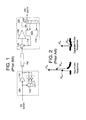
Figure 1 illustrates a prior-art signaling system having an equalizingoutput driver 109 and an equalizingreceiver 103 to mitigate dispersion-type ISI resulting from signal transmission on asignaling path 102. Thereceiver 103 includes asampling circuit 105 to generatedigitized samples 106 of the incoming signal, a shift register 107 to store some number (N) of the most recently received samples, and anequalizer 112 to generate anequalization signal 114 based on samples stored in the shift register 107. Ideally, theequalization signal 114 represents the residual signal level onpath 102 of the N prior received samples in the incoming signal so that, by subtracting theequalization signal 114 from the incoming signal indifference circuit 115, the dispersion-type ISI resulting from the prior transmission is canceled. Because the prior decisions of thesampling circuit 105 are fed back to the sampling circuit input in the form of theequalization signal 114, thereceiver 103 is commonly referred to as a decision feedback equalizer (DFE). - One major limitation of the DFE 103 is that the time delay in the overall feedback path from
sampling circuit 105 todifference circuit 115 makes it difficult to generate theequalization feedback signal 114 in time to equalize the signal level of the immediately following data value if the least latent sample (i.e., the most recently captured sample 106) is included in theequalization feedback signal 114. Including the least latent sample in the equalization signal is particularly challenging in modem high-speed signaling systems in which incoming symbols are present on thesignal path 102 for extremely brief intervals (e.g., less than a nanosecond for signal rates above one Gigabit per second). One solution to the least-latent sample problem is to omit one or more of the least-latent samples from contributing to generation of the decision-feedback equalization signal. Unfortunately, the least latent sample, being nearest in time to the incoming symbol, tends to be the largest contributor to dispersion-type ISI and therefore a primary objective of cancellation by the DFE. Consequently, in signaling systems in which the least-latent sample is omitted from contribution to decision-feedback equalization, transmit-side pre-emphasis is often used to decrease the dispersion-type ISI caused by the least-latent symbol. That is, when a given symbol is transmitted by the equalizingoutput driver 109, one or more previously transmitted symbols stored in shift register 113 (i.e., the least latent symbols relative to the outgoing symbol) are used to pre-shape the outgoing waveform to reduce the dispersion-type ISI observed at the receiver. Unfortunately, as can be seen in the raw and equalized pulse responses depicted inFigure 2 , forcing the least-latent sample, DN-1, to zero (or near zero) results in significant attenuation of the overall signal level, thereby reducing signaling margins and ultimately limiting the data rate of the signaling system. - The present invention is illustrated by way of example, and not by way of limitation, in the figures of the accompanying drawings and in which like reference numerals refer to similar elements and in which:
-
Figure 1 illustrates a prior-art signaling system; -
Figure 2 illustrates raw and equalized pulse responses observed in the prior art signaling system ofFigure 1 ; -
Figure 3 illustrates a signaling system that includes a partial response receiver according to an embodiment of the invention; -
Figure 4 illustrates a relationship between clock and data signals in one embodiment of the signaling system ofFigure 3 ; -
Figure 5 illustrates the bimodal distribution of a binary signal observed at a signal receiver when the primary source of dispersion-type ISI is the signal transmitted in the immediately preceding symbol time; -
Figure 6 illustrates the four partial response signal levels depicted inFigure 5 relative to a common mode level, LCM; -
Figure 7 illustrates a partial response receive circuit according to an embodiment of the invention; -
Figure 8 illustrates a double data rate signaling protocol in which two symbols are transmitted in succession during each cycle of a sampling clock signal; -
Figure 9 illustrates a partial response receive circuit for use in a double data rate signaling system; -
Figure 10 illustrates even and odd pipelines of sample values generated within the partial response receive circuit ofFigure 9 ; -
Figure 11 illustrates the use of embedded scoping to generate a time-based trace of an incoming data signal; -
Figure 12 illustrates a signaling system according to an embodiment of the invention; -
Figure 13 illustrates a waveform trace of a pulse response captured by an embedded scope within the signaling system ofFigure 12 ; -
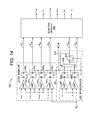
Figure 14 illustrates a partial response receiver according to an embodiment of the invention that adaptively generates partial response threshold levels; -
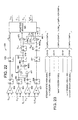
Figure 15 illustrates a embodiment of the adaptive module ofFigure 14 ; -
Figure 16 illustrates an alternative circuit arrangement that may be used in place of the averaging circuits ofFigure 15 ; -
Figure 17 illustrates a comparator that may be used within the receiver circuits and level sampling circuits ofFigures 7 ,9 and14 ; -
Figure 18 illustrates an embodiment of the current DAC ofFigure 17 ; -
Figure 19 illustrates an alternative comparator embodiment that may be used within the receiver circuits and level sampling circuits ofFigures 7 ,9 and14 ; -
Figure 20 illustrates a partial response receiver according to another alternative embodiment of the invention; -
Figure 21 illustrates the operation of the adaptive module ofFigure 20 according an embodiment of the invention; -
Figure 22 illustrates an embodiment of a dual mode receiver that may be operated in either a multi-level signaling mode or a partial response mode; -
Figure 23 illustrates a multi-level signaling protocol used within dual mode receiver ofFigure 22 ; -
Figure 24 illustrates a partial response receiver having a clock data recovery function according to an embodiment of the invention; -
Figure 25 illustrates a number of possible data signal transitions when the incoming data signal has the bimodal distribution shown inFigure 5 ; -
Figure 26 illustrates an embodiment of a clock recovery circuit that adjusts the phase of edge clock signal and sampling clock signal based on selected transitions detected in the incoming data signal; -
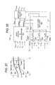
Figure 27 illustrates a potential source of non-convergence in a system that adaptively generates partial response threshold levels; -
Figure 28 illustrates an embodiment of a dual-mode, partial response receiver with clock data recovery; -
Figure 29 illustrates signal transitions between successive 4-PAM (Pulse Amplitude Modulation) symbols; -
Figure 30 illustrates data signal transitions that may be used for clock recovery when the dual mode receiver ofFigure 28 is operated in a partial response mode; -
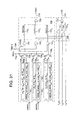
Figure 31 illustrates a transition detect circuit and sample select circuit that may be used within the clock recovery circuit ofFigure 28 ; -
Figure 32 illustrates additional data signal transitions that may be used for clock recovery when the dual mode receiver ofFigure 28 is operated in a partial response mode; -
Figure 33 illustrates a threshold select circuit according to an embodiment of the invention; -
Figure 34 illustrates a distribution of signal levels in a system in which the two most recently received symbols are the primary source of residual channel response; -
Figure 35 illustrates a partial response receiver according to an embodiment of the invention that operates in accordance with the partial response states shown inFigure 34 ; -
Figure 36 illustrates a partial response receiver according to another embodiment of the invention; -
Figure 37 illustrates a constellation of possible signal levels in a 4-PAM signaling system; -
Figure 38 illustrates a 4-PAM partial response receiver according to an embodiment of the invention; -
Figure 39 illustrates an input circuit that includes multiple partial response receivers according to an embodiment of the invention; -
Figure 40 illustrates an input circuit according to an alternative embodiment of the invention; -
Figure 41 illustrates a partial-response signaling system according to an embodiment of the invention; -
Figure 42 illustrates a raw pulse response and a pulse response equalized by the signaling system ofFigure 41 to enable partial-response data reception; and -
Figure 43 illustrates residual inter-symbol interference that may be equalized by transmit preemphasis within the signaling system ofFigure 41 . - In the following description and in the accompanying drawings, specific terminology and drawing symbols are set forth to provide a thorough understanding of the present invention. In some instances, the terminology and symbols may imply specific details that are not required to practice the invention. For example, the interconnection between circuit elements or circuit blocks may be shown or described as multi-conductor or single conductor signal lines. Each of the multi-conductor signal lines may alternatively be single-conductor signal lines, and each of the single-conductor signal lines may alternatively be multi-conductor signal lines. Signals and signaling paths shown or described as being single-ended may also be differential, and vice-versa. Similarly, signals described or depicted as having active-high or active-low logic levels may have opposite logic levels in alternative embodiments. As another example, circuits described or depicted as including metal oxide semiconductor (MOS) transistors may alternatively be implemented using bipolar technology or any other technology in which a signal-controlled current flow may be achieved. With respect to terminology, a signal is said to be "asserted" when the signal is driven to a low or high logic state (or charged to a high logic state or discharged to a low logic state) to indicate a particular condition. Conversely, a signal is said to be "deasserted" to indicate that the signal is driven (or charged or discharged) to a state other than the asserted state (including a high or low logic state, or the floating state that may occur when the signal driving circuit is transitioned to a high impedance condition, such as an open drain or open collector condition). A signal driving circuit is said to "output" a signal to a signal receiving circuit when the signal driving circuit asserts (or deasserts, if explicitly stated or indicated by context) the signal on a signal line coupled between the signal driving and signal receiving circuits. A signal line is said to be "activated" when a signal is asserted on the signal line, and "deactivated" when the signal is deasserted. Additionally, the prefix symbol "/" attached to signal names indicates that the signal is an active low signal (i.e., the asserted state is a logic low state). A line over a signal name (e.g., '
< signal name> ') is also used to indicate an active low signal. - A novel signal receiving circuit for use in electrical signaling systems is disclosed in various embodiments. In one embodiment, the signal receiving circuit includes a pair of comparators for comparing an incoming electrical signal against respective threshold levels, with each threshold level being set according to the level of a dispersed component of a previously received signal. More specifically, one of the threshold levels corresponds to the dispersion-type ISI introduced by a previously transmitted signal representative of a first digital state, and the other of the threshold levels corresponds to the dispersion-type ISI introduced when the previously transmitted signal is representative of a second digital state. In the case of a binary signaling system, the previously transmitted signal is resolved into one of two states by the receiving circuit, then used to select which of the comparators is to source the sample to be used for selection of the subsequent pair of samples. By this arrangement, each of the comparators compares the incoming signal against a threshold that is offset from a nominal value according to a respective, anticipated level of ISI, with the comparator having its threshold level offset in the direction that corresponds to the state of the previously received signal ultimately being selected as the sample source. Because samples are captured on the assumption of dispersion-type ISI resulting from both possible states of the previously captured sample (i.e., the least-latent sample), both samples are available for later selection when the state of the previously captured sample is resolved. Thus, by establishing separate threshold levels according to the different possible levels of dispersion-type ISI and comparing the incoming signal against each threshold level, the timing problems associated with generating an equalization signal that includes the least latent sample are avoided. Because the threshold level supplied to each of the comparators includes an offset according to the residual, partial response of the signaling path to the previously transmitted signal, a receive circuit having such offset-threshold comparators is referred to herein as a partial response receiver.
- In another embodiment of the invention, a multi-level signal receiver (i.e., receiver capable of receiving a symbol representative of more than a single binary bit), may be switched to a binary signaling, partial response mode. In one implementation, a multi-PAM receiver (Pulse Amplitude Modulation receiver -- a type of multi-level signal receiver) includes multiple comparators for distinguishing different possible levels (e.g., 4 levels in a 4-PAM receiver, 8 levels in an 8-PAM receiver, etc.) such that no additional comparators are necessary to support partial response operation. Instead, when the partial response mode is enabled, the threshold levels supplied to the comparators are adjusted to match the partial response levels for the least-latent symbol (or set of N least-latent symbols) and the post processing of the comparator outputs is switched from a symbol decoding operation to a sample selection operation.
- In other embodiments of the invention, methods and circuits for generating partial response threshold levels are disclosed. Also, methods and circuits for transmitting a partial-response data signal that includes a partial response from selected prior-transmitted bits are disclosed. Further, methods and circuits for recovering a clock signal from a partial response data signal are also disclosed.
-
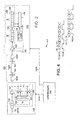
Figure 3 illustrates asignaling system 117 in which embodiments of the present invention may be used. Thesystem 117 includes an equalizingtransmitter 118 and equalizingreceiver 116 coupled to one another via a high-speed signal path 122, and acontroller 141 coupled to thetransmitter 118 and thereceiver 116 via relatively low-speed signal paths signal path 122 is formed bycomponent signal paths signal path 122B is formed on a backplane andsignal paths transmitter 118 andreceiver 116 are implemented in respective integrated circuit (IC) devices that are mounted on the daughterboards. The controller, which may be a general or special purpose processor, state machine or other logic circuit, is implemented within a third integrated circuit device mounted to a yet another circuit board. In the embodiment ofFigure 3 ,signal paths controller 141 to thetransmitter 118 andreceiver 116, respectively, and may be disposed on the same circuit board (or circuit boards) assignal path 122 or implemented by an alternative structure such as a cable. The controller may alternatively be coupled to thetransmitter 118 andreceiver 116 by a shared signal path such as a multi-drop bus. The operation of thecontroller 141 is discussed in greater detail below. In alternative embodiments, the IC devices containing thetransmitter 118,receiver 116 andcontroller 141 may be mounted to a common structure with the signalingpaths signal paths 122 and 142 formed between the ICs by bond wires or other conducting structures). Also, thetransmitter 118,receiver 116 andcontroller 141, or any subset thereof, may be included within the same IC device (e.g., system on chip) and the signalingpaths 122 and/or 142 implemented by a metal layer or other conducting structure within the IC device. - The equalizing
transmitter 118 transmits data on thesignaling path 122 during successive time intervals, referred to herein as symbol times. In one embodiment, illustrated by the timing diagram ofFigure 4 , each symbol time, TS, corresponds to a half cycle of a transmit clock signal, TCLK, such that two data values (e.g., values A and B) are transmitted on signalingpath 122 per transmit clock cycle. The transmitted data signal arrives at the input of the equalizingreceiver 116 after propagation time, TP, and is sampled by thereceiver 116 in response to edges of a receive clock signal, RCLK. The receive clock signal may be received within the receive circuit via an external clock line, or may be a recovered version of a reference clock signal (e.g., recovered by a delay-locked loop or phase locked loop circuit). In other embodiments, discussed below, the receive clock signal may be recovered from the transmitted data signal. Still referring toFigure 4 , the receive clock signal has a quadrature phase relation to data valid windows (i.e., data eyes) in the incoming data signal such that each sample is captured at the midpoint of a data eye. In alternative embodiments, the sampling instant may be skewed relative to data eye midpoints as necessary to satisfy signal setup and hold time requirements in thereceiver 116. Also, more or fewer symbols may be transmitted per cycle of the transmit clock signal. - The equalizing
transmitter 118 includes a transmitshift register 124,output driver 121 and transmitequalizer 129; the transmitequalizer 129 itself including ashift register 120 and a bank ofoutput drivers 131. At the start of each symbol time, the data value at the head (i.e., output) of the transmitshift register 124, referred to herein as the primary data value, is driven onto thesignal path 122 by theoutput driver 121, and the transmitequalizer 129 simultaneously drives an equalizing signal onto thesignal path 122. This type of equalization is referred to herein as transmit preemphasis. In one embodiment, the signal driven onto thesignal path 122 by the output driver 121 (referred to herein as the primary signal) is a multi-level signal having one of four possible states (e.g., defined by four distinct signal ranges) and therefore constitutes a symbol representative of two binary bits of information. In alternative embodiments, the primary signal may have more or fewer possible states and therefore represent more or fewer than two binary bits. Also, the primary signal may be single-ended or differential (an additional signal line is provided to carry the complement signal in the differential case), and may be a voltage or current mode signal. - Each of the
output drivers 131 within the transmitequalizer 129 form either a pre-tap driver or post-tap driver according to whether the source data value has already been transmitted (post-tap data) or is yet to be transmitted (pre-tap data). In the specific embodiment ofFigure 3 , the equalizer includes N post-tap drivers sourced by data values within theshift register 120 and one pre-tap driver sourced by a data value within the transmitshift register 124. Accordingly, the resultant equalizing signal driven onto thedata path 122 will have a signal level according to data values having symbol latencies of -1, 1, 2, ..., N, where the symbol latency of a given data value refers to the number of symbol times by which transmission of the data value precedes the transmission of the primary value. Different numbers of post-tap and pre-tap drivers may be provided in alternative embodiments, thereby allowing for equalization based on values having different symbol latencies. - Still referring to
Figure 3 , the equalizingreceiver 116 includes a partial-response receivecircuit 123, buffer 132 (e.g., shift register), tapselect circuit 128 and tapselect logic 139. Data signals are sampled by the partial response receivecircuit 123 to generate digitized samples that are stored in thebuffer 132 for eventual use by application logic (not shown). Because the buffered data is stored for at least a predetermined time and represents historical data up to a predetermined number of symbol latencies, the buffered data forms a source of post-tap data values that may be selected by the tapselect circuit 128 to source equalizer taps in a receive-side equalizer circuit. Because a subset of buffered data values may be selected according to the precise symbol latencies of reflections and other high-latency distortions, a relatively small number of buffered data values may be selected to form receive-side equalization taps having latencies that match the latencies of the distortions. By this arrangement, high latency distortions may be reduced by receive-side equalization without dramatically increasing the parasitic capacitance of the receiver (i.e., as would result from a large number of receive-side equalization taps). In one embodiment, the tapselect logic 139 is a configuration circuit that outputs a tapselect signal 134 according to a configuration value. The configuration value may be automatically generated by system 117 (e.g., at system startup) or may be empirically determined and stored within the configuration circuit or elsewhere withinsystem 117. - In the embodiment of
Figure 3 ,buffer 132 is formed by a shift register having adead range component 133 having M storage elements and a selectable-range component 135 having R storage elements, the tapselect circuit 128 being coupled to the selectable-range component 135 to select the subset of tap data sources therefrom. In alternative embodiments, the dead range component of thebuffer 132 may include fewer than M storage elements or even zero storage elements, depending on the time required to receive data and transfer data into thebuffer 132. Also, the tapselect circuit 128 may be coupled to one or more storage elements within thedead range component 133 to enable the size of the dead range to be programmed according to the configuration of the transmitcircuit 118. Finally, as discussed below, thebuffer 132 may include one or more parallel registers in addition to (or instead of) the shift register formed bycomponents - Still referring to
Figure 3 , numerous alternative types of equalization circuits may be used within thereceiver 116. For example, in one embodiment, thereceiver 116 includes an output driver 140 (illustrated in dashed outline inFigure 3 to indicate its optional nature) to drive an equalizing signal onto the signal path 122 (and therefore to the input of the partial response receive circuit 123) coincidentally with the symbol time of an incoming signal. In another embodiment, the partial response receivecircuit 123 includes a preamplifier having an equalizing subcircuit. -
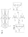
Figure 5 illustrates the bimodal distribution of a binary signal observed at a signal receiver when the primary source of dispersion-type ISI is the signal transmitted in the immediately preceding symbol time. That is, the symbol sampled at time TN-1 is the primary source of dispersion-type ISI in the symbol sampled at time TN; the symbol sampled at time TN is the primary source of dispersion-type ISI in the symbol sampled at time TN+1; and so forth. Referring to the signal levels at time TN, it can be seen that if the preceding symbol was a logic '1', the partial response to the preceding symbol will raise the signal level at time TN to one of the circled levels '11' or '01' (the second bit of the '11' and '01' bit sequences corresponding to the state of the signal at time TN-1). If the preceding symbol was a logic '0', the partial response to the preceding symbol will lower the signal level at time TN to one of the square-designated levels '10' or '00'. In a single-ended signaling system, the incoming signal is sampled and compared with a reference voltage level at the midpoint between the steady state extremes (i.e., midway between the '11..1' and '00..0' signal levels). Accordingly, the worst case voltage margins (i.e., smallest voltage differences between the signal and reference voltage) occur when the signal transitions from a '1' to a '0' or vice-versa; the '10' and '01' signaling levels becoming indistinguishable when the partial response level (i.e., residual signal level from the preceding symbol transmission) is large. In a differential signaling system, the incoming signal and its complement are sampled, for example, by a differential amplifier which amplifies the difference between the complementary signal levels. As in the single-ended case, the worst case voltage margins occur when the differential signal transitions from a '1' to a '0' or vice-versa; the '10' and '01' signaling levels becoming indistinguishable when the partial response pushes the '10' and '01' levels to the common mode (i.e., the average of a differential signal pair). -
Figure 6 illustrates the four partial response signal levels depicted inFigure 5 relative to a common mode level, LCM. In the case of a differential signaling system, the partial response to the preceding symbol may be viewed as increasing or decreasing the differential amplitude (i.e., the amplitude difference between the signals that form the differential signal pair) relative to a nominal differential amplitude. Normalizing the positive and negative signal levels for the nominal differential amplitude to 1 and -1, respectively, the common mode level, LCM, becomes zero, and the four possible signal levels become 1+α, 1-a, -1+α and -1-α, where α represents the magnitude of the partial response to the preceding symbol. Thus, when the preceding symbol, DN-1, is a '0', the incoming symbol, DN, is represented by a signal level at either 1-α or -1-α, depending on whether DN is a '1' or '0' Similarly, when DN-1= 1, the incoming symbol is represented by a signal level at either 1+α or -1+α according to the state of the current symbol. In the former case (i.e., when DN-1=0), the two complementary signal levels, -1-α and 1-α, have a common mode of -α, as shown inbox 151. In the latter case (i.e., when DN-1=1), the two complementary signal levels, 1+α and -1+α, have a common mode of +α, as shown inbox 153. -
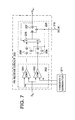
Figure 7 illustrates a partial response receivecircuit 200 according to an embodiment of the invention that exploits the bi-modal characteristic of the signal levels depicted inFigures 5 and 6 . Thepartial response circuit 200 includes a comparecircuit 202 to sample the input data signal, DN, and adecision circuit 204 to generate an output data value (i.e., received data value) based on data samples generated by the comparecircuit 202. Rather than a single comparator that distinguishes between binary signaling levels based on whether the sampled signal is above or below a common mode threshold, the comparecircuit 202 includes twocomparators comparator 201 is set the +α level, and the threshold level of thecomparator 203 is set to the -α level. By this arrangement, if the preceding symbol was a '1' (i.e., DN-1=1), thecomparator 201 will resolve the incoming signal as being a '1' or '0' by determining whether the signal level is above or below the partial response level, +α. Conversely, if DN-1=0, thecomparator 203 will resolve the incoming signal as being a '1' or '0' by determining whether the signal is above or below the partial response level, -α. Because both comparisons are performed for each incoming symbol, the selection of which comparator output represents the state of the symbol may be delayed until the state of the preceding symbol is resolved. In the partial response receivecircuit 200, for example, the sample values output by thecomparators decision circuit 204 where they are optionally stored instorage elements 208 and 209 (e.g., D flip-flops or other types of storage circuits) and provided to respective input ports of a select circuit 205 (e.g., a multiplexer). The sample value selected by theselect circuit 205 is stored in astorage circuit 207 in response to a sampling clock signal 210 (or other timing control signal) at which point the sample value becomes the DN-1 sample value. The DN-1 sample value stored withinstorage circuit 207 is fed back to the select input of theselect circuit 205 to select one of the two sample values generated by thecomparators select circuit 205, which of thecomparators storage elements storage circuit 207 becomes the DN-2 sample value and is used to select one of the DN-1 sample values output from thestorage elements - Reflecting on the operation of the partial response receive
circuit 200 ofFigure 7 in reference to the signal distribution shown inFigure 6 , it can be seen that the signaling margin (i.e., difference between signal levels representative of '1' and '0' states) within either of thecomparators circuit 200 ofFigure 7 remains substantially constant at 2, even as α grows. In effect, by offsetting the threshold of thecomparators - Still referring to
Figure 7 , athreshold generator 211 is used to generate the ±α thresholds supplied to thecomparators comparators Figure 6 . The threshold values ±α may also be digital values for controlling digital-to-analog converters (DACs) within thecomparators threshold generator 211 includes circuitry for a one-time or periodic determination of the ±α threshold levels, for example in one or more calibration operations. In other embodiments, the ±α threshold levels are adaptively generated based on incoming signal levels produced by selected data patterns. Embodiments of thethreshold generator 211 are discussed in further detail below. - In the partial response receive
circuit 200 ofFigure 7 , a single symbol is captured during each cycle of thesampling clock signal 210. That is, a rising (or falling) edge of the sample clock is used to capture samples of the incoming data signal. In a multi-data rate system, multiple symbols are captured per cycle of thesampling clock signal 210. In such systems, clock generation circuitry is provided to generate multiple instances of thesampling clock signal 210 that are phase-distributed through a period (1/frequency) of the sampling clock signal.Figure 8 , for example, depicts a double data rate signaling protocol in which two symbols are transmitted in succession during each period (i.e., cycle time) of a sampling clock signal. Accordingly, two instances of the sampling clock signal are provided: an even-phase sampling clock signal, SCLKE, to sample even-numbered symbols DN, DN+2, DN+4...; and an odd-phase sampling clock signal, SCLKO, to sample odd-numbered symbols DN-1, DN+1, DN+3... This technique may be extended to achieve virtually any data rate, including quad data rate (4 symbols per sampling clock cycle), octal data rate (8 symbols per sampling clock cycle), decade data rate (10 symbols per sampling clock cycle), and so forth. -
Figure 9 illustrates a partial response receivecircuit 215 for use in a double data rate signaling system. The partial response receivecircuit 215 includes an odd-phase receivecircuit 216 clocked by an odd-phase sampling clock signal 210O (SCLKO), and an even-phase receivecircuit 217 clocked by an even-phase sampling clock signal 210E (SCLKE). The odd- and even-phase receivecircuits circuit 200 ofFigure 7 , except that, due to the interleaved nature of the samples they generate, theselect circuit 225 of the odd-phase receivecircuit 216 is controlled by a latched instance of a sample selected by theselect circuit 239 in the even-phase receivecircuit 217 and, conversely, theselect circuit 239 of the even-phase receivecircuit 217 is controlled by a latched instance of a sample selected by theselect circuit 225 in the odd-phase receivecircuit 216. Samples DN +/DN - are generated bycomparators storage circuits 235 and 237, and then selected byselect circuit 239 to form the even-phase pipeline (EVEN PIPE) illustrated inFigure 10 (the output of theselect circuit 239 optionally being buffered instorage circuit 243 in response to the even-phase sampling clock signal 210E). Similarly, samples DN+1 +/DN+1 - are generated bycomparators storage circuits select circuit 225 form the odd-phase pipeline (ODD PIPE) illustrated inFigure 10 (the output of theselect circuit 225 optionally being buffered instorage circuit 227 in response to the odd-phase sampling clock signal 210O). Thus, when an odd phase sample DN-1 is selected byselect circuit 225, the DN-1 sample is latched withinlatch element 241 of the even-phase receive circuit (thereby making DN-1 available for a full cycle of the even-phase clock signal 210E) and thereafter used to select the subsequent even-phase sample DN. The selected even phase sample DN is then latched withinlatch element 228 of the odd-phase receiver and thereafter used to select the subsequent odd-phase sample, DN+1. For higher data rates, the number of partial-cycle receive circuits (circuits Figures 8-10 to support multi-data rate signaling. - In one embodiment of the invention, a technique referred to herein as embedded scoping is used to determine the ±α threshold levels applied within the comparators of the partial response receive circuit. Embedded scoping involves iteratively receiving a sequence of symbols in a receiver and comparing the received symbol sequence with a local generation of the sequence to confirm error-free reception. With each receive-and-confirm iteration, a threshold voltage used to distinguish between symbol values in the incoming signal is offset from a calibrated level by a progressively larger amount until a symbol in the sequence no longer matches the expected value. The threshold voltage offset at which the failure occurs is referred to herein as a pass/fail offset and represents a measure of the signal level at the sampling instant at which the failure occurred. Thus, by sweeping the threshold voltage through a range of threshold voltages until the pass/fail offsets for each symbol in the symbol sequence have been detected, a sample plot for the incoming signal may be developed. Further, by sweeping the receive clock signal through an incremental sequence of phase offsets, and determining the pass/fail offset at each phase offset, a complete trace of the incoming signal may be generated. Also, the granularity and start stop points of the phase offsets and/or threshold voltage steps may be controlled (e.g., by configuring a programmable circuit or register) to enable the waveform trace to be constrained to selected points of interest in the incoming signal (e.g., ±N° from an intended sampling instant, N representing a sweep angle).
-
Figure 11 illustrates the use of embedded scoping to generate a time-basedtrace 290 of an incoming data signal 286. The range of threshold voltage offsets over which theincoming signal 286 is sampled is indicated by VT, and the range of phase offsets at which the signal is sampled is indicated by φ. Each sample point within the sweep is indicated by a respective dot within a grid of sample points 280. Note that the sweep may be obtained by stepping the voltage threshold through the range of VT values for each value of φ, or, alternatively, by stepping the clock phase through the range of φ values for each value of VT. - Still referring to
Figure 11 ,reference numeral 288 indicates a pair of samples for which a pass/fail condition is detected. A corresponding pass/fail offset (PFO) is determined according to the difference between the calibrated VT level (VT(CAL)) and the average of the VT offsets between the pass and fail samples, and recorded as a measure of the incoming signal. That is, the pass/fail offset may be used to establish a data point within thetrace 290 as shown. After sweeping through all the sample points within the grid 280 (which sweep may be repeated numerous times to obtain an average and to discard statistical outliers), a measure of the incoming signal is obtained as illustrated graphically by thetrace 290. - Embedded scoping has a number of benefits over traditional signal measurement techniques. First, because the technique is non-invasive (i.e., no probe contact), the electrical characteristics of the system under test are unaltered, thereby yielding potentially more accurate results. Also, the trace is generated from the perspective of the receive circuit itself, meaning that any non-ideal characteristics of the receive circuit are accounted for in the resulting signal trace information. Finally, because all components needed for embedded scoping may be included within a finished signaling system, embedded scoping may be used to perform numerous run-time analyses in addition to partial response measurement including, without limitation, determining the latency and amplitude of reflections and other distortions within the signaling system.
-
Figure 12 illustrates asignaling system 300 according to an embodiment of the invention. Thesignaling system 300 includes a transmitdevice 301 and receivedevice 309 that employ embedded scoping to determine partial response amplitudes. The transmitdevice 301 includes apattern generator 303,data selector 305, equalizingtransmitter 307 andapplication logic 302. Theapplication logic 302 performs the core function of the transmitting device (e.g., signal processing, instruction processing, routing control or any other function) and provides transmit data (TX DATA) to a first input of thedata selector 305. During normal operation, theapplication logic 302 outputs a logic low scope signal 306 (SCOPE) to thedata selector 305 to select the transmit data to be passed to the equalizingtransmitter 307 for transmission to the receivedevice 309 via signal path 122 (which may include or be connected to numerous sources of discontinuity such as connectors, vias, stubs, etc.). During a scoping mode of operation, theapplication logic 302 drives thescope signal 306 high to enable a scoping mode of operation within the transmitdevice 301. In the scoping mode, thedata selector 305 selects a repeating single-symbol pulse sequence (e.g., a test signal such as: 00100...00100...00100...) generated by thepattern generator 303 to be transmitted to the receivedevice 309. The receivedevice 309 includes apartial response receiver 310 to receive the incoming data signal, apattern register 311 to store a local version of the single-symbol pulse sequence, amultiplexer 312 to enable the pattern register 311 to be switched between load and barrel-shifting modes, aXOR gate 313 to compare the received data sequence with the locally generated sequence, and application logic 315 (or other logic) to generate a threshold voltage adjust signal (THRESH ADJ) to step the threshold voltage used within the partial response receive circuit through their scoping ranges. In on embodiment, the thresholds applied to the multiple comparators of the partial response receive circuit are set to the same nominal starting value and stepped together for purposes of embedded scoping. In an alternative embodiment, only one comparator of the partial response receive circuit is used when scoping mode is enabled. The application logic may additionally generate a clock adjust signal (not shown) to step the sampling clock through a sequence of phase offsets within a cycle of the sampling clock signal. Theapplication logic 315 additionally builds a trace record (i.e., data indicative of the incoming data sequence) based on the output ofXOR gate 313. - When the receive
device 309 is in a scoping mode of operation, themultiplexer 312 is initially set to load the pattern register 311 with the output of thepartial response receiver 310. After a desired sequence of data (e.g., the single-symbol pulse sequence) is shifted into the pattern register 311, themultiplexer 312 is set to enable the barrel-shifting mode of thepattern register 311. That is, themultiplexer 312 selects the output of the pattern register 311 to be fed back to the input of the pattern register 311 so that the contents of the pattern register 311 are continuously rotated through the pattern register 311 (i.e., a barrel shifting operation). By this arrangement, the data sequence loaded into the pattern register 311 is repeatedly output, bit by bit, to a first input of theXOR gate 313. The data sequence received by thepartial response receiver 310 is input to a second input of theXOR gate 313 so that the received data sequence is compared, bit by bit, with the data sequence stored within thepattern register 311. By selecting the length of the repeatedly transmitted data sequence to match the storage size of the pattern register 311, the pattern register contents are repeatedly compared with a newly received version of the same data sequence (i.e., putatively the same data sequence). Any reception error will result in a mismatch between the received value and the corresponding value within the pattern register and therefore, when compared byXOR gate 313, will result in an error signal being output from theXOR gate 313 to theapplication logic 315. Theapplication logic 315 may then record the adjusted threshold voltage (and optionally the clock phase offset) at which the error occurred as a signal level within the waveform trace. -
Figure 13 illustrates asample waveform trace 320 of a pulse response captured by an embedded scope within the signaling system ofFigure 12 . As shown, the waveform starts and ends at a steady-state low level which corresponds to the -1-α level discussed in reference toFigures 5 and 6 . A pulse (i.e., D=1) is received at time T3, and the partial response of the pulse is received at time T4. Due to the preceding zero-valued symbol, the signal level sampled at time T3 corresponds to the 1-α level. Similarly, due to the preceding one-valued symbol, the signal level sampled at time T4 corresponds to the -1+α level. The difference between the -1+α level and the -1-α level may be determined by theapplication logic 315 ofFigure 12 (or other circuitry) and used to determine ±α. That is, α =((-1+α)-(-1-α))/2. The normalized signal level, 1, may be used in certain clock recovery operations (discussed below) and may be determined from the pulse level and the steady-state low level (i.e., 1=((1-α)-(-1-α))/2). Once determined, the α level may be applied to the comparators of the partial response receive circuit to enable partial response operation. -
Figure 14 illustrates apartial response receiver 325 that includes circuitry for adaptively generating the partial response threshold levels ±α. Thepartial response receiver 325 includes a partial response receivecircuit 200, alevel sampler 327, and anadaptive module 329. The partial response receivecircuit 200 operates generally as described above in reference toFigure 7 to generate a pair of sample values based on comparisons (incomparators 201 and 203) of the incoming signal DN with offset thresholds ±α. The samples are stored instorage elements select circuit 205 selects one of the DN-1 + and DN-1 - samples to be the selected DN-1 sample based on the state of the DN-2 sample stored instorage circuit 207. As discussed above, in a multi-data rate system, the DN-2 sample may be supplied by a counterpart partial response receive circuit clocked by a phase shifted version of thesampling clock signal 210. In either case, single- or multi-data rate, two or more time-adjacent sample values are supplied to (or buffered within) theadaptive module 329. In the embodiment ofFigure 14 , sample values DN-2 and DN-1 are supplied to theadaptive module 329, though higher or lower latency samples may be provided in alternative embodiments. - The
level sampler 327 includes four comparators 3311-3314 for comparing the signal level of the incoming symbol, DN, with each of the four signal levels that correspond to the bimodal signal distribution ofFigure 5 . That is,comparator 3314 compares the incoming signal with a threshold level at 1+α and generates a corresponding error sample E11 according to whether the incoming signal is above or below the 1+α level. Similarly,comparators adaptive module 329. By this arrangement, the error samples arrive at theadaptive module 329 with the same latency as the DN-1 sample generated by the partial response receivecircuit 200. - The
adaptive module 329 responds to the data samples from the partial response receivecircuit 200 and the error samples from thelevel sampler 327 by selectively updating the threshold values supplied to thecomparators circuit 200 and comparators 3311-3314 within thelevel sampler 327. For example, when the data samples indicate a 11 state (i.e., D[N-1:N-2]=11), theadaptive module 329 increases or decreases the 1+α threshold level according to whether the incoming signal level is indicated by error sample E11 to be above or below the 1+α threshold level. The adaptive module similarly updates the 1-α, -1+α, and -1-α thresholds based on error samples E10, E01 and E00 when the data samples indicate the 10, 01 and 00 states, respectively. As discussed below, the ±α levels may be derived from the 1+α, 1-α, -1+α and -1-α threshold levels, or a subset thereof. -
Figure 15 illustrates an embodiment of theadaptive module 329 ofFigure 14 . The adaptive module includes a 2:4decoder 353, up/down counters 3571-3574, averagingcircuits 361 and 365, digital-to-analog converters (DACs) 3591-3596, and, optionally, afilter circuit 351. The 2:4decoder 353 activates one of four enable signal lines 3541-3544 (i.e., asserts an enable signal on the signal line) according to the state of the input data samples DN-1 and DN-2 (also expressed herein as D[N-1:N-2]). Each of thecounters 357 has an up/down input (U/D) coupled to receive a respective one of the four error samples (i.e., E00, E01, E10 and E11), a count enable input (CEN) coupled to a respective one of theenable signal lines 354, and a strobe input coupled to receive thesample clock signal 210. By this arrangement, during each cycle of thesample clock signal 210, thecounter 357 coupled to the activated enablesignal line 354 is incremented or decremented according to the state of the corresponding error sample. Thus, when D[N-2:N-1] = 11,counter 3574 is incremented if error sample E11 indicates that the incoming signal level is above the 1+α threshold level, and decremented if E11 indicates that the incoming signal level is below the 1+α threshold level. The count values maintained withincounters signal lines 354. In one embodiment, thefilter circuit 351 is used to filter the incoming error samples, for example, by requiring a predetermined number of same-state error samples to be received within a given time before the corresponding count value is adjusted. Other types of error sample filtering may be applied in alternative embodiments. Also, thefilter 351 may be omitted altogether. - The count values maintained within the counters 3571-3574 are output as control values to respective DACs 3591-3594 to generate the 1+α, 1-α, -1+α and -1-α levels. Thus, the
adaptive module 329 operates to selectively update the 1+α, 1-α, -1+α and -1-α threshold levels according to the state of the received data values D[N-1:N-2]. - The averaging
circuits 361 and 365 generate the ±α threshold levels by averaging the control values output from counters 3571-3574. Averaging circuit 365, for example, includes a summingcircuit 366 to sum the C1+α and C-1+α control values fromcounters circuit 361 similarly includes a summingcircuit 362 to sum the count values C1-α and C-1-α fromcounters element 363 to generate control value C-α. In one embodiment, each of the control values generated by thecounters 357 and the averagingcircuits 361, 365 are input to respective DACs 3591-3596 to generate the threshold levels used within the comparators of the partial response receivecircuit 200 andlevel sampler 327 ofFigure 14 . In an alternative embodiment, each of the comparators within the partial response receivecircuit 200 andlevel sampler 327 include internal DACs and receive respective threshold values in the form of the control values themselves (i.e., Cα, C-α, C1+α, C1-α, C-1+α, C-1-α). Also, in a differential embodiment (and in certain single-ended embodiments), the C+α and C-α values may be complements of one another so that one of the averagingcircuits 361 or 365 may be replaced by a multi-bit inverter. Further, the C1+α and C-1-α values may be complements, and the C1-α and C-1+α values may be complements such that two of the comparators within thelevel sampler 327 ofFigure 14 and two of thecounters 357 within the adaptive module 329 (and two of theDACs 359, if used) may be omitted. -
Figure 16 illustrates analternative circuit arrangement 375 that may be used in place of the averagingcircuits 361 and 365 ofFigure 15 . Instead of averaging the C1+α and C-1+α count values to generate the C+α value, C+α is generated by halving the difference between the C1+α and the C1-α control values (i.e., Cα = ((C1+α)-(C1-α))/2). Similarly, the C-α value is generated by halving the difference between the C-1-α and the C-1+α control values. Thus, the circuit ofFigure 16 includes adifference circuit 376 to generate 2α by subtracting the C1-α control value from the C1+α control value, and a divide-by-2 element 377 (which may be a implemented by dropping the least significant bit of the difference) to generate Cα by halving the 2α value.Difference circuit 379 and divide-by-2element 380 are used in a similar manner to generate C-α from count values C-1+α and C-1-α in a corresponding manner. -
Figure 17 illustrates a comparator 400 that may be used within the receiver circuits and level sampling circuits ofFigures 7 ,9 and14 . The comparator 400 includes apreamplifier 401 and asampling circuit 425. Thepreamplifier 401 includes a pair ofdifferential amplifiers second output nodes Transistors differential amplifier 402 have widths W1 and W2, respectively, with W1 being greater than W2. Transistors 408 and 407 withindifferential amplifier 403 also have respective widths W1 and W2. A differential input signal composed of signal components D and /D is coupled to each of thedifferential amplifiers transistors 404 and 408 and /D is coupled totransistors 405 and 407. By this arrangement, when Cα and /Cα are substantially equal (e.g., in an 8-bit control word, Cα =128 and / Cα =127), thedifferential amplifiers transistors 404 and 408 will collectively sink more current thantransistors 405 and 407, thereby causing the voltage onoutput node 418 to be pulled down (i.e., via the resistive element, R, coupled to the output node 418) more than the voltage onoutput node 419. - When the
preamplifier 401 is balanced (i.e., Cα substantially equal to /Cα), the voltages on thepreamplifier output nodes preamplifier 401, and therefore the comparator 400 as a whole, occurs at the common mode of D and /D. By contrast, when the preamplifier is imbalanced by increasing Cα relative to /Cα, equal values of D and /D result inoutput node 419 being pulled lower thanoutput node 418, due to the fact thattransistor 405 is wider than transistor 404 (and therefore has a greater gain), and that the compensating (balancing) effect ofdifferential amplifier 403 is diminished by the reduced control value /Cα. Thus, increasing Cα relative to /Cα increases the effective threshold of the preamplifier above the common mode. By increasing Cα to the point at which the threshold between '0' and '1' signal levels is set to α, a differential comparator having a threshold level at α is achieved. By reversing the connections of the Cα and /Cα values to the current DACs of a counterpart comparator (not shown), a differential comparator having a threshold level at -α is achieved. - The
sampling circuit 425 includes adifferential amplifier 426 formed bytransistors sense amplifier 427 formed by back-to-back coupledinverters storage circuit 436 formed by a set-reset flip-flop. Thedifferential amplifier 426 includes control inputs coupled to theoutput nodes preamplifier 401, andoutput nodes inverters transistor 430, switchably controlled by the sampling clock signal 210 (or other sample control signal), is coupled between thedifferential amplifier 426 and a ground reference (or other low voltage reference). Thesampling clock signal 210 is additionally coupled to control inputs of positively-doped MOS (PMOS)transistors 434 and 435 which are coupled between a supply voltage (e.g., VDD) and output nodes of theinverters sample clock signal 210 is low,transistor 430 is switched off, andtransistors 434 and 435 are switched on to precharge the output nodes of theinverters inverters storage circuit 436, so that the content of thestorage circuit 436 is maintained through the low half-cycle of thesample clock signal 210. When thesample clock signal 210 goes high, biasingtransistor 430 is switched on and draws current through the twotransistors differential amplifier 426 in proportion to the voltages developed on theoutput nodes preamplifier 401. Thus, if the voltage developed onnode 419 is higher than the voltage onnode 418, the current drawn by biasingtransistor 430 will flow primarily throughtransistor 423. Conversely, if the voltage developed onnode 418 is higher than the voltage on 419, the current drawn by biasing transistor will flow primarily throughtransistor 423.Transistors 434 and 435 are switched off in response to the high-goingsample clock signal 210, so that the pre-charged outputs of theinverters transistors transistor 430 will flow primarily throughtransistor 423. Consequently, the output node ofinverter 429 will be discharged more rapidly than the output node ofinverter 428, driving the output ofinverter 429 low and driving the output ofinverter 428 high (i.e., the PMOS transistor withininverter 428 is switched on and the NMOS transistor withininverter 428 is switched off). The low output ofinverter 429 is applied to the active-low set input of thestorage circuit 436, causing thestorage circuit 436 to store a logic '1' sampled data value. By contrast, if the incoming signal level does not exceed the +α threshold level, the current drawn by biasingtransistor 430 will flow primarily throughtransistor 424, thereby drivinginverter 428 low (and drivinginverter 429 high) to store a logic '0' sampled data value withinstorage circuit 436. -
Figure 18 illustrates an embodiment of thecurrent DAC 411 ofFigure 17 . Thecurrent DAC 411 includes control transistors 4370-437N-1 and biasing transistors 4390-439N-1. Each of the control transistors 4370-437N-1 is coupled in series (e.g., source to drain) with a corresponding one of the biasing transistors 4390-439N-1 to form a transistor pair that is coupled between a reference voltage (ground in this example) and an output node 438 (i.e., the node to be connected to the source terminals of the transistors which form the differential amplifier 402). Gate terminals of the control transistors 4370-437N-1 are coupled to receive respective component signals, Cα [0] - Cα [N-1], of a multi-bit control value, Cα (or, control value /Cα). Each of the control transistors 4370-437N-1 has a binary weighted gain such that a current of IREFx 2i (where i represents the ith transistor in thepositions control transistor 437i when the corresponding control signal component is high. Thus, if all the constituent bits of the control value Cα [N-1:0] are high, then IREF flows throughcontrol transistor 4370, IREF x2 flows throughtransistor 4371, IREF x4 flows throughcontrol transistor 4372, and so forth to controltransistor 437N-1 which conducts IREF x2N-1. Accordingly, control transistors 4370-437N-1 are designated x1, x2..., x2N-1 transistors, respectively. By this arrangement, the control value Cα [N-1:0] may be set to any of 2N values to select bias currents that range from 0 to IREF x2N-1 in increments of IREF. The biasing transistors 4390-439N-1 have gate terminals coupled to receive a bias voltage, VBIAS, that is adjusted as necessary (e.g., by a biasing circuit) to establish or maintain a desired IREF. - In one embodiment, the relative gains (i.e., transconductance values) of the various transistors used to implement the current DAC 411 (and therefore drive strengths of the sub-drivers) are established by adjusting the width-length ratio (i.e., W/L) of
individual control transistors 437 and/or biasingtransistors 439. For example, the width-length ratio of thex2 control transistor 4371 is twice the width-length ratio of thex1 control transistor 4370, the width-length ratio of thex4 control transistor 4372 is twice the width-length ratio of thex2 control transistor 4371, and so forth. The biasingtransistors 439 may have similar gain ratios relative to one another (e.g., x1, x2, x4, x2N-1 as shown inFigure 18 ). Other techniques for adjusting the relative gains of thecontrol transistors 437 and biasingtransistors 439 may be used in alternative embodiments. Also, weightings other than binary weightings may be used. For example, in one embodiment, each of thecontrol transistors 437 has an equal gain to each of theother control transistors 437 such that the current drawn by thecurrent DAC 411 is proportional to the number of logic '1' bits in the control value, Cα. -
Figure 19 illustrates an alternative embodiment of adifferential comparator 450 that may be used to implement the comparators depicted inFigures 7 ,9 and14 . Thecomparator 450 includes asampling circuit 452 and an offsetcontrol circuit 440. Thesampling circuit 452 is implemented in generally the same manner as thesampling circuit 425 ofFigure 17 (and includesdifferential amplifier 426,sense amplifier 427, biasingtransistor 430, and storage circuit 436), except that the input signal lines carrying D and /D are coupled directly to the control terminals oftransistors control circuit 440 includes adifferential amplifier 446 having output nodes coupled tonodes sampling circuit 452. Control terminals of thetransistors differential amplifier 446 are biased by respective voltage DACs (e.g., implemented bycurrent DACs 443 and 445 coupled to respective resistive pull-upelements 451 and 453) controlled by Cα and /Cα, respectively. By this arrangement, when the sample clock signal goes high the current throughoutput node 433 of thesampling circuit 452 is a sum of the currents drawn bytransistor 423 of thesampling circuit 452 andtransistor 447 of the offsetcontrol circuit 440. Similarly, the current throughnode 431 of thesampling circuit 452 is a sum of the currents drawn bytransistor 424 of thesampling circuit 452 andtransistor 449 of the offsetcontrol circuit 440. As discussed above in reference toFigure 17 , when the current throughnode 431 exceeds the current throughnode 433, a logic '1' is stored withinstorage circuit 436 and, conversely, when the current throughnode 433 exceeds the current throughnode 431, a logic '0' is stored withinstorage circuit 436. - When the DAC control values Cα and /Cα are substantially the same, the
comparator 450 is balanced and the effective threshold occurs at the common mode of the D and /D signal levels. That is, if D exceeds the common mode voltage, VCM = ((D + /D) divided by 2), the current throughnode 433 exceeds the current throughnode 431, causing a logic '1' to be captured as the sampled data value. As Cα is increased and /Cα decreased, the effective threshold of the differential amplifier is increased such that D must be higher than /D by an amount necessary to overcome the additional current drawn bytransistor 449 of the offset control circuit. Thus, by increasing Cα and decreasing /Cα, the effective threshold of the sampling circuit may be set to the partial response level, α. That is, a logic '1' is output as the sampled data value if the difference between the D exceeds the common mode voltage, VCM by more than α, and a logic '0' is output otherwise. A counterpart comparator having a -α threshold may be provided by switching the Cα and /Cα inputs to theDACs 443 and 445. -
Figure 20 illustrates apartial response receiver 500 according to another alternative embodiment. Thepartial response receiver 500 includes a partial response receivecircuit 200 that operates generally as described in reference toFigures 7 and14 , alevel sampler 501, and anadaptive module 503. In contrast to thelevel sampler 327 ofFigure 14 , thelevel sampler 501 includes asingle comparator 507 that generates an error sample, EDLEV, according to whether the incoming signal exceeds or is below a data level threshold generated by theadaptive module 503. In the embodiment ofFigure 20 , the data level threshold is established by a multi-bit control value, CDLEV, generated by the adaptive module. In alternative embodiments, the data level threshold may be established by an analog voltage or current generated by theadaptive module 503. The error sample may be buffered in one ormore storage circuits 509 before being forwarded to theadaptive module 503, thereby aligning the latency of the error sample with data samples generated by the partial response receivecircuit 200. - The
adaptive module 503 receives the error sample from thelevel sampler 501 and data samples DN-1 and DN-2 from the partial response receivecircuit 200 and, in response, generates control values, Cα and /Cα, to establish the ±α levels within the partial response receivecircuit 200, and the control value, CDLEV, to establish the data level threshold within thelevel sampler 501. In one embodiment, theadaptive module 503 initially updates the CDLEV value upon detecting reception of the 1+α data pattern (i.e., D[N-1:N-2]=11) until thecomparator 507 indicates that the data level threshold matches the 1+α data level. Thereafter, theadaptive module 503 updates the CDLEV value in response to the 1-α data pattern (10) until the DLEV threshold matches the 1-α data level. The control value, Cα, may be generated, for example, by halving the difference between the two CDLEV values (i.e., C1+α and C1-α), and the /Cα control value may be generated by complementing the Cα value. -
Figure 21 illustrates the operation of theadaptive module 503 ofFigure 20 according one embodiment. Initially, atblock 521, the control values, Cα and CDLEV, and an internally maintained control value, C2α, are each set to a nominal zero value. In one embodiment, the nominal zero value corresponds to a DAC midpoint value. For example, in an 8-bit DAC, a midpoint value of 1000 0000b (the 'b' indicating binary notation) or 128 decimal may be used as the nominal zero value. The C-α value may be generated by subtracting the Cα value from the full-scale DAC value. Thus, in the eight-bit example, when C+α = 128, C-α = (28-1) - 128 = 127. It will be appreciated that this result may be obtained by complementing Cα (i.e., /Cα = C-α). - At
decision block 523, a history of increment and decrement operations applied to CDLEV value is evaluated to determine whether the threshold level that corresponds to the 1+α signal level has been reached (i.e., UPPER DLEV FOUND). In one embodiment, if, over the last N updates to the CDLEV value, the difference between the number of increment operations and the number of decrement operations is less than a predetermined value, the data level threshold is deemed to be dithering about the 1+α signal level and the upper data level threshold is therefore considered found. If the upper data level threshold has not been found, then the sample values generated by the partial response receive circuit (D[N-1:N-2]) are evaluated indecision block 525 to determine whether a signal level at the 1+α level has been received. If so, the error sample generated by the level sampler, EDLEV, is evaluated indecision block 527 to determine whether the incoming signal level is greater than or less than the threshold level established by the present value of CDLEV. If the error sample is a '1', the incoming signal level is greater than the threshold level, and the CDLEV value is incremented at 529 to increase the data level threshold. If the error sample is a '0', the signal level is less than the data level threshold and the CDLEV value is decremented at 531 to decrease the data level threshold. As discussed above in reference toFigure 15 , some level of filtering may be applied before incrementing or decrementing the CDLEV value. After the CDLEV value has been incremented or decremented (i.e., inblock 529 or 531), the CDLEV increment/decrement history is evaluated again atdecision block 523 to determine whether the upper data level threshold has been found. - Returning to decision block 525, if D[N-1:N-2] is not equal to '11', the error sample, EDLEV, is not evaluated and the operation at 525 is repeated for a subsequent set of data samples. Thus, in the level-adapting loop formed by blocks 523-531, the adaptive module selectively updates the CDLEV value, and therefore the data level threshold according to the state of the data samples generated by the partial response receive circuit (i.e., updates the CDLEV value in response to detection of the 1+α sample pattern).
- If, at
decision block 523, the upper data level is deemed to be found, the history of increment and decrement operations is cleared and a second level adapting loop is begun atdecision block 535. Atdecision block 535, the history of increment and decrement operations is evaluated to determine whether a data level threshold corresponding to the 1-α data level has been found (i.e., LOWER DLEV FOUND). In one embodiment, if, over the last N updates to the CDLEV value, the difference between the number of increment operations and the number of decrement operations is less than a predetermined value, the data level threshold is deemed to be dithering about the 1-α signal level and the lower data level threshold is therefore considered found. If the lower data level threshold has not been found, then the sample values generated by the partial response receive circuit, D[N-1:N-2], are evaluated indecision block 537 to determine whether a signal level at the 1-α level has been received. If not,decision block 537 is repeatedly entered for subsequent sample value pairs until a signal level at the 1-α level has been received. When data samples that correspond to the 1-α level are detected, the error sample generated by the level sampling circuit, EDLEV, is evaluated atdecision block 539 to determine whether the incoming signal level is above or below the data threshold level established by the present value of CDLEV. If the error sample is a '0', as it will be initially, the signal level is below the data threshold level, and the CDLEV value is decremented at 543 to decrease the DLEV threshold level, and the C2α control value is incremented to track the difference between the upper and lower data level thresholds. If the error sample is determined to be a '1' atdecision block 537, then CDLEV is incremented and C2α decremented atblock 541. By this arrangement, when the data level threshold reaches the 1-α data level, the control value, C2α, will be representative of twice the +α threshold level. Accordingly, atblock 545, the Cα value is generated by dividing C2α by 2 (e.g., by right shifting or otherwise dropping the least significant bit of C2α). The C-α value may be generated by complementing the Cα value. Thereafter, the process is repeated starting atdecision block 523. Alternatively, an updated C2α value may be generated by counting the return increments from the lower data level threshold to the upper data level threshold, and another updated value of C2α generated on a subsequent return to the lower data level threshold, and so forth. The Cα value may be updated after each regeneration of the C2α value. Also, rather than finding the 1+α and 1-α data levels, the 1+α and -1+α data levels may be determined, and the corresponding data level control values averaged to generate the Cα value. -
Figure 22 illustrates an embodiment of adual mode receiver 550 that may be operated in either a multi-level signaling mode or a partial response mode. When a mode select signal 572 (MSEL) is in a first state (e.g., a logic low state), a two-bit per symbol, multi-level signaling mode is selected. In one embodiment, illustrated inFigure 23 , the signal level of each incoming symbol falls into one of four voltage ranges distinguished by three threshold levels. The four voltage ranges are designated 10, 11, 01 and 00 inFigure 23 according to the pair of data bits represented at each level. Because each symbol constitutes a pulse having one of four possible amplitudes, the incoming multi-level signal is referred to herein as a 4-PAM (Pulse Amplitude Modulation) signal. Different PAM levels (e.g., 8-PAM, 10-PAM, etc.) may be used in alternative embodiments. - In the multi-level signaling mode,
comparator 557 compares the incoming signal with a midlevel threshold (referred to herein as the zero threshold) to determine the state of the most significant bit (MSB) of the symbol. In the embodiment ofFigures 22 and 23 , the MSB is resolved to be a '1' if the signal level exceeds the zero threshold, and a '0' if the signal level does not exceed the zero threshold.Comparators Figure 23 , if the incoming signal level exceeds the +α threshold level, bothcomparators comparators comparators comparators gate 561 is coupled to receive the sample values generated by thecomparators 553 and 555 (i.e., after the sample values are buffered instorage circuits 554 and 556), and outputs the LSB to a first port ofselect circuit 565. When the mode select signal selects the 4-PAM mode of the dual-mode receiver, the LSB is selected to be passed to nextstage storage circuits select circuit 579 to be provided to theadaptive module 581. Thus, in 4-PAM mode, theadaptive module 581 receives an LSB and MSB (the MSB bit being stored in succession instorage circuits comparators - It should be noted that the threshold levels and data signal levels described in reference to
Figure 23 may be used in both differential and single-ended signaling systems. In the case of single-ended signaling systems, the voltage levels of the thresholds and data signals are expressed as an offset from a common, substantially fixed reference voltage, such as a ground reference. In differential signaling systems, the data signals and thresholds are each represented by differential signal pair, with the voltage level of the data signal or threshold being the voltage difference between the two differential signals (e.g., subtracting the voltage level of one signal from the other). - Still referring to the 4-PAM mode of the
dual mode receiver 550, thecomparator 551 generates an error sample EDLEV that is buffered withinstorage circuits adaptive module 581. In one embodiment, the adaptive module generates the 4-PAM mode threshold level control values C0, C+α and C-α (i.e., the control values supplied tocomparators Figure 14 , the error sample generated by thecomparator 551 may be filtered to obtain thesteady state 11 signal level and thesteady state 00 signal level. - Still referring to
Figure 22 , when the modeselect signal 572 is high, thedual mode receiver 550 is switched to the partial response mode. In the partial response mode, thecomparators comparators storage circuits circuit 563 which selects one of the samples according to the state of the previously received sample. That is, one of the DN-1 samples stored instorage circuits storage circuit 567 according to the DN-2 sample previously stored in thestorage circuit 567. The DN-2 sample is stored in thestorage circuit 578 to generate the DN-3 sample value. During a given symbol time, both the DN-2 and DN-3 samples are provided to theadaptive module 581 viaselect circuits adaptive module 581 receives the MSB/LSB pair for each incoming 4-PAM symbol, and in partial response mode, theadaptive module 581 receives the D[N-2:N-3] sample values that represent one of the four states of the bimodal signal illustrated inFigure 5 . - Still referring to
Figure 22 , in partial response mode, thecomparator 551 andadaptive module 581 operate to generate the +α and - a levels in the manner described in reference toFigures 20 and21 . Alternatively, because theMSB comparator 557 is not otherwise used in the partial response mode, thecomparator 557 may be used to determine the level of the 1-α partial response state, thereby enabling both the 1+α and 1-α signal levels to be determined simultaneously. The ±α levels may then be generated based on the 1+α and the 1-α signal levels (i.e., Cα =((C1+α) - (C1-α))/2, and C-α = /Cα). In another alternative embodiment, the MSB comparator may be used to determine the -1+α signal level, thereby enabling ±α to be determined by averaging the 1+α and -1+α signal levels. The error signal generated by the MSB comparator, E10 (or E01) is illustrated by dashedline 574 to indicate its optional nature. - Reflecting on the
dual mode receiver 550 ofFigure 22 , it can be seen that much of the circuitry provided for 4-PAM operation (e.g., the four comparators (551, 553, 555 and 557), storage circuits (552, 554, 556, 558, 567, 570, 571, 578 and 573) and adaptive module 581) is re-used in the 2-PAM partial response mode, thereby providing partial response operation with relatively little additional hardware overhead. The modeselect signal 572 may be provided from an external source or from a configuration control circuit within the integrated device that includes thedual mode receiver 550. In one embodiment, the configuration control circuit is a configuration register that may be programmed by one or more other integrated circuits within a system (e.g., a host processor or similar control device) to establish the mode of thedual mode receiver 550. The configuration control circuit may also be a non-volatile control circuit such as a non-volatile memory, fusible circuit or similar circuit that may be programmed with a mode select value. In yet other embodiments, the configuration control circuit may dynamically change the state of the mode select signal in response to detecting selected system conditions (e.g., detection of threshold error rate when in one operating mode or the other). -
Figure 24 illustrates an embodiment of apartial response receiver 600 that performs a clock data recovery (CDR) function. That is, thepartial response receiver 600 recovers both data and clocking information from the incoming data signal, DN. Thepartial response receiver 600 includes a data receive andlevel sampling circuit 601,adaptive module 603,clock recovery circuit 605, edge-sampling comparator 607, and one ormore storage circuits 609. The data receive andlevel sampling circuit 601 operates as described above in reference toFigures 14 and20 to generate one or more error samples, EDLEV, and data samples D[N-1:N-2]. The data receive andlevel sampling circuit 601 may also be operable in a multi-PAM mode as described in reference toFigure 22 . Theadaptive module 603 generates one or more threshold control values that are supplied to the data receive andlevel sampling circuit 601, including one or more data level control values, CDLEV, and partial response control values, C+α and C-α. The control values are used to establish threshold values in the partial response compare circuits (i.e., the ±α comparators) and one or more level adapting comparators as discussed above. - The
clock recovery circuit 605 generates a sampling clock signal 210 (SCLK) and edge clock signal 610 (ECLK) in response to a transition sample, TN-1, generated by the edge-sampling comparator 607 and the data and error samples generated by the data receive and level sampling circuit 601 (i.e., EDLEV and D[N-1:N-2]). Thesampling clock signal 210 is used to time the operation of comparators and storage circuits within the data receive andlevel sampling circuit 601 and, at least in one embodiment, is phase aligned with midpoints in the incoming data eyes (i.e., midpoint of data valid intervals in the incoming data signal, DN). In an alternative embodiment, thesampling clock signal 210 may be offset from the midpoints in the incoming data eyes, for example, to accommodate asymmetric setup and hold time requirements in the comparators or other circuitry in the data receive andlevel sampling circuit 601. Note that while only a singlesampling clock signal 210 is shown, multiple sampling clocks may be generated by the clock recovery circuit to enable receipt of multi-data rate signals. For example, in a double data rate system, the clock recovery circuit may generate SCLK and /SCLK to enable capture of data and signal level samples in both odd and even phases of thesampling clock signal 210. - The
clock recovery circuit 605 adjusts the phase of theedge clock signal 610 to maintain phase alignment between theedge clock signal 610 and transition points between incoming data eyes (i.e., theedge clock signal 610 is edge aligned with data valid intervals in the incoming data signal). Theedge clock signal 610 is supplied to the edge-sampling comparator 607 where it is used to time the sampling of transitions in the incoming data signal, and to one ormore storage circuits 609 provided to latency-align the transition sample, TN-1, with the data sample, DN-1. In the case of a low-to-high data signal transition, a logic '1' transition sample (i.e., TN-1=1) indicates that the edge clock transition occurred after the transition in the data signal and therefore that theedge clock signal 610 lags the data signal transition. Conversely, a logic '0' transition sample indicates that the edge clock transition occurred prior to the low-to-high data signal transition and therefore that theedge clock signal 610 leads the data signal transition. The transition samples from edge-sampling comparator 607 and data samples from the data receive andlevel sampling circuit 601 are used within theclock recovery circuit 605 to adjust the phase of theedge clock signal 610 as necessary to maintain alignment between theedge clock signal 610 and transitions in the incoming data signal. In one embodiment, thesampling clock signal 210 is maintained at a substantially constant phase offset from theedge clock signal 610 such that phase alignment between theedge clock signal 610 and data signal transitions yields a desired phase alignment between thesampling clock signal 210 and midpoints in the incoming data eyes. -
Figure 25 illustrates a number of possible data signal transitions when the incoming data signal has the bimodal distribution shown inFigure 5 . That is, if the incoming data signal has one of the four bimodal signal levels corresponding to the partial response states 11, 10, 01, 00, then the signal may transition from either the 11 or 10 level to the 01 level (i.e., D[N-1:N-2]=11 or 10 and D[N:N-1]=01), and the signal may transition from either the 00 or 01 level to the 10 level. Note that signal transitions from the 10 level to the 11 level (illustrated by dashed line 631) and from the 01 level to the 00 level (illustrated by dashed line 632)are also possible. - Considering the transitions from 10-to-01 and from 01-to-10, it can be seen that each of these transitions crosses the midpoint threshold (i.e., zero threshold level) at a time, T1, midway between the centers of the
data eyes edge clock signal 610 is phase aligned to the transitions in the incoming data signal, the 10-to-01 and 01-to-10 data signal transitions cross the midpoint threshold coincidentally (i.e., in phase alignment) with the edge clock transition. Accordingly, the 10-to-01 and 01-to-10 transitions may be compared with the zero threshold level (designated '0' inFigure 25 ) to generate transition samples for adjusting the phase of the edge clock signal. Note that, because the signal swings in the transitions from 11-to-01 and 00-to-10 are not symmetric with respect to the zero threshold level, the 11-to-01 and 00-to-10 transitions do not cross the zero threshold level at the same time as the 10-to-01 and 01-to-10 transitions, but rather cross the zero threshold level at some time later (indicated by circle 636). Consequently, use of the 11-to-01 and 00-to-10 transitions to determine zero-crossing times (i.e., times at which the zero threshold level is crossed) may introduce phase error and/or bi-modal jitter in the recovered edge and sampling clock signals 610 and 210. Accordingly, in one embodiment of the invention, transitions in the incoming data signal are selected according to their zero-crossing characteristics, with the selected transitions being used to adjust the phase of the edge and sampling clock signals 610 and 210. -
Figure 26 illustrates an embodiment of aclock recovery circuit 650 that adjusts the phase ofedge clock signal 610 andsampling clock signal 210 based on selected transitions detected in the incoming data signal. Theclock recovery circuit 650 includes a transition detectcircuit 651, early/late detector 661, early/late counter 663,majority detector 665,interpolator 667 andreference loop 669. In the embodiment ofFigure 26 , the transition detectcircuit 651 asserts a transition detect signal 652 (TDET) upon detecting a 01-to-10 or a 10-to-01 transition in the incoming data signal. More specifically, incoming data samples DN-1 and DN-2 are compared in exclusive-OR gate 653 to determine whether a transition has occurred, and signals DN and DN-2 are compared in exclusive-NORgate 657 to determine whether the DN state matches the DN-2 state. The outputs of the exclusive OR and exclusive-NORgates signal 652. By this arrangement, the transition detectsignal 652 goes high if D[N:N-2] = 010 or 101 (i.e., in response to a 01-to-10 transition or a 10-to-01 transition). The transition detectsignal 652 is applied to a count enable input (CEN) of the early/late counter 663 to enable an early/late count value to be incremented or decremented according to the output of the early/late detector 661. In one embodiment, the earlylate detector 661 is implemented by an exclusive OR gate, and therefore asserts an early signal 654 (e.g., a logic high signal) if the transition sample, TN, does not match data sample DN, and a late signal (e.g., logic low signal 654) if the TN matches DN. That is, if the transition sample is captured after the transition from DN-1 to DN, the transition sample will match the DN sample and thereby indicate that the edge clock signal transition is late relative to the data signal transition. Conversely, if the transition sample is captured before the transition from DN-1 to DN, the transition sample will not match the DN sample and thereby indicate that the edge clock signal transition is early relative to the data signal transition. - In one embodiment, the early/
late counter 663 is initialized to a zero level, and is then incremented in response to an early signal (i.e., from the early/late detector 661) and decremented in response to a late signal. By this arrangement, the sign bit (e.g., the MSB) of the early/late count maintained within the early/late counter 663 indicates whether more early signals than late signals, or more late than early signals have been received from the early/late detector (i.e., the count value will underflow to a negative value if more late signals than early signals are detected). Accordingly, after a predetermined number of transition detect assertions (or after a predetermined time), themajority detector 665 evaluates the sign of the early/late count and asserts an up/downsignal 668 to the interpolator accordingly. The early/late count value may then be reset to zero in order to count a subsequent set of early/late signal assertions. - In one embodiment, the
interpolator 667 maintains a digital control word that is incremented in response to a logic high up/downsignal 668 and decremented in response to a logic low up/downsignal 668. The most significant bits of the digital control word are used to select a pair of phase vectors from the set ofN phase vectors 672 generated by thereference loop 669, and the least significant bits of the digital control word are used to interpolate between the selected pair of phase vectors. As the control word is incremented, the interpolation is incrementally shifted from a leading one of the phase vectors to a lagging one of the phase vectors, thereby incrementally retarding the phase of the edge and sampling clock signals 610, 210. Conversely, as the control word is decremented, the interpolation is incrementally shifted toward the leading one of the selected phase vectors, thereby incrementally advancing the phase of the edge and sampling clock signals 610, 210. - In one embodiment, the
reference loop 669 is formed by a delay locked loop (DLL) that receives areference clock signal 670 and, in response, generates a plurality ofphase vectors 672 that are phase distributed within a cycle time of thereference clock signal 670. Alternatively, thereference loop 669 may be a phase locked loop (PLL) that multiplies the reference clock frequency to generate a plurality ofphase vectors 672 having a higher frequency than the reference clock frequency. In another alternative embodiment, thereference loop 669 may include an internal timing reference generator (e.g., a ring oscillator or other clock generating circuit) so that noreference clock signal 670 is required. Also, as discussed above, theinterpolator 667 may generate any number of sampling clock and edge clock signals. For example, in a double data rate system, the interpolator generates an edge clock signal and complement edge clock signal, and a sampling clock signal and complement sampling clock signal, the sampling clock signal being offset from the edge clock signal by a quarter cycle (90 degrees) of the edge clock signal. The quarter cycle offset may be achieved, for example, by a second interpolator that maintains a control word having a 90 degree digital offset from the control word used to generate the edge clock signal. Other techniques may be used to generate the edge clock-to-sample clock offset in alternative embodiments. In a quad data rate system, the interpolator generates four edge clock signals and four sampling clock signals, the combined set of eight clock signals being distributed in phase through a cycle time of the edge clock signal (i.e., 45 degree increments between successive clock edges). This approach may be extended to support virtually any data rate. - It should be noted that numerous changes may be made to the clock recovery circuit of
Figure 26 without departing from the scope of the present invention. For example, in one alternative embodiment, the up/down signal is a two-bit signal in which the 00 state indicates a hold condition in which control word maintained within the interpolator is not adjusted. In such an embodiment, the majority detector may receive the entire early/late count from the early/late counter, and output the up/down signal in the 00 state if the count value indicates a balanced reception of early and late detections (e.g., the early/late count is zero). Alternatively, the majority detector may be omitted altogether and the sign of the early/late count value output directly to the interpolator to control the phase adjustment of the edge and sampling clock signals. - Returning to
Figure 25 , it can be seen that the 11-to-01 transition occurs between the 1+α and -1+α signal levels, and therefore crosses the midpoint between the centers ofdata eyes 628 and 630 (i.e., time T1) at the +α threshold level. That is, the 11-to-01 transition crosses the +α threshold coincidentally with the desired transition time of theedge clock signal 610. Similarly, the 00-to-10 transition crosses the -α threshold coincidentally with the desired transition time of theedge clock signal 610. Moreover, the 11-to-01 and 00-to-10 transitions have a faster slew rate than the 10-to-01 and 01-to-10 transitions and therefore tend to yield more accurate timing edges. That is, the signal passes through the metastable region more quickly, thereby generating less timing jitter. Accordingly, in one embodiment, additional edge comparators are provided to generate transition samples at the +α and/or -α thresholds. Additional circuitry is also provided within theclock recovery circuit 650 ofFigure 26 to detect the 11-to-01 and/or 00-to-10 transitions and, in response, to update the early/late counter according to the corresponding transition samples. By this arrangement, the overall number of data signal transitions that are used for clock recovery is increased, thereby relaxing the transition density required in the incoming signal for clock recovery purposes. - In partial response receiver embodiments in which the ±α levels are adapted (i.e., as opposed to being initially calibrated or determined empirically and one-time programmed), the ±α levels may initially be incorrect (e.g., started at 0) so that edge comparison based on the ±α levels may be undesirable. In such a system, a zero-threshold edge comparator (e.g., edge-
sampling comparator 607 ofFigure 24 ) may be used to recover the edge and sampling clock signals initially, with switchover to ±α edge comparators occurring after the ±α levels are determined. Transition samples generated by zero-threshold edge comparator may then be ignored, or the samples may continue to be used. - In a system that recovers edge and sampling clock signals based on ±α threshold crossings, and that adapts ±α levels based on a difference between the 1+α and 1-α signal levels, a non-convergence of the ±α threshold levels may occur in certain situations. Referring to bimodal distribution shown in
Figure 27 , it can be seen that as the sampling clock phase moves left (i.e., in the increasingly lagging direction), the difference betweensignal levels signal levels Figure 25 , shifts the phase of the edge and sampling clock signals further in the lagging direction (i.e., further to the left), thereby further increasing the clock phase error. If the clock phase error becomes too large, accurate data and edge samples are no longer received by the partial response receiver so that the ±α threshold levels will not converge to the desired setpoints. - Still referring to
Figure 27 , one solution to the non-convergence problem is to limit the data samples used to adapt the ±α threshold levels to those indicated bybolded lines Figure 27 ), the difference between the +α and - a threshold levels will decrease, thereby producing a counter-effect to shift the edge and sampling clock signals in the leading direction. The level-adapting procedure described in reference toFigure 21 may be modified to accommodate the above change by changing the evaluation indecision block 525 to D[N-1:N-3]=110 and changing the evaluation indecision block 537 to D[N-1:N-3]=101. Note that these sample patterns are illustrated inFigure 27 as being patterns for bits D[N:N-2]. In general, the data samples relied upon for level adaptation may have any latency. -
Figure 28 illustrates an embodiment of a dual-mode,partial response receiver 700 with clock data recovery. Thepartial response receiver 700 includes a dual-mode data receive/level sampling circuit 701,adaptive module 703,edge comparators clock recovery circuit 705. The dual-mode data receive/level sampling circuit 701 and theadaptive module 703 operate in generally the same manner as the circuitry described in reference toFigure 22 . That is, when the mode select signal selects a 4-PAM mode of operation, the data receive and level sampling circuit samples incoming 4-PAM signals to generate an MSB and LSB per captured sample, and generates a data level error sample (EDLEV) that allows the adaptive module to determine the full scale difference between steady-state high and low signal levels. The +α, -α and zero threshold levels are then established by theadaptive module 703 at the Cα =2/3 full-scale, C-α =1/3 full-scale and C0 =1/2 full-scale levels, respectively (other threshold levels may be used in alternative embodiments). When the mode select signal selects a 2-PAM mode of operation, the data receive andlevel sampling circuit 701 generates data samples by selecting between partial-response comparators (i.e., the comparators receiving the ±α threshold levels) and supplies the selected samples to theadaptive module 703 in pairs to enable determination of which of partial response state is reflected by the error sample, EDLEV, generated by data level comparator (or data level comparators). Theadaptive module 703 then adjusts he ±α threshold levels and the zero threshold level according to the incoming data signal levels determined by the data level comparator. - The
edge comparators data recovery circuit 705. The 4-PAM/partial response data samples captured by the data receive and level sampling circuit 701 (i.e., MSB/LSB in 4-PAM mode, D[N-2:N-3] in partial response mode) are also provided to the clockdata recovery circuit 705. The clock data recovery circuit selectively adjusts the phases of theedge clock signal 610 andsampling clock signal 210 based on the transition samples and data samples. -
Figure 29 illustrates the possible signal transitions between successive 4-PAM symbols. As shown, from each of four possible signal levels, the incoming data signal may transition to any of three other signal levels. For example, a signal level above +α (corresponding to data state 10) may transition to a signal level between +α and 0 (data state 11); a signal level between 0 and -α (data state 01); and a signal level below -α (data state 00). Examining the different possible transitions, it can be seen that any transitions that cross all three threshold levels will cross the zero threshold level at the timing center, T1, between the desired data sampling instants. Similarly, transitions that cross a single threshold level will cross either the zero threshold level, the +α threshold level or the -α threshold level at T1. By contrast, any transitions that cross two threshold levels, but not three, do not cross the zero, +α or -α threshold levels at T1. Enumerating the different transitions that cross the zero, +α and -α threshold levels at T1 as transition types (1), (2) and (3), respectively, it can be seen that type (1) transitions are those in which the LSB remains unchanged at either '1' or '0', while the MSB changes state (i.e., (MSBN xor MSBN-1) & (LSBN xnor LSBN-1)); type (2) transitions are those in which the MSB remains high while the LSB changes state (i.e., MSBN & MSBN-1 & (LSBN xor LSBN-1)); and type (3) transitions are those in which the MSB remains low, while the LSB changes state (i.e., /MSBN & /MSBN-1 & (LSBN xor LSBN-1)). Thus, in one embodiment, when the mode select signal 712 selects a 4-PAM mode of operation within the partial response receiver 700 ofFigure 28 , the clock recovery circuit adjusts the phase of the edge clock signal and sampling clock signal in response to the data samples generated by the data receive and level sampling circuit 701 and the transition samples generated by comparators 707, 708, 709 in accordance with the following table:Table 1 DN-1(4P) DN(4P) Center Time Crossing At: TN(+α) TN(-α) TN(0) Early/Late Count Adj. 00 01 -α X 0/1* X +1/-1 00 11 -- X X X -- 00 10 0 X X 0/1 +1/-1 01 00 -α X 0/1 X -1/+1 01 11 0 x X 0/1 +1/-1 01 10 -- X X X -- 11 00 -- X X X -- 11 01 0 X X 0/1 -1/+1 11 10 +α 0/1 X X +1/-1 10 00 0 X X 0/1 -1/+1 10 01 -- X X X -- 10 11 +α 0/1 x x -1/+1 (* '0/1' means '0' or '1' and corresponds to the +1 or -1 adjustment to the early/late count) - Still referring to
Figure 28 , when thepartial response receiver 700 is operated in the partial response mode, the transitions of interest are as shown inFigure 30 . That is, a partial-response state transition from 10-to-01 or 10-to-01 crosses the zero threshold level at the desired edge clock transition time, T1; a state transition 11-to-01 crosses the +α threshold level at T1; and a state transition from 00-to-10 crosses the - a threshold level at T1. Enumerating the partial response mode transitions that cross the zero, +α and -α threshold levels at T1 as transition types (1), (2) and (3), respectively, it can be seen that type (1) transitions are those in which the current data sample, DN, does not match the immediately preceding data sample, DN-1, which, in turn, does not match the twice-removed data sample, DN-2 (i.e., (DN xor DN-1) & (DN-1 xor DN-2)); type (2) transitions are those in which the current data sample, DN, is low, and the two immediately preceding data samples, DN-1 and DN-2, are high (i.e., /DN & DN-1 & DN-2); and type three (3) transitions are those in which the current data sample, DN, is high, and the two immediately preceding data samples, DN-1 and DN-2, are low (i.e., DN & /DN-1 & /DN-2). Thus, in one embodiment, when the modeselect signal 712 selects a partial response mode of operation within thepartial response receiver 700, theclock recovery circuit 705 adjusts the phase of the edge clock and sampling clock signals 610, 210 in response to the data and transition samples generated bycircuit 701 andcomparators Table 2 D[N-1:N-2] D[N:N-1] Center Time Crossing At: TN(+α) TN(-α) TN(0) Early/Late Count Adj. 00 10 - α X 0/1 X +1/-1 01 00 -- X X X -- 01 10 0 X X 0/1 +1/-1 10 01 0 X X 0/1 -1/+1 10 11 -- X X X -- 11 01 +α 0/1 x X -1/+1 - Still referring to
Figure 30 , if the +α and - a threshold levels are initially set to zero as indicated byreference numeral 741, it can be seen that the edge clock alignment will initially converge to a point that is phase delayed relative to the desired edge sampling point, T1. As the levels of ±α progress toward their ultimate setpoints at 742 and 743, however, the edge clock phase alignment will converge to the desired sampling point, T1. -
Figure 31 illustrates a transition detectcircuit 725 and sampleselect circuit 740 that may be used within theclock recovery circuit 705 ofFigure 28 . The transition detect circuit receives the data sample pair generated by the data receive andlevel sampling circuit 701 and generates a transition detect signal 732 (TDET)in accordance with the states of successive data sample pairs, the mode select signal 712 (MSEL) and a transition select signal 728 (TS[3:1]). The transition detect circuit additionally generates component transition detectsignals select circuit 740. The transition select circuit includes ANDgates gates 741 are input to ORgate 743 to generate anearly signal 734. The transition detectsignal 732 is itself generated by a logic OR combination of the component transition detectsignals 733 inOR gate 733. By this arrangement, if any of the component transition detectsignals 733 is asserted (e.g., to a logic high state), the transition detectsignal 732 is asserted, and the state of the corresponding transition sample TN is output as theearly signal 734. - The transition detect
circuit 725 includes a set ofcombinatorial logic circuits signals 730 for both 4-PAM and partial response data states in accordance with the type (1), type (2) and type (3) transition types described in reference toFigures 29 and 30 . In the embodiment ofFigure 31 ,combinatorial logic circuit 7271 generates a 4-PAM type (1) transition detectsignal 7301A and a 2-PAM, partial response type (1) transition detectsignal 7301B as follows: -
Signal 7301A = (MSBN xor MSBN-1) & (LSBN xnor LSBN-1); and -
Signal 7301B = (DN xor DN-1) & (DN-1 xor DN-2). -
Signal 7302A = (MSBN & MSBN-1) & (LSBN xor LSBN-1); -
Signal 7303A = (/MSBN & /MSBN-1) & (LSBN xor LSBN-1); -
Signal 7302B = /DN & DN-1 & DN-2; and -
Signal 7303B = DN & /DN-1 & /DN-2. -
Select circuits signals signals select signal 712 is coupled to a select input of each of theselect circuits 729 so that, when the modeselect signal 712 is low to select a 4-PAM mode of operation, the 4-PAM transition detectsignals gates select signal 712 is high, the 2-PAM, partial response transition detectsignals gates 731. In the embodiment ofFigure 31 , the transitionselect signal 728 includes three component signals, TS[1], TS[2] and TS[3], that are input to ANDgates signals select signal 728 may be used selectively enable the different types of data signal transitions to be used for clock recovery purposes. For example, if TS[3:1] = 001, then detection of type (1) transitions (i.e., crossing the zero-threshold at the desired time) is enabled, but detection of type (2) and type (3) transitions (i.e., crossing the ±α thresholds at the desired time) is disabled. When TS[3:1] = 111, then detection of all three types of transitions depicted inFigures 29 and 30 is enabled. Other settings of the transition select signal may be used to enable detection of the different transition types in other combinations. In one embodiment, the transition select signal is generated according to a transition select value stored in a configuration circuit that may be run-time programmed (e.g., by a host processor or other system control component). The transition select value may alternatively be programmed into a non-volatile storage circuit (e.g., at production time) or similar hardware configurable circuit (e.g., fuse-blowing to establish desired configuration).
The transition detectsignal 732 andearly signal 734 generated by the transition detectcircuit 725 and transitionselect circuit 740 may be used to control the phase of one or more sampling clock signals and one or more edge clock signals in the manner above in reference toFigure 26 . For example, in one embodiment the transition detectsignal 732 is applied to the count enable input of an early/late counter, and theearly signal 734 is applied to the up/down input. The transition detectsignal 732 andearly signal 734 may alternatively be supplied to other logic circuitry that determines whether detected transitions occur early or late relative to an edge clock signal. - Numerous changes may be made to the transition detect
circuit 725 and transitionselect circuit 740 without departing from the spirit and scope of the present invention. For example, if the data signal transitions to be used for clock recovery is a subset of the three transition types shown inFigures 29 and 30 , one or more component signals of the transition select signal (and corresponding components of thecombinatorial logic 727,select circuitry 729 andgating circuitry 731, 741) may be omitted. Moreover, if the transition types are fixed for a given application (e.g., all three types of the transitions depicted inFigures 29 and 30 , or any subset or single one thereof), the transition select signal may be omitted altogether along with the combinatorial logic and gating circuitry for any unused types of transitions. -
Figure 32 illustrates the full set of transitions that may be detected when thepartial response receiver 700 ofFigure 28 is operated in the partial response mode. In particular, transitions 750 and 751 (i.e., transitions from 10-to-11 and from 01-to-00), designated type (4) and type (5) transitions, respectively, can be seen to cross the nominal 1 and -1 threshold levels (referred to herein as unity threshold levels), respectively, at the desired edge sampling point, T1. Note that, in these transitions, the input signal slews substantially faster than in the 01-to-10 and 10-to-01 transitions and therefore is a potentially more accurate (and/or more jitter-free) source of clock phase information. Accordingly, in one embodiment, additional edge comparators are provided in the circuit ofFigure 28 (not shown), and corresponding additional logic is added to the transition detect and select circuits (725, 740) ofFigure 31 to enable clock recovery based on type (4) and/or type (5) transitions. Alternatively, in one embodiment, the zero-threshold comparator 709 ofFigure 28 is re-allocated to a unity threshold comparator function after the ±α threshold levels are established (e.g., converge to thepoints Figure 30 ).Figure 33 illustrates an embodiment of a thresholdselect circuit 760 that is used to select between control values C0 and C1 for the zero and unity threshold levels, respectively. Initially a threshold select signal 762 (LSEL) is supplied in a first state to multiplexer 761 (or other select circuit) to select the C0 control value to be provided to edgecomparator 709, thereby enabling the 10-to-01 and 01-to-10 transitions to be used for clock recovery purposes as the ±α levels are adapted. After the ±α levels have reached convergence points (e.g., begin to dither), the thresholdselect signal 762 is switched to an alternate state to select the C1 control value to be used for generation of edge samples. The C1 control value may be generated by theadaptive module 703 ofFigure 28 using the techniques discussed above in reference toFigure 22 . The C0 and/or C1 control values may be buffered inregisters Figure 33 (or other storage circuits), or provided directly to themultiplexer 761 from the adaptive module. - Referring again to the
partial response receiver 700 ofFigure 28 , it should be noted that the receiver may alternatively be a single-mode 4-PAM circuit having the clock recovery function described above in reference toFigures 28 ,29 and31 (i.e., omitting the combinatorial circuitry and mode select circuitry used to enable the partial response mode). That is, the 4-PAM circuit may include data receive circuitry for capturing a sequence of 2-bit data samples (or more bits per data sample in the case of M-PAM, M>4), and clock recovery circuitry that captures transition samples at one or more of the 0, +α and -α threshold levels, and that selectively uses the transition samples to recover a sampling clock signal and edge clock signal according to the state of successive data samples. Conversely, the circuitry necessary to enable the 4-PAM mode of operation may be omitted to provide a partial-response receiver with clock recovery circuitry that captures transition samples at one or more of the 0, +α and -α threshold levels, and that selectively uses the transition samples to recover a sampling clock signal and edge clock signal according to the state of successive data samples. - In another alternative embodiment, the
partial response receiver 700 ofFigure 28 may include a third, non-partial-response operating mode in which binary signal reception and clock recovery are performed without regard to partial response. That is, the +α and -α comparators within the data sampling circuit and edge sampling circuit may be disabled, and the zero-threshold comparators within the data and edge sampling circuits being used to sample data and edges in the incoming signal. Alternatively, in the non-partial-response mode, the ±α threshold levels may be set to zero such that all the comparators within the data and edge sampling circuits perform a zero-threshold comparison. In yet other embodiments, thepartial response receiver 700 ofFigure 28 may be operable in either a 4-PAM or binary mode, with partial response signal detection being separately enabled in either mode. That is, thepartial response receiver 700 may be operated in either a binary non-partial response mode; a binary partial response mode; a 4-PAM non-partial response mode; or a 4-PAM partial response mode. Moreover, the number of least-latent data samples included in the partial response may be extended to any number. More generally, the receivecircuit 700 may be operated in PAM modes ranging from M-PAM to (M-X)-PAM (where M is any integer and X is any integer less than M-1), and may be operated with or without regard to partial response in each PAM mode. Circuitry to support extended-bit partial response operation, and 4-PAM partial response operation is discussed below in greater detail. - Thus far, partial response receivers have been described in terms of a bimodal distribution based on the current symbol, DN, and the preceding symbol, DN-1. In alternative embodiments, partial responses to any number of preceding symbols may be accounted for in the generation of data samples.
Figure 34 , for example, illustrates adistribution 770 of data-plus-partial-response signal levels in a system in which the two most recently received symbols are the primary source of residual channel response (i.e., the channel memory includes a partial response, α, to the immediately preceding symbol, DN-1, and a partial response, β, to the twice-removed preceding symbol, DN-2), For purposes of simplicity, the signal level constellation shown inFigure 34 assumes a substantially equal distribution of the eight partial response signal levels: 1+α+β, 1+α-β, 1-α+β, 1-α-β, -1+α+β, -1+α-β, -1-α+β, and -1-α-β. Other signal distributions may result depending upon the channel characteristics. As shown, the constellation may be viewed as defining four signal ranges 7711-7714, each range being centered about one of the four possible partial response levels, α+β, α-β, -α+β, and -α-β. -
Figure 35 illustrates apartial response receiver 800 that operates in accordance with the partial response states shown inFigure 34 . Fourcomparators comparators 801 are stored in a first stage of storage circuits 8021-8024 (e.g., in response to a sampling clock signal, not shown), with the sample values that correspond to the +α threshold levels (i.e., DN-1(α+β) and DN-1(α-β)) being supplied to a firstselect circuit 810 and the sample values that correspond to the -α threshold levels (i.e., DN-1(-α+β) and DN-1(-α-β)) being supplied to a second select circuit 812. Each of the first and secondselect circuits 810 and 812 selects between its respective pair of input samples according to the state of a previously resolved sample value, DN-3, stored instorage circuit 820. More specifically, if the resolved sample value, DN-3, is a '1', then β, the partial response to DN-3, is a positive value and theselect circuits 810 and 812 select the sample values DN-1(α+β) and DN-1(-α+β), respectively, that correspond to the positive β state. If the DN-3 sample is a logic '0' value, then β is a negative value and theselect circuits 810 and 812 select the sample values DN-1(α-β) and DN-1(-α-β) that correspond to the negative β state. The DN-1 sample values selected by theselect circuits 810 and 812 correspond to the +α and -α partial response states, respectively, and are stored in storage circuits 814 and 816 to provide DN-2 sample values DN-2(α) and DN-2(-α). The DN-2(α) and DN-2(-α) samples are output from the storage circuits 814 and 816 to respective inputs ofselect circuit 818. The state of the DN-3 sample value indicates the sign of the partial response contribution in the DN-2 signal. That is, if DN-3=1, α is positive, and if DN-3=0, a is negative. Accordingly, the DN-3 sample value is supplied to a select input ofselect circuit 818 to select either DN-2(+α) or DN-2(-α). Thus, thepartial response receiver 800 ofFigure 35 simultaneously compares the incoming data signal against four different partial response thresholds, then selects one of the four sample values to be the output sample value (DN-3) based on the previously resolved state of the α and β partial response components. Partial response components from more than two previously received symbols may be accommodated in a similar manner by increasing the number of comparators to match the number of partial response levels to be resolved, and then selecting the desired partial response sample on the basis of the partial response components indicated by a previously resolved sample value. -
Figure 36 illustrates apartial response receiver 840 according to another embodiment of the invention. Thepartial response receiver 840 includes a partial response receivecircuit 800,level sampler 841 andadaptive module 850. The partial response receivecircuit 800 operates generally as described in reference toFigure 35 to generate sample value DN-3, which is supplied to theadaptive module 850. Thelevel sampler 841 operates in generally the same manner as the level sampling circuit ofFigure 14 , except that eight comparators 8421-8428 are provided to error samples for each of the eight possible partial response levels depicted inFigure 34 (i.e., E000, E001, ..., E110, E111). The level sampler additionally includesstorage circuits 844 to latency-align the error samples generated bycomparators 842 with the data sample D[N-3] generated by the partial response receivecircuit 800. Theadaptive module 850 operates similarly to the adaptive module described in reference toFigures 14-16 , except that control values for each of the eight partial response threshold levels applied withincomparators 842 are updated in response to reception of a corresponding one of the eight possible data patterns for sample values D[N-3:N-5] (note that data samples DN-4 and DN-5 may be generated by buffering data samples received from the partial response receivecircuit 800 within the adaptive module 850). That is, when D[N-3:N-5]=111, control value C1+α+β is incremented or decremented according to the state of the error sample, E111, generated bycomparator 8428; when D[N-3:N-5]=110, C1+α-β is incremented or decremented according to the state of error sample E110, and so forth to error sample Eooo which is used to update C-1-α-β when D[N-3:N-5]=000. - In one embodiment, each of the four threshold control values supplied to the partial response receive circuit 800 (i.e., Cα+β, Cα-β, C-α+β and C-α-β) are generated by averaging respective pairs of the control values output to the
level sampler 841. That is: - Cα+β = (C1+α+β + C-1+α+β)/2;
- Cα-β = (C1+α-β + C-1+α-β)/2;
- C-α+β = (C1+α-β + C-1-α+β )/2; and
- C-α-β = (C1-α-β + C-1-α-β)/2
- Alternatively, the threshold control values supplied to the partial response receive
circuit 800 may be generated by halving the difference between respective pairs of the control values output to the level sampler 841 (e.g., Cα+β = (C1+α+β - C1-α-β)/2). - The partial response operation described above in the context of binary signaling may be extended to multi-PAM receivers.
Figure 37 , for example, illustrates a constellation of possible signal levels in a 4-PAM signaling system. More specifically, assuming that a given data symbol has one of the four levels +3, +1, -1 or -3 centered about a nominal zero value, and that the primary partial response is due to the immediately preceding symbol, then sixteen partial response states become possible. That is, a symbol nominally transmitted at level +3 may have any of thestates 3+3α, 3+α, 3-α, or 3-3α when observed at the receiver, depending on whether the signal level for the preceding symbol was +3, +1, -1 or -3. Similarly, a symbol nominally transmitted at levels +1, -1 or -3 may have any of the four states that correspond to the additive or subtractive effect of the preceding symbol level. As shown inFigure 37 , by grouping the possible partial response states according to the signal level of the preceding symbol, it can be seen that if the preceding symbol was a +3, the subsequently transmitted symbol will have a signal level that is offset by 3α and therefore that ranges from -3+3α to +3+3α. Similarly, if the preceding symbol was a +1, the subsequently transmitted symbol will have a signal level that is offset by 1α, and so forth for preceding symbols at -1 (offset = -1α) and -3 (offset = -3α). Accordingly, by providing four 4-PAM receive circuits each having thresholds offset by respective one of the 3α, +α, -α and - 3α partial response levels, a partial response mode of operation may be enabled within a 4-PAM receiver. -
Figure 38 illustrates a 4-PAMpartial response receiver 875 according to an embodiment of the invention. Thereceiver 875 includes four 4-PAM receive circuits 8771-8774 (i.e., each capable of resolving the signal level of an incoming symbol into one of four possible two-bit combinations) each having a threshold level that is offset according to one of the four partial response levels (3α, α, -α, or -3α). In the case of receivecircuit 8774, for example, the 3α offset (corresponding to a prior symbol level of 10) is applied to each of the internal levels generated to resolve the 4-PAM signal. That is, instead of comparing the incoming signal with levels of -2, 0, and 2, the incoming signal is compared with -2+3α, 3α and 2+3α (i.e., the threshold values between the 3+3α, 1+3α, -1+3α, -3+3α constellation depicted inFigure 37 ). Similarly, 4-PAM receivecircuit 8773 compares the incoming signal with thresholds offset by α (i.e., -2+α, α and 2+α),comparator 8772 compares the incoming signal with thresholds offset by -α (i.e., -2-α, -α, and 2-α) andcomparator 8771 compares the incoming signal with thresholds offset by -3α (i.e., -2-3α, -3α and 2-3α). By this arrangement, the incoming signal is resolved into four 2-bit sample values according to each of the four possible partial responses to the preceding symbol. The preceding symbol, MSB/LSB[N-1], having been selected according to the state of MSB/LSB[N-2], is stored instorage element 881 and applied to the select input ofselect circuit 879 to select the one of the four sample values generated in accordance with the incoming signal level. While the partial response operation has been described in terms of a 4-PAM receiver that enables partial response selection based on a single preceding symbol, the circuits and operation described may be extended to other PAM levels (e.g., 8-PAM, 10-PAM, etc.) and/or to include the partial response to additional preceding bits. -
Figure 39 illustrates aninput circuit 885 that includes multiple partial response receivers 8871-887M according to an embodiment of the invention. Each of the partial response receivers 8871-887M is coupled to a respective one of signal lines 8831-883M to receive a corresponding one of data signals D1-DM. In one embodiment, each of the data signals D1-DM is a serial stream of data values (e.g., data eyes) that is sampled within the correspondingpartial response receiver 887 to generate a corresponding one of sample values, S1-SM. The sampled values S1-SM are delayed relative to the corresponding data values by one or more symbol times, i, according to the latency introduced by thepartial response receiver 887. Thus, during the symbol time in which data value DM[N] is valid at the input topartial response receiver 887M, the partial response receiver outputs sample value SM[N-i]. Partial response receivers 8871-887M-1 similarly output respective sample values S1[N-i]-SM-1[N-i] during the symbol times in which data values D1[N]-DM-1[N] are valid. - In one embodiment, each of the signal lines 8931-893M forms a unidirectional or bidirectional point-to-point signaling link between a first IC device that includes
input circuit 885 and a second IC device. In the case of a bi-directional link, the first IC device may additionally include transmit circuitry coupled to thesignal lines 893, and the second IC device may include a counterpart input/output circuitry having an input circuit similar toinput circuit 885. The first and second IC devices may be in separate IC packages coupled to a common substrate (e.g., circuit board) or coupled to different substrates (e.g., coupled to respective daughterboards with signal paths 8931-893M formed in part by signal traces on the daughterboards and on a backplane, or the first IC device coupled to a daughterboard and the second IC device coupled to a motherboard). Alternatively, the first and second IC devices may be included within the same IC package (e.g., a multi-chip module, chip-stack package, paper-thin package or combination of integrated circuit dice within a package). In another embodiment, each of the signal lines 8931-893M forms a unidirectional or bidirectional multi-drop signaling link coupled to three or more IC devices, with the IC devices or any subset thereof being disposed on the same or different substrates, and within the same or different IC packages. - In either the point-to-point or multi-drop embodiments, the signal lines 8931-893M may constitute a
parallel signaling path 894 for transmission of multi-bit data values. For example, each of the sample values S1-SM for a given symbol time (i.e., corresponding to data values D1-DM recovered from path 894) may represent a unified digital value (in which SM is a most significant bit (MSB) and sample S1 is a least significant bit (LSB), M being any integer value greater than one. Also, subsets of bits within the sample values S1-SM may constitute respective unified digital values (e.g., S1-SX being a first value ordered from LSB to MSB, SX+1-SY being a second data value ordered from LSB to MSB, and so forth to SZ+1 to SM which constitute a last data value ordered from LSB to MSB). Further, any number of successively received samples (i.e., corresponding to a packetized transmission of values) may form a unified digital value. For example, S1[N-i]-SM[N-i], S1[N-i-1]-SM[N-i-1], ..., S1[N-i-Q]-SM[N-i-Q] may form a unified digital value having a total of Q x M bits (Q being any integer value greater than one) in which one bit is an LSB and one bit is an MSB. Alternatively, a set of successively received samples may form multiple unified digitized values, as when bits of a first digitized value are generated in successive symbol times by partial response receivers 8871-887X, bits of a second digitized value are generated in successive symbol times by partial response receivers 887X+1-887Y, and so forth. - In the embodiment of
Figure 39 , eachpartial response receiver 887 includes a partial response receivecircuit 888,level sampler 889,adaptive module 890,edge sampler 891 and clockdata recovery circuit 892. The partial response receivecircuit 888 may be a multi-mode receive circuit as described above (i.e., capable of being switched between a multi-level signaling mode and a partial-response mode), or may be dedicated to partial-response operation. Also, the partial response receive circuit may operate on incoming binary or multi-level signals (e.g., 2-PAM, 4-PAM, 8-PAM, 10-PAM, etc.) having any data rate (e.g., single data rate, double data rate, quad data rate, octal data rate, decade data rate, etc.). Thus, the partial response receivecircuit 888 may be implemented by any of the partial response receive circuit embodiments described herein. Similarly, thelevel sampler 889 andadaptive module 890 may be implemented by any of the level sampler and adaptive module embodiments described herein. For example, though depicted as outputting a single error sample, EDLEV, thelevel sampler 889 may output multiple error samples to theadaptive module 890, and theadaptive module 890 may output any number of control values to thelevel sampler 889, partial response receivecircuit 888 and edge sampler 891 (e.g., as shown inFigures 14 ,28 and36 ) in addition to or instead of CDLEV, Cα, /Cα and C0. Also, though depicted inFigure 39 as recovering a sample clock signal (SCLK) and edge clock signal (ECLK), theedge sampler 891 and clockdata recovery circuit 892 may recover any number of clock signals as described above in reference toFigures 24 and 26 (e.g., for use in multi-data rate embodiments). Further, theedge sampler 891 and clockdata recovery circuit 892 may recover phase information (i.e., for adjusting the phase of the recovered clock signals) from any or all transitions of the incoming data signal 893 as described above. Theedge sampler 891 and clockdata recovery circuit 892 may be omitted from thepartial response receiver 887 in an embodiment in which clock signals, strobe signals or other timing signals are provided by another source, such as an external or internal clock generator, or separate clock recovery circuit. -
Figure 40 illustrates aninput circuit 895 according to an alternative embodiment of the invention. Theinput circuit 895 is similar to theinput circuit 885 ofFigure 39 (and may be implemented in all the alternative embodiments described in reference toFigure 39 ), except that the circuitry used to generate partial response thresholds (or representative control values) and sampling clock signals is shared among multiple partial response receive circuits 8881-888M. That is, asingle level sampler 889 and correspondingadaptive module 890 are used to generate control values Cα, /Cα and C0 (and additional or different threshold control values in multi-level signaling embodiments and embodiments that do not include clock recovery circuitry) that are supplied to each of the partial response receive circuits 8881-888M, and asingle edge sampler 891 and corresponding clockdata recovery circuit 892 are used to generate the sampling clock signal (SCLK) that is supplied to each of the partial response receive circuits 8881-888M. Multiple sampling clock signals may be generated and shared among the partial response receive circuits 8881-888M in multi-data rate embodiments. By sharing the circuitry for generating control thresholds and/or the circuitry for generating sampling clock signals, the amount of circuitry within theinput circuit 895 is substantially reduced relative to inputcircuit 885, reducing production and operational cost of the host integrated circuit device (i.e., due to reduced die area consumption, layout complexity, test and verification time, power consumption, etc.). Note that, in an embodiment in which the sampling clock signal is provided by circuitry other than clock data recovery circuitry (e.g., external clock source, internal clock generated), theedge sampler 891 and clockdata recovery circuit 892 may be omitted. Alternatively, programmable selection of the clock source may be used to select either the recovered sampling clock (i.e., recovered by operation of theedge sampler 891 and clock data recovery circuit 892) or another clock source to provide a sampling clock signal to the partial response receive circuits 8881-888M. As in the embodiment ofFigure 39 , the signal lines 8931-893M may be used to deliver distinct serial transmissions, or transmission of related groups of bits (e.g., the M bits received during a given symbol time representing one or more multi-bit digital values) as, for example, in the case of a parallel bus or any other signaling system in which the threshold control values and/or timing control signals are expected to be substantially similar (e.g., substantially same thresholds and/or clock phases) across multiple signaling paths. Also, while asingle level sampler 889 and correspondingadaptive module 890 are depicted inFigure 40 as generating threshold control values Cα, /Cα and C0 for each of the partial response receive circuits 8881-888M, in an alternative embodiment, multiple level sampler/adaptive module pairs may be used to generate threshold control values for respective subsets of the partial response receive circuits 8881-888M. Respective edge sampler/clock data recovery circuit pairs may similarly be used to generate sampling clock signals for corresponding subsets of partial response receive circuits 8881-888M. - Still referring to
Figure 40 , the partial response receive circuits 8881-888M may be implemented by any of the embodiments described herein including, without limitation, the embodiments described as described in reference toFigures 17-19 . Also, in embodiments in which a preamplifier (e.g.,preamplifier 401 ofFigure 17 ) or offset control circuit (e.g., offsetcontrol circuit 440 ofFigure 19 ) is used to adjust the effective threshold of a differential comparator above or below a common mode, such preamplifier or offset control circuit may be shared among multiple partial response receivecircuits 888, thereby reducing the circuitry within the partial response receive circuits 8881-888M to that of a sampling circuit (e.g.,sampler 425 ofFigure 17 or sampler 452 oFigure 19 ). Respective preamplifiers (or offset control circuits) may also be shared among subsets of the partial response receive circuits 8881-888M. -
Figure 41 illustrates asignaling system 950 having a transmitdevice 951 and receivedevice 953 coupled to one another via asignaling path 122. The transmitdevice 951 includes an equalizing transmitcircuit 957 and tapcontrol logic 955, and the receivedevice 953 includes a partial response receive circuit (which may, for example, be a multi-mode circuit or any other of the partial response receive circuits disclosed herein),level sampler 973 andadaptive module 975. Both the transmitdevice 951 and receivedevice 953 may include numerous other circuits not shown inFigure 41 (e.g., application logic, additional transmit circuits and/or receive circuits, etc.). The equalizing transmitcircuit 957 includes a number of output drivers 9610-961N-1 to drive a symbol onto signalingpath 122 in response to a transmit timing signal (not shown) and in accordance with a set of weighting values W0-WN-1 and the state of data values D0-DN-1. Each of the data values D0-D-(N-1) is stored within a shift register 959 (or similar storage circuit) and includes a number of constituent bits in accordance to the number of bits encoded into each symbol transmission on thesignaling path 102. For example, in a 4-PAM system, each of the data values, D0-D-(N-1), includes two constituent bits. More generally, in a M-PAM system, each of the data values includes log2(M) constituent bits. After each symbol transmission, the contents of theshift register 959 are shifted forward so that a new data value is shifted into position Do, and the data value at position D-(N-1) is overwritten by the data value previously at position D-(N-2). - The weighting values W0-WN-1 are generated by the
tap control logic 955 and are used to establish the signal drive strength of each of theoutput drivers 961. In one embodiment, theoutput driver 9610 drives the symbol to be transmitted during a given symbol time in accordance with weighting value W0, and the output drivers 9611-961N-1 constitute a set of post-tap drivers for equalizing the output signal according to the post-tap data values stored within positions D-1-D-(N-1) of theshift register 959 and the weighting values W1-WN-1. Though not shown inFigure 41 , pre-tap output drivers may also be provided to equalize the output signal according to pre-tap data values (and pre-tap weighting values), and yet other output drivers may be provided to cancel cross-talk from neighboring signal lines. Also, one or more of theoutput drivers 961 may be dynamically or statically allocated between pre-tap equalization, post-tap equalization and cross-talk cancellation functions, for example, through configuration register settings or externally received configuration control signals. - The partial response receive
circuit 971 includes R compare circuits to generate respective partial response values according to the number of expected partial response signal levels. For example, in a system in which the least-latent symbol (i.e., the most recently received symbol, N-1-i, relative to incoming symbol N-i) is the only expected contributor to the partial response, two compare circuits are provided to generate partial response values according to the two possible states of least-latent symbol (i.e., R=2). In a system in which the K most recently received symbols are expected to contribute to the partial response, 2K compare circuits are provided to generate respective data samples based on comparisons with the K partial response threshold levels (CPR) generated by theadaptive module 975. - In one embodiment, the
tap control logic 955 of transmitdevice 951 generates the weighting values W0-WN-1 in accordance with the number of symbols desired to contribute to the partial response observed at the receivedevice 953. Referring toFigure 42 , for example, in a system in which the partial response is to be limited to the least latent symbol, D-1 (i.e., K=1), thetap control logic 955 generates weighting values W0-WN-1 to equalize the dispersion-type ISI produced by symbol transmissions after D-1 and prior to Do. That is, referring to the raw pulse response shown inFigure 42 , the partial response of thesignaling path 122 to symbols D+1, and D-2 to D-(N-1) is equalized by appropriate settings of the weighting values applied to a pre-tap output driver (not shown inFigure 41 ) and post-tap output drivers 9612-961N-1. By this arrangement, the equalized signal observed by the receive device 953 (i.e., equalized for partial response as depicted inFigure 42 ) includes a contribution from the symbol to be received, Do, and a partial response to the immediately preceding symbol, D-1, with the partial response to all other transmissions being attenuated (e.g., to a negligible or substantially reduced level). In alternative embodiments, thetap control logic 955 may enable partial response to one or more additional symbols to remain in the signal observed by the receivedevice 953 depending on the desired number of partial response contributors. Also, in a multi-mode circuit in which a partial response receive circuit may optionally be operated in a non-partial response mode, thetap control logic 955 may generate weighting values W0-WN-1 as necessary to cancel (or reduce) the partial response to post-tap and pre-tap data values. - Still referring to
Figure 41 , thelevel sampler 973 within the receivedevice 953 operates generally as described above (e.g., in reference to the various embodiments described in reference toFigures 14-15 and20-21 ) to compare the incoming signal with a data level threshold and generate error samples (EDLEV) that are used to adjust the data level threshold(s), CDLEV, and the partial response thresholds, CPR. As discussed above, the data level threshold and/or the partial response thresholds, CPR, may be digital values that are used to establish the desired threshold levels within compare circuits of the partial response receivecircuit 971 and thelevel sampler 973, or any other types of control values (e.g., analog voltage and/or current levels that are themselves the threshold levels). - As discussed above in reference to
Figure 15 , the adaptive module may include filtering circuitry to filter the error samples generated by thelevel sampler 973 such that the threshold levels generated by the adaptive module are updated based on multiple error samples, rather than on a sample-by-sample basis. For example, in one embodiment, the adaptive module includes a finite impulse response (FIR) filter to update the threshold levels based on a succession of error samples applied to the filter. Alternatively, the adaptive module may include an infinite impulse response filter (IIR) or any other type of filter for filtering the error samples. - In one embodiment, the data level error samples, EDLEV, generated by the
level sampler 973 are returned to the transmitdevice 951 via a back channel 968 (e.g., out-of-band signaling, passage via an intermediary device such as thecontroller 141 ofFigure 3 , or other communication path that does not consume otherwise usable bandwidth on the signaling path 122). The error samples are received within thetap control logic 955 and used to adjust the tap weights, W0-WN-1, as necessary to reduce ISI (or other sources of distortion) resulting from transmission of symbols other than symbols desired to contribute to the partial response. Referring toFigure 43 , for example, after the data level threshold generated by theadaptive module 975 converges to a nominal data level 985 (DLEVNOM), further jitter detected in thesignal data level 986 may be treated as residual ISI due resulting from transmission of symbols other than symbols desired to contribute to the partial response. The tap control logic may increase and decrease the weights of the post-tap output drivers and/or pre-tap output drivers as necessary to reduce the residual ISI. In alternative embodiments, updates to the tap weights themselves (e.g., values to be added and/or subtracted from weights W0-WN-1 or a subset thereof) may be determined within the receive device (or another device such ascontroller 141 ofFigure 3 ) and provided to the transmit device for application within thetap control logic 955. In yet other embodiments, one or more replacement tap weights may be determined within the receive device (or other device such ascontroller 141 ofFigure 3 ) and provided to the transmit device for application in place of corresponding tap weights W0-WN-1. - In summary, the present disclosure encompasses multiple techniques. For example, the present disclosure encompasses an integrated circuit device for receiving a signal transmitted via an electrical signal conductor. The integrated circuit device may comprise a first sampling circuit to sample the signal and generate a first sample value that indicates whether the signal exceeds a first threshold level, a second sampling circuit to sample the signal and generate a second sample value that indicates whether the signal exceeds a second threshold level, and a first select circuit coupled to receive the first and second sample values from the first and second sampling circuits and configured to select, according to a previously generated sample value, either the first sample value or the second sample value to be output as a selected sample value.
- The present disclosure also encompasses a method of operation within an integrated circuit device. The method may comprise receiving a data signal from an external electrical signaling path, generating a first data sample having one of at least two states according to whether the data signal exceeds a first threshold level, generating a second data sample having one of the at least two states according to whether the data signal exceeds a second threshold level, and selecting either the first data sample or the second data sample to be a selected sample of the data signal.
- The present disclosure further encompasses an integrated circuit device for receiving a signal transmitted via an electrical signal conductor. The integrated circuit device may comprise a first pair of sampling circuits to capture a first pair of samples of the signal in response to a first clock signal, a second pair of sampling circuits to capture a second pair of the signal in response to a second clock signal, and a first select circuit coupled to the first pair of sampling circuits and configured to select one sample of the first pair of samples according to a state of a selected sample of the second pair of samples.
- The present disclosure still further encompasses a dual mode receive circuit. The dual mode receive circuit may comprise compare circuitry to generate first and second samples of an input data signal, wherein each sample has either a first state or a second state according to whether the input data signal exceeds a respective one of first and second threshold levels. The dual mode receive circuit may also comprise decision circuitry to generate a received data value based on the first and second samples, wherein the decision circuitry is operable in a first mode to generate a data value having a most significant bit according to the state of the first sample and a least significant bit based, at least in part, on the state of the second sample, and wherein the decision circuitry is operable in a second mode to select either the first sample or the second sample to be the received data value.
- The present disclosure still further encompasses a method of operation within an integrated circuit device. The method may comprise generating first and second samples of an input data signal, wherein each sample has either a first state or a second state according to whether the input data signal exceeds a respective one of first and second threshold levels. The method may also comprise generating a first received data value based on the first and second data samples if a mode select signal is in a first state, and generating a second received data value based on the first and second data samples if the mode select signal is in a second state, wherein the second received data value includes more constituent bits than the first received data value.
- The present disclosure still further encompasses a clock data recovery circuit. The clock data recovery circuit may comprise a data sampling circuit to generate data samples of an input data signal in response to a first clock signal, an edge sampling circuit to generate edge samples of the input data signal in response to a second clock signal, and a clock recovery circuit coupled to receive the edge samples and the data samples, wherein the clock recovery circuit is configured to adjust a phase of the second clock signal according to the state of one of the edge samples upon determining that a sequence of at least three of the data samples matches at least one sample pattern of a plurality of predetermined sample patterns.
- The present disclosure still further encompasses an integrated circuit device. The integrated circuit device may comprise a first sampling circuit to sample an input data signal at a time that corresponds to a transition interval within the input data signal, wherein the first sampling circuit is configured to generate a sample value having either a first state or a second state according to whether the input data signal, when sampled, is above or below a selected threshold level. The integrated circuit device may also comprise a threshold generating circuit to establish the selected threshold level within the first sampling circuit, wherein the threshold generating circuit establishes the selected threshold level at a first threshold level if a mode select signal is in a first state, and establishes the selected threshold at a second threshold level if the mode select signal is in a second state.
- The present disclosure still further encompasses a clock data recovery circuit. The clock data recovery circuit may comprise a data sampling circuit to capture a first sample of a data signal at a first time and a second sample of the data signal at a second time, wherein each of the first and second samples corresponds to a respective one of at least three possible signal levels of the data signal. The clock data recovery circuit may also comprise an edge sampling circuit to capture a third sample of the data signal at an intervening time between the first and second time, and a clock recovery circuit coupled to receive the first and second samples from the data sampling circuit and the third sample from the edge sampling circuit, wherein the clock recovery circuit is configured to adjust a phase of a first clock signal according to the third sample if the first sample and second sample indicate a transition in the data signal that is one of a predetermined subset of possible transitions between the at least three possible signal levels.
- The present disclosure still further encompasses a method of recovering a clock signal from a data signal. The method may comprise generating a first sample of the data signal at a first time and a second sample of the data signal at a second time, wherein each of the first and second samples corresponds to a respective one of at least three possible signal levels of the data signal. The method may also comprise generating a third sample of the data signal at an intervening time between the first time and the second time, and adjusting a phase of a first clock signal according to the third sample if the first sample and the second sample indicate a transition in the data signal that is one of a predetermined subset of possible transitions between the at least three possible signal levels.
- The present disclosure still further encompasses a method of operation within a signaling system. The method may comprise outputting a sequence of data values onto an electrical signal conductor during successive transmission intervals, wherein the sequence of data values forms a data signal on the electrical signal conductor. The method may also comprise generating, during each of a sequence of data reception intervals, a first data sample having either a first state or second state according to whether a signal level of the electrical signal conductor exceeds a first threshold level and a second data sample having either the first state or second state according to whether the signal level exceeds a second threshold level. The method may further comprise selecting, during each of the data reception intervals after a first one of the data reception intervals, either the first data sample or the second data sample to be a received data value according to the state of at least one received data value selected during a prior reception interval.
- The present disclosure still further encompasses a signal receiving circuit. The signal receiving circuit may comprise first and second output lines coupled to a reference voltage via first and second resistive elements, respectively, and a first differential amplifier coupled to the first and second output lines and configured to draw first and second currents through the first and second resistive elements in accordance with respective signal levels of an input signal and complement input signal. The signal receiving circuit may also comprise a second differential amplifier coupled to the first and second output lines and configured to draw third and fourth currents through the first and second resistive elements in accordance with respective signal levels of an input signal and complement input signal. The signal receiving circuit may further comprise a sampling circuit coupled to the first and second output lines and configured to store a sampled data value having either a first state or a second state according to respective voltage levels generated on the first and second output lines by the first, second, third and fourth currents.
- The present disclosure still further encompasses a method of operation within an integrated circuit device. The method may comprise generating first and second currents in a first differential amplifier in accordance with signal levels of an input signal and complement input signal, respectively, wherein the first current flows through a first resistive element coupled between a supply voltage and a first output line, and the second current flows through a second resistive element coupled between the supply voltage and a second output line. The method may also comprise generating third and fourth currents in a second differential amplifier in accordance with signal levels of the input signal and complement input signal, respectively, wherein the third current flows through the first resistive element, and the fourth current flows through the second resistive element. The method may further comprise storing a sampled data value having either a first state or a second state according to respective voltage levels generated on the first and second output lines by the first, second, third and fourth currents.
- The present disclosure still further encompasses a multi-mode receive circuit. The multi-mode receive circuit may comprise compare circuitry configured to generate a first sample, a second sample, and a third sample of an input data signal, wherein the first sample has either a first state or a second state based at least in part upon whether the input data signal exceeds a first threshold level, wherein the second sample has either a first state or a second state based at least in part upon whether the input data signal exceeds a second threshold level, and wherein the third sample has either a first state or a second state based at least in part upon whether the input data signal exceeds a third threshold level. The multi-mode receive circuit may also comprise decision circuitry configured to operate in a first mode to provide a received data value having a most significant bit based at least in part upon on the state of the first sample and a least significant bit based at least in part upon the states of the second sample and the third sample, and configured to operate in a second mode to provide a received data value based at least in part upon a previously received data value.
- The present disclosure still further encompasses a multi-mode method of operation in a receive circuit. The method may comprise, in a first mode, generating a first sample, a second sample, and a third sample of an input data signal, and providing a received data value having a most significant bit based at least in part upon on a state of the first sample and a least significant bit based at least in part upon states of the second sample and the third sample. The method may also comprise, in a second mode, providing a received data value based at least in part upon a previously received data value, wherein the state of the first sample is either a first state or a second state based at least in part upon whether the input data signal exceeds a first threshold level, wherein the state of the second sample is either a first state or a second state based at least in part upon whether the input data signal exceeds a second threshold level, and wherein the state of the third sample is either a first state or a second state based at least in part upon whether the input data signal exceeds a third threshold level.
- The present disclosure still further encompasses a multi-mode receive circuit. The multi-mode receive circuit may comprise compare circuitry configured to provide a first sample having either a first state or a second state based at least in part upon whether an input data signal exceeds a first threshold level. The multi-mode receive circuit may also comprise decision circuitry configured to operate in a first mode to provide a received data value based at least in part upon on the state of the first sample, and configured to operate in a second mode to provide a received data value based at least in part upon a previously received data value.
- The present disclosure still further encompasses a multi-mode method of operation in a receive circuit. The method may comprise, in a first mode, generating a first sample, a second sample, and a third sample of an input data signal, and providing a received data value based at least in part upon on a state of the first sample. The method may also comprise, in a second mode, providing a received data value based at least in part upon a previously received data value, wherein the state of the first sample is either a first state or a second state based at least in part upon whether the input data signal exceeds a first threshold level, wherein the state of the second sample is either a first state or a second state based at least in part upon whether the input data signal exceeds a second threshold level, and wherein the state of the third sample is either a first state or a second state based at least in part upon whether the input data signal exceeds a third threshold level.
- Section headings have been provided in this detailed description for convenience of reference only, and in no way define, limit, construe or describe the scope or extent of such sections. Also, while the invention has been described with reference to specific embodiments thereof, it will be evident that various modifications and changes may be made thereto without departing from the broader spirit and scope of the invention. Accordingly, the specification and drawings are to be regarded in an illustrative rather than a restrictive sense.
- It follows a list of further embodiments of the invention:
-
Embodiment 1. An integrated circuit device for receiving a signal transmitted via an electrical signal conductor, the integrated circuit device comprising:- a first sampling circuit to sample the signal and generate a first sample value that indicates whether the signal exceeds a first threshold level;
- a second sampling circuit to sample the signal and generate a second sample value that indicates whether the signal exceeds a second threshold level; and
- a first select circuit coupled to receive the first and second sample values from the first and second sampling circuits and configured to select, according to a previously generated sample value, either the first sample value or the second sample value to be output as a selected sample value.
-
Embodiment 2. The integrated circuit device with the features ofembodiment 1 further comprising a first storage circuit to store the previously generated sample value, the first storage circuit having an output coupled to a select input of the first select circuit to output the previously generated sample value thereto. -
Embodiment 3. The integrated circuit device with the features ofembodiment 2 wherein the first storage circuit has a data input coupled to the first select circuit to receive the selected sample value and a clock input to receive a first clock signal, the first storage circuit being configured to store the selected sample value in response to a transition of the first clock signal. -
Embodiment 4. The integrated circuit device with the features ofembodiment 3 wherein the selected sample value, when stored in the first storage circuit, constitutes the previously generated sample value in relation to a subsequent pair of sample values generated by the first and second sampling -
Embodiment 5. The integrated circuit device with the features ofembodiment 1 wherein the previously generated sample value is generated by one of the first and second sampling circuits prior to generation of the first sample value and the second sample value. - Embodiment 6. The integrated circuit device with the features of
embodiment 1 further comprising:- a third sampling circuit to sample the signal and generate a third sample value that indicates whether the signal exceeds the first threshold level; and
- a fourth sampling circuit to sample the signal and generate a fourth sample value that indicates whether the signal exceeds the second threshold level.
-
Embodiment 7. The integrated circuit device with the features of embodiment 6 further comprising a second select circuit coupled to receive the third and fourth sample values from the third and fourth sampling circuits, the second select circuit being configured to select either the third sample value or the fourth sample value to be stored in the first storage circuit as the previously generated sample value. - Embodiment 8. The integrated circuit device with the features of
embodiment 7 wherein the first and second sampling circuits are configured to sample the signal in response to a first clock signal, and wherein the third and fourth sampling circuits are configured to sample the signal in response to a second clock signal. - Embodiment 9. The integrated circuit device with the features of embodiment 8 wherein the second clock signal is phase offset from the first clock signal by a portion of a cycle of the first clock signal such that the third and fourth sample values are generated at a different time than the first and second sample values.
-
Embodiment 10. The integrated circuit device with the features of embodiment 9 wherein the second clock signal is phase offset by a half-cycle of the first clock signal. -
Embodiment 11. The integrated circuit device with the features ofembodiment 1 wherein the first sampling circuit comprises a comparator circuit to compare the signal with a first threshold voltage to determine whether the signal exceeds the first threshold level. - Embodiment 12. The integrated circuit device with the features of
embodiment 11 further comprising a threshold generating circuit to generate the first threshold voltage. - Embodiment 13. The integrated circuit device with the features of
embodiment 1 wherein the signal is a differential signal having a first signal component and a second signal component, the second signal component being a complement of the first signal component. - Embodiment 14. The integrated circuit device with the features of embodiment 13 wherein the first sampling circuit comprises a differential comparator circuit to compare the differential signal against the first threshold level.
- Embodiment 15. The integrated circuit device with the features of embodiment 14 wherein the first threshold level exceeds the common mode of the differential signal.
- Embodiment 16. The integrated circuit device with the features of embodiment 15 wherein the common mode of the differential signal exceeds the second threshold level.
- Embodiment 17. The integrated circuit device with the features of embodiment 16 wherein the common mode of the differential signal is substantially centered between the first and second threshold levels.
- Embodiment 18. The integrated circuit device with the features of embodiment 14 wherein the first threshold level exceeds the common mode of the differential signal by a voltage that corresponds to a level of inter-symbol interference produced by at least one prior signal transmission on the electrical signal transmission.
- Embodiment 19. The integrated circuit device with the features of
embodiment 1 wherein signal is a multi-level signal representative of more than a single binary bit, and wherein the first sample value generated by the first sampling circuit comprises more than one binary bit. - Embodiment 20. The integrated circuit device with the features of
embodiment 1 further comprising:- a third sampling circuit to compare the signal with a third threshold level and to generate error samples that indicate whether the signal exceeds or is below the third threshold level; and
- a threshold generating circuit to adjust the third threshold level until the error samples indicate that the third threshold level substantially matches a first selected level of the signal.
- Embodiment 21. The integrated circuit device with the features of embodiment 20 further comprising a fourth comparator circuit to compare the signal with a fourth threshold level and to generate error samples that indicate whether the signal exceeds or is below the third threshold level, and wherein the threshold generating circuit is configured to adjust the fourth threshold level until the error samples indicate that the fourth threshold level substantially matches a second selected level of the signal.
- Embodiment 22. The integrated circuit device with the features of embodiment 21 wherein the threshold generating circuit is further configured to generate a first control signal based on the third and fourth threshold levels and to output the first control signal to the first sampling circuit to establish the first threshold level therein.
- Embodiment 23. The integrated circuit device with the features of embodiment 22 wherein the first control signal is a voltage at the first threshold level.
- Embodiment 24. The integrated circuit device with the features of embodiment 22 wherein the first control signal is a digital value representative of the first threshold level.
- Embodiment 25. The integrated circuit device with the features of embodiment 22 wherein the threshold generating circuit is configured to generate the first control signal based on an average of the third and fourth threshold levels.
- Embodiment 26. The integrated circuit device with the features of embodiment 22 wherein the threshold generating circuit is configured to generate the first control signal based on difference between the third and fourth threshold levels.
- Embodiment 27. The integrated circuit device with the features of embodiment 22 wherein the threshold generating circuit is further configured to generate a second control signal based on the third and fourth threshold levels, and to output the second control signal to the second sampling circuit to establish the second threshold level therein
- Embodiment 28. The integrated circuit device with the features of embodiment 22 wherein the threshold generating circuit is further configured to generate a second control value based on the first control value and to output the second control value to the second sampling circuit to establish the second threshold therein.
- Embodiment 29. The integrated circuit device with the features of embodiment 28 wherein threshold generating circuit is configured to generate the second control value by complementing the first control value.
- Embodiment 30. A method of operation within an integrated circuit device, the method comprising:
- receiving a data signal from an external electrical signaling path;
- generating a first data sample having one of at least two states according to whether the data signal exceeds a first threshold level;
- generating a second data sample having one of the at least two states according to whether the data signal exceeds a second threshold level; and
- selecting either the first data sample or the second data sample to be a selected sample of the data signal.
-
Embodiment 31. The method with the features of embodiment 30 wherein selecting either the first data sample or the second data sample to be the selected sample comprises selecting either the first data sample or the second data sample according to whether a third data sample has a first state or a second state. - Embodiment 32. The method with the features of
embodiment 31 further comprising generating the third data sample prior to generating the first and second data samples. - Embodiment 33. The method with the features of embodiment 30 wherein generating a first data sample comprises generating a first data sample having one of two binary states according to whether the data signal exceeds a first threshold.
- Embodiment 34. The method with the features of embodiment 30 wherein generating a first data sample comprises generating a first data sample having one of more than two possible states.
- Embodiment 35. The method with the features of embodiment 30 wherein the data signal is a differential signal and wherein the first threshold level is above a common mode of the data signal, and the second threshold level is below the common mode of the data signal.
- Embodiment 36. The method with the features of embodiment 35 wherein the common mode of the data signal is substantially centered between the first and second threshold levels.
- Embodiment 37. The method with the features of embodiment 30 further comprising:
- determining a first voltage level of the data signal;
- determining a second voltage level of the data signal; and
- generating the first threshold level based on the first and second voltage levels of the data signal.
- Embodiment 38. The method with the features of embodiment 37 wherein generating the first threshold level based on the first and second voltage levels comprises averaging values representative of the first and second voltage levels to generate a first control value that corresponds to the first threshold level.
- Embodiment 39. The method with the features of embodiment 38 wherein the first control value is a voltage level.
- Embodiment 40. The method with the features of embodiment 38 wherein the first control value is a digital value.
- Embodiment 41. The method with the features of embodiment 37 wherein generating the first threshold level based on the first and second voltage levels comprises subtracting a value representative of the first voltage level from a value representative of the second voltage level to generate a first control value, the first control value corresponding to the first threshold level.
- Embodiment 42. An integrated circuit device for receiving a signal transmitted via an electrical signal conductor, the integrated circuit device comprising:
- a first pair of sampling circuits to capture a first pair of samples of the signal in response to a first clock signal;
- a second pair of sampling circuits to capture a second pair of the signal in response to a second clock signal; and
- a first select circuit coupled to the first pair of sampling circuits and configured to select one sample of the first pair of samples according to a state of a selected sample of the second pair of samples.
- Embodiment 43. The integrated circuit device with the features of embodiment 42 further comprising a second select circuit coupled to the second pair of sampling circuits to select the selected sample of the second pair of samples.
- Embodiment 44. The integrated circuit device with the features of embodiment 43 further comprising a first storage circuit coupled to receive the one sample of the first pair of samples from the first select circuit and configured to store the one sample of the first pair of samples in response to the first clock signal.
- Embodiment 45. The integrated circuit device with the features of embodiment 44 wherein an output of the first storage circuit is coupled to a select input of the second select circuit such that the state of a sample stored in the first storage circuit determines which sample of the second pair of samples is selected by the second select circuit.
- Embodiment 46. The integrated circuit device with the features of embodiment 44 further comprising a second storage circuit coupled to receive the selected sample of the second pair of samples from the second select circuit and configured to store the selected sample of the second pair of samples in response to the second clock signal.
- Embodiment 47. The integrated circuit device with the features of embodiment 46 wherein an output of the second storage circuit is coupled to a select input of the first select circuit such that the state of a sample stored in the second storage circuit determines which sample of the first pair of samples is selected by the first select circuit.
- Embodiment 48. The integrated circuit device with the features of embodiment 42 wherein the first clock signal is phase offset from the second clock signal by a portion of a cycle of the second clock signal such that the first pair samples are generated at a different time than the second pair of values.
- Embodiment 49. The integrated circuit device with the features of embodiment 42 wherein the signal is a differential signal and wherein each sampling circuit of the first pair of sampling circuits comprises a differential sampling circuit to generate a respective sample of the first pair of samples.
- Embodiment 50. The integrated circuit device with the features of embodiment 42 wherein a first sampling circuit of the first pair of sampling circuits is configured to determine whether the signal exceeds a first threshold level, and wherein a second sampling circuit of the first pair of sampling circuits is configured to determine whether the signal exceeds a second threshold level.
- Embodiment 51. The integrated circuit device with the features of embodiment 42 wherein the signal is a differential signal having a first common mode level when at a steady state, and wherein the first common mode level is lower than the first threshold level and above the second threshold level.
- Embodiment 52. The integrated circuit device with the features of embodiment 51 wherein the first common mode level is substantially centered between the first and second threshold levels.
- Embodiment 53. A dual mode receive circuit comprising:
- compare circuitry to generate first and second samples of an input data signal, each sample having either a first state or a second state according to whether the input data signal exceeds a respective one of first and second threshold levels; and decision circuitry to generate a received data value based on the first and second samples, the decision circuitry being operable in a first mode to generate a data value having a most significant bit according to the state of the first sample and a least significant bit based, at least in part, on the state of the second sample, the decision circuitry further being operable in a second mode to select either the first sample or the second sample to be the received data value.
- Embodiment 54. The dual mode receive circuit with the features of embodiment with the features of embodiment 53 wherein the compare circuitry is configured to generate a third sample according to whether the input data signal exceeds a third threshold level.
- Embodiment 55. The dual mode receive circuit with the features of embodiment 54 wherein, in the first mode, the decision circuitry is configured to generate the least significant bit of the data value according to the states of the second and third samples.
- Embodiment 56. The dual mode receive circuit with the features of embodiment 55 wherein the decision circuitry is configured to generate the least significant bit of the data value in either the first state or the second state according to whether the second and third samples have the same state or different states.
- Embodiment 57. The dual mode receive circuit with the features of embodiment 56 wherein the decision circuitry comprises an exclusive-OR logic circuit to generate the least significant bit of the data value by exclusive-ORing the second and third samples.
- Embodiment 58. The dual mode receive circuit with the features of embodiment 53 wherein the compare circuitry is configured to generate the first and second samples of the input data signal in response to a transition of a first clock signal.
- Embodiment 59. The dual mode receive circuit with the features of embodiment 53 further comprising a configuration control circuit to store a mode select value, the dual mode receive circuit being responsive to the mode select value to operate in either the first mode or the second mode.
- Embodiment 60. The dual mode receive circuit with the features of embodiment 53 further comprising a threshold generating circuit, the threshold generating circuit being configured to determine first and second signal levels of the input data signal and to generate the first and second threshold levels based on the first and second signal levels.
- Embodiment 61. The dual mode receive circuit with the features of embodiment 60 wherein, when the dual mode circuit is operated in the first mode, the first and second signal levels of the input data signal are indicative of a signal swing of the input data signal, and wherein the threshold generating circuit is further configured to establish the first threshold level at a first voltage level substantially centered within the signal swing.
- Embodiment 62. The dual mode receive circuit with the features of embodiment 61 wherein the threshold generating circuit is further configured to establish the second threshold level at a second voltage level substantially centered between the first voltage level and a first peak level of the signal swing.
- Embodiment 63. The dual mode receive circuit with the features of embodiment 62 wherein the first peak level of the signal swing is an upper peak of the signal swing and wherein the threshold generating circuit is further configured to generate a third threshold level that is substantially centered between the first voltage level and a lower peak level of the signal swing.
- Embodiment 64. The dual mode receive circuit with the features of embodiment 53 wherein, in the second mode, the decision circuitry is operable to select either the first sample or second sample according to whether a third sample is in the first state or the second state, the third sample being generated prior to the first and second samples.
- Embodiment 65. The dual mode receive circuit with the features of embodiment 64 wherein the decision circuitry comprises a select circuit having first and second inputs to receive the first and second samples, respectively, and a select input coupled to receive the third sample, the select circuit being configured to output either the first sample or the second sample as the received data value according to the state of the third sample.
- Embodiment 66. The dual mode receive circuit with the features of embodiment 65 further comprising a storage circuit coupled to receive the received data value from the select circuit, the received data value constituting the third sample in relation to subsequent instances of the first and second samples generated by the compare circuitry.
- Embodiment 67. The dual mode receive circuit with the features of embodiment 53 further comprising a threshold generating circuit, the threshold generating circuit being configured to generate the first and second thresholds at a first pair of voltage levels when the dual mode circuit is operated in the first mode, and to generate the first and second thresholds at a second pair of voltage levels when the dual mode circuit is operated in the second mode.
- Embodiment 68. The dual mode receive circuit with the features of embodiment 67 wherein the first pair of voltages are generated according to a signal swing of the input data signal.
- Embodiment 69. The dual mode receive circuit with the features of embodiment 68 wherein the threshold generating circuit comprises a level sampling circuit to determine the signal swing of the input data signal.
-
- Embodiment 70. The dual mode receive circuit with the features of embodiment 69 wherein the level sampling circuit is configured to determine a first voltage level of the input data signal that corresponds to a first symbol value, and a second voltage level of the input data signal that corresponds to a second symbol value, the signal swing of the input data signal being determined based on the first and second voltage levels.
- Embodiment 71. The dual mode receive circuit with the features of embodiment 68 wherein the second pair of voltages are generated according to a level of inter-symbol interference detected in the input data signal.
- Embodiment 72. A method of operation within an integrated circuit device, the method comprising:
- generating first and second samples of an input data signal, each sample having either a first state or a second state according to whether the input data signal exceeds a respective one of first and second threshold levels;
- generating a first received data value based on the first and second data samples if a mode select signal is in a first state; and
- generating a second received data value based on the first and second data samples if the mode select signal is in a second state, wherein the second received data value includes more constituent bits than the first received data value.
- Embodiment 73. The method with the features of embodiment 72 wherein the second received data value comprises at least two constituent bits.
- Embodiment 74. The method with the features of embodiment 73 wherein the first received data value comprises one bit.
- Embodiment 75. The method with the features of embodiment 72 wherein generating the second received data value comprises:
- generating a most significant bit of the second received data value according to the state of the first sample; and
- generating a least significant bit of the second received data value based, at least in part, on the state of the second sample.
- Embodiment 76. The method with the features of embodiment 72 further comprising generating a third sample having either the first state or the second state according to whether the input data signal exceeds a third threshold level.
- Embodiment 77. The method with the features of embodiment 76 wherein generating the second received data value comprises:
- generating a most significant bit of the second received data value according to the state of the first sample; and
- generating a least significant bit of the second received data value according to the states of the second and third samples.
- Embodiment 78. The method with the features of embodiment 77 wherein generating the least significant bit comprises generating the least significant bit in either the first state or the second state according to whether the second and third samples have the same state or different states.
- Embodiment 79. The method with the features of embodiment 77 wherein generating the least significant bit comprises generating an exclusive-OR combination of the second and third samples.
- Embodiment 80. The method with the features of embodiment 72 wherein generating first and second samples of an input data signal comprises sampling the input data signal in response to a transition of a first sample control signal.
- Embodiment 81. The method with the features of embodiment 80 wherein the first sample control signal is a clock signal.
- Embodiment 82. The method with the features of embodiment 72 wherein generating the first received data value comprises selecting either the first sample or the second sample to be the received data value.
- Embodiment 83. The method with the features of embodiment 82 wherein selecting either the first sample or the second sample to be the received data value comprises selecting either the first sample or the second sample according to whether a third sample is in the first state or the second state.
- Embodiment 84. The method with the features of embodiment 83 further comprising generating the third sample prior to generating the first and second samples.
- Embodiment 85. The method with the features of embodiment 72 further comprising generating the first and second threshold levels.
- Embodiment 86. The method with the features of embodiment 85 wherein generating the first and second threshold levels comprises generating a first pair of threshold levels when the mode select signal is in the first state, and generating a second pair of threshold levels when the mode select signal is in the second state.
- Embodiment 87. The method with the features of embodiment 86 wherein generating the first pair of threshold levels comprises generating the first pair of threshold levels based on a signal swing of the input signal.
- Embodiment 88. The method with the features of embodiment 86 wherein generating the second pair of threshold levels comprises generating the second pair of threshold levels based on a level of intersymbol interference in the input data signal.
- Embodiment 89. A clock data recovery circuit comprising:
- a data sampling circuit to generate data samples of an input data signal in response to a first clock signal;
- an edge sampling circuit to generate edge samples of the input data signal in response to a second clock signal, and
- a clock recovery circuit coupled to receive the edge samples and the data samples, the clock recovery circuit being configured to adjust a phase of the second clock signal according to the state of one of the edge samples upon determining that a sequence of at least three of the data samples matches at least one sample pattern of a plurality of predetermined sample patterns.
- Embodiment 90. The clock data recovery circuit with the features of embodiment 89 wherein the clock recovery circuit comprises a clock generating circuit to generate the first and second clock signals.
- Embodiment 91. The clock data recovery circuit with the features of embodiment 89 wherein the sequence of at least three of the data samples comprises two data samples generated prior to the one of the edge samples, and one data sample generated after the one of the edge samples.
- Embodiment 92. The clock data recovery circuit with the features of embodiment 91 wherein the sequence of at least three of the data samples comprises first, middle and last samples, and wherein the sequence of at least three of the data samples is determined to match the at least one sample pattern if (1) the first and last samples have the same state and (2) at least one of the first and last samples has a different state than the middle sample.
- Embodiment 93. The clock data recovery circuit with the features of embodiment 89 wherein the edge sampling circuit comprises a first compare circuit to compare the input data signal with a first threshold level and to generate a first subset of the edge samples in response to the second clock signal, each edge sample of the first subset having either a first state or a second state according to whether the input data signal exceeds the first threshold level.
- Embodiment 94. The clock data recovery circuit with the features of embodiment 93 wherein the first threshold level is substantially centered between steady-state high and low levels of the input data signal.
- Embodiment 95. The clock data recovery circuit with the features of embodiment 93 wherein the edge sampling circuit further
comprises a second compare circuit to compare the input data signal with a second threshold level and to generate a second subset of the edge samples in response to the second cock signal, each edge sample of the second subset having either the first state or the second state according to whether the input data signal exceeds the second threshold. - Embodiment 96. The clock data recovery circuit with the features of embodiment 95 wherein the one of the edge samples is selected from either the first subset of the edge samples or the second subset of the edge samples according to whether the sequence of at least three of the data samples matches a first sample pattern of the plurality of predetermined sample patterns or a second sample pattern of the predetermined sample patterns.
- Embodiment 97. The clock data recovery circuit with the features of embodiment 95 wherein the edge sampling circuit further comprises a third compare circuit to compare the input data signal with a third threshold level and to generate a third subset of the edge samples in response to the second cock signal, each edge sample of the third subset having either the first state or the second state according to whether the input data signal exceeds the third threshold.
- Embodiment 98. The clock data recovery circuit with the features of embodiment 97 wherein the one of the edge samples is selected from either the first second or third subset of the edge samples according to whether the sequence of at least three of the data samples matches a first sample pattern, second sample pattern or third sample pattern, respectively, of the plurality of predetermined sample patterns.
- Embodiment 99. The clock data recovery circuit with the features of embodiment 98 wherein the first threshold level is substantially centered between the second and third threshold levels.
-
Embodiment 100. The clock data recovery circuit with the features of embodiment 98 wherein the first sample pattern comprises two successive data state transitions in the at least three of the data samples. -
Embodiment 101. The clock data recovery circuit with the features of embodiment 98 wherein the second sample pattern comprises two same-state data samples followed by a data sample having a different state than the same-state data samples. -
Embodiment 102. The clock data recovery circuit with the features ofembodiment 101 wherein the two same-state data samples are logic '0' values. -
Embodiment 103. The clock data recovery circuit with the features ofembodiment 102 wherein the third sample pattern comprises two logic '1' data samples followed by a logic '0' data sample. - Embodiment 104. The clock data recovery circuit with the features of embodiment 89 wherein transitions of the second clock signal are substantially phase aligned with transitions in the input data signal.
-
Embodiment 105. The clock data recovery circuit with the features of embodiment 104 wherein transitions of the first clock signal are substantially centered within data valid intervals of the input data signal. -
Embodiment 106. An integrated circuit device comprising:- a first sampling circuit to sample an input data signal at a time that corresponds to a transition interval within the input data signal, the first sampling circuit being configured to generate a sample value having either a first state or a second state according to whether the input data signal, when sampled, is above or below a selected threshol level; and
- a threshold generating circuit to establish the selected threshold level within the first sampling circuit, the threshold generating circuit establishing the selected threshold level at a first threshold level if a mode select signal is in a first state, and establishing the selected threshold at a second threshold level if the mode select signal is in a second state.
- Embodiment 107. The integrated circuit device with the features of
embodiment 106 wherein the first state of the mode select signal corresponds to a binary signal reception mode within the integrated circuit device, and wherein the second state of the mode select signal corresponds to a multilevel signal reception mode within the integrated circuit device. - Embodiment 108. The integrated circuit device with the features of
embodiment 106 further comprising a clock recovery circuit to generate a first clock signal that transitions at the time that corresponds to the transition interval within the input data signal. -
Embodiment 109. The integrated circuit device with the features of embodiment 108 wherein the clock recovery circuit is coupled to receive the sample value generated by the first sampling circuit and is configured to advance or retard the phase of the first clock signal based, at least in part, on the state of the sample value. -
Embodiment 110. A clock data recovery circuit comprising:- a data sampling circuit to capture a first sample of a data signal at a first time and a second sample of the data signal at a second time, each of the first and second samples corresponding to a respective one of at least three possible signal levels of the data signal;
- an edge sampling circuit to capture a third sample of the data signal at an intervening time between the first and second time; and
- a clock recovery circuit coupled to receive the first and second samples from the data sampling circuit and the third sample from the edge sampling circuit, the clock recovery circuit being configured to adjust a phase of a first clock signal according to the third sample if the first sample and second sample indicate a transition in the data signal that is one of a predetermined subset of possible transitions between the at least three possible signal levels.
- Embodiment 111. The clock data recovery circuit with the features of
embodiment 110 wherein each of the first and second samples comprises at least two binary bits and corresponds to a respective one of at least four possible signal levels. -
Embodiment 112. The clock data recovery circuit with the features of embodiment 111 wherein the data sampling circuit comprises:- a first compare circuit to compare the data signal with a first threshold level and to generate a first bit of the at least two binary bits in either a first state or a second state according to whether the data signal exceeds the first threshold level; and
- a second compare circuit to compare the data signal with a second threshold level and to generate a second bit of the at least two binary bits in either the first state or the second state according to whether the data signal exceeds the second threshold level.
-
Embodiment 113. The clock data recovery circuit with the features ofembodiment 112 further comprising a threshold generating circuit to determine a level of inter-symbol interference present in the data signal and to generate the first and second threshold levels according to the level of inter-symbol interference. -
Embodiment 114. The clock data recovery circuit with the features of embodiment 111 wherein the at least two binary bits comprise a most significant bit and a least significant bit. -
Embodiment 115. The clock data recovery circuit with the features ofembodiment 114 wherein the data sampling circuit comprises:- a first compare circuit to compare the data signal with a first threshold level and to generate the most significant bit in either a first state or a second state according to whether the data signal exceeds the first threshold level;
- a second compare circuit to compare the data signal with a second threshold level to generate a first intermediate result;
- a third compare circuit to compare the data signal with a third threshold level to generate a second intermediate result; and
- a logic circuit coupled to the second and third compare circuits and configured to generate the least significant bit in either the first state or the second state according to the first and second intermediate results.
-
Embodiment 116. The clock data recovery circuit with the features ofembodiment 115 wherein the logic circuit is configured to generate the least significant bit in the first state if the first intermediate result matches the second intermediate result, and in the second state if the first intermediate result does not match the second intermediate result. -
Embodiment 117. The clock data recovery circuit with the features ofembodiment 115 wherein the logic circuit is an exclusive OR gate. -
Embodiment 118. The clock data recovery circuit with the features ofembodiment 115 wherein the first threshold level is substantially centered between the second and third threshold levels. - Embodiment 119. A method of recovering a clock signal from a data signal, the method comprising
- generating a first sample of the data signal at a first time and a second sample of the data signal at a second time, each of the first and second samples corresponding to a respective one of at least three possible signal levels of the data signal;
- generating a third sample of the data signal at an intervening time between the first time and the second time; and
- adjusting a phase of a first clock signal according to the third sample if the first sample and the second sample indicate a transition in the data signal that is one of a predetermined subset of possible transitions between the at least three possible signal levels.
-
Embodiment 120. The method with the features of embodiment 119 wherein each of the first and second samples of the data signal comprises at least two binary bits and corresponds to a respective one of at least four possible signal levels. -
Embodiment 121. The method with the features ofembodiment 120 wherein generating the first sample value comprises comparing the data signal with a first threshold level to generate a first one of the binary bits and comparing the data signal with a second threshold level to generate a second one of the binary bits. -
Embodiment 122. The method with the features ofembodiment 121 further comprising generating the first and second threshold levels according to a level of inter-symbol interference present in the data signal. -
Embodiment 123. The method with the features ofembodiment 120 wherein the at least two binary bits comprise a most significant bit and a least significant bit. -
Embodiment 124. The method with the features ofembodiment 123 wherein generating the first sample value comprises comparing the data signal with a first threshold level to determine the state of the most significant bit, and determining the data signal with second and third threshold levels to determine the state of the least significant bit. -
Embodiment 125. The method with the features ofembodiment 124 wherein the first threshold level is substantially centered between the second and third threshold levels. - Embodiment 126. The method with the features of embodiment 119 further comprising determining whether the first and second samples indicate a transition in the data signal that is one of the predetermined subset of the possible transitions between the at least three possible signal levels.
-
Embodiment 127. The method with the features of embodiment 126 wherein the predetermined subset of the possible transitions between the at least three possible signal levels comprises transitions that ideally cross a first threshold level at a time substantially centered between the first time and the second time. -
Embodiment 128. The method with the features ofembodiment 127 wherein the predetermined subset of the possible transitions between the at least three possible signal levels further comprises transitions that ideally cross a second threshold level at a time substantially centered between the first time and the second time. -
Embodiment 129. The method with the features ofembodiment 128 wherein the predetermined subset of the possible transitions between the at least three possible signal levels further comprises transitions that ideally cross a third threshold level at a time substantially centered between the first time and the second time. - Embodiment 130. The method with the features of
embodiment 129 wherein the first threshold level is substantially centered between the second threshold level and the third threshold level. -
Embodiment 131. The method with the features of embodiment 130 wherein the first data sample comprises first and second binary bits, and wherein generating the first data sample comprises comparing the data signal with the first threshold level to generate the first binary bit, and comparing the data signal with the second threshold level and the third threshold level to generate the second binary bit. -
Embodiment 132. The method with the features of embodiment 119 wherein the predetermined subset of possible transitions between the at least three possible signal levels is indicated by a configuration value. -
Embodiment 133. The method with the features ofembodiment 132 further comprising storing the configuration value within a configuration circuit. -
Embodiment 134. The method with the features of embodiment 119 wherein generating the first sample of the data signal at the first time comprises generating the first sample of the data signal in response to a first transition of a second clock signal. -
Embodiment 135. The method with the features ofembodiment 134 wherein generating the second sample of the data signal at the second time comprises generating the second sample of the data signal in response to a second transition of the second clock signal. - Embodiment 136. The method with the features of
embodiment 135 wherein the first transition of the second clock signal is a rising edge transition and wherein the second transition of the second clock signal is a falling edge transition. - Embodiment 137. The method with the features of
embodiment 134 wherein generating the second sample of the data signal at the second time comprises generating the second sample of the data signal in response to a transition of a third clock signal that is phase shifted relative to the second clock signal by a portion of a cycle of the second clock signal. - Embodiment 138. The method with the features of
embodiment 134 wherein generating the second sample of the data signal at the second time comprises generating the second sample of the data signal in response to a transition of a third clock signal that is a complement of the second clock signal. -
Embodiment 139. The method with the features ofembodiment 134 wherein generating the third sample at the intervening time comprises generating the third sample in response to a transition of a first clock signal, the first clock cycle being phase offset from the second clock cycle by a portion of a cycle of the second clock signal. -
Embodiment 140. The method with the features ofembodiment 139 wherein adjusting the phase of the first clock signal comprises advancing or retarding the phase of the first clock signal according to whether the third sample is in a first state or a second state. -
Embodiment 141. The method with the features ofembodiment 139 wherein adjusting the phase of the first clock signal comprises advancing or retarding the phase of the first clock signal according to whether the third sample indicates that the transition in the third clock signal lags or leads the transition in the data signal. - Embodiment 142. A method of operation within a signaling system, the method comprising:
- outputting a sequence of data values onto an electrical signal conductor during successive transmission intervals, the sequence of data values forming a data signal on the electrical signal conductor;
- generating, during each of a sequence of data reception intervals, a first data sample having either a first state or second state according to whether a signal level of the electrical signal conductor exceeds a first threshold level and a second data sample having either the first state or second state according to whether the signal level exceeds a second threshold level; and
- selecting, during each of the data reception intervals after a first one of the data reception intervals, either the first data sample or the second data sample to be a received data value according to the state of at least one received data value selected during a prior reception interval.
- Embodiment 143. The method with the features of embodiment 142 wherein selecting either the first data sample or the second data sample to be the received data value comprises selecting either the first data sample or the second data sample to be the received data value according to the state of a received data value selected during an immediately preceding one of the reception intervals.
- Embodiment 144. The method with the features of embodiment 142 wherein selecting either the first data sample or the second data sample to be the received data value according to the state of the at least one received data value comprises selecting, during one of the data reception intervals, either the first data sample or the second data sample to be the received data value according to the state ofN received data values selected during N respective reception intervals that precede the one of the data reception intervals, N being an integer value greater than zero.
- Embodiment 145. The method with the features of embodiment 144 wherein outputting the sequence of data values comprises outputting an equalizing signal onto the electrical signal conductor during each one of the transmission intervals to reduce inter-symbol interference resulting from data values transmitted more than N transmission intervals prior to the one of the transmission Intervals.
- Embodiment 146. The method with the features of embodiment 145 wherein outputting an equalizing signal onto the electrical signal conductor comprises generating an equalizing signal according to at least one of the data values transmitted more than N transmission intervals prior to the one of the transmission intervals.
- Embodiment 147. The method with the features of embodiment 146 wherein generating the equalizing signal further comprises generating the equalization signal in an output driver in accordance with a weighting value that controls a signal drive strength of the output driver.
- Embodiment 148. A signal receiving circuit comprising:
- first and second output lines coupled to a reference voltage via first and second resistive elements, respectively;
- a first differential amplifier coupled to the first and second output lines and configured to draw first and second currents through the first and second resistive elements in accordance with respective signal levels of an input signal and complement input signal;
- a second differential amplifier coupled to the first and second output lines and configured to draw third and fourth currents through the first and second resistive elements in accordance with respective signal levels of an input signal and complement input signal; and
- a sampling circuit coupled to the first and second output lines and configured to store a sampled data value having either a first state or a second state according to respective voltage levels generated on the first and second output lines by the first, second, third and fourth currents.
- Embodiment 149. The signal receiving circuit with the features of embodiment 148 wherein the first differential amplifier comprises first and second transistors having respective control terminals coupled to receive the input signal and complement input signal.
- Embodiment 150. The signal receiving circuits with the features of embodiment 149 wherein the first and second transistors have respective output terminals coupled to the first and second output lines, and respective reference terminals coupled to one another.
-
Embodiment 151. The signal receiving circuit with the features of embodiment 150 further comprising a first current source coupled to the reference terminals of the first and second transistors. - Embodiment 152. The signal receiving circuit with the features of embodiment 148 wherein the voltage level generated on the first output line is established by a voltage drop across the first resistive element due to the first current and the third current, and wherein the voltage level generated on the second output line is established by a voltage drop across the second resistive element due to the second current and the fourth current.
-
Embodiment 153. The signal receiving circuit with the features of embodiment 148 wherein the first differential amplifier comprises a first transistor to draw the first current according to the signal level of the input signal, and a second transistor to draw the second current according to the signal level of the complement input signal, and wherein the gain of the first transistor is greater than the gain of the second transistor such that, when the signal levels of the input signal and complement input signal are equal, the first current is greater than the second current. - Embodiment 154. The signal receiving circuit with the features of
embodiment 153 wherein the first transistor is wider than the second transistor to achieve the greater gain. - Embodiment 155. The signal receiving circuit with the features of
embodiment 153 wherein the second differential amplifier comprises a third transistor to draw the third current according to the signal level of the input signal, and a fourth transistor to draw the fourth current according to the signal level of the complement input signal, and wherein the gain of the fourth transistor is greater than the gain of the third transistor such that, when the signal levels of the input signal and complement inputs signal are equal, the fourth current is greater than the third current. - Embodiment 156. The signal receiving circuit with the features of embodiment 155 wherein the gain of the fourth transistor is substantially the same as the gain of the first transistor, and the gain of the second transistor is substantially the same as the gain of the third transistor.
- Embodiment 157. The signal receiving circuit with the features of embodiment 148 further comprising a first adjustable current source coupled to the first differential amplifier, and a second adjustable current source coupled to the second differential amplifier.
- Embodiment 158. The signal receiving circuit with the features of embodiment 157 wherein the first adjustable current source is configured to draw a first bias current in accordance with a first control value, and wherein a sum of the first and second currents drawn by the first differential amplifier is substantially equal to the first bias current.
- Embodiment 159. The signal receiving circuit with the features of embodiment 158 wherein the second adjustable current source is configured to draw a second bias current in accordance with a second control value, and wherein a sum of the third and fourth currents drawn by the second differential amplifier is substantially equal to the second bias current.
- Embodiment 160. The signal receiving circuit with the features of embodiment 157 wherein the first adjustable current source comprises a plurality of biasing transistors coupled in parallel between the first differential amplifier and a reference voltage, each of the biasing transistors having a control terminal coupled to receive a respective bit of a control value.
- Embodiment 161. The signal receiving circuit with the features of embodiment 160 wherein each of the biasing transistors is configured to conduct a respective biasing current when the respective bit of the control value is in a first state and to switch to a substantially non-conducting condition when the respective bit of the control value is in a second state.
- Embodiment 162. The signal receiving circuit with the features of embodiment 160 wherein at least one of the biasing transistors has a different gain than another of the biasing transistors.
- Embodiment 163. The signal receiving circuit with the features of embodiment 148 wherein at least one of the first and second resistive elements includes a transistor.
- Embodiment 164. A method of operation within an integrated circuit device, the method comprising:
- generating first and second currents in a first differential amplifier in accordance with signal levels of an input signal and complement input signal, respectively, the first current flowing through a first resistive element coupled between a supply voltage and a first output line, and the second current flowing through a second resistive element coupled between the supply voltage and a second output line;
- generating third and fourth currents in a second differential amplifier in accordance with signal levels of the input signal and complement input signal, respectively, the third current flowing through the first resistive element, and the fourth current flowing through the second resistive element; and
- storing a sampled data value having either a first state or a second state according to respective voltage levels generated on the first and second output lines by the first, second, third and fourth currents.
- Embodiment 165. The method with the features of embodiment 164 wherein the respective voltage levels generated on the first and second output lines comprise a first voltage level generated on the first output line by a voltage drop across the first resistive element.
- Embodiment 166. The method with the features of embodiment 165 wherein the voltage drop across the first resistive element is generated by first and second currents flowing through the first resistive element.
- Embodiment 167. The method with the features of embodiment 164 wherein generating the first and second currents in the first differential amplifier comprises generating unequal current levels for the first current and the second current when the input signal and complement signal are equal.
- Embodiment 168. The method with the features of embodiment 167 wherein generating the third and fourth currents in the second differential amplifier comprises generating unequal current levels for the third current and the fourth current when the input signal and complement signal are equal.
- Embodiment 169. The method with the features of embodiment 168 wherein the first current and the fourth current are substantially equal when the input signal and complement signal are equal, and wherein the second current and the third current are substantially equal when the input signal and complement input signal are equal.
- Embodiment 170. The method with the features of embodiment 169 wherein the first current exceeds the second current when the input signal and complement signal are equal.
- Embodiment 171. The method with the features of embodiment 164 further comprising generating a first bias current in response to a first control value and generating a second bias current in response to a second control value, wherein the first and second currents sum to a total current determined by the first bias current, and wherein the third and fourth currents sum to a total current determined by the second bias current.
- Embodiment 172. A multi-mode receive circuit comprising:
- compare circuitry configured to generate a first sample, a second sample, and a third sample of an input data signal, the first sample having either a first state or a second state based at least in part upon whether the input data signal exceeds a first threshold level, the second sample having either a first state or a second state based at least in part upon whether the input data signal exceeds a second threshold level, and the third sample having either a first state or a second state based at least in part upon whether the input data signal exceeds a third threshold level; and
- decision circuitry configured to operate in a first mode to provide a received data value having a most significant bit based at least in part upon on the state of the first sample and a least significant bit based at least in part upon the states of the second sample and the third sample, and configured to operate in a second mode to provide a received data value based at least in part upon a previously received data value.
- Embodiment 173. The multi-mode receive circuit with the features of embodiment 172, wherein the decision circuitry is configured to alternatively operate in the first mode to provide a received data value based at least in part upon on the state of the first sample.
- Embodiment 174. The multi-mode receive circuit with the features of embodiment 173, wherein the decision circuitry is configured to provide the least significant bit of the received data value in either a first state or a second state according to whether the second sample and the third sample have the same state or different states.
- Embodiment 175. The multi-mode receive circuit with the features of embodiment 174, wherein the decision circuitry comprises an exclusive-OR logic circuit to provide the least significant bit of the received data value by exclusive-ORing the second sample and the third sample.
- Embodiment 176. The multi-mode receive circuit with the features of embodiment 173, further comprising:
- a threshold generating circuit configured to generate the first threshold level, the second threshold level, and the third threshold level.
- Embodiment 177. The multi-mode receive circuit with the features of embodiment 176, wherein the threshold generating circuit is configured to operate in the first mode to determine first and second signal levels of the input data signal and to generate the first threshold level, the second threshold level, and the third threshold level based at least in part upon the first and second signal levels.
- Embodiment 178. The multi-mode receive circuit with the features of embodiment 177, wherein the first and second signal levels of the input data signal are indicative of a signal swing of the input data signal, and wherein the threshold generating circuit is further configured to operate in the first mode to establish the first threshold level at a first voltage level substantially centered within the signal swing.
- Embodiment 179. The multi-mode receive circuit with the features of embodiment 172, wherein the decision circuitry is configured to operate in the second mode to provide the received data value by selecting from one of the second sample and the third sample based at least in part upon the previously received data value.
- Embodiment 180. The multi-mode receive circuit with the features of embodiment 179, further comprising:
- a threshold generating circuit configured to operate in the second mode to establish the second threshold level at a second voltage level based at least in part upon a level of inter-symbol interference detected in the input data signal.
- Embodiment 181. The multi-mode receive circuit with the features of embodiment 180, wherein the threshold generating circuit is further configured to operate in the second mode to establish the third threshold level at a third voltage level based at least in part upon the level of inter-symbol interference detected in the input data signal.
- Embodiment 182. The multi-mode receive circuit with the features of embodiment 172, wherein the compare circuitry is configured to provide the first sample, the second sample, and the third sample of the input data signal in response to a transition of a first clock signal.
- Embodiment 183. The multi-mode receive circuit with the features of embodiment 172, further comprising:
- a configuration control circuit to store a mode select value, the multi-mode receive circuit being responsive to the mode select value to operate in either the first mode or the second mode.
- Embodiment 184. A multi-mode method of operation in a receive circuit comprising:
- in a first mode, generating a first sample, a second sample, and a third sample of an input data signal, and providing a received data value having a most significant bit based at least in part upon on a state of the first sample and a least significant bit based at least in part upon states of the second sample and the third sample; and
- in a second mode, providing a received data value based at least in part upon a previously received data value;
- wherein the state of the first sample is either a first state or a second state based at least in part upon whether the input data signal exceeds a first threshold level, the state of the second sample is either a first state or a second state based at least in part upon whether the input data signal exceeds a second threshold level, and the state of the third sample is either a first state or a second state based at least in part upon whether the input data signal exceeds a third threshold level.
- Embodiment 185. The multi-mode method with the features of embodiment 184, further comprising:
- in the first mode, alternatively providing the received data value based at least in part upon on the state of the first sample.
- Embodiment 186. The multi-mode method with the features of embodiment 184, wherein providing the received data value based at least in part upon a previously received data value comprises selecting the received data value from one of the second sample and the third sample based at least in part upon the previously received data value.
- Embodiment 187. A multi-mode receive circuit comprising:
- compare circuitry configured to provide a first sample having either a first state or a second state based at least in part upon whether an input data signal exceeds a first threshold level; and
- decision circuitry configured to operate in a first mode to provide a received data value based at least in part upon on the state of the first sample, and configured to operate in a second mode to provide a received data value based at least in part upon a previously received data value.
- Embodiment 188. The multi-mode receive circuit with the features of embodiment 187, wherein the compare circuitry is configured to operate in the first mode to provide the first sample and is configured to operate in the second mode to provide a second sample and a third sample, wherein the second sample has either a first state or a second state based at least in part upon whether the input data signal exceeds a second threshold level and the third sample has either a first or second state based at least in part upon whether the input data signal exceeds a third threshold level, and wherein the decision circuitry is configured to operate in the second mode to provide the received data value by selecting one of the second and third samples.
- Embodiment 189. The multi-mode receive circuit with the features of embodiment 188, wherein a first sampling circuit generates the first sample using the first threshold value and the third sample using the third threshold value and a second sampling circuit generates the second sample using the second threshold value.
- Embodiment 190. The multi-mode receive circuit with the features of embodiment 188, wherein the decision circuitry is configured to alternatively operate in the first mode to provide the received data value having a most significant bit based at least in part upon on the state of the first sample and a least significant bit based at least in part upon the states of the second sample and the third sample.
- Embodiment 191. The multi-mode receive circuit with the features of embodiment 190, wherein the decision circuitry is configured to provide the least significant bit of the received data value in either a first state or a second state according to whether the second sample and the third sample have the same state or different states.
- Embodiment 192. The multi-mode receive circuit with the features of embodiment 191, wherein the decision circuitry comprises an exclusive-OR logic circuit to provide the least significant bit of the received data value by exclusive-ORing the second sample and the third sample.
- Embodiment 193. The multi-mode receive circuit with the features of embodiment 190, further comprising:
- a threshold generating circuit configured to generate the first threshold level, the second threshold level, and the third threshold level.
- Embodiment 194. The multi-mode receive circuit with the features of embodiment 193, wherein the threshold generating circuit is configured to operate in the first mode to determine first and second signal levels of the input data signal and to generate the first threshold level, the second threshold level, and the third threshold level based at least in part upon the first and second signal levels.
- Embodiment 195. The multi-mode receive circuit with the features of embodiment 194, wherein the first and second signal levels of the input data signal are indicative of a signal swing of the input data signal, and wherein the threshold generating circuit is further configured to operate in the first mode to establish the first threshold level at a first voltage level substantially centered within the signal swing.
- Embodiment 196. The multi-mode receive circuit with the features of embodiment 187, wherein the decision circuitry is configured to operate in the second mode to provide the received data value by selecting from one of the first and second samples based at least in part upon the previously received data value.
- Embodiment 197. The multi-mode receive circuit with the features of embodiment 196, further comprising: a threshold generating circuit configured to operate in the second mode to establish the second threshold level at a second voltage level based at least in part upon a level of inter-symbol interference detected in the input data signal.
- Embodiment 198. The multi-mode receive circuit with the features of embodiment 197, wherein the threshold generating circuit is further configured to operate in the second mode to establish the third threshold level at a third voltage level based at least in part upon the level of inter-symbol interference detected in the input data signal.
- Embodiment 199. The multi-mode receive circuit with the features of embodiment 187, wherein the compare circuitry is configured to generate the first sample, the second sample, and the third sample of the input data signal in response to a transition of a first clock signal.
-
Embodiment 200. The multi-mode receive circuit with the features of embodiment 187, further comprising:- a configuration control circuit to store a mode select value, the multi-mode receive circuit being responsive to the mode select value to operate in either the first mode or the second mode.
-
Embodiment 201. A multi-mode method of operation in a receive circuit comprising:- in a first mode, generating a first sample, a second sample, and a third sample of an input data signal, and providing a received data value based at least in part upon on a state of the first sample; and
- in a second mode, providing a received data value based at least in part upon a previously received data value;
- wherein the state of the first sample is either a first state or a second state based at least in part upon whether the input data signal exceeds a first threshold level, the state of the second sample is either a first state or a second state based at least in part upon whether the input data signal exceeds a second threshold level, and the state of the third sample is either a first state or a second state based at least in part upon whether the input data signal exceeds a third threshold level.
-
Embodiment 202. The multi-mode method with the features ofembodiment 201, further comprising:- in the first mode, alternatively generating a received data value having a most significant bit based at least in part upon on the state of the first sample and a least significant bit based at least in part upon the states of the second sample and the third sample.
-
Embodiment 203. The multi-mode method with the features ofembodiment 201, wherein generating a received data value based at least in part upon a previously received data value comprises generating the received data value from one of the second sample and the third sample based at least in part upon the previously received data value.
Claims (16)
- An equalizing receiver (116) adapted to receive an incoming electrical signal and to generate therefrom a sequence of digital values, the equalizing receiver (116) comprising:an equalization circuit (128, 132, 134) operable to equalize the incoming electrical signal in dependence on at least one previously-received digital value in the sequence to generate an equalized signal; anda partial response circuit (123, 200) operable to receive the equalized signal and generate the sequence of digital values therefrom, the partial response circuit (123, 200) operable to compare the equalized signal against at least two different decision thresholds (+α, -α) to produce at least two respective comparisons, and to select between the at least two respective comparisons for each digital value in the sequence in dependence on a state of a prior digital value in the sequence;wherein the at least one previously-received digital value does not include the prior digital value.
- The equalizing receiver (116) of claim 1, embodied as a single integrated circuit.
- The equalizing receiver (116) of claim 1, wherein the prior digital value is a least latent digital value in the sequence.
- The equalizing receiver (116) of claim 1, further comprising a threshold determination circuit (211) and a pattern register, the threshold determination circuit (211) operable to adaptively determine the at least two different decision thresholds (+α, -α) in dependence on a calibration pattern stored in the pattern register.
- The equalizing receiver (116) of claim 4, wherein:the partial response circuit (123, 200) includes at least two comparators (201, 203) each operable to compare the equalized signal against a respective one of the at least two different decision thresholds (+α, -α); andthe threshold determination circuit (211) is operable to iteratively sweep at least one of the at least two thresholds through a set of values to measure pass/fail offsets, and to determine the at least two different decision thresholds (+α, -α) in dependence upon the pass/fail offsets.
- The equalizing receiver (116) of claim 1, wherein:the equalizing receiver (116) further comprises a buffer (132), the buffer (132) adapted to store samples representing digital values other than the prior digital value; andthe equalization circuit (128, 132, 134) comprises a tap select circuit (128) operative to select a latency represented by the samples other than the prior digital value according to a configuration value, the equalization circuit (128, 132, 134) operable to generate the equalized signal in dependence on the latency selected according to the configuration value.
- The equalizing receiver (116) of claim 6, wherein the buffer (132) is a second buffer (135) and the equalizing receiver (116) further comprises a first buffer (133), the second buffer (135) coupled to the first buffer (133) to receive the samples representing the digital values therefrom, the first buffer (133) establishing a range corresponding to at least one digital value that is less latent than the at least one previously-received digital value.
- The equalizing receiver (116) of claim 7, wherein the equalizing receiver (116) is operable to permit programmatic adjustment of a size of the range.
- The equalizing receiver (116) of claim 1, further comprising:a buffer (132) operable to receive and sequentially store digital values in the sequence;wherein the partial response circuit (123, 200) includes a latch (228, 241) operable to store the prior digital value, and wherein the buffer (132) is coupled to the latch (228, 241) and is operable to receive each digital value in the sequence therefrom.
- The equalizing receiver (116) of claim 4, wherein the threshold determination circuit (211) is operable to iteratively sweep each one of the at least two different decision thresholds (+α, -α) through a set of values to corresponding measure pass/fail offsets, and to determine the respective decision threshold (+α, -α) in dependence upon the pass/fail offsets.
- The equalizing receiver (116) of claim 9, wherein the buffer (132) stores plural samples, and wherein the equalization circuit (128, 132, 134) comprises a tap select circuit (128) operable to couple one of the plural samples corresponding to a selective latency to the equalization circuit (128, 132, 134), and wherein the equalization circuit (128, 132, 134) is operable to generate the equalized signal in dependence on the one of the plural samples.
- The equalizing receiver (116) of claim 10, wherein:said equalizing receiver (116) is adapted to generate the sequence of digital values for each respective one of plural signaling paths (122) and further, comprises an instance of the equalizing receiver (116) for each one of the plural signaling paths (122), each instance adapted to generate the respective sequence of digital values.
- The equalizing receiver (116) of claim 12, further comprising a threshold determination circuit (211) operable to adaptively determine the respective thresholds (+α, -α) used by one of the instances of the equalizing receiver (116);
where the threshold determination circuit (211) is operable to share the respective thresholds (+α, -α) with each instance of the equalizing receiver (116), such that the at least two comparators (201, 203) corresponding to each instance use each of the respective thresholds in common with each other instance of the equalizing receiver (116). - The equalizing receiver (116) of claim 12, further comprising a clock recovery circuit operable to generate a recovered clock from the incoming electrical signal on one of the plural signaling paths (122), the recovered clock shared with each instance of the equalizing receiver (116), each instance of the equalizing receiver (116) using a sampling clock (SCLK) dependent on the recovered clock.
- The equalizing receiver (116) of claim 12, further comprising a clock recovery circuit for each respective one of the plural signaling paths (122), each clock recovery circuit operable to generate a sampling clock (SCLK) from the corresponding incoming electrical signal, each instance of the equalizing receiver (116) using the corresponding sampling clock (SCLK) to generate the corresponding sequence of digital values from the respective incoming electrical signal.
- The equalizing receiver (116) of one of claims 1 to 15, wherein the partial response circuit (123, 200) further comprises
a first sampling circuit (201) to sample the equalized signal and generate a first sample value that indicates whether the equalized signal exceeds a first decision threshold (+α, -α) of said at least two different decision thresholds (+α, -α);
a second sampling circuit (203) to sample the equalized signal and generate a second sample value that indicates whether the equalized signal exceeds a second decision threshold (+α, -α) of said at least two different decision thresholds (+α, -α); and
a select circuit (204) coupled to receive the first and second sample values from the first and second sampling circuits (201, 203) and configured to select, according to a previously generated sample value, either the first sample value or the second sample value to be output as a selected sample value in the sequence of digital values.
Applications Claiming Priority (4)
| Application Number | Priority Date | Filing Date | Title |
|---|---|---|---|
| US46172903P | 2003-04-09 | 2003-04-09 | |
| US10/662,872 US7397848B2 (en) | 2003-04-09 | 2003-09-16 | Partial response receiver |
| EP04759335A EP1618597B1 (en) | 2003-04-09 | 2004-04-09 | Partial response receiver |
| EP09155838.7A EP2063593B1 (en) | 2003-04-09 | 2004-04-09 | Partial response receiver |
Related Parent Applications (2)
| Application Number | Title | Priority Date | Filing Date |
|---|---|---|---|
| EP04759335A Division EP1618597B1 (en) | 2003-04-09 | 2004-04-09 | Partial response receiver |
| EP09155838.7A Division EP2063593B1 (en) | 2003-04-09 | 2004-04-09 | Partial response receiver |
Publications (2)
| Publication Number | Publication Date |
|---|---|
| EP2945335A1 true EP2945335A1 (en) | 2015-11-18 |
| EP2945335B1 EP2945335B1 (en) | 2017-06-07 |
Family
ID=33135210
Family Applications (4)
| Application Number | Title | Priority Date | Filing Date |
|---|---|---|---|
| EP09155838.7A Expired - Lifetime EP2063593B1 (en) | 2003-04-09 | 2004-04-09 | Partial response receiver |
| EP10175167.5A Expired - Lifetime EP2259519B1 (en) | 2003-04-09 | 2004-04-09 | Partial response receiver |
| EP04759335A Expired - Lifetime EP1618597B1 (en) | 2003-04-09 | 2004-04-09 | Partial response receiver |
| EP15169337.1A Expired - Lifetime EP2945335B1 (en) | 2003-04-09 | 2004-04-09 | Partial response receiver |
Family Applications Before (3)
| Application Number | Title | Priority Date | Filing Date |
|---|---|---|---|
| EP09155838.7A Expired - Lifetime EP2063593B1 (en) | 2003-04-09 | 2004-04-09 | Partial response receiver |
| EP10175167.5A Expired - Lifetime EP2259519B1 (en) | 2003-04-09 | 2004-04-09 | Partial response receiver |
| EP04759335A Expired - Lifetime EP1618597B1 (en) | 2003-04-09 | 2004-04-09 | Partial response receiver |
Country Status (6)
| Country | Link |
|---|---|
| US (14) | US7397848B2 (en) |
| EP (4) | EP2063593B1 (en) |
| JP (1) | JP4718451B2 (en) |
| AT (1) | ATE426984T1 (en) |
| DE (2) | DE602004020209D1 (en) |
| WO (1) | WO2004093144A2 (en) |
Cited By (1)
| Publication number | Priority date | Publication date | Assignee | Title |
|---|---|---|---|---|
| WO2017182082A1 (en) * | 2016-04-21 | 2017-10-26 | Huawei Technologies Co., Ltd. | Apparatus and method for recovering clock data from an m-level signal |
Families Citing this family (204)
| Publication number | Priority date | Publication date | Assignee | Title |
|---|---|---|---|---|
| US7126378B2 (en) * | 2003-12-17 | 2006-10-24 | Rambus, Inc. | High speed signaling system with adaptive transmit pre-emphasis |
| US7397848B2 (en) * | 2003-04-09 | 2008-07-08 | Rambus Inc. | Partial response receiver |
| KR100555498B1 (en) * | 2003-04-18 | 2006-03-03 | 삼성전자주식회사 | Transmitter, receiver and data interface system for improving data transmission speed |
| US7805083B2 (en) * | 2003-04-28 | 2010-09-28 | Alcatel-Lucent Usa Inc. | Method and apparatus for data recovery in an optical transmission system |
| US7590175B2 (en) | 2003-05-20 | 2009-09-15 | Rambus Inc. | DFE margin test methods and circuits that decouple sample and feedback timing |
| US7627029B2 (en) | 2003-05-20 | 2009-12-01 | Rambus Inc. | Margin test methods and circuits |
| US7447278B2 (en) * | 2003-05-21 | 2008-11-04 | International Business Machines Corporation | Apparatus for transmitting and receiving data |
| TWI243980B (en) * | 2003-10-09 | 2005-11-21 | Via Tech Inc | Switch circuit for switching clock signals |
| US7277516B2 (en) * | 2003-10-14 | 2007-10-02 | Realtek Semiconductor Corp | Adaptive equalization system for a signal receiver |
| US7940877B1 (en) * | 2003-11-26 | 2011-05-10 | Altera Corporation | Signal edge detection circuitry and methods |
| US7233164B2 (en) | 2003-12-17 | 2007-06-19 | Rambus Inc. | Offset cancellation in a multi-level signaling system |
| JP4776548B2 (en) * | 2003-12-17 | 2011-09-21 | ラムバス・インコーポレーテッド | High-speed signaling system with adaptive transmit pre-emphasis, reflection cancellation, and offset cancellation |
| US7246018B1 (en) | 2003-12-22 | 2007-07-17 | Marvell International Ltd. | Interpolator testing circuit |
| KR100520224B1 (en) * | 2003-12-23 | 2005-10-11 | 삼성전자주식회사 | Apparatus for minimizing residual intersymbol interference in semiconductor memory device and method thereof |
| US7443913B2 (en) * | 2004-02-12 | 2008-10-28 | Texas Instruments Incorporated | High speed decision feedback equalizer |
| US7545898B2 (en) * | 2004-02-13 | 2009-06-09 | Broadcom Corporation | System and method for clock rate determination |
| US7308048B2 (en) * | 2004-03-09 | 2007-12-11 | Rambus Inc. | System and method for selecting optimal data transition types for clock and data recovery |
| US7453967B2 (en) * | 2004-05-05 | 2008-11-18 | Cisco Technology, Inc. | Serial self-adaptable transmission line |
| US7639736B2 (en) | 2004-05-21 | 2009-12-29 | Rambus Inc. | Adaptive receive-side equalization |
| GB0413142D0 (en) * | 2004-06-12 | 2004-07-14 | Texas Instruments Ltd | Improvements in, or relating to testing |
| US7065135B2 (en) * | 2004-06-16 | 2006-06-20 | Fujitsu Limited | System and method for equalizing high-speed data transmission |
| KR100574619B1 (en) * | 2004-08-04 | 2006-04-27 | 삼성전자주식회사 | Quarter-rate clock data recovery circuit and clock data recoverying method using the same |
| US7643583B1 (en) * | 2004-08-06 | 2010-01-05 | Marvell International Ltd. | High-precision signal detection for high-speed receiver |
| US7555091B1 (en) * | 2004-10-26 | 2009-06-30 | National Semiconductor Corporation | System and method for providing a clock and data recovery circuit with a self test capability |
| US20060095222A1 (en) * | 2004-11-04 | 2006-05-04 | Mindspeed Technologies, Inc. | Optic module calibration |
| US8085880B2 (en) * | 2004-12-23 | 2011-12-27 | Rambus Inc. | Amplitude monitor for high-speed signals |
| EP2367330B1 (en) * | 2005-01-20 | 2017-08-09 | Rambus Inc. | High-speed signaling systems with adaptable pre-emphasis and equalization |
| US7602869B2 (en) * | 2005-07-29 | 2009-10-13 | International Business Machines Corporation | Methods and apparatus for clock synchronization and data recovery in a receiver |
| US7221704B2 (en) * | 2005-08-01 | 2007-05-22 | Marvell World Trade Ltd. | All digital implementation of clock spectrum spreading (dither) for low power/die area |
| US7734866B2 (en) * | 2005-08-04 | 2010-06-08 | Rambus Inc. | Memory with address-differentiated refresh rate to accommodate low-retention storage rows |
| US7813460B2 (en) * | 2005-09-30 | 2010-10-12 | Slt Logic, Llc | High-speed data sampler with input threshold adjustment |
| US7697647B1 (en) * | 2005-10-03 | 2010-04-13 | Avaya Inc. | Method and system for switching between two (or more) reference signals for clock synchronization |
| KR100714382B1 (en) * | 2005-10-06 | 2007-05-04 | 삼성전자주식회사 | Apparatus and method for recovering clock and data |
| EP1777846B1 (en) * | 2005-10-21 | 2008-02-20 | Alcatel Lucent | Method and apparatus for controlling the decision point of a receiver for digital communication signals |
| US20070098020A1 (en) * | 2005-10-27 | 2007-05-03 | Yee Ja | Methods and arrangements to model an asynchronous interface |
| US8121237B2 (en) | 2006-03-16 | 2012-02-21 | Rambus Inc. | Signaling system with adaptive timing calibration |
| US8331512B2 (en) | 2006-04-04 | 2012-12-11 | Rambus Inc. | Phase control block for managing multiple clock domains in systems with frequency offsets |
| US7639737B2 (en) | 2006-04-27 | 2009-12-29 | Rambus Inc. | Adaptive equalization using correlation of edge samples with data patterns |
| US7839958B2 (en) * | 2006-05-30 | 2010-11-23 | Fujitsu Limited | System and method for the adjustment of compensation applied to a signal |
| US7640463B2 (en) * | 2006-06-30 | 2009-12-29 | Lsi Corporation | On-chip receiver eye finder circuit for high-speed serial link |
| US7606302B2 (en) * | 2006-09-29 | 2009-10-20 | Agere Systems Inc. | Method and apparatus for non-linear decision-feedback equalization in the presence of asymmetric channel |
| KR100801055B1 (en) * | 2006-10-16 | 2008-02-04 | 삼성전자주식회사 | Data receiver and semiconductor including the receiver |
| JP5259074B2 (en) * | 2006-11-10 | 2013-08-07 | 株式会社日立製作所 | Semiconductor integrated circuit device |
| US8477834B2 (en) | 2006-11-16 | 2013-07-02 | Rambus, Inc. | Partial response decision-feedback equalization with adaptation based on edge samples |
| US7949041B2 (en) | 2006-12-05 | 2011-05-24 | Rambus Inc. | Methods and circuits for asymmetric distribution of channel equalization between devices |
| CN101595699A (en) | 2007-01-08 | 2009-12-02 | 拉姆伯斯公司 | Be used to calibrate the self adaptation continuous-time equalizer of the first back body ISI |
| WO2008109341A2 (en) * | 2007-03-01 | 2008-09-12 | Rambus Inc. | Optimized power supply for an electronic system |
| ATE510225T1 (en) | 2007-03-20 | 2011-06-15 | Rambus Inc | INTEGRATED CIRCUIT WITH RECEIVER JITTER TOLERANCE MEASUREMENT |
| US8325704B1 (en) * | 2007-05-16 | 2012-12-04 | Dust Networks, Inc. | Time correction and distance measurement in wireless mesh networks |
| US8817849B2 (en) * | 2007-05-25 | 2014-08-26 | Rambus Inc. | Methods and systems for transmitting data by modulating transmitter filter coefficients |
| US7936812B2 (en) * | 2007-07-02 | 2011-05-03 | Micron Technology, Inc. | Fractional-rate decision feedback equalization useful in a data transmission system |
| US8005444B2 (en) * | 2007-08-02 | 2011-08-23 | Broadcom Corporation | Multiple die integrated circuit assembly |
| US7885359B2 (en) * | 2007-08-15 | 2011-02-08 | Seiko Epson Corporation | Sampling demodulator for amplitude shift keying (ASK) radio receiver |
| US7703063B2 (en) * | 2007-08-17 | 2010-04-20 | International Business Machines Corporation | Implementing memory read data eye stretcher |
| US7661084B2 (en) * | 2007-08-17 | 2010-02-09 | International Business Machines Corporation | Implementing memory read data eye stretcher |
| CN101388665B (en) * | 2007-09-14 | 2011-11-09 | 瑞昱半导体股份有限公司 | Time-interleaved clock-data recovery device and method thereof |
| KR101368413B1 (en) | 2007-10-31 | 2014-03-04 | 삼성전자 주식회사 | DFE circuits for use in semiconductor memory device and method for initializing the same |
| WO2009076097A1 (en) * | 2007-12-06 | 2009-06-18 | Rambus Inc. | Edge-based loss-of-signal detection |
| US8139697B2 (en) * | 2008-01-29 | 2012-03-20 | United Microelectronics Corp. | Sampling method and data recovery circuit using the same |
| US8929496B2 (en) * | 2008-02-01 | 2015-01-06 | Rambus Inc. | Receiver with enhanced clock and data recovery |
| US8638125B2 (en) * | 2008-03-14 | 2014-01-28 | Texas Instruments Incorporated | Low voltage differential signal driver with reduced power consumption |
| US7899649B1 (en) | 2008-03-24 | 2011-03-01 | Altera Corporation | Signal detect for high-speed serial interface |
| US8823417B2 (en) * | 2008-07-09 | 2014-09-02 | Siemens Industry, Inc. | Combination AC/DC peak detector and signal type discriminator |
| KR100965767B1 (en) * | 2008-09-08 | 2010-06-24 | 주식회사 하이닉스반도체 | Decision feedback equalizer having a clock recovery circuit and method thereof |
| JP2012514393A (en) * | 2008-12-31 | 2012-06-21 | ラムバス・インコーポレーテッド | Method and apparatus for correcting phase error during transient events in high speed signaling systems |
| US7863941B1 (en) | 2009-02-04 | 2011-01-04 | Altera Corporation | Techniques for canceling offsets in differential circuits |
| US8345738B2 (en) * | 2009-07-24 | 2013-01-01 | Rambus Inc. | Partial response receiver and related method |
| WO2011062823A2 (en) | 2009-11-19 | 2011-05-26 | Rambus Inc. | Receiver with time-varying threshold voltage |
| KR101114698B1 (en) * | 2010-01-29 | 2012-02-29 | 삼성전자주식회사 | Apparatus and method for edge enhancement according to image characteristics |
| US8401135B2 (en) * | 2010-02-02 | 2013-03-19 | International Business Machines Corporation | Post-equalization amplitude latch-based channel characteristic measurement |
| WO2011106052A1 (en) * | 2010-02-23 | 2011-09-01 | Rambus Inc. | Decision feedback equalizer |
| US8942319B2 (en) * | 2010-04-08 | 2015-01-27 | Rambus Inc. | Partial response equalizer and related method |
| US8589717B1 (en) * | 2010-04-16 | 2013-11-19 | Tabula, Inc. | Serial peripheral interface |
| US8711922B2 (en) * | 2010-04-23 | 2014-04-29 | Rambus Inc. | Partial response decision feedback equalizer with distributed control |
| US8996906B1 (en) | 2010-05-13 | 2015-03-31 | Tabula, Inc. | Clock management block |
| US9288082B1 (en) | 2010-05-20 | 2016-03-15 | Kandou Labs, S.A. | Circuits for efficient detection of vector signaling codes for chip-to-chip communication using sums of differences |
| US9985634B2 (en) | 2010-05-20 | 2018-05-29 | Kandou Labs, S.A. | Data-driven voltage regulator |
| US9251873B1 (en) | 2010-05-20 | 2016-02-02 | Kandou Labs, S.A. | Methods and systems for pin-efficient memory controller interface using vector signaling codes for chip-to-chip communications |
| US9077386B1 (en) | 2010-05-20 | 2015-07-07 | Kandou Labs, S.A. | Methods and systems for selection of unions of vector signaling codes for power and pin efficient chip-to-chip communication |
| US8594262B2 (en) | 2010-06-17 | 2013-11-26 | Transwitch Corporation | Apparatus and method thereof for clock and data recovery of N-PAM encoded signals using a conventional 2-PAM CDR circuit |
| JP5649864B2 (en) * | 2010-08-12 | 2015-01-07 | ラピスセミコンダクタ株式会社 | Semiconductor circuit and signal acquisition method of semiconductor circuit |
| US8559582B2 (en) * | 2010-09-13 | 2013-10-15 | Altera Corporation | Techniques for varying a periodic signal based on changes in a data rate |
| TWI423588B (en) * | 2010-12-23 | 2014-01-11 | Ind Tech Res Inst | Level transition determination circuit and method for using the same |
| US8451969B2 (en) | 2011-03-15 | 2013-05-28 | Intel Corporation | Apparatus, system, and method for timing recovery |
| WO2012131920A1 (en) * | 2011-03-29 | 2012-10-04 | 富士通株式会社 | Phase correction circuit and phase correction method |
| WO2012139646A1 (en) * | 2011-04-13 | 2012-10-18 | Siemens Aktiengesellschaft | Method for the simultaneous transfer of digital process values, evaluation unit for use in such a method and automation device having such an evaluation unit |
| US9071478B2 (en) * | 2011-05-24 | 2015-06-30 | Mediatek Inc. | Methods for performing adaptive equalization and associated apparatus |
| US9071481B2 (en) * | 2011-09-12 | 2015-06-30 | Rambus Inc. | Offset and decision feedback equalization calibration |
| US8693531B2 (en) * | 2011-10-21 | 2014-04-08 | Texas Instruments Incorporated | Method and apparatus for performing speculative decision feedback equalization |
| WO2013085923A1 (en) * | 2011-12-06 | 2013-06-13 | The Board Of Trustees Of The Leland Stanford Junior University | Time-based digitizer for pet photodetector |
| WO2013109237A2 (en) * | 2011-12-21 | 2013-07-25 | Intel Corporation | Low power high-speed digital receiver |
| JP5913632B2 (en) * | 2011-12-30 | 2016-04-27 | ゼットティーイー (ユーエスエー) インコーポレイテッド | Digital filter, partial response equalizer, and coherent receiver and method |
| US9507756B2 (en) | 2012-01-18 | 2016-11-29 | Marvell Israel (M.I.S.L) Ltd. | Space efficient counters in network devices |
| US9020087B2 (en) * | 2012-05-15 | 2015-04-28 | Exar Corporation | All digital burst-mode clock and data recovery (CDR) |
| US8937994B2 (en) | 2012-06-25 | 2015-01-20 | Rambus Inc. | Partial response decision feedback equalizer with selection circuitry having hold state |
| US8873606B2 (en) * | 2012-11-07 | 2014-10-28 | Broadcom Corporation | Transceiver including a high latency communication channel and a low latency communication channel |
| US9166844B2 (en) * | 2012-11-16 | 2015-10-20 | Rambus Inc. | Receiver with duobinary mode of operation |
| US9235543B2 (en) * | 2012-11-26 | 2016-01-12 | International Business Machines Corporation | Systems for signal detection |
| US9397868B1 (en) | 2012-12-11 | 2016-07-19 | Rambus Inc. | Split-path equalizer and related methods, devices and systems |
| US9000801B1 (en) | 2013-02-27 | 2015-04-07 | Tabula, Inc. | Implementation of related clocks |
| US9374216B2 (en) | 2013-03-20 | 2016-06-21 | Qualcomm Incorporated | Multi-wire open-drain link with data symbol transition based clocking |
| US9363071B2 (en) | 2013-03-07 | 2016-06-07 | Qualcomm Incorporated | Circuit to recover a clock signal from multiple wire data signals that changes state every state cycle and is immune to data inter-lane skew as well as data state transition glitches |
| US9178690B2 (en) | 2013-10-03 | 2015-11-03 | Qualcomm Incorporated | N factorial dual data rate clock and data recovery |
| US9313058B2 (en) | 2013-03-07 | 2016-04-12 | Qualcomm Incorporated | Compact and fast N-factorial single data rate clock and data recovery circuits |
| US10020912B2 (en) | 2013-03-13 | 2018-07-10 | Sans R&D, Llc | Method and a system for a receiver design in bandwidth constrained communication systems |
| US9237045B2 (en) | 2013-03-15 | 2016-01-12 | Avago Technologies General Ip (Singapore) Pte. Ltd. | System and method for internal AC coupling with active DC restore and adjustable high-pass filter for a PAM 2/4 receiver |
| JP6032080B2 (en) * | 2013-03-22 | 2016-11-24 | 富士通株式会社 | Receiving circuit and control method of receiving circuit |
| US8884655B2 (en) | 2013-04-11 | 2014-11-11 | Texas Instruments Incorporated | Low-power voltage mode high speed driver |
| CN105379170B (en) | 2013-04-16 | 2019-06-21 | 康杜实验室公司 | High-bandwidth communication interface method and system |
| KR102044478B1 (en) * | 2013-04-22 | 2019-11-13 | 삼성전자주식회사 | Driver and memory controller having the same |
| CN105308906B9 (en) | 2013-05-03 | 2019-04-12 | 马维尔国际贸易有限公司 | A kind of method and counter equipment for being counted in the network device to event |
| TW201445321A (en) * | 2013-05-20 | 2014-12-01 | C Media Electronics Inc | Method for auto determining sampling rate and device therefor |
| JP6102533B2 (en) * | 2013-06-05 | 2017-03-29 | 富士通株式会社 | Receiver circuit |
| CN105393512B (en) | 2013-06-25 | 2019-06-28 | 康杜实验室公司 | Vector signaling with low receiver complexity |
| JP2016525766A (en) * | 2013-07-30 | 2016-08-25 | ヒューレット パッカード エンタープライズ デベロップメント エル ピーHewlett Packard Enterprise Development LP | Partial response channel processing |
| US8902091B1 (en) | 2013-09-03 | 2014-12-02 | Avago Technologies General Ip (Singapore) Pte. Ltd. | System and method for high speed data parallelization for an N-phase receiver |
| US9203599B2 (en) * | 2014-04-10 | 2015-12-01 | Qualcomm Incorporated | Multi-lane N-factorial (N!) and other multi-wire communication systems |
| US9755818B2 (en) | 2013-10-03 | 2017-09-05 | Qualcomm Incorporated | Method to enhance MIPI D-PHY link rate with minimal PHY changes and no protocol changes |
| US9735948B2 (en) | 2013-10-03 | 2017-08-15 | Qualcomm Incorporated | Multi-lane N-factorial (N!) and other multi-wire communication systems |
| JP6032247B2 (en) | 2013-10-09 | 2016-11-24 | 株式会社デンソー | Distortion compensation system and communication apparatus |
| US9071477B2 (en) * | 2013-10-09 | 2015-06-30 | Global Unichip Corporation | Method and associated processing module for interconnection system |
| US9806761B1 (en) | 2014-01-31 | 2017-10-31 | Kandou Labs, S.A. | Methods and systems for reduction of nearest-neighbor crosstalk |
| WO2015117102A1 (en) | 2014-02-02 | 2015-08-06 | Kandou Labs SA | Method and apparatus for low power chip-to-chip communications with constrained isi ratio |
| WO2015131203A1 (en) | 2014-02-28 | 2015-09-03 | Kandou Lab, S.A. | Clock-embedded vector signaling codes |
| US9160582B1 (en) * | 2014-03-31 | 2015-10-13 | Cadence Design Systems, Inc. | System and method for phase recovery with selective mitigation of timing corruption due to digital receiver equalization |
| WO2015161431A1 (en) * | 2014-04-22 | 2015-10-29 | 京微雅格(北京)科技有限公司 | Lvds data recovering method and circuit |
| US9509437B2 (en) | 2014-05-13 | 2016-11-29 | Kandou Labs, S.A. | Vector signaling code with improved noise margin |
| US8942315B1 (en) * | 2014-05-29 | 2015-01-27 | Cypress Semiconductor Corporation | Systems, methods, and devices for frequency calibration of transmitters |
| US9112550B1 (en) | 2014-06-25 | 2015-08-18 | Kandou Labs, SA | Multilevel driver for high speed chip-to-chip communications |
| US9143316B1 (en) * | 2014-07-03 | 2015-09-22 | Xilinx, Inc. | Non-disruptive eye scan for data recovery units based on oversampling |
| WO2016007863A2 (en) | 2014-07-10 | 2016-01-14 | Kandou Labs, S.A. | Vector signaling codes with increased signal to noise characteristics |
| US9432082B2 (en) | 2014-07-17 | 2016-08-30 | Kandou Labs, S.A. | Bus reversable orthogonal differential vector signaling codes |
| KR102243423B1 (en) | 2014-07-21 | 2021-04-22 | 칸도우 랩스 에스에이 | Multidrop data transfer |
| US9461862B2 (en) | 2014-08-01 | 2016-10-04 | Kandou Labs, S.A. | Orthogonal differential vector signaling codes with embedded clock |
| US9479365B2 (en) * | 2014-08-28 | 2016-10-25 | Mediatek Inc. | Method for performing loop unrolled decision feedback equalization in an electronic device with aid of voltage feedforward, and associated apparatus |
| US9674014B2 (en) | 2014-10-22 | 2017-06-06 | Kandou Labs, S.A. | Method and apparatus for high speed chip-to-chip communications |
| WO2016099846A1 (en) | 2014-12-17 | 2016-06-23 | Rambus Inc. | Sampler reference level, dc offset, and afe gain adaptation for pam-n receiver |
| US9378843B1 (en) * | 2015-01-26 | 2016-06-28 | 9011579 Canada Incorporee | Collaborative analog-to-digital and time-to-delay conversion based on signal prediction |
| US9455846B2 (en) * | 2015-02-19 | 2016-09-27 | Microsoft Technology Licensing, Llc | Decision feedback equalization |
| KR102517583B1 (en) | 2015-06-26 | 2023-04-03 | 칸도우 랩스 에스에이 | High speed communications system |
| US9832009B2 (en) * | 2015-07-28 | 2017-11-28 | Rambus Inc. | Collaborative clock and data recovery |
| JP6871867B2 (en) | 2015-07-28 | 2021-05-19 | ラムバス・インコーポレーテッド | Burst tolerance judgment feedback equalization |
| JP6631089B2 (en) * | 2015-08-21 | 2020-01-15 | 富士通株式会社 | Decision feedback type equalizer and receiver |
| US11153136B2 (en) * | 2015-11-23 | 2021-10-19 | Apple Inc. | Electrical systems and methods for performing out-of-band communications |
| US10055372B2 (en) | 2015-11-25 | 2018-08-21 | Kandou Labs, S.A. | Orthogonal differential vector signaling codes with embedded clock |
| US10003315B2 (en) | 2016-01-25 | 2018-06-19 | Kandou Labs S.A. | Voltage sampler driver with enhanced high-frequency gain |
| WO2017131708A1 (en) * | 2016-01-28 | 2017-08-03 | Hewlett Packard Enterprise Development Lp | Phase delay difference-based channel compensation |
| DE102016122452B3 (en) * | 2016-02-18 | 2017-05-11 | Elmos Semiconductor Aktiengesellschaft | Method for increasing the signal-to-noise ratio for common-mode interference on a two-wire data bus |
| US10135642B2 (en) | 2016-02-29 | 2018-11-20 | Rambus Inc. | Serial link receiver with improved bandwidth and accurate eye monitor |
| US9559880B1 (en) * | 2016-03-04 | 2017-01-31 | Inphi Corporation | Eye modulation for pulse-amplitude modulation communication systems |
| US10003454B2 (en) | 2016-04-22 | 2018-06-19 | Kandou Labs, S.A. | Sampler with low input kickback |
| WO2017185070A1 (en) | 2016-04-22 | 2017-10-26 | Kandou Labs, S.A. | Calibration apparatus and method for sampler with adjustable high frequency gain |
| CN115085727A (en) | 2016-04-22 | 2022-09-20 | 康杜实验室公司 | High performance phase locked loop |
| US10333741B2 (en) | 2016-04-28 | 2019-06-25 | Kandou Labs, S.A. | Vector signaling codes for densely-routed wire groups |
| US10193716B2 (en) | 2016-04-28 | 2019-01-29 | Kandou Labs, S.A. | Clock data recovery with decision feedback equalization |
| US10056903B2 (en) | 2016-04-28 | 2018-08-21 | Kandou Labs, S.A. | Low power multilevel driver |
| US10153591B2 (en) | 2016-04-28 | 2018-12-11 | Kandou Labs, S.A. | Skew-resistant multi-wire channel |
| EP3480647A4 (en) * | 2016-06-29 | 2020-02-19 | Nippon Seiki Co., Ltd. | Head-up display |
| EP3480962B1 (en) * | 2016-06-30 | 2021-04-07 | Socionext Inc. | Equalizing circuit, reception circuit, and semiconductor integrated circuit |
| US9699009B1 (en) * | 2016-06-30 | 2017-07-04 | International Business Machines Corporation | Dual-mode non-return-to-zero (NRZ)/ four-level pulse amplitude modulation (PAM4) receiver with digitally enhanced NRZ sensitivity |
| US9906358B1 (en) | 2016-08-31 | 2018-02-27 | Kandou Labs, S.A. | Lock detector for phase lock loop |
| US10411922B2 (en) | 2016-09-16 | 2019-09-10 | Kandou Labs, S.A. | Data-driven phase detector element for phase locked loops |
| US9866326B1 (en) * | 2016-10-12 | 2018-01-09 | Arista Networks, Inc. | Method for self-calibration of an electrical and/or optical channel |
| US10200188B2 (en) | 2016-10-21 | 2019-02-05 | Kandou Labs, S.A. | Quadrature and duty cycle error correction in matrix phase lock loop |
| US10200218B2 (en) | 2016-10-24 | 2019-02-05 | Kandou Labs, S.A. | Multi-stage sampler with increased gain |
| US10372665B2 (en) | 2016-10-24 | 2019-08-06 | Kandou Labs, S.A. | Multiphase data receiver with distributed DFE |
| US10142024B2 (en) | 2016-12-14 | 2018-11-27 | Futurewei Technologies, Inc. | Higher-level clock and data recovery (CDR) in passive optical networks (PONs) |
| US10002650B1 (en) * | 2016-12-21 | 2018-06-19 | Mediatek Inc. | Signal quality detection circuit for generating signal quality detection result according to two-dimensional nominal sampling point pattern and associated signal quality detection method |
| US10116268B2 (en) * | 2017-01-09 | 2018-10-30 | Analog Devices Global | Operational amplifier |
| DE112017006847T5 (en) * | 2017-01-17 | 2019-09-26 | Vacon Oy | INTEGRATED SERIAL COMMUNICATION |
| US10326620B2 (en) | 2017-05-31 | 2019-06-18 | Kandou Labs, S.A. | Methods and systems for background calibration of multi-phase parallel receivers |
| US10116468B1 (en) | 2017-06-28 | 2018-10-30 | Kandou Labs, S.A. | Low power chip-to-chip bidirectional communications |
| US10686583B2 (en) | 2017-07-04 | 2020-06-16 | Kandou Labs, S.A. | Method for measuring and correcting multi-wire skew |
| KR102349415B1 (en) | 2017-08-07 | 2022-01-11 | 삼성전자주식회사 | Pulse amplitude modulation transmitter and pulse amplitude modulation receiver |
| US10203226B1 (en) | 2017-08-11 | 2019-02-12 | Kandou Labs, S.A. | Phase interpolation circuit |
| US10373674B2 (en) * | 2017-08-31 | 2019-08-06 | Micron Technology, Inc. | Apparatuses and methods for data transmission offset values in burst transmissions |
| US10347283B2 (en) | 2017-11-02 | 2019-07-09 | Kandou Labs, S.A. | Clock data recovery in multilane data receiver |
| KR102541225B1 (en) | 2017-12-07 | 2023-06-07 | 칸도우 랩스 에스에이 | Decision feedback equalization correction of eye scope measurements |
| US10326623B1 (en) | 2017-12-08 | 2019-06-18 | Kandou Labs, S.A. | Methods and systems for providing multi-stage distributed decision feedback equalization |
| CN107943205B (en) * | 2017-12-15 | 2020-12-29 | 四川长虹电器股份有限公司 | Circuit and method for calculating clock period by using delay chain in DDR (double data rate) comprehensive physical layer |
| US10554380B2 (en) | 2018-01-26 | 2020-02-04 | Kandou Labs, S.A. | Dynamically weighted exclusive or gate having weighted output segments for phase detection and phase interpolation |
| US11113212B2 (en) | 2018-10-23 | 2021-09-07 | Micron Technology, Inc. | Multi-level receiver with termination-off mode |
| US10484002B1 (en) * | 2018-12-27 | 2019-11-19 | Keithley Instruments, Llc | High-speed high-resolution digital-to-analog converter |
| US10547475B1 (en) * | 2019-02-22 | 2020-01-28 | Cadence Design Systems, Inc. | System and method for measurement and adaptation of pulse response cursors to non zero values |
| US10887137B2 (en) * | 2019-03-15 | 2021-01-05 | Rambus Inc. | Edge enhancement for signal transmitter |
| US10721106B1 (en) | 2019-04-08 | 2020-07-21 | Kandou Labs, S.A. | Adaptive continuous time linear equalization and channel bandwidth control |
| US10574487B1 (en) | 2019-04-08 | 2020-02-25 | Kandou Labs, S.A. | Sampler offset calibration during operation |
| US10700846B1 (en) * | 2019-04-16 | 2020-06-30 | Nvidia Corp. | Clock data recovery convergence using signed timing injection |
| US10972107B2 (en) | 2019-07-31 | 2021-04-06 | Apple Inc. | Serial data receiver with sampling clock skew compensation |
| US10999051B2 (en) * | 2019-09-18 | 2021-05-04 | Nvidia Corp. | Reference noise compensation for single-ended signaling |
| US11018656B1 (en) | 2019-11-21 | 2021-05-25 | Credo Technology Group Limited | Multi-function level finder for serdes |
| US11165416B2 (en) | 2019-12-03 | 2021-11-02 | Apple Inc. | Duty cycle and skew measurement and correction for differential and single-ended clock signals |
| US20210175968A1 (en) * | 2019-12-04 | 2021-06-10 | Donghong Wu | System, Method, and Program Product for Characterizing Multilevel PAMn Eye Diagrams in Communication Systems |
| US11217298B2 (en) * | 2020-03-12 | 2022-01-04 | Micron Technology, Inc. | Delay-locked loop clock sharing |
| US11031939B1 (en) * | 2020-03-19 | 2021-06-08 | Mellanox Technologies, Ltd. | Phase detector command propagation between lanes in MCM USR serdes |
| KR20210123683A (en) | 2020-04-03 | 2021-10-14 | 삼성전자주식회사 | Signal receiver and operation method thereof |
| US11251760B2 (en) | 2020-05-20 | 2022-02-15 | Analog Devices, Inc. | Amplifiers with wide input range and low input capacitance |
| US11239872B2 (en) * | 2020-05-21 | 2022-02-01 | SK Hynix Inc. | Signal receiver and method of measuring offset of signal receiver |
| JP7316459B2 (en) | 2020-09-24 | 2023-07-27 | チャンシン メモリー テクノロジーズ インコーポレイテッド | Dual Reference Voltage Generator, Equalization Circuit and Memory |
| EP4040439A4 (en) * | 2020-09-24 | 2023-06-28 | Changxin Memory Technologies, Inc. | Equalization circuit, data collection method and memory |
| US11115251B1 (en) * | 2021-01-22 | 2021-09-07 | Litrinium, Inc. | PAM4 equalization DSM |
| US11477004B1 (en) * | 2021-03-23 | 2022-10-18 | Nvidia Corp. | Clock data recovery convergence in modulated partial response systems |
| US11526453B1 (en) * | 2021-08-13 | 2022-12-13 | Micron Technology, Inc. | Apparatus including parallel pipelines and methods of manufacturing the same |
| US11770274B1 (en) | 2022-05-24 | 2023-09-26 | Apple Inc. | Receiver with half-rate sampler circuits |
Citations (2)
| Publication number | Priority date | Publication date | Assignee | Title |
|---|---|---|---|---|
| EP0455910A2 (en) * | 1990-05-11 | 1991-11-13 | AT&T Corp. | Distortion compensation by adaptively setting a decision threshold, for fibre optic systems |
| US5265125A (en) * | 1990-11-16 | 1993-11-23 | Matsushita Electric Industrial Co., Ltd. | Signal detection apparatus for detecting digital information from PCM signal |
Family Cites Families (117)
| Publication number | Priority date | Publication date | Assignee | Title |
|---|---|---|---|---|
| US3534273A (en) * | 1967-12-18 | 1970-10-13 | Bell Telephone Labor Inc | Automatic threshold level selection and eye tracking in digital transmission systems |
| US3582879A (en) * | 1969-04-25 | 1971-06-01 | Computer Mode Corp | Communication channel equalization system and equalizer |
| JPS518777B1 (en) * | 1971-03-25 | 1976-03-19 | ||
| US3992616A (en) * | 1975-06-24 | 1976-11-16 | Honeywell Inc. | Receiver equalizer apparatus |
| US7137048B2 (en) | 2001-02-02 | 2006-11-14 | Rambus Inc. | Method and apparatus for evaluating and optimizing a signaling system |
| JPS60176324A (en) * | 1984-02-22 | 1985-09-10 | Pioneer Electronic Corp | Waveform shaping circuit |
| JPS60176324U (en) | 1984-04-27 | 1985-11-22 | 株式会社ターダ | Gas burner mixing pipe connection structure |
| US4615038A (en) * | 1984-06-06 | 1986-09-30 | At&T Information Systems Inc. | Equalization of modulated data signals utilizing tentative and final decisions and replication of non-linear channel distortion |
| US4584559A (en) | 1984-06-13 | 1986-04-22 | Tektronix, Inc. | Dual rank sample and hold circuit and method |
| NO853772L (en) | 1984-11-02 | 1986-05-05 | Universal Data Systems Inc | PROCEDURE FOR ESTABLISHING A COMMUNICATION CHANNEL, MODEM COMMUNICATION SYSTEM AND MICROPROCESSORED MODEM. |
| AU575527B2 (en) * | 1985-02-22 | 1988-07-28 | Nec Corporation | Received signal processing apparatus |
| US4719369A (en) | 1985-08-14 | 1988-01-12 | Hitachi, Ltd. | Output circuit having transistor monitor for matching output impedance to load impedance |
| EP0216183B1 (en) * | 1985-08-28 | 1992-06-03 | Nec Corporation | Decision feedback equalizer with a pattern detector |
| US5036525A (en) | 1987-10-14 | 1991-07-30 | National Semiconductor Corp. | Adaptive equalizer |
| CA1268271A (en) | 1987-11-06 | 1990-04-24 | David M. Makow | Electro-optic animated displays and indicators |
| US4992677A (en) | 1988-03-23 | 1991-02-12 | Hitachi, Ltd. | High speed MOSFET output buffer with low noise |
| US5014226A (en) | 1988-09-29 | 1991-05-07 | Lsi Logic Corporation | Method and apparatus for predicting the metastable behavior of logic circuits |
| US4970609A (en) | 1988-10-17 | 1990-11-13 | International Business Machines Corporation | Clocking method and apparatus for use with partial response coded binary data |
| US5194462A (en) | 1989-04-27 | 1993-03-16 | Nkk Corporation | Fiber reinforced plastic sheet and producing the same |
| US5122690A (en) | 1990-10-16 | 1992-06-16 | General Electric Company | Interface circuits including driver circuits with switching noise reduction |
| JP3025068B2 (en) * | 1991-09-12 | 2000-03-27 | 富士通株式会社 | ATM switch path test method |
| WO1993012597A1 (en) | 1991-12-16 | 1993-06-24 | Omnipoint Corporation | Spread-spectrum data publishing system |
| US5448200A (en) * | 1991-12-18 | 1995-09-05 | At&T Corp. | Differential comparator with differential threshold for local area networks or the like |
| US5268930A (en) * | 1991-12-19 | 1993-12-07 | Novatel Communications Ltd. | Decision feedback equalizer |
| GB2263849B (en) | 1992-01-31 | 1995-02-15 | Northern Telecom Ltd | Error detection |
| KR950009234B1 (en) * | 1992-02-19 | 1995-08-18 | 삼성전자주식회사 | Bit-line disconnection clock generating device of semiconductor memory device |
| US5254883A (en) | 1992-04-22 | 1993-10-19 | Rambus, Inc. | Electrical current source circuitry for a bus |
| US5557221A (en) | 1992-06-15 | 1996-09-17 | Fujitsu Limited | Semiconductor integrated circuit with input/output interface adapted for small-amplitude operation |
| JP3357956B2 (en) * | 1992-08-06 | 2002-12-16 | 日本電気エンジニアリング株式会社 | Decision feedback equalizer |
| JP2945805B2 (en) | 1992-10-01 | 1999-09-06 | 松下電器産業株式会社 | A / D converter |
| JP2649766B2 (en) * | 1993-01-20 | 1997-09-03 | 国際電信電話株式会社 | Selective diversity reception after equalization |
| US5490169A (en) * | 1993-06-16 | 1996-02-06 | Universal Data Systems, Inc. | Decision feedback equalizer method and apparatus |
| US5546424A (en) * | 1993-06-30 | 1996-08-13 | Casio Computer Co., Ltd. | Spread spectrum communication system |
| FR2709217B1 (en) | 1993-08-19 | 1995-09-15 | Bull Sa | Method and device for impedance adaptation for a transmitter and / or receiver, integrated circuit and transmission system using them. |
| JPH0795166A (en) * | 1993-09-20 | 1995-04-07 | Fujitsu Ltd | Test equipment for transmission system |
| US5533072A (en) * | 1993-11-12 | 1996-07-02 | International Business Machines Corporation | Digital phase alignment and integrated multichannel transceiver employing same |
| JP2702073B2 (en) * | 1994-07-15 | 1998-01-21 | 東洋水産株式会社 | Production method of raw type packed Chinese noodles |
| US5757857A (en) | 1994-07-21 | 1998-05-26 | The Regents Of The University Of California | High speed self-adjusting clock recovery circuit with frequency detection |
| US5459762A (en) * | 1994-09-16 | 1995-10-17 | Rockwell International Corporation | Variable multi-threshold detection for 0.3-GMSK |
| US5802105A (en) * | 1994-11-30 | 1998-09-01 | Qualcomm Incorporated | Method and apparatus for testing a digital communication channel |
| US5659581A (en) * | 1994-12-13 | 1997-08-19 | Paradyne Corporation | Modem receiver pre-emphasis |
| KR0144294B1 (en) | 1994-12-14 | 1998-07-15 | 배순훈 | Equalizer for improving a convergence characteristics |
| US20010026578A1 (en) | 1994-12-19 | 2001-10-04 | Takeshi Ando | Code division multiple access transmitter and receiver |
| US5877647A (en) | 1995-10-16 | 1999-03-02 | Texas Instruments Incorporated | CMOS output buffer with slew rate control |
| US5778217A (en) * | 1996-04-02 | 1998-07-07 | Lite-On Communications Corp. | Parallel signal processing device for high-speed timing |
| US5757297A (en) | 1996-06-07 | 1998-05-26 | International Business Machines Corporation | Method and apparatus for recovering a serial data stream using a local clock |
| US5742798A (en) * | 1996-08-09 | 1998-04-21 | International Business Machines Corporation | Compensation of chip to chip clock skew |
| DE69623284T2 (en) | 1996-09-24 | 2003-04-17 | Hewlett Packard Co | Data processing equipment and method |
| US5978379A (en) | 1997-01-23 | 1999-11-02 | Gadzoox Networks, Inc. | Fiber channel learning bridge, learning half bridge, and protocol |
| US5940442A (en) | 1997-01-30 | 1999-08-17 | National Semioonductor Corporation | High speed data receiver |
| WO1998037671A1 (en) * | 1997-02-25 | 1998-08-27 | Globespan Semiconductor Inc. | An adaptive pre-equalizer for use in data communications equipment |
| US5898321A (en) | 1997-03-24 | 1999-04-27 | Intel Corporation | Method and apparatus for slew rate and impedance compensating buffer circuits |
| US6122757A (en) * | 1997-06-27 | 2000-09-19 | Agilent Technologies, Inc | Code generating system for improved pattern matching in a protocol analyzer |
| US5852630A (en) | 1997-07-17 | 1998-12-22 | Globespan Semiconductor, Inc. | Method and apparatus for a RADSL transceiver warm start activation procedure with precoding |
| US5990814A (en) * | 1997-09-05 | 1999-11-23 | Cirrus Logic, Inc. | Method and circuit for calibration of flash analog to digital converters |
| US5917340A (en) | 1997-10-08 | 1999-06-29 | Pericom Semiconductor Corp. | Twisted-pair driver with staggered differential drivers and glitch free binary to multi level transmit encoder |
| EP1330066A2 (en) | 1997-10-25 | 2003-07-23 | Alcatel | Equalizer Circuit for digitally transmitted signals |
| GB2333194B (en) * | 1998-01-09 | 2001-07-11 | Plessey Semiconductors Ltd | A phase detector |
| JP3439979B2 (en) | 1998-03-13 | 2003-08-25 | 富士通株式会社 | Data reading method, data reading device, and recording medium |
| US6760389B1 (en) | 1998-06-01 | 2004-07-06 | Agere Systems Inc. | Data recovery for non-uniformly spaced edges |
| GB9813889D0 (en) | 1998-06-27 | 1998-08-26 | Secr Defence | Apparatus for detecting metals |
| JP2000035831A (en) | 1998-07-21 | 2000-02-02 | Nec Corp | Low skew clock tree circuit using variable threshold voltage transistor |
| US6108801A (en) * | 1998-08-11 | 2000-08-22 | Cisco Systems, Inc. | Using profiles to perform Bit Error Rate Testing |
| US6178213B1 (en) | 1998-08-25 | 2001-01-23 | Vitesse Semiconductor Corporation | Adaptive data recovery system and methods |
| JP2000076805A (en) * | 1998-09-02 | 2000-03-14 | Fujitsu Ltd | Phase synchronizing method for extended partial response, phase synchronous circuit using the method and read channel circuit |
| US6288563B1 (en) | 1998-12-31 | 2001-09-11 | Intel Corporation | Slew rate control |
| US6618451B1 (en) | 1999-02-13 | 2003-09-09 | Altocom Inc | Efficient reduced state maximum likelihood sequence estimator |
| JP3296330B2 (en) | 1999-05-20 | 2002-06-24 | 日本電気株式会社 | Adaptive filter, control method of adaptive filter, and storage medium storing program |
| US6885691B1 (en) * | 1999-08-02 | 2005-04-26 | Lg Information & Communications, Ltd. | Scrambling codes and channelization codes for multiple chip rate signals in CDMA cellular mobile radio communication system |
| US6643787B1 (en) | 1999-10-19 | 2003-11-04 | Rambus Inc. | Bus system optimization |
| US6628621B1 (en) | 1999-11-02 | 2003-09-30 | Adtran Inc. | Multichannel-capable bit error rate test system |
| US6541996B1 (en) | 1999-12-21 | 2003-04-01 | Ati International Srl | Dynamic impedance compensation circuit and method |
| US6377076B1 (en) | 2000-02-15 | 2002-04-23 | Sun Microsystems, Inc. | Circuitry to support a power/area efficient method for high-frequency pre-emphasis for chip to chip signaling |
| US6717985B1 (en) | 2000-03-08 | 2004-04-06 | Telefonaktiebolaget Lm Ericsson (Publ) | Technique for efficiently equalizing a transmission channel in a data transmission system |
| US6574758B1 (en) * | 2000-03-10 | 2003-06-03 | Cisco Technology, Inc. | Testing a bus coupled between two electronic devices |
| DE10015115A1 (en) | 2000-03-28 | 2001-10-04 | Alcatel Sa | Process for the recovery of digital optical signals and feedback decision makers |
| US6509756B1 (en) | 2000-03-31 | 2003-01-21 | Rambus Inc. | Method and apparatus for low capacitance, high output impedance driver |
| EP1277304B1 (en) | 2000-04-28 | 2009-07-01 | Broadcom Corporation | High-speed serial data transceiver systems and related methods |
| US7167517B2 (en) * | 2000-05-22 | 2007-01-23 | The Board Of Trustees Of The Leland Stanford Junior University | Analog N-tap FIR receiver equalizer |
| US6262591B1 (en) * | 2000-05-30 | 2001-07-17 | International Business Machines Corporation | SOI small signal terminated receiver |
| US6380758B1 (en) | 2000-09-29 | 2002-04-30 | Intel Corporation | Impedance control for wide range loaded signals using distributed methodology |
| US6417700B1 (en) * | 2000-10-23 | 2002-07-09 | Matsushita Electric Industrial Co., Ltd. | Voltage level detection circuit and voltage level detection method |
| US6570406B2 (en) | 2000-11-13 | 2003-05-27 | Primarion, Inc. | Method and circuit for pre-emphasis equalization in high speed data communications |
| DE60001923T2 (en) | 2000-11-24 | 2004-01-15 | Agilent Technologies Inc | Circuit for generating a logical output signal corresponding to cross points of differential signals |
| US6920191B2 (en) * | 2001-02-02 | 2005-07-19 | Telefonaktiebolaget Lm Ericsson (Publ) | Estimation and compensation of the pulse-shape response in wireless terminals |
| EP1371200B1 (en) * | 2001-03-01 | 2011-10-12 | Broadcom Corporation | Compensation of distortion due to channel and to receiver, in a parallel transmission system |
| US6760574B1 (en) | 2001-04-17 | 2004-07-06 | Centillium Communications, Inc. | Two-dimensional signal detector with dynamic timing phase compensation |
| DE10121757B4 (en) | 2001-05-04 | 2006-04-13 | Siemens Ag | Data regenerator with adjustable decision threshold and adjustable sampling time |
| US6587917B2 (en) | 2001-05-29 | 2003-07-01 | Agilent Technologies, Inc. | Memory architecture for supporting concurrent access of different types |
| US6690753B2 (en) * | 2001-06-08 | 2004-02-10 | Broadcom Corporation | Receiver having decisional feedback equalizer with remodulation and related methods |
| US6614296B2 (en) * | 2001-06-29 | 2003-09-02 | Intel Corporation | Equalization of a transmission line signal using a variable offset comparator |
| US6839861B2 (en) | 2001-07-30 | 2005-01-04 | International Business Machines Corporation | Method and system for selecting data sampling phase for self timed interface logic |
| US7016445B2 (en) | 2001-08-02 | 2006-03-21 | Texas Instruments Incorporated | Apparatus for and method of clock recovery from a serial data stream |
| DE60216125T2 (en) | 2001-09-14 | 2007-10-04 | Rambus Inc., Los Altos | BUILT-IN SELF-TESTING OF MULTI-LEVEL SIGNAL INTERFACES |
| US7162672B2 (en) * | 2001-09-14 | 2007-01-09 | Rambus Inc | Multilevel signal interface testing with binary test apparatus by emulation of multilevel signals |
| US20030070126A1 (en) * | 2001-09-14 | 2003-04-10 | Werner Carl W. | Built-in self-testing of multilevel signal interfaces |
| US20030063664A1 (en) * | 2001-10-02 | 2003-04-03 | Bodenschatz John S. | Adaptive thresholding for adaptive equalization |
| US6970681B2 (en) * | 2001-11-14 | 2005-11-29 | Broadcom, Corp. | Integrated multimode radio and components thereof |
| US7024599B2 (en) | 2001-12-07 | 2006-04-04 | Applied Micro Circuits Corporation | System and method for non-causal channel equalization |
| US7206341B2 (en) * | 2001-12-11 | 2007-04-17 | Agilent Technologies, Inc. | System and method for providing equalization in a multiphase communications receiver |
| US6941483B2 (en) | 2001-12-31 | 2005-09-06 | Hewlett-Packard Development Company, L.P. | Bus capability voting mechanism |
| US7792235B2 (en) | 2002-01-25 | 2010-09-07 | Integrated Device Technology, Inc. | Dynamic phase tracking using edge detection |
| DE60219277T2 (en) | 2002-01-28 | 2008-01-03 | Lucent Technologies Inc. | Adjustment of decision levels and sampling phase based on previous bit values |
| US7051252B2 (en) * | 2002-02-15 | 2006-05-23 | Sun Microsystems, Inc. | Ibist identification loopback scheme |
| US6724329B2 (en) | 2002-04-24 | 2004-04-20 | Intel Corporation | Decision feedback equalization employing a lookup table |
| AU2003251839A1 (en) | 2002-07-12 | 2004-02-02 | Rambus Inc. | A selectable-tap equalizer, auto-configured equalizer, receiving circuit having an equalizer calibration function, and system having grouped reflection characteristics |
| US7292629B2 (en) | 2002-07-12 | 2007-11-06 | Rambus Inc. | Selectable-tap equalizer |
| US7386053B2 (en) | 2002-10-11 | 2008-06-10 | Synopsys, Inc | System and method of equalization of high speed signals |
| US6897683B2 (en) | 2002-11-14 | 2005-05-24 | Fyre Storm, Inc. | Driver including first and second buffers for driving an external coil or first and second transistors |
| US7099400B2 (en) | 2003-01-22 | 2006-08-29 | Agere Systems Inc. | Multi-level pulse amplitude modulation receiver |
| US7339990B2 (en) | 2003-02-07 | 2008-03-04 | Fujitsu Limited | Processing a received signal at a detection circuit |
| US7092472B2 (en) | 2003-09-16 | 2006-08-15 | Rambus Inc. | Data-level clock recovery |
| US7397848B2 (en) * | 2003-04-09 | 2008-07-08 | Rambus Inc. | Partial response receiver |
| US6897712B2 (en) | 2003-08-18 | 2005-05-24 | International Business Machines Corporation | Apparatus and method for detecting loss of high-speed signal |
| US7281079B2 (en) | 2003-12-31 | 2007-10-09 | Intel Corporation | Method and apparatus to counter mismatched burst lengths |
| KR100787214B1 (en) | 2005-08-25 | 2007-12-21 | 삼성전자주식회사 | Analog viterbi decoder |
| KR100711547B1 (en) | 2005-08-29 | 2007-04-27 | 주식회사 하이닉스반도체 | Delay Locked Loop |
-
2003
- 2003-09-16 US US10/662,872 patent/US7397848B2/en active Active
-
2004
- 2004-04-09 EP EP09155838.7A patent/EP2063593B1/en not_active Expired - Lifetime
- 2004-04-09 EP EP10175167.5A patent/EP2259519B1/en not_active Expired - Lifetime
- 2004-04-09 AT AT04759335T patent/ATE426984T1/en not_active IP Right Cessation
- 2004-04-09 EP EP04759335A patent/EP1618597B1/en not_active Expired - Lifetime
- 2004-04-09 EP EP15169337.1A patent/EP2945335B1/en not_active Expired - Lifetime
- 2004-04-09 WO PCT/US2004/010980 patent/WO2004093144A2/en active Application Filing
- 2004-04-09 DE DE602004020209T patent/DE602004020209D1/en not_active Expired - Lifetime
- 2004-04-09 DE DE602004023833T patent/DE602004023833D1/en not_active Expired - Lifetime
- 2004-04-09 JP JP2006509855A patent/JP4718451B2/en not_active Expired - Lifetime
- 2004-10-18 US US10/966,070 patent/US7715501B2/en active Active
-
2006
- 2006-04-14 US US11/404,502 patent/US7433397B2/en not_active Expired - Fee Related
-
2009
- 2009-03-12 US US12/403,340 patent/US7715509B2/en not_active Expired - Fee Related
- 2009-07-23 US US12/508,030 patent/US7706480B2/en not_active Expired - Fee Related
-
2010
- 2010-02-23 US US12/710,615 patent/US8170163B2/en active Active
-
2012
- 2012-04-30 US US13/460,732 patent/US9025678B2/en not_active Expired - Lifetime
- 2012-05-11 US US13/469,685 patent/US8428196B2/en not_active Expired - Lifetime
-
2015
- 2015-04-09 US US14/683,081 patent/US9407473B2/en not_active Expired - Lifetime
-
2016
- 2016-04-06 US US15/092,435 patent/US9917708B2/en not_active Expired - Lifetime
-
2018
- 2018-02-27 US US15/907,205 patent/US10225111B2/en not_active Expired - Lifetime
-
2019
- 2019-02-27 US US16/287,941 patent/US10764094B2/en not_active Expired - Lifetime
-
2020
- 2020-08-21 US US16/999,853 patent/US11502878B2/en not_active Expired - Lifetime
-
2022
- 2022-11-01 US US17/978,468 patent/US20230140420A1/en not_active Abandoned
Patent Citations (2)
| Publication number | Priority date | Publication date | Assignee | Title |
|---|---|---|---|---|
| EP0455910A2 (en) * | 1990-05-11 | 1991-11-13 | AT&T Corp. | Distortion compensation by adaptively setting a decision threshold, for fibre optic systems |
| US5265125A (en) * | 1990-11-16 | 1993-11-23 | Matsushita Electric Industrial Co., Ltd. | Signal detection apparatus for detecting digital information from PCM signal |
Cited By (1)
| Publication number | Priority date | Publication date | Assignee | Title |
|---|---|---|---|---|
| WO2017182082A1 (en) * | 2016-04-21 | 2017-10-26 | Huawei Technologies Co., Ltd. | Apparatus and method for recovering clock data from an m-level signal |
Also Published As
Similar Documents
| Publication | Publication Date | Title |
|---|---|---|
| US11502878B2 (en) | Partial response receiver | |
| US7308048B2 (en) | System and method for selecting optimal data transition types for clock and data recovery | |
| US7092472B2 (en) | Data-level clock recovery | |
| JP2007525061A6 (en) | Partial response receiver | |
| EP1698131A1 (en) | High speed signaling system with adaptive transmit pre-emphasis, reflection cancellation and offset cancellation | |
| EP1626547B1 (en) | Partial response receiver |
Legal Events
| Date | Code | Title | Description |
|---|---|---|---|
| PUAI | Public reference made under article 153(3) epc to a published international application that has entered the european phase |
Free format text: ORIGINAL CODE: 0009012 |
|
| AC | Divisional application: reference to earlier application |
Ref document number: 2063593 Country of ref document: EP Kind code of ref document: P Ref document number: 1618597 Country of ref document: EP Kind code of ref document: P |
|
| AK | Designated contracting states |
Kind code of ref document: A1 Designated state(s): AT BE BG CH CY CZ DE DK EE ES FI FR GB GR HU IE IT LI LU MC NL PL PT RO SE SI SK TR |
|
| 17P | Request for examination filed |
Effective date: 20160111 |
|
| RBV | Designated contracting states (corrected) |
Designated state(s): AT BE BG CH CY CZ DE DK EE ES FI FR GB GR HU IE IT LI LU MC NL PL PT RO SE SI SK TR |
|
| GRAP | Despatch of communication of intention to grant a patent |
Free format text: ORIGINAL CODE: EPIDOSNIGR1 |
|
| INTG | Intention to grant announced |
Effective date: 20161111 |
|
| GRAS | Grant fee paid |
Free format text: ORIGINAL CODE: EPIDOSNIGR3 |
|
| AC | Divisional application: reference to earlier application |
Ref document number: 2063593 Country of ref document: EP Kind code of ref document: P Ref document number: 1618597 Country of ref document: EP Kind code of ref document: P |
|
| AK | Designated contracting states |
Kind code of ref document: B1 Designated state(s): AT BE BG CH CY CZ DE DK EE ES FI FR GB GR HU IE IT LI LU MC NL PL PT RO SE SI SK TR |
|
| REG | Reference to a national code |
Ref country code: GB Ref legal event code: FG4D |
|
| GRAA | (expected) grant |
Free format text: ORIGINAL CODE: 0009210 |
|
| REG | Reference to a national code |
Ref country code: CH Ref legal event code: EP Ref country code: AT Ref legal event code: REF Ref document number: 899957 Country of ref document: AT Kind code of ref document: T Effective date: 20170615 |
|
| REG | Reference to a national code |
Ref country code: IE Ref legal event code: FG4D |
|
| REG | Reference to a national code |
Ref country code: DE Ref legal event code: R096 Ref document number: 602004051385 Country of ref document: DE |
|
| REG | Reference to a national code |
Ref country code: NL Ref legal event code: MP Effective date: 20170607 |
|
| PG25 | Lapsed in a contracting state [announced via postgrant information from national office to epo] |
Ref country code: ES Free format text: LAPSE BECAUSE OF FAILURE TO SUBMIT A TRANSLATION OF THE DESCRIPTION OR TO PAY THE FEE WITHIN THE PRESCRIBED TIME-LIMIT Effective date: 20170607 Ref country code: FI Free format text: LAPSE BECAUSE OF FAILURE TO SUBMIT A TRANSLATION OF THE DESCRIPTION OR TO PAY THE FEE WITHIN THE PRESCRIBED TIME-LIMIT Effective date: 20170607 Ref country code: GR Free format text: LAPSE BECAUSE OF FAILURE TO SUBMIT A TRANSLATION OF THE DESCRIPTION OR TO PAY THE FEE WITHIN THE PRESCRIBED TIME-LIMIT Effective date: 20170908 |
|
| REG | Reference to a national code |
Ref country code: AT Ref legal event code: MK05 Ref document number: 899957 Country of ref document: AT Kind code of ref document: T Effective date: 20170607 |
|
| PG25 | Lapsed in a contracting state [announced via postgrant information from national office to epo] |
Ref country code: BG Free format text: LAPSE BECAUSE OF FAILURE TO SUBMIT A TRANSLATION OF THE DESCRIPTION OR TO PAY THE FEE WITHIN THE PRESCRIBED TIME-LIMIT Effective date: 20170907 Ref country code: SE Free format text: LAPSE BECAUSE OF FAILURE TO SUBMIT A TRANSLATION OF THE DESCRIPTION OR TO PAY THE FEE WITHIN THE PRESCRIBED TIME-LIMIT Effective date: 20170607 Ref country code: NL Free format text: LAPSE BECAUSE OF FAILURE TO SUBMIT A TRANSLATION OF THE DESCRIPTION OR TO PAY THE FEE WITHIN THE PRESCRIBED TIME-LIMIT Effective date: 20170607 |
|
| PG25 | Lapsed in a contracting state [announced via postgrant information from national office to epo] |
Ref country code: SK Free format text: LAPSE BECAUSE OF FAILURE TO SUBMIT A TRANSLATION OF THE DESCRIPTION OR TO PAY THE FEE WITHIN THE PRESCRIBED TIME-LIMIT Effective date: 20170607 Ref country code: EE Free format text: LAPSE BECAUSE OF FAILURE TO SUBMIT A TRANSLATION OF THE DESCRIPTION OR TO PAY THE FEE WITHIN THE PRESCRIBED TIME-LIMIT Effective date: 20170607 Ref country code: AT Free format text: LAPSE BECAUSE OF FAILURE TO SUBMIT A TRANSLATION OF THE DESCRIPTION OR TO PAY THE FEE WITHIN THE PRESCRIBED TIME-LIMIT Effective date: 20170607 Ref country code: CZ Free format text: LAPSE BECAUSE OF FAILURE TO SUBMIT A TRANSLATION OF THE DESCRIPTION OR TO PAY THE FEE WITHIN THE PRESCRIBED TIME-LIMIT Effective date: 20170607 Ref country code: RO Free format text: LAPSE BECAUSE OF FAILURE TO SUBMIT A TRANSLATION OF THE DESCRIPTION OR TO PAY THE FEE WITHIN THE PRESCRIBED TIME-LIMIT Effective date: 20170607 |
|
| PG25 | Lapsed in a contracting state [announced via postgrant information from national office to epo] |
Ref country code: IT Free format text: LAPSE BECAUSE OF FAILURE TO SUBMIT A TRANSLATION OF THE DESCRIPTION OR TO PAY THE FEE WITHIN THE PRESCRIBED TIME-LIMIT Effective date: 20170607 Ref country code: PL Free format text: LAPSE BECAUSE OF FAILURE TO SUBMIT A TRANSLATION OF THE DESCRIPTION OR TO PAY THE FEE WITHIN THE PRESCRIBED TIME-LIMIT Effective date: 20170607 |
|
| REG | Reference to a national code |
Ref country code: DE Ref legal event code: R097 Ref document number: 602004051385 Country of ref document: DE |
|
| PLBE | No opposition filed within time limit |
Free format text: ORIGINAL CODE: 0009261 |
|
| STAA | Information on the status of an ep patent application or granted ep patent |
Free format text: STATUS: NO OPPOSITION FILED WITHIN TIME LIMIT |
|
| PG25 | Lapsed in a contracting state [announced via postgrant information from national office to epo] |
Ref country code: DK Free format text: LAPSE BECAUSE OF FAILURE TO SUBMIT A TRANSLATION OF THE DESCRIPTION OR TO PAY THE FEE WITHIN THE PRESCRIBED TIME-LIMIT Effective date: 20170607 |
|
| 26N | No opposition filed |
Effective date: 20180308 |
|
| PG25 | Lapsed in a contracting state [announced via postgrant information from national office to epo] |
Ref country code: SI Free format text: LAPSE BECAUSE OF FAILURE TO SUBMIT A TRANSLATION OF THE DESCRIPTION OR TO PAY THE FEE WITHIN THE PRESCRIBED TIME-LIMIT Effective date: 20170607 |
|
| PG25 | Lapsed in a contracting state [announced via postgrant information from national office to epo] |
Ref country code: MC Free format text: LAPSE BECAUSE OF FAILURE TO SUBMIT A TRANSLATION OF THE DESCRIPTION OR TO PAY THE FEE WITHIN THE PRESCRIBED TIME-LIMIT Effective date: 20170607 |
|
| REG | Reference to a national code |
Ref country code: CH Ref legal event code: PL |
|
| REG | Reference to a national code |
Ref country code: BE Ref legal event code: MM Effective date: 20180430 |
|
| GBPC | Gb: european patent ceased through non-payment of renewal fee |
Effective date: 20180409 |
|
| REG | Reference to a national code |
Ref country code: IE Ref legal event code: MM4A |
|
| PG25 | Lapsed in a contracting state [announced via postgrant information from national office to epo] |
Ref country code: LU Free format text: LAPSE BECAUSE OF NON-PAYMENT OF DUE FEES Effective date: 20180409 |
|
| PG25 | Lapsed in a contracting state [announced via postgrant information from national office to epo] |
Ref country code: CH Free format text: LAPSE BECAUSE OF NON-PAYMENT OF DUE FEES Effective date: 20180430 Ref country code: BE Free format text: LAPSE BECAUSE OF NON-PAYMENT OF DUE FEES Effective date: 20180430 Ref country code: LI Free format text: LAPSE BECAUSE OF NON-PAYMENT OF DUE FEES Effective date: 20180430 Ref country code: GB Free format text: LAPSE BECAUSE OF NON-PAYMENT OF DUE FEES Effective date: 20180409 |
|
| PG25 | Lapsed in a contracting state [announced via postgrant information from national office to epo] |
Ref country code: FR Free format text: LAPSE BECAUSE OF NON-PAYMENT OF DUE FEES Effective date: 20180430 Ref country code: IE Free format text: LAPSE BECAUSE OF NON-PAYMENT OF DUE FEES Effective date: 20180409 |
|
| PG25 | Lapsed in a contracting state [announced via postgrant information from national office to epo] |
Ref country code: TR Free format text: LAPSE BECAUSE OF FAILURE TO SUBMIT A TRANSLATION OF THE DESCRIPTION OR TO PAY THE FEE WITHIN THE PRESCRIBED TIME-LIMIT Effective date: 20170607 |
|
| PG25 | Lapsed in a contracting state [announced via postgrant information from national office to epo] |
Ref country code: PT Free format text: LAPSE BECAUSE OF FAILURE TO SUBMIT A TRANSLATION OF THE DESCRIPTION OR TO PAY THE FEE WITHIN THE PRESCRIBED TIME-LIMIT Effective date: 20170607 |
|
| PG25 | Lapsed in a contracting state [announced via postgrant information from national office to epo] |
Ref country code: HU Free format text: LAPSE BECAUSE OF FAILURE TO SUBMIT A TRANSLATION OF THE DESCRIPTION OR TO PAY THE FEE WITHIN THE PRESCRIBED TIME-LIMIT; INVALID AB INITIO Effective date: 20040409 Ref country code: CY Free format text: LAPSE BECAUSE OF FAILURE TO SUBMIT A TRANSLATION OF THE DESCRIPTION OR TO PAY THE FEE WITHIN THE PRESCRIBED TIME-LIMIT Effective date: 20170607 |
|
| REG | Reference to a national code |
Ref country code: DE Ref legal event code: R081 Ref document number: 602004051385 Country of ref document: DE Owner name: K.MIZRA LLC, MIAMI, US Free format text: FORMER OWNER: RAMBUS INC., SUNNYVALE, CALIF., US Ref country code: DE Ref legal event code: R082 Ref document number: 602004051385 Country of ref document: DE Representative=s name: EISENFUEHR SPEISER PATENTANWAELTE RECHTSANWAEL, DE Ref country code: DE Ref legal event code: R081 Ref document number: 602004051385 Country of ref document: DE Owner name: RAMBUS INC. (N.D.GES. DES STAATES DELAWARE), S, US Free format text: FORMER OWNER: RAMBUS INC., SUNNYVALE, CALIF., US |
|
| REG | Reference to a national code |
Ref country code: DE Ref legal event code: R082 Ref document number: 602004051385 Country of ref document: DE Representative=s name: BOSCH JEHLE PATENTANWALTSGESELLSCHAFT MBH, DE Ref country code: DE Ref legal event code: R081 Ref document number: 602004051385 Country of ref document: DE Owner name: K.MIZRA LLC, MIAMI, US Free format text: FORMER OWNER: RAMBUS INC. (N.D.GES. DES STAATES DELAWARE), SAN JOSE, CA, US |
|
| PGFP | Annual fee paid to national office [announced via postgrant information from national office to epo] |
Ref country code: DE Payment date: 20231019 Year of fee payment: 20 |
|
| REG | Reference to a national code |
Ref country code: DE Ref legal event code: R071 Ref document number: 602004051385 Country of ref document: DE |