EP3139593A2 - Digital picture taking optical reader having hybrid monochrome and color image sensor array - Google Patents
Digital picture taking optical reader having hybrid monochrome and color image sensor array Download PDFInfo
- Publication number
- EP3139593A2 EP3139593A2 EP16183463.5A EP16183463A EP3139593A2 EP 3139593 A2 EP3139593 A2 EP 3139593A2 EP 16183463 A EP16183463 A EP 16183463A EP 3139593 A2 EP3139593 A2 EP 3139593A2
- Authority
- EP
- European Patent Office
- Prior art keywords
- pixels
- image sensor
- sensor array
- image data
- color
- Prior art date
- Legal status (The legal status is an assumption and is not a legal conclusion. Google has not performed a legal analysis and makes no representation as to the accuracy of the status listed.)
- Granted
Links
- 230000003287 optical effect Effects 0.000 title claims abstract description 302
- 238000013480 data collection Methods 0.000 claims abstract description 33
- 230000000007 visual effect Effects 0.000 claims description 92
- 238000003384 imaging method Methods 0.000 claims description 91
- 239000007787 solid Substances 0.000 claims description 56
- 238000012546 transfer Methods 0.000 claims description 31
- 238000000034 method Methods 0.000 description 86
- 230000008569 process Effects 0.000 description 60
- 238000005286 illumination Methods 0.000 description 54
- 238000010586 diagram Methods 0.000 description 51
- 238000012545 processing Methods 0.000 description 51
- 230000000875 corresponding effect Effects 0.000 description 43
- 238000004891 communication Methods 0.000 description 28
- 238000004458 analytical method Methods 0.000 description 22
- 238000005096 rolling process Methods 0.000 description 18
- 238000010276 construction Methods 0.000 description 16
- 238000003491 array Methods 0.000 description 12
- 238000009792 diffusion process Methods 0.000 description 12
- 230000004927 fusion Effects 0.000 description 12
- 230000001965 increasing effect Effects 0.000 description 12
- 230000000977 initiatory effect Effects 0.000 description 12
- 238000012935 Averaging Methods 0.000 description 11
- 230000004044 response Effects 0.000 description 11
- 238000000605 extraction Methods 0.000 description 10
- 238000013528 artificial neural network Methods 0.000 description 9
- 238000003860 storage Methods 0.000 description 9
- 238000007667 floating Methods 0.000 description 7
- 238000009826 distribution Methods 0.000 description 6
- 238000004519 manufacturing process Methods 0.000 description 6
- 230000000881 depressing effect Effects 0.000 description 5
- 238000005516 engineering process Methods 0.000 description 5
- 239000002184 metal Substances 0.000 description 5
- 239000000758 substrate Substances 0.000 description 5
- 239000013598 vector Substances 0.000 description 5
- 230000005540 biological transmission Effects 0.000 description 4
- 230000001276 controlling effect Effects 0.000 description 4
- 230000009977 dual effect Effects 0.000 description 4
- 239000000975 dye Substances 0.000 description 4
- 230000006870 function Effects 0.000 description 4
- 238000010348 incorporation Methods 0.000 description 4
- 239000010410 layer Substances 0.000 description 4
- 239000011241 protective layer Substances 0.000 description 4
- 230000009467 reduction Effects 0.000 description 4
- 230000011218 segmentation Effects 0.000 description 4
- 230000003321 amplification Effects 0.000 description 3
- 230000000295 complement effect Effects 0.000 description 3
- 230000002596 correlated effect Effects 0.000 description 3
- 239000000284 extract Substances 0.000 description 3
- 239000011159 matrix material Substances 0.000 description 3
- 238000003199 nucleic acid amplification method Methods 0.000 description 3
- 238000012360 testing method Methods 0.000 description 3
- 230000009466 transformation Effects 0.000 description 3
- 230000004913 activation Effects 0.000 description 2
- 238000000429 assembly Methods 0.000 description 2
- 230000000712 assembly Effects 0.000 description 2
- 230000008901 benefit Effects 0.000 description 2
- 230000015556 catabolic process Effects 0.000 description 2
- 238000006243 chemical reaction Methods 0.000 description 2
- 230000006835 compression Effects 0.000 description 2
- 238000007906 compression Methods 0.000 description 2
- 238000012937 correction Methods 0.000 description 2
- 238000006731 degradation reaction Methods 0.000 description 2
- 230000004069 differentiation Effects 0.000 description 2
- 230000002708 enhancing effect Effects 0.000 description 2
- 230000006872 improvement Effects 0.000 description 2
- 238000009434 installation Methods 0.000 description 2
- 230000035515 penetration Effects 0.000 description 2
- 238000002834 transmittance Methods 0.000 description 2
- 238000009827 uniform distribution Methods 0.000 description 2
- 238000011179 visual inspection Methods 0.000 description 2
- 241000533950 Leucojum Species 0.000 description 1
- 238000007792 addition Methods 0.000 description 1
- 230000002238 attenuated effect Effects 0.000 description 1
- 230000009286 beneficial effect Effects 0.000 description 1
- 229910000149 boron phosphate Inorganic materials 0.000 description 1
- 238000004364 calculation method Methods 0.000 description 1
- 230000008859 change Effects 0.000 description 1
- 238000010224 classification analysis Methods 0.000 description 1
- 239000002131 composite material Substances 0.000 description 1
- 238000012790 confirmation Methods 0.000 description 1
- 238000013500 data storage Methods 0.000 description 1
- 238000000151 deposition Methods 0.000 description 1
- 230000000994 depressogenic effect Effects 0.000 description 1
- 238000013461 design Methods 0.000 description 1
- 230000000694 effects Effects 0.000 description 1
- 238000005530 etching Methods 0.000 description 1
- 230000001815 facial effect Effects 0.000 description 1
- 239000011521 glass Substances 0.000 description 1
- 238000010191 image analysis Methods 0.000 description 1
- -1 laminated Substances 0.000 description 1
- 239000000463 material Substances 0.000 description 1
- 238000005259 measurement Methods 0.000 description 1
- 230000005055 memory storage Effects 0.000 description 1
- 229910044991 metal oxide Inorganic materials 0.000 description 1
- 150000004706 metal oxides Chemical class 0.000 description 1
- 238000012986 modification Methods 0.000 description 1
- 230000004048 modification Effects 0.000 description 1
- 238000010606 normalization Methods 0.000 description 1
- 238000005457 optimization Methods 0.000 description 1
- 239000003973 paint Substances 0.000 description 1
- 230000000149 penetrating effect Effects 0.000 description 1
- 229920001296 polysiloxane Polymers 0.000 description 1
- 230000002207 retinal effect Effects 0.000 description 1
- 238000010187 selection method Methods 0.000 description 1
- 239000004065 semiconductor Substances 0.000 description 1
- 230000001953 sensory effect Effects 0.000 description 1
- 229910052710 silicon Inorganic materials 0.000 description 1
- 239000010703 silicon Substances 0.000 description 1
- 238000005549 size reduction Methods 0.000 description 1
- 230000000153 supplemental effect Effects 0.000 description 1
- 230000001360 synchronised effect Effects 0.000 description 1
- 238000000844 transformation Methods 0.000 description 1
- 230000001131 transforming effect Effects 0.000 description 1
Images


Classifications
-
- H—ELECTRICITY
- H01—ELECTRIC ELEMENTS
- H01L—SEMICONDUCTOR DEVICES NOT COVERED BY CLASS H10
- H01L27/00—Devices consisting of a plurality of semiconductor or other solid-state components formed in or on a common substrate
- H01L27/14—Devices consisting of a plurality of semiconductor or other solid-state components formed in or on a common substrate including semiconductor components sensitive to infrared radiation, light, electromagnetic radiation of shorter wavelength or corpuscular radiation and specially adapted either for the conversion of the energy of such radiation into electrical energy or for the control of electrical energy by such radiation
- H01L27/144—Devices controlled by radiation
- H01L27/146—Imager structures
-
- H—ELECTRICITY
- H04—ELECTRIC COMMUNICATION TECHNIQUE
- H04N—PICTORIAL COMMUNICATION, e.g. TELEVISION
- H04N25/00—Circuitry of solid-state image sensors [SSIS]; Control thereof
- H04N25/50—Control of the SSIS exposure
- H04N25/57—Control of the dynamic range
- H04N25/58—Control of the dynamic range involving two or more exposures
- H04N25/581—Control of the dynamic range involving two or more exposures acquired simultaneously
- H04N25/585—Control of the dynamic range involving two or more exposures acquired simultaneously with pixels having different sensitivities within the sensor, e.g. fast or slow pixels or pixels having different sizes
-
- G—PHYSICS
- G06—COMPUTING; CALCULATING OR COUNTING
- G06K—GRAPHICAL DATA READING; PRESENTATION OF DATA; RECORD CARRIERS; HANDLING RECORD CARRIERS
- G06K7/00—Methods or arrangements for sensing record carriers, e.g. for reading patterns
- G06K7/10—Methods or arrangements for sensing record carriers, e.g. for reading patterns by electromagnetic radiation, e.g. optical sensing; by corpuscular radiation
- G06K7/10544—Methods or arrangements for sensing record carriers, e.g. for reading patterns by electromagnetic radiation, e.g. optical sensing; by corpuscular radiation by scanning of the records by radiation in the optical part of the electromagnetic spectrum
- G06K7/10712—Fixed beam scanning
- G06K7/10722—Photodetector array or CCD scanning
-
- G—PHYSICS
- G06—COMPUTING; CALCULATING OR COUNTING
- G06K—GRAPHICAL DATA READING; PRESENTATION OF DATA; RECORD CARRIERS; HANDLING RECORD CARRIERS
- G06K7/00—Methods or arrangements for sensing record carriers, e.g. for reading patterns
- G06K7/10—Methods or arrangements for sensing record carriers, e.g. for reading patterns by electromagnetic radiation, e.g. optical sensing; by corpuscular radiation
- G06K7/10544—Methods or arrangements for sensing record carriers, e.g. for reading patterns by electromagnetic radiation, e.g. optical sensing; by corpuscular radiation by scanning of the records by radiation in the optical part of the electromagnetic spectrum
- G06K7/10821—Methods or arrangements for sensing record carriers, e.g. for reading patterns by electromagnetic radiation, e.g. optical sensing; by corpuscular radiation by scanning of the records by radiation in the optical part of the electromagnetic spectrum further details of bar or optical code scanning devices
- G06K7/10841—Particularities of the light-sensitive elements
-
- H—ELECTRICITY
- H01—ELECTRIC ELEMENTS
- H01L—SEMICONDUCTOR DEVICES NOT COVERED BY CLASS H10
- H01L27/00—Devices consisting of a plurality of semiconductor or other solid-state components formed in or on a common substrate
- H01L27/14—Devices consisting of a plurality of semiconductor or other solid-state components formed in or on a common substrate including semiconductor components sensitive to infrared radiation, light, electromagnetic radiation of shorter wavelength or corpuscular radiation and specially adapted either for the conversion of the energy of such radiation into electrical energy or for the control of electrical energy by such radiation
- H01L27/144—Devices controlled by radiation
- H01L27/146—Imager structures
- H01L27/14601—Structural or functional details thereof
- H01L27/1462—Coatings
- H01L27/14621—Colour filter arrangements
-
- H—ELECTRICITY
- H04—ELECTRIC COMMUNICATION TECHNIQUE
- H04N—PICTORIAL COMMUNICATION, e.g. TELEVISION
- H04N23/00—Cameras or camera modules comprising electronic image sensors; Control thereof
- H04N23/56—Cameras or camera modules comprising electronic image sensors; Control thereof provided with illuminating means
-
- H—ELECTRICITY
- H04—ELECTRIC COMMUNICATION TECHNIQUE
- H04N—PICTORIAL COMMUNICATION, e.g. TELEVISION
- H04N25/00—Circuitry of solid-state image sensors [SSIS]; Control thereof
-
- H—ELECTRICITY
- H04—ELECTRIC COMMUNICATION TECHNIQUE
- H04N—PICTORIAL COMMUNICATION, e.g. TELEVISION
- H04N25/00—Circuitry of solid-state image sensors [SSIS]; Control thereof
- H04N25/40—Extracting pixel data from image sensors by controlling scanning circuits, e.g. by modifying the number of pixels sampled or to be sampled
- H04N25/44—Extracting pixel data from image sensors by controlling scanning circuits, e.g. by modifying the number of pixels sampled or to be sampled by partially reading an SSIS array
- H04N25/447—Extracting pixel data from image sensors by controlling scanning circuits, e.g. by modifying the number of pixels sampled or to be sampled by partially reading an SSIS array by preserving the colour pattern with or without loss of information
-
- H—ELECTRICITY
- H04—ELECTRIC COMMUNICATION TECHNIQUE
- H04N—PICTORIAL COMMUNICATION, e.g. TELEVISION
- H04N25/00—Circuitry of solid-state image sensors [SSIS]; Control thereof
- H04N25/50—Control of the SSIS exposure
- H04N25/53—Control of the integration time
- H04N25/533—Control of the integration time by using differing integration times for different sensor regions
- H04N25/534—Control of the integration time by using differing integration times for different sensor regions depending on the spectral component
-
- H—ELECTRICITY
- H04—ELECTRIC COMMUNICATION TECHNIQUE
- H04N—PICTORIAL COMMUNICATION, e.g. TELEVISION
- H04N25/00—Circuitry of solid-state image sensors [SSIS]; Control thereof
- H04N25/60—Noise processing, e.g. detecting, correcting, reducing or removing noise
- H04N25/62—Detection or reduction of noise due to excess charges produced by the exposure, e.g. smear, blooming, ghost image, crosstalk or leakage between pixels
-
- H—ELECTRICITY
- H01—ELECTRIC ELEMENTS
- H01L—SEMICONDUCTOR DEVICES NOT COVERED BY CLASS H10
- H01L27/00—Devices consisting of a plurality of semiconductor or other solid-state components formed in or on a common substrate
- H01L27/14—Devices consisting of a plurality of semiconductor or other solid-state components formed in or on a common substrate including semiconductor components sensitive to infrared radiation, light, electromagnetic radiation of shorter wavelength or corpuscular radiation and specially adapted either for the conversion of the energy of such radiation into electrical energy or for the control of electrical energy by such radiation
- H01L27/144—Devices controlled by radiation
- H01L27/146—Imager structures
- H01L27/14643—Photodiode arrays; MOS imagers
- H01L27/14645—Colour imagers
-
- H—ELECTRICITY
- H04—ELECTRIC COMMUNICATION TECHNIQUE
- H04N—PICTORIAL COMMUNICATION, e.g. TELEVISION
- H04N2209/00—Details of colour television systems
- H04N2209/04—Picture signal generators
- H04N2209/041—Picture signal generators using solid-state devices
- H04N2209/042—Picture signal generators using solid-state devices having a single pick-up sensor
- H04N2209/047—Picture signal generators using solid-state devices having a single pick-up sensor using multispectral pick-up elements
Abstract
Said portable data collection device is further configured to be operated in a user-selectable indicia decode mode of operation.
Description
- This PCT application claims the priority of
U. S. Patent Application No. 11/077,975 filed March 11, 2005 U. S. Patent Application No. 11/077,976 filed March 11, 2005 entitled "System And Method To Automatically Focus An Image Reader,"U. S. Provisional Patent Application No. 60/687,606, filed June 3, 2005 U. S. Provisional Patent Application No. 60/690,268, filed June 14,2005 U. S. Provisional Patent Application No. 60/692,890 filed June 22, 2005 U. S. Provisional Patent Application No. 60/694,371 filed June 27, 2005 11/174,447 filed June 30, 2005 - The present invention relates to optical readers in general and in particular to optical readers having picture taking functionality.
- Designs have been proposed for bar code decoding devices having picture taking functionality.
- In
U. S. Patent No. 6,298,176 , a picture taking bar code reading device is described that is equipped to output bar code data and associated image data. In one example described inU. S. Patent No. 6,298,176 , output image data is image data representing a handwritten signature. The image data output by the bar code decoding device may be subject to size correction, image orientation adjustment and image distortion correction image processing for correcting distortion resulting from an image being captured at an angle. - In U. S. Publication No.
US2002/0171745 , a picture taking bar code reading device is described which is in communication with a remote computer. The bar code reading device sends image data and associated bar code data to the remote computer. In one combined bar code/image data transmission scheme described in U. S. Publication No.US2002/0171745 , an image data file in .PDF, .TIFF, or .BMP file format is created at a data collection device which includes an image representation of a decoded bar code message and an image representation of the package including the bar code encoding the decoded message. - In
U. S. Patent No. 6,722,569 a picture taking bar code reading device is described that includes a color image sensor and a classification circuit which classifies image data as being either bi-tonal image data or color image data. - In U. S. Publication No.
US2005/0001035 a picture taking bar code reading device is described which executes either a picture taking exposure control algorithm or bar code decoding exposure control algorithm depending on which mode is selected. - While the above references describe significant improvements in the art, there remains a need for improvement in the art of a picture taking optical reader which is capable of picture taking functionality and excellent bar code decoding functionality.
- According to its major aspect and broadly stated, the present invention is a picture taking optical reader having a hybrid monochrome and color (monocolor) solid state image sensor array. The hybrid image sensor array comprises a plurality of pixels including a first subset of pixels and a second subset of pixels, wherein the first subset of pixels are monochrome pixels and the second subset of pixels are color sensitive pixels having wavelength selective color filter elements.
- In one embodiment, the monochrome first subset of pixels is formed in a checkerboard pattern, and voids are formed at the corners of pixels of the first subset, such that combinations of voids of adjacent pixels define open areas. Pixels of the color sensitive second subset of pixels are formed at the open areas, and wavelength selective filter elements are formed on pixels of the second subset but not on pixels of the first subset.
- In another embodiment, an optical reader solid state image sensor array includes a plurality of pixels formed in a plurality of rows on an IC chip in a checkerboard pattern wherein each pixel has approximately the same dimension. The majority of pixels of the image sensor array are monochrome pixels of the first subset. Color sensitive pixels of the second subset are at spaced apart positions and are uniformly or substantially uniformly distributed throughout the image sensor array. Color sensitive pixels may be distributed in the array in a specific pattern of uniform distribution such as a period of P=2, where every other pixel of every other row of the image sensor array is a color sensitive pixel, or a period of P=4 where, for every fourth row of pixels of the array, every fourth pixel is a color sensitive pixel.
- A hybrid monochrome and color sensing solid state image sensor array of the invention may be incorporated in an imaging module which, in addition to having an image sensor array constructed in accordance with the invention includes such elements as an imaging lens, an illumination assembly including a field illumination assembly, an aiming illumination assembly and a support member for supporting the above elements. An imaging module, in turn, may be incorporated into a hand held housing which encapsulates and supports the imaging assembly.
- Utilizing complementary metal-oxide-silicon (CMOS) integrated circuit fabrication technologies the image sensor array in one embodiment can be made to have selectively addressable pixels. Where the image sensor array is constructed to have selectively addressable pixels, pixels of the first subset of pixels can be selectively addressed independent of the second subset of pixels so that image data corresponding to the first subset of pixels is selectively read out independent of the second subset of pixels. Image sensor arrays having selective read out capability can be provided utilizing alternative fabrication technologies.
- In a further aspect, an optical reader according to the invention includes separate and independently controllable reset control lines for resetting monochrome pixels and color sensitive pixels of the image sensor array. During exposure periods for exposing color sensitive pixels, monochrome pixels may be driven into reset. During exposure periods for exposing monochrome pixels, color sensitive pixels may be driven into reset. Driving pixels not being selectively addressed for image data read out into a reset state reduces cross-talk between pixels of the image sensor array.
- By incorporating within a single low cost image sensor array a combination of monochrome pixels and color sensitive pixels, an optical reader according to the invention provides indicia decoding performance approximately equal to the performance of an optical reader having an all monochrome image sensor array, and picture taking performance (i.e., the ability to obtain visual display quality color frames of image data) approximately equal to or superior to that of a digital camera incorporating an all color pixel image sensor array, wherein each pixel of the array includes a wavelength selective filter element.
- In another aspect, an optical reader image sensor array of the invention can include light polarizing pixels, each light polarizing pixel having a light polarizing filter element (light polarizing filter) that significantly attenuates polarized light rays generated from an appropriately polarized light source and reflected at a specular angle; thus, reducing the contribution of specularly reflected light rays to generated image signals from the polarizing pixels. In one embodiment, a first subset of pixels of an optical reader image sensor array are monochrome pixels and a second subset of pixels are light polarizing pixels. For decoding decodable indicia in specular reflection read conditions, image data corresponding to the light polarizing pixels can be selectively transferred to a decode circuit, either by way of selecting reading out image data from the light polarizing pixels, or by selectively extracting image data corresponding to light polarizing pixels from a frame of image data including image data in addition to image data corresponding to light polarizing pixels.
- These and other aspects of the invention are described in further detail in connection with the drawings and the detailed description of the invention.
- The objects and features of the invention can be better understood with reference to the drawings described below, and the claims.
-
Fig. 1a is an electrical block diagram of a hand held optical reader of the invention including a hybrid monochrome and a color sensing solid state image sensor array; -
Fig. 1b is a block diagram of an alternative image sensor array which may be incorporated into an optical reader according to the invention; -
Fig. 1c is a schematic block diagram illustrating an RF communications circuit according to the invention; -
Fig. 1d is a schematic block diagram illustrating a display according to the invention; -
Fig. 1e is a schematic view illustrating incorporation of a decode circuit, a signature autodiscrimination circuit, a demosaicing circuit, and a fusion circuit into an optical reader according to the invention; -
Fig. 2a-2d are various partial exploded top views of an embodiment of a solid state image sensor array according to the invention; -
Fig. 3a is a cutaway exploded side view of a monochrome pixel according to one embodiment of the invention; -
Fig. 3b is a top view of the pixel shown inFig. 3a ; -
Fig. 3c is a cutaway exploded side view of a color sensitive pixel in one embodiment of the invention; -
Fig. 3d is a top view of the pixel shown inFig. 3c ; -
Fig. 4a is an electrical block diagram of an embodiment of an image sensor according to the invention; -
Fig. 4b is an electrical block diagram of an image sensor array of the invention showing incorporation of reset control lines in the image sensor array; -
Fig. 4c is a timing diagram illustrating coordinated exposure control timing pulses and reset control timing pulses according to the invention; -
Figs. 5a-5e are various partial exploded top views of an embodiment of a solid state image sensor array according to the invention; -
Fig. 5f is a top perspective view of an image sensor integrated circuit chip incorporating an image sensor array according to the invention with an exploded view portion illustrating a pixel pattern of color sensitive "clusters" of pixels which pattern may be distributed throughout the array; -
Figs. 5g-5i are top perspective views of image sensor integrated circuit chips incorporating a linear bar code symbol optimized image sensor array according to the invention with respective exploded view portions illustrating pixel patterns including "zones" of monochrome pixels and "zones" of color sensitive pixels; -
Fig. 5j is a top perspective view of an image sensor integrated circuit chip incorporating a linear symbol optimized image sensor array according to the invention; -
Fig. 6a is a cutaway exploded side view of a monochrome pixel according to one embodiment of the invention; -
Fig. 6b is a top view of the pixel shown inFig. 6a ; -
Fig. 6c is a cutaway exploded side view of a color sensitive pixel in one embodiment of the invention; -
Fig. 6d is a top view of the pixel shown inFig. 6c ; -
Fig. 7a is an electrical block diagram of an embodiment of an image sensor according to the invention; -
Fig. 7b is an electrical block diagram of an image sensor array of the invention showing incorporation of reset control lines in the image sensor array; -
Figs. 7c and 7d are schematic top views illustrating alternative configurations for a reset control system including separate sets of reset control lines for resetting a first subset of rows of pixels independent of resetting second subset of rows of pixels of an image sensor array according to the invention; -
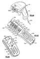
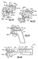
Fig. 8a is an exploded perspective view of an imaging module according to the invention; -
Figs 8b and 8c are front and side views, respectively, of the imaging module shown inFig. 8a ; -
Fig. 8d shows an illumination and aiming pattern which may be projected by an optical reader according to the invention; -
Fig. 8e is a top view of an alternative imaging module incorporating a laser based aiming pattern generating system; -
Fig. 8f is a front view of a polarizer plate which may be included as part of an imaging module herein, e.g., the imaging middle shown inFig. 8a ; -
Figs 9a and 9b are physical form views of various hand held optical readers according to the invention; -
Fig. 9c is a perspective view of a hand held mobile telephone (a "cell phone") which may incorporate a hybrid monochrome and color image sensor array according to the invention and which may be configured according to the invention; -
Fig. 10 is a schematic view of a system incorporating a plurality of optical readers according to the invention; -
Fig. 11 is an application schematic view illustrating an optical reader according to the invention being operated to capture image data representing a parcel that carries a plurality of bar code symbols; -
Fig. 12a is an application schematic view illustrating a first optical reader according to the invention and a second remotely located optical reader according to the invention being operated to take first and second digital pictures of a parcel at first and second locations that are a distance apart for purposes of determining whether the parcel was damaged during delivery from the first location to the second location; -
Fig. 12b is another application schematic view illustrating an optical reader being used to take a color picture of a delivery vehicle; -
Fig. 13a is an application schematic diagram according to the invention illustrating an optical reader according to the invention being used to read bar codes of a vehicle and to take color pictures of a vehicle; -
Fig. 13b is a view of a VIN sticker which may be disposed on the vehicle ofFig. 13 a; -
Fig. 13c is a view of a VIN plate which may be disposed on the vehicle ofFig. 13a ; -
Fig. 13d is a view of a vehicle registration sticker which may be disposed on the vehicle ofFig. 13a ; -
Fig. 13e is a view of an optical reader programmed to display a GUI form assisting an application wherein an optical reader, according to the invention, is utilized to decode bar code symbols and to take color pictures of a vehicle; -
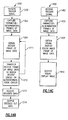
Figs 14a -14c are various flow diagrams illustrating the invention; -
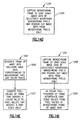
Figs. 14d-14f are additional flow diagrams illustrating examples of operation of an optical reader according to the invention in an indicia decode mode of operation; -
Figs. 14g and 14h are additional flow diagrams illustrating examples of operation of an optical reader according to the invention in a picture taking mode of operation; -
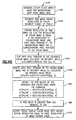
Fig. 14i is a flow diagram illustrating operation of a fusion circuit of an optical reader according to the invention which processes monochrome and color image data to produce a high resolution visual display color frame of image data; -
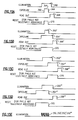
Figs 15a-15e are various image capture initiation control signal timing diagrams illustrating the invention; -
Figs. 16a-16c illustrate various pixelized frames of image data which may be captured by an optical reader according to the invention; -
Fig. 17a is an electrical block diagram of an optical reader according to the invention having a plurality of imaging modules; -
Figs. 17b and 17c illustrate alternative hardware blocks that can be utilized with the electrical circuit ofFig. 17a ; -
Figs. 17d and 17e illustrate imaging modules which may be utilized with the reader ofFig. 17a ; -
Figs. 17f and 17g illustrate exemplary optical readers incorporating a pair of imaging modules; -
Fig. 18a is a schematic view of a cyan-magenta-yellow (CMY) image sensor array in accordance with the invention which may be incorporated into an optical reader according to the invention and which may be controlled to generate both a decode frame of image data and a visual display color frame of image data; -
Fig. 19a is a schematic view of a hybrid monochrome and polarizer image sensor array in accordance with the invention which may be incorporated in an optical reader according to the invention; -
Fig. 19b is a top perspective view of a hybrid monochrome and polarizer image sensor array according to the invention with an exploded view section illustrating a pattern of light polarizing pixels that may be distributed throughout the image sensor array; -
Fig. 19c is a flow diagram illustrating an exemplary operational mode of an optical reader according to the invention which incorporates a hybrid monochrome and polarizer image sensor array according to the invention; -
Figs. 20a and20b are top perspective views of a monochrome polarizer and color sensitive image sensor array according to the invention with an exploded view section illustrating a pattern of light polarizing pixels and color sensitive pixels that may be distributed throughout the array; -
Fig. 21 is a schematic view of an image sensor integrated circuit chip incorporating an image sensor array having color sensitive pixels disposed therein with two different periods of distribution; -
Fig. 22a is a schematic block diagram of an autodiscrimination circuit which may be utilized with the invention; -
Fig. 22b is a process for practicing principles of the invention including automatically discriminating between different dataform types; -
Fig. 22c shows one embodiment of a plurality of curvelent detector maps which may be utilized with the invention; -
Fig. 22d shows another embodiment of a plurality of curvelent detector maps which may be utilized with the invention; -
Fig. 22e is a diagrammatic representation of a histogram analysis which may be performed in one embodiment of the invention; -
Figs. 22f-22i are diagrammatic representations of an image data segmentation process according to embodiments of the invention. - An electrical block diagram of an
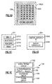
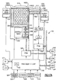
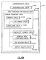
optical reader 100 according to the invention is shown inFig. 1a .Reader 100 includes a solid stateimage sensor array 182A, incorporated on an image sensor integratedcircuit chip 1082A shown inFig. 1a as a CMOS image sensor integrated circuit (IC) chip. In an important aspect, as will be described herein,image sensor array 182A includes a plurality of pixels and wavelength sensitive color filter elements associated with a color sensitive subset of the pixels, wherein the remaining pixels external to the color sensitive subset of pixels are devoid of associated wavelength selective filter elements. Becauseimage sensor array 182A includes both monochrome pixels and color sensitive pixels,image sensor array 182A may be termed a hybrid monochrome and color image sensor array.Reader 100 further includes aprocessor IC chip 548 and acontrol circuit 552.Control circuit 552 in the embodiment ofFig. 1a is shown as being provided by a central processing unit (CPU) ofprocessor IC chip 548. In other embodiments,control circuit 552 may be provided by e.g., a programmable logic function execution device such as a field programmable gate array (FPGA) or an application specific integrated circuit (ASIC).Imaging lens 212 focuses images onto an active surface ofimage sensor array 182A and together withimage sensor array 182A forms animaging assembly 200.Control circuit 552 executes picture taking and indicia decoding algorithms in accordance with instructions stored inprogram memory EPROM 562 which together withRAM 560 andFlash memory 564 forms areader memory 566.Reader memory 566 is in communication withprocessor IC chip 548 viasystem bus 570. Mainprocessor IC chip 548 may be a multifunctional IC chip such as an XSCALE PXA25x processor IC chip including central processing unit (CPU) 552.Reader 100 further includes a field programmable gate array (FPGA) 580. Operating under the control ofcontrol circuit 552,FPGA 580 receives digital image data from imagesensor IC chip 1082A and transfers that image data intoRAM 560 so that the image data can be further processed (e.g., by the decoding of a bar code symbol).Processor IC chip 548 can include an integrated frame grabber. For example,processor IC chip 548 can be an XSCALE PXA27X processor IC chip with "Quick Capture Camera Interface" available from INTEL. Whereprocessor IC chip 548 includes an integrated frame grabber, the integrated frame grabber may provide the frame acquisition functionality ofFPGA 580.Reader 100 further includes anillumination assembly 104 and amanual trigger 216. Imagesensor IC chip 1082A in the embodiment ofFig. 1a includes an on-chip control/timing circuit 1092, an on-chip gain circuit 1084, an on-chip analog-to-digital converter 1086 and an on-chip line driver 1090. An image sensor array which is incorporated intooptical reader 100 may take on a variety of forms. InFig 1a reader 100 includes firstimage sensor array 182A. However, as indicated byhardware block 208, theimage sensor array 182A may be replaced. For example, in the embodiment ofFig. 1b ,reader 100 incorporatesimage sensor array 182B. In other embodiments,optical reader 100 incorporates more than one image sensor array. Various embodiments of image sensor arrays which may be incorporated intoreader 100 are described herein. - In a further aspect,
reader 100 includes a radio frequency (RF)communication interface 571. Radiofrequency communication interface 571 may include one or more radio transceivers. Referring to the schematic diagram ofFig. 1c , radiofrequency communication interface 571 may include one or more of an 802.11radio transceiver 5712, aBluetooth radio transceiver 5714, a GSM/GPS radio transceiver 5716 or a WIMAX (802.16)radio transceiver 5718. Radiofrequency communication interface 571 facilitates wireless communication of data betweendevice 100 and a spaced apartdevice 150. I/O communication interface 572 includes one or more serial or parallel hard-wired communication interfaces facilitating communication with a spaced apartdevice 150 as will be described further in connection withFig. 10 . I/O communication interface 572 may include one or more of an Ethernet communication interface, a universal serial bus (USB) interface, or an RS-232 communication interface.Optical reader 100 may further include akeyboard 508 for entering data, apointer mover 512 for moving a pointer of a graphical user interface (GUI) and atrigger 216 for initiating bar code reading and/or picture taking.Optical reader 100 may also include adisplay 504, such as a monochrome or color LED display and atouch screen 504T overlaid overdisplay 504. As shown in the schematic block diagram ofFig. 1d ,display 504 may include adisplay screen 5042 coupled todisplay controller 5044 for displaying color image data.Display controller 5044 receives a visual display color frame of image data fromcontrol circuit 552, and reformats that data for display depending on the particular requirements ofdisplay screen 5042, including the pixel resolution ofdisplay screen 5042. All of the components ofFig. 1a can be encapsulated and supported by a hand heldhousing 101, e.g., as shown inFigs. 9a-9c . Additional features and functions of the components ofreader 100 shown inFig. 1a are described herein. - Referring to
Fig. 1e ,optical reader 100 may be regarded as having various processing circuits (modules). Indicia decodecircuit 1702 receives image data and decodes decodable indicia therein such as bar code indicia and OCR character data.Optical reader 100 can be configured so that indicia decodemodule 1702 decodes such bar code symbols UPC/EAN,Code 11, Code 39, Code 128, Codabar,Interleaved 2 of 5, MSI, PDF417, MicroPDF417, Code 16K, Code 49, MaxiCode, Aztec, Aztec Mesa, Data Matrix, Qcode, QR Code, UCC Composite, Snowflake, Vericode, Dataglyphs, RSS, BC 412, Code 93, Codablock, Postnet (US), BPO4 State, Canadian 4 State, Japanese Post, KIX (Dutch Post), Planet Code and the like, and such OCR character forms as OCR A, OCR B, and the like.Autodiscrimination circuit 1704 processes received image data and distinguishes between handwritten character data and decodable indicia.Autodiscrimination circuit 1704 may include indicia decodecircuit 1702.Autodiscrimination circuit 1704 and indicia decodecircuit 1702 may be physically embodied by a combination ofcontrol circuit 552 andmemory 566. Specifically,control circuit 552 operating under the control of a program stored inmemory 562 may process image data stored inmemory 560 to decode decodable indicia therein or to discriminate between handwritten character data and decodable indicia. Further aspects of indicia decodecircuit 1702 andautodiscrimination circuit 1704 are described in copendingU. S. Patent Application No. 10/958,779 U. S. Patent Application No. 11/077,975, filed March 11, 2005 entitled, Bar Code Reading Device With Global Electronic Shutter Control, both of which are incorporated herein by reference. As will be described further herein,optical reader 100 may further include ademosaicing circuit 1706, and afusion circuit 1708.Demosaicing circuit 1706 receives as an input a color filter array image data frame (e.g., a Bayer pattern image) and produces as an output a visual display color frame of image data.Fusion circuit 1708 receives as inputs both monochrome and color image data and produces as an output a visual display color frame of image data having a spatial resolution at or on the order of the pixel resolution of the optical reader's hybrid monochrome and color image sensor array. Likecircuit circuits control circuit 552 andmemory 566.Control circuit 552 as well ascircuits Figs. 9a-9c ) or else one or more ofcircuits device 150 as described in connection withFig. 10 . - A visual display color frame of image data as referred to herein, in one embodiment is an image frame including a set of color indicating data at each of a plurality of pixel positions, wherein each set of color indicating data represents a color at a discrete position of a target 1850 (shown in
Fig. 8d ). Each set of color indicating data includes three color values, e.g., a color scale value representing red, a color scale value representing blue, and a color scale value representing green. Alternatively, the set of color indicating data for each pixel position may include a cyan value, a magenta value and a value representing yellow. - In one specific example, the set of color indicating data for each pixel position of a visual display color frame of image data output by
demosaicing circuit 1706 orfusion circuit 1708 are RGB data sets including 24 bits of information, wherein the first 8 bits represent a red color scale value (red value) for the pixel position, the second 8 bits represent a green color scale value (green value) for the pixel position and the third 8 bits represent a blue color scale value (blue value) for the pixel position. - A major feature of the invention is the construction of the optical reader's image sensor array various embodiments of which are shown and described throughout several views including the views of
Figs. 2a-7d . - A first embodiment of a hybrid monochrome and color sensitive (monocolor) solid state image sensor array is shown and described in
Fig. 1 a andFigs. 2a-4b . - Referring to
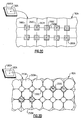
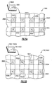
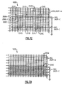
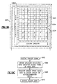
Fig. 1a andFigs. 2a-4b , solid stateimage sensor array 182A includes a monochrome first subset ofpixels 250M and a color sensitive second subset ofpixels 250C. The first subset ofmonochrome pixels 250M is formed in a checkerboard pattern and voids 253 as shown inFig. 2a are formed at the corners of pixels of the first subset, such that combinations of voids, e.g., voids 253-1, 253-2, 253-3, 253-4 of adjacent pixels define open areas, e.g.,open area 255, each open area bounded by four pixels of the first subset. With further reference toimage sensor array 182A,pixels 250C forming a second subset ofpixels 250C are disposed in theopen areas 255, and wavelength selective filter elements, e.g.,filter element Fig. 2b are formed on pixels of the second subset but not on pixels of the first subset.Monochrome pixels 250M as described herein are devoid of color filter elements (color filters). Pixels of the first monochrome pixel subset are in the shape of twelve sided polygons. The pixels are cross-shaped as seen from the top view that is indicated byFigs. 2a-2d (the monochrome pixels are square shaped as modified by the presence of voids 253). Pixels of the color sensitive second subset are square as seen from a top view. - In the version of
image sensor array 182A shown inFig. 2b , colorsensitive pixels 250C ofimage sensor array 182A include either a cyan (Cy)filter element 260C or magenta (Mg)filter element 260M. In the version ofFig. 2c , colorsensitive pixels 250C ofimage sensor array 182A include either ared filter element 260R, agreen filter element 260G or a bluecolor filter element 260B (RGB filters). The colorsensitive pixels 250C can be distributed throughoutimage sensor array 182 according to a Bayer pattern wherein there are N blue pixels, N red pixels and 2N green pixels. Color filter elements of any image sensor array pixel as described herein can be deposited on the major body of colorsensitive pixels 250C by way of a depository process. As will be explained herein, visual display color image data can be obtained utilizing either the version ofimage sensor array 182A shown inFig. 2b or the version ofimage sensor array 182A shown inFig. 2c , or another version ofimage sensor array 182A such as a version including cyan, magenta and yellow (CMY) color sensitive pixels. Because cyan and magenta filters require only one dye and not two dyes (as in red, green, and blue filters) a version ofimage sensor array 182A including cyan and magenta filter elements in place of red, green and blue filter elements allows more light to pass through to a photodetector of the pixels and exhibits a higher signal to noise ratio than a version including red, green and blue filters. Nevertheless, an image sensor array having a combination of red, green and blue (RGB) filter elements may be preferred for certain applications. Referring toFig. 2d ,image sensor array 182A may includemicrolenses 320 for directing of light rays incident onimage sensor array 182A. Further aspects ofmicrolenses 320, including monochrome pixels,microlenses 320M, and colorsensitive pixel microlenses 320C are described herein. - Exploded physical form views of an image
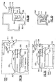
sensor pixel array 182A, wherearray 182A is configured to operate in a global electronic shutter operating mode are shown and described inFigs. 3a-3d . Amonochrome pixel 250M ofimage sensor array 182A is shown inFigs. 3a and 3b .Monochrome pixel 250M includes aphotodetector 302 which may be of photodiode or photogate construction, atransfer gate 304, a floatingdiffusion 306, areset transistor 307 includingreset gate 308, a rowselect transistor 309 including rowselect gate 310 and a sourcefollower amplifier transistor 311 includingamplifier gate 312. An important feature ofpixel 250M is opaqueoptical shield 316. Opaqueoptical shield 316, typically comprising metal, shields light rays from components ofpixel 250M other thanphotodetector 302. Accordingly, pixels from each of several rows ofimage sensor array 182A can be simultaneously exposed to light in a global electronic shutter operating mode without the light rays modulating charges stored in floatingdiffusion 306 or another storage region. Further aspects of image sensor arrays capable of operating in a global electronic shutter operating mode are described inU. S. Patent Application No. 11/077,975 incorporated herein by reference. Referring to additional aspects ofpixel 250M,pixel 250M includesmicrolens 320 which may be disposed on light transmissiveprotective layer 322.Microlens 320 collects light from a larger surface area thanphotodetector 302 and directs light towardphotodetector 302. - A color
sensitive pixel 250C ofimage sensor array 182A is described with reference toFigs. 3c and 3d . Colorsensitive pixel 250C is similar in construction tomonochrome pixel 250M. Colorsensitive pixel 250C includes aphotodetector 302 which may be of photodiode or photogate construction, atransfer gate 304 for transferring charge fromphotodetector 250C, a floatingdiffusion 306, areset transistor 307 includingreset gate 308, a rowselect transistor 309 including rowselect gate 310 and a sourcefollower transistor amplifier 311 includingamplifier gate 312. Colorsensitive pixel 250C also includesopaque shield 320 which shields light from light sensitive components ofpixel 250C other thanphotodetector 302.Pixel 250C may also includemicrolens 320 for increasing the amount of light incident onphotodetector 302. In addition to the above elements colorsensitive pixel 250C includes a wavelength selectivecolor filter element 260 formed thereon. Wavelength selectivecolor filter element 260 may be disposedintermediate microlens 320 andprotective layer 322. In the versions ofFigs. 2a-2d , it is seen that each colorsensitive pixel 250C has four adjacentmonochrome pixels 250M. -
Microlenses 320 as shown inFigs. 3a and 3c are also shown in the view ofFig. 2d .Monochrome pixel microlens sensitive microlens sensitive pixels 250C are disposed in open areas defined by voids of checkerboard pattern of a first monochrome subset ofpixels 250M,microlenses 320C of colorsensitive pixels - Color
sensitive pixel 250C ofimage sensor array 182A as best seen by a comparison betweenFigs. 3b and 3d and consumes a smaller surface area thanpixel 250M. In one version,pixel 250M includes an area, as seen from a top view, of about 12µm by 12µm whilepixel 250C includes an area, as seen from a top view, of about 6µm by 6µm. In another version,pixel 250M includes a top surface area of about 6µm by 6µm, whilepixel 250C includes a top surface area of about 3µm or 3µm. Size reductions ofpixel 250M orpixel pixel 250M and/orpixel 250C. - A transistor count of a
pixel 250C ofimage sensor array 182A may readily be reduced by eliminating optically shielded floatingdiffusion 306 in which charges are stored on a temporary basis to facilitate global electronic shutter operation. Accordingly, in one embodiment,monochrome pixels 250M ofimage sensor array 182A have more transistors than colorsensitive pixels 250C but are capable of being exposed on a global electronic shutter basis, whereas colorsensitive pixels 250C have fewer transistors thanmonochrome pixels 250M but are not capable of being exposed on a global electronic shutter basis. In yet another embodiment with reference toimage sensor array 182A having smaller dimensioned color sensitive pixels than monochrome pixels, the relatively largermonochrome pixels 250M have a transistor count sufficient to facilitate global shutter operation, but the relatively smaller colorsensitive pixels 250C are passive pixels requiring off-pixel amplification, and comprise a single transistor each. Further aspects of global electronic shutter and rolling shutter operations relative to image sensor arrays which may be incorporated intoreader 100 are described herein. - Referring to
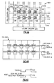
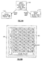
Fig. 4a , a high level electrical block diagram ofimage sensor array 182A is shown. According to one version,image sensor array 182A is an active pixel image sensor array of complementary metal oxide semiconductor (CMOS) construction such that eachpixel pixel amplifier 311 for amplifying signals corresponding to light incident onphotosensitive region 252. Eachpixel storage element 306.Image sensor array 182A further includes two-dimensional grid ofinterconnects 262 which are in electrical communication withrespective column circuitry 270 androw circuitry 296.Row circuitry 296 andcolumn circuitry 270 enable such processing and operational tasks as selectively addressing pixels, decoding pixels, amplification of signals, analog-to-digital conversion, applying timing, read out and reset signals and the like. - Among the control lines forming
interconnect grid 262 ofimage sensor array 182A are pixel reset control lines. When pixels are reset by application of an appropriate control signal on a reset control line, residual charges which have accumulated on the pixels are connected temporarily to VDD so that built up charges on pixels of the image sensor array drain out of the pixels. In accordance with the invention,image sensor array 182A includes separate reset control lines formonochrome pixels 250M andcolor pixels 250C. Referring toFig. 4b ,image sensor array 182A may be constructed so thatimage sensor array 182A has a first set ofreset control lines 262R-M for resettingmonochrome pixels 250M and a second set ofreset control lines 262R-C for resettingcolor pixels 250C. - In certain operating modes
optical reader 100 selectively reads out a windowed frame of image data comprising image data frommonochrome pixels 250M. In other operating modes,optical reader 100 selectively reads out a windowed frame of image data comprising image data fromcolor pixels 250C. In accordance with the invention, a reset control timing pulse can be applied toimage sensor array 182A during the time that a windowed frame of image data is being captured to reset pixels ofimage sensor array 182A that are not being selectively addressed for image data read out. As shown by the timing diagram ofFig. 4c , an exposurecontrol timing pulse 354 can be coordinated with a resetcontrol timing pulse 370. - With further reference to
Fig. 4c , exposurecontrol timing pulse 354 may control exposure ofmonochrome pixels 250M ofimage sensor array 182A (or alternatively,color pixels 250C) ofimage sensor array 182A, while resetcontrol timing pulse 370 drives pixels not being selectively addressed into a reset state. When pixels are reset, charges built up on pixels tend to be drained out of the pixels. Further, it is believed that photons entering pixels driven into reset may be refracted so that fewer photons become incident on neighboring pixels being exposed for image data read out. Accordingly, coordinating the timing of anexposure control pulse 354 for exposing selectively addressed pixels and a resetcontrol timing pulse 370 for resetting pixels not being selectively addressed reduces cross talk between pixels. - Referring again to the view of
Fig. 4b ,image sensor array 182A may be constructed so that the presence of multiple reset control lines 162R-C, 162R-M do not substantially decrease the fill factor of pixels ofimage sensor array 182A.Fig. 4b shows a schematic top view of multiple reset control lines 162R-M, 162R-C incorporated inimage sensor array image sensor array 182A in a layered manner so that for a substantial portion ofimage sensor array 182A, control lines 164R-M have x, y positions that coincide with x, y positions of control line 164R-C (axes are defined inFig. 8a ). Control lines 164R-C in the embodiments ofFig. 4b are installed at a different height (a different Z axis position) withinimage sensor array 182A such that control lines 162R-M and 162R-C, for substantial length of the control lines, have common x, y positions. Installing the multiple control lines to be on top of one another so that the control lines have a common x, y axis position withinimage sensor array 182A reduces the amount of fill factor degradation which would otherwise result from installation of an additional set of reset control lines withinimage sensor array 182A. - An alternative construction for an image sensor array according to the invention is described with reference to
Figs. 5a-7b . In the embodiment ofFigs. 5a-7b image sensor array 182B includes a plurality of square shaped pixels (as seen from a top view) in a checkerboard pattern, each of the pixels having substantially the same dimensions. Eachpixel image sensor array 182B may be constructed to have approximately the same top surface dimensions as seen from the top views ofFigs. 5a-5i and approximately the same side view cross-sectional dimensions as seen from the cross-sectional views ofFigs. 6a-6d .Image sensor array 182B is similar to the construction of a standard off-the-shelf monochrome image sensor array except that select ones of the pixels of the image sensor array have an associated wavelength selective color filter element. Solid stateimage sensor array 182B includes a plurality of pixels formed in a plurality of rows. In the version ofFigs. 5a-5e , a monochrome first subset ofpixels 250M comprise the majority of pixels of the array. Wavelength selectivecolor filter elements 260 are included in the second subset of colorsensitive pixels 250C. The color sensitive second subset ofpixels 250C comprises pixels at spaced apart pixel positions uniformly distributed or substantially uniformly distributed throughout the plurality of pixels forming theimage sensor array 182B. In the embodiment ofFigs. 5a and 5b , every other pixel in every other row of pixels (e.g.,pixel row image sensor array 182B can be provided by including an appropriately designed color filter array on an image sensor array of an MT9M111 Digital Clarity SOC 1.3 megapixel CMOS image sensor IC chip of the type available from Micron, Inc., an MT9V022 image sensor IC chip also available from Micron, Inc. or a W6600 1.3 megapixel CMOS image sensor IC chip of the type available from STMicroelectronics. Other image sensor IC chips which can be utilized to provideimage sensor array 182B include MT9M413 image sensor IC chip available from Micron, Inc., a KAC-0311 image sensor IC chip manufactured by Kodak, Inc. and a KAI-0340 image sensor IC chip also manufactured by Kodak, Inc. Operational aspects of the referenced KAI-0340 image sensor IC chip are described further herein. Various manufacturer product description materials respecting certain of the above image sensor IC chips are appended toU. S. Provisional Patent Application No. 60/692,890 filed June 22, 2005 U. S. Provisional Patent Application No. 60/694,371 filed June 27, 2005 image sensor arrays - The above referenced MT9V022 and MT9M413 image sensor IC chips manufactured by Micron, Inc., and KAC-0311 image sensor IC chip by Kodak, Inc. are CMOS image sensor IC chips that may be operated in a global electronic shutter mode such that all rows of pixels subject to image data read out have common exposure periods; that is, all rows of pixels subject to image data read out for reading out a frame of image data (i.e., full frame or "windowed frame") have a common exposure start time and a common exposure stop time. For global electronic shutter operation, an exposure control timing pulse, as will be described herein is applied to the image sensor array. Exposure of each row of pixels subject to image data read out begins at the leading edge of the exposure control timing pulse and ends at the falling edge of the exposure control timing pulse. In its technical literature, Micron, Inc. uses the trademark TRUESNAP with reference to a global electronic shutter operating mode.
- Referring to
Fig. 5b , wavelength selective color filter elements (filters) formed on colorsensitive pixels cyan filter elements 260C and magentacolor filter elements 260M. As shown inFig. 5a , wavelength sensitive filters of colorsensitive pixels 250C may also be a combination ofred filter elements 260R,green filter elements 260G andblue filter elements 260B. Because cyan and magenta filters require only one dye and not two dyes (as in red green and blue filters), the version ofFig. 5b allows more light to pass through to a photodetector (e.g.,photodetector 302 as shown inFig. 6c ) and exhibits a higher signal to noise ratio than the embodiment ofFig. 5b . Nevertheless, the version ofFig. 5a may be preferred for certain applications. - In the embodiment of
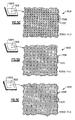
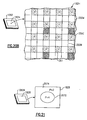
Figs. 5a-7d , hybrid monochrome andcolor image sensor 182B can be made by including an appropriately designed color filter array on a commonly available, off-the-shelf image sensor array in a standardly known checkerboard pattern, each pixel of the array having substantially the same dimensions. A larger portion ofimage sensor array 182B is shown inFig. 5c , where pixels designated by the letter "c" are colorsensitive pixels 250C and pixels not designated by the letter "c" aremonochrome pixels 250M. In the example ofFig. 5c , color sensitive pixels are formed onarray 182B with a period of P=2, meaning the every other pixel of every other row of pixels is a colorsensitive pixel 250C. In the version ofFig. 5d , color sensitive pixels are formed onarray 182B with a period of P=3, meaning that every third pixel of every third row is a colorsensitive pixel 250C. In the version ofFig. 5e , color sensitive pixels, c, are formed with a period of P=4, meaning that every fourth pixel from every fourth row of pixels is a colorsensitive pixel 250C. In the versions ofFigs. 5a-5e , each colorsensitive pixel 250C has eight adjacentmonochrome pixels 250M (two side adjacent, one top adjacent, one bottom adjacent and four corner adjacent). - Additional views of
image sensor array 182B including a subset ofmonochrome pixels 250M and a subset of colorsensitive pixels 250C, wherein each pixel of the image sensor array has substantially equal dimensions are shown and described in connection withFigs. 5f-5j . - Referring to the version of
Fig. 5f ,image sensor array 182B includes the first subset ofmonochrome pixels 250M and a second subset of colorsensitive pixels 250C. The colorsensitive pixels 250C ofimage sensor array 182B in the version ofFig. 5f are formed in clusters such ascluster 257R,cluster 257G andcluster 257B. - Each cluster 257 in the version of
Fig. 5f includes a plurality of pixels in successive horizontally adjacent pixel positions, such that each pixel of the cluster is horizontally adjacent to at least one other color sensitive pixel. Color sensitive clusters of pixels are distributed uniformly or substantially uniformly throughoutimage sensor array 182B. Clusters may be formed in accordance with the standardized color filter pattern such as an RGB Bayer pattern or a cyan-magenta-yellow (CMY) pattern. Each cluster may have a plurality of pixels with each pixel of every individual cluster having a filter element of the same wavelength rating. In the specific version shown inFig. 5f , clusters are distributed throughoutimage sensor array 182B in a pattern that is accordance with the pattern of Bayer color filter array. -
Cluster 257G includes three horizontally adjacent green pixels.Cluster 257R includes three horizontally adjacent red pixels.Cluster 257B includes three horizontally adjacent blue pixels. As will be described further in connection withFig. 7c , the version ofimage sensor array 182B including a distribution of color sensitive pixels in horizontally arranged clusters as shown inFig. 5f is particularly useful where it is desired to include inimage sensor array 182B separate and independently controllablereset control lines 262R-M and 262R-C for separately and independently resetting monochrome pixels ofimage sensor array 182B and color sensitive pixels of imagesensory array 182B without increasing the thickness ofimage sensor array 182B. - Referring now to the versions of
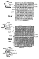
image sensor array 182B shown inFig. 5g-5j ,image sensor array 182B having a subset of monochrome pixels in a subset of color sensitive pixels may be configured to include "zones" of monochrome pixels and "zones" of color sensitive pixels. A "zone" of pixels herein is a collection of positionally related pixels at a specified area of an image sensor array each having a color filter element or alternatively, each being without a color element. Examples of zones described herein comprise all pixels of one row of pixels or all pixels of each of several consecutive rows of pixels. In the version ofFig. 5g ,image sensor array 182B includes two color sensitive zones ofpixels 2500C and a single monochrome zone ofpixels 2500M. Each zone of pixels comprises a plurality of horizontally, vertically or diagonally adjacent pixels. The plurality of pixels of a monochrome zone of pixels, e.g.,zone 2500M are all devoid of a color sensitive filter element. The plurality of adjacent pixels in a color sensitive zone of pixels, e.g.,zone 2500C, all include a color sensitive filter element. - Referring to the version of
Fig. 5g , monochrome zone ofpixels 2500M is interposed between a pair of color sensitive zones ofpixels 2500C. Monochrome zone ofpixels 2500M in the version ofFig. 5g comprises a single row of pixels ofimage sensor array 182B at or approximately the center ofimage sensor array 182B. The first color sensitive zone of pixels of animage sensor array 182B includes all pixels from the row of pixels ofzone 2500M up to the top row ofimage sensor array 182B. The second color sensitive zone ofpixels 2500C in the version ofFig. 5g includes all pixels from all rows from the center row monochrome zone ofpixels 2500M down to the bottom row of pixels ofimage sensor array 182B. The color filter elements of colorsensitive pixels 250C ofimage sensor array 182B may be formed in a standard color filter pattern, e.g., an RGM Bayer color filter pattern or a CMY pattern. - Referring to
Fig. 5h , another version ofimage sensor array 182B is shown and described. The version ofFig. 5h is similar to the version ofFig. 5g except that the monochrome zone ofpixels 2500M is expanded to include ten consecutive rows of pixels at the center or approximately the center ofimage sensor array 182B. - In the version of
image sensor array 182B as shown inFig. 5i , a single color sensitive zone ofpixels 2500C is interposed between two relatively small width monochrome zones ofpixels 2500M formed at the top and bottom ofimage sensor array 182B respectively. In the version ofimage sensor array 182B shown inFig. 5a , the first monochrome zone ofpixels 2500M comprises the first ten rows of pixels ofimage sensor array 182B and a second monochrome zone ofpixels 2500M includes pixels of the bottom ten rows ofimage sensor array 182B. Color sensitive zone ofpixels 2500C in the version ofFig. 5i includes all pixels of the array excluding the first ten and the last ten rows of pixels ofimage sensor array 182B. In the versions ofFigs. 5h and Fig. 5i , the pixels of the colorsensitive zones 2500C shown may include color filter elements in accordance with the pattern of a standardized color filter array, e.g., an RGB Bayer pattern or a CMY pattern. - The version of
image sensor array 182B shown inFig. 5j is similar in construction to the version ofFig. 5g except that the version ofFig. 5j includes additional monochrome zones ofpixels 2500M. In the version ofFig. 5j image sensor array 182B includes a pair of diagonal zones ofmonochrome pixels 2500M-D extending through a center (actual or approximate) ofimage sensor array 182B and a vertically extending zone ofmonochrome pixels 2500M-V extending through a center ofimage sensor array 182B. The linear zones ofmonochrome pixels 2500M shown in the version ofFig. 5j may include a minor dimension equal to one pixel width or more than one pixel width. For example, the vertically extending monochrome zone ofpixels 2500M ofFig. 5j may include pixel positions of one column of pixels or of a plurality of columns of pixels. Likewise, the diagonally extending linear monochrome zones ofpixels 2500M ofFig. 5g may include pixel positions of a single diagonal row of pixels or alternatively, of a plurality of diagonal rows of pixels. - It will be seen that the versions of
image sensor array 182B shown inFigs. 5g-5j are particularly well suited for use in picture taking optical readers which in bar code decoding applications are expected to decode linear bar code symbols. The image sensor arrays ofFigs. 5g-5j may be referred to as linear symbol optimized image sensor arrays. As will be described in further detail herein, image data corresponding to monochrome zones ofpixels 2500M in the versions ofFigs. 5g-5j can be selectively addressed and read out independently of image data from rows from colorsensitive zones 2500C of pixels. In bar code decoding applications,control circuit 552 may selectively address pixels ofmonochrome zones 2500M and read out image data from monochrome zones ofpixels 2500M as shown inFigs. 5g-5i and transfer such image data to indicia decodecircuit 1702 for decoding of a linear bar code symbol. For picture taking applications,control circuit 552 may selectively address pixels of a color sensitive zone or zones ofpixels 2500C and selectively read out image data from color sensitive zone orzones 2500C and process such color image data into a visual display color frame of image data. The processing as will be explained further herein may include such steps as executing a demosaicing routine to convert color filter pattern image data into a visual display format and interpolation of color pixel values corresponding to the missing pixel positions at the pixel positions occupied by a monochrome zone orzones 2500M of pixels. - In
Figs. 6a-6d , exploded physical form view of pixels ofimage sensor array monochrome pixel 250M ofimage sensor array 182B is shown inFigs. 6a and 6b .Pixel 250M includes aphotodetector 302 which may be of photodiode or photogate construction, atransfer gate 304, a floatingdiffusion 306, areset transistor 307 includingreset gate 308, a rowselect transistor 309 including rowselect gate 310 and a sourcefollower amplifier transistor 311 includingamplifier gate 312. An important feature ofpixel 250M is opaqueoptical shield 316. Opaqueoptical shield 316, typically comprising metal, shields light rays from components ofpixel 250M other thanphotodetector 302. Accordingly, pixels fom each or several rows orimage sensor array 182A can be simultaneously exposed to light in a global electronic shutter operating mode without the light rays modulating charges stored in floatingdiffusion 306 or another storage region. Further aspects of image sensor arrays capable of operating in a global electronic shutter operating mode are described inU. S. Patent Application No. 11/077,975 incorporated herein by reference. Referring to additional aspects ofpixel 250M,pixel 250M includesmicrolens 320 which may be disposed on light transmissiveprotective layer 322.Microlens 320 collects light from a larger surface area thanphotodetector 302 and directs light towardphotodetector 302. - A color
sensitive pixel 250C ofimage sensor array 182B is described with reference toFigs. 6c and 6d . Colorsensitive pixel 250C is similar in construction tomonochrome pixel 250M. Colorsensitive pixel 250C includes aphotodetector 302 which may be of photodiode or photogate construction, atransfer gate 304 for transferring charge fromphotodetector 250C, a floatingdiffusion 306, areset transistor 307 includingreset gate 308, a rowselect transistor 309 including rowselect gate 310 and a sourcefollower transistor amplifier 311 includingamplifier gate 312. Colorsensitive pixel 250C also includesopaque shield 320 which shields light from light sensitive components ofpixel 250C other thanphotodetector 302.Pixel 250C may also includemicrolens 320 for increasing the amount of light incident onphotodetector 302. In addition to the above elements, colorsensitive pixel 250C includes a wavelength selectivecolor filter element 260 formed thereon. Wavelength selectivecolor filter element 260 may be disposedintermediate microlens 320 andprotective layer 322. - A high level electrical block diagram of
image sensor array 182B is shown inFig. 7a .Image sensor array 182B may be of CMOS construction and may be an active pixel image sensor array such that eachpixel 250 ofimage sensor array 182B includes apixel amplifier 311. Eachpixel 250 of image sensor array may further have aphotosensitive region 252 and an optically shieldedstorage element 306.Image sensor array 182B further includes a two-dimensional grid ofinterconnects 262 which are in electrical communication withrespective column circuitry 270 androw circuitry 296.Row circuitry 296 andcolumn circuitry 270 enable such processing and operational tasks as selectively addressing pixels, decoding pixels, amplification of signals, analog-to-digital conversion, and applying timing, read out and reset signals. - Reset control lines of
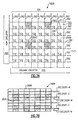
interconnect grid 262 are shown inFig. 7b .Image sensor array 182B may have multiple sets of reset control lines so thatmonochrome pixels 250M ofimage sensor array 182B can be reset independently of colorsensitive pixels 250C ofimage sensor array 182B as described previously in connection with the description ofimage sensor array 182B. According to the invention,control lines 262R-M, 262R-C can be incorporated inimage sensor array 182B in a layered manner so that for a substantial portion ofimage sensor array 182B,control lines 262R-M have x, y positions that coincide with x, y positions ofcontrol line 262R-C (axes are defined inFig. 8a ). Control lines 262R-C in the embodiment ofFigs. 7b are installed at a different height (a different Z axis position) withinimage sensor array 182B relative to controllines 262R-C such that control lines 262R-M and 262R-C, for substantial length of the control lines, have common x, y positions. Installing the multiple control lines to be on top of one another so that the control lines have a common x, y axis position withinimage sensor array 182B reduces the amount of fill factor degradation which would otherwise result from installation of an additional set of reset control lines withinimage sensor array 182B. - Referring to
Figs. 7c and 7d ,image sensor array 182B may be configured to include separate and independent reset control lines for separately and independently resettingmonochrome pixels 250M and colorsensitive pixels 250C without increasing the overall thickness ofimage sensor array 182B. While disposing reset control lines on top of one another as described in connection withFigs. 4b and7b provides significant advantages; the image sensor array is made thicker with such arrangement which adds to manufacturing costs. Referring toFig. 7c , a version ofimage sensor array 182B is illustrated having a first set ofreset control lines monochrome pixels 250M and a second set ofreset control lines sensitive pixels 250C ofimage sensor array 182B. The reset control line configuration ofFig. 7c may be utilized with the color sensitive pixel distribution shown inFig. 5f to provide animage sensor array 182B having separate and independently controllable reset control lines for separately resettingmonochrome pixels 250M and colorsensitive pixels 250C and which exhibits a thickness equal to a thickness of a commonly available off-the-shelf image sensor array. In the version ofimage sensor array 182B shown inFig. 7c , the reset control lines of monochrome pixel rows are electrically connected together and the reset control lines of rows of pixels including color sensitive pixels are electrically connected together. The commonly connected reset control lines of the monochrome pixel rows are designated with thereference numeral reference numeral Fig. 5f andFig. 7c , every fourth row of pixels ofimage sensor array 182B includes clusters of colorsensitive pixels Fig. 7c , withreset control lines sensitive pixels 250C electrically connected together, all rows ofimage sensor array 182B including colorsensitive pixels 250C may be driven into reset by application of a reset control signal on commonreset control line monochrome pixels 250M (the monochrome row of pixels) can be driven into reset by applying a reset control signal on common monochrome pixel resetcontrol line image sensor array 182B shown inFig. 7c ,monochrome pixels 250M ofimage sensor array 182B may be driven into reset whenpixels 250C are exposed for image data read out of color image data. - It is noted that with the configuration of
Fig. 7c , adjacentmonochrome pixels 250M-A adjacent to an end pixel, e.g.,pixel 250C-E of a color sensitive pixel cluster, e.g.,cluster 257R are not driven into reset during exposure periods of colorsensitive pixels 250C. However, according to the invention in one example, image data corresponding only to acenter pixel 250C-I of each color sensitive horizontally arranged cluster (and not theend pixels 250C-E) may be selectively addressed during read out of color image data. The presence of each lateral color filter element at theend pixels 250C-E, which are not addressed for image data read out, reduces the effect of cross talk attributable to photons enteringimage sensor array 182B at an angle throughend pixels - Another configuration for providing separately and independently resetting
monochrome pixels 250M and colorsensitive pixels 250C ofimage sensor array 182B is shown and described with reference toFig. 7d . In the version ofFig. 7d ,image sensor array 182B includes a plurality of rows of pixels including allmonochrome pixels 250M followed by a plurality of rows of pixels that include colorsensitive pixels 250C only. The monochrome rows ofpixels 250M form a first subset of pixels and the colorsensitive pixels 250C form a second subset of pixels. The reset control lines for resetting the first subset of pixels can be made separate and independent of the reset control lines for controlling the second subset of pixels by electrically connecting the reset control lines of the first subset of pixels together and then separately electrically connecting together the reset control lines of the second subset of pixels. The common control lines of the first subset ofmonochrome pixels 250M in the version ofFig. 7d are designated withreference numeral sensitive pixels 250C in the version ofFig. 7d are designated with thereference numeral Fig. 7d facilitating separate and independent control ofmonochrome pixels 250M and colorsensitive pixels 250C can be utilized with the line art symbol optimized versions ofimage sensor array 182B shown and described inFigs. 5g-5i having "zones" of monochrome or alternatively colorsensitive pixels 250C that extend entire rows ofimage sensor array 182B. - Referring to
Fig. 7d , colorsensitive pixels 250C may be driven to reset during exposure periods formonochrome pixels 250M by application of a common reset control signal onreset control line sensitive pixels 250C for read out of color image data. Similarly colorsensitive pixels 250C may be driven into reset by application of a reset control signal on commonreset control line monochrome pixels 250M for read out of image data frommonochrome pixels 250M. - Features respecting specific embodiments of an image sensor array according to the invention have been described in connection with the views of
Figs. 2a-4c (image sensor array 182A), and the views ofFigs. 5a-7d (image sensor array 182B). General features of an image sensor array which may be incorporated into optical reader 100 (that is, features which can be incorporated in the image sensor array, whether of the embodiment labeled 182A, the embodiment labeled 182B, or another embodiment such as CMYimage sensor array 182C, RGBimage sensor array 182D, monochrome linearimage sensor array 182E, monochrome areaimage sensor array 182F, monochrome and polarizerimage sensor array 182G, or monochrome color and polarizerimage sensor array 182H) are now described. -
Optical reader 100 can be programmed or otherwise be configured to selectively address a first plurality of pixels in animage sensor array optical reader 100 selectively addresses the first subset of pixels and reads out image data from first subset of pixels independently of the second color sensitive subset of pixels. In another operating modeoptical reader 100 selectively addresses the second subset of pixels and reads out image data from the second subset of pixels independently of the first subset ofpixels 250M. Whereoptical reader 100 selectively addresses and selectively reads out only a subset of pixels of an image sensor array, the resulting frame of image data read out of the image sensor array may be referred to as a "windowed frame" of image data. When a windowed frame of image data is read out, the frame rate of the image sensor array is normally increased relative to a normal frame rate of the image sensor array. -
Image sensor array - When operated in a global electronic shutter operating mode, pixels from several rows of an image sensor array are exposed simultaneously. That is, when operated in a global electronic shutter operating mode, transistor components (for example, transfer
gates 304 and resetgates 308 of the array as shown in the embodiments ofFigs. 3a and6a ) forming an electronic shutter an image sensor array are controlled in a coordinated manner so that a plurality of rows of pixels are exposed simultaneously and have common exposure periods. In a global electronic shutter operating mode, electronic shutter components of the array are controlled so that the common exposure period for each of the plurality of rows of pixels begins at a common exposure start time (via control of reset gates 308) and ends at a common exposure stop time (via control of transfer gates 304). As explained herein, each pixel of the array may store a charge in an optically shielded storage region during the common exposure period. For facilitating a global electronic shutter operating mode, an exposurecontrol timing pulse image sensor array Figs 15a-15e . An exposurecontrol timing pulse image sensor array control timing pulse control timing pulse -
Image sensor array optical reader 100 may be constructed to be operated in a rolling shutter mode of operation only; that is, in one specific embodiment an image sensor array ofoptical reader 100 can only be controlled to expose pixels of the image sensor array on a rolling shutter basis and cannot be controlled so that pixels of image sensor array are exposed on a global electronic shutter basis. In another embodiment, an image sensor array incorporated inoptical reader 100 is constructed to be operated in a global electronic shutter operational mode only and is incapable of operation in a rolling shutter mode. -
Image sensor array optical reader 100 is constructed to be operational in either of a rolling shutter operational mode or a global shutter operational mode, the switching between rolling shutter and global shutter operational modes may be made in response to a receipt of operator instructions to change the shutter mode. The switching between rolling shutter and global shutter operational modes may also be automatic and dynamic in response to the sensing of a predetermined criteria being satisfied. An image sensor array equippedoptical reader 100 having both rolling shutter and global shutter operational modes is described inU. S. Patent Application No. 11/077,975, filed March 11, 2005 entitled, Bar Code Reading Device With Global Electronic Shutter Control, which is incorporated herein by reference. An image sensor array constructed to be operated in either of a rolling shutter or global shutter operational mode is described inU. S. Patent No. 6,552,323 entitled, "Image Sensor With A Shared Output Signal Line" which is incorporated by reference. -
Image sensor array - It has been described with reference specifically to
image sensor array 182A, andimage sensor array 182B that it may be advantageous to incorporate into an image sensor array ofoptical reader 100 separately controllablereset control lines image sensor array optical reader 100 incorporating a cyan-magenta-yellow (CMY)image sensor array 182C as shown inFig. 18c , it may be advantageous to incorporate separate reset control lines for resetting magenta and cyan pixels separately from yellow pixels so that when yellow pixels are exposed for read out of decode frame yellow pixel image data for transmission to decode circuit 1792, the remainder of the pixels of the array, i.e., the cyan and magenta pixels can be set to reset to eliminate electron diffusion cross talk and to reduce photon penetration cross talk. When hand heldoptical reader 100 incorporates a hybrid monochrome and polarizerimage sensor array 182G as shown inFig. 19b or the monochrome color and polarizerimage sensor array 182H as shown inFigs. 20a and20b , it may be beneficial to incorporate intoimage sensor array 182 separately controllable reset control lines for controlling the reset of pixels external to the polarizing pixels so that when the polarizing pixels are exposed for read out of image data from the polarizing pixels, the remaining pixels of the image sensor array are set to reset to reduce cross talk from the pixels external to the polarizing pixels. - While an
image sensor array image sensor array image sensor array 182B is configured according to the version shown inFig. 5h having center rows of monochrome pixels defining amonochrome pixel zone 2500M and where the image sensor array is a CCD KAI-0340 image sensor array, image data from the center rows can be read out by selecting a preconfigured operating mode of the image sensor array chip. Additional "windowed frame" patterns can be selectively read out of a CCD image sensor array by varying the speed of a pixel clock timing control timing pulse that controls the speed with which a pixel is clocked. Invalid or null data can be clocked out of a CCD pixel by speeding up a pixel clock signal. Varying a pixel clock control signal between valid data yielding rates and invalid data yielding rates during the reading out of image data from a CCD image sensor array yields a windowed frame of image data comprising valid image data clocked out at normal speed and invalid image data clocked out at high speed. Image data can also be selectively read out of a CCD image sensor array by selectively gating to output circuitry of the CCD image sensor array image data corresponding to select pixels of the image sensor array. It will be seen that for any application described herein wherein a windowed frame of image data is read by selective addressing of pixels from a CMOS image array, a CCD image sensor array supporting windowing capability may be substituted therefore to provide selective read out functionality. - Additional aspects of the invention are described with reference to the physical form views of
Figs. 8a-8c and the physical form views 9a, 9b and 9c. In the physical views ofFigs. 8a-8c , an imaging module onto which an image sensor chip may be incorporated is described. With reference toFigs. 9a, 9b and 9c , hand held housings for supporting and encapsulating an imaging module including an image sensor chip are described. - An
optical reader 100 of the invention, as shown in the embodiment ofFigs. 8a-8c , may include an imaging module such asimaging module 1802A.Imaging module 1802A as shown inFigs. 8a-8c incorporates certain features of an IT4000 imaging module herein and additional features. IT4000 imaging modules are available from Hand Held Products, Inc. of Skaneateles Falls, New York.Imaging module 1802A includesfirst circuit board 1804 carrying light sources 160a, 160b, whilesecond circuit board 1806 carries light sources 160c, 160d, 160e, 160f, 160g, 160h, 160i, 160j, 160k, 1601, 160m, 160n, 160o, 160p, 160q, 160r, 160s, and 160t (hereinafter 160c through 160t).First circuit board 1804 also carriesimage sensor array 182, which is integrated onto imagesensor IC chip 1082. Imagesensor IC chip 1082 andimage sensor array 182 inFig. 8a are generically labeled with the reference numerals "1082" and "182" respectively inFigs. 8a-8d to indicate that any one of the specifically described imagesensor IC chips image sensor arrays imaging module 1802A. The various image sensor IC chips and image sensor arrays can also be incorporated in another imaging module described herein such asimaging module Imaging module 1802C shown inFig. 8e is a laser aiming IT4300 imaging module of the type available from Hand Held Products, Inc. The laser aiming IT4300 imaging module includes a plurality of illumination LEDs e.g.,LED 160, and an aiming pattern generator comprising alaser diode assembly 1872 in combination with adiffractive element 1873, wherein the diffractive element of the imaging module diffracts laser light from the laser diode assembly to project a two-dimensional aiming pattern onto a substrate, s,.Imaging module 1802A also includessupport assembly 1810 includinglens holder 1812, which holdslens barrel 1814 that carriesimaging lens 212 that focuses images onto an active surface ofimage sensor array 182.Lens 212 may be e.g., a single lens (a lens singlet), a lens doublet or a lens triplet. Light sources 160a, 160b are aiming illumination light sources whereas light sources 160c through 160t are illumination light sources. Referring toFig. 8d , illumination light sources 160c through 160t project a two-dimensional illumination pattern 1830 over a substrate, s, that carries a decodable indicia such as abar code symbol 1835 whereas aiming illumination light sources 160a, 160b project an aimingpattern 1838. In the embodiments shown and described in connection withFigs. 8a-8c , light from aiming illumination light sources 160a, 160b is shaped byslit apertures 1840 in combination withlenses 1842 which image slits 1840 onto substrate, s, to form aimingpattern 1838 which in the embodiment ofFigs. 8a-8c is aline pattern 1838.Illumination pattern 1830 substantially corresponds to a full frame field of view ofimage reader 100 designated bybox 1850. The present field of view ofoptical reader 100 is herein referred to as the "target" ofoptical reader 100. Aimingpattern 1838 is in the form of a line that extends horizontally across a center of field of view ofimage reader 100.Illumination pattern 1830 may be projected when all of illumination light sources 160c through 160t are operated simultaneously.Illumination pattern 1830 may also be projected when a subset of light sources 160c through 160t are simultaneously energized.Illumination pattern 1830 may also be projected when only one of light sources 160c through 160t is energized such as LED 160s or LED 160t. LEDs 160s and 160t ofimaging module 1802 have a wider projection angle than LEDs 160c through 160t. In anoptical reader 100 incorporatingimaging module 1802A illumination assembly 104 includes LEDs 160a, 160b, LEDs 160c through 160t and slitapertures 1840 in combination withlenses 1842. - A reader imaging module may be incorporated into one of a hand held housing as shown in
Figs. 9a, 9b and 9c . In the embodiment ofFig. 9a , hand heldhousing 101 is a gun style housing. In the embodiment ofFig. 9b , hand heldhousing 101 supportingimaging module 1802 is in the form factor of a portable data terminal (PDT). In the embodiment ofFig. 9c , hand heldhousing 101 supporting imaging module is in the form factor of a mobile telephone, often referred to as a "cell phone." Whenoptical reader 100 is a cell phone,optical reader 100 is configured to send voice data over GSM/GPRS transceiver 571 to GSM/GPRS network 198 (Fig. 10 ) and to receive over GSM/GPRS transceiver 571 voice data from GSM/GPRS network 198. Further, whereoptical reader 100 is a cell phone,optical reader 100 may be configured so that an operator inputs telephone numbers viakeyboard 508. Thespecific imaging module 1802A described in connection withFigs. 8a-8c may be incorporated in the optical reader shown inFig. 9a or theoptical reader 100 shown inFig. 9b or theoptical reader 100 shown inFig. 9c . However, in the embodiment shown inFig. 9a ,housing 101 supports and encapsulatesimaging module 1802B an imaging module of construction similar toimaging module 1802A, except that only twolight sources 160 are incorporated into the imaging module.Housing 101 of the reader ofFig. 9b supportsimaging module 1802 which is generically labeledelement 1802 to indicate that any one of the specific imager modules described herein, e.g., 1802, 1802A, 1802B, 1802D, 1802E may be incorporated into an optical reader according to the invention. - Referring to further aspects of
optical reader 100,optical reader 100 may incorporate a graphical user interface (GUI) 3170 enabling selection between various operating modes. WithGUI 3170 an operator movespointer 3172 to a selected icon and clicks on the icon to configureoptical reader 100 in accordance with an operating mode associated with the selected icon.Reader 100 may include pointer mover 512 (otherwise termed a navigation matrix) to facilitate movement of thepointer 3172.Buttons 512B ofpointer mover 512 facilitate selection of an icon of a GUI interface that is supported by incorporating a multitasking operating system (OS) intoreader 100 such as WINDOWS CE.GUI 3172 may be developed using various open standard languages as HTML/Java or XML/Java. - In the embodiment of
Fig. 9b ,GUI 3170 includes a plurality ofvirtual selection buttons shutter icon 3152 configuresreader 100 so that during a next exposure periodimage sensor array 182 is operated in a rolling shutter mode. Selection ofglobal shutter icon 3154 configuresoptical reader 100 so that during a next exposure periodimage sensor array 182 is operated in a global electronic shutter mode. - Selection of
decode icon 3162 drivesoptical reader 100 into an indicia decode mode so that a next time a trigger signal is received,optical reader 100 captures a frame of image data and attempts to decode a bar code symbol or other decodable indicia (e.g., an OCR character) represented therein and outputs a decoded out message to display 504, or a spaced apartdevice 150, as is described with reference toFig. 10 . Selection of image capture (which may otherwise be referred to a picture taking)icon 3164 configuresoptical reader 100 so that next time a trigger signal is received,optical reader 100 captures image data and outputs the image data to one or more of adisplay 504, a specified memory address, or to a spaced apartdevice 150 without attempting to decode decodable indicia therein.Optical reader 100 may also be constructed so thatoptical reader 100 can be configured in accordance with a selected operating mode by sending to reader 100 a serial command from a spaced apart device, or by the reading of a specially configured programming bar code symbol. -
Optical reader 100 is configured so thatoptical reader 100 receives a trigger signal whenmanual trigger 216 is manually depressed by an operator.Optical reader 100 may also be configured so that a trigger signal is received by the sensing of an object in the proximity ofreader 100 or by the sending of a serial trigger command toreader 100 from a spaced apart device, 150, as shown inFig. 10 . - A flow diagram illustrating operation of
optical reader 100 in one embodiment is described with reference toFigs. 14a ,14b, and 14c . Atstep 1100 an operator selects between an indicia decode mode and a picture taking mode. Atstep 1100 an operator may select icon 3162 (Fig. 9b ) to driveoptical reader 100 into an indicia decode mode, or alternativelyicon 3164 to driveoptical reader 100 into a digital picture taking mode of operation. These modes may also be selected by sending to reader 100 a serial command from a spaced apartdevice 150 or by the reading of a programming bar code symbol. If an indicia decode mode of operation is selected,optical reader 100 executes anindicia decode process 1102. If a picture taking mode is selected,optical reader 100 executespicture taking process 1400. - An example of an
indicia decode process 1200 is described with reference toFig. 14b . At step 1202 a trigger signal is received by one of the methods described (depressing trigger 216, object sensing, serial trigger command) to commence a decode process. Atstep 1203,control circuit 552 ofoptical reader 100 captures a plurality of "parameter determination" or test frames of image data. The frames of image data captured atstep 1203 are not subject to indicia decode processing, but rather, are processed for parameter determination (e.g., exposure, gain, illumination). Alternatively,parameter determining step 1203 may be avoided. For example,control circuit 552 may apply parameters determined from a previous image capture operation rather than determining parameters atstep 1203. Atstep 1204control circuit 552 obtains a decode frame of image data details of which are explained herein. - For the capturing of frames of image data (i.e., "test" frames and/or frames for use in decoding, picture taking or other processing or storage) control circuit 552 (
Fig. 1a ) may send an illumination control signal toillumination assembly 104 and various image capture initiation control signals to control/timing circuit 1092 of image sensor chip 1082 (labeled generically to refer to any of the image sensor chips described herein). - Image capture initiation control signals are described in greater detail with reference to
Figs. 15a-15e . For the capturing of image data,control circuit 552 may send toillumination assembly 104 an illuminationcontrol timing pulse 350 to energize at least onelight source 160 such thatillumination pattern 1830 is projected (as shown inFig. 8d ).Control circuit 552 may also send to imagesensor IC chip 1082 an exposurecontrol timing pulse 354 and a read outcontrol timing pulse 368, and a reset control timing pulse 370 (that is,control circuit 552 sends appropriate signals to imagesensor IC chip 1082 to initiate exposurecontrol timing pulse 354, read outcontrol timing pulse 368 and reset control timing pulse 370). - In one embodiment as shown in
Fig. 15a , the exposurecontrol timing pulse 354 begins after and finishes before the illuminationcontrol timing pulse 350. The read outcontrol timing pulse 368 begins at the conclusion of the illuminationcontrol timing pulse 350. In another embodiment as shown inFig. 15b , the illumination control timing pulse 350' begins after and finishes before the exposure control timing pulse 354'. In this embodiment, the read out control timing pulse 368' begins at the conclusion of the exposure control timing pulse 354'. In further embodiments the exposure control timing pulse and the illumination control timing pulse overlap each other while occurring sequentially. In one such embodiment as shown inFig. 15c , this sequential operation can include the illuminationcontrol timing pulse 350" starting, the exposurecontrol timing pulse 354" starting, the illumination control timingsignal pulse 350" ending, and then the exposurecontrol timing pulse 354" ending. In this embodiment, the read outcontrol timing pulse 368" begins at the conclusion of the exposurecontrol timing pulse 354". In a further such embodiment as shown inFig. 15d , the sequential operation can include the exposurecontrol timing pulse 354"' starting, the illuminationcontrol timing pulse 350"' starting, the exposurecontrol timing pulse 354"' ending, and then the illumination control timingsignal pulse 350"' ending. In this embodiment, the read outcontrol timing pulse 368"' begins at the conclusion of the illumination control timingsignal pulse 350"'. Each illuminationcontrol timing pulse Fig. 15e . - When exposure
control timing pulse 354 is received by an image sensor IC chip andoptical reader 100 is configured in a global electronic shutter operating mode, pixels from several rows ofimage sensor array optical reader 100 is configured in an global electronic shutter operating mode, each of several rows ofimage sensor array image sensor array control timing pulse control timing pulse - When read out
control timing pulse 368 is received by imagesensor IC chip 1082B, image data is read out from the image sensor array. Image signals corresponding to pixels of the image sensor array are converted into digital form by analog-to-digital converter 1086 and transferred intomemory 560 byFPGA 580. -
Optical reader 100 may be configured so that atstep 1204 when reading out image data,optical reader 100 reads a "windowed frame" of image data. As indicated herein, a windowed frame of image data may be read out by selectively addressing pixels of a desired region of interest or window. A windowed frame of image data read out during frame capture atstep 1204 may comprise pixel values corresponding to all or substantially allmonochrome pixels 250M of an image sensor array. With further reference to the timing diagrams ofFigs. 15a, 15b, 15c and 15d , a resetcontrol timing pulse 370 for resetting pixels that are not selectively addressed may be coordinated with the exposurecontrol timing pulse 354 for controlling exposure of pixels that are selectively addressed for reading out a windowed frame of image data. Thus, for reading out a monochrome frame of image data from a hybrid monochrome and color image sensor array, e.g.,image sensor array 182A orimage sensor array 182B, reset control timing pulse 3709 is applied to reset color pixels of theimage sensor array 182 while exposurecontrol timing pulse 354 is applied to enable exposure of monochrome pixels of the image sensor array. To facilitate resetting of color pixels of an image sensor array independent of resetting of monochrome pixels, an image sensor array may be configured to include a reset control line grid specifically adapted to enable resetting of color pixels. Applyingreset control pulse 370 to drive color pixels into reset while monochrome pixels are being exposed to light can be expected to eliminate electron diffusion cross talk and to reduce cross talk resulting from light rays angularly entering the color pixels during exposure. - When frames are obtained at
step 1204, they are obtained in a form suitable to facilitate indicia decoding such as bar code symbol decoding or OCR decoding. With the windowed frame of image data read out atstep 1204 from a hybrid monochrome and colorimage sensor array sensitive pixels 250C,control circuit 552 atstep 1204 may store gray scale values intoRAM 560, each pixel value representing an intensity of light at a particular monochrome pixel ofimage sensor array step 1204 may include e.g., 8 bit gray scale pixel values, 10 bit gray scale pixel values or 12 bit gray scale pixel values. Since numerous legacy bar code decoding and OCR decoding schemes are designed to operate on monochrome gray scale image data or binarized image data derived from gray scale image data, the selective addressing ofmonochrome pixels 250M in the capturing of a monochrome image frame yields a frame that is well suited for being subjected to indicia decoding processing. Of course, in certain applications,control circuit 552 atstep 1204 may obtain a decode frame of image data including color image data. For example, wheredecode circuit 1702 is configured to decode color encoded bar code symbols, it is advantageous forcontrol circuit 552 to obtain a decode frame of image data including color image data atstep 1204. - In the execution of
step 1204,control circuit 552 may carry out a plurality of alternative processes in obtaining a decode frame of image data. Referring to the flow diagram ofFig. 14d ,optical reader 100 atstep 1204 may simply capture a single windowed frame of image data which has been described herein above. As indicated byprocess step 1205 ofFig. 14d ,control circuit 552 may carry outprocess step 1204 by selectively addressingmonochrome pixels 250M of a hybrid monochrome and color image sensor array such asimage sensor array 182A orimage sensor array 182B and reading out image data frommonochrome pixels 250M only; i.e., a windowed frame of image data comprising image data frommonochrome pixels 250M only. - Referring to the flow diagram of
Fig. 14e , the obtaining adecode frame step 1204 may be carried out in the alternative by the execution ofsteps step 1206optical reader 100 may generate a frame of image data that includes image data corresponding tomonochrome pixels 250M and colorsensitive pixels 250C and atstep 1207image sensor array step 1206 into gray scale values. The frame generated atstep 1206 may be generated by exposing color and monochrome pixels ofimage sensor array monochrome pixels image sensor array step 1206control circuit 552 ofoptical reader 100 may combine image data from two different frames such as two successive frames, wherein a first of the captured frame is a windowed frame of image data including image data from colorsensitive pixels 250C only and a second of the frames is a frame of image data including image data read out frommonochrome pixels 250M only. - Referring to the flow diagram of
Fig. 14f ,optical reader 100 may also obtain a decode frame atstep 1204 by carrying outsteps 1208 andstep 1209. Atstep 1208optical reader 100 may capture a windowed frame of image data including image data corresponding tomonochrome pixels 250M only and atstep 1209control circuit 552 may interpolate pixel values corresponding to color pixel positions ofimage sensor array step 1208. For example,control circuit 552 may capture a gray scalepixel value frame 5202 as illustrated inFig. 16a that includes a gray scale pixel value for each monochrome pixel position of theimage sensor array Optical reader 100 may interpolate a monochrome pixel value for any "missing pixel" color pixel position of theframe 5202. Referring toframe 5202,frame 5202 is a gray scale frame of image data captured by selecting reading out image data from animage sensor array 182B constructed in accordance withFigs. 4a-7b (Period=2). Pixel positions P11, P31, P51, P12, P22, P32, P42, P52, P13, P33, P63...are pixel positions corresponding tomonochrome pixels 250M ofimage sensor array 182 for which individual frame image data has been read out. Pixel positions P21, P41, P23, P43,...are missing pixel positions corresponding to color sensitive pixels, 250C ofimage sensor array 182B. Referring to the frame of image data represented atFig. 16a anoptical reader 100 may calculate a gray scale pixel value for color pixel positions, e.g., position P23, by averaging the gray scale values for each pixel position that is adjacent to pixel position P23 and each pixel position that is corner adjacent to color pixel position P23. For example, referring to the frame represented inFig. 16a , a gray scale value for color pixel position P23 can be interpolated by averaging pixel values of pixel positions P12, P22, P32, P13, P33, P14, P24, P34. A pixel value for "missing pixel" position P23 can also be interpolated utilizing more than 8 neighboring pixel positions. Also, corner adjacent pixels may be weighted less than side, top or bottom adjacent pixels during averaging. In one simple averaging method, only four surrounding pixels are averaged; namely, the top and bottom adjacent pixels and the two side adjacent pixels adjacent to the pixel position for which a gray scale value is being interpolated. In a still further interpolation method, only two pixels are used for averaging; namely either the two side adjacent pixels adjacent to the pixel position being interpolated or the top and bottom adjacent pixels. A two-dimensional image representation of a linear bar code symbol can be expected to have several consecutive pixel positions along a column with similar gray scale values, if the representation of the symbol is oriented with 0° or 180° angle of rotation (i.e., the symbol is right side up or upside down). If the symbol representation has a 90° or 280° angle of rotation, several consecutive pixel positions along rows of pixel positions can be expected to have similar valued gray scale values. Accordingly, it can be seen that interpolating pixel values of adjacent pixel position values running in the direction of bars in a symbol representation yields truer edge information than utilizing all surrounding pixel positions for interpolation. - In one method of the invention, the correlation between a pair of horizontally oriented scan lines is calculated along with a correlation between a pair of vertically oriented scan lines. The two correlation measurements are then compared. If row scan lines are more closely correlated, column adjacent pixels are selected for interpolation. If column scan lines are more closely correlated, row adjacent pixels are selected for interpolation. An exemplary set of code for calculating a first derivative correlation for a pair of scan lines (horizontal or vertical) is presented by Table 1.

- A set of code for interpolating missing color pixel position values by one of three methods (simple averaging, first derivative correlation, and simple correlations) wherein "M-set" refers to the monochrome set of pixels is presented in Table 2.
Table 2 Exemplary Code For Interpolating Missing Pixels Corresponding To Color Pixel Positions
% MsetInterpolation: interpolates missing M-set pixels
 %input I_Mset: M-set image
 %input method: 1:first derivative correlation; 2: simple correlation; 3:
 %simple averaging
 %input p: sample period
 %output Im: interpolated monochrome image
 function Im=MsetInterpolation(I_Mset,method,p)
 Isz=size(I_Mset);
 %M-set topology
 % A
 % MMMMMMMMM
 % MxMxMxMxM
 % MMMMMMMMM
 % MxMxMxMxM
 %(MMMMMMMMM)
 % v
 Im=double(I_Mset);
 m=Isz(1);
 n=Isz(2);
 %correlated averaging
 for i=p:p:m
  for j=p:p:n
     if i+1 <=m & j+1 <=n
       if method == 2
          %simple correlation
          if abs(Im(i-1,j)-Im(i+1,j)) < abs(Im(i,j-1)-Im(i,j+1))
            Im(i,j)=(Im(i-1,j)+Im(i+1,j))/2;
          else
            Im(i,j)=(Im(i,j-1)+Im(i,j+1))/2;
          end
       else if method == 1
          %first derivative correlation
          if OneDcorrelate(Im(i-1,j-1:j+1),Im(i+1,j-1:j+1)) > OneDcorrelate(Im(i-1:i+1,j-
 1),Im(i-1:i+1,j+1))
            Im(i,j)=(Im(i-1,j)+Im(i+1,j))/2;
          else
            Im(i,j)=(Im(i,j-1)+Im(i,j+1))/2;
          end
       else %method==3
          %simple averaging
          Im(i,j)=(Im(i-1,j)+Im(i+1,j)+Im(i,j-1)+Im(i,j+1))/4;
       end
     else if i+1 <=m & j+1 > n
       Im(i,j)=(Im(i-11l,j)+Im(i+1,j))/2;
     else if i+1 > m & j+1 <=n
       Im(ij)=(Im(i,j-1)+Im(ij+1))/2;
     else if i+1 > m & j+1 > n
       Im(i,j)==(Im(i-1,j)+Im(i,j-1))/2;
     end
  end
 end
  Im=uint8(Im);
[End Table 2] | Configuration | Imaging Parameters When Reading Out Monochrome Image Data At Decode Frame Obtain | Imaging Parameters When Reading: Out Color Image Data At Visual Display Obtain |
| 1 | e = e0 | e = e0 |
| g = g0 | g = g0 | |
| i = i0 | i = i0 | |
| 2 | e = e0 | e = e0 |
| g = g0 | g = g0 | |
| i = i0 | i = 0 (Illumination Off) | |
| 3 | e = e0 | e = e0 |
| g = g0 | g = g0 | |
| i = i0 | i = i1, i1 > i0 | |
| 4 | e = e0 | e = e0 |
| g = g0 | g = g0 | |
| i = i2, i2 > i0 | i = i0 | |
| 5 | e = e0 | e = e1, e1 > e0 |
| g = g0 | g = g0 | |
| i = i0 | i = i0 | |
| 6 | e = e0 | e = e0 |
| g = g0 | g = g1, g1 > g0 | |
| i = i0 | i=io |


| Algorithm For Interpolating Color Scale Values Utilizing Monochrome Image Data |
| 1) For each color pixel C for interpolation, select the missing color neighborhood C-set pixel values Ci and select the corresponding neighborhood M-set pixel values Mi. Select corresponding M-set pixel value M to color pixel C. |
| 2) let C=0 |
| 3) for i=1 to n where n is the number of neighborhood pixel Ci |
| 4) C=C+Ci+M-Mi |
| 5) end |
| 6) C=C/n |
- 1. An apparatus comprising:
- (a) an imaging assembly comprising a two-dimensional solid state image sensor array and an imaging lens focusing an image onto an active surface of said two-dimensional solid state image sensor array, said solid state two-dimensional image sensor array having a plurality of pixels, said two-dimensional solid state image sensor array being a hybrid monochrome and color sensitive image sensor array constructed such that a first subset of pixels of said image sensor array are monochrome pixels without wavelength selective color filter elements and a second subset of pixels of said image sensor array are color sensitive pixels, each of which includes a wavelength selective color filter element;
- (b) a hand held housing encapsulating and supporting said solid state image sensor array;
- (c) first circuitry coupled to said imaging assembly being configured to transfer image data to a bar code decode circuit; and
- (d) second circuitry coupled to said imaging assembly being configured to obtain a visual display color frame of image data utilizing said solid state image sensor array.
- 2. The apparatus of 1, wherein said apparatus further comprises an illumination assembly including at least one light source.
- 3. The apparatus of 1, wherein said hand held housing incorporates a bar code decode circuit.
- 4. The apparatus of 1, wherein said first circuitry and said second circuitry are incorporated in said hand held housing.
- 5. The apparatus of 1, wherein said apparatus includes a bar code decode circuit spaced apart from said hand held housing.
- 6. The apparatus of 1, wherein said plurality of pixels are selectively addressable, and wherein said bar code reading apparatus in at least one operating mode selectively addresses said monochrome pixels and selectively reads out image data from said monochrome pixels.
- 7. The apparatus of 1, wherein said plurality of pixels are selectively addressable, and wherein said bar code reading apparatus in at least one operating mode selectively addresses said color sensitive pixels and selectively reads out image data from said color sensitive pixels.
- 8. The apparatus of 1, wherein said color sensitive pixels of said two-dimensional solid state image sensor array are uniformly or substantially uniformly distributed throughout sai.d two-dimensional solid state image sensor at spaced apart pixel positions.
- 9. The apparatus of 1, wherein said image sensor array is configured so that said monochrome pixels can be driven into reset while said color sensitive pixels are exposed for image data readout.
- 10. The apparatus of 1, wherein said monochrome pixels of said first subset are smaller dimensioned than said color sensitive pixels of said second subset.
- 11. The apparatus of 1, wherein said monochrome pixels of said first subset are formed in a monochrome zone of pixels extending at least one complete row of pixels of said solid image sensor array.
- 12. A portable optical reader comprising:
- (a) an imaging assembly having a two-dimensional solid state image sensor array and an imaging lens focusing an image onto an active surface of said two-dimensional solid state image sensor array, said solid state two-dimensional image sensor array having a plurality of pixels, said two-dimensional solid state image sensor array being constructed such that a first subset of said plurality of pixels have a first transistor count, and a second subset of said plurality of pixels have a second transistor count, and wherein said first transistor count is different from said second transistor count;
- (b) wherein the portable optical reader is configured to be operable in each of a user selectable decode mode of operation and a user-selectable picture taking mode of operation;
- (c) wherein said optical reader, when operating in said decode mode, controls said two-dimensional solid state image sensor array to obtain a frame of image data and automatically transfers said frame of image data to an indicia decode circuit;
- (d) wherein said optical reader, when operating in said picture taking mode, controls said solid state two-dimensional image sensor array to obtain a visual display color frame of image data, and automatically outputs said frame of image data to an output destination selected from the group consisting of a display device a memory address location and a spaced apart device.
- 13. The portable optical reader of 12, wherein said pixels of said second subset of pixels having said smaller transistor count are color sensitive pixels including wavelength selective color filters.
- 14. The portable optical reader of 12, wherein said pixels of said second subset of pixels having said smaller transistor count are color sensitive pixels including wavelength selective color filters, said wavelength selective filters being selected from the group consisting of cyan filters and magenta filters.
- 15. A device comprising:
- two-dimensional solid state image sensor array having a plurality of pixels, said two-dimensional solid state image sensor array being a hybrid monochrome and color sensitive image sensor array constructed such that a first subset of pixels of said image sensor array are monochrome pixels without color filter elements and a second subset of pixels of said image sensor array are color sensitive pixels, each of which includes a wavelength selective filter element.
- 16. The device of 15, incorporated into an indicia decoding device.
- 17. A portable data collection device comprising:
- (a) an imaging assembly comprising a two-dimensional solid state image sensor array and an imaging lens focusing an image onto an active surface of said two-dimensional solid state image sensor array, said two-dimensional solid state image sensor array having a plurality of pixels, said two-dimensional solid state image sensor array being a hybrid monochrome and color sensitive image sensor array constructed such that a first subset of pixels of said image sensor array are monochrome pixels without color filter elements and a second subset of pixels of said image sensor array are color sensitive pixels, each of which includes a wavelength selective filter element;
- (b) a hand held housing encapsulating and supporting said solid state image sensor;
- (c) wherein said portable data collection device is configured to be operated in each of a user-selectable indicia decode mode of operation and user selectable picture taking mode of operation;
- (d) wherein said optical reader, when said indicia decode mode of operation is selected and a trigger signal is received, controls said solid state image sensor array to obtain a decode frame of image data and automatically transfers said frame of image data to an indicia decode circuit; and
- (e) wherein said optical reader, when said picture taking mode is selected and a trigger signal is received, controls said two-dimensional solid state image sensor array to obtain a visual display color frame of image data, and automatically outputs said visual display color frame of image data.
- 18. The portable data collection device of 17, wherein said image sensor array is constructed so that said monochrome pixels are selectively addressable independent of said color sensitive pixels such that image data corresponding to said monochrome pixels are selectively read out independent of image data corresponding to said color sensitive pixels.
- 19. The portable data collection device of 17, wherein said plurality of pixels are selectively addressable, and wherein said optical reader when in said indicia decode mode selectively addresses said monochrome pixels and selectively reads out image data from said monochrome pixels.
- 20. The portable data collection device of 17, wherein said plurality of pixels are selectively addressable, and wherein said optical reader when in said picture taking mode selectively addresses said monochrome pixels and selectively reads out image data from said color sensitive pixels.
- 21. The portable data collection device of 17, wherein said color sensitive pixels of said two-dimensional solid state image sensor array are uniformly distributed throughout said two-dimensional solid state image sensor array.
- 22. The portable data collection device of 17, wherein said image sensor array includes a checkerboard pattern of pixels, and wherein pixels of said color sensitive second subset of pixels are at spaced apart positions of said image sensor array and uniformly or substantially uniformly distributed throughout said image sensor array.
- 23. The portable data collection device of 17, wherein said color sensitive color filter elements of said color sensitive pixels are selected from the group consisting of cyan filter elements and magenta filter elements.
- 24. The portable data collection device of 17, wherein said optical reader includes a display device, and wherein said optical reader in outputting said frame of image data sends said frame of image data to said display of said optical reader.
- 25. The portable data collection device of 17, wherein said optical reader in outputting said frame of image data in said picture taking mode outputs said frame of image data to an output destination selected from the group consisting of a display device, a memory address, or a spaced apart device.
- 26. The portable data collection device of 17, wherein said optical reader is configured so that said optical reader is both configured to operate in said decode mode and to receive said trigger signal when a single control button of said optical reader is actuated.
- 27. The portable data collection device of 17, wherein said image sensor array is configured so that said monochrome pixels can be driven into reset while said color sensitive pixels are exposed for image data read out.
- 28. A device comprising:
- an imaging assembly having a two-dimensional solid state image sensor array and an imaging lens focusing an image onto an active surface of said two-dimensional solid state image sensor array, said solid state two-dimensional image sensor array having a plurality of pixels, said two-dimensional solid state image sensor array being constructed such that a first subset of said plurality of pixels have a first transistor count, and a second subset of said plurality of pixels have a second transistor count, and wherein said first transistor count is different from said second transistor count.
- 29. The device of 28, wherein pixels of said first subset have a larger transistor count than pixels of said second subset, and wherein said pixels of said second subset having said smaller transistor count are color sensitive pixels including wavelength selective color filters.
- 30. The device of 29, wherein pixels of said first subset have a larger transistor count than pixels of said second subset, and wherein said pixels of said first subset having said larger transistor count are monochrome pixels without wavelength selective color filters.
- 31. The device of 30, wherein pixels of said first subset have a larger transistor count and a larger surface area than pixels of said second subset, and wherein said pixels of said second subset having said smaller transistor count are color sensitive pixels including wavelength selective color filters.
- 32. The device of 31, wherein pixels of said first subset have a larger transistor count and a larger surface area than pixels of said second subset, and wherein said pixels of said first subset having said larger transistor count are monochrome pixels without wavelength selective color filters.
- 33. A data collection device comprising:
- (a) an imaging assembly comprising a two-dimensional solid state image sensor array and an imaging lens focusing an image onto an active surface of said two-dimensional solid state image sensor array, said two-dimensional solid state image sensor array having a plurality of pixels, said two-dimensional solid state image sensor array being a hybrid monochrome and color sensitive image sensor array constructed such that a first subset of pixels of said image sensor array are monochrome pixels without color filter elements and a second subset of pixels of said image sensor array are color sensitive pixels, each of which includes a wavelength selective filter element;
- (b) wherein said portable data collection device operates in a mode in which said data collection device controls said solid state image sensor array to obtain a decode frame of image data and transfers said frame of image data to an indicia decode circuit.
Claims (15)
- A portable data collection device comprising:(a) an imaging assembly comprising a two-dimensional solid state image sensor array and an imaging lens focusing an image onto an active surface of said two-dimensional solid state image sensor array, said two-dimensional solid state image sensor array having a plurality of pixels, said two-dimensional solid state image sensor array being a hybrid monochrome and color sensitive image sensor array constructed such that a first subset of pixels of said image sensor array are monochrome pixels and a second subset of pixels of said image sensor array are color sensitive pixels;(b) a hand held housing encapsulating and supporting said solid state image sensor;(c) wherein said portable data collection device is configured to be operated in a user-selectable indicia decode mode of operation; and(d) wherein said optical reader, when said indicia decode mode of operation is selected and a trigger signal is received, controls said solid state image sensor array to obtain a decode frame of image data and automatically transfers said frame of image data to an indicia decode circuit.
- The portable data collection device of claim 1, further configured to be operated in a user-selectable picture taking mode of operation, wherein said optical reader, when said picture taking mode is selected and a trigger signal is received, controls said two-dimensional solid state image sensor array to obtain a visual display color frame of image data, and automatically outputs said visual display color frame of image data.
- The portable data collection device of claim 1, wherein said monochrome pixels are without color filter elements, and each of said color sensitive pixels includes a wavelength selective filter element.
- The portable data collection device of claim 1, wherein said image sensor array is constructed so that said monochrome pixels are selectively addressable independent of said color sensitive pixels such that image data corresponding to said monochrome pixels are selectively read out independent of image data corresponding to said color sensitive pixels.
- The portable data collection device of claim 1, wherein said plurality of pixels are selectively addressable, and wherein said optical reader when in said indicia decode mode selectively addresses said monochrome pixels and selectively reads out image data from said monochrome pixels.
- The portable data collection device of claim 2, wherein said plurality of pixels are selectively addressable, and wherein said optical reader when in said picture taking mode selectively addresses said monochrome pixels and selectively reads out image data from said color sensitive pixels.
- The portable data collection device of claim 1, wherein said color sensitive pixels of said two-dimensional solid state image sensor array are uniformly distributed throughout said two-dimensional solid state image sensor array.
- The portable data collection device of claim 1, wherein said image sensor array includes a checkerboard pattern of pixels, and wherein pixels of said color sensitive second subset of pixels are at spaced apart positions of said image sensor array and uniformly or substantially uniformly distributed throughout said image sensor array.
- The portable data collection device of claim 3, wherein said color sensitive color filter elements of said color sensitive pixels are selected from the group consisting of cyan filter elements and magenta filter elements.
- The portable data collection device of claim 1, wherein said optical reader includes a display device, and wherein said optical reader in outputting said frame of image data sends said frame of image data to said display of said optical reader.
- The portable data collection device of claim 2, wherein said optical reader in outputting said frame of image data in said picture taking mode outputs said frame of image data to an output destination selected from the group consisting of a display device, a memory address, or a spaced apart device.
- The portable data collection device of claim 1, wherein said optical reader is configured so that said optical reader is both configured to operate in said decode mode and to receive said trigger signal when a single control button of said optical reader is actuated.
- The portable data collection device of claim 1, wherein said image sensor array is configured so that said monochrome pixels can be driven into reset while said color sensitive pixels are exposed for image data read out.
- The portable data collection device of claim 1, wherein pixels from a plurality of rows of the pixels of the image sensor array may be simultaneously exposed in a global electronic shutter operating mode.
- The portable collection device of claim 14, wherein each of the monochrome pixels of the image sensor array are capable of being exposed simultaneously in the global electronic shutter operating mode.
Priority Applications (2)
| Application Number | Priority Date | Filing Date | Title |
|---|---|---|---|
| EP21181901.6A EP3920079B1 (en) | 2005-03-11 | 2006-03-07 | Digital picture taking optical reader having hybrid monochrome and color image sensor array |
| EP23173775.0A EP4236341A3 (en) | 2005-03-11 | 2006-03-07 | Digital picture taking optical reader having hybrid monochrome and color image sensor array |
Applications Claiming Priority (9)
| Application Number | Priority Date | Filing Date | Title |
|---|---|---|---|
| US11/077,976 US7611060B2 (en) | 2005-03-11 | 2005-03-11 | System and method to automatically focus an image reader |
| US11/077,975 US7568628B2 (en) | 2005-03-11 | 2005-03-11 | Bar code reading device with global electronic shutter control |
| US68760605P | 2005-06-03 | 2005-06-03 | |
| US69026805P | 2005-06-14 | 2005-06-14 | |
| US69289005P | 2005-06-22 | 2005-06-22 | |
| US69437105P | 2005-06-27 | 2005-06-27 | |
| US11/174,447 US7780089B2 (en) | 2005-06-03 | 2005-06-30 | Digital picture taking optical reader having hybrid monochrome and color image sensor array |
| EP06737299.5A EP1856652B1 (en) | 2005-03-11 | 2006-03-07 | Digital picture taking optical reader having hybrid monochrome and color image sensor array |
| PCT/US2006/008113 WO2006098954A2 (en) | 2005-03-11 | 2006-03-07 | Digital picture taking optical reader having hybrid monochrome and color image sensor array |
Related Parent Applications (1)
| Application Number | Title | Priority Date | Filing Date |
|---|---|---|---|
| EP06737299.5A Division EP1856652B1 (en) | 2005-03-11 | 2006-03-07 | Digital picture taking optical reader having hybrid monochrome and color image sensor array |
Related Child Applications (3)
| Application Number | Title | Priority Date | Filing Date |
|---|---|---|---|
| EP23173775.0A Division EP4236341A3 (en) | 2005-03-11 | 2006-03-07 | Digital picture taking optical reader having hybrid monochrome and color image sensor array |
| EP21181901.6A Division-Into EP3920079B1 (en) | 2005-03-11 | 2006-03-07 | Digital picture taking optical reader having hybrid monochrome and color image sensor array |
| EP21181901.6A Division EP3920079B1 (en) | 2005-03-11 | 2006-03-07 | Digital picture taking optical reader having hybrid monochrome and color image sensor array |
Publications (3)
| Publication Number | Publication Date |
|---|---|
| EP3139593A2 true EP3139593A2 (en) | 2017-03-08 |
| EP3139593A3 EP3139593A3 (en) | 2017-05-17 |
| EP3139593B1 EP3139593B1 (en) | 2021-08-18 |
Family
ID=36617027
Family Applications (5)
| Application Number | Title | Priority Date | Filing Date |
|---|---|---|---|
| EP16183463.5A Active EP3139593B1 (en) | 2005-03-11 | 2006-03-07 | Digital picture taking optical reader having hybrid monochrome and color image sensor array |
| EP23173775.0A Pending EP4236341A3 (en) | 2005-03-11 | 2006-03-07 | Digital picture taking optical reader having hybrid monochrome and color image sensor array |
| EP10012906A Withdrawn EP2364026A3 (en) | 2005-03-11 | 2006-03-07 | Digital picture taking optical reader having hybrid monochrome and color image sensor array |
| EP21181901.6A Active EP3920079B1 (en) | 2005-03-11 | 2006-03-07 | Digital picture taking optical reader having hybrid monochrome and color image sensor array |
| EP06737299.5A Active EP1856652B1 (en) | 2005-03-11 | 2006-03-07 | Digital picture taking optical reader having hybrid monochrome and color image sensor array |
Family Applications After (4)
| Application Number | Title | Priority Date | Filing Date |
|---|---|---|---|
| EP23173775.0A Pending EP4236341A3 (en) | 2005-03-11 | 2006-03-07 | Digital picture taking optical reader having hybrid monochrome and color image sensor array |
| EP10012906A Withdrawn EP2364026A3 (en) | 2005-03-11 | 2006-03-07 | Digital picture taking optical reader having hybrid monochrome and color image sensor array |
| EP21181901.6A Active EP3920079B1 (en) | 2005-03-11 | 2006-03-07 | Digital picture taking optical reader having hybrid monochrome and color image sensor array |
| EP06737299.5A Active EP1856652B1 (en) | 2005-03-11 | 2006-03-07 | Digital picture taking optical reader having hybrid monochrome and color image sensor array |
Country Status (3)
| Country | Link |
|---|---|
| EP (5) | EP3139593B1 (en) |
| JP (1) | JP5824193B2 (en) |
| WO (1) | WO2006098954A2 (en) |
Families Citing this family (21)
| Publication number | Priority date | Publication date | Assignee | Title |
|---|---|---|---|---|
| US7780089B2 (en) | 2005-06-03 | 2010-08-24 | Hand Held Products, Inc. | Digital picture taking optical reader having hybrid monochrome and color image sensor array |
| US7568628B2 (en) | 2005-03-11 | 2009-08-04 | Hand Held Products, Inc. | Bar code reading device with global electronic shutter control |
| US7611060B2 (en) | 2005-03-11 | 2009-11-03 | Hand Held Products, Inc. | System and method to automatically focus an image reader |
| US7770799B2 (en) | 2005-06-03 | 2010-08-10 | Hand Held Products, Inc. | Optical reader having reduced specular reflection read failures |
| US7784696B2 (en) | 2006-06-09 | 2010-08-31 | Hand Held Products, Inc. | Indicia reading apparatus having image sensing and processing circuit |
| US7740176B2 (en) | 2006-06-09 | 2010-06-22 | Hand Held Products, Inc. | Indicia reading apparatus having reduced trigger-to-read time |
| US8500025B2 (en) * | 2006-11-09 | 2013-08-06 | Optoelectronics Co., Ltd. | Compact bar code scanner assembly |
| US8403225B2 (en) | 2006-11-17 | 2013-03-26 | Hand Held Products, Inc. | Vehicle license plate indicia scanning |
| US9183425B2 (en) | 2009-04-09 | 2015-11-10 | Hand Held Products, Inc. | Image sensor pixel array having output response curve including logarithmic pattern for image sensor based terminal |
| US8295601B2 (en) | 2009-08-12 | 2012-10-23 | Hand Held Products, Inc. | Indicia reading terminal having multiple exposure periods and methods for same |
| US8345117B2 (en) * | 2010-06-30 | 2013-01-01 | Hand Held Products, Inc. | Terminal outputting monochrome image data and color image data |
| US8636215B2 (en) | 2011-06-27 | 2014-01-28 | Hand Held Products, Inc. | Decodable indicia reading terminal with optical filter |
| US10788595B2 (en) | 2016-02-23 | 2020-09-29 | Koninklijke Philips N.V. | Driving of an X-ray detector to compensate for cross scatter in an X-ray imaging apparatus |
| KR101823238B1 (en) * | 2016-05-09 | 2018-01-29 | 삼성전기주식회사 | Image sensor |
| DE102016208409A1 (en) * | 2016-05-17 | 2017-11-23 | Robert Bosch Gmbh | Sensor module, method for determining a brightness and / or a color of electromagnetic radiation and method for producing a sensor module |
| JP6908357B2 (en) | 2016-06-21 | 2021-07-28 | 株式会社ミツトヨ | Position identification device and position identification method |
| CN106506969B (en) * | 2016-11-29 | 2019-07-19 | Oppo广东移动通信有限公司 | Camera module, the method and electronic equipment that portrait tracking is carried out by it |
| EP3582642A4 (en) | 2017-02-20 | 2021-01-13 | 3M Innovative Properties Company | Optical articles and systems interacting with the same |
| US20180300515A1 (en) * | 2017-04-17 | 2018-10-18 | Symbol Technologies, Llc | Method and apparatus for accelerated data decoding |
| WO2019064108A1 (en) | 2017-09-27 | 2019-04-04 | 3M Innovative Properties Company | Personal protective equipment management system using optical patterns for equipment and safety monitoring |
| EP4248649A1 (en) * | 2021-02-25 | 2023-09-27 | Huawei Technologies Co., Ltd. | Colour filter array for image sensor and image capture apparatus |
Citations (5)
| Publication number | Priority date | Publication date | Assignee | Title |
|---|---|---|---|---|
| US6298176B2 (en) | 1997-10-17 | 2001-10-02 | Welch Allyn Data Collection, Inc. | Symbol-controlled image data reading system |
| US20020171745A1 (en) | 2001-05-15 | 2002-11-21 | Welch Allyn Data Collection, Inc. | Multimode image capturing and decoding optical reader |
| US6552323B2 (en) | 2000-12-06 | 2003-04-22 | Eastman Kodak Company | Image sensor with a shared output signal line |
| US6722569B2 (en) | 2001-07-13 | 2004-04-20 | Welch Allyn Data Collection, Inc. | Optical reader having a color imager |
| US20050001035A1 (en) | 2003-05-12 | 2005-01-06 | Thomas Hawley | Picture taking optical reader |
Family Cites Families (20)
| Publication number | Priority date | Publication date | Assignee | Title |
|---|---|---|---|---|
| WO1986001678A2 (en) * | 1984-09-10 | 1986-03-27 | Eastman Kodak Company | Single-chip solid-state color image sensor and camera incorporating such a sensor |
| JPS63185285A (en) * | 1987-01-28 | 1988-07-30 | Canon Inc | Solid-state image pickup device |
| DE69514874T2 (en) * | 1994-08-23 | 2000-07-20 | Hewlett Packard Co | Sensor arrangement for an optical image scanner which supplies gray value and color signals |
| EP1152471A3 (en) * | 2000-04-28 | 2004-04-07 | Eastman Kodak Company | Image sensor pixel for configurable output |
| US6821810B1 (en) * | 2000-08-07 | 2004-11-23 | Taiwan Semiconductor Manufacturing Company | High transmittance overcoat for optimization of long focal length microlens arrays in semiconductor color imagers |
| JP4517493B2 (en) | 2000-10-18 | 2010-08-04 | ソニー株式会社 | Solid-state imaging device and signal processing method thereof |
| JP2002300589A (en) | 2001-01-29 | 2002-10-11 | Konica Corp | Photographing apparatus |
| US20020158127A1 (en) * | 2001-04-30 | 2002-10-31 | Pulnix America, Inc. | Matrix code reader |
| JP4532800B2 (en) * | 2001-11-08 | 2010-08-25 | キヤノン株式会社 | Imaging apparatus and system |
| JP2003168084A (en) * | 2001-11-30 | 2003-06-13 | Sanyo Electric Co Ltd | Personal identification system and method himself/ herself |
| SE523681C2 (en) * | 2002-04-05 | 2004-05-11 | Integrated Vision Prod | System and sensor for mapping properties of an object |
| US6824059B2 (en) * | 2002-04-30 | 2004-11-30 | Hewlett-Packard Development Company, L.P. | Apparatus for capturing images and barcodes |
| US20030222147A1 (en) * | 2002-06-04 | 2003-12-04 | Hand Held Products, Inc. | Optical reader having a plurality of imaging modules |
| US20040196514A1 (en) * | 2003-03-05 | 2004-10-07 | Koji Tanimoto | Image sensor unit |
| JP2004304706A (en) | 2003-04-01 | 2004-10-28 | Fuji Photo Film Co Ltd | Solid-state imaging apparatus and interpolation processing method thereof |
| JP2005057501A (en) | 2003-08-04 | 2005-03-03 | Jcs:Kk | Mobile communication terminal and communication system using the same |
| US7797505B2 (en) | 2005-04-25 | 2010-09-14 | Hewlett-Packard Development Company, L.P. | Program stack handling |
| US7797508B2 (en) | 2007-07-31 | 2010-09-14 | International Business Machines Corporation | Fair memory resource control for mapped memory |
| US10958779B1 (en) | 2019-09-23 | 2021-03-23 | Capital One Services, Llc | Machine learning dataset generation using a natural language processing technique |
| US11077975B1 (en) | 2020-04-08 | 2021-08-03 | Barry Shipman | Bundle tie tool |
-
2006
- 2006-03-07 EP EP16183463.5A patent/EP3139593B1/en active Active
- 2006-03-07 WO PCT/US2006/008113 patent/WO2006098954A2/en active Application Filing
- 2006-03-07 EP EP23173775.0A patent/EP4236341A3/en active Pending
- 2006-03-07 JP JP2008500843A patent/JP5824193B2/en active Active
- 2006-03-07 EP EP10012906A patent/EP2364026A3/en not_active Withdrawn
- 2006-03-07 EP EP21181901.6A patent/EP3920079B1/en active Active
- 2006-03-07 EP EP06737299.5A patent/EP1856652B1/en active Active
Patent Citations (5)
| Publication number | Priority date | Publication date | Assignee | Title |
|---|---|---|---|---|
| US6298176B2 (en) | 1997-10-17 | 2001-10-02 | Welch Allyn Data Collection, Inc. | Symbol-controlled image data reading system |
| US6552323B2 (en) | 2000-12-06 | 2003-04-22 | Eastman Kodak Company | Image sensor with a shared output signal line |
| US20020171745A1 (en) | 2001-05-15 | 2002-11-21 | Welch Allyn Data Collection, Inc. | Multimode image capturing and decoding optical reader |
| US6722569B2 (en) | 2001-07-13 | 2004-04-20 | Welch Allyn Data Collection, Inc. | Optical reader having a color imager |
| US20050001035A1 (en) | 2003-05-12 | 2005-01-06 | Thomas Hawley | Picture taking optical reader |
Also Published As
| Publication number | Publication date |
|---|---|
| EP1856652B1 (en) | 2016-08-10 |
| EP3139593B1 (en) | 2021-08-18 |
| WO2006098954A3 (en) | 2006-12-28 |
| EP3139593A3 (en) | 2017-05-17 |
| EP2364026A3 (en) | 2011-11-09 |
| EP1856652A2 (en) | 2007-11-21 |
| EP3920079B1 (en) | 2023-06-28 |
| JP2008533590A (en) | 2008-08-21 |
| EP4236341A2 (en) | 2023-08-30 |
| EP2364026A2 (en) | 2011-09-07 |
| JP5824193B2 (en) | 2015-11-25 |
| EP4236341A3 (en) | 2023-09-20 |
| EP3920079A1 (en) | 2021-12-08 |
| WO2006098954A2 (en) | 2006-09-21 |
Similar Documents
| Publication | Publication Date | Title |
|---|---|---|
| US11238252B2 (en) | Apparatus having hybrid monochrome and color image sensor array | |
| US9438867B2 (en) | Digital picture taking optical reader having hybrid monochrome and color image sensor array | |
| EP3139593B1 (en) | Digital picture taking optical reader having hybrid monochrome and color image sensor array |
Legal Events
| Date | Code | Title | Description |
|---|---|---|---|
| PUAI | Public reference made under article 153(3) epc to a published international application that has entered the european phase |
Free format text: ORIGINAL CODE: 0009012 |
|
| STAA | Information on the status of an ep patent application or granted ep patent |
Free format text: STATUS: REQUEST FOR EXAMINATION WAS MADE |
|
| 17P | Request for examination filed |
Effective date: 20160809 |
|
| AC | Divisional application: reference to earlier application |
Ref document number: 1856652 Country of ref document: EP Kind code of ref document: P |
|
| AK | Designated contracting states |
Kind code of ref document: A2 Designated state(s): DE FR GB IT |
|
| PUAL | Search report despatched |
Free format text: ORIGINAL CODE: 0009013 |
|
| AK | Designated contracting states |
Kind code of ref document: A3 Designated state(s): DE FR GB IT |
|
| RIC1 | Information provided on ipc code assigned before grant |
Ipc: H04N 5/335 20110101AFI20170411BHEP Ipc: G06K 7/10 20060101ALI20170411BHEP Ipc: H01L 27/146 20060101ALI20170411BHEP Ipc: H04N 5/359 20110101ALI20170411BHEP Ipc: H04N 9/04 20060101ALI20170411BHEP Ipc: H04N 5/345 20110101ALI20170411BHEP Ipc: H04N 5/353 20110101ALI20170411BHEP Ipc: H04N 5/355 20110101ALI20170411BHEP Ipc: H04N 5/225 20060101ALI20170411BHEP |
|
| STAA | Information on the status of an ep patent application or granted ep patent |
Free format text: STATUS: EXAMINATION IS IN PROGRESS |
|
| 17Q | First examination report despatched |
Effective date: 20200907 |
|
| STAA | Information on the status of an ep patent application or granted ep patent |
Free format text: STATUS: EXAMINATION IS IN PROGRESS |
|
| GRAP | Despatch of communication of intention to grant a patent |
Free format text: ORIGINAL CODE: EPIDOSNIGR1 |
|
| STAA | Information on the status of an ep patent application or granted ep patent |
Free format text: STATUS: GRANT OF PATENT IS INTENDED |
|
| INTG | Intention to grant announced |
Effective date: 20210310 |
|
| RIN1 | Information on inventor provided before grant (corrected) |
Inventor name: WANG, YNJIUN |
|
| GRAS | Grant fee paid |
Free format text: ORIGINAL CODE: EPIDOSNIGR3 |
|
| GRAA | (expected) grant |
Free format text: ORIGINAL CODE: 0009210 |
|
| STAA | Information on the status of an ep patent application or granted ep patent |
Free format text: STATUS: THE PATENT HAS BEEN GRANTED |
|
| AC | Divisional application: reference to earlier application |
Ref document number: 1856652 Country of ref document: EP Kind code of ref document: P |
|
| AK | Designated contracting states |
Kind code of ref document: B1 Designated state(s): DE FR GB IT |
|
| REG | Reference to a national code |
Ref country code: GB Ref legal event code: FG4D |
|
| RAP4 | Party data changed (patent owner data changed or rights of a patent transferred) |
Owner name: HAND HELD PRODUCTS, INC. |
|
| REG | Reference to a national code |
Ref country code: DE Ref legal event code: R096 Ref document number: 602006060160 Country of ref document: DE Ref country code: DE Ref legal event code: R081 Ref document number: 602006060160 Country of ref document: DE Owner name: HAND HELD PRODUCTS, INC., CHARLOTTE, US Free format text: FORMER OWNER: HAND HELD PRODUCTS, INC., SKANEATELES FALLS, N.Y., US |
|
| REG | Reference to a national code |
Ref country code: DE Ref legal event code: R097 Ref document number: 602006060160 Country of ref document: DE |
|
| PLBE | No opposition filed within time limit |
Free format text: ORIGINAL CODE: 0009261 |
|
| STAA | Information on the status of an ep patent application or granted ep patent |
Free format text: STATUS: NO OPPOSITION FILED WITHIN TIME LIMIT |
|
| 26N | No opposition filed |
Effective date: 20220519 |
|
| REG | Reference to a national code |
Ref country code: DE Ref legal event code: R079 Ref document number: 602006060160 Country of ref document: DE Free format text: PREVIOUS MAIN CLASS: H04N0005335000 Ipc: H04N0025000000 |
|
| PGFP | Annual fee paid to national office [announced via postgrant information from national office to epo] |
Ref country code: FR Payment date: 20230323 Year of fee payment: 18 |
|
| PGFP | Annual fee paid to national office [announced via postgrant information from national office to epo] |
Ref country code: IT Payment date: 20230321 Year of fee payment: 18 Ref country code: GB Payment date: 20230321 Year of fee payment: 18 Ref country code: DE Payment date: 20230328 Year of fee payment: 18 |