EP3182249A1 - Power-domain optimization - Google Patents
Power-domain optimization Download PDFInfo
- Publication number
- EP3182249A1 EP3182249A1 EP16204356.6A EP16204356A EP3182249A1 EP 3182249 A1 EP3182249 A1 EP 3182249A1 EP 16204356 A EP16204356 A EP 16204356A EP 3182249 A1 EP3182249 A1 EP 3182249A1
- Authority
- EP
- European Patent Office
- Prior art keywords
- power
- circuit
- domain
- operating
- total
- Prior art date
- Legal status (The legal status is an assumption and is not a legal conclusion. Google has not performed a legal analysis and makes no representation as to the accuracy of the status listed.)
- Granted
Links
- 238000005457 optimization Methods 0.000 title description 15
- 230000004044 response Effects 0.000 claims abstract description 12
- 238000000034 method Methods 0.000 claims description 19
- 238000003860 storage Methods 0.000 claims description 16
- 238000004519 manufacturing process Methods 0.000 claims description 5
- 238000013461 design Methods 0.000 description 60
- 230000000694 effects Effects 0.000 description 10
- 238000000638 solvent extraction Methods 0.000 description 9
- 238000010586 diagram Methods 0.000 description 6
- 238000013459 approach Methods 0.000 description 5
- 238000004088 simulation Methods 0.000 description 5
- 238000007726 management method Methods 0.000 description 4
- 230000001052 transient effect Effects 0.000 description 4
- 230000007704 transition Effects 0.000 description 3
- 238000013500 data storage Methods 0.000 description 2
- 238000005516 engineering process Methods 0.000 description 2
- 239000000463 material Substances 0.000 description 2
- 238000012986 modification Methods 0.000 description 2
- 230000004048 modification Effects 0.000 description 2
- 238000012545 processing Methods 0.000 description 2
- 239000000758 substrate Substances 0.000 description 2
- XUIMIQQOPSSXEZ-UHFFFAOYSA-N Silicon Chemical compound [Si] XUIMIQQOPSSXEZ-UHFFFAOYSA-N 0.000 description 1
- 230000006978 adaptation Effects 0.000 description 1
- 238000004364 calculation method Methods 0.000 description 1
- 230000001934 delay Effects 0.000 description 1
- 238000007599 discharging Methods 0.000 description 1
- 238000005192 partition Methods 0.000 description 1
- 238000004064 recycling Methods 0.000 description 1
- 229910052710 silicon Inorganic materials 0.000 description 1
- 239000010703 silicon Substances 0.000 description 1
- 238000010408 sweeping Methods 0.000 description 1
Images


Classifications
-
- H—ELECTRICITY
- H03—ELECTRONIC CIRCUITRY
- H03K—PULSE TECHNIQUE
- H03K19/00—Logic circuits, i.e. having at least two inputs acting on one output; Inverting circuits
- H03K19/0175—Coupling arrangements; Interface arrangements
- H03K19/017509—Interface arrangements
-
- G—PHYSICS
- G05—CONTROLLING; REGULATING
- G05F—SYSTEMS FOR REGULATING ELECTRIC OR MAGNETIC VARIABLES
- G05F3/00—Non-retroactive systems for regulating electric variables by using an uncontrolled element, or an uncontrolled combination of elements, such element or such combination having self-regulating properties
- G05F3/02—Regulating voltage or current
-
- G—PHYSICS
- G06—COMPUTING; CALCULATING OR COUNTING
- G06F—ELECTRIC DIGITAL DATA PROCESSING
- G06F1/00—Details not covered by groups G06F3/00 - G06F13/00 and G06F21/00
- G06F1/26—Power supply means, e.g. regulation thereof
-
- G—PHYSICS
- G06—COMPUTING; CALCULATING OR COUNTING
- G06F—ELECTRIC DIGITAL DATA PROCESSING
- G06F1/00—Details not covered by groups G06F3/00 - G06F13/00 and G06F21/00
- G06F1/26—Power supply means, e.g. regulation thereof
- G06F1/32—Means for saving power
- G06F1/3203—Power management, i.e. event-based initiation of a power-saving mode
- G06F1/3234—Power saving characterised by the action undertaken
- G06F1/3296—Power saving characterised by the action undertaken by lowering the supply or operating voltage
-
- G—PHYSICS
- G06—COMPUTING; CALCULATING OR COUNTING
- G06F—ELECTRIC DIGITAL DATA PROCESSING
- G06F30/00—Computer-aided design [CAD]
- G06F30/30—Circuit design
-
- G—PHYSICS
- G06—COMPUTING; CALCULATING OR COUNTING
- G06F—ELECTRIC DIGITAL DATA PROCESSING
- G06F30/00—Computer-aided design [CAD]
- G06F30/30—Circuit design
- G06F30/39—Circuit design at the physical level
- G06F30/398—Design verification or optimisation, e.g. using design rule check [DRC], layout versus schematics [LVS] or finite element methods [FEM]
-
- G—PHYSICS
- G06—COMPUTING; CALCULATING OR COUNTING
- G06F—ELECTRIC DIGITAL DATA PROCESSING
- G06F11/00—Error detection; Error correction; Monitoring
- G06F11/30—Monitoring
- G06F11/3058—Monitoring arrangements for monitoring environmental properties or parameters of the computing system or of the computing system component, e.g. monitoring of power, currents, temperature, humidity, position, vibrations
- G06F11/3062—Monitoring arrangements for monitoring environmental properties or parameters of the computing system or of the computing system component, e.g. monitoring of power, currents, temperature, humidity, position, vibrations where the monitored property is the power consumption
-
- G—PHYSICS
- G06—COMPUTING; CALCULATING OR COUNTING
- G06F—ELECTRIC DIGITAL DATA PROCESSING
- G06F2119/00—Details relating to the type or aim of the analysis or the optimisation
- G06F2119/06—Power analysis or power optimisation
-
- G—PHYSICS
- G06—COMPUTING; CALCULATING OR COUNTING
- G06F—ELECTRIC DIGITAL DATA PROCESSING
- G06F2119/00—Details relating to the type or aim of the analysis or the optimisation
- G06F2119/12—Timing analysis or timing optimisation
-
- Y—GENERAL TAGGING OF NEW TECHNOLOGICAL DEVELOPMENTS; GENERAL TAGGING OF CROSS-SECTIONAL TECHNOLOGIES SPANNING OVER SEVERAL SECTIONS OF THE IPC; TECHNICAL SUBJECTS COVERED BY FORMER USPC CROSS-REFERENCE ART COLLECTIONS [XRACs] AND DIGESTS
- Y02—TECHNOLOGIES OR APPLICATIONS FOR MITIGATION OR ADAPTATION AGAINST CLIMATE CHANGE
- Y02D—CLIMATE CHANGE MITIGATION TECHNOLOGIES IN INFORMATION AND COMMUNICATION TECHNOLOGIES [ICT], I.E. INFORMATION AND COMMUNICATION TECHNOLOGIES AIMING AT THE REDUCTION OF THEIR OWN ENERGY USE
- Y02D10/00—Energy efficient computing, e.g. low power processors, power management or thermal management
Definitions
- the present specification relates to systems, methods, apparatuses, devices, articles of manufacture and instructions for power management.
- Circuit designs can often be partitioned into multiple power-domains. Depending upon the partitioning, either flat power-domains having multiple supply voltages (MSV) or stacked power-domains employing charge recycling can be created.
- MSV supply voltages
- stacked power-domains employing charge recycling can be created.
- Partitioning and assigning voltages to each of these power-domains however can be a complex, costly and time consuming process, requiring extensive infrastructure support.
- Power consumption of such partitioned circuits is often not optimal and can drain batteries and/or unnecessarily increase electrical consumption.
- an apparatus for power management comprising: a circuit having a first power-domain and a second power-domain; wherein the first and second power-domains include a set of operating parameter values; a circuit controller configured to incrementally sweep at least one of the operating parameter values of the first power-domain; and a circuit profiler configured to derive a total power consumption profile of the circuit based on the circuit's response to the swept operating parameter value; wherein the circuit controller sets the operating parameter values for the first and second power-domains based on the total power consumption profile of the circuit.
- the set of operating parameters include at least one of: an operating voltage, an operating current, an operating delay time, an operating frequency or an operating task.
- the circuit controller sets the operating voltage values for the first and second power-domains to minimize at least one of: a total circuit current, the total power consumption of the circuit or a total circuit delay.
- the incremental sweep is performed in real-time during circuit operation.
- the power-domains are configured in at least one of: a flat configuration or a stacked configuration.
- the circuit controller is an adaptive-relative-voltage-frequency-scaling (ARVFS) controller.
- ARVFS adaptive-relative-voltage-frequency-scaling
- VDDA is an operating voltage and IA is an operating current for the first power-domain;
- VDDB is an operating voltage and IB is an operating current for the second power-domain;
- the circuit profiler configured to derive a total timing delay profile of the circuit based on the circuit's response to the incremental sweep of the operating parameter value; and the circuit controller also sets the operating parameter values for the first and second power-domains based on the total timing delay profile of the circuit.
- VDDA is an operating voltage for the first power-domain
- VDDB is an operating voltage for the second power-domain
- TA is an operating delay time for the first power-domain
- TB is an operating delay time for the second power-domain
- Vth is a threshold voltage and 'a' is velocity saturation index
- m1 TA * (VDDA - Vth) a / VDDA
- m2 TB * (VDDB - Vth) a / VDDB
- the circuit controller positions the level-shifters at a first set of locations in the circuit; the circuit profiler is configured to derive a first total power consumption profile of the circuit with the set of level-shifters positioned at the first set of locations; the circuit controller positions the level-shifters at a second set of locations in the circuit; the circuit profiler is configured to derive a second total power consumption profile of the circuit with the set of level-shifters positioned at the second set of locations; and the circuit controller the set of level-shifter locations based on the total power consumption profile of the circuit.
- the circuit controller the set of level-shifter locations such that the total power consumption of the circuit is minimized.
- a method for power management in a circuit having a first power-domain and a second power-domain, wherein the first and second power-domains include a set of operating parameter values comprising: incrementally sweep at least one of the operating parameter values of the first power-domain; deriving a total power consumption profile of the circuit based on the circuit's response to the swept operating parameter value; and setting the operating parameter values for the first and second power-domains based on the total power consumption profile of the circuit.
- an article of manufacture includes at least one non-transitory, tangible machine readable storage medium containing executable machine instructions for power management, comprising: wherein the article includes, a circuit having a first power-domain and a second power-domain; wherein the first and second power-domains include a set of operating parameter values; wherein the instructions include, incrementally sweep at least one of the operating parameter values of the first power-domain; deriving a total power consumption profile of the circuit based on the circuit's response to the swept operating parameter value; and setting the operating parameter values for the first and second power-domains based on the total power consumption profile of the circuit.
- optimal partitioning of the power-domains i.e. positioning of the inter-domain signal level-shifters, and optimal assignment of nominal power-domain voltages is performed.
- optimal dynamic power-domain voltage assignments are made using a software or embedded hardware controller for voltage, frequency and/or task scaling Tasks are herein defined to include a set of logical operations, a set of software instructions, or other activities performed by at least one of the power-domains.
- the controller is an adaptive-relative-voltage-frequency-scaling (ARVFS) controller.
- ARVFS adaptive-relative-voltage-frequency-scaling
- the operational phase optimization techniques are embedded in hardware, while in another example embodiment these techniques are implemented using computerized software.
- Dynamic Voltage and Frequency Scaling (DVFS) techniques may be used in other example embodiments.
- Figure 1 is one example dataflow and timing diagram 100 of a critical path delay 102 (i.e. Tcritical) in a circuit design with or without power-domain partitioning.
- Tcritical critical path delay
- the speed of a digital circuit design is characterized by its register-to-register delay (i.e. critical path delay 102).
- Tcritical 102 is determined by the speed at which data can be transferred between two registers/flip-flops 104 and 106.
- Tcritical is increased by combinational logic 108 between the registers/flip-flops 104, 106.
- FIG 2 is one example dataflow and timing diagram 200 of a critical path delay 202 (i.e. Tcritical) in a multiple supply voltage (MSV) partitioned power-domain design (also called flat design from here onwards in this document).
- Tcritical path crosses two power domains (e.g. power-domain A 204 and power-domain B 206).
- Each power-domain has its own voltage rails (i.e. VDDA 208 and VDDB 210).
- Tcritical TA + TB
- T A and T B are timing delays contribution of critical timing path in each power-domain A and B respectively.
- power consumption optimization is based on the total current consumed by the power-domain A and power-domain A (i.e. IA + IB).
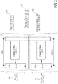
- Figure 3 is one example dataflow and timing diagram 300 of a critical path delay 302 in a stack partitioned power-domain design.
- the current consumed from the power supply is the maximum current of either power-domain (i.e. MAX of either Itop or Ibottom or MAX of either IA or IB).
- power-domain top 304" is the same as “power-domain A” and “power-domain bottom 306" is the same as “power-domain B”.
- Voltage VDD-top 308 is assigned to power-domain top 304 and voltage VDD-bottom 310 is assigned to power-domain bottom 306.
- a set of level-shifters 312 interface signals transiting between the top and bottom power-domains.
- one example of power consumption optimization is based on minimizing the maximum value of Itop and Ibottom.
- Figure 4 is a first example set of instructions for enabling power-domain optimization.
- Tcritical and Itotal are minimized for either a flat or stacked power-domain design using nominal voltage scaling .
- the circuit is partitioned into a set of power-domains. This is part of the design phase (i.e. the design exploration phase), whereby an initial set of locations for the voltage level-shifters (LS) is chosen.
- the design phase i.e. the design exploration phase
- LS voltage level-shifters
- the level-shifters are located at the boundary of specific IP-blocks and/or subsystems, (e.g. at a boundary between a high speed subsystem and a low speed subsystem).
- the boundaries can be located between a memory subsystem, which operates at a lower voltage, and a CPU or other logic subsystem which operates at a higher voltage or vice-versa (Generally, memory is at higher voltage than logic/CPU, since memory voltages do not scale as much as logic voltages).
- a technique for minimizing timing and current overhead associated with such level-shifters is by minimizing the number of level-shifter-cells.
- an initial set of nominal power supply voltages for the set of power-domains is selected.
- a circuit profiler e.g. circuit logic, a microcontroller or a computer computes Tcritical, Itotal, IA (power-domain A current) and IB (power-domain B current) are computed.
- this computation is done using a set of infrastructure components (e.g. libraries containing timing and power information).
- infrastructure components e.g. libraries containing timing and power information.
- the financial costs for generation and supporting such infrastructure components are significant and certain support teams and additional tools are required.
- the infrastructure components supported may be limited to only a few power-domain voltages (e.g. VDDA and VDDB), and circuit design closure may require additional manual input from a design team.
- the computation described in 406 is performed using this different set of nominal power supply voltages. These newer (i.e. instruction 410) set of computations are then compared with the prior (i.e. instruction 406) set of computations.
- a final set of nominal power supply voltages are assigned to the set of power-domains.
- Figure 5 is a second example list of instructions for enabling power-domain optimization.
- Tcritical and Itotal are minimized for either a flat or stacked power-domain design using variable partitioning (i.e. changing locations of one or more signal level-shifters) and nominal voltage scaling .
- Instructions 502, 504, 506, 508 and 510 are similar to instructions 402, 404, 406, 408 and 410 discussed earlier.
- level-shifters are logically moved using EDA design tools to such other location and instructions 504, 506, 508 and 510 are repeated.
- the set of level-shifter positions corresponding to either a lowest total circuit power consumption, a lowest Tcritical, or some combination of both is selected.
- a final set of nominal power supply voltages are assigned to the set of power-domains corresponding to the selected set of level-shifter positions.
- Example instances of this design methodology also rely on the infrastructure components limitations mentioned earlier and are subject to similar limitations. Also, in some examples, this design methodology may only optimize the power consumption within individual power-domains instead of for the entire circuit. For example, in some instances these techniques will either scale the voltage of all power-domains equally or scale only one of the power-domains.
- Figure 6 is a third example list of instructions for enabling power-domain optimization.
- Tcritical and Itotal are minimized for either a flat or a stacked power-domain design using variable partitioning and both nominal and real-time voltage scaling.
- these algorithms can be applied both during both the design phase as well as during the real-time dynamic operational phase.
- Eqns. 6 and 7 are used to represent delay and current consumption in a digital system.
- Delay T K * VDD / VDD ⁇ Vth ⁇
- Vth is threshold voltage
- K is a proportionality constant
- 'a' is velocity saturation index (1 ⁇ a ⁇ 2).
- I a * C * VDD * f
- 'a' is the average number of output transitions in each clock period. It is usually less than 1, and so is often also defined as the probability of an output transition in a clock period; f is the clock frequency; C is the load capacitance. This can be extended for SOC where, 'a' is related with the average switching activity; C is total intrinsic capacitance of digital (switching part e.g. CPU). Eqn. 7 can be derived by dividing the power dissipation with voltage and merge 1 ⁇ 2 also into 'a'.
- Tcritical ml * VDDA / VDDA ⁇ Vth ⁇ + m 2 * VDDB / VDDA ⁇ Vth ⁇
- m1 TA * VDDA ⁇ Vth ⁇ / VDDA
- m 2 TB * VDDB ⁇ Vth ⁇ / VDDB
- k1, k2 are proportionality constants based on the circuit design and an assumption that each power-domain will operate at fixed frequency.
- k 1 IA / VDDA
- k 2 IB / VDDB
- Eqns. 8 and 11 are used to optimize overall system performance, during either the design phase or the real-time operational phase, and use fewer computational resources and fewer or none of the infrastructure components than the approach described in Figures 4 and 5 .
- the circuit is partitioned into an initial set of power-domains. This is part of the design phase.
- an initial set of nominal power supply voltages for the set of power-domains is selected by a circuit controller (e.g. circuit logic, a microcontroller or a computer).
- a circuit controller e.g. circuit logic, a microcontroller or a computer.
- a circuit profiler e.g. circuit logic, a microcontroller or a computer estimates or computes values for the operating parameters Tcritical, Itotal, IA (first power-domain (e.g. A) current) and IB (second power-domain (e.g. B) current).
- Tcritical TA + TB, where TA is the delay time for the first power-domain and TB is the delay time for the second power-domain.
- the operating parameter values are computed as discussed instruction 406 of Figure 4 .
- the estimate may require inserting few different VDDs to create linear equations. If the available infrastructure (like timing libraries not available then another alternative is to just compute (simulation of critical path or refer to design timing reports generated by the EDA tools.
- the values of at least one of the operating parameter are incrementally swept over a range of voltages (e.g. 0V up to the first power-domain's maximum operational voltage) using the circuit controller.
- operational parameter values for TA, TB, Tcritical, IA, IB, Itotal, and VDDB are derived using the circuit profiler. Note, during the design phase these parameter values are computed using Eqns. 8 through 13 using simulated versions of both power-domains. However during the operational phase these parameter values are derived in real-time using Eqns. 8 through 13 using actual measured signal values from both power-domain's actual hardware circuits.
- each set of operational parameter values are then compared with the prior set of operational parameter values. Iterations between instructions 608 and 612 are performed until the circuit is optimized by either minimizing total circuit power consumption (i.e. Itotal), minimizing Tcritical, or minimizing some combination of both.
- Tcritical, Itotal, IA and IB are validated so that the loop does not iterate infinitely. However in example embodiments, iteration is continued if the resulting power consumption is less than the previous one. When power consumption starts increasing, a few (e.g. three) more iterations can be performed to filter out the effect of noise, and ensure that the minima is reached in a reliable manner.
- the EDA design software checks whether there is another possible set of level-shifter (LS) locations.
- LS level-shifter
- level-shifters are logically moved using EDA design tools to such other location and instructions 604, 606, 608, 610 and 612 are repeated.
- a final set of nominal power supply voltages are assigned to the set of power-domains corresponding to the selected set of level-shifter positions by the circuit controller.
- Figures 7A, 7B and 7C show a first example set of EDA design simulation results for flat and stacked power-domain circuits.
- VDDA0 Power-Domain-A's voltage
- Figure 7A shows an example graph of the effect of a VDDA voltage sweep on both power-domain's timing delay (i.e. TA, TB).
- Figure 7B shows an example graph of the effect of a VDDA voltage sweep on power-domain B's voltage (VDDB).
- Figure 7C shows an example graph of the effect of a VDDA voltage sweep on the current consumption (Itotal) for both a flat and stacked set of power-domains.
- Itotal current consumption
- Figure 7C clear minimums in the total current consumption curves, for a given Ttotal, are visible.
- Figures 8A, 8B and 8C show a second example set of EDA design simulation results for flat and stacked power-domain circuits.
- VDDA0 Power-Domain-A's voltage
- Figure 8A shows an example graph of the effect of a VDDA voltage sweep on both power-domain's timing delay (i.e. TA, TB).
- Figure 8B shows an example graph of the effect of a VDDA voltage sweep on power-domain B's voltage (VDDB).
- Figure 8C shows an example graph of the effect of a VDDA voltage sweep on the current consumption (Itotal) for both a flat and stacked set of power-domains. Again, in Figure 8C , clear minimums in the total current consumption curves, for a given Ttotal, are visible.
- VDDA should initially be about 0.7V and VDDB be about 1V, for either flat or stacked power-domain circuit designs.
- VDDA voltage sweeping routine may be used to characterize the circuit and similarly select specific VDDA and VDDB values in real-time response to changes in each power-domain's task/logic/software loading.
- Such voltage scaling adaptation functionality during design-time and run-time, optimally maintains low power consumption in the circuit.
- the overall circuit design is cleanly partitioned such that the level-shifters remain within their operating limits (e.g. power consumption and silicon area overhead) and such each power-domain has similar power consumption requirements for range of task, logic or software applications.
- the level-shifters remain within their operating limits (e.g. power consumption and silicon area overhead) and such each power-domain has similar power consumption requirements for range of task, logic or software applications.
- level-shifting is either not required or very minimally required.
- level-shifters are required.
- a well chosen set of power-domain partitions simplifies overhead calculations performed during the real-time operational phase of power-domain optimization.
- the partitioning creates a set of power-domains having different power consumption levels.
- a generic microcontroller design consumes more power in the CPU power-domain during dynamic operations, while in standby mode, the memory power-domain consumes more power, since most of the CPU logic can be powered-off.
- a memory consumes about 30-40% power while microcontroller logic consumes 60-70% of the power, when both power-domains are operating at the same voltage (e.g. 1 V for 40nm technology).
- critical path delay can be between the CPU and the SRAM, where, logic is responsible for 30-40% of critical delay and memory is 60-70%. For example, for a 100MHz MCU design (10ns timing/clock period) and with memory speed ( ⁇ 130MHz in C40).
- VDDA for the CPU/MCU/logic is reduced, while the SRAM/memory is kept at 1V. This causes the CPU/MCU/logic timing delay to increase but does reduce power consumption. So as not to make the overall circuit design slower, VDDB for the SRAM/memory power-domain is increased, which reduces timing delay in the SRAM/memory power-domain.
- Figure 9 is example system 900 for hosting instructions for enabling a power-domain optimization apparatus.
- the system 900 shows an input/output data 902 interface with a computing device 904 (e.g. a controller).
- the computing device 904 includes a processor device 906, a storage device 908, and a machine-readable storage medium 910. Instructions 912 within the machine-readable storage medium 910 control how the processor 906 interprets and transforms the input data 902, using data within the storage device 908.
- the machine-readable storage medium in an alternate example embodiment is a computer-readable storage medium.
- FIG. 910 Various example sets of instructions stored in the machine-readable storage medium 910 include those shown in Figures 4 , 5 and 6 .
- the processor (such as a central processing unit, CPU, microprocessor, application-specific integrated circuit (ASIC), etc.) controls the overall operation of the storage device (such as random access memory (RAM) for temporary data storage, read only memory (ROM) for permanent data storage, firmware, flash memory, external and internal hard-disk drives, and the like).
- the processor device communicates with the storage device and non-transient machine-readable storage medium using a bus and performs operations and tasks that implement one or more instructions stored in the machine-readable storage medium.
- the machine-readable storage medium in an alternate example embodiment is a computer-readable storage medium.
- the set of instructions described above are implemented as functional and software instructions embodied as a set of executable instructions in a non-transient computer-readable or computer-usable media which are effected on a computer or machine programmed with and controlled by said executable instructions.
- Said instructions are loaded for execution on a processor (such as one or more CPUs).
- Said processor includes microprocessors, microcontrollers, processor modules or subsystems (including one or more microprocessors or microcontrollers), or other control or computing devices.
- a processor can refer to a single component or to plural components.
- Said computer-readable or computer-usable storage medium or media is (are) considered to be part of an article (or article of manufacture).
- An article or article of manufacture can refer to any manufactured single component or multiple components.
- the non-transient machine or computer-usable media or mediums as defined herein excludes signals, but such media or mediums may be capable of receiving and processing information from signals and/or other transient mediums.
- Example embodiments of the material discussed in this specification can be implemented in whole or in part through network, computer, or data based devices and/or services. These may include cloud, internet, intranet, mobile, desktop, processor, look-up table, microcontroller, consumer equipment, infrastructure, or other enabling devices and services. As may be used herein and in the claims, the following non-exclusive definitions are provided.
- one or more instructions or steps discussed herein are automated.
- the terms automated or automatically mean controlled operation of an apparatus, system, and/or process using computers and/or mechanical/electrical devices without the necessity of human intervention, observation, effort and/or decision.
Abstract
Description
- The specification herein incorporates by reference a to be published
U.S. Patent Application Serial No. 14973575 filed on December 17, 2015 - The present specification relates to systems, methods, apparatuses, devices, articles of manufacture and instructions for power management.
- Circuit designs can often be partitioned into multiple power-domains. Depending upon the partitioning, either flat power-domains having multiple supply voltages (MSV) or stacked power-domains employing charge recycling can be created.
- Partitioning and assigning voltages to each of these power-domains however can be a complex, costly and time consuming process, requiring extensive infrastructure support.
- Power consumption of such partitioned circuits is often not optimal and can drain batteries and/or unnecessarily increase electrical consumption.
- According to an example embodiment, an apparatus for power management, comprising: a circuit having a first power-domain and a second power-domain; wherein the first and second power-domains include a set of operating parameter values; a circuit controller configured to incrementally sweep at least one of the operating parameter values of the first power-domain; and a circuit profiler configured to derive a total power consumption profile of the circuit based on the circuit's response to the swept operating parameter value; wherein the circuit controller sets the operating parameter values for the first and second power-domains based on the total power consumption profile of the circuit.
- In another example embodiment, the set of operating parameters include at least one of: an operating voltage, an operating current, an operating delay time, an operating frequency or an operating task.
- In another example embodiment, the circuit controller sets the operating voltage values for the first and second power-domains to minimize at least one of: a total circuit current, the total power consumption of the circuit or a total circuit delay.
- In another example embodiment, the incremental sweep is performed in real-time during circuit operation.
- In another example embodiment, the power-domains are configured in at least one of: a flat configuration or a stacked configuration.
- In another example embodiment, the circuit controller is an adaptive-relative-voltage-frequency-scaling (ARVFS) controller.
- In another example embodiment, VDDA is an operating voltage and IA is an operating current for the first power-domain; VDDB is an operating voltage and IB is an operating current for the second power-domain; k1=IA/VDDA, k2=IB/VDDB; and the circuit profiler configured to derive the total power consumption profile based on equation: I-total = k1 * VDDA + k2 * VDDB.
- In another example embodiment, the circuit profiler configured to derive a total timing delay profile of the circuit based on the circuit's response to the incremental sweep of the operating parameter value; and the circuit controller also sets the operating parameter values for the first and second power-domains based on the total timing delay profile of the circuit.
- In another example embodiment, VDDA is an operating voltage for the first power-domain, and VDDB is an operating voltage for the second power-domain; TA is an operating delay time for the first power-domain and TB is an operating delay time for the second power-domain; Vth is a threshold voltage and 'a' is velocity saturation index; m1 = TA * (VDDA - Vth)a/ VDDA, and m2= TB * (VDDB - Vth)a/ VDDB; and the circuit profiler configured to derive the total timing delay profile based on equation: Tcritical = ml *VDDA/(VDDA - Vth)a + m2*VDDB/( VDDB - Vth)a.
- In another example embodiment, further comprising a set of level-shifters for translating a set of signals exchanged between the first power-domain and the second power-domain; the circuit controller positions the level-shifters at a first set of locations in the circuit; the circuit profiler is configured to derive a first total power consumption profile of the circuit with the set of level-shifters positioned at the first set of locations; the circuit controller positions the level-shifters at a second set of locations in the circuit; the circuit profiler is configured to derive a second total power consumption profile of the circuit with the set of level-shifters positioned at the second set of locations; and the circuit controller the set of level-shifter locations based on the total power consumption profile of the circuit.
- In another example embodiment, the circuit controller the set of level-shifter locations such that the total power consumption of the circuit is minimized.
- According to another example embodiment, a method for power management in a circuit having a first power-domain and a second power-domain, wherein the first and second power-domains include a set of operating parameter values, the method comprising: incrementally sweep at least one of the operating parameter values of the first power-domain; deriving a total power consumption profile of the circuit based on the circuit's response to the swept operating parameter value; and setting the operating parameter values for the first and second power-domains based on the total power consumption profile of the circuit.
- According to yet another example embodiment, an article of manufacture includes at least one non-transitory, tangible machine readable storage medium containing executable machine instructions for power management, comprising: wherein the article includes, a circuit having a first power-domain and a second power-domain; wherein the first and second power-domains include a set of operating parameter values; wherein the instructions include, incrementally sweep at least one of the operating parameter values of the first power-domain; deriving a total power consumption profile of the circuit based on the circuit's response to the swept operating parameter value; and setting the operating parameter values for the first and second power-domains based on the total power consumption profile of the circuit.
- The above discussion is not intended to represent every example embodiment or every implementation within the scope of the current or future Claim sets. The Figures and Detailed Description that follow also exemplify various example embodiments.
- Various example embodiments may be more completely understood in consideration of the following Detailed Description in connection with the accompanying Drawings, in which:
-
-
Figure 1 is one example of a dataflow and timing diagram of a critical path delay in a circuit design with or without power-domain partitioning. -
Figure 2 is one example dataflow and timing diagram of a critical path delay in a flat partitioned power-domain design. -
Figure 3 is one example dataflow and timing diagram of a critical path delay in a stack partitioned power-domain design. -
Figure 4 : is first example set of instructions for enabling power-domain optimization. -
Figure 5 : is second example set of instructions for enabling power-domain optimization. -
Figure 6 : is third example set of instructions for enabling power-domain optimization. -
Figures 7A, 7B and 7C show a first example set of EDA design simulation results for flat and stacked power-domain circuits. -
Figures 8A, 8B and 8C show a second example set of EDA design simulation results for flat and stacked power-domain circuits. -
Figure 9 is an example system for hosting instructions for enabling a power-domain optimization apparatus. - While the disclosure is amenable to various modifications and alternative forms, specifics thereof have been shown by way of example in the drawings and will be described in detail. It should be understood, however, that other embodiments, beyond the particular embodiments described, are possible as well. All modifications, equivalents, and alternative embodiments falling within the spirit and scope of the appended claims are covered as well.
- Herein discussed are design and control techniques for partitioning circuit designs into multiple power-domains and then assigning both nominal and real-time voltages to each of such power-domains.
- These techniques can be applied to any number of flat or stacked power-domains, or some combination of flat and stacked power-domains.
- The techniques discussed below can be applied both at the design phase and during the dynamic real-time operational circuit control phase. Techniques at design phase can also be incorporated into design flow and algorithms for EDA tools.
- During the design phase (i.e. initial design optimization) optimal partitioning of the power-domains (i.e. positioning of the inter-domain signal level-shifters), and optimal assignment of nominal power-domain voltages is performed.
- During the real-time operational phase optimal dynamic power-domain voltage assignments are made using a software or embedded hardware controller for voltage, frequency and/or task scaling Tasks are herein defined to include a set of logical operations, a set of software instructions, or other activities performed by at least one of the power-domains. In one example embodiment, the controller is an adaptive-relative-voltage-frequency-scaling (ARVFS) controller.
- In one example embodiment, the operational phase optimization techniques are embedded in hardware, while in another example embodiment these techniques are implemented using computerized software. Dynamic Voltage and Frequency Scaling (DVFS) techniques may be used in other example embodiments.
- While the discussion below is presented with respect to voltage assignments for multiple power-domains, the optimization algorithms can also be extended to tune the substrate biasing in design and applications.
-
Figure 1 is one example dataflow and timing diagram 100 of a critical path delay 102 (i.e. Tcritical) in a circuit design with or without power-domain partitioning. - The speed of a digital circuit design is characterized by its register-to-register delay (i.e. critical path delay 102). Tcritical 102 is determined by the speed at which data can be transferred between two registers/flip-
flops combinational logic 108 between the registers/flip-flops -
Figure 2 is one example dataflow and timing diagram 200 of a critical path delay 202 (i.e. Tcritical) in a multiple supply voltage (MSV) partitioned power-domain design (also called flat design from here onwards in this document). In this example with multiple supply voltage (MSV) (i.e. flat) design, the Tcritical path crosses two power domains (e.g. power-domain A 204 and power-domain B 206). Each power-domain has its own voltage rails (i.e. VDDA 208 and VDDB 210). - When the power-domain's voltage levels (VDDA, VDDB) are different, circuit signals transmitted between the two power-domains need to be translated (i.e. level-shifted) using signal voltage level-
shifters 212. - Here assuming that such level-
shifters 212 have negligible overhead timing delay and power requirements as compared to the overall flat design, then:
- Total current (Itotal) consumed in this flat power-domain design equals a sum of currents consumed in each power-domain A and B.

- Thus for a flat power-domain design, power consumption optimization is based on the total current consumed by the power-domain A and power-domain A (i.e. IA + IB).
-
Figure 3 is one example dataflow and timing diagram 300 of acritical path delay 302 in a stack partitioned power-domain design. - In a stacked power-domain design, the current consumed from the power supply is the maximum current of either power-domain (i.e. MAX of either Itop or Ibottom or MAX of either IA or IB).
- For the purposes of this discussion "power-
domain top 304" is the same as "power-domain A" and "power-domain bottom 306" is the same as "power-domain B". Voltage VDD-top 308 is assigned to power-domain top 304 and voltage VDD-bottom 310 is assigned to power-domain bottom 306. A set of level-shifters 312 interface signals transiting between the top and bottom power-domains. - For the stacked power-domain design, one example of power consumption optimization is based on minimizing the maximum value of Itop and Ibottom.
- Thus, Eqns. 1 and 2 are rewritten as follows:


-
Figure 4 : is a first example set of instructions for enabling power-domain optimization. In this first example, Tcritical and Itotal are minimized for either a flat or stacked power-domain design using nominal voltage scaling. - The order in which the instructions are discussed does not limit the order in which other example embodiments implement the instructions unless otherwise specifically stated. Additionally, in some embodiments the instructions are implemented in parallel.
- In 402, the circuit is partitioned into a set of power-domains. This is part of the design phase (i.e. the design exploration phase), whereby an initial set of locations for the voltage level-shifters (LS) is chosen.
- In one example, the level-shifters are located at the boundary of specific IP-blocks and/or subsystems, (e.g. at a boundary between a high speed subsystem and a low speed subsystem).
- In an example MCU based design, the boundaries can be located between a memory subsystem, which operates at a lower voltage, and a CPU or other logic subsystem which operates at a higher voltage or vice-versa (Generally, memory is at higher voltage than logic/CPU, since memory voltages do not scale as much as logic voltages).
- A technique for minimizing timing and current overhead associated with such level-shifters is by minimizing the number of level-shifter-cells.
- In 404, an initial set of nominal power supply voltages for the set of power-domains is selected.
- In 406, a circuit profiler (e.g. circuit logic, a microcontroller or a computer) computes Tcritical, Itotal, IA (power-domain A current) and IB (power-domain B current) are computed. In one example, this computation is done using a set of infrastructure components (e.g. libraries containing timing and power information). In some instances, the financial costs for generation and supporting such infrastructure components are significant and certain support teams and additional tools are required. Depending upon these libraries, the infrastructure components supported may be limited to only a few power-domain voltages (e.g. VDDA and VDDB), and circuit design closure may require additional manual input from a design team.
- In 408, a different set of nominal power supply voltages for the set of power-domains is selected.
- In 410, the computation described in 406 is performed using this different set of nominal power supply voltages. These newer (i.e. instruction 410) set of computations are then compared with the prior (i.e. instruction 406) set of computations.
- Iterations between
instructions 

- In 412, a final set of nominal power supply voltages are assigned to the set of power-domains.
-
Figure 5 : is a second example list of instructions for enabling power-domain optimization. In this second example, Tcritical and Itotal are minimized for either a flat or stacked power-domain design using variable partitioning (i.e. changing locations of one or more signal level-shifters) and nominal voltage scaling. - The order in which the instructions are discussed does not limit the order in which other example embodiments implement the instructions unless otherwise specifically stated. Additionally, in some embodiments the instructions are implemented in parallel.
-
Instructions instructions - Next in 512, a check is made whether there is another possible set of level-shifter (LS) locations.
- If another set of level-shifter locations is possible, in 514 the level-shifters are logically moved using EDA design tools to such other location and
instructions - In 512 if there are no other possible set of level-shifter locations, then in 516 the set of level-shifter positions corresponding to either a lowest total circuit power consumption, a lowest Tcritical, or some combination of both is selected.
- In 518 a final set of nominal power supply voltages are assigned to the set of power-domains corresponding to the selected set of level-shifter positions.
- Example instances of this design methodology also rely on the infrastructure components limitations mentioned earlier and are subject to similar limitations. Also, in some examples, this design methodology may only optimize the power consumption within individual power-domains instead of for the entire circuit. For example, in some instances these techniques will either scale the voltage of all power-domains equally or scale only one of the power-domains.
-
Figure 6 : is a third example list of instructions for enabling power-domain optimization. In this third example, Tcritical and Itotal are minimized for either a flat or a stacked power-domain design using variable partitioning and both nominal and real-time voltage scaling. Thus these algorithms can be applied both during both the design phase as well as during the real-time dynamic operational phase. - The order in which the instructions are discussed does not limit the order in which other example embodiments implement the instructions unless otherwise specifically stated. Additionally, in some embodiments the instructions are implemented in parallel.
- Unlike the infrastructure components (e.g. libraries containing timing and power information) used in
Figure 4 andFigure 5 above, an alternative simpler and faster approach to estimating/computing Tcritical, Itotal, IA and IB is now presented. This simpler and faster approach enables real-time voltage scaling in response to dynamic changes as the circuit operates. - To start, Eqns. 6 and 7 are used to represent delay and current consumption in a digital system.

- In Eqn 6, "Vth" is threshold voltage, "K" is a proportionality constant and 'a' is velocity saturation index (1< a<2). For <90nm, a→1-1.3

- In Eqn 7, 'a' : activity, 'C' : intrinsic capacitance, 'VDD': Voltage and 'f' : frequency. Note, Vth is threshold voltage, 90nm refers to CMOS technology (i.e. gate length). Dynamic power (e.g. switching power) is a power dissipated while charging and discharging the capacitive load at the outputs of each CMOS logic cell whenever a transition occurs. Historically, the dynamic power has been a dominant component of power dissipation, expressed as:

- Where, 'a' is the average number of output transitions in each clock period. It is usually less than 1, and so is often also defined as the probability of an output transition in a clock period; f is the clock frequency; C is the load capacitance. This can be extended for SOC where, 'a' is related with the average switching activity; C is total intrinsic capacitance of digital (switching part e.g. CPU). Eqn. 7 can be derived by dividing the power dissipation with voltage and merge ½ also into 'a'.
- Based on the above equations, Tcritical can be written as Eqns. 8.

- In Eqn 8, m1, m2 are proportionality constants based on design realization.


- Based on the above equations, Itotal can be written as Eqns. 11.

- In Eqn 11, k1, k2 are proportionality constants based on the circuit design and an assumption that each power-domain will operate at fixed frequency.


- Eqns. 8 and 11 are used to optimize overall system performance, during either the design phase or the real-time operational phase, and use fewer computational resources and fewer or none of the infrastructure components than the approach described in
Figures 4 and5 . - In 602, the circuit is partitioned into an initial set of power-domains. This is part of the design phase.
- In 604, an initial set of nominal power supply voltages for the set of power-domains is selected by a circuit controller (e.g. circuit logic, a microcontroller or a computer).
- In 606, a circuit profiler (e.g. circuit logic, a microcontroller or a computer) estimates or computes values for the operating parameters Tcritical, Itotal, IA (first power-domain (e.g. A) current) and IB (second power-domain (e.g. B) current). Note, Tcritical = TA + TB, where TA is the delay time for the first power-domain and TB is the delay time for the second power-domain.
- The operating parameters can be estimated using Eqns. 8 through 13 above. Such an estimate is acceptable since in one example only proportionally reliable numbers are necessary for computing the initial system parameters. For example, an estimate such as TA= 0.6* Tcritical and IA=0.3*Itotal at an initial value of VDDA, VDDB is acceptable.
- If an estimate is not possible, then the operating parameter values are computed as discussed
instruction 406 ofFigure 4 . The estimate may require inserting few different VDDs to create linear equations. If the available infrastructure (like timing libraries not available then another alternative is to just compute (simulation of critical path or refer to design timing reports generated by the EDA tools. - In 608, the values of at least one of the operating parameter (e.g. VDDA of the first power-domain) are incrementally swept over a range of voltages (e.g. 0V up to the first power-domain's maximum operational voltage) using the circuit controller.
- In 610, for each specific incremental VDDA voltage, operational parameter values for TA, TB, Tcritical, IA, IB, Itotal, and VDDB are derived using the circuit profiler. Note, during the design phase these parameter values are computed using Eqns. 8 through 13 using simulated versions of both power-domains. However during the operational phase these parameter values are derived in real-time using Eqns. 8 through 13 using actual measured signal values from both power-domain's actual hardware circuits.
- In response to the VDDA increments, in 612 each set of operational parameter values are then compared with the prior set of operational parameter values. Iterations between
instructions - In 614, Tcritical, Itotal, IA and IB are validated so that the loop does not iterate infinitely. However in example embodiments, iteration is continued if the resulting power consumption is less than the previous one. When power consumption starts increasing, a few (e.g. three) more iterations can be performed to filter out the effect of noise, and ensure that the minima is reached in a reliable manner.
- Next in 616 at the design phase, the EDA design software checks whether there is another possible set of level-shifter (LS) locations.
- If another set of level-shifter locations is possible, in 618 the level-shifters are logically moved using EDA design tools to such other location and
instructions - If in 616 there are no other possible set of level-shifter locations, then in 620 the set of level-shifter positions corresponding to either a lowest total circuit power consumption, a lowest Tcritical, or some combination of both is selected.
- In 622 a final set of nominal power supply voltages are assigned to the set of power-domains corresponding to the selected set of level-shifter positions by the circuit controller.
- Thus in view of the discussion above, by using Eqns. 8 and 11 a less computationally intense and costly approach than that used with infrastructure components (e.g. libraries containing timing and power information) is achieved. Due to this more streamlined approach a wider range of design choices can be tested both during the design phase and implemented in real-time during the operational phase.
-
Figures 7A, 7B and 7C show a first example set of EDA design simulation results for flat and stacked power-domain circuits. In this first example set, the flat or stacked circuit's operating conditions are initialized to as set of currents and voltages (e.g. IA0 =1; IB0=2; VDDA0=0.7; VDDB0= 1; Vth =0.4; TA0=1; and TB0=0.1). - Power-Domain-A's voltage (VDDA0) is then swept from 0V to about 1.7V, while the total delay time of both power-domains is kept constant (i.e. Tcritical=1.1).
-
Figure 7A shows an example graph of the effect of a VDDA voltage sweep on both power-domain's timing delay (i.e. TA, TB). -
Figure 7B shows an example graph of the effect of a VDDA voltage sweep on power-domain B's voltage (VDDB). -
Figure 7C shows an example graph of the effect of a VDDA voltage sweep on the current consumption (Itotal) for both a flat and stacked set of power-domains. InFigure 7C , clear minimums in the total current consumption curves, for a given Ttotal, are visible. Total circuit power consumption can then be derived (i.e. Power=Itotal*VDDtotal). -
Figures 8A, 8B and 8C show a second example set of EDA design simulation results for flat and stacked power-domain circuits. In the second example set, the flat or stacked circuit's operating conditions are initialized to as set of currents and voltages (e.g. IA0 =1; IB0=2; VDDA0=0.7; VDDB0= 1; Vth =0.4; TA0=1; and TB0=0.7). - Power-Domain-A's voltage (VDDA0) is then again swept from 0V to about 1.7V, while the total delay time of both power-domains is kept constant (i.e. Tcritical=1.7).
-
Figure 8A shows an example graph of the effect of a VDDA voltage sweep on both power-domain's timing delay (i.e. TA, TB). -
Figure 8B shows an example graph of the effect of a VDDA voltage sweep on power-domain B's voltage (VDDB). -
Figure 8C shows an example graph of the effect of a VDDA voltage sweep on the current consumption (Itotal) for both a flat and stacked set of power-domains. Again, inFigure 8C , clear minimums in the total current consumption curves, for a given Ttotal, are visible. - A comparison between
Figures 7 and8 indicate that for both Tcritical and Itotal to be minimized VDDA should initially be about 0.7V and VDDB be about 1V, for either flat or stacked power-domain circuit designs. - During real-time dynamic circuit operation, a similar VDDA voltage sweeping routine may be used to characterize the circuit and similarly select specific VDDA and VDDB values in real-time response to changes in each power-domain's task/logic/software loading. Such voltage scaling adaptation functionality during design-time and run-time, optimally maintains low power consumption in the circuit.
- One example application of the previously presented design phase and operational phase steps is now discussed with respect to a MoTL stacked memory on top of logic design.
- First, the overall circuit design is cleanly partitioned such that the level-shifters remain within their operating limits (e.g. power consumption and silicon area overhead) and such each power-domain has similar power consumption requirements for range of task, logic or software applications.
- Note that if the circuit design is partitioned into power-domains which are non-interacting (i.e. which do not exchange signals), then level-shifting is either not required or very minimally required.
- However, if the circuit design is partitioned into power-domains which are interacting (e.g. such as a MoTL design) then level-shifters are required.
- A well chosen set of power-domain partitions simplifies overhead calculations performed during the real-time operational phase of power-domain optimization.
- Second. The partitioning creates a set of power-domains having different power consumption levels.
- A generic microcontroller design consumes more power in the CPU power-domain during dynamic operations, while in standby mode, the memory power-domain consumes more power, since most of the CPU logic can be powered-off.
- In an example Internet of Things (IOT) circuit design application using a microcontroller unit (MCU), a memory consumes about 30-40% power while microcontroller logic consumes 60-70% of the power, when both power-domains are operating at the same voltage (e.g. 1 V for 40nm technology). At a same time, critical path delay can be between the CPU and the SRAM, where, logic is responsible for 30-40% of critical delay and memory is 60-70%. For example, for a 100MHz MCU design (10ns timing/clock period) and with memory speed (∼130MHz in C40).
- Third. Next VDDA for the CPU/MCU/logic is reduced, while the SRAM/memory is kept at 1V. This causes the CPU/MCU/logic timing delay to increase but does reduce power consumption. So as not to make the overall circuit design slower, VDDB for the SRAM/memory power-domain is increased, which reduces timing delay in the SRAM/memory power-domain.
- While the examples above have described a voltage scaling application, similar techniques can be applied to substrate biasing.
-
Figure 9 isexample system 900 for hosting instructions for enabling a power-domain optimization apparatus. Thesystem 900 shows an input/output data 902 interface with a computing device 904 (e.g. a controller). Thecomputing device 904 includes aprocessor device 906, astorage device 908, and a machine-readable storage medium 910.Instructions 912 within the machine-readable storage medium 910 control how theprocessor 906 interprets and transforms theinput data 902, using data within thestorage device 908. The machine-readable storage medium in an alternate example embodiment is a computer-readable storage medium. - Various example sets of instructions stored in the machine-
readable storage medium 910 include those shown inFigures 4 ,5 and6 . - The processor (such as a central processing unit, CPU, microprocessor, application-specific integrated circuit (ASIC), etc.) controls the overall operation of the storage device (such as random access memory (RAM) for temporary data storage, read only memory (ROM) for permanent data storage, firmware, flash memory, external and internal hard-disk drives, and the like). The processor device communicates with the storage device and non-transient machine-readable storage medium using a bus and performs operations and tasks that implement one or more instructions stored in the machine-readable storage medium. The machine-readable storage medium in an alternate example embodiment is a computer-readable storage medium.
- The instructions and/or flowchart steps in the above Figures can be executed in any order, unless a specific order is explicitly stated. Also, those skilled in the art will recognize that while one example set of instructions/method has been discussed, the material in this specification can be combined in a variety of ways to yield other examples as well, and are to be understood within a context provided by this detailed description.
- In some example embodiments the set of instructions described above are implemented as functional and software instructions embodied as a set of executable instructions in a non-transient computer-readable or computer-usable media which are effected on a computer or machine programmed with and controlled by said executable instructions. Said instructions are loaded for execution on a processor (such as one or more CPUs). Said processor includes microprocessors, microcontrollers, processor modules or subsystems (including one or more microprocessors or microcontrollers), or other control or computing devices. A processor can refer to a single component or to plural components. Said computer-readable or computer-usable storage medium or media is (are) considered to be part of an article (or article of manufacture). An article or article of manufacture can refer to any manufactured single component or multiple components. The non-transient machine or computer-usable media or mediums as defined herein excludes signals, but such media or mediums may be capable of receiving and processing information from signals and/or other transient mediums.
- Example embodiments of the material discussed in this specification can be implemented in whole or in part through network, computer, or data based devices and/or services. These may include cloud, internet, intranet, mobile, desktop, processor, look-up table, microcontroller, consumer equipment, infrastructure, or other enabling devices and services. As may be used herein and in the claims, the following non-exclusive definitions are provided.
- In one example, one or more instructions or steps discussed herein are automated. The terms automated or automatically (and like variations thereof) mean controlled operation of an apparatus, system, and/or process using computers and/or mechanical/electrical devices without the necessity of human intervention, observation, effort and/or decision.
- In this specification, example embodiments have been presented in terms of a selected set of details. However, a person of ordinary skill in the art would understand that many other example embodiments may be practiced which include a different selected set of these details. It is intended that the following claims cover all possible example embodiments.
Claims (13)
- An apparatus for power management, comprising:a circuit having a first power-domain and a second power-domain;wherein the first and second power-domains include a set of operating parameter values;a circuit controller configured to incrementally sweep at least one of the operating parameter values of the first power-domain; anda circuit profiler configured to derive a total power consumption profile of the circuit based on the circuit's response to the swept operating parameter value;wherein the circuit controller sets the operating parameter values for the first and second power-domains based on the total power consumption profile of the circuit.
- The apparatus of claim 1:wherein the set of operating parameters include at least one of: an operating voltage, an operating current, an operating delay time, an operating frequency or an operating task.
- The apparatus of claim 2:wherein the circuit controller sets the operating voltage values for the first and second power-domains to minimize at least one of: a total circuit current, the total power consumption of the circuit or a total circuit delay.
- The apparatus of claim 1:wherein the incremental sweep is performed in real-time during circuit operation.
- The apparatus of claim 1:wherein the power-domains are configured in at least one of: a flat configuration or a stacked configuration.
- The apparatus of claim 1:wherein the circuit controller is an adaptive-relative-voltage-frequency-scaling (ARVFS) controller.
- The apparatus of claim 1:wherein VDDA is an operating voltage and IA is an operating current for the first power-domain;wherein VDDB is an operating voltage and IB is an operating current for the second power-domain;wherein k1=IA/VDDA, k2=IB/VDDB; andwherein the circuit profiler configured to derive the total power consumption profile based on equation: 1-total = k1 * VDDA + k2 * VDDB.
- The apparatus of claim 1:wherein the circuit profiler configured to derive a total timing delay profile of the circuit based on the circuit's response to the incremental sweep of the operating parameter value; andwherein the circuit controller also sets the operating parameter values for the first and second power-domains based on the total timing delay profile of the circuit.
- The apparatus of claim 8:wherein VDDA is an operating voltage for the first power-domain, and VDDB is an operating voltage for the second power-domain;wherein TA is an operating delay time for the first power-domain and TB is an operating delay time for the second power-domain;wherein Vth is a threshold voltage and 'a' is velocity saturation index;wherein m1 = TA * (VDDA - Vth)a/ VDDA, and m2= TB * (VDDB - Vth)a/ VDDB; andwherein the circuit profiler configured to derive the total timing delay profile based on equation: Tcritical = m1 *VDDA/(VDDA - Vth)a + m2*VDDB/( VDDB - Vth)a.
- The apparatus of claim 1:further comprising a set of level-shifters for translating a set of signals exchanged between the first power-domain and the second power-domain;wherein the circuit controller positions the level-shifters at a first set of locations in the circuit;wherein the circuit profiler is configured to derive a first total power consumption profile of the circuit with the set of level-shifters positioned at the first set of locations;wherein the circuit controller positions the level-shifters at a second set of locations in the circuit;wherein the circuit profiler is configured to derive a second total power consumption profile of the circuit with the set of level-shifters positioned at the second set of locations; andwherein the circuit controller the set of level-shifter locations based on the total power consumption profile of the circuit.
- The apparatus of claim 10:wherein the circuit controller the set of level-shifter locations such that the total power consumption of the circuit is minimized.
- A method for power management in a circuit having a first power-domain and a second power-domain, wherein the first and second power-domains include a set of operating parameter values, the method comprising:incrementally sweep at least one of the operating parameter values of the first power-domain;deriving a total power consumption profile of the circuit based on the circuit's response to the swept operating parameter value; andsetting the operating parameter values for the first and second power-domains based on the total power consumption profile of the circuit.
- An article of manufacture including at least one non-transitory, tangible machine readable storage medium containing executable machine instructions for power management, comprising:wherein the article includes,a circuit having a first power-domain and a second power-domain;wherein the first and second power-domains include a set of operating parameter values;wherein the instructions include,incrementally sweep at least one of the operating parameter values of the first power-domain;deriving a total power consumption profile of the circuit based on the circuit's response to the swept operating parameter value; andsetting the operating parameter values for the first and second power-domains based on the total power consumption profile of the circuit.
Applications Claiming Priority (1)
| Application Number | Priority Date | Filing Date | Title |
|---|---|---|---|
| US14/973,616 US9960769B2 (en) | 2015-12-17 | 2015-12-17 | Power-domain optimization |
Publications (2)
| Publication Number | Publication Date |
|---|---|
| EP3182249A1 true EP3182249A1 (en) | 2017-06-21 |
| EP3182249B1 EP3182249B1 (en) | 2020-06-17 |
Family
ID=57680071
Family Applications (1)
| Application Number | Title | Priority Date | Filing Date |
|---|---|---|---|
| EP16204356.6A Active EP3182249B1 (en) | 2015-12-17 | 2016-12-15 | Power-domain optimization |
Country Status (3)
| Country | Link |
|---|---|
| US (1) | US9960769B2 (en) |
| EP (1) | EP3182249B1 (en) |
| CN (1) | CN107025322B (en) |
Families Citing this family (4)
| Publication number | Priority date | Publication date | Assignee | Title |
|---|---|---|---|---|
| US10535394B2 (en) | 2017-07-20 | 2020-01-14 | Samsung Electronics Co., Ltd. | Memory device including dynamic voltage and frequency scaling switch and method of operating the same |
| US10664035B2 (en) * | 2017-08-31 | 2020-05-26 | Qualcomm Incorporated | Reconfigurable power delivery networks |
| CN111381654B (en) * | 2018-12-29 | 2022-01-11 | 成都海光集成电路设计有限公司 | Load detection circuit, SOC system, and method for configuring load detection circuit |
| US11455450B1 (en) * | 2021-06-03 | 2022-09-27 | Cadence Design Systems, Inc. | System and method for performing sign-off timing analysis of electronic circuit designs |
Citations (4)
| Publication number | Priority date | Publication date | Assignee | Title |
|---|---|---|---|---|
| US20070011643A1 (en) * | 2003-09-19 | 2007-01-11 | Cadence Design Systems, Inc. | Optimized mapping of an integrated circuit design to multiple cell libraries during a single synthesis pass |
| US7551985B1 (en) * | 2006-10-30 | 2009-06-23 | Cadence Design Systems, Inc. | Method and apparatus for power consumption optimization for integrated circuits |
| US7594208B1 (en) * | 2003-07-22 | 2009-09-22 | Altera Corporation | Techniques for automated sweeping of parameters in computer-aided design to achieve optimum performance and resource usage |
| US20120054511A1 (en) * | 2010-08-31 | 2012-03-01 | Sonics, Inc | Intelligent power controller |
Family Cites Families (17)
| Publication number | Priority date | Publication date | Assignee | Title |
|---|---|---|---|---|
| JP3300593B2 (en) | 1995-06-15 | 2002-07-08 | 株式会社東芝 | Semiconductor integrated circuit device |
| US6479974B2 (en) | 2000-12-28 | 2002-11-12 | International Business Machines Corporation | Stacked voltage rails for low-voltage DC distribution |
| US6759872B2 (en) | 2002-03-14 | 2004-07-06 | Koninklijke Philips Electronics N.V. | I/O circuit with mixed supply voltage capability |
| US7329968B2 (en) | 2003-05-08 | 2008-02-12 | The Trustees Of Columbia University In The City Of New York | Charge-recycling voltage domains for energy-efficient low-voltage operation of digital CMOS circuits |
| US7702929B2 (en) | 2004-11-29 | 2010-04-20 | Marvell World Trade Ltd. | Low voltage logic operation using higher voltage supply levels |
| EP2156269A2 (en) * | 2007-06-04 | 2010-02-24 | Nxp B.V. | Power supply management integrated circuit |
| ES2407504T3 (en) | 2007-08-02 | 2013-06-12 | Emd Millipore Corporation | Sampling system |
| US8200990B2 (en) | 2007-12-22 | 2012-06-12 | International Business Machines Corporation | Apparatus, system, and method for a high efficiency redundant power architecture |
| US7984317B2 (en) | 2008-03-24 | 2011-07-19 | Apple Inc. | Hardware-based power management of functional blocks |
| US8174288B2 (en) | 2009-04-13 | 2012-05-08 | International Business Machines Corporation | Voltage conversion and integrated circuits with stacked voltage domains |
| US8476962B2 (en) | 2009-11-18 | 2013-07-02 | Freescale Semiconductor, Inc. | System having multiple voltage tiers and method therefor |
| US7982498B1 (en) * | 2010-05-18 | 2011-07-19 | Global Unichip Corp. | System and method for power domain isolation |
| US8339177B2 (en) * | 2011-01-26 | 2012-12-25 | Freescale Semiconductor, Inc. | Multiple function power domain level shifter |
| US8558603B2 (en) | 2011-12-15 | 2013-10-15 | Apple Inc. | Multiplexer with level shifter |
| US8984463B2 (en) * | 2012-11-28 | 2015-03-17 | Qualcomm Incorporated | Data transfer across power domains |
| US8878387B1 (en) | 2013-05-16 | 2014-11-04 | Micrel, Inc. | Multi-level stack voltage system for integrated circuits |
| US20150346742A1 (en) | 2014-06-02 | 2015-12-03 | Nxp B.V. | Energy recycling for a cost effective platform to optimize energy efficiency for low powered system |
-
2015
- 2015-12-17 US US14/973,616 patent/US9960769B2/en active Active
-
2016
- 2016-12-15 CN CN201611164288.1A patent/CN107025322B/en active Active
- 2016-12-15 EP EP16204356.6A patent/EP3182249B1/en active Active
Patent Citations (4)
| Publication number | Priority date | Publication date | Assignee | Title |
|---|---|---|---|---|
| US7594208B1 (en) * | 2003-07-22 | 2009-09-22 | Altera Corporation | Techniques for automated sweeping of parameters in computer-aided design to achieve optimum performance and resource usage |
| US20070011643A1 (en) * | 2003-09-19 | 2007-01-11 | Cadence Design Systems, Inc. | Optimized mapping of an integrated circuit design to multiple cell libraries during a single synthesis pass |
| US7551985B1 (en) * | 2006-10-30 | 2009-06-23 | Cadence Design Systems, Inc. | Method and apparatus for power consumption optimization for integrated circuits |
| US20120054511A1 (en) * | 2010-08-31 | 2012-03-01 | Sonics, Inc | Intelligent power controller |
Also Published As
| Publication number | Publication date |
|---|---|
| US9960769B2 (en) | 2018-05-01 |
| EP3182249B1 (en) | 2020-06-17 |
| CN107025322B (en) | 2022-04-15 |
| CN107025322A (en) | 2017-08-08 |
| US20170179957A1 (en) | 2017-06-22 |
Similar Documents
| Publication | Publication Date | Title |
|---|---|---|
| EP3182249B1 (en) | Power-domain optimization | |
| US20160112052A1 (en) | Low Power Automatic Calibration Method for High Frequency Oscillators | |
| US10416746B2 (en) | Adaptive energy optimal computing | |
| US20080301604A1 (en) | Apparatus for and method of estimating the quality of clock gating solutions for integrated circuit design | |
| US7000204B2 (en) | Power estimation based on power characterizations | |
| EP2610702A2 (en) | Power consumption prediction method for clock-gating integrated circuit device | |
| CN106662902B (en) | Multi-domain heterogeneous process-voltage-temperature tracking for integrated circuit power reduction | |
| US20140139262A1 (en) | Multiple threshold voltage standard cells | |
| CN110710107A (en) | Apparatus and method for reducing voltage droop due to clock latch-up | |
| US9958922B2 (en) | Low ripple mechanism of mode change in switched capacitor voltage regulators | |
| WO2021061364A1 (en) | Adaptive on-chip digital power estimator | |
| US8516424B2 (en) | Timing signoff system and method that takes static and dynamic voltage drop into account | |
| US8434048B2 (en) | Method for implementing power gating in an integrated circuit design logic block including N-nary dynamic logic (NDL) gates | |
| US20240047966A1 (en) | Systems, devices and methods for power management and power estimation | |
| US8166319B2 (en) | Methods and systems for use-case aware voltage selection | |
| US8621415B2 (en) | Obtaining power domain by clustering logical blocks based on activation timings | |
| Moghaddam et al. | Investigation of DVFS based dynamic reliability management for chip multiprocessors | |
| US10175734B1 (en) | Techniques for adjusting latency of a clock signal to affect supply voltage | |
| Held | Gate sizing for large cell-based designs | |
| US20140082573A1 (en) | Circuit design support apparatus, circuit design support method, and computer product | |
| Ghasemazar et al. | Optimizing the power-delay product of a linear pipeline by opportunistic time borrowing | |
| Guang et al. | A review of dynamic power management methods in NoC under emerging design considerations | |
| Keller | Energy-efficient system design through adaptive voltage scaling | |
| US10162922B2 (en) | Hybrid clock gating methodology for high performance cores | |
| Tawfik et al. | Clock distribution networks with gradual signal transition time relaxation for reduced power consumption |
Legal Events
| Date | Code | Title | Description |
|---|---|---|---|
| PUAI | Public reference made under article 153(3) epc to a published international application that has entered the european phase |
Free format text: ORIGINAL CODE: 0009012 |
|
| STAA | Information on the status of an ep patent application or granted ep patent |
Free format text: STATUS: THE APPLICATION HAS BEEN PUBLISHED |
|
| AK | Designated contracting states |
Kind code of ref document: A1 Designated state(s): AL AT BE BG CH CY CZ DE DK EE ES FI FR GB GR HR HU IE IS IT LI LT LU LV MC MK MT NL NO PL PT RO RS SE SI SK SM TR |
|
| AX | Request for extension of the european patent |
Extension state: BA ME |
|
| STAA | Information on the status of an ep patent application or granted ep patent |
Free format text: STATUS: REQUEST FOR EXAMINATION WAS MADE |
|
| 17P | Request for examination filed |
Effective date: 20171221 |
|
| RBV | Designated contracting states (corrected) |
Designated state(s): AL AT BE BG CH CY CZ DE DK EE ES FI FR GB GR HR HU IE IS IT LI LT LU LV MC MK MT NL NO PL PT RO RS SE SI SK SM TR |
|
| STAA | Information on the status of an ep patent application or granted ep patent |
Free format text: STATUS: EXAMINATION IS IN PROGRESS |
|
| 17Q | First examination report despatched |
Effective date: 20181106 |
|
| REG | Reference to a national code |
Ref country code: DE Ref legal event code: R079 Ref document number: 602016038149 Country of ref document: DE Free format text: PREVIOUS MAIN CLASS: G06F0001320000 Ipc: G06F0001329600 |
|
| RIC1 | Information provided on ipc code assigned before grant |
Ipc: G06F 1/3296 20190101AFI20191113BHEP Ipc: G06F 11/30 20060101ALI20191113BHEP Ipc: H03K 19/0175 20060101ALI20191113BHEP Ipc: G06F 17/50 20060101ALI20191113BHEP Ipc: G05F 3/02 20060101ALI20191113BHEP |
|
| GRAP | Despatch of communication of intention to grant a patent |
Free format text: ORIGINAL CODE: EPIDOSNIGR1 |
|
| STAA | Information on the status of an ep patent application or granted ep patent |
Free format text: STATUS: GRANT OF PATENT IS INTENDED |
|
| INTG | Intention to grant announced |
Effective date: 20200103 |
|
| RAP1 | Party data changed (applicant data changed or rights of an application transferred) |
Owner name: NXP B.V. |
|
| GRAS | Grant fee paid |
Free format text: ORIGINAL CODE: EPIDOSNIGR3 |
|
| GRAA | (expected) grant |
Free format text: ORIGINAL CODE: 0009210 |
|
| STAA | Information on the status of an ep patent application or granted ep patent |
Free format text: STATUS: THE PATENT HAS BEEN GRANTED |
|
| AK | Designated contracting states |
Kind code of ref document: B1 Designated state(s): AL AT BE BG CH CY CZ DE DK EE ES FI FR GB GR HR HU IE IS IT LI LT LU LV MC MK MT NL NO PL PT RO RS SE SI SK SM TR |
|
| REG | Reference to a national code |
Ref country code: GB Ref legal event code: FG4D |
|
| REG | Reference to a national code |
Ref country code: CH Ref legal event code: EP |
|
| REG | Reference to a national code |
Ref country code: IE Ref legal event code: FG4D |
|
| REG | Reference to a national code |
Ref country code: DE Ref legal event code: R096 Ref document number: 602016038149 Country of ref document: DE |
|
| REG | Reference to a national code |
Ref country code: AT Ref legal event code: REF Ref document number: 1282140 Country of ref document: AT Kind code of ref document: T Effective date: 20200715 |
|
| PG25 | Lapsed in a contracting state [announced via postgrant information from national office to epo] |
Ref country code: NO Free format text: LAPSE BECAUSE OF FAILURE TO SUBMIT A TRANSLATION OF THE DESCRIPTION OR TO PAY THE FEE WITHIN THE PRESCRIBED TIME-LIMIT Effective date: 20200917 Ref country code: GR Free format text: LAPSE BECAUSE OF FAILURE TO SUBMIT A TRANSLATION OF THE DESCRIPTION OR TO PAY THE FEE WITHIN THE PRESCRIBED TIME-LIMIT Effective date: 20200918 Ref country code: FI Free format text: LAPSE BECAUSE OF FAILURE TO SUBMIT A TRANSLATION OF THE DESCRIPTION OR TO PAY THE FEE WITHIN THE PRESCRIBED TIME-LIMIT Effective date: 20200617 Ref country code: LT Free format text: LAPSE BECAUSE OF FAILURE TO SUBMIT A TRANSLATION OF THE DESCRIPTION OR TO PAY THE FEE WITHIN THE PRESCRIBED TIME-LIMIT Effective date: 20200617 Ref country code: SE Free format text: LAPSE BECAUSE OF FAILURE TO SUBMIT A TRANSLATION OF THE DESCRIPTION OR TO PAY THE FEE WITHIN THE PRESCRIBED TIME-LIMIT Effective date: 20200617 |
|
| REG | Reference to a national code |
Ref country code: LT Ref legal event code: MG4D |
|
| REG | Reference to a national code |
Ref country code: NL Ref legal event code: MP Effective date: 20200617 |
|
| PG25 | Lapsed in a contracting state [announced via postgrant information from national office to epo] |
Ref country code: BG Free format text: LAPSE BECAUSE OF FAILURE TO SUBMIT A TRANSLATION OF THE DESCRIPTION OR TO PAY THE FEE WITHIN THE PRESCRIBED TIME-LIMIT Effective date: 20200917 Ref country code: RS Free format text: LAPSE BECAUSE OF FAILURE TO SUBMIT A TRANSLATION OF THE DESCRIPTION OR TO PAY THE FEE WITHIN THE PRESCRIBED TIME-LIMIT Effective date: 20200617 Ref country code: LV Free format text: LAPSE BECAUSE OF FAILURE TO SUBMIT A TRANSLATION OF THE DESCRIPTION OR TO PAY THE FEE WITHIN THE PRESCRIBED TIME-LIMIT Effective date: 20200617 Ref country code: HR Free format text: LAPSE BECAUSE OF FAILURE TO SUBMIT A TRANSLATION OF THE DESCRIPTION OR TO PAY THE FEE WITHIN THE PRESCRIBED TIME-LIMIT Effective date: 20200617 |
|
| REG | Reference to a national code |
Ref country code: AT Ref legal event code: MK05 Ref document number: 1282140 Country of ref document: AT Kind code of ref document: T Effective date: 20200617 |
|
| PG25 | Lapsed in a contracting state [announced via postgrant information from national office to epo] |
Ref country code: AL Free format text: LAPSE BECAUSE OF FAILURE TO SUBMIT A TRANSLATION OF THE DESCRIPTION OR TO PAY THE FEE WITHIN THE PRESCRIBED TIME-LIMIT Effective date: 20200617 Ref country code: NL Free format text: LAPSE BECAUSE OF FAILURE TO SUBMIT A TRANSLATION OF THE DESCRIPTION OR TO PAY THE FEE WITHIN THE PRESCRIBED TIME-LIMIT Effective date: 20200617 |
|
| PG25 | Lapsed in a contracting state [announced via postgrant information from national office to epo] |
Ref country code: IT Free format text: LAPSE BECAUSE OF FAILURE TO SUBMIT A TRANSLATION OF THE DESCRIPTION OR TO PAY THE FEE WITHIN THE PRESCRIBED TIME-LIMIT Effective date: 20200617 Ref country code: SM Free format text: LAPSE BECAUSE OF FAILURE TO SUBMIT A TRANSLATION OF THE DESCRIPTION OR TO PAY THE FEE WITHIN THE PRESCRIBED TIME-LIMIT Effective date: 20200617 Ref country code: EE Free format text: LAPSE BECAUSE OF FAILURE TO SUBMIT A TRANSLATION OF THE DESCRIPTION OR TO PAY THE FEE WITHIN THE PRESCRIBED TIME-LIMIT Effective date: 20200617 Ref country code: AT Free format text: LAPSE BECAUSE OF FAILURE TO SUBMIT A TRANSLATION OF THE DESCRIPTION OR TO PAY THE FEE WITHIN THE PRESCRIBED TIME-LIMIT Effective date: 20200617 Ref country code: ES Free format text: LAPSE BECAUSE OF FAILURE TO SUBMIT A TRANSLATION OF THE DESCRIPTION OR TO PAY THE FEE WITHIN THE PRESCRIBED TIME-LIMIT Effective date: 20200617 Ref country code: PT Free format text: LAPSE BECAUSE OF FAILURE TO SUBMIT A TRANSLATION OF THE DESCRIPTION OR TO PAY THE FEE WITHIN THE PRESCRIBED TIME-LIMIT Effective date: 20201019 Ref country code: CZ Free format text: LAPSE BECAUSE OF FAILURE TO SUBMIT A TRANSLATION OF THE DESCRIPTION OR TO PAY THE FEE WITHIN THE PRESCRIBED TIME-LIMIT Effective date: 20200617 Ref country code: RO Free format text: LAPSE BECAUSE OF FAILURE TO SUBMIT A TRANSLATION OF THE DESCRIPTION OR TO PAY THE FEE WITHIN THE PRESCRIBED TIME-LIMIT Effective date: 20200617 |
|
| PG25 | Lapsed in a contracting state [announced via postgrant information from national office to epo] |
Ref country code: IS Free format text: LAPSE BECAUSE OF FAILURE TO SUBMIT A TRANSLATION OF THE DESCRIPTION OR TO PAY THE FEE WITHIN THE PRESCRIBED TIME-LIMIT Effective date: 20201017 Ref country code: SK Free format text: LAPSE BECAUSE OF FAILURE TO SUBMIT A TRANSLATION OF THE DESCRIPTION OR TO PAY THE FEE WITHIN THE PRESCRIBED TIME-LIMIT Effective date: 20200617 Ref country code: PL Free format text: LAPSE BECAUSE OF FAILURE TO SUBMIT A TRANSLATION OF THE DESCRIPTION OR TO PAY THE FEE WITHIN THE PRESCRIBED TIME-LIMIT Effective date: 20200617 |
|
| REG | Reference to a national code |
Ref country code: DE Ref legal event code: R097 Ref document number: 602016038149 Country of ref document: DE |
|
| PLBE | No opposition filed within time limit |
Free format text: ORIGINAL CODE: 0009261 |
|
| STAA | Information on the status of an ep patent application or granted ep patent |
Free format text: STATUS: NO OPPOSITION FILED WITHIN TIME LIMIT |
|
| PG25 | Lapsed in a contracting state [announced via postgrant information from national office to epo] |
Ref country code: DK Free format text: LAPSE BECAUSE OF FAILURE TO SUBMIT A TRANSLATION OF THE DESCRIPTION OR TO PAY THE FEE WITHIN THE PRESCRIBED TIME-LIMIT Effective date: 20200617 |
|
| 26N | No opposition filed |
Effective date: 20210318 |
|
| PG25 | Lapsed in a contracting state [announced via postgrant information from national office to epo] |
Ref country code: SI Free format text: LAPSE BECAUSE OF FAILURE TO SUBMIT A TRANSLATION OF THE DESCRIPTION OR TO PAY THE FEE WITHIN THE PRESCRIBED TIME-LIMIT Effective date: 20200617 |
|
| REG | Reference to a national code |
Ref country code: CH Ref legal event code: PL |
|
| GBPC | Gb: european patent ceased through non-payment of renewal fee |
Effective date: 20201215 |
|
| PG25 | Lapsed in a contracting state [announced via postgrant information from national office to epo] |
Ref country code: MC Free format text: LAPSE BECAUSE OF FAILURE TO SUBMIT A TRANSLATION OF THE DESCRIPTION OR TO PAY THE FEE WITHIN THE PRESCRIBED TIME-LIMIT Effective date: 20200617 |
|
| REG | Reference to a national code |
Ref country code: BE Ref legal event code: MM Effective date: 20201231 |
|
| PG25 | Lapsed in a contracting state [announced via postgrant information from national office to epo] |
Ref country code: FR Free format text: LAPSE BECAUSE OF NON-PAYMENT OF DUE FEES Effective date: 20201231 Ref country code: LU Free format text: LAPSE BECAUSE OF NON-PAYMENT OF DUE FEES Effective date: 20201215 Ref country code: IE Free format text: LAPSE BECAUSE OF NON-PAYMENT OF DUE FEES Effective date: 20201215 |
|
| PG25 | Lapsed in a contracting state [announced via postgrant information from national office to epo] |
Ref country code: GB Free format text: LAPSE BECAUSE OF NON-PAYMENT OF DUE FEES Effective date: 20201215 Ref country code: LI Free format text: LAPSE BECAUSE OF NON-PAYMENT OF DUE FEES Effective date: 20201231 Ref country code: CH Free format text: LAPSE BECAUSE OF NON-PAYMENT OF DUE FEES Effective date: 20201231 |
|
| PG25 | Lapsed in a contracting state [announced via postgrant information from national office to epo] |
Ref country code: IS Free format text: LAPSE BECAUSE OF FAILURE TO SUBMIT A TRANSLATION OF THE DESCRIPTION OR TO PAY THE FEE WITHIN THE PRESCRIBED TIME-LIMIT Effective date: 20201017 Ref country code: TR Free format text: LAPSE BECAUSE OF FAILURE TO SUBMIT A TRANSLATION OF THE DESCRIPTION OR TO PAY THE FEE WITHIN THE PRESCRIBED TIME-LIMIT Effective date: 20200617 Ref country code: MT Free format text: LAPSE BECAUSE OF FAILURE TO SUBMIT A TRANSLATION OF THE DESCRIPTION OR TO PAY THE FEE WITHIN THE PRESCRIBED TIME-LIMIT Effective date: 20200617 Ref country code: CY Free format text: LAPSE BECAUSE OF FAILURE TO SUBMIT A TRANSLATION OF THE DESCRIPTION OR TO PAY THE FEE WITHIN THE PRESCRIBED TIME-LIMIT Effective date: 20200617 |
|
| PG25 | Lapsed in a contracting state [announced via postgrant information from national office to epo] |
Ref country code: MK Free format text: LAPSE BECAUSE OF FAILURE TO SUBMIT A TRANSLATION OF THE DESCRIPTION OR TO PAY THE FEE WITHIN THE PRESCRIBED TIME-LIMIT Effective date: 20200617 |
|
| PG25 | Lapsed in a contracting state [announced via postgrant information from national office to epo] |
Ref country code: BE Free format text: LAPSE BECAUSE OF NON-PAYMENT OF DUE FEES Effective date: 20201231 |
|
| P01 | Opt-out of the competence of the unified patent court (upc) registered |
Effective date: 20230725 |
|
| PGFP | Annual fee paid to national office [announced via postgrant information from national office to epo] |
Ref country code: DE Payment date: 20231121 Year of fee payment: 8 |