US20030190799A1 - Pattern formation process for an integrated circuit substrate - Google Patents
Pattern formation process for an integrated circuit substrate Download PDFInfo
- Publication number
- US20030190799A1 US20030190799A1 US10/211,700 US21170002A US2003190799A1 US 20030190799 A1 US20030190799 A1 US 20030190799A1 US 21170002 A US21170002 A US 21170002A US 2003190799 A1 US2003190799 A1 US 2003190799A1
- Authority
- US
- United States
- Prior art keywords
- metal
- integrated circuit
- circuit substrate
- substrate
- formation process
- Prior art date
- Legal status (The legal status is an assumption and is not a legal conclusion. Google has not performed a legal analysis and makes no representation as to the accuracy of the status listed.)
- Granted
Links
Images


Classifications
-
- H—ELECTRICITY
- H05—ELECTRIC TECHNIQUES NOT OTHERWISE PROVIDED FOR
- H05K—PRINTED CIRCUITS; CASINGS OR CONSTRUCTIONAL DETAILS OF ELECTRIC APPARATUS; MANUFACTURE OF ASSEMBLAGES OF ELECTRICAL COMPONENTS
- H05K3/00—Apparatus or processes for manufacturing printed circuits
- H05K3/40—Forming printed elements for providing electric connections to or between printed circuits
- H05K3/4038—Through-connections; Vertical interconnect access [VIA] connections
- H05K3/4076—Through-connections; Vertical interconnect access [VIA] connections by thin-film techniques
-
- C—CHEMISTRY; METALLURGY
- C23—COATING METALLIC MATERIAL; COATING MATERIAL WITH METALLIC MATERIAL; CHEMICAL SURFACE TREATMENT; DIFFUSION TREATMENT OF METALLIC MATERIAL; COATING BY VACUUM EVAPORATION, BY SPUTTERING, BY ION IMPLANTATION OR BY CHEMICAL VAPOUR DEPOSITION, IN GENERAL; INHIBITING CORROSION OF METALLIC MATERIAL OR INCRUSTATION IN GENERAL
- C23C—COATING METALLIC MATERIAL; COATING MATERIAL WITH METALLIC MATERIAL; SURFACE TREATMENT OF METALLIC MATERIAL BY DIFFUSION INTO THE SURFACE, BY CHEMICAL CONVERSION OR SUBSTITUTION; COATING BY VACUUM EVAPORATION, BY SPUTTERING, BY ION IMPLANTATION OR BY CHEMICAL VAPOUR DEPOSITION, IN GENERAL
- C23C4/00—Coating by spraying the coating material in the molten state, e.g. by flame, plasma or electric discharge
- C23C4/18—After-treatment
- C23C4/185—Separation of the coating from the substrate
-
- H—ELECTRICITY
- H05—ELECTRIC TECHNIQUES NOT OTHERWISE PROVIDED FOR
- H05K—PRINTED CIRCUITS; CASINGS OR CONSTRUCTIONAL DETAILS OF ELECTRIC APPARATUS; MANUFACTURE OF ASSEMBLAGES OF ELECTRICAL COMPONENTS
- H05K3/00—Apparatus or processes for manufacturing printed circuits
- H05K3/46—Manufacturing multilayer circuits
- H05K3/4644—Manufacturing multilayer circuits by building the multilayer layer by layer, i.e. build-up multilayer circuits
- H05K3/467—Adding a circuit layer by thin film methods
Definitions
- the present invention relates to a pattern formation process for an integrated circuit substrate. Especially, the present invention relates to a pattern formation process that uses the metal spray method, the metal vapor deposition method or any combination thereof applying on the integrated circuit substrate to stuff the vias and PTHs ((Plated Through Holes) and to form the pattern including circuits and pads.
- PTHs Platinum Through Holes
- the circuit board and the substrate manufacturer now are facing the strict requirement for multiple layers integrated circuit substrate.
- the circuit layout placed on the substrate is using the vias and the PTHs to connect and conduct each other.
- the PTH is fully penetrating through a substrate, while a via is not when several substrates added together.
- the diameter of the via or the PTH is less than 100 ⁇ m and its line width is less than 50 ⁇ m.
- the technology for manufacturing the micro via or the PTH with high density and high precision on the single or multiple layers integrated circuit substrate has been developed rapidly. And as the circuit board being wildly used, with higher depth/width ratio, manufacturing PTH with good electrical characteristic on a substrate with high precision is the major concern for many manufacturers.
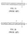
- FIG. 1A to FIG. 1E which showing the manufacture process to produce the via on an integrated circuit substrate in prior art, as shown, the process is including the steps as follows:
- solder mask is the most common used material in filling process fro the PTH 14 , it is easy to form the gap space in the conducting plug 15 and to produce the popcorn, and further cause the difficulties of filling, the limitation of the diameter of the via, bad quality of electrical connection and bad reliability.
- the integrated circuit substrate that being made thru the conventional process is with the weakness such as bad reliability and bad intensity in the conducting plug, it always fails to meet the requirement from customer, also, the market competition is weak and the production cost is high. Therefore, the improvement of the process for producing via on the integrated circuit substrate is the major concern that every substrate manufacturer focused.
- the primary aspect of the present invention is to provide a pattern formation process for an integrated circuit substrate, which is not employing the conventional method of filling resin material directly in filling process but adapting the metal spray method, the metal vapor deposition method or any combination thereof to form the pattern including circuits and pads and stuff the vias and the PTHs.
- the second aspect of the present invention is to provide a pattern formation process for an integrated circuit substrate, which employs the metal spray method, the metal vapor deposition method or any combination thereof to form an entire metal layer on the position of the via, and further to flat the metal layer to fill up the via.
- the third aspect of the present invention is to provide a pattern formation process for an integrated circuit substrate, which uses the metal material for filling directly to make the PTH, therefore, the extra capture pad is not necessary, nor is the expensive production facility, meanwhile, the density of the layout of the circuit will be increased and the quality of the substrate is much better.
- the present invention is to provide a pattern formation process for an integrated circuit substrate, which comprises the following steps:
- the aforesaid steps can be repeated a few times to build up more dielectric layers, and further, one of the metal spray method, the metal vapor deposition method or any combination thereof can be adapted to form the circuit layer; which is so called the build-up process.
- FIG. 1A to FIG. 1E show the pattern formation process for an integrated circuit substrate in prior art.
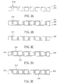
- FIG. 2A to FIG. 2M show the first embodiment of the pattern formation process for an integrated circuit substrate of the present invention.
- FIG. 3A to FIG. 3L shows the second embodiment of the pattern formation process for an integrated circuit substrate of the present invention.
- FIG. 2A to FIG. 2M are showing the first embodiment of the pattern formation process for an integrated circuit substrate of the present invention.
- the steps of forming the pattern and filling the via with conductive material are as follows:
- a substrate 110 which can be a ceramic substrate, a plastic substrate or a soft material substrate.
- the ceramic substrate uses the ceramic material as isolation while the plastic substrate uses the plastic material as isolation.
- the plastic substrate is the common one adapted in the industry, generally, the material for the plastic substrate is epoxy resin FR-4, BMI, BT-based resin, teflon, LCP, or polyimide.
- a protection sheet 111 will be placed on the surface of the substrate 110 , and on the predetermined position of the substrate 110 , a few through hole structure 13 a penetrating through the substrate 110 will be made by the mechanical drilling or the laser process.
- the metal material that being adapted in aforesaid method can be Cu, Al, Zn, Ag, Au, Ni or any other metal, and the metal spray method can be arc melting spray or high velocity particle consolidation;
- the metal can be Cu, Al or Zn, Ag, Au, Ni on both surface of the circuit substrate 110 ;
- the via will be defined by photolithography and curing process
- the metal layer 117 will be placed by the metal spray method or the metal vapor deposition method (ex. metal vapor evaporation method, the metal jet vapor deposition, etc.); wherein the metal can be Cu, Al, Zn, Ag, Au, Ni or other metal, to fill up the vias that being defined on the corresponding position of the metal through holes 113 as shown in FIG. 2H.
- (j).placing the isolation dielectric layer 118 over the via layer 117 , and the dielectric layer 115 and the material of the layer 118 can be a PID one or a laserable one and it should be the same material as used in layer 115 to form a new dielectric layer 119 .
- the opening for the circuit can be defined by the Photolithography and the curing process; if the layer 118 is a laserable one, the opening for the circuit on the dielectric layer 19 can be defined by the laser, but a release film should be placed first for protection, and the release film will be removed when the metal filling process completed.
- a metal layer 120 will be formed through release film protection on the layer 118 by metal spray method or metal vapor deposition method; wherein the metal can be Cu, Al, Zn, Ag, Au, Ni or other metal, to accomplish the filling up for circuit (FIG. 2M).
- the aforesaid steps can be repeated a few times to build up more dielectric layers, and further one of the metal spread method, metal vapor deposition method (ex. metal vapor evaporation method, the metal jet vapor deposition, etc.), or any combination thereof can be adapted to form the circuit layer; which is so called the build-up process.
- metal vapor deposition method ex. metal vapor evaporation method, the metal jet vapor deposition, etc.
- FIG. 3A to FIG. 3K are showing the second embodiment of the pattern formation process for an integrated circuit substrate of the present invention.
- the steps of manufacturing the via and filling the via with conductive material are as follows:
- a substrate 210 which can be a ceramic substrate, a plastic substrate or a soft material substrate.
- the ceramic substrate uses the ceramic material as isolation while the plastic substrate uses the plastic material as isolation.
- a protection sheet 211 will be placed on the surface (top one) of the substrate 210 , and on the predetermined position of the substrate 210 , a few through hole structure 213 a penetrating through the substrate 210 will be made by the mechanical drilling or the laser process.
- the metal material that being adapted in aforesaid method can be Cu, Al, Zn, Ag, Au, Ni or any other metal, and the metal spray method can be arc melting spray or high velocity particle consolidation;
- the layer 214 is a laserable one, a release film is over the dielectric layer 214 , and the position of the metal vias and the circuit layout on the dielectric layer 214 can be defined by the laser, then, the metal layer 215 will be formed by one of the metal spray method, metal vapor deposition method (ex. metal vapor evaporation method, the metal jet vapor deposition, etc.), or any combination thereof to proceed the filling, and the release film will be removed.
- metal vapor deposition method ex. metal vapor evaporation method, the metal jet vapor deposition, etc.
- the metal layer 215 will be formed by one of the metal spray method, the metal vapor deposition method (ex. metal vapor evaporation method, the metal jet vapor deposition, etc.), or any combination thereof on the layer 214 on the top and bottom surface of the substrate 210 to form the circuit layer 220 , wherein the metal can be Cu, Al, Zn, Ag, Au, Ni or other metal.
- the metal layer 218 will be formed by one of the metal spray method, the metal vapor deposition method (ex. metal vapor evaporation method, the metal jet vapor deposition, etc.), or any combination thereof to proceed the filling, and then the release film will be removed.
- the metal layer 218 will be formed by metal spray method or metal vapor deposition method on the dielectric layer 217 and the metal layer 215 ; wherein the metal can be Cu, Al, Zn, Ag, Au, Ni or other metal, to fill up the vias that being defined on the corresponding position of the metal through holes 213 on the dielectric layer 217 .
- the present embodiment can also apply to the so called build-up process.
- a few dielectric layers 217 are being stacked on the substrate 210 to form a multiple-layer substrate, and then one of the metal spray method, the metal vapor deposition method (ex. metal vapor evaporation method, the metal jet vapor deposition, etc.), or any combination thereof will be applied on the dielectric layers 217 to form a few circuit layers 220 , blind vias, embedded vias and through holes that penetrating the substrate.
- the aforesaid steps can be repeated a few times to build up more dielectric layers, and further one of the metal spray method, the metal vapor deposition method (ex. metal vapor evaporation method, the metal jet vapor deposition, etc.), or any combination thereof can be adapted to form the multiple circuit layer, which is so called build-up process.
- the metal spray method the metal vapor deposition method (ex. metal vapor evaporation method, the metal jet vapor deposition, etc.), or any combination thereof can be adapted to form the multiple circuit layer, which is so called build-up process.
- the present invention adapts one of the metal spray method, the metal vapor deposition method (ex. metal vapor evaporation method, the metal jet vapor deposition, etc.), or any combination thereof, with a release film and a protection sheet, to stuff the via on a substrate.
- the present invention adapts one of the metal spray method, the metal vapor deposition method (ex. metal vapor evaporation method, the metal jet vapor deposition, etc.), or any combination thereof, with a release film and a protection sheet, to stuff the via on a substrate.
- a via with vary small diameter, such as a diameter below 100 ⁇ m, even to 10 ⁇ m can be made and the quality of the structure of the via is excellent.
- the present invention adapts one of the metal spray method, metal vapor deposition method (ex. metal vapor evaporation method, the metal jet vapor deposition, etc.), or any combination thereof to form the entire metal layer, and further adapts proper flatting process to flat and stuff the metal through holes and vias.
- the manufacturing process is not only much easier and simpler than prior art but also keeps the excellent conductivity and yield rate.
- the present invention omits the complex process like photo resist process and adapts the PID or the laserable dielectric directly to define the position of through holes or vias; which make the filling process easier to complete.
- the description above is completely illustrating the pattern formation process for an integrated circuit substrate of the present invention.
- the present invention uses metal material to process the filling up to form through holes and vias; which will not use extra capture pad and expensive facility but highly increase the density of the circuit layout and the quality of substrate. More over, with the present invention, the manufacturing process is much easier and can be wildly used in many fields for various size of substrate, totally overcome the disadvantages in prior art.
Abstract
A pattern formation process for an integrated circuit substrate, which is not employing the conventional method of filling resin material directly in via filling process but adapting the metal spray method, the metal vapor deposition method or any combination thereof to form the pattern including circuits and pads and stuff the vias and the through holes.
Description
- (a) Field of the invention
- The present invention relates to a pattern formation process for an integrated circuit substrate. Especially, the present invention relates to a pattern formation process that uses the metal spray method, the metal vapor deposition method or any combination thereof applying on the integrated circuit substrate to stuff the vias and PTHs ((Plated Through Holes) and to form the pattern including circuits and pads.
- (b) Description of the Prior Art
- As the electronic product getting smaller and lighter, the circuit board and the substrate manufacturer now are facing the strict requirement for multiple layers integrated circuit substrate. The circuit layout placed on the substrate is using the vias and the PTHs to connect and conduct each other. Basically, the PTH is fully penetrating through a substrate, while a via is not when several substrates added together. In general, the diameter of the via or the PTH is less than 100 μm and its line width is less than 50 μm. However, for the purpose of the density and the precision, the technology for manufacturing the micro via or the PTH with high density and high precision on the single or multiple layers integrated circuit substrate has been developed rapidly. And as the circuit board being wildly used, with higher depth/width ratio, manufacturing PTH with good electrical characteristic on a substrate with high precision is the major concern for many manufacturers.
- Please refer to FIG. 1A to FIG. 1E, which showing the manufacture process to produce the via on an integrated circuit substrate in prior art, as shown, the process is including the steps as follows:
- (a) providing a basic material as the main body of integrated
circuit substrate 10, and on the top and the bottom side of the integratedcircuit substrate 10, placing the top andbottom metal layers - (b) allocating the position of the PTHs on the predetermined position on the surface of the integrated
circuit substrate 10, punching by the mechanical drilling to form a plurality of throughholes 13 on the integratedcircuit substrate 10; - (c) plating a complete plane with
copper 14 in the inner side of the throughholes 13 to form the electrical conducting PTHs (Plated Trough Hole) 13 a; - (d) proceeding Photolithograph, etching process on the circuit structure that being defined on the top and the
bottom metal layer circuit substrate 10 to define the top and thebottom circuit layer - (e) proceeding the filling process on the
PTH 13 a by filling up thePTH 13 a with a resin material such as the solder mask to form the complete structure of conductingplug 14, and the last step is to place the protection layer on the surface of the top and thebottom circuit layer circuit substrate 10 for protection purpose. - The description above is the general manufacturing process for a single layer integrated circuit substrate. Basically, defining the PTHs in the aforesaid process for the single layer integrated circuit substrate and stacking the single layer integrated circuit substrates together will form the complex multiple layers integrated circuit substrate.
- The process described above has been developed for many years in prior art, however, the disadvantages still exist; such as bad reliability, bad yield and so on. The major causes are as follows,
- 1. The solder mask is the most common used material in filling process fro the
PTH 14, it is easy to form the gap space in the conductingplug 15 and to produce the popcorn, and further cause the difficulties of filling, the limitation of the diameter of the via, bad quality of electrical connection and bad reliability. - 2. Making high quality via is a extremely complex process, the time for making such product is much longer, the manufacturing facility needed is expensive and the manufacturing cost is also high.
- As the descriptions, the integrated circuit substrate that being made thru the conventional process is with the weakness such as bad reliability and bad intensity in the conducting plug, it always fails to meet the requirement from customer, also, the market competition is weak and the production cost is high. Therefore, the improvement of the process for producing via on the integrated circuit substrate is the major concern that every substrate manufacturer focused.
- The primary aspect of the present invention is to provide a pattern formation process for an integrated circuit substrate, which is not employing the conventional method of filling resin material directly in filling process but adapting the metal spray method, the metal vapor deposition method or any combination thereof to form the pattern including circuits and pads and stuff the vias and the PTHs.
- The second aspect of the present invention is to provide a pattern formation process for an integrated circuit substrate, which employs the metal spray method, the metal vapor deposition method or any combination thereof to form an entire metal layer on the position of the via, and further to flat the metal layer to fill up the via.
- The third aspect of the present invention is to provide a pattern formation process for an integrated circuit substrate, which uses the metal material for filling directly to make the PTH, therefore, the extra capture pad is not necessary, nor is the expensive production facility, meanwhile, the density of the layout of the circuit will be increased and the quality of the substrate is much better.
- In order to achieve the objects described above, the present invention is to provide a pattern formation process for an integrated circuit substrate, which comprises the following steps:
- (a).placing a protection sheet or a release sheet on the surface of a substrate, on the predetermined position of the circuit substrate, to form a few through hole structures penetrating through the substrate;
- (b).placing a protection sheet or a release sheet on the other surface of the substrate that has not been placed with a protection sheet and applying one of the metal spread method, metal vapor deposition method or any combination thereof to proceed the filling process to form the solid through hole;
- (c).releasing the protection sheet or the release sheet that have been placed on both surface (top and bottom) of the substrate and to proceed polishing, grinding or etching to make the surfaces plane.
- (d).applying one of the metal spray method, the metal vapor deposition method or any combination thereof to form a metal layer on the both surface of the substrate;
- (e).applying Photolithograph on the both metal layers to define circuit layer;
- (t).placing a dielectric layer; such as photo-imagible dielectric (PID) or laserable dielectric, on the circuit layer;
- (g).defining the corresponding position of the vias on the dielectric layer;
- (h).applying one of the metal spray method, the metal vapor deposition method or any combination thereof to form a metal layer on the surface of the dielectric layer and stuff the vias that being placed on the dielectric layer;
- (i).applying the grinding, the CMP or the SUEP (Surface Uniform Etching Process) on the most outer surface of the substrate surface planarization.
- The aforesaid steps can be repeated a few times to build up more dielectric layers, and further, one of the metal spray method, the metal vapor deposition method or any combination thereof can be adapted to form the circuit layer; which is so called the build-up process.
- FIG. 1A to FIG. 1E show the pattern formation process for an integrated circuit substrate in prior art.
- FIG. 2A to FIG. 2M show the first embodiment of the pattern formation process for an integrated circuit substrate of the present invention.
- FIG. 3A to FIG. 3L shows the second embodiment of the pattern formation process for an integrated circuit substrate of the present invention.
- The following embodiments will describe the pattern formation process for an integrated circuit substrate of the present invention about the detailed evolvement, the effect and the other technical characteristics.
- Please refer to FIG. 2A to FIG. 2M, which are showing the first embodiment of the pattern formation process for an integrated circuit substrate of the present invention. The steps of forming the pattern and filling the via with conductive material are as follows:
- (a) selecting a
substrate 110 which can be a ceramic substrate, a plastic substrate or a soft material substrate. The ceramic substrate uses the ceramic material as isolation while the plastic substrate uses the plastic material as isolation. And the plastic substrate is the common one adapted in the industry, generally, the material for the plastic substrate is epoxy resin FR-4, BMI, BT-based resin, teflon, LCP, or polyimide. Then, aprotection sheet 111 will be placed on the surface of thesubstrate 110, and on the predetermined position of thesubstrate 110, a few throughhole structure 13 a penetrating through thesubstrate 110 will be made by the mechanical drilling or the laser process. - (b).placing a
protection release sheet 112 on the other surface (the bottom one) of thecircuit substrate 110 that has not been placed with aprotection sheet 111 and applying one of the metal spray method, the metal vapor deposition method (ex. the metal vapor evaporation, the metal jet vapor deposition, etc.) or any combination thereof to proceed the filling process on thethrough hole structure 113 a to form the throughholes 113. The metal material that being adapted in aforesaid method can be Cu, Al, Zn, Ag, Au, Ni or any other metal, and the metal spray method can be arc melting spray or high velocity particle consolidation; - (c).releasing the
protection sheet 111 or therelease sheet 112 that have been placed on both surface (top and bottom) of thecircuit substrate 110 and proceeding the grinding or the etching or the CMP to make the surfaces plane; - (d).applying one of the metal spray method, the metal vapor deposition method (ex. the metal vapor evaporation, the metal jet vapor deposition, etc.), or any combination thereof to plate a
metal layer 114; the metal can be Cu, Al or Zn, Ag, Au, Ni on both surface of thecircuit substrate 110; - (e).applying Photolithograph on the both
metal layers 114 to define thecircuit layer 114 a on the surface of thesubstrate 110; - (f).applying an
insulation dielectric layer 115; such as the photo-imagible dielectric (PID) or the laserable dielectric, on thecircuit layer 114 a; and the number of the dielectric layer can be multiple; it is so called the build-up process; - (g).if the
dielectric layer 115 is a laserable one; as shown is FIG. 2G, arelease film 116 will be placed for protection purpose, and the vias will be defined on the corresponding position of the metal throughholes 113 on thedielectric layer 115, and one of the metal spray method, metal vapor deposition method (ex. metal vapor evaporation method, the metal jet vapor deposition, etc.), or any combination thereof will be applied to fill up the via structure; and then releasing therelease film 116 to form a structure shown in FIG. 2I. - (h). if the
dielectric layer 115 is a PID one, the via will be defined by photolithography and curing process, themetal layer 117 will be placed by the metal spray method or the metal vapor deposition method (ex. metal vapor evaporation method, the metal jet vapor deposition, etc.); wherein the metal can be Cu, Al, Zn, Ag, Au, Ni or other metal, to fill up the vias that being defined on the corresponding position of the metal throughholes 113 as shown in FIG. 2H. - (i).applying the grinding, the CMP or the SUEP on the most
outer metal layer 117 of thecircuit substrate 110 for the surface planarization as shown in FIG. 21 - (j).placing the
isolation dielectric layer 118 over the vialayer 117, and thedielectric layer 115 and the material of thelayer 118 can be a PID one or a laserable one and it should be the same material as used inlayer 115 to form anew dielectric layer 119. - (k).if the
dielectric layer 118 is a PID one, the opening for the circuit can be defined by the Photolithography and the curing process; if thelayer 118 is a laserable one, the opening for the circuit on the dielectric layer 19 can be defined by the laser, but a release film should be placed first for protection, and the release film will be removed when the metal filling process completed. - (l).if the
dielectric layer 118 is a laserable one, ametal layer 120 will be formed through release film protection on thelayer 118 by metal spray method or metal vapor deposition method; wherein the metal can be Cu, Al, Zn, Ag, Au, Ni or other metal, to accomplish the filling up for circuit (FIG. 2M). - (m).if the
dielectric layer 118 is a PID one, the grinding, the CMP or the SUEP will be applied on the mostouter metal layer 120 and the dielectric 119 of thecircuit substrate 110 for planarization (FIG. 2L). - The aforesaid steps can be repeated a few times to build up more dielectric layers, and further one of the metal spread method, metal vapor deposition method (ex. metal vapor evaporation method, the metal jet vapor deposition, etc.), or any combination thereof can be adapted to form the circuit layer; which is so called the build-up process.
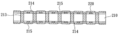
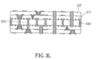
- Please refer to FIG. 3A to FIG. 3K, which are showing the second embodiment of the pattern formation process for an integrated circuit substrate of the present invention. The steps of manufacturing the via and filling the via with conductive material are as follows:
- (a) selecting a
substrate 210 which can be a ceramic substrate, a plastic substrate or a soft material substrate. The ceramic substrate uses the ceramic material as isolation while the plastic substrate uses the plastic material as isolation. Then, aprotection sheet 211 will be placed on the surface (top one) of thesubstrate 210, and on the predetermined position of thesubstrate 210, a few throughhole structure 213 a penetrating through thesubstrate 210 will be made by the mechanical drilling or the laser process. - (b).placing a
protection release sheet 212 on the other surface (the bottom one) of thecircuit substrate 210 that has not been placed with aprotection sheet 211, and applying one of the metal spray method, metal vapor deposition method (ex. metal vapor evaporation method, the metal jet vapor deposition, etc.) or any combination thereof to proceed the filling process on the throughhole structure 213 a to form the throughholes 213; the metal material that being adapted in aforesaid method can be Cu, Al, Zn, Ag, Au, Ni or any other metal, and the metal spray method can be arc melting spray or high velocity particle consolidation; - (c).releasing the
protection sheet 211 or therelease sheet 212 that have been placed on both surface (top and bottom) of thecircuit substrate 210, and proceeding the grinding or the etching to make the surfaces plane, - (d).placing one
isolation dielectric layer 214 on the both top and bottom surface of thesubstrate 210, and thedielectric layer 214 can be a PID one or a laserable one, - (e). if the
layer 214 is a laserable one, a release film is over thedielectric layer 214, and the position of the metal vias and the circuit layout on thedielectric layer 214 can be defined by the laser, then, themetal layer 215 will be formed by one of the metal spray method, metal vapor deposition method (ex. metal vapor evaporation method, the metal jet vapor deposition, etc.), or any combination thereof to proceed the filling, and the release film will be removed. - (f). if the
dielectric layer 214 is a PID one, a few metal vias and circuit layout will be defined on thedielectric layer 214 by the Photolithography or the curing process; then, themetal layer 215 will be formed by one of the metal spray method, the metal vapor deposition method (ex. metal vapor evaporation method, the metal jet vapor deposition, etc.), or any combination thereof on thelayer 214 on the top and bottom surface of thesubstrate 210 to form thecircuit layer 220, wherein the metal can be Cu, Al, Zn, Ag, Au, Ni or other metal. - (g). applying the grinding, the CMP or the SUEP on the
metal layer 215 of thecircuit substrate 210 to make the surfaces plane. - (h).applying an
isolation dielectric layer 216 on themetal layer 215 and thedielectric layer 214, and the material of thelayer 216 can be a PID one or a laserable one, and it should be the same material as used in thelayer 214 to form anew dielectric layer 217. - (i) if the
dielectric layer 217 is a laserable one, a release film is over thedielectric layer 217, and the position of the metal vias and the circuit layout on thedielectric layer 217 can be defined by the laser, then, themetal layer 218 will be formed by one of the metal spray method, the metal vapor deposition method (ex. metal vapor evaporation method, the metal jet vapor deposition, etc.), or any combination thereof to proceed the filling, and then the release film will be removed. - (j). if the
dielectric layer 217 is a PID one, a few metal vias and circuits will be defined on thedielectric layer 217 by the Photolithography or the curing process; then, themetal layer 218 will be formed by metal spray method or metal vapor deposition method on thedielectric layer 217 and themetal layer 215; wherein the metal can be Cu, Al, Zn, Ag, Au, Ni or other metal, to fill up the vias that being defined on the corresponding position of the metal throughholes 213 on thedielectric layer 217. - (k). applying the grinding, the CMP or the SUEP on the most
outer metal layer 218 of thecircuit substrate 210 for the surface planarization. - (l).the present embodiment can also apply to the so called build-up process. As shown in FIG. 3L, a few
dielectric layers 217 are being stacked on thesubstrate 210 to form a multiple-layer substrate, and then one of the metal spray method, the metal vapor deposition method (ex. metal vapor evaporation method, the metal jet vapor deposition, etc.), or any combination thereof will be applied on thedielectric layers 217 to form a few circuit layers 220, blind vias, embedded vias and through holes that penetrating the substrate. - The aforesaid steps can be repeated a few times to build up more dielectric layers, and further one of the metal spray method, the metal vapor deposition method (ex. metal vapor evaporation method, the metal jet vapor deposition, etc.), or any combination thereof can be adapted to form the multiple circuit layer, which is so called build-up process.
- The major difference in the present invention that differs from prior art is that the present invention adapts one of the metal spray method, the metal vapor deposition method (ex. metal vapor evaporation method, the metal jet vapor deposition, etc.), or any combination thereof, with a release film and a protection sheet, to stuff the via on a substrate. With the present invention, a via with vary small diameter, such as a diameter below 100 μm, even to 10 μm, can be made and the quality of the structure of the via is excellent.
- Further, the present invention adapts one of the metal spray method, metal vapor deposition method (ex. metal vapor evaporation method, the metal jet vapor deposition, etc.), or any combination thereof to form the entire metal layer, and further adapts proper flatting process to flat and stuff the metal through holes and vias. The manufacturing process is not only much easier and simpler than prior art but also keeps the excellent conductivity and yield rate.
- More over, the present invention omits the complex process like photo resist process and adapts the PID or the laserable dielectric directly to define the position of through holes or vias; which make the filling process easier to complete.
- The description above is completely illustrating the pattern formation process for an integrated circuit substrate of the present invention. As illustrated, the present invention uses metal material to process the filling up to form through holes and vias; which will not use extra capture pad and expensive facility but highly increase the density of the circuit layout and the quality of substrate. More over, with the present invention, the manufacturing process is much easier and can be wildly used in many fields for various size of substrate, totally overcome the disadvantages in prior art.
- While the present invention has been shown and described with reference to a preferred embodiment thereof, and in terms of the illustrative drawings, it should be not considered as limited thereby. Various possible modification, omission, and alterations could be conceived of by one skilled in the art to the form and the content of any particular embodiment, without departing from the scope and the spirit of the present invention.
Claims (17)
1. A conductive through hole formation process on an integrated circuit substrate, which comprising at lease the following steps:
(a) providing a substrate, and placing a release film on the substrate;
(b) forming at lease one through hole penetrating through the substrate and the release film;
(c) filling up the through hole by applying one of the methods of the metal spray, the metal vapor deposition, and the combination of both to form the conductive through hole in the substrate; and
(d) removing the release film.
2. A conductive through hole formation process on an integrated circuit substrate of claim 1 , wherein the step (b) is using one of the methods of the mechanical drilling and the laser drilling process.
3. A conductive through hole formation process on an integrated circuit substrate of claim 1 , wherein the metal spray method is including one of the methods of the arc melting spray and the high velocity particle consolidation.
4. A conductive through hole formation process on an integrated circuit substrate of claim 1 , wherein the metal vapor deposition is including one of the methods of the metal vapor evaporation and the metal jet vapor deposition.
5. A conductive through hole formation process on an integrated circuit substrate of claim 1 , wherein further comprising a step (e) following the step (d) to proceed a planarization process on the substrate.
6. A pattern formation process for an integrated circuit substrate, which comprising at least the following steps:
(a) providing a substrate, which already be finished the previous processes, with a dielectric layer on at least one surface;
(b) defining at least one via opening and a pattern simultaneously on the dielectric layer;
(c) forming a metal layer by applying one of the methods of the metal spray, the metal vapor deposition, and the combination of both on the substrate to fill up the via opening and form the conductive pattern; and
(d) proceed a planarization process on the metal layer.
7. A pattern formation process for an integrated circuit substrate of claim 6 , wherein the metal spray method is including one of the methods of the arc melting spray and the high velocity particle consolidation.
8. A pattern formation process for an integrated circuit substrate of claim 6 , wherein the metal vapor deposition is including one of the methods of the metal vapor evaporation and the metal jet vapor deposition.
9. A pattern formation process for an integrated circuit substrate of claim 6 , wherein the dielectric layer is a laserable dielectric layer, and the step (b) is using a laser drilling process.
10. A pattern formation process for an integrated circuit substrate of claim 9 , wherein a release film is applied to the surface of the dielectric layer before the laser drilling process, and the release film is removed after the laser drilling process.
11. A pattern formation process for an integrated circuit substrate of claim 6 , wherein the dielectric layer is a photo-imagible dielectric (PID) layer, and the step (b) is using a photolithography and curing process.
12. A pattern formation process for an integrated circuit substrate, which comprising at least the following steps:
(a) providing a substrate, which already be finished the previous processes, with a dielectric layer on at least one surface;
(b) defining at least one via opening on the dielectric layer;
(c) forming a metal layer by applying one of the methods of the metal spray, the metal vapor deposition, and the combination of both on the substrate to fill up the via opening; and
(d) proceed a planarization process on the metal layer.
13. A pattern formation process for an integrated circuit substrate of claim 11 , wherein the metal spray method is including one of the methods of the arc melting spray and the high velocity particle consolidation.
14. A pattern formation process for an integrated circuit substrate of claim 11 , wherein the metal vapor deposition is including one of the methods of the metal vapor evaporation and the metal jet vapor deposition.
15. A pattern formation process for an integrated circuit substrate of claim 11 , wherein the dielectric layer is a laserable dielectric layer, and the step (b) is using a laser drilling process.
16. A pattern formation process for an integrated circuit substrate of claim 15 , wherein a release film is applied to the surface of the dielectric layer before the laser drilling process, and the release film is removed after the laser drilling process.
17. A pattern formation process for an integrated circuit substrate of claim 11 , wherein the dielectric layer is a photo-imagible dielectric (PID) layer, and the step (b) is using a photolithography and curing process.
Applications Claiming Priority (2)
| Application Number | Priority Date | Filing Date | Title |
|---|---|---|---|
| TW91107134 | 2002-04-09 | ||
| TW091107134A TW558823B (en) | 2002-04-10 | 2002-04-10 | Through-hole process of integrated circuit substrate |
Publications (2)
| Publication Number | Publication Date |
|---|---|
| US20030190799A1 true US20030190799A1 (en) | 2003-10-09 |
| US6881662B2 US6881662B2 (en) | 2005-04-19 |
Family
ID=28673335
Family Applications (1)
| Application Number | Title | Priority Date | Filing Date |
|---|---|---|---|
| US10/211,700 Expired - Lifetime US6881662B2 (en) | 2002-04-10 | 2002-08-02 | Pattern formation process for an integrated circuit substrate |
Country Status (2)
| Country | Link |
|---|---|
| US (1) | US6881662B2 (en) |
| TW (1) | TW558823B (en) |
Cited By (7)
| Publication number | Priority date | Publication date | Assignee | Title |
|---|---|---|---|---|
| US20060071347A1 (en) * | 2004-10-04 | 2006-04-06 | Sharp Kabushiki Kaisha | Semiconductor device and fabrication method thereof |
| US20080220373A1 (en) * | 2007-03-07 | 2008-09-11 | Samsung Electro-Mechanics Co., Ltd. | Method for forming a photoresist-laminated substrate, method for plating an insulating substrate, method for surface treating of a metal layer of a circuit board, and method for manufacturing a multi layer ceramic condenser using metal nanoparticles aerosol |
| US7544304B2 (en) | 2006-07-11 | 2009-06-09 | Electro Scientific Industries, Inc. | Process and system for quality management and analysis of via drilling |
| US20100044092A1 (en) * | 2008-08-20 | 2010-02-25 | Electro Scientific Industries, Inc. | Method and apparatus for optically transparent via filling |
| US7886437B2 (en) | 2007-05-25 | 2011-02-15 | Electro Scientific Industries, Inc. | Process for forming an isolated electrically conductive contact through a metal package |
| US20110052828A1 (en) * | 2009-09-03 | 2011-03-03 | Randy Allen Normann | Method for high-temperature ceramic circuits |
| CN111276443A (en) * | 2020-02-10 | 2020-06-12 | 中国电子科技集团公司第十三研究所 | Preparation method of microwave thin film hybrid integrated circuit |
Families Citing this family (5)
| Publication number | Priority date | Publication date | Assignee | Title |
|---|---|---|---|---|
| JP2004039867A (en) * | 2002-07-03 | 2004-02-05 | Sony Corp | Multilayer wiring circuit module and its manufacturing method |
| DE102004050476B3 (en) * | 2004-10-16 | 2006-04-06 | Infineon Technologies Ag | Making wiring circuit panel, employs structured masking layers to define through-contact locations, with selective use of protective layers when depositing conductor structures |
| US7405146B2 (en) * | 2006-01-24 | 2008-07-29 | Kinsus Interconnect Technology Corp. | Electroplating method by transmitting electric current from a ball side |
| US20070257339A1 (en) * | 2006-05-08 | 2007-11-08 | Taiwan Semiconductor Manufacturing Co., Ltd. | Shield structures |
| CN103510033B (en) * | 2012-06-28 | 2017-07-28 | 富瑞精密组件(昆山)有限公司 | The preparation method of metal works |
Citations (9)
| Publication number | Priority date | Publication date | Assignee | Title |
|---|---|---|---|---|
| US5118385A (en) * | 1991-05-28 | 1992-06-02 | Microelectronics And Computer Technology Corporation | Multilayer electrical interconnect fabrication with few process steps |
| US5122227A (en) * | 1986-10-31 | 1992-06-16 | Texas Instruments Incorporated | Method of making a monolithic integrated magnetic circuit |
| US5382315A (en) * | 1991-02-11 | 1995-01-17 | Microelectronics And Computer Technology Corporation | Method of forming etch mask using particle beam deposition |
| US5877076A (en) * | 1997-10-14 | 1999-03-02 | Industrial Technology Research Institute | Opposed two-layered photoresist process for dual damascene patterning |
| US5891527A (en) * | 1995-09-15 | 1999-04-06 | M/Wave | Printed circuit board process using plasma spraying of conductive metal |
| US6163957A (en) * | 1998-11-13 | 2000-12-26 | Fujitsu Limited | Multilayer laminated substrates with high density interconnects and methods of making the same |
| US6521533B1 (en) * | 1999-09-14 | 2003-02-18 | Commissariat A L'energie Atomique | Method for producing a copper connection |
| US20030203705A1 (en) * | 2002-04-26 | 2003-10-30 | Yaojian Leng | Chemical-mechanical polishing slurry with improved defectivity |
| US6640434B1 (en) * | 2000-04-11 | 2003-11-04 | Lear Corporation | Method of forming an electrical circuit on a substrate |
-
2002
- 2002-04-10 TW TW091107134A patent/TW558823B/en not_active IP Right Cessation
- 2002-08-02 US US10/211,700 patent/US6881662B2/en not_active Expired - Lifetime
Patent Citations (9)
| Publication number | Priority date | Publication date | Assignee | Title |
|---|---|---|---|---|
| US5122227A (en) * | 1986-10-31 | 1992-06-16 | Texas Instruments Incorporated | Method of making a monolithic integrated magnetic circuit |
| US5382315A (en) * | 1991-02-11 | 1995-01-17 | Microelectronics And Computer Technology Corporation | Method of forming etch mask using particle beam deposition |
| US5118385A (en) * | 1991-05-28 | 1992-06-02 | Microelectronics And Computer Technology Corporation | Multilayer electrical interconnect fabrication with few process steps |
| US5891527A (en) * | 1995-09-15 | 1999-04-06 | M/Wave | Printed circuit board process using plasma spraying of conductive metal |
| US5877076A (en) * | 1997-10-14 | 1999-03-02 | Industrial Technology Research Institute | Opposed two-layered photoresist process for dual damascene patterning |
| US6163957A (en) * | 1998-11-13 | 2000-12-26 | Fujitsu Limited | Multilayer laminated substrates with high density interconnects and methods of making the same |
| US6521533B1 (en) * | 1999-09-14 | 2003-02-18 | Commissariat A L'energie Atomique | Method for producing a copper connection |
| US6640434B1 (en) * | 2000-04-11 | 2003-11-04 | Lear Corporation | Method of forming an electrical circuit on a substrate |
| US20030203705A1 (en) * | 2002-04-26 | 2003-10-30 | Yaojian Leng | Chemical-mechanical polishing slurry with improved defectivity |
Cited By (18)
| Publication number | Priority date | Publication date | Assignee | Title |
|---|---|---|---|---|
| US20060071347A1 (en) * | 2004-10-04 | 2006-04-06 | Sharp Kabushiki Kaisha | Semiconductor device and fabrication method thereof |
| US7365440B2 (en) | 2004-10-04 | 2008-04-29 | Sharp Kabushiki Kaisha | Semiconductor device and fabrication method thereof |
| US8501021B2 (en) | 2006-07-11 | 2013-08-06 | Electro Scientific Industries, Inc. | Process and system for quality management and analysis of via drilling |
| US7544304B2 (en) | 2006-07-11 | 2009-06-09 | Electro Scientific Industries, Inc. | Process and system for quality management and analysis of via drilling |
| US20090179017A1 (en) * | 2006-07-11 | 2009-07-16 | Electro Scientific Industries, Inc. | Process and system for quality management and analysis of via drilling |
| US8003173B2 (en) * | 2007-03-07 | 2011-08-23 | Samsung Electro-Mechanics Co., Ltd. | Method for forming a photoresist-laminated substrate, method for plating an insulating substrate, method for surface treating of a metal layer of a circuit board, and method for manufacturing a multi layer ceramic condenser using metal nanoparticles aerosol |
| US20080220373A1 (en) * | 2007-03-07 | 2008-09-11 | Samsung Electro-Mechanics Co., Ltd. | Method for forming a photoresist-laminated substrate, method for plating an insulating substrate, method for surface treating of a metal layer of a circuit board, and method for manufacturing a multi layer ceramic condenser using metal nanoparticles aerosol |
| US7886437B2 (en) | 2007-05-25 | 2011-02-15 | Electro Scientific Industries, Inc. | Process for forming an isolated electrically conductive contact through a metal package |
| US20110131807A1 (en) * | 2007-05-25 | 2011-06-09 | Electro Scientific Industries, Inc. | Process for Forming an Isolated Electrically Conductive Contact Through a Metal Package |
| US8117744B2 (en) | 2007-05-25 | 2012-02-21 | Electro Scientific Industries, Inc. | Process for forming an isolated electrically conductive contact through a metal package |
| US7943862B2 (en) | 2008-08-20 | 2011-05-17 | Electro Scientific Industries, Inc. | Method and apparatus for optically transparent via filling |
| US20110151046A1 (en) * | 2008-08-20 | 2011-06-23 | Electro Scientific Industries, Inc. | Method and apparatus for optically transparent via filling |
| US20110147067A1 (en) * | 2008-08-20 | 2011-06-23 | Electro Scientific Industries, Inc. | Method and apparatus for optically transparent via filling |
| US20100044092A1 (en) * | 2008-08-20 | 2010-02-25 | Electro Scientific Industries, Inc. | Method and apparatus for optically transparent via filling |
| US8729404B2 (en) | 2008-08-20 | 2014-05-20 | Electro Scientific Industries, Inc. | Method and apparatus for optically transparent via filling |
| US8735740B2 (en) | 2008-08-20 | 2014-05-27 | Electro Scientific Industries, Inc. | Method and apparatus for optically transparent via filling |
| US20110052828A1 (en) * | 2009-09-03 | 2011-03-03 | Randy Allen Normann | Method for high-temperature ceramic circuits |
| CN111276443A (en) * | 2020-02-10 | 2020-06-12 | 中国电子科技集团公司第十三研究所 | Preparation method of microwave thin film hybrid integrated circuit |
Also Published As
| Publication number | Publication date |
|---|---|
| TW558823B (en) | 2003-10-21 |
| US6881662B2 (en) | 2005-04-19 |
Similar Documents
| Publication | Publication Date | Title |
|---|---|---|
| US6977348B2 (en) | High density laminated substrate structure and manufacture method thereof | |
| JP4716819B2 (en) | Manufacturing method of interposer | |
| TW548816B (en) | Formation method of conductor pillar | |
| US20080251495A1 (en) | Methods of preparing printed circuit boards and packaging substrates of integrated circuit | |
| JP4990826B2 (en) | Multilayer printed circuit board manufacturing method | |
| US6881662B2 (en) | Pattern formation process for an integrated circuit substrate | |
| US20120210576A1 (en) | Printed circuit board and method of manufacturing the same | |
| JP6590179B2 (en) | Method for terminating the sides of a multilayer composite electronic structure | |
| JP2007324559A (en) | Multilayer circuit board with fine pitch and fabricating method thereof | |
| TWI513379B (en) | Embedded passive component substrate and method for fabricating the same | |
| US20090242238A1 (en) | Buried pattern substrate | |
| US7728234B2 (en) | Coreless thin substrate with embedded circuits in dielectric layers and method for manufacturing the same | |
| US20030196987A1 (en) | Ultra fine patterning process for multi-layer substrate | |
| JP2006041029A (en) | Wiring substrate, manufacturing method thereof, and electronic device | |
| US20030082896A1 (en) | Hole metal-filling method | |
| US6913814B2 (en) | Lamination process and structure of high layout density substrate | |
| US20030215566A1 (en) | Fine patterning and fine solid via process for multi-layer substrate | |
| TW202226919A (en) | A method for manufactunring a multilayer circuit structure having embedded trace layers | |
| KR100689018B1 (en) | Printed circuit board with embedded coaxial cable and manufacturing method thereof | |
| TWI691243B (en) | Manufacturing method for printed circuit board | |
| US7807034B2 (en) | Manufacturing method of non-etched circuit board | |
| KR100729939B1 (en) | Method for manufacturing multi-layered pcb | |
| KR100450590B1 (en) | Method of forming a conducting layer on a dielectric layer for build-up pcb | |
| KR100652132B1 (en) | Printed circuit board and Method of manufacturing the same | |
| JPH05198901A (en) | Printed circuit board and manufacture thereof |
Legal Events
| Date | Code | Title | Description |
|---|---|---|---|
| AS | Assignment |
Owner name: VIA TECHNOLOGIES, INC., TAIWAN Free format text: ASSIGNMENT OF ASSIGNORS INTEREST;ASSIGNORS:KUNG, MORISS;HO, KWUN-YAO;REEL/FRAME:013172/0800 Effective date: 20020716 |
|
| STCF | Information on status: patent grant |
Free format text: PATENTED CASE |
|
| FPAY | Fee payment |
Year of fee payment: 4 |
|
| FPAY | Fee payment |
Year of fee payment: 8 |
|
| FPAY | Fee payment |
Year of fee payment: 12 |