US20030196589A1 - Laser annealing mask and method for smoothing an annealed surface - Google Patents
Laser annealing mask and method for smoothing an annealed surface Download PDFInfo
- Publication number
- US20030196589A1 US20030196589A1 US10/124,826 US12482602A US2003196589A1 US 20030196589 A1 US20030196589 A1 US 20030196589A1 US 12482602 A US12482602 A US 12482602A US 2003196589 A1 US2003196589 A1 US 2003196589A1
- Authority
- US
- United States
- Prior art keywords
- mask
- energy density
- laser beam
- microns
- substrate region
- Prior art date
- Legal status (The legal status is an assumption and is not a legal conclusion. Google has not performed a legal analysis and makes no representation as to the accuracy of the status listed.)
- Granted
Links
Images


Classifications
-
- C—CHEMISTRY; METALLURGY
- C30—CRYSTAL GROWTH
- C30B—SINGLE-CRYSTAL GROWTH; UNIDIRECTIONAL SOLIDIFICATION OF EUTECTIC MATERIAL OR UNIDIRECTIONAL DEMIXING OF EUTECTOID MATERIAL; REFINING BY ZONE-MELTING OF MATERIAL; PRODUCTION OF A HOMOGENEOUS POLYCRYSTALLINE MATERIAL WITH DEFINED STRUCTURE; SINGLE CRYSTALS OR HOMOGENEOUS POLYCRYSTALLINE MATERIAL WITH DEFINED STRUCTURE; AFTER-TREATMENT OF SINGLE CRYSTALS OR A HOMOGENEOUS POLYCRYSTALLINE MATERIAL WITH DEFINED STRUCTURE; APPARATUS THEREFOR
- C30B29/00—Single crystals or homogeneous polycrystalline material with defined structure characterised by the material or by their shape
- C30B29/02—Elements
- C30B29/06—Silicon
-
- C—CHEMISTRY; METALLURGY
- C30—CRYSTAL GROWTH
- C30B—SINGLE-CRYSTAL GROWTH; UNIDIRECTIONAL SOLIDIFICATION OF EUTECTIC MATERIAL OR UNIDIRECTIONAL DEMIXING OF EUTECTOID MATERIAL; REFINING BY ZONE-MELTING OF MATERIAL; PRODUCTION OF A HOMOGENEOUS POLYCRYSTALLINE MATERIAL WITH DEFINED STRUCTURE; SINGLE CRYSTALS OR HOMOGENEOUS POLYCRYSTALLINE MATERIAL WITH DEFINED STRUCTURE; AFTER-TREATMENT OF SINGLE CRYSTALS OR A HOMOGENEOUS POLYCRYSTALLINE MATERIAL WITH DEFINED STRUCTURE; APPARATUS THEREFOR
- C30B13/00—Single-crystal growth by zone-melting; Refining by zone-melting
Landscapes
- Chemical & Material Sciences (AREA)
- Engineering & Computer Science (AREA)
- Crystallography & Structural Chemistry (AREA)
- Materials Engineering (AREA)
- Metallurgy (AREA)
- Organic Chemistry (AREA)
- Recrystallisation Techniques (AREA)
- Laser Beam Processing (AREA)
Abstract
Description
- 1. Field of the Invention
- This invention generally relates to integrated circuit (IC) and liquid crystal display (LCD) fabrication and, more particularly, to a system and method for smoothing the surface of a crystallized substrate during a laser annealing process.
- 2. Description of the Related Art
- When forming thin film transistors (TFTs) for use in LCD or other microelectronic circuits, the location of transistors channel regions, the orientation of regular structured polycrystalline silicon (poly-Si) or single-grain-crystalline silicon, and the surface roughness are important issues. This poly-Si material can be used as the active layer of poly-Si TFTs in the fabrication of active-matrix (AM) backplanes. Such backplanes can be used in the fabrication of AM LCDs and can be also combined with other display technologies, such as organic light-emitting diodes (OLEDs).
- Poly-Si material is typically formed by the crystallization of initially deposited amorphous Si (a-Si) films. This process can be accomplished via solid-phase-crystallization (SPC), for example, by annealing the a-Si films in a furnace at appropriate temperature and for sufficiently long time. Alternatively, laser annealing can also be used to achieve the phase transformation.
- Conventionally, crystallization techniques are applied to a substrate in such a manner as to yield uniform poly-Si film quality throughout the substrate area. In other words, there is no spatial quality differentiation over the area of the substrate. The most important reason for this end result is the inability of conventional methods to achieve such quality differentiation. For example, when a-Si film is annealed in a furnace or by rapid-thermal-annealing, all of the film is exposed to the same temperature, resulting in the same quality of poly-Si material. In the case of conventional laser annealing, some differentiation is possible, but the price, in terms of loss of throughput, is very high for the modest performance gains realized.
- Recently, a new laser annealing technique has been developed that allows for significant flexibility in the process techniques, permitting controlled variation in resulting film microstructure. This technique relies on lateral growth of Si grains using very narrow laser beams, that are generated by passing a laser beam through a beam-shaping mask, and projecting the image of the mask to the film that is being annealed. The method is called Laser-Induced Lateral Growth (LILaC).
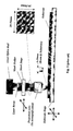
- FIG. 1 is a diagram illustrating the LILaC process (prior art). The initially amorphous silicon film is irradiated by a very narrow laser beamlet, with typical widths of a few microns (i.e. 3-5 μm). Such small beamlets are formed by passing the original laser beam through a mask that has open spaces or apertures (see FIG. 2), and projecting the beamlets onto the surface of the annealed Si-film.
- FIG. 2 is a conventional laser annealing mask (prior art). Returning to FIG. 1, the sequence of
images 1 through 4 illustrates the growth of long silicon grains. A step-and-repeat approach is used. The shaped laser “beamlet” (indicated by the 2 parallel, heavy black lines) irradiates the film and then steps by a distance smaller than half of the width of the slit. As a result of this deliberate advancement of each beamlet, grains are allowed to grow laterally from the crystal seeds of the poly-Si material formed in the previous step. This is equivalent to laterally “pulling” the crystals, as in zone-melting-crystallization (ZMR) method or other similar processes. As a result, the crystal tends to attain very high quality along the “pulling” direction, in the direction of the advancing beamlets. This process occurs simultaneously at each slit on the mask, allowing for rapid crystallization of the area covered by the projection of the mask on the substrate. Once this area is crystallized, the substrate moves to a new (unannealed) location and the process is repeated. - FIG. 3 is a pictorial representation of a system to accomplish the optical projection and the step-and repeat process (prior art). The LILaC process has the potential for creating intentional spatial variations in the quality of the poly-Si material. Such intentional variations can be beneficial for applications where multiple components are integrated on a display, where each component has different specifications and material performance requirements.
- Some poly-Si materials formed through the LILaC process have a highly periodical microstructure, where crystal bands of specific width are separated by high-angle grain boundaries. Within the crystal bands, low-angle boundaries are observed with a frequency of occurrence dependent upon certain specifics of the crystallization process, such as film thickness, laser fluence (energy density), pulse duration, and the like. TFTs fabricated on such poly-Si films demonstrate very good characteristics, as long as the direction of conduction is parallel to the direction of the in-crystal low-angle boundaries.
- TFTs with greater electron mobility can be fabricated if the substrate crystallization characteristics can be made more isotropic. In other words, the TFT performance depends upon the angle between the main crystalline growth direction, the direction parallel to the laser scanning axis, and the TFT channel. This is due to the formation of sub-boundaries within the crystal domains. The surface roughness at the “hard” grain boundaries, at the edges of the crystal bands/domains, can be significant. This surface roughness prohibits the reduction of the gate insulator thickness, which is one critical step for scaling down the device geometry for future applications. Further, not all these processes can be location controlled. Therefore, by chance only, depending upon the relative size of the crystal domain and the TFT channel length, certain TFTs will not include grain-boundaries in their active area (channel), whereas other TFTs will include one or more boundaries in their active areas. This kind of non-uniformity is highly detrimental for critical-application TFTs where uniformity of characteristics is more essential than absolute performance.
- It would be advantageous if the LILaC process could be modified to include a process of smoothing the substrate surface after laser annealing.
- It would be advantageous if the LILaC process could form TFT channel regions less dependent upon random process occurrences.
- The present invention method is used for smoothing the surface roughness of a silicon substrate during the crystallization process, using a surface “smoothing” mask feature. Making the substrate surface smooth enables improved TFT performance, with a simultaneous improvement in TFT reliability. The present invention process doesn't add time-consuming additional steps to the LILaC process.
- Accordingly, a method is provided for smoothing an annealed surface using a sub-resolution mask pattern. The method comprises: supplying a laser beam having a first wavelength; supplying a mask with a first mask section having apertures with a first dimension and a second mask section with apertures having a second dimension, less than the first dimension; applying a laser beam having a first energy density to a substrate region; melting a substrate region in response to the first energy density; crystallizing the substrate region; applying a diffracted laser beam to the substrate region; and, in response to the diffracted laser beam, smoothing the substrate region surface.
- In some aspects of the method, applying a diffracted laser beam to the substrate area includes applying a diffracted laser beam having a second energy density, less than the first energy density, to the substrate region. The second energy density is in the range of 40% to 70% of the first energy density, and preferably in the range of 50% to 60% of the first energy density.
- In some aspects, supplying a laser beam having a first wavelength includes the first wavelength being less than, or equal to the first dimension, and greater than the second dimension. Then, approximately 100% of the supplied laser beam is transmitted through the first mask region, while applying a diffracted laser beam having a second energy density, less than the first energy density, to the substrate region includes transmitting less than 100% of the supplied laser beam through the second mask region.
- Additional details of the above-described method and a laser annealing mask with sub-resolution aperture patterns are described below.
- FIG. 1 is a diagram illustrating the LILaC process (prior art).
- FIG. 2 is a conventional laser annealing mask (prior art).
- FIG. 3 is a pictorial representation of a system to accomplish the optical projection and the step-and repeat process (prior art).
- FIG. 4 is a plan view of the present invention laser annealing mask with sub-resolution aperture patterns.
- FIG. 5 depicts a variation of the sub-resolution mask of FIG. 4.
- FIGS. 6 a and 6 b depict mask diffraction sections.
- FIG. 7 is a flowchart illustrating the present invention method for smoothing an annealed surface using a sub-resolution mask pattern.
- FIG. 4 is a plan view of the present invention laser annealing mask with sub-resolution aperture patterns. The
mask 400 comprises at least onesection 402 with aperture patterns for transmitting approximately 100% of incident light, and at least onesection 404 with aperture patterns for diffracting incident light. - FIG. 5 depicts a variation of the sub-resolution mask of FIG. 4. As shown, mask 500 comprises a plurality of adjacent 100
% transmission sections 502 a, 502 b, and 502 c with aperture patterns for transmitting approximately 100% of incident light. Also shown, the mask 500 includes a plurality of adjacent sections 504 a through 504 f with aperture patterns for diffracting incident light. The number of adjacent 100% transmission sections typically varies between 2 and 5 (three are shown), although the present invention is not limited to any particular number. Likewise, the number of adjacent diffracting sections typically varies between 2 and 5. Such a mask would be useful in smoothing a laser annealed surface, regardless of the direction of mask with respect to the underlying substrate. - More specifically, a
first set 506 of a plurality of adjacent sections with aperture patterns for diffracting incident light is shown with a second set 508 of a plurality of adjacent sections with aperture patterns for transmitting approximately 100% of incident light, adjacent thefirst set 506. A third set 510 of a plurality of adjacent sections with aperture patterns for diffracting incident light is adjacent the second set 508. As mentioned above, the first andthird sets 506 and 510 typically include between 2 and 6 adjacent sections. Three adjacent sections are shown in each set. - FIGS. 6 a and 6 b depict mask diffraction sections. In some aspects, the mask includes aperture patterns for diffracting incident light formed as a plurality of line pattern apertures, as shown in FIG. 6a. The line pattern apertures includes a spacing between lines (slits) 600 in the range between 0.25 microns and 1.5 microns, and
line widths 602 in the range of 0.25 microns and 1.5 microns. - Alternately, as shown in FIG. 6 b, the aperture patterns for diffracting incident light includes a plurality of square spaced apertures with
square sides 604 in the range between 0.25 microns and 1.5 microns. Likewise, the sections between the aperture squares has a spacing 606 in the range between 0.25 microns and 1.5 microns. Other variations not shown would form the aperture patterns as rectangles or circles. Note, mask sections that transmit approximately 100% of incident light are well known. Any of these conventional types of mask sections can be used with the present invention sub-resolution mask. - The wavelength of light defines the ideal minimum mask aperture dimension that can completely pass a particular monochromatic beam of light. However, this is limit is only theoretical, as the resolution is actually limited by diffraction effects. In other words, as light passes through a mask that has patterns of certain dimensions, diffraction will occur. The diffraction generates a multitude of beamlets that propagate at various angles around a direction normal to the mask, determined by the Bragg's formula. If the projection lens (under the mask) could collect all of these beams then, in theory, it would be able to perfectly resolve the features of the mask. This “collection efficiency” is actually expressed by the numerical aperture (NA) of the lens—the higher NA is, the wider the collection angle is, hence, the higher the resolution of the optical system.
- As the feature size on the mask becomes smaller, that is, gets closer and closer to the wavelength of the light source, a higher collection efficiency is needed to resolve the pattern. Hence, a higher NA is required. Therefore, if the NA lens remains constant as the mask features become smaller, the light becomes diffracted. The result is a “blurred” pattern. The beam does not resolve the pattern because it is diffraction limited.
- Each mask section with aperture patterns for transmitting approximately 100% of incident light can be said to transmit a first energy density, or first fluence. Each mask section with aperture patterns for diffracting incident light can be said to transmit a second energy density, or second fluence, less than the first energy density. In some aspects, mask sections with aperture patterns for diffracting incident light transmits a second energy density that is 40% to 70% of the first energy density. Preferable, the second energy density is 50% to 60% of the first energy density.
- Functional Description
- The present invention method is simple and involves addition of “smoothing” regions at the edges of a standard LILaC mask. The smoothing regions are areas that are designed to intentionally diffract the beam and, consequently, reduce the laser fluence that reaches the surface of the substrate. With this configuration, the film is initially completely melted, to induce lateral growth, and then is only partially melted to promote surface reflow and smoothing of the ridges that develop at the points of congruence of grain boundaries.
- The design of the smoothing region of the mask can be accomplished by simulation of the optical properties of this region using appropriate software (i.e. SPLAT). The mask form of the smoothing regions is designed to irradiate the area on the substrate with the uniform fluence. The region of surface roughness is irradiated with less fluence than the fluence of the LILaC crystallization. But, the mask diffraction sections are not limited to the examples described above. Other patterns besides slits and squares can cause diffraction. Further, a filter can be used to reduce irradiation fluence. It should also be understood that the dimensions of the diffraction section apertures are dependent upon conditions such as the wavelength of the laser, the specification of optics, and the NA, to name a few examples.
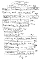
- FIG. 7 is a flowchart illustrating the present invention method for smoothing an annealed surface using a sub-resolution mask pattern. Although this method is depicted as a sequence of numbered steps for clarity, no order should be inferred from the numbering unless explicitly stated. It should be understood that some of these steps may be skipped, performed in parallel, or performed without the requirement of maintaining a strict order of sequence. The methods start at
Step 700. Step 702 supplies a laser beam having a first wavelength. Step 704 supplies a mask with a first mask section having apertures with a first dimension and a second mask section with apertures having a second dimension, less than the first dimension. Step 706 applies a laser beam having a first energy density to a substrate region. Step 708 melts a substrate region in response to the first energy density. Step 710 crystallizes the substrate region. Step 712 applies a diffracted laser beam to the substrate region.Step 714, in response to the diffracted laser beam, smoothes the substrate region surface. In some aspects Step 714 includes melting the substrate region surface to a thickness in the range of 200 Å to 300 Å. Alternately, Step 701 supplies a substrate film having a first thickness. Then, smoothing the substrate surface inStep 714 includes melting approximately 50% of the substrate film first thickness. - In some aspects of the method, applying a diffracted laser beam to the substrate area in
Step 712 includes applying a diffracted laser beam having a second energy density, less than the first energy density, to the substrate region. Typically, the second energy density is in the range of 40% to 70% of the first energy density. Preferably, the second energy density is in the range of 50% to 60% of the first energy density. - In other aspects, supplying a laser beam having a first wavelength in
Step 702 includes the first wavelength being less than, or equal to the first dimension, and greater than the second dimension. Applying a laser beam having a first energy density to a substrate region inStep 706 includes transmitting approximately 100% of the supplied laser beam through the first mask region. Then, applying a diffracted laser beam having a second energy density, less than the first energy density, to the substrate region inStep 712 includes transmitting less than 100% of the supplied laser beam through the second mask region. - In some aspects, applying a laser beam having a first energy density to a substrate region in
Step 706 includes substeps. Step 706 a applies the first energy density to a first area in the substrate region. Step 706 b step-and-repeats the application of the first energy density to a second area in the substrate region adjacent the first area. Likewise, applying a diffracted laser beam having a second energy density to the substrate region inStep 712 includes substeps. Step 712 a applies the second energy density to the first area. Step 712 b step-and-repeats the application of the second energy density to the second area. - In other aspects, supplying a mask with a second mask section with apertures having a second dimension in
Step 704 includes supplying a second mask section with a line pattern of apertures. Typically, the second mask section with a line pattern of apertures includes the spacing between lines being in the range between 0.25 microns and 1.5 microns, and the line widths being in the range of 0.25 microns and 1.5 microns. - Alternately, supplying a mask with a second mask section with apertures having a second dimension in
Step 704 includes supplying a second mask section with a square spaced pattern of apertures. Typically, the second mask section with the square spaced pattern of apertures includes the square sides being in the range between 0.25 microns and 1.5 microns, and sections between the aperture squares in the range between 0.25 microns and 1.5 microns. - A mask with sub-resolution aperture features and a method for using such a mask to smooth substrate surfaces as part of a laser annealing process have been described. A few examples have been given as to how such a mask could fabricated, but the present invention is not limited to just these examples. Likewise, an exemplary annealing process has been presented, but other variations of such a process are also practical. Other variation and embodiments of the invention will occur to those skilled in the art.
Claims (29)
Priority Applications (4)
| Application Number | Priority Date | Filing Date | Title |
|---|---|---|---|
| US10/124,826 US7192479B2 (en) | 2002-04-17 | 2002-04-17 | Laser annealing mask and method for smoothing an annealed surface |
| JP2003049796A JP2003309080A (en) | 2002-04-17 | 2003-02-26 | Method for smoothing annealed surface of substrate and mask for laser annealing |
| US10/913,678 US7029961B2 (en) | 2002-04-17 | 2004-08-05 | Method for optimized laser annealing smoothing |
| US11/653,057 US7804647B2 (en) | 2002-04-17 | 2007-01-13 | Sub-resolutional laser annealing mask |
Applications Claiming Priority (1)
| Application Number | Priority Date | Filing Date | Title |
|---|---|---|---|
| US10/124,826 US7192479B2 (en) | 2002-04-17 | 2002-04-17 | Laser annealing mask and method for smoothing an annealed surface |
Related Child Applications (2)
| Application Number | Title | Priority Date | Filing Date |
|---|---|---|---|
| US10/232,089 Continuation-In-Part US6777276B2 (en) | 2002-04-17 | 2002-08-29 | System and method for optimized laser annealing smoothing mask |
| US11/653,057 Division US7804647B2 (en) | 2002-04-17 | 2007-01-13 | Sub-resolutional laser annealing mask |
Publications (2)
| Publication Number | Publication Date |
|---|---|
| US20030196589A1 true US20030196589A1 (en) | 2003-10-23 |
| US7192479B2 US7192479B2 (en) | 2007-03-20 |
Family
ID=29214655
Family Applications (2)
| Application Number | Title | Priority Date | Filing Date |
|---|---|---|---|
| US10/124,826 Expired - Lifetime US7192479B2 (en) | 2002-04-17 | 2002-04-17 | Laser annealing mask and method for smoothing an annealed surface |
| US11/653,057 Expired - Fee Related US7804647B2 (en) | 2002-04-17 | 2007-01-13 | Sub-resolutional laser annealing mask |
Family Applications After (1)
| Application Number | Title | Priority Date | Filing Date |
|---|---|---|---|
| US11/653,057 Expired - Fee Related US7804647B2 (en) | 2002-04-17 | 2007-01-13 | Sub-resolutional laser annealing mask |
Country Status (2)
| Country | Link |
|---|---|
| US (2) | US7192479B2 (en) |
| JP (1) | JP2003309080A (en) |
Cited By (33)
| Publication number | Priority date | Publication date | Assignee | Title |
|---|---|---|---|---|
| US20040253840A1 (en) * | 2003-06-12 | 2004-12-16 | Lg.Philips Lcd Co., Ltd. | Method of crystallizing silicon |
| US20050139788A1 (en) * | 2003-12-29 | 2005-06-30 | You Jaesung | Laser mask and crystallization method using the same |
| US20050151196A1 (en) * | 2003-01-08 | 2005-07-14 | Hyun-Jae Kim | Polysilicon thin film transistor array panel and manufacturing method thereof |
| US20050221569A1 (en) * | 2004-03-31 | 2005-10-06 | Nec Corporation | Semiconductor thin film manufacturing method and device, beam-shaping mask, and thin film transistor |
| US20050233224A1 (en) * | 2004-04-20 | 2005-10-20 | Toppoly Optoelectronics Corp. | Method of improving polysilicon film crystallinity |
| US20070155102A1 (en) * | 2005-12-29 | 2007-07-05 | Infineon Technologies Ag | Method of fabricating an integrated circuit |
| US20080176414A1 (en) * | 2003-09-16 | 2008-07-24 | Columbia University | Systems and methods for inducing crystallization of thin films using multiple optical paths |
| US20080237593A1 (en) * | 2005-01-07 | 2008-10-02 | Junichiro Nakayama | Semiconductor Device, Method of Fabricating the Same, and Apparatus for Fabricating the Same |
| US20090242805A1 (en) * | 2005-08-16 | 2009-10-01 | Im James S | Systems and methods for uniform sequential lateral solidification of thin films using high frequency lasers |
| US7902052B2 (en) | 2003-02-19 | 2011-03-08 | The Trustees Of Columbia University In The City Of New York | System and process for processing a plurality of semiconductor thin films which are crystallized using sequential lateral solidification techniques |
| US7906414B2 (en) | 2002-08-19 | 2011-03-15 | The Trustees Of Columbia University In The City Of New York | Single-shot semiconductor processing system and method having various irradiation patterns |
| US8012861B2 (en) | 2007-11-21 | 2011-09-06 | The Trustees Of Columbia University In The City Of New York | Systems and methods for preparing epitaxially textured polycrystalline films |
| US8063338B2 (en) | 2003-09-16 | 2011-11-22 | The Trustees Of Columbia In The City Of New York | Enhancing the width of polycrystalline grains with mask |
| US20120012760A1 (en) * | 2010-07-16 | 2012-01-19 | Won-Kyu Lee | Laser irradiation apparatus |
| US8221544B2 (en) | 2005-04-06 | 2012-07-17 | The Trustees Of Columbia University In The City Of New York | Line scan sequential lateral solidification of thin films |
| US8278659B2 (en) | 1996-05-28 | 2012-10-02 | The Trustees Of Columbia University In The City Of New York | Uniform large-grained and grain boundary location manipulated polycrystalline thin film semiconductors formed using sequential lateral solidification and devices formed thereon |
| US8411713B2 (en) | 2002-08-19 | 2013-04-02 | The Trustees Of Columbia University In The City Of New York | Process and system for laser crystallization processing of film regions on a substrate to minimize edge areas, and structure of such film regions |
| US8415670B2 (en) | 2007-09-25 | 2013-04-09 | The Trustees Of Columbia University In The City Of New York | Methods of producing high uniformity in thin film transistor devices fabricated on laterally crystallized thin films |
| US8426296B2 (en) | 2007-11-21 | 2013-04-23 | The Trustees Of Columbia University In The City Of New York | Systems and methods for preparing epitaxially textured polycrystalline films |
| US8440581B2 (en) | 2009-11-24 | 2013-05-14 | The Trustees Of Columbia University In The City Of New York | Systems and methods for non-periodic pulse sequential lateral solidification |
| US8445365B2 (en) | 2003-09-19 | 2013-05-21 | The Trustees Of Columbia University In The City Of New York | Single scan irradiation for crystallization of thin films |
| US8476144B2 (en) | 2003-09-16 | 2013-07-02 | The Trustees Of Columbia University In The City Of New York | Method for providing a continuous motion sequential lateral solidification for reducing or eliminating artifacts in edge regions, and a mask for facilitating such artifact reduction/elimination |
| US8557040B2 (en) | 2007-11-21 | 2013-10-15 | The Trustees Of Columbia University In The City Of New York | Systems and methods for preparation of epitaxially textured thick films |
| US8569155B2 (en) | 2008-02-29 | 2013-10-29 | The Trustees Of Columbia University In The City Of New York | Flash lamp annealing crystallization for large area thin films |
| US8598588B2 (en) | 2005-12-05 | 2013-12-03 | The Trustees Of Columbia University In The City Of New York | Systems and methods for processing a film, and thin films |
| US8614471B2 (en) | 2007-09-21 | 2013-12-24 | The Trustees Of Columbia University In The City Of New York | Collections of laterally crystallized semiconductor islands for use in thin film transistors |
| US8663387B2 (en) | 2003-09-16 | 2014-03-04 | The Trustees Of Columbia University In The City Of New York | Method and system for facilitating bi-directional growth |
| US8715412B2 (en) | 2003-09-16 | 2014-05-06 | The Trustees Of Columbia University In The City Of New York | Laser-irradiated thin films having variable thickness |
| US8734584B2 (en) | 2004-11-18 | 2014-05-27 | The Trustees Of Columbia University In The City Of New York | Systems and methods for creating crystallographic-orientation controlled poly-silicon films |
| US8796159B2 (en) | 2003-09-16 | 2014-08-05 | The Trustees Of Columbia University In The City Of New York | Processes and systems for laser crystallization processing of film regions on a substrate utilizing a line-type beam, and structures of such film regions |
| US8802580B2 (en) | 2008-11-14 | 2014-08-12 | The Trustees Of Columbia University In The City Of New York | Systems and methods for the crystallization of thin films |
| US9087696B2 (en) | 2009-11-03 | 2015-07-21 | The Trustees Of Columbia University In The City Of New York | Systems and methods for non-periodic pulse partial melt film processing |
| US9646831B2 (en) | 2009-11-03 | 2017-05-09 | The Trustees Of Columbia University In The City Of New York | Advanced excimer laser annealing for thin films |
Families Citing this family (21)
| Publication number | Priority date | Publication date | Assignee | Title |
|---|---|---|---|---|
| KR100796758B1 (en) * | 2001-11-14 | 2008-01-22 | 삼성전자주식회사 | A mask for crystallizing polysilicon and a method for forming thin film transistor using the mask |
| WO2004017382A2 (en) * | 2002-08-19 | 2004-02-26 | The Trustees Of Columbia University In The City Of New York | Process and system for laser crystallization processing of film regions on a substrate to provide substantial uniformity within areas in such regions and edge areas thereof, and a structure of such film regions |
| US7364952B2 (en) * | 2003-09-16 | 2008-04-29 | The Trustees Of Columbia University In The City Of New York | Systems and methods for processing thin films |
| JP4413569B2 (en) * | 2003-09-25 | 2010-02-10 | 株式会社 日立ディスプレイズ | Display panel manufacturing method and display panel |
| KR100997971B1 (en) * | 2003-11-19 | 2010-12-02 | 삼성전자주식회사 | Mask for solidification, method for solidify and method for manufacturing a thin film transistor array panel including the method |
| KR20050068207A (en) | 2003-12-29 | 2005-07-05 | 엘지.필립스 엘시디 주식회사 | Laser mask having 2-block and method of crystallization using thereof |
| JP2005276944A (en) * | 2004-03-23 | 2005-10-06 | Sharp Corp | Semiconductor device, and device and method for manufacturing the same |
| US8653409B1 (en) | 2004-06-23 | 2014-02-18 | Board Of Governors For Higher Education, State Of Rhode Island And Providence Plantations | Selective surface smoothing using lasers |
| JP2006190897A (en) * | 2005-01-07 | 2006-07-20 | Sharp Corp | Semiconductor device, its manufacturing method and manufacturing equipment |
| JP2006210789A (en) * | 2005-01-31 | 2006-08-10 | Sharp Corp | Method for manufacturing semiconductor crystal thin film, its manufacturing apparatus, photomask and semiconductor device |
| JP2009505432A (en) * | 2005-08-16 | 2009-02-05 | ザ トラスティーズ オブ コロンビア ユニヴァーシティ イン ザ シティ オブ ニューヨーク | High-throughput crystallization of thin films |
| JP2007287866A (en) * | 2006-04-14 | 2007-11-01 | Sharp Corp | Method for manufacturing semiconductor crystal thin film and manufacturing apparatus thereof, photomask, and semiconductor element |
| JP2009135448A (en) * | 2007-11-01 | 2009-06-18 | Semiconductor Energy Lab Co Ltd | Method for manufacturing semiconductor substrate, and method for manufacturing semiconductor device |
| US8536054B2 (en) * | 2008-01-18 | 2013-09-17 | Miasole | Laser polishing of a solar cell substrate |
| US8546172B2 (en) | 2008-01-18 | 2013-10-01 | Miasole | Laser polishing of a back contact of a solar cell |
| US8586398B2 (en) * | 2008-01-18 | 2013-11-19 | Miasole | Sodium-incorporation in solar cell substrates and contacts |
| KR101413370B1 (en) * | 2008-02-29 | 2014-06-30 | 더 트러스티이스 오브 콜롬비아 유니버시티 인 더 시티 오브 뉴욕 | Flash light annealing for thin films |
| US8434937B2 (en) | 2008-05-30 | 2013-05-07 | Applied Materials, Inc. | Method and apparatus for detecting the substrate temperature in a laser anneal system |
| CN103862169B (en) | 2012-12-12 | 2016-08-10 | 中芯国际集成电路制造(上海)有限公司 | Laser annealing apparatus and method |
| CN103728827B (en) * | 2013-12-26 | 2016-07-06 | 深圳市华星光电技术有限公司 | Photomask, thin-film transistor element and the method making thin-film transistor element |
| JP7161758B2 (en) * | 2018-12-27 | 2022-10-27 | 株式会社ブイ・テクノロジー | Laser annealing equipment |
Citations (6)
| Publication number | Priority date | Publication date | Assignee | Title |
|---|---|---|---|---|
| US4970546A (en) * | 1988-04-07 | 1990-11-13 | Nikon Corporation | Exposure control device |
| US5365875A (en) * | 1991-03-25 | 1994-11-22 | Fuji Xerox Co., Ltd. | Semiconductor element manufacturing method |
| US5395481A (en) * | 1993-10-18 | 1995-03-07 | Regents Of The University Of California | Method for forming silicon on a glass substrate |
| US5825023A (en) * | 1997-03-26 | 1998-10-20 | The Hong Kong University Of Science & Technology | Auto focus laser encoder having three light beams and a reflective grating |
| US6322625B2 (en) * | 1996-05-28 | 2001-11-27 | The Trustees Of Columbia University In The City Of New York | Crystallization processing of semiconductor film regions on a substrate, and devices made therewith |
| US20040043606A1 (en) * | 2002-08-29 | 2004-03-04 | Crowder Mark Albert | System and method for optimized laser annealing smoothing mask |
Family Cites Families (3)
| Publication number | Priority date | Publication date | Assignee | Title |
|---|---|---|---|---|
| US5703675A (en) * | 1992-01-17 | 1997-12-30 | Nikon Corporation | Projection-exposing apparatus with deflecting grating member |
| JP3588212B2 (en) * | 1996-12-20 | 2004-11-10 | 株式会社ルネサステクノロジ | Exposure mask, method for manufacturing the same, and method for manufacturing semiconductor device |
| JP3302926B2 (en) * | 1998-07-02 | 2002-07-15 | 株式会社東芝 | Inspection method for exposure equipment |
-
2002
- 2002-04-17 US US10/124,826 patent/US7192479B2/en not_active Expired - Lifetime
-
2003
- 2003-02-26 JP JP2003049796A patent/JP2003309080A/en active Pending
-
2007
- 2007-01-13 US US11/653,057 patent/US7804647B2/en not_active Expired - Fee Related
Patent Citations (7)
| Publication number | Priority date | Publication date | Assignee | Title |
|---|---|---|---|---|
| US4970546A (en) * | 1988-04-07 | 1990-11-13 | Nikon Corporation | Exposure control device |
| US5365875A (en) * | 1991-03-25 | 1994-11-22 | Fuji Xerox Co., Ltd. | Semiconductor element manufacturing method |
| US5395481A (en) * | 1993-10-18 | 1995-03-07 | Regents Of The University Of California | Method for forming silicon on a glass substrate |
| US6322625B2 (en) * | 1996-05-28 | 2001-11-27 | The Trustees Of Columbia University In The City Of New York | Crystallization processing of semiconductor film regions on a substrate, and devices made therewith |
| US5825023A (en) * | 1997-03-26 | 1998-10-20 | The Hong Kong University Of Science & Technology | Auto focus laser encoder having three light beams and a reflective grating |
| US20040043606A1 (en) * | 2002-08-29 | 2004-03-04 | Crowder Mark Albert | System and method for optimized laser annealing smoothing mask |
| US6777276B2 (en) * | 2002-08-29 | 2004-08-17 | Sharp Laboratories Of America, Inc. | System and method for optimized laser annealing smoothing mask |
Cited By (57)
| Publication number | Priority date | Publication date | Assignee | Title |
|---|---|---|---|---|
| US8859436B2 (en) | 1996-05-28 | 2014-10-14 | The Trustees Of Columbia University In The City Of New York | Uniform large-grained and grain boundary location manipulated polycrystalline thin film semiconductors formed using sequential lateral solidification and devices formed thereon |
| US8278659B2 (en) | 1996-05-28 | 2012-10-02 | The Trustees Of Columbia University In The City Of New York | Uniform large-grained and grain boundary location manipulated polycrystalline thin film semiconductors formed using sequential lateral solidification and devices formed thereon |
| US8680427B2 (en) | 1996-05-28 | 2014-03-25 | The Trustees Of Columbia University In The City Of New York | Uniform large-grained and gain boundary location manipulated polycrystalline thin film semiconductors formed using sequential lateral solidification and devices formed thereon |
| US8883656B2 (en) | 2002-08-19 | 2014-11-11 | The Trustees Of Columbia University In The City Of New York | Single-shot semiconductor processing system and method having various irradiation patterns |
| US8479681B2 (en) | 2002-08-19 | 2013-07-09 | The Trustees Of Columbia University In The City Of New York | Single-shot semiconductor processing system and method having various irradiation patterns |
| US8411713B2 (en) | 2002-08-19 | 2013-04-02 | The Trustees Of Columbia University In The City Of New York | Process and system for laser crystallization processing of film regions on a substrate to minimize edge areas, and structure of such film regions |
| US7906414B2 (en) | 2002-08-19 | 2011-03-15 | The Trustees Of Columbia University In The City Of New York | Single-shot semiconductor processing system and method having various irradiation patterns |
| US20050151196A1 (en) * | 2003-01-08 | 2005-07-14 | Hyun-Jae Kim | Polysilicon thin film transistor array panel and manufacturing method thereof |
| US7294857B2 (en) * | 2003-01-08 | 2007-11-13 | Samsung Electronics Co., Ltd. | Polysilicon thin film transistor array panel and manufacturing method thereof |
| US7902052B2 (en) | 2003-02-19 | 2011-03-08 | The Trustees Of Columbia University In The City Of New York | System and process for processing a plurality of semiconductor thin films which are crystallized using sequential lateral solidification techniques |
| US20040253840A1 (en) * | 2003-06-12 | 2004-12-16 | Lg.Philips Lcd Co., Ltd. | Method of crystallizing silicon |
| DE102004028331B4 (en) * | 2003-06-12 | 2011-02-24 | Lg Display Co., Ltd. | Process for crystallizing silicon |
| US7977217B2 (en) * | 2003-06-12 | 2011-07-12 | Lg Display Co., Ltd. | Method of crystallizing silicon |
| US8034698B2 (en) | 2003-09-16 | 2011-10-11 | The Trustees Of Columbia University In The City Of New York | Systems and methods for inducing crystallization of thin films using multiple optical paths |
| US8063338B2 (en) | 2003-09-16 | 2011-11-22 | The Trustees Of Columbia In The City Of New York | Enhancing the width of polycrystalline grains with mask |
| US8476144B2 (en) | 2003-09-16 | 2013-07-02 | The Trustees Of Columbia University In The City Of New York | Method for providing a continuous motion sequential lateral solidification for reducing or eliminating artifacts in edge regions, and a mask for facilitating such artifact reduction/elimination |
| US8796159B2 (en) | 2003-09-16 | 2014-08-05 | The Trustees Of Columbia University In The City Of New York | Processes and systems for laser crystallization processing of film regions on a substrate utilizing a line-type beam, and structures of such film regions |
| US8715412B2 (en) | 2003-09-16 | 2014-05-06 | The Trustees Of Columbia University In The City Of New York | Laser-irradiated thin films having variable thickness |
| US9466402B2 (en) | 2003-09-16 | 2016-10-11 | The Trustees Of Columbia University In The City Of New York | Processes and systems for laser crystallization processing of film regions on a substrate utilizing a line-type beam, and structures of such film regions |
| US8663387B2 (en) | 2003-09-16 | 2014-03-04 | The Trustees Of Columbia University In The City Of New York | Method and system for facilitating bi-directional growth |
| US20080176414A1 (en) * | 2003-09-16 | 2008-07-24 | Columbia University | Systems and methods for inducing crystallization of thin films using multiple optical paths |
| US8445365B2 (en) | 2003-09-19 | 2013-05-21 | The Trustees Of Columbia University In The City Of New York | Single scan irradiation for crystallization of thin films |
| US20100173481A1 (en) * | 2003-12-29 | 2010-07-08 | You Jaesung | Laser mask and crystallization method using the same |
| GB2409765B (en) * | 2003-12-29 | 2006-08-23 | Lg Philips Lcd Co Ltd | Laser mask and crystallization method using the same |
| US7714331B2 (en) | 2003-12-29 | 2010-05-11 | Lg Display Co., Ltd. | Display device |
| US20050139788A1 (en) * | 2003-12-29 | 2005-06-30 | You Jaesung | Laser mask and crystallization method using the same |
| US7892955B2 (en) | 2003-12-29 | 2011-02-22 | Lg Display Co., Ltd. | Laser mask and crystallization method using the same |
| US8470696B2 (en) | 2003-12-29 | 2013-06-25 | Lg Display Co., Ltd. | Laser mask and crystallization method using the same |
| GB2409765A (en) * | 2003-12-29 | 2005-07-06 | Lg Philips Lcd Co Ltd | Mask for three-shot sequential lateral solidification |
| US20080106686A1 (en) * | 2003-12-29 | 2008-05-08 | You Jaesung | Laser mask and crystallization method using the same |
| US7316871B2 (en) | 2003-12-29 | 2008-01-08 | Lg.Philips Lcd Co., Ltd. | Laser mask and crystallization method using the same |
| US7611577B2 (en) * | 2004-03-31 | 2009-11-03 | Nec Corporation | Semiconductor thin film manufacturing method and device, beam-shaping mask, and thin film transistor |
| US20050221569A1 (en) * | 2004-03-31 | 2005-10-06 | Nec Corporation | Semiconductor thin film manufacturing method and device, beam-shaping mask, and thin film transistor |
| US20100019175A1 (en) * | 2004-03-31 | 2010-01-28 | Nec Corporation | Semiconductor manufacturing device and beam-shaping mask |
| US20050233224A1 (en) * | 2004-04-20 | 2005-10-20 | Toppoly Optoelectronics Corp. | Method of improving polysilicon film crystallinity |
| US8734584B2 (en) | 2004-11-18 | 2014-05-27 | The Trustees Of Columbia University In The City Of New York | Systems and methods for creating crystallographic-orientation controlled poly-silicon films |
| US20080237593A1 (en) * | 2005-01-07 | 2008-10-02 | Junichiro Nakayama | Semiconductor Device, Method of Fabricating the Same, and Apparatus for Fabricating the Same |
| US8617313B2 (en) | 2005-04-06 | 2013-12-31 | The Trustees Of Columbia University In The City Of New York | Line scan sequential lateral solidification of thin films |
| US8221544B2 (en) | 2005-04-06 | 2012-07-17 | The Trustees Of Columbia University In The City Of New York | Line scan sequential lateral solidification of thin films |
| US20090242805A1 (en) * | 2005-08-16 | 2009-10-01 | Im James S | Systems and methods for uniform sequential lateral solidification of thin films using high frequency lasers |
| US8598588B2 (en) | 2005-12-05 | 2013-12-03 | The Trustees Of Columbia University In The City Of New York | Systems and methods for processing a film, and thin films |
| US7622374B2 (en) | 2005-12-29 | 2009-11-24 | Infineon Technologies Ag | Method of fabricating an integrated circuit |
| US20070155102A1 (en) * | 2005-12-29 | 2007-07-05 | Infineon Technologies Ag | Method of fabricating an integrated circuit |
| US9012309B2 (en) | 2007-09-21 | 2015-04-21 | The Trustees Of Columbia University In The City Of New York | Collections of laterally crystallized semiconductor islands for use in thin film transistors |
| US8614471B2 (en) | 2007-09-21 | 2013-12-24 | The Trustees Of Columbia University In The City Of New York | Collections of laterally crystallized semiconductor islands for use in thin film transistors |
| US8415670B2 (en) | 2007-09-25 | 2013-04-09 | The Trustees Of Columbia University In The City Of New York | Methods of producing high uniformity in thin film transistor devices fabricated on laterally crystallized thin films |
| US8871022B2 (en) | 2007-11-21 | 2014-10-28 | The Trustees Of Columbia University In The City Of New York | Systems and methods for preparation of epitaxially textured thick films |
| US8012861B2 (en) | 2007-11-21 | 2011-09-06 | The Trustees Of Columbia University In The City Of New York | Systems and methods for preparing epitaxially textured polycrystalline films |
| US8426296B2 (en) | 2007-11-21 | 2013-04-23 | The Trustees Of Columbia University In The City Of New York | Systems and methods for preparing epitaxially textured polycrystalline films |
| US8557040B2 (en) | 2007-11-21 | 2013-10-15 | The Trustees Of Columbia University In The City Of New York | Systems and methods for preparation of epitaxially textured thick films |
| US8569155B2 (en) | 2008-02-29 | 2013-10-29 | The Trustees Of Columbia University In The City Of New York | Flash lamp annealing crystallization for large area thin films |
| US8802580B2 (en) | 2008-11-14 | 2014-08-12 | The Trustees Of Columbia University In The City Of New York | Systems and methods for the crystallization of thin films |
| US9646831B2 (en) | 2009-11-03 | 2017-05-09 | The Trustees Of Columbia University In The City Of New York | Advanced excimer laser annealing for thin films |
| US9087696B2 (en) | 2009-11-03 | 2015-07-21 | The Trustees Of Columbia University In The City Of New York | Systems and methods for non-periodic pulse partial melt film processing |
| US8440581B2 (en) | 2009-11-24 | 2013-05-14 | The Trustees Of Columbia University In The City Of New York | Systems and methods for non-periodic pulse sequential lateral solidification |
| US8889569B2 (en) | 2009-11-24 | 2014-11-18 | The Trustees Of Columbia University In The City Of New York | Systems and methods for non-periodic pulse sequential lateral soldification |
| US20120012760A1 (en) * | 2010-07-16 | 2012-01-19 | Won-Kyu Lee | Laser irradiation apparatus |
Also Published As
| Publication number | Publication date |
|---|---|
| JP2003309080A (en) | 2003-10-31 |
| US20070107655A1 (en) | 2007-05-17 |
| US7804647B2 (en) | 2010-09-28 |
| US7192479B2 (en) | 2007-03-20 |
Similar Documents
| Publication | Publication Date | Title |
|---|---|---|
| US7804647B2 (en) | Sub-resolutional laser annealing mask | |
| US7029961B2 (en) | Method for optimized laser annealing smoothing | |
| US6959029B2 (en) | Apparatus for performing anastomosis | |
| US6755909B2 (en) | Method of crystallizing amorphous silicon using a mask | |
| US6590228B2 (en) | LCD device with optimized channel characteristics | |
| US6921434B2 (en) | Regulated growth method for laser irradiating silicon films | |
| US7357963B2 (en) | Apparatus and method of crystallizing amorphous silicon | |
| US8118937B2 (en) | Semiconductor thin film, thin film transistor, method for manufacturing same, and manufacturing equipment of semiconductor thin film | |
| KR20060046344A (en) | Crystallizing method, thin-film transistor manufacturing method, thin-film transistor, and display device | |
| JP2004031809A (en) | Photomask and method of crystallizing semiconductor thin film | |
| US6727125B2 (en) | Multi-pattern shadow mask system and method for laser annealing | |
| US7384476B2 (en) | Method for crystallizing silicon | |
| US6709910B1 (en) | Method for reducing surface protrusions in the fabrication of lilac films | |
| US20020102821A1 (en) | Mask pattern design to improve quality uniformity in lateral laser crystallized poly-Si films | |
| JP2002280569A (en) | Method for forming thin film transistor on polycrystalline silicon film mainly oriented in <100> plane | |
| US6660576B2 (en) | Substrate and method for producing variable quality substrate material | |
| US8009345B2 (en) | Crystallization apparatus, crystallization method, device, and light modulation element | |
| US6656270B2 (en) | Excimer laser crystallization of amorphous silicon film | |
| WO2004066372A1 (en) | Crystallized semiconductor device, method for producing same and crystallization apparatus | |
| US6607971B1 (en) | Method for extending a laser annealing pulse | |
| JP2006054222A (en) | Optical modulation element, crystallization device, crystallization method, manufacturing device of thin-film semiconductor substrate, manufacturing method of thin-film semiconductor substrate, thin-film semiconductor device, manufacturing method of thin-film semiconductor device, and display device | |
| KR20000027517A (en) | Method for manufacturing polysilicon thin film transistors | |
| JP2009060128A (en) | Phase shift mask |
Legal Events
| Date | Code | Title | Description |
|---|---|---|---|
| AS | Assignment |
Owner name: SHARP LABORATORIES OF AMERICA, INC., WASHINGTON Free format text: ASSIGNMENT OF ASSIGNORS INTEREST;ASSIGNORS:MITANI, YASUHIRO;VOUTSAS, APOSTOLOS T.;CROWDER, MARK A.;REEL/FRAME:012827/0026 Effective date: 20020417 |
|
| STCF | Information on status: patent grant |
Free format text: PATENTED CASE |
|
| AS | Assignment |
Owner name: SHARP KABUSHIKI KAISHA, JAPAN Free format text: ASSIGNMENT OF ASSIGNORS INTEREST;ASSIGNOR:SHARP LABORATORIES OF AMERICA, INC.;REEL/FRAME:019246/0798 Effective date: 20070504 |
|
| FPAY | Fee payment |
Year of fee payment: 4 |
|
| FEPP | Fee payment procedure |
Free format text: PAYER NUMBER DE-ASSIGNED (ORIGINAL EVENT CODE: RMPN); ENTITY STATUS OF PATENT OWNER: LARGE ENTITY Free format text: PAYOR NUMBER ASSIGNED (ORIGINAL EVENT CODE: ASPN); ENTITY STATUS OF PATENT OWNER: LARGE ENTITY |
|
| FPAY | Fee payment |
Year of fee payment: 8 |
|
| MAFP | Maintenance fee payment |
Free format text: PAYMENT OF MAINTENANCE FEE, 12TH YEAR, LARGE ENTITY (ORIGINAL EVENT CODE: M1553) Year of fee payment: 12 |