US20030196748A1 - Process of fabricating a precision microcontact printing stamp - Google Patents
Process of fabricating a precision microcontact printing stamp Download PDFInfo
- Publication number
- US20030196748A1 US20030196748A1 US10/127,374 US12737402A US2003196748A1 US 20030196748 A1 US20030196748 A1 US 20030196748A1 US 12737402 A US12737402 A US 12737402A US 2003196748 A1 US2003196748 A1 US 2003196748A1
- Authority
- US
- United States
- Prior art keywords
- backplane
- accordance
- stamp
- flat
- adhesive
- Prior art date
- Legal status (The legal status is an assumption and is not a legal conclusion. Google has not performed a legal analysis and makes no representation as to the accuracy of the status listed.)
- Granted
Links
Images


Classifications
-
- B—PERFORMING OPERATIONS; TRANSPORTING
- B32—LAYERED PRODUCTS
- B32B—LAYERED PRODUCTS, i.e. PRODUCTS BUILT-UP OF STRATA OF FLAT OR NON-FLAT, e.g. CELLULAR OR HONEYCOMB, FORM
- B32B43/00—Operations specially adapted for layered products and not otherwise provided for, e.g. repairing; Apparatus therefor
- B32B43/006—Delaminating
-
- B—PERFORMING OPERATIONS; TRANSPORTING
- B29—WORKING OF PLASTICS; WORKING OF SUBSTANCES IN A PLASTIC STATE IN GENERAL
- B29C—SHAPING OR JOINING OF PLASTICS; SHAPING OF MATERIAL IN A PLASTIC STATE, NOT OTHERWISE PROVIDED FOR; AFTER-TREATMENT OF THE SHAPED PRODUCTS, e.g. REPAIRING
- B29C39/00—Shaping by casting, i.e. introducing the moulding material into a mould or between confining surfaces without significant moulding pressure; Apparatus therefor
- B29C39/02—Shaping by casting, i.e. introducing the moulding material into a mould or between confining surfaces without significant moulding pressure; Apparatus therefor for making articles of definite length, i.e. discrete articles
- B29C39/10—Shaping by casting, i.e. introducing the moulding material into a mould or between confining surfaces without significant moulding pressure; Apparatus therefor for making articles of definite length, i.e. discrete articles incorporating preformed parts or layers, e.g. casting around inserts or for coating articles
-
- B—PERFORMING OPERATIONS; TRANSPORTING
- B29—WORKING OF PLASTICS; WORKING OF SUBSTANCES IN A PLASTIC STATE IN GENERAL
- B29C—SHAPING OR JOINING OF PLASTICS; SHAPING OF MATERIAL IN A PLASTIC STATE, NOT OTHERWISE PROVIDED FOR; AFTER-TREATMENT OF THE SHAPED PRODUCTS, e.g. REPAIRING
- B29C39/00—Shaping by casting, i.e. introducing the moulding material into a mould or between confining surfaces without significant moulding pressure; Apparatus therefor
- B29C39/02—Shaping by casting, i.e. introducing the moulding material into a mould or between confining surfaces without significant moulding pressure; Apparatus therefor for making articles of definite length, i.e. discrete articles
- B29C39/12—Making multilayered or multicoloured articles
- B29C39/123—Making multilayered articles
- B29C39/126—Making multilayered articles by casting between two preformed layers, e.g. deformable layers
-
- B—PERFORMING OPERATIONS; TRANSPORTING
- B82—NANOTECHNOLOGY
- B82Y—SPECIFIC USES OR APPLICATIONS OF NANOSTRUCTURES; MEASUREMENT OR ANALYSIS OF NANOSTRUCTURES; MANUFACTURE OR TREATMENT OF NANOSTRUCTURES
- B82Y10/00—Nanotechnology for information processing, storage or transmission, e.g. quantum computing or single electron logic
-
- B—PERFORMING OPERATIONS; TRANSPORTING
- B82—NANOTECHNOLOGY
- B82Y—SPECIFIC USES OR APPLICATIONS OF NANOSTRUCTURES; MEASUREMENT OR ANALYSIS OF NANOSTRUCTURES; MANUFACTURE OR TREATMENT OF NANOSTRUCTURES
- B82Y40/00—Manufacture or treatment of nanostructures
-
- G—PHYSICS
- G03—PHOTOGRAPHY; CINEMATOGRAPHY; ANALOGOUS TECHNIQUES USING WAVES OTHER THAN OPTICAL WAVES; ELECTROGRAPHY; HOLOGRAPHY
- G03F—PHOTOMECHANICAL PRODUCTION OF TEXTURED OR PATTERNED SURFACES, e.g. FOR PRINTING, FOR PROCESSING OF SEMICONDUCTOR DEVICES; MATERIALS THEREFOR; ORIGINALS THEREFOR; APPARATUS SPECIALLY ADAPTED THEREFOR
- G03F7/00—Photomechanical, e.g. photolithographic, production of textured or patterned surfaces, e.g. printing surfaces; Materials therefor, e.g. comprising photoresists; Apparatus specially adapted therefor
- G03F7/0002—Lithographic processes using patterning methods other than those involving the exposure to radiation, e.g. by stamping
-
- H—ELECTRICITY
- H05—ELECTRIC TECHNIQUES NOT OTHERWISE PROVIDED FOR
- H05K—PRINTED CIRCUITS; CASINGS OR CONSTRUCTIONAL DETAILS OF ELECTRIC APPARATUS; MANUFACTURE OF ASSEMBLAGES OF ELECTRICAL COMPONENTS
- H05K3/00—Apparatus or processes for manufacturing printed circuits
- H05K3/10—Apparatus or processes for manufacturing printed circuits in which conductive material is applied to the insulating support in such a manner as to form the desired conductive pattern
- H05K3/12—Apparatus or processes for manufacturing printed circuits in which conductive material is applied to the insulating support in such a manner as to form the desired conductive pattern using thick film techniques, e.g. printing techniques to apply the conductive material or similar techniques for applying conductive paste or ink patterns
- H05K3/1275—Apparatus or processes for manufacturing printed circuits in which conductive material is applied to the insulating support in such a manner as to form the desired conductive pattern using thick film techniques, e.g. printing techniques to apply the conductive material or similar techniques for applying conductive paste or ink patterns by other printing techniques, e.g. letterpress printing, intaglio printing, lithographic printing, offset printing
-
- B—PERFORMING OPERATIONS; TRANSPORTING
- B29—WORKING OF PLASTICS; WORKING OF SUBSTANCES IN A PLASTIC STATE IN GENERAL
- B29L—INDEXING SCHEME ASSOCIATED WITH SUBCLASS B29C, RELATING TO PARTICULAR ARTICLES
- B29L2031/00—Other particular articles
- B29L2031/756—Microarticles, nanoarticles
-
- B—PERFORMING OPERATIONS; TRANSPORTING
- B29—WORKING OF PLASTICS; WORKING OF SUBSTANCES IN A PLASTIC STATE IN GENERAL
- B29L—INDEXING SCHEME ASSOCIATED WITH SUBCLASS B29C, RELATING TO PARTICULAR ARTICLES
- B29L2031/00—Other particular articles
- B29L2031/757—Moulds, cores, dies
-
- B—PERFORMING OPERATIONS; TRANSPORTING
- B32—LAYERED PRODUCTS
- B32B—LAYERED PRODUCTS, i.e. PRODUCTS BUILT-UP OF STRATA OF FLAT OR NON-FLAT, e.g. CELLULAR OR HONEYCOMB, FORM
- B32B2310/00—Treatment by energy or chemical effects
- B32B2310/08—Treatment by energy or chemical effects by wave energy or particle radiation
- B32B2310/0806—Treatment by energy or chemical effects by wave energy or particle radiation using electromagnetic radiation
- B32B2310/0831—Treatment by energy or chemical effects by wave energy or particle radiation using electromagnetic radiation using UV radiation
-
- B—PERFORMING OPERATIONS; TRANSPORTING
- B32—LAYERED PRODUCTS
- B32B—LAYERED PRODUCTS, i.e. PRODUCTS BUILT-UP OF STRATA OF FLAT OR NON-FLAT, e.g. CELLULAR OR HONEYCOMB, FORM
- B32B2310/00—Treatment by energy or chemical effects
- B32B2310/08—Treatment by energy or chemical effects by wave energy or particle radiation
- B32B2310/0806—Treatment by energy or chemical effects by wave energy or particle radiation using electromagnetic radiation
- B32B2310/0843—Treatment by energy or chemical effects by wave energy or particle radiation using electromagnetic radiation using laser
-
- B—PERFORMING OPERATIONS; TRANSPORTING
- B32—LAYERED PRODUCTS
- B32B—LAYERED PRODUCTS, i.e. PRODUCTS BUILT-UP OF STRATA OF FLAT OR NON-FLAT, e.g. CELLULAR OR HONEYCOMB, FORM
- B32B37/00—Methods or apparatus for laminating, e.g. by curing or by ultrasonic bonding
- B32B37/12—Methods or apparatus for laminating, e.g. by curing or by ultrasonic bonding characterised by using adhesives
-
- H—ELECTRICITY
- H05—ELECTRIC TECHNIQUES NOT OTHERWISE PROVIDED FOR
- H05K—PRINTED CIRCUITS; CASINGS OR CONSTRUCTIONAL DETAILS OF ELECTRIC APPARATUS; MANUFACTURE OF ASSEMBLAGES OF ELECTRICAL COMPONENTS
- H05K2201/00—Indexing scheme relating to printed circuits covered by H05K1/00
- H05K2201/01—Dielectrics
- H05K2201/0104—Properties and characteristics in general
- H05K2201/0133—Elastomeric or compliant polymer
-
- H—ELECTRICITY
- H05—ELECTRIC TECHNIQUES NOT OTHERWISE PROVIDED FOR
- H05K—PRINTED CIRCUITS; CASINGS OR CONSTRUCTIONAL DETAILS OF ELECTRIC APPARATUS; MANUFACTURE OF ASSEMBLAGES OF ELECTRICAL COMPONENTS
- H05K2203/00—Indexing scheme relating to apparatus or processes for manufacturing printed circuits covered by H05K3/00
- H05K2203/01—Tools for processing; Objects used during processing
- H05K2203/0104—Tools for processing; Objects used during processing for patterning or coating
- H05K2203/0108—Male die used for patterning, punching or transferring
-
- Y—GENERAL TAGGING OF NEW TECHNOLOGICAL DEVELOPMENTS; GENERAL TAGGING OF CROSS-SECTIONAL TECHNOLOGIES SPANNING OVER SEVERAL SECTIONS OF THE IPC; TECHNICAL SUBJECTS COVERED BY FORMER USPC CROSS-REFERENCE ART COLLECTIONS [XRACs] AND DIGESTS
- Y10—TECHNICAL SUBJECTS COVERED BY FORMER USPC
- Y10S—TECHNICAL SUBJECTS COVERED BY FORMER USPC CROSS-REFERENCE ART COLLECTIONS [XRACs] AND DIGESTS
- Y10S156/00—Adhesive bonding and miscellaneous chemical manufacture
- Y10S156/918—Delaminating processes adapted for specified product, e.g. delaminating medical specimen slide
- Y10S156/919—Delaminating in preparation for post processing recycling step
- Y10S156/922—Specified electronic component delaminating in preparation for recycling
-
- Y—GENERAL TAGGING OF NEW TECHNOLOGICAL DEVELOPMENTS; GENERAL TAGGING OF CROSS-SECTIONAL TECHNOLOGIES SPANNING OVER SEVERAL SECTIONS OF THE IPC; TECHNICAL SUBJECTS COVERED BY FORMER USPC CROSS-REFERENCE ART COLLECTIONS [XRACs] AND DIGESTS
- Y10—TECHNICAL SUBJECTS COVERED BY FORMER USPC
- Y10T—TECHNICAL SUBJECTS COVERED BY FORMER US CLASSIFICATION
- Y10T156/00—Adhesive bonding and miscellaneous chemical manufacture
- Y10T156/11—Methods of delaminating, per se; i.e., separating at bonding face
Definitions
- the present invention is directed to a formation of a microcontact printing stamp employed in the creation of microcircuitry where dimensional integrity and registration must be maintained at the micron level over very large distances that may be as long as half a meter. More particularly, the present invention is directed to a process of preparing a high precision microcontact printing stamp based on temporary rigid immobilization of the printing stamp backplane by glue lamination during curing.
- the very fine pitch rubber stamp utilized in microcontact printing is most often formed of an elastomeric material which is usually silicone rubber.
- silicone rubber denotes polydimethylsiloxane (PDMS).
- PDMS polydimethylsiloxane
- PDMS it should be appreciated, denotes the reactive monomer, a reactive oligomer or a mixture thereof as well as filler and polymerization catalysts.
- the positive relief pattern provided on the rubber stamp is thereupon inked onto a substrate.
- the substrate is blanket coated with a thin gold film and the gold coated substrate is inked with an alkane thiol material transferred thereto by the stamp.
- the alkane thiol material has the structural formula CH 3 —(CH 2 ) 18 —CHSH 2 . It should, of course, be appreciated that other alkane thiol materials, as well as other inks, can be substituted for this alkane thiol.
- a monolayer of the ink preferably an alkane thiol, having the desired microcircuit pattern
- Alkane thiols form an ordered monolayer on gold by a self assembly process.
- a self assembled monolayer (SAM) of the desired pattern is formed on the gold layer.
- SAM self assembled monolayer
- the SAM is tightly packed and well adhered to the gold. As such, the SAM acts as an etch resist upon contact of a gold etching solution onto the stamped gold film layer.
- the inked substrate is immersed in a gold etching solution and all but the SAM is etched away to underlying layers below the gold layer.
- the SAM which is protected, and thus not affected by the etchant, is then stripped away leaving gold in the desired pattern.
- the aforementioned description is set forth in the Kumar et al. technical article.
- the Hidber et al. technical article utilizes a different procedure wherein the aforementioned rubber stamp is inked with a palladium catalyst and a pattern is again stamped onto a substrate.
- the positive release microcircuit pattern of palladium catalyst is subsequently immersed in an electroless plating solution which induces the desired microcircuit pattern by electroless plating.
- microcontact printing could not meet this challenge. This was because microcontact printing stamps could not satisfy the registration requirement because of shrinkage and other distortions imposed during printing stamp preparation. That is, the elastomeric polymer would shrink in the mold during printing stamp preparation. As those skilled in the art are aware, when an elastomeric polymer, such as silicone rubber, cures in a mold it shrinks to a degree of between about 0.1% to about 4%.
- This shrinkage has a magnifying effect in that it is oftentimes manifested by undulations in the backplane of the stamp which is characterized by a reversal of the pattern of distortion once printed. That is, wave crests created in the backplane, caused by shrinkage during curing, impart distortions to the microcircuit pattern at the top of the stamp when the backplane bottom of the stamp is straightened under tension.
- This undulation problem may be exacerbated by the natural lack of planarity of the backplane sheet. Such a situation may occur for as simple a reason as the sheet was formed in a rolling process.
- a new process has now been developed which results in the formation of a high precision microcontact printing stamp providing a positive relief microcircuit pattern faithful to the dimensional requirements of the desired microcircuit.
- a process of fabricating a high precision microcontact printing stamp is provided.
- a mold is provided in which a photoresist master defining a desired microcircuit pattern in negative relief is disposed above a backplane temporarily adhered to a flat and rigid substrate.
- An elastomeric monomer or oligomer system is thereupon introduced into the mold and the elastomeric monomer is thereupon cured to form an elastomeric microcontact stamp whose top surface defines the desired microcircuit in positive relief.
- the bottom of the microcontact stamp is defined by a laminate of the backplane adhered to the flat and rigid substrate. The thus formed microcontact stamp is removed from the mold and the rigid and flat substrate is separated from the backplane.
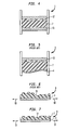
- FIG. 1 is a sectional elevation view of a mold prior to the introduction of an elastomeric monomer
- FIG. 2 is an exploded sectional view of one of components illustrated in FIG. 1;
- FIG. 3 is a sectional elevation view of the mold upon introduction of an elastomeric monomer
- FIG. 4 is a sectional elevational view of the mold upon curing of the elastomeric monomer to form an elastomeric resin
- FIG. 5 is a sectional elevation view of the mold upon curing of the elastomeric monomer to form an elastomeric resin in the absence of the inventive feature;
- FIG. 6 is a sectional elevation view of the microcontact stamp made in accordance with the prior art process illustrated in FIG. 5;
- FIG. 7 is a sectional elevational view of the microcontact stamp made in accordance with the present invention.
- a mold housing 1 is provided into which a photoresist master assembly 20 , which includes a photoresist master 3 , defining the desired microcircuit, disposed upon and affixed to a rigid substrate 2 , is predisposed above a flexible stamp backing assembly 15 which is more commonly referred to as a backplane assembly 15 .
- Backplane assemblies of the prior art were limited to a flexible member or, in an attempt to overcome the problems associated with the flexibility of the backplane, the backplane was disposed, in a non-adhering manner, upon a rigid plane, such as glass. It was originally believed that the pressure of the subsequent monomer or oligomer injection process flattened the backplane down against the rigid glass member and held it there. Actual experience has shown that injection pressure is inadequate.
- the backplane assembly 15 is a laminate of a flexible backplane 4 bonded to a flat and rigid planar member 5 . As shown in FIG. 2, the backplane laminate assembly 15 is formed by disposing backplane 4 upon a flat and rigid sheet 5 . An adhesive 11 is disposed between the backplane 4 and the sheet 5 .
- the flat and rigid member 5 is a glass sheet.
- FIG. 2 illustrates the flat plane 5 as being transparent, a characteristic of glass.
- the backplane 4 is a flexible material.
- this flexible material is a flexible metal.
- Such flexible metals as stainless steel, steel alloys containing nickel, e.g. Invar® alloys, nickel-titanium alloys, e.g. Nicol® alloys, and the like are thus particularly preferred for use as the backplane.
- a significant advance of the process of the present invention is addressed by providing a method of delaminating the backplane 4 from the rigid plane 5 .
- this result is obtained by utilizing a photodeblockable adhesive.
- photodeblockable adhesives strongly adhere to substrates but the adhesive is deblocked, and thus no longer adheres, if exposed to ultraviolet light.
- the advantage of the rigid and flat plane 5 being glass. Most glasses are transparent to ultraviolet light. Other flat and rigid planar materials that are ultraviolet light transparent, of course, may alternatively be utilized.
- the adhesive used in the formation of the laminate assembly 15 is an adhesive ablatively decomposable upon exposure to laser light.
- laser ablative adhesives employable in the present invention are polyacrylates, epoxies, polyimides, polyurethanes and the like. Again this methodology emphasizes the desirability of employing a laser transparent, flat and rigid plane 5 , a property that most glasses also possess to effectuate adhesive decomposition.
- the elastomeric monomer 6 which generically encompasses catalyst, promoters and the like, and which may also be oligomeric, is introduced into the mold so that it fills the space between the photoresist assembly 12 and the backplane assembly 15 .
- Preferred elastomeric monomers or oligomers include dimethylsiloxane, oligomers thereof, monomeric or oligomeric precursors of polyurethanes, epoxy rubbers, polyphosphazines, butadiene rubbers, vulcanized rubbers and the like.
- thermoset elastomeric product 7 whose top portion defines the microcircuit imparted by the photoresist master 3 .
- the thermoset polymerization reaction is typically conducted at a temperature in the range of between about 40° C. and about 80° C.
- the curing polymerization reaction occurs at a temperature in the range of between about 50° C. and about 70° C. Most preferably, the temperature of the elastomeric curing polymerization reaction is in the range of between about 55° C. and about 65° C. Indeed, these curing temperature ranges are particularly preferred when the preferred monomer, dimethylsiloxane, or an oligomer thereof is employed.
- the bottom of the thermoset polymerization product, the backplane assembly 15 is characterized by a flat undisturbed plane, due to firmness provided by the rigid and flat plane 5 layer of the assembly 15 .
- the microcircuit stamp 9 of the present invention when removed from mold housing 1 , subsequent to the delamination step of the rigid layer 5 of the backplane assembly 15 , has the appearance illustrated in FIG. 7. This desirable result occurs because the retention of the rigid plane 5 during the curing step insures proper alignment of the elastomeric microcircuit pattern 14 . This result also occurs because delamination, effected by ultraviolet or laser light exposure, is easily accomplished.
Abstract
Description
- 1. Field of the Invention
- The present invention is directed to a formation of a microcontact printing stamp employed in the creation of microcircuitry where dimensional integrity and registration must be maintained at the micron level over very large distances that may be as long as half a meter. More particularly, the present invention is directed to a process of preparing a high precision microcontact printing stamp based on temporary rigid immobilization of the printing stamp backplane by glue lamination during curing.
- 2. Background of the Prior Art
- The process of microcontact printing, to create a very fine pitch pattern, is of recent vintage in the art of fabricating microcircuitry. This process is described in Kumar et al., Appl. Phys. Lett., 63, (14), 2002-2004 (October 1993) and Hidber et al., Langmuir, 12, 1375-1380 (1996). This process, which represents an alternative to photolithography in the fabrication of electronic components, especially where extremely fine line dimensions are required, requires the creation of a very fine pitch rubber stamp.
- The very fine pitch rubber stamp utilized in microcontact printing is most often formed of an elastomeric material which is usually silicone rubber. Those skilled in the art are aware that the term “silicon rubber” denotes polydimethylsiloxane (PDMS). PDMS, it should be appreciated, denotes the reactive monomer, a reactive oligomer or a mixture thereof as well as filler and polymerization catalysts. In the current method of preparing rubber stamps used in high precision microcontact printing liquid PDMS is introduced into a mold wherein a negative relief microcircuit pattern is expressed. The polymer is thereupon cured to produce a solidified rubber stamp which is removed from the mold. The solidified rubber stamp has a microcircuit pattern expressed in positive relief. It is this pattern that is transferred to a substrate in subsequent steps in the microcontact printing process.
- The positive relief pattern provided on the rubber stamp is thereupon inked onto a substrate. Although there are several variations of microprinting methodology, commonly, the substrate is blanket coated with a thin gold film and the gold coated substrate is inked with an alkane thiol material transferred thereto by the stamp. Commonly, the alkane thiol material has the structural formula CH 3—(CH2)18—CHSH2. It should, of course, be appreciated that other alkane thiol materials, as well as other inks, can be substituted for this alkane thiol.
- Upon contact of the positive relief pattern of the stamp with the gold film, a monolayer of the ink, preferably an alkane thiol, having the desired microcircuit pattern, is transferred to the gold film layer. Alkane thiols form an ordered monolayer on gold by a self assembly process. Thus, a self assembled monolayer (SAM) of the desired pattern is formed on the gold layer. The SAM is tightly packed and well adhered to the gold. As such, the SAM acts as an etch resist upon contact of a gold etching solution onto the stamped gold film layer.
- In the next step, the inked substrate is immersed in a gold etching solution and all but the SAM is etched away to underlying layers below the gold layer. The SAM, which is protected, and thus not affected by the etchant, is then stripped away leaving gold in the desired pattern.
- The aforementioned description is set forth in the Kumar et al. technical article. The Hidber et al. technical article utilizes a different procedure wherein the aforementioned rubber stamp is inked with a palladium catalyst and a pattern is again stamped onto a substrate. The positive release microcircuit pattern of palladium catalyst is subsequently immersed in an electroless plating solution which induces the desired microcircuit pattern by electroless plating.
- The aforementioned description makes it apparent that faithful reproduction of the microcircuit pattern of the printing stamp onto the substrate is critical, especially when the pattern is of both fine pitch and of very large overall dimension. For example, if microcontact printing is used to produce microcircuitry on flat panel displays, it may require 5 micron sized defined features to accurately register to one another within one micron across a linear distance of 15 inches.
- In turn, faithful reproduction of the microcircuit onto the substrate requires the fabrication of a microcontact printing stamp that faithfully reproduces the desired microcircuit pattern. This challenge to produce a high precision microcircuit printing stamp is magnified by the additional requirement that this formation of a microcontact printing stamp be simple and cost effective. This latter requirement is emphasized because a primary application of this technology is the manufacture of flat panel displays. Flat panel displays must be produced at low cost and yet must meet the stringent tolerance criteria mentioned above.
- In the past microcontact printing could not meet this challenge. This was because microcontact printing stamps could not satisfy the registration requirement because of shrinkage and other distortions imposed during printing stamp preparation. That is, the elastomeric polymer would shrink in the mold during printing stamp preparation. As those skilled in the art are aware, when an elastomeric polymer, such as silicone rubber, cures in a mold it shrinks to a degree of between about 0.1% to about 4%.
- This shrinkage has a magnifying effect in that it is oftentimes manifested by undulations in the backplane of the stamp which is characterized by a reversal of the pattern of distortion once printed. That is, wave crests created in the backplane, caused by shrinkage during curing, impart distortions to the microcircuit pattern at the top of the stamp when the backplane bottom of the stamp is straightened under tension. This undulation problem may be exacerbated by the natural lack of planarity of the backplane sheet. Such a situation may occur for as simple a reason as the sheet was formed in a rolling process.
- Thus, it is apparent that there is a strong need in the art for a new microcontact printing stamp-forming process that provides a stamp that is characterized by good registration resulting from the prevention of undulations in the backplane during curing of the microcontact stamp in the mold.
- A new process has now been developed which results in the formation of a high precision microcontact printing stamp providing a positive relief microcircuit pattern faithful to the dimensional requirements of the desired microcircuit.
- In accordance with the present invention a process of fabricating a high precision microcontact printing stamp is provided. In this process a mold is provided in which a photoresist master defining a desired microcircuit pattern in negative relief is disposed above a backplane temporarily adhered to a flat and rigid substrate. An elastomeric monomer or oligomer system is thereupon introduced into the mold and the elastomeric monomer is thereupon cured to form an elastomeric microcontact stamp whose top surface defines the desired microcircuit in positive relief. The bottom of the microcontact stamp is defined by a laminate of the backplane adhered to the flat and rigid substrate. The thus formed microcontact stamp is removed from the mold and the rigid and flat substrate is separated from the backplane.
- The present invention may be better understood by reference to accompanying drawings of which:
- FIG. 1 is a sectional elevation view of a mold prior to the introduction of an elastomeric monomer;
- FIG. 2 is an exploded sectional view of one of components illustrated in FIG. 1;
- FIG. 3 is a sectional elevation view of the mold upon introduction of an elastomeric monomer;
- FIG. 4 is a sectional elevational view of the mold upon curing of the elastomeric monomer to form an elastomeric resin;
- FIG. 5 is a sectional elevation view of the mold upon curing of the elastomeric monomer to form an elastomeric resin in the absence of the inventive feature;
- FIG. 6 is a sectional elevation view of the microcontact stamp made in accordance with the prior art process illustrated in FIG. 5; and
- FIG. 7 is a sectional elevational view of the microcontact stamp made in accordance with the present invention.
- The recently developed process of microcontact printing, often called “soft-lithography,” requires the preparation of a very fine pitch pattern on the surface of a rubber stamp. It is to this preparation that the present invention is directed.
- The process of preparing a very fine pitch pattern on the surface of a rubber stamp occurs in a molding process. In this molding process a
mold housing 1 is provided into which aphotoresist master assembly 20, which includes aphotoresist master 3, defining the desired microcircuit, disposed upon and affixed to a rigid substrate 2, is predisposed above a flexiblestamp backing assembly 15 which is more commonly referred to as abackplane assembly 15. Backplane assemblies of the prior art were limited to a flexible member or, in an attempt to overcome the problems associated with the flexibility of the backplane, the backplane was disposed, in a non-adhering manner, upon a rigid plane, such as glass. It was originally believed that the pressure of the subsequent monomer or oligomer injection process flattened the backplane down against the rigid glass member and held it there. Actual experience has shown that injection pressure is inadequate. - In the present invention, the
backplane assembly 15 is a laminate of aflexible backplane 4 bonded to a flat and rigidplanar member 5. As shown in FIG. 2, thebackplane laminate assembly 15 is formed by disposingbackplane 4 upon a flat andrigid sheet 5. An adhesive 11 is disposed between thebackplane 4 and thesheet 5. - In a preferred embodiment the flat and
rigid member 5 is a glass sheet. Indeed, FIG. 2 illustrates theflat plane 5 as being transparent, a characteristic of glass. Thebackplane 4 is a flexible material. Preferably, this flexible material is a flexible metal. Such flexible metals as stainless steel, steel alloys containing nickel, e.g. Invar® alloys, nickel-titanium alloys, e.g. Nicol® alloys, and the like are thus particularly preferred for use as the backplane. - In view of the criticality of maintaining the backplane absolutely flat and rigid, it is imperative that the
backplane 4 be laminated to the flat andrigid plane 5 so that thebackplane 4 is firmly adhered to theplane 5 without any gas being trapped therebetween. As such, theflexible backplane 6 and rigidplanar member 5 are bonded, by an adhesive 11, under high pressure or under vacuum. - The chemical and physical properties of the adhesive 11, disposed between
backplane 4 andrigid plane 5, are of critical importance. In the past, the advantages of the present invention could not be obtained because, although the above-discussedbackplane assembly 15 could be prepared, therigid plane 5 could not be removed from the printing stamp since delamination would destroy the effectiveness of the printing stamp. - A significant advance of the process of the present invention is addressed by providing a method of delaminating the
backplane 4 from therigid plane 5. In one preferred embodiment this result is obtained by utilizing a photodeblockable adhesive. As those skilled in the art are aware, photodeblockable adhesives strongly adhere to substrates but the adhesive is deblocked, and thus no longer adheres, if exposed to ultraviolet light. Thus, the advantage of the rigid andflat plane 5 being glass. Most glasses are transparent to ultraviolet light. Other flat and rigid planar materials that are ultraviolet light transparent, of course, may alternatively be utilized. - In another preferred embodiment the adhesive used in the formation of the
laminate assembly 15, the adhesive 11 is an adhesive ablatively decomposable upon exposure to laser light. Among laser ablative adhesives employable in the present invention are polyacrylates, epoxies, polyimides, polyurethanes and the like. Again this methodology emphasizes the desirability of employing a laser transparent, flat andrigid plane 5, a property that most glasses also possess to effectuate adhesive decomposition. - The use of either preferred class of adhesive 11 provides easy removal, without any disturbance to the integrity of
backplane 4 portion of theelastomeric stamp 1. The exposure of the product printing stamp 9 to ultraviolet or laser light, as the case may be, results in facile separation of theglass 5 from thebackplane 4, which remains integral with the remainder of the microcontact stamp 9. - The
elastomeric monomer 6, which generically encompasses catalyst, promoters and the like, and which may also be oligomeric, is introduced into the mold so that it fills the space between thephotoresist assembly 12 and thebackplane assembly 15. Preferred elastomeric monomers or oligomers include dimethylsiloxane, oligomers thereof, monomeric or oligomeric precursors of polyurethanes, epoxy rubbers, polyphosphazines, butadiene rubbers, vulcanized rubbers and the like. - The elastomeric monomer or oligomer is thereupon cured to produce a thermoset
elastomeric product 7 whose top portion defines the microcircuit imparted by thephotoresist master 3. The thermoset polymerization reaction is typically conducted at a temperature in the range of between about 40° C. and about 80° C. - Preferably, the curing polymerization reaction occurs at a temperature in the range of between about 50° C. and about 70° C. Most preferably, the temperature of the elastomeric curing polymerization reaction is in the range of between about 55° C. and about 65° C. Indeed, these curing temperature ranges are particularly preferred when the preferred monomer, dimethylsiloxane, or an oligomer thereof is employed.
- As illustrated in FIG. 4, the bottom of the thermoset polymerization product, the
backplane assembly 15, is characterized by a flat undisturbed plane, due to firmness provided by the rigid andflat plane 5 layer of theassembly 15. - On the other hand, when previous practice is followed, wherein the above procedure is followed but for the step of laminating the flat and
rigid plane 5 to thebackplane 4 and, instead, abackplane 4 is merely disposed on aflat plane 5, theflat plane 5 separates from thebackplane 4. As shown in FIG. 5, waviness of the backplane, resulting from shrinkage during curing and from simple stresses in the backplane metal, occurs. - This undesirable result occurs upon removal of the
product microcontact stamp 8 from the mold in the prior art process, illustrated by FIG. 5. Upon imposition of tension to the thus formed printedstamp 8 of the prior art, as indicated by thearrows 13, waviness or non-linearity to the positiverelief microcircuit portion 14 ofelastomeric stamp 8 occurs, resulting in an unusable product. - The microcircuit stamp 9 of the present invention, on the other hand, when removed from
mold housing 1, subsequent to the delamination step of therigid layer 5 of thebackplane assembly 15, has the appearance illustrated in FIG. 7. This desirable result occurs because the retention of therigid plane 5 during the curing step insures proper alignment of theelastomeric microcircuit pattern 14. This result also occurs because delamination, effected by ultraviolet or laser light exposure, is easily accomplished. - The above embodiments are provided to illustrate the scope and spirit of the present invention. These embodiments will make apparent, to those skilled in the art, other embodiments and examples. Those other embodiments and examples are within the contemplation of the present invention. Therefore, the present invention should be limited only by the appended claims.
Claims (19)
Priority Applications (1)
| Application Number | Priority Date | Filing Date | Title |
|---|---|---|---|
| US10/127,374 US6656308B2 (en) | 2002-04-22 | 2002-04-22 | Process of fabricating a precision microcontact printing stamp |
Applications Claiming Priority (1)
| Application Number | Priority Date | Filing Date | Title |
|---|---|---|---|
| US10/127,374 US6656308B2 (en) | 2002-04-22 | 2002-04-22 | Process of fabricating a precision microcontact printing stamp |
Publications (2)
| Publication Number | Publication Date |
|---|---|
| US20030196748A1 true US20030196748A1 (en) | 2003-10-23 |
| US6656308B2 US6656308B2 (en) | 2003-12-02 |
Family
ID=29215251
Family Applications (1)
| Application Number | Title | Priority Date | Filing Date |
|---|---|---|---|
| US10/127,374 Expired - Lifetime US6656308B2 (en) | 2002-04-22 | 2002-04-22 | Process of fabricating a precision microcontact printing stamp |
Country Status (1)
| Country | Link |
|---|---|
| US (1) | US6656308B2 (en) |
Cited By (16)
| Publication number | Priority date | Publication date | Assignee | Title |
|---|---|---|---|---|
| US20060027036A1 (en) * | 2004-08-05 | 2006-02-09 | Biggs Todd L | Methods and apparatuses for imprinting substrates |
| EP1669196A1 (en) * | 2004-12-10 | 2006-06-14 | ESSILOR INTERNATIONAL (Compagnie Générale d'Optique) | Stamp for patterning, method for manufacturing such stamp and method for manufacturing an object using the stamp. |
| US20070178237A1 (en) * | 2005-08-02 | 2007-08-02 | Shin Dong M | Method for patterning coatings |
| WO2008131032A1 (en) * | 2007-04-18 | 2008-10-30 | Micron Technology, Inc. | Methods of forming a stamp, methods of patterning a substrate, and a stamp and a patterning system for same |
| US20100163180A1 (en) * | 2007-03-22 | 2010-07-01 | Millward Dan B | Sub-10 NM Line Features Via Rapid Graphoepitaxial Self-Assembly of Amphiphilic Monolayers |
| US20100316849A1 (en) * | 2008-02-05 | 2010-12-16 | Millward Dan B | Method to Produce Nanometer-Sized Features with Directed Assembly of Block Copolymers |
| US20110171431A1 (en) * | 2008-06-30 | 2011-07-14 | Masahiko Ogino | Fine structure and stamper for imprinting |
| US8609221B2 (en) | 2007-06-12 | 2013-12-17 | Micron Technology, Inc. | Alternating self-assembling morphologies of diblock copolymers controlled by variations in surfaces |
| US8633112B2 (en) | 2008-03-21 | 2014-01-21 | Micron Technology, Inc. | Thermal anneal of block copolymer films with top interface constrained to wet both blocks with equal preference |
| US8785559B2 (en) | 2007-06-19 | 2014-07-22 | Micron Technology, Inc. | Crosslinkable graft polymer non-preferentially wetted by polystyrene and polyethylene oxide |
| US8993088B2 (en) | 2008-05-02 | 2015-03-31 | Micron Technology, Inc. | Polymeric materials in self-assembled arrays and semiconductor structures comprising polymeric materials |
| US9177795B2 (en) | 2013-09-27 | 2015-11-03 | Micron Technology, Inc. | Methods of forming nanostructures including metal oxides |
| US9229328B2 (en) | 2013-05-02 | 2016-01-05 | Micron Technology, Inc. | Methods of forming semiconductor device structures, and related semiconductor device structures |
| US9276059B2 (en) | 2007-04-18 | 2016-03-01 | Micron Technology, Inc. | Semiconductor device structures including metal oxide structures |
| US9431605B2 (en) | 2011-11-02 | 2016-08-30 | Micron Technology, Inc. | Methods of forming semiconductor device structures |
| US9682857B2 (en) | 2008-03-21 | 2017-06-20 | Micron Technology, Inc. | Methods of improving long range order in self-assembly of block copolymer films with ionic liquids and materials produced therefrom |
Families Citing this family (21)
| Publication number | Priority date | Publication date | Assignee | Title |
|---|---|---|---|---|
| US20030006527A1 (en) * | 2001-06-22 | 2003-01-09 | Rabolt John F. | Method of fabricating micron-and submicron-scale elastomeric templates for surface patterning |
| US6979419B2 (en) * | 2002-03-07 | 2005-12-27 | Robert Cameron | Method of manufacturing a print pad having a surface textured for printing on a highly polished surface such as a contact lens or a contact lens mold |
| US6808646B1 (en) * | 2003-04-29 | 2004-10-26 | Hewlett-Packard Development Company, L.P. | Method of replicating a high resolution three-dimensional imprint pattern on a compliant media of arbitrary size |
| ATE551383T1 (en) | 2003-09-23 | 2012-04-15 | Univ North Carolina | PHOTOHARDENABLE PERFLUORUM POLYETHERS FOR USE AS NEW MATERIALS IN MICROFLUIDIC DEVICES |
| CA2847260C (en) | 2003-12-19 | 2016-06-21 | The University Of North Carolina At Chapel Hill | Methods for fabricating isolated micro- and nano- structures using soft or imprint lithography |
| US9040090B2 (en) | 2003-12-19 | 2015-05-26 | The University Of North Carolina At Chapel Hill | Isolated and fixed micro and nano structures and methods thereof |
| WO2007021762A2 (en) | 2005-08-09 | 2007-02-22 | The University Of North Carolina At Chapel Hill | Methods and materials for fabricating microfluidic devices |
| US7382449B2 (en) * | 2004-12-21 | 2008-06-03 | Alces Technology | Alignment tool for precise pattern transfer |
| US20070098966A1 (en) * | 2005-10-28 | 2007-05-03 | Zhang-Lin Zhou | Patterned transfer of metallic elements using photo-degradable polymer templates |
| US20080039070A1 (en) * | 2006-06-29 | 2008-02-14 | Amnon Ptashek | Remote mobile testing probe |
| US20080000373A1 (en) * | 2006-06-30 | 2008-01-03 | Maria Petrucci-Samija | Printing form precursor and process for preparing a stamp from the precursor |
| US7735419B2 (en) * | 2006-11-16 | 2010-06-15 | Labrador Research, Llc | System for soft lithography |
| US8083953B2 (en) | 2007-03-06 | 2011-12-27 | Micron Technology, Inc. | Registered structure formation via the application of directed thermal energy to diblock copolymer films |
| US20080258036A1 (en) * | 2007-03-30 | 2008-10-23 | Labrador Research Llc | System for dimensional stability of elastomeric microdevices |
| US8294139B2 (en) | 2007-06-21 | 2012-10-23 | Micron Technology, Inc. | Multilayer antireflection coatings, structures and devices including the same and methods of making the same |
| US8372295B2 (en) | 2007-04-20 | 2013-02-12 | Micron Technology, Inc. | Extensions of self-assembled structures to increased dimensions via a “bootstrap” self-templating method |
| US8101261B2 (en) | 2008-02-13 | 2012-01-24 | Micron Technology, Inc. | One-dimensional arrays of block copolymer cylinders and applications thereof |
| CN103635330B (en) | 2011-06-30 | 2016-06-29 | 3M创新有限公司 | For preparing, inking and installation be for the method for the pressing mold of micro-contact printing |
| US9149958B2 (en) | 2011-11-14 | 2015-10-06 | Massachusetts Institute Of Technology | Stamp for microcontact printing |
| US9266260B2 (en) | 2011-12-20 | 2016-02-23 | Massachusetts Institute Of Technology | Precision continuous stamp casting method for roll-based soft lithography |
| US9087699B2 (en) | 2012-10-05 | 2015-07-21 | Micron Technology, Inc. | Methods of forming an array of openings in a substrate, and related methods of forming a semiconductor device structure |
Citations (2)
| Publication number | Priority date | Publication date | Assignee | Title |
|---|---|---|---|---|
| US4130620A (en) * | 1973-10-15 | 1978-12-19 | Mca Disco-Vision, Inc. | Method for making video discs and video disc molds |
| US20020130444A1 (en) * | 2001-03-15 | 2002-09-19 | Gareth Hougham | Post cure hardening of siloxane stamps for microcontact printing |
-
2002
- 2002-04-22 US US10/127,374 patent/US6656308B2/en not_active Expired - Lifetime
Patent Citations (2)
| Publication number | Priority date | Publication date | Assignee | Title |
|---|---|---|---|---|
| US4130620A (en) * | 1973-10-15 | 1978-12-19 | Mca Disco-Vision, Inc. | Method for making video discs and video disc molds |
| US20020130444A1 (en) * | 2001-03-15 | 2002-09-19 | Gareth Hougham | Post cure hardening of siloxane stamps for microcontact printing |
Cited By (40)
| Publication number | Priority date | Publication date | Assignee | Title |
|---|---|---|---|---|
| US20060027036A1 (en) * | 2004-08-05 | 2006-02-09 | Biggs Todd L | Methods and apparatuses for imprinting substrates |
| WO2006020330A3 (en) * | 2004-08-05 | 2006-09-14 | Intel Corp | Methods and apparatuses for imprinting substrates |
| US20070138135A1 (en) * | 2004-08-05 | 2007-06-21 | Biggs Todd L | Methods and apparatuses for imprinting substrates |
| WO2006020330A2 (en) * | 2004-08-05 | 2006-02-23 | Intel Corporation | Methods and apparatuses for imprinting substrates |
| EP1669196A1 (en) * | 2004-12-10 | 2006-06-14 | ESSILOR INTERNATIONAL (Compagnie Générale d'Optique) | Stamp for patterning, method for manufacturing such stamp and method for manufacturing an object using the stamp. |
| US8268544B2 (en) | 2004-12-10 | 2012-09-18 | Essilor International (Compagnie Generale D'optique) | Stamp for patterning, method for manufacturing such stamp and method for manufacturing an object using the stamp |
| WO2006061255A1 (en) * | 2004-12-10 | 2006-06-15 | Essilor International (Compagnie Generale D'optique) | Stamp for patterning, method for manufacturing such stamp and method for manufacturing an object using the stamp |
| US20090208882A1 (en) * | 2004-12-10 | 2009-08-20 | Heinz Schmid | Stamp for patterning, method for manufacturing such stamp and method for manufacturing an object using the stamp |
| US20070178237A1 (en) * | 2005-08-02 | 2007-08-02 | Shin Dong M | Method for patterning coatings |
| US20100163180A1 (en) * | 2007-03-22 | 2010-07-01 | Millward Dan B | Sub-10 NM Line Features Via Rapid Graphoepitaxial Self-Assembly of Amphiphilic Monolayers |
| US8801894B2 (en) | 2007-03-22 | 2014-08-12 | Micron Technology, Inc. | Sub-10 NM line features via rapid graphoepitaxial self-assembly of amphiphilic monolayers |
| US8784974B2 (en) | 2007-03-22 | 2014-07-22 | Micron Technology, Inc. | Sub-10 NM line features via rapid graphoepitaxial self-assembly of amphiphilic monolayers |
| US8557128B2 (en) | 2007-03-22 | 2013-10-15 | Micron Technology, Inc. | Sub-10 nm line features via rapid graphoepitaxial self-assembly of amphiphilic monolayers |
| US9276059B2 (en) | 2007-04-18 | 2016-03-01 | Micron Technology, Inc. | Semiconductor device structures including metal oxide structures |
| US7959975B2 (en) | 2007-04-18 | 2011-06-14 | Micron Technology, Inc. | Methods of patterning a substrate |
| US20110232515A1 (en) * | 2007-04-18 | 2011-09-29 | Micron Technology, Inc. | Methods of forming a stamp, a stamp and a patterning system |
| WO2008131032A1 (en) * | 2007-04-18 | 2008-10-30 | Micron Technology, Inc. | Methods of forming a stamp, methods of patterning a substrate, and a stamp and a patterning system for same |
| US9768021B2 (en) | 2007-04-18 | 2017-09-19 | Micron Technology, Inc. | Methods of forming semiconductor device structures including metal oxide structures |
| US8956713B2 (en) | 2007-04-18 | 2015-02-17 | Micron Technology, Inc. | Methods of forming a stamp and a stamp |
| US8609221B2 (en) | 2007-06-12 | 2013-12-17 | Micron Technology, Inc. | Alternating self-assembling morphologies of diblock copolymers controlled by variations in surfaces |
| US9257256B2 (en) | 2007-06-12 | 2016-02-09 | Micron Technology, Inc. | Templates including self-assembled block copolymer films |
| US8785559B2 (en) | 2007-06-19 | 2014-07-22 | Micron Technology, Inc. | Crosslinkable graft polymer non-preferentially wetted by polystyrene and polyethylene oxide |
| US20100316849A1 (en) * | 2008-02-05 | 2010-12-16 | Millward Dan B | Method to Produce Nanometer-Sized Features with Directed Assembly of Block Copolymers |
| US10005308B2 (en) | 2008-02-05 | 2018-06-26 | Micron Technology, Inc. | Stamps and methods of forming a pattern on a substrate |
| US8999492B2 (en) | 2008-02-05 | 2015-04-07 | Micron Technology, Inc. | Method to produce nanometer-sized features with directed assembly of block copolymers |
| US11560009B2 (en) | 2008-02-05 | 2023-01-24 | Micron Technology, Inc. | Stamps including a self-assembled block copolymer material, and related methods |
| US10828924B2 (en) | 2008-02-05 | 2020-11-10 | Micron Technology, Inc. | Methods of forming a self-assembled block copolymer material |
| US9682857B2 (en) | 2008-03-21 | 2017-06-20 | Micron Technology, Inc. | Methods of improving long range order in self-assembly of block copolymer films with ionic liquids and materials produced therefrom |
| US9315609B2 (en) | 2008-03-21 | 2016-04-19 | Micron Technology, Inc. | Thermal anneal of block copolymer films with top interface constrained to wet both blocks with equal preference |
| US8633112B2 (en) | 2008-03-21 | 2014-01-21 | Micron Technology, Inc. | Thermal anneal of block copolymer films with top interface constrained to wet both blocks with equal preference |
| US10153200B2 (en) | 2008-03-21 | 2018-12-11 | Micron Technology, Inc. | Methods of forming a nanostructured polymer material including block copolymer materials |
| US11282741B2 (en) | 2008-03-21 | 2022-03-22 | Micron Technology, Inc. | Methods of forming a semiconductor device using block copolymer materials |
| US8993088B2 (en) | 2008-05-02 | 2015-03-31 | Micron Technology, Inc. | Polymeric materials in self-assembled arrays and semiconductor structures comprising polymeric materials |
| DE112009001633B4 (en) * | 2008-06-30 | 2013-06-27 | Hitachi, Ltd. | Fine structure and stamping |
| US20110171431A1 (en) * | 2008-06-30 | 2011-07-14 | Masahiko Ogino | Fine structure and stamper for imprinting |
| US9431605B2 (en) | 2011-11-02 | 2016-08-30 | Micron Technology, Inc. | Methods of forming semiconductor device structures |
| US9229328B2 (en) | 2013-05-02 | 2016-01-05 | Micron Technology, Inc. | Methods of forming semiconductor device structures, and related semiconductor device structures |
| US10049874B2 (en) | 2013-09-27 | 2018-08-14 | Micron Technology, Inc. | Self-assembled nanostructures including metal oxides and semiconductor structures comprised thereof |
| US11532477B2 (en) | 2013-09-27 | 2022-12-20 | Micron Technology, Inc. | Self-assembled nanostructures including metal oxides and semiconductor structures comprised thereof |
| US9177795B2 (en) | 2013-09-27 | 2015-11-03 | Micron Technology, Inc. | Methods of forming nanostructures including metal oxides |
Also Published As
| Publication number | Publication date |
|---|---|
| US6656308B2 (en) | 2003-12-02 |
Similar Documents
| Publication | Publication Date | Title |
|---|---|---|
| US6656308B2 (en) | Process of fabricating a precision microcontact printing stamp | |
| US6783717B2 (en) | Process of fabricating a precision microcontact printing stamp | |
| US7632087B2 (en) | Composite stamper for imprint lithography | |
| US6881366B2 (en) | Process of fabricating a precision microcontact printing stamp | |
| EP2177950B1 (en) | Replication and transfer of microstructures and nanostructures | |
| US8177991B2 (en) | Method of applying a pattern of metal, metal oxide and/or semiconductor material on a substrate | |
| US20090295041A1 (en) | Printing form precursor and process for preparing a stamp from the precursor | |
| KR101369849B1 (en) | Pellicle for lithography | |
| EP1072954A2 (en) | Lithographic process for device fabrication | |
| KR970705767A (en) | METHOD FOR MAKING SURFACE RELIEF PROFILERS | |
| CA2275650A1 (en) | Method for making elastic bumps | |
| KR100811768B1 (en) | Manufacturing method of pcb | |
| US7743492B2 (en) | Method for forming cast flexible substrate and resultant substrate and electronic device | |
| CN1619417A (en) | Multilayer nano imprint lithography | |
| US20030127002A1 (en) | Multilayer architechture for microcontact printing stamps | |
| CN108467011A (en) | A method of preparing metal Nano structure on flexible substrates | |
| JPH11112126A (en) | Manufacture of minute pattern | |
| Tormen et al. | Using ultrathin elastomeric stamps to reduce pattern distortion in microcontact printing | |
| JP2593995B2 (en) | Method of forming fine pattern | |
| JP2002271001A (en) | Transfer material for forming circuit and method of manufacturing circuit board | |
| JP2004521502A (en) | Transfer printing | |
| JP4571436B2 (en) | Wiring board manufacturing method | |
| KR102257565B1 (en) | Manufacturing method of sandwich typed meta-structure | |
| KR20090076380A (en) | Film substrate formed with fine circuit thereon and manufacturing method thereof | |
| TW201323239A (en) | Transfer printing sheet for transfer printing, and manufacturing method thereof |
Legal Events
| Date | Code | Title | Description |
|---|---|---|---|
| AS | Assignment |
Owner name: INTERNATIONAL BUSINESS MACHINES CORPORATION, NEW Y Free format text: ASSIGNMENT OF ASSIGNORS INTEREST;ASSIGNORS:HOUGHAM, GARETH;FRYER, PETER;NUNES, RONALD;AND OTHERS;REEL/FRAME:012838/0931 Effective date: 20020417 |
|
| STCF | Information on status: patent grant |
Free format text: PATENTED CASE |
|
| FEPP | Fee payment procedure |
Free format text: PAYOR NUMBER ASSIGNED (ORIGINAL EVENT CODE: ASPN); ENTITY STATUS OF PATENT OWNER: LARGE ENTITY |
|
| CC | Certificate of correction | ||
| FPAY | Fee payment |
Year of fee payment: 4 |
|
| FPAY | Fee payment |
Year of fee payment: 8 |
|
| FPAY | Fee payment |
Year of fee payment: 12 |
|
| AS | Assignment |
Owner name: GLOBALFOUNDRIES U.S. 2 LLC, NEW YORK Free format text: ASSIGNMENT OF ASSIGNORS INTEREST;ASSIGNOR:INTERNATIONAL BUSINESS MACHINES CORPORATION;REEL/FRAME:036550/0001 Effective date: 20150629 |
|
| AS | Assignment |
Owner name: GLOBALFOUNDRIES INC., CAYMAN ISLANDS Free format text: ASSIGNMENT OF ASSIGNORS INTEREST;ASSIGNORS:GLOBALFOUNDRIES U.S. 2 LLC;GLOBALFOUNDRIES U.S. INC.;REEL/FRAME:036779/0001 Effective date: 20150910 |
|
| AS | Assignment |
Owner name: WILMINGTON TRUST, NATIONAL ASSOCIATION, DELAWARE Free format text: SECURITY AGREEMENT;ASSIGNOR:GLOBALFOUNDRIES INC.;REEL/FRAME:049490/0001 Effective date: 20181127 |
|
| AS | Assignment |
Owner name: GLOBALFOUNDRIES U.S. INC., CALIFORNIA Free format text: ASSIGNMENT OF ASSIGNORS INTEREST;ASSIGNOR:GLOBALFOUNDRIES INC.;REEL/FRAME:054633/0001 Effective date: 20201022 |
|
| AS | Assignment |
Owner name: GLOBALFOUNDRIES INC., CAYMAN ISLANDS Free format text: RELEASE BY SECURED PARTY;ASSIGNOR:WILMINGTON TRUST, NATIONAL ASSOCIATION;REEL/FRAME:054636/0001 Effective date: 20201117 |
|
| AS | Assignment |
Owner name: GLOBALFOUNDRIES U.S. INC., NEW YORK Free format text: RELEASE BY SECURED PARTY;ASSIGNOR:WILMINGTON TRUST, NATIONAL ASSOCIATION;REEL/FRAME:056987/0001 Effective date: 20201117 |