US20030196901A1 - Method for plating metal onto wafers - Google Patents
Method for plating metal onto wafers Download PDFInfo
- Publication number
- US20030196901A1 US20030196901A1 US10/128,901 US12890102A US2003196901A1 US 20030196901 A1 US20030196901 A1 US 20030196901A1 US 12890102 A US12890102 A US 12890102A US 2003196901 A1 US2003196901 A1 US 2003196901A1
- Authority
- US
- United States
- Prior art keywords
- electrolyte solution
- pressure
- substrate
- enclosure
- chemical plating
- Prior art date
- Legal status (The legal status is an assumption and is not a legal conclusion. Google has not performed a legal analysis and makes no representation as to the accuracy of the status listed.)
- Abandoned
Links
Images


Classifications
-
- C—CHEMISTRY; METALLURGY
- C23—COATING METALLIC MATERIAL; COATING MATERIAL WITH METALLIC MATERIAL; CHEMICAL SURFACE TREATMENT; DIFFUSION TREATMENT OF METALLIC MATERIAL; COATING BY VACUUM EVAPORATION, BY SPUTTERING, BY ION IMPLANTATION OR BY CHEMICAL VAPOUR DEPOSITION, IN GENERAL; INHIBITING CORROSION OF METALLIC MATERIAL OR INCRUSTATION IN GENERAL
- C23C—COATING METALLIC MATERIAL; COATING MATERIAL WITH METALLIC MATERIAL; SURFACE TREATMENT OF METALLIC MATERIAL BY DIFFUSION INTO THE SURFACE, BY CHEMICAL CONVERSION OR SUBSTITUTION; COATING BY VACUUM EVAPORATION, BY SPUTTERING, BY ION IMPLANTATION OR BY CHEMICAL VAPOUR DEPOSITION, IN GENERAL
- C23C18/00—Chemical coating by decomposition of either liquid compounds or solutions of the coating forming compounds, without leaving reaction products of surface material in the coating; Contact plating
- C23C18/16—Chemical coating by decomposition of either liquid compounds or solutions of the coating forming compounds, without leaving reaction products of surface material in the coating; Contact plating by reduction or substitution, e.g. electroless plating
- C23C18/1601—Process or apparatus
- C23C18/1633—Process of electroless plating
- C23C18/1675—Process conditions
- C23C18/1676—Heating of the solution
-
- C—CHEMISTRY; METALLURGY
- C23—COATING METALLIC MATERIAL; COATING MATERIAL WITH METALLIC MATERIAL; CHEMICAL SURFACE TREATMENT; DIFFUSION TREATMENT OF METALLIC MATERIAL; COATING BY VACUUM EVAPORATION, BY SPUTTERING, BY ION IMPLANTATION OR BY CHEMICAL VAPOUR DEPOSITION, IN GENERAL; INHIBITING CORROSION OF METALLIC MATERIAL OR INCRUSTATION IN GENERAL
- C23C—COATING METALLIC MATERIAL; COATING MATERIAL WITH METALLIC MATERIAL; SURFACE TREATMENT OF METALLIC MATERIAL BY DIFFUSION INTO THE SURFACE, BY CHEMICAL CONVERSION OR SUBSTITUTION; COATING BY VACUUM EVAPORATION, BY SPUTTERING, BY ION IMPLANTATION OR BY CHEMICAL VAPOUR DEPOSITION, IN GENERAL
- C23C18/00—Chemical coating by decomposition of either liquid compounds or solutions of the coating forming compounds, without leaving reaction products of surface material in the coating; Contact plating
- C23C18/16—Chemical coating by decomposition of either liquid compounds or solutions of the coating forming compounds, without leaving reaction products of surface material in the coating; Contact plating by reduction or substitution, e.g. electroless plating
- C23C18/1601—Process or apparatus
- C23C18/1633—Process of electroless plating
- C23C18/1655—Process features
- C23C18/1664—Process features with additional means during the plating process
- C23C18/1666—Ultrasonics
-
- C—CHEMISTRY; METALLURGY
- C23—COATING METALLIC MATERIAL; COATING MATERIAL WITH METALLIC MATERIAL; CHEMICAL SURFACE TREATMENT; DIFFUSION TREATMENT OF METALLIC MATERIAL; COATING BY VACUUM EVAPORATION, BY SPUTTERING, BY ION IMPLANTATION OR BY CHEMICAL VAPOUR DEPOSITION, IN GENERAL; INHIBITING CORROSION OF METALLIC MATERIAL OR INCRUSTATION IN GENERAL
- C23C—COATING METALLIC MATERIAL; COATING MATERIAL WITH METALLIC MATERIAL; SURFACE TREATMENT OF METALLIC MATERIAL BY DIFFUSION INTO THE SURFACE, BY CHEMICAL CONVERSION OR SUBSTITUTION; COATING BY VACUUM EVAPORATION, BY SPUTTERING, BY ION IMPLANTATION OR BY CHEMICAL VAPOUR DEPOSITION, IN GENERAL
- C23C18/00—Chemical coating by decomposition of either liquid compounds or solutions of the coating forming compounds, without leaving reaction products of surface material in the coating; Contact plating
- C23C18/16—Chemical coating by decomposition of either liquid compounds or solutions of the coating forming compounds, without leaving reaction products of surface material in the coating; Contact plating by reduction or substitution, e.g. electroless plating
- C23C18/1601—Process or apparatus
- C23C18/1633—Process of electroless plating
- C23C18/1675—Process conditions
- C23C18/1678—Heating of the substrate
-
- C—CHEMISTRY; METALLURGY
- C23—COATING METALLIC MATERIAL; COATING MATERIAL WITH METALLIC MATERIAL; CHEMICAL SURFACE TREATMENT; DIFFUSION TREATMENT OF METALLIC MATERIAL; COATING BY VACUUM EVAPORATION, BY SPUTTERING, BY ION IMPLANTATION OR BY CHEMICAL VAPOUR DEPOSITION, IN GENERAL; INHIBITING CORROSION OF METALLIC MATERIAL OR INCRUSTATION IN GENERAL
- C23C—COATING METALLIC MATERIAL; COATING MATERIAL WITH METALLIC MATERIAL; SURFACE TREATMENT OF METALLIC MATERIAL BY DIFFUSION INTO THE SURFACE, BY CHEMICAL CONVERSION OR SUBSTITUTION; COATING BY VACUUM EVAPORATION, BY SPUTTERING, BY ION IMPLANTATION OR BY CHEMICAL VAPOUR DEPOSITION, IN GENERAL
- C23C18/00—Chemical coating by decomposition of either liquid compounds or solutions of the coating forming compounds, without leaving reaction products of surface material in the coating; Contact plating
- C23C18/16—Chemical coating by decomposition of either liquid compounds or solutions of the coating forming compounds, without leaving reaction products of surface material in the coating; Contact plating by reduction or substitution, e.g. electroless plating
- C23C18/1601—Process or apparatus
- C23C18/1633—Process of electroless plating
- C23C18/1675—Process conditions
- C23C18/1682—Control of atmosphere
-
- H—ELECTRICITY
- H05—ELECTRIC TECHNIQUES NOT OTHERWISE PROVIDED FOR
- H05K—PRINTED CIRCUITS; CASINGS OR CONSTRUCTIONAL DETAILS OF ELECTRIC APPARATUS; MANUFACTURE OF ASSEMBLAGES OF ELECTRICAL COMPONENTS
- H05K3/00—Apparatus or processes for manufacturing printed circuits
- H05K3/40—Forming printed elements for providing electric connections to or between printed circuits
- H05K3/42—Plated through-holes or plated via connections
- H05K3/423—Plated through-holes or plated via connections characterised by electroplating method
Definitions
- Embodiments of the present invention relate to a method for chemical plating. More particularly, embodiments of the present invention relate to a method for chemically depositing metals into high aspect ratio structures on a substrate.
- VLSI very large scale integration
- ULSI ultra large-scale integration
- the shrinking dimensions of interconnects in VLSI and ULSI technology have placed additional demands on the processing capabilities as the limits of circuit technology are pushed. Therefore, reliable formation of these interconnects is important to VLSI and ULSI success and to the continued effort to increase circuit density and quality of individual substrates.
- FIG. 1 shows a cross section view of a simplified ECP bath used for semiconductor substrates 10 .
- the plating bath 10 includes an electrolyte container 12 having a top opening, a substrate holder 14 disposed above the electrolyte container 12 , an anode 16 disposed at a bottom portion of the electrolyte container 12 and a contact ring 20 contacting the substrate 22 .
- a plurality of grooves 24 are formed in the lower surface of the substrate holder 14 .
- a vacuum pump (not shown) is coupled to the substrate holder 14 and communicates with the grooves 24 to create a vacuum condition capable of securing the substrate 22 to the substrate holder 14 during processing.
- the contact ring 20 comprises a plurality of metallic or semi-metallic contact pins 26 distributed about the peripheral portion of the substrate 22 to define a central substrate plating surface.
- the plurality of contact pins 26 extend radially inwardly over a narrow perimeter portion of the substrate 22 and contact a conductive seed layer of the substrate 22 at the tips of the contact pins 26 .
- a power supply 30 is electrically connected to the anode 16 and to the pins 26 thereby providing an electrical bias to the substrate 22 .
- the substrate 22 is positioned above the cylindrical electrolyte container 12 and the electrolyte flow impinges perpendicularly on the substrate plating surface during operation of the plating cell 10 .
- the electroplating process is typically carried out by applying a constant current density across the substrate plating surface.
- a constant current density for example, a constant current density of about 40 mA/cm 2 is applied across the substrate plating surface to produce deposition thereon. Since the deposition rate is generally a function of the current density applied over the substrate plating surface, the current density is typically increased, typically greater than 40 mA/cm 2 , to provide faster deposition and increase throughput.
- Electroless chemical plating is another method of metal deposition onto structures having high aspect ratios. Electroless chemical plating differs from a typical electrochemical plating process, as described above, in that an electroless chemical plating process does not utilize electrical current. Therefore, no power source, cathode, or electrical contact to a substrate is required.
- FIG. 2 illustrates a typical deposition result of a high aspect ratio feature on a substrate 200 .
- the mouth/opening 206 of the structure 202 closes off due to an overhang or excess deposition of metal, because the deposition of metal 210 tends to grow faster at the mouth or opening of the structure.
- the mouth/opening of the structure is closed off and a void 204 is formed inside the structure 202 .
- the overhang or excess deposition of metal is accelerated by an increase of the current density during electroplating, thereby causing even larger voids.
- a method for chemical plating includes evacuating an enclosure having a substrate disposed therein to a pressure less than about 1 atm; filling the enclosure with an electrolyte solution at a pressure between about 0.5 atm and about 200 atm; and chemical plating a metal layer on at least a portion of a surface of the substrate.
- the method includes evacuating an enclosure having a substrate disposed therein under a vacuum sufficient to substantially purge gases from the enclosure; filling the enclosure with a pressurized electrolyte solution; energizing one or more ultrasonic sources disposed within the enclosure to agitate the electrolyte solution; chemical plating a metal layer on a surface of the substrate; and draining the electrolyte solution from the enclosure.
- the method includes evacuating an enclosure having a substrate disposed therein under vacuum; filling the enclosure with an electrolyte solution having a pressure sufficient to substantially collapse air bubbles in the electrolyte solution; and chemical plating a metal layer on at least a portion of a surface of the substrate.
- the method includes evacuating an enclosure having a substrate disposed therein under vacuum; filling the enclosure with an electrolyte solution having a pressure sufficient to substantially collapse air bubbles in the electrolyte solution; varying the pressure of the electrolyte solution to agitate the electrolyte solution; and chemical plating a metal layer on a surface of the substrate.
- the method includes exposing a substrate surface to a vacuum that is sufficient to substantially remove gases from the substrate surface; exposing the substrate surface to an electrolyte solution; pressurizing the electrolyte solution; and chemical plating a metal layer on at least a portion of the substrate surface.
- the method includes exposing a substrate surface to a vacuum that is sufficient to substantially remove gases from the substrate surface; exposing the substrate surface to an electrolyte solution; energizing one or more ultrasonic sources to agitate the electrolyte solution; and chemical plating a metal layer on at least a portion of the substrate surface.
- the method includes exposing a substrate surface to a vacuum that is sufficient to substantially remove gases from the substrate surface; exposing the substrate surface to an electrolyte solution; energizing one or more ultrasonic sources to agitate the electrolyte solution; chemical plating a metal layer on at least a portion of the substrate surface at a variable pressure between about 1 atm and about 100 atm; and draining the electrolyte solution from the enclosure.
- the method includes opening a first valve to evacuate an enclosure having a substrate disposed therein; pulling vacuum on the enclosure, closing the first valve and opening a second valve to fill the enclosure with an electrolyte solution; closing the second valve; chemical plating a metal layer on at least a portion of a surface of the substrate; opening the second valve to drain the electrolyte solution from the enclosure; and closing the second valve and opening a fourth valve to vent the enclosure prior to removing the plated substrate from the enclosure.
- FIG. 1 is a simplified cross section view of a typical electrochemical plating cell.
- FIG. 2 is an enlarged schematic view of a high aspect ratio feature wherein the mouth/opening of the structure closes off due to an overhang or excess deposition of copper at the mouth/opening of the structure.
- FIG. 3 is a simplified schematic view of a chemical plating cell configured to perform embodiments of the invention.
- FIG. 4 is a simplified schematic view of a chemical plating cell configured to perform an alternative embodiment of maintaining and controlling electrolyte solution pressure therein.
- a method for chemically depositing a metal, such as copper for example, into high aspect ratio structures of a substrate surface is provided.
- Embodiments of the method provide void-free and seam-free fill of the high aspect ratio structures.
- the term “high aspect ratio structures”, as used herein, may include any via, contact, line, or other interconnect feature having an aspect ratio (height to width ratio) of about 4:1 or greater.
- a substrate surface may include silicon, silicon oxide, doped silicon, germanium, gallium arsenide, glass, sapphire, and any other materials such as metals, metal alloys, and other conductive materials, depending on the application.
- a substrate surface may also include dielectric materials such as silicon dioxide and carbon doped silicon oxides.
- dielectric materials such as silicon dioxide and carbon doped silicon oxides.
- chemical plating refers herein to both electrochemical plating and electroless plating.
- embodiments of the method utilize a vacuum that is sufficient to substantially remove/purge gases from a plating volume having the structures disposed therein.
- the plating volume is contained within an enclosure, such as a plating cell for example, and is in fluid communication with the substrate surface to be plated.
- the vacuum may be between about 0.1 mtorr and about 100 mtorr, and is intended quickly evacuate unwanted gases, such as reactive compounds and/or contaminants for example, from the enclosure and from the substrate structures prior to chemical plating. Further, the vacuum allows the plating volume to quickly fill with an electrolyte solution. This rapid fill of electrolyte solution greatly improves the rate of production.
- the electrolyte solution is maintained at a higher pressure to enhance the plating process.
- the higher pressure may be maintained using a blanket of pressurized gas, such as an inert gas like nitrogen for example, in fluid communication with the electrolyte solution.
- the higher pressure may be achieved using mechanical forces to compress the electrolyte solution.
- a moveable piston member may be disposed in communication with the plating volume having the electrolyte solution disposed therein, and used to compress the electrolyte solution, thereby increasing the pressure of the solution.
- the higher pressure drives the electrolyte solution into the substrate structures to provide a more uniform and consistent deposition.
- the higher pressure also collapses gas pockets or bubbles that may have formed during the fill of the electrolyte solution into the plating volume. Gas pockets or bubbles are undesirable because they create voids in the plating volume and within the substrate structures that could prevent contact with the electrolyte solution.
- the higher pressure elevates the electrolyte solution temperature without evaporation or boiling to further enhance the plating process.
- the higher pressure of the enclosure should be sufficient to substantially collapse air bubbles or pockets of trapped gases in the electrolyte solution and sufficient to force or push the electrolyte solution into the substrate structures.
- the higher pressure should also be sufficient to allow increase of the electrolyte solution temperature without evaporating/boiling the electrolyte solution.
- the higher pressure is between about 1 atm and about 200 atm, and is applied for about 1 second to about 120 seconds or until a desired plating thickness, such as between about 100 angstroms ( ⁇ ) and about 5,000 ⁇ , is achieved.
- the higher pressure may be varied to enhance the plating process. More particularly, the higher pressure of the enclosure may be varied/throttled anywhere between 100 mtorr and 200 atm. As an example, the higher pressure may be increased every 1 to 30 seconds by about 5 to about 20 percent. As another example, the higher pressure may be decreased by about 20 to about 50 percent over a period of time ranging from about 1 second to about 5 minutes. As yet another aspect, the higher pressure may be alternately increased and decreased by about 20 to about 50 percent over an interval of time ranging from about 1 second to about 5 minutes. These significant changes in pressure create pulsations that force/drive electrolyte solution into the substrate structures to provide a more uniform and consistent deposition.
- ultrasonic vibration/agitation may be used to enhance the plating process.
- the ultrasonic vibration/agitation may be used alone or in combination with the higher pressure described above. Any conventional generation of ultrasonic agitation may be employed.
- the ultrasonic agitation may be provided by one or more typical Piezo electric crystal transducers, which are commonly known.
- the source of ultrasonic agitation may be mounted to any mechanical component of the enclosure, such as to an enclosure wall, support pedestal, anode, and cathode. If more than one transducer is used, the multiple transducers may be mounted on the same or different components.
- the ultrasonic agitation moves the substrate and the surrounding electrolyte solution in both vertical and horizontal directions.
- the ultrasonic energy allows the metal ions to enter small aspect ratio structures formed on the substrate by increasing the metal ions rate of diffusion. As a result, the metal ions are able to diffuse/travel more easily into and out of the small structures formed within the substrate surfaces.
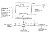
- FIG. 3 shows a simplified schematic view of a plating cell 300 capable of chemical plating according to an embodiment described herein.
- a specific example of an applicable plating station is a cell available on an ElectraTM Cu ECP system, available from Applied Materials, Inc., located in Santa Clara, Calif.
- a detailed description of the deposition system is provided in commonly assigned and co-pending U.S. patent application Ser. No. 09/289,074, entitled “Electro-chemical Deposition System”, filed on Apr. 8, 1999, which is incorporated by reference herein.
- the plating cell 300 includes a power supply 302 , anode 304 , and a substrate support member 305 having a substrate 306 to be plated disposed thereon.
- the power supply 302 is connectable to both the anode 304 and the substrate 306 . More particularly, the power supply 302 is connectable to the substrate 306 via a conductive seed layer formed on a plating surface of the substrate 306 . As such, the substrate 306 acts as a cathode.
- the plating cell 300 may also include a heating member 310 disposed within a wall of the plating cell 300 so not to be in direct contact with the electrolyte solution.
- the heating member 310 adjusts the temperature of the substrate 306 and/or the electrolyte to further enhance the deposition.
- the heating member 310 may be a resistive heating element or may include a heat transfer medium that circulates within one or more channels to transfer energy to the electrolyte solution within the plating cell 300 .
- the heating member 310 may be disposed within the plating cell 300 , in direct contact with the electrolyte solution.
- the heating member 310 may be disposed within the substrate support member 305 to conductively heat the substrate 306 disposed thereon.
- the plating cell 300 is also in fluid communication with a vacuum source 320 , an electrolyte source 330 , and an atmospheric vent 340 .
- the vacuum source 320 is connectable to the plating cell 300 via a conduit 325 .
- the conduit 325 includes an isolation valve 322 to provide an open/close capability between the vacuum source 320 and the plating cell 300 .
- the atmospheric vent 340 is connectable to the plating cell 300 via its own conduit 345 .
- the conduit 345 includes an isolation valve 344 to provide an open/close capability between the atmospheric vent 340 and the plating cell 300 .
- the electrolyte source 330 is connectable to the plating cell 300 via a conduit 335 having an isolation valve 333 disposed therein to provide an open/close capability between the electrolyte source 330 and the plating cell 300 .
- a pressurized inert gas such as nitrogen, may be used to push the electrolyte solution from the electrolyte source 330 to the plating cell 300 and maintain the pressure of the plating cell 300 .
- the desired pressure within the plating cell 300 may be maintained using a pressure regulator/controller 360 in fluid communication with the pressurized inert gas source 362 .
- the pressure regulator may be tied to a feed back loop in communication with a controller 140 , and can be variably controlled to vary/pulsate the pressure within the plating cell 300 .
- each conduit 325 , 335 , and 345 may be individually connected to the plating cell 300 .
- each conduit 325 , 335 , and 345 may be in fluid communication with the plating cell 300 via a single conduit 315 as shown in FIG. 3.
- the conduit 315 is disposed on a lower portion of the plating cell 300 and includes its own isolation valve 311 and also includes a splitter or tee 349 , as is commonly known in the art, to provide a connection to each conduit 325 , 335 , and 345 .
- a substrate 306 having one or more structures formed thereon is disposed in an empty plating cell 300 and the plating cell 300 is sealed while all four isolation valves 311 , 322 , 333 , and 343 are closed.
- the one or more structures formed on the substrate have aspect ratios between about 4:1 to about 10:1, and more preferably, greater than about 10:1.
- the valve 322 is closed and the valve 333 is opened to fill the plating cell 300 with the electrolyte solution, thereby pressurizing the plating cell 300 .
- the pressure of the plating cell 300 is maintained between about 100 mtorr and about 200 atm using the pressure regulator 360 in fluid communication with the source of pressurized inert gas 362 .
- the pressurized plating cell 300 forces the electrolyte solution in the structures formed on the substrate 306 and also collapses any gas pockets/bubbles formed in the electrolyte during the fill step.
- the power supply 302 is activated to provide an electrical current or bias to the anode 304 and to the substrate 306 .
- the bias typically ranges from about ⁇ 15 volts to about 15 volts.
- the positive bias ranges from about 0.1 volts to about 10 volts and the negative bias ranges from about ⁇ 0.1 to about 10 volts.
- the bias may be a current density between about 0.01 and about 40 milliamps/cm 2 for a 200 mm substrate.
- the bias may be varied in power and application depending on the user requirements for plating material to the substrate surface.
- the bias may also be applied by an electrical pulse modulation technique, which applies a constant current density or voltage for a first time period, then applies a constant reverse current density or voltage for a second time period, and repeats the first and second steps, as is described in co-pending U.S. patent application Ser. No. 09/569,833, entitled “Electrochemical Deposition For High Aspect Ratio Structures Using Electrical Pulse Modification”, filed on Dec. 7, 1999, which is incorporated by reference herein.
- a bias voltage is applied to the substrate prior to introduction of the electrolyte in order to prevent etching of the seed layer.
- the plating cell 300 may include one or more ultrasonic transducers 380 disposed therein.
- the one or more transducers 380 are activated to agitate the electrolyte within the plating cell 300 using ultrasonic energy in a range of about 10 Watts to about 250 Watts at a frequency of about 25 kHz to about 200 kHz.
- ultrasonic energy is launched at about 10W to about 100W at a frequency greater than about 40 kHz.
- the one or more ultrasonic transducers 380 are activated at about the same or substantially the same time as the power source 302 is activated. As stated above, the ultrasonic agitation helps to reduce the hydrodynamic boundary layer near the substrate surface to enhance the effects of electrolyte and additives.
- the power supply 302 and the one or more transducers 380 are de-energized.
- the valve 333 is closed and the valve 322 is opened to evacuate/drain the electrolyte solution from the plating cell 300 .
- the valve 322 is closed and the valve 344 is opened to vent the plating cell 300 .
- the plating cell 300 is opened and the plated substrate 306 is removed.
- the electrolyte solution is preferably a copper chemical plating solution having multi-components comprising copper electrolyte and additives such as suppressers and brighteners/accelerators.
- additives such as suppressers and brighteners/accelerators.
- a detailed description of the chemical plating chemistry, particularly the composition of the electrolyte and additives, is provided in commonly assigned and co-pending U.S. patent application Ser. No. 09/245,780, entitled “Electrodeposition Chemistry for Improved Filling of Apertures,” filed on Feb. 5, 1999, which is incorporated by reference herein.
- the copper electrolyte provides copper ions to be deposited while the suppressers and brighteners/accelerators control the deposition profile of the copper atoms.
- Suppressers and brighteners/accelerators adsorb on the substrate surfaces, including the structures formed on the substrate (i.e., vias and trenches), as soon as the substrate comes into contact with the chemical plating bath.
- Suppressers inhibit or reduce copper deposition in areas where suppressers have been adsorbed, and brighteners/accelerators accelerate copper growth in the areas where brighteners/accelerators have been adsorbed.
- the activities of suppressers and brighteners/accelerators are dependent on parameters such as temperature, the pH of bath, and the chloride concentration in the bath, which directly or indirectly affect the polarization of the additives.
- a controller 140 comprising a central processing unit (CPU) 142 , memory 144 , and support circuits 146 , is connected to the plating cell 300 .
- the CPU 142 may be one of any form of computer processors that are used in industrial settings.
- the memory 144 is connected to the CPU 142 , and may be one or more readily available memory devices, such as random access memory (RAM), read only memory (ROM), floppy disk, hard disk, or any other form of digital storage, whether local or remote.
- Software instructions and data can be coded and stored within the memory 144 for instructing the CPU 142 .
- the support circuits 146 are also connected to the CPU 142 for supporting the processor 142 in a conventional manner.
- the support circuits 146 may include cache, power supplies, clock circuits, input/output circuitry, subsystems, and the like.
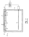
- FIG. 4 shows an alternative embodiment of maintaining and controlling pressure and temperature within a simplified schematic view of a plating cell 400 .
- the plating cell 400 represents an exemplary “face up” plating arrangement and includes similar components to the plating cell 300 shown in FIG. 3 that are identified using identical reference numerals.
- the plating cell 400 includes a piston member 410 at least partially disposed therein.
- the piston member 410 is moveable in a direction substantially normal to the substrate surface.
- the piston member 410 compresses the electrolyte solution in contact with the substrate surface, thereby increasing the pressure of the solution.
- the piston member 410 may move both in a direction toward the substrate surface and in a direction away from the substrate surface to compress and release pressure on the electrolyte solution. This movement of the piston member 410 pulsates the electrolyte solution against the substrate surface.
- a barrier layer having a thickness of about 250 ⁇ and comprising TaN is deposited over a substrate having an aspect ratio of about 10:1 utilizing well known processing parameters for physical vapor deposition.
- the barrier layer is deposited using a Vectra® IMP chamber from Applied Materials, Inc., located in Santa Clara, Calif.
- a copper seed layer of about 2,000 ⁇ is deposited over the barrier layer, also utilizing well known processing parameters for physical vapor deposition.
- the substrate is then transferred to a chemical plating cell, such as one found on the ElectraTM Cu ECP system, available from Applied Materials, Inc., located in Santa Clara, Calif.
- the cell is evacuated by pulling vacuum to about 1 mtorr for about 10 seconds. Bias voltage is applied to the substrate. Electrolyte solution is introduced into the cell until the substrate is at least partially submersed in the electrolyte.
- the electrolyte solution is composed of 0.85M copper sulfate with a pH of about 1.75 after adding suppressers and brighteners/accelerators.
- the cell is then pressurized to about 200 atm. The temperature of the bath is maintained between about 25° C. and about 100° C. during plating.
- the substrate is biased with a forward plating current density between about 10 mA/cm 2 and about 40 mA/cm 2 for a duration between about 4 seconds and about 16 seconds, and a reverse constant voltage of about ⁇ 20V for about 0.3 seconds.
- the cycle is repeated for a total of six times to complete the deposition process.
- the cell is then drained, the power supply is de-energized, and the cell is allowed to vent. Finally, the cell is opened and the plated substrate is removed.
- a barrier layer having a thickness of about 250 ⁇ and comprising TaN is deposited over a substrate having an aspect ratio of about 10:1 utilizing well known processing parameters for physical vapor deposition.
- the barrier layer is deposited using a Vectra® IMP chamber from Applied Materials, Inc., located in Santa Clara, Calif.
- a copper seed layer of about 2,000 ⁇ is deposited over the barrier layer, also utilizing well known processing parameters for physical vapor deposition.
- the substrate is then transferred to a chemical plating cell, such as one found on the ElectraTM Cu ECP system, available from Applied Materials, Inc., located in Santa Clara, Calif.
- the chemical plating cell is evacuated by pulling vacuum to about 1 mtorr for about 10 seconds. Bias voltage is applied to the substrate. Electrolyte solution is introduced into the cell until the substrate is at least partially submersed in the electrolyte.
- the electrolyte solution is composed of 0.85M copper sulfate with a pH of about 1.75 after adding suppressers and brighteners/accelerators.
- the cell is then pressurized to about 200 atm. The temperature of the bath is maintained between about 25° C. and about 100° C. during plating.
- the pressure of the cell is decreased to about 0.5 atm and held between about 1 to about 30 seconds. Then, the pressure is increased back to about 200 atm and held between about 1 and about 30 seconds. This cycle is repeated from about 1 to 50 times before draining the cell, venting the cell, and removing the substrate.
Abstract
A method for chemical plating a substrate is provided. Embodiments of the method include evacuating an enclosure having a substrate disposed therein under vacuum, filling the enclosure with an electrolyte solution having a pressure between about 0.5 atm and about 200 atm, chemical plating a metal layer on a surface of the substrate, and draining the electrolyte solution from the enclosure. In another aspect, the method includes energizing an ultrasonic source to agitate the electrolyte solution substantially simultaneous with the step of chemical plating a metal layer on a surface of the substrate. In still another aspect, the method includes varying the pressure of the plating cell to agitate the electrolyte solution. In yet another aspect, the method includes increasing a pressure of the electrolyte solution by heating the electrolyte solution.
Description
- 1. Field of the Invention
- Embodiments of the present invention relate to a method for chemical plating. More particularly, embodiments of the present invention relate to a method for chemically depositing metals into high aspect ratio structures on a substrate.
- 2. Description of the Related Art
- Reliably producing sub-half micron and smaller structures is one of the key technologies for the next generation of very large scale integration (VLSI) and ultra large-scale integration (ULSI) of semiconductor devices. The shrinking dimensions of interconnects in VLSI and ULSI technology have placed additional demands on the processing capabilities as the limits of circuit technology are pushed. Therefore, reliable formation of these interconnects is important to VLSI and ULSI success and to the continued effort to increase circuit density and quality of individual substrates.
- As circuit densities increase, the widths of vias, contacts and other structures tend to decrease while the thickness of the dielectric layers remains substantially constant. As a result, the aspect ratios for the structures, i.e., the height divided by width, increases. The increasing aspect ratios present a challenge to the industry since many traditional deposition processes, such as physical vapor deposition (PVD) and chemical vapor deposition (CVD), have difficulty filling structures where the aspect ratio exceeds 4:1, and particularly where it exceeds 10:1. Therefore, there is an ongoing effort directed toward the formation of void-free, nanometer-sized structures having high aspect ratios of 4:1 or higher.
- Electrochemical plating (ECP) is one method of metal deposition onto structures having high aspect ratios. FIG. 1 shows a cross section view of a simplified ECP bath used for
semiconductor substrates 10. Generally, theplating bath 10 includes anelectrolyte container 12 having a top opening, asubstrate holder 14 disposed above theelectrolyte container 12, ananode 16 disposed at a bottom portion of theelectrolyte container 12 and acontact ring 20 contacting thesubstrate 22. A plurality ofgrooves 24 are formed in the lower surface of thesubstrate holder 14. A vacuum pump (not shown) is coupled to thesubstrate holder 14 and communicates with thegrooves 24 to create a vacuum condition capable of securing thesubstrate 22 to thesubstrate holder 14 during processing. Thecontact ring 20 comprises a plurality of metallic orsemi-metallic contact pins 26 distributed about the peripheral portion of thesubstrate 22 to define a central substrate plating surface. The plurality ofcontact pins 26 extend radially inwardly over a narrow perimeter portion of thesubstrate 22 and contact a conductive seed layer of thesubstrate 22 at the tips of thecontact pins 26. Apower supply 30 is electrically connected to theanode 16 and to thepins 26 thereby providing an electrical bias to thesubstrate 22. Thesubstrate 22 is positioned above thecylindrical electrolyte container 12 and the electrolyte flow impinges perpendicularly on the substrate plating surface during operation of theplating cell 10. - The electroplating process is typically carried out by applying a constant current density across the substrate plating surface. For example, a constant current density of about 40 mA/cm 2 is applied across the substrate plating surface to produce deposition thereon. Since the deposition rate is generally a function of the current density applied over the substrate plating surface, the current density is typically increased, typically greater than 40 mA/cm2, to provide faster deposition and increase throughput.
- Electroless chemical plating is another method of metal deposition onto structures having high aspect ratios. Electroless chemical plating differs from a typical electrochemical plating process, as described above, in that an electroless chemical plating process does not utilize electrical current. Therefore, no power source, cathode, or electrical contact to a substrate is required.
- A particular problem encountered in any typical chemical plating process, such as ECP and electroless chemical plating, is the inability to provide void-free or seam-free fill of high aspect ratio structures. FIG. 2 illustrates a typical deposition result of a high aspect ratio feature on a
substrate 200. As shown, the mouth/opening 206 of thestructure 202 closes off due to an overhang or excess deposition of metal, because the deposition ofmetal 210 tends to grow faster at the mouth or opening of the structure. As a result, the mouth/opening of the structure is closed off and avoid 204 is formed inside thestructure 202. Furthermore, the overhang or excess deposition of metal is accelerated by an increase of the current density during electroplating, thereby causing even larger voids. - There is a need, therefore, for a method for chemically depositing a metal into high aspect ratio structures on a substrate that provides void-free or seam-free fill of high aspect ratio structures.
- A method for chemical plating is provided. In one aspect, the method includes evacuating an enclosure having a substrate disposed therein to a pressure less than about 1 atm; filling the enclosure with an electrolyte solution at a pressure between about 0.5 atm and about 200 atm; and chemical plating a metal layer on at least a portion of a surface of the substrate.
- In another aspect, the method includes evacuating an enclosure having a substrate disposed therein under a vacuum sufficient to substantially purge gases from the enclosure; filling the enclosure with a pressurized electrolyte solution; energizing one or more ultrasonic sources disposed within the enclosure to agitate the electrolyte solution; chemical plating a metal layer on a surface of the substrate; and draining the electrolyte solution from the enclosure.
- In still another aspect, the method includes evacuating an enclosure having a substrate disposed therein under vacuum; filling the enclosure with an electrolyte solution having a pressure sufficient to substantially collapse air bubbles in the electrolyte solution; and chemical plating a metal layer on at least a portion of a surface of the substrate.
- In still another aspect, the method includes evacuating an enclosure having a substrate disposed therein under vacuum; filling the enclosure with an electrolyte solution having a pressure sufficient to substantially collapse air bubbles in the electrolyte solution; varying the pressure of the electrolyte solution to agitate the electrolyte solution; and chemical plating a metal layer on a surface of the substrate.
- In yet another aspect, the method includes exposing a substrate surface to a vacuum that is sufficient to substantially remove gases from the substrate surface; exposing the substrate surface to an electrolyte solution; pressurizing the electrolyte solution; and chemical plating a metal layer on at least a portion of the substrate surface.
- In yet another aspect, the method includes exposing a substrate surface to a vacuum that is sufficient to substantially remove gases from the substrate surface; exposing the substrate surface to an electrolyte solution; energizing one or more ultrasonic sources to agitate the electrolyte solution; and chemical plating a metal layer on at least a portion of the substrate surface.
- In yet another aspect, the method includes exposing a substrate surface to a vacuum that is sufficient to substantially remove gases from the substrate surface; exposing the substrate surface to an electrolyte solution; energizing one or more ultrasonic sources to agitate the electrolyte solution; chemical plating a metal layer on at least a portion of the substrate surface at a variable pressure between about 1 atm and about 100 atm; and draining the electrolyte solution from the enclosure.
- In still yet another aspect, the method includes opening a first valve to evacuate an enclosure having a substrate disposed therein; pulling vacuum on the enclosure, closing the first valve and opening a second valve to fill the enclosure with an electrolyte solution; closing the second valve; chemical plating a metal layer on at least a portion of a surface of the substrate; opening the second valve to drain the electrolyte solution from the enclosure; and closing the second valve and opening a fourth valve to vent the enclosure prior to removing the plated substrate from the enclosure.
- So that the manner in which the above recited structures of the present invention are attained and can be understood in detail, a more particular description of the invention, briefly summarized above, may be had by reference to the embodiments thereof which are illustrated in the appended drawings.
- It is to be noted, however, that the appended drawings illustrate only typical embodiments of this invention and are therefore not to be considered limiting of its scope, for the invention may admit to other equally effective embodiments.
- FIG. 1 is a simplified cross section view of a typical electrochemical plating cell.
- FIG. 2 is an enlarged schematic view of a high aspect ratio feature wherein the mouth/opening of the structure closes off due to an overhang or excess deposition of copper at the mouth/opening of the structure.
- FIG. 3 is a simplified schematic view of a chemical plating cell configured to perform embodiments of the invention.
- FIG. 4 is a simplified schematic view of a chemical plating cell configured to perform an alternative embodiment of maintaining and controlling electrolyte solution pressure therein.
- A method for chemically depositing a metal, such as copper for example, into high aspect ratio structures of a substrate surface is provided. Embodiments of the method provide void-free and seam-free fill of the high aspect ratio structures. The term “high aspect ratio structures”, as used herein, may include any via, contact, line, or other interconnect feature having an aspect ratio (height to width ratio) of about 4:1 or greater. A “substrate surface”, as used herein, refers to any substrate surface upon which film processing is performed. For example, a substrate surface may include silicon, silicon oxide, doped silicon, germanium, gallium arsenide, glass, sapphire, and any other materials such as metals, metal alloys, and other conductive materials, depending on the application. In certain applications, such as electroless plating for example, a substrate surface may also include dielectric materials such as silicon dioxide and carbon doped silicon oxides. Unless otherwise distinguished below, the term “chemical plating” refers herein to both electrochemical plating and electroless plating.
- In one aspect, embodiments of the method utilize a vacuum that is sufficient to substantially remove/purge gases from a plating volume having the structures disposed therein. The plating volume is contained within an enclosure, such as a plating cell for example, and is in fluid communication with the substrate surface to be plated. The vacuum may be between about 0.1 mtorr and about 100 mtorr, and is intended quickly evacuate unwanted gases, such as reactive compounds and/or contaminants for example, from the enclosure and from the substrate structures prior to chemical plating. Further, the vacuum allows the plating volume to quickly fill with an electrolyte solution. This rapid fill of electrolyte solution greatly improves the rate of production.
- During plating, the electrolyte solution is maintained at a higher pressure to enhance the plating process. The higher pressure may be maintained using a blanket of pressurized gas, such as an inert gas like nitrogen for example, in fluid communication with the electrolyte solution. Alternatively, the higher pressure may be achieved using mechanical forces to compress the electrolyte solution. For example, a moveable piston member may be disposed in communication with the plating volume having the electrolyte solution disposed therein, and used to compress the electrolyte solution, thereby increasing the pressure of the solution.
- The higher pressure drives the electrolyte solution into the substrate structures to provide a more uniform and consistent deposition. The higher pressure also collapses gas pockets or bubbles that may have formed during the fill of the electrolyte solution into the plating volume. Gas pockets or bubbles are undesirable because they create voids in the plating volume and within the substrate structures that could prevent contact with the electrolyte solution. Additionally, the higher pressure elevates the electrolyte solution temperature without evaporation or boiling to further enhance the plating process.
- The higher pressure of the enclosure should be sufficient to substantially collapse air bubbles or pockets of trapped gases in the electrolyte solution and sufficient to force or push the electrolyte solution into the substrate structures. The higher pressure should also be sufficient to allow increase of the electrolyte solution temperature without evaporating/boiling the electrolyte solution. In one aspect, the higher pressure is between about 1 atm and about 200 atm, and is applied for about 1 second to about 120 seconds or until a desired plating thickness, such as between about 100 angstroms (Å) and about 5,000 Å, is achieved.
- In one aspect, the higher pressure may be varied to enhance the plating process. More particularly, the higher pressure of the enclosure may be varied/throttled anywhere between 100 mtorr and 200 atm. As an example, the higher pressure may be increased every 1 to 30 seconds by about 5 to about 20 percent. As another example, the higher pressure may be decreased by about 20 to about 50 percent over a period of time ranging from about 1 second to about 5 minutes. As yet another aspect, the higher pressure may be alternately increased and decreased by about 20 to about 50 percent over an interval of time ranging from about 1 second to about 5 minutes. These significant changes in pressure create pulsations that force/drive electrolyte solution into the substrate structures to provide a more uniform and consistent deposition.
- In another aspect, ultrasonic vibration/agitation may be used to enhance the plating process. The ultrasonic vibration/agitation may be used alone or in combination with the higher pressure described above. Any conventional generation of ultrasonic agitation may be employed. For example, the ultrasonic agitation may be provided by one or more typical Piezo electric crystal transducers, which are commonly known. The source of ultrasonic agitation may be mounted to any mechanical component of the enclosure, such as to an enclosure wall, support pedestal, anode, and cathode. If more than one transducer is used, the multiple transducers may be mounted on the same or different components.
- The ultrasonic agitation moves the substrate and the surrounding electrolyte solution in both vertical and horizontal directions. The ultrasonic energy allows the metal ions to enter small aspect ratio structures formed on the substrate by increasing the metal ions rate of diffusion. As a result, the metal ions are able to diffuse/travel more easily into and out of the small structures formed within the substrate surfaces.
- It is believed that embodiments of the method described above may apply to any wet processing system, such as electrochemical plating and electroless chemical plating, for example. For simplicity and ease of description, however, embodiments of the invention will be further described below as it relates to electrochemical deposition using a typical plating cell described with reference to FIG. 3.
- FIG. 3 shows a simplified schematic view of a
plating cell 300 capable of chemical plating according to an embodiment described herein. A specific example of an applicable plating station is a cell available on an Electra™ Cu ECP system, available from Applied Materials, Inc., located in Santa Clara, Calif. A detailed description of the deposition system is provided in commonly assigned and co-pending U.S. patent application Ser. No. 09/289,074, entitled “Electro-chemical Deposition System”, filed on Apr. 8, 1999, which is incorporated by reference herein. - The
plating cell 300 includes apower supply 302,anode 304, and asubstrate support member 305 having asubstrate 306 to be plated disposed thereon. Thepower supply 302 is connectable to both theanode 304 and thesubstrate 306. More particularly, thepower supply 302 is connectable to thesubstrate 306 via a conductive seed layer formed on a plating surface of thesubstrate 306. As such, thesubstrate 306 acts as a cathode. - The
plating cell 300 may also include aheating member 310 disposed within a wall of the platingcell 300 so not to be in direct contact with the electrolyte solution. Theheating member 310 adjusts the temperature of thesubstrate 306 and/or the electrolyte to further enhance the deposition. Theheating member 310 may be a resistive heating element or may include a heat transfer medium that circulates within one or more channels to transfer energy to the electrolyte solution within the platingcell 300. Alternatively, theheating member 310 may be disposed within the platingcell 300, in direct contact with the electrolyte solution. Further, theheating member 310 may be disposed within thesubstrate support member 305 to conductively heat thesubstrate 306 disposed thereon. - The
plating cell 300 is also in fluid communication with avacuum source 320, anelectrolyte source 330, and an atmospheric vent 340. Thevacuum source 320 is connectable to theplating cell 300 via aconduit 325. Theconduit 325 includes anisolation valve 322 to provide an open/close capability between thevacuum source 320 and the platingcell 300. The atmospheric vent 340 is connectable to theplating cell 300 via itsown conduit 345. Likewise, theconduit 345 includes anisolation valve 344 to provide an open/close capability between the atmospheric vent 340 and the platingcell 300. - The
electrolyte source 330 is connectable to theplating cell 300 via aconduit 335 having anisolation valve 333 disposed therein to provide an open/close capability between theelectrolyte source 330 and the platingcell 300. A pressurized inert gas, such as nitrogen, may be used to push the electrolyte solution from theelectrolyte source 330 to theplating cell 300 and maintain the pressure of the platingcell 300. The desired pressure within the platingcell 300 may be maintained using a pressure regulator/controller 360 in fluid communication with the pressurizedinert gas source 362. The pressure regulator may be tied to a feed back loop in communication with acontroller 140, and can be variably controlled to vary/pulsate the pressure within the platingcell 300. - In one aspect, each
conduit plating cell 300. However, eachconduit cell 300 via asingle conduit 315 as shown in FIG. 3. Theconduit 315 is disposed on a lower portion of the platingcell 300 and includes itsown isolation valve 311 and also includes a splitter ortee 349, as is commonly known in the art, to provide a connection to eachconduit - During operation, a
substrate 306 having one or more structures formed thereon is disposed in anempty plating cell 300 and the platingcell 300 is sealed while all fourisolation valves cell 300 is sealed with thesubstrate 306 disposed therein, thevalve 311 and thevalve 322 are opened to evacuate gas from the platingcell 300 and from the one or more structures formed on thesubstrate 306, creating a vacuum within the platingcell 300. Next, thevalve 322 is closed and thevalve 333 is opened to fill theplating cell 300 with the electrolyte solution, thereby pressurizing the platingcell 300. The pressure of the platingcell 300 is maintained between about 100 mtorr and about 200 atm using thepressure regulator 360 in fluid communication with the source of pressurizedinert gas 362. Thepressurized plating cell 300 forces the electrolyte solution in the structures formed on thesubstrate 306 and also collapses any gas pockets/bubbles formed in the electrolyte during the fill step. - Next, the
power supply 302 is activated to provide an electrical current or bias to theanode 304 and to thesubstrate 306. The bias typically ranges from about −15 volts to about 15 volts. In one aspect, the positive bias ranges from about 0.1 volts to about 10 volts and the negative bias ranges from about −0.1 to about 10 volts. Alternatively, the bias may be a current density between about 0.01 and about 40 milliamps/cm2 for a 200 mm substrate. The bias may be varied in power and application depending on the user requirements for plating material to the substrate surface. The bias may also be applied by an electrical pulse modulation technique, which applies a constant current density or voltage for a first time period, then applies a constant reverse current density or voltage for a second time period, and repeats the first and second steps, as is described in co-pending U.S. patent application Ser. No. 09/569,833, entitled “Electrochemical Deposition For High Aspect Ratio Structures Using Electrical Pulse Modification”, filed on Dec. 7, 1999, which is incorporated by reference herein. In the case of an acidic electrolyte, a bias voltage is applied to the substrate prior to introduction of the electrolyte in order to prevent etching of the seed layer. - Optionally, the plating
cell 300 may include one or moreultrasonic transducers 380 disposed therein. The one ormore transducers 380 are activated to agitate the electrolyte within the platingcell 300 using ultrasonic energy in a range of about 10 Watts to about 250 Watts at a frequency of about 25 kHz to about 200 kHz. Preferably, ultrasonic energy is launched at about 10W to about 100W at a frequency greater than about 40 kHz. The one or moreultrasonic transducers 380 are activated at about the same or substantially the same time as thepower source 302 is activated. As stated above, the ultrasonic agitation helps to reduce the hydrodynamic boundary layer near the substrate surface to enhance the effects of electrolyte and additives. - Once a desired thickness of the metal layer is achieved, the
power supply 302 and the one ormore transducers 380 are de-energized. Thevalve 333 is closed and thevalve 322 is opened to evacuate/drain the electrolyte solution from the platingcell 300. Then, thevalve 322 is closed and thevalve 344 is opened to vent theplating cell 300. Finally, the platingcell 300 is opened and the platedsubstrate 306 is removed. - The electrolyte solution is preferably a copper chemical plating solution having multi-components comprising copper electrolyte and additives such as suppressers and brighteners/accelerators. A detailed description of the chemical plating chemistry, particularly the composition of the electrolyte and additives, is provided in commonly assigned and co-pending U.S. patent application Ser. No. 09/245,780, entitled “Electrodeposition Chemistry for Improved Filling of Apertures,” filed on Feb. 5, 1999, which is incorporated by reference herein.
- The copper electrolyte provides copper ions to be deposited while the suppressers and brighteners/accelerators control the deposition profile of the copper atoms. Suppressers and brighteners/accelerators adsorb on the substrate surfaces, including the structures formed on the substrate (i.e., vias and trenches), as soon as the substrate comes into contact with the chemical plating bath. Suppressers inhibit or reduce copper deposition in areas where suppressers have been adsorbed, and brighteners/accelerators accelerate copper growth in the areas where brighteners/accelerators have been adsorbed. The activities of suppressers and brighteners/accelerators are dependent on parameters such as temperature, the pH of bath, and the chloride concentration in the bath, which directly or indirectly affect the polarization of the additives.
- To facilitate control of the deposition process, a
controller 140 comprising a central processing unit (CPU) 142,memory 144, and supportcircuits 146, is connected to theplating cell 300. TheCPU 142 may be one of any form of computer processors that are used in industrial settings. Thememory 144 is connected to theCPU 142, and may be one or more readily available memory devices, such as random access memory (RAM), read only memory (ROM), floppy disk, hard disk, or any other form of digital storage, whether local or remote. Software instructions and data can be coded and stored within thememory 144 for instructing theCPU 142. Thesupport circuits 146 are also connected to theCPU 142 for supporting theprocessor 142 in a conventional manner. Thesupport circuits 146 may include cache, power supplies, clock circuits, input/output circuitry, subsystems, and the like. - FIG. 4 shows an alternative embodiment of maintaining and controlling pressure and temperature within a simplified schematic view of a
plating cell 400. The platingcell 400 represents an exemplary “face up” plating arrangement and includes similar components to theplating cell 300 shown in FIG. 3 that are identified using identical reference numerals. Additionally, the platingcell 400 includes a piston member 410 at least partially disposed therein. The piston member 410 is moveable in a direction substantially normal to the substrate surface. In one aspect, the piston member 410 compresses the electrolyte solution in contact with the substrate surface, thereby increasing the pressure of the solution. In another aspect, the piston member 410 may move both in a direction toward the substrate surface and in a direction away from the substrate surface to compress and release pressure on the electrolyte solution. This movement of the piston member 410 pulsates the electrolyte solution against the substrate surface. - Embodiments of the invention will be further illustrated by the following non-limiting, hypothetical examples:
- A barrier layer having a thickness of about 250 Å and comprising TaN is deposited over a substrate having an aspect ratio of about 10:1 utilizing well known processing parameters for physical vapor deposition. Preferably, the barrier layer is deposited using a Vectra® IMP chamber from Applied Materials, Inc., located in Santa Clara, Calif. A copper seed layer of about 2,000 Å is deposited over the barrier layer, also utilizing well known processing parameters for physical vapor deposition. The substrate is then transferred to a chemical plating cell, such as one found on the Electra™ Cu ECP system, available from Applied Materials, Inc., located in Santa Clara, Calif.
- The cell is evacuated by pulling vacuum to about 1 mtorr for about 10 seconds. Bias voltage is applied to the substrate. Electrolyte solution is introduced into the cell until the substrate is at least partially submersed in the electrolyte. The electrolyte solution is composed of 0.85M copper sulfate with a pH of about 1.75 after adding suppressers and brighteners/accelerators. The cell is then pressurized to about 200 atm. The temperature of the bath is maintained between about 25° C. and about 100° C. during plating.
- An ultrasonic transducer mounted to the substrate support pedestal having a power of about 100W at a frequency of 50 kHz, is activated during plating and the substrate is biased using a remote power source. The substrate is biased with a forward plating current density between about 10 mA/cm 2 and about 40 mA/cm2 for a duration between about 4 seconds and about 16 seconds, and a reverse constant voltage of about −20V for about 0.3 seconds. The cycle is repeated for a total of six times to complete the deposition process. The cell is then drained, the power supply is de-energized, and the cell is allowed to vent. Finally, the cell is opened and the plated substrate is removed.
- A barrier layer having a thickness of about 250 Å and comprising TaN is deposited over a substrate having an aspect ratio of about 10:1 utilizing well known processing parameters for physical vapor deposition. Preferably, the barrier layer is deposited using a Vectra® IMP chamber from Applied Materials, Inc., located in Santa Clara, Calif. A copper seed layer of about 2,000 Å is deposited over the barrier layer, also utilizing well known processing parameters for physical vapor deposition. The substrate is then transferred to a chemical plating cell, such as one found on the Electra™ Cu ECP system, available from Applied Materials, Inc., located in Santa Clara, Calif.
- The chemical plating cell is evacuated by pulling vacuum to about 1 mtorr for about 10 seconds. Bias voltage is applied to the substrate. Electrolyte solution is introduced into the cell until the substrate is at least partially submersed in the electrolyte. The electrolyte solution is composed of 0.85M copper sulfate with a pH of about 1.75 after adding suppressers and brighteners/accelerators. The cell is then pressurized to about 200 atm. The temperature of the bath is maintained between about 25° C. and about 100° C. during plating.
- After about 15 seconds, the pressure of the cell is decreased to about 0.5 atm and held between about 1 to about 30 seconds. Then, the pressure is increased back to about 200 atm and held between about 1 and about 30 seconds. This cycle is repeated from about 1 to 50 times before draining the cell, venting the cell, and removing the substrate.
- While the foregoing is directed to embodiments of the present invention, other and further embodiments of the invention may be devised without departing from the basic scope thereof, and the scope thereof is determined by the claims that follow.
Claims (65)
1. A method for chemical plating, comprising:
evacuating an enclosure having a substrate disposed therein to a pressure less than about 1 atm;
filling the enclosure with an electrolyte solution at a pressure between about 0.5 atm and about 200 atm; and
chemical plating a metal layer on at least a portion of a surface of the substrate.
2. The method of claim 1 , further comprising energizing one or more ultrasonic sources disposed within the enclosure to agitate the electrolyte solution.
3. The method of claim 1 , further comprising draining the electrolyte solution from the enclosure and venting the enclosure.
4. The method of claim 1 , wherein the enclosure has a variable operating pressure between about 0.5 atm and about 200 atm.
5. The method of claim 1 , wherein chemical plating of a metal layer on a surface of the substrate occurs at a temperature between about 15° C. and about 100° C.
6. The method of claim 1 , further comprising one or more ultrasonic sources disposed within the enclosure to agitate the substrate.
7. The method of claim 1 , wherein evacuating an enclosure comprises removing reactive compounds, contaminants, or both from the enclosure.
8. The method of claim 1 , further comprising varying the pressure to agitate the electrolyte solution.
9. The method of claim 8 , wherein varying the pressure of the electrolyte solution comprises increasing the pressure by about 5 to about 20 percent every 1 to about 30 seconds.
10. The method of claim 8 , wherein varying the pressure of the electrolyte solution comprises decreasing the pressure by about 5 to about 20 percent every 1 to about 30 seconds.
11. The method of claim 1 , further comprising energizing a power source connected to the substrate.
12. A method for chemical plating, comprising:
opening a first valve to evacuate an enclosure having a substrate disposed therein,
pulling vacuum on the enclosure;
closing the first valve and opening a second valve to fill the enclosure with an electrolyte solution;
closing the second valve;
chemical plating a metal layer on at least a portion of a surface of the substrate;
opening the second valve to drain the electrolyte solution from the enclosure; and
closing the second valve and opening a fourth valve to vent the enclosure prior to removing the plated substrate from the enclosure.
13. The method of claim 12 , further comprising energizing one or more ultrasonic sources disposed within the enclosure to agitate the electrolyte solution.
14. The method of claim 12 , further comprising one or more ultrasonic sources disposed within the enclosure to agitate the substrate.
15. The method of claim 12 , wherein chemical plating occurs at pressure of about 0.5 atm to about 200 atm.
16. The method of claim 12 , wherein chemical plating occurs at a temperature of about 15° C. to about 100° C.
17. The method of claim 15 , further comprising varying the pressure to agitate the electrolyte solution in fluid contact with the substrate surface.
18. The method of claim 17 , wherein varying the pressure of the electrolyte solution comprises increasing the pressure by about 5 to about 20 percent every 1 to about 30 seconds.
19. The method of claim 17 , wherein varying the pressure of the electrolyte solution comprises decreasing the pressure by about 5 to about 20 percent every 1 to about 30 seconds.
20. The method of claim 18 , wherein increasing the pressure comprises increasing a temperature of the electrolyte solution to enhance the chemical plating.
21. The method of claim 12 , further comprising energizing a power source connected to the substrate.
22. A method for chemical plating, comprising:
evacuating an enclosure having a substrate disposed therein under a vacuum sufficient to substantially purge gases from the enclosure;
filling the enclosure with a pressurized electrolyte solution;
energizing one or more ultrasonic sources disposed within the enclosure to agitate the electrolyte solution;
chemical plating a metal layer on a surface of the substrate; and
draining the electrolyte solution from the enclosure.
23. The method of claim 22 , further comprising venting the enclosure prior to draining the electrolyte solution from the enclosure.
24. The method of claim 22 , wherein chemical plating occurs at a variable operating pressure between about 100 mtorr and about 200 atm.
25. The method of claim 22 , wherein chemical plating occurs at a temperature of about 15° C. to about 25° C.
26. The method of claim 22 , further comprising energizing one or more ultrasonic sources disposed within the enclosure to agitate the substrate.
27. The method of claim 26 , wherein the substrate is agitated in both a vertical and horizontal direction.
28. The method of claim 22 , wherein the pressurized electrolyte solution has a pressure between about 1 atm and about 200 atm.
29. The method of claim 22 , further comprising varying the pressure of the electrolyte solution to agitate the electrolyte solution.
30. The method of claim 29 , wherein varying the pressure of the electrolyte solution comprises increasing the pressure by about 5 to about 20 percent every 1 to about 30 seconds.
31. The method of claim 29 , wherein varying the pressure of the electrolyte solution comprises decreasing the pressure by about 5 to about 20 percent every 1 to about 30 seconds.
32. The method of claim 30 , wherein increasing the pressure increases a temperature of the electrolyte solution.
33. The method of claim 22 , further comprising energizing a power source connected to the substrate.
34. A method for chemical plating, comprising:
evacuating an enclosure having a substrate disposed therein under vacuum;
filling the enclosure with an electrolyte solution having a pressure sufficient to substantially collapse air bubbles in the electrolyte solution; and
chemical plating a metal layer on at least a portion of a surface of the substrate.
35. The method of claim 34 , further comprising energizing one or more ultrasonic sources to agitate the electrolyte solution.
36. The method of claim 35 , wherein the one or more ultrasonic sources are disposed within the chamber.
37. The method of claim 35 , wherein the one or more ultrasonic sources are adapted to agitate a substrate disposed within the enclosure.
38. The method of claim 34 , further comprising energizing a power source connected to the substrate.
39. The method of claim 34 , further comprising varying the pressure of the electrolyte solution to agitate the electrolyte solution.
40. The method of claim 39 , wherein varying the pressure of the electrolyte solution comprises increasing the pressure by about 5 to about 20 percent every 1 to about 30 seconds.
41. The method of claim 39 , wherein varying the pressure of the electrolyte solution comprises decreasing the pressure by about 5 to about 20 percent every 1 to about 30 seconds.
42. A method for chemical plating, comprising:
evacuating an enclosure having a substrate disposed therein under vacuum;
filling the enclosure with an electrolyte solution having a pressure sufficient to substantially collapse air bubbles in the electrolyte solution;
varying the pressure of the electrolyte solution to agitate the electrolyte solution; and
chemical plating a metal layer on a surface of the substrate.
43. The method of claim 42 , further comprising energizing one or more ultrasonic sources to agitate the electrolyte solution.
44. The method of claim 43 , wherein the one or more ultrasonic sources are disposed within the chamber.
45. The method of claim 42 , further comprising energizing a power source connected to the substrate.
46. The method of claim 42 , wherein varying the pressure of the electrolyte solution comprises increasing the pressure by about 5 to about 20 percent every 1 to about 30 seconds.
47. The method of claim 42 , wherein varying the pressure of the electrolyte solution comprises decreasing the pressure by about 5 to about 20 percent every 1 to about 30 seconds.
48. The method of claim 42 , wherein varying the pressure of the electrolyte solution comprises increasing the pressure by about 5 to about 20 percent every 1 to about 30 seconds followed by decreasing the pressure by about 5 to about 20 percent every 1 to about 30 seconds.
49. A method for chemical plating, comprising:
exposing a substrate surface to a vacuum that is sufficient to substantially remove gases from the substrate surface;
exposing the substrate surface to an electrolyte solution;
energizing one or more ultrasonic sources to agitate the electrolyte solution;
chemical plating a metal layer on at least a portion of the substrate surface at a variable pressure between about 1 atm and about 100 atm; and
draining the electrolyte solution from the enclosure.
50. A method for chemical plating, comprising:
exposing a substrate surface to a vacuum that is sufficient to substantially remove gases from the substrate surface;
exposing the substrate surface to an electrolyte solution;
pressurizing the electrolyte solution; and
chemical plating a metal layer on at least a portion of the substrate surface.
51. The method of claim 50 , wherein pressurizing the electrolyte solution comprises increasing the pressure by about 5 to about 20 percent every 1 to about 30 seconds.
52. The method of claim 50 , further comprising decreasing the pressure of the electrolyte solution by about 5 to about 20 percent every 1 to about 30 seconds.
53. The method of claim 50 , wherein pressurizing the electrolyte solution comprises increasing the pressure by about 5 to about 20 percent every 1 to about 30 seconds followed by decreasing the pressure by about 5 to about 20 percent every 1 to about 30 seconds.
54. The method of claim 50 , wherein pressurizing the electrolyte solution increases a temperature of the electrolyte solution.
55. The method of claim 50 , further comprising compressing the electrolyte solution using a piston member.
56. The method of claim 55 , wherein compressing the electrolyte solution using a piston member pulsates the electrolyte solution across the substrate surface.
57. The method of claim 50 , further comprising energizing one or more ultrasonic sources to agitate the electrolyte solution.
58. The method of claim 50 , further comprising draining the electrolyte solution from the enclosure.
59. A method for chemical plating, comprising:
exposing a substrate surface to a vacuum that is sufficient to substantially remove gases from the substrate surface;
exposing the substrate surface to an electrolyte solution;
energizing one or more ultrasonic sources to agitate the electrolyte solution; and
chemical plating a metal layer on at least a portion of the substrate surface.
60. The method of claim 59 , further comprising compressing the electrolyte solution using a piston member.
61. The method of claim 59 , further comprising pressurizing the electrolyte solution by increasing the pressure by about 5 to about 20 percent every 1 to about 30 seconds.
62. The method of claim 59 , further comprising varying a pressure of the electrolyte solution by increasing the pressure by about 5 to about 20 percent every 1 to about 30 seconds followed by decreasing the pressure by about 5 to about 20 percent every 1 to about 30 seconds.
63. The method of claim 59 , further comprising increasing a pressure of the electrolyte solution by heating the electrolyte solution.
64. The method of claim 59 , further comprising increasing a pressure of the electrolyte solution by heating the substrate surface.
65. The method of claim 63 , wherein the electrolyte solution is heated by the substrate surface.
Priority Applications (1)
| Application Number | Priority Date | Filing Date | Title |
|---|---|---|---|
| US10/128,901 US20030196901A1 (en) | 2002-04-23 | 2002-04-23 | Method for plating metal onto wafers |
Applications Claiming Priority (1)
| Application Number | Priority Date | Filing Date | Title |
|---|---|---|---|
| US10/128,901 US20030196901A1 (en) | 2002-04-23 | 2002-04-23 | Method for plating metal onto wafers |
Publications (1)
| Publication Number | Publication Date |
|---|---|
| US20030196901A1 true US20030196901A1 (en) | 2003-10-23 |
Family
ID=29215531
Family Applications (1)
| Application Number | Title | Priority Date | Filing Date |
|---|---|---|---|
| US10/128,901 Abandoned US20030196901A1 (en) | 2002-04-23 | 2002-04-23 | Method for plating metal onto wafers |
Country Status (1)
| Country | Link |
|---|---|
| US (1) | US20030196901A1 (en) |
Cited By (11)
| Publication number | Priority date | Publication date | Assignee | Title |
|---|---|---|---|---|
| US20040115340A1 (en) * | 2001-05-31 | 2004-06-17 | Surfect Technologies, Inc. | Coated and magnetic particles and applications thereof |
| US20040206628A1 (en) * | 2003-04-18 | 2004-10-21 | Applied Materials, Inc. | Electrical bias during wafer exit from electrolyte bath |
| WO2005076977A2 (en) * | 2004-02-04 | 2005-08-25 | Surfect Technologies, Inc. | Plating apparatus and method |
| US20060011487A1 (en) * | 2001-05-31 | 2006-01-19 | Surfect Technologies, Inc. | Submicron and nano size particle encapsulation by electrochemical process and apparatus |
| US20060078709A1 (en) * | 2004-10-07 | 2006-04-13 | Lue Brian C | Process for controlling wettability of electrochemical plating component surfaces |
| US20080271995A1 (en) * | 2007-05-03 | 2008-11-06 | Sergey Savastiouk | Agitation of electrolytic solution in electrodeposition |
| US20090078575A1 (en) * | 2006-06-05 | 2009-03-26 | State Educational Institution Of Higher Professional Education "Tomsk State Un | Method for vacuum-compression micro plasma oxidation and device for carrying out said method |
| US20090145774A1 (en) * | 2007-12-08 | 2009-06-11 | Comsats Institute Of Information Technology | Novel Sonoelectrolysis for Metal Removal |
| US20100243467A1 (en) * | 2006-04-06 | 2010-09-30 | Daniel Michelet | Surface-active conditional inhibitors for the electroplating of copper on a surface |
| US20100300887A1 (en) * | 2009-06-02 | 2010-12-02 | The Government Of The United States Of America, As Represented By The Secretary Of The Navy | Preparing Electrodes for Electroplating |
| US20110155578A1 (en) * | 2005-04-22 | 2011-06-30 | Renesas Electronics Corporation | Plating process and manufacturing process for semiconductor device thereby |
-
2002
- 2002-04-23 US US10/128,901 patent/US20030196901A1/en not_active Abandoned
Cited By (20)
| Publication number | Priority date | Publication date | Assignee | Title |
|---|---|---|---|---|
| US20040115340A1 (en) * | 2001-05-31 | 2004-06-17 | Surfect Technologies, Inc. | Coated and magnetic particles and applications thereof |
| US20060011487A1 (en) * | 2001-05-31 | 2006-01-19 | Surfect Technologies, Inc. | Submicron and nano size particle encapsulation by electrochemical process and apparatus |
| US20040206628A1 (en) * | 2003-04-18 | 2004-10-21 | Applied Materials, Inc. | Electrical bias during wafer exit from electrolyte bath |
| WO2005076977A2 (en) * | 2004-02-04 | 2005-08-25 | Surfect Technologies, Inc. | Plating apparatus and method |
| US20050230260A1 (en) * | 2004-02-04 | 2005-10-20 | Surfect Technologies, Inc. | Plating apparatus and method |
| WO2005076977A3 (en) * | 2004-02-04 | 2008-09-25 | Surfect Technologies Inc | Plating apparatus and method |
| US20060078709A1 (en) * | 2004-10-07 | 2006-04-13 | Lue Brian C | Process for controlling wettability of electrochemical plating component surfaces |
| US8512540B2 (en) * | 2005-04-22 | 2013-08-20 | Renesas Electronics Corporation | Plating process and manufacturing process for semiconductor device thereby |
| US20110155578A1 (en) * | 2005-04-22 | 2011-06-30 | Renesas Electronics Corporation | Plating process and manufacturing process for semiconductor device thereby |
| US20100243467A1 (en) * | 2006-04-06 | 2010-09-30 | Daniel Michelet | Surface-active conditional inhibitors for the electroplating of copper on a surface |
| US20090078575A1 (en) * | 2006-06-05 | 2009-03-26 | State Educational Institution Of Higher Professional Education "Tomsk State Un | Method for vacuum-compression micro plasma oxidation and device for carrying out said method |
| US8163156B2 (en) * | 2006-06-05 | 2012-04-24 | Tomsk State University (Tsu) | Method for vacuum-compression micro plasma oxidation |
| US20080271995A1 (en) * | 2007-05-03 | 2008-11-06 | Sergey Savastiouk | Agitation of electrolytic solution in electrodeposition |
| US20090145774A1 (en) * | 2007-12-08 | 2009-06-11 | Comsats Institute Of Information Technology | Novel Sonoelectrolysis for Metal Removal |
| US9340434B2 (en) | 2007-12-08 | 2016-05-17 | Comsats Institute Of Information Technology | Recovery of nickel from industrial pickling acid solutions |
| US9512012B2 (en) * | 2007-12-08 | 2016-12-06 | Comsats Institute Of Information Technology | Sonoelectrolysis for metal removal |
| US20100300887A1 (en) * | 2009-06-02 | 2010-12-02 | The Government Of The United States Of America, As Represented By The Secretary Of The Navy | Preparing Electrodes for Electroplating |
| US8404095B2 (en) * | 2009-06-02 | 2013-03-26 | The United States Of America, As Represented By The Secretary Of The Navy | Preparing electrodes for electroplating |
| US20130146467A1 (en) * | 2009-06-02 | 2013-06-13 | The Government of the United States, as represented by the Secretary of the Navy, Naval Re | Preparing Electrodes for Electroplating |
| US8728293B2 (en) * | 2009-06-02 | 2014-05-20 | The United States of America, as represented by the Secretary of the Navy, Naval Research Laboratory | Preparing electrodes for electroplating |
Similar Documents
| Publication | Publication Date | Title |
|---|---|---|
| JP6681953B2 (en) | Method and apparatus for reducing metal oxides on metal seed layers | |
| KR100987835B1 (en) | Method for seed film formation, plasma film forming apparatus, and memory medium | |
| US8026176B2 (en) | Film forming method, plasma film forming apparatus and storage medium | |
| KR102513108B1 (en) | Atmospheric plasma apparatus for semiconductor processing | |
| US8415261B1 (en) | Capping before barrier-removal IC fabrication method | |
| US20030196901A1 (en) | Method for plating metal onto wafers | |
| EP1084512A1 (en) | Plasma treatment for ex-situ contact fill | |
| US9070750B2 (en) | Methods for reducing metal oxide surfaces to modified metal surfaces using a gaseous reducing environment | |
| KR20080080941A (en) | Method for manufacturing semiconductor device, simiconductor manufacturing apparatus and storage medium for executing the method | |
| JP4163728B2 (en) | Electroplating method | |
| US7700484B2 (en) | Method and apparatus for a metallic dry-filling process | |
| US7348266B2 (en) | Method and apparatus for a metallic dry-filling process | |
| US9714474B2 (en) | Seed layer deposition in microscale features | |
| US6123984A (en) | Method and apparatus for plating a substrate | |
| EP1069212A1 (en) | Electrochemical deposition for high aspect ratio structures using electrical pulse modulation | |
| US7618888B2 (en) | Temperature-controlled metallic dry-fill process | |
| KR20110056455A (en) | Film formation method and storage medium | |
| US11203816B1 (en) | Electroplating seed layer buildup and repair | |
| US7312149B2 (en) | Copper plating of semiconductor devices using single intermediate low power immersion step | |
| JP2004006942A (en) | Copper thin film formation method | |
| JPH10265949A (en) | Formation of copper thin film |
Legal Events
| Date | Code | Title | Description |
|---|---|---|---|
| AS | Assignment |
Owner name: APPLIED MATERIALS, INC., CALIFORNIA Free format text: ASSIGNMENT OF ASSIGNORS INTEREST;ASSIGNOR:GRUNES, HOWARD E.;REEL/FRAME:012848/0547 Effective date: 20020423 |
|
| STCB | Information on status: application discontinuation |
Free format text: ABANDONED -- FAILURE TO RESPOND TO AN OFFICE ACTION |