US20030197467A1 - Highly efficient OLEDs using doped ambipolar conductive molecular organic thin films - Google Patents
Highly efficient OLEDs using doped ambipolar conductive molecular organic thin films Download PDFInfo
- Publication number
- US20030197467A1 US20030197467A1 US10/452,659 US45265903A US2003197467A1 US 20030197467 A1 US20030197467 A1 US 20030197467A1 US 45265903 A US45265903 A US 45265903A US 2003197467 A1 US2003197467 A1 US 2003197467A1
- Authority
- US
- United States
- Prior art keywords
- organic
- layer
- characteristic
- light emitting
- emitting device
- Prior art date
- Legal status (The legal status is an assumption and is not a legal conclusion. Google has not performed a legal analysis and makes no representation as to the accuracy of the status listed.)
- Granted
Links
- 239000010409 thin film Substances 0.000 title description 3
- 239000000463 material Substances 0.000 claims abstract description 133
- VFUDMQLBKNMONU-UHFFFAOYSA-N 9-[4-(4-carbazol-9-ylphenyl)phenyl]carbazole Chemical group C12=CC=CC=C2C2=CC=CC=C2N1C1=CC=C(C=2C=CC(=CC=2)N2C3=CC=CC=C3C3=CC=CC=C32)C=C1 VFUDMQLBKNMONU-UHFFFAOYSA-N 0.000 claims description 54
- UEEXRMUCXBPYOV-UHFFFAOYSA-N iridium;2-phenylpyridine Chemical compound [Ir].C1=CC=CC=C1C1=CC=CC=N1.C1=CC=CC=C1C1=CC=CC=N1.C1=CC=CC=C1C1=CC=CC=N1 UEEXRMUCXBPYOV-UHFFFAOYSA-N 0.000 claims description 48
- 239000010406 cathode material Substances 0.000 claims description 8
- 239000010405 anode material Substances 0.000 claims description 5
- FYYHWMGAXLPEAU-UHFFFAOYSA-N Magnesium Chemical compound [Mg] FYYHWMGAXLPEAU-UHFFFAOYSA-N 0.000 claims 2
- 229910052749 magnesium Inorganic materials 0.000 claims 2
- 239000011777 magnesium Substances 0.000 claims 2
- 229910052709 silver Inorganic materials 0.000 claims 2
- 239000004332 silver Substances 0.000 claims 2
- 230000005281 excited state Effects 0.000 abstract description 12
- 239000011368 organic material Substances 0.000 abstract description 4
- 239000010410 layer Substances 0.000 description 77
- DIVZFUBWFAOMCW-UHFFFAOYSA-N 4-n-(3-methylphenyl)-1-n,1-n-bis[4-(n-(3-methylphenyl)anilino)phenyl]-4-n-phenylbenzene-1,4-diamine Chemical compound CC1=CC=CC(N(C=2C=CC=CC=2)C=2C=CC(=CC=2)N(C=2C=CC(=CC=2)N(C=2C=CC=CC=2)C=2C=C(C)C=CC=2)C=2C=CC(=CC=2)N(C=2C=CC=CC=2)C=2C=C(C)C=CC=2)=C1 DIVZFUBWFAOMCW-UHFFFAOYSA-N 0.000 description 34
- 239000002019 doping agent Substances 0.000 description 19
- 230000032258 transport Effects 0.000 description 15
- 230000015572 biosynthetic process Effects 0.000 description 14
- 238000002347 injection Methods 0.000 description 13
- 239000007924 injection Substances 0.000 description 13
- IBHBKWKFFTZAHE-UHFFFAOYSA-N n-[4-[4-(n-naphthalen-1-ylanilino)phenyl]phenyl]-n-phenylnaphthalen-1-amine Chemical group C1=CC=CC=C1N(C=1C2=CC=CC=C2C=CC=1)C1=CC=C(C=2C=CC(=CC=2)N(C=2C=CC=CC=2)C=2C3=CC=CC=C3C=CC=2)C=C1 IBHBKWKFFTZAHE-UHFFFAOYSA-N 0.000 description 12
- 238000000034 method Methods 0.000 description 10
- 230000006798 recombination Effects 0.000 description 10
- 238000005215 recombination Methods 0.000 description 10
- 238000004770 highest occupied molecular orbital Methods 0.000 description 9
- 230000037230 mobility Effects 0.000 description 9
- 239000000758 substrate Substances 0.000 description 9
- 238000004768 lowest unoccupied molecular orbital Methods 0.000 description 8
- 238000000151 deposition Methods 0.000 description 6
- 238000009825 accumulation Methods 0.000 description 4
- 230000005540 biological transmission Effects 0.000 description 4
- 230000000903 blocking effect Effects 0.000 description 4
- 238000005286 illumination Methods 0.000 description 4
- 238000004020 luminiscence type Methods 0.000 description 4
- 238000004519 manufacturing process Methods 0.000 description 4
- 230000003287 optical effect Effects 0.000 description 4
- TVIVIEFSHFOWTE-UHFFFAOYSA-K tri(quinolin-8-yloxy)alumane Chemical compound [Al+3].C1=CN=C2C([O-])=CC=CC2=C1.C1=CN=C2C([O-])=CC=CC2=C1.C1=CN=C2C([O-])=CC=CC2=C1 TVIVIEFSHFOWTE-UHFFFAOYSA-K 0.000 description 4
- 230000008901 benefit Effects 0.000 description 3
- AMGQUBHHOARCQH-UHFFFAOYSA-N indium;oxotin Chemical compound [In].[Sn]=O AMGQUBHHOARCQH-UHFFFAOYSA-N 0.000 description 3
- 239000012044 organic layer Substances 0.000 description 3
- 229920000642 polymer Polymers 0.000 description 3
- 238000002207 thermal evaporation Methods 0.000 description 3
- STTGYIUESPWXOW-UHFFFAOYSA-N 2,9-dimethyl-4,7-diphenyl-1,10-phenanthroline Chemical compound C=12C=CC3=C(C=4C=CC=CC=4)C=C(C)N=C3C2=NC(C)=CC=1C1=CC=CC=C1 STTGYIUESPWXOW-UHFFFAOYSA-N 0.000 description 2
- 229910019015 Mg-Ag Inorganic materials 0.000 description 2
- HCHKCACWOHOZIP-UHFFFAOYSA-N Zinc Chemical compound [Zn] HCHKCACWOHOZIP-UHFFFAOYSA-N 0.000 description 2
- 230000000052 comparative effect Effects 0.000 description 2
- 230000008021 deposition Effects 0.000 description 2
- 238000010586 diagram Methods 0.000 description 2
- 238000001194 electroluminescence spectrum Methods 0.000 description 2
- 238000005566 electron beam evaporation Methods 0.000 description 2
- 238000005516 engineering process Methods 0.000 description 2
- 238000002474 experimental method Methods 0.000 description 2
- 239000011521 glass Substances 0.000 description 2
- 229910052751 metal Inorganic materials 0.000 description 2
- 239000002184 metal Substances 0.000 description 2
- 238000012986 modification Methods 0.000 description 2
- 230000004048 modification Effects 0.000 description 2
- 230000008569 process Effects 0.000 description 2
- 238000010791 quenching Methods 0.000 description 2
- 230000000171 quenching effect Effects 0.000 description 2
- 230000009467 reduction Effects 0.000 description 2
- 239000002356 single layer Substances 0.000 description 2
- 238000012546 transfer Methods 0.000 description 2
- 229910052725 zinc Inorganic materials 0.000 description 2
- 239000011701 zinc Substances 0.000 description 2
- 150000000183 1,3-benzoxazoles Chemical class 0.000 description 1
- ATKYPLNPUMJYCQ-UHFFFAOYSA-N 2-(2-hydroxyphenyl)-3H-1,3-benzothiazole-2-carboxylic acid Chemical compound N1C2=CC=CC=C2SC1(C(=O)O)C1=CC=CC=C1O ATKYPLNPUMJYCQ-UHFFFAOYSA-N 0.000 description 1
- IGFDHFHBTKRPJC-UHFFFAOYSA-N 2-(2-hydroxyphenyl)-3H-1,3-benzoxazole-2-carboxylic acid Chemical compound N1C2=CC=CC=C2OC1(C(=O)O)C1=CC=CC=C1O IGFDHFHBTKRPJC-UHFFFAOYSA-N 0.000 description 1
- FQJQNLKWTRGIEB-UHFFFAOYSA-N 2-(4-tert-butylphenyl)-5-[3-[5-(4-tert-butylphenyl)-1,3,4-oxadiazol-2-yl]phenyl]-1,3,4-oxadiazole Chemical compound C1=CC(C(C)(C)C)=CC=C1C1=NN=C(C=2C=C(C=CC=2)C=2OC(=NN=2)C=2C=CC(=CC=2)C(C)(C)C)O1 FQJQNLKWTRGIEB-UHFFFAOYSA-N 0.000 description 1
- OGGKVJMNFFSDEV-UHFFFAOYSA-N 3-methyl-n-[4-[4-(n-(3-methylphenyl)anilino)phenyl]phenyl]-n-phenylaniline Chemical compound CC1=CC=CC(N(C=2C=CC=CC=2)C=2C=CC(=CC=2)C=2C=CC(=CC=2)N(C=2C=CC=CC=2)C=2C=C(C)C=CC=2)=C1 OGGKVJMNFFSDEV-UHFFFAOYSA-N 0.000 description 1
- OAICVXFJPJFONN-UHFFFAOYSA-N Phosphorus Chemical compound [P] OAICVXFJPJFONN-UHFFFAOYSA-N 0.000 description 1
- 238000004847 absorption spectroscopy Methods 0.000 description 1
- 238000004458 analytical method Methods 0.000 description 1
- 230000004888 barrier function Effects 0.000 description 1
- -1 benzthiazole compound Chemical class 0.000 description 1
- 239000002800 charge carrier Substances 0.000 description 1
- 239000003086 colorant Substances 0.000 description 1
- 150000001875 compounds Chemical class 0.000 description 1
- IOJUPLGTWVMSFF-UHFFFAOYSA-N cyclobenzothiazole Natural products C1=CC=C2SC=NC2=C1 IOJUPLGTWVMSFF-UHFFFAOYSA-N 0.000 description 1
- 230000007423 decrease Effects 0.000 description 1
- 230000003247 decreasing effect Effects 0.000 description 1
- 230000005684 electric field Effects 0.000 description 1
- 238000001017 electron-beam sputter deposition Methods 0.000 description 1
- 230000005284 excitation Effects 0.000 description 1
- 239000010408 film Substances 0.000 description 1
- 230000005525 hole transport Effects 0.000 description 1
- 238000010348 incorporation Methods 0.000 description 1
- 239000003446 ligand Substances 0.000 description 1
- 239000004973 liquid crystal related substance Substances 0.000 description 1
- SJCKRGFTWFGHGZ-UHFFFAOYSA-N magnesium silver Chemical compound [Mg].[Ag] SJCKRGFTWFGHGZ-UHFFFAOYSA-N 0.000 description 1
- 150000002902 organometallic compounds Chemical class 0.000 description 1
- 150000004866 oxadiazoles Chemical class 0.000 description 1
- 150000005041 phenanthrolines Chemical class 0.000 description 1
- 239000004033 plastic Substances 0.000 description 1
- 230000001737 promoting effect Effects 0.000 description 1
- 239000010453 quartz Substances 0.000 description 1
- 230000005855 radiation Effects 0.000 description 1
- 238000012552 review Methods 0.000 description 1
- 229910052594 sapphire Inorganic materials 0.000 description 1
- 239000010980 sapphire Substances 0.000 description 1
- VYPSYNLAJGMNEJ-UHFFFAOYSA-N silicon dioxide Inorganic materials O=[Si]=O VYPSYNLAJGMNEJ-UHFFFAOYSA-N 0.000 description 1
- 239000002904 solvent Substances 0.000 description 1
- 238000001228 spectrum Methods 0.000 description 1
- 238000004528 spin coating Methods 0.000 description 1
- 150000003852 triazoles Chemical class 0.000 description 1
- 238000009736 wetting Methods 0.000 description 1
Images


Classifications
-
- H—ELECTRICITY
- H10—SEMICONDUCTOR DEVICES; ELECTRIC SOLID-STATE DEVICES NOT OTHERWISE PROVIDED FOR
- H10K—ORGANIC ELECTRIC SOLID-STATE DEVICES
- H10K50/00—Organic light-emitting devices
- H10K50/10—OLEDs or polymer light-emitting diodes [PLED]
- H10K50/17—Carrier injection layers
-
- H—ELECTRICITY
- H10—SEMICONDUCTOR DEVICES; ELECTRIC SOLID-STATE DEVICES NOT OTHERWISE PROVIDED FOR
- H10K—ORGANIC ELECTRIC SOLID-STATE DEVICES
- H10K50/00—Organic light-emitting devices
- H10K50/10—OLEDs or polymer light-emitting diodes [PLED]
- H10K50/11—OLEDs or polymer light-emitting diodes [PLED] characterised by the electroluminescent [EL] layers
-
- H—ELECTRICITY
- H10—SEMICONDUCTOR DEVICES; ELECTRIC SOLID-STATE DEVICES NOT OTHERWISE PROVIDED FOR
- H10K—ORGANIC ELECTRIC SOLID-STATE DEVICES
- H10K2101/00—Properties of the organic materials covered by group H10K85/00
- H10K2101/10—Triplet emission
-
- H—ELECTRICITY
- H10—SEMICONDUCTOR DEVICES; ELECTRIC SOLID-STATE DEVICES NOT OTHERWISE PROVIDED FOR
- H10K—ORGANIC ELECTRIC SOLID-STATE DEVICES
- H10K50/00—Organic light-emitting devices
- H10K50/10—OLEDs or polymer light-emitting diodes [PLED]
- H10K50/14—Carrier transporting layers
-
- H—ELECTRICITY
- H10—SEMICONDUCTOR DEVICES; ELECTRIC SOLID-STATE DEVICES NOT OTHERWISE PROVIDED FOR
- H10K—ORGANIC ELECTRIC SOLID-STATE DEVICES
- H10K85/00—Organic materials used in the body or electrodes of devices covered by this subclass
- H10K85/30—Coordination compounds
- H10K85/341—Transition metal complexes, e.g. Ru(II)polypyridine complexes
-
- H—ELECTRICITY
- H10—SEMICONDUCTOR DEVICES; ELECTRIC SOLID-STATE DEVICES NOT OTHERWISE PROVIDED FOR
- H10K—ORGANIC ELECTRIC SOLID-STATE DEVICES
- H10K85/00—Organic materials used in the body or electrodes of devices covered by this subclass
- H10K85/60—Organic compounds having low molecular weight
- H10K85/631—Amine compounds having at least two aryl rest on at least one amine-nitrogen atom, e.g. triphenylamine
-
- Y—GENERAL TAGGING OF NEW TECHNOLOGICAL DEVELOPMENTS; GENERAL TAGGING OF CROSS-SECTIONAL TECHNOLOGIES SPANNING OVER SEVERAL SECTIONS OF THE IPC; TECHNICAL SUBJECTS COVERED BY FORMER USPC CROSS-REFERENCE ART COLLECTIONS [XRACs] AND DIGESTS
- Y10—TECHNICAL SUBJECTS COVERED BY FORMER USPC
- Y10T—TECHNICAL SUBJECTS COVERED BY FORMER US CLASSIFICATION
- Y10T428/00—Stock material or miscellaneous articles
- Y10T428/24—Structurally defined web or sheet [e.g., overall dimension, etc.]
- Y10T428/24942—Structurally defined web or sheet [e.g., overall dimension, etc.] including components having same physical characteristic in differing degree
Definitions
- the present invention relates to highly efficient organic light emitting devices (OLEDs) utilizing doped ambipolar conductive molecular organic thin films.
- OLEDs Organic light emitting devices
- LCDs liquid crystal displays Due to their high luminous efficiencies, electrophosphorescent OLEDs are seen as having the potential to replace incandescent, and perhaps even fluorescent, lamps for certain types of applications.
- Light emission from OLEDs is typically via fluorescence or phosphorescence.
- phosphorescence refers to emission from a triplet excited state of an organic molecule and the term “fluorescence” refers to emission from a singlet excited state of an organic molecule.
- an advantage of phosphorescence is that all excitons (formed by the recombination of holes and electrons in an EL), which are formed either as a singlet or triplet excited state, may participate in luminescence. This is because the lowest singlet excited state of an organic molecule is typically at a slightly higher energy than the lowest triplet excited state. This means that, for typical phosphorescent organometallic compounds, the lowest singlet excited state may rapidly decay to the lowest triplet excited state from which the phosphorescence is produced. In contrast, only a small percentage (about 25%) of excitons in fluorescent devices are capable of producing the fluorescent luminescence that is obtained from a singlet excited state.
- the remaining excitons in a fluorescent device which are produced in the lowest triplet excited state of an organic molecule, are typically not capable of being converted into the energetically unfavorable higher singlet excited states from which the fluorescence is produced. This energy, thus, becomes lost to radiationless decay processes that heat-up the device.
- OLEDs organic light emitting devices
- Ir(ppy) 3 fac tris(2-phenylpyridine)iridium
- the triplet level of the metal-ligand charge transfer state of the green-emitting Ir(ppy) 3 is between 2.5 eV and 3.0 eV
- deep blue fluorophores with a peak wavelength at about 400 nm such as 4,4′-N,N′-dicarbazole-biphenyl (CBP) are likely candidates as triplet energy transfer and exciton confining media.
- CBP 4,4′-N,N′-dicarbazole-biphenyl
- Using 6% to 10%-Ir(ppy) 3 in CBP leads to efficient Ir(ppy) 3 phosphorescence.
- the control of charge carrier injection and transport in the host layers is believed to be necessary for achieving efficient formation of radiative excitons.
- m-MTDATA 4,4′,4′′-tris(3-methylphenylphenylamino)triphenylamine
- electrophosphorescent OLEDs are comprised of several layers so as to achieve the desired combination of OLED performance characteristics. It would be desirable if the desired combination of OLED performance characteristics, especially including high external quantum efficiency, could be achieved used simplified OLED structures that make use of a smaller number of layers.
- the present invention is directed to simplified OLED structures comprising an anode layer, a hole injecting layer (HIL) in direct contact with the anode layer, an emissive electron transporting layer (ETL) in direct contact with the hole injecting layer, and a cathode layer in direct contact with the emissive electron transporting layer.
- the hole injecting material used in the hole injecting layer is characterized, in particular, as being an organic material having an ionization potential (IP) that is not more than about 0.7 eV greater than the ionization potential of the material used for the anode layer.
- the emissive organic electron transporting layer comprises an organic electron transporting material and an organic hole-trapping emissive material, for example, a hole-trapping phosphorescent material.
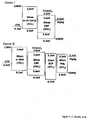
- FIG. 1 shows the energy level diagrams for a representative embodiment of the invention (Device I), as compared with a prior art OLED structure (Device II).
- FIG. 2 shows the external quantum efficiency and power efficiency as a function of the current density for Device I (circles) as compared with Device II (squares).
- FIG. 3 shows the external quantum efficiency as a function of CBP spacer thickness for Device I as compared with Device II.
- FIG. 4 shows the EL intensity as a function of wavelength for Device I as compared with Device II.
- FIG. 5 shows the current density as a function of voltage for Device I as compared with Device II.
- FIG. 6 shows a schematic representation of an OLED structure according to the present invention.
- the simplified OLED structures of the present invention are illustrated and described herein for OLED structures in which the organic hole trapping emissive material is a phosphorescent emissive material, for which the emission is produced from a triplet excited state of an organic molecule.
- the representative embodiments of the present invention are illustrated and described herein as using a phosphorescent organic material as the emissive material in the emissive organic electron transporting layer
- the full scope of the present invention also includes use of a fluorescent material as the emissive material in the emissive electron transporting layer. More specifically, the full scope of the present invention includes OLEDs containing a hole-trapping fluorescent material wherein each of the materials in the OLED may have the combination of properties as described herein.
- FIG. 1 The representative simplified OLED structures of the present invention are illustrated for an electrophosphorescent OLED having the structure ITO/m-MTDATA/CBP:Ir(ppy) 3 /Mg:Ag.
- such a structure corresponds to an OLED structure having an indium tin oxide (ITO) anode layer, an m-MTDATA (4,4′,4′′-tris(3-methylphenylphenylamino)triphenylamine) hole injecting layer in direct contact with the ITO layer, an Ir(ppy) 3 -doped CBP layer in direct contact with the m-MTDATA hole injecting layer, and a magnesium-silver cathode layer in direct contact with the Ir(ppy) 3 -doped CBP layer.
- ITO indium tin oxide
- m-MTDATA (4,4′,4′′-tris(3-methylphenylphenylamino)triphenylamine) hole injecting layer
- Structures having an Ir(ppy) 3 -doped concentration of about 7% in the host CBP layer are disclosed herein to have a peak external quantum ( ⁇ ext ) and power efficiency ( ⁇ p ) of 12.0 ⁇ 0.6% and 45 ⁇ 2 lm/W, respectively. This corresponds to an internal quantum efficiency of about 60%. These efficiencies are believed to be the highest efficiencies yet disclosed for an Ir(ppy) 3 -doped electrophosphorescent OLED.
- the unexpectedly high efficiency of the simplified OLED structures of the present invention may be attributed to the unique combination of properties as exemplified by the representative materials of the present invention, that is, the simplified ITO/m-MTDATA/CBP:Ir(ppy) 3 /Mg:Ag system.
- the simplified OLED structures of the present invention are represented, in particular, by structures in which the emissive, phosphorescent-doped, electron transporting layer is in direct contact with a low work function cathode material.
- the present invention is not limited by any theory about how the invention works, it is believed that the high OLED quantum efficiency is achieved, at least in part, because the representative materials permit direct hole trapping by the phosphorescent dopant material, with subsequent hole/electron recombination taking place directly on the phosphorescent material, which then emits phosphorescent radiation.
- efficient hole trapping by the emissive phosphorescent dopant material makes it unnecessary to have an exciton and/or hole blocking layer between the emissive layer and the cathode layer.
- Such exciton and/or hole blocking layers have typically been used to reduce the hole/electron recombination losses at the cathode interface.
- the efficiency of an OLED may be improved, in some cases, by including a hole blocking layer between the emissive electron transporting layer and the cathode so as to reduce or prevent losses in efficiency that are caused by hole quenching at the cathode.
- the present invention thus, permits fabrication and manufacture of highly efficient electrophosphorescent OLEDs using a reduced number of organic layers.
- the present invention has the further advantage of permitting use of a single layer, which is a hole injecting organic layer, between the anode layer and the emissive electron transport layer.
- the hole injecting materials of the present invention may be characterized as materials that planarize or wet the anode surface so as to provide efficient hole injection from the anode into the hole injecting material.
- the hole injecting materials of the present invention are further characterized as having HOMO (Highest Occupied Molecular Orbital) energy levels that favorably match up, as defined by their herein-described relative IP energies, with the adjacent anode layer on one side of the HIL layer and the phosphorescent-doped electron transporting layer on the opposite side of the HIL.
- HOMO Highest Occupied Molecular Orbital
- the HIL material preferably has an IP not more than about 0.7 eV greater that the IP of the anode material. More preferably, the HIL material has an IP not more than about 0.5 eV greater than the anode material. As shown in FIG. 1, the HIL material m-MTDATA is believed to have an IP (5.1 eV) that is about 0.4 eV greater than the IP of the ITO anode (4.7 eV).
- the HIL materials are further distinguished from conventional hole transporting materials that are typically used in the hole transporting layer of an OLED in that such HIL materials have a hole mobility that is substantially less than the hole mobility of conventional hole transporting materials.
- HTL hole transporting layers
- m-MTDATA has been identified as effective in promoting injection of holes from ITO into hole transporting layers (HTL) consisting of, for example 4,4′-bis[N-(naphthyl)-N-phenyl-amino]biphenyl ( ⁇ -NPD) or N,N′-bis(3-methylphenyl)-N,N′-diphenyl-[1,1′-biphenyl]4,4′-diamine (TPD), possibly due to reduction of the HTL HOMO level/ITO offset energy, or to wetting of the ITO surface.
- HTL hole transporting layers
- the HIL material m-MTDATA is believed to have a hole mobility of about 3 ⁇ 10 ⁇ 5 cm 2 /Vsec as compared with the conventional hole transporting materials such as ⁇ -NPD or TPD, which have a hole mobility of about 5 ⁇ 10 ⁇ 4 cm 2 /Vsec and 9 ⁇ 10 ⁇ 4 cm 2 /Vsec, respectively.
- the m-MTDATA material has a hole mobility more than an order of magnitude less than the commonly used HTL materials ⁇ -NPD and TPD.
- the improved efficiencies of the electrophosphorescent OLEDs of the present invention may result from a combination of properties, it is believed that the reduced hole mobility of the representative HIL material m-MTDATA may help to balance hole and electron injection.
- the hole transporting materials that are typically used in an OLED tend to have substantially higher charge-carrying mobilities for holes than is typical for the electrons in the highest-mobility electron transporting materials, it is believed that the high OLED efficiencies disclosed herein show that it may not be necessary to use hole transporting materials having the highest possible hole mobilities.
- the present invention is further directed to HIL materials having a hole mobility not greater than about 1 ⁇ 10 ⁇ 4 cm 2 /Vsec.
- the thickness of the HIL of the present invention needs to be thick enough to help planarize or wet the surface of the anode layer.
- an HIL thickness of as little as 10 nm may be acceptable for a very smooth anode surface.
- a thickness for the HIL of up to 50 nm may be desired in some cases.
- the host electron transporting material in the ETL may be selected such that electrons can be efficiently injected from the cathode into the LUMO (Lowest Unoccupied Molecular Orbital) level of the electron transporting material.
- the LUMO level of an organic material may be generally characterized by the electron affinity of that material and the relative electron injection efficiently of a cathode may be generally characterized in terms of the work function of the cathode material. This means that the preferred properties of the host ETL material and the electron injecting material may be specified in terms of the electron affinity of the ETL material and the work function of the cathode material.
- the work function of the cathode material is preferably not greater than the electron affinity of the electron transporting material by more than about 0.75 eV, more preferably, by not more than about 0.5 eV.
- the electron affinity of the electron transporting material is greater than the work function of the cathode material.
- the work function of the Mg:Ag cathode (about 3.7 eV) is about 0.7 eV. greater than the electron affinity of the electron transporting material (about 3.0 eV).
- the host electron transporting material preferably has a LUMO level corresponding to an electron affinity that is greater than or equal to the electron affinity of the dopant phosphorescent material, such that electron transport in the electron transporting layer occurs predominantly by electron transport through the LUMO levels of the electron transporting host material.
- the electron affinity of the host electron transporting material is preferably not more than about 0.5 eV greater than the phosphorescent dopant, such that efficient electron injection can readily occur from the host to the dopant, thus resulting in efficient hole/electron recombination directly on the hole-trapping phosphorescent dopant.
- the host electron transporting material has an electron affinity (about 3.0 eV) that is about equal to the electron affinity of the phosphorescent dopant (also about 3.0 eV).
- a hole-trapping phosphorescent material may be characterized as a phosphorescent material having an IP that is approximately the same as or sufficiently less than the IP of the host material, such that holes can be effectively trapped by the phosphorescent dopant.
- the phosphorescent dopant preferably has an IP that is at least about 0.5 eV less than the IP of the host material.
- the electron transporting host material has an IP (6.3 eV) that is about 0.7 eV greater than the IP of the phosphorescent dopant (5.6 eV).
- the phosphorescent dopant material may be characterized as preferably having an IP that is approximately equal, but not necessarily precisely equal, to the IP of the adjacent HIL material.
- IP an IP that is approximately equal, but not necessarily precisely equal, to the IP of the adjacent HIL material.
- the phosphorescent Ir(ppy) 3 -dopant has an IP about 0.5 eV greater than the IP of the adjacent m-MTDATA material.
- the IP of the dopant is preferably not greater than the IP of the HIL material by more than about 0.7 eV.
- the phosphorescent dopant material may be doped into the host electron transporting material at a concentration level so as to achieve the desired combination of OLED performance characteristics, for example, a high initial quantum efficiency, or perhaps alternatively, a high lifetime quantum efficiency.
- the phosphorescent dopant material concentration ranges from about 1 weight percent up to about 10 weight percent, and perhaps up to 20 weight percent or still higher in some cases. Phosphorescent emission from an excited triplet state of an organic molecule is produced when a voltage is applied across the phosphorescent-doped ETL of such an OLED.
- the hole injecting materials, the electron transporting materials and the phosphorescent dopant materials may each be selected from a vast array of materials known in the art, provided that the relative energy levels of these materials, when used in combination, have relative values as described herein.
- Representative materials, for example, of the hole injecting materials, the electron transporting materials, and the phosphorescent materials include the types of materials such as disclosed in M. A. Baldo et al., Nature, vol. 395, 151 (1998); D. F. O'Brien et al., Appl. Phys. Lett., vol. 74, 442 (1999); M. A. Baldo et al., Appl. Phys. Lett., vol.
- the ETL materials may include, in particular, an aryl-substituted oxadiazole, an aryl-substituted triazole, an aryl-substituted phenanthroline, a benzoxazoles or a benzthiazole compound, for example, 1,3-bis(N,N-t-butyl-phenyl)-1,3,4-oxadiazole (“OXD-7”); 3-phenyl-4-(1′-naphthyl)-5-phenyl-1,2,4-triazole (“TAZ”); 2,9-dimethyl-4,7-diphenyl-phenanthroline (“BCP”); bis(2-(2-hydroxyphenyl)-benzoxazolate)zinc; or bis(2-(2-hydroxyphenyl)-benzthiazolate)zinc; such as disclosed in C. Adachi et al., Appl. Phys. Lett., vol. 77, 904 (2000).
- the device 600 includes a substrate 610 , an anode layer 611 , a hole injecting layer 612 , an organic electron transporting layer 613 and a cathode 614 .
- the organic electron transporting layer 613 also functions as the emission layer. Light emission from the emissive organic electron transporting layer 613 occurs when a voltage 616 is applied across the cathode 614 and the anode 611 at contacts 615 b and 615 a, respectively.
- the materials used in the device 600 include any suitable materials which fulfill the function(s) of the respective layer(s).
- the organic hole injecting material and the organic electron transporting material are selected, in particular, so as to balance hole and electron injection as well as hole and electron transport through the device.
- the device 600 is manufactured upon a substrate 610 .
- the substrate 610 may be fabricated from a transparent or opaque material, such as glass, quartz, sapphire or plastic.
- the substrate 610 is, for example, rigid, flexible, conformable, and/or shaped to a desired configuration.
- a transparent cathode such as disclosed in U.S. Pat. No. 5,703,436, or co-pending U.S. patent application Ser. Nos. 08/964,863 and 09/054,707, may be used.
- a transparent cathode has light transmission characteristics such that the OLED has an optical transmission of at least about 50%.
- the transparent cathode has optical transmission characteristics that permit the OLED to have an optical transmission of at least about 70%, more preferably, at least about 85%.
- a top-emitting device is one for which light is produced only out of the top of the device and not through the substrate.
- the substrate and bottom electrode of such top-emitting devices may each be comprised of opaque and/or reflective materials, for example, with the electrode being a reflective thick metal layer.
- the substrate is typically referred to as being at the bottom of the device.
- a representative method of depositing the OLED layers is by thermal evaporation (or spin coating if a polymer LED is used); a representative method of depositing metal layers is by thermal or electron-beam evaporation; and a representative method of depositing indium tin oxide is by electron-beam evaporation or sputtering.
- the present invention may be used to provide stable, efficient, high brightness, monochromatic, multicolor, or full-color, flat panel displays of any size.
- the images created on such displays could be text or illustrations in full-color, in any resolution depending on the size of the individual OLEDs.
- Display devices of the present invention are therefore appropriate for an extremely wide variety of applications including billboards and signs, computer monitors, and telecommunications devices such as telephones, televisions, large area wall screens, theater screens and stadium screens.
- the structures described herein are included, for example, in a plurality of pixels in a light emitting device or as part of a single-pixel, flat panel backlight device. Moreover, the structures described herein may be used as part of a laser device.
- the phosphorescent-based OLEDs of the present invention may also be used as a light source for illumination applications.
- Such light sources could replace conventional incandescent or fluorescent lamps for certain types of illumination applications.
- Such phosphorescence-based OLEDs could be used, for example, in large backplane light sources that produce illumination of a desired color.
- organic layers were deposited by high vacuum (10 ⁇ 6 Torr) thermal evaporation onto a clean glass substrate precoated with indium tin oxide (ITO), which was used as the anode of the device and which had a sheet resistance of 20 ⁇ /square.
- ITO indium tin oxide
- the substrate Prior to film deposition, the substrate was solvent degreased and cleaned in a UV-ozone chamber before it was loaded into the deposition system.
- Device I had a 50 nm thick layer of m-MTDATA deposited on the ITO. Then, a 60 nm thick ETL layer of Ir(ppy) 3 and CBP was co-deposited onto the m-MTDATA layer.
- Representative embodiments used a fixed 7% concentration of Ir(ppy) 3 since this resulted in the highest ⁇ ext .
- a shadow mask with 1 mm diameter openings was used to define the cathodes of 100 nm thick 25:1 Mg:Ag with a 20 nm thick cap of Ag.
- a conventional heterostructure device consisting of ITO/ ⁇ -NPD (50 nm)/7%-Ir(ppy) 3 :CBP (20 nm)/BCP (10 nm)/tris(8-hydroxyquinoline)aluminum (Alq 3 ) (40 nm)/Mg—Ag (100 nm)/Ag (20 nm), was fabricated for comparison.
- FIG. 2 shows the dependencies of ⁇ ext and ⁇ p on current (J) for the devices studied.
- ⁇ ext (12.0 ⁇ 0.6)%
- the simplified device architecture exhibits efficient radiative decay of Ir(ppy) 3 triplet excitons that is believed to be due to balanced hole and electron injection into the Ir(ppy) 3 :CBP light emitting layer.
- q is the electron charge
- d is the thickness of the exciton formation zone
- ⁇ is the phosphorescent lifetime
- ⁇ TT is the T-T annihilation quenching parameter.
- FIGS. 3 and 4 show the variations of ⁇ ext and the electroluminescence spectra as functions of the distance (d s ) of the doped layer from these interfaces.
- the Ir(ppy) 3 :CBP layer predominantly (although not exclusively) transports electrons since carrier recombination and exciton formation occur within 10 nm of the m-MTDATA/Ir(ppy) 3 :CBP interface. This is consistent with the observation that the Ir(ppy) 3 LUMO energy is approximately equal to that of CBP (3.0 eV) (FIG. 1). Furthermore, Ir(ppy) 3 excitons are believed to be formed through direct hole injection from m-MTDATA into the Ir(ppy) 3 HOMO levels. This is apparent since the exciton formation zone moves with d s .
- the spectra are composed of both m-MTDATA and Ir(ppy) 3 emission. Therefore, holes partly accumulate in the m-MTDATA layer in close proximity to the m-MTDATA/CBP interface, and recombine with electrons injected from CBP into m-MTDATA, leading to m-MTDATA exciton formation along with Ir(ppy) 3 exciton formation in the Ir(ppy) 3 -doped CBP slab.
- the m-MTDATA/CBP interface also appears to play an important role in Ir(ppy) 3 triplet exciton confinement.
- the phosphorescence onset wavelengths of CBP and m-MTDATA are at 475 nm and 490 nm, respectively, which are comparable with the Ir(ppy) 3 phosphorescent emission peak.
- the relaxed Ir(ppy) 3 triplet state is at a slightly lower energy compared with the unrelaxed triplet states of CBP and m-MTDATA, leading to efficient triplet exciton confinement and radiative decay at the interface.
- ⁇ ext is found to be less than 6% with an appreciable contribution to the luminescence due to HTL emission. Since the ⁇ -NPD LUMO (2.6 eV) is lower than that of m-MTDATA, electron injection from Ir(ppy) 3 :CBP into the HTL occurs, leading to a reduction in ⁇ ext .
Abstract
The present invention is directed to simplified OLED structures comprising an anode layer, a hole injecting layer (HIL) in direct contact with the anode layer, an emissive organic electron transporting layer (ETL) in direct contact with the hole injecting layer, and a cathode layer in direct contact with the emissive organic electron transporting layer. The hole injecting material used in the hole injecting layer is characterized, in particular, as being an organic material having an ionization potential that is not more than about 0.7 eV greater than the ionization potential of the material used for the anode layer. The emissive organic electron transporting layer comprises an organic electron transporting material and an organic hole-trapping emissive material, for example, an organic phosphorescent material that produces emission from a triplet excited state of an organic molecule.
Description
- The present invention relates to highly efficient organic light emitting devices (OLEDs) utilizing doped ambipolar conductive molecular organic thin films.
- Organic light emitting devices (OLEDs), which make use of thin film materials that emit light when excited by electric current, are expected to become an increasingly popular form of flat panel display technology. This is because OLEDs have a wide variety of potential applications, including cell phones, personal digital assistants (PDAs), computer displays, informational displays in vehicles, television monitors, as well as light sources for general illumination. Due to their bright colors, wide viewing angle, compatibility with full motion video, broad temperature ranges, thin and conformable form factor, low power requirements and the potential for low cost manufacturing processes, OLEDs are seen as a future replacement technology for cathode ray tubes (CRTs) and liquid crystal displays (LCDs), which currently dominate the growing $40 billion annual electronic display market. Due to their high luminous efficiencies, electrophosphorescent OLEDs are seen as having the potential to replace incandescent, and perhaps even fluorescent, lamps for certain types of applications.
- Light emission from OLEDs is typically via fluorescence or phosphorescence. As used herein, the term “phosphorescence” refers to emission from a triplet excited state of an organic molecule and the term “fluorescence” refers to emission from a singlet excited state of an organic molecule.
- Successful utilization of phosphorescence holds enormous promise for organic electroluminescent devices. For example, an advantage of phosphorescence is that all excitons (formed by the recombination of holes and electrons in an EL), which are formed either as a singlet or triplet excited state, may participate in luminescence. This is because the lowest singlet excited state of an organic molecule is typically at a slightly higher energy than the lowest triplet excited state. This means that, for typical phosphorescent organometallic compounds, the lowest singlet excited state may rapidly decay to the lowest triplet excited state from which the phosphorescence is produced. In contrast, only a small percentage (about 25%) of excitons in fluorescent devices are capable of producing the fluorescent luminescence that is obtained from a singlet excited state. The remaining excitons in a fluorescent device, which are produced in the lowest triplet excited state of an organic molecule, are typically not capable of being converted into the energetically unfavorable higher singlet excited states from which the fluorescence is produced. This energy, thus, becomes lost to radiationless decay processes that heat-up the device.
- As a consequence, since the discovery that phosphorescent materials can be used as the emissive material in highly efficient OLEDs, there is now much interest in finding still more efficient electrophosphorescent materials and OLED structures containing such materials.
- High efficiency organic light emitting devices (OLEDs) using the phosphorescent dopant, fac tris(2-phenylpyridine)iridium (Ir(ppy) 3), have been demonstrated using several different conducting host materials. M. A. Baldo et al., Nature, vol. 395, 151 (1998); D. F. O'Brien et al., Appl. Phys. Lett., vol. 74, 442 (1999); M. A. Baldo et al., Appl. Phys. Lett., vol. 75, 4 (1999); T. Tsutsui et al., Japanese. J. Appl. Phys., Part 2, vol. 38, L1502 (1999); C. Adachi et al., Appl. Phys. Lett., vol. 77, 904 (2000); M. J. Yang et al., Japanese J. Appl. Phys., Part 2, vol. 39, L828 (2000); and C. L. Lee et al., Appl. Phys. Lett., vol. 77, 2280 (2000). Since the triplet level of the metal-ligand charge transfer state of the green-emitting Ir(ppy)3 is between 2.5 eV and 3.0 eV, deep blue fluorophores with a peak wavelength at about 400 nm, such as 4,4′-N,N′-dicarbazole-biphenyl (CBP), are likely candidates as triplet energy transfer and exciton confining media. Using 6% to 10%-Ir(ppy)3 in CBP leads to efficient Ir(ppy)3 phosphorescence. In addition to the energetic resonance between the dopant and the host, the control of charge carrier injection and transport in the host layers is believed to be necessary for achieving efficient formation of radiative excitons. High electrophosphorescence efficiency has been achieved using Ir(ppy)3 doped into CBP along with a 2,9-dimethyl-4,7-diphenyl-phenanthroline (BCP) electron transport and exciton blocking layer. M. A. Baldo et al., Appl. Phys. Lett., vol. 75, 4 (1999). In that device, the doped CBP layer was found to readily transport holes.
- The
compound - Typically electrophosphorescent OLEDs are comprised of several layers so as to achieve the desired combination of OLED performance characteristics. It would be desirable if the desired combination of OLED performance characteristics, especially including high external quantum efficiency, could be achieved used simplified OLED structures that make use of a smaller number of layers.
- The present invention is directed to simplified OLED structures comprising an anode layer, a hole injecting layer (HIL) in direct contact with the anode layer, an emissive electron transporting layer (ETL) in direct contact with the hole injecting layer, and a cathode layer in direct contact with the emissive electron transporting layer. The hole injecting material used in the hole injecting layer is characterized, in particular, as being an organic material having an ionization potential (IP) that is not more than about 0.7 eV greater than the ionization potential of the material used for the anode layer. The emissive organic electron transporting layer comprises an organic electron transporting material and an organic hole-trapping emissive material, for example, a hole-trapping phosphorescent material.
- For the purpose of illustrating the invention, representative embodiments are shown in the accompanying figures, it being understood that the invention is not intended to be limited to the precise arrangements and instrumentalities shown.
- FIG. 1 shows the energy level diagrams for a representative embodiment of the invention (Device I), as compared with a prior art OLED structure (Device II).
- FIG. 2 shows the external quantum efficiency and power efficiency as a function of the current density for Device I (circles) as compared with Device II (squares).
- FIG. 3 shows the external quantum efficiency as a function of CBP spacer thickness for Device I as compared with Device II.
- FIG. 4 shows the EL intensity as a function of wavelength for Device I as compared with Device II.
- FIG. 5 shows the current density as a function of voltage for Device I as compared with Device II.
- FIG. 6 shows a schematic representation of an OLED structure according to the present invention.
- The present invention will now be described in detail for specific preferred embodiments of the invention. These embodiments are intended only as illustrative examples and the invention is not to be limited thereto.
- The simplified OLED structures of the present invention are illustrated and described herein for OLED structures in which the organic hole trapping emissive material is a phosphorescent emissive material, for which the emission is produced from a triplet excited state of an organic molecule. Thus, while the representative embodiments of the present invention are illustrated and described herein as using a phosphorescent organic material as the emissive material in the emissive organic electron transporting layer, the full scope of the present invention also includes use of a fluorescent material as the emissive material in the emissive electron transporting layer. More specifically, the full scope of the present invention includes OLEDs containing a hole-trapping fluorescent material wherein each of the materials in the OLED may have the combination of properties as described herein.
- The representative simplified OLED structures of the present invention are illustrated for an electrophosphorescent OLED having the structure ITO/m-MTDATA/CBP:Ir(ppy) 3/Mg:Ag. As would be understood by one skilled in the art, such a structure corresponds to an OLED structure having an indium tin oxide (ITO) anode layer, an m-MTDATA (4,4′,4″-tris(3-methylphenylphenylamino)triphenylamine) hole injecting layer in direct contact with the ITO layer, an Ir(ppy)3-doped CBP layer in direct contact with the m-MTDATA hole injecting layer, and a magnesium-silver cathode layer in direct contact with the Ir(ppy)3-doped CBP layer. Structures having an Ir(ppy)3-doped concentration of about 7% in the host CBP layer are disclosed herein to have a peak external quantum (ηext) and power efficiency (ηp) of 12.0±0.6% and 45±2 lm/W, respectively. This corresponds to an internal quantum efficiency of about 60%. These efficiencies are believed to be the highest efficiencies yet disclosed for an Ir(ppy)3-doped electrophosphorescent OLED.
- It is believed that the unexpectedly high efficiency of the simplified OLED structures of the present invention may be attributed to the unique combination of properties as exemplified by the representative materials of the present invention, that is, the simplified ITO/m-MTDATA/CBP:Ir(ppy) 3/Mg:Ag system. The simplified OLED structures of the present invention are represented, in particular, by structures in which the emissive, phosphorescent-doped, electron transporting layer is in direct contact with a low work function cathode material.
- While the present invention is not limited by any theory about how the invention works, it is believed that the high OLED quantum efficiency is achieved, at least in part, because the representative materials permit direct hole trapping by the phosphorescent dopant material, with subsequent hole/electron recombination taking place directly on the phosphorescent material, which then emits phosphorescent radiation. In particular, it is believed that efficient hole trapping by the emissive phosphorescent dopant material makes it unnecessary to have an exciton and/or hole blocking layer between the emissive layer and the cathode layer. Such exciton and/or hole blocking layers have typically been used to reduce the hole/electron recombination losses at the cathode interface. For example, it is known that the efficiency of an OLED may be improved, in some cases, by including a hole blocking layer between the emissive electron transporting layer and the cathode so as to reduce or prevent losses in efficiency that are caused by hole quenching at the cathode. The present invention, thus, permits fabrication and manufacture of highly efficient electrophosphorescent OLEDs using a reduced number of organic layers.
- The present invention has the further advantage of permitting use of a single layer, which is a hole injecting organic layer, between the anode layer and the emissive electron transport layer. The hole injecting materials of the present invention may be characterized as materials that planarize or wet the anode surface so as to provide efficient hole injection from the anode into the hole injecting material. The hole injecting materials of the present invention are further characterized as having HOMO (Highest Occupied Molecular Orbital) energy levels that favorably match up, as defined by their herein-described relative IP energies, with the adjacent anode layer on one side of the HIL layer and the phosphorescent-doped electron transporting layer on the opposite side of the HIL.
- Preferred properties for the HIL material are such that holes can be efficiently injected from the anode into the HIL material. In particular, the HIL material preferably has an IP not more than about 0.7 eV greater that the IP of the anode material. More preferably, the HIL material has an IP not more than about 0.5 eV greater than the anode material. As shown in FIG. 1, the HIL material m-MTDATA is believed to have an IP (5.1 eV) that is about 0.4 eV greater than the IP of the ITO anode (4.7 eV).
- The HIL materials are further distinguished from conventional hole transporting materials that are typically used in the hole transporting layer of an OLED in that such HIL materials have a hole mobility that is substantially less than the hole mobility of conventional hole transporting materials. For example, m-MTDATA has been identified as effective in promoting injection of holes from ITO into hole transporting layers (HTL) consisting of, for example 4,4′-bis[N-(naphthyl)-N-phenyl-amino]biphenyl (α-NPD) or N,N′-bis(3-methylphenyl)-N,N′-diphenyl-[1,1′-biphenyl]4,4′-diamine (TPD), possibly due to reduction of the HTL HOMO level/ITO offset energy, or to wetting of the ITO surface. The HIL material m-MTDATA is believed to have a hole mobility of about 3×10 −5 cm2/Vsec as compared with the conventional hole transporting materials such as α-NPD or TPD, which have a hole mobility of about 5×10⁻⁴ cm2/Vsec and 9×10⁻⁴ cm2/Vsec, respectively. Thus, the m-MTDATA material has a hole mobility more than an order of magnitude less than the commonly used HTL materials α-NPD and TPD.
- While the improved efficiencies of the electrophosphorescent OLEDs of the present invention may result from a combination of properties, it is believed that the reduced hole mobility of the representative HIL material m-MTDATA may help to balance hole and electron injection. Thus, since the hole transporting materials that are typically used in an OLED tend to have substantially higher charge-carrying mobilities for holes than is typical for the electrons in the highest-mobility electron transporting materials, it is believed that the high OLED efficiencies disclosed herein show that it may not be necessary to use hole transporting materials having the highest possible hole mobilities. Thus, the present invention is further directed to HIL materials having a hole mobility not greater than about 1×10 −4 cm2/Vsec.
- The thickness of the HIL of the present invention needs to be thick enough to help planarize or wet the surface of the anode layer. For example, an HIL thickness of as little as 10 nm may be acceptable for a very smooth anode surface. However, since anode surfaces tend to be very rough, a thickness for the HIL of up to 50 nm may be desired in some cases.
- The host electron transporting material in the ETL may be selected such that electrons can be efficiently injected from the cathode into the LUMO (Lowest Unoccupied Molecular Orbital) level of the electron transporting material. The LUMO level of an organic material may be generally characterized by the electron affinity of that material and the relative electron injection efficiently of a cathode may be generally characterized in terms of the work function of the cathode material. This means that the preferred properties of the host ETL material and the electron injecting material may be specified in terms of the electron affinity of the ETL material and the work function of the cathode material. In particular, so as to achieve high electron injection efficiency, the work function of the cathode material is preferably not greater than the electron affinity of the electron transporting material by more than about 0.75 eV, more preferably, by not more than about 0.5 eV. Most preferably, the electron affinity of the electron transporting material is greater than the work function of the cathode material. As shown in FIG. 1, for the representative embodiment of the present invention (Device I), in which a Mg:Ag cathode is used in direct contact with a CBP layer, the work function of the Mg:Ag cathode (about 3.7 eV) is about 0.7 eV. greater than the electron affinity of the electron transporting material (about 3.0 eV).
- The host electron transporting material preferably has a LUMO level corresponding to an electron affinity that is greater than or equal to the electron affinity of the dopant phosphorescent material, such that electron transport in the electron transporting layer occurs predominantly by electron transport through the LUMO levels of the electron transporting host material. However, the electron affinity of the host electron transporting material is preferably not more than about 0.5 eV greater than the phosphorescent dopant, such that efficient electron injection can readily occur from the host to the dopant, thus resulting in efficient hole/electron recombination directly on the hole-trapping phosphorescent dopant. For the representative embodiments of the present invention in which CBP is used as the host electron transporting material and Ir(ppy) 3 is used as the phosphorescent dopant, the host electron transporting material has an electron affinity (about 3.0 eV) that is about equal to the electron affinity of the phosphorescent dopant (also about 3.0 eV).
- A hole-trapping phosphorescent material may be characterized as a phosphorescent material having an IP that is approximately the same as or sufficiently less than the IP of the host material, such that holes can be effectively trapped by the phosphorescent dopant. So as to produce an effective enhancement of the hole/electron recombination efficiency, the phosphorescent dopant preferably has an IP that is at least about 0.5 eV less than the IP of the host material. For the representative embodiment of the present invention as shown in FIG. 1 (Device I), the electron transporting host material has an IP (6.3 eV) that is about 0.7 eV greater than the IP of the phosphorescent dopant (5.6 eV).
- In addition, the phosphorescent dopant material may be characterized as preferably having an IP that is approximately equal, but not necessarily precisely equal, to the IP of the adjacent HIL material. Such a close match in energy levels allows effective hole transport from the HIL layer directly into the phosphor such that more efficient hole/electron recombination can occur directly on the emissive phosphorescent-molecule. For example, for the representative embodiment of the present invention, in which Ir(ppy) 3 is doped into CBP, the phosphorescent Ir(ppy)3-dopant has an IP about 0.5 eV greater than the IP of the adjacent m-MTDATA material. In any case, the IP of the dopant is preferably not greater than the IP of the HIL material by more than about 0.7 eV.
- The phosphorescent dopant material may be doped into the host electron transporting material at a concentration level so as to achieve the desired combination of OLED performance characteristics, for example, a high initial quantum efficiency, or perhaps alternatively, a high lifetime quantum efficiency. Typically, the phosphorescent dopant material concentration ranges from about 1 weight percent up to about 10 weight percent, and perhaps up to 20 weight percent or still higher in some cases. Phosphorescent emission from an excited triplet state of an organic molecule is produced when a voltage is applied across the phosphorescent-doped ETL of such an OLED.
- The hole injecting materials, the electron transporting materials and the phosphorescent dopant materials may each be selected from a vast array of materials known in the art, provided that the relative energy levels of these materials, when used in combination, have relative values as described herein. Representative materials, for example, of the hole injecting materials, the electron transporting materials, and the phosphorescent materials include the types of materials such as disclosed in M. A. Baldo et al., Nature, vol. 395, 151 (1998); D. F. O'Brien et al., Appl. Phys. Lett., vol. 74, 442 (1999); M. A. Baldo et al., Appl. Phys. Lett., vol. 75, 4 (1999); T. Tsutsui et al., Japanese. J. Appl. Phys., Part 2, vol. 38, L1502 (1999); M. J. Yang et al., Japanese J. Appl. Phys., Part 2, vol. 39, L828 (2000); and C. L. Lee et al., Appl. Phys. Lett., vol. 77, 2280 (2000); Baldo et al., Physical Review B 422-428 (1999); Kwong et al., Chemistry of Materials, vol. 11, 3709-3713 (1999); Djurovich et al., Polymer Preprints, vol. 41, No. 1, 770 (2000). The ETL materials may include, in particular, an aryl-substituted oxadiazole, an aryl-substituted triazole, an aryl-substituted phenanthroline, a benzoxazoles or a benzthiazole compound, for example, 1,3-bis(N,N-t-butyl-phenyl)-1,3,4-oxadiazole (“OXD-7”); 3-phenyl-4-(1′-naphthyl)-5-phenyl-1,2,4-triazole (“TAZ”); 2,9-dimethyl-4,7-diphenyl-phenanthroline (“BCP”); bis(2-(2-hydroxyphenyl)-benzoxazolate)zinc; or bis(2-(2-hydroxyphenyl)-benzthiazolate)zinc; such as disclosed in C. Adachi et al., Appl. Phys. Lett., vol. 77, 904 (2000).
- A representative embodiment of the OLED structure of the present invention is shown in FIG. 6. The
device 600 includes asubstrate 610, ananode layer 611, ahole injecting layer 612, an organicelectron transporting layer 613 and acathode 614. The organicelectron transporting layer 613 also functions as the emission layer. Light emission from the emissive organicelectron transporting layer 613 occurs when avoltage 616 is applied across thecathode 614 and theanode 611 atcontacts device 600 include any suitable materials which fulfill the function(s) of the respective layer(s). For example, the organic hole injecting material and the organic electron transporting material are selected, in particular, so as to balance hole and electron injection as well as hole and electron transport through the device. - The materials listed below are provided for illustrative purposes only. The
device 600 is manufactured upon asubstrate 610. Thesubstrate 610 may be fabricated from a transparent or opaque material, such as glass, quartz, sapphire or plastic. Thesubstrate 610 is, for example, rigid, flexible, conformable, and/or shaped to a desired configuration. For transparent OLEDs or top-emitting OLEDs, a transparent cathode such as disclosed in U.S. Pat. No. 5,703,436, or co-pending U.S. patent application Ser. Nos. 08/964,863 and 09/054,707, may be used. A transparent cathode has light transmission characteristics such that the OLED has an optical transmission of at least about 50%. Preferably, the transparent cathode has optical transmission characteristics that permit the OLED to have an optical transmission of at least about 70%, more preferably, at least about 85%. - A top-emitting device is one for which light is produced only out of the top of the device and not through the substrate. The substrate and bottom electrode of such top-emitting devices may each be comprised of opaque and/or reflective materials, for example, with the electrode being a reflective thick metal layer. The substrate is typically referred to as being at the bottom of the device.
- The deposition techniques for any of the above-listed layers and materials are well-known in the art. For example, a representative method of depositing the OLED layers is by thermal evaporation (or spin coating if a polymer LED is used); a representative method of depositing metal layers is by thermal or electron-beam evaporation; and a representative method of depositing indium tin oxide is by electron-beam evaporation or sputtering.
- The present invention may be used to provide stable, efficient, high brightness, monochromatic, multicolor, or full-color, flat panel displays of any size. The images created on such displays could be text or illustrations in full-color, in any resolution depending on the size of the individual OLEDs. Display devices of the present invention are therefore appropriate for an extremely wide variety of applications including billboards and signs, computer monitors, and telecommunications devices such as telephones, televisions, large area wall screens, theater screens and stadium screens. The structures described herein are included, for example, in a plurality of pixels in a light emitting device or as part of a single-pixel, flat panel backlight device. Moreover, the structures described herein may be used as part of a laser device.
- Because of the exceptionally high luminous efficiencies that are possible for phosphorescent-based OLEDs, as compared with OLEDs generally, and especially with respect to conventional inorganic LEDs, the phosphorescent-based OLEDs of the present invention may also be used as a light source for illumination applications. Such light sources could replace conventional incandescent or fluorescent lamps for certain types of illumination applications. Such phosphorescence-based OLEDs could be used, for example, in large backplane light sources that produce illumination of a desired color.
- The devices disclosed in the following patents or co-pending patent applications, each of which is incorporated herein in its entirety, may benefit from incorporation of the organic light emitting devices disclosed herein. U.S. Pat. Nos. 5,703,436; 5,707,745; 5,721,160; 5,757,026; 5,757,139; 5,811,833; 5,834,893; 5,844,363; 5,861,219; 5,874,803; 5,917,280; 5,922,396; 5,932,895; 5,953,587; 5,981,306; 5,986,268; 5,986,401; 5,998,803; 6,005,252; 6,013,538; and 6,013,982; and co-pending U.S. patent application Ser. Nos. 08/779,141; 08/821,380; 08/977,205; 08/865,491; and 08/928,800. The materials, methods and apparatus disclosed in these patents and co-pending patent applications may also be used to prepare the OLEDs of the present invention.
- This invention will now be described in detail with respect to showing how certain specific representative embodiments thereof can be made, the materials, apparatus and process steps being understood as examples that are intended to be illustrative only. In particular, the invention is not intended to be limited to the methods, materials, conditions, process parameters, apparatus and the like specifically recited herein.
- In a representative embodiment of the present invention, organic layers were deposited by high vacuum (10 −6 Torr) thermal evaporation onto a clean glass substrate precoated with indium tin oxide (ITO), which was used as the anode of the device and which had a sheet resistance of 20 Ω/square. Prior to film deposition, the substrate was solvent degreased and cleaned in a UV-ozone chamber before it was loaded into the deposition system. Device I had a 50 nm thick layer of m-MTDATA deposited on the ITO. Then, a 60 nm thick ETL layer of Ir(ppy)3 and CBP was co-deposited onto the m-MTDATA layer. Representative embodiments used a fixed 7% concentration of Ir(ppy)3 since this resulted in the highest ηext. A shadow mask with 1 mm diameter openings was used to define the cathodes of 100 nm thick 25:1 Mg:Ag with a 20 nm thick cap of Ag.
- Using substantially the same type of fabrication procedures, a conventional heterostructure device (Device II), consisting of ITO/α-NPD (50 nm)/7%-Ir(ppy) 3:CBP (20 nm)/BCP (10 nm)/tris(8-hydroxyquinoline)aluminum (Alq3) (40 nm)/Mg—Ag (100 nm)/Ag (20 nm), was fabricated for comparison.
- A variety of experiments were carried out to determine how the representative embodiment of the invention (Device I) differed from the comparative device (Device II).
- To locate the exciton formation zone, a local doping technique was employed where a thin 7%-Ir(ppy) 3:CBP light emissive slab was grown into the CBP host layer at varying distances between the cathode and anode contacts. The energy level diagrams of Devices I and II are shown in FIG. 1. The positions of the Ir(ppy)3 HOMO and LUMO levels relative to those of CBP were estimated using a combination of ultraviolet photoelectron and optical absorption spectroscopy.
- FIG. 2 shows the dependencies of η ext and ηp on current (J) for the devices studied. In Device I, a maximum ηext=(12.0±0.6)% and ηp=(45±2) lm/W were obtained at low currents (J<0.1 mA/cm2), which is significantly higher than ηext=(8.0±0.6)% for Device II. Thus, the simplified device architecture exhibits efficient radiative decay of Ir(ppy)3 triplet excitons that is believed to be due to balanced hole and electron injection into the Ir(ppy)3:CBP light emitting layer.
- The gradual roll-off in η ext with increasing current has previously been ascribed to triplet-triplet (T-T) annihilation, C. Adachi et al., J. Appl. Phys. vol. 87, 8049 (2000); and M. A. Baldo et al., Phys. Rev. B, vol. 62, 10967 (2000), in which case:

- Here, q is the electron charge, d is the thickness of the exciton formation zone, τ is the phosphorescent lifetime, and κ TT is the T-T annihilation quenching parameter. Now, ηext=η0 at J=0, and when J=J0, then

- From FIG. 2 (solid lines), a best fit of the model to the data for devices I and II gives J 0(I)=5.5 mA/cm2 and J0(II)=200 mA/cm2, respectively. The ratio of

- implies that the width of the exciton formation zone (d) in Device I is significantly narrower than that of Device II (thus leading to a high local concentration of triplets and hence increased T-T annihilation) assuming that κ TT is a material property independent of excitation density and device structure.
- To understand the origin of the high η ext in Device I, the location of the exciton formation zone was determined by employing a 5 nm thick 7%-Ir(ppy)3:CBP slab located at various positions within the CBP transport layer. The doped layer was systematically moved from the m-MTDATA/Ir(Ppy)3:CBP (Device I) or α-NPD/Ir(ppy)3:CBP (Device II) interface to the cathode side. FIGS. 3 and 4 show the variations of ηext and the electroluminescence spectra as functions of the distance (ds) of the doped layer from these interfaces.
- For Device I (filled circles in FIG. 3), κ ext=(7.0±0.5)% is obtained with ds=0 nm, decreasing rapidly with increasing ds. Although only Ir(ppy)3 triplet emission (λmax˜515 nm) was observed for ds=0 nm (FIG. 4(a)), the contribution from Ir(ppy)3 gradually decreases, accompanied by an increase of blue emission (with peaks at λmax=430 nm and λs=455 nm) with increasing ds. The blue emission is due to m-MTDATA fluorescence.
- These observations are believed to lead to two conclusions. The Ir(ppy) 3:CBP layer predominantly (although not exclusively) transports electrons since carrier recombination and exciton formation occur within 10 nm of the m-MTDATA/Ir(ppy)3:CBP interface. This is consistent with the observation that the Ir(ppy)3 LUMO energy is approximately equal to that of CBP (3.0 eV) (FIG. 1). Furthermore, Ir(ppy)3 excitons are believed to be formed through direct hole injection from m-MTDATA into the Ir(ppy)3 HOMO levels. This is apparent since the exciton formation zone moves with ds. When the Ir(ppy)3:CBP doped slab is positioned away from the m-MTDATA/CBP interface (ds=10 nm to 40 nm), the spectra are composed of both m-MTDATA and Ir(ppy)3 emission. Therefore, holes partly accumulate in the m-MTDATA layer in close proximity to the m-MTDATA/CBP interface, and recombine with electrons injected from CBP into m-MTDATA, leading to m-MTDATA exciton formation along with Ir(ppy)3 exciton formation in the Ir(ppy)3-doped CBP slab. Hole accumulation at the m-MTDATA/CBP interface results from the large energy barrier (1.2 eV) between the HOMO levels of m-MTDATA and CBP. At ds=0 nm, on the other hand, since no m-MTDATA emission is observed, most holes are directly injected from the m-MTDATA HOMO (5.1 eV) into the Ir(ppy)3 HOMO (5.6 eV) levels, which recombine with electrons transported by CBP, leading to direct Ir(ppy)3 exciton formation.
- The m-MTDATA/CBP interface also appears to play an important role in Ir(ppy) 3 triplet exciton confinement. The phosphorescence onset wavelengths of CBP and m-MTDATA are at 475 nm and 490 nm, respectively, which are comparable with the Ir(ppy)3 phosphorescent emission peak. Here, the relaxed Ir(ppy)3 triplet state is at a slightly lower energy compared with the unrelaxed triplet states of CBP and m-MTDATA, leading to efficient triplet exciton confinement and radiative decay at the interface. For example, when α-NPD and TPD are employed as HTLs, ηext is found to be less than 6% with an appreciable contribution to the luminescence due to HTL emission. Since the α-NPD LUMO (2.6 eV) is lower than that of m-MTDATA, electron injection from Ir(ppy)3:CBP into the HTL occurs, leading to a reduction in ηext.
- While the doped CBP layer primarily transports electrons, the existence of Ir(ppy) 3 luminescence even for d>0 nm suggests that a neat CBP layer also serves a hole transporting medium.
- For Device II, a maximum η ext=(8.0±0.5)% was observed when a 5 nm-thick Ir(ppy)3:CBP doped layer was placed close to the BCP layer (filled squares in FIG. 3), suggesting that, in this case, Ir(ppy)3:CBP preferentially transports holes, and exciton formation mainly occurs near the Ir(ppy)3:CBP/BCP interface. At both ds=7.5 nm and 15 nm, the electroluminescence spectra are comprised of two components, Ir(ppy)3 emission at λmax=515 nm and α-NPD emission at λmax=440 nm and 455 nm (FIG. 4(b)). The presence of α-NPD emission again suggests hole accumulation at the α-NPD/CBP interface when a neat CBP layer exists between these layers, leading to carrier recombination partly within the HTL.
- In the J-V characteristics of conventional α-NPD/Alq 3-heterostructure OLEDs, there are typically two distinct regions of operation above and below the turn-on voltage VT. Above VT, the current approximately follows a power law dependence given by J=αV(m+1), where α is a constant and m is typically between 7 and 9. However, such devices typically exhibit an abrupt current increase immediately above VT(≈2.5V). The local doping experiment described herein clearly demonstrated that the Ir(ppy)3:CBP layer efficiently transports electrons in Device I, leading to exciton formation near the m-MTDATA/Ir(ppy)3:CBP interface. Furthermore, the T-T annihilation analysis reveals that the width of the exciton formation zone in Device I is narrower than that of Device II by a factor of 1/36. Therefore, the exciton formation zone is very close to the m-MTDATA/Ir(ppy)3:CBP interface, which has a width <0.3 nm. This leads to a high electric field at the interface due to charge accumulation. The high field, in turn, is believed to promote efficient hole injection and carrier recombination at the interface. Hence, the J-V characteristics are controlled by the interfacial properties, where charge accumulation results in the abrupt increase in current above VT=2.5V. Further, Device I has a slightly lower VT than does Device II due to the reduced voltage drops across the simplified structure. As in the case of single layer polymer devices, the onset of light emission is found to occur at approximately VT, which corresponds to the minimum potential required to form an exciton on an Ir(ppy)3 molecule.
- These experimental results demonstrate that an Ir(ppy) 3:CBP layer has ambipolar carrier transport characteristics dependant on the type of structure in which it is present. In Device I, electrons are injected from a Mg—Ag cathode into CBP, and they subsequently traverse the layer where they recombine with holes directly injected from m-MTDATA into Ir(ppy)3 HOMO levels. In the conventional heterostructure Device II, the carrier recombination zone is located near the cathode, suggesting that the Ir(ppy)3:CBP layer also transports holes. Hence, depending on the combination of the carrier injection layers adjacent to the emitting layer, Ir(ppy)3:CBP can transport either holes or electrons. Using this ambipolar conduction property, an efficient and simple electrophosphorescent OLED is demonstrated.
- Those with skill in the art may recognize various modifications to the embodiments of the invention described and illustrated herein. Such modifications are intended to be covered by the spirit and scope of the appended claims.
Claims (19)
1. An organic light emitting device, comprising:
an anode layer comprising an anode material having a characteristic ionization potential;
an organic hole injecting layer comprising an organic hole injecting material having a characteristic ionization potential, the organic hole injecting layer being in direct contact with the anode layer, wherein the ionization potential of the organic hole injecting material is not more than 0.7 eV greater than the ionization potential of the anode material;
an organic electron transporting layer comprising an organic electron transporting material and an organic hole-trapping emissive material, the organic electron transporting layer being in direct contact with the organic hole injecting layer; and
a cathode layer in direct contact with the organic electron transporting layer.
2. The organic light emitting device of claim 1 , wherein the ionization potential of the organic hole injecting material is not more than about 0.5 eV greater than the ionization potential of the anode material.
3. The organic light emitting device of claim 1 , wherein the organic hole-trapping emissive material is a phosphorescent material.
4. The organic light emitting device of claim 3 , wherein the phosphorescent material has a characteristic ionization potential and the organic electron transporting material has a characteristic ionization potential and the characteristic ionization potential of the phosphorescent material is at least about 0.5 eV less than the characteristic ionization potential of the organic electron transporting material.
5. The organic light emitting device of claim 3 , wherein the characteristic ionization potential of the phosphorescent material is at least about 0.7 eV less than the characteristic ionization potential of the organic electron transporting material.
6. The organic light emitting device of claim 3 , wherein the phosphorescent material has a characteristic electron affinity and the organic electron transporting material has a characteristic electron affinity and the characteristic electron affinity of the organic electron transporting material is equal to or greater than the characteristic electron affinity of the phosphorescent material.
7. The organic light emitting device of claim 3 , wherein the characteristic electron affinity of the organic electron transporting material is not more than about 0.5 eV greater than the characteristic electron affinity of the phosphorescent material.
8. The organic light emitting device of claim 6 , wherein the cathode layer comprises a cathode material having a characteristic work function and the characteristic work function of the cathode material is not more than about 0.75 eV greater than the characteristic electron affinity of the organic electron transporting material.
9. The organic light emitting device of claim 6 , wherein the characteristic work function of the cathode material is not more than about 0.5 eV greater than the characteristic electron affinity of the organic electron transporting material.
10. The organic light emitting device of claim 3 , wherein the phosphorescent material has a characteristic ionization potential and the characteristic ionization potential of the phosphorescent material is approximately equal to or greater than the characteristic ionization potential of the organic hole injecting material.
11. The organic light emitting device of claim 10 , wherein the characteristic ionization potential of the phosphorescent material is not more than 0.7 eV greater than the characteristic ionization potential of the organic hole injecting material.
12. The organic light emitting device of claim 11 , wherein the characteristic ionization potential of the phosphorescent material is not more than 0.5 eV greater than the characteristic ionization potential of the organic hole injecting material.
13. The organic light emitting device of claim 3 , wherein the anode comprises ITO.
14. The organic light emitting device of claim 3 , wherein the organic hole injecting material comprises 4,4′,4″-tris(3-methylphenylphenylamino)triphenylamine.
15. The organic light emitting device of claim 3 , wherein the electron transporting material comprises 4,4′-N,N′-dicarbazole-biphenyl.
16. The organic light emitting device of claim 3 , wherein the phosphorescent material comprises fac tris(2-phenylpyridine)iridium.
17. The organic light emitting device of claim 3 , wherein the cathode layer comprises magnesium and silver.
18. An organic light emitting device, comprising:
an ITO anode layer;
a hole injecting layer comprising 4,4′,4″-tris(3-methylphenylphenylamino)triphenylamine, the hole injecting layer being in direct contact with the ITO anode layer;
an emissive layer comprising 4,4′-N,N′-dicarbazole-biphenyl doped with fac tris(2-phenylpyridine)iridium, the emissive layer being in direct contact with the hole injecting layer; and
a cathode layer comprising magnesium and silver, the cathode layer being in direct contact with the emissive layer.
19. The organic light emitting device of claim 18 , wherein fac tris(2-phenylpyridine)iridium comprises 7 weight percent of the emissive layer.
Priority Applications (1)
| Application Number | Priority Date | Filing Date | Title |
|---|---|---|---|
| US10/452,659 US6900588B2 (en) | 2000-12-18 | 2003-05-30 | Highly efficient OLEDs using doped ambipolar conductive molecular organic thin films |
Applications Claiming Priority (2)
| Application Number | Priority Date | Filing Date | Title |
|---|---|---|---|
| US09/740,183 US6573651B2 (en) | 2000-12-18 | 2000-12-18 | Highly efficient OLEDs using doped ambipolar conductive molecular organic thin films |
| US10/452,659 US6900588B2 (en) | 2000-12-18 | 2003-05-30 | Highly efficient OLEDs using doped ambipolar conductive molecular organic thin films |
Related Parent Applications (1)
| Application Number | Title | Priority Date | Filing Date |
|---|---|---|---|
| US09/740,183 Continuation US6573651B2 (en) | 2000-12-18 | 2000-12-18 | Highly efficient OLEDs using doped ambipolar conductive molecular organic thin films |
Publications (2)
| Publication Number | Publication Date |
|---|---|
| US20030197467A1 true US20030197467A1 (en) | 2003-10-23 |
| US6900588B2 US6900588B2 (en) | 2005-05-31 |
Family
ID=24975398
Family Applications (2)
| Application Number | Title | Priority Date | Filing Date |
|---|---|---|---|
| US09/740,183 Expired - Lifetime US6573651B2 (en) | 2000-12-18 | 2000-12-18 | Highly efficient OLEDs using doped ambipolar conductive molecular organic thin films |
| US10/452,659 Expired - Lifetime US6900588B2 (en) | 2000-12-18 | 2003-05-30 | Highly efficient OLEDs using doped ambipolar conductive molecular organic thin films |
Family Applications Before (1)
| Application Number | Title | Priority Date | Filing Date |
|---|---|---|---|
| US09/740,183 Expired - Lifetime US6573651B2 (en) | 2000-12-18 | 2000-12-18 | Highly efficient OLEDs using doped ambipolar conductive molecular organic thin films |
Country Status (4)
| Country | Link |
|---|---|
| US (2) | US6573651B2 (en) |
| AU (1) | AU2002229047A1 (en) |
| TW (1) | TW524027B (en) |
| WO (1) | WO2002051206A2 (en) |
Cited By (13)
| Publication number | Priority date | Publication date | Assignee | Title |
|---|---|---|---|---|
| US20040209115A1 (en) * | 2003-04-21 | 2004-10-21 | Thompson Mark E. | Organic light emitting devices with wide gap host materials |
| EP1655785A1 (en) * | 2004-11-09 | 2006-05-10 | C.R.F. Società Consortile per Azioni | Light emitting ambipolar device |
| US20060102911A1 (en) * | 2004-11-17 | 2006-05-18 | Seoung-Yoon Ryu | Organic light emitting display and method of fabricating the same |
| WO2006130883A2 (en) * | 2005-06-01 | 2006-12-07 | The Trustees Of Princeton University | Fluorescent filtered electrophosphorescence |
| US20060273714A1 (en) * | 2005-06-01 | 2006-12-07 | Entire Interest | Fluorescent filtered electrophosphorescence |
| US20070034856A1 (en) * | 2005-08-11 | 2007-02-15 | Semiconductor Energy Laboratory Co., Ltd. | Light emitting element, light emitting device and electronic device |
| US20070194703A1 (en) * | 2006-02-23 | 2007-08-23 | Au Optronics Corp. | Organic electro-luminescent device |
| US20080284324A1 (en) * | 2007-05-16 | 2008-11-20 | Min-Seung Chun | Organic light emitting device |
| US20090123720A1 (en) * | 2005-03-01 | 2009-05-14 | Zhikuan Chen | Solution processed organometallic complexes and their use in electroluminescent devices |
| US20100176380A1 (en) * | 2007-05-30 | 2010-07-15 | Ho Kuk Jung | Organic photoelectric device and material used therein |
| US20140191206A1 (en) * | 2013-01-04 | 2014-07-10 | Hwan-Hee Cho | Organic Light-Emitting Device Having Improved Efficiency Characteristics and Organic Light-Emitting Display Apparatus Including the Same |
| US20150318511A1 (en) * | 2014-05-02 | 2015-11-05 | Samsung Display Co., Ltd. | Organic light-emitting device |
| JP2016105403A (en) * | 2008-09-05 | 2016-06-09 | 株式会社半導体エネルギー研究所 | Light-emitting device |
Families Citing this family (97)
| Publication number | Priority date | Publication date | Assignee | Title |
|---|---|---|---|---|
| KR100721656B1 (en) * | 2005-11-01 | 2007-05-23 | 주식회사 엘지화학 | Organic electronic devices |
| KR20010095437A (en) * | 2000-03-30 | 2001-11-07 | 윤덕용 | Organic Electro luminescent Devices Using Emitting material/Clay Nano Complex Composite |
| JP4040249B2 (en) * | 2000-11-16 | 2008-01-30 | 富士フイルム株式会社 | Light emitting element |
| US6573651B2 (en) * | 2000-12-18 | 2003-06-03 | The Trustees Of Princeton University | Highly efficient OLEDs using doped ambipolar conductive molecular organic thin films |
| EP2276084A1 (en) * | 2001-03-14 | 2011-01-19 | The Trustees of Princeton University | Materials and devices for blue phosphorescence based organic light emitting diodes |
| SG92833A1 (en) * | 2001-03-27 | 2002-11-19 | Sumitomo Chemical Co | Polymeric light emitting substance and polymer light emitting device using the same |
| JP3605060B2 (en) * | 2001-09-28 | 2004-12-22 | 三洋電機株式会社 | Display device |
| US6734457B2 (en) * | 2001-11-27 | 2004-05-11 | Semiconductor Energy Laboratory Co., Ltd. | Light emitting device |
| US7141817B2 (en) | 2001-11-30 | 2006-11-28 | Semiconductor Energy Laboratory Co., Ltd. | Light emitting device |
| JP4310984B2 (en) * | 2002-02-06 | 2009-08-12 | 株式会社日立製作所 | Organic light emitting display |
| AU2002323418A1 (en) | 2002-04-08 | 2003-10-27 | The University Of Southern California | Doped organic carrier transport materials |
| DE10224021B4 (en) * | 2002-05-24 | 2006-06-01 | Novaled Gmbh | Phosphorescent light emitting device with organic layers |
| US7332739B2 (en) * | 2002-06-20 | 2008-02-19 | Samsung Sdi Co., Ltd. | Organic electroluminescent device using mixture of phosphorescent material as light-emitting substance |
| US20040097725A1 (en) | 2002-07-10 | 2004-05-20 | Norman Herron | Charge transport compositions and electronic devices made with such compositions |
| US7045955B2 (en) * | 2002-08-09 | 2006-05-16 | Semiconductor Energy Laboratory Co., Ltd. | Electroluminescence element and a light emitting device using the same |
| JPWO2004034751A1 (en) * | 2002-10-09 | 2006-02-09 | 出光興産株式会社 | Organic electroluminescence device |
| US7049636B2 (en) * | 2002-10-28 | 2006-05-23 | Universal Display Corporation | Device including OLED controlled by n-type transistor |
| US6822257B2 (en) * | 2003-01-29 | 2004-11-23 | Ritdisplay Corporation | Organic light emitting diode device with organic hole transporting material and phosphorescent material |
| JP4526776B2 (en) * | 2003-04-02 | 2010-08-18 | 株式会社半導体エネルギー研究所 | LIGHT EMITTING DEVICE AND ELECTRONIC DEVICE |
| KR101096982B1 (en) * | 2003-09-19 | 2011-12-20 | 메르크 파텐트 게엠베하 | Organic electroluminescent element |
| US7151338B2 (en) * | 2003-10-02 | 2006-12-19 | Hewlett-Packard Development Company, L.P. | Inorganic electroluminescent device with controlled hole and electron injection |
| US20050104510A1 (en) * | 2003-11-14 | 2005-05-19 | General Electric Company | Organic light emitting device capable of white light emissions and method for making the same |
| KR100741962B1 (en) * | 2003-11-26 | 2007-07-23 | 삼성에스디아이 주식회사 | Flat Panel Display |
| US7374828B2 (en) * | 2003-12-05 | 2008-05-20 | Eastman Kodak Company | Organic electroluminescent devices with additive |
| WO2005076668A1 (en) * | 2004-02-06 | 2005-08-18 | Idemitsu Kosan Co., Ltd. | Organic electroluminescent device |
| US7045952B2 (en) * | 2004-03-04 | 2006-05-16 | Universal Display Corporation | OLEDs with mixed host emissive layer |
| US7550915B2 (en) * | 2004-05-11 | 2009-06-23 | Osram Opto Semiconductors Gmbh | Organic electronic device with hole injection |
| US7393599B2 (en) * | 2004-05-18 | 2008-07-01 | The University Of Southern California | Luminescent compounds with carbene ligands |
| US7316756B2 (en) | 2004-07-27 | 2008-01-08 | Eastman Kodak Company | Desiccant for top-emitting OLED |
| US7540978B2 (en) | 2004-08-05 | 2009-06-02 | Novaled Ag | Use of an organic matrix material for producing an organic semiconductor material, organic semiconductor material and electronic component |
| EP1789994A1 (en) | 2004-08-13 | 2007-05-30 | Novaled AG | Layer arrangement for a light-emitting component |
| US20060042685A1 (en) * | 2004-08-25 | 2006-03-02 | Ying Wang | Electronic devices having a charge transport layer that has defined triplet energy level |
| US8049407B2 (en) * | 2004-09-15 | 2011-11-01 | Fujifilm Corporation | Organic electroluminescent element including blue phosphorescent luminescent material |
| US7767316B2 (en) * | 2004-09-20 | 2010-08-03 | Global Oled Technology Llc | Organic electroluminescent devices and composition |
| US9040170B2 (en) * | 2004-09-20 | 2015-05-26 | Global Oled Technology Llc | Electroluminescent device with quinazoline complex emitter |
| EP1648042B1 (en) | 2004-10-07 | 2007-05-02 | Novaled AG | A method for doping a semiconductor material with cesium |
| DE102004054893A1 (en) * | 2004-11-12 | 2006-05-24 | Micronas Gmbh | Method and circuit arrangement for channel filtering analog or digitally modulated TV signals |
| US7597967B2 (en) * | 2004-12-17 | 2009-10-06 | Eastman Kodak Company | Phosphorescent OLEDs with exciton blocking layer |
| JP4989881B2 (en) * | 2004-12-28 | 2012-08-01 | 富士フイルム株式会社 | Organic electroluminescence device |
| KR20060084733A (en) * | 2005-01-20 | 2006-07-25 | 삼성에스디아이 주식회사 | An organic electroluminescent device and a method for preparing the same |
| EP1705727B1 (en) * | 2005-03-15 | 2007-12-26 | Novaled AG | Light emitting element |
| US20060251921A1 (en) * | 2005-05-06 | 2006-11-09 | Stephen Forrest | OLEDs utilizing direct injection to the triplet state |
| US7683536B2 (en) * | 2005-03-31 | 2010-03-23 | The Trustees Of Princeton University | OLEDs utilizing direct injection to the triplet state |
| DE502005002218D1 (en) | 2005-04-13 | 2008-01-24 | Novaled Ag | Arrangement of a pin-type organic light emitting diode and method of manufacturing |
| US8057916B2 (en) * | 2005-04-20 | 2011-11-15 | Global Oled Technology, Llc. | OLED device with improved performance |
| US20060240281A1 (en) * | 2005-04-21 | 2006-10-26 | Eastman Kodak Company | Contaminant-scavenging layer on OLED anodes |
| US7807275B2 (en) | 2005-04-21 | 2010-10-05 | Universal Display Corporation | Non-blocked phosphorescent OLEDs |
| EP1727221B1 (en) | 2005-05-27 | 2010-04-14 | Novaled AG | Transparent organic light emitting diode |
| EP1729346A1 (en) * | 2005-06-01 | 2006-12-06 | Novaled AG | Light-emitting device with an electrode arrangement |
| KR101330672B1 (en) * | 2005-06-10 | 2013-11-18 | 톰슨 라이센싱 | Light-emitting organic diode comprising not more than two layers of different organic materials |
| EP1739765A1 (en) * | 2005-07-01 | 2007-01-03 | Novaled AG | Organic light-emitting diode and stack of organic light emitting diodes |
| US8956738B2 (en) * | 2005-10-26 | 2015-02-17 | Global Oled Technology Llc | Organic element for low voltage electroluminescent devices |
| US9666826B2 (en) * | 2005-11-30 | 2017-05-30 | Global Oled Technology Llc | Electroluminescent device including an anthracene derivative |
| US20070122657A1 (en) * | 2005-11-30 | 2007-05-31 | Eastman Kodak Company | Electroluminescent device containing a phenanthroline derivative |
| EP1806795B1 (en) * | 2005-12-21 | 2008-07-09 | Novaled AG | Organic Device |
| EP1804308B1 (en) * | 2005-12-23 | 2012-04-04 | Novaled AG | An organic light emitting device with a plurality of organic electroluminescent units stacked upon each other |
| DE602006001930D1 (en) * | 2005-12-23 | 2008-09-04 | Novaled Ag | of organic layers |
| EP1808909A1 (en) | 2006-01-11 | 2007-07-18 | Novaled AG | Electroluminescent light-emitting device |
| TWI333803B (en) * | 2006-01-13 | 2010-11-21 | Au Optronics Corp | Organic electro-luminescence device |
| WO2007083918A1 (en) * | 2006-01-18 | 2007-07-26 | Lg Chem. Ltd. | Oled having stacked organic light-emitting units |
| KR100823443B1 (en) * | 2006-03-14 | 2008-04-18 | 주식회사 엘지화학 | Organic light emitting diode having high efficiency and method for fabricating the same |
| EP1848049B1 (en) * | 2006-04-19 | 2009-12-09 | Novaled AG | Light emitting device |
| TWI299582B (en) * | 2006-04-21 | 2008-08-01 | Innolux Display Corp | Fabrication method of organic light emitting display device |
| EP2355198B1 (en) | 2006-05-08 | 2015-09-09 | Global OLED Technology LLC | OLED electron-injecting layer |
| US7768195B2 (en) * | 2006-05-25 | 2010-08-03 | Idemitsu Kosan Co., Ltd. | Organic electroluminescent device with improved luminous efficiency |
| WO2007145129A1 (en) * | 2006-06-13 | 2007-12-21 | Konica Minolta Holdings, Inc. | Organic electroluminescent device, illuminating device and display |
| DE102006059509B4 (en) * | 2006-12-14 | 2012-05-03 | Novaled Ag | Organic light-emitting element |
| TWI393479B (en) * | 2007-01-03 | 2013-04-11 | Nat Univ Tsing Hua | High efficiency organic light emitting diode and manufacturing method thereof |
| DE102007019260B4 (en) * | 2007-04-17 | 2020-01-16 | Novaled Gmbh | Non-volatile organic storage element |
| WO2009037155A1 (en) * | 2007-09-20 | 2009-03-26 | Basf Se | Electroluminescent device |
| US20090091242A1 (en) * | 2007-10-05 | 2009-04-09 | Liang-Sheng Liao | Hole-injecting layer in oleds |
| CN102655223B (en) * | 2007-10-19 | 2015-07-22 | 株式会社半导体能源研究所 | Light-emitting element, light-emitting device, and electronic device |
| US8476822B2 (en) * | 2007-11-09 | 2013-07-02 | Universal Display Corporation | Saturated color organic light emitting devices |
| US8815411B2 (en) * | 2007-11-09 | 2014-08-26 | The Regents Of The University Of Michigan | Stable blue phosphorescent organic light emitting devices |
| US20090162612A1 (en) * | 2007-12-19 | 2009-06-25 | Hatwar Tukaram K | Oled device having two electron-transport layers |
| US7973357B2 (en) * | 2007-12-20 | 2011-07-05 | Samsung Electronics Co., Ltd. | Non-volatile memory devices |
| US8324800B2 (en) * | 2008-06-12 | 2012-12-04 | Global Oled Technology Llc | Phosphorescent OLED device with mixed hosts |
| DE102008036062B4 (en) | 2008-08-04 | 2015-11-12 | Novaled Ag | Organic field effect transistor |
| DE102008036063B4 (en) * | 2008-08-04 | 2017-08-31 | Novaled Gmbh | Organic field effect transistor |
| US8247088B2 (en) * | 2008-08-28 | 2012-08-21 | Global Oled Technology Llc | Emitting complex for electroluminescent devices |
| EP2161272A1 (en) | 2008-09-05 | 2010-03-10 | Basf Se | Phenanthrolines |
| JP2012511833A (en) * | 2008-12-12 | 2012-05-24 | ユニバーサル ディスプレイ コーポレイション | Improved OLED stability via doped hole transport layer |
| US7893430B2 (en) * | 2009-02-26 | 2011-02-22 | Battelle Memorial Institute | OLED devices |
| US9028979B2 (en) | 2009-06-18 | 2015-05-12 | Basf Se | Phenanthroazole compounds as hole transporting materials for electro luminescent devices |
| TW201120017A (en) * | 2009-06-24 | 2011-06-16 | Georgia Tech Res Inst | Polymerizable ambipolar hosts for phosphorescent guest emitters |
| WO2011071169A1 (en) * | 2009-12-11 | 2011-06-16 | 三菱化学株式会社 | Organic electroluminescent element, organic el display device, and organic el lighting |
| CN103124641B (en) | 2010-09-29 | 2015-12-09 | 巴斯夫欧洲公司 | Safety element |
| KR102001685B1 (en) | 2010-10-07 | 2019-07-18 | 유디씨 아일랜드 리미티드 | Phenanthro[9,10-b]furans for electornic applications |
| US9079872B2 (en) | 2010-10-07 | 2015-07-14 | Basf Se | Phenanthro[9, 10-B]furans for electronic applications |
| KR101950836B1 (en) * | 2012-05-22 | 2019-02-22 | 엘지디스플레이 주식회사 | Organic light emitting device and method of fabricating the same |
| GB2508410A (en) * | 2012-11-30 | 2014-06-04 | Cambridge Display Tech Ltd | Polymer and organic electronic device |
| KR101560061B1 (en) * | 2012-11-30 | 2015-10-15 | 주식회사 엘지화학 | New compounds and organic electronic device using the same |
| GB2533268A (en) * | 2014-12-02 | 2016-06-22 | Cambridge Display Tech Ltd | Organic light-emitting device |
| KR102427671B1 (en) | 2015-09-07 | 2022-08-02 | 삼성디스플레이 주식회사 | Organic light emitting device |
| KR102470303B1 (en) * | 2015-10-27 | 2022-11-28 | 삼성디스플레이 주식회사 | Organic electroluminescent device and display device including the same |
| CN109428005B (en) * | 2017-08-30 | 2020-05-08 | 昆山国显光电有限公司 | Organic electroluminescent device |
| US11411192B2 (en) * | 2019-09-02 | 2022-08-09 | Samsung Electronics Co., Ltd. | Devices and sensors and electronic devices |
Citations (28)
| Publication number | Priority date | Publication date | Assignee | Title |
|---|---|---|---|---|
| US5540999A (en) * | 1993-09-09 | 1996-07-30 | Takakazu Yamamoto | EL element using polythiophene |
| US5668438A (en) * | 1996-06-06 | 1997-09-16 | Motorola | Organic electroluminescent device with emission from hole transporting layer |
| US5703436A (en) * | 1994-12-13 | 1997-12-30 | The Trustees Of Princeton University | Transparent contacts for organic devices |
| US5707745A (en) * | 1994-12-13 | 1998-01-13 | The Trustees Of Princeton University | Multicolor organic light emitting devices |
| US5709959A (en) * | 1994-09-16 | 1998-01-20 | Ricoh Company, Ltd. | Organic thin film electroluminescence device |
| US5757139A (en) * | 1997-02-03 | 1998-05-26 | The Trustees Of Princeton University | Driving circuit for stacked organic light emitting devices |
| US5811833A (en) * | 1996-12-23 | 1998-09-22 | University Of So. Ca | Electron transporting and light emitting layers based on organic free radicals |
| US5834893A (en) * | 1996-12-23 | 1998-11-10 | The Trustees Of Princeton University | High efficiency organic light emitting devices with light directing structures |
| US5844363A (en) * | 1997-01-23 | 1998-12-01 | The Trustees Of Princeton Univ. | Vacuum deposited, non-polymeric flexible organic light emitting devices |
| US5861219A (en) * | 1997-04-15 | 1999-01-19 | The Trustees Of Princeton University | Organic light emitting devices containing a metal complex of 5-hydroxy-quinoxaline as a host material |
| US5874803A (en) * | 1997-09-09 | 1999-02-23 | The Trustees Of Princeton University | Light emitting device with stack of OLEDS and phosphor downconverter |
| US5917280A (en) * | 1997-02-03 | 1999-06-29 | The Trustees Of Princeton University | Stacked organic light emitting devices |
| US5932895A (en) * | 1997-05-20 | 1999-08-03 | The Trustees Of Princeton University | Saturated full color stacked organic light emitting devices |
| US5953587A (en) * | 1997-11-24 | 1999-09-14 | The Trustees Of Princeton University | Method for deposition and patterning of organic thin film |
| US5981306A (en) * | 1997-09-12 | 1999-11-09 | The Trustees Of Princeton University | Method for depositing indium tin oxide layers in organic light emitting devices |
| US5986268A (en) * | 1996-01-11 | 1999-11-16 | The Trustees Of Princeton University | Organic luminescent coating for light detectors |
| US5986401A (en) * | 1997-03-20 | 1999-11-16 | The Trustee Of Princeton University | High contrast transparent organic light emitting device display |
| US5998803A (en) * | 1997-05-29 | 1999-12-07 | The Trustees Of Princeton University | Organic light emitting device containing a hole injection enhancement layer |
| US6013982A (en) * | 1996-12-23 | 2000-01-11 | The Trustees Of Princeton University | Multicolor display devices |
| US6013538A (en) * | 1997-11-24 | 2000-01-11 | The Trustees Of Princeton University | Method of fabricating and patterning OLEDs |
| US6091382A (en) * | 1995-12-30 | 2000-07-18 | Casio Computer Co., Ltd. | Display device for performing display operation in accordance with signal light and driving method therefor |
| US6097147A (en) * | 1998-09-14 | 2000-08-01 | The Trustees Of Princeton University | Structure for high efficiency electroluminescent device |
| US6229505B1 (en) * | 1997-12-17 | 2001-05-08 | Sanyo Electric Co., Ltd. | Organic electroluminescent device and organic electroluminescent apparatus |
| US20020034656A1 (en) * | 1998-09-14 | 2002-03-21 | Thompson Mark E. | Organometallic complexes as phosphorescent emitters in organic LEDs |
| US6420031B1 (en) * | 1997-11-03 | 2002-07-16 | The Trustees Of Princeton University | Highly transparent non-metallic cathodes |
| US6469437B1 (en) * | 1997-11-03 | 2002-10-22 | The Trustees Of Princeton University | Highly transparent organic light emitting device employing a non-metallic cathode |
| US6573651B2 (en) * | 2000-12-18 | 2003-06-03 | The Trustees Of Princeton University | Highly efficient OLEDs using doped ambipolar conductive molecular organic thin films |
| US20030171060A1 (en) * | 1999-07-29 | 2003-09-11 | Takashi Hirano | Organic electroluminescence device and display device |
-
2000
- 2000-12-18 US US09/740,183 patent/US6573651B2/en not_active Expired - Lifetime
-
2001
- 2001-12-14 WO PCT/US2001/048235 patent/WO2002051206A2/en not_active Application Discontinuation
- 2001-12-14 AU AU2002229047A patent/AU2002229047A1/en not_active Abandoned
- 2001-12-17 TW TW090131215A patent/TW524027B/en not_active IP Right Cessation
-
2003
- 2003-05-30 US US10/452,659 patent/US6900588B2/en not_active Expired - Lifetime
Patent Citations (32)
| Publication number | Priority date | Publication date | Assignee | Title |
|---|---|---|---|---|
| US5540999A (en) * | 1993-09-09 | 1996-07-30 | Takakazu Yamamoto | EL element using polythiophene |
| US5709959A (en) * | 1994-09-16 | 1998-01-20 | Ricoh Company, Ltd. | Organic thin film electroluminescence device |
| US5703436A (en) * | 1994-12-13 | 1997-12-30 | The Trustees Of Princeton University | Transparent contacts for organic devices |
| US5707745A (en) * | 1994-12-13 | 1998-01-13 | The Trustees Of Princeton University | Multicolor organic light emitting devices |
| US5721160A (en) * | 1994-12-13 | 1998-02-24 | The Trustees Of Princeton University | Multicolor organic light emitting devices |
| US5757026A (en) * | 1994-12-13 | 1998-05-26 | The Trustees Of Princeton University | Multicolor organic light emitting devices |
| US6091382A (en) * | 1995-12-30 | 2000-07-18 | Casio Computer Co., Ltd. | Display device for performing display operation in accordance with signal light and driving method therefor |
| US5986268A (en) * | 1996-01-11 | 1999-11-16 | The Trustees Of Princeton University | Organic luminescent coating for light detectors |
| US6005252A (en) * | 1996-01-11 | 1999-12-21 | The Trustees Of Princeton University | Method and apparatus for measuring film spectral properties |
| US5668438A (en) * | 1996-06-06 | 1997-09-16 | Motorola | Organic electroluminescent device with emission from hole transporting layer |
| US5811833A (en) * | 1996-12-23 | 1998-09-22 | University Of So. Ca | Electron transporting and light emitting layers based on organic free radicals |
| US5834893A (en) * | 1996-12-23 | 1998-11-10 | The Trustees Of Princeton University | High efficiency organic light emitting devices with light directing structures |
| US5922396A (en) * | 1996-12-23 | 1999-07-13 | The University Of Southern California | Electron transporting and light emitting layers based on organic free radicals |
| US6013982A (en) * | 1996-12-23 | 2000-01-11 | The Trustees Of Princeton University | Multicolor display devices |
| US5844363A (en) * | 1997-01-23 | 1998-12-01 | The Trustees Of Princeton Univ. | Vacuum deposited, non-polymeric flexible organic light emitting devices |
| US5757139A (en) * | 1997-02-03 | 1998-05-26 | The Trustees Of Princeton University | Driving circuit for stacked organic light emitting devices |
| US5917280A (en) * | 1997-02-03 | 1999-06-29 | The Trustees Of Princeton University | Stacked organic light emitting devices |
| US5986401A (en) * | 1997-03-20 | 1999-11-16 | The Trustee Of Princeton University | High contrast transparent organic light emitting device display |
| US5861219A (en) * | 1997-04-15 | 1999-01-19 | The Trustees Of Princeton University | Organic light emitting devices containing a metal complex of 5-hydroxy-quinoxaline as a host material |
| US5932895A (en) * | 1997-05-20 | 1999-08-03 | The Trustees Of Princeton University | Saturated full color stacked organic light emitting devices |
| US5998803A (en) * | 1997-05-29 | 1999-12-07 | The Trustees Of Princeton University | Organic light emitting device containing a hole injection enhancement layer |
| US5874803A (en) * | 1997-09-09 | 1999-02-23 | The Trustees Of Princeton University | Light emitting device with stack of OLEDS and phosphor downconverter |
| US5981306A (en) * | 1997-09-12 | 1999-11-09 | The Trustees Of Princeton University | Method for depositing indium tin oxide layers in organic light emitting devices |
| US6420031B1 (en) * | 1997-11-03 | 2002-07-16 | The Trustees Of Princeton University | Highly transparent non-metallic cathodes |
| US6469437B1 (en) * | 1997-11-03 | 2002-10-22 | The Trustees Of Princeton University | Highly transparent organic light emitting device employing a non-metallic cathode |
| US5953587A (en) * | 1997-11-24 | 1999-09-14 | The Trustees Of Princeton University | Method for deposition and patterning of organic thin film |
| US6013538A (en) * | 1997-11-24 | 2000-01-11 | The Trustees Of Princeton University | Method of fabricating and patterning OLEDs |
| US6229505B1 (en) * | 1997-12-17 | 2001-05-08 | Sanyo Electric Co., Ltd. | Organic electroluminescent device and organic electroluminescent apparatus |
| US20020034656A1 (en) * | 1998-09-14 | 2002-03-21 | Thompson Mark E. | Organometallic complexes as phosphorescent emitters in organic LEDs |
| US6097147A (en) * | 1998-09-14 | 2000-08-01 | The Trustees Of Princeton University | Structure for high efficiency electroluminescent device |
| US20030171060A1 (en) * | 1999-07-29 | 2003-09-11 | Takashi Hirano | Organic electroluminescence device and display device |
| US6573651B2 (en) * | 2000-12-18 | 2003-06-03 | The Trustees Of Princeton University | Highly efficient OLEDs using doped ambipolar conductive molecular organic thin films |
Cited By (24)
| Publication number | Priority date | Publication date | Assignee | Title |
|---|---|---|---|---|
| US20040209115A1 (en) * | 2003-04-21 | 2004-10-21 | Thompson Mark E. | Organic light emitting devices with wide gap host materials |
| EP1655785A1 (en) * | 2004-11-09 | 2006-05-10 | C.R.F. Società Consortile per Azioni | Light emitting ambipolar device |
| US20060097627A1 (en) * | 2004-11-09 | 2006-05-11 | C.R.F. Societa Consortile Per Azioni | Light emitting ambipolar device |
| US20060102911A1 (en) * | 2004-11-17 | 2006-05-18 | Seoung-Yoon Ryu | Organic light emitting display and method of fabricating the same |
| US7659543B2 (en) * | 2004-11-17 | 2010-02-09 | Samsung Mobile Display Co., Ltd. | Organic light emitting display and method of fabricating the same |
| US20090123720A1 (en) * | 2005-03-01 | 2009-05-14 | Zhikuan Chen | Solution processed organometallic complexes and their use in electroluminescent devices |
| US20060279203A1 (en) * | 2005-06-01 | 2006-12-14 | Stephen Forrest | Fluorescent filtered electrophosphorescence |
| WO2006130883A3 (en) * | 2005-06-01 | 2007-11-01 | Univ Princeton | Fluorescent filtered electrophosphorescence |
| US7474048B2 (en) | 2005-06-01 | 2009-01-06 | The Trustees Of Princeton University | Fluorescent filtered electrophosphorescence |
| US20060273714A1 (en) * | 2005-06-01 | 2006-12-07 | Entire Interest | Fluorescent filtered electrophosphorescence |
| WO2006130883A2 (en) * | 2005-06-01 | 2006-12-07 | The Trustees Of Princeton University | Fluorescent filtered electrophosphorescence |
| US7768194B2 (en) | 2005-06-01 | 2010-08-03 | The Trustees Of Princeton University | Fluorescent filtered electrophosphorescence |
| US20070034856A1 (en) * | 2005-08-11 | 2007-02-15 | Semiconductor Energy Laboratory Co., Ltd. | Light emitting element, light emitting device and electronic device |
| US8003977B2 (en) * | 2005-08-11 | 2011-08-23 | Semiconductor Energy Laboratory Co., Ltd. | Light emitting device having a light emitting laminated body comprising an organic compound |
| US20070194703A1 (en) * | 2006-02-23 | 2007-08-23 | Au Optronics Corp. | Organic electro-luminescent device |
| US7545093B2 (en) * | 2006-02-23 | 2009-06-09 | Au Optronics Corp. | Organic electro-luminescent device |
| US8053975B2 (en) * | 2007-05-16 | 2011-11-08 | Samsung Mobile Display Co., Ltd. | Organic light emitting device |
| US20080284324A1 (en) * | 2007-05-16 | 2008-11-20 | Min-Seung Chun | Organic light emitting device |
| US20100176380A1 (en) * | 2007-05-30 | 2010-07-15 | Ho Kuk Jung | Organic photoelectric device and material used therein |
| JP2016105403A (en) * | 2008-09-05 | 2016-06-09 | 株式会社半導体エネルギー研究所 | Light-emitting device |
| US20140191206A1 (en) * | 2013-01-04 | 2014-07-10 | Hwan-Hee Cho | Organic Light-Emitting Device Having Improved Efficiency Characteristics and Organic Light-Emitting Display Apparatus Including the Same |
| US10326081B2 (en) * | 2013-01-04 | 2019-06-18 | Samsung Display Co., Ltd. | Organic light-emitting device having improved efficiency characteristics and organic light-emitting display apparatus including the same |
| US20150318511A1 (en) * | 2014-05-02 | 2015-11-05 | Samsung Display Co., Ltd. | Organic light-emitting device |
| US9728729B2 (en) * | 2014-05-02 | 2017-08-08 | Samsung Display Co., Ltd. | Organic light-emitting device |
Also Published As
| Publication number | Publication date |
|---|---|
| US6900588B2 (en) | 2005-05-31 |
| US6573651B2 (en) | 2003-06-03 |
| US20020113545A1 (en) | 2002-08-22 |
| WO2002051206A2 (en) | 2002-06-27 |
| WO2002051206A3 (en) | 2003-07-17 |
| TW524027B (en) | 2003-03-11 |
| AU2002229047A1 (en) | 2002-07-01 |
Similar Documents
| Publication | Publication Date | Title |
|---|---|---|
| US6573651B2 (en) | Highly efficient OLEDs using doped ambipolar conductive molecular organic thin films | |
| EP1374641B1 (en) | Double doped-layer, phosphorescent organic light emitting devices | |
| US6803720B2 (en) | Highly stable and efficient OLEDs with a phosphorescent-doped mixed layer architecture | |
| EP1374320B1 (en) | Materials and devices for blue phosphorescence based organic light emitting diodes | |
| US7285907B2 (en) | High efficiency multi-color electro-phosphorescent OLEDs | |
| JP4896402B2 (en) | Organic device structure and manufacturing method thereof | |
| EP1748505B1 (en) | Organic electroluminescence device and method for fabricating the same | |
| US7151339B2 (en) | OLED efficiency by utilization of different doping concentrations within the device emissive layer | |
| US7179543B2 (en) | Doping of organic opto-electronic devices to extend reliability | |
| JP2004515895A5 (en) | ||
| US20040096570A1 (en) | Structure and method of fabricating organic devices |
Legal Events
| Date | Code | Title | Description |
|---|---|---|---|
| STCF | Information on status: patent grant |
Free format text: PATENTED CASE |
|
| FPAY | Fee payment |
Year of fee payment: 4 |
|
| FEPP | Fee payment procedure |
Free format text: PAYOR NUMBER ASSIGNED (ORIGINAL EVENT CODE: ASPN); ENTITY STATUS OF PATENT OWNER: LARGE ENTITY |
|
| FPAY | Fee payment |
Year of fee payment: 8 |
|
| FPAY | Fee payment |
Year of fee payment: 12 |