US20030197786A1 - Mounting plate for solid-state imaging device and method for bonding solid-state imaging device to mounting plate - Google Patents
Mounting plate for solid-state imaging device and method for bonding solid-state imaging device to mounting plate Download PDFInfo
- Publication number
- US20030197786A1 US20030197786A1 US10/373,070 US37307003A US2003197786A1 US 20030197786 A1 US20030197786 A1 US 20030197786A1 US 37307003 A US37307003 A US 37307003A US 2003197786 A1 US2003197786 A1 US 2003197786A1
- Authority
- US
- United States
- Prior art keywords
- mounting plate
- imaging device
- solid
- state imaging
- opening
- Prior art date
- Legal status (The legal status is an assumption and is not a legal conclusion. Google has not performed a legal analysis and makes no representation as to the accuracy of the status listed.)
- Granted
Links
- 238000003384 imaging method Methods 0.000 title claims abstract description 57
- 238000000034 method Methods 0.000 title claims description 9
- 239000000853 adhesive Substances 0.000 claims description 26
- 230000003287 optical effect Effects 0.000 description 7
- 239000003795 chemical substances by application Substances 0.000 description 3
- 239000004819 Drying adhesive Substances 0.000 description 2
- 238000004519 manufacturing process Methods 0.000 description 2
- 230000002093 peripheral effect Effects 0.000 description 2
- 229910052782 aluminium Inorganic materials 0.000 description 1
- XAGFODPZIPBFFR-UHFFFAOYSA-N aluminium Chemical compound [Al] XAGFODPZIPBFFR-UHFFFAOYSA-N 0.000 description 1
- 238000010276 construction Methods 0.000 description 1
- 230000002950 deficient Effects 0.000 description 1
- 239000011159 matrix material Substances 0.000 description 1
- 229910052751 metal Inorganic materials 0.000 description 1
- 239000002184 metal Substances 0.000 description 1
- 238000012986 modification Methods 0.000 description 1
- 230000004048 modification Effects 0.000 description 1
Images


Classifications
-
- H—ELECTRICITY
- H05—ELECTRIC TECHNIQUES NOT OTHERWISE PROVIDED FOR
- H05K—PRINTED CIRCUITS; CASINGS OR CONSTRUCTIONAL DETAILS OF ELECTRIC APPARATUS; MANUFACTURE OF ASSEMBLAGES OF ELECTRICAL COMPONENTS
- H05K1/00—Printed circuits
- H05K1/02—Details
-
- H—ELECTRICITY
- H01—ELECTRIC ELEMENTS
- H01L—SEMICONDUCTOR DEVICES NOT COVERED BY CLASS H10
- H01L27/00—Devices consisting of a plurality of semiconductor or other solid-state components formed in or on a common substrate
- H01L27/14—Devices consisting of a plurality of semiconductor or other solid-state components formed in or on a common substrate including semiconductor components sensitive to infrared radiation, light, electromagnetic radiation of shorter wavelength or corpuscular radiation and specially adapted either for the conversion of the energy of such radiation into electrical energy or for the control of electrical energy by such radiation
- H01L27/144—Devices controlled by radiation
- H01L27/146—Imager structures
- H01L27/14601—Structural or functional details thereof
- H01L27/14618—Containers
-
- H—ELECTRICITY
- H01—ELECTRIC ELEMENTS
- H01L—SEMICONDUCTOR DEVICES NOT COVERED BY CLASS H10
- H01L31/00—Semiconductor devices sensitive to infrared radiation, light, electromagnetic radiation of shorter wavelength or corpuscular radiation and specially adapted either for the conversion of the energy of such radiation into electrical energy or for the control of electrical energy by such radiation; Processes or apparatus specially adapted for the manufacture or treatment thereof or of parts thereof; Details thereof
- H01L31/02—Details
- H01L31/0203—Containers; Encapsulations, e.g. encapsulation of photodiodes
-
- H—ELECTRICITY
- H04—ELECTRIC COMMUNICATION TECHNIQUE
- H04N—PICTORIAL COMMUNICATION, e.g. TELEVISION
- H04N23/00—Cameras or camera modules comprising electronic image sensors; Control thereof
- H04N23/50—Constructional details
- H04N23/54—Mounting of pick-up tubes, electronic image sensors, deviation or focusing coils
-
- H—ELECTRICITY
- H01—ELECTRIC ELEMENTS
- H01L—SEMICONDUCTOR DEVICES NOT COVERED BY CLASS H10
- H01L2924/00—Indexing scheme for arrangements or methods for connecting or disconnecting semiconductor or solid-state bodies as covered by H01L24/00
- H01L2924/0001—Technical content checked by a classifier
- H01L2924/0002—Not covered by any one of groups H01L24/00, H01L24/00 and H01L2224/00
Definitions
- the present invention relates to a mounting plate to which a solid-state imaging device is attached, and a method for bonding the solid-state imaging device to the mounting plate.
- a solid-state imaging device such as a CCD is used in a digital camera or a video camera.
- the solid-state imaging device is available as an electronic package, which is not usually directly mounted in the digital camera or video camera. This is because the solid-state imaging device needs to be placed at a proper position relative to a photographing optical system of the digital camera or video camera, and it is difficult to hold the solid-state imaging device at the proper position by itself (i.e., as a single body).
- the solid-state imaging device is fixed on a mounting plate with an adhesive agent, and the mounting plate is then attached to an inner frame provided inside the digital camera or video camera, with a screw.
- the digital camera or video camera is usually designed in such a manner that, when the mounting plate to which the solid-state imaging device is bonded, is fixed with a screw, the solid-state imaging device is positioned at a proper position relative to the photographing optical system. Accordingly, the positioning accuracy of the solid-state imaging device with respect to the photographing optical system depends upon how exact the solid-state imaging device is bonded in position on the mounting plate.
- the solid-state imaging device is placed on the bonding surface in such a manner that a rear surface of the solid-state imaging device closes the opening, and the solid-state imaging device package is then positioned according to the positioning mark on the mounting plate.
- an appropriate adhesive agent is supplied to the opening, and dried so that the solid-state imaging device is fixed on the mounting plate.
- the light receiving area of the solid-state imaging device When positioning a solid-state imaging device with respect to the photographing optical system of a digital camera or video camera, the light receiving area of the solid-state imaging device should be positioned in a proper position relative to the photographing optical system.
- the position of the light receiving area relative to a solid-state imaging device package is not uniform, but may be slightly different even in a device manufactured with the identical standards. Therefore, conventionally, even if the solid-state imaging device package is positioned according to the positioning mark, and bonded on the mounting plate, the light receiving area is not necessarily positioned correctly.
- the shape of the opening is simple, such as circular, and when an adhesive agent is supplied to a simple-shaped opening to bond the solid-state imaging device to the mounting plate, the bonding takes place at the periphery of the circular opening, so that sufficient bonding strength cannot be obtained.
- an object of the present invention is to provide a mounting plate in which the shape of the opening for bonding the solid-state imaging device is improved such that the light receiving area of the solid-state imaging device is properly positioned when the solid-state imaging device is bonded on the mounting plate.
- a mounting plate having an opening provided for bonding a solid-state imaging device thereto, the solid-state imaging device having a light receiving area.
- the mounting plate comprises a first edge portion and a second edge portion.
- the first edge portion defines a first part of the periphery of the opening.
- the second edge portion defines a second part of the periphery of the opening.
- the first and second edge portions extend along a contour of the light receiving area to function as reference lines for positioning the solid-state imaging device over the opening.
- the mounting plate may further comprise a third edge portion that defines a third part of the periphery of the opening.
- the third edge portion is formed in such a manner that a bonding periphery of the mounting plate to the solid-state imaging device is increased. Due to this, the strength of the bonding between the solid-state imaging device and the mounting plate is increased.
- the first and second edge portions may be straight, and the third edge portion may be curved.
- the first edge portion may be perpendicular to the second edge portion.
- Another object of the present invention is to provide a mounting method by which the solid-state imaging device is bonded at a proper position on the mounting plate.
- a method for bonding a solid-state imaging device having a light receiving area, to a mounting plate that comprises a first edge portion and a second edge portion, the first and second edge portions defining a periphery of an opening, the first and second edge portions corresponding to a contour of the light receiving area so as to function as reference lines for positioning the solid-state imaging device over the opening.
- the method comprises providing a sub-mounting plate having the same structure as that of the mounting plate, sandwiching the solid-state imaging device between the mounting plate and the sub-mounting plate which are aligned with each other, positioning the solid-state imaging device over the opening by adjusting the reference line of the sub-mounting plate to align with the contour of the light receiving area, while keeping the mounting plate and the sub-mounting plate aligned with each other, and supplying adhesive agent to the periphery of the opening of the mounting plate, so that the solid-state imaging device is attached to the mounting plate.
- FIG. 1 is a plan view of a mounting plate of an embodiment of the present invention
- FIG. 2 is a plan view of a CCD which is to be fixed on the mounting plate
- FIG. 3 is a plan view of the CCD shown in FIG. 2, which is placed on the mounting plate shown in FIG. 1, in such a manner that the rear surface of the CCD is attached to the mounting plate;
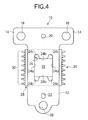
- FIG. 4 is a plan view of the CCD, which is placed on the mounting plate shown in FIG. 1, in such a manner that the front surface of the CCD is attached to the mounting plate;
- FIG. 5 is a plan view of a jig for bonding the CCD at a proper bonding position on the mounting plate;
- FIG. 6 is a front view of the jig, along line VI-VI of FIG. 5;
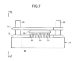
- FIG. 7 is a front view showing a state in which the CCD is sandwiched between the two mounting plates which are attached to the jig;
- FIG. 8 is a side view along line VIII-VIII of FIG. 7;
- FIG. 9 is a plan view showing the state shown in FIG. 7 ;
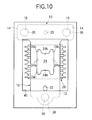
- FIG. 10 is a bottom end view showing the state shown in FIG. 7.
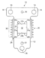
- FIG. 1 shows a plan view of a mounting plate 10 of an embodiment of the present invention.
- the mounting plate 10 has a rectangular portion 12 and a pair of expanded portions 14 which are provided on an end portion of the rectangular portion 12 and project outward in opposite directions.
- the mounting plate 10 has approximately a T-shape as a whole, and can be punched out of a metal plate such as aluminum with a high accuracy.
- a pair of through holes 16 are formed in the expanded portions 14 , and a through hole 18 is formed in another end portion of the rectangular portion 12 .
- These through holes 16 and 18 are arranged in such a manner that the centers of the holes 16 and 18 coincide with the vertexes of an isosceles triangle.
- a small hole 20 is formed halfway between the pair of through holes 16 at one end portion of the rectangular portion 12 , and a slot 22 is formed adjacent to the hole 18 at the other end portion of the rectangular portion 12 .
- the small hole 20 and the slot 22 function as positioning holes when assembling the mounting plate 10 to an inner frame of a digital camera or video camera.
- the positioning holes 20 and 22 are formed with the same accuracy as those of the through holes 16 and 18 .
- two positioning projections which can be fit in the positioning holes 20 and 22 , are provided on portions of the inner frame to which the mounting plate 10 is attached. The assembling operation of the mounting plate 10 is performed while the positioning projections are fit in the positioning holes 20 and 22 , and therefore, the mounting plate 10 is attached at the proper position regardless of the play between the through holes 16 and 18 and the stems of the screws.
- An H-shaped opening 24 is formed in the center portion of the rectangular portion 12 , which functions as an adhesive agent holding portion when a solid-state imaging device such as a CCD is adhered to the mounting plate 10 with an adhesive agent, as described later.
- a periphery of the opening 24 has first, second, and third parts. Namely, the periphery has a pair of first straight edge portions 24 a , a pair of second straight edge portions 24 b perpendicular to the first straight edge portions 24 a , and curved portions 24 c formed at corners between the adjacent straight edge portions 24 a and 24 b .
- the pair of first straight edge portions 24 a are parallel to each other.
- the pair of second straight edge portions 24 b are parallel to each other, and perpendicular to the first straight edge portions 24 a.
- FIG. 2 shows a commercially available CCD 26 , which is the solid-state imaging device to be fixed on the mounting plate 10 .
- the CCD 26 has a package body 28 and a plurality of lead lines 30 extending from opposite side walls of the package body 28 .
- a front surface containing a light receiving area 32 is shown.
- Photodiodes are disposed on the light receiving area 32 and arranged in a matrix. When an image is formed, the image is photo-electrically converted to an electrical image signal through the photodiodes.
- the light receiving area 32 is defined as an effective pixel area of the CCD, and as understood from FIG. 2, the light receiving area 32 is rectangular and formed on the front surface of the package body.
- the CCD 26 is placed on the mounting plate 10 in such a manner that the rear surface of the CCD 26 , which is opposite to the light receiving surface, closes the opening 24 , as shown in FIG. 3.
- An adhesive agent such as a quick-drying adhesive agent or an ultraviolet-curing adhesive agent is then supplied to the periphery of the opening 24 .
- the opening 24 forms an adhesive agent reservoir in association with the rear surface of the CCD 26 . Namely, after the adhesive agent is supplied to the adhesive agent reservoir, and has set, the CCD 26 is completely attached to the mounting plate 10 .
- the attaching operation of the mounting plate 10 to an inner frame of the digital camera or video camera is duly carried out with the engagement of the positioning holes 20 and 22 and the positioning projections. Therefore, for properly positioning the light receiving area 32 of the CCD 26 with respect to the photographing optical system of the digital camera or video camera, the CCD 26 should be bonded to the mounting plate 10 at a proper position.
- the position of-the light receiving area 32 relative to the package body 28 is not necessarily uniform even in products manufactured with the identical standards at the same production facility. Accordingly, the package body 28 cannot be used as the reference for the positioning of the light receiving area 32 relative to the mounting plate 10 . Instead, the light receiving area 32 itself should be used as a reference to the mounting plate 10 . Therefore, in the embodiment, at least two edge portions of the opening 24 of the mounting plate 10 are used for or function as, reference lines for positioning the light receiving area 32 of the CCD 26 over the opening 24 .
- the pair of first edge portions 24 a and the pair of second edge portions 24 b are extended along the contour of the light receiving area 32 of the CCD 26 . Therefore, when the opening 24 is positioned relative to the light receiving area 32 in such a manner that the two pairs of edge portions 24 a and 24 b are aligned on the contour of the light receiving area 32 as shown in FIG. 4, the CCD 26 is positioned at the proper bonding position relative to the mounting plate 10 . However, since the surface of the CCD 26 to be bonded to the mounting plate 10 is opposite to the light receiving surface, an adhesive agent cannot be supplied to the opening 24 of the mounting plate 10 in a state as shown in FIG. 4.
- two mounting plates having the same structure are provided, and the CCD 26 is bonded or fixed to one of the mounting plates 10 .
- one mounting plate is referred to as the mounting plate 10
- the other mounting plate is referred to as the sub-mounting plate 10 ′.
- a bonding method is described below.
- the CCD 26 is sandwiched between the two mounting plates 10 , and the mounting plate 10 and the sub-mounting plate 10 ′ are adjusted to align with each other.
- the light receiving area 32 of the CCD 26 is positioned over the opening 24 of the sub-mounting plate 10 ′ in such a manner that the reference lines or the two pairs of edge portions 24 a and 24 b of the opening 24 of the sub-mounting plate 10 ′, which is placed on the front surface of the CCD 26 , are coincident with the contour of the light receiving area 24 of the sub-mounting plate 10 ′.
- the CCD 26 is positioned at the proper bonding position relative to the sub-mounting plate 10 ′ which is placed on the front surface of the CCD 26 .
- the mounting plate 10 and the sub-mounting plate 10 ′ are aligned with each other, when the CCD 26 is positioned at the proper bonding position relative to the sub-mounting plate 10 ′ placed on the front surface, the CCD 26 is also positioned at the proper bonding position relative to the mounting plate 10 placed on the rear surface of the CCD 26 .
- an adhesive agent is poured in the opening 24 of the mounting plate 10 placed on the rear surface of the CCD 26 .
- the positional relationship between the CCD 26 and the mounting plate 10 attached to the rear surface of the CCD 26 is kept until the adhesive agent has dried.
- the sub-mounting plate 10 ′ is removed from the front surface of the CCD 26 , so that a state, in which the CCD 26 is bonded at the proper bonding position relative to the mounting plate 10 , is obtained.
- the jig has a rectangular body 34 , a pair of guide poles 36 planted close to one side of the rectangular body 34 , and a guide pole 38 planted in the center close to the opposite side of the rectangular body 34 .
- a rectangular opening 40 is formed in the rectangular plate 34 .
- the centers of the three guide poles 36 and 38 coincide with the vertexes of an isosceles triangle, which is identical with the isosceles triangle defined by the centers of the holes 16 and 18 formed in each of the mounting plate 10 and the sub-mounting plate 10 ′.
- the outer diameters of the pair of guide poles 36 substantially coincide with the inner diameters of the pair of through holes 16
- the outer diameter of the guide pole 38 substantially coincides with the inner diameter of the through hole 18 . Namely, the difference between each of the through holes 16 , 18 and each of the guide poles 36 , 38 is very small.
- the CCD 26 is sandwiched between the mounting plate 10 and the sub-mounting plate 10 ′ which are aligned with each other, and under this condition, the front surface of the CCD 26 is placed on the sub-mounting plate 10 ′, and the rear surface of the CCD 26 is placed on the mounting plate 10 .
- the CCD 26 is positioned at the proper bonding position relative to the sub-mounting plate 10 ′ which is located at the upper side as shown in FIG. 9, the CCD 26 is also positioned at the proper bonding position relative to the mounting plate 10 which is located at the lower side as shown in FIG. 10.
- a quick-drying adhesive agent When a quick-drying adhesive agent is used as an adhesive agent, the operator keeps hold of the jig until the agent is dried. Conversely, when an ultraviolet-curing adhesive agent is used, ultraviolet light is irradiated onto the ultraviolet-curing adhesive agent while the operator holds the jig, so that the ultraviolet-curing adhesive agent dries. After the adhesive agent has dried, the upper or sub-mounting plate 10 ′ is removed from the jig, and the lower or mounting plate 10 , to which the CCD 26 is attached, is removed from the jig.
- the mounting plate 10 to which the CCD 26 is attached, is fixed on an inner frame housed in a digital camera or video camera, with a screw, the light receiving area 32 of the CCD 26 is properly positioned with respect to the photographing optical system.
- the shape of the opening of the mounting plate 10 may be coincident with the rectangular contour of the light receiving area 32 of the CCD 26 , and it is preferable that the curved portions 24 c are formed at the corners of the periphery of the opening 24 as described above. This is because, by providing the curved portions 24 c on the periphery of the opening 24 , the amount of periphery of the mounting plate 10 bonded to the CCD 26 is increased. As a result, the bonding of the mounting plate 10 to the CCD 26 is strengthened.
- the curved portions 24 c which are recessed or rounded at the corners, are provided, even if too much adhesive agent is supplied, the excessive adhesive agent flows into the curved portions 24 c and is reserved there, so that excessive adhesive agent is prevented from protruding from the mounting plate 10 and the adhesive agent is uniformly distributed over the two pairs of edge portions 24 a and 24 b . Therefore, uniform and stable bonding occurs along the edge portions 24 a and 24 b.
- the curved portions 24 c are provided at the periphery of the opening 24 so as to increase the bonding periphery of the mounting plate 10 to the CCD 26
- other constructions can be employed.
- relatively small saw-toothed portions can be formed along a part of the periphery of the opening 24 .
- reference lines extending along four edge portions 24 a and 24 b of the light receiving area 32 are provided.
- the positioning of the opening 24 relative to the rectangular light receiving area 32 can be carried out by providing two reference lines extending along two edge portions of the light receiving area 32 , which are perpendicular to each other.
- a simplified attaching operation in which a mounting plate, to which a solid-state imaging device is bonded, is attached to an inner frame of a digital camera or video camera, is performed, so that the manufacturing cost of the digital camera or video camera is drastically reduced.
Abstract
Description
- 1. Field of the Invention
- The present invention relates to a mounting plate to which a solid-state imaging device is attached, and a method for bonding the solid-state imaging device to the mounting plate.
- 2. Description of the Related Art
- As is well known, a solid-state imaging device such as a CCD is used in a digital camera or a video camera. The solid-state imaging device is available as an electronic package, which is not usually directly mounted in the digital camera or video camera. This is because the solid-state imaging device needs to be placed at a proper position relative to a photographing optical system of the digital camera or video camera, and it is difficult to hold the solid-state imaging device at the proper position by itself (i.e., as a single body).
- Therefore, conventionally, the solid-state imaging device is fixed on a mounting plate with an adhesive agent, and the mounting plate is then attached to an inner frame provided inside the digital camera or video camera, with a screw. The digital camera or video camera is usually designed in such a manner that, when the mounting plate to which the solid-state imaging device is bonded, is fixed with a screw, the solid-state imaging device is positioned at a proper position relative to the photographing optical system. Accordingly, the positioning accuracy of the solid-state imaging device with respect to the photographing optical system depends upon how exact the solid-state imaging device is bonded in position on the mounting plate.
- Conventionally, an opening having an appropriate shape, such as a circle, is formed in a mounting plate, and a positioning mark for positioning the solid-state imaging device is formed on a bonding surface to which the solid-state imaging device is bonded. The solid-state imaging device is placed on the bonding surface in such a manner that a rear surface of the solid-state imaging device closes the opening, and the solid-state imaging device package is then positioned according to the positioning mark on the mounting plate. After that, an appropriate adhesive agent is supplied to the opening, and dried so that the solid-state imaging device is fixed on the mounting plate.
- When positioning a solid-state imaging device with respect to the photographing optical system of a digital camera or video camera, the light receiving area of the solid-state imaging device should be positioned in a proper position relative to the photographing optical system. However, the position of the light receiving area relative to a solid-state imaging device package is not uniform, but may be slightly different even in a device manufactured with the identical standards. Therefore, conventionally, even if the solid-state imaging device package is positioned according to the positioning mark, and bonded on the mounting plate, the light receiving area is not necessarily positioned correctly.
- Thus, conventionally, when a mount plate, on which a solid-state imaging device is bonded, is fixed with a screw to an inner frame provided inside a digital camera or video camera, it is necessary to finely adjust the screwed position of the mounting plate within the range of play available between the hole of the mounting plate and the stem of the screw. Due to this, the operation of screwing the mounting plate to the inner frame inside the digital camera or video camera takes time, which makes the assembly cost of the digital camera or video camera expensive.
- Further, in a conventional mounting plate, the shape of the opening is simple, such as circular, and when an adhesive agent is supplied to a simple-shaped opening to bond the solid-state imaging device to the mounting plate, the bonding takes place at the periphery of the circular opening, so that sufficient bonding strength cannot be obtained.
- Therefore, an object of the present invention is to provide a mounting plate in which the shape of the opening for bonding the solid-state imaging device is improved such that the light receiving area of the solid-state imaging device is properly positioned when the solid-state imaging device is bonded on the mounting plate.
- According to the present invention, there is provided a mounting plate having an opening provided for bonding a solid-state imaging device thereto, the solid-state imaging device having a light receiving area. The mounting plate comprises a first edge portion and a second edge portion. The first edge portion defines a first part of the periphery of the opening. The second edge portion defines a second part of the periphery of the opening. The first and second edge portions extend along a contour of the light receiving area to function as reference lines for positioning the solid-state imaging device over the opening.
- The mounting plate may further comprise a third edge portion that defines a third part of the periphery of the opening. The third edge portion is formed in such a manner that a bonding periphery of the mounting plate to the solid-state imaging device is increased. Due to this, the strength of the bonding between the solid-state imaging device and the mounting plate is increased.
- The first and second edge portions may be straight, and the third edge portion may be curved.
- The first edge portion may be perpendicular to the second edge portion.
- Another object of the present invention is to provide a mounting method by which the solid-state imaging device is bonded at a proper position on the mounting plate.
- According to the present invention, there is provided a method for bonding a solid-state imaging device, having a light receiving area, to a mounting plate that comprises a first edge portion and a second edge portion, the first and second edge portions defining a periphery of an opening, the first and second edge portions corresponding to a contour of the light receiving area so as to function as reference lines for positioning the solid-state imaging device over the opening. The method comprises providing a sub-mounting plate having the same structure as that of the mounting plate, sandwiching the solid-state imaging device between the mounting plate and the sub-mounting plate which are aligned with each other, positioning the solid-state imaging device over the opening by adjusting the reference line of the sub-mounting plate to align with the contour of the light receiving area, while keeping the mounting plate and the sub-mounting plate aligned with each other, and supplying adhesive agent to the periphery of the opening of the mounting plate, so that the solid-state imaging device is attached to the mounting plate.
- The objects and advantages of the present invention will be better understood from the following description, with reference to the accompanying drawings in which:
- FIG. 1 is a plan view of a mounting plate of an embodiment of the present invention;
- FIG. 2 is a plan view of a CCD which is to be fixed on the mounting plate;
- FIG. 3 is a plan view of the CCD shown in FIG. 2, which is placed on the mounting plate shown in FIG. 1, in such a manner that the rear surface of the CCD is attached to the mounting plate;
- FIG. 4 is a plan view of the CCD, which is placed on the mounting plate shown in FIG. 1, in such a manner that the front surface of the CCD is attached to the mounting plate;
- FIG. 5 is a plan view of a jig for bonding the CCD at a proper bonding position on the mounting plate;
- FIG. 6 is a front view of the jig, along line VI-VI of FIG. 5;
- FIG. 7 is a front view showing a state in which the CCD is sandwiched between the two mounting plates which are attached to the jig;
- FIG. 8 is a side view along line VIII-VIII of FIG. 7;
- FIG. 9 is a plan view showing the state shown in FIG. 7; and
- FIG. 10 is a bottom end view showing the state shown in FIG. 7.
- The present invention will be described below with reference to the embodiments shown in the drawings.
- FIG. 1 shows a plan view of a
mounting plate 10 of an embodiment of the present invention. Themounting plate 10 has arectangular portion 12 and a pair of expandedportions 14 which are provided on an end portion of therectangular portion 12 and project outward in opposite directions. Namely, themounting plate 10 has approximately a T-shape as a whole, and can be punched out of a metal plate such as aluminum with a high accuracy. - A pair of through
holes 16 are formed in the expandedportions 14, and a throughhole 18 is formed in another end portion of therectangular portion 12. These throughholes holes holes holes mounting plate 10 is attached or fixed to the inner frame. - A
small hole 20 is formed halfway between the pair of throughholes 16 at one end portion of therectangular portion 12, and aslot 22 is formed adjacent to thehole 18 at the other end portion of therectangular portion 12. Thesmall hole 20 and theslot 22 function as positioning holes when assembling themounting plate 10 to an inner frame of a digital camera or video camera. Thepositioning holes holes positioning holes mounting plate 10 is attached. The assembling operation of themounting plate 10 is performed while the positioning projections are fit in thepositioning holes mounting plate 10 is attached at the proper position regardless of the play between the throughholes - An H-
shaped opening 24 is formed in the center portion of therectangular portion 12, which functions as an adhesive agent holding portion when a solid-state imaging device such as a CCD is adhered to themounting plate 10 with an adhesive agent, as described later. - A periphery of the
opening 24 has first, second, and third parts. Namely, the periphery has a pair of firststraight edge portions 24 a, a pair of secondstraight edge portions 24 b perpendicular to the firststraight edge portions 24 a, andcurved portions 24 c formed at corners between the adjacentstraight edge portions straight edge portions 24 a are parallel to each other. The pair of secondstraight edge portions 24 b are parallel to each other, and perpendicular to the firststraight edge portions 24 a. - FIG. 2 shows a commercially
available CCD 26, which is the solid-state imaging device to be fixed on the mountingplate 10. TheCCD 26 has apackage body 28 and a plurality oflead lines 30 extending from opposite side walls of thepackage body 28. In FIG. 2, a front surface containing alight receiving area 32 is shown. Photodiodes are disposed on thelight receiving area 32 and arranged in a matrix. When an image is formed, the image is photo-electrically converted to an electrical image signal through the photodiodes. Note that thelight receiving area 32 is defined as an effective pixel area of the CCD, and as understood from FIG. 2, thelight receiving area 32 is rectangular and formed on the front surface of the package body. - For bonding the CCD onto the mounting
plate 10, first theCCD 26 is placed on the mountingplate 10 in such a manner that the rear surface of theCCD 26, which is opposite to the light receiving surface, closes theopening 24, as shown in FIG. 3. An adhesive agent such as a quick-drying adhesive agent or an ultraviolet-curing adhesive agent is then supplied to the periphery of theopening 24. Thus, the opening 24 forms an adhesive agent reservoir in association with the rear surface of theCCD 26. Namely, after the adhesive agent is supplied to the adhesive agent reservoir, and has set, theCCD 26 is completely attached to the mountingplate 10. - As described above, the attaching operation of the mounting
plate 10 to an inner frame of the digital camera or video camera is duly carried out with the engagement of the positioning holes 20 and 22 and the positioning projections. Therefore, for properly positioning thelight receiving area 32 of theCCD 26 with respect to the photographing optical system of the digital camera or video camera, theCCD 26 should be bonded to the mountingplate 10 at a proper position. - However, the position of-the
light receiving area 32 relative to thepackage body 28 is not necessarily uniform even in products manufactured with the identical standards at the same production facility. Accordingly, thepackage body 28 cannot be used as the reference for the positioning of thelight receiving area 32 relative to the mountingplate 10. Instead, thelight receiving area 32 itself should be used as a reference to the mountingplate 10. Therefore, in the embodiment, at least two edge portions of theopening 24 of the mountingplate 10 are used for or function as, reference lines for positioning thelight receiving area 32 of theCCD 26 over theopening 24. - Namely, as shown in FIG. 4, the pair of
first edge portions 24 a and the pair ofsecond edge portions 24 b are extended along the contour of thelight receiving area 32 of theCCD 26. Therefore, when theopening 24 is positioned relative to thelight receiving area 32 in such a manner that the two pairs ofedge portions light receiving area 32 as shown in FIG. 4, theCCD 26 is positioned at the proper bonding position relative to the mountingplate 10. However, since the surface of theCCD 26 to be bonded to the mountingplate 10 is opposite to the light receiving surface, an adhesive agent cannot be supplied to theopening 24 of the mountingplate 10 in a state as shown in FIG. 4. - Therefore, in the embodiment, two mounting plates having the same structure are provided, and the
CCD 26 is bonded or fixed to one of the mountingplates 10. Hereinafter, one mounting plate is referred to as the mountingplate 10, and the other mounting plate is referred to as thesub-mounting plate 10′. A bonding method is described below. - First, the
CCD 26 is sandwiched between the two mountingplates 10, and the mountingplate 10 and thesub-mounting plate 10′ are adjusted to align with each other. - Then, while keeping the adjusted condition of the mounting
plate 10 and thesub-mounting plate 10′, thelight receiving area 32 of theCCD 26 is positioned over the opening 24 of thesub-mounting plate 10′ in such a manner that the reference lines or the two pairs ofedge portions opening 24 of thesub-mounting plate 10′, which is placed on the front surface of theCCD 26, are coincident with the contour of thelight receiving area 24 of thesub-mounting plate 10′. Thus, theCCD 26 is positioned at the proper bonding position relative to thesub-mounting plate 10′ which is placed on the front surface of theCCD 26. - Since the mounting
plate 10 and thesub-mounting plate 10′ are aligned with each other, when theCCD 26 is positioned at the proper bonding position relative to thesub-mounting plate 10′ placed on the front surface, theCCD 26 is also positioned at the proper bonding position relative to the mountingplate 10 placed on the rear surface of theCCD 26. - Then, an adhesive agent is poured in the
opening 24 of the mountingplate 10 placed on the rear surface of theCCD 26. The positional relationship between theCCD 26 and the mountingplate 10 attached to the rear surface of theCCD 26 is kept until the adhesive agent has dried. After the adhesive agent has dried, thesub-mounting plate 10′ is removed from the front surface of theCCD 26, so that a state, in which theCCD 26 is bonded at the proper bonding position relative to the mountingplate 10, is obtained. - For performing the above described bonding method, the following jig shown in FIGS. 5 and 6 can be utilized. The jig has a
rectangular body 34, a pair ofguide poles 36 planted close to one side of therectangular body 34, and aguide pole 38 planted in the center close to the opposite side of therectangular body 34. Arectangular opening 40 is formed in therectangular plate 34. The centers of the threeguide poles holes plate 10 and thesub-mounting plate 10′. The outer diameters of the pair ofguide poles 36 substantially coincide with the inner diameters of the pair of throughholes 16, and the outer diameter of theguide pole 38 substantially coincides with the inner diameter of the throughhole 18. Namely, the difference between each of the throughholes guide poles - As shown in FIGS. 7 and 8, when the mounting
plate 10 and thesub-mounting plate 10′ are mounted on the jig while the throughholes guide poles plate 10 and thesub-mounting plate 10′ are aligned with each other. Note that, as described above, since the difference between each of the throughholes guide poles plate 10 or thesub-mounting plate 10′ cannot be mounted on the jig as shown in FIGS. 7 and 8, the mountingplate 10 or thesub-mounting plate 10′ is abandoned as a defective article. - The
CCD 26 is sandwiched between the mountingplate 10 and thesub-mounting plate 10′ which are aligned with each other, and under this condition, the front surface of theCCD 26 is placed on thesub-mounting plate 10′, and the rear surface of theCCD 26 is placed on the mountingplate 10. Thus, when theCCD 26 is positioned at the proper bonding position relative to thesub-mounting plate 10′ which is located at the upper side as shown in FIG. 9, theCCD 26 is also positioned at the proper bonding position relative to the mountingplate 10 which is located at the lower side as shown in FIG. 10. - When the positioning of the
CCD 26 over the mountingplate 10 has been completed, therectangular plate 34 of the jig and the upper orsub-mounting plate 10′ are turned over by the operator while maintaining the sandwich condition, so that the bottom side of the jig faces upward. This state is shown in FIG. 9. In this state, an adhesive agent is supplied along the periphery of theopening 24 of the mountingplate 10, placed on the rear surface of theCCD 26, through therectangular opening 40 of therectangular plate 34, and thus, filled between the peripheral wall of theopening 24 and a portion of the rear surface of theCCD 26, close to the peripheral wall. - When a quick-drying adhesive agent is used as an adhesive agent, the operator keeps hold of the jig until the agent is dried. Conversely, when an ultraviolet-curing adhesive agent is used, ultraviolet light is irradiated onto the ultraviolet-curing adhesive agent while the operator holds the jig, so that the ultraviolet-curing adhesive agent dries. After the adhesive agent has dried, the upper or
sub-mounting plate 10′ is removed from the jig, and the lower or mountingplate 10, to which theCCD 26 is attached, is removed from the jig. - When the mounting
plate 10, to which theCCD 26 is attached, is fixed on an inner frame housed in a digital camera or video camera, with a screw, thelight receiving area 32 of theCCD 26 is properly positioned with respect to the photographing optical system. - The shape of the opening of the mounting
plate 10 may be coincident with the rectangular contour of thelight receiving area 32 of theCCD 26, and it is preferable that thecurved portions 24 c are formed at the corners of the periphery of theopening 24 as described above. This is because, by providing thecurved portions 24 c on the periphery of theopening 24, the amount of periphery of the mountingplate 10 bonded to theCCD 26 is increased. As a result, the bonding of the mountingplate 10 to theCCD 26 is strengthened. - Further, since the
curved portions 24 c, which are recessed or rounded at the corners, are provided, even if too much adhesive agent is supplied, the excessive adhesive agent flows into thecurved portions 24 c and is reserved there, so that excessive adhesive agent is prevented from protruding from the mountingplate 10 and the adhesive agent is uniformly distributed over the two pairs ofedge portions edge portions - Although, in the embodiment, the
curved portions 24 c are provided at the periphery of theopening 24 so as to increase the bonding periphery of the mountingplate 10 to theCCD 26, other constructions can be employed. For example, relatively small saw-toothed portions can be formed along a part of the periphery of theopening 24. - In the embodiment, for positioning the
opening 24 relative to the rectangularlight receiving area 32, reference lines extending along fouredge portions light receiving area 32 are provided. Conversely, the positioning of theopening 24 relative to the rectangularlight receiving area 32 can be carried out by providing two reference lines extending along two edge portions of thelight receiving area 32, which are perpendicular to each other. - According to the embodiment, a simplified attaching operation in which a mounting plate, to which a solid-state imaging device is bonded, is attached to an inner frame of a digital camera or video camera, is performed, so that the manufacturing cost of the digital camera or video camera is drastically reduced.
- Although the embodiments of the present invention have been described herein with reference to the accompanying drawings, obviously many modifications and changes may be made by those skilled in this art without departing from the scope of the invention.
- The present disclosure relates to subject matter contained in Japanese Patent Application No. 2002-051096 (filed on Feb. 27, 2002) which is expressly incorporated herein, by reference, in its entirety.
Claims (6)
Applications Claiming Priority (2)
| Application Number | Priority Date | Filing Date | Title |
|---|---|---|---|
| JP2002051096A JP4477811B2 (en) | 2002-02-27 | 2002-02-27 | Mounting plate for solid-state image sensor and mounting method to the mounting plate |
| JPP2002-051096 | 2002-02-27 |
Publications (2)
| Publication Number | Publication Date |
|---|---|
| US20030197786A1 true US20030197786A1 (en) | 2003-10-23 |
| US7436443B2 US7436443B2 (en) | 2008-10-14 |
Family
ID=19192872
Family Applications (1)
| Application Number | Title | Priority Date | Filing Date |
|---|---|---|---|
| US10/373,070 Expired - Fee Related US7436443B2 (en) | 2002-02-27 | 2003-02-26 | Mounting plate for solid-state imaging device and method for bonding solid-state imaging device to mounting plate |
Country Status (8)
| Country | Link |
|---|---|
| US (1) | US7436443B2 (en) |
| JP (1) | JP4477811B2 (en) |
| KR (1) | KR100963851B1 (en) |
| CN (1) | CN100507699C (en) |
| DE (1) | DE10308524A1 (en) |
| FR (1) | FR2836598B1 (en) |
| GB (1) | GB2387483B (en) |
| TW (1) | TWI290446B (en) |
Cited By (4)
| Publication number | Priority date | Publication date | Assignee | Title |
|---|---|---|---|---|
| US20050024529A1 (en) * | 2003-07-29 | 2005-02-03 | Pentax Corporation | Digital camera |
| US20050025475A1 (en) * | 2003-07-29 | 2005-02-03 | Pentax Corporation | Camera body |
| US20060001755A1 (en) * | 2004-06-30 | 2006-01-05 | Pentax Corporation | Solid state imaging device |
| US20120066887A1 (en) * | 2010-09-22 | 2012-03-22 | Itt Manufacturing Enterprises, Inc. | Method of aligning an imaging device in an optical system |
Families Citing this family (20)
| Publication number | Priority date | Publication date | Assignee | Title |
|---|---|---|---|---|
| CN100427357C (en) * | 2005-11-01 | 2008-10-22 | 江南造船(集团)有限责任公司 | Multifunctional equipment of tool set up in use for installing towed bird type electric propulsion plant |
| SE533704C2 (en) | 2008-12-05 | 2010-12-07 | Flatfrog Lab Ab | Touch sensitive apparatus and method for operating the same |
| JP4560121B2 (en) * | 2008-12-17 | 2010-10-13 | 株式会社東芝 | Sensor fixing device and camera module |
| JP5864890B2 (en) * | 2011-04-26 | 2016-02-17 | キヤノン株式会社 | Imaging device |
| CN104349079B (en) * | 2013-07-29 | 2018-07-24 | 光宝科技股份有限公司 | Image sensing module |
| JP6157993B2 (en) * | 2013-08-27 | 2017-07-05 | 東芝メディカルシステムズ株式会社 | Image sensor fixing method and image sensor positioning jig |
| EP3250993B1 (en) | 2015-01-28 | 2019-09-04 | FlatFrog Laboratories AB | Dynamic touch quarantine frames |
| US10496227B2 (en) | 2015-02-09 | 2019-12-03 | Flatfrog Laboratories Ab | Optical touch system comprising means for projecting and detecting light beams above and inside a transmissive panel |
| JP2018536944A (en) | 2015-12-09 | 2018-12-13 | フラットフロッグ ラボラトリーズ アーベーFlatFrog Laboratories AB | Improved stylus identification |
| CN209046978U (en) * | 2016-02-12 | 2019-06-28 | 平蛙实验室股份公司 | Assembling tool and set group for panel and touch sensing system |
| US10761657B2 (en) | 2016-11-24 | 2020-09-01 | Flatfrog Laboratories Ab | Automatic optimisation of touch signal |
| KR20240012622A (en) | 2016-12-07 | 2024-01-29 | 플라트프로그 라보라토리즈 에이비 | An improved touch device |
| CN116679845A (en) | 2017-02-06 | 2023-09-01 | 平蛙实验室股份公司 | Touch sensing device |
| US10606414B2 (en) | 2017-03-22 | 2020-03-31 | Flatfrog Laboratories Ab | Eraser for touch displays |
| EP4036697A1 (en) | 2017-03-28 | 2022-08-03 | FlatFrog Laboratories AB | Optical touch sensing apparatus |
| CN117311543A (en) | 2017-09-01 | 2023-12-29 | 平蛙实验室股份公司 | Touch sensing device |
| WO2019172826A1 (en) | 2018-03-05 | 2019-09-12 | Flatfrog Laboratories Ab | Improved touch-sensing apparatus |
| US11943563B2 (en) | 2019-01-25 | 2024-03-26 | FlatFrog Laboratories, AB | Videoconferencing terminal and method of operating the same |
| EP4104042A1 (en) | 2020-02-10 | 2022-12-21 | FlatFrog Laboratories AB | Improved touch-sensing apparatus |
| JP2022060038A (en) * | 2020-10-02 | 2022-04-14 | 住友電気工業株式会社 | Method of manufacturing optical module and optical module |
Citations (19)
| Publication number | Priority date | Publication date | Assignee | Title |
|---|---|---|---|---|
| US4594613A (en) * | 1982-02-16 | 1986-06-10 | Canon Kabushiki Kaisha | Solid-state imaging device assembly |
| US5172236A (en) * | 1989-08-23 | 1992-12-15 | Ricoh Company, Ltd. | Electronic pan-focusing apparatus for producing focused images independent of depth of field and type of lens |
| US5307170A (en) * | 1990-10-29 | 1994-04-26 | Kabushiki Kaisha Toshiba | Video camera having a vibrating image-processing operation |
| US5614763A (en) * | 1995-03-13 | 1997-03-25 | Zetetic Institute | Methods for improving performance and temperature robustness of optical coupling between solid state light sensors and optical systems |
| US5731834A (en) * | 1995-06-07 | 1998-03-24 | Eastman Kodak Company | Replaceable CCD array and method of assembly |
| US5739853A (en) * | 1994-01-13 | 1998-04-14 | Matsushita Electric Industrial Co., Ltd. | Device for supporting optical system of television camera and having two spring systems for reducing rattling in two different directions |
| US5861654A (en) * | 1995-11-28 | 1999-01-19 | Eastman Kodak Company | Image sensor assembly |
| US5870638A (en) * | 1996-09-03 | 1999-02-09 | Asahi Kogaku Kogyo Kabushiki Kaisha | Camera having two operative modes |
| US5883386A (en) * | 1996-09-17 | 1999-03-16 | Seiko Precision Inc. | Light-receiving apparatus having a position detectable portion on a sealing frame and its manufacturing method |
| US5952714A (en) * | 1995-08-02 | 1999-09-14 | Matsushita Electronics Corporation | Solid-state image sensing apparatus and manufacturing method thereof |
| US6035147A (en) * | 1996-09-03 | 2000-03-07 | Asahi Kogaku Kogyo Kabushiki Kaisha | CCD mounting structure for exchangeable camera back |
| US6040612A (en) * | 1997-02-07 | 2000-03-21 | Fuji Photo Optical Co., Ltd. | Image pickup apparatus for endoscope having reduced diameter |
| US6240253B1 (en) * | 1998-09-14 | 2001-05-29 | Minolta Co., Ltd. | Automatic focusing camera |
| US20010010562A1 (en) * | 2000-01-28 | 2001-08-02 | Asahi Kogaku Kogyo Kabushiki Kaisha | Structure for mounting a solid-state imaging device |
| US6433328B1 (en) * | 2000-08-07 | 2002-08-13 | Umax Data Systems, Inc. | Stray light attenuating device |
| US6646316B2 (en) * | 2001-01-24 | 2003-11-11 | Kingpak Technology, Inc. | Package structure of an image sensor and packaging |
| US6654064B2 (en) * | 1997-05-23 | 2003-11-25 | Canon Kabushiki Kaisha | Image pickup device incorporating a position defining member |
| US6784409B2 (en) * | 2000-03-28 | 2004-08-31 | Canon Kabushiki Kaisha | Electronic device with encapsulant of photo-set resin and production process of same |
| US6956610B1 (en) * | 1999-02-18 | 2005-10-18 | Linvatec Corporation | Shock mounting system for CCD camera |
Family Cites Families (4)
| Publication number | Priority date | Publication date | Assignee | Title |
|---|---|---|---|---|
| JPS59226568A (en) * | 1983-06-08 | 1984-12-19 | Toshiba Corp | Solid state image pickup device |
| JPH1023340A (en) * | 1996-07-05 | 1998-01-23 | Matsushita Electric Works Ltd | Solid-state image pickup device |
| JP4169938B2 (en) * | 2000-01-28 | 2008-10-22 | Hoya株式会社 | Solid-state image sensor holding block and solid-state image sensor mounting structure |
| JP4185236B2 (en) * | 2000-06-19 | 2008-11-26 | イーストマン コダック カンパニー | Solid-state imaging device and imaging apparatus |
-
2002
- 2002-02-27 JP JP2002051096A patent/JP4477811B2/en not_active Expired - Fee Related
-
2003
- 2003-02-26 TW TW092104101A patent/TWI290446B/en active
- 2003-02-26 CN CNB031052835A patent/CN100507699C/en not_active Expired - Fee Related
- 2003-02-26 US US10/373,070 patent/US7436443B2/en not_active Expired - Fee Related
- 2003-02-26 KR KR1020030011878A patent/KR100963851B1/en not_active IP Right Cessation
- 2003-02-27 GB GB0304536A patent/GB2387483B/en not_active Expired - Fee Related
- 2003-02-27 FR FR0302406A patent/FR2836598B1/en not_active Expired - Fee Related
- 2003-02-27 DE DE10308524A patent/DE10308524A1/en not_active Withdrawn
Patent Citations (20)
| Publication number | Priority date | Publication date | Assignee | Title |
|---|---|---|---|---|
| US4594613A (en) * | 1982-02-16 | 1986-06-10 | Canon Kabushiki Kaisha | Solid-state imaging device assembly |
| US5172236A (en) * | 1989-08-23 | 1992-12-15 | Ricoh Company, Ltd. | Electronic pan-focusing apparatus for producing focused images independent of depth of field and type of lens |
| US5307170A (en) * | 1990-10-29 | 1994-04-26 | Kabushiki Kaisha Toshiba | Video camera having a vibrating image-processing operation |
| US5739853A (en) * | 1994-01-13 | 1998-04-14 | Matsushita Electric Industrial Co., Ltd. | Device for supporting optical system of television camera and having two spring systems for reducing rattling in two different directions |
| US5614763A (en) * | 1995-03-13 | 1997-03-25 | Zetetic Institute | Methods for improving performance and temperature robustness of optical coupling between solid state light sensors and optical systems |
| US5731834A (en) * | 1995-06-07 | 1998-03-24 | Eastman Kodak Company | Replaceable CCD array and method of assembly |
| US5952714A (en) * | 1995-08-02 | 1999-09-14 | Matsushita Electronics Corporation | Solid-state image sensing apparatus and manufacturing method thereof |
| US5861654A (en) * | 1995-11-28 | 1999-01-19 | Eastman Kodak Company | Image sensor assembly |
| US6035147A (en) * | 1996-09-03 | 2000-03-07 | Asahi Kogaku Kogyo Kabushiki Kaisha | CCD mounting structure for exchangeable camera back |
| US5870638A (en) * | 1996-09-03 | 1999-02-09 | Asahi Kogaku Kogyo Kabushiki Kaisha | Camera having two operative modes |
| US5883386A (en) * | 1996-09-17 | 1999-03-16 | Seiko Precision Inc. | Light-receiving apparatus having a position detectable portion on a sealing frame and its manufacturing method |
| US6040612A (en) * | 1997-02-07 | 2000-03-21 | Fuji Photo Optical Co., Ltd. | Image pickup apparatus for endoscope having reduced diameter |
| US6654064B2 (en) * | 1997-05-23 | 2003-11-25 | Canon Kabushiki Kaisha | Image pickup device incorporating a position defining member |
| US6240253B1 (en) * | 1998-09-14 | 2001-05-29 | Minolta Co., Ltd. | Automatic focusing camera |
| US6956610B1 (en) * | 1999-02-18 | 2005-10-18 | Linvatec Corporation | Shock mounting system for CCD camera |
| US20010010562A1 (en) * | 2000-01-28 | 2001-08-02 | Asahi Kogaku Kogyo Kabushiki Kaisha | Structure for mounting a solid-state imaging device |
| US6956615B2 (en) * | 2000-01-28 | 2005-10-18 | Pentax Corporation | Structure for mounting a solid-state imaging device |
| US6784409B2 (en) * | 2000-03-28 | 2004-08-31 | Canon Kabushiki Kaisha | Electronic device with encapsulant of photo-set resin and production process of same |
| US6433328B1 (en) * | 2000-08-07 | 2002-08-13 | Umax Data Systems, Inc. | Stray light attenuating device |
| US6646316B2 (en) * | 2001-01-24 | 2003-11-11 | Kingpak Technology, Inc. | Package structure of an image sensor and packaging |
Cited By (7)
| Publication number | Priority date | Publication date | Assignee | Title |
|---|---|---|---|---|
| US20050024529A1 (en) * | 2003-07-29 | 2005-02-03 | Pentax Corporation | Digital camera |
| US20050025475A1 (en) * | 2003-07-29 | 2005-02-03 | Pentax Corporation | Camera body |
| US7140788B2 (en) | 2003-07-29 | 2006-11-28 | Pentax Corporation | Camera body |
| US7663694B2 (en) | 2003-07-29 | 2010-02-16 | Hoya Corporation | Digital camera |
| US20060001755A1 (en) * | 2004-06-30 | 2006-01-05 | Pentax Corporation | Solid state imaging device |
| US20120066887A1 (en) * | 2010-09-22 | 2012-03-22 | Itt Manufacturing Enterprises, Inc. | Method of aligning an imaging device in an optical system |
| US8313608B2 (en) * | 2010-09-22 | 2012-11-20 | Exelis, Inc. | Method of aligning an imaging device in an optical system |
Also Published As
| Publication number | Publication date |
|---|---|
| TWI290446B (en) | 2007-11-21 |
| CN100507699C (en) | 2009-07-01 |
| GB2387483A (en) | 2003-10-15 |
| FR2836598A1 (en) | 2003-08-29 |
| KR100963851B1 (en) | 2010-06-16 |
| CN1441309A (en) | 2003-09-10 |
| TW200405778A (en) | 2004-04-01 |
| FR2836598B1 (en) | 2007-06-15 |
| JP2003258214A (en) | 2003-09-12 |
| DE10308524A1 (en) | 2003-09-04 |
| KR20030071518A (en) | 2003-09-03 |
| GB0304536D0 (en) | 2003-04-02 |
| JP4477811B2 (en) | 2010-06-09 |
| US7436443B2 (en) | 2008-10-14 |
| GB2387483B (en) | 2005-09-28 |
Similar Documents
| Publication | Publication Date | Title |
|---|---|---|
| US7436443B2 (en) | Mounting plate for solid-state imaging device and method for bonding solid-state imaging device to mounting plate | |
| JP7071926B2 (en) | Camera module and its photosensitive parts and their manufacturing method | |
| US6011661A (en) | Optical holder for an optical apparatus | |
| US7166907B2 (en) | Image sensor module with substrate and frame and method of making the same | |
| US7391457B2 (en) | Image sensor module with light-shielding diaphragm made of ink, and method of making the same | |
| US6956615B2 (en) | Structure for mounting a solid-state imaging device | |
| EP1246456B1 (en) | Imaging device and manufacturing method thereof | |
| US8164841B2 (en) | Camera module | |
| EP1708278A2 (en) | Optical device module, lens holding device, and method for manufacturing optical device module | |
| US20060093352A1 (en) | Digital still camera module | |
| US20050242410A1 (en) | Camera module, holder for use in a camera module, camera system and method of manufacturing a camera module | |
| US7527441B2 (en) | Camera module, holder for use in a camera module, camera system and method of manufacturing a camera module | |
| JP2000241696A (en) | Holding/mounting method for optical sensor package | |
| US20060110097A1 (en) | Optical device and optical apparatus | |
| US5801374A (en) | Precision optical sensor packaging | |
| US20010052640A1 (en) | Solid image pickup device | |
| JP2001333322A (en) | Solid-state image pickup device, cover, board and lens unit | |
| JPS60212070A (en) | Solid-state image pickup device | |
| JP2006126800A (en) | Camera module | |
| JP2002009264A (en) | Solid state image pickup element and image pickup device | |
| WO1999011056A1 (en) | Ccd mount for mounting a ccd sensor to a camera | |
| JPS5910237A (en) | Semiconductor device and manufacture thereof | |
| EP1150475A2 (en) | Holder and portable telephone with the holder | |
| JPH0574269B2 (en) | ||
| JP2006081007A (en) | Solid-state imaging unit |
Legal Events
| Date | Code | Title | Description |
|---|---|---|---|
| AS | Assignment |
Owner name: PENTAX CORPORATION, JAPAN Free format text: RE-RECORD TO CORRECT THE SERIAL NUMBER PREVIOUSLY RECORDED AT REEL/FRAME 014191/0010;ASSIGNORS:HIRUNUMA, KEN;HOTTA, KEIICHI;FUNATSU, GOUJI;REEL/FRAME:014929/0927 Effective date: 20030402 |
|
| AS | Assignment |
Owner name: HOYA CORPORATION, JAPAN Free format text: MERGER;ASSIGNOR:PENTAX CORPORATION;REEL/FRAME:021320/0337 Effective date: 20080331 |
|
| FEPP | Fee payment procedure |
Free format text: PAYOR NUMBER ASSIGNED (ORIGINAL EVENT CODE: ASPN); ENTITY STATUS OF PATENT OWNER: LARGE ENTITY |
|
| AS | Assignment |
Owner name: PENTAX RICOH IMAGING COMPANY, LTD., JAPAN Free format text: CORPORATE SPLIT;ASSIGNOR:HOYA CORPORATION;REEL/FRAME:027315/0115 Effective date: 20111003 |
|
| FPAY | Fee payment |
Year of fee payment: 4 |
|
| REMI | Maintenance fee reminder mailed | ||
| LAPS | Lapse for failure to pay maintenance fees | ||
| STCH | Information on status: patent discontinuation |
Free format text: PATENT EXPIRED DUE TO NONPAYMENT OF MAINTENANCE FEES UNDER 37 CFR 1.362 |
|
| FP | Lapsed due to failure to pay maintenance fee |
Effective date: 20161014 |