US20030198038A1 - Backlight assembly and liquid crystal display apparatus having the same - Google Patents
Backlight assembly and liquid crystal display apparatus having the same Download PDFInfo
- Publication number
- US20030198038A1 US20030198038A1 US10/295,384 US29538402A US2003198038A1 US 20030198038 A1 US20030198038 A1 US 20030198038A1 US 29538402 A US29538402 A US 29538402A US 2003198038 A1 US2003198038 A1 US 2003198038A1
- Authority
- US
- United States
- Prior art keywords
- electrode
- end portion
- lamp
- lamp tube
- disposed
- Prior art date
- Legal status (The legal status is an assumption and is not a legal conclusion. Google has not performed a legal analysis and makes no representation as to the accuracy of the status listed.)
- Granted
Links
Images


Classifications
-
- G—PHYSICS
- G02—OPTICS
- G02F—OPTICAL DEVICES OR ARRANGEMENTS FOR THE CONTROL OF LIGHT BY MODIFICATION OF THE OPTICAL PROPERTIES OF THE MEDIA OF THE ELEMENTS INVOLVED THEREIN; NON-LINEAR OPTICS; FREQUENCY-CHANGING OF LIGHT; OPTICAL LOGIC ELEMENTS; OPTICAL ANALOGUE/DIGITAL CONVERTERS
- G02F1/00—Devices or arrangements for the control of the intensity, colour, phase, polarisation or direction of light arriving from an independent light source, e.g. switching, gating or modulating; Non-linear optics
- G02F1/01—Devices or arrangements for the control of the intensity, colour, phase, polarisation or direction of light arriving from an independent light source, e.g. switching, gating or modulating; Non-linear optics for the control of the intensity, phase, polarisation or colour
- G02F1/13—Devices or arrangements for the control of the intensity, colour, phase, polarisation or direction of light arriving from an independent light source, e.g. switching, gating or modulating; Non-linear optics for the control of the intensity, phase, polarisation or colour based on liquid crystals, e.g. single liquid crystal display cells
- G02F1/133—Constructional arrangements; Operation of liquid crystal cells; Circuit arrangements
- G02F1/1333—Constructional arrangements; Manufacturing methods
- G02F1/1335—Structural association of cells with optical devices, e.g. polarisers or reflectors
-
- G—PHYSICS
- G02—OPTICS
- G02B—OPTICAL ELEMENTS, SYSTEMS OR APPARATUS
- G02B6/00—Light guides; Structural details of arrangements comprising light guides and other optical elements, e.g. couplings
- G02B6/0001—Light guides; Structural details of arrangements comprising light guides and other optical elements, e.g. couplings specially adapted for lighting devices or systems
- G02B6/0011—Light guides; Structural details of arrangements comprising light guides and other optical elements, e.g. couplings specially adapted for lighting devices or systems the light guides being planar or of plate-like form
- G02B6/0081—Mechanical or electrical aspects of the light guide and light source in the lighting device peculiar to the adaptation to planar light guides, e.g. concerning packaging
- G02B6/0086—Positioning aspects
- G02B6/009—Positioning aspects of the light source in the package
-
- G—PHYSICS
- G02—OPTICS
- G02B—OPTICAL ELEMENTS, SYSTEMS OR APPARATUS
- G02B6/00—Light guides; Structural details of arrangements comprising light guides and other optical elements, e.g. couplings
- G02B6/0001—Light guides; Structural details of arrangements comprising light guides and other optical elements, e.g. couplings specially adapted for lighting devices or systems
- G02B6/0011—Light guides; Structural details of arrangements comprising light guides and other optical elements, e.g. couplings specially adapted for lighting devices or systems the light guides being planar or of plate-like form
- G02B6/0066—Light guides; Structural details of arrangements comprising light guides and other optical elements, e.g. couplings specially adapted for lighting devices or systems the light guides being planar or of plate-like form characterised by the light source being coupled to the light guide
- G02B6/007—Incandescent lamp or gas discharge lamp
- G02B6/0071—Incandescent lamp or gas discharge lamp with elongated shape, e.g. tube
-
- G—PHYSICS
- G02—OPTICS
- G02B—OPTICAL ELEMENTS, SYSTEMS OR APPARATUS
- G02B6/00—Light guides; Structural details of arrangements comprising light guides and other optical elements, e.g. couplings
- G02B6/0001—Light guides; Structural details of arrangements comprising light guides and other optical elements, e.g. couplings specially adapted for lighting devices or systems
- G02B6/0011—Light guides; Structural details of arrangements comprising light guides and other optical elements, e.g. couplings specially adapted for lighting devices or systems the light guides being planar or of plate-like form
- G02B6/0081—Mechanical or electrical aspects of the light guide and light source in the lighting device peculiar to the adaptation to planar light guides, e.g. concerning packaging
- G02B6/0083—Details of electrical connections of light sources to drivers, circuit boards, or the like
Definitions
- the present invention relates to a backlight assembly and an LCD (Liquid Crystal Display) apparatus, and more particularly to a backlight assembly having a reduced size and an LCD apparatus having the same.
- LCD Liquid Crystal Display
- an LCD apparatus can be defined as a display apparatus that allows a user to recognize data processed in an information-processing unit as an image.
- the LCD apparatus uses a liquid crystal in which a light transmittance varies with an intensity of an applied electric field.
- the LCD apparatus requires technologies capable of applying an electric field to a liquid crystal layer and supplying a light having a uniform brightness to the liquid crystal layer.
- the liquid crystal layer may be divided into a number of minute areas each having a different intensity of electrical field applied thereto.
- the technology for applying the electric field to the liquid crystal layer may be performed using a thin film transistor and a transparent conductive thin film.
- the technology for supplying the light to the liquid crystal layer may be performed using a CCFL (Cold Cathode Fluorescent Lamp).
- CCFL Cold Cathode Fluorescent Lamp
- an electron activates a fluorescent material by discharging secondary electrons caused by dissociating ions and photoelectrons caused by recombining the ions to generate the light.
- FIG. 1 is a perspective view showing a conventional CCFL lamp.
- a CCFL 10 includes a lamp tube 5 , a first electrode 8 and a second electrode 9 .
- the lamp tube 5 includes a tube body 4 , a fluorescent material layer 3 disposed on an inner wall of the tube body 4 and a discharge gas 2 injected into the tube body 4 .
- First and second electrodes 8 and 9 are disposed in the tube body, facing each other.
- the CCFL 10 receives a discharge voltage from an external source, which is sufficient to allow electrons to travel from the first electrode 8 to the second electrode 9 and thus generate a visual ray.
- the first and second electrode 8 and 9 are connected to a first lamp wire 8 a and a second lamp wire 9 a using a welding process, respectively.
- the first and second lamp wires 8 a and 9 a are coupled to a lamp wire connector 7 .
- the LCD apparatus needs a CCFL having a length longer than that of the CCFL 10 shown in FIG. 1.
- FIG. 2 is a perspective view showing another conventional lamp.
- reference numerals “21” and “22” indicate first and second lamp tubes, respectively.
- the first and second lamp tubes are L-shaped and paired to form lamp 20 .
- Reference numerals “21a”, “21b”, “ 22 a” and “22b” indicate first to fourth lamp wires for supplying a power voltage to the first and second lamp tubes 21 and 22
- reference numerals “21c” and “21d” indicate lamp wire connectors for the first to fourth lamp wires 21 a , 21 b , 22 a and 22 b.
- the CCFLs 10 and 20 shown in FIGS. 1 and 2 have a lot of disadvantages regarding the size of a corresponding LCD apparatus. Particularly, since the L-shaped CCFL 20 employs the first to fourth lamp wires 21 a , 21 b , 22 a and 22 b having a longer length than that of the CCFL 10 shown in FIG. 1, an entire size of the LCD apparatus that employs the L-shaped CCFL 20 is largely increased.
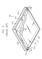
- FIG. 3 is a partially cut perspective view showing an LCD apparatus having an L-shaped lamp.
- the LCD apparatus 30 includes a receiving container 31 for receiving the L-shaped CCFL 20 and a light guide plate 32 for receiving the light from the L-shaped CCFL 20 .
- the receiving container 31 has a hexahedron shape that an upper surface is opened, so that the receiving container 31 has first side surface 31 a , second side surface 31 b , third side surface (not shown), fourth side surface (not shown), and a bottom surface 31 c .
- the light guide plate 32 having a plate shape consisting of four side surfaces, an upper surface and a lower surface is disposed on the bottom surface 31 c of the receiving container 31 .
- the first lamp tube 21 of the L-shaped CCFL 20 having the first and second lamp wires 21 a and 21 b is disposed between the second surface 31 d of the receiving container 31 and the light guide plate 32 .
- the second lamp tube 22 of the L-shape CCFL 20 having the third and fourth lamp wires 22 a and 22 b is disposed between the first surface 31 a of the receiving container 31 and the light guide plate 32 .
- the receiving container 31 further includes a first barrier rib 31 b and a second barrier rib 31 e .
- the first barrier rib 31 b is disposed between the second lamp tube 22 and the first side surface 31 a of the receiving container 31 to provide a first receiving space for the third lamp wire 22 a .
- the second barrier rib 31 e is disposed between the first lamp tube 21 and the second side surface 31 d of the receiving container 31 to provide a second receiving space for the first lamp wire 21 a .
- the third lamp wire 22 a connected to the second lamp tube 22 is received between the first side surface 31 a and the first barrier rib 31 b and the first lamp wire 21 a connected to the first lamp tube 20 is received between the second side surface 31 d and the second barrier rib 31 e.
- the LCD apparatus needs to form the first and second barrier ribs 31 b and 31 e on the receiving container 31 to fix the first and third lamp wires 21 a and 22 a to the receiving container 31 .
- the size of the receiving container 31 increases by sizes of the first and second receiving spaces, thereby increasing the entire size of the LCD apparatus 30 .
- the invention provides a backlight assembly having an entirely reduced size.
- the invention also provides an LCD apparatus having an entirely reduced size.
- a backlight assembly comprising: a light guide plate having a plurality of side surfaces, for changing a direction and an optical property of a light provided from an external source; a first lamp having a first lamp tube disposed adjacent to two of the side surfaces, a first electrode disposed at a first end portion of the first lamp tube and a second electrode disposed at a second end portion opposite the first end portion of the first lamp tube; a second lamp having a second lamp tube disposed adjacent to a remaining two of the side surfaces, a third electrode disposed at a third end portion of the second lamp tube and a fourth electrode disposed at a fourth end portion, the third and fourth end portions being disposed adjacent to the first and second end portions, respectively; connecting means for electrically connecting the first electrode to the third electrode; and power supply means for supplying a first discharge voltage and a second discharge voltage to the second and fourth electrodes, respectively, the first and second discharge voltages having a phase difference of 180° from each other and a same voltage
- a backlight assembly comprising: a light guide plate having four surfaces of a plate shape, for changing a direction and an optical property of a light provided from an external source; a first lamp having a first lamp tube disposed adjacent to two of the four surfaces, a first electrode disposed on a surface of a first end portion of the first lamp tube and a second electrode disposed at an inside of a second end portion opposite the first end portion of the first lamp tube, the first lamp tube having an L shape; a second lamp having a second lamp tube disposed adjacent to a remaining two of the four surfaces, a third electrode disposed on a surface of a third end portion of the second lamp tube and a fourth electrode disposed at an inside of a fourth end portion of the second lamp tube, the third and fourth end portions being disposed adjacent to the first and second end portions, respectively and the second lamp tube having the L shape; a conductive lamp connecting member for electrically connecting the first electrode to the third electrode; and power supply means for supplying a first discharge voltage
- an LCD apparatus comprising: a backlight assembly having a light guide plate having a plurality of side surfaces, for changing a direction and an optical property of a light provided from an external source; a first lamp having a first lamp tube disposed adjacent to two of the side surfaces, a first electrode disposed at a first end portion of the first lamp tube and a second electrode disposed at a second end portion opposite the first end portion of the first lamp tube; a second lamp having a second lamp tube disposed adjacent to a remaining two of the side surfaces, a third electrode disposed at a third end portion of the second lamp tube and a fourth electrode disposed at a fourth end portion, the third and fourth end portions being disposed adjacent to the first and second end portions, respectively; connecting means for electrically connecting the first electrode to the third electrode; and power supply means for supplying a first discharge voltage and a second discharge voltage to the second and fourth electrodes, respectively, the first and second discharge voltages having a phase difference of 180° from each other and a
- the LCD apparatus it is able to remove a lamp wire for supplying a power voltage to the lamp, so that an entire size of the LCD apparatus can be reduced and the lamp can be easily replaced.
- FIG. 1 is a perspective view showing a conventional CCFL
- FIG. 2 is a perspective view showing another conventional CCFL
- FIG. 3 is a partially cut perspective view showing an LCD apparatus having an L-shaped CCFL
- FIG. 4 is a schematic view showing a backlight assembly according to a first embodiment of the present invention.
- FIG. 5 is a cross-sectional view taken along the line C-C showing a structure of a lamp shown in FIG. 4;
- FIG. 6 is a schematic view showing a backlight assembly according to a second embodiment of the present invention.
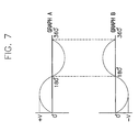
- FIG. 7 is a graph illustrating a phase difference between first and second lamps according to the first embodiment of the present invention.
- FIG. 8 is a perspective view showing a lamp connecting member according to the first embodiment of the present.
- FIG. 9 is a perspective view showing a lamp connecting member according to the second embodiment of the present.
- FIG. 10 is an enlarged view showing a first electrode of the first lamp according to the first embodiment of the present invention.
- FIG. 11 is an enlarged view showing a third electrode of the second lamp according to the first embodiment of the present invention.
- FIG. 12 is an exploded perspective view showing a structure of the lamp connecting member and the first and second lamps according to the first embodiment of the present invention
- FIG. 13 is an exploded perspective view showing an LCD apparatus according to the present invention.
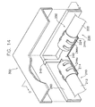
- FIG. 14 is a partially cut perspective view showing the backlight assembly, the lamp connecting member and a chassis according to the present invention.
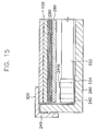
- FIG. 15 is a cross-sectional view taken along the line D-D showing a structure of the LCD apparatus shown in FIG. 13.
- FIG. 4 is a schematic view showing a backlight assembly according to a first embodiment of the present invention.
- a backlight assembly 250 includes a light guide plate 280 , a first lamp 210 , a second lamp 220 , a discharge voltage supply part 230 , a lamp connecting member 240 and a receiving container 260 .
- the light guide plate 280 has a plate shape, that is at least three side surfaces, a light reflecting surface and a light emitting surface.
- the light guide plate 280 has a first, a second, a third and a fourth side surface 281 , 282 , 283 and 284 , respectively,
- the light guide plate 280 changes a direction and an optical property of a light.
- the direction and optical property of the light supplied to the light guide plate 280 through the first to fourth side surfaces 281 , 282 , 283 and 284 are changed during reflecting by the light reflecting surface and emitted through the light emitting surface.
- the first and second lamps 210 and 220 supply the light to the first to fourth side surfaces 281 , 282 , 283 and 284 of the light guide plate 280 .
- the first lamp 210 supplies the light to the first and second side surfaces 281 and 282 , respectively, of the light guide plate 280 and the second lamp 220 supplies the light to the third and fourth side surfaces 283 and 284 , respectively,
- the first lamp 210 has an L shape bent to an angle identical to that between the first side surface 281 and the second side surface 282 .
- the second lamp 220 has an L shape bent to an angle identical to that between the third side surface 283 and the fourth side surface 284 .
- the first and second lamps 210 and 220 have two end portions.
- the first lamp 210 has a first end portion 212 d and a second end portion 212 e and the second lamp 220 has a third end portion 222 d and a fourth end portion 222 e.
- the first end portion 212 d of the first lamp 210 and the third end portion 222 d of the second lamp 220 are disposed adjacent to a corner formed by the second and third side surfaces 282 and 283 , respectively.
- the second end portion 212 e of the first lamp 210 and the fourth end portion 222 e of the second lamp 220 are disposed adjacent to a corner formed by the first and fourth side surfaces 281 and 284 , respectively.
- FIG. 5 is a cross-sectional view taken along the line C-C showing a structure of a lamp shown in FIG. 4.
- FIG. 7 is a graph illustrating a phase difference between first and second lamps according to the first embodiment of the present invention.
- the first lamp 210 includes a first lamp tube 212 having an L shape, a first electrode 214 and a second electrode 216 .
- the first lamp tube 212 includes a first lamp tube body 212 a , a fluorescent material 212 b disposed on an inner wall of the first lamp tube body 212 a and a discharge gas 212 c .
- the first lamp tube 212 further includes a first electrode 214 and a second electrode 216 disposed at the first and second end portions 212 d and 212 e , respectively.
- the first and second electrodes 214 and 216 receive a discharge voltage.
- the second lamp 220 includes a second lamp tube 222 having the L shape, a third electrode 224 and a fourth electrode 226 .
- the second lamp tube 222 includes a second lamp tube body 222 a , a fluorescent material 222 b disposed on an inner wall of the second lamp tube body 222 a and a discharge gas 222 c .
- the second lamp tube 222 further includes a third electrode 224 and a fourth electrode 226 disposed at the third and fourth end portions 222 d and 222 e .
- the third and fourth electrodes 224 and 226 receive the discharge voltage.
- the backlight assembly 250 In order to operate the first and second lamps 210 and 220 , the backlight assembly 250 needs the discharge voltage supply part 230 and the lamp connecting member 240 .
- the discharge voltage supply part 230 includes a first inverter 235 and a second inverter 237 .
- the first inverter 235 includes a first power voltage supply part 235 a for supplying a first direct current, a first transforming part 235 b for transforming the first direct current into a first alternating current having a first phase and a first voltage level, and a first output terminal 235 c for outputting the first alternating current from the first transforming part 235 b to the first lamp 210 .
- the first output terminal 235 c is connected to the second electrode 216 of the first lamp 210 .
- the second inverter 237 includes a second power voltage supply part 237 a for supplying the first direct current, a second transforming part 237 b for transforming the first direct current into a second alternating current having a second phase and a second voltage level, and a second output terminal 237 c for outputting the second alternating current from the second transforming part 237 b to the second lamp 220 .
- the second output terminal 237 c is connected to the fourth electrode 226 of the second lamp 220 .
- the first and second voltage levels of the first and second alternating currents are of a voltage level sufficient to ionize the discharge gases 212 c and 222 c .
- the first voltage level of the first alternating current from the first output terminal 235 c is identical to the second voltage level of the second alternating current from the second output terminal 237 c .
- the first phase of the first alternating current is different than the second phase of the second alternating current.
- a graph “A” shows the first phase of the first alternating current from the first output terminal 235 c and a graph “B” shows the second phase of the second alternating current from the second output terminal 237 c .
- the first alternating current from the first output terminal 235 c and the second alternating current from the second output terminal 237 c have a phase difference of 180° from each other.
- FIG. 6 is a schematic view showing a backlight assembly according to a second embodiment of the present invention.
- a discharge voltage supply part 231 includes an inverter 239 and a phase modulator 239 a.
- the inverter 239 includes a direct current supply part 239 b for supplying a direct current, a transforming part 239 c , second and third output terminals 239 d and 239 e for outputting a first alternating current having a first phase in parallel, a phase modulator 239 a and a fourth output terminal 239 f for outputting a second alternating current from the phase modulator 239 a.
- the first direct current output from the direct current supply part 239 b is converted into the first alternating current having the first phase by the transforming part 239 c .
- the first alternating current from the transforming part 239 c is supplied to the second and third output terminal 239 d and 239 e.
- the second output terminal 239 d is connected to the second electrode 216 of the first lamp 210 and the third output terminal 239 d is connected to the phase modulator 239 a .
- the phase modulator 239 a receives the first alternating current and generates a second alternating current having a phase difference of 180° with respect to that of the first alternating current.
- the second alternating current output from the phase modulator 239 a is supplied to the second lamp 220 through the fourth output terminal 239 f and the fourth electrode 226 connected to each other.
- FIGS. 4 and 5 although the first and second alternating currents are applied to the second and fourth electrodes 216 and 226 , the first and second lamps 210 and 220 are not turned on. This is because the first and second electrodes 214 and 216 of the first lamp 210 and the third and fourth electrodes 224 and 226 of the second lamp 216 are not in a closed loop.
- first and third electrodes 214 and 224 are in a ground connection, the first and second lamps 210 and 220 will be turned on. However, a separate lamp wire is required for grounding the first and third electrodes 214 and 224 .
- the backlight assembly 250 uses the lamp connecting member 240 .
- the lamp connecting member 240 offsets the first alternating current having the first phase provided through the first lamp 210 to the second alternating current having the phase difference of 180°, so that the first and third electrodes 214 and 224 drop in a zero voltage level, respectively. That is, the first and third electrodes 214 and 224 can have a ground voltage level—i.e. the zero voltage level—by means of the lamp connecting member 240 without using the separate lamp wire, so that the separate lamp wire can be removed from a lamp assembly.
- the lamp connecting member 240 may use any conductive material so as to obtain the grounding. Also, the lamp connecting member 240 may further use a conductive wire that is welded between the first electrode 214 and the third electrode 224 .
- FIG. 8 is a perspective view showing a lamp connecting member according to the first embodiment of the present.
- a clip type lamp connecting member 240 grips the first and third electrodes 214 and 224 of the first and second lamps 210 and 220 .
- the clip type lamp connecting member 240 includes a conductive plate 242 having an L shape and a clip 244 .
- the conductive plate 242 includes a first portion 242 a and a second portion 242 b .
- the clip 244 includes a first clip 244 a disposed on the first portion 242 a and a second clip 244 b disposed on the second portion 242 b.
- FIG. 9 is a perspective view showing a lamp connecting member according to the second embodiment of the present.
- FIG. 10 is an enlarged view showing the first electrode 214 of the first lamp tube 212 .
- FIG. 11 is an enlarged view showing a third electrode 224 of the second lamp tube 222 .
- a lamp connecting member 245 includes a conductive holder 246 and an insulating cover 247 for insulating an outer surface of the conductive holder 246 .
- the conductive holder 246 has a pipe shape and includes a first end portion 246 a and a second end portion 246 b opposite the first end portion 246 a.
- the first electrode 214 of the first lamp 210 and the third electrode 224 of the second lamp 220 are disposed on the outer surfaces of the first and second lamp tubes 212 and 222 , respectively, so as to assemble the first and second lamps 210 and 220 to the lamp connecting members 240 and 245 .
- the first and third electrodes 214 and 224 may be easily connected to the lamp connecting members 240 and 245 . Also, it is possible to reduce brightness non-uniformity during driving the first and second lamps 210 and 220 using the discharge voltage supply part 230 having only one inverter 239 as shown in FIG. 6.
- FIG. 12 is an exploded perspective view showing a structure of the lamp connecting member, the first and second lamps according to the first embodiment of the present invention.
- the first electrode 214 of the first lamp 210 is inserted into the first clip 244 a and the third electrode 224 of the second lamp 220 is inserted into the second clip 244 b.
- This insertion method of the first and third electrodes 214 and 224 with respect to the first and second clips 244 a and 244 b may be applied to the second and fourth electrodes 216 and 226 of the first and second lamps 210 and 220 .
- the second and fourth electrodes 216 and 226 have to be disposed on the outer surfaces of the first and second lamp tubes 212 and 222 .
- the lamp connecting member 240 is connected to the first and second output terminals 235 c and 237 c of the discharge voltage supply part 230 .
- FIG. 13 is an exploded perspective view showing an LCD apparatus according to the present invention.
- an LCD apparatus 500 includes an LCD panel assembly 100 , the backlight assembly 250 and a chassis 300 for fixing the LCD panel assembly 100 and the backlight assembly 250 .
- the backlight assembly 250 supplies the light to the LCD panel assembly 100 .
- the backlight assembly 250 includes the first lamp 210 , the second lamp 220 , the discharge voltage supply part 230 , the lamp connecting member 240 (see FIG. 4 and FIG. 6), the receiving container 260 (see FIG. 4 and FIG. 6), the light guide plate 280 , the optical sheet 290 and a reflecting plate 270 .
- FIG. 14 is a partially cut perspective view showing the backlight assembly, the lamp connecting member and a chassis according to the present invention.
- FIG. 15 is a cross-sectional view taken along the line D-D showing a structure of the LCD apparatus shown in FIG. 13.
- the reflecting plate 270 , the first and second lamps 210 and 220 and the light guide plate 280 are sequentially received in the receiving container 260 .
- the first and second lamps 210 and 220 are disposed between the receiving container 260 and the first to fourth side surfaces 281 , 282 , 283 and 284 (see FIG. 4 and FIG. 6) of the light guide plate 280 .
- the optical sheet 290 is disposed on the light guide plate 280 .
- the optical sheet 290 includes a diffusion sheet for uniformly increasing the brightness of light emitted from the light guide plate 280 and a prism sheet for changing a direction of the light emitted from the diffusion sheet.
- the backlight assembly 250 is assembled to the LCD panel assembly 100 .
- the LCD panel assembly 100 receives the light from the backlight assembly 250 and emits a light having image information by controlling the light.
- the LCD panel assembly 100 includes a TFT (Thin Film Transistor) substrate 120 , a color filter substrate 110 and a liquid crystal interposed between the TFT substrate 120 and the color filter substrate 110 .
- TFT Thin Film Transistor
- the TFT substrate 120 includes a plurality of transparent pixel electrodes formed on a glass substrate.
- the number of the transparent pixel electrodes depends on a resolution of the LCD panel assembly 100 .
- the transparent pixel electrodes receive a power voltage from a TFT of a few micro-millimeters.
- the color filter substrate 110 faces the TFT substrate 120 and includes a common electrode for receiving a reference voltage and a color filter for filtering a wavelength of the light passed through the liquid crystal.
- the liquid crystal interposed between the TFT substrate 120 and the color filter substrate 110 changes a transmittance of the light in response to an electric field difference generated between the common electrode of the color filter substrate 110 and the pixel electrode of the TFT substrate 120 .
- the LCD panel assembly 100 further includes a driving module 130 for supplying driving signals to the thin film transistor disposed on the TFT substrate 120 .
- the driving module 130 includes a printed circuit board 135 and a tape carrier package 137 for connecting between the printed circuit board 135 and the TFT substrate 120 .
- the chassis 300 is coupled to the receiving container 260 after receiving the LCD panel assembly 100 and the backlight assembly 250 in the receiving container 260 .
- the LCD panel assembly 100 and the backlight assembly 250 are fixed to the receiving container 260 by coupling the chassis 300 to the receiving container 260 .
- a reference numeral “244c” indicates an impact absorbing member for preventing the first and second lamps 210 and 220 from being damaged by an impact applied to the receiving container 260 .
- the chassis 300 has a rectilinear shape with a bottom surface opened to expose an effective display area of the LCD panel assembly 100 and a cramp shape at an edge portion.
- the edge portion of the chassis 300 is coupled to an outer surface of the receiving container 260 to fix the LCD panel assembly 100 to the receiving container 260 and protect an edge portion of the LCD panel assembly 100 .
- the chassis 300 is made of a stainless steel appropriate to ground the LCD apparatus 500 .
- the LCD panel assembly 100 , the optical sheet 290 and the light guide plate 280 are not shown in order to show a ground structure between the lamp assembly 250 and the chassis 300 .
- the lamp connecting member 240 of the backlight assembly 250 is grounded to the chassis 300 .
- the lamp connecting member 240 includes a grounding portion 249 extending to an outer surface of the receiving container 260 .
- the grounding portion 249 grounds the lamp assembly 250 to the chassis 300 .
- the grounding portion 249 which extends from the lamp connecting member 240 comes in contact with the chassis 300 , so that the first and third electrodes 214 and 224 are grounded to the chassis 300 .
- the LCD apparatus it is able to remove a lamp wire for supplying a power voltage to the lamp, so that an entire size of the LCD apparatus can be reduced and the lamp can be easily replaced.
Abstract
Description
- 1. Field of the Invention
- The present invention relates to a backlight assembly and an LCD (Liquid Crystal Display) apparatus, and more particularly to a backlight assembly having a reduced size and an LCD apparatus having the same.
- 2. Description of the Related Art
- In general, an LCD apparatus can be defined as a display apparatus that allows a user to recognize data processed in an information-processing unit as an image. In order to display the data as the image, the LCD apparatus uses a liquid crystal in which a light transmittance varies with an intensity of an applied electric field.
- The LCD apparatus requires technologies capable of applying an electric field to a liquid crystal layer and supplying a light having a uniform brightness to the liquid crystal layer. The liquid crystal layer may be divided into a number of minute areas each having a different intensity of electrical field applied thereto. The technology for applying the electric field to the liquid crystal layer may be performed using a thin film transistor and a transparent conductive thin film.
- The technology for supplying the light to the liquid crystal layer may be performed using a CCFL (Cold Cathode Fluorescent Lamp). This is because the CCFL has various advantages such as a high brightness, a white light, a low heat, a long life and so on. In the CCFL, an electron activates a fluorescent material by discharging secondary electrons caused by dissociating ions and photoelectrons caused by recombining the ions to generate the light.
- FIG. 1 is a perspective view showing a conventional CCFL lamp.
- Referring to FIG. 1, a
CCFL 10 includes a lamp tube 5, a first electrode 8 and asecond electrode 9. The lamp tube 5 includes a tube body 4, a fluorescent material layer 3 disposed on an inner wall of the tube body 4 and a discharge gas 2 injected into the tube body 4. First andsecond electrodes 8 and 9 are disposed in the tube body, facing each other. - The
CCFL 10 receives a discharge voltage from an external source, which is sufficient to allow electrons to travel from the first electrode 8 to thesecond electrode 9 and thus generate a visual ray. To receive the discharge voltage, the first andsecond electrode 8 and 9 are connected to afirst lamp wire 8 a and asecond lamp wire 9 a using a welding process, respectively. The first andsecond lamp wires lamp wire connector 7. - As a display size of the LCD apparatus increases, the amount of the light required by the LCD apparatus to properly display images rapidly increases. Accordingly, the LCD apparatus needs a CCFL having a length longer than that of the
CCFL 10 shown in FIG. 1. - FIG. 2 is a perspective view showing another conventional lamp.
- In FIG. 2, reference numerals “21” and “22” indicate first and second lamp tubes, respectively. The first and second lamp tubes are L-shaped and paired to form
lamp 20. Reference numerals “21a”, “21b”, “22a” and “22b” indicate first to fourth lamp wires for supplying a power voltage to the first andsecond lamp tubes fourth lamp wires - The
CCFLs shaped CCFL 20 employs the first tofourth lamp wires CCFL 10 shown in FIG. 1, an entire size of the LCD apparatus that employs the L-shaped CCFL 20 is largely increased. - Hereinafter, the disadvantages regarding the size of the LCD apparatus that employs the L-
shaped CCFL 20 will be described with reference to FIG. 3. - FIG. 3 is a partially cut perspective view showing an LCD apparatus having an L-shaped lamp.
- Referring to FIG. 3, the
LCD apparatus 30 includes a receivingcontainer 31 for receiving the L-shaped CCFL 20 and alight guide plate 32 for receiving the light from the L-shaped CCFL 20. Thereceiving container 31 has a hexahedron shape that an upper surface is opened, so that the receivingcontainer 31 hasfirst side surface 31 a,second side surface 31 b, third side surface (not shown), fourth side surface (not shown), and abottom surface 31 c. Thelight guide plate 32 having a plate shape consisting of four side surfaces, an upper surface and a lower surface is disposed on thebottom surface 31 c of thereceiving container 31. - The
first lamp tube 21 of the L-shaped CCFL 20 having the first andsecond lamp wires second surface 31 d of the receivingcontainer 31 and thelight guide plate 32. Thesecond lamp tube 22 of the L-shape CCFL 20 having the third andfourth lamp wires first surface 31 a of the receivingcontainer 31 and thelight guide plate 32. - The receiving
container 31 further includes afirst barrier rib 31 b and asecond barrier rib 31 e. Thefirst barrier rib 31 b is disposed between thesecond lamp tube 22 and thefirst side surface 31 a of the receivingcontainer 31 to provide a first receiving space for thethird lamp wire 22 a. Thesecond barrier rib 31 e is disposed between thefirst lamp tube 21 and thesecond side surface 31 d of the receivingcontainer 31 to provide a second receiving space for thefirst lamp wire 21 a. Thethird lamp wire 22 a connected to thesecond lamp tube 22 is received between thefirst side surface 31 a and thefirst barrier rib 31 b and thefirst lamp wire 21 a connected to thefirst lamp tube 20 is received between thesecond side surface 31 d and thesecond barrier rib 31 e. - As aforementioned above, the LCD apparatus needs to form the first and second barrier ribs 31 b and 31 e on the receiving
container 31 to fix the first andthird lamp wires container 31. Thus, the size of the receivingcontainer 31 increases by sizes of the first and second receiving spaces, thereby increasing the entire size of theLCD apparatus 30. - The invention provides a backlight assembly having an entirely reduced size.
- The invention also provides an LCD apparatus having an entirely reduced size.
- In one embodiment of the invention, there is provided a backlight assembly comprising: a light guide plate having a plurality of side surfaces, for changing a direction and an optical property of a light provided from an external source; a first lamp having a first lamp tube disposed adjacent to two of the side surfaces, a first electrode disposed at a first end portion of the first lamp tube and a second electrode disposed at a second end portion opposite the first end portion of the first lamp tube; a second lamp having a second lamp tube disposed adjacent to a remaining two of the side surfaces, a third electrode disposed at a third end portion of the second lamp tube and a fourth electrode disposed at a fourth end portion, the third and fourth end portions being disposed adjacent to the first and second end portions, respectively; connecting means for electrically connecting the first electrode to the third electrode; and power supply means for supplying a first discharge voltage and a second discharge voltage to the second and fourth electrodes, respectively, the first and second discharge voltages having a phase difference of 180° from each other and a same voltage level.
- In another embodiment, there is provided a backlight assembly comprising: a light guide plate having four surfaces of a plate shape, for changing a direction and an optical property of a light provided from an external source; a first lamp having a first lamp tube disposed adjacent to two of the four surfaces, a first electrode disposed on a surface of a first end portion of the first lamp tube and a second electrode disposed at an inside of a second end portion opposite the first end portion of the first lamp tube, the first lamp tube having an L shape; a second lamp having a second lamp tube disposed adjacent to a remaining two of the four surfaces, a third electrode disposed on a surface of a third end portion of the second lamp tube and a fourth electrode disposed at an inside of a fourth end portion of the second lamp tube, the third and fourth end portions being disposed adjacent to the first and second end portions, respectively and the second lamp tube having the L shape; a conductive lamp connecting member for electrically connecting the first electrode to the third electrode; and power supply means for supplying a first discharge voltage and a second discharge voltage to the second and fourth electrodes, respectively, the first and second discharge voltages having a phase difference of 180° from each other and a same voltage level.
- In another embodiment aspect, there is provided an LCD apparatus comprising: a backlight assembly having a light guide plate having a plurality of side surfaces, for changing a direction and an optical property of a light provided from an external source; a first lamp having a first lamp tube disposed adjacent to two of the side surfaces, a first electrode disposed at a first end portion of the first lamp tube and a second electrode disposed at a second end portion opposite the first end portion of the first lamp tube; a second lamp having a second lamp tube disposed adjacent to a remaining two of the side surfaces, a third electrode disposed at a third end portion of the second lamp tube and a fourth electrode disposed at a fourth end portion, the third and fourth end portions being disposed adjacent to the first and second end portions, respectively; connecting means for electrically connecting the first electrode to the third electrode; and power supply means for supplying a first discharge voltage and a second discharge voltage to the second and fourth electrodes, respectively, the first and second discharge voltages having a phase difference of 180° from each other and a same voltage level; and an LCD panel assembly for receiving the light from the backlight assembly and generating a display light having image information.
- According to the LCD apparatus, it is able to remove a lamp wire for supplying a power voltage to the lamp, so that an entire size of the LCD apparatus can be reduced and the lamp can be easily replaced.
- The above and other advantages of the present invention will become readily apparent by reference to the following detailed description when considered in conjunction with the accompanying drawings wherein:
- FIG. 1 is a perspective view showing a conventional CCFL;
- FIG. 2 is a perspective view showing another conventional CCFL;
- FIG. 3 is a partially cut perspective view showing an LCD apparatus having an L-shaped CCFL;
- FIG. 4 is a schematic view showing a backlight assembly according to a first embodiment of the present invention;
- FIG. 5 is a cross-sectional view taken along the line C-C showing a structure of a lamp shown in FIG. 4;
- FIG. 6 is a schematic view showing a backlight assembly according to a second embodiment of the present invention;
- FIG. 7 is a graph illustrating a phase difference between first and second lamps according to the first embodiment of the present invention;
- FIG. 8 is a perspective view showing a lamp connecting member according to the first embodiment of the present;
- FIG. 9 is a perspective view showing a lamp connecting member according to the second embodiment of the present;
- FIG. 10 is an enlarged view showing a first electrode of the first lamp according to the first embodiment of the present invention;
- FIG. 11 is an enlarged view showing a third electrode of the second lamp according to the first embodiment of the present invention;
- FIG. 12 is an exploded perspective view showing a structure of the lamp connecting member and the first and second lamps according to the first embodiment of the present invention;
- FIG. 13 is an exploded perspective view showing an LCD apparatus according to the present invention;
- FIG. 14 is a partially cut perspective view showing the backlight assembly, the lamp connecting member and a chassis according to the present invention; and
- FIG. 15 is a cross-sectional view taken along the line D-D showing a structure of the LCD apparatus shown in FIG. 13.
- FIG. 4 is a schematic view showing a backlight assembly according to a first embodiment of the present invention.
- Referring to FIG. 4, a
backlight assembly 250 includes alight guide plate 280, afirst lamp 210, asecond lamp 220, a dischargevoltage supply part 230, alamp connecting member 240 and a receivingcontainer 260. - The
light guide plate 280 has a plate shape, that is at least three side surfaces, a light reflecting surface and a light emitting surface. In the present invention, thelight guide plate 280 has a first, a second, a third and afourth side surface - The
light guide plate 280 changes a direction and an optical property of a light. The direction and optical property of the light supplied to thelight guide plate 280 through the first to fourth side surfaces 281, 282, 283 and 284 are changed during reflecting by the light reflecting surface and emitted through the light emitting surface. - The first and
second lamps light guide plate 280. Thefirst lamp 210 supplies the light to the first and second side surfaces 281 and 282, respectively, of thelight guide plate 280 and thesecond lamp 220 supplies the light to the third and fourth side surfaces 283 and 284, respectively, - Particularly, the
first lamp 210 has an L shape bent to an angle identical to that between thefirst side surface 281 and thesecond side surface 282. - Also, the
second lamp 220 has an L shape bent to an angle identical to that between thethird side surface 283 and thefourth side surface 284. - The first and
second lamps first lamp 210 has afirst end portion 212 d and asecond end portion 212 e and thesecond lamp 220 has a third end portion 222 d and afourth end portion 222 e. - The
first end portion 212 d of thefirst lamp 210 and the third end portion 222 d of thesecond lamp 220 are disposed adjacent to a corner formed by the second and third side surfaces 282 and 283, respectively. Thesecond end portion 212 e of thefirst lamp 210 and thefourth end portion 222 e of thesecond lamp 220 are disposed adjacent to a corner formed by the first and fourth side surfaces 281 and 284, respectively. - Hereinafter, the first and
second lamps - The
first lamp 210 includes afirst lamp tube 212 having an L shape, afirst electrode 214 and asecond electrode 216. Thefirst lamp tube 212 includes a firstlamp tube body 212 a, afluorescent material 212 b disposed on an inner wall of the firstlamp tube body 212 a and adischarge gas 212 c. Thefirst lamp tube 212 further includes afirst electrode 214 and asecond electrode 216 disposed at the first andsecond end portions second electrodes - The
second lamp 220 includes asecond lamp tube 222 having the L shape, athird electrode 224 and afourth electrode 226. Thesecond lamp tube 222 includes a secondlamp tube body 222 a, afluorescent material 222 b disposed on an inner wall of the secondlamp tube body 222 a and adischarge gas 222 c. Thesecond lamp tube 222 further includes athird electrode 224 and afourth electrode 226 disposed at the third andfourth end portions 222 d and 222 e. The third andfourth electrodes - In order to operate the first and
second lamps backlight assembly 250 needs the dischargevoltage supply part 230 and thelamp connecting member 240. - Referring to FIG. 4, the discharge
voltage supply part 230 includes afirst inverter 235 and asecond inverter 237. - The
first inverter 235 includes a first powervoltage supply part 235 a for supplying a first direct current, a first transformingpart 235 b for transforming the first direct current into a first alternating current having a first phase and a first voltage level, and afirst output terminal 235 c for outputting the first alternating current from the first transformingpart 235 b to thefirst lamp 210. Thefirst output terminal 235 c is connected to thesecond electrode 216 of thefirst lamp 210. - The
second inverter 237 includes a second powervoltage supply part 237 a for supplying the first direct current, a second transformingpart 237 b for transforming the first direct current into a second alternating current having a second phase and a second voltage level, and asecond output terminal 237 c for outputting the second alternating current from the second transformingpart 237 b to thesecond lamp 220. Thesecond output terminal 237 c is connected to thefourth electrode 226 of thesecond lamp 220. - The first and second voltage levels of the first and second alternating currents are of a voltage level sufficient to ionize the
discharge gases first output terminal 235 c is identical to the second voltage level of the second alternating current from thesecond output terminal 237 c. The first phase of the first alternating current is different than the second phase of the second alternating current. - Referring to FIG. 7, a graph “A” shows the first phase of the first alternating current from the
first output terminal 235 c and a graph “B” shows the second phase of the second alternating current from thesecond output terminal 237 c. According to the graphs “A” and “B”, the first alternating current from thefirst output terminal 235 c and the second alternating current from thesecond output terminal 237 c have a phase difference of 180° from each other. - FIG. 6 is a schematic view showing a backlight assembly according to a second embodiment of the present invention.
- Referring to FIG. 6, a discharge voltage supply part 231 includes an
inverter 239 and aphase modulator 239 a. - The
inverter 239 includes a directcurrent supply part 239 b for supplying a direct current, a transformingpart 239 c, second andthird output terminals phase modulator 239 a and afourth output terminal 239 f for outputting a second alternating current from thephase modulator 239 a. - The first direct current output from the direct
current supply part 239 b is converted into the first alternating current having the first phase by the transformingpart 239 c. The first alternating current from the transformingpart 239 c is supplied to the second andthird output terminal - The
second output terminal 239 d is connected to thesecond electrode 216 of thefirst lamp 210 and thethird output terminal 239 d is connected to thephase modulator 239 a. Thephase modulator 239 a receives the first alternating current and generates a second alternating current having a phase difference of 180° with respect to that of the first alternating current. The second alternating current output from thephase modulator 239 a is supplied to thesecond lamp 220 through thefourth output terminal 239 f and thefourth electrode 226 connected to each other. - In FIGS. 4 and 5, although the first and second alternating currents are applied to the second and
fourth electrodes second lamps second electrodes first lamp 210 and the third andfourth electrodes second lamp 216 are not in a closed loop. - If the first and
third electrodes second lamps third electrodes - In order to ground the first and
third electrodes backlight assembly 250 uses thelamp connecting member 240. - The
lamp connecting member 240 offsets the first alternating current having the first phase provided through thefirst lamp 210 to the second alternating current having the phase difference of 180°, so that the first andthird electrodes third electrodes lamp connecting member 240 without using the separate lamp wire, so that the separate lamp wire can be removed from a lamp assembly. - The
lamp connecting member 240 may use any conductive material so as to obtain the grounding. Also, thelamp connecting member 240 may further use a conductive wire that is welded between thefirst electrode 214 and thethird electrode 224. - In the present invention, two embodiments of the
lamp connecting member 240 are shown. - FIG. 8 is a perspective view showing a lamp connecting member according to the first embodiment of the present.
- Referring to FIG. 8, a clip type
lamp connecting member 240 grips the first andthird electrodes second lamps - The clip type
lamp connecting member 240 includes aconductive plate 242 having an L shape and aclip 244. Theconductive plate 242 includes afirst portion 242 a and asecond portion 242 b. Theclip 244 includes afirst clip 244 a disposed on thefirst portion 242 a and asecond clip 244 b disposed on thesecond portion 242 b. - FIG. 9 is a perspective view showing a lamp connecting member according to the second embodiment of the present. FIG. 10 is an enlarged view showing the
first electrode 214 of thefirst lamp tube 212. FIG. 11 is an enlarged view showing athird electrode 224 of thesecond lamp tube 222. - Referring to FIG. 9, a
lamp connecting member 245 includes aconductive holder 246 and an insulatingcover 247 for insulating an outer surface of theconductive holder 246. Theconductive holder 246 has a pipe shape and includes afirst end portion 246 a and asecond end portion 246 b opposite thefirst end portion 246 a. - As shown in FIGS. 10 and 11, the
first electrode 214 of thefirst lamp 210 and thethird electrode 224 of thesecond lamp 220 are disposed on the outer surfaces of the first andsecond lamp tubes second lamps lamp connecting members - Due to the first and
third electrodes second lamp tubes third electrodes lamp connecting members second lamps voltage supply part 230 having only oneinverter 239 as shown in FIG. 6. - FIG. 12 is an exploded perspective view showing a structure of the lamp connecting member, the first and second lamps according to the first embodiment of the present invention.
- Referring to FIG. 12, the
first electrode 214 of thefirst lamp 210 is inserted into thefirst clip 244 a and thethird electrode 224 of thesecond lamp 220 is inserted into thesecond clip 244 b. - This insertion method of the first and
third electrodes second clips fourth electrodes second lamps fourth electrodes second lamp tubes lamp connecting member 240 is connected to the first andsecond output terminals voltage supply part 230. - FIG. 13 is an exploded perspective view showing an LCD apparatus according to the present invention. Referring to FIG. 13, an
LCD apparatus 500 includes anLCD panel assembly 100, thebacklight assembly 250 and achassis 300 for fixing theLCD panel assembly 100 and thebacklight assembly 250. - The
backlight assembly 250 supplies the light to theLCD panel assembly 100. Thebacklight assembly 250 includes thefirst lamp 210, thesecond lamp 220, the dischargevoltage supply part 230, the lamp connecting member 240 (see FIG. 4 and FIG. 6), the receiving container 260 (see FIG. 4 and FIG. 6), thelight guide plate 280, theoptical sheet 290 and a reflectingplate 270. - Hereinafter, an assembling method of the LCD apparatus will be described with reference to FIGS. 13 to 15.
- FIG. 14 is a partially cut perspective view showing the backlight assembly, the lamp connecting member and a chassis according to the present invention. FIG. 15 is a cross-sectional view taken along the line D-D showing a structure of the LCD apparatus shown in FIG. 13.
- As shown in FIG. 13, the reflecting
plate 270, the first andsecond lamps light guide plate 280 are sequentially received in the receivingcontainer 260. The first andsecond lamps container 260 and the first to fourth side surfaces 281, 282, 283 and 284 (see FIG. 4 and FIG. 6) of thelight guide plate 280. - The
optical sheet 290 is disposed on thelight guide plate 280. Theoptical sheet 290 includes a diffusion sheet for uniformly increasing the brightness of light emitted from thelight guide plate 280 and a prism sheet for changing a direction of the light emitted from the diffusion sheet. - The
backlight assembly 250 is assembled to theLCD panel assembly 100. TheLCD panel assembly 100 receives the light from thebacklight assembly 250 and emits a light having image information by controlling the light. - The
LCD panel assembly 100 includes a TFT (Thin Film Transistor)substrate 120, acolor filter substrate 110 and a liquid crystal interposed between theTFT substrate 120 and thecolor filter substrate 110. - The
TFT substrate 120 includes a plurality of transparent pixel electrodes formed on a glass substrate. The number of the transparent pixel electrodes depends on a resolution of theLCD panel assembly 100. The transparent pixel electrodes receive a power voltage from a TFT of a few micro-millimeters. - The
color filter substrate 110 faces theTFT substrate 120 and includes a common electrode for receiving a reference voltage and a color filter for filtering a wavelength of the light passed through the liquid crystal. - The liquid crystal interposed between the
TFT substrate 120 and thecolor filter substrate 110 changes a transmittance of the light in response to an electric field difference generated between the common electrode of thecolor filter substrate 110 and the pixel electrode of theTFT substrate 120. - The
LCD panel assembly 100 further includes adriving module 130 for supplying driving signals to the thin film transistor disposed on theTFT substrate 120. Thedriving module 130 includes a printedcircuit board 135 and atape carrier package 137 for connecting between the printedcircuit board 135 and theTFT substrate 120. - The
chassis 300 is coupled to the receivingcontainer 260 after receiving theLCD panel assembly 100 and thebacklight assembly 250 in the receivingcontainer 260. TheLCD panel assembly 100 and thebacklight assembly 250 are fixed to the receivingcontainer 260 by coupling thechassis 300 to the receivingcontainer 260. - In FIG. 14, a reference numeral “244c” indicates an impact absorbing member for preventing the first and
second lamps container 260. - The
chassis 300 has a rectilinear shape with a bottom surface opened to expose an effective display area of theLCD panel assembly 100 and a cramp shape at an edge portion. The edge portion of thechassis 300 is coupled to an outer surface of the receivingcontainer 260 to fix theLCD panel assembly 100 to the receivingcontainer 260 and protect an edge portion of theLCD panel assembly 100. Thechassis 300 is made of a stainless steel appropriate to ground theLCD apparatus 500. - In FIG. 14, the
LCD panel assembly 100, theoptical sheet 290 and thelight guide plate 280 are not shown in order to show a ground structure between thelamp assembly 250 and thechassis 300. - Referring to FIGS. 14 and 15, the
lamp connecting member 240 of thebacklight assembly 250 is grounded to thechassis 300. For this purpose, thelamp connecting member 240 includes agrounding portion 249 extending to an outer surface of the receivingcontainer 260. The groundingportion 249 grounds thelamp assembly 250 to thechassis 300. - The
grounding portion 249, which extends from thelamp connecting member 240 comes in contact with thechassis 300, so that the first andthird electrodes chassis 300. - According to the LCD apparatus, it is able to remove a lamp wire for supplying a power voltage to the lamp, so that an entire size of the LCD apparatus can be reduced and the lamp can be easily replaced.
- Although the exemplary embodiments of the present invention have been described, it is understood that the present invention should not be limited to these exemplary embodiments but various changes and modifications can be made by one ordinary skilled in the art within the spirit and scope of the present invention as hereinafter claimed.
Claims (20)
Applications Claiming Priority (2)
| Application Number | Priority Date | Filing Date | Title |
|---|---|---|---|
| KR2002-21613 | 2002-04-19 | ||
| KR1020020021613A KR100803181B1 (en) | 2002-04-19 | 2002-04-19 | Back-light assembly |
Publications (2)
| Publication Number | Publication Date |
|---|---|
| US20030198038A1 true US20030198038A1 (en) | 2003-10-23 |
| US6939019B2 US6939019B2 (en) | 2005-09-06 |
Family
ID=29208737
Family Applications (1)
| Application Number | Title | Priority Date | Filing Date |
|---|---|---|---|
| US10/295,384 Expired - Fee Related US6939019B2 (en) | 2002-04-19 | 2002-11-15 | Backlight assembly and liquid crystal display apparatus having the same |
Country Status (5)
| Country | Link |
|---|---|
| US (1) | US6939019B2 (en) |
| JP (1) | JP4112337B2 (en) |
| KR (1) | KR100803181B1 (en) |
| CN (1) | CN100397194C (en) |
| TW (1) | TWI258045B (en) |
Cited By (8)
| Publication number | Priority date | Publication date | Assignee | Title |
|---|---|---|---|---|
| US20040257793A1 (en) * | 2003-06-18 | 2004-12-23 | Toshitsugu Wakabayashi | Backlight system |
| US20060076893A1 (en) * | 2004-10-13 | 2006-04-13 | Masanobu Murakami | Fluorescent lamp, backlight unit, and liquid crystal television for suppressing corona discharge |
| US20060170321A1 (en) * | 2005-01-10 | 2006-08-03 | Yong-Woo Lee | Flat-type fluorescent lamp and liquid crystal display apparatus having the same |
| US20080018828A1 (en) * | 2006-07-19 | 2008-01-24 | Samsung Electronics Co., Ltd., | Backlight assembly, liquid crystal display apparatus having the same and method for manufacturing the same |
| US20090216222A1 (en) * | 2006-01-06 | 2009-08-27 | Arthrocare Corporation | Electrosurgical method and system for treating foot ulcer |
| US20110103028A1 (en) * | 2009-10-30 | 2011-05-05 | Research In Motion Limited | Electrical assembly having impedance controlled signal traces |
| US8167451B2 (en) | 2006-09-13 | 2012-05-01 | Sharp Kabushiki Kaisha | Backlight device and liquid crystal display device |
| US20160377800A1 (en) * | 2015-06-23 | 2016-12-29 | Panasonic Liquid Crystal Display Co., Ltd. | Backlight system for liquid crystal display devices |
Families Citing this family (18)
| Publication number | Priority date | Publication date | Assignee | Title |
|---|---|---|---|---|
| KR100507728B1 (en) * | 2002-07-18 | 2005-08-10 | 주식회사 우영 | Lighting apparatus for flat display panel |
| KR100947777B1 (en) * | 2003-06-23 | 2010-03-15 | 엘지디스플레이 주식회사 | Apparatus for driving lamp of liquid crystal display device |
| JP4757440B2 (en) * | 2003-11-28 | 2011-08-24 | Necディスプレイソリューションズ株式会社 | Image display device |
| CN100399154C (en) * | 2003-12-30 | 2008-07-02 | 友达光电股份有限公司 | Side entering optical source type backlight module |
| KR100840683B1 (en) * | 2004-03-25 | 2008-06-24 | 엘지디스플레이 주식회사 | back light assembly |
| JP2006004772A (en) * | 2004-06-17 | 2006-01-05 | Sharp Corp | Lighting apparatus and liquid crystal display device |
| KR20050120082A (en) * | 2004-06-18 | 2005-12-22 | 엘지.필립스 엘시디 주식회사 | Direct type back light assembly |
| KR101041617B1 (en) | 2004-09-06 | 2011-06-15 | 엘지디스플레이 주식회사 | liquid crystal display device module and fabricating method the same |
| CN2791690Y (en) * | 2005-04-09 | 2006-06-28 | 群康科技(深圳)有限公司 | Light-guiding and light-backing mould group backlight module |
| KR20060127555A (en) | 2005-06-07 | 2006-12-13 | 삼성전자주식회사 | Display apparatus and driving power supplying apparatus for lamp part |
| WO2008023471A1 (en) * | 2006-08-24 | 2008-02-28 | Sharp Kabushiki Kaisha | Lamp holder, backlight unit, and liquid display |
| JP5085965B2 (en) * | 2007-03-30 | 2012-11-28 | 富士フイルム株式会社 | Resin film forming method, resin film forming apparatus, and electronic circuit board manufacturing method |
| CN101504125B (en) | 2008-02-04 | 2012-05-30 | 北京京东方光电科技有限公司 | Back light source |
| JP5571889B2 (en) * | 2008-08-29 | 2014-08-13 | 株式会社東芝 | Light emitting device and lighting device |
| US8132929B2 (en) * | 2009-04-01 | 2012-03-13 | Motorola Mobility, Inc. | Visual morphing using directionally selective microprisms |
| KR101824884B1 (en) * | 2011-07-07 | 2018-02-02 | 엘지이노텍 주식회사 | Backlight Unit |
| DE102014014005A1 (en) * | 2014-09-25 | 2016-03-31 | Stefan Köhler | Device for grounding a lamp |
| KR102476138B1 (en) * | 2015-08-19 | 2022-12-14 | 삼성전자주식회사 | Connector, light source module and light source module array using the same |
Citations (3)
| Publication number | Priority date | Publication date | Assignee | Title |
|---|---|---|---|---|
| US5564818A (en) * | 1992-05-07 | 1996-10-15 | Neon And Cathode Systems | Lighting system |
| US6193390B1 (en) * | 1996-03-05 | 2001-02-27 | Toshiba Lighting & Technology Corporation | Circular fluorescent lamp unit and lighting apparatus. |
| US6255782B1 (en) * | 1999-05-12 | 2001-07-03 | Nippon Sheet Glass Co., Ltd. | Flat type fluorescent lamp |
Family Cites Families (7)
| Publication number | Priority date | Publication date | Assignee | Title |
|---|---|---|---|---|
| JPH04329520A (en) * | 1991-05-01 | 1992-11-18 | Sharp Corp | Lighting device |
| JP3666265B2 (en) * | 1998-08-20 | 2005-06-29 | 松下電器産業株式会社 | Lighting unit and liquid crystal display device using the same |
| KR100576540B1 (en) * | 1998-11-13 | 2006-08-04 | 삼성전자주식회사 | Liquid crystal display |
| KR100594577B1 (en) * | 1999-06-02 | 2006-06-28 | 삼성전자주식회사 | Backlight Unit for Liquid Crystal Display |
| KR20000012429A (en) * | 1999-12-03 | 2000-03-06 | 김중성 | Electronic ballast for gas discharge lamp and operating method |
| JP2001307531A (en) * | 2000-04-24 | 2001-11-02 | Matsushita Electric Ind Co Ltd | Backlight unit |
| JP2002124112A (en) * | 2000-08-07 | 2002-04-26 | Sharp Corp | Backlight and liquid crystal display device |
-
2002
- 2002-04-19 KR KR1020020021613A patent/KR100803181B1/en not_active IP Right Cessation
- 2002-11-14 JP JP2002330420A patent/JP4112337B2/en not_active Expired - Fee Related
- 2002-11-15 US US10/295,384 patent/US6939019B2/en not_active Expired - Fee Related
- 2002-11-25 TW TW091134210A patent/TWI258045B/en not_active IP Right Cessation
- 2002-12-25 CN CNB021584796A patent/CN100397194C/en not_active Expired - Fee Related
Patent Citations (3)
| Publication number | Priority date | Publication date | Assignee | Title |
|---|---|---|---|---|
| US5564818A (en) * | 1992-05-07 | 1996-10-15 | Neon And Cathode Systems | Lighting system |
| US6193390B1 (en) * | 1996-03-05 | 2001-02-27 | Toshiba Lighting & Technology Corporation | Circular fluorescent lamp unit and lighting apparatus. |
| US6255782B1 (en) * | 1999-05-12 | 2001-07-03 | Nippon Sheet Glass Co., Ltd. | Flat type fluorescent lamp |
Cited By (13)
| Publication number | Priority date | Publication date | Assignee | Title |
|---|---|---|---|---|
| US7314288B2 (en) * | 2003-06-18 | 2008-01-01 | Nec-Mitsubishi Electric Visual Systems Corporation | Backlight system |
| US20040257793A1 (en) * | 2003-06-18 | 2004-12-23 | Toshitsugu Wakabayashi | Backlight system |
| US7564189B2 (en) * | 2004-10-13 | 2009-07-21 | Panasonic Corporation | Fluorescent lamp, backlight unit, and liquid crystal television for suppressing corona discharge |
| US20060076893A1 (en) * | 2004-10-13 | 2006-04-13 | Masanobu Murakami | Fluorescent lamp, backlight unit, and liquid crystal television for suppressing corona discharge |
| US20060170321A1 (en) * | 2005-01-10 | 2006-08-03 | Yong-Woo Lee | Flat-type fluorescent lamp and liquid crystal display apparatus having the same |
| US20090216222A1 (en) * | 2006-01-06 | 2009-08-27 | Arthrocare Corporation | Electrosurgical method and system for treating foot ulcer |
| US20080018828A1 (en) * | 2006-07-19 | 2008-01-24 | Samsung Electronics Co., Ltd., | Backlight assembly, liquid crystal display apparatus having the same and method for manufacturing the same |
| US8167451B2 (en) | 2006-09-13 | 2012-05-01 | Sharp Kabushiki Kaisha | Backlight device and liquid crystal display device |
| US20110103028A1 (en) * | 2009-10-30 | 2011-05-05 | Research In Motion Limited | Electrical assembly having impedance controlled signal traces |
| US8264848B2 (en) * | 2009-10-30 | 2012-09-11 | Research In Motion Limited | Electrical assembly having impedance controlled signal traces |
| US8780569B2 (en) | 2009-10-30 | 2014-07-15 | Blackberry Limited | Electrical assembly having impedance controlled signal traces |
| US9013870B2 (en) | 2009-10-30 | 2015-04-21 | Blackberry Limited | Electrical assembly having impedance controlled signal traces |
| US20160377800A1 (en) * | 2015-06-23 | 2016-12-29 | Panasonic Liquid Crystal Display Co., Ltd. | Backlight system for liquid crystal display devices |
Also Published As
| Publication number | Publication date |
|---|---|
| CN1451999A (en) | 2003-10-29 |
| CN100397194C (en) | 2008-06-25 |
| JP2003317533A (en) | 2003-11-07 |
| TWI258045B (en) | 2006-07-11 |
| US6939019B2 (en) | 2005-09-06 |
| TW200305758A (en) | 2003-11-01 |
| JP4112337B2 (en) | 2008-07-02 |
| KR100803181B1 (en) | 2008-02-14 |
| KR20030083177A (en) | 2003-10-30 |
Similar Documents
| Publication | Publication Date | Title |
|---|---|---|
| US6939019B2 (en) | Backlight assembly and liquid crystal display apparatus having the same | |
| US7207710B2 (en) | Backlight assembly and liquid crystal display apparatus having the same | |
| US7673999B2 (en) | Backlight unit and liquid crystal display module including the same | |
| KR101301954B1 (en) | backlight unit for Liquid crystal display module the same | |
| KR100418490B1 (en) | Liquid crystal display device having an improved backlight | |
| US7090376B2 (en) | Power supply module for lamp tube assembly | |
| JP2006032317A (en) | Backlight assembly and liquid crystal display device having it | |
| KR20050060233A (en) | Apparatus driving lamp of liquid crystal display device | |
| JP2002072205A (en) | Liquid crystal display device | |
| KR101318254B1 (en) | Power supply unit, back light assembly having the power supply unit and display device having the same | |
| KR101043669B1 (en) | Apparatus driving lamp of liquid crystal display device | |
| KR20070052390A (en) | Back light assembly and display device having the same | |
| US7364316B2 (en) | Backlight unit | |
| KR100736668B1 (en) | Cold cathode fluorescent lamp and direct-type backlight assembly using thereof | |
| US7449837B2 (en) | Lamp for a liquid crystal display apparatus | |
| KR100948622B1 (en) | Backlight assembly and liquid crystal display apparatus having the same | |
| JP4294022B2 (en) | Lamp, backlight assembly, and liquid crystal display device | |
| KR100774570B1 (en) | Power supply unit, back light assembly having the power supply unit and display device having the same | |
| KR101318746B1 (en) | Backlight assembly and liquid crystal display using the same | |
| KR20070074168A (en) | Power supply unit, back light assembly having the power supply unit and display device having the same | |
| KR20060136042A (en) | Power supply unit, back light assembly having the power supply unit and display device having the same | |
| KR20070077674A (en) | Backligth assembly and liquid crystal display having the same | |
| JP2006313760A (en) | Liquid crystal display device | |
| JP2004288646A (en) | Liquid crystal display device | |
| KR20100085201A (en) | Ccfl equipped with impedance type cap condenser |
Legal Events
| Date | Code | Title | Description |
|---|---|---|---|
| AS | Assignment |
Owner name: SAMSUNG ELECTRONICS CO., LTD., KOREA, REPUBLIC OF Free format text: ASSIGNMENT OF ASSIGNORS INTEREST;ASSIGNORS:CHOI, JUNG-MIN;KWAK, HEE-JUNE;LEE, SANG-DUK;REEL/FRAME:013499/0703 Effective date: 20021107 |
|
| FEPP | Fee payment procedure |
Free format text: PAYOR NUMBER ASSIGNED (ORIGINAL EVENT CODE: ASPN); ENTITY STATUS OF PATENT OWNER: LARGE ENTITY |
|
| FPAY | Fee payment |
Year of fee payment: 4 |
|
| AS | Assignment |
Owner name: SAMSUNG DISPLAY CO., LTD., KOREA, REPUBLIC OF Free format text: ASSIGNMENT OF ASSIGNORS INTEREST;ASSIGNOR:SAMSUNG ELECTRONICS CO., LTD.;REEL/FRAME:028984/0774 Effective date: 20120904 |
|
| FEPP | Fee payment procedure |
Free format text: PAYER NUMBER DE-ASSIGNED (ORIGINAL EVENT CODE: RMPN); ENTITY STATUS OF PATENT OWNER: LARGE ENTITY Free format text: PAYOR NUMBER ASSIGNED (ORIGINAL EVENT CODE: ASPN); ENTITY STATUS OF PATENT OWNER: LARGE ENTITY |
|
| REMI | Maintenance fee reminder mailed | ||
| LAPS | Lapse for failure to pay maintenance fees | ||
| STCH | Information on status: patent discontinuation |
Free format text: PATENT EXPIRED DUE TO NONPAYMENT OF MAINTENANCE FEES UNDER 37 CFR 1.362 |
|
| FP | Lapsed due to failure to pay maintenance fee |
Effective date: 20130906 |