US20050063243A1 - Decoding circuit for memory device - Google Patents
Decoding circuit for memory device Download PDFInfo
- Publication number
- US20050063243A1 US20050063243A1 US10/941,552 US94155204A US2005063243A1 US 20050063243 A1 US20050063243 A1 US 20050063243A1 US 94155204 A US94155204 A US 94155204A US 2005063243 A1 US2005063243 A1 US 2005063243A1
- Authority
- US
- United States
- Prior art keywords
- decoding
- circuit
- decoding circuit
- address signal
- memory device
- Prior art date
- Legal status (The legal status is an assumption and is not a legal conclusion. Google has not performed a legal analysis and makes no representation as to the accuracy of the status listed.)
- Granted
Links
Images


Classifications
-
- G—PHYSICS
- G11—INFORMATION STORAGE
- G11C—STATIC STORES
- G11C8/00—Arrangements for selecting an address in a digital store
- G11C8/10—Decoders
Definitions
- the present invention relates to a decoding circuit, and more particularly to, a decoding circuit for a memory device, which is improved in an operation of chip so as to enable the operation to be predictable by making a decoded result corresponding to an undefined code become a specific value.
- a memory device such as SRAM, DRAM, and a Flash memory is comprised of a decoding circuit which defines a control signal—for instance, CAS Latency(namely, CL) or Write recovery time(namely, tWR)—for setting an internal operation of the memory device by receiving an address signal.
- CL denotes the minimum number of clocks from inputting a column address to outputting data
- tWR denotes time from writing data in a cell to precharging the data.
- a decoding circuit applied to CL combines an address signal applied through the fourth, fifth, and sixth address pins among address signals, and outputs a signal corresponding to one of CL 2 , 3 , 4 , 5 , and 6 .
- a decoding circuit applied to tWR combines an address signal applied through the ninth, tenth, and eleventh address pins among address signals, and outputs a signal corresponding to one of tWR 2 , 3 , 4 , 5 , and 6 .
- FIGS. 1 a, 1 b, and 1 c are circuit diagrams illustrating a decoding circuit for a memory device applied to the conventional CAS latency CL.
- FIG. 1 a shows a definition(truth) table for CL
- FIG. 1 b shows a circuit for generating an address signal used in a semiconductor memory device by a control signal(Mode REGister set: MREG)
- FIG. 1 c shows a decoding circuit for outputting CL with a specific value by combining with an address signal generated from the circuit in FIG. 1 b.
- the address signal corresponding to the undefined CL is inputted, it can't be predicted for an output from the conventional decoding circuit. In response to this, it can't be checked for an operational condition of a memory device as well. Especially, a peak current may flow in the memory device.
- FIGS. 2 a, 2 b, and 2 c are circuit diagrams illustrating a decoding circuit applied to the conventional tWR.
- FIG. 2 a shows a definition table for tWR
- FIG. 2 b shows a circuit for generating an address signal used in a semiconductor memory device by a control signal (Mode REGister set: MREG)
- FIG. 2 c shows a decoding circuit for outputting tWR with a specific value by combining the address signal generated from the circuit in FIG. 2 b.
- the address signal corresponding to the undefined tWR is inputted, it can't be predicted for an output from the conventional decoding circuit. In response to this, it can't be checked for an operational state of a memory device as well. Especially, a peak current may flow in the memory device.
- the conventional decoding circuit for a memory device causes a mis-operation in a memory device.
- an object of the present invention is to stabilize an operation of a semiconductor device by making a decoded result for an undefined value get a specific value, in a decoding operation by using an address signal.
- Another object of the present invention is to prevent a peak current from being flown in a semiconductor device as the decoded result for an undefined value, as aforementioned, has a specific value.
- the other object of the present invention is to stabilize an operation of a semiconductor device and prevent a peak current from being flown in a semiconductor device by making a decoded result for an undefined value become a specific value, in a decoding operation for performing CL function and tWR function.
- a decoding circuit for a memory device, receiving an address signal and outputting a control signal to control an internal operation of the memory device, the decoding circuit comprising: a logical circuit outputting a signal to determine CL, tWR, and so forth for controlling the internal operation of the memory device when an address signal defined by a spec is applied, and outputting a control signal with a specific value when an undefined address signal is applied.
- control signal is corresponding to CAS latency CL or Write recovery time tWR.
- the CAS latency CL or the Write recovery time tWR is set on a specific value which is used for selecting a standard operation of a memory device.
- a decoding circuit for a memory device in accordance with the present invention from which address signals are generated by a control signal set with a mode, the address signals being divided into a first group corresponding to at least a defined result value and a second group corresponding to a undefined result value, decoding the address signals in logical combinations, the decoding circuit comprising: a first logical circuit for decoding and outputting the defined result value by logically combining the address signals corresponding to the first group; and a second logical circuit for performing a decoding operation to make the address signals have a specific value included in the defined result value by logically combining the address signals corresponding to the second group.
- FIGS. 1 a, 1 b, and 1 c are circuit diagrams illustrating a decoding circuit for a memory device applied to the conventional CAS latency CL;
- FIGS. 2 a, 2 b, and 2 c are circuit diagrams illustrating a decoding circuit for a memory device applied to the conventional Write recovery time tWR;
- FIGS. 3 a and 3 b are circuit diagrams illustrating an embodiment of which a decoding circuit for a memory device in accordance with the present invention is applied to CL;
- FIGS. 4 a and 4 b are circuit diagrams illustrating an embodiment of which a decoding circuit for a memory device in accordance with the present invention is applied to tWR.
- a decoding circuit for a semiconductor device in accordance with the present invention is schemed to decode an output to have a specific value when an undefined address signal is inputted.
- address signals applied to the decoding circuit for the semiconductor device are divided into a first group corresponding to a defined result value and a second group corresponding to an undefined result value.
- the decoding circuit is comprised of a first logical circuit for outputting a result value defined by logically-combining the address signals corresponding to the first group, and a second logical circuit for performing a decoding operation to make the address signals have a specific value included in the defined result value by logically-combining the address signals corresponding to the second group.
- the first logical circuit may be schemed by such as a circuit in FIG. 1 c, and describes about preferred embodiments corresponding to the second logical circuit according to the present invention.
- FIGS. 3 a and 3 b show embodiments of a decoding circuit for a semiconductor device in accordance with the present invention, which has applied to CL
- FIGS. 4 a and 4 b show embodiments of a decoding circuit for a semiconductor device in accordance with the present invention, which has applied to tWR.
- the decoding circuit If an undefined address signal is applied in case of applying to CL, the decoding circuit outputs CL set with a specific value. That is, with reference to FIG. 1 a, if address signals A 6 , A 5 , A 4 are applied to (0, 0, 0), (0,0,1), or (1, 1, 1), the decoding circuit outputs CL with a specific value.
- the CL with a specific value represents one of values corresponding to the CL function.
- tAA is an address access time taken by outputting data after an address signal is applied
- tCK is a clock period.
- FIG. 3 b is an equivalent circuit diagram with FIG. 3 a.
- the decoding circuit can be designed with various schemes except those in FIGS. 3 a and 3 b.
- a first NOR gate receives and NOR-combines address signals A 6 , A 5
- the NAND gate receives and NAND-combines address signals A 6 , A 4
- a first inverter inverts an output from the NAND gate
- a second NOR gate receives and NOR-combines an output from the first NOR gate and an output from the first inverter.
- a second inverter outputs an output from the second NOR gate by inverting it.
- the CL is set with “5” in the embodiment according to the present invention.
- a semiconductor device to which applies an embodiment in accordance with the present invention is operated in a state to set CL with a specific value even when an undefined address signals is applied.
- FIG. 3 b is an equivalent circuit with FIG. 3 a, and thus possible to change to various circuits with the same function to the circuit in FIG. 3 a.
- FIGS. 4 a and 4 b it will be described embodiments of a decoding circuit applied to tWR.
- the circuit If an undefined address signal is applied in case of applying to tWR, the circuit outputs tWR set with a specific value. That is, with reference to FIG. 1 a, if address signals A 11 , A 10 , A 9 are applied to (0, 0, 0), (1, 1, 0), or (1, 1, 1), the decoding circuit outputs tWR with a specific value.
- the tWR with a specific value represents one of values corresponding to the tWR function.
- FIG. 3 b is an equivalent circuit diagram with FIG. 3 a.
- the decoding circuit can be designed with various schemes except those in FIGS. 4 a and 4 b.
- a first NOR gate receives and NOR-combines address signals A 9 , A 10
- the NAND gate receives and NAND-combines address signals A 9 , A 11
- a first inverter inverts an output from the NAND gate
- a second NOR gate receives and NOR-combines an output from the first NOR gate and an output from the first inverter.
- a second inverter outputs an output from the second NOR gate by inverting it.
- the tWR is set with “5” in the embodiment according to the present invention.
- a semiconductor device to which applies the embodiment in accordance with the present invention is operated in a state to set tWR with a specific value even when an undefined address signals is applied.
- FIG. 4 b is an equivalent circuit with FIG. 4 a, and thus possible to change to various circuits with the same function to the circuit in FIG. 4 a.
- the present invention shows a decoding circuit about CL and tWR with reference to preferred embodiments.
- the present invention can be utilized variously in case of embodying a predetermined decoding circuit by using an address signal without being limited aforementioned cases.
- the present invention provides a decoding circuit for a memory device.
- the present invention lets the decoded result for an undefined value have a specific value, which leads the semiconductor device to be stabilized by performing function corresponding to the specific value.
- it is advantageous to prevent an over current flow and stabilize an operation by applying to functions of CL and tWR.
Abstract
Description
- 1. Field of the Invention
- The present invention relates to a decoding circuit, and more particularly to, a decoding circuit for a memory device, which is improved in an operation of chip so as to enable the operation to be predictable by making a decoded result corresponding to an undefined code become a specific value.
- 2. Description of the Related Art
- Generally, a memory device such as SRAM, DRAM, and a Flash memory is comprised of a decoding circuit which defines a control signal—for instance, CAS Latency(namely, CL) or Write recovery time(namely, tWR)—for setting an internal operation of the memory device by receiving an address signal. For reference, CL denotes the minimum number of clocks from inputting a column address to outputting data, and tWR denotes time from writing data in a cell to precharging the data.
- For instance, a decoding circuit applied to CL combines an address signal applied through the fourth, fifth, and sixth address pins among address signals, and outputs a signal corresponding to one of
CL tWR - Hereinafter, it will be described about the conventional decoding circuit with reference to
FIGS. 1 a, 1 b, and 1 c, andFIGS. 2 a, 2 b, and 2 c. -
FIGS. 1 a, 1 b, and 1 c are circuit diagrams illustrating a decoding circuit for a memory device applied to the conventional CAS latency CL.FIG. 1 a shows a definition(truth) table for CL,FIG. 1 b shows a circuit for generating an address signal used in a semiconductor memory device by a control signal(Mode REGister set: MREG), andFIG. 1 c shows a decoding circuit for outputting CL with a specific value by combining with an address signal generated from the circuit inFIG. 1 b. - That is, if the address signals A6, A5, A4 generated by control signals MREG6, MREG5, MREG4 are (1, 0, 0) in sequence, CL outputted from
FIG. 1 c is set by “4”. - On the other hand, if the address signals A6, A5, A4 generated by control signals MREG6, MREG5, MREG4 in
FIG. 1 b are (0, 0, 0), (0, 0, 1), or (1, 1, 1), CL outputted fromFIG. 1 c is set in an undefined state(i.e., a reserved state). - Therefore, if the address signal corresponding to the undefined CL is inputted, it can't be predicted for an output from the conventional decoding circuit. In response to this, it can't be checked for an operational condition of a memory device as well. Especially, a peak current may flow in the memory device.
- Meanwhile,
FIGS. 2 a, 2 b, and 2 c are circuit diagrams illustrating a decoding circuit applied to the conventional tWR.FIG. 2 a shows a definition table for tWR,FIG. 2 b shows a circuit for generating an address signal used in a semiconductor memory device by a control signal (Mode REGister set: MREG), andFIG. 2 c shows a decoding circuit for outputting tWR with a specific value by combining the address signal generated from the circuit inFIG. 2 b. - That is, if the address signals A11, A10, A9 generated by control signals MREG11, MREG10, MREG9 are (1, 0, 0) in sequence, tWR outputted from
FIG. 2 c is set by “5”. - On the other hand, if the address signals A11, A10, A9 generated by control signals MREG11, MREG10, MREG9 are (0, 0, 0), (0, 0, 1) or (1, 1, 1), tWR outputted from
FIG. 2 c is set in an undefined state. - Accordingly, if the address signal corresponding to the undefined tWR is inputted, it can't be predicted for an output from the conventional decoding circuit. In response to this, it can't be checked for an operational state of a memory device as well. Especially, a peak current may flow in the memory device.
- As aforementioned, in case that an address signal which is not defined for CL or tWR is generated, the conventional decoding circuit for a memory device causes a mis-operation in a memory device.
- Accordingly, the present invention has been made in an effort to solve the problems occurring in the related art, and an object of the present invention is to stabilize an operation of a semiconductor device by making a decoded result for an undefined value get a specific value, in a decoding operation by using an address signal.
- Another object of the present invention is to prevent a peak current from being flown in a semiconductor device as the decoded result for an undefined value, as aforementioned, has a specific value.
- The other object of the present invention is to stabilize an operation of a semiconductor device and prevent a peak current from being flown in a semiconductor device by making a decoded result for an undefined value become a specific value, in a decoding operation for performing CL function and tWR function.
- In order to achieve the above object, according to one aspect of the present invention, there is provided a decoding circuit for a memory device, receiving an address signal and outputting a control signal to control an internal operation of the memory device, the decoding circuit comprising: a logical circuit outputting a signal to determine CL, tWR, and so forth for controlling the internal operation of the memory device when an address signal defined by a spec is applied, and outputting a control signal with a specific value when an undefined address signal is applied.
- Here, preferably, the control signal is corresponding to CAS latency CL or Write recovery time tWR.
- Furthermore, preferably, if the undefined address signal is applied, the CAS latency CL or the Write recovery time tWR is set on a specific value which is used for selecting a standard operation of a memory device.
- In addition, a decoding circuit for a memory device in accordance with the present invention, from which address signals are generated by a control signal set with a mode, the address signals being divided into a first group corresponding to at least a defined result value and a second group corresponding to a undefined result value, decoding the address signals in logical combinations, the decoding circuit comprising: a first logical circuit for decoding and outputting the defined result value by logically combining the address signals corresponding to the first group; and a second logical circuit for performing a decoding operation to make the address signals have a specific value included in the defined result value by logically combining the address signals corresponding to the second group.
- The above objects, and other features and advantages of the present invention will become more apparent after a reading of the following detailed description when taken in conjunction with the drawings, in which:
-
FIGS. 1 a, 1 b, and 1 c are circuit diagrams illustrating a decoding circuit for a memory device applied to the conventional CAS latency CL; -
FIGS. 2 a, 2 b, and 2 c are circuit diagrams illustrating a decoding circuit for a memory device applied to the conventional Write recovery time tWR; -
FIGS. 3 a and 3 b are circuit diagrams illustrating an embodiment of which a decoding circuit for a memory device in accordance with the present invention is applied to CL; and -
FIGS. 4 a and 4 b are circuit diagrams illustrating an embodiment of which a decoding circuit for a memory device in accordance with the present invention is applied to tWR. - Reference will now be made in greater detail to a preferred embodiment of the invention, an example of which is illustrated in the accompanying drawings. Wherever possible, the same reference numerals will be used throughout the drawings and the description to refer to the same or like parts.
- Hereinafter, it will be described about preferred embodiments of the present invention in detail with reference to the drawings.
- A decoding circuit for a semiconductor device in accordance with the present invention is schemed to decode an output to have a specific value when an undefined address signal is inputted.
- For the scheme, address signals applied to the decoding circuit for the semiconductor device are divided into a first group corresponding to a defined result value and a second group corresponding to an undefined result value. The decoding circuit is comprised of a first logical circuit for outputting a result value defined by logically-combining the address signals corresponding to the first group, and a second logical circuit for performing a decoding operation to make the address signals have a specific value included in the defined result value by logically-combining the address signals corresponding to the second group.
- Here, the first logical circuit may be schemed by such as a circuit in
FIG. 1 c, and describes about preferred embodiments corresponding to the second logical circuit according to the present invention. -
FIGS. 3 a and 3 b show embodiments of a decoding circuit for a semiconductor device in accordance with the present invention, which has applied to CL, andFIGS. 4 a and 4 b show embodiments of a decoding circuit for a semiconductor device in accordance with the present invention, which has applied to tWR. - First, with reference to
FIGS. 3 a and 3 b, it will be described about embodiments of the decoding circuit applied to CL. - If an undefined address signal is applied in case of applying to CL, the decoding circuit outputs CL set with a specific value. That is, with reference to
FIG. 1 a, if address signals A6, A5, A4 are applied to (0, 0, 0), (0,0,1), or (1, 1, 1), the decoding circuit outputs CL with a specific value. - Here, the CL with a specific value represents one of values corresponding to the CL function. For instance, it is preferable to set the CL with “5”(tAA=15 nsec=tCK*CL) to embody function of DDR667 model of semiconductor memories which have 3 nsec for a clock period. Therefore,
FIGS. 3 a and 3 b, as embodiments, explain that the CL is set with “5” if an undefined address signal is applied. That is, DDR667 model of semiconductor memories is designed to be operated in the state of CL=5 when an undefined address signal is applied. For reference, tAA is an address access time taken by outputting data after an address signal is applied, and tCK is a clock period. -
FIG. 3 a is an embodiment for a case of CL=5 corresponding to the undefined address signal, andFIG. 3 b is an equivalent circuit diagram withFIG. 3 a. The decoding circuit can be designed with various schemes except those inFIGS. 3 a and 3 b. - The decoding circuit in
FIG. 3 a is configured by a logical circuit to output CL=5 when an undefined address signal is applied, and the logical circuit is comprised of NOR gate, NAND gate, and inverter. - A first NOR gate receives and NOR-combines address signals A6, A5, and the NAND gate receives and NAND-combines address signals A6, A4. A first inverter inverts an output from the NAND gate, and a second NOR gate receives and NOR-combines an output from the first NOR gate and an output from the first inverter. A second inverter outputs an output from the second NOR gate by inverting it.
- According to the combinations, if the address signals A6, A5, A4 are (0, 0, 0), (0, 0, 1), (1, 0, 1) or (1, 1, 1), the CL is set with “5” in the embodiment according to the present invention.
- Therefore, a semiconductor device to which applies an embodiment in accordance with the present invention is operated in a state to set CL with a specific value even when an undefined address signals is applied.
- It is possible to set CL with various values except setting by CL=5 according to the semiconductor device in accordance with the present invention.
-
FIG. 3 b is an equivalent circuit withFIG. 3 a, and thus possible to change to various circuits with the same function to the circuit inFIG. 3 a. - On the other hand, with reference to
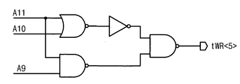
FIGS. 4 a and 4 b, it will be described embodiments of a decoding circuit applied to tWR. - If an undefined address signal is applied in case of applying to tWR, the circuit outputs tWR set with a specific value. That is, with reference to
FIG. 1 a, if address signals A11, A10, A9 are applied to (0, 0, 0), (1, 1, 0), or (1, 1, 1), the decoding circuit outputs tWR with a specific value. - Here, the tWR with a specific value represents one of values corresponding to the tWR function. For instance, it is preferable to set the tWR with “5”(tAA=15 nsec=tCK*CL) to embody function of DDR667 model of semiconductor memories which have 3 nsec for a clock period. Therefore,
FIGS. 4 a and 4 b, as embodiments, explain that the tWR is set with “5” if an undefined address signal is applied. That is, in applying the embodiment, DDR667 model of semiconductor memories is designed to be operated in the state of tWR=5 when an undefined address signal is applied. -
FIG. 4 a is an embodiment for a case of tWR=5 corresponding to the undefined address signal, andFIG. 3 b is an equivalent circuit diagram withFIG. 3 a. The decoding circuit can be designed with various schemes except those inFIGS. 4 a and 4 b. - The decoding circuit in
FIG. 4 a is configured by a logical circuit to output tWR=5 when an undefined address signal is applied, and the logical circuit is comprised of NOR gate, NAND gate, and inverter. - A first NOR gate receives and NOR-combines address signals A9, A10, and the NAND gate receives and NAND-combines address signals A9, A11. A first inverter inverts an output from the NAND gate, and a second NOR gate receives and NOR-combines an output from the first NOR gate and an output from the first inverter. A second inverter outputs an output from the second NOR gate by inverting it.
- According to the combinations, if the address signals A11, A10, A9 are (0, 0, 0), (1, 0, 0), (1, 1, 0), (1, 1, 1), the tWR is set with “5” in the embodiment according to the present invention.
- Therefore, a semiconductor device to which applies the embodiment in accordance with the present invention is operated in a state to set tWR with a specific value even when an undefined address signals is applied.
- It is possible to set tWR with various values except setting by tWR=5 according to the semiconductor device in accordance with the present invention.
-
FIG. 4 b is an equivalent circuit withFIG. 4 a, and thus possible to change to various circuits with the same function to the circuit inFIG. 4 a. - As aforementioned, the present invention shows a decoding circuit about CL and tWR with reference to preferred embodiments. However, the present invention can be utilized variously in case of embodying a predetermined decoding circuit by using an address signal without being limited aforementioned cases.
- Furthermore, if an undefined address signal is applied, the present invention has suggested embodiments set by CL=5 and tWR=5, but CL and tWR can be set with various cases by necessity.
- As apparent from the above description, the present invention provides a decoding circuit for a memory device. As a result, in performing a decoding operation using an address signal, the present invention lets the decoded result for an undefined value have a specific value, which leads the semiconductor device to be stabilized by performing function corresponding to the specific value. Especially, it is advantageous to prevent an over current flow and stabilize an operation by applying to functions of CL and tWR.
- In the drawings and specification, there have been disclosed typical preferred embodiments of the invention and, although specific terms are employed, they are used in a generic and descriptive sense only and not for purposes of limitation, the scope of the invention being set forth in the following claims.
Claims (8)
Applications Claiming Priority (2)
| Application Number | Priority Date | Filing Date | Title |
|---|---|---|---|
| KR1020030065106A KR100668820B1 (en) | 2003-09-19 | 2003-09-19 | A decoding circuit receiving address signals of a memory device |
| KR2003-65106 | 2003-09-19 |
Publications (2)
| Publication Number | Publication Date |
|---|---|
| US20050063243A1 true US20050063243A1 (en) | 2005-03-24 |
| US7184357B2 US7184357B2 (en) | 2007-02-27 |
Family
ID=34309455
Family Applications (1)
| Application Number | Title | Priority Date | Filing Date |
|---|---|---|---|
| US10/941,552 Active US7184357B2 (en) | 2003-09-19 | 2004-09-15 | Decoding circuit for memory device |
Country Status (2)
| Country | Link |
|---|---|
| US (1) | US7184357B2 (en) |
| KR (1) | KR100668820B1 (en) |
Cited By (2)
| Publication number | Priority date | Publication date | Assignee | Title |
|---|---|---|---|---|
| US20050111265A1 (en) * | 2001-10-15 | 2005-05-26 | Renesas Technology Corp. | Semiconductor device using SCL circuit |
| CN107025932A (en) * | 2015-12-01 | 2017-08-08 | 爱思开海力士有限公司 | Memory and the electronic installation including it |
Citations (5)
| Publication number | Priority date | Publication date | Assignee | Title |
|---|---|---|---|---|
| US5673233A (en) * | 1996-02-16 | 1997-09-30 | Micron Technology, Inc. | Synchronous memory allowing early read command in write to read transitions |
| USRE37273E1 (en) * | 1995-08-31 | 2001-07-10 | Fujitsu Limited | Synchronous semiconductor device with discontinued functions at power down |
| US6337809B1 (en) * | 1999-04-06 | 2002-01-08 | Samsung Electronics, Co., Ltd. | Semiconductor memory device capable of improving data processing speed and efficiency of a data input and output pin and related method for controlling read and write |
| US6483579B2 (en) * | 1999-05-14 | 2002-11-19 | Nec Corporation | Clock synchronization semiconductor memory device |
| US6489819B1 (en) * | 1998-10-27 | 2002-12-03 | Mitsubishi Denki Kabushiki Kaisha | Clock synchronous semiconductor memory device allowing testing by low speed tester |
-
2003
- 2003-09-19 KR KR1020030065106A patent/KR100668820B1/en active IP Right Grant
-
2004
- 2004-09-15 US US10/941,552 patent/US7184357B2/en active Active
Patent Citations (5)
| Publication number | Priority date | Publication date | Assignee | Title |
|---|---|---|---|---|
| USRE37273E1 (en) * | 1995-08-31 | 2001-07-10 | Fujitsu Limited | Synchronous semiconductor device with discontinued functions at power down |
| US5673233A (en) * | 1996-02-16 | 1997-09-30 | Micron Technology, Inc. | Synchronous memory allowing early read command in write to read transitions |
| US6489819B1 (en) * | 1998-10-27 | 2002-12-03 | Mitsubishi Denki Kabushiki Kaisha | Clock synchronous semiconductor memory device allowing testing by low speed tester |
| US6337809B1 (en) * | 1999-04-06 | 2002-01-08 | Samsung Electronics, Co., Ltd. | Semiconductor memory device capable of improving data processing speed and efficiency of a data input and output pin and related method for controlling read and write |
| US6483579B2 (en) * | 1999-05-14 | 2002-11-19 | Nec Corporation | Clock synchronization semiconductor memory device |
Cited By (3)
| Publication number | Priority date | Publication date | Assignee | Title |
|---|---|---|---|---|
| US20050111265A1 (en) * | 2001-10-15 | 2005-05-26 | Renesas Technology Corp. | Semiconductor device using SCL circuit |
| US6954401B2 (en) * | 2001-10-15 | 2005-10-11 | Renesas Technology Corp. | Semiconductor memory device integrating source-coupled-logic (SCL) circuit into an address buffer and a decoder |
| CN107025932A (en) * | 2015-12-01 | 2017-08-08 | 爱思开海力士有限公司 | Memory and the electronic installation including it |
Also Published As
| Publication number | Publication date |
|---|---|
| KR100668820B1 (en) | 2007-01-16 |
| KR20050028614A (en) | 2005-03-23 |
| US7184357B2 (en) | 2007-02-27 |
Similar Documents
| Publication | Publication Date | Title |
|---|---|---|
| EP0929075B1 (en) | Synchronous type semiconductor memory device | |
| US7420873B2 (en) | Simplified power-down mode control circuit utilizing active mode operation control signals | |
| EP0294947A2 (en) | Semiconductor memory device with an error-checking circuit | |
| US6392909B1 (en) | Semiconductor memory device having fixed CAS latency in normal operation and various CAS latencies in test mode | |
| JPH07177015A (en) | Power cut circuit for synchronous type semiconductor device | |
| KR20170109026A (en) | Methods and Apparatus for Command Shifter Reduction | |
| JPH07192470A (en) | Output circuit for semiconductor memory | |
| JP4419074B2 (en) | Semiconductor memory device | |
| KR100493028B1 (en) | Circuit and method of generating mode register set(MRS) code in semiconductor memory device | |
| US6483772B2 (en) | Semiconductor memory device capable of masking data to be written | |
| JP2004265484A (en) | Semiconductor memory device | |
| JP3725270B2 (en) | Semiconductor device | |
| US6337814B1 (en) | Semiconductor memory device having reference potential generating circuit | |
| US7184357B2 (en) | Decoding circuit for memory device | |
| KR100853469B1 (en) | Semiconductor memory device | |
| JP2006351108A (en) | Semiconductor storage device | |
| US7898883B2 (en) | Method for controlling access of a memory | |
| US8427883B2 (en) | Setting circuit and integrated circuit including the same | |
| US6934216B2 (en) | Semiconductor memory device | |
| US11646066B2 (en) | Memory controller and related memory | |
| US6845040B2 (en) | Nonvolatile memory | |
| US8009497B2 (en) | Auto-refresh control circuit and a semiconductor memory device using the same | |
| JP3642420B2 (en) | Semiconductor device | |
| KR100288417B1 (en) | Synchronous type semiconductor memory device | |
| JP2005294713A (en) | Semiconductor integrated circuit |
Legal Events
| Date | Code | Title | Description |
|---|---|---|---|
| AS | Assignment |
Owner name: HYNIX SEMICONDUCTOR INC., KOREA, REPUBLIC OF Free format text: ASSIGNMENT OF ASSIGNORS INTEREST;ASSIGNOR:AN, YONG BOK;REEL/FRAME:015806/0448 Effective date: 20040906 |
|
| STCF | Information on status: patent grant |
Free format text: PATENTED CASE |
|
| FEPP | Fee payment procedure |
Free format text: PAYOR NUMBER ASSIGNED (ORIGINAL EVENT CODE: ASPN); ENTITY STATUS OF PATENT OWNER: LARGE ENTITY |
|
| FEPP | Fee payment procedure |
Free format text: PAYER NUMBER DE-ASSIGNED (ORIGINAL EVENT CODE: RMPN); ENTITY STATUS OF PATENT OWNER: LARGE ENTITY |
|
| FEPP | Fee payment procedure |
Free format text: PAYOR NUMBER ASSIGNED (ORIGINAL EVENT CODE: ASPN); ENTITY STATUS OF PATENT OWNER: LARGE ENTITY |
|
| FPAY | Fee payment |
Year of fee payment: 4 |
|
| FPAY | Fee payment |
Year of fee payment: 8 |
|
| MAFP | Maintenance fee payment |
Free format text: PAYMENT OF MAINTENANCE FEE, 12TH YEAR, LARGE ENTITY (ORIGINAL EVENT CODE: M1553) Year of fee payment: 12 |