US20050081175A1 - Method for discrete gate sizing in a netlist - Google Patents
Method for discrete gate sizing in a netlist Download PDFInfo
- Publication number
- US20050081175A1 US20050081175A1 US10/683,628 US68362803A US2005081175A1 US 20050081175 A1 US20050081175 A1 US 20050081175A1 US 68362803 A US68362803 A US 68362803A US 2005081175 A1 US2005081175 A1 US 2005081175A1
- Authority
- US
- United States
- Prior art keywords
- gates
- size
- nodes
- gate
- driver
- Prior art date
- Legal status (The legal status is an assumption and is not a legal conclusion. Google has not performed a legal analysis and makes no representation as to the accuracy of the status listed.)
- Abandoned
Links
Images
Classifications
-
- G—PHYSICS
- G06—COMPUTING; CALCULATING OR COUNTING
- G06F—ELECTRIC DIGITAL DATA PROCESSING
- G06F30/00—Computer-aided design [CAD]
- G06F30/30—Circuit design
- G06F30/32—Circuit design at the digital level
- G06F30/327—Logic synthesis; Behaviour synthesis, e.g. mapping logic, HDL to netlist, high-level language to RTL or netlist
Definitions
- the present invention relates generally to gate sizing in integrated circuit design and more particularly to a novel apparatus and method for network-based gate sizing in standard cell design.
- one parameter relating to the ability of a driver transistor to charge or discharge a load, C L is the channel width of the driver transistor which determines its output resistance, R, and hence the RC time constant upon which the switching speed depends.
- R the channel width of the driver transistor which determines its output resistance
- R the RC time constant upon which the switching speed depends.
- an increase in the channel width of the driver transistor decreases its output resistance, R, thereby increasing switching speed.
- a decrease the channel width of the driver transistor increases its output resistance, R, thereby decreasing switching speed.
- this driver transistor When performing a timing analysis of the integrated circuit, a faster switching speed at this driver transistor may be required to maintain timing constraints within the MOS circuit.
- One solution would be to simply to increase the channel width of this transistor, for the reasons above stated.
- this transistor may also be a load of a previous transistor in the circuit. Since increasing the channel width of a MOS transistor increases its input gate capacitance, the load seen by the previous transistor increases, thereby resulting in slower switching at the previous stage. Accordingly, timing constraints may not then be met at the previous stage.
- each gate is composed of various circuit components to implement its predefined function.
- the load, C L thus is typically the sum of each input gate capacitance, C in , seen at an input pin of the gate, when being a receiver gate switched by the driver transistor in the example above.
- Such gate also has an output pin at which the function and size of the driver transistor in the above example is found.
- each gate used in the design has previously been implemented in library, such that the components within the gate are not subject to further design variations outside of the library implementation Accordingly, selection of a gate from a library for a required size of its output transistor determines its corresponding input gate capacitance, and vice versa.
- selection of a gate from a library for a required size of its output transistor determines its corresponding input gate capacitance, and vice versa.
- the gate size is referred to as the gate size. Accordingly, timing along data paths and maintaining the requisite timing constraints becomes a problem of selecting gate sizes for each gate in the circuit.
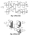
- FIG. 1 Prior Art
- the circuit 10 includes a plurality of gates 12 1-7 , for which there are known library implementations and for each one of the gates 12 1-7 several sizes are available.
- the circuit 10 it shall be assumed that for each available size for each one of the gates 12 1-7 channel width dependencies between transistors within each one of the gates 12 1-7 require that all such channel widths remain proportionally dependent within each one of the gates 12 1-7 as it is upsized or downsized. Accordingly, a larger or smaller gate size for any one of the gates 12 1-7 respectively results in a larger or smaller input capacitance and in a smaller or larger output resistance.
- gate 12 1 If the size of gate 12 1 is made larger, then its input capacitance, C in , is also made larger to due the increased channel widths in this gate. Accordingly, when gate 12 1 is a receiver gate for either the one of a previous driver gate, such as gate 12 4 or gate 12 5 , either one of these previous stages if kept the same size may be unable to switch gate 12 1 quickly enough to maintain timing constraints in the circuit 10 .
- each receiver gate 12 2 and receiver gate 12 3 are made smaller, then each of their corresponding output resistance is made smaller due to the decreased channel widths in each of these gates. Accordingly, when either of gate 12 2 or gate 12 3 is a driver gate for a subsequent receiver gate, such as gate 12 6 and gate 12 7 , neither of gate 12 2 or gate 12 3 may be unable to switch the subsequent stage if kept the same size quickly enough to maintain the timing constraints in the circuit 10 .
- ⁇ K+R ⁇ C in (1)
- K is a delay constant through the driver gate
- R is the output resistance of the driver gate
- C in is the input capacitance of the receiver gate
- slack is the difference between the required time and arrival time at the endpoint. If the arrival time is later than the required time, the difference is negative. Accordingly, negative slack on an endpoint indicates that the timing requirement is not met at that endpoint. Conversely, negative slack indicates that the actual delay on the path exceeds the required delay.
- WS worst slack of a circuit with a set, P, of paths, p
- WS - max p ⁇ P ⁇ ( PathDelay ⁇ ( p ) - RequiredDelay ⁇ ( p ) ) .
- the size of each of the gate instances in the netlist can thus be selected to optimize slack.
- the gate sizing for slack optimization can be expressed as finding a vector of gate sizes ⁇ right arrow over (x) ⁇ in a solution space, X, that minimizes a negative value of the worst slack (Eq. 2), or —WS, or min x ⁇ ⁇ X ⁇ [ max p ⁇ P ⁇ ( PathDelay ⁇ ( p ) - RequiredDelay ⁇ ( p ) ) ] . ( 4 )
- the problem may be refined by considering paths in the netlist that have worse slack than other paths, since these paths are more critical to optimize than the others, and assigning weights to timing edges in these paths.
- the timing edge in each of these paths for which its slack is the worst slack in its path may be assigned the largest weight in the path.
- the timing edge having the worst slack in the path having the worst slack of all paths may generally be assigned the largest of all weights.
- a first path may terminate at an endpoint 14 and a second path may terminate at an endpoint 16 .
- the slack, slk, at the endpoint 14 on the first path is exemplarily indicated as positive, or slk>0, showing that timing constraints are met such that the path delay is less than the required delay.
- the slack, slk, at the endpoint 16 is exemplarily indicated as negative, or slk ⁇ 0, showing otherwise.
- a timing edge 18 transitioning at the input of gate 12 3 and terminating at the input of gate 12 7 may exemplarily be identified as contributing the worst slack on the second path Accordingly, the timing edge 18 will receive the largest weight.
- the weights allow the timing edges with the largest weights to be optimized in favor over the edges with relatively lesser weights.
- the set of weights, ⁇ right arrow over (w) ⁇ , on the edges, e, at in the timing graph must satisfy a unit flow condition, i.e., at any node in the timing graph the sum of weights on all incoming edges must equal the sum of weights on all outgoing edges. Accordingly, it can be seen from the teachings of Chen, et al., in Eq. (5) that the problem of finding a set of gate sizes, ⁇ right arrow over (x) ⁇ , that minimizes worst slack, as set forth in Eq.
- a first timing edge 22 transitioning at an input 20 of gate 12 1 and extending to the input of gate 12 2 has a weight w(e 22 ) and a second timing edge 24 also transitioning at the input of gate 12 1 but extending to the input of gate 12 3 has a weight w(e 24 ). Since the second timing edge 24 is in the path terminating at endpoint 16 and further since this path has a higher criticality as set forth above, the weight w(e 24 ) on timing edge 24 is therefore larger than the weight w(e 22 ) on timing edge 24 . To minimize the sum of weighted delays as set forth in Eq. (6), the delay on timing edge 24 , delay(e 24 ), would need to be minimize to minimize the weighted delay product in Eq. 6 for this edge 24 .
- the delay, delay(e 24 ), on timing edge 24 is known to be a function of the size of gate 12 1 and a total input capacitance, CO tot , which is the sum of each input capacitance, C in , of gate 12 2 and gate 12 3 and a wire capacitance of the net between gate 12 2 and gate 12 3 . Accordingly, the delay as expressed in Eq.
- Eq. (5) Although the weighted delay gate sizing, as set forth in Eq. (5) is easier to solve than the min/max problem set forth in Eq. (4), the solution to Eq. 4 is in the continuous domain, i.e., the solution is a continuum of gate sizes for each gate and does not result in a set of gate sizes that are obtainable from a library. Accordingly, Eq. (5) cannot be used directly for the standard cell methodology, in which for each gate instance in the netlist, one or more discrete gate sizes are available for selection, as discussed above.
- standard cell methodology is the primary methodology used for the design of complex integrated circuits, especially application specific integrated circuits (ASIC's) and it is, therefore, highly desirous to obtain a gate sizing solution in this methodology that minimizes as sum of weighted delays for gate size optimization.
- ASIC application specific integrated circuits
- FIG. 2 Prior Art
- a portion of the circuit 10 of FIG. 1 including gates 12 1-3 , as described above.
- Each gate 12 1-3 is a member of a logic family, LogicFamily, and in each logic family, several gate sizes, x gate , are available from the library, such that x gate ⁇ LogicFamily.
- a solution may then be obtained for Eq. (5) in the continuous domain, and data obtained relating specifically to the continuous sizes of gate 12 1 and gate 12 3 on timing edge 24 .
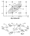
- FIG. 3 Prior Art
- a graph for the continuous domain solution with continuous sizes x 12 3 for gate 12 3 on the ordinate and continuous sizes x 12 1 for gate 12 1 on the abscissa The data obtained for an exemplary solution to Eq. 5 for timing edge 24 may result in a series of contours 26 about a locus 28 .
- the locus 28 represents an optimal solution for gates sizes x 12 1 and x 12 3 in the continuous domain, and the contours 26 represent increasingly less desirable solutions for each increasing size of the contours 26 outward from the locus 28 .
- gate 12 1 and gate 12 3 are their discrete gate sizes x 12 1 and x 12 3 , as respectively set forth in Eq. (9) and Eq. (10).
- a continuous domain solution is used to enter the discrete domain by rounding off the optimal gate sizes, as indicated at the locus 28 , to the nearest discrete gate sizes.
- the slope between the locus 28 and data point 32 is far lesser in that only two contours 26 are crossed.
- a method to select a set of gate sizes for a netlist having a plurality of gates wherein for each of the gates a number of discrete gate sizes is available for selection such that the selection minimizes worst slack in the netlist includes the steps of selecting a current first gate size for each one of the gates, performing a static timing analysis to determine slack, assigning a current weight to each one of the timing edges in the netlist based on the results of the timing analysis, selecting a new gate size for each one of the gates from one of the current gate size and a second gate size from the available gates sizes wherein such selection of each new gate size minimizes a sum of weighted delays obtained over all timing edges, and re-iterating each of the forgoing steps until an exit criteria is determined.
- the current gate size selecting step the current gate size is selected to be an initially selected on of the available gate sizes
- an at each subsequent iteration of the selecting step the current gate size for each of the gates is the new gate size for each corresponding one of the gates from an immediately prior iteration.
- the current weight assigned to each edge may be determined from a current worst slack determined from the timing analysis using the current gate size.
- the second gate size alternates between a next larger size and a next smaller size in successive iterations.
- the set of gate sizes selected from the forgoing method is the set from the iteration for which the current worst slack is determined to be minimal.
- a method to obtain the minimum sum of weighted delays in the netlist for a set of gates wherein for each gate only the first gate size and the second gate size are considered includes defining for the netlist an equivalent flow graph, computing a value of a first attribute for each node in the flow graph wherein each node corresponds to one of the gates in the netlist, and computing a value of a second attribute for each arc between a pair of nodes in the flow graph wherein each arc corresponds to the timing edges between each pair of gates to which the pair of nodes corresponds.
- the second attribute is assigned as a flow capacity for the arc for which it was computed.
- the method continues with placing a source arc between a source node and each node for which its first attribute is positive and placing a sink arc between a sink node and each node for which its first capacity attribute is negative. For each source arc its flow capacity is assigned the computed value of the first attribute of the node to which it is placed, and for each sink arc its flow capacity is assigned the negative of the computed value of the first attribute of the node to which it is placed.
- the method further continues with partitioning the flow graph into a source partition and a sink partition such that a sum of the value of the flow capacity on all arcs cut by the partitioning is a minimum sum for all possible partitions. the method concludes with selecting for the set of gates sizes the first gate size for each of the gates for which its corresponding node is in the source partition and the second gate size for each of the gates for which its corresponding node is in the sink partition.
- the value of the first attribute for each node is determined from an assigned weight and a plurality of delay coefficients, described below, associated with each of the timing edges incoming to and outgoing from one of the gates to which each node respectively corresponds.
- the value of the second attribute for each arc between a pair of nodes is determined from the assigned weight and selected ones of the delay coefficients for each one of the timing edges between a pair of gates to which a pair of nodes corresponds.
- the delay coefficients associated with each of the timing edges are determinable from a plurality of calculated delays between a driver gate and a set of receiver gates for each combination of the driver gate being one of the first gate size and the second gate size and the set of receiver gates all being one of the first gate size and the second gate size.
- the min/max path delay expression of Eq. (4) is limited in its application to typically sized netlists due to the number of gates and the number of discrete sizes for each of the gates available from libraries.
- the time required to reach a solution may disadvantageously be so excessive such that a solution may not be possible in a reasonable time.
- the continuous minimum sum of weighted delays expression of Eq. (5) although solvable in a reasonable time, is limited in its application to discrete sizes available from a library.
- the rounding may disadvantageously select a less preferential size of driver and receiver which may further increase delay on a critical path.
- the present invention overcomes the above described disadvantages and limitations of the prior art by providing a novel discrete gate sizing method in which the minimum sum of weighted delays expression is used to solve a discrete domain problem through a reiterative process that considers only two sizes for each gate instance in each iteration.
- a feature of the present invention is that the reiterative process has an inner loop process and an outer loop process. The inner loop process is performed for each iteration of the outer loop process.
- each gate in the netlist will be one of either of the two sizes.
- a starting set of gate sizes and weights for each timing edge are assigned.
- the starting set of gate sizes relates to the solution set of gate sizes of the inner loop of a prior iteration.
- Another feature of the outer loop in another embodiment of the present invention is that the weight assigned on each edge in each iteration is refined based on the weight of the prior iteration such that the reiterative process converges quicker to a preferred solution.
- the present invention is able to optimize delays on critical paths by using the minimum sum of weighted delay expression, but advantageously apply it to the discrete domain by transforming the netlist into an equivalent flow graph for which optimization is readily obtained using well known min-cut/max flow algorithms.
- One particular advantage is that the partitioning of the flow graph to find the optimum gate size is readily achievable in a reasonable time proportional to N 3 or N 2 E time wherein N and E are number of gates and number of edges, respectively.
- FIG. 1 (Prior Art) is a block diagram of an exemplary circuit useful to describe prior art gate sizing methods
- FIG. 2 (Prior Art) is a portion of the circuit of FIG. I showing available discrete gate sizes for each gate;
- FIG. 3 (Prior Art) is a graph showing an exemplary solution to a continuous domain minimum weighted sum of delays as applied to two gates of FIG. 2 ;
- FIG. 4 is a flowchart of a novel method in which a minimum sum of weighted delays solution is transformed into a solution of a min-cut/max flow problem
- FIG. 5 is an exemplary flow graph defined in the flow graph defining step of FIG. 4 ;
- FIG. 6 is a flowchart of the method to calculate the attributes of the attribute computing steps of FIG. 4 ;
- FIG. 7 is a flowchart of the arc placing step of FIG. 4 ;
- FIG. 8 is a flowchart of the gate size selecting step of FIG. 4 ;
- FIG. 9 is a flowchart setting forth the a novel gate sizing method according to the principles of the present invention.
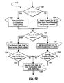
- FIG. 10 is a flowchart of the current gate size selecting step of FIG. 9 ;
- FIG. 11 is a flowchart of the current weight assigning step of FIG. 9 .
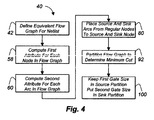
- FIG. 4 there is shown a flowchart 40 of a novel method to select a set of gate sizes for a netlist wherein for each one of the gates only one of a discrete first gate size and a discrete second gate size is available for selection such that the selection minimizes a sum of weighted delays over all timing edges in the netlist.
- the solution to the minimum sum of weighted delays is transformed into a solution of a min-cut/max flow problem.
- flowchart 40 relates to the broadest aspects of the inner loop of the reiterative process descsribed above.
- the change of capacitance, ⁇ C r , on the net is expressed as the change of input capacitance of the receiver gate, r, since the wire capacitance on the net is assumed to be constant and therefore does not contribute to the change of capacitance on the net.
- each a that contributes to A j is associated with either S drv or S r . Accordingly, each A j associated with each j th one of the gates has a component when such gate is a driver gate and when such gate is a receiver gate.
- w(e) is the weight on each one of the timing edges from an i th driver gate to a j th receiver gate
- W is the sum of assigned weights w(e) on all outgoing timing edges from the i th driver gate
- ⁇ C j is a difference in input capacitance between the second size and the first size for the j th receiver gate.
- Eq. (32) is then seen as an expression for the sum of weighted delays in Eq. (13) expressed as a function of gate size when only two sizes for each of the gates are considered.
- Eq. (32) is then seen as an expression for the sum of weighted delays in Eq. (13) expressed as a function of gate size when only two sizes for each of the gates are considered.
- the expression for the minimum sum of weighted delays becomes min S ⁇ ⁇ ⁇ 0 , 1 ⁇ N ⁇ ( ⁇ j ⁇ insts ⁇ ⁇ A j ⁇ S j + ⁇ i , j ⁇ insts ⁇ ⁇ B i , j
- ) is then seen as an expression for the sum of weighted delays in Eq. (13) expressed as a function of gate size when only two sizes for each of the gates are considered.
- the method of flowchart 40 includes a step 42 of defining for the netlist an equivalent flow graph 44 ( FIG. 5 ).
- the flow graph 44 has a plurality of first nodes 46 1 , . . . 46 i , 46 j , . . . 46 N , a plurality of first arcs 48 l,i , . . . 48 i,j , . . .
- a source node 50 a plurality of source first node 46 i corresponds to a respective i th gate instance in the netlist and each first arc 48 i,j between an i th node 46 i and a j th node 46 j corresponds to a respective timing edge e between an i th gate instance and a j th gate instance in the netlist.
- the flow graph 44 contains only one first arc 48 i,j between the i th first node 46 i and the j th first node 46 j .
- the method of flowchart 40 further includes a step 58 of computing a numerical value of the first attribute A i for each i th first node 46 i and a step 60 of computing a numerical value of the second attribute B i,j for each first arc 48 i,j .
- the first attribute A i was associated with the i th gate instance and the second attribute B i,j was associated with the timing edge between the i th gate instance and the j th gate instance.
- the first attribute A i associated with the i th gate instance and second attribute associated with the timing edge between the i th and j th gate instances can now have a numerical value associated with each i th first node 46 i and each first arc 48 i,j , respectively, because of the above stated relationships between nodes and arcs in the flow graph 44 and gate instances and timing edges in the netlist.
- the value of the first attribute A i is determinable from an assigned weight w(e) and numerical values of a plurality of delay coefficients on each timing edge e outgoing from and incoming to an i th gate instance corresponding to each i th first node 46 i , wherein the value of the delay coefficients is obtained for each case of delay(S drv , ⁇ right arrow over (S) ⁇ r ) on each timing edge e.
- the value of the second attribute B i,j for each first arc 48 i,j is determinable from the weight w(e) on the corresponding timing edges e from the i th gate instance corresponding to each i th first node 46 i and the numerical value of selected ones of the delay coefficients on the corresponding timing edge between the i th gate instance and the j th gate instance corresponding to each j th first node 46 j .
- the value of the delay coefficients is obtained for each case of delay(S drv , ⁇ right arrow over (S) ⁇ r ) on each timing edge e in the netlist from an i th gate instance. Since four cases of delay(S drv , ⁇ right arrow over (S) ⁇ r ) exist, the delay coefficients may, in one embodiment of the present invention, specifically include a first coefficient, a second coefficient, a third coefficient and a fourth coefficient as set forth immediately below.
- the first attribute A k at any k th gate instance includes the summation of each A i incr set forth in Eq. (33) for each outgoing timing edge from the k th gate instance, being a driver gate, and the summation of each A i incr set forth in Eq. (34) for each incoming timing edge to the k th gate instance being a receiver gate. Since the k th first node 46 k corresponds to the k th gate instance, the numerical value of the first attribute A k associated with the k th first node 46 k may be computed from an expression for A k associated with the k th gate instance.
- a numerical value of the first increment A k for the k th first node 46 k may be computed from the expressions for A i incr and A j incr set forth above in Eq.'s (33) and (34), respectively, wherein at any k th first node 46 k , the total sum of its incremental values A i incr obtained when such k th first node 46 k , was an i th first node 46 i (corresponding to the i th driver gate instance) are summed together with a total sum of its incremental values A j incr obtained when such k th first node 46 k , was a j th first node 46 j (corresponding to the j th receiver gate instance).
- a numerical value of the second attribute B i,j for each first arc 48 i,j may, in a preferred embodiment of the present invention, be computed from the expression for B i,j set forth in Eq. (35).
- the expression of Eq. (35) is used to obtain an incremental value for each such timing edge and each incremental value summed to obtain the value of the second attribute B i,j for each first arc 48 i,j .
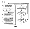
- FIG. 6 there is shown a flowchart 62 that sets forth a preferred re-iterative method for computing the value of the first attribute A i at each i th first node 46 i and the value of the second attribute B i,j for each first arc 48 i,j , as generally set forth above in the description of steps 58 and 60 of FIG. 4 .
- the method of flowchart 62 includes a step 64 of calculating a numerical value of the delay delay(e) on each timing edge e transitioning from the corresponding i th gate instance for each case of delay(S drv , ⁇ right arrow over (S) ⁇ r ).
- Each case of the delay is preferably calculated from library timing models for each of the first and second gate sizes of the i th driver gate instance and the set of j th receiver gate instances.
- the method of flowchart 62 further includes, at each i th iteration, a step 66 of calculating a value of each of the first, second, third and fourth delay coefficients for each timing edge e transitioning from the i th gate instance.
- the method of flowchart 62 further includes a step 68 of calculating a value of the first increment A i incr described above for each i th first node 46 i .
- the value of A i incr is preferably computed from the expression of Eq. (33) and from the values of the calculated delay coefficients obtained in the present i th iteration of step 66 above.
- the method of flowchart 62 further includes a step 70 of calculating a value of the second increment A j incr described above for each j th first node 46 j .
- the value of A j incr is obtained the expression of Eq. (34) and from the values of the calculated delay coefficients obtained in step 66 above for the present i th iteration.
- the values of the first increment A i incr and the second increment A j incr accumulate at each first node 46 so that a resultant value of the first attribute A k accumulates at any k th first node 46 k .
- the method of flowchart 62 further includes a step 72 of calculating a value of the second attribute B i,j for each first arc 48 i,j outgoing from the current i th first node 46 i .
- the value of B i,j is obtained from the expression of Eq. (35) and the values of the delay coefficients obtained in step 66 above in the present i th iteration.
- step 76 a determination is made, whether in the present i th iteration there is another j th first node 46 j . If YES, step 68 , step 70 , step 72 and step 74 are reiterated for the next j th first node 46 j .
- step 78 a determination is made whether i ⁇ N. If YES, step 64 and all subsequent steps of flowchart 62 are performed as above for the next i th +1 iteration. If NO, the next step of flowchart 40 ( FIG. 4 ) is performed.
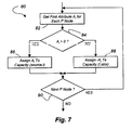
- the next step in the method of the flowchart 40 is the step 80 of placing the source arcs 52 src,i and sink arcs 56 i,snk in the flow graph 44 .
- each source arc 52 src,i is placed between the source node 50 and each respective i th first node 46 i for which the accumulated value of its first attribute A i is positive.
- each sink arc 56 i,snk is placed between the sink node 54 and each respective i th first node 46 i for the accumulated value of its first attribute A 1 is negative.
- the flow capacities, capacity(source, i) and capacity(i, sink) are then assigned based on the value of the first attribute of the i th first node 46 i .
- step 80 A preferred implementation of the step 80 is shown in FIG. 7 .
- step 84 a decision is made whether A i >0.
- a source arc 52 src,i is placed between the source node 50 and the i th first node 46 i .
- a sink arc 56 i,snk is placed between the i th first node 46 i and the sink node 54 .
- step 90 a decision is made whether i ⁇ N. If YES, an iteration for the next i th node 46 i commences at step 82 . If NO, the next step of flowchart 40 is performed.
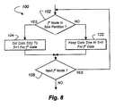
- the method of flowchart 40 further includes a step 92 of partitioning the first nodes 46 l , . . . 46 i , 46 j , . . . 46 N into a source partition 94 and a sink partition 96 , as best seen in FIG. 5 .
- the partitioning is made by a cut, as indicated at 98 , such that a sum of the value of the capacity on each of the source arcs 52 src,1 , . . . 52 src,i , sink arcs 56 j,snk , . . . 56 N,snk and first arcs 48 l,i , . . . 48 i,j , . . .
- Eq. (36) is an equivalent to a min-cut/max flow problem for solvable using a Push-Relabel algorithm for which a solution may be found in N 3 or N 2 E time as in known in the art and specifically taught by Cherkassky, et. al., On Implementing Push - Relabel Algorithm for the Maximum Flow Problem, Algorithmica, vol. 19, pp.'s 390-410, 1997.
- a Push-Relabel algorithm is used to obtain the cut 98 .
- the method of flowchart 40 concludes with a step 100 of selecting the current, or first, gate size for each j th gate for which the corresponding j th first node 46 j is in the source partition 94 .
- the step 100 also includes selecting the second size for each j th gate for which the corresponding j th first node 46 j is in the sink partition 96 .
- the set of gate sizes resulting from this step 100 satisfies Eq. (35).
- step 102 a decision is made whether the current j th first node 46 j is in the sink partition 96 .
- step 104 the j th instance of the gate corresponding to the j th node 46 j is selected to be the second size. Otherwise, if the decision is NO, then at step 106 the j th instance of the gate corresponding to the j th node 46 j is selected to be the current or first size.
- step 108 a decision is made whether j ⁇ N. If YES, an iteration for the next j th node 46 j commences at step 102 . If NO, the solution to Eq. (36) has been obtained.
- a practical netlist uses libraries for gates for which there are more than two sizes.
- the following description sets forth a method in which the two gate size methods described above are applicable.
- a series of iterations using all the available gate sizes may be performed wherein only two of the gate sizes in each iteration are used as above.
- a resultant set of gate sizes from the those two gate sizes that satisfies Eq. (36) is obtained.
- all gate sizes from the prior iteration are resized either up or down, and the two gate size method described above is re-performed.
- a set of gate sizes that satisfies Eq. (4) may be determined.
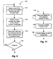
- FIG. 9 there is shown a flowchart 110 of a reiterative process for a method to select a set ⁇ right arrow over (x) ⁇ of gate sizes for a netlist having N number of gates wherein for each i th one of the gates a predetermined number of discrete gates sizes X 1 is available for selection.
- the set ⁇ right arrow over (x) ⁇ of gate sizes selected is chosen to minimize worst slack in the netlist. Accordingly, the set ⁇ right arrow over (x) ⁇ of gate sizes may be selected to satisfy the expression of Eq. (4).
- each iteration of the method of flowchart 110 includes a step 112 of selecting a current first gate size X for each instance insts of the gates and an available second gate size for each instance.
- the current first gate size X for each instance is selected to be an initially selected one of the available library gate sizes.
- the current first gate size X for each instance is selected to be a resultant gate size for the same instance from an immediately prior iteration of the flowchart 110 , as described below.
- the availability of the second gate size from the library for each instance is used in a subsequent step described below.
- the method of flowchart 110 includes a step 114 of performing a timing analysis and assigning a set of weights ⁇ right arrow over (w) ⁇ .
- Each current weight w(e) in the set of weights ⁇ right arrow over (w) ⁇ is associated with a respective timing edge e in the netlist.
- the timing analysis determines slack and worst slack in the netlist.
- the current weight w(e) is a function of a current worst slack determined for the netlist using the current first gate size.
- the method of flowchart 110 includes the step of selecting a new gate size X for each instance insts of the gates from the current first gate size and the second gate size identified above such that the set of new gate sizes obtains a minimum sum of weighted delays.
- the step 116 is preferable performed in accordance with the above described method of FIG. 4 wherein the minimum sum of weighted delays is obtained as a solution to a min-cut problem using the two gate sizes. Accordingly, in one embodiment of the present invention the set of new gate sizes resulting from the performance of step 116 satisfies the expression of Eq. (36).
- a YES decision at step 118 indicates that an exit criteria has been determined.
- the set ⁇ right arrow over (x) ⁇ of gate sizes X is selected from the iteration for which the current worst slack was determined at step 114 to be minimal.
- the exit criteria can be based upon various factors, such as a total number of iterations, or that each successive iteration indicates that the set of weights begins to converge, as is described in greater detail below, indicating that path delays have been optimized or that worst slack cannot be further improved.
- a total number of iterations can be based upon a maximum number or some other number relating to the largest maximum number of gate sizes available for any one instance.
- step 132 If the second size is selected to be the next larger size at step 128 , an inquiry is made, as indicated at step 132 whether for each i th gate instance such next larger size is available. If YES, then processing continues to the weight assigning step 114 of FIG. (9) described above.
- step 130 an inquiry is made, as indicated at step 134 whether for each i th gate instance such next smaller size is available. If YES, then processing continues to the weight assigning step 114 of FIG. (9) described above.
- step 132 or step 134 determines whether the second size is available in the library. If the decision at step 132 or step 134 is NO, then, as indicated at step 135 , for any i th gate instance for which the second size is not available in the library, then for any such i th gate instance the first gate size will be maintained throughout the performance of new gate selecting step 116 .
- the timing analysis and weight assigning step 114 of FIG. 9 there is shown a preferred embodiment of the timing analysis and weight assigning step 114 of FIG. 9 .
- a static timing analysis to determine slack is well known and need not be further described.
- the weight w(e) for each associated timing edge e may be determined as a function of slack on each associated timing edge e and worst slack.
- the weight w(e) on each associated timing edge e is normalized. Accordingly, at each one of the gates a sum of said weight w(e) on each incoming timing edge e is equal to a sum of said weight w(e) on each outgoing timing edge e.
- weight w(e) for each associated timing edge e is updated as a function of a prior weight assigned in an immediately prior iteration at a same one of each associated timing edge e. Updating of weights allows the weights on each edge to converge faster resulting in fewer iterations of the method of FIG. 9 .
Abstract
A set of gate sizes for a netlist having a plurality of gates wherein for each of the gates a number of discrete gate sizes is available is selected such that the selection minimizes worst slack in the netlist. A current gate size for each gate is selected and an a current weight assigned to each one of the timing edges in the netlist. A new gate size is selected for each one of the gates from one of the current gate size and second one of the available gates sizes wherein such selection of each new gate size minimizes a sum of weighted delays obtained over all timing edges. The minimum sum of weighted delays is obtained from a min-cut in a timing flow graph. The results of the min-cut are used in the next iteration and re-iterating occurs until an exit criteria is determined.
Description
- The present invention relates generally to gate sizing in integrated circuit design and more particularly to a novel apparatus and method for network-based gate sizing in standard cell design.
- In a MOS integrated circuit, one parameter relating to the ability of a driver transistor to charge or discharge a load, CL, is the channel width of the driver transistor which determines its output resistance, R, and hence the RC time constant upon which the switching speed depends. For a constant load, CL, an increase in the channel width of the driver transistor decreases its output resistance, R, thereby increasing switching speed. Conversely, for the same load, CL, a decrease the channel width of the driver transistor increases its output resistance, R, thereby decreasing switching speed.
- When performing a timing analysis of the integrated circuit, a faster switching speed at this driver transistor may be required to maintain timing constraints within the MOS circuit. One solution would be to simply to increase the channel width of this transistor, for the reasons above stated. However, this transistor may also be a load of a previous transistor in the circuit. Since increasing the channel width of a MOS transistor increases its input gate capacitance, the load seen by the previous transistor increases, thereby resulting in slower switching at the previous stage. Accordingly, timing constraints may not then be met at the previous stage.
- In the design of the data paths in a reasonably sized MOS integrated circuit, the smallest component design is generally a logic stage or standard cell, hereinafter referred to as a gate. Each gate is composed of various circuit components to implement its predefined function. The load, CL, referred to above thus is typically the sum of each input gate capacitance, Cin, seen at an input pin of the gate, when being a receiver gate switched by the driver transistor in the example above. Such gate, of course, also has an output pin at which the function and size of the driver transistor in the above example is found.
- Typically, each gate used in the design has previously been implemented in library, such that the components within the gate are not subject to further design variations outside of the library implementation Accordingly, selection of a gate from a library for a required size of its output transistor determines its corresponding input gate capacitance, and vice versa. Typically to provide design flexibility, for each gate in one logical family several variations of the gate are available from the library. Each of these variations for one particular gate is referred to as the gate size. Accordingly, timing along data paths and maintaining the requisite timing constraints becomes a problem of selecting gate sizes for each gate in the circuit.
- For example, in
FIG. 1 (Prior Art) there is shown asimple MOS circuit 10, which may be a portion of a much larger circuit. Thecircuit 10 includes a plurality ofgates 12 1-7, for which there are known library implementations and for each one of thegates 12 1-7 several sizes are available. For purposes of thisexemplary circuit 10, it shall be assumed that for each available size for each one of thegates 12 1-7 channel width dependencies between transistors within each one of thegates 12 1-7 require that all such channel widths remain proportionally dependent within each one of thegates 12 1-7 as it is upsized or downsized. Accordingly, a larger or smaller gate size for any one of thegates 12 1-7 respectively results in a larger or smaller input capacitance and in a smaller or larger output resistance. - Should the results of a timing analysis indicate that timing constraints are not met between a driver gate, such as
gate 12 1 and its receiver gates, such asgate 12 2 andgate 12 3, faster switching between the driver gate and each receiver gate would need to occur. Accordingly, either the size ofgate 12 1, as the driver gate, would need to be made larger, or the size of each ofgate 12 2 andgate 12 3, as the receiver gates, would need to be smaller. For reasons as stated above, increasing the size ofgate 12 1 decreases its output resistance allowing faster switching and decreasing the size ofgate 12 2 andgate 12 3 decreases the size of their respective input capacitance, also allowing faster switching. It may also be required thatgate 12 1 is made larger simultaneously withgate 12 2 andgate 12 3 being made smaller. - If the size of
gate 12 1 is made larger, then its input capacitance, Cin, is also made larger to due the increased channel widths in this gate. Accordingly, whengate 12 1 is a receiver gate for either the one of a previous driver gate, such asgate 12 4 orgate 12 5, either one of these previous stages if kept the same size may be unable to switchgate 12 1 quickly enough to maintain timing constraints in thecircuit 10. - Similarly, if the size of each
receiver gate 12 2 andreceiver gate 12 3 are made smaller, then each of their corresponding output resistance is made smaller due to the decreased channel widths in each of these gates. Accordingly, when either ofgate 12 2 orgate 12 3 is a driver gate for a subsequent receiver gate, such asgate 12 6 andgate 12 7, neither ofgate 12 2 orgate 12 3 may be unable to switch the subsequent stage if kept the same size quickly enough to maintain the timing constraints in thecircuit 10. - In addition to the switching speed between the driver gate and each receiver gate, there also exists a timing delay through the driver gate. Since switching speed is an inverse of delay, a total delay, τ, between the input of a driver gate to the input of each receiver gate may be expressed as
τ=K+RΣC in (1)
wherein K is a delay constant through the driver gate, R is the output resistance of the driver gate and Cin is the input capacitance of the receiver gate. It is apparent from the above discussion that the delay constant K and the output resistance R are dependent upon the driver gate size, xdrv and each input capacitance Cin is dependent upon the receiver gate size xr. - It is readily seen from Eq. (1) that when selecting the size for each one of the
gates 12 1-7 in thecircuit 10 to meet timing constraints, several parameters need be considered. In a simple circuit, such as theexemplary circuit 10, the selection of gate size for each of thegates 12 1-7 may be accomplished without much difficulty. However, even an optimization of timing obtained for each possible combination of sizes for thegates 12 1-7 could be unduly burdensome should many such sizes exist for each of thegates 12 1-7. Because of the interdependencies each of these parameters have in regards to timing within each gate and between gates, it may be appreciated by those skilled in the art that as the number of gates in an integrated circuit increases, the complexity of selecting gate sizes for each of thegates 12 1-7 accordingly increases. - In the prior art, the design of a complex integrated circuit is generally defined by a netlist, which is a set of data used by design automation tools. The problem of determining the optimal size of each instance of a gate in the netlist has been addressed by analyzing the slack on all of the endpoints in a circuit. As is known, slack is the difference between the required time and arrival time at the endpoint. If the arrival time is later than the required time, the difference is negative. Accordingly, negative slack on an endpoint indicates that the timing requirement is not met at that endpoint. Conversely, negative slack indicates that the actual delay on the path exceeds the required delay.
- It then follows that the worst slack, WS, of a circuit with a set, P, of paths, p, may be expressed as a difference of path delay, PathDelay(p), and required delay RequiredDelay(p), or:
The path delay, PathDelay(p), on any path, p, is in turn defined as the sum of each timing edge delay, delay(e), on all of the timing edges, e, in such path, or
wherein a timing edge, e, transitions at an input of a driver gate and extends to the input of a receiver gate, as best seen inFIG. 1 . Since the delay, delay(e), on each edge, e, is then know to be dependent upon the size of the driver gate and each receiver gate, as described above with reference to Eq. (1), the size of each of the gate instances in the netlist can thus be selected to optimize slack. Accordingly, the gate sizing for slack optimization can be expressed as finding a vector of gate sizes {right arrow over (x)} in a solution space, X, that minimizes a negative value of the worst slack (Eq. 2), or —WS, or - In a typical netlist, a solution to the min/max problem of Eq. 4 is extremely difficult to obtain due to the large number of paths and number of gate instances in the netlist compounded by all of the possible combinations of gate sizes for each of the gate instances. For a typical netlist, a solution to Eq. (4) may not be readily obtainable in a reasonable time.
- The problem may be refined by considering paths in the netlist that have worse slack than other paths, since these paths are more critical to optimize than the others, and assigning weights to timing edges in these paths. The timing edge in each of these paths for which its slack is the worst slack in its path may be assigned the largest weight in the path. Similarly, the timing edge having the worst slack in the path having the worst slack of all paths may generally be assigned the largest of all weights.
- For example, in
FIG. 1 a first path may terminate at anendpoint 14 and a second path may terminate at anendpoint 16. The slack, slk, at theendpoint 14 on the first path is exemplarily indicated as positive, or slk>0, showing that timing constraints are met such that the path delay is less than the required delay. However, the slack, slk, at theendpoint 16 is exemplarily indicated as negative, or slk<0, showing otherwise. Atiming edge 18 transitioning at the input ofgate 12 3 and terminating at the input ofgate 12 7 may exemplarily be identified as contributing the worst slack on the second path Accordingly, thetiming edge 18 will receive the largest weight. The weights allow the timing edges with the largest weights to be optimized in favor over the edges with relatively lesser weights. However, it can be readily appreciated by those skilled in the art that obtaining a direct solution to the min/max problem of Eq. 4 for various combinations of gate sizes along each timing edge in the typical netlist, even when first considering the most critical edges first, remains computationally intensive. - As taught in Chen, et al., Fast and Exact Simultaneous Gate and Wire Sizing By Lagrangian Relaxation, Proceedings of the 1998 IEEE/ACM International Conference on Computer Aided Design (ICCAD-98), pp 617-624, ACM/IEEE, November 1998, the min/max problem of Eq. 4 may be solved in a continuous domain after being converted to the following form using Lagrangian relaxation:
wherein E is a set of edges, e, in the timing graph, and w(e) is a weight associated the timing edge, e. As described in Chen, et al., the set of weights, {right arrow over (w)}, on the edges, e, at in the timing graph must satisfy a unit flow condition, i.e., at any node in the timing graph the sum of weights on all incoming edges must equal the sum of weights on all outgoing edges. Accordingly, it can be seen from the teachings of Chen, et al., in Eq. (5) that the problem of finding a set of gate sizes, {right arrow over (x)}, that minimizes worst slack, as set forth in Eq. (4) becomes a problem of finding a set of gate sizes, {right arrow over (x)}, that minimizes a sum of the weighted delays expressed in Eq. (5) as follows: - The use of the minimum sum of weighted delays to optimize gate size can qualitatively be set forth with reference to
FIG. 1 . For example, afirst timing edge 22 transitioning at aninput 20 ofgate 12 1 and extending to the input ofgate 12 2 has a weight w(e22) and asecond timing edge 24 also transitioning at the input ofgate 12 1 but extending to the input ofgate 12 3 has a weight w(e24). Since thesecond timing edge 24 is in the path terminating atendpoint 16 and further since this path has a higher criticality as set forth above, the weight w(e24) on timingedge 24 is therefore larger than the weight w(e22) on timingedge 24. To minimize the sum of weighted delays as set forth in Eq. (6), the delay on timingedge 24, delay(e24), would need to be minimize to minimize the weighted delay product in Eq. 6 for thisedge 24. - From the above discussion, the delay, delay(e24), on timing
edge 24 is known to be a function of the size ofgate 12 1 and a total input capacitance, COtot, which is the sum of each input capacitance, Cin, ofgate 12 2 andgate 12 3 and a wire capacitance of the net betweengate 12 2 andgate 12 3. Accordingly, the delay as expressed in Eq. (1) can be rewritten for any timing edge, e, as a function of the driver gate size, Xdrv, and total receiver capacitance, COtot, as
delay(e)=ƒ(x drv , C tot) (7)
It can therefore be seen, that the minimization of the sum of weighted delays, as set forth in Eq. (6), is dependent on gate size such that gate sizes can be obtained which minimizes delay on the heaviest of the weighted edges. - Although the weighted delay gate sizing, as set forth in Eq. (5) is easier to solve than the min/max problem set forth in Eq. (4), the solution to Eq. 4 is in the continuous domain, i.e., the solution is a continuum of gate sizes for each gate and does not result in a set of gate sizes that are obtainable from a library. Accordingly, Eq. (5) cannot be used directly for the standard cell methodology, in which for each gate instance in the netlist, one or more discrete gate sizes are available for selection, as discussed above. However, standard cell methodology is the primary methodology used for the design of complex integrated circuits, especially application specific integrated circuits (ASIC's) and it is, therefore, highly desirous to obtain a gate sizing solution in this methodology that minimizes as sum of weighted delays for gate size optimization.
- In order to solve the more practical discrete gate sizing problem, it is known in the art to first obtain a solution to Eq. (5) in the continuous domain and then use such solution as a starting point to obtain a solution in the discrete domain. Typically, the entry into the discrete domain is to round off the results of the continuous domain, which may disadvantageously lead to a result, instead of minimizing delay on a critical path, could actually result in increased delay on such path.
- For example, in
FIG. 2 (Prior Art), there is shown a portion of thecircuit 10 ofFIG. 1 , includinggates 12 1-3, as described above. Eachgate 12 1-3 is a member of a logic family, LogicFamily, and in each logic family, several gate sizes, xgate, are available from the library, such that
xgate ε LogicFamily. (8)
The logic family forgate 12 1 is exemplarily shown as having three discrete sizes,
shown asgate 12 1 x=1gate 12 3 x=2 andgate 12 1 x=3, and the logic family forgate 12 3 is exemplarily shown as having two discrete sizes,
shown asgate 12 3 x=1 andgate 12 3 x=2. It is to be understood that each gate instance may have any number of discrete sizes. A solution may then be obtained for Eq. (5) in the continuous domain, and data obtained relating specifically to the continuous sizes ofgate 12 1 andgate 12 3 on timingedge 24. - With further reference to
FIG. 3 (Prior Art), there is shown a graph for the continuous domain solution with continuous sizes x123 forgate 12 3 on the ordinate and continuous sizes x121 forgate 12 1 on the abscissa. The data obtained for an exemplary solution to Eq. 5 for timingedge 24 may result in a series ofcontours 26 about alocus 28. Thelocus 28 represents an optimal solution for gates sizes x121 and x123 in the continuous domain, and thecontours 26 represent increasingly less desirable solutions for each increasing size of thecontours 26 outward from thelocus 28. - Superimposed on the graph of
FIG. 3 , forgate 12 1 andgate 12 3 are their discrete gate sizes x121 and x123 , as respectively set forth in Eq. (9) and Eq. (10). As set forth above a continuous domain solution is used to enter the discrete domain by rounding off the optimal gate sizes, as indicated at thelocus 28, to the nearest discrete gate sizes. As visually indicated inFIG. 3 , the nearest round-off point for the discrete sizes x121 and x123 from thelocus 28 is at adata point 30 at whichgate 12 1 has a discrete size x121 =1 andgate 12 3 has a discrete size x123 =2. - It can readily be seen in the graph of
FIG. 3 that to reach the nearest round-off point atdata point 30, five of thecontours 26 are crossed and that the contours are closely spaced. Accordingly, the slope of the continuous domain solution to Eq. (5) is relatively steep between thelocus 28 anddata point 30 and, as stated above, eachcontour 26 farther away from thelocus 28 indicates an increasingly less desirable continuous domain solution. - A more preferable solution for this example would be at a
data point 32 at whichgate 12 1 has a discrete size x121 =2 andgate 12 3 has a discrete size x123 =2. As seen in the graph ofFIG. 3 , the slope between thelocus 28 anddata point 32 is far lesser in that only twocontours 26 are crossed. However, since the discrete size discrete size x121 =2 forgate 12 1 is farther from thelocus 28 than for its smaller size, the rounding used in the prior art would not select the more preferable size. - The discrete size x12
1 =2 forgate 12 1 as more preferable is also apparent from the above example described in reference toFIG. 1 . Since timingedge 24 is on the path terminating at endpoint 16 (FIG. 1 ), and this path was indicated having a higher criticality, delay on timingedge 24 would be reduced if the larger size forgate 12 1 were used instead of the smaller size suggested by rounding of the continuous domain solution. - According to the present invention, a method to select a set of gate sizes for a netlist having a plurality of gates wherein for each of the gates a number of discrete gate sizes is available for selection such that the selection minimizes worst slack in the netlist includes the steps of selecting a current first gate size for each one of the gates, performing a static timing analysis to determine slack, assigning a current weight to each one of the timing edges in the netlist based on the results of the timing analysis, selecting a new gate size for each one of the gates from one of the current gate size and a second gate size from the available gates sizes wherein such selection of each new gate size minimizes a sum of weighted delays obtained over all timing edges, and re-iterating each of the forgoing steps until an exit criteria is determined.
- At an initial iteration of the current gate size selecting step the current gate size is selected to be an initially selected on of the available gate sizes, an at each subsequent iteration of the selecting step the current gate size for each of the gates is the new gate size for each corresponding one of the gates from an immediately prior iteration. In each iteration, the current weight assigned to each edge may be determined from a current worst slack determined from the timing analysis using the current gate size. In one particular embodiment of the present invention, the second gate size alternates between a next larger size and a next smaller size in successive iterations. The set of gate sizes selected from the forgoing method is the set from the iteration for which the current worst slack is determined to be minimal.
- In one aspect of the present invention, a method to obtain the minimum sum of weighted delays in the netlist for a set of gates wherein for each gate only the first gate size and the second gate size are considered includes defining for the netlist an equivalent flow graph, computing a value of a first attribute for each node in the flow graph wherein each node corresponds to one of the gates in the netlist, and computing a value of a second attribute for each arc between a pair of nodes in the flow graph wherein each arc corresponds to the timing edges between each pair of gates to which the pair of nodes corresponds. The second attribute is assigned as a flow capacity for the arc for which it was computed. The method continues with placing a source arc between a source node and each node for which its first attribute is positive and placing a sink arc between a sink node and each node for which its first capacity attribute is negative. For each source arc its flow capacity is assigned the computed value of the first attribute of the node to which it is placed, and for each sink arc its flow capacity is assigned the negative of the computed value of the first attribute of the node to which it is placed. The method further continues with partitioning the flow graph into a source partition and a sink partition such that a sum of the value of the flow capacity on all arcs cut by the partitioning is a minimum sum for all possible partitions. the method concludes with selecting for the set of gates sizes the first gate size for each of the gates for which its corresponding node is in the source partition and the second gate size for each of the gates for which its corresponding node is in the sink partition.
- In the above method, the value of the first attribute for each node is determined from an assigned weight and a plurality of delay coefficients, described below, associated with each of the timing edges incoming to and outgoing from one of the gates to which each node respectively corresponds. Similarly, the value of the second attribute for each arc between a pair of nodes is determined from the assigned weight and selected ones of the delay coefficients for each one of the timing edges between a pair of gates to which a pair of nodes corresponds.
- The delay coefficients associated with each of the timing edges are determinable from a plurality of calculated delays between a driver gate and a set of receiver gates for each combination of the driver gate being one of the first gate size and the second gate size and the set of receiver gates all being one of the first gate size and the second gate size.
- As described above, the min/max path delay expression of Eq. (4) is limited in its application to typically sized netlists due to the number of gates and the number of discrete sizes for each of the gates available from libraries. When considering every possible combination of gate sizes, the time required to reach a solution may disadvantageously be so excessive such that a solution may not be possible in a reasonable time.
- Also as described above, the continuous minimum sum of weighted delays expression of Eq. (5), although solvable in a reasonable time, is limited in its application to discrete sizes available from a library. When rounding a continuous solution for a driver and receiver gate on a timing edge, the rounding may disadvantageously select a less preferential size of driver and receiver which may further increase delay on a critical path.
- The present invention overcomes the above described disadvantages and limitations of the prior art by providing a novel discrete gate sizing method in which the minimum sum of weighted delays expression is used to solve a discrete domain problem through a reiterative process that considers only two sizes for each gate instance in each iteration. A feature of the present invention is that the reiterative process has an inner loop process and an outer loop process. The inner loop process is performed for each iteration of the outer loop process.
- In the inner loop, the continuous minimum sum of weighted delays when considering only two possible gates sizes for each gate becomes solvable as a well known min-cut/max flow solution that is readily obtained in real time and directly applicable to the discrete domain. A feature of the inner loop is that for each gate after a solution is obtained, each gate in the netlist will be one of either of the two sizes.
- In the outer loop, a starting set of gate sizes and weights for each timing edge are assigned. One feature of the outer loop is that the starting set of gate sizes relates to the solution set of gate sizes of the inner loop of a prior iteration. Another feature of the outer loop in another embodiment of the present invention is that the weight assigned on each edge in each iteration is refined based on the weight of the prior iteration such that the reiterative process converges quicker to a preferred solution.
- The present invention is able to optimize delays on critical paths by using the minimum sum of weighted delay expression, but advantageously apply it to the discrete domain by transforming the netlist into an equivalent flow graph for which optimization is readily obtained using well known min-cut/max flow algorithms. One particular advantage is that the partitioning of the flow graph to find the optimum gate size is readily achievable in a reasonable time proportional to N3 or N2E time wherein N and E are number of gates and number of edges, respectively.
- These and other objects, advantages and features of the present invention will become readily apparent to those skilled in the art form a study of the following Description of the Exemplary Preferred Embodiments when read in conjunction with the attached Drawing and appended Claims.
-
FIG. 1 (Prior Art) is a block diagram of an exemplary circuit useful to describe prior art gate sizing methods; -
FIG. 2 (Prior Art) is a portion of the circuit of FIG. I showing available discrete gate sizes for each gate; -
FIG. 3 (Prior Art) is a graph showing an exemplary solution to a continuous domain minimum weighted sum of delays as applied to two gates ofFIG. 2 ; -
FIG. 4 is a flowchart of a novel method in which a minimum sum of weighted delays solution is transformed into a solution of a min-cut/max flow problem; -
FIG. 5 is an exemplary flow graph defined in the flow graph defining step ofFIG. 4 ; -
FIG. 6 is a flowchart of the method to calculate the attributes of the attribute computing steps ofFIG. 4 ; -
FIG. 7 is a flowchart of the arc placing step ofFIG. 4 ; -
FIG. 8 is a flowchart of the gate size selecting step ofFIG. 4 ; -
FIG. 9 is a flowchart setting forth the a novel gate sizing method according to the principles of the present invention; -
FIG. 10 is a flowchart of the current gate size selecting step ofFIG. 9 ; and -
FIG. 11 is a flowchart of the current weight assigning step ofFIG. 9 . - Referring now to
FIG. 4 , there is shown aflowchart 40 of a novel method to select a set of gate sizes for a netlist wherein for each one of the gates only one of a discrete first gate size and a discrete second gate size is available for selection such that the selection minimizes a sum of weighted delays over all timing edges in the netlist. As will become readily apparent from the following description, the solution to the minimum sum of weighted delays is transformed into a solution of a min-cut/max flow problem. Thus,flowchart 40 relates to the broadest aspects of the inner loop of the reiterative process descsribed above. - To describe the transformation of the solution of the minimum sum of weighted delays in the netlist, which may be any netlist having N number of instances, insts, of gates, it is first assumed that the current size of all gates in the netlist is initially the first size, represented as S=0 and that for each gate only the first size or the second size can be used such that any gate that is resized assumes the second size, represented as S=1. Accordingly, for each jth gate in the netlist its size Sj may be defined as
- The method of the present invention, practiced in accordance with
flowchart 40, will result in a set of gate sizes, {right arrow over (S)}, wherein
{right arrow over (S)}={S1,S2, . . . ,Sj, . . . ,SN}, (12)
which minimizes a sum of weighted delays, as set forth in Eq. (6), which when combined with Eq. (12) may be re-written as: - From Eq. (1) and Eq. (7), it follows that the delay, delay(e), on each timing edge as set forth in Eq. (1 3)can be expressed as
ƒ(x drv ,C tot)=Kx drv +RC tot. (14)
As stated above in conjunction with Eq. (1) and Eq. (7), the coefficients K and R are dependent upon the size of the driver gate for the timing edge, and that Ctot is the sum of the input capacitance, Cin, of each receiver gate on each outgoing edge from the driver gate and a wire capacitance on the net between the driver gate and receiver gates. The input capacitance, Cin, is also dependent upon the size of its receiver gate, as stated above. Accordingly, the delay on each edge can be expressed as a function of driver size and the size of the set of receiver gates, such that the delay, delay(e), can be expressed as a function of {right arrow over (S)} as
delay(e)=ƒ(S drv ,{right arrow over (S)} r), (15)
wherein Sdrv is the size of the driver gate and {right arrow over (S)}r is a vector of sizes of each receiver gate, r, in the set of receiver gates, rec, on the net, n, comprised of each outgoing timing edge from the driver gate, such that r ε rec and n ε nets, wherein nets is the set of all nets in the netlist. - From Eq. (14) and Eq. (15) and the description immediately above, and further given that the set of sizes {right arrow over (S)}={0,1} for all of the gates, Eq. (14) may then be rewritten as
wherein Cconst is the total capacitance, Ctot, on the net for {right arrow over (S)}r=0 and ΔCr is the change of capacitance on the net for Sr=1. The change of capacitance, ΔCr, on the net is expressed as the change of input capacitance of the receiver gate, r, since the wire capacitance on the net is assumed to be constant and therefore does not contribute to the change of capacitance on the net. - It is readily apparent from Eq. (15) and Eq. (16) that for each timing edge there are four cases of delay such that
delay(0,0)=K(0), (17)
delay(1,0)=K(1), (18) - Eq.'s (17)-(20) can be rewritten to obtain expressions for each of the delay coefficients, K(0), K(1), R(0), and R(1) as follows:
K(0)=delay(0,0), (21)
K(1)=delay(1,0), (22) - Having obtained expressions for the delay coefficients, Eq. (16) can be written as
or
Eq. (26) can be expanded and the resultant quadratic term SdrvSr algebraically converted knowing S ε (0,1} which infers S2=S, and using the following expressions
(S i −S j)2 =S i 2 +S j 2−2S i S j, (27)
|S i−S j |=S i +S j−2S i S j, and (28)
S i S j ={fraction (1/2)}( S i +S j −|S i −S j|), (29)
such that Eq.26 becomes - Eq.(26) can now be substituted for the sum of weighted delay expression in Eq.(13) wherein
wherein Aj is a first attribute associated with each jth one of the gates and Bi,j is a second attribute associated with each timing edge between each ith one and jth one of the gates. - The derivation of Aj and Bi,j in Eq. (32) resulting from the substitution of Eq. (30) into Eq. (31) is within the ordinary skill in the art. In Eq. (30), it is seen that all subexpressions are in the form of αSj and β|Si−Sj|, wherein α and β are known constant values for a given timing edge e. The expressions for Aj and Bi,j in Eq. (32) are obtained by summing the corresponding α and β expressions in Eq. (30). Therefore, it is seen that each of the first and second attributes Aj and Bi,j is a function of the above described delay coefficients and weight for each timing edge.
- More particularly, it is to be noted that each a that contributes to Aj is associated with either Sdrv or Sr. Accordingly, each Aj associated with each jth one of the gates has a component when such gate is a driver gate and when such gate is a receiver gate. It may conveniently be represented that for each kth one of the gates its first attribute Ak is expressible as a sum of a first increment Aj incr associated with each respective one of the outgoing timing edges from the kth gate when the kth gate is an ith driver gate, and a second increment Aj incr associated with each respective one of the incoming timing edges to the kth gate when the kth gate is a jth receiving gate such that
A j incr =w(e)(K(1)−K(0))−W(R(0)−R(1))ΔC j/2 (33)
and
A j incr =W(R(0)+R(1))ΔC j/2. (34)
wherein w(e) is the weight on each one of the timing edges from an ith driver gate to a jth receiver gate, W is the sum of assigned weights w(e) on all outgoing timing edges from the ith driver gate and ΔCj is a difference in input capacitance between the second size and the first size for the jth receiver gate. - From summing the β expressions in Eq. (30), the attribute Bi,j may be expressed as
B i,j =W(R(0)−R(1))ΔC j/2. (35) - Eq. (32) is then seen as an expression for the sum of weighted delays in Eq. (13) expressed as a function of gate size when only two sizes for each of the gates are considered. By substituting Eq. (32) into Eq. (13) the expression for the minimum sum of weighted delays becomes
- It is the minimum sum of weighted delays, set forth in Eq. (36), for which the method of the present invention set forth in the description below of the
flowchart 40 obtains a solution. - With continued reference to
FIG. 4 and additional reference toFIG. 5 , the method of flowchart 40 (FIG. 4 ) includes astep 42 of defining for the netlist an equivalent flow graph 44 (FIG. 5 ). Theflow graph 44 has a plurality offirst nodes 46 1, . . . 46 i, 46 j, . . . 46 N, a plurality offirst arcs 48 l,i, . . . 48 i,j, . . . 48 j,N, asource node 50, a plurality of sourcefirst node 46 i corresponds to a respective ith gate instance in the netlist and eachfirst arc 48 i,j between an ith node 46 i and a jth node 46 j corresponds to a respective timing edge e between an ith gate instance and a jth gate instance in the netlist. - In the event the ith gate instance has two inputs (or more), such as gate 12 1 (
FIG. 1 ), two (or more) timing edges exist to the jth gate instance, such asgate 12 2, since a timing edge transitions at each respective input of the ith gate instance. It is to be understood that theflow graph 44 contains only onefirst arc 48 i,j between the ithfirst node 46 i and the jthfirst node 46 j. - It is known that associated with each of the arcs in a flow graph, such as
flow graph 44, a numerical value of a flow capacity is assigned to each arc. The description of the following steps offlowchart 40 describes the computation and assignment of the flow capacity to each arc. - The method of
flowchart 40 further includes astep 58 of computing a numerical value of the first attribute Ai for each ithfirst node 46 i and astep 60 of computing a numerical value of the second attribute Bi,j for eachfirst arc 48 i,j. In the above derivation of the minimum sum of weighted delays, expressed in Eq. (36), the first attribute Ai was associated with the ith gate instance and the second attribute Bi,j was associated with the timing edge between the ith gate instance and the jth gate instance. The first attribute Ai associated with the ith gate instance and second attribute associated with the timing edge between the ith and jth gate instances can now have a numerical value associated with each ithfirst node 46 i and eachfirst arc 48 i,j, respectively, because of the above stated relationships between nodes and arcs in theflow graph 44 and gate instances and timing edges in the netlist. - In the broadest aspects of the present invention, the value of the first attribute Ai is determinable from an assigned weight w(e) and numerical values of a plurality of delay coefficients on each timing edge e outgoing from and incoming to an ith gate instance corresponding to each ith
first node 46 i, wherein the value of the delay coefficients is obtained for each case of delay(Sdrv,{right arrow over (S)}r) on each timing edge e. Similarly, the value of the second attribute Bi,j for eachfirst arc 48 i,j is determinable from the weight w(e) on the corresponding timing edges e from the ith gate instance corresponding to each ithfirst node 46 i and the numerical value of selected ones of the delay coefficients on the corresponding timing edge between the ith gate instance and the jth gate instance corresponding to each jthfirst node 46 j. - As stated immediately above, the value of the delay coefficients is obtained for each case of delay(Sdrv,{right arrow over (S)}r) on each timing edge e in the netlist from an ith gate instance. Since four cases of delay(Sdrv,{right arrow over (S)}r) exist, the delay coefficients may, in one embodiment of the present invention, specifically include a first coefficient, a second coefficient, a third coefficient and a fourth coefficient as set forth immediately below.
- The numerical value of the first coefficient is proportional to the delay delay(e) on the timing edge e from the ith gate instance for the case delay(0,0), when the size of the driver gate is the current or first size, Sdrv=0, and the size of the set of receiver gates is the first size, {right arrow over (S)}r=0. Accordingly, in a preferred embodiment of the present invention, the numerical value of the first coefficient may be computed from the expression of K(0) set forth above in Eq. 21.
- The numerical value of the second coefficient is proportional to the delay delay(e) on the timing edge e from the ith gate instance for the case delay(1,0), when the size of the driver gate is the second size, Sdrv=1, and the size of the set of receiver gates is the first size, {right arrow over (S)}r=0. Accordingly, in a preferred embodiment of the present invention, the numerical value of the second coefficient may be computed from the expression of K(1) set forth above in Eq. 22.
- The numerical value of the third coefficient is proportional to a difference between the delay delay(e) on the timing edge e from the ith gate instance for the case delay(0,1), when the size of the driver gate is the current or first size, Sdrv=0, and the size of the set of receiver gates is the second size, {right arrow over (S)}drv=1, and the delay delay(e) for the case delay(0,0), when the size of the driver gate is the current or first size, Sdrv=0, and the size of the set of receiver gates is the first size, {right arrow over (S)}r=0, this difference being divided by the change of input capacitance on the net seen from the ith gate instance between the size of set of receiver gates being the second size and the first size. Accordingly, in a preferred embodiment of the present invention, the numerical value of the third coefficient may be computed from the expression of R(0) set forth above in Eq. (23).
- The numerical value of the fourth coefficient is proportional to a difference between the delay delay(e) on the timing edge e from the ith gate instance for the case delay(1,1), when the size of the driver gate is the second size, Sdrv=1, and the size of the set of receiver gates is the second size, {right arrow over (S)}r=1, and the delay delay(e) for the case delay(1,0), when the size of the driver gate is the second size, Sdrv=1, and the size of the set of receiver gates is the first size, {right arrow over (S)}r=0, this difference being divided by the change of input capacitance on the net seen from the ith gate instance between the size of set of receiver gates being the second size and the first size. Accordingly, in a preferred embodiment of the present invention, the numerical value of the fourth coefficient may be computed from the expression of R(1) set forth above in Eq. (24).
- As described above, the first attribute Ak at any kth gate instance includes the summation of each Ai incr set forth in Eq. (33) for each outgoing timing edge from the kth gate instance, being a driver gate, and the summation of each Ai incr set forth in Eq. (34) for each incoming timing edge to the kth gate instance being a receiver gate. Since the kth
first node 46 k corresponds to the kth gate instance, the numerical value of the first attribute Ak associated with the kthfirst node 46 k may be computed from an expression for Ak associated with the kth gate instance. Accordingly, in a preferred embodiment of the present invention, a numerical value of the first increment Ak for the kthfirst node 46 k may be computed from the expressions for Ai incr and Aj incr set forth above in Eq.'s (33) and (34), respectively, wherein at any kthfirst node 46 k, the total sum of its incremental values Ai incr obtained when such kthfirst node 46 k, was an ith first node 46 i (corresponding to the ith driver gate instance) are summed together with a total sum of its incremental values Aj incr obtained when such kthfirst node 46 k, was a jth first node 46 j (corresponding to the jth receiver gate instance). - Similarly for reasons as described immediately above, a numerical value of the second attribute Bi,j for each
first arc 48 i,j may, in a preferred embodiment of the present invention, be computed from the expression for Bi,j set forth in Eq. (35). When thefirst arc 48 i,j corresponds to multiple timing edges between the ith gate instance and jth gate instance, the expression of Eq. (35) is used to obtain an incremental value for each such timing edge and each incremental value summed to obtain the value of the second attribute Bi,j for eachfirst arc 48 i,j. - Referring now to
FIG. 6 , there is shown aflowchart 62 that sets forth a preferred re-iterative method for computing the value of the first attribute Ai at each ithfirst node 46 i and the value of the second attribute Bi,j for eachfirst arc 48 i,j, as generally set forth above in the description ofsteps FIG. 4 . The method offlowchart 62 is iterated from i=1 to N for each ithfirst node 46 i and, within each ith iteration, an iteration is performed for each jthfirst node 46 j on eachfirst arc 48 i,j between the ithfirst node 46 i and each jthfirst node 46 j. - At each ith iteration the method of
flowchart 62 includes astep 64 of calculating a numerical value of the delay delay(e) on each timing edge e transitioning from the corresponding ith gate instance for each case of delay(Sdrv,{right arrow over (S)}r). Each case of the delay is preferably calculated from library timing models for each of the first and second gate sizes of the ith driver gate instance and the set of jth receiver gate instances. The calculation of each case of delay, preferably using the expressions of Eq.'s (17)-(20), results in four numerical delay values: d00=delay(0,0), d01=delay(0,1), d10=delay(1,0) and d11=delay(1,1) associated with each ith iteration. - The method of
flowchart 62 further includes, at each ith iteration, astep 66 of calculating a value of each of the first, second, third and fourth delay coefficients for each timing edge e transitioning from the ith gate instance. The values of the first through fourth delay coefficients are preferably calculated using the expressions of Eq.'s (21)-(24), respectively, and the calculated value of delays fromstep 64 above. As described herein, /ΔCr=ΔCtot. Accordingly, the calculation of the first, second, third and fourth delay coefficients results in four delay coefficient values: K0=d00, K1=d10, R0=(d01−d00)/ΔCtot and R1=(d11−d10)/ΔCtot for each ith iteration, wherein, as described above, - At each ith iteration, the method of
flowchart 62 further includes astep 68 of calculating a value of the first increment Ai incr described above for each ithfirst node 46 i. The value of Ai incr is preferably computed from the expression of Eq. (33) and from the values of the calculated delay coefficients obtained in the present ith iteration ofstep 66 above. More particularly, within each ith iteration, the calculated value of the first increment Ai incr computed on the iteration for each jth node results in a value of Ai incr=w(e)(K1−K0)−W(R0−R1)ΔCj/2, and the value of each Ai incr from each iteration for the jth node is accumulated within the present ith iteration to obtain the resultant value of the first attribute Ai for the ithfirst node 46 i. - Also during the present ith iteration, at each iteration for each jth node the method of
flowchart 62 further includes astep 70 of calculating a value of the second increment Aj incr described above for each jthfirst node 46 j. The value of Aj incr is obtained the expression of Eq. (34) and from the values of the calculated delay coefficients obtained instep 66 above for the present ith iteration. Accordingly, in the present ith iteration, the calculated value of the second increment Aj incr computed at each iteration for the jthfirst node 46 j results in a value of Aj incr=W(R0+R1)ΔCj/2, and the values of Aj incr computed in the present ith iteration is accumulated with any other value of Aj incr for the jthfirst node 46 j from any kth iteration of the method offlowchart 62. As stated above, the values of the first increment Ai incr and the second increment Aj incr accumulate at eachfirst node 46 so that a resultant value of the first attribute Ak accumulates at any kthfirst node 46 k. - In the present ith iteration, the method of
flowchart 62 further includes astep 72 of calculating a value of the second attribute Bi,j for eachfirst arc 48 i,j outgoing from the current ithfirst node 46 i. The value of Bi,j is obtained from the expression of Eq. (35) and the values of the delay coefficients obtained instep 66 above in the present ith iteration. When thefirst arc 48 i,j corresponds to multiple timing edges between the ith gate instance and jth gate instance, the expression of Eq. (35) is used to obtain an incremental value Bi,j incr=W(R0−R1)ΔCj/2 for each such timing edge and each incremental value accumulated to obtain the value of the second attribute Bi,j for eachfirst arc 48 i,j. - Since in each ith iteration of the method of
flowchart 62 the full value of the second attribute Bi,j has been accumulated, such method may at this time further include astep 74 of assigning each value of the second attribute Bi,j calculated instep 72 in the present ith iteration as a flow capacity capacity(i, j) to each correspondingfirst arc 48 i,j in theflow graph 44. Accordingly, capacity(i, j)=Bi,j. - At step 76 a determination is made, whether in the present ith iteration there is another jth
first node 46 j. If YES,step 68,step 70,step 72 and step 74 are reiterated for the next jthfirst node 46 j. - Otherwise, If NO, at step 78 a determination is made whether i<N. If YES,
step 64 and all subsequent steps offlowchart 62 are performed as above for the next ith+1 iteration. If NO, the next step of flowchart 40 (FIG. 4 ) is performed. - Returning to
FIG. 4 , the next step in the method of theflowchart 40 is thestep 80 of placing the source arcs 52 src,i and sink arcs 56 i,snk in theflow graph 44. Generally, eachsource arc 52 src,i is placed between thesource node 50 and each respective ithfirst node 46 i for which the accumulated value of its first attribute Ai is positive. Similarly, each sink arc 56 i,snk is placed between thesink node 54 and each respective ithfirst node 46 i for the accumulated value of its first attribute A1 is negative. The flow capacities, capacity(source, i) and capacity(i, sink), are then assigned based on the value of the first attribute of the ithfirst node 46 i. - A preferred implementation of the
step 80 is shown inFIG. 7 . Atstep 82, the accumulated value Ai is obtained for each ithfirst node 46 i wherein i=1 to N. Atstep 84, a decision is made whether Ai>0. - If the decision at
step 84 is YES, then at step 86 asource arc 52 src,i is placed between thesource node 50 and the ithfirst node 46 i. Thesource arc 52 scr,i is assigned a capacity capacity(source, i)=Ai. - If the decision at
step 84 is NO, then at step 88 a sink arc 56 i,snk is placed between the ithfirst node 46 i and thesink node 54. The ith sink are 56 i,snk is assigned a capacity capacity(i, sin k)=−Ai. - In either event, the method continues to step 90 whereat a decision is made whether i<N. If YES, an iteration for the next ith node 46 i commences at
step 82. If NO, the next step offlowchart 40 is performed. - The method of
flowchart 40 further includes astep 92 of partitioning thefirst nodes 46 l, . . . 46 i, 46 j, . . . 46 N into asource partition 94 and asink partition 96, as best seen inFIG. 5 . The partitioning is made by a cut, as indicated at 98, such that a sum of the value of the capacity on each of the source arcs 52 src,1, . . . 52 src,i, sink arcs 56 j,snk, . . . 56 N,snk and first arcs 48 l,i, . . . 48 i,j, . . . 48 j,N on the cut is a minimum sum for all possible partitions. Those skilled in the art will recognize that Eq. (36) is an equivalent to a min-cut/max flow problem for solvable using a Push-Relabel algorithm for which a solution may be found in N3 or N2E time as in known in the art and specifically taught by Cherkassky, et. al., On Implementing Push-Relabel Algorithm for the Maximum Flow Problem, Algorithmica, vol. 19, pp.'s 390-410, 1997. In a preferred embodiment of the present invention, a Push-Relabel algorithm is used to obtain thecut 98. - The method of
flowchart 40 concludes with astep 100 of selecting the current, or first, gate size for each jth gate for which the corresponding jthfirst node 46 j is in thesource partition 94. Thestep 100 also includes selecting the second size for each jth gate for which the corresponding jthfirst node 46 j is in thesink partition 96. The set of gate sizes resulting from thisstep 100 satisfies Eq. (35). - Referring to
FIG. 8 , there is shown a preferred implementation of thestep 100 reiterated for j=1 to N. Atstep 102, a decision is made whether the current jthfirst node 46 j is in thesink partition 96. - If the decision at
step 102 is YES, then atstep 104 the jth instance of the gate corresponding to the jth node 46 j is selected to be the second size. Otherwise, if the decision is NO, then at step 106 the jth instance of the gate corresponding to the jth node 46 j is selected to be the current or first size. - In either event, the method continues to step 108 whereat a decision is made whether j<N. If YES, an iteration for the next jth node 46 j commences at
step 102. If NO, the solution to Eq. (36) has been obtained. - From Eq. (36) it can be seen that the forgoing method has obtained the minimum sum of weighted delays for the two gate size problem. Since the
cut 98 is made to minimize the sum of flow capacities on the cut arcs, and these flow capacities are assigned the values of Bi,j for these arcs computed from the weight and delays on the corresponding timing edges, then it follows that the summation ΣBi,j for the corresponding timing edges, by definition, is minimal. Similarly, the summation ΣAjSj is also minimal since only when Aj<0 is there a contribution to this summation. For positive values of Aj the corresponding gate size is Sj=0 and therefore AjSj=0. - Of course, a practical netlist uses libraries for gates for which there are more than two sizes. The following description sets forth a method in which the two gate size methods described above are applicable. Generally, a series of iterations using all the available gate sizes may be performed wherein only two of the gate sizes in each iteration are used as above. At the end of each iteration, a resultant set of gate sizes from the those two gate sizes that satisfies Eq. (36) is obtained. In the next iteration, all gate sizes from the prior iteration are resized either up or down, and the two gate size method described above is re-performed. When all possible gate sizes have been considered, or some other exit criteria determined over all such possible iterations, a set of gate sizes that satisfies Eq. (4) may be determined.
- Referring now to
FIG. 9 , there is shown aflowchart 110 of a reiterative process for a method to select a set {right arrow over (x)} of gate sizes for a netlist having N number of gates wherein for each ith one of the gates a predetermined number of discrete gates sizes X1 is available for selection. The set {right arrow over (x)} of gate sizes selected is chosen to minimize worst slack in the netlist. Accordingly, the set {right arrow over (x)} of gate sizes may be selected to satisfy the expression of Eq. (4). - In each iteration of the method of
flowchart 110 includes astep 112 of selecting a current first gate size X for each instance insts of the gates and an available second gate size for each instance. At an initial iteration of the selectingstep 112, the current first gate size X for each instance is selected to be an initially selected one of the available library gate sizes. At each subsequent iteration of the selectingstep 112, the current first gate size X for each instance is selected to be a resultant gate size for the same instance from an immediately prior iteration of theflowchart 110, as described below. The availability of the second gate size from the library for each instance is used in a subsequent step described below. - After the current set {right arrow over (x)} of gate sizes is selected, the method of
flowchart 110 includes astep 114 of performing a timing analysis and assigning a set of weights {right arrow over (w)}. Each current weight w(e) in the set of weights {right arrow over (w)} is associated with a respective timing edge e in the netlist. The timing analysis determines slack and worst slack in the netlist. As described above, the current weight w(e) is a function of a current worst slack determined for the netlist using the current first gate size. - At
step 116, the method offlowchart 110 includes the step of selecting a new gate size X for each instance insts of the gates from the current first gate size and the second gate size identified above such that the set of new gate sizes obtains a minimum sum of weighted delays. When the current first gate size expressed as S=0 and the second gate size expressed as S=1, thestep 116 is preferable performed in accordance with the above described method ofFIG. 4 wherein the minimum sum of weighted delays is obtained as a solution to a min-cut problem using the two gate sizes. Accordingly, in one embodiment of the present invention the set of new gate sizes resulting from the performance ofstep 116 satisfies the expression of Eq. (36). - At step 118 a decision is made whether an exit criteria has been reached. If NO, a next iteration of the above described steps of
flowchart 110 will be performed. In the next iteration of theflowchart 110, the new gate size of the present iteration selected above becomes the current gate size in the current gatesize selecting step 112 of the next iteration. - A YES decision at
step 118 indicates that an exit criteria has been determined. Upon exit, the set {right arrow over (x)} of gate sizes X is selected from the iteration for which the current worst slack was determined atstep 114 to be minimal. The exit criteria can be based upon various factors, such as a total number of iterations, or that each successive iteration indicates that the set of weights begins to converge, as is described in greater detail below, indicating that path delays have been optimized or that worst slack cannot be further improved. A total number of iterations can be based upon a maximum number or some other number relating to the largest maximum number of gate sizes available for any one instance. - Referring to
FIG. 10 , there is shown a preferred embodiment of the first and second gatesize selecting step 112. Atstep 120, a decision is made whether the current iteration is an initial iteration. If YES, the initial set {right arrow over (x)} of gates sizes X for each instance insts of the gates is selected from the library, as indicated atstep 122. If NO, the set {right arrow over (x)} of new gates sizes X for each instance insts of the gates from an immediately prior iteration of the new gatesize selecting step 116 is selected as the set of current first gate sizes, as indicated atstep 124. - In either event, a decision is made at
step 126 whether the current iteration is an even number or odd number iteration. If EVEN, then atstep 128 the second gate size for the current iteration of the process described inflowchart 110 is set to be the next available larger size from the library. If ODD, then atstep 130 the second gate size for the current iteration of the process described inflowchart 110 is set to be the next smaller size from the library. - If the second size is selected to be the next larger size at
step 128, an inquiry is made, as indicated atstep 132 whether for each ith gate instance such next larger size is available. If YES, then processing continues to theweight assigning step 114 of FIG. (9) described above. - Similarly, if the second size is selected to be the next smaller size at
step 130, an inquiry is made, as indicated atstep 134 whether for each ith gate instance such next smaller size is available. If YES, then processing continues to theweight assigning step 114 of FIG. (9) described above. - In either event if the decision at
step 132 or step 134 is NO, then, as indicated atstep 135, for any ith gate instance for which the second size is not available in the library, then for any such ith gate instance the first gate size will be maintained throughout the performance of newgate selecting step 116. - Referring now to
FIG. 11 , there is shown a preferred embodiment of the timing analysis andweight assigning step 114 ofFIG. 9 . A static timing analysis to determine slack is well known and need not be further described. As indicated atstep 136, the weight w(e) for each associated timing edge e may be determined as a function of slack on each associated timing edge e and worst slack. For example the weight w(e) for each associated timing edge e may be determined in accordance with the expression
w(e)=1/(dw+(slack(e)−WS)) (37)
wherein slack(e) is slack on each associated timing edge e, WS is the worst slack in the netlist and dw is a number greater than zero such that the denominator does not go to zero for the case when the slack on any timing edge is the worst slack for the timing path. Accordingly it is seen that for the most critical edges, their respective weights will be the largest. - As indicated at
step 138, the weight w(e) on each associated timing edge e is normalized. Accordingly, at each one of the gates a sum of said weight w(e) on each incoming timing edge e is equal to a sum of said weight w(e) on each outgoing timing edge e. - As indicated at
step 140, weight w(e) for each associated timing edge e is updated as a function of a prior weight assigned in an immediately prior iteration at a same one of each associated timing edge e. Updating of weights allows the weights on each edge to converge faster resulting in fewer iterations of the method ofFIG. 9 . For example, the weights may be updated in accordance with the expression
w(e)=(1−a)w prev(e)+aw new(e) (37)
wherein a is a number between zero and one, wprev(e) is the prior weight, and wnew(e) is the current weight prior to the updatingstep 140. - There has been described above exemplary preferred embodiments for selecting a set of discrete gate size for a netlist. Those skilled in the art may now make numerous uses of, and departures from, the above described embodiments without departing from the inventive principles disclosed herein. Accordingly, the present invention is to be defined solely by the lawfully permitted scope of the appended Claims.
Claims (52)
1. In a netlist having a plurality of gates wherein each of the gates has an initial discrete first size and further wherein for each of the gates a discrete second size is available, a method to select a set of gate sizes for the netlist wherein for each one of the gates one of the first size and the second size is selected such that the selection minimizes a sum of weighted delays over all timing edges in the netlist, said method comprising steps of:
defining for the netlist an equivalent flow graph having a plurality of first nodes, a plurality of first arcs, a source node, a plurality of source arcs, a sink node and a plurality of sink arcs, each of said first nodes corresponding to a respective one of the gates and each of the first arcs corresponding to a respective one of the timing edges;
computing a value of a first attribute for each one of said first nodes, said first attribute being determinable from assigned weights and delay coefficients associated with each of the timing edges incoming to and outgoing from one of the gates to which said one of the nodes respectively corresponds, said delay coefficients associated with each of the timing edges being determinable from a plurality of calculated delays between a driver one of the gates and a set of each receiver one of the gates for said driver one of the gates for each combination of said driver one of the gates being one of said first size and said second size and said set of each receiver one of the gates being all of one of said first size and said second size;
computing a value of a second attribute for each one of said first arcs transitioning from one of said first nodes for which said respective one of the gates is said driver one of the gates, said second attribute being determinable from one of said assigned weights and selected ones of said delay coefficients for one of the timing edges for said driver one of the gates for which said one of the nodes respectively corresponds and assigning said value of said second attribute for each one of said first arcs as value of a flow capacity for each same one of said first arcs;
placing each one of said source arcs between said source node and a respective one of said first nodes having a positive value of said first attribute and assigning said positive value as a value of said flow capacity to said one of said source arcs and placing each one of said sink arcs between said sink node and a respective one of said first nodes having a negative value and assigning a negative of said negative value as a value of said flow capacity to said one of said sink arcs;
partitioning said first nodes into a source partition and a sink partition such that a sum of said value of said flow capacity on each of said source arcs, said sink arcs and said first arcs cut by the partitioning is a minimum sum for all possible partitions; and
selecting in said set of gate sizes said first size for each of the gates for which one of said first nodes in said source partition respectively corresponds and said second size for each of the gates for which one of said first nodes in said sink partition respectively corresponds.
2. A method as set forth in claim 1 wherein said partitioning step is performed using a Push-Relabel algorithm.
3. A method as set forth in claim 1 further comprising the step of:
computing a value of said delay coefficients for each one of the timing edges in the netlist wherein said delay coefficients include a first coefficient, a second coefficient, a third coefficient and a fourth coefficient;
said first coefficient being proportional to one of said calculated delays when said driver one of said gates and each receiver one of said gates is said first size;
said second coefficient being proportional to one of said calculated delays when said driver one of said gates is said second size and each receiver one of said gates is said first size;
said third coefficient being proportional to a first difference between one of said calculated delays when said driver one of said gates is said first size and each receiver one of the gates is said second size and one other of said delays when said driver one of said gates is said first size and each receiver one of the gates is said first size divided by a second difference of total input capacitance when each receiver one of the gates is said second size and each receiver one of the gates is said first size; and
said fourth coefficient being proportional to a difference between one of said calculated delays when said driver one of said gates is said second size and each receiver one of the gates is said second size and one other of said delays when said driver one of said gates is said second size and each receiver one of the gates is said first size divided by a second difference of total input capacitance when each receiver one of the gates is said second size and each receiver one of the gates is said first size.
4. A method as set forth in claim 3 wherein said first attribute computing step includes the step of:
computing a first increment of said first attribute for each associated one of the outgoing timing edges at said one of said first nodes when corresponding to one of the gates being said driver one of the gates, said first increment being determinable from all of said delay coefficients on said associated outgoing one of the timing edges;
computing a second increment of said first attribute for each of said one of said first nodes when corresponding to one of said gates being said receiver one of the gates, said second increment being determined from said third delay coefficient and said fourth delay coefficient on each of the timing edges; and
summing each first increment and second increment at each of said one of said first nodes to obtain said value of said first attribute.
5. A method as set forth in claim 3 wherein said second attribute computing step includes the step of:
computing an increment of said second attribute for each of said first arcs as a function of said third coefficient and said fourth coefficient on each corresponding one of the timing edges.
6. A method as set forth in claim 3 further comprising the step of:
calculating each of said calculated delays for each one of the timing edges as a sum of a delay constant through said driver one of the gates and a product of output resistance of said driver one of the gates with a total load capacitance obtained by summing an input capacitance for each driver one of the gates on each of the timing edges transitioning from said driver one of the gates.
7. A method as set forth in claim 3 wherein delay on each of the timing edges is expressible as a function of a size Sdrv of said driver one of the gates and a size Sr of each receiver one of the gates such that
wherein {right arrow over (S)}rec is said size for said set of each receiver one of the gates, K(Sdrv) is said delay constant through said driver one of the gates, R(Sdrv) is said output resistance of said driver one of the gates and ΔCr is a difference in input capacitance between said second size and said first size for each receiver one of the gates, such that when said first size is expressed as S=0 and said second size expressed as S=1 said first coefficient is expressed as
8. A method as set forth in claim 7 wherein said first attribute for each one of said first nodes is expressible as a sum of a first increment Al incr associated with each 25 respective one of the outgoing timing edges from said driver one of the gates corresponding to said one of said first nodes when being an ith one of said first nodes and a second increment Aj incr associated with on each incoming one of timing edges to each receiving one of the gates corresponding to said one of said first nodes when being a jth one of said first nodes such that
Ai incr =w(e)(K(1)−K(0))−W(R(0)−R(1))ΔC j/2, and
A j incr =W(R(0)+R(1))ΔC j/2,
wherein w(e) is said assigned weight on each one of the timing edges from said driver one of the gates to one receiving one of the gates, W is the sum of assigned weights w(e) on all outgoing ones of the timing edges from said driver one of the gates and ΔCj is a difference in input capacitance between said second size and said first size for each receiver one of the gates corresponding to said jth one of said first nodes.
9. A method as set forth in claim 7 wherein said second attribute for each one of said first arcs between each ith one and jth one of said fist nodes is expressible as
B i,j =W(R(0)−R(1))ΔC j/2,
wherein w(e) is said assigned weight on each one of the timing edges from said driver one of the gates corresponding to said ith one of said first nodes to one receiving one of the gates corresponding to said jth one of said first nodes, W is the sum of assigned weights w(e) on all outgoing ones of the timing edges from said driver one of the gates and ΔCj is a difference in input capacitance between said second size and said first size for each receiver one of the gates corresponding to said jth one of said first nodes.
10. In a netlist having a plurality of gates wherein for each of the gates a number of discrete gate sizes is available for selection, a reiterative method to select a set of gate sizes for the netlist wherein for each of the gates one of the available sizes is selected such that the selection minimizes worst slack in the netlist, said method comprising the steps of:
selecting a current first gate size and an available second gate size for each one of the gates wherein at an initial iteration of said selecting step said current gate size is selected to be an initially selected one of the available gate sizes and at each subsequent iteration of said selecting step said current gate size is a resultant new gate size for each one of the gates from an immediately prior iteration;
assigning a current weight to each one of the timing edges in the netlist wherein said current weight is a function of a current worst slack determined for the netlist using said current gate size;
selecting said new gate size for each one of the gates from one of said current first gate size and said second gate size wherein such selection of each new gate size minimizes a sum of weighted delays obtained over all timing edges; and
re-iterating said current gate size selecting step, said assigning step and said new gate size selecting step such that at each of the iterations said current worst slack is determined, said set of gate sizes being selected as said current gate size for each of the gates in the iteration for which said current worst slack is determined to be minimal.
11. A method as set forth in claim 10 wherein at each iteration of said current gate size selecting step said second gate size is a next larger one of said available gate sizes on even iterations of said current gate size selecting step and a next smaller one of said available gate sizes on odd iterations of said current gate size selecting step.
12. A method as set forth in claim 11 wherein said current gate size is maintained at any one of the gates in the event said second gate is not available for said any one of the gates in any one iteration of said current gate size selecting step.
13. A method as set forth in claim 11 wherein said assigning step includes the step of performing a static timing analysis to determine slack on each respective one of the timing edges and worst slack.
14. A method as set forth in claim 13 wherein said current weight determining step is performed in accordance with the expression
w(e)=1/(dw+(slack(e)−WS)),
wherein e is a current one of the timing edges, w(e) is said current weight for said current one of the timing edges, slack(e) is slack on said current one of the timing edges, WS is the worst slack in the netlist and dw is a number greater than zero.
15. A method as set forth in claim 11 wherein said assigning step includes the step of normalizing said current weight on each of the timing edges at each one of the gates between the timing edges wherein at each one of the gates a sum of said current weight on each incoming one of the timing edges is equal to a sum of said current weight on each outgoing one of the timing edges.
16. A method as set forth in claim 11 wherein said assigning step includes the step of updating said current weight for each one of the timing edges as a function of a prior weight assigned in an immediately prior iteration at a same one of the timing edges.
17. A method as set forth in claim 16 wherein said updating step is performed in accordance with the expression
w(e)=(1−a)w prev(e)+aw new(e)
wherein e is a current one of the timing edges, w(e) is said current weight for said current one of the timing edges after said updating step, a is a number between zero and one, wprev (e) is said prior weight, wnew (e) is said current weight prior to said updating step.
18. A method as set forth in claim 10 wherein said new gate size selecting step includes the steps of:
defining for the netlist an equivalent flow graph having a plurality of first nodes, a plurality of first arcs, a source node, a plurality of source arcs, a sink node and a plurality of sink arcs, each of said first nodes corresponding to a respective one of the gates and each of the first arcs corresponding to a respective one of the timing edges;
computing a value of a first attribute for each one of said first nodes, said first attribute being determinable from assigned weights and delay coefficients associated with each of the timing edges incoming to and outgoing from one of the gates to which said one of the nodes respectively corresponds, said delay coefficients associated with each of the timing edges being determinable from a plurality of calculated delays between a driver one of the gates and a set of each receiver one of the gates for said driver one of the gates for each combination of said driver one of the gates being one of said first size and said second size and said set of each receiver one of the gates being all of one of said first size and said second size;
computing a value of a second attribute for each one of said first arcs transitioning from one of said first nodes for which said respective one of the gates is said driver one of the gates, said second capacity attribute being determinable from one of said assigned weights and selected ones of said delay coefficients for one of the timing edges for said driver one of the gates for which said one of the nodes respectively corresponds and assigning said value of said second attribute for each one of said first arcs as value of a flow capacity for each same one of said first arcs;
placing each one of said source arcs between said source node and a respective one of said first nodes having a positive value of said first attribute and assigning said positive value as a value of said flow capacity to said one of said source arcs and placing each one of said sink arcs between said sink node and a respective one of said first nodes having a negative value and assigning a negative of said negative value as a value of said flow capacity to said one of said sink arcs;
partitioning said first nodes into a source partition and a sink partition such that a sum of said value of said flow capacity on each of said source arcs, said sink arcs and said first arcs cut by the partitioning is a minimum sum for all possible partitions; and
selecting the current size for each of the gates for which one of said first nodes in said source partition respectively corresponds and the next larger available one of the gate sizes for each of the gates for which one of said first nodes in said sink partition respectively corresponds.
19. A method as set forth in claim 18 wherein said partitioning step is performed using a Push-Relabel algorithm.
20. A method as set forth in claim 18 further comprising the step of
computing a value of said delay coefficients for each one of the timing edges in the netlist wherein said delay coefficients include a first coefficient, a second coefficient, a third coefficient and a fourth coefficient;
said first coefficient being proportional to one of said calculated delays when said driver one of said gates and each receiver one of said gates is said current size;
said second coefficient being proportional to one of said calculated delays when said driver one of said gates is said next larger available one of the gate sizes and each receiver one of said gates is said current size;
said third coefficient being proportional to a first difference between one of said calculated delays when said driver one of said gates is said current size and each receiver one of the gates is said next larger available one of the gate sizes and one other of said delays when said driver one of said gates is said current size and each receiver one of the gates is said current size divided by a second difference of total input capacitance when each receiver one of the gates is said next larger available one of the gate sizes and each receiver one of the gates is said current size; and
said fourth coefficient being proportional to a difference between one of said calculated delays when said driver one of said gates is said next larger available one of the gate sizes and each receiver one of the gates is said next larger available one of the gate sizes and one other of said delays when said driver one of said gates is said next larger available one of the gate sizes and each receiver one of the gates is said current size divided by a second difference of total input capacitance when each receiver one of the gates is said next larger available one of the gate sizes and each receiver one of the gates is said current size.
21. A method as set forth in claim 20 wherein said first attribute computing step includes the step of:
computing a first increment of said first attribute for each associated one of the outgoing timing edges at said one of said first nodes when corresponding to one of the gates being said driver one of the gates, said first increment being determinable from all of said delay coefficients on said associated outgoing one of the timing edges;
computing a second increment of said first attribute for each of said one of said first nodes when corresponding to one of said gates being said receiver one of the gates, said second increment being determined from said third delay coefficient and said fourth delay coefficient on each of the timing edges; and
summing each first increment and second increment at each of said one of said first nodes to obtain said value of said first attribute.
22. A method as set forth in claim 20 wherein said second attribute computing step includes the step of:
computing an increment of said second attribute for each of said first arcs as a function of said third coefficient and said fourth coefficient on each corresponding one of the timing edges.
23. A method as set forth in claim 20 further comprising the step of:
calculating each of said calculated delays for each one of the timing edges as a sum of a delay constant through said driver one of the gates and a product of output resistance of said driver one of the gates with a total load capacitance obtained by summing an input capacitance for each driver one of the gates on each of the timing edges transitioning from said driver one of the gates.
24. A method as set forth in claim 20 wherein delay on each of the timing edges is expressible as a function of a size Sdrv of said driver one of the gates and a size Sr of each receiver one of the gates such that
wherein {right arrow over (S)}rec is said size for said set of each receiver one of the gates, K(Sdrv) is said delay constant through said driver one of the gates, R(Sdrv) is said output resistance of said driver one of the gates and ΔCr is a difference in input capacitance between said next larger available one of the gate sizes and said current size for each receiver one of the gates, such that when said current size is expressed as S=0 and said next larger available one of the gate sizes expressed as S=1 said first coefficient is expressed as
25. A method as set forth in claim 24 wherein said first attribute for each one of said first nodes is expressible as a sum of a first increment Ai incr associated with each respective one of the outgoing timing edges from said driver one of the gates corresponding to said one of said first nodes when being an ith one of said first nodes and a second increment Aj incr associated with on each incoming one of timing edges to each receiving one of the gates corresponding to said one of said first nodes when being a jth one of said first nodes such that
A i incr =w(e)(K(1)−K(0))−W(R(0)−R(1))ΔC j/2, and
A j incr =W(R(0)+R(1))ΔC j/2,
wherein w(e) is said assigned weight on each one of the timing edges from said driver one of the gates to one receiving one of the gates, W is the sum of assigned weights w(e) on all outgoing ones of the timing edges from said driver one of the gates and ΔCj is a difference in input capacitance between said second size and said first size for each receiver one of the gates corresponding to said jth one of said first nodes.
26. A method as set forth in claim 24 wherein said second attribute for each one of said first arcs between each ith one and jth one of said fist nodes is expressible as
B i,j =W(R(0)−R(1))ΔC j/2,
wherein w(e) is said assigned weight on each one of the timing edges from said driver one of the gates corresponding to said ith one of said first nodes to one receiving one of the gates corresponding to said jth one of said first nodes, W is the sum of assigned weights w(e) on all outgoing ones of the timing edges from said driver one of the gates and ΔCj is a difference in input capacitance between said second size and said first size for each receiver one of the gates corresponding to said jth one of said first nodes.
27. In a netlist having N number of gates wherein for each ith one of the gates a predetermined number of discrete gates sizes Xi is available for selection, a reiterative method to select a set {right arrow over (x)} of gate sizes from all available sizes X for each of the gates that satisfies a first expression
to minimize a negative value of worst slack WS in the netlist, said method comprising steps of:
selecting a current first gate size X for each instance insts of the gates and an available second size for each instance wherein at an initial iteration of said selecting step said current gate size X is selected to be an initially selected one of the available gate sizes and at each subsequent iteration of said selecting step said current gate size X is a resultant new gate size for each one of the gates from an immediately prior iteration;
assigning a set of weights {right arrow over (w)} wherein each weight w(e) in said set of weights {right arrow over (w)} is associated with a respective timing edge e in a set of timing edges E in the netlist wherein each weight w(e) is a function of a current worst slack determined for the netlist using said current gate size;
selecting a new gate size X for each instance insts of the gates wherein said new gate size is selected from said first gate size expressed as S=0 and said second gate size expressed as S=1 such that said minimum sum of weighted delays from a set of sizes {right arrow over (S)} ε {0,1} containing each new gate size satisfies a third expression
wherein each Aj and Bj are respectively a first attribute and a second attribute each having a value determinable from said weight w(e) and a plurality of calculated delays delay(e) on each edge e between an ith instance insts of the gates and a jth instance insts of the gates obtained for each case of delay(Sdrv,{right arrow over (S)}r) wherein Sdrv is a size of a driver one of the gates being one of said current size and said next larger one of the available sizes and {right arrow over (S)}r is a size of receiving ones of the gates associated with said driver one of the gates all being one of said current size and said next larger one of the available sizes; and
re-iterating said current gate size selecting step, said assigning step and said new gate size selecting step such that at each of the iterations said current worst slack is determined, said set {right arrow over (x)} of gate sizes X being selected as said current gate size for each of the gates in the iteration for which said current worst slack is determined to be minimal.
28. A method as set forth in claim 27 wherein at each iteration of said current gate size selecting step said second gate size is a next larger one of said available gate sizes on even iterations of said current gate size selecting step and said second gate size is a next smaller one of said available gate sizes on odd iterations of said current gate size selecting step.
29. A method as set forth in claim 28 wherein said current gate size is maintained at any one of the gates in the event said second gate size is not available for said any one of the gates in any one of the iterations of said current gate size selecting step.
30. A method as set forth in claim 28 wherein said assigning step includes the step of performing a static timing analysis to determine slack on each associated timing edge e and worst slack.
31. A method as set forth in claim 30 wherein said weight determining step is performed in accordance with the expression
w(e)=1/(dw+(slack(e)−WS)),
wherein slack(e) is slack on each associated timing edge e, WS is the worst slack in the netlist and dw is a number greater than zero.
32. A method as set forth in claim 28 wherein said assigning step includes the step of normalizing said weight w(e) on each associated timing edge e at each one of the gates wherein at each one of the gates a sum of said weight w(e) on each incoming timing edge e is equal to a sum of said weight w(e) on each outgoing timing edge e.
33. A method as set forth in claim 28 wherein said assigning step includes the step of updating said weight w(e) for each associated timing edge e as a function of a prior weight assigned in an immediately prior iteration at a same one of each associated timing edge e.
34. A method as set forth in claim 33 wherein said updating step is performed in accordance with the expression
w(e)=(1−a)w prev(e)+aw new(e)
wherein a is a number between zero and one, wprev(e) is said prior weight, wnew(e) is said current weight prior to said updating step.
35. A method as set forth in claim 27 wherein said new gate size selecting step includes the steps of:
defining for the netlist an equivalent flow graph having N number of first nodes, a plurality of first arcs, a source node, a plurality of source arcs, a sink node and a plurality of sink arcs, each ith one of said first nodes corresponding to a respective ith one of the gates and each of said first arcs between an ith one and a jth one of said first nodes corresponding to a respective one of each timing edge e between an ith one and a jth one of the gates;
computing said value Ai of said first attribute for each ith one of said first nodes, said first attribute being determinable from said weight w(e) and a plurality of delay coefficients for each associated timing edge e incoming to and outgoing from a corresponding ith one of the gates to which said one of the nodes respectively corresponds wherein said delay coefficients have a value for each associated timing edge e determinable from said calculated delays delay(e) on each edge e obtained for each case of delay(Sdrv,{right arrow over (S)}r);
computing said value Bi,j of said second attribute for each one of said first arcs transitioning from said ith one of said first nodes to a jth one of said first nodes for which said corresponding ith one of the gates is said driver one of the gates and said a corresponding jth one the gates is one receiver one of the gates, said second attribute being determinable from said weight on each timing edge e from said ith one of the gates and selected ones of said delay coefficients on each corresponding timing edge between said ith one of the gates and said jth one the gates and assigning said value Bi,j of said second attribute for each one of said first arcs as value of a flow capacity for each same one of said first arcs;
placing each one of said source arcs between said source node and each respective ith one of said first nodes for which Ai>0 and assigning Ai as a value of said flow capacity to said one of said source arcs and placing each one of said sink arcs between said sink node and each respective one ith of said first nodes for which Ai<0 and assigning —Ai as a value of said flow capacity to said one of said sink arcs;
partitioning said first nodes into a source partition and a sink partition such that a sum of said value of said flow capacity on each of said source arcs, said sink arcs and said first arcs cut by the partitioning is a minimum sum for all possible partitions; and
selecting said first gate size for each of the gates for which one of said first nodes in said source partition respectively corresponds and said second gate size for each of the gates for which one of said first nodes in said sink partition respectively corresponds.
36. A method as set forth in claim 35 wherein said partitioning step is performed using a Push-Relabel algorithm.
37. A method as set forth in claim 35 further comprising the step of:
computing a value of said delay coefficients for each one of the timing edges in the netlist wherein said delay coefficients include a first coefficient, a second coefficient, a third coefficient and a fourth coefficient;
said first coefficient being proportional to one of said calculated delays when said driver one of said gates and each receiver one of said gates is said current size;
said second coefficient being proportional to one of said calculated delays when said driver one of said gates is said next larger available one of the gate sizes and each receiver one of said gates is said current size;
said third coefficient being proportional to a first difference between one of said calculated delays when said driver one of said gates is said current size and each receiver one of the gates is said next larger available one of the gate sizes and one other of said delays when said driver one of said gates is said current size and each receiver one of the gates is said current size divided by a second difference of total input capacitance when each receiver one of the gates is said next larger available one of the gate sizes and each receiver one of the gates is said current size; and
said fourth coefficient being proportional to a difference between one of said calculated delays when said driver one of said gates is said next larger available one of the gate sizes and each receiver one of the gates is said next larger available one of the gate sizes and one other of said delays when said driver one of said gates is said next larger available one of the gate sizes and each receiver one of the gates is said current size divided by a second difference of total input capacitance when each receiver one of the gates is said next larger available one of the gate sizes and each receiver one of the gates is said current size.
38. A method as set forth in claim 37 wherein said first attribute computing step includes the step of:
computing a first increment of said first attribute for each associated one of the outgoing timing edges at said one of said first nodes when corresponding to one of the gates being said driver one of the gates, said first increment being determinable from all of said delay coefficients on said associated outgoing one of the timing edges;
computing a second increment of said first attribute for each of said one of said first nodes when corresponding to one of said gates being said receiver one of the gates, said second increment being determined from said third delay coefficient and said fourth delay coefficient on each of the timing edges; and
summing each first increment and second increment at each of said one of said first nodes to obtain said value of said first attribute.
39. A method as set forth in claim 37 wherein said second attribute computing step includes the step of:
computing an increment of said second attribute on each of the timing edges wherein said selected ones of said delay coefficients are said third coefficient and said fourth coefficient.
40. A method as set forth in claim 37 further comprising the step of:
calculating said calculated delays for each one of the timing edges as a sum of a delay constant through said driver one of the gates and a product of output resistance of said driver one of the gates with a total load capacitance obtained by summing an input capacitance for each driver one of the gates on each of the timing edges transitioning from said driver one of the gates.
41. A method as set forth in claim 37 wherein
and further wherein K(Sdrv) is a delay constant through said driver one of the gates, R(Sdrv) is an output resistance of said driver one of the gates and ΔCr is a difference in input capacitance between said next larger available one of the gate sizes and said current size for each receiver one of the gates, such that when said current size is expressed as S=0 and said next larger available one of the gate sizes expressed as S=1 said first coefficient is expressed as
42. A method as set forth in claim 41 wherein said first attribute for each one of said first nodes is expressible as a sum of a first increment Ai incr associated with each respective one of the outgoing timing edges from said driver one of the gates corresponding to said one of said first nodes when being an ith one of said first nodes and a second increment Aj incr associated with on each incoming one of timing edges to each receiving one of the gates corresponding to said one of said first nodes when being a jth one of said first nodes such that
A i incr =w(e)(K(1)−K(0))−W(R(0)−R(1))ΔC j/2, and
A j incr =W(R(0)+R(1))ΔC j/2,
wherein w(e) is said assigned weight on each one of the timing edges from said driver one of the gates to one receiving one of the gates, W is the sum of assigned weights w(e) on all outgoing ones of the timing edges from said driver one of the gates and ΔCj is a difference in input capacitance between said second size and said first size for each receiver one of the gates corresponding to said jth one of said first nodes.
43. A method as set forth in claim 41 wherein said second attribute for each one of said first arcs between each ith one and jth one of said fist nodes is expressible as
B i,j =W(R(0)−R(1))ΔC j/2,
wherein w(e) is said assigned weight on each one of the timing edges from said driver one of the gates corresponding to said ith one of said first nodes to one receiving one of the gates corresponding to said jth one of said first nodes, W is the sum of assigned weights w(e) on all outgoing ones of the timing edges from said driver one of the gates and ΔCj is a difference in input capacitance between said second size and said first size for each receiver one of the gates corresponding to said jth one of said first nodes.
44. In a netlist having N number of instances insts of gates wherein each of the gates has an initial discrete first size expressed as S=0 and further wherein for each of the gates a discrete second size expressed as S=1 is available, a method to select a set of gates sizes {square root over (S)} ε {0,1} for the netlist wherein for each one of the gates one of the first size and the second size is selected such that the selection minimizes a sum of weighted delays expressed as
over all timing edges between an ith one and a jth one of the gates in the netlist, said method comprising steps of:
defining for the netlist an equivalent flow graph having N number of first nodes, a plurality of first arcs, a source node, a plurality of source arcs, a sink node and a plurality of sink arcs, each ith one of said first nodes corresponding to a respective ith one of the gates and each of said first arcs between an ith one and a jth one of said first nodes corresponding to a respective one of each timing edge e between an ith one and a jth one of the gates;
computing a value of a first attribute Ai for each ith one of said first nodes, said first attribute being determinable from an assigned weight w(e), a plurality of delay coefficients on each edge e incoming to and outgoing from an ith instance insts of the gates obtained for each case of delay(Sdrv,{right arrow over (S)}r) wherein Sdrv is a size of a driver one of the gates being one of said current size and said next larger one of the available sizes and {right arrow over (S)}r is a size of receiving ones of the gates associated with said driver one of the gates all being one of said current size and said next larger one of the available sizes;
computing a value of said second attribute Bi,j for each one of said first arcs transitioning from said ith one of said first nodes to a jth one of said first nodes for which said corresponding ith one of the gates is said driver one of the gates and said a corresponding jth one the gates is one receiver one of the gates, said second attribute being determinable from said weight w(e) on each timing edge e from said ith one of the gates and selected ones of said delay coefficients on each corresponding timing edge between said ith one of the gates and said jth one the gates and a assigning said value of Bi,j to a flow capacity for each same one of said first arcs;
placing each one of said source arcs between said source node and each respective ith one of said first nodes for which Ai>0 and assigning Ai as a value of said flow capacity to said one of said source arcs and placing each one of said sink arcs between said sink node and each respective one ith of said first nodes for which Ai<0 and assigning —Ai as a value of said flow capacity to said one of said sink arcs;
partitioning said first nodes into a source partition and a sink partition such that a sum of said value of said flow capacity on each of said source arcs, said sink arcs and said first arcs cut by the partitioning is a minimum sum for all possible partitions; and
selecting said current gate size for each of the gates for which one of said first nodes in said source partition respectively corresponds and said next larger available one of the gate sizes for each of the gates for which one of said first nodes in said sink partition respectively corresponds.
45. A method as set forth in claim 44 wherein said partitioning step is performed using a Push-Relabel algorithm.
46. A method as set forth in claim 44 further comprising the step of:
computing for each one of the timing edges in the netlist a value of said delay coefficients wherein said delay coefficients include a first coefficient, a second coefficient, a third coefficient and a fourth coefficient;
said first coefficient being proportional to one of said calculated delays when said driver one of said gates and each receiver one of said gates is said first size;
said second coefficient being proportional to one of said calculated delays when said driver one of said gates is said second size and each receiver one of said gates is said first size;
said third coefficient being proportional to a first difference between one of said calculated delays when said driver one of said gates is said first size and each receiver one of the gates is said second size and one other of said delays when said driver one of said gates is said first size and each receiver one of the gates is said first size divided by a second difference of total input capacitance when each receiver one of the gates is said second size and each receiver one of the gates is said first size; and
said fourth coefficient being proportional to a difference between one of said calculated delays when said driver one of said gates is said second size and each receiver one of the gates is said second size and one other of said delays when said driver one of said gates is said second size and each receiver one of the gates is said first size divided by a second difference of total input capacitance when each receiver one of the gates is said second size and each receiver one of the gates is said first size.
47. A method as set forth in claim 46 wherein said first attribute computing step includes the step of:
computing a first increment of said first attribute as a function of all of said delay coefficients for each of said one of said first nodes on each of the timing edges for said corresponding one of said gates being said driver one of the gates;
computing a second incremental of said first attribute as a function of said third delay coefficient and said fourth delay coefficient for each of said one of said first nodes on each of the timing edges for said corresponding one of said gates being said receiver one of the gates; and
summing each first increment and second increment for each of said one of said first nodes to obtain said first attribute.
48. A method as set forth in claim 46 wherein said second attribute computing step includes the step of:
computing an increment of said second attribute on each of the timing edges wherein said selected ones of said delay coefficients are said third coefficient and said fourth coefficient.
49. A method as set forth in claim 46 further comprising the step of:
calculating said calculated delays for each one of the timing edges as a sum of a delay constant through said driver one of the gates and a product of output resistance of said driver one of the gates with a total load capacitance obtained by summing an input capacitance for each driver one of the gates on each of the timing edges transitioning from said driver one of the gates.
50. A method as set forth in claim 46 wherein delay on each of the timing edges is expressible as a function of a size Sdrv of said driver one of the gates and a size Sr of each receiver one of the gates such that
wherein {right arrow over (S)}rec is said size for said set of each receiver one of the gates, K(Sdrv) is said delay constant through said driver one of the gates, R(Sdrv) is said output resistance of said driver one of the gates and ΔCr is a difference in input capacitance between each receiver one of the gates being said second size and said first size, such that when said first size is expressed as S=0 and said second size expressed as S=1 said first coefficient is expressed as
51. A method as set forth in claim 50 wherein said first attribute for each one of said first nodes is expressible as a sum of a first increment Ai incr associated with each respective one of the outgoing timing edges from said driver one of the gates corresponding to said one of said first nodes when being an ith one of said first nodes and a second increment Aj incr associated with on each incoming one of timing edges to each receiving one of the gates corresponding to said one of said first nodes when being a jth one of said first nodes such that
A i incr =w(e)(K(1)−K(0))−W(R(0)−R(1))ΔC j/2, and
A j incr =W(R(0)+R(1))ΔC j/2,
wherein w(e) is said assigned weight on each one of the timing edges from said driver one of the gates to one receiving one of the gates, W is the sum of assigned weights w(e) on all outgoing ones of the timing edges from said driver one of the gates and ΔCj is a difference in input capacitance between said second size and said first size for each receiver one of the gates corresponding to said jth one of said first nodes.
52. A method as set forth in claim 50 wherein said second attribute for each one of said first arcs between each ith one and jth one of said fist nodes is expressible as
B i,j =W(R(0)−R(1))ΔC j/2,
wherein w(e) is said assigned weight on each one of the timing edges from said driver one of the gates corresponding to said ith one of said first nodes to one receiving one of the gates corresponding to said jth one of said first nodes, W is the sum of assigned weights w(e) on all outgoing ones of the timing edges from said driver one of the gates and ΔCj is a difference in input capacitance between said second size and said first size for each receiver one of the gates corresponding to said jth one of said first nodes.
Priority Applications (1)
| Application Number | Priority Date | Filing Date | Title |
|---|---|---|---|
| US10/683,628 US20050081175A1 (en) | 2003-10-10 | 2003-10-10 | Method for discrete gate sizing in a netlist |
Applications Claiming Priority (1)
| Application Number | Priority Date | Filing Date | Title |
|---|---|---|---|
| US10/683,628 US20050081175A1 (en) | 2003-10-10 | 2003-10-10 | Method for discrete gate sizing in a netlist |
Publications (1)
| Publication Number | Publication Date |
|---|---|
| US20050081175A1 true US20050081175A1 (en) | 2005-04-14 |
Family
ID=34422779
Family Applications (1)
| Application Number | Title | Priority Date | Filing Date |
|---|---|---|---|
| US10/683,628 Abandoned US20050081175A1 (en) | 2003-10-10 | 2003-10-10 | Method for discrete gate sizing in a netlist |
Country Status (1)
| Country | Link |
|---|---|
| US (1) | US20050081175A1 (en) |
Cited By (11)
| Publication number | Priority date | Publication date | Assignee | Title |
|---|---|---|---|---|
| US20050213837A1 (en) * | 2004-02-18 | 2005-09-29 | Yuri Boykov | System and method for GPU acceleration of push-relabel algorithm on grids |
| US20060101361A1 (en) * | 2004-11-03 | 2006-05-11 | International Business Machines Corporation | Slack sensitivity to parameter variation based timing analysis |
| US20060277515A1 (en) * | 2004-07-12 | 2006-12-07 | International Business Machines Corporation | Method, System and Storage Medium for Determining Circuit Placement |
| US20070006106A1 (en) * | 2005-06-30 | 2007-01-04 | Texas Instruments Incorporated | Method and system for desensitization of chip designs from perturbations affecting timing and manufacturability |
| US20070061767A1 (en) * | 2005-09-13 | 2007-03-15 | Baumgartner Jason R | Method and system for performing minimization of input count during structural netlist overapproximation |
| US20090019085A1 (en) * | 2007-07-10 | 2009-01-15 | Fatdoor, Inc. | Hot news neighborhood banter in a geo-spatial social network |
| US20150040089A1 (en) * | 2013-07-30 | 2015-02-05 | Synopsys, Inc. | Numerical area recovery |
| US20150040090A1 (en) * | 2013-07-30 | 2015-02-05 | Synopsys, Inc. | Discretizing gate sizes during numerical synthesis |
| US9501609B1 (en) * | 2015-12-02 | 2016-11-22 | International Business Machines Corporation | Selection of corners and/or margins using statistical static timing analysis of an integrated circuit |
| CN110457868A (en) * | 2019-10-14 | 2019-11-15 | 广东高云半导体科技股份有限公司 | The comprehensive optimization method and device of fpga logic, system |
| US10831938B1 (en) * | 2019-08-14 | 2020-11-10 | International Business Machines Corporation | Parallel power down processing of integrated circuit design |
Citations (9)
| Publication number | Priority date | Publication date | Assignee | Title |
|---|---|---|---|---|
| US5880967A (en) * | 1995-05-01 | 1999-03-09 | Synopsys, Inc. | Minimization of circuit delay and power through transistor sizing |
| US5903471A (en) * | 1997-03-03 | 1999-05-11 | Motorola, Inc. | Method for optimizing element sizes in a semiconductor device |
| US6230304B1 (en) * | 1997-12-24 | 2001-05-08 | Magma Design Automation, Inc. | Method of designing a constraint-driven integrated circuit layout |
| US6282693B1 (en) * | 1998-12-16 | 2001-08-28 | Synopsys, Inc. | Non-linear optimization system and method for wire length and density within an automatic electronic circuit placer |
| US6453446B1 (en) * | 1997-12-24 | 2002-09-17 | Magma Design Automation, Inc. | Timing closure methodology |
| US6519745B1 (en) * | 2000-05-26 | 2003-02-11 | Magma Design Automation, Inc. | System and method for estimating capacitance of wires based on congestion information |
| US6536024B1 (en) * | 2000-07-14 | 2003-03-18 | International Business Machines Corporation | Method for making integrated circuits having gated clock trees |
| US6671859B1 (en) * | 1998-12-16 | 2003-12-30 | Synopsys, Inc. | Non-linear optimization system and method for wire length and delay optimization for an automatic electronic circuit placer |
| US6785875B2 (en) * | 2002-08-15 | 2004-08-31 | Fulcrum Microsystems, Inc. | Methods and apparatus for facilitating physical synthesis of an integrated circuit design |
-
2003
- 2003-10-10 US US10/683,628 patent/US20050081175A1/en not_active Abandoned
Patent Citations (13)
| Publication number | Priority date | Publication date | Assignee | Title |
|---|---|---|---|---|
| US5880967A (en) * | 1995-05-01 | 1999-03-09 | Synopsys, Inc. | Minimization of circuit delay and power through transistor sizing |
| US6209122B1 (en) * | 1995-05-01 | 2001-03-27 | Synopsys, Inc. | Minimization of circuit delay and power through transistor sizing |
| US5903471A (en) * | 1997-03-03 | 1999-05-11 | Motorola, Inc. | Method for optimizing element sizes in a semiconductor device |
| US6230304B1 (en) * | 1997-12-24 | 2001-05-08 | Magma Design Automation, Inc. | Method of designing a constraint-driven integrated circuit layout |
| US6725438B2 (en) * | 1997-12-24 | 2004-04-20 | Magma Design Automation, Inc. | Timing closure methodology |
| US6453446B1 (en) * | 1997-12-24 | 2002-09-17 | Magma Design Automation, Inc. | Timing closure methodology |
| US6671859B1 (en) * | 1998-12-16 | 2003-12-30 | Synopsys, Inc. | Non-linear optimization system and method for wire length and delay optimization for an automatic electronic circuit placer |
| US6662348B1 (en) * | 1998-12-16 | 2003-12-09 | Synopsys, Inc. | Non-linear optimization system and method for wire length and density within an automatic electronic circuit placer |
| US6282693B1 (en) * | 1998-12-16 | 2001-08-28 | Synopsys, Inc. | Non-linear optimization system and method for wire length and density within an automatic electronic circuit placer |
| US6519745B1 (en) * | 2000-05-26 | 2003-02-11 | Magma Design Automation, Inc. | System and method for estimating capacitance of wires based on congestion information |
| US6536024B1 (en) * | 2000-07-14 | 2003-03-18 | International Business Machines Corporation | Method for making integrated circuits having gated clock trees |
| US6785875B2 (en) * | 2002-08-15 | 2004-08-31 | Fulcrum Microsystems, Inc. | Methods and apparatus for facilitating physical synthesis of an integrated circuit design |
| US6854096B2 (en) * | 2002-08-15 | 2005-02-08 | Fulcrum Microsystems, Inc. | Optimization of cell subtypes in a hierarchical design flow |
Cited By (22)
| Publication number | Priority date | Publication date | Assignee | Title |
|---|---|---|---|---|
| US7444019B2 (en) * | 2004-02-18 | 2008-10-28 | Siemens Medical Solutions Usa, Inc. | System and method for GPU acceleration of push-relabel algorithm on grinds |
| US20050213837A1 (en) * | 2004-02-18 | 2005-09-29 | Yuri Boykov | System and method for GPU acceleration of push-relabel algorithm on grids |
| US20060277515A1 (en) * | 2004-07-12 | 2006-12-07 | International Business Machines Corporation | Method, System and Storage Medium for Determining Circuit Placement |
| US7487484B2 (en) * | 2004-07-12 | 2009-02-03 | International Business Machines Corporation | Method, system and storage medium for determining circuit placement |
| US20060101361A1 (en) * | 2004-11-03 | 2006-05-11 | International Business Machines Corporation | Slack sensitivity to parameter variation based timing analysis |
| US7401307B2 (en) * | 2004-11-03 | 2008-07-15 | International Business Machines Corporation | Slack sensitivity to parameter variation based timing analysis |
| US20070006106A1 (en) * | 2005-06-30 | 2007-01-04 | Texas Instruments Incorporated | Method and system for desensitization of chip designs from perturbations affecting timing and manufacturability |
| US7380222B2 (en) | 2005-09-13 | 2008-05-27 | International Business Machines Corporation | Method and system for performing minimization of input count during structural netlist overapproximation |
| US20080307372A1 (en) * | 2005-09-13 | 2008-12-11 | Baumgartner Jason R | Method and system for performing minimization of input count during structural netlist overapproximation |
| US20070061767A1 (en) * | 2005-09-13 | 2007-03-15 | Baumgartner Jason R | Method and system for performing minimization of input count during structural netlist overapproximation |
| US8185852B2 (en) | 2005-09-13 | 2012-05-22 | International Business Machines Corporation | Performing minimization of input count during structural netlist overapproximation |
| US20090019085A1 (en) * | 2007-07-10 | 2009-01-15 | Fatdoor, Inc. | Hot news neighborhood banter in a geo-spatial social network |
| US8990750B2 (en) * | 2013-07-30 | 2015-03-24 | Synopsys, Inc. | Numerical area recovery |
| US20150040090A1 (en) * | 2013-07-30 | 2015-02-05 | Synopsys, Inc. | Discretizing gate sizes during numerical synthesis |
| US20150040089A1 (en) * | 2013-07-30 | 2015-02-05 | Synopsys, Inc. | Numerical area recovery |
| US10394993B2 (en) * | 2013-07-30 | 2019-08-27 | Synopsys, Inc. | Discretizing gate sizes during numerical synthesis |
| US9501609B1 (en) * | 2015-12-02 | 2016-11-22 | International Business Machines Corporation | Selection of corners and/or margins using statistical static timing analysis of an integrated circuit |
| US20170161415A1 (en) * | 2015-12-02 | 2017-06-08 | International Business Machines Corporation | Selection of corners and/or margins using statistical static timing analysis of an integrated circuit |
| US10013516B2 (en) * | 2015-12-02 | 2018-07-03 | International Business Machines Corporation | Selection of corners and/or margins using statistical static timing analysis of an integrated circuit |
| US10606970B2 (en) | 2015-12-02 | 2020-03-31 | International Business Machines Corporation | Selection of corners and/or margins using statistical static timing analysis of an integrated circuit |
| US10831938B1 (en) * | 2019-08-14 | 2020-11-10 | International Business Machines Corporation | Parallel power down processing of integrated circuit design |
| CN110457868A (en) * | 2019-10-14 | 2019-11-15 | 广东高云半导体科技股份有限公司 | The comprehensive optimization method and device of fpga logic, system |
Similar Documents
| Publication | Publication Date | Title |
|---|---|---|
| US6393601B1 (en) | Layout designing apparatus for integrated circuit, transistor size determining apparatus, circuit characteristic evaluating method, and transistor size determining method | |
| US7437697B2 (en) | System and method of criticality prediction in statistical timing analysis | |
| US8645881B1 (en) | Methods and apparatus for performing statistical static timing analysis | |
| US8095904B2 (en) | Methods and apparatus for providing flexible timing-driven routing trees | |
| US6651229B2 (en) | Generation of refined switching windows in static timing analysis | |
| CN109710981B (en) | FPGA wiring method and system | |
| US20050081175A1 (en) | Method for discrete gate sizing in a netlist | |
| Massim et al. | Efficient combined immune-decomposition algorithm for optimal buffer allocation in production lines for throughput and profit maximization | |
| US20140109034A1 (en) | Timing Closure Methodology Including Placement with Initial Delay Values | |
| US6591411B2 (en) | Apparatus and method for determining buffered steiner trees for complex circuits | |
| US8056035B2 (en) | Method and system for analyzing cross-talk coupling noise events in block-based statistical static timing | |
| US20030140324A1 (en) | Functional timing analysis for characterization of virtual component blocks | |
| US6389374B1 (en) | OBDD variable ordering using sampling based schemes | |
| US6892369B2 (en) | Method and apparatus for costing routes of nets | |
| US20040123261A1 (en) | Buffer insertion with adaptive blockage avoidance | |
| US6397370B1 (en) | Method and system for breaking complex Boolean networks | |
| US10789400B2 (en) | Scheduling simultaneous optimization of multiple very-large-scale-integration designs | |
| US5805459A (en) | Method of measuring activity in a digital circuit | |
| Neveu et al. | Adaptive constructive interval disjunction: algorithms and experiments | |
| US7191417B1 (en) | Method and apparatus for optimization of digital integrated circuits using detection of bottlenecks | |
| US6775808B1 (en) | Method and apparatus for generating sign-off prototypes for the design and fabrication of integrated circuits | |
| US7216308B2 (en) | Method and apparatus for solving an optimization problem in an integrated circuit layout | |
| Esbensen et al. | An MCM/IC timing-driven placement algorithm featuring explicit design space exploration | |
| Hu et al. | A fully polynomial time approximation scheme for timing driven minimum cost buffer insertion | |
| Rahman et al. | Library-based cell-size selection using extended logical effort |
Legal Events
| Date | Code | Title | Description |
|---|---|---|---|
| AS | Assignment |
Owner name: AMMOCORE TECHNOLOGY, INC., CALIFORNIA Free format text: ASSIGNMENT OF ASSIGNORS INTEREST;ASSIGNORS:SCOTT, WILLIAM FRANSON;LIPINSKII, VIKTOR;REEL/FRAME:014600/0964 Effective date: 20030929 |
|
| STCB | Information on status: application discontinuation |
Free format text: ABANDONED -- FAILURE TO PAY ISSUE FEE |