US20050266328A1 - Electrophotographic photoreceptor, and image forming method, apparatus and process cartridge therefor using the photoreceptor - Google Patents
Electrophotographic photoreceptor, and image forming method, apparatus and process cartridge therefor using the photoreceptor Download PDFInfo
- Publication number
- US20050266328A1 US20050266328A1 US10/944,003 US94400304A US2005266328A1 US 20050266328 A1 US20050266328 A1 US 20050266328A1 US 94400304 A US94400304 A US 94400304A US 2005266328 A1 US2005266328 A1 US 2005266328A1
- Authority
- US
- United States
- Prior art keywords
- group
- groups
- photoreceptor
- radical polymerizing
- substituted
- Prior art date
- Legal status (The legal status is an assumption and is not a legal conclusion. Google has not performed a legal analysis and makes no representation as to the accuracy of the status listed.)
- Granted
Links
Images


Classifications
-
- G—PHYSICS
- G03—PHOTOGRAPHY; CINEMATOGRAPHY; ANALOGOUS TECHNIQUES USING WAVES OTHER THAN OPTICAL WAVES; ELECTROGRAPHY; HOLOGRAPHY
- G03G—ELECTROGRAPHY; ELECTROPHOTOGRAPHY; MAGNETOGRAPHY
- G03G5/00—Recording members for original recording by exposure, e.g. to light, to heat, to electrons; Manufacture thereof; Selection of materials therefor
- G03G5/02—Charge-receiving layers
- G03G5/04—Photoconductive layers; Charge-generation layers or charge-transporting layers; Additives therefor; Binders therefor
- G03G5/05—Organic bonding materials; Methods for coating a substrate with a photoconductive layer; Inert supplements for use in photoconductive layers
- G03G5/0528—Macromolecular bonding materials
- G03G5/0592—Macromolecular compounds characterised by their structure or by their chemical properties, e.g. block polymers, reticulated polymers, molecular weight, acidity
-
- G—PHYSICS
- G03—PHOTOGRAPHY; CINEMATOGRAPHY; ANALOGOUS TECHNIQUES USING WAVES OTHER THAN OPTICAL WAVES; ELECTROGRAPHY; HOLOGRAPHY
- G03G—ELECTROGRAPHY; ELECTROPHOTOGRAPHY; MAGNETOGRAPHY
- G03G5/00—Recording members for original recording by exposure, e.g. to light, to heat, to electrons; Manufacture thereof; Selection of materials therefor
- G03G5/02—Charge-receiving layers
- G03G5/04—Photoconductive layers; Charge-generation layers or charge-transporting layers; Additives therefor; Binders therefor
- G03G5/05—Organic bonding materials; Methods for coating a substrate with a photoconductive layer; Inert supplements for use in photoconductive layers
- G03G5/0528—Macromolecular bonding materials
- G03G5/0532—Macromolecular bonding materials obtained by reactions only involving carbon-to-carbon unsatured bonds
- G03G5/0542—Polyvinylalcohol, polyallylalcohol; Derivatives thereof, e.g. polyvinylesters, polyvinylethers, polyvinylamines
-
- G—PHYSICS
- G03—PHOTOGRAPHY; CINEMATOGRAPHY; ANALOGOUS TECHNIQUES USING WAVES OTHER THAN OPTICAL WAVES; ELECTROGRAPHY; HOLOGRAPHY
- G03G—ELECTROGRAPHY; ELECTROPHOTOGRAPHY; MAGNETOGRAPHY
- G03G5/00—Recording members for original recording by exposure, e.g. to light, to heat, to electrons; Manufacture thereof; Selection of materials therefor
- G03G5/02—Charge-receiving layers
- G03G5/04—Photoconductive layers; Charge-generation layers or charge-transporting layers; Additives therefor; Binders therefor
- G03G5/05—Organic bonding materials; Methods for coating a substrate with a photoconductive layer; Inert supplements for use in photoconductive layers
- G03G5/0528—Macromolecular bonding materials
- G03G5/0532—Macromolecular bonding materials obtained by reactions only involving carbon-to-carbon unsatured bonds
- G03G5/0546—Polymers comprising at least one carboxyl radical, e.g. polyacrylic acid, polycrotonic acid, polymaleic acid; Derivatives thereof, e.g. their esters, salts, anhydrides, nitriles, amides
-
- G—PHYSICS
- G03—PHOTOGRAPHY; CINEMATOGRAPHY; ANALOGOUS TECHNIQUES USING WAVES OTHER THAN OPTICAL WAVES; ELECTROGRAPHY; HOLOGRAPHY
- G03G—ELECTROGRAPHY; ELECTROPHOTOGRAPHY; MAGNETOGRAPHY
- G03G5/00—Recording members for original recording by exposure, e.g. to light, to heat, to electrons; Manufacture thereof; Selection of materials therefor
- G03G5/02—Charge-receiving layers
- G03G5/04—Photoconductive layers; Charge-generation layers or charge-transporting layers; Additives therefor; Binders therefor
- G03G5/05—Organic bonding materials; Methods for coating a substrate with a photoconductive layer; Inert supplements for use in photoconductive layers
- G03G5/0528—Macromolecular bonding materials
- G03G5/0557—Macromolecular bonding materials obtained otherwise than by reactions only involving carbon-to-carbon unsatured bonds
- G03G5/0578—Polycondensates comprising silicon atoms in the main chain
-
- G—PHYSICS
- G03—PHOTOGRAPHY; CINEMATOGRAPHY; ANALOGOUS TECHNIQUES USING WAVES OTHER THAN OPTICAL WAVES; ELECTROGRAPHY; HOLOGRAPHY
- G03G—ELECTROGRAPHY; ELECTROPHOTOGRAPHY; MAGNETOGRAPHY
- G03G5/00—Recording members for original recording by exposure, e.g. to light, to heat, to electrons; Manufacture thereof; Selection of materials therefor
- G03G5/02—Charge-receiving layers
- G03G5/04—Photoconductive layers; Charge-generation layers or charge-transporting layers; Additives therefor; Binders therefor
- G03G5/05—Organic bonding materials; Methods for coating a substrate with a photoconductive layer; Inert supplements for use in photoconductive layers
- G03G5/0528—Macromolecular bonding materials
- G03G5/0589—Macromolecular compounds characterised by specific side-chain substituents or end groups
-
- G—PHYSICS
- G03—PHOTOGRAPHY; CINEMATOGRAPHY; ANALOGOUS TECHNIQUES USING WAVES OTHER THAN OPTICAL WAVES; ELECTROGRAPHY; HOLOGRAPHY
- G03G—ELECTROGRAPHY; ELECTROPHOTOGRAPHY; MAGNETOGRAPHY
- G03G5/00—Recording members for original recording by exposure, e.g. to light, to heat, to electrons; Manufacture thereof; Selection of materials therefor
- G03G5/02—Charge-receiving layers
- G03G5/04—Photoconductive layers; Charge-generation layers or charge-transporting layers; Additives therefor; Binders therefor
- G03G5/06—Photoconductive layers; Charge-generation layers or charge-transporting layers; Additives therefor; Binders therefor characterised by the photoconductive material being organic
- G03G5/07—Polymeric photoconductive materials
- G03G5/071—Polymeric photoconductive materials obtained by reactions only involving carbon-to-carbon unsaturated bonds
- G03G5/072—Polymeric photoconductive materials obtained by reactions only involving carbon-to-carbon unsaturated bonds comprising pending monoamine groups
- G03G5/0732—Polymeric photoconductive materials obtained by reactions only involving carbon-to-carbon unsaturated bonds comprising pending monoamine groups comprising pending alkenylarylamine
-
- G—PHYSICS
- G03—PHOTOGRAPHY; CINEMATOGRAPHY; ANALOGOUS TECHNIQUES USING WAVES OTHER THAN OPTICAL WAVES; ELECTROGRAPHY; HOLOGRAPHY
- G03G—ELECTROGRAPHY; ELECTROPHOTOGRAPHY; MAGNETOGRAPHY
- G03G5/00—Recording members for original recording by exposure, e.g. to light, to heat, to electrons; Manufacture thereof; Selection of materials therefor
- G03G5/02—Charge-receiving layers
- G03G5/04—Photoconductive layers; Charge-generation layers or charge-transporting layers; Additives therefor; Binders therefor
- G03G5/06—Photoconductive layers; Charge-generation layers or charge-transporting layers; Additives therefor; Binders therefor characterised by the photoconductive material being organic
- G03G5/07—Polymeric photoconductive materials
- G03G5/071—Polymeric photoconductive materials obtained by reactions only involving carbon-to-carbon unsaturated bonds
- G03G5/074—Polymeric photoconductive materials obtained by reactions only involving carbon-to-carbon unsaturated bonds comprising pending diamine
-
- G—PHYSICS
- G03—PHOTOGRAPHY; CINEMATOGRAPHY; ANALOGOUS TECHNIQUES USING WAVES OTHER THAN OPTICAL WAVES; ELECTROGRAPHY; HOLOGRAPHY
- G03G—ELECTROGRAPHY; ELECTROPHOTOGRAPHY; MAGNETOGRAPHY
- G03G5/00—Recording members for original recording by exposure, e.g. to light, to heat, to electrons; Manufacture thereof; Selection of materials therefor
- G03G5/02—Charge-receiving layers
- G03G5/04—Photoconductive layers; Charge-generation layers or charge-transporting layers; Additives therefor; Binders therefor
- G03G5/06—Photoconductive layers; Charge-generation layers or charge-transporting layers; Additives therefor; Binders therefor characterised by the photoconductive material being organic
- G03G5/07—Polymeric photoconductive materials
- G03G5/071—Polymeric photoconductive materials obtained by reactions only involving carbon-to-carbon unsaturated bonds
- G03G5/0745—Polymeric photoconductive materials obtained by reactions only involving carbon-to-carbon unsaturated bonds comprising pending hydrazone
-
- G—PHYSICS
- G03—PHOTOGRAPHY; CINEMATOGRAPHY; ANALOGOUS TECHNIQUES USING WAVES OTHER THAN OPTICAL WAVES; ELECTROGRAPHY; HOLOGRAPHY
- G03G—ELECTROGRAPHY; ELECTROPHOTOGRAPHY; MAGNETOGRAPHY
- G03G5/00—Recording members for original recording by exposure, e.g. to light, to heat, to electrons; Manufacture thereof; Selection of materials therefor
- G03G5/14—Inert intermediate or cover layers for charge-receiving layers
- G03G5/147—Cover layers
- G03G5/14708—Cover layers comprising organic material
- G03G5/14713—Macromolecular material
- G03G5/14717—Macromolecular material obtained by reactions only involving carbon-to-carbon unsaturated bonds
- G03G5/14734—Polymers comprising at least one carboxyl radical, e.g. polyacrylic acid, polycrotonic acid, polymaleic acid; Derivatives thereof, e.g. their esters, salts, anhydrides, nitriles, amides
-
- G—PHYSICS
- G03—PHOTOGRAPHY; CINEMATOGRAPHY; ANALOGOUS TECHNIQUES USING WAVES OTHER THAN OPTICAL WAVES; ELECTROGRAPHY; HOLOGRAPHY
- G03G—ELECTROGRAPHY; ELECTROPHOTOGRAPHY; MAGNETOGRAPHY
- G03G5/00—Recording members for original recording by exposure, e.g. to light, to heat, to electrons; Manufacture thereof; Selection of materials therefor
- G03G5/14—Inert intermediate or cover layers for charge-receiving layers
- G03G5/147—Cover layers
- G03G5/14708—Cover layers comprising organic material
- G03G5/14713—Macromolecular material
- G03G5/14717—Macromolecular material obtained by reactions only involving carbon-to-carbon unsaturated bonds
- G03G5/14739—Polymers containing hereto rings in the side chain
-
- G—PHYSICS
- G03—PHOTOGRAPHY; CINEMATOGRAPHY; ANALOGOUS TECHNIQUES USING WAVES OTHER THAN OPTICAL WAVES; ELECTROGRAPHY; HOLOGRAPHY
- G03G—ELECTROGRAPHY; ELECTROPHOTOGRAPHY; MAGNETOGRAPHY
- G03G5/00—Recording members for original recording by exposure, e.g. to light, to heat, to electrons; Manufacture thereof; Selection of materials therefor
- G03G5/14—Inert intermediate or cover layers for charge-receiving layers
- G03G5/147—Cover layers
- G03G5/14708—Cover layers comprising organic material
- G03G5/14713—Macromolecular material
- G03G5/14747—Macromolecular material obtained otherwise than by reactions only involving carbon-to-carbon unsaturated bonds
- G03G5/14773—Polycondensates comprising silicon atoms in the main chain
-
- G—PHYSICS
- G03—PHOTOGRAPHY; CINEMATOGRAPHY; ANALOGOUS TECHNIQUES USING WAVES OTHER THAN OPTICAL WAVES; ELECTROGRAPHY; HOLOGRAPHY
- G03G—ELECTROGRAPHY; ELECTROPHOTOGRAPHY; MAGNETOGRAPHY
- G03G5/00—Recording members for original recording by exposure, e.g. to light, to heat, to electrons; Manufacture thereof; Selection of materials therefor
- G03G5/14—Inert intermediate or cover layers for charge-receiving layers
- G03G5/147—Cover layers
- G03G5/14708—Cover layers comprising organic material
- G03G5/14713—Macromolecular material
- G03G5/14786—Macromolecular compounds characterised by specific side-chain substituents or end groups
-
- G—PHYSICS
- G03—PHOTOGRAPHY; CINEMATOGRAPHY; ANALOGOUS TECHNIQUES USING WAVES OTHER THAN OPTICAL WAVES; ELECTROGRAPHY; HOLOGRAPHY
- G03G—ELECTROGRAPHY; ELECTROPHOTOGRAPHY; MAGNETOGRAPHY
- G03G5/00—Recording members for original recording by exposure, e.g. to light, to heat, to electrons; Manufacture thereof; Selection of materials therefor
- G03G5/14—Inert intermediate or cover layers for charge-receiving layers
- G03G5/147—Cover layers
- G03G5/14708—Cover layers comprising organic material
- G03G5/14713—Macromolecular material
- G03G5/14791—Macromolecular compounds characterised by their structure, e.g. block polymers, reticulated polymers, or by their chemical properties, e.g. by molecular weight or acidity
-
- G—PHYSICS
- G03—PHOTOGRAPHY; CINEMATOGRAPHY; ANALOGOUS TECHNIQUES USING WAVES OTHER THAN OPTICAL WAVES; ELECTROGRAPHY; HOLOGRAPHY
- G03G—ELECTROGRAPHY; ELECTROPHOTOGRAPHY; MAGNETOGRAPHY
- G03G5/00—Recording members for original recording by exposure, e.g. to light, to heat, to electrons; Manufacture thereof; Selection of materials therefor
- G03G5/14—Inert intermediate or cover layers for charge-receiving layers
- G03G5/147—Cover layers
- G03G5/14708—Cover layers comprising organic material
- G03G5/14713—Macromolecular material
- G03G5/14795—Macromolecular compounds characterised by their physical properties
Definitions
- the present invention relates to an electrophotographic photoreceptor, and to an image forming method, an image forming apparatus and a process cartridge using the photoreceptor.
- OPCs Organic photoreceptors
- optical properties such as the ability to absorb a wide range of light and the ability to absorb a large amount of light
- electrical properties including high sensitivity and stable chargeability
- materials including high sensitivity and stable chargeability
- materials including high sensitivity and stable chargeability
- materials including high sensitivity and stable chargeability
- materials including high sensitivity and stable chargeability
- materials including high sensitivity and stable chargeability
- materials including high sensitivity and stable chargeability
- the organic photoreceptor has a soft surface layer mainly formed from a low-molecular-weight charge transport material and an inactive polymer, and therefore the organic photoreceptor has a drawback of being mechanically abraded with an image developer and a cleaner when used repeatedly in the electrophotographic process.
- cleaning blades have greater rubber hardness and higher contact pressure to better clean the photoreceptor. Unfortunately, this also accelerates abrading photoreceptors.
- Such abrasions of photoreceptors deteriorate electrical properties such as sensitivities and chargeabilities, and cause abnormal images such as image density deterioration and background fouling.
- electrical properties such as sensitivities and chargeabilities
- abnormal images such as image density deterioration and background fouling.
- photoreceptors are exchanged because of these abrasions and damages.
- the organic photoreceptor it is essential to decrease the abrasion amount of the organic photoreceptor to achieve greater durability. Further, it is desirable for the organic photoreceptor to have a low surface energy to prevent a toner from adhering thereto, and to have good cleanability and transferability.
- Japanese Laid-Open Patent Publication No. 56-48637 discloses a photoreceptor using a hardening binder in its surface layer
- Japanese Laid-Open Patent Publication No. 64-1728 discloses a photoreceptor using charge transport polymer material
- Japanese Laid-Open Patent Publication No. 4-281461 discloses a photoreceptor having a surface layer wherein an inorganic filler is dispersed.
- the photoreceptor using a hardening binder of (1) increases residual potential and decreases image density because of poor solubility of the binder with a charge transport material and impurities such as a polymerization initiator and an unreacted residual group.
- the photoreceptor using charge transport polymer material of (2) and the photoreceptor having a surface layer wherein an inorganic filler is dispersed of (3) have abrasion resistance to some extent, but which is not fully satisfactory. Further, the photoreceptor having a surface layer wherein an inorganic filler is dispersed of (3) tends to increase a residual potential and decrease image density because of a trap on the surface of the inorganic filler.
- the photoreceptors of (1) to (3) do not have satisfactory electrical and mechanical durability.
- Japanese Patent No. 3262488 discloses a photoreceptor with a protection layer made of a hardened multifunctional acrylate monomer.
- a low-molecular-weight charge transport material When a low-molecular-weight charge transport material is simply included in a surface layer, the low-molecular-weight charge transport material is not soluble with the hardened multifunctional acrylate monomer and the low-molecular-weight charge transport material separates and becomes a cloud in the surface layer. This causes deterioration of mechanical strength of the photoreceptor.
- the hardened multifunctional acrylate monomer is reacted in a surface layer including a polymer binder, the monomer is not fully hardened. Thus, it is not soluble with the binder and fails to cause a surface concavity and convexity of the resultant photoreceptor due to the phase separation when hardened, resulting in defective cleanability.
- Japanese Patent No. 3194392 discloses a method of forming a charge transport layer using a coating liquid formed from a monomer having a carbon-carbon double bond, a charge transport material having a carbon-carbon double bond and a binder resin.
- the binder resin includes a binder resin having a carbon-carbon double bond and a reactivity with the charge transport material, as well as a binder resin having neither a carbon-carbon double bond nor a reactivity with the charge transport material.
- the binder resin is not soluble with a hardened material produced by a reaction between the monomer and charge transport material.
- the binder resin prevents the monomer from hardening, and the monomer used in the photoreceptor is a difunctional monomer which has few functional groups and does not have a sufficient crosslinked density. Therefore, the abrasion resistance of the resultant photoreceptor is not satisfactory. Even when a binder resin reacts with a charge transport material, since the monomer and binder resin have few functional groups, it is difficult to have both a bonding amount of the charge transport material and a crosslinked density. The resultant photoreceptor, therefore, does not have sufficient electrical properties and abrasion resistance.
- Japanese Laid-Open Patent Publication No. 2000-66425 discloses a photosensitive layer including a hardened positive hole transport compound having two or more chain polymerizing functional groups in the same molecule.
- the photosensitive layer includes a bulky positive hole transport material having two or more chain polymerizing functional groups, a distortion appears in the hardened compound and internal stress increases to cause roughness and cracking in the surface layer, resulting in insufficient durability of the resultant photoreceptor.
- Japanese Laid-Open Patent Publications Nos. 57-35863, 62-75641, 63-61256, 63-73267, 64-35448, 2-189550 and 11-344818 disclose methods of including a variety of lubricative additives in an outermost layer to decrease a surface energy of an organic photoreceptor for the purpose of imparting good cleanability and transferability.
- these photoreceptors include a lubricant in the photosensitive layer having an insufficient abrasion resistance, adherence of various materials can be prevented in initial stages, but cannot be maintained for long periods.
- Japanese Laid-Open Patent Publication No. 2000-310872 discloses a method of including a hardening acrylic compound and a reactive acrylic siloxane compound in a protective layer
- Japanese Laid-Open Patent Publication No. 2001-166510 discloses a method of including a saturated hydrocarbon compound as a lubricant in a hardened surface layer.
- the former uses a hardening compound without a charge transportable structure and uses an electroconductive particulate metal oxide to control resistivity of the protection layer. Therefore, deterioration of resistivity is inevitable due to a water-absorbing property of the electroconductive particulate metal oxide, and the photoreceptor produces blurred images.
- a lubricant i.e., the hydrocarbon compound is chemically bonded with a matrix material in a hardened photosensitive layer and the lubricant is taken therein to prevent bleeding out and to maintain a low surface energy.
- the photosensitive layer includes a bulky positive hole transport material having two or more chain polymerizing functional groups, a distortion appears in the hardened compound and the internal stress increases to cause roughness and cracking in the surface layer, resulting in poor durability.
- the distortion in the photosensitive layer enlarges concavity and convexity on the surface of the resultant photoreceptor, resulting in a smaller contact area between the photoreceptor and contact members. Therefore, the original low surface energy is not exerted.
- an object of the present invention is to provide an electrophotographic photoreceptor having good cleanability, high durability and stable electrical properties for long periods.
- the electrophotographic photoreceptor further includes a photosensitive layer having good surface smoothness, high abrasion resistance and good electrical properties.
- Another object of the present invention is to provide an image forming method, an image forming apparatus and a process cartridge using the photoreceptor.
- an electrophotographic photoreceptor including an electroconductive substrate; and a photosensitive layer overlying the electroconductive substrate, wherein an outermost layer of the electrophotographic photoreceptor is a crosslinked layer comprising a radical polymerizing monomer having three or more functional groups without a charge transporting structure; a radical polymerizing compound having one functional group with a charge transporting structure; and a reactive silicone compound having a radical polymerizing functional group.
- the radical polymerizing functional group of the reactive silicone compound is preferably an acryloyloxy group or a methacryloyloxy group.
- the crosslinked layer preferably includes the reactive silicone compound in an amount of from 0.05 to 20% by weight based on total weight of the solid content of a coating liquid for forming the crosslinked layer.
- the three or more functional groups of the radical polymerizing monomer not having a charge transporting structure are preferably from the acryloyloxy or methacryloyloxy groups.
- FIG. 1A and FIG. 1B are cross-sectional views of embodiments of layers of the electrophotographic photoreceptor of the present invention.
- FIG. 2A and FIG. 2B are a cross-sectional views of other embodiments of layers of the electrophotographic photoreceptor of the present invention.
- FIG. 3 is a schematic view illustrating a partial cross-section of an embodiment of the image forming apparatus of the present invention.
- FIG. 4 is a schematic view illustrating a cross-section of an embodiment of the process cartridge for the image forming apparatus of the present invention.
- the present invention provides a photoreceptor having high abrasion resistance and good electrical properties, and which is capable of producing high-quality images for long periods of time.
- the photoreceptor of the present invention includes a radical polymerizing monomer having three or more functional groups in the surface layer, which develops a three-dimensional network therein and a highly-hardened crosslinked surface layer having quite a high crosslinked density. This configuration results in a high abrasion resistance.
- the crosslinked density is thin in the crosslinked layer and the resultant photoreceptor does not have a significant abrasion resistance.
- the crosslinked surface layer includes a polymer material, development of the three-dimensional network is impaired and crosslinked density deteriorates, and therefore the resultant photoreceptor does not have sufficient abrasion resistance.
- the polymer material is not soluble with a hardened material produced from a reaction of a radical polymerizing composition (a radical polymerizing monomer having three or more functional groups without a charge transporting structure, a radical polymerizing compound having one functional group with a charge transporting structure and a reactive silicone compound having a radical polymerizing functional group and a dimethyl siloxane structure as a repeat unit) and a local abrasion arises from a phase separation, resulting in a scratch on the surface of the resultant photoreceptor.
- a radical polymerizing composition a radical polymerizing monomer having three or more functional groups without a charge transporting structure, a radical polymerizing compound having one functional group with a charge transporting structure and a reactive silicone compound having a radical polymerizing functional group and a dimethyl siloxane structure as a repeat unit
- the radical polymerizing compound having one functional group with a charge transporting structure and reactive silicone compound having a radical polymerizing functional group and a dimethyl siloxane structure as a repeat unit are included in addition to the radical polymerizing monomer having three or more functional groups. These are hardened at the same time to form a crosslinking bond having a high hardness to improve the durability of the resultant photoreceptor. Further, since the crosslinked layer includes the radical polymerizing compound having one functional group with a charge transporting structure, the resultant photoreceptor has stable electrical properties for long periods.
- an additive i.e., a reactive silicone compound having a radical polymerizing functional group and a dimethyl siloxane structure as a repeat unit is included therein to be chemically bonded or polymerized with a crosslinked structure to be polymerized. Therefore, the crosslinked density increases, and durability of the crosslinked layer improves and the surface transferability of the additive to the surface is inhibited.
- the original properties of the silicon compound such as a high lubricity and a releasability, and toner adherence to the surface of a photoreceptor can be decreased and deterioration of a cleaner can be prevented.
- an electrophotographic photoreceptor capable of producing high-quality images with an improved abrasion resistance is provided.
- resin forming the crosslinked layer is composed of compounds having a reactive functional group. Specifically, a radical polymerizing monomer having three or more functional groups without a charge transporting structure, a radical polymerizing compound having one functional group with a charge transporting structure, and a reactive silicone compound having a radical polymerizing functional group and a dimethyl siloxane structure as a repeat unit are mixed and polymerized to form a crosslinked surface layer. This results in improved abrasion resistance, stability of electrical properties for long periods and an improved continuousness of a low surface energy.
- the radical polymerizing monomer having three or more functional groups without a charge transporting structure for use in the present invention represents a monomer which does not have a positive hole transport structure such as triarylamine, hydrazone, pyrazoline and carbazole.
- the radical polymerization monomer also does not include an electron transport structure such as condensed polycyclic quinone, diphenoquinone, a cyano group and an electron attractive aromatic ring having a nitro group, and has three or more radical polymerizing functional groups.
- Any radical polymerizing functional groups can be used, provided they have a carbon-carbon double bonding and are capable of radically polymerizing.
- Specific examples of the radical polymerizing functional groups include the following 1-substituted ethylene functional groups and 1,1-substituted ethylene functional groups.
- 1-substituted ethylene functional groups include functional groups having the following formula (10): CH 2 ⁇ CH—X 1 — (10)
- X 1 represents a substituted or an unsubstituted phenylene group, an arylene group such as a naphthylene group, a substituted or an unsubstituted alkenylene group, a —CO-group, a —COO-group and a —CON(R 10 )-group wherein R 10 represents a hydrogen atom, a methyl group, an alkyl group such as an ethyl group, a benzyl group, a naphthylmethyl group, an aralkyl group such as a phenethyl group, a phenyl group and an aryl group such as a naphtyl group, or a —S-group.
- substituents include vinyl groups, styryl groups, 2-methyl-1,3-butadienyl groups, vinylcarbonyl groups, acryloyloxy groups, acryloylamide groups, vinylthioether groups, etc.
- 1,1-substituted ethylene functional groups include functional groups having the following formula (11): CH 2 ⁇ CH(Y)—X 2 — (11)
- Y 1 represents a substituted or an unsubstituted alkyl group, a substituted or an unsubstituted aralkyl group, a substituted or an unsubstituted phenyl group, an aryl group such as a naphtyl group, a halogen atom, a cyano group, a nitro group, an alkoxy group such as a methoxy group or a ethoxy group and a —COOR 11 group.
- R 11 represents a hydrogen atom, a substituted or an unsubstituted methyl group, an alkyl group such as an ethyl group, a substituted or an unsubstituted benzyl group, an aralkyl group such as a phenethyl group, a substituted or an unsubstituted phenyl group and an aryl group such as a naphtyl group, or a —CONR 12 R 13 wherein R 12 and R 13 independently represent a hydrogen atom, a substituted or an unsubstituted methyl group, an alkyl group such as an ethyl group, a substituted or an unsubstituted benzyl group, a naphthylmethyl group, an aralkyl group such as a phenethyl group, a substituted or an unsubstituted phenyl group and an aryl group such as a naphtyl group.
- X 2 represents a substituted or an unsubstituted phenylene group, an arylene group such as a naphthylene group, a substituted or an unsubstituted alkenylene group, a —CO-group, a —COO-group, a —CON(R 10 )-group wherein R 10 represents a hydrogen atom, a methyl group, an alkyl group such as an ethyl group, a benzyl group, a naphthylmethyl group, an aralkyl group such as a phenethyl group, a phenyl group and an aryl group such as a naphtyl group, or a —S-group; and at least either Y or X 2 is an oxycarbonyl group.
- substituents include ⁇ -acryloyloxy chloride groups, methacryloyloxy groups, ⁇ -cyanoethylene groups, ⁇ -cyanoacryloyloxy groups, ⁇ -cyanophenylene groups, methacryloylamino groups, etc.
- substituents for the substituents of X 1 , X 2 and Y include halogen atoms, nitro groups, cyano groups, methyl groups, alkyl groups such as ethyl groups, methoxy groups, alkoxy groups such as ethoxy groups, aryloxy groups such as phenoxy groups, phenyl groups, aryl groups such as naphthyl groups, benzyl groups, aralkyl groups such as phenethyl groups.
- radical polymerizing function groups the acryloyloxy groups and methacryloyloxy groups are effectively used.
- a compound having three or more acryloyloxy groups can be formed by, e.g., performing an ester reaction or an ester exchange reaction among a compound having three or more hydroxyl groups, an acrylic acid (salt), halide acrylate and ester acrylate.
- a compound having three or more methacryloyloxy groups can be formed by the same method.
- the radical polymerizing function groups in a monomer having three or more radical polymerizing function groups may be the same or different from one another.
- radical polymerizing monomer having three or more functional groups without a charge transporting structure include the following materials, but are not limited thereto.
- trimethylolpropanetriacrylate TMPTA
- trimethylolpropanetriacrylate HPA-modified trimethylolpropanetriacrylate
- EO-modified trimethylolpropanetriacrylate PO-modified trimethylolpropanetriacrylate
- caprolactone-modified trimethylolpropanetriacrylate HPA-modified trimethylolpropanetrimethacrylate
- pentaerythritoltriacrylate pentaerythritoltetraacrylate
- PETTA pentaerythritoltriacrylate
- PTTTA pentaerythritoltetraacrylate
- glyceroltriacrylate ECH-modified glyceroltriacrylate
- EO-modified glyceroltriacrylate PO-modified glyceroltriacrylate
- tris(acryloxyethyl)isocyanurate dipentaerythritolhexaacrylate (DPHA
- the radical polymerizing monomer having three or more functional groups without a charge transporting structure for use in the present invention preferably has a ratio of the molecular weight to the number of functional groups (molecular weight/number of functional groups) not greater than 250.
- the ratio is greater than 250, the resultant crosslinked surface layer has a lowered abrasion resistance, and it is not preferable to use the HPA, EO and PO-modified monomers having long modified groups.
- the crosslinked surface layer preferably includes the radical polymerizing monomer having three or more functional groups without a charge transporting structure in an amount of from 20 to 80% by weight, and more preferably from 30 to 70% by weight.
- a three-dimensional crosslinked bonding density of the crosslinked surface layer is insufficient and the abrasion resistance does not remarkably improve more than a layer including a conventional thermoplastic resin.
- the content of a charge transporting compound lowers and electrical properties of the resultant photoreceptor deteriorates.
- the content of the radical polymerizing monomer having three or more functional groups without a charge transporting structure is most preferably from 30 to 70% by weight based on total weight of the crosslinked surface layer.
- the radical polymerizing compound having one functional group with a charge transporting structure for use in the present invention is a compound which has a positive hole transport structure such as triarylamine, hydrazone, pyrazoline and carbazole or an electron transport structure such as condensed polycyclic quinone, diphenoquinone, a cyano group and an electron attractive aromatic ring having a nitro group, and has a radical polymerizing functional group.
- a positive hole transport structure such as triarylamine, hydrazone, pyrazoline and carbazole or an electron transport structure such as condensed polycyclic quinone, diphenoquinone, a cyano group and an electron attractive aromatic ring having a nitro group
- Specific examples of the radical polymerizing functional group include the above-mentioned radical polymerizing monomers, and particularly the acryloyloxy groups and methacryloyloxy groups.
- a triarylamine structure is effectively used as the charge transport structure.
- R 1 represents a hydrogen atom, a halogen atom, a substituted or an unsubstituted alkyl group, a substituted or an unsubstituted aralkyl group, a substituted or an unsubstituted aryl group, a cyano group, a nitro group, an alkoxy group, —COOR 7 wherein R 7 represents a hydrogen atom, a halogen atom, a substituted or an unsubstituted alkyl group, a substituted or an unsubstituted aralkyl group and a substituted or an unsubstituted aryl group and a halogenated carbonyl group or CONR 8 R 9 wherein R 8 and R 9 independently represent a hydrogen atom, a halogen atom, a substituted or an unsubstituted alky
- the alkyl groups include methyl groups, ethyl groups, propyl groups, butyl groups, etc.; the aryl groups include phenyl groups, naphtyl groups, etc.; aralkyl groups include benzyl groups, phenethyl groups, naphthylmethyl groups, etc.; and alkoxy groups include methoxy groups, ethoxy groups, propoxy groups, etc.
- alkyl groups such as halogen atoms, nitro groups, cyano groups, methyl groups and ethyl groups; alkoxy groups such as methoxy groups and ethoxy groups; aryloxy groups such as phenoxy groups; aryl groups such as phenyl groups and naphthyl groups; aralkyl groups such as benzyl groups and phenethyl groups.
- the substituted group of R 1 is preferably a hydrogen atom and a methyl group.
- Ar 3 and Ar 4 independently represent a substituted or an unsubstituted aryl group, and specific examples thereof include condensed polycyclic hydrocarbon groups, non-condensed cyclic hydrocarbon groups and heterocyclic groups.
- the condensed polycyclic hydrocarbon group preferably includes a group having 18 or less carbon atoms forming a ring such as a fentanyl group, a indenyl group, a naphthyl group, an azulenyl group, a heptalenyl group, a biphenylenyl group, an As-indacenyl group, a fluorenyl group, an acenaphthylenyl group, a praadenyl group, an acenaphthenyl group, a phenalenyl group, a phenantolyl group, an anthryl group, a fluoranthenyl group, an acephenantolylenyl group, an aceanthrylenyl group, a triphenylel group, a pyrenyl group, a crycenyl group and a naphthacenyl group.
- non-condensed cyclic hydrocarbon groups and heterocyclic groups include monovalent groups of monocyclic hydrocarbon compounds such as benzene, diphenylether, polyethylenediphenylether, diphenylthioether, and diphenylsulfone; monovalent groups of non-condnesed hydrocarbon compounds such as biphenyl, polyphenyl, diphenylalkane, diphenylalkene, diphenylalkine, triphenylmethane, distyrylbenzene, 1,1-diphenylcycloalkane, polyphenylalkane and polyphenylalkene; and monovalent groups of ring gathering hydrocarbon compounds such as 9,9-diphenylfluorene.
- monovalent groups of monocyclic hydrocarbon compounds such as benzene, diphenylether, polyethylenediphenylether, diphenylthioether, and diphenylsulfone
- monovalent groups of non-condnesed hydrocarbon compounds such as
- heterocyclic groups include monovalent groups such as carbazole, dibenzofuran, dibenzothiophene and oxadiazole.
- substituted or unsubstituted aryl group represented by Ar3 and Ar4 include the following groups:
- the arylene group represented by Ar 1 and Ar 2 are derivative divalent groups from the aryl groups represented by Ar 3 and Ar 4 .
- the above-mentioned X represents a single bond, a substituted or an unsubstituted alkylene group, a substituted or an unsubstituted cycloalkylene group, a substituted or an unsubstituted alkyleneether group, an oxygen atom, a sulfur atom and vinylene group.
- the substituted or unsubstituted alkylene group is a straight or a branched-chain alkylene group having 1 to 12, preferably from 1 to 8, and more preferably from 1 to 4 carbon atoms, and these alkylene groups may further includes a fluorine atom, a hydroxyl group, a cyano group, an alkoxy group having 1 to 4 carbon atoms, a phenyl group or a halogen atom, an alkyl group having 1 to 4 carbon atoms or a phenyl group substituted by an alkoxy group having 1 to 4 carbon atoms.
- alkylene groups include methylene groups, ethylene groups, n-butylene groups, i-propylene groups, t-butylene groups, s-butylene groups, n-propylene groups, trifluoromethylene groups, 2-hydroxyethylene groups, 2-ethoxyethylene groups, 2-cyanoethylene groups, 2-methocyethylene groups, benzylidene groups, phenylethylene groups, 4-chlorophenylethylene groups, 4-methylphenylethylene groups, 4-biphenylethylene groups, etc.
- the substituted or unsubstituted cycloalkylene group is a cyclic alkylene group having 5 to 7 carbon atoms, and these alkylene groups may include a fluorine atom, a hydroxyl group, a cyano group, an alkoxy group having 1 to 4 carbon atoms.
- alkylene groups may include a fluorine atom, a hydroxyl group, a cyano group, an alkoxy group having 1 to 4 carbon atoms.
- Specific examples include cyclohexylidine groups, cyclohexylene groups and 3,3-dimethylcyclohexylidine groups, etc.
- substituted or unsubstituted alkyleneether groups include —CH 2 CH 2 O-groups, —CH 2 CH 2 CH 2 O-groups, (OCH 2 CH 2 ) h —O-groups, —(OCH 2 CH 2 CH 2i —O-groups, etc., wherein h and i independently represent an integer of from 1 to 4.
- the alkylene group of the alkyleneether group may include a substituent such as a hydroxyl group, a methyl group and an ethyl group.
- the vinylene group has the following formula:
- R5 represents a hydrogen atom, an alkyl group (same as those specified in (2)), an aryl group (same as those represented by Ar 3 and Ar 4 ); a represents 1 or 2; and b represents 1, 2 or 3.
- Z represents a substituted or an unsubstituted alkylene group, a substituted or an unsubstituted alkyleneether group and alkyleneoxycarbonyl group.
- Specific examples of the substituted or unsubstituted alkylene group include those of X.
- Specific examples of the substituted or unsubstituted alkyleneether group include those of X.
- Specific examples of the alkyleneoxycarbonyl group include caprolactone-modified groups.
- radical polymerizing compound having one functional group with a charge transporting structure of the present invention is more preferably a compound having the following formula (3):
- o, p and q independently represent 0 or 1;
- Ra represents a hydrogen atom or a methyl group;
- Rb and Rc represents a substituent besides a hydrogen atom and an alkyl group having 1 to 6 carbon atoms, and may be different from each other when having plural carbon atoms;
- s and t represent 0 or an integer of from 1 to 3;
- Za represents a single bond, a methylene group, ethylene group,
- the compound having formula (3) are preferably a compound having an methyl group or a ethyl group as a substituent of Rb and Rc.
- the cross-linked surface layer formed in the present invention is crack resistant and has superior electrical properties.
- the radical polymerizing compound having one functional group with a charge transporting structure of the formulae (1), (2) and particularly (3) for use in the present invention is built in a chain polymer and does not become an end structure because a double bonding between the carbons is polymerized while opened to the both sides.
- a crosslinked polymer polymerized with a radical polymerizing monomer having three or more functional groups the compound is present in a main chain and in a crosslinked chain between the main chains (the crosslinked chain includes an intermolecular crosslinked chain between a polymer and another polymer and an intramolecular crosslinked chain wherein a portion having a folded main chain and another portion originally from the monomer, which is polymerized with a position apart therefrom in the main chain are polymerized).
- a triarylamine structure suspending from the chain has at least three aryl groups radially located from a nitrogen atom, it is not directly bonded with the chain and suspends through a carbonyl group or the like. This becomes sterically and flexibly fixed, although bulky.
- the triarylamine structures can spatially be located so as to be moderately adjacent to one another in a polymer, and have less structural distortion in a molecule. Therefore, the radical polymerizing compound having one functional group with a charge transporting structure in a surface layer of an electrophotographic photoreceptor can have an intramolecular structure to prevent blocking of a charge transport route.
- radical polymerizing compound having one functional group with a charge transporting structure examples include compounds having the following formulae, but the compounds are not limited thereto. TABLE 1-1 No. 1 No. 2 No. 3 No. 4 No. 5 No. 6 No. 7 No. 8 No. 9 No. 10 No. 11 No. 12 No. 13 No. 14 No. 15 No. 16
- the radical polymerizing compound having one functional group with a charge transporting structure for use in the present invention is essential for imparting a charge transportability to the crosslinked surface layer, and is preferably included therein in an mount of 20 to 80% by weight, and more preferably from 30 to 70% by weight based on total weight.
- the crosslinked surface layer cannot maintain the charge transportability and the sensitivity of the resultant photoreceptor deteriorates resulting in residual potential increases by repeated use.
- the content of the monomer having three or more functional groups without a charge transporting structure decreases and the crosslinked density deteriorates Therefore, the resultant photoreceptor does not have a high abrasion resistance.
- the content of the radical polymerizing compound having one functional group with a charge transporting structure is preferably from 30 to 70% by weight.
- the reactive silicone compound having a radical polymerizing functional group and a dimethyl siloxane structure as a repeat unit include a compound having at least one radical polymerizing fuinctional group and a dimethyl siloxane structure as a repeat unit.
- Specific examples of the radical polymerizing functional group include those used in the radical polymerizing monomer having three or more functional groups without a charge transporting structure, and particularly an acryloyloxy group and a methacryloyloxy group are used.
- the acryloyloxy group is more preferably used.
- the acryloyloxy group having two or more functional groups provide more desirable results than that having one functional group, and the acryloyloxy group having diacrylate at both ends is preferable.
- the reactive silicone compound optimally has a molecular weight not greater than 20,000, and ideally not greater than 10,000. When greater than 20,000, the solubility with the radical polymerizing monomer having three or more functional groups without a charge transporting structure and radical polymerizing compound having one functional group with a charge transporting structure deteriorates Therefore, the surface smoothness of the crosslinked surface layer deteriorates.
- the reactive silicone compound preferably has a viscosity not greater than 30 Pa.s, and more preferably not greater than 20 Pa.s at 25° C.
- a surface layer coating liquid has a high viscosity if a large amount of the reactive silicone compound isused. Therefore, it becomes difficult to coat the coating liquid, and the coated layer has defects such as pin holes and small foamed bubbles resulting in deterioration of smoothness.
- the viscosity is measured by rotary viscometer TV-20 from TOKIMEC INC. in a constant temperature tank under conditions of 1.0 rpm at 25° C.
- any devices can be used provided the devices have similar performance to TV-20.
- silicone compound having a radical polymerizing functional group examples include a compound including one radical polymerizing functional group and another compound including two radical polymerizing functional groups, and having the following formulae (4) and (5) respectively:
- R 41 represents a radical polymerizing functional group used in the radical polymerizing monomer having three or more functional groups without a charge transporting structure such as an acryloyloxy group and a methacryloyloxy group
- R 42 , R 43 , R 44 , R 45 and R 46 independently represent a hydrogen atom, or an alkyl group or an aryl group having 1 to 12 carbon atoms
- A represents an alkylene group having 2 to 6 carbon atoms or a single bond
- n represents an integer not less than 2.
- R 41 and R 46 represent a radical polymerizing functional group used in the radical polymerizing monomer having three or more functional groups without a charge transporting structure such as an acryloyloxy group and a methacryloyloxy group;
- R 42 , R 43 , R 44 , R 45 and R 45 independently represent a hydrogen atom, or an alkyl group or an aryl group having 1 to 12 carbon atoms;
- A represents an alkylene group having 2 to 6 carbon atoms or a single bond; and n represents an integer not less than 2.
- the radical polymerizing functional group is located at the end of the polysiloxane structure.
- a location of the radical polymerizing functional group of the reactive silicone compound having a radical polymerizing functional group and a dimethyl siloxane structure as a repeat unit for use in the present invention is not limited thereto, and a reactive silicone compound having a radical polymerizing functional group and a dimethyl siloxane structure as a repeat unit substituting a side chain of the polysiloxane structure can also be effectively used.
- the reactive silicone compound having a radical polymerizing functional group and a dimethyl siloxane structure as a repeat unit of the present invention can be formed by a method of performing a condensed reaction between an ester formed of an acrylic or a methacrylic acid and alkylene glycol and a trimethylsilyl compound or a polydimethylsiloxane compound, or a method of performing a condensed reaction between an ester formed of an acrylic or a methacrylic acid and alylalcohol and a trimethylsilyl compound or a polydimethylsiloxane compound, a currently available product can also be used.
- X-22-164A having a molecular weight of 860
- X-22-164B having a molecular weight of 1,630
- X-22-164C having a molecular weight of 2,370
- X-22-174DX having a molecular weight of 4,600
- X-24-8201 having a molecular weight of 2,100
- X-22-2426 having a molecular weight of 12,000 from Shin-Etsu Chemical Co., Ltd.
- bi-terminal Silaplane FM-7711 having a molecular weight of 1,000
- bi-terminal Silaplane FM-7721 having a molecular weight of 5,000
- bi-terminal Silaplane FM-7725 having a molecular weight of 10,000
- mono-terminal Silaplane FM-0711 having a molecular weight of 1,000
- mono-terminal Silaplane FM-0721 having a molecular weight of 5,000
- mono-terminal Silaplane FM-0725 having a mole
- the reactive silicone compound can be used alone or in combination.
- a content of the reactive silicone compound is from 0.01 to 30% by weight, and more preferably from 0.05 to 20% by weight based on total weight of solid content in a coating liquid forming the crosslinked surface layer.
- the crosslinked surface layer includes not enough lubricant to have sufficient low surface energy and good cleanability.
- an amount of the lubricant is so large that an unreacted molecule, which is not chemically taken in a matrix of the crosslinked surface layer, appears and causes variations of electrical properties of the resultant photoreceptor. Thus resulting in deterioration of image density and thin characters.
- a content of the reactive silicone compound having a radical polymerizing functional group is most preferably from 0.05 to 20% by weight based on total weight of the solid content in the coating liquid forming the crosslinked surface layer.
- the surface layer of the present invention is a crosslinked surface layer wherein at least the radical polymerizing monomer having three or more functional groups without a charge transporting structure, the radical polymerizing compound having one functional group with a charge transporting structure, and the reactive silicone compound having a radical polymerizing functional group are hardened at the same time.
- the surface layer can also include a particulate filler to improve abrasion resistance.
- organic filler materials include fluorocarbon resin powders such as polytetrafluoroethylene, a silicone resin powder and an A-carbon powder.
- inorganic filler materials include metallic powders such as copper, tin, aluminium and indium; metallic oxides such as a silicon oxide, an aluminium oxide, a tin oxide, a zinc oxide, a titanium oxide, an indium oxide, an antimony oxide and a bismuth oxide; and kalium titanate.
- the inorganic filler material is advantageously used in terms of hardness of the filler. Particularly silicon oxide, aluminium oxide and titanium oxide are more effectively used.
- colloidal silica and colloidal alumina are also suitable replacements.
- the filler preferably has a primary particle diameter of from 0.01 to 0.5 ⁇ m in terms of a light transmittance and an abrasion resistance of the surface layer. When less than 0.01 ⁇ m, dispersibility deteriorates and the surface does not have a sufficient abrasion resistance. When greater than 0.5 ⁇ m, the filler quickly settles down in a dispersion liquid and filming of a toner over the surface layer occurs.
- the filler material preferably has a concentration not greater than 50% by weight, and optimally not greater than 30% by weight based on total weight of solid contents in the surface layer.
- a surface of the filler is preferably treated with a surface treatment agent to improve dispersibility.
- the dispersibility deterioration of the filler causes an increase of a residual potential and transparency deterioration of the surface layer and a defect thereof, as well as further deterioration of abrasion resistance.
- the surface treatment agent used to include titanate coupling agents, aluminium coupling agents, zircoaluminate coupling agents, higher fatty acids and mixtures of each agent with a silane coupling agents; and AL 2 O 3 , TiO 2 , ZRO 2 , silicone, aluminium stearate and their mixtures. These are used to improve dispersibility of the filler and prevent blurred images.
- the silane coupling agents occasionally cause blurred images, but a mixture of the surface treatment agent and the silane coupling agent can prevent the influence.
- an amount of the surface treatment agent depends on the primary particle diameter of a filler, the amount is preferably from 3 to 30% by weight, and optimally from 5 to 20% by weight base on total weight of the filler. When less than 3% by weight, the filler is not well dispersed. When greater than 30% by weight, the residual potential significantly increases.
- These filler materials can be used alone or in combination.
- the surface layer of the present invention is a crosslinked surface layer wherein at least the radical polymerizing monomer having three or more functional groups without a charge transporting structure, the radical polymerizing compound having one functional group with a charge transporting structure, and the reactive silicone compound having a radical polymerizing functional group are hardened at the same time.
- the surface layer can also include a radical polymerizing monomer and a radical polymerizing oligomer having one or two functional groups to control a viscosity of the surface layer when coated, reduce stress, impart a low surface free energy and reduce friction coefficient thereof.
- Known radical polymerizing monomers and oligomers can be used.
- radical monomer having one functional group examples include 2-ethylhexylacrylate, 2-hydroxyethylacrylate, 2-hydroxypropylacrylate, tetrahydrofurfurylacrylate, 2-ethylhexylcarbitolacrylate, 3-methoxybutylacrylate, benzylacrylate, cyclohexylacrylate, isoamylacrylate, isobutylacrylate, methoxytriethyleneglycolacrylate, phenoxytetraethyleneglycolacrylate, cetylacrylate, isostearylacrylate, stearylacrylate, styrene monomer, etc.
- radical monomer having two functional groups examples include 1,3-butanediolacrylate, 1,4-butanedioldiacrylate, 1,4-butanedioldimethacrylate, 1,6-hexanedioldiacrylate, 1,6-hexanedioldimethacrylate, diethyleneglycoldiacrylate, neopentylglycoldiacrylate, EO-modified bisphenol A diacrylate, EO-modified bisphenol F diacrylate, etc.
- the functional monomers include octafluoropentylacrylate, 2-perfluorooctylethylacrylate, 2-perfluorooctylethylmethacrylate, 2-perfluoroisononylethylacrylate, etc. wherein a fluorine atom is substituted.
- radical polymerizing oligomer includes epoxyacrylate oligomers, urethaneacrylate oligomers and polyetseracrylate oligomers.
- the surface layer of the present invention preferably includes the monomers and oligomers in an amount not greater than 50 parts by weight, and not greater than 30 parts by weight per 100 parts by weight of the radical polymerizing monomer having three or more functional groups.
- the surface layer of the present invention is a crosslinked surface layer wherein at least the radical polymerizing monomer having three or more functional groups without a charge transporting structure, the radical polymerizing compound having one functional group with a charge transporting structure, and the reactive silicone compound having a radical polymerizing functional group are hardened at the same time.
- the layer can optionally include a polymerization initiator to effectively proceed the crosslinking reaction.
- heat polymerization initiators include peroxide initiators such as 2,5-dimethylhexane-2,5-dihydrooxide, dicumylperoxide, benzoylperoxide, t-butylcumylperoxide, 2,5-dimethyl-2,5-di(peroxybenzoyl)hexyne-3, di-t-butylbeloxide, t-butylhydrobeloxide, cumenehydobeloxide and lauroylperoxide; and azo initiators such as azobisisobutylnitrile, azobiscyclohexanecarbonitrile, azobisisomethylbutyrate, azobisisobutylamidinehydorchloride and 4,4′-azobis-4-cyanovaleric acid.
- peroxide initiators such as 2,5-dimethylhexane-2,5-dihydrooxide, dicumylperoxide, benzoylperoxide,
- photo polymerization initiators include acetone or ketal photo polymerization initiators such as diethoxyacetophenone, 2,2-dimethoxy-1,2-diphenylethane-1-one, 1-hydroxy-cyclohexyl-phenyl-ketone, 4-(2-hydroxyethoxy)phenyl-(2-hydroxy-2-propyl)ketone, 2-benzyl-2-dimethylamino-1-(4-molpholinophenyl)butanone-1,2-hydroxy-2-methyl-1-phenylpropane-1-one and 1-phenyl-1,2-propanedion-2-(o-ethoxycarbonyl)oxime; benzoinether photo polymerization initiators such as benzoin, benzoinnethylether, benzoinethylether, benzoinisobutylether and benzoinisopropylether; benzophenone photo polymerization initiators such as benzophenone, 4-hydroxybenzophenone, o-benzoylmethylbenzo
- a material having a photo polymerizing effect can be used alone or in combination with the above-mentioned photo polymerization initiators.
- Specific examples of the materials include triethanolamine, methyldiethanol amine, 4-dimethylaminoethylbenzoate, 4-imethylaminoisoamylbenzoate, ethyl(2-dimethylamino)benzoate and 4,4-dimethylaminobenzophenone.
- the surface layer of the present invention preferably includes the polymerization initiators in an amount of 0.5 to 40 parts by weight, and optimally from 1 to 20 parts by weight per 100 parts by weight of the radical polymerizing compounds.
- a coating liquid for the surface layer of the present invention may include various additives such as plasticizers (to soften stress and improve adhesiveness thereof), leveling agents and low-molecular-weight charge transport materials without radical reactivity.
- plasticizers include plasticizers such as dibutylphthalate and dioctylphthalate.
- the content is preferably not greater than 20% by weight, and optimally not greater than 10% based on total weight of solid contents of the coating liquid.
- Specific examples of the leveling agents include silicone oil such as dimethylsilicone oil and methylphenylsilicone oil; and polymers and oligomers having a perfluoroalkyl group in the side chain. The content thereof is preferably not greater than 3% by weight.
- the coating liquid for the surface layer of the present invention can include a binder resin.
- the coating liquid is provided only if smoothness, electrical properties or durability of a surface of the photoreceptor is not impaired.
- the binder resin when a polymer material such as a binder resin is included in the coating liquid, the binder resin is insoluble with a polymer produced by a hardening reaction of the radical polymerizing compositions (the radical polymerizing monomer and the radical polymerizing compound having a charge transporting structure). Thus, phase separation appears resulting in large concavities and convexities of the crosslinked surface layer. Therefore, it is preferable not to use the binder resin.
- the crosslinked surface layer of the present invention is formed by coating and hardening a coating liquid including at least the radical polymerizing monomer having three or more functional groups without a charge transporting structure, the radical polymerizing compound having one functional group with a charge transporting structure, and the reactive silicone compound having a radical polymerizing fuinctional group.
- the coating liquid can include other components when the radical polymerizing monomer is a liquid, and is optionally diluted with a solvent and coated.
- the solvent include alcohols such as methanol, ethanol, propanol and butanol; ketones such as acetone, methyl ethyl ketone, methyl isobutyl ketone and cyclohexanone; esters such as ethyl acetate and butyl acetate; ethers such as tetrahydrofuran, dioxane and propylether; halogens such as dichloromethane, dichloroethane, trichloroethane and chlorobenzene; aromatics such as benzene, toluene and xylene; and Cellosoves such as methyl Cellosolve, ethyl Cellosolve and Cellosolve acetate.
- alcohols such as methanol, ethanol, propanol and butanol
- ketones such as acetone, methyl ethyl ketone, methyl isobutyl ketone and cyclohex
- solvents can be used alone or in combination.
- a dilution ratio with the solvent can be selected based on solubility of the compositions, coating method and layer thickness.
- the crosslinked surface layer can be coated by dip coating, spray coating, bead coating, ring coating, etc.
- an external energy is applied for hardening the layer to form the crosslinked surface layer.
- the external energy includes a heat, light and radiation.
- Heat energy is applied to the layer from the coated side or from the substrate using air, a gaseous body such as nitrogen, steam, a variety of heating media, an infrared or an electromagnetic wave.
- the heating temperature is preferably from 100 to 170° C. When less than 100° C., the reaction is slow in speed and is not completed. When greater than 170° C., the reaction nonuniformly proceeds and large distortions appear in the crosslinked surface layer. After heated at comparatively a low temperature less than 100° C., to uniformly complete the hardening reaction the reaction is completed at not less than 100° C.
- the light energy include UV irradiators such as high pressure mercury lamps and metal halide lamps having an emission wavelength of UV light; and a visible light source adaptable to absorption wavelength of the radical polymerizing compounds and photo polymerization initiators.
- the irradiation light amount is preferably from 50 to 1,000 mW/cm 2 . When less than 50 mW/cm 2 , the hardening reaction takes an excessive amount of time. When greater than 1,000 mW/cm 2 , the reaction nonuniformly proceeds and the crosslinked surface layer has an excessive surface roughness.
- the radiation energy includes a radiation energy using an electron beam. Among these energies, the heat and light energies are preferable because of their simple reaction speed controls and simple apparatuses.
- the crosslinked surface layer of the present invention has a different thickness depending on the layer structure of a photoreceptor using the crosslinked surface layer, the thickness will be described according to the following explanations of the various layer structures.
- FIG. 1A and FIG. 1B are cross-sectional views of embodiments of layers of the electrophotographic photoreceptor of the present invention, which overlies an electroconductive substrate and is a single-layered photoreceptor formed of a photosensitive layer having both a charge generation function and charge transport function.
- the photosensitive layer is wholly crosslinked and hardened to form a crosslinked surface layer.
- a crosslinked surface layer is formed on a surface of the photosensitive layer.
- FIG. 2A and FIG. 2B are cross-sectional views of other embodiments of layers of the electrophotographic photoreceptor of the present invention, which is a multilayered photoreceptor formed of a charge generation layer having a charge generation function and a charge transport layer having a charge transport function, and which are overlying an electroconductive substrate.
- the charge transport layer is wholly crosslinked and hardened to form a crosslinked surface layer.
- a crosslinked surface layer is formed on a surface of the charge transport layer.
- Suitable materials for use as the electroconductive substrate include materials having a volume resistance not greater than 10 10 ⁇ cm. Specific examples of such materials include plastic cylinders, plastic films or paper sheets. On the surface of this material is a metal such as aluminum, nickel, chromium, nichrome, copper, gold, silver, platinum and the like, or a metal oxide such as tin oxides, indium oxides and the like. The metallic layer is deposited or sputtered. In addition, a plate of a metal such as aluminum, aluminum alloys, nickel and stainless steel and a metal cylinder, can also be used as the substrate.
- the plate of metal is prepared by tubing a metal such as the metals mentioned above by a method such as impact ironing or direct ironing, and then treating the surface of the tube by cutting, super finishing, polishing and the like treatments, can also be used as the substrate. Further, endless belts of a metal such as nickel and stainless steel, which have been disclosed in Japanese Laid-Open Patent Publication No. 52-36016, can also be used as the substrate.
- substrates in which a coating liquid including a binder resin and an electroconductive powder is coated on the supporters mentioned above, can be used as the substrate.
- electroconductive powder examples include carbon black, acetylene black, powders of metals such as aluminum, nickel, iron, Nichrome, copper, zinc, silver and the like, and metal oxides such as electroconductive tin oxides, ITO and the like.
- binder resin examples include known thermoplastic resins, thermosetting resins and photo-crosslinking resins, such as polystyrene, styrene-acrylonitrile copolymers, styrene-butadiene copolymers, styrene-maleic anhydride copolymers, polyesters, polyvinyl chloride, vinyl chloride-vinyl acetate copolymers, polyvinyl acetate, polyvinylidene chloride, polyarylates, phenoxy resins, polycarbonates, cellulose acetate resins, ethyl cellulose resins, polyvinyl butyral resins, polyvinyl formal resins, polyvinyl toluene, poly-N-vinyl carbazole, acrylic resins, silicone resins, epoxy resins, melamine resins, urethane resins, phenolic resins, alkyd resins and the like resins.
- thermoplastic resins such as polystyrene,
- Such an electroconductive layer can be formed by coating a liquid in which an electroconductive powder and a binder resin are dispersed in a solvent such as tetrahydrofuran, dichloromethane, methyl ethyl ketone, toluene and the like solvent, and then drying the coated liquid.
- a solvent such as tetrahydrofuran, dichloromethane, methyl ethyl ketone, toluene and the like solvent
- substrates in which an electroconductive resin film is formed on a surface of a cylindrical substrate using a heat-shrinkable resin tube made of a combination of a resin such as polyvinyl chloride, polypropylene, polyesters, polyvinylidene chloride, polyethylene, chlorinated rubber and fluorine-containing resins, with an electroconductive material, can also be used as the substrate.
- a resin such as polyvinyl chloride, polypropylene, polyesters, polyvinylidene chloride, polyethylene, chlorinated rubber and fluorine-containing resins, with an electroconductive material
- the photosensitive layer may be a single-layered or a multilayered.
- the multilayered photosensitive layer is formed of a charge generation layer having a charge generation function and a charge transport layer having a charge transport function.
- the single-layered photosensitive layer is a layer having both the charge generation function and charge transport function.
- the charge transport layer (CGL) is mainly formed of a charge generation material, and optionally includes a binder resin.
- Suitable charge generation materials include inorganic materials and organic materials.
- the inorganic charge generation materials include crystalline selenium, amorphous selenium, selenium-tellurium alloys, selenium-tellurium-halogen alloys and selenium-arsenic alloys.
- organic charge generation materials include known materials, for example, phthalocyanine pigments such as metal phthalocyanine and metal-free phthalocyanine, azulenium pigments, squaric acid methine pigments, azo pigments having a carbazole skeleton, azo pigments having a triphenylamine skeleton, azo pigments having a diphenylamine skeleton, azo pigments having a dibenzothiophene skeleton, azo pigments having a fluorenone skeleton, azo pigments having an oxadiazole skeleton, azo pigments having a bisstilbene skeleton, azo pigments having a distyryloxadiazole skeleton, azo pigments having a distyrylcarbazole skeleton, perylene pigments, anthraquinone pigments, polycyclic quinone pigments, quinoneimine pigments, diphenyl methane pigments, triphenyl methine pigment
- a charge transport polymer material aside from the above-mentioned binder resins can also be used in the CGL.
- Specific examples include polymer materials such as polycarbonate resins, polyester resins, polyurethane resins, polyether resins, polysiloxane resins and acrylic resins having an arylamine skeleton, a benzidine skeleton, a hydrazone skeleton, a carbazole skeleton, a stilbene skeleton, a pyrazoline skeleton, etc.; and polymer materials having polysilane skeleton.
- the former polymer materials include charge transport polymer materials disclosed in Japanese Laid-Open Patent Publications Nos. 01-001728, 01-009964, 01-013061, 01-019049, 01-241559, 04-011627, 04-175337, 04-183719, 04-225014, 04-230767, 04-320420, 05-232727, 05-310904, 06-234838, 06-234839, 06-234840, 06-234839, 06-234840, 06-234839, 06-234840, 06-234841, 06-236051, 06-295077, 07-056374, 08-176293, 08-208820, 08-211640, 08-253568, 08-269183, 09-062019, 09-043883, 09-71642, 09-87376, 09-104746, 09-110974, 09-110976, 09-157378, 09-221544, 09-227669, 09-235367, 09-241369, 09-268226, 09-272735, 09-30
- polysilylene polymers disclosed in Japanese Laid-Open Patent Publications Nos. 63-285552, 05-19497, 05-70595, 10-73944, etc.
- the CGL also can include a low-molecular-weight charge transport material.
- the low-molecular-weight charge transport materials include positive hole transport materials and electron transport materials.
- the electron transport materials include electron accepting materials such as chloranil, bromanil, tetracyanoethylene, tetracyanoquinodimethane, 2,4,7-trinitro-9-fluorenone, 2,4,5,7-tetranitro-9-fluorenone, 2,4,5,7-tetranitro-xanthone, 2,4,8-trinitrothioxanthone, 2,6,8-trinitro-4H-indeno[1,2-b]thiophene-4-one, 1,3,7-trinitrobenzothiophene-5,5-dioxide, diphenoquinone derivatives, etc. These electron transport materials can be used alone or in combination.
- positive hole transport materials include electron donating materials such as oxazole derivatives, oxadiazole derivatives, imidazole derivatives, monoarylamines derivatives, diarylamine derivatives, triarylamine derivatives, stilbene derivatives, ⁇ -phenylstilbene derivatives, benzidine derivatives, diarylmethane derivatives, triarylmethane derivatives, 9-styrylanthracene derivatives, pyrazoline derivatives, divinylbenzene derivatives, hydrazone derivatives, indene derivatives, butadiene derivatives, pyrene derivatives, bisstilbene derivatives, enamine derivatives, and other known materials. These positive hole transport materials can be used alone or in combination.
- Suitable methods for forming the charge generation layer are classified into vacuum thin film forming method and solvent dispersion casting method.
- the former vacuum thin film forming method examples include a vacuum evaporation method, a glow discharge decomposition method, an ion plating method, a sputtering method, a reaction sputtering method, CVD (chemical vapor deposition) methods, etc.
- a layer of the above-mentioned inorganic and organic materials can be formed by the above methods.
- the casting method for forming the charge generation layer typically includes the following steps:
- the thickness of the CGL is preferably from about 0.01 to about 5 ⁇ m, and optimally from about 0.05 to about 2 ⁇ m.
- the charge transport layer is a layer having a charge transportability, and the crosslinked surface layer of the present invention is effectively used as a CTL.
- a coating liquid including the radical polymerizing monomer having three or more functional groups without a charge transporting structure; radical polymerizing compound having one functional group with a charge transporting structure; and reactive silicone compound having a radical polymerizing functional group (hereinafter referred to as the radical polymerizing compositions) is coated on the CGL and is optionally dried to form a coated layer thereon, an external energy is applied thereto to harden the coated layer to form the crosslinked surface layer.
- the crosslinked surface layer preferably has a thickness of from 10 to 30 ⁇ m, and optimally from 10 to 25 ⁇ m. When thinner than 10 ⁇ m, a sufficient charged potential cannot be maintained. When thicker than 30 ⁇ m, a contraction in volume when hardened tends to cause separation from a lower layer.
- the CTL is formed by coating a CGL with a coating liquid wherein a charge transport material having a charge transportability and a binder resin are dispersed in a proper solvent to form a coated layer is dried.
- the crosslinked surface layer is formed by coating the CGL with a coating liquid including the above-mentioned radical polymerizing compositions of the present invention to form a coated layer thereon, and crosslinking and hardening the coated layer with an external energy.
- charge transport materials include electron transport materials, positive hole transport materials and charge transport polymer materials used in the CGL. Particularly, the charge transport polymer materials are used to reduce a solution of a lower layer when a surface layer is coated thereon.
- binder resins include thermoplastic or thermosetting resins such as polystyrene, styrene-acrylonitrile copolymers, styrene-butadiene copolymers, styrene-maleic anhydride copolymers, polyester, polyvinylchloride, vinylchloride-vinylacetate copolymers, polyvinylacetate, polyvinylidenechloride, polyarylate resins, phenoxy resins, polycarbonate, cellulose acetate resins, ethylcellulose resins, polyvinylbutyral, polyvinylformal, polyvinyltoluene, poly-N-vinylcarbazole, acrylic resins, silicone resins, epoxy resins, melamine resins, urethane resins, phenol resins and alkyd resins.
- thermoplastic or thermosetting resins such as polystyrene, styrene-acrylonitrile copolymers, styren
- the CTL preferably includes the charge transport material in an amount of from 20 to 300 parts by weight, and optimally from 40 to 150 parts by weight per 100 parts by weight of the binder resin.
- the charge transport polymer material can be used alone or in combination with the binder resin.
- the solvent used for coating the CTL include the solvents previously discussed used for coating the CGL, and particularly the solvents optimizing the charge transport material and binder resin. These solvents can be used alone or in combination.
- the CTL can be formed by the same coating methods used for coating the CGL.
- the CTL may optionally include a plasticizer and a leveling agent.
- plasticizers include plasticizers for typical resins, such as dibutylphthalate and dioctylphthalate, and a content thereof is preferably from 0 to 30 parts by weight per 100 parts by weight of the binder resin.
- leveling agents include silicone oil such as dimethyl silicone oil and methylphenyl silicone oil; and polymers or oligomers having a perfluoroalkyl group in the side chain, and a content thereof is preferably from 0 to 1 part by weight per 100 parts by weight of the binder resin.
- the CTL preferably has a thickness of from 5 to 40 ⁇ m, and optimally from 10 to 30 ⁇ m.
- a coating liquid including the radical polymerizing compositions of the present invention is coated on the CTL and optionally dried to form a coated layer.
- An external energy is then applied to harden the coated layer to form the crosslinked surface layer.
- the crosslinked surface layer preferably has a thickness of from 1 to 20 ⁇ m, and optimally from 2 to 10 ⁇ m. When thinner than 1 ⁇ m, uneven thickness causes uneven durability. When thicker than 20 ⁇ m, a total thickness of the CTL and crosslinked surface layer is so thick that charges are scattered, resulting in deterioration of image reproducibility of the resultant photoreceptor.
- the single-layered photosensitive layer has both a charge generation function and a charge transport function.
- the crosslinked surface layer has a charge transporting structure including a charge generation material with a charge generating function of the present invention and is effectively used as a single-layered photosensitive layer.
- a charge generation material is dispersed in a coating liquid including the radical polymerizing compositions, and the coating liquid is coated on an electroconductive substrate and dried to form a coated layer. Then a hardening reaction is performed in the coated layer with an external energy to form the crosslinked surface layer.
- the charge generation material may previously be dispersed in a solvent to prepare a dispersion, and the dispersion may be added into the coating liquid for forming the crosslinked surface layer.
- the crosslinked surface layer preferably has a thickness of from 10 to 30 ⁇ m, and optimally from 10 to 25 ⁇ m. When thinner than 10 ⁇ m, a sufficient charged potential cannot be maintained. When thicker than 30 ⁇ m, a contraction in volume when hardened causes separation from an undercoat layer.
- the photosensitive layer can be formed by coating and drying a liquid wherein a charge generation material having a charge generation function, a charge transport material having a charge transport function and a binder resin are dispersed or dissolved in a proper solvent.
- the photosensitive layer may optionally include an additive such as plasticizers and leveling agents.
- the methods of dispersing a charge generation material, charge generation materials, charge transport materials, plasticizers and leveling agents mentioned in the above CGL and CTL can be used.
- the binder resins in the above CGL can be mixed.
- the above-mentioned charge transport polymer material can effectively be used to prevent components of the lower photosensitive layer from mixing in the crosslinked surface layer.
- the photosensitive layer preferably has a thickness of from 5 to 30 ⁇ m, and optimally from 10 to 25 ⁇ m.
- the crosslinked surface layer overlies a single-layered photosensitive layer, as mentioned in the method of forming a crosslinked surface layer, a coating liquid including the radical polymerizing compositions of the present invention and a binder resin are coated on the photosensitive layer and optionally dried to form a coated layer. An external energy is then applied to harden the coated layer to form the crosslinked surface layer.
- the crosslinked surface layer preferably has a thickness of from 1 to 20 ⁇ m, and optimally from 2 to 10 ⁇ m. When thinner than 1 ⁇ m, uneven thickness causes uneven durability.
- the single-layered photosensitive layer preferably includes a charge generation material in an amount of from 1 to 30% by weight, a binder resin of from 20 to 80% by weight and a charge transport material of from 10 to 70 parts by weight based on total weight of the layer.
- the photoreceptor of the present invention can have an intermediate layer between a crosslinked surface layer and a photosensitive layer when the crosslinked surface layer overlies the intermediate layer.
- the intermediate layer prevents components of the lower photosensitive layer from mixing in the crosslinked surface layer and avoids inhibition in the hardening reaction and concavities and convexities that occur as a result.
- the intermediate layer can improve an adhesiveness between the crosslinked surface layer and photosensitive layer.
- the intermediate layer includes a resin as a main component.
- the resin include polyamides, alcohol-soluble nylons, water-soluble polyvinyl butyral, polyvinyl butyral, polyvinyl alcohol, etc.
- the intermediate layer can be formed by one of the above-mentioned known coating methods.
- the intermediate layer preferably has a thickness of from 0.05 to 2 ⁇ m.
- the photoreceptor of the present invention may have an undercoat between the substrate and photosensitive layer.
- the undercoat layer includes a resin as a main component. Since a photosensitive layer is typically formed on the undercoat layer by coating a liquid including an organic solvent, this resin in the undercoat layer has good resistance to general organic solvents.
- resins include water-soluble resins such as polyvinyl alcohol resins, casein and polyacrylic acid sodium salts; alcohol soluble resins such as nylon copolymers and methoxymethylated nylon resins; and thermosetting resins capable of forming a three-dimensional network such as polyurethane resins, melamine resins, alkyd-melamine resins, epoxy resins and the like.
- the undercoat layer may include a fine powder of metal oxides such as titanium oxide, silica, alumina, zirconium oxide, tin oxide and indium oxide to prevent occurrence of moire in the recorded images and to decrease residual potential of the photoreceptor.
- metal oxides such as titanium oxide, silica, alumina, zirconium oxide, tin oxide and indium oxide to prevent occurrence of moire in the recorded images and to decrease residual potential of the photoreceptor.
- the undercoat layer can also be formed by coating a coating liquid using a proper solvent and a proper coating method similarly to those used in the formation of the photosensitive layer mentioned above.
- the undercoat layer may be formed using a silane coupling agent, titanium coupling agent or a chromium coupling agent.
- a layer of aluminum oxide, which is formed by an anodic oxidation method, and a layer of an organic compound such as polyparaxylylene (parylene) or an inorganic compound such as SiO, SnO 2 , TiO 2 , ITO or CeO 2 which is formed by a vacuum evaporation method is also preferably used as the undercoat layer. Besides these materials, other materials can be used.
- the thickness of the undercoat layer is preferably from 0 to 5 ⁇ m.
- an antioxidant can be included in each of the layers, i.e., the crosslinked surface layer, charge generation layer, charge transport layer, undercoat layer and intermediate layer.
- the antioxidant is added to improve the stability to withstand environmental conditions, namely to avoid decrease of photosensitivity and increase residual potential.
- antioxidant for use in the present invention include the following compound.
- N-phenyl-N′-isopropyl-p-phenylenediamine N,N′-di-sec-butyl-p-phenylenediamine, N-phenyl-N-sec-butyl-p-phenylenediamine, N,N′-di-isopropyl-p-phenylenediamine, N,N′-dimethyl-N,N′-di-t-butyl-p-phenylenediamine, etc.
- Triphenylphosphine tri(nonylphenyl)phosphine, tri(dinonylphenyl)phosphine, tricresylphosphine, tri(2,4-dibutylphenoxy)phosphine, etc.
- antioxidants for rubbers, plastics, fats, etc., and can easily be obtained.
- Each of the layers preferably includes the antioxidant in an amount of 0.01 to 10% by weight based on total weight.
- the image forming method and image forming apparatus of the present invention include a photoreceptor having a smooth transporting crosslinked surface layer having a low surface energy, wherein the photoreceptor is charged and irradiated with an imagewise light to form an electrostatic latent image thereon; the electrostatic latent image is developed to form a toner image; the toner image is transferred onto an image bearer (transfer sheet) and fixed thereon; and a surface of the photoreceptor is cleaned.
- the process is not limited to direct transfer of an electrostatic latent image onto a transfer sheet and development of the electrostatic latent image.
- FIG. 3 is a schematic view illustrating a partial cross-section of an embodiment of the image forming apparatus of the present invention.
- a charger ( 3 ) is used to uniformly charge a photoreceptor( 1 ).
- Specific examples of the charger include known chargers such as corotron devices, scorotron device, solid state chargers, needle electrode devices, roller charging devices and electroconductive brush devices.
- an imagewise irradiator ( 5 ) is used to form an electrostatic latent image on the photoreceptor ( 1 ).
- Suitable light sources include light emitters such as fluorescent lamps, tungsten lamps, halogen lamps, mercury lamps, sodium lamps, light emitting diodes (LEDs), laser diodes (LDs), light sources using electroluminescence (EL), etc.
- LEDs light emitting diodes
- LDs laser diodes
- EL electroluminescence
- filters such as sharp-cut filters, band pass filters, near-infrared cutting filters, dichroic filters, interference filters and color temperature converting filters can be used.
- a developing unit ( 6 ) is used to visualize an electrostatic latent image formed on the photoreceptor ( 1 ).
- the developing methods include a one-component developing method and a two-component developing method using a dry toner; and a wet developing method using a wet toner.
- a transfer charger ( 10 ) is used to transfer a toner image visualized on the photoreceptor onto a transfer sheet ( 9 ).
- a pre-transfer charger ( 7 ) may be used to improve this transfer process.
- Suitable transferers include a transferer charger, an electrostatic transferer using a bias roller, an adhesion transferer, a mechanical transferer using a pressure and a magnetic transferee. The above-mentioned chargers can be used for the electrostatic transferee.
- a separation charger ( 11 ) and a separation pick ( 12 ) are used to separate the transfer sheet ( 9 ) from the photoreceptor ( 1 ).
- Other separation means include an electrostatic absorption induction separator, a side-edge belt separator, a tip grip conveyor, a curvature separator, etc.
- the above-mentioned chargers can be used for the separation charger ( 11 ).
- a fur brush ( 14 ) and a cleaning blade ( 15 ) are used to remove a toner left on the photoreceptor after transfer.
- a pre-cleaning charger ( 13 ) may be used to perform the cleaning more effectively.
- Other cleaners include a web cleaner, a magnet brush cleaner, etc., and these cleaners can be used alone or in combination.
- the discharger includes a discharge lamp ( 2 ) and a discharger, and the above-mentioned light sources and chargers can be used respectively.
- Known means can be used for other an original reading process, a paper feeding process, a fixing process, a paper delivering process, etc.
- FIG. 4 is a schematic view illustrating a cross-section of an embodiment of the process cartridge for the image forming apparatus of the present invention.
- the process cartridge means an image forming unit (or device) which includes a photoreceptor ( 101 ) and at least one of a charger ( 102 ), an image developer ( 104 ), a transferer ( 106 ), a cleaner ( 107 ) and a discharger (not shown).
- the photoreceptor ( 101 ) While the photoreceptor ( 101 ) rotates in a direction indicated by an arrow, the photoreceptor ( 101 ) is charged by the charger ( 102 ) and irradiated by an irradiator ( 103 ) to form an electrostatic latent image relevant to imagewise light.
- the electrostatic latent image is developed by the image developer ( 104 ) with a toner to form a form a toner image, and the toner image is transferred by the transferer ( 106 ) onto a transfer sheet ( 105 ) to be printed.
- a surface of the photoreceptor after the toner image is transferred is cleaned by the cleaner ( 107 ), discharged by a discharger (not shown) and these processes are repeated.
- the electrophotographic photoreceptor of the present invention can widely be used in electrophotography applied fields such as a laser beam printer, a CRT printer, a LED printer, a liquid crystal printer and a laser engraving.
- the compound having a charge transporting structure of the present invention is synthesized by, e.g., a method disclosed in Japanese Patent No. 3164426. The following method is such an example.
- Undercoat coating liquid, a charge generation coating liquid and charge transport coating liquid which have the following formulations, were coated in this order on an aluminium cylinder by a dip coating method and dried to prepare a photoreceptor 1 having an undercoat layer of 3.5 ⁇ m thick, a CGL of 0.2 ⁇ m thick, a CTL of 23 ⁇ m thick.
- Undercoat layer coating liquid Titanium dioxide powder 400 Melamine resin 65 Alkyl resin 120 2-butanone 400 CGL coating liquid Bisazo pigment having the following formula: 12 Bisphenol Z-type Polycarbonate 5 2-butanone 200 Cyclohexanone 400 CTL coating liquid Bisphenol Z-type Polycarbonate 10 CTM having the following formula: 10 Tetrahydrofuran 100
- the CTL was further coated with a crosslinked surface layer coating liquid having the following formulation by a spray coating method.
- Crosslinked surface layer coating liquid Radical polymerizing monomer having three or more 95 functional groups without a charge transporting structure Trimethylolpropanetriacrylate (TMPTA) from TOKYO KASEI KOGYO Co., Ltd. having a molecular weight (Mw) of 296.32, 3 functional groups (Fg), and a ratio (Mw/Fg) of 99 Radical polymerizing compound having one functional 95 group with a charge transporting structure Compound No.
- TMPTA Trimethylolpropanetriacrylate
- Photo polymerization initiator 10 1-hydroxy-cyclohexyl-phenyl-ketone IRGACURE 184 from CIBA SPECIALTY CHEMICALS Tetrahydrofuran 1,200 Reactive silicone compound having a radical polymerizing 10 functional group Bi-terminal methacryl-modified polysiloxane X-22-164A from Shin-Etsu Chemical Co., Ltd. having a molecular weight of 860
- the coated layer was irradiated by a metal halide lamp with an irradiation intensity of 700 mW/cm 2 for 20 sec, and further dried at 130° C. for 30 min to form a crosslinked surface layer.
- Example 1 The procedure for preparation of the electrophotographic photoreceptor in Example 1 was repeated to prepare an electrophotographic photoreceptor with the exception of changing the Reactive silicone compound having a radical polymerizing functional group to:
- Example 1 The procedure for preparation of the electrophotographic photoreceptor in Example 1 was repeated to prepare an electrophotographic photoreceptor with the exception of changing the Reactive silicone compound having a radical polymerizing functional group to:
- Example 1 The procedure for preparation of the electrophotographic photoreceptor in Example 1 was repeated to prepare an electrophotographic photoreceptor with the exception of changing the Reactive silicone compound having a radical polymerizing functional group to the following one:
- Example 1 The procedure for preparation of the electrophotographic photoreceptor in Example 1 was repeated to prepare an electrophotographic photoreceptor with the exception of changing the Reactive silicone compound having a radical polymerizing functional group to the following, and the content thereof to 0.11.
- Example 1 The procedure for preparation of the electrophotographic photoreceptor in Example 1 was repeated to prepare an electrophotographic photoreceptor with the exception of changing the Reactive silicone compound having a radical polymerizing functional group to the following, and the content thereof to 50.
- Example 1 The procedure for preparation of the electrophotographic photoreceptor in Example 1 was repeated to prepare an electrophotographic photoreceptor with the exception of changing the radical polymerizing monomer having three or more functional groups without a charge transporting structure to:
- Example 1 The procedure for preparation of the electrophotographic photoreceptor in Example 1 was repeated to prepare an electrophotographic photoreceptor with the exception of changing the radical polymerizing monomer having three or more functional groups without a charge transporting structure to:
- Example 1 The procedure for preparation of the electrophotographic photoreceptor in Example 1 was repeated to prepare an electrophotographic photoreceptor with the exception of changing the radical polymerizing monomer having three or more functional groups without a charge transporting structure to:
- Example 1 The procedure for preparation of the electrophotographic photoreceptor in Example 1 was repeated to prepare an electrophotographic photoreceptor with the exception of changing the radical polymerizing compound having one functional group with a charge transporting structure to the compound No. 16.
- Example 1 The procedure for preparation of the electrophotographic photoreceptor in Example 1 was repeated to prepare an electrophotographic photoreceptor with the exception of changing the radical polymerizing compound having one functional group with a charge transporting structure to the compound No. 24.
- Example 1 The procedure for preparation of the electrophotographic photoreceptor in Example 1 was repeated to prepare an electrophotographic photoreceptor with the exception of changing the crosslinked surface layer coating liquid to:
- Crosslinked surface layer coating liquid Radical polymerizing monomer having three or more 90 functional groups without a charge transporting structure
- Radical polymerizing compound having one functional 90 group with a charge transporting structure Compound No.
- Photo polymerization initiator 20 1-hydroxy-cyclohexyl-phenyl-ketone 90 IRGACURE 184 from CIBA SPECIALTY CHEMICALS Tetrahydrofuran 90 Reactive silicone compound having a radical polymerizing 10 functional group Bi-terminal methacryl-modified polysiloxane X-22-164A from Shin-Etsu Chemical Co., Ltd. having a molecular weight of 860 Particulate filler 20 Alumina filler AA03 from Sumitomo Chemical Co., Ltd.
- Example 1 The procedure for preparation of the electrophotographic photoreceptor in Example 1 was repeated to prepare an electrophotographic photoreceptor with the exception of excluding the reactive silicone compound having a radical polymerizing functional group.
- Example 1 The procedure for preparation of the electrophotographic photoreceptor in Example 1 was repeated to prepare an electrophotographic photoreceptor with the exception of excluding the radical polymerizing monomer having three or more functional groups without a charge transporting structure.
- Example 1 The procedure for preparation of the electrophotographic photoreceptor in Example 1 was repeated to prepare an electrophotographic photoreceptor with the exception of excluding the radical polymerizing compound having one functional group with a charge transporting structure.
- Example 1 The procedure for preparation of the electrophotographic photoreceptor in Example 1 was repeated to prepare an electrophotographic photoreceptor with the exception of changing the radical polymerizing monomer having three or more functional groups without a charge transporting structure to the following material.
- Radical polymerizing monomer having the following formula 90 without a charge transporting structure Bifunctional acrylate KAYARAD NPGDA having a molecular weight (Mw) of 212, 2 functional groups (Fg), and a ratio (Mw/Fg) of 106 from Nippon Kayaku Co., Ltd.
- Example 1 The procedure for preparation of the electrophotographic photoreceptor in Example 1 was repeated to prepare an electrophotographic photoreceptor with the exception of changing the radical polymerizing compound having one functional group with a charge transporting structure to the following material. Radical polymerizing compound having the following formula with 90 a charge transporting structure
- Example 1 The procedure for preparation of the electrophotographic photoreceptor in Example 1 was repeated to prepare an electrophotographic photoreceptor with the exception of changing the reactive silicone compound having a radical polymerizing functional group to the following material.
- Example 1 The procedure for preparation of the electrophotographic photoreceptor in Example 1 was repeated to prepare an electrophotographic photoreceptor with the exception of excluding the crosslinked surface layer and forming the CTL so as to have a thickness of 27 ⁇ m.
- Each of the thus prepared electrophotographic photoreceptors was installed in a process cartridge, and the process cartridge was installed in a modified imagio MF2200 using a DC contact charging roller and a LD having a wavelength of 655 nm as a imagewise light source from Ricoh Company, Ltd. After dark space potential was set at 700 (-V), 50,000 images were continuously produced to evaluate abrasion resistance and potential of the photoreceptor, and image quality. The evaluation results are shown in Tables 3, 4 and 5. In addition, as for each of Examples 1,2,3,4 and 6, ten points average roughness (Rz) was measured by surface roughness measurer SURF COM 1400D from TOKYO SEIMITSU CO., LTD. The results are shown in Table 6.
- Example 1 Methacryloyloxy 860 24.5 0.26 mPa/25° C.
- Example 2 Methacryloyloxy 2,100 24.5 0.64 mPa/25° C.
- Example 3 Acryloyloxy — — 0.30
- Example 4 Acryloyloxy — 13.0 0.21 mPa/25° C.
- Example 6 Methacryloyloxy 5,000 58.8 0.95 mPa/25° C.
- Comparative Examples 1, 4, 6 and 7 Neither of photoreceptors in Comparative Examples 1, 4, 6 and 7 could maintain high abrasion resistance and producing high quality images.
- Comparative Example 2 a crosslinked surface layer could not be formed.
- the photoreceptors including a reactive silicone compound having an acryloyloxy group have a small Rz and have good surface smoothness.
- a reactive silicone having a small molecular weight and a small viscosity has a small Rz.
Abstract
Description
- This document claims priority and contains subject matter related to Japanese Patent Application No. 2003-329178 filed on Sep. 19, 2003, incorporated herein by reference.
- The present invention relates to an electrophotographic photoreceptor, and to an image forming method, an image forming apparatus and a process cartridge using the photoreceptor.
- Organic photoreceptors (OPCs) are widely used instead of inorganic photoreceptors for copiers, facsimiles, laser printers because of their superior performances and advantages. Specific advantages include (1) optical properties such as the ability to absorb a wide range of light and the ability to absorb a large amount of light; (2) electrical properties including high sensitivity and stable chargeability; (3) materials; (4) good manufacturability; (5) low cost; (6) non-toxicity, etc.
- On the other hand, as image forming apparatuses become smaller so have photoreceptors Photoreceptors are also required to have good durability since recent image forming apparatuses produce images at a higher speeds and are free from maintenance. In this respect, the organic photoreceptor has a soft surface layer mainly formed from a low-molecular-weight charge transport material and an inactive polymer, and therefore the organic photoreceptor has a drawback of being mechanically abraded with an image developer and a cleaner when used repeatedly in the electrophotographic process. In addition, as toner particles have smaller particle diameters due to requirements for high-quality images, cleaning blades have greater rubber hardness and higher contact pressure to better clean the photoreceptor. Unfortunately, this also accelerates abrading photoreceptors. Such abrasions of photoreceptors deteriorate electrical properties such as sensitivities and chargeabilities, and cause abnormal images such as image density deterioration and background fouling. When a photoreceptor is locally abraded, images having black stripes due to defective cleaning are produced. At present, photoreceptors are exchanged because of these abrasions and damages.
- Therefore, it is essential to decrease the abrasion amount of the organic photoreceptor to achieve greater durability. Further, it is desirable for the organic photoreceptor to have a low surface energy to prevent a toner from adhering thereto, and to have good cleanability and transferability.
- As methods of improving the abrasion resistance of a photoreceptor, (1) Japanese Laid-Open Patent Publication No. 56-48637 discloses a photoreceptor using a hardening binder in its surface layer; (2) Japanese Laid-Open Patent Publication No. 64-1728 discloses a photoreceptor using charge transport polymer material; and (3) Japanese Laid-Open Patent Publication No. 4-281461 discloses a photoreceptor having a surface layer wherein an inorganic filler is dispersed.
- The photoreceptor using a hardening binder of (1) increases residual potential and decreases image density because of poor solubility of the binder with a charge transport material and impurities such as a polymerization initiator and an unreacted residual group. The photoreceptor using charge transport polymer material of (2) and the photoreceptor having a surface layer wherein an inorganic filler is dispersed of (3) have abrasion resistance to some extent, but which is not fully satisfactory. Further, the photoreceptor having a surface layer wherein an inorganic filler is dispersed of (3) tends to increase a residual potential and decrease image density because of a trap on the surface of the inorganic filler. The photoreceptors of (1) to (3) do not have satisfactory electrical and mechanical durability.
- To improve the abrasion and scratch resistance of the photoreceptor of (1), Japanese Patent No. 3262488 discloses a photoreceptor with a protection layer made of a hardened multifunctional acrylate monomer. When a low-molecular-weight charge transport material is simply included in a surface layer, the low-molecular-weight charge transport material is not soluble with the hardened multifunctional acrylate monomer and the low-molecular-weight charge transport material separates and becomes a cloud in the surface layer. This causes deterioration of mechanical strength of the photoreceptor. Further, since the hardened multifunctional acrylate monomer is reacted in a surface layer including a polymer binder, the monomer is not fully hardened. Thus, it is not soluble with the binder and fails to cause a surface concavity and convexity of the resultant photoreceptor due to the phase separation when hardened, resulting in defective cleanability.
- Japanese Patent No. 3194392 discloses a method of forming a charge transport layer using a coating liquid formed from a monomer having a carbon-carbon double bond, a charge transport material having a carbon-carbon double bond and a binder resin. The binder resin includes a binder resin having a carbon-carbon double bond and a reactivity with the charge transport material, as well as a binder resin having neither a carbon-carbon double bond nor a reactivity with the charge transport material. When a binder resin does not react with a charge transport material, the binder resin is not soluble with a hardened material produced by a reaction between the monomer and charge transport material. This causes a surface concavity and convexity of the resultant photoreceptor due to the phase separation when crosslinked, resulting in defective cleanability. Further, the binder resin prevents the monomer from hardening, and the monomer used in the photoreceptor is a difunctional monomer which has few functional groups and does not have a sufficient crosslinked density. Therefore, the abrasion resistance of the resultant photoreceptor is not satisfactory. Even when a binder resin reacts with a charge transport material, since the monomer and binder resin have few functional groups, it is difficult to have both a bonding amount of the charge transport material and a crosslinked density. The resultant photoreceptor, therefore, does not have sufficient electrical properties and abrasion resistance.
- Japanese Laid-Open Patent Publication No. 2000-66425 discloses a photosensitive layer including a hardened positive hole transport compound having two or more chain polymerizing functional groups in the same molecule.
- However, since the photosensitive layer includes a bulky positive hole transport material having two or more chain polymerizing functional groups, a distortion appears in the hardened compound and internal stress increases to cause roughness and cracking in the surface layer, resulting in insufficient durability of the resultant photoreceptor.
- On the other hand, Japanese Laid-Open Patent Publications Nos. 57-35863, 62-75641, 63-61256, 63-73267, 64-35448, 2-189550 and 11-344818 disclose methods of including a variety of lubricative additives in an outermost layer to decrease a surface energy of an organic photoreceptor for the purpose of imparting good cleanability and transferability. However, since these photoreceptors include a lubricant in the photosensitive layer having an insufficient abrasion resistance, adherence of various materials can be prevented in initial stages, but cannot be maintained for long periods.
- Japanese Laid-Open Patent Publication No. 2000-310872 discloses a method of including a hardening acrylic compound and a reactive acrylic siloxane compound in a protective layer, and Japanese Laid-Open Patent Publication No. 2001-166510 discloses a method of including a saturated hydrocarbon compound as a lubricant in a hardened surface layer. The former uses a hardening compound without a charge transportable structure and uses an electroconductive particulate metal oxide to control resistivity of the protection layer. Therefore, deterioration of resistivity is inevitable due to a water-absorbing property of the electroconductive particulate metal oxide, and the photoreceptor produces blurred images. In the latter method, a lubricant, i.e., the hydrocarbon compound is chemically bonded with a matrix material in a hardened photosensitive layer and the lubricant is taken therein to prevent bleeding out and to maintain a low surface energy. However, since the photosensitive layer includes a bulky positive hole transport material having two or more chain polymerizing functional groups, a distortion appears in the hardened compound and the internal stress increases to cause roughness and cracking in the surface layer, resulting in poor durability. In addition, the distortion in the photosensitive layer enlarges concavity and convexity on the surface of the resultant photoreceptor, resulting in a smaller contact area between the photoreceptor and contact members. Therefore, the original low surface energy is not exerted.
- Accordingly, even a conventional photoreceptor having a crosslinked photosensitive layer chemically bonded with a charge transportable structure fails to have sufficient overall characteristics. Although a variety of inventions to lower the surface energy have been made, these changes do not satisfactory improve the durability, electrical properties and other properties.
- Because of these reasons, a need exists for an electrophotographic photoreceptor with good cleanability, high durability and stable electrical properties for long periods of time.
- Accordingly, an object of the present invention is to provide an electrophotographic photoreceptor having good cleanability, high durability and stable electrical properties for long periods. The electrophotographic photoreceptor further includes a photosensitive layer having good surface smoothness, high abrasion resistance and good electrical properties.
- Another object of the present invention is to provide an image forming method, an image forming apparatus and a process cartridge using the photoreceptor.
- Briefly, these objects and other objects of the present invention are attained by an electrophotographic photoreceptor including an electroconductive substrate; and a photosensitive layer overlying the electroconductive substrate, wherein an outermost layer of the electrophotographic photoreceptor is a crosslinked layer comprising a radical polymerizing monomer having three or more functional groups without a charge transporting structure; a radical polymerizing compound having one functional group with a charge transporting structure; and a reactive silicone compound having a radical polymerizing functional group.
- The radical polymerizing functional group of the reactive silicone compound is preferably an acryloyloxy group or a methacryloyloxy group.
- The crosslinked layer preferably includes the reactive silicone compound in an amount of from 0.05 to 20% by weight based on total weight of the solid content of a coating liquid for forming the crosslinked layer.
- The three or more functional groups of the radical polymerizing monomer not having a charge transporting structure are preferably from the acryloyloxy or methacryloyloxy groups.
- These and other objects, features and advantages of the present invention will become apparent upon consideration of the following description of the preferred embodiments of the present invention taken in conjunction with the accompanying drawings.
- Various other objects, features and attendant advantages of the present invention will be more fully appreciated as the same becomes better understood from the detailed description when considered in connection with the accompanying drawings in which like reference characters designate like corresponding parts throughout:
-
FIG. 1A andFIG. 1B are cross-sectional views of embodiments of layers of the electrophotographic photoreceptor of the present invention; -
FIG. 2A andFIG. 2B are a cross-sectional views of other embodiments of layers of the electrophotographic photoreceptor of the present invention; -
FIG. 3 is a schematic view illustrating a partial cross-section of an embodiment of the image forming apparatus of the present invention; and -
FIG. 4 is a schematic view illustrating a cross-section of an embodiment of the process cartridge for the image forming apparatus of the present invention. - The present invention provides a photoreceptor having high abrasion resistance and good electrical properties, and which is capable of producing high-quality images for long periods of time.
- The photoreceptor of the present invention includes a radical polymerizing monomer having three or more functional groups in the surface layer, which develops a three-dimensional network therein and a highly-hardened crosslinked surface layer having quite a high crosslinked density. This configuration results in a high abrasion resistance. When only radical polymerizing monomers having one and two functional groups are used, the crosslinked density is thin in the crosslinked layer and the resultant photoreceptor does not have a significant abrasion resistance. When the crosslinked surface layer includes a polymer material, development of the three-dimensional network is impaired and crosslinked density deteriorates, and therefore the resultant photoreceptor does not have sufficient abrasion resistance. Further, the polymer material is not soluble with a hardened material produced from a reaction of a radical polymerizing composition (a radical polymerizing monomer having three or more functional groups without a charge transporting structure, a radical polymerizing compound having one functional group with a charge transporting structure and a reactive silicone compound having a radical polymerizing functional group and a dimethyl siloxane structure as a repeat unit) and a local abrasion arises from a phase separation, resulting in a scratch on the surface of the resultant photoreceptor.
- To form the crosslinked surface layer of the present invention, the radical polymerizing compound having one functional group with a charge transporting structure and reactive silicone compound having a radical polymerizing functional group and a dimethyl siloxane structure as a repeat unit are included in addition to the radical polymerizing monomer having three or more functional groups. These are hardened at the same time to form a crosslinking bond having a high hardness to improve the durability of the resultant photoreceptor. Further, since the crosslinked layer includes the radical polymerizing compound having one functional group with a charge transporting structure, the resultant photoreceptor has stable electrical properties for long periods.
- On the contrary, when a low-molecular-weight charge transport material without a functional group is included in the crosslinked surface layer, the low-molecular-weight charge transport material separates and becomes clouded because of the low solubility. Resultantly, the mechanical strength of the crosslinked surface layer deteriorates. When a charge transport material having two or more functional groups are used, a distortion arises in a hardening resin because the charge transporting structure is bulky and an internal stress in the crosslinked surface layer increases. Therefore the resultant photoreceptor frequently has a crack and a scratch due to a carrier adherence. Further, since the charge transport material having two or more functional groups are fixed with plural bondings in the crosslinked structure, an intermediate structure (cation radical) cannot stably be maintained. This results in deterioration of sensitivity due to a charge trap and increase of residual potential. This deterioration of electrical properties results in degradation of image density and thinner character images.
- To facilitate low surface energy of the photosensitive layer, an additive, i.e., a reactive silicone compound having a radical polymerizing functional group and a dimethyl siloxane structure as a repeat unit is included therein to be chemically bonded or polymerized with a crosslinked structure to be polymerized. Therefore, the crosslinked density increases, and durability of the crosslinked layer improves and the surface transferability of the additive to the surface is inhibited. In repeated use, the original properties of the silicon compound such as a high lubricity and a releasability, and toner adherence to the surface of a photoreceptor can be decreased and deterioration of a cleaner can be prevented. In long-term use, transferability and cleanability of a photoreceptor are noticeably improved, and image defects such as black stripes and black spots can be prevented. Therefore, an electrophotographic photoreceptor capable of producing high-quality images with an improved abrasion resistance is provided.
- In the present invention resin forming the crosslinked layer is composed of compounds having a reactive functional group. Specifically, a radical polymerizing monomer having three or more functional groups without a charge transporting structure, a radical polymerizing compound having one functional group with a charge transporting structure, and a reactive silicone compound having a radical polymerizing functional group and a dimethyl siloxane structure as a repeat unit are mixed and polymerized to form a crosslinked surface layer. This results in improved abrasion resistance, stability of electrical properties for long periods and an improved continuousness of a low surface energy.
- Next, constituents for a coating liquid for the crosslinked surface layer of the present invention will be explained.
- The radical polymerizing monomer having three or more functional groups without a charge transporting structure for use in the present invention represents a monomer which does not have a positive hole transport structure such as triarylamine, hydrazone, pyrazoline and carbazole. The radical polymerization monomer also does not include an electron transport structure such as condensed polycyclic quinone, diphenoquinone, a cyano group and an electron attractive aromatic ring having a nitro group, and has three or more radical polymerizing functional groups. Any radical polymerizing functional groups can be used, provided they have a carbon-carbon double bonding and are capable of radically polymerizing. Specific examples of the radical polymerizing functional groups include the following 1-substituted ethylene functional groups and 1,1-substituted ethylene functional groups.
- Specific examples of the 1-substituted ethylene functional groups include functional groups having the following formula (10):
CH2═CH—X1— (10)
X1 represents a substituted or an unsubstituted phenylene group, an arylene group such as a naphthylene group, a substituted or an unsubstituted alkenylene group, a —CO-group, a —COO-group and a —CON(R10)-group wherein R10 represents a hydrogen atom, a methyl group, an alkyl group such as an ethyl group, a benzyl group, a naphthylmethyl group, an aralkyl group such as a phenethyl group, a phenyl group and an aryl group such as a naphtyl group, or a —S-group. - Specific examples of the substituents include vinyl groups, styryl groups, 2-methyl-1,3-butadienyl groups, vinylcarbonyl groups, acryloyloxy groups, acryloylamide groups, vinylthioether groups, etc.
- Specific examples of the 1,1-substituted ethylene functional groups include functional groups having the following formula (11):
CH2═CH(Y)—X2— (11)
Y1 represents a substituted or an unsubstituted alkyl group, a substituted or an unsubstituted aralkyl group, a substituted or an unsubstituted phenyl group, an aryl group such as a naphtyl group, a halogen atom, a cyano group, a nitro group, an alkoxy group such as a methoxy group or a ethoxy group and a —COOR11 group. R11 represents a hydrogen atom, a substituted or an unsubstituted methyl group, an alkyl group such as an ethyl group, a substituted or an unsubstituted benzyl group, an aralkyl group such as a phenethyl group, a substituted or an unsubstituted phenyl group and an aryl group such as a naphtyl group, or a —CONR12R13 wherein R12 and R13 independently represent a hydrogen atom, a substituted or an unsubstituted methyl group, an alkyl group such as an ethyl group, a substituted or an unsubstituted benzyl group, a naphthylmethyl group, an aralkyl group such as a phenethyl group, a substituted or an unsubstituted phenyl group and an aryl group such as a naphtyl group. X2 represents a substituted or an unsubstituted phenylene group, an arylene group such as a naphthylene group, a substituted or an unsubstituted alkenylene group, a —CO-group, a —COO-group, a —CON(R10)-group wherein R10 represents a hydrogen atom, a methyl group, an alkyl group such as an ethyl group, a benzyl group, a naphthylmethyl group, an aralkyl group such as a phenethyl group, a phenyl group and an aryl group such as a naphtyl group, or a —S-group; and at least either Y or X2 is an oxycarbonyl group. - Specific examples of the substituents include α-acryloyloxy chloride groups, methacryloyloxy groups, α-cyanoethylene groups, α-cyanoacryloyloxy groups, α-cyanophenylene groups, methacryloylamino groups, etc.
- Specific examples of further substituents for the substituents of X1, X2 and Y include halogen atoms, nitro groups, cyano groups, methyl groups, alkyl groups such as ethyl groups, methoxy groups, alkoxy groups such as ethoxy groups, aryloxy groups such as phenoxy groups, phenyl groups, aryl groups such as naphthyl groups, benzyl groups, aralkyl groups such as phenethyl groups.
- Among these radical polymerizing function groups, the acryloyloxy groups and methacryloyloxy groups are effectively used. A compound having three or more acryloyloxy groups can be formed by, e.g., performing an ester reaction or an ester exchange reaction among a compound having three or more hydroxyl groups, an acrylic acid (salt), halide acrylate and ester acrylate. A compound having three or more methacryloyloxy groups can be formed by the same method. The radical polymerizing function groups in a monomer having three or more radical polymerizing function groups may be the same or different from one another.
- Specific examples of the radical polymerizing monomer having three or more functional groups without a charge transporting structure include the following materials, but are not limited thereto.
- Namely, trimethylolpropanetriacrylate (TMPTA), trimethylolpropanetrimethacrylate, HPA-modified trimethylolpropanetriacrylate, EO-modified trimethylolpropanetriacrylate, PO-modified trimethylolpropanetriacrylate, caprolactone-modified trimethylolpropanetriacrylate, HPA-modified trimethylolpropanetrimethacrylate, pentaerythritoltriacrylate, pentaerythritoltetraacrylate (PETTA), glyceroltriacrylate, ECH-modified glyceroltriacrylate, EO-modified glyceroltriacrylate, PO-modified glyceroltriacrylate, tris(acryloxyethyl)isocyanurate, dipentaerythritolhexaacrylate (DPHA), caprolactone-modified dipentaerythritolhexaacrylate, dipentaerythritolhydroxypentaacrylate, alkyl-modified dipentaerythritolpentaacrylate, alkyl-modified dipentaerythritoltetraacrylate, alkyl-modified dipentaerythritoltriacrylate, dimethylolpropanetetraacrylate (DTMPTA), pentaerythritolethoxytetraacrylate, 2,2,5,5-tetrahydroxymethylcyclopentanonetetraacrylate, etc. are available. These can be used alone or in combination.
- The radical polymerizing monomer having three or more functional groups without a charge transporting structure for use in the present invention preferably has a ratio of the molecular weight to the number of functional groups (molecular weight/number of functional groups) not greater than 250. When the ratio is greater than 250, the resultant crosslinked surface layer has a lowered abrasion resistance, and it is not preferable to use the HPA, EO and PO-modified monomers having long modified groups.
- The crosslinked surface layer preferably includes the radical polymerizing monomer having three or more functional groups without a charge transporting structure in an amount of from 20 to 80% by weight, and more preferably from 30 to 70% by weight. When less than 20% by weight, a three-dimensional crosslinked bonding density of the crosslinked surface layer is insufficient and the abrasion resistance does not remarkably improve more than a layer including a conventional thermoplastic resin. When greater than 80% by weight, the content of a charge transporting compound lowers and electrical properties of the resultant photoreceptor deteriorates. Although it depends on the balance required between abrasion resistance and electrical properties, the content of the radical polymerizing monomer having three or more functional groups without a charge transporting structure is most preferably from 30 to 70% by weight based on total weight of the crosslinked surface layer.
- The radical polymerizing compound having one functional group with a charge transporting structure for use in the present invention is a compound which has a positive hole transport structure such as triarylamine, hydrazone, pyrazoline and carbazole or an electron transport structure such as condensed polycyclic quinone, diphenoquinone, a cyano group and an electron attractive aromatic ring having a nitro group, and has a radical polymerizing functional group. Specific examples of the radical polymerizing functional group include the above-mentioned radical polymerizing monomers, and particularly the acryloyloxy groups and methacryloyloxy groups. In addition, a triarylamine structure is effectively used as the charge transport structure. Further, when a compound having the following formula (1) or (2) is used, electrical properties such as a sensitivity and a residual potential are preferably maintained.

wherein R1 represents a hydrogen atom, a halogen atom, a substituted or an unsubstituted alkyl group, a substituted or an unsubstituted aralkyl group, a substituted or an unsubstituted aryl group, a cyano group, a nitro group, an alkoxy group, —COOR7 wherein R7 represents a hydrogen atom, a halogen atom, a substituted or an unsubstituted alkyl group, a substituted or an unsubstituted aralkyl group and a substituted or an unsubstituted aryl group and a halogenated carbonyl group or CONR8R9 wherein R8 and R9 independently represent a hydrogen atom, a halogen atom, a substituted or an unsubstituted alkyl group, a substituted or an unsubstituted aralkyl group and a substituted or an unsubstituted aryl group; Ar1 and Ar2 independently represent a substituted or an unsubstituted arylene group; Ar3 and Ar4 independently represent a substituted or an unsubstituted aryl group; X represents a single bond, a substituted or an unsubstituted alkylene group, a substituted or an unsubstituted cycloalkylene group, a substituted or an unsubstituted alkyleneether group, an oxygen atom, a sulfur atom and vinylene group; Z represents a substituted or an unsubstituted alkylene group, a substituted or an unsubstituted alkyleneether group and alkyleneoxycarbonyl group; and m and n represent 0 and an integer of from 1 to 3, respectively. - In the formulae (1) and (2), among substituted groups of R1, the alkyl groups include methyl groups, ethyl groups, propyl groups, butyl groups, etc.; the aryl groups include phenyl groups, naphtyl groups, etc.; aralkyl groups include benzyl groups, phenethyl groups, naphthylmethyl groups, etc.; and alkoxy groups include methoxy groups, ethoxy groups, propoxy groups, etc.
- These may be substituted by alkyl groups such as halogen atoms, nitro groups, cyano groups, methyl groups and ethyl groups; alkoxy groups such as methoxy groups and ethoxy groups; aryloxy groups such as phenoxy groups; aryl groups such as phenyl groups and naphthyl groups; aralkyl groups such as benzyl groups and phenethyl groups.
- The substituted group of R1, is preferably a hydrogen atom and a methyl group.
- Ar3 and Ar4 independently represent a substituted or an unsubstituted aryl group, and specific examples thereof include condensed polycyclic hydrocarbon groups, non-condensed cyclic hydrocarbon groups and heterocyclic groups.
- The condensed polycyclic hydrocarbon group preferably includes a group having 18 or less carbon atoms forming a ring such as a fentanyl group, a indenyl group, a naphthyl group, an azulenyl group, a heptalenyl group, a biphenylenyl group, an As-indacenyl group, a fluorenyl group, an acenaphthylenyl group, a praadenyl group, an acenaphthenyl group, a phenalenyl group, a phenantolyl group, an anthryl group, a fluoranthenyl group, an acephenantolylenyl group, an aceanthrylenyl group, a triphenylel group, a pyrenyl group, a crycenyl group and a naphthacenyl group.
- Specific examples of the non-condensed cyclic hydrocarbon groups and heterocyclic groups include monovalent groups of monocyclic hydrocarbon compounds such as benzene, diphenylether, polyethylenediphenylether, diphenylthioether, and diphenylsulfone; monovalent groups of non-condnesed hydrocarbon compounds such as biphenyl, polyphenyl, diphenylalkane, diphenylalkene, diphenylalkine, triphenylmethane, distyrylbenzene, 1,1-diphenylcycloalkane, polyphenylalkane and polyphenylalkene; and monovalent groups of ring gathering hydrocarbon compounds such as 9,9-diphenylfluorene.
- Specific examples of the heterocyclic groups include monovalent groups such as carbazole, dibenzofuran, dibenzothiophene and oxadiazole.
- Specific examples of the substituted or unsubstituted aryl group represented by Ar3 and Ar4 include the following groups:
-
- (1) a halogen atom, a cyano group and a nitro group;
- (2) a straight or a branched-chain alkyl group having 1 to 12, preferably from 1 to 8, and more preferably from 1 to 4 carbon atoms, and these alkyl groups may further include a fluorine atom, a hydroxyl group, a cyano group, an alkoxy group having 1 to 4 carbon atoms, a phenyl group or a halogen atom, an alkyl group having 1 to 4 carbon atoms or a phenyl group substituted by an alkoxy group having 1 to 4 carbon atoms. Specific examples of the alkyl groups include methyl groups, ethyl groups, n-butyl groups, i-propyl groups, t-butyl groups, s-butyl groups, n-propyl groups, trifluoromethyl groups, 2-hydroxyethyl groups, 2-ethoxyethyl groups, 2-cyanoethyl groups, 2-methocyethyl groups, benzyl groups, 4-chlorobenzyl groups, 4-methylbenzyl groups, 4-phenylbenzyl groups, etc.
- (3) alkoxy groups (—OR2) wherein R2 represents an alkyl group specified in (2). Specific examples thereof include methoxy groups, ethoxy groups, n-propoxy groups, I-propoxy groups, t-butoxy groups, s-butoxy groups, I-butoxy groups, 2-hydroxyethoxy groups, benzyloxy groups, trifluoromethoxy groups, etc.
- (4) aryloxy groups, and specific examples of the aryl groups include phenyl groups and naphthyl groups. These aryl group may include an alkoxy group having 1 to 4 carbon atoms, an alkyl group having 1 to 4 carbon atoms or a halogen atom as a substituent. Specific examples of the aryloxy groups include phenoxy groups, 1-naphthyloxy groups, 2-naphthyloxy groups, 4-methoxyphenoxy groups, 4-methylphenoxy groups, etc.
- (5) alkyl mercapto groups or aryl mercapto groups such as methylthio groups, ethylthio groups, phenylthio groups and p-methylphenylthio groups.
- (6)

wherein R3 and R4 independently represent a hydrogen atom, an alkyl groups specified in (2) and an aryl group, and specific examples of the aryl groups include phenyl groups, biphenyl groups and naphthyl groups, and these may include an alkoxy group having 1 to 4 carbon atoms, an alkyl group having 1 to 4 carbon atoms or a halogen atom as a substituent, and R3 and R4 may form a ring together. Specific examples of the groups having this formula include amino groups, diethylamino groups, N-methyl-N-phenylamino groups, N,N-diphenylamino groups, N-N-di(tolyl)amino groups, dibenzylamino groups, piperidino groups, morpholino groups, pyrrolidino groups, etc. - (7) a methylenedioxy group, an alkylenedioxy group such as a methylenedithio group or an alkylenedithio group.
- (8) a substituted or an unsubstituted styryl group, a substituted or an unsubstituted β-phenylstyryl group, a diphenylaminophenyl group, a ditolylaminophenyl group, etc.
- The arylene group represented by Ar1 and Ar2 are derivative divalent groups from the aryl groups represented by Ar3 and Ar4.
- The above-mentioned X represents a single bond, a substituted or an unsubstituted alkylene group, a substituted or an unsubstituted cycloalkylene group, a substituted or an unsubstituted alkyleneether group, an oxygen atom, a sulfur atom and vinylene group.
- The substituted or unsubstituted alkylene group is a straight or a branched-chain alkylene group having 1 to 12, preferably from 1 to 8, and more preferably from 1 to 4 carbon atoms, and these alkylene groups may further includes a fluorine atom, a hydroxyl group, a cyano group, an alkoxy group having 1 to 4 carbon atoms, a phenyl group or a halogen atom, an alkyl group having 1 to 4 carbon atoms or a phenyl group substituted by an alkoxy group having 1 to 4 carbon atoms. Specific examples of the alkylene groups include methylene groups, ethylene groups, n-butylene groups, i-propylene groups, t-butylene groups, s-butylene groups, n-propylene groups, trifluoromethylene groups, 2-hydroxyethylene groups, 2-ethoxyethylene groups, 2-cyanoethylene groups, 2-methocyethylene groups, benzylidene groups, phenylethylene groups, 4-chlorophenylethylene groups, 4-methylphenylethylene groups, 4-biphenylethylene groups, etc.
- The substituted or unsubstituted cycloalkylene group is a cyclic alkylene group having 5 to 7 carbon atoms, and these alkylene groups may include a fluorine atom, a hydroxyl group, a cyano group, an alkoxy group having 1 to 4 carbon atoms. Specific examples include cyclohexylidine groups, cyclohexylene groups and 3,3-dimethylcyclohexylidine groups, etc.
- Specific examples of the substituted or unsubstituted alkyleneether groups include —CH2CH2O-groups, —CH2CH2 CH2O-groups, (OCH2CH2)h—O-groups, —(OCH2CH2CH2i—O-groups, etc., wherein h and i independently represent an integer of from 1 to 4.
- The alkylene group of the alkyleneether group may include a substituent such as a hydroxyl group, a methyl group and an ethyl group.
- The vinylene group has the following formula:

- In the compound above, R5 represents a hydrogen atom, an alkyl group (same as those specified in (2)), an aryl group (same as those represented by Ar3 and Ar4); a represents 1 or 2; and b represents 1, 2 or 3. Z represents a substituted or an unsubstituted alkylene group, a substituted or an unsubstituted alkyleneether group and alkyleneoxycarbonyl group. Specific examples of the substituted or unsubstituted alkylene group include those of X. Specific examples of the substituted or unsubstituted alkyleneether group include those of X. Specific examples of the alkyleneoxycarbonyl group include caprolactone-modified groups.
- In addition, the radical polymerizing compound having one functional group with a charge transporting structure of the present invention is more preferably a compound having the following formula (3):

- In the compound above, o, p and q independently represent 0 or 1; Ra represents a hydrogen atom or a methyl group; Rb and Rc represents a substituent besides a hydrogen atom and an alkyl group having 1 to 6 carbon atoms, and may be different from each other when having plural carbon atoms; s and t represent 0 or an integer of from 1 to 3; Za represents a single bond, a methylene group, ethylene group,

- The compound having formula (3) are preferably a compound having an methyl group or a ethyl group as a substituent of Rb and Rc.
- The cross-linked surface layer formed in the present invention is crack resistant and has superior electrical properties.
- Namely, the radical polymerizing compound having one functional group with a charge transporting structure of the formulae (1), (2) and particularly (3) for use in the present invention is built in a chain polymer and does not become an end structure because a double bonding between the carbons is polymerized while opened to the both sides. In a crosslinked polymer polymerized with a radical polymerizing monomer having three or more functional groups, the compound is present in a main chain and in a crosslinked chain between the main chains (the crosslinked chain includes an intermolecular crosslinked chain between a polymer and another polymer and an intramolecular crosslinked chain wherein a portion having a folded main chain and another portion originally from the monomer, which is polymerized with a position apart therefrom in the main chain are polymerized). Even when the compound is present in a main chain or a crosslinked chain, a triarylamine structure suspending from the chain has at least three aryl groups radially located from a nitrogen atom, it is not directly bonded with the chain and suspends through a carbonyl group or the like. This becomes sterically and flexibly fixed, although bulky. The triarylamine structures can spatially be located so as to be moderately adjacent to one another in a polymer, and have less structural distortion in a molecule. Therefore, the radical polymerizing compound having one functional group with a charge transporting structure in a surface layer of an electrophotographic photoreceptor can have an intramolecular structure to prevent blocking of a charge transport route.
- Specific examples of the radical polymerizing compound having one functional group with a charge transporting structure include compounds having the following formulae, but the compounds are not limited thereto.
TABLE 1-1 No. 1 
No. 2 
No. 3 
No. 4 
No. 5 
No. 6 
No. 7 
No. 8 
No. 9 
No. 10 
No. 11 
No. 12 
No. 13 
No. 14 
No. 15 
No. 16 
-
TABLE 1-2 No. 17 
No. 18 
No. 19 
No. 20 
No. 21 
No. 22 
No. 23 
No. 24 
No. 25 
No. 26 
No. 27 
No. 28 
No. 29 
No. 30 
No. 31 
No. 32 
-
TABLE 1-3 No. 33 
No. 34 
No. 35 
No. 36 
No. 37 
No. 38 
No. 39 
No. 40 
No. 41 
No. 42 
No. 43 
No. 44 
No. 45 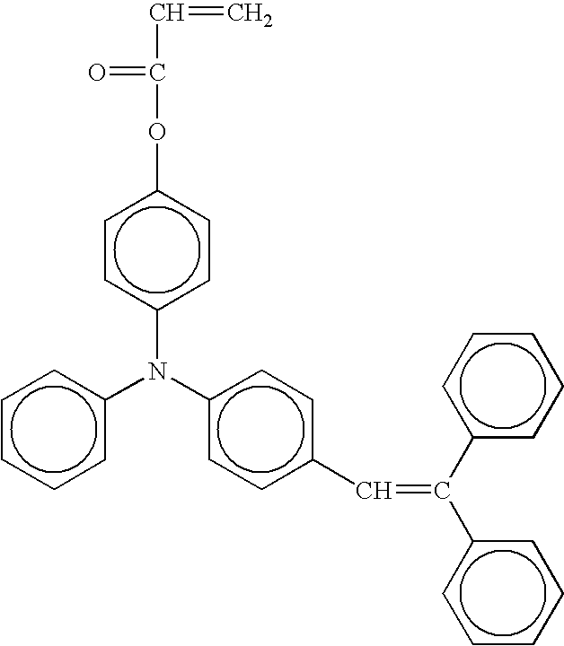
No. 46 
No. 47 
No. 48 
-
TABLE 1-4 No. 49 
No. 50 
No. 51 
No. 52 
No. 53 
No. 54 
No. 55 
No. 56 
No. 57 
No. 58 
No. 59 
No. 60 
-
TABLE 1-5 No. 61 
No. 62 
No. 63 
No. 64 
No. 65 
No. 66 
No. 67 
No. 68 
No. 69 
No. 70 
No. 71 
No. 72 
-
TABLE 1-6 No. 73 
No. 74 
No. 75 
No. 76 
No. 77 
No. 78 
No. 79 
No. 80 
No. 81 
No. 82 
No. 83 
No. 84 
No. 85 
No. 86 
No. 87 
No. 88 
-
TABLE 1-7 No. 89 
No. 90 
No. 91 
No. 92 
No. 93 
No. 94 
No. 95 
No. 96 
No. 97 
No. 98 
No. 99 
No. 100 
-
TABLE 1-8 No. 101 
No. 102 
No. 103 
No. 104 
No. 105 
No. 106 
No. 107 
No. 108 
No. 109 
No. 110 
No. 111 
No. 112 
-
TABLE 1-9 No. 113 
No. 114 
No. 115 
No. 116 
No. 117 
No. 118 
No. 119 
No. 120 
No. 121 
No. 122 
No. 123 
No. 124 
-
TABLE 1-10 No. 125 
No. 126 
No. 127 
No. 128 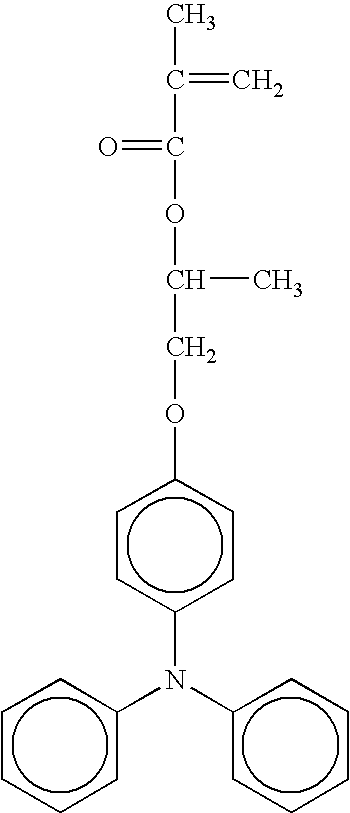
No. 129 
No. 130 
No. 131 
No. 132 
No. 133 
No. 134 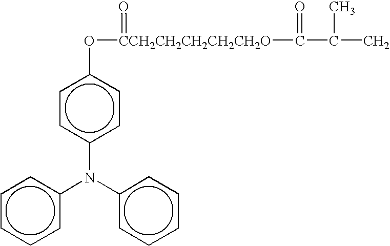
No. 135 
No. 136 
-
TABLE 1-11 No. 137 
No. 138 
No. 139 
No. 140 
No. 141 
No. 142 
No. 143 
No. 144 
No. 145 
No. 146 
No. 147 
No. 148 
No. 149 
-
TABLE 1-12 No. 150 
No. 151 
No. 152 
No. 153 
No. 154 
No. 155 
No. 156 
No. 157 
No. 158 
No. 159 
No. 160 
- The radical polymerizing compound having one functional group with a charge transporting structure for use in the present invention is essential for imparting a charge transportability to the crosslinked surface layer, and is preferably included therein in an mount of 20 to 80% by weight, and more preferably from 30 to 70% by weight based on total weight. When less than 20% by weight, the crosslinked surface layer cannot maintain the charge transportability and the sensitivity of the resultant photoreceptor deteriorates resulting in residual potential increases by repeated use. When greater than 80% by weight, the content of the monomer having three or more functional groups without a charge transporting structure decreases and the crosslinked density deteriorates Therefore, the resultant photoreceptor does not have a high abrasion resistance. In consideration of a balance between required abrasion resistance and electrical properties, the content of the radical polymerizing compound having one functional group with a charge transporting structure is preferably from 30 to 70% by weight.
- Specific examples of the reactive silicone compound having a radical polymerizing functional group and a dimethyl siloxane structure as a repeat unit include a compound having at least one radical polymerizing fuinctional group and a dimethyl siloxane structure as a repeat unit. Specific examples of the radical polymerizing functional group include those used in the radical polymerizing monomer having three or more functional groups without a charge transporting structure, and particularly an acryloyloxy group and a methacryloyloxy group are used.
- Further, in terms of hardening speed and solubility, the acryloyloxy group is more preferably used. The acryloyloxy group having two or more functional groups provide more desirable results than that having one functional group, and the acryloyloxy group having diacrylate at both ends is preferable. The reactive silicone compound optimally has a molecular weight not greater than 20,000, and ideally not greater than 10,000. When greater than 20,000, the solubility with the radical polymerizing monomer having three or more functional groups without a charge transporting structure and radical polymerizing compound having one functional group with a charge transporting structure deteriorates Therefore, the surface smoothness of the crosslinked surface layer deteriorates.
- Further, the reactive silicone compound preferably has a viscosity not greater than 30 Pa.s, and more preferably not greater than 20 Pa.s at 25° C. When greater than 30 Pa.s, a surface layer coating liquid has a high viscosity if a large amount of the reactive silicone compound isused. Therefore, it becomes difficult to coat the coating liquid, and the coated layer has defects such as pin holes and small foamed bubbles resulting in deterioration of smoothness.
- In the present invention, the viscosity is measured by rotary viscometer TV-20 from TOKIMEC INC. in a constant temperature tank under conditions of 1.0 rpm at 25° C. However, any devices can be used provided the devices have similar performance to TV-20.
- Specific examples of the silicone compound having a radical polymerizing functional group include a compound including one radical polymerizing functional group and another compound including two radical polymerizing functional groups, and having the following formulae (4) and (5) respectively:

- In compound (4), R41 represents a radical polymerizing functional group used in the radical polymerizing monomer having three or more functional groups without a charge transporting structure such as an acryloyloxy group and a methacryloyloxy group; R42, R43, R44, R45 and R46 independently represent a hydrogen atom, or an alkyl group or an aryl group having 1 to 12 carbon atoms; A represents an alkylene group having 2 to 6 carbon atoms or a single bond; and n represents an integer not less than 2.

- In the compound above (5), R41 and R46 represent a radical polymerizing functional group used in the radical polymerizing monomer having three or more functional groups without a charge transporting structure such as an acryloyloxy group and a methacryloyloxy group; R42, R43, R44, R45 and R45 independently represent a hydrogen atom, or an alkyl group or an aryl group having 1 to 12 carbon atoms; A represents an alkylene group having 2 to 6 carbon atoms or a single bond; and n represents an integer not less than 2.
- In the formulae (4) and (5), the radical polymerizing functional group is located at the end of the polysiloxane structure. However, a location of the radical polymerizing functional group of the reactive silicone compound having a radical polymerizing functional group and a dimethyl siloxane structure as a repeat unit for use in the present invention is not limited thereto, and a reactive silicone compound having a radical polymerizing functional group and a dimethyl siloxane structure as a repeat unit substituting a side chain of the polysiloxane structure can also be effectively used.
- The reactive silicone compound having a radical polymerizing functional group and a dimethyl siloxane structure as a repeat unit of the present invention can be formed by a method of performing a condensed reaction between an ester formed of an acrylic or a methacrylic acid and alkylene glycol and a trimethylsilyl compound or a polydimethylsiloxane compound, or a method of performing a condensed reaction between an ester formed of an acrylic or a methacrylic acid and alylalcohol and a trimethylsilyl compound or a polydimethylsiloxane compound, a currently available product can also be used.
- Specific examples of available products include X-22-164A having a molecular weight of 860, X-22-164B having a molecular weight of 1,630, X-22-164C having a molecular weight of 2,370, X-22-174DX having a molecular weight of 4,600, X-24-8201 having a molecular weight of 2,100 and X-22-2426 having a molecular weight of 12,000 from Shin-Etsu Chemical Co., Ltd.; bi-terminal Silaplane FM-7711 having a molecular weight of 1,000, bi-terminal Silaplane FM-7721 having a molecular weight of 5,000, bi-terminal Silaplane FM-7725 having a molecular weight of 10,000, mono-terminal Silaplane FM-0711 having a molecular weight of 1,000, mono-terminal Silaplane FM-0721 having a molecular weight of 5,000, mono-terminal Silaplane FM-0725 having a molecular weight of 10,000, mono-terminal Silaplane TM-0701 having a molecular weight of 423, and mono-terminal Silaplane TM-0701T having a molecular weight of 423 from CHISSO CORPORATION; BYK-UV3500, BYK-UV3510 and BYK-UV3570 from BYK Chemie Japan K.K.; and TEGO Rad 2100, TEGO Rad 2200N, TEGO Rad 2250, TEGO Rad 2500, TEGO Rad 2600 and TEGO Rad 2700 from Tego Chemie Service GmbH, and these are not limited thereto.
- The reactive silicone compound can be used alone or in combination. A content of the reactive silicone compound is from 0.01 to 30% by weight, and more preferably from 0.05 to 20% by weight based on total weight of solid content in a coating liquid forming the crosslinked surface layer. When less than 0.01% by weight, the crosslinked surface layer includes not enough lubricant to have sufficient low surface energy and good cleanability. When greater than 30% by weight, an amount of the lubricant is so large that an unreacted molecule, which is not chemically taken in a matrix of the crosslinked surface layer, appears and causes variations of electrical properties of the resultant photoreceptor. Thus resulting in deterioration of image density and thin characters. Although it depends on a required abrasion resistance and electrical properties, a content of the reactive silicone compound having a radical polymerizing functional group is most preferably from 0.05 to 20% by weight based on total weight of the solid content in the coating liquid forming the crosslinked surface layer.
- The surface layer of the present invention is a crosslinked surface layer wherein at least the radical polymerizing monomer having three or more functional groups without a charge transporting structure, the radical polymerizing compound having one functional group with a charge transporting structure, and the reactive silicone compound having a radical polymerizing functional group are hardened at the same time. The surface layer can also include a particulate filler to improve abrasion resistance.
- Specific examples of organic filler materials include fluorocarbon resin powders such as polytetrafluoroethylene, a silicone resin powder and an A-carbon powder. Specific examples of inorganic filler materials include metallic powders such as copper, tin, aluminium and indium; metallic oxides such as a silicon oxide, an aluminium oxide, a tin oxide, a zinc oxide, a titanium oxide, an indium oxide, an antimony oxide and a bismuth oxide; and kalium titanate. The inorganic filler material is advantageously used in terms of hardness of the filler. Particularly silicon oxide, aluminium oxide and titanium oxide are more effectively used. In addition, colloidal silica and colloidal alumina are also suitable replacements.
- The filler preferably has a primary particle diameter of from 0.01 to 0.5 μm in terms of a light transmittance and an abrasion resistance of the surface layer. When less than 0.01 μm, dispersibility deteriorates and the surface does not have a sufficient abrasion resistance. When greater than 0.5 μm, the filler quickly settles down in a dispersion liquid and filming of a toner over the surface layer occurs.
- The higher the concentration of the filler material in the surface layer, the higher the abrasion resistance. However, when the concentration is too high, a residual potential increases and the writing light transmittance of the surface layer deteriorates. Therefore, the filler material preferably has a concentration not greater than 50% by weight, and optimally not greater than 30% by weight based on total weight of solid contents in the surface layer.
- Further, a surface of the filler is preferably treated with a surface treatment agent to improve dispersibility. The dispersibility deterioration of the filler causes an increase of a residual potential and transparency deterioration of the surface layer and a defect thereof, as well as further deterioration of abrasion resistance.
- Specific examples of the surface treatment agent used to include titanate coupling agents, aluminium coupling agents, zircoaluminate coupling agents, higher fatty acids and mixtures of each agent with a silane coupling agents; and AL2O3, TiO2, ZRO2, silicone, aluminium stearate and their mixtures. These are used to improve dispersibility of the filler and prevent blurred images. The silane coupling agents occasionally cause blurred images, but a mixture of the surface treatment agent and the silane coupling agent can prevent the influence. Although an amount of the surface treatment agent depends on the primary particle diameter of a filler, the amount is preferably from 3 to 30% by weight, and optimally from 5 to 20% by weight base on total weight of the filler. When less than 3% by weight, the filler is not well dispersed. When greater than 30% by weight, the residual potential significantly increases. These filler materials can be used alone or in combination.
- The surface layer of the present invention is a crosslinked surface layer wherein at least the radical polymerizing monomer having three or more functional groups without a charge transporting structure, the radical polymerizing compound having one functional group with a charge transporting structure, and the reactive silicone compound having a radical polymerizing functional group are hardened at the same time. The surface layer can also include a radical polymerizing monomer and a radical polymerizing oligomer having one or two functional groups to control a viscosity of the surface layer when coated, reduce stress, impart a low surface free energy and reduce friction coefficient thereof. Known radical polymerizing monomers and oligomers can be used.
- Specific examples of the radical monomer having one functional group include 2-ethylhexylacrylate, 2-hydroxyethylacrylate, 2-hydroxypropylacrylate, tetrahydrofurfurylacrylate, 2-ethylhexylcarbitolacrylate, 3-methoxybutylacrylate, benzylacrylate, cyclohexylacrylate, isoamylacrylate, isobutylacrylate, methoxytriethyleneglycolacrylate, phenoxytetraethyleneglycolacrylate, cetylacrylate, isostearylacrylate, stearylacrylate, styrene monomer, etc.
- Specific examples of the radical monomer having two functional groups include 1,3-butanediolacrylate, 1,4-butanedioldiacrylate, 1,4-butanedioldimethacrylate, 1,6-hexanedioldiacrylate, 1,6-hexanedioldimethacrylate, diethyleneglycoldiacrylate, neopentylglycoldiacrylate, EO-modified bisphenol A diacrylate, EO-modified bisphenol F diacrylate, etc.
- Specific examples of the functional monomers include octafluoropentylacrylate, 2-perfluorooctylethylacrylate, 2-perfluorooctylethylmethacrylate, 2-perfluoroisononylethylacrylate, etc. wherein a fluorine atom is substituted.
- Specific examples of the radical polymerizing oligomer includes epoxyacrylate oligomers, urethaneacrylate oligomers and polyetseracrylate oligomers.
- However, when the crosslinked surface layer includes a large amount of the radical polymerizing monomer and radical polymerizing oligomer having one or two functional groups, the three-dimensional crosslinked bonding density substantially deteriorates, resulting in deterioration of abrasion resistance. Therefore, the surface layer of the present invention preferably includes the monomers and oligomers in an amount not greater than 50 parts by weight, and not greater than 30 parts by weight per 100 parts by weight of the radical polymerizing monomer having three or more functional groups.
- The surface layer of the present invention is a crosslinked surface layer wherein at least the radical polymerizing monomer having three or more functional groups without a charge transporting structure, the radical polymerizing compound having one functional group with a charge transporting structure, and the reactive silicone compound having a radical polymerizing functional group are hardened at the same time. The layer can optionally include a polymerization initiator to effectively proceed the crosslinking reaction.
- Specific examples of the heat polymerization initiators include peroxide initiators such as 2,5-dimethylhexane-2,5-dihydrooxide, dicumylperoxide, benzoylperoxide, t-butylcumylperoxide, 2,5-dimethyl-2,5-di(peroxybenzoyl)hexyne-3, di-t-butylbeloxide, t-butylhydrobeloxide, cumenehydobeloxide and lauroylperoxide; and azo initiators such as azobisisobutylnitrile, azobiscyclohexanecarbonitrile, azobisisomethylbutyrate, azobisisobutylamidinehydorchloride and 4,4′-azobis-4-cyanovaleric acid.
- Specific examples of the photo polymerization initiators include acetone or ketal photo polymerization initiators such as diethoxyacetophenone, 2,2-dimethoxy-1,2-diphenylethane-1-one, 1-hydroxy-cyclohexyl-phenyl-ketone, 4-(2-hydroxyethoxy)phenyl-(2-hydroxy-2-propyl)ketone, 2-benzyl-2-dimethylamino-1-(4-molpholinophenyl)butanone-1,2-hydroxy-2-methyl-1-phenylpropane-1-one and 1-phenyl-1,2-propanedion-2-(o-ethoxycarbonyl)oxime; benzoinether photo polymerization initiators such as benzoin, benzoinnethylether, benzoinethylether, benzoinisobutylether and benzoinisopropylether; benzophenone photo polymerization initiators such as benzophenone, 4-hydroxybenzophenone, o-benzoylmethylbenzoate, 2-benzoylnaphthalene, 4-benzoylviphenyl, 4-benzoylphenylether, acrylated benzophenone and 1,4-benzoylbenzene; thioxanthone photo polymerization initiators such as 2-isopropylthioxanthone, 2-chlorothioxanthone, 2,4-dimethylthioxanthone, 2,4-diethylthioxanthone and 2,4-dichlorothioxanthone; and other photo polymerization initiators such as ethylanthraquinone, 2,4,6-trimethylbenzoyldiphenylphosphineoxide, 2,4,6-trimethylbenzoyldiphenylethoxyphosphineoxide, bis(2,4,6-trimethylbenzoyl)phenylphosphineoxide, bis(2,4-dimethoxybenzoyl)-2,4,4-trimethylpentylphosphineoxide, methylphenylglyoxyester, 9,10-phenanthrene, acridine compounds, triazine compounds and imidazole compounds.
- Further, a material having a photo polymerizing effect can be used alone or in combination with the above-mentioned photo polymerization initiators. Specific examples of the materials include triethanolamine, methyldiethanol amine, 4-dimethylaminoethylbenzoate, 4-imethylaminoisoamylbenzoate, ethyl(2-dimethylamino)benzoate and 4,4-dimethylaminobenzophenone.
- These polymerization initiators can be used alone or in combination. The surface layer of the present invention preferably includes the polymerization initiators in an amount of 0.5 to 40 parts by weight, and optimally from 1 to 20 parts by weight per 100 parts by weight of the radical polymerizing compounds.
- Further, a coating liquid for the surface layer of the present invention may include various additives such as plasticizers (to soften stress and improve adhesiveness thereof), leveling agents and low-molecular-weight charge transport materials without radical reactivity. Known additives can be used, and specific examples of the plasticizers include plasticizers such as dibutylphthalate and dioctylphthalate. The content is preferably not greater than 20% by weight, and optimally not greater than 10% based on total weight of solid contents of the coating liquid. Specific examples of the leveling agents include silicone oil such as dimethylsilicone oil and methylphenylsilicone oil; and polymers and oligomers having a perfluoroalkyl group in the side chain. The content thereof is preferably not greater than 3% by weight.
- The coating liquid for the surface layer of the present invention can include a binder resin. However, the coating liquid is provided only if smoothness, electrical properties or durability of a surface of the photoreceptor is not impaired.
- However, when a polymer material such as a binder resin is included in the coating liquid, the binder resin is insoluble with a polymer produced by a hardening reaction of the radical polymerizing compositions (the radical polymerizing monomer and the radical polymerizing compound having a charge transporting structure). Thus, phase separation appears resulting in large concavities and convexities of the crosslinked surface layer. Therefore, it is preferable not to use the binder resin.
- The crosslinked surface layer of the present invention is formed by coating and hardening a coating liquid including at least the radical polymerizing monomer having three or more functional groups without a charge transporting structure, the radical polymerizing compound having one functional group with a charge transporting structure, and the reactive silicone compound having a radical polymerizing fuinctional group. The coating liquid can include other components when the radical polymerizing monomer is a liquid, and is optionally diluted with a solvent and coated.
- Specific examples of the solvent include alcohols such as methanol, ethanol, propanol and butanol; ketones such as acetone, methyl ethyl ketone, methyl isobutyl ketone and cyclohexanone; esters such as ethyl acetate and butyl acetate; ethers such as tetrahydrofuran, dioxane and propylether; halogens such as dichloromethane, dichloroethane, trichloroethane and chlorobenzene; aromatics such as benzene, toluene and xylene; and Cellosoves such as methyl Cellosolve, ethyl Cellosolve and Cellosolve acetate.
- These solvents can be used alone or in combination. A dilution ratio with the solvent can be selected based on solubility of the compositions, coating method and layer thickness. The crosslinked surface layer can be coated by dip coating, spray coating, bead coating, ring coating, etc.
- In the present invention, after the coating liquid is coated to form layer, an external energy is applied for hardening the layer to form the crosslinked surface layer. The external energy includes a heat, light and radiation.
- Heat energy is applied to the layer from the coated side or from the substrate using air, a gaseous body such as nitrogen, steam, a variety of heating media, an infrared or an electromagnetic wave. The heating temperature is preferably from 100 to 170° C. When less than 100° C., the reaction is slow in speed and is not completed. When greater than 170° C., the reaction nonuniformly proceeds and large distortions appear in the crosslinked surface layer. After heated at comparatively a low temperature less than 100° C., to uniformly complete the hardening reaction the reaction is completed at not less than 100° C.
- Specific examples of the light energy include UV irradiators such as high pressure mercury lamps and metal halide lamps having an emission wavelength of UV light; and a visible light source adaptable to absorption wavelength of the radical polymerizing compounds and photo polymerization initiators. The irradiation light amount is preferably from 50 to 1,000 mW/cm2. When less than 50 mW/cm2, the hardening reaction takes an excessive amount of time. When greater than 1,000 mW/cm2, the reaction nonuniformly proceeds and the crosslinked surface layer has an excessive surface roughness. The radiation energy includes a radiation energy using an electron beam. Among these energies, the heat and light energies are preferable because of their simple reaction speed controls and simple apparatuses.
- Since the crosslinked surface layer of the present invention has a different thickness depending on the layer structure of a photoreceptor using the crosslinked surface layer, the thickness will be described according to the following explanations of the various layer structures.
- The electrophotographic photoreceptor for use in the present invention will be explained, referring to the drawings.
-
FIG. 1A andFIG. 1B are cross-sectional views of embodiments of layers of the electrophotographic photoreceptor of the present invention, which overlies an electroconductive substrate and is a single-layered photoreceptor formed of a photosensitive layer having both a charge generation function and charge transport function. InFIG. 1A , the photosensitive layer is wholly crosslinked and hardened to form a crosslinked surface layer. InFIG. 1B , a crosslinked surface layer is formed on a surface of the photosensitive layer. -
FIG. 2A andFIG. 2B are cross-sectional views of other embodiments of layers of the electrophotographic photoreceptor of the present invention, which is a multilayered photoreceptor formed of a charge generation layer having a charge generation function and a charge transport layer having a charge transport function, and which are overlying an electroconductive substrate. InFIG. 2A , the charge transport layer is wholly crosslinked and hardened to form a crosslinked surface layer. InFIG. 2B , a crosslinked surface layer is formed on a surface of the charge transport layer. - Suitable materials for use as the electroconductive substrate include materials having a volume resistance not greater than 1010 Ω·cm. Specific examples of such materials include plastic cylinders, plastic films or paper sheets. On the surface of this material is a metal such as aluminum, nickel, chromium, nichrome, copper, gold, silver, platinum and the like, or a metal oxide such as tin oxides, indium oxides and the like. The metallic layer is deposited or sputtered. In addition, a plate of a metal such as aluminum, aluminum alloys, nickel and stainless steel and a metal cylinder, can also be used as the substrate. The plate of metal is prepared by tubing a metal such as the metals mentioned above by a method such as impact ironing or direct ironing, and then treating the surface of the tube by cutting, super finishing, polishing and the like treatments, can also be used as the substrate. Further, endless belts of a metal such as nickel and stainless steel, which have been disclosed in Japanese Laid-Open Patent Publication No. 52-36016, can also be used as the substrate.
- Furthermore, substrates, in which a coating liquid including a binder resin and an electroconductive powder is coated on the supporters mentioned above, can be used as the substrate.
- Specific examples of such an electroconductive powder include carbon black, acetylene black, powders of metals such as aluminum, nickel, iron, Nichrome, copper, zinc, silver and the like, and metal oxides such as electroconductive tin oxides, ITO and the like. Specific examples of the binder resin include known thermoplastic resins, thermosetting resins and photo-crosslinking resins, such as polystyrene, styrene-acrylonitrile copolymers, styrene-butadiene copolymers, styrene-maleic anhydride copolymers, polyesters, polyvinyl chloride, vinyl chloride-vinyl acetate copolymers, polyvinyl acetate, polyvinylidene chloride, polyarylates, phenoxy resins, polycarbonates, cellulose acetate resins, ethyl cellulose resins, polyvinyl butyral resins, polyvinyl formal resins, polyvinyl toluene, poly-N-vinyl carbazole, acrylic resins, silicone resins, epoxy resins, melamine resins, urethane resins, phenolic resins, alkyd resins and the like resins.
- Such an electroconductive layer can be formed by coating a liquid in which an electroconductive powder and a binder resin are dispersed in a solvent such as tetrahydrofuran, dichloromethane, methyl ethyl ketone, toluene and the like solvent, and then drying the coated liquid.
- In addition, substrates, in which an electroconductive resin film is formed on a surface of a cylindrical substrate using a heat-shrinkable resin tube made of a combination of a resin such as polyvinyl chloride, polypropylene, polyesters, polyvinylidene chloride, polyethylene, chlorinated rubber and fluorine-containing resins, with an electroconductive material, can also be used as the substrate.
- Next, the photosensitive layer will be described. The photosensitive layer may be a single-layered or a multilayered. The multilayered photosensitive layer is formed of a charge generation layer having a charge generation function and a charge transport layer having a charge transport function. The single-layered photosensitive layer is a layer having both the charge generation function and charge transport function.
- Hereinafter, the multilayered photosensitive layer and single-layered photosensitive layer will be explained respectively.
- The charge transport layer (CGL) is mainly formed of a charge generation material, and optionally includes a binder resin. Suitable charge generation materials include inorganic materials and organic materials.
- Specific examples of the inorganic charge generation materials include crystalline selenium, amorphous selenium, selenium-tellurium alloys, selenium-tellurium-halogen alloys and selenium-arsenic alloys.
- Specific examples of the organic charge generation materials include known materials, for example, phthalocyanine pigments such as metal phthalocyanine and metal-free phthalocyanine, azulenium pigments, squaric acid methine pigments, azo pigments having a carbazole skeleton, azo pigments having a triphenylamine skeleton, azo pigments having a diphenylamine skeleton, azo pigments having a dibenzothiophene skeleton, azo pigments having a fluorenone skeleton, azo pigments having an oxadiazole skeleton, azo pigments having a bisstilbene skeleton, azo pigments having a distyryloxadiazole skeleton, azo pigments having a distyrylcarbazole skeleton, perylene pigments, anthraquinone pigments, polycyclic quinone pigments, quinoneimine pigments, diphenyl methane pigments, triphenyl methane pigments, benzoquinone pigments, naphthoquinone pigments, cyanine pigments, azomethine pigments, indigoid pigments, bisbenzimidazole pigments and the like materials. These charge transport materials can be used alone or in combination.
- Specific examples of the binder resin optionally used in the CGL include polyamide resins, polyurethane resins, epoxy resins, polyketone resins, polycarbonate resins, silicone resins, acrylic resins, polyvinyl butyral resins, polyvinyl formal resins, polyvinyl ketone resins, polystyrene resins, poly-N-vinylcarbazole resins, polyacrylamide resins, and the like resins. These resins can be used alone or in combination.
- In addition, a charge transport polymer material aside from the above-mentioned binder resins can also be used in the CGL. Specific examples include polymer materials such as polycarbonate resins, polyester resins, polyurethane resins, polyether resins, polysiloxane resins and acrylic resins having an arylamine skeleton, a benzidine skeleton, a hydrazone skeleton, a carbazole skeleton, a stilbene skeleton, a pyrazoline skeleton, etc.; and polymer materials having polysilane skeleton.
- Specific examples of the former polymer materials include charge transport polymer materials disclosed in Japanese Laid-Open Patent Publications Nos. 01-001728, 01-009964, 01-013061, 01-019049, 01-241559, 04-011627, 04-175337, 04-183719, 04-225014, 04-230767, 04-320420, 05-232727, 05-310904, 06-234838, 06-234839, 06-234840, 06-234839, 06-234840, 06-234841, 06-236051, 06-295077, 07-056374, 08-176293, 08-208820, 08-211640, 08-253568, 08-269183, 09-062019, 09-043883, 09-71642, 09-87376, 09-104746, 09-110974, 09-110976, 09-157378, 09-221544, 09-227669, 09-235367, 09-241369, 09-268226, 09-272735, 09-302084, 09-302085, 09-328539, etc.
- Specific examples of the latter polymer materials include polysilylene polymers disclosed in Japanese Laid-Open Patent Publications Nos. 63-285552, 05-19497, 05-70595, 10-73944, etc.
- The CGL also can include a low-molecular-weight charge transport material.
- The low-molecular-weight charge transport materials include positive hole transport materials and electron transport materials.
- Specific examples of the electron transport materials include electron accepting materials such as chloranil, bromanil, tetracyanoethylene, tetracyanoquinodimethane, 2,4,7-trinitro-9-fluorenone, 2,4,5,7-tetranitro-9-fluorenone, 2,4,5,7-tetranitro-xanthone, 2,4,8-trinitrothioxanthone, 2,6,8-trinitro-4H-indeno[1,2-b]thiophene-4-one, 1,3,7-trinitrobenzothiophene-5,5-dioxide, diphenoquinone derivatives, etc. These electron transport materials can be used alone or in combination.
- Specific examples of the positive hole transport materials include electron donating materials such as oxazole derivatives, oxadiazole derivatives, imidazole derivatives, monoarylamines derivatives, diarylamine derivatives, triarylamine derivatives, stilbene derivatives, α-phenylstilbene derivatives, benzidine derivatives, diarylmethane derivatives, triarylmethane derivatives, 9-styrylanthracene derivatives, pyrazoline derivatives, divinylbenzene derivatives, hydrazone derivatives, indene derivatives, butadiene derivatives, pyrene derivatives, bisstilbene derivatives, enamine derivatives, and other known materials. These positive hole transport materials can be used alone or in combination.
- Suitable methods for forming the charge generation layer are classified into vacuum thin film forming method and solvent dispersion casting method.
- Specific examples of the former vacuum thin film forming method include a vacuum evaporation method, a glow discharge decomposition method, an ion plating method, a sputtering method, a reaction sputtering method, CVD (chemical vapor deposition) methods, etc. A layer of the above-mentioned inorganic and organic materials can be formed by the above methods.
- The casting method for forming the charge generation layer typically includes the following steps:
-
- (1) preparing a coating liquid by mixing one or more inorganic or organic charge generation materials mentioned above with a solvent such as tetrahydrofuran, dioxane, dioxolan, toluene, dichloromethane, monochlorobenzene, dichloroethane, cyclohexanone, cyclopentanone, anisole, xylene, methyl ethyl ketone, acetone, ethyl acetate, butyl acetate, etc., optionally with a binder resin and a leveling agent such as a dimethylsilicone oil and methylphenyl silicone oil. Then dispersing the materials with a ball mill, an attritor, a sand mill, beads mill, etc. to prepare a CGL coating liquid;
- (2) coating the CGL coating liquid, which is diluted if necessary, on a substrate by a method such as dip coating, spray coating, bead coating and ring coating; and
- (3) drying the coated liquid to form a CGL.
- The thickness of the CGL is preferably from about 0.01 to about 5 μm, and optimally from about 0.05 to about 2 μm.
- The charge transport layer (CTL) is a layer having a charge transportability, and the crosslinked surface layer of the present invention is effectively used as a CTL. After a coating liquid including the radical polymerizing monomer having three or more functional groups without a charge transporting structure; radical polymerizing compound having one functional group with a charge transporting structure; and reactive silicone compound having a radical polymerizing functional group (hereinafter referred to as the radical polymerizing compositions) is coated on the CGL and is optionally dried to form a coated layer thereon, an external energy is applied thereto to harden the coated layer to form the crosslinked surface layer. The crosslinked surface layer preferably has a thickness of from 10 to 30 μm, and optimally from 10 to 25 μm. When thinner than 10 μm, a sufficient charged potential cannot be maintained. When thicker than 30 μm, a contraction in volume when hardened tends to cause separation from a lower layer.
- When the crosslinked surface layer is formed on a surface of the CTL, the CTL is formed by coating a CGL with a coating liquid wherein a charge transport material having a charge transportability and a binder resin are dispersed in a proper solvent to form a coated layer is dried. The crosslinked surface layer is formed by coating the CGL with a coating liquid including the above-mentioned radical polymerizing compositions of the present invention to form a coated layer thereon, and crosslinking and hardening the coated layer with an external energy.
- Specific examples of charge transport materials include electron transport materials, positive hole transport materials and charge transport polymer materials used in the CGL. Particularly, the charge transport polymer materials are used to reduce a solution of a lower layer when a surface layer is coated thereon.
- Specific examples of the binder resins include thermoplastic or thermosetting resins such as polystyrene, styrene-acrylonitrile copolymers, styrene-butadiene copolymers, styrene-maleic anhydride copolymers, polyester, polyvinylchloride, vinylchloride-vinylacetate copolymers, polyvinylacetate, polyvinylidenechloride, polyarylate resins, phenoxy resins, polycarbonate, cellulose acetate resins, ethylcellulose resins, polyvinylbutyral, polyvinylformal, polyvinyltoluene, poly-N-vinylcarbazole, acrylic resins, silicone resins, epoxy resins, melamine resins, urethane resins, phenol resins and alkyd resins.
- The CTL preferably includes the charge transport material in an amount of from 20 to 300 parts by weight, and optimally from 40 to 150 parts by weight per 100 parts by weight of the binder resin. However, the charge transport polymer material can be used alone or in combination with the binder resin.
- Specific examples of the solvent used for coating the CTL include the solvents previously discussed used for coating the CGL, and particularly the solvents optimizing the charge transport material and binder resin. These solvents can be used alone or in combination. The CTL can be formed by the same coating methods used for coating the CGL.
- The CTL may optionally include a plasticizer and a leveling agent.
- Specific examples of the plasticizers include plasticizers for typical resins, such as dibutylphthalate and dioctylphthalate, and a content thereof is preferably from 0 to 30 parts by weight per 100 parts by weight of the binder resin.
- Specific examples of the leveling agents include silicone oil such as dimethyl silicone oil and methylphenyl silicone oil; and polymers or oligomers having a perfluoroalkyl group in the side chain, and a content thereof is preferably from 0 to 1 part by weight per 100 parts by weight of the binder resin.
- The CTL preferably has a thickness of from 5 to 40 μm, and optimally from 10 to 30 μm.
- When the crosslinked surface layer overlies the CTL, as mentioned in the method of forming a crosslinked surface layer, a coating liquid including the radical polymerizing compositions of the present invention is coated on the CTL and optionally dried to form a coated layer. An external energy is then applied to harden the coated layer to form the crosslinked surface layer. The crosslinked surface layer preferably has a thickness of from 1 to 20 μm, and optimally from 2 to 10 μm. When thinner than 1 μm, uneven thickness causes uneven durability. When thicker than 20 μm, a total thickness of the CTL and crosslinked surface layer is so thick that charges are scattered, resulting in deterioration of image reproducibility of the resultant photoreceptor.
- The single-layered photosensitive layer has both a charge generation function and a charge transport function. The crosslinked surface layer has a charge transporting structure including a charge generation material with a charge generating function of the present invention and is effectively used as a single-layered photosensitive layer. As mentioned in the casting method of forming the CGL, a charge generation material is dispersed in a coating liquid including the radical polymerizing compositions, and the coating liquid is coated on an electroconductive substrate and dried to form a coated layer. Then a hardening reaction is performed in the coated layer with an external energy to form the crosslinked surface layer. The charge generation material may previously be dispersed in a solvent to prepare a dispersion, and the dispersion may be added into the coating liquid for forming the crosslinked surface layer. The crosslinked surface layer preferably has a thickness of from 10 to 30 μm, and optimally from 10 to 25 μm. When thinner than 10 μm, a sufficient charged potential cannot be maintained. When thicker than 30 μm, a contraction in volume when hardened causes separation from an undercoat layer.
- When the crosslinked surface layer overlies a single-layered photosensitive layer, the photosensitive layer can be formed by coating and drying a liquid wherein a charge generation material having a charge generation function, a charge transport material having a charge transport function and a binder resin are dispersed or dissolved in a proper solvent. The photosensitive layer may optionally include an additive such as plasticizers and leveling agents. The methods of dispersing a charge generation material, charge generation materials, charge transport materials, plasticizers and leveling agents mentioned in the above CGL and CTL can be used. Besides the binder resins mentioned in the above CTL, the binder resins in the above CGL can be mixed. In addition, the above-mentioned charge transport polymer material can effectively be used to prevent components of the lower photosensitive layer from mixing in the crosslinked surface layer. The photosensitive layer preferably has a thickness of from 5 to 30 μm, and optimally from 10 to 25 μm.
- When the crosslinked surface layer overlies a single-layered photosensitive layer, as mentioned in the method of forming a crosslinked surface layer, a coating liquid including the radical polymerizing compositions of the present invention and a binder resin are coated on the photosensitive layer and optionally dried to form a coated layer. An external energy is then applied to harden the coated layer to form the crosslinked surface layer. The crosslinked surface layer preferably has a thickness of from 1 to 20 μm, and optimally from 2 to 10 μm. When thinner than 1 μm, uneven thickness causes uneven durability.
- The single-layered photosensitive layer preferably includes a charge generation material in an amount of from 1 to 30% by weight, a binder resin of from 20 to 80% by weight and a charge transport material of from 10 to 70 parts by weight based on total weight of the layer.
- The photoreceptor of the present invention can have an intermediate layer between a crosslinked surface layer and a photosensitive layer when the crosslinked surface layer overlies the intermediate layer. The intermediate layer prevents components of the lower photosensitive layer from mixing in the crosslinked surface layer and avoids inhibition in the hardening reaction and concavities and convexities that occur as a result. In addition, the intermediate layer can improve an adhesiveness between the crosslinked surface layer and photosensitive layer.
- The intermediate layer includes a resin as a main component. Specific examples of the resin include polyamides, alcohol-soluble nylons, water-soluble polyvinyl butyral, polyvinyl butyral, polyvinyl alcohol, etc. The intermediate layer can be formed by one of the above-mentioned known coating methods. The intermediate layer preferably has a thickness of from 0.05 to 2 μm.
- The photoreceptor of the present invention may have an undercoat between the substrate and photosensitive layer. The undercoat layer includes a resin as a main component. Since a photosensitive layer is typically formed on the undercoat layer by coating a liquid including an organic solvent, this resin in the undercoat layer has good resistance to general organic solvents. Specific examples of such resins include water-soluble resins such as polyvinyl alcohol resins, casein and polyacrylic acid sodium salts; alcohol soluble resins such as nylon copolymers and methoxymethylated nylon resins; and thermosetting resins capable of forming a three-dimensional network such as polyurethane resins, melamine resins, alkyd-melamine resins, epoxy resins and the like. The undercoat layer may include a fine powder of metal oxides such as titanium oxide, silica, alumina, zirconium oxide, tin oxide and indium oxide to prevent occurrence of moire in the recorded images and to decrease residual potential of the photoreceptor.
- The undercoat layer can also be formed by coating a coating liquid using a proper solvent and a proper coating method similarly to those used in the formation of the photosensitive layer mentioned above. The undercoat layer may be formed using a silane coupling agent, titanium coupling agent or a chromium coupling agent. In addition, a layer of aluminum oxide, which is formed by an anodic oxidation method, and a layer of an organic compound such as polyparaxylylene (parylene) or an inorganic compound such as SiO, SnO2, TiO2, ITO or CeO2 which is formed by a vacuum evaporation method is also preferably used as the undercoat layer. Besides these materials, other materials can be used. The thickness of the undercoat layer is preferably from 0 to 5 μm.
- In the present invention, an antioxidant can be included in each of the layers, i.e., the crosslinked surface layer, charge generation layer, charge transport layer, undercoat layer and intermediate layer. The antioxidant is added to improve the stability to withstand environmental conditions, namely to avoid decrease of photosensitivity and increase residual potential.
- Specific examples of the antioxidant for use in the present invention include the following compound.
- (a) Phenolic Compounds
- 2,6-di-t-butyl-p-cresol, butylated hydroxyanisole, 2,6-di-t-butyl-4-ethylphenol, n-octadecyl-3-(4′-hydroxy-3′,5′-di-t-butylphenol), 2,2′-methylene-bis-(4-methyl-6-t-butylphenol), 2,2′-methylene-bis-(4-ethyl-6-t-butylphenol), 4,4′-thiobis-(3-methyl-6-t-butylphenol), 4,4′-butylidenebis-(3-methyl-6-t-butylphenol), 1,1,3-tris-(2-methyl-4-hydroxy-5-t-butylphenyl)butane, 1,3,5-trimethyl-2,4,6-tris(3,5-di-t-butyl-4-hydroxybenzyl)benzene, tetrakis-[methylene-3-(3′,5′-di-t-butyl-4′-hydroxyphenyl)propionate]methane, bis[3,3′-bis(4′-hydroxy-3′-t-butylphenyl)butyric acid]glycol ester, tocophenol compounds, etc.
- (b) Paraphenylenediamine Compounds
- N-phenyl-N′-isopropyl-p-phenylenediamine, N,N′-di-sec-butyl-p-phenylenediamine, N-phenyl-N-sec-butyl-p-phenylenediamine, N,N′-di-isopropyl-p-phenylenediamine, N,N′-dimethyl-N,N′-di-t-butyl-p-phenylenediamine, etc.
- (c) Hydroquinone Compounds
- 2,5-di-t-octylhydroquinone, 2,6-didodecylhydroquinone, 2-dodecylhydroquinone, 2-dodecyl-5-chlorohydroquinone, 2-t-octyl-5-methylhydroquinone, 2-(2-octadecenyl)-5-methylhydroquinone, etc.
- (d) Organic Sulfur-Containing Compounds
- Dilauryl-3,3′-thiodipropionate, distearyl-3,3′-thiodipropionate, ditetradecyl-3,3′-thiodipropionate, etc.
- (e) Organic Phosphorus-Containing Compounds
- Triphenylphosphine, tri(nonylphenyl)phosphine, tri(dinonylphenyl)phosphine, tricresylphosphine, tri(2,4-dibutylphenoxy)phosphine, etc.
- These compounds are known as antioxidants for rubbers, plastics, fats, etc., and can easily be obtained.
- Each of the layers preferably includes the antioxidant in an amount of 0.01 to 10% by weight based on total weight.
- Next, the image forming method and image forming apparatus of the present invention will be explained in detail, referring to the drawings.
- The image forming method and image forming apparatus of the present invention include a photoreceptor having a smooth transporting crosslinked surface layer having a low surface energy, wherein the photoreceptor is charged and irradiated with an imagewise light to form an electrostatic latent image thereon; the electrostatic latent image is developed to form a toner image; the toner image is transferred onto an image bearer (transfer sheet) and fixed thereon; and a surface of the photoreceptor is cleaned.
- The process is not limited to direct transfer of an electrostatic latent image onto a transfer sheet and development of the electrostatic latent image.
-
FIG. 3 is a schematic view illustrating a partial cross-section of an embodiment of the image forming apparatus of the present invention. A charger (3) is used to uniformly charge a photoreceptor(1). Specific examples of the charger include known chargers such as corotron devices, scorotron device, solid state chargers, needle electrode devices, roller charging devices and electroconductive brush devices. - Next, an imagewise irradiator (5) is used to form an electrostatic latent image on the photoreceptor (1). Suitable light sources include light emitters such as fluorescent lamps, tungsten lamps, halogen lamps, mercury lamps, sodium lamps, light emitting diodes (LEDs), laser diodes (LDs), light sources using electroluminescence (EL), etc. In addition, to obtain light having a desired wave length, filters such as sharp-cut filters, band pass filters, near-infrared cutting filters, dichroic filters, interference filters and color temperature converting filters can be used.
- Next, a developing unit (6) is used to visualize an electrostatic latent image formed on the photoreceptor (1). The developing methods include a one-component developing method and a two-component developing method using a dry toner; and a wet developing method using a wet toner. When the photoreceptor positively or negatively charged is exposed to imagewise light, an electrostatic latent image having a positive or negative charge is formed on the photoreceptor. When the latent image having a positive charge is developed with a toner having a negative charge, a positive image can be obtained. In contrast, when the latent image having a positive charge is developed with a toner having a positive charge, a negative image can be obtained.
- Next, a transfer charger (10) is used to transfer a toner image visualized on the photoreceptor onto a transfer sheet (9). A pre-transfer charger (7) may be used to improve this transfer process. Suitable transferers include a transferer charger, an electrostatic transferer using a bias roller, an adhesion transferer, a mechanical transferer using a pressure and a magnetic transferee. The above-mentioned chargers can be used for the electrostatic transferee.
- Next, a separation charger (11) and a separation pick (12) are used to separate the transfer sheet (9) from the photoreceptor (1). Other separation means include an electrostatic absorption induction separator, a side-edge belt separator, a tip grip conveyor, a curvature separator, etc. The above-mentioned chargers can be used for the separation charger (11).
- Next, a fur brush (14) and a cleaning blade (15) are used to remove a toner left on the photoreceptor after transfer. A pre-cleaning charger (13) may be used to perform the cleaning more effectively. Other cleaners include a web cleaner, a magnet brush cleaner, etc., and these cleaners can be used alone or in combination.
- Next, a discharger is optionally used to remove a latent image in the photoreceptor. The discharger includes a discharge lamp (2) and a discharger, and the above-mentioned light sources and chargers can be used respectively.
- Known means can be used for other an original reading process, a paper feeding process, a fixing process, a paper delivering process, etc.
- The above-mentioned image forming unit may be fixedly set in a copier, a facsimile or a printer. However, the image forming unit may be detachably set therein as a process cartridge.
FIG. 4 is a schematic view illustrating a cross-section of an embodiment of the process cartridge for the image forming apparatus of the present invention. - The process cartridge means an image forming unit (or device) which includes a photoreceptor (101) and at least one of a charger (102), an image developer (104), a transferer (106), a cleaner (107) and a discharger (not shown).
- While the photoreceptor (101) rotates in a direction indicated by an arrow, the photoreceptor (101) is charged by the charger (102) and irradiated by an irradiator (103) to form an electrostatic latent image relevant to imagewise light. The electrostatic latent image is developed by the image developer (104) with a toner to form a form a toner image, and the toner image is transferred by the transferer (106) onto a transfer sheet (105) to be printed. Next, a surface of the photoreceptor after the toner image is transferred is cleaned by the cleaner (107), discharged by a discharger (not shown) and these processes are repeated.
- As is apparent from the explanations mentioned above, the electrophotographic photoreceptor of the present invention can widely be used in electrophotography applied fields such as a laser beam printer, a CRT printer, a LED printer, a liquid crystal printer and a laser engraving.
- The compound having a charge transporting structure of the present invention is synthesized by, e.g., a method disclosed in Japanese Patent No. 3164426. The following method is such an example.
- (1) Synthesis of a Hydroxy Group Substituted Triarylamine Compound Having the Following Formula B
- 113.85 g (0.3 mol) of a methoxy group substituted triarylamine compound having the formula A, 138 g (0.92 mol) of sodium iodide and 240 ml of sulfolane were mixed to prepare a mixture. The mixture was heated to have a temperature of 60° C. in a nitrogen stream.

99 g (0.91 mol) of trimethylchlorosilane were dropped therein for 1 hr and the mixture was stirred for 4 hrs at about 60° C. About 1.5 L of toluene were added thereto and the mixture was cooled to have a room temperature, and repeatedly washed with water and an aqueous solution of sodium carbonate. Then, a solvent was removed and refined by a column chromatographic process using silica gel as an absorption medium, and toluene and ethyl acetate (20-to-1) as a developing solvent. Cyclohexane was added to the buff yellow oil to separate a crystal out. Thus, 88.1 g (yield of 80.4%) of a white crystal having the following formula B and a melting point of from 64.0 to 66.0° C. was prepared.
- (2) A Triarylamino Group Substituted Acrylate Compound
- (Compound No. 54 in Table 1)
- 82.9 g (0.227 mol) of the hydroxy group substituted triarylamine compound having the formula B prepared in (1) were dissolved in 400 ml of tetrahydrofuran to prepare a mixture. An aqueous solution of sodium hydrate formed of 12.4 g of NaOH and 100 mil of water was dropped therein in a nitrogen stream. The mixture was cooled to have a temperature of 5° C., and 25.2 g (0.272 mol) of chloride acrylate was dropped therein for 40 min. Then, the mixture was stirred at 5° C. for 3 hrs. The mixture was put in water and extracted with toluene. The extracted liquid was repeatedly washed with water and an aqueous solution of sodium carbonate. Then, a solvent was removed and refined by a column chromatographic process using silica gel as an absorption medium and toluene as a developing solvent. N-hexane was added to the colorless oil to separate a crystal. Thus, 80.73 g (yield of 84.8%) of a white crystal of the compound No. 54 having a melting point of from 117.5 to 119.0° C. was prepared.
- Having generally described this invention, further understanding can be obtained by reference to certain specific examples which are provided herein for the purpose of illustration only and are not intended to be limiting. In the descriptions in the following examples, the numbers represent weight ratios in parts, unless otherwise specified.
- An undercoat coating liquid, a charge generation coating liquid and charge transport coating liquid, which have the following formulations, were coated in this order on an aluminium cylinder by a dip coating method and dried to prepare a photoreceptor 1 having an undercoat layer of 3.5 μm thick, a CGL of 0.2 μm thick, a CTL of 23 μm thick.
Undercoat layer coating liquid Titanium dioxide powder 400 Melamine resin 65 Alkyl resin 120 2-butanone 400 CGL coating liquid Bisazo pigment having the following formula: 12 

Bisphenol Z- type Polycarbonate 5 2-butanone 200 Cyclohexanone 400 CTL coating liquid Bisphenol Z- type Polycarbonate 10 CTM having the following formula: 10 
Tetrahydrofuran 100 - The CTL was further coated with a crosslinked surface layer coating liquid having the following formulation by a spray coating method.
Crosslinked surface layer coating liquid Radical polymerizing monomer having three or more 95 functional groups without a charge transporting structure Trimethylolpropanetriacrylate (TMPTA) from TOKYO KASEI KOGYO Co., Ltd. having a molecular weight (Mw) of 296.32, 3 functional groups (Fg), and a ratio (Mw/Fg) of 99 Radical polymerizing compound having one functional 95 group with a charge transporting structure Compound No. 54 Photo polymerization initiator 10 1-hydroxy-cyclohexyl-phenyl-ketone IRGACURE 184 from CIBA SPECIALTY CHEMICALS Tetrahydrofuran 1,200 Reactive silicone compound having a radical polymerizing 10 functional group Bi-terminal methacryl-modified polysiloxane X-22-164A from Shin-Etsu Chemical Co., Ltd. having a molecular weight of 860 - The coated layer was irradiated by a metal halide lamp with an irradiation intensity of 700 mW/cm2 for 20 sec, and further dried at 130° C. for 30 min to form a crosslinked surface layer.
- Thus, an electrophotographic photoreceptor was prepared.
- The procedure for preparation of the electrophotographic photoreceptor in Example 1 was repeated to prepare an electrophotographic photoreceptor with the exception of changing the Reactive silicone compound having a radical polymerizing functional group to:
-
- Mono-terminal methacryl-modified polysiloxane X-22-174DX from Shin-Etsu Chemical Co., Ltd. having a molecular weight of 4,600, a viscosity of 60 mm2/s, a refraction index at 25° C. of 1.407, and a specific gravity at 25° C. of 0.97.
- The procedure for preparation of the electrophotographic photoreceptor in Example 1 was repeated to prepare an electrophotographic photoreceptor with the exception of changing the Reactive silicone compound having a radical polymerizing functional group to:
-
- Polydimethylsiloxane having a polyether-modified acrylic group BYK-UV3500 from BYK Chemie Japan K.K
- The procedure for preparation of the electrophotographic photoreceptor in Example 1 was repeated to prepare an electrophotographic photoreceptor with the exception of changing the Reactive silicone compound having a radical polymerizing functional group to the following one:
-
- Polydimethylsiloxane having a polyester-modified acrylic group (PO modified-2-neopenthylglycoldiacrylate) BYK-UV357 from BYK Chemie Japan K.K
- The procedure for preparation of the electrophotographic photoreceptor in Example 1 was repeated to prepare an electrophotographic photoreceptor with the exception of changing the Reactive silicone compound having a radical polymerizing functional group to the following, and the content thereof to 0.11.
-
- Crosslink reactive silicone compound polyetheracrylate TEGO Rad 2200N from Tego Chemie Service GmbH
- The procedure for preparation of the electrophotographic photoreceptor in Example 1 was repeated to prepare an electrophotographic photoreceptor with the exception of changing the Reactive silicone compound having a radical polymerizing functional group to the following, and the content thereof to 50.
- Bi-terminal Silaplane FM-7721 having a molecular weight of 5,000 from CHISSO CORPORATION
- The procedure for preparation of the electrophotographic photoreceptor in Example 1 was repeated to prepare an electrophotographic photoreceptor with the exception of changing the radical polymerizing monomer having three or more functional groups without a charge transporting structure to:
-
- Pentaerythritoltetraacrylate SR-295 having a molecular weight (Mw)of 352.34, four function groups (Fg), and a ratio (Mw/Fg) of 88 from Sartomer Company, Inc.
- The procedure for preparation of the electrophotographic photoreceptor in Example 1 was repeated to prepare an electrophotographic photoreceptor with the exception of changing the radical polymerizing monomer having three or more functional groups without a charge transporting structure to:
-
- Dipentaerythritolhexaacrylate KAYARAD DPHA having a molecular weight (Mw) of 551.55, 5.5 function groups (Fg), and a ratio (Mw/Fg) of 100 from Nippon Kayaku Co., Ltd.
- The procedure for preparation of the electrophotographic photoreceptor in Example 1 was repeated to prepare an electrophotographic photoreceptor with the exception of changing the radical polymerizing monomer having three or more functional groups without a charge transporting structure to:
-
- Caprolactone-modified dipentaerythritolhexaacrylate KAYARAD DPCA-120 having a molecular weight (Mw)of 1,948.3, 6 function groups (Fg), and a ratio (Mw/Fg) of 325 from Nippon Kayaku Co., Ltd.
- The procedure for preparation of the electrophotographic photoreceptor in Example 1 was repeated to prepare an electrophotographic photoreceptor with the exception of changing the radical polymerizing compound having one functional group with a charge transporting structure to the compound No. 16.
- The procedure for preparation of the electrophotographic photoreceptor in Example 1 was repeated to prepare an electrophotographic photoreceptor with the exception of changing the radical polymerizing compound having one functional group with a charge transporting structure to the compound No. 24.
- The procedure for preparation of the electrophotographic photoreceptor in Example 1 was repeated to prepare an electrophotographic photoreceptor with the exception of changing the crosslinked surface layer coating liquid to:
Crosslinked surface layer coating liquid Radical polymerizing monomer having three or more 90 functional groups without a charge transporting structure Caprolactone-modified dipentaerythritolhexaacrylate KAYARAD DPCA-120 having a molecular weight (Mw)of 1,948.3, 6 function groups (Fg), and a ratio (Mw/Fg) of 325 from Nippon Kayaku Co., Ltd. Radical polymerizing compound having one functional 90 group with a charge transporting structure Compound No. 54 Photo polymerization initiator 20 1-hydroxy-cyclohexyl-phenyl-ketone 90 IRGACURE 184 from CIBA SPECIALTY CHEMICALS Tetrahydrofuran 90 Reactive silicone compound having a radical polymerizing 10 functional group Bi-terminal methacryl-modified polysiloxane X-22-164A from Shin-Etsu Chemical Co., Ltd. having a molecular weight of 860 Particulate filler 20 Alumina filler AA03 from Sumitomo Chemical Co., Ltd. - The procedure for preparation of the electrophotographic photoreceptor in Example 1 was repeated to prepare an electrophotographic photoreceptor with the exception of excluding the reactive silicone compound having a radical polymerizing functional group.
- The procedure for preparation of the electrophotographic photoreceptor in Example 1 was repeated to prepare an electrophotographic photoreceptor with the exception of excluding the radical polymerizing monomer having three or more functional groups without a charge transporting structure.
- The procedure for preparation of the electrophotographic photoreceptor in Example 1 was repeated to prepare an electrophotographic photoreceptor with the exception of excluding the radical polymerizing compound having one functional group with a charge transporting structure.
- The procedure for preparation of the electrophotographic photoreceptor in Example 1 was repeated to prepare an electrophotographic photoreceptor with the exception of changing the radical polymerizing monomer having three or more functional groups without a charge transporting structure to the following material.
Radical polymerizing monomer having the following formula 90 without a charge transporting structure 
Bifunctional acrylate KAYARAD NPGDA having a molecular weight (Mw) of 212, 2 functional groups (Fg), and a ratio (Mw/Fg) of 106 from Nippon Kayaku Co., Ltd. - The procedure for preparation of the electrophotographic photoreceptor in Example 1 was repeated to prepare an electrophotographic photoreceptor with the exception of changing the radical polymerizing compound having one functional group with a charge transporting structure to the following material.
Radical polymerizing compound having the following formula with 90 a charge transporting structure 
- The procedure for preparation of the electrophotographic photoreceptor in Example 1 was repeated to prepare an electrophotographic photoreceptor with the exception of changing the reactive silicone compound having a radical polymerizing functional group to the following material.
-
- Methylphenyl silicone oil without a radical Polymerizing functional group KF50-100CS from Shin-Etsu Chemical Co., Ltd.
- The procedure for preparation of the electrophotographic photoreceptor in Example 1 was repeated to prepare an electrophotographic photoreceptor with the exception of excluding the crosslinked surface layer and forming the CTL so as to have a thickness of 27 μm.
- Each of the thus prepared electrophotographic photoreceptors was installed in a process cartridge, and the process cartridge was installed in a modified imagio MF2200 using a DC contact charging roller and a LD having a wavelength of 655 nm as a imagewise light source from Ricoh Company, Ltd. After dark space potential was set at 700 (-V), 50,000 images were continuously produced to evaluate abrasion resistance and potential of the photoreceptor, and image quality. The evaluation results are shown in Tables 3, 4 and 5. In addition, as for each of Examples 1,2,3,4 and 6, ten points average roughness (Rz) was measured by surface roughness measurer SURF COM 1400D from TOKYO SEIMITSU CO., LTD. The results are shown in Table 6.
- Further, as for each of Examples 1, 3, 8 and 10 and Comparative Examples 1 and 6, a contact angle against deionized water was measured by an automatic contact angle measurer CA-W from Kyowa Interface Science Co., Ltd. at the beginning and after 10,000 images were produced. The evaluation results are shown in Table 7.
TABLE 3 Abraded Amount (μm) 10k 30k 50k Remarks Ex. 1 0.23 0.69 1.14 Ex. 2 0.24 0.71 1.21 Ex. 3 0.22 0.67 1.13 Ex. 4 0.23 0.68 1.16 Ex. 5 0.21 0.65 1.05 Ex. 6 0.26 0.73 1.31 Ex. 7 0.21 0.63 1.03 Ex. 8 0.26 0.70 1.34 Ex. 9 0.36 0.69 1.83 Ex. 10 0.24 0.73 1.35 Ex. 11 0.23 0.70 1.18 Ex. 12 0.18 0.53 0.93 Com. Ex. 1 0.30 0.88 1.58 Black stripes appeared after 30k images were produced Com. Ex. 2 A surface layer could not be formed Com. Ex. 3 0.29 0.59 — Background fouling occurred and image production was stopped Com. Ex. 4 0.48 1.45 2.45 Com. Ex. 5 0.46 1.46 2.46 Com. Ex. 6 0.30 0.61 Black stripes appeared after 30k images were produced Com. Ex. 7 1.21 3.70 5.44 -
TABLE 4 Potential (-V) InitIal 10k 30k 50k Dark Bright Dark Bright Dark Bright Dark Bright Ex. 1 700 80 695 80 690 80 690 85 Ex. 2 700 80 695 80 695 80 695 80 Ex. 3 700 75 695 75 695 75 690 70 Ex. 4 700 90 700 90 705 95 700 90 Ex. 5 700 80 695 80 690 80 690 80 Ex. 6 700 85 695 90 690 85 690 85 Ex. 7 700 85 700 80 695 80 690 85 Ex. 8 700 80 695 85 690 85 695 85 Ex. 9 700 85 695 80 690 80 690 80 Ex. 10 700 85 695 80 690 80 685 75 Ex. 11 700 85 695 80 680 80 675 75 Ex. 12 700 100 700 115 705 120 705 120 Com. Ex. 1 700 85 695 90 690 85 Com. Ex. 2 A surface layer could not be formed Com. Ex. 3 700 250 685 350 655 450 — — Com. Ex. 4 700 90 695 105 690 110 695 115 Com. Ex. 5 700 95 690 110 695 120 690 120 Com. Ex. 6 700 80 685 80 690 80 — Com. Ex. 7 700 80 685 75 670 70 665 65 -
TABLE 5 Image evaluation Image density Defective image Initial 10k 30k 50k Initial 10k 30k 50k Ex. 1 ∘ ∘ ∘ ∘ ∘ ∘ ∘ ∘ Ex. 2 ∘ ∘ ∘ ∘ ∘ ∘ ∘ ∘ Ex. 3 ∘ ∘ ∘ ∘ ∘ ∘ ∘ ∘ Ex. 4 ∘ ∘ ∘ ∘ ∘ ∘ ∘ ∘ Ex. 5 ∘ ∘ ∘ ∘ ∘ ∘ ∘ ∘ Ex. 6 ∘ ∘ ∘ ∘ ∘ ∘ ∘ ∘ Ex. 7 ∘ ∘ ∘ ∘ ∘ ∘ ∘ ∘ Ex. 8 ∘ ∘ ∘ ∘ ∘ ∘ ∘ ∘ Ex. 9 ∘ ∘ ∘ ∘ ∘ ∘ ∘ ∘ Ex. 10 ∘ ∘ ∘ ∘ ∘ ∘ ∘ ∘ Ex. 11 ∘ ∘ ∘ ∘ ∘ ∘ ∘ ∘ Ex. 12 ∘ ∘ Δ Δ ∘ ∘ ∘ ∘ Com. ∘ ∘ Δ Δ ∘ ∘ Δ Δ Ex. 1 Com. A surface layer could not be formed Ex. 2 Com. Δ x x — ∘ x x — Ex. 3 Com. ∘ ∘ Δ Δ ∘ ∘ Δ Δ Ex. 4 Com. ∘ ∘ Δ Δ ∘ ∘ Δ Δ Ex. 5 Com. ∘ ∘ Δ — ∘ ∘ Δ — Ex. 6 Com. ∘ Δ x x ∘ Δ Δ x Ex. 7
Image density:
∘ good
Δ slightly deteriorated
x deteriorated
Defective image:
∘ good
Δ locally occurred
x overall occurred
-
TABLE 6 Reactive functional Molecular group weight Viscosity Rz/μm Example 1 Methacryloyloxy 860 24.5 0.26 mPa/25° C. Example 2 Methacryloyloxy 2,100 24.5 0.64 mPa/25° C. Example 3 Acryloyloxy — — 0.30 Example 4 Acryloyloxy — 13.0 0.21 mPa/25° C. Example 6 Methacryloyloxy 5,000 58.8 0.95 mPa/25° C. -
TABLE 7 Initial After 10k images Example 1 101.3 76.4 Example 3 100.3 75.4 Example 8 100.7 75.2 Example 10 99.8 74.8 Comparative Example 1 79.3 65.1 Comparative Example 6 101.3 66.0 - Neither of photoreceptors in Comparative Examples 1, 4, 6 and 7 could maintain high abrasion resistance and producing high quality images. In Comparative Example 2, a crosslinked surface layer could not be formed.
- As Table 6 shows, the photoreceptors including a reactive silicone compound having an acryloyloxy group have a small Rz and have good surface smoothness. In addition, a reactive silicone having a small molecular weight and a small viscosity has a small Rz.
- As Table 7 shows, a reactive silicone compound improves continuousness of low surface energy.
- Having now fully described the invention, it will be apparent to one of ordinary skill in the art that many changes and modifications can be made thereto without departing from the spirit and scope of the invention as set forth therein.
Claims (17)


Applications Claiming Priority (2)
| Application Number | Priority Date | Filing Date | Title |
|---|---|---|---|
| JP2003-329178 | 2003-09-19 | ||
| JP2003329178 | 2003-09-19 |
Publications (2)
| Publication Number | Publication Date |
|---|---|
| US20050266328A1 true US20050266328A1 (en) | 2005-12-01 |
| US7556903B2 US7556903B2 (en) | 2009-07-07 |
Family
ID=35425722
Family Applications (1)
| Application Number | Title | Priority Date | Filing Date |
|---|---|---|---|
| US10/944,003 Expired - Fee Related US7556903B2 (en) | 2003-09-19 | 2004-09-20 | Electrophotographic photoreceptor, and image forming method, apparatus and process cartridge therefor using the photoreceptor |
Country Status (1)
| Country | Link |
|---|---|
| US (1) | US7556903B2 (en) |
Cited By (43)
| Publication number | Priority date | Publication date | Assignee | Title |
|---|---|---|---|---|
| US20060014093A1 (en) * | 2004-07-05 | 2006-01-19 | Hongguo Li | Photoconductor, producing method thereof, image forming process and image forming apparatus using photoconductor, and process cartridge |
| US20060099524A1 (en) * | 2004-11-08 | 2006-05-11 | Konica Minolta Business Technologies, Inc. | Organic photoreceptor, an image forming method and an image forming apparatus employing the same |
| US20060160003A1 (en) * | 2004-12-24 | 2006-07-20 | Kazukiyo Nagai | Electrophotographic photoreceptor, and image forming method, image forming apparatus and process cartridge therefor using the electrophotographic photoreceptor |
| US20060177749A1 (en) * | 2005-01-14 | 2006-08-10 | Nozomu Tamoto | Electrophotographic photoreceptor, and image forming apparatus and process cartridge therefor using the electrophotographic photoreceptor |
| US20060197823A1 (en) * | 2005-03-04 | 2006-09-07 | Katsuichi Ohta | Image forming apparatus |
| US20060269857A1 (en) * | 2005-05-25 | 2006-11-30 | Konica Minolta Business Technologies, Inc. | Organic photoreceptor, process cartridge, image forming method, and image forming apparatus |
| US20070009818A1 (en) * | 2005-07-06 | 2007-01-11 | Yoshiki Yanagawa | Electrophotographic photoreceptor and method of preparing the photoreceptor, and image forming method, image forming apparatus and process cartridge therefor using the photoreceptor |
| US20070031746A1 (en) * | 2005-08-08 | 2007-02-08 | Tetsuya Toshine | Electrophotographic photoconductor, process cartridge, and image forming method |
| US20070117033A1 (en) * | 2005-11-21 | 2007-05-24 | Akihiro Sugino | Electrostatic latent image bearing member, and image forming apparatus, process cartridge, and image forming method using the same |
| US20070128530A1 (en) * | 2005-12-01 | 2007-06-07 | Kazukiyo Nagai | Tetrahydroxy compound, method for preparing the tetrahydroxy compound, and photoreceptor using the tetrahydroxy compound |
| US20070196750A1 (en) * | 2005-12-27 | 2007-08-23 | Yukio Fujiwara | Image bearing member, and image forming apparatus and process cartridge using the same |
| US20070196749A1 (en) * | 2005-11-28 | 2007-08-23 | Yoshinori Inaba | Image bearing member, image forming method, and image forming apparatus |
| US20070212625A1 (en) * | 2006-03-10 | 2007-09-13 | Yasuo Suzuki | Image bearing member and image forming method using thereof, and image forming apparatus and process cartridge |
| US20070212626A1 (en) * | 2006-03-10 | 2007-09-13 | Tetsuya Toshine | Electrophotographic photoreceptor, and image forming apparatus and process cartridge using the same |
| US20070231720A1 (en) * | 2006-03-29 | 2007-10-04 | Mori Nobuya | Electrophotographic photoconductor, image forming method, image forming apparatus, and process cartridge |
| EP1847881A2 (en) * | 2006-04-17 | 2007-10-24 | Ricoh Company, Ltd. | Image forming apparatus, image forming method, and process cartridge |
| US20070292780A1 (en) * | 2006-06-16 | 2007-12-20 | Kazukiyo Nagai | Electrophotographic photoconductor, and image forming apparatus and process cartridge using the same |
| US20080038649A1 (en) * | 2006-08-10 | 2008-02-14 | Mitsuaki Hirose | Electrophotographic photoreceptor and method of preparing the photoreceptor, and image forming method, image forming apparatus and process cartridge therefor using the photoreceptor |
| US20080063960A1 (en) * | 2006-09-11 | 2008-03-13 | Konica Minolta Business Technologies, Inc. | Electrophotographic photoreceptor |
| US20080085459A1 (en) * | 2006-09-15 | 2008-04-10 | Hidetoshi Kami | Electrophotographic photoconductor, and electrophotographic apparatus |
| US20080138725A1 (en) * | 2006-12-11 | 2008-06-12 | Yukio Fujiwara | Electrophotographic photoreceptor, and image forming method and apparatus using the same |
| US20080153021A1 (en) * | 2006-11-16 | 2008-06-26 | Hiroshi Ikuno | Image bearing member, image forming apparatus and process cartridge |
| US20080193866A1 (en) * | 2007-02-13 | 2008-08-14 | Xerox Corporation | Polyhydroxy siloxane photoconductors |
| US20080199217A1 (en) * | 2007-02-21 | 2008-08-21 | Iwamoto Takafumi | Electrophotographic photoconductor, electrophotographic process cartridge incorporating the same, and image forming apparatus incorporating the same |
| US20080227008A1 (en) * | 2007-03-13 | 2008-09-18 | Hidetoshi Kami | Electrophotographic photoconductor, electrophotographic process cartridge containing the same and electrophotographic apparatus containing the same |
| US20080311499A1 (en) * | 2007-06-13 | 2008-12-18 | Ricoh Company, Ltd. | Electrophotographic photoreceptor, and process cartridge and image forming apparatus using the photoreceptor |
| US20090148180A1 (en) * | 2007-07-02 | 2009-06-11 | Yukio Fujiwara | Image bearing member, process cartridge, image forming apparatus and method of forming image bearing member |
| US7550238B2 (en) | 2004-04-21 | 2009-06-23 | Ricoh Company, Ltd. | Process cartridge, image forming apparatus, and image forming process |
| US7556903B2 (en) | 2003-09-19 | 2009-07-07 | Ricoh Company Limited | Electrophotographic photoreceptor, and image forming method, apparatus and process cartridge therefor using the photoreceptor |
| US20100010204A1 (en) * | 2008-07-09 | 2010-01-14 | Masafumi Ohta | Method of preparing complex-azo pigment and complex-azo pigment thereof |
| US20100119260A1 (en) * | 2008-11-07 | 2010-05-13 | Ricoh Company, Ltd. | Photoreceptor, image formation method, image forming apparatus and process cartridge |
| US20100124712A1 (en) * | 2008-11-14 | 2010-05-20 | Ricoh Company, Ltd. | Image forming apparatus |
| US20100172670A1 (en) * | 2009-01-06 | 2010-07-08 | Ricoh Company, Ltd. | Electrophotographic photoreceptor, image forming apparatus and process cartridge therefor using the electrophotographic photoreceptor |
| US20100316423A1 (en) * | 2009-06-16 | 2010-12-16 | Ricoh Company, Ltd. | Electrophotographic photoreceptor, method of manufacturing electrophotographic photoreceptor, process cartridge, and image forming apparatus |
| US7855040B2 (en) | 2006-10-31 | 2010-12-21 | Ricoh Company Limited | Method for preparing photoreceptor, photoreceptor prepared by the method, and image forming method and apparatus and process cartridge using the photoreceptor |
| US7858278B2 (en) | 2006-05-18 | 2010-12-28 | Ricoh Company Limited | Electrophotographic photoreceptor, and image forming apparatus and process cartridge using the electrophotographic photoreceptor |
| US20110217651A1 (en) * | 2010-03-08 | 2011-09-08 | Konica Minolta Business Technologies, Inc. | Image formation method and image formation apparatus |
| US20130330560A1 (en) * | 2012-06-12 | 2013-12-12 | Konica Minolta, Inc. | Intermediate transfer member and image forming apparatus including the same |
| US20150099217A1 (en) * | 2013-10-04 | 2015-04-09 | Konica Minolta, Inc. | Electrophotographic photoreceptor, manufacturing method of electrophotographic photoreceptor, image-forming apparatus and image-forming method |
| US9291924B2 (en) | 2013-12-13 | 2016-03-22 | Ricoh Company, Ltd. | Electrophotographic photoconductor, and image forming method, image forming apparatus, and process cartridge using the electrophotographic photoconductor |
| US20170045845A1 (en) * | 2014-05-14 | 2017-02-16 | Bridgestone Corporation | Conductive endless belt and image forming apparatus |
| US20170090306A1 (en) * | 2015-09-30 | 2017-03-30 | Konica Minolta, Inc. | Electrophotographic photoreceptor and image-forming apparatus |
| US20180307148A1 (en) * | 2017-04-25 | 2018-10-25 | Konica Minolta, Inc. | Electrophotographic photoreceptor and electrophotographic image forming device |
Families Citing this family (3)
| Publication number | Priority date | Publication date | Assignee | Title |
|---|---|---|---|---|
| US9529284B2 (en) | 2014-11-28 | 2016-12-27 | Canon Kabushiki Kaisha | Process cartridge, image forming method, and electrophotographic apparatus |
| US9568846B2 (en) * | 2014-11-28 | 2017-02-14 | Canon Kabushiki Kaisha | Electrophotographic photosensitive member, method for producing the same, process cartridge, and electrophotographic apparatus |
| US9625838B2 (en) | 2014-11-28 | 2017-04-18 | Canon Kabushiki Kaisha | Electrophotographic apparatus, process cartridge, and image forming method |
Citations (67)
| Publication number | Priority date | Publication date | Assignee | Title |
|---|---|---|---|---|
| US4672149A (en) * | 1985-01-18 | 1987-06-09 | Ricoh Co., Ltd. | Photoelectric transducer element |
| US4837120A (en) * | 1986-11-19 | 1989-06-06 | Ricoh Company, Ltd. | Electrophotographic photoconductor having cylindrical base support of specific phenol resin |
| US4874481A (en) * | 1985-09-02 | 1989-10-17 | Ricoh Company, Ltd. | N,N'-diphenylbenzidine polymer and method of producing the same |
| US4992109A (en) * | 1987-12-11 | 1991-02-12 | Ricoh Company, Ltd. | Photoelectric conversion element |
| US5006915A (en) * | 1989-02-14 | 1991-04-09 | Ricoh Company, Ltd. | Electric device and photoelectric conversion device comprising the same |
| US5013634A (en) * | 1988-10-12 | 1991-05-07 | Ricoh Company, Ltd. | Optical information recording medium and nickel complex compounds employed in the same |
| US5028467A (en) * | 1988-08-23 | 1991-07-02 | Ricoh Company, Ltd. | Dithiolate metal complex compound, production method of the same, and optical information recording medium comprising the same |
| US5087699A (en) * | 1989-07-18 | 1992-02-11 | Ricoh Company, Ltd. | 3,4-Pyridine-dithiol compounds and method of producing the same |
| US5145963A (en) * | 1988-10-12 | 1992-09-08 | Ricoh Company, Ltd. | Optical information recording medium and nickel dithiolate complex compounds employed in the same |
| US5153087A (en) * | 1989-05-08 | 1992-10-06 | Ricoh Company, Ltd. | Electrophotographic element with acrylic anilide polymer layer |
| US5201961A (en) * | 1990-05-23 | 1993-04-13 | Ricoh Company, Ltd. | Photovoltaic device containing organic material layers and having high conversion efficiency |
| US5264048A (en) * | 1991-02-04 | 1993-11-23 | Ricoh Company, Ltd. | Photoelectric conversion device |
| US5322753A (en) * | 1991-07-12 | 1994-06-21 | Ricoh Company, Ltd. | Electrophotographic photoconductor and acrylic acid ester polymer for use in the same |
| US5350459A (en) * | 1992-05-01 | 1994-09-27 | Ricoh Company, Ltd. | Organic photovoltaic element |
| US5420288A (en) * | 1992-04-14 | 1995-05-30 | Ricoh Company, Ltd. | Electroluminescent device comprising oxadiazole compounds luminescent material, oxadiazole compounds for the device, and method of producing oxadiazole compounds |
| US5427880A (en) * | 1993-02-01 | 1995-06-27 | Ricoh Company, Ltd. | Electrophotographic Photoconductor |
| US5452061A (en) * | 1992-12-03 | 1995-09-19 | Ricoh Company, Ltd. | Image formation apparatus |
| US5492784A (en) * | 1992-08-07 | 1996-02-20 | Ricoh Company, Ltd. | Positively-chargeable single-layered type electrophotographic photoconductor |
| US5496671A (en) * | 1992-01-31 | 1996-03-05 | Ricoh Company, Ltd. | Electrophotographic photoconductor |
| US5525447A (en) * | 1993-10-08 | 1996-06-11 | Ricoh Company, Ltd. | Electrophotographic photoconductor |
| US5656406A (en) * | 1994-01-11 | 1997-08-12 | Ricoh Company, Ltd. | Electrophotographic photoconductor with amorphous carbon overlayer |
| US5702833A (en) * | 1995-03-08 | 1997-12-30 | Ricoh Company, Ltd. | Organic electroluminescent element |
| US5709959A (en) * | 1994-09-16 | 1998-01-20 | Ricoh Company, Ltd. | Organic thin film electroluminescence device |
| US5723243A (en) * | 1995-05-16 | 1998-03-03 | Ricoh Company, Ltd. | Electrophotographic photoconductor and aromatic polycarbonate resin for use therein |
| US5747204A (en) * | 1994-11-25 | 1998-05-05 | Ricoh Company, Ltd. | Electrophotographic photoconductor and aromatic polycarbonate resin for use in the same |
| US5789128A (en) * | 1995-12-15 | 1998-08-04 | Ricoh Company, Ltd. | Electrophotographic photoconductor and aromatic polycarbonate resin for use therein |
| US5840454A (en) * | 1995-06-21 | 1998-11-24 | Ricoh Company, Ltd. | Aromatic polycarbonate and electrophotographic photosensitive medium using same |
| US5840455A (en) * | 1995-05-24 | 1998-11-24 | Ricoh Company, Ltd. | Electrophotographic photoconductor |
| US5846680A (en) * | 1995-12-19 | 1998-12-08 | Ricoh Company, Ltd. | Electrophotographic photoconductor and aromatic polycarbonate resin for use therein |
| US5853935A (en) * | 1997-03-12 | 1998-12-29 | Ricoh Company, Ltd. | Electrophotographic photoconductor |
| US5870657A (en) * | 1995-09-05 | 1999-02-09 | Ricoh Company, Ltd. | Charging apparatus for photoconductor with ozone adsorption features |
| US5871876A (en) * | 1996-05-24 | 1999-02-16 | Ricoh Company, Ltd. | Electrophotographic photoconductor |
| US5942363A (en) * | 1995-12-15 | 1999-08-24 | Ricoh Company, Ltd. | Electrophotographic photoconductor and aromatic polycarbonate resin for use therein |
| US5976746A (en) * | 1997-06-11 | 1999-11-02 | Ricoh Company, Ltd. | Electrophotographic photoconductor and aromatic polycarbonate resin for use therein |
| US6027846A (en) * | 1995-06-30 | 2000-02-22 | Ricoh Company, Ltd. | Electrophotographic photoconductor and aromatic polycarbonate resin for use therein |
| US6030733A (en) * | 1998-02-03 | 2000-02-29 | Ricoh Company, Ltd. | Electrophotographic photoconductor with water vapor permeability |
| US6045959A (en) * | 1997-04-15 | 2000-04-04 | Ricoh Company, Ltd. | Electrophotographic photoconductor and aromatic polycarbonate resin for use therein |
| US6066428A (en) * | 1997-06-19 | 2000-05-23 | Ricoh Company, Ltd. | Electrophotographic photoconductor and aromatic polycarbonate resin for use therein |
| US6093784A (en) * | 1993-12-22 | 2000-07-25 | Ricoh Company, Ltd. | Electrophotographic photoconductor and polycarbonate resin for use therein |
| US6130310A (en) * | 1997-04-15 | 2000-10-10 | Ricoh Company, Ltd. | Electrophotographic photoconductor and aromatic polycarbonate resin for use therein |
| US6187492B1 (en) * | 1998-07-07 | 2001-02-13 | Ricoh Company, Ltd. | Electrophotographic photoconductor and method of producing aromatic polycarbonate resin for use in the photoconductor |
| US6187494B1 (en) * | 1998-07-24 | 2001-02-13 | Ricoh Company, Ltd. | Electrophotographic photoconductor and aromatic polycarbonate resin for use in the photoconductor |
| US6210848B1 (en) * | 1999-04-30 | 2001-04-03 | Ricoh Company, Ltd. | Electrophotographic photoconductor, and process cartridge and image forming apparatus using the same |
| US6326112B1 (en) * | 1999-08-20 | 2001-12-04 | Ricoh Company Limited | Electrophotographic photoreceptor, and process cartridge and image forming apparatus using the photoreceptor |
| US20020018953A1 (en) * | 1998-01-07 | 2002-02-14 | Akio Maruyama | Electrophotographic photosensitive member, process for producing electrophotographic photosensitive member, and process cartridge and electrophotographic apparatus which have the electrophotographic photosensitive member |
| US6366751B1 (en) * | 1999-09-17 | 2002-04-02 | Ricoh Company, Ltd. | Image forming apparatus including preselected range between charge injection layer and voltage potential |
| US20020076631A1 (en) * | 2000-10-16 | 2002-06-20 | Akihiko Itami | Photoreceptor for forming electrostatic latent image |
| US6416915B1 (en) * | 1998-11-13 | 2002-07-09 | Canon Kabushiki Kaisha | Electrophotographic photosensitive member, process cartridge and electrophotographic apparatus |
| US6432596B2 (en) * | 2000-04-05 | 2002-08-13 | Ricoh Company Limited | Electrophotographic photoreceptor and image forming method and apparatus using the photoreceptor |
| US6444387B2 (en) * | 1999-12-24 | 2002-09-03 | Ricoh Company Limited | Image bearing material, electrophotographic photoreceptor using the image bearing material, and image forming apparatus using the photoreceptor |
| US6489073B2 (en) * | 2000-01-14 | 2002-12-03 | Ricoh Company, Ltd. | Method and device for developing electrostatic latent images |
| US6492079B2 (en) * | 2000-03-28 | 2002-12-10 | Ricoh Company, Ltd. | Electrophotographic photoconductor, image forming apparatus, and process cartridge using the photoconductor |
| US20030059695A1 (en) * | 2001-06-21 | 2003-03-27 | Hongguo Li | Electrophotographic photoconductor, and process cartridge and electrophotographic apparatus using the same |
| US6548216B2 (en) * | 2000-03-24 | 2003-04-15 | Ricoh Company, Ltd. | Electrophotographic photoconductor, image forming method and apparatus, and process cartridge using the photoconductor, and long-chain alkyl group containing bisphenol compound and polymer made therefrom |
| US20030077531A1 (en) * | 2001-03-23 | 2003-04-24 | Tetsuro Suzuki | Electrophotographic photoreceptor, and image forming method, image forming apparatus, and image forming apparatus processing unit using same |
| US6576386B1 (en) * | 1999-08-10 | 2003-06-10 | Ricoh Company, Ltd. | Aromatic block polycarbonate resin, diphenol compound for preparation of the polycarbonate resin, electrophotographic photoconductor, electrophotographic image forming apparatus and process, and process cartridge |
| US6596449B2 (en) * | 2000-07-04 | 2003-07-22 | Ricoh Company Limited | Electrophotographic photoreceptor, and process cartridge and electrophotographic image forming apparatus using the electrophotographic photoreceptor |
| US20030190540A1 (en) * | 2001-09-14 | 2003-10-09 | Masayuki Shoshi | Electrophotographic photoconductor, process for forming an image, image forming apparatus and a process cartridge for the same |
| US6641964B2 (en) * | 2000-11-02 | 2003-11-04 | Ricoh Company Limited | Electrophotographic photoreceptor, method for manufacturing the photoreceptor, and image forming method and apparatus using the photoreceptor |
| US20030224268A1 (en) * | 2002-02-21 | 2003-12-04 | Hiroshi Ikuno | Electrophotographic photoreceptor, and electrophotographic apparatus, process cartridge and method using the photoreceptor |
| US6664361B2 (en) * | 2000-12-04 | 2003-12-16 | Ricoh Company, Ltd. | Diphenol compound, aromatic polycarbonate and electrophotoconductive photoconductor |
| US6686114B2 (en) * | 2001-03-15 | 2004-02-03 | Ricoh Company, Ltd. | Electrophotographic image forming method and apparatus |
| US20040033428A1 (en) * | 2002-06-13 | 2004-02-19 | Tatsuya Niimi | Titanylphthalocyanine crystal and method of producing the titanylphthalocyanine crystal, and electrophotographic photoreceptor, method, apparatus and process cartridge using the titanylphthalocyanine crystal |
| US20040048177A1 (en) * | 2002-04-03 | 2004-03-11 | Nozomu Tamoto | Electrophotographic photoconductor, electrophotographic apparatus and process cartridge |
| US20040053152A1 (en) * | 2002-06-12 | 2004-03-18 | Kazukiyo Nagai | Electrophotographic photoconductor and method of preparing same |
| US6790572B2 (en) * | 2000-11-08 | 2004-09-14 | Ricoh Company Limited | Electrophotographic photoreceptor, and image forming method and apparatus using the photoreceptor |
| US6790571B2 (en) * | 1999-07-06 | 2004-09-14 | Ricoh Company, Ltd. | Aromatic polycarbonate resin, electrophotographic photoconductor, process cartridge, and electrophotographic image forming method and apparatus |
Family Cites Families (15)
| Publication number | Priority date | Publication date | Assignee | Title |
|---|---|---|---|---|
| JPS5648637A (en) | 1979-09-28 | 1981-05-01 | Canon Inc | Electrophotographic receptor |
| JPS5735863A (en) | 1980-08-14 | 1982-02-26 | Canon Inc | Image bearing material |
| JPS6275641A (en) | 1985-09-30 | 1987-04-07 | Mita Ind Co Ltd | Organic electrophotographic sensitive body |
| JPH07113779B2 (en) | 1986-09-01 | 1995-12-06 | キヤノン株式会社 | Electrophotographic photoreceptor |
| JPH0719073B2 (en) | 1986-09-17 | 1995-03-06 | キヤノン株式会社 | Electrophotographic photoreceptor |
| US4818650A (en) | 1987-06-10 | 1989-04-04 | Xerox Corporation | Arylamine containing polyhydroxy ether resins and system utilizing arylamine containing polyhydroxyl ether resins |
| JPH0610441Y2 (en) | 1987-08-28 | 1994-03-16 | カシオ計算機株式会社 | Word processor |
| JP2646725B2 (en) | 1989-01-19 | 1997-08-27 | 富士ゼロックス株式会社 | Electrophotographic photoreceptor |
| JP3286711B2 (en) | 1991-03-08 | 2002-05-27 | 株式会社リコー | Electrophotographic photoreceptor |
| JPH0512700A (en) | 1991-07-04 | 1993-01-22 | Mitsubishi Electric Corp | Optical head device |
| JP3081705B2 (en) * | 1992-05-15 | 2000-08-28 | 株式会社リコー | Electrophotographic photoreceptor |
| JP3344003B2 (en) | 1993-06-24 | 2002-11-11 | ジェイエスアール株式会社 | Method for producing spherical particles |
| JPH0719073A (en) | 1993-06-30 | 1995-01-20 | Nippondenso Co Ltd | Valve operation timing regulating device in internal combustion engine |
| JP2001175016A (en) * | 1999-12-13 | 2001-06-29 | Canon Inc | Electrophotographic photoreceptor, process cartridge and electrophotographic device |
| US7556903B2 (en) | 2003-09-19 | 2009-07-07 | Ricoh Company Limited | Electrophotographic photoreceptor, and image forming method, apparatus and process cartridge therefor using the photoreceptor |
-
2004
- 2004-09-20 US US10/944,003 patent/US7556903B2/en not_active Expired - Fee Related
Patent Citations (90)
| Publication number | Priority date | Publication date | Assignee | Title |
|---|---|---|---|---|
| US4672149A (en) * | 1985-01-18 | 1987-06-09 | Ricoh Co., Ltd. | Photoelectric transducer element |
| US4874481A (en) * | 1985-09-02 | 1989-10-17 | Ricoh Company, Ltd. | N,N'-diphenylbenzidine polymer and method of producing the same |
| US4837120A (en) * | 1986-11-19 | 1989-06-06 | Ricoh Company, Ltd. | Electrophotographic photoconductor having cylindrical base support of specific phenol resin |
| US4992109A (en) * | 1987-12-11 | 1991-02-12 | Ricoh Company, Ltd. | Photoelectric conversion element |
| US5028467A (en) * | 1988-08-23 | 1991-07-02 | Ricoh Company, Ltd. | Dithiolate metal complex compound, production method of the same, and optical information recording medium comprising the same |
| US5013634A (en) * | 1988-10-12 | 1991-05-07 | Ricoh Company, Ltd. | Optical information recording medium and nickel complex compounds employed in the same |
| US5145963A (en) * | 1988-10-12 | 1992-09-08 | Ricoh Company, Ltd. | Optical information recording medium and nickel dithiolate complex compounds employed in the same |
| US5006915A (en) * | 1989-02-14 | 1991-04-09 | Ricoh Company, Ltd. | Electric device and photoelectric conversion device comprising the same |
| US5126802A (en) * | 1989-02-14 | 1992-06-30 | Ricoh Company, Ltd. | Electric device |
| US5153087A (en) * | 1989-05-08 | 1992-10-06 | Ricoh Company, Ltd. | Electrophotographic element with acrylic anilide polymer layer |
| US5087699A (en) * | 1989-07-18 | 1992-02-11 | Ricoh Company, Ltd. | 3,4-Pyridine-dithiol compounds and method of producing the same |
| US5201961A (en) * | 1990-05-23 | 1993-04-13 | Ricoh Company, Ltd. | Photovoltaic device containing organic material layers and having high conversion efficiency |
| US5264048A (en) * | 1991-02-04 | 1993-11-23 | Ricoh Company, Ltd. | Photoelectric conversion device |
| US5322753A (en) * | 1991-07-12 | 1994-06-21 | Ricoh Company, Ltd. | Electrophotographic photoconductor and acrylic acid ester polymer for use in the same |
| US5496671A (en) * | 1992-01-31 | 1996-03-05 | Ricoh Company, Ltd. | Electrophotographic photoconductor |
| US5420288A (en) * | 1992-04-14 | 1995-05-30 | Ricoh Company, Ltd. | Electroluminescent device comprising oxadiazole compounds luminescent material, oxadiazole compounds for the device, and method of producing oxadiazole compounds |
| US5597925A (en) * | 1992-04-14 | 1997-01-28 | Ricoh Company, Ltd. | Method of producing oxadiazole compounds |
| US5610309A (en) * | 1992-04-14 | 1997-03-11 | Ricoh Company, Ltd. | Electroluminescent device comprising oxadiazole compounds luminescent material, oxadiazole compounds for the device, and method of producing oxadiazole compounds |
| US5656401A (en) * | 1992-04-14 | 1997-08-12 | Ricoh Company, Ltd. | Electroluminescent device comprising oxadiazole compounds luminescent material, oxadiazole compounds for the device, and method of producing oxadiazole compounds |
| US5350459A (en) * | 1992-05-01 | 1994-09-27 | Ricoh Company, Ltd. | Organic photovoltaic element |
| US5492784A (en) * | 1992-08-07 | 1996-02-20 | Ricoh Company, Ltd. | Positively-chargeable single-layered type electrophotographic photoconductor |
| US5452061A (en) * | 1992-12-03 | 1995-09-19 | Ricoh Company, Ltd. | Image formation apparatus |
| US5427880A (en) * | 1993-02-01 | 1995-06-27 | Ricoh Company, Ltd. | Electrophotographic Photoconductor |
| US5525447A (en) * | 1993-10-08 | 1996-06-11 | Ricoh Company, Ltd. | Electrophotographic photoconductor |
| US6093784A (en) * | 1993-12-22 | 2000-07-25 | Ricoh Company, Ltd. | Electrophotographic photoconductor and polycarbonate resin for use therein |
| US5656406A (en) * | 1994-01-11 | 1997-08-12 | Ricoh Company, Ltd. | Electrophotographic photoconductor with amorphous carbon overlayer |
| US5709959A (en) * | 1994-09-16 | 1998-01-20 | Ricoh Company, Ltd. | Organic thin film electroluminescence device |
| US5747204A (en) * | 1994-11-25 | 1998-05-05 | Ricoh Company, Ltd. | Electrophotographic photoconductor and aromatic polycarbonate resin for use in the same |
| US5830980A (en) * | 1994-11-25 | 1998-11-03 | Ricoh Company, Ltd. | Electrophotographic photoconductor, aromatic polycarbonate resin for use in the same, and method of producing the aromatic polycarbonate resin |
| US5702833A (en) * | 1995-03-08 | 1997-12-30 | Ricoh Company, Ltd. | Organic electroluminescent element |
| US5932362A (en) * | 1995-03-08 | 1999-08-03 | Ricoh Company, Ltd. | Organic electroluminescent element |
| US5723243A (en) * | 1995-05-16 | 1998-03-03 | Ricoh Company, Ltd. | Electrophotographic photoconductor and aromatic polycarbonate resin for use therein |
| US5840455A (en) * | 1995-05-24 | 1998-11-24 | Ricoh Company, Ltd. | Electrophotographic photoconductor |
| US5840454A (en) * | 1995-06-21 | 1998-11-24 | Ricoh Company, Ltd. | Aromatic polycarbonate and electrophotographic photosensitive medium using same |
| US6018014A (en) * | 1995-06-21 | 2000-01-25 | Ricoh Company, Ltd. | Aromatic polycarbonate and electrophotographic photosensitive medium using same |
| US6316577B1 (en) * | 1995-06-30 | 2001-11-13 | Hodogaya Chemical Co., Ltd. | Electrophotographic photoconductor and aromatic polycarbonate resin for use therein |
| US6027846A (en) * | 1995-06-30 | 2000-02-22 | Ricoh Company, Ltd. | Electrophotographic photoconductor and aromatic polycarbonate resin for use therein |
| US5870657A (en) * | 1995-09-05 | 1999-02-09 | Ricoh Company, Ltd. | Charging apparatus for photoconductor with ozone adsorption features |
| US5789128A (en) * | 1995-12-15 | 1998-08-04 | Ricoh Company, Ltd. | Electrophotographic photoconductor and aromatic polycarbonate resin for use therein |
| US5942363A (en) * | 1995-12-15 | 1999-08-24 | Ricoh Company, Ltd. | Electrophotographic photoconductor and aromatic polycarbonate resin for use therein |
| US6069224A (en) * | 1995-12-15 | 2000-05-30 | Ricoh Company, Ltd. | Electrophotographic photoconductor and aromatic polycarbonate resin for use therein |
| US6191249B1 (en) * | 1995-12-15 | 2001-02-20 | Ricoh Company, Ltd. | Electrophotographic photoconductor and aromatic polycarbonate resin for use therein |
| US5910561A (en) * | 1995-12-19 | 1999-06-08 | Ricoh Company, Ltd. | Electrophotographic photoconductor and aromatic polycarbonate resin for use therein |
| US5846680A (en) * | 1995-12-19 | 1998-12-08 | Ricoh Company, Ltd. | Electrophotographic photoconductor and aromatic polycarbonate resin for use therein |
| US5871876A (en) * | 1996-05-24 | 1999-02-16 | Ricoh Company, Ltd. | Electrophotographic photoconductor |
| US5853935A (en) * | 1997-03-12 | 1998-12-29 | Ricoh Company, Ltd. | Electrophotographic photoconductor |
| US6045959A (en) * | 1997-04-15 | 2000-04-04 | Ricoh Company, Ltd. | Electrophotographic photoconductor and aromatic polycarbonate resin for use therein |
| US6130310A (en) * | 1997-04-15 | 2000-10-10 | Ricoh Company, Ltd. | Electrophotographic photoconductor and aromatic polycarbonate resin for use therein |
| US5976746A (en) * | 1997-06-11 | 1999-11-02 | Ricoh Company, Ltd. | Electrophotographic photoconductor and aromatic polycarbonate resin for use therein |
| US6172176B1 (en) * | 1997-06-11 | 2001-01-09 | Ricoh Company, Ltd. | Electrophotographic photoconductor and aromatic polycarbonate resin for use therein |
| US6066428A (en) * | 1997-06-19 | 2000-05-23 | Ricoh Company, Ltd. | Electrophotographic photoconductor and aromatic polycarbonate resin for use therein |
| US6194535B1 (en) * | 1997-06-19 | 2001-02-27 | Ricoh Company, Ltd. | Electrophotographic photoconductor and aromatic polycarbonate resin for use therein |
| US20020018953A1 (en) * | 1998-01-07 | 2002-02-14 | Akio Maruyama | Electrophotographic photosensitive member, process for producing electrophotographic photosensitive member, and process cartridge and electrophotographic apparatus which have the electrophotographic photosensitive member |
| US6151468A (en) * | 1998-02-03 | 2000-11-21 | Ricoh Company, Ltd. | Electrophotographic photoconductor |
| US6030733A (en) * | 1998-02-03 | 2000-02-29 | Ricoh Company, Ltd. | Electrophotographic photoconductor with water vapor permeability |
| US6187492B1 (en) * | 1998-07-07 | 2001-02-13 | Ricoh Company, Ltd. | Electrophotographic photoconductor and method of producing aromatic polycarbonate resin for use in the photoconductor |
| US6486293B1 (en) * | 1998-07-07 | 2002-11-26 | Ricoh Company, Ltd. | Electrophotographic photoconductor and method of producing aromatic polycarbonate resin for use in the photoconductor |
| US6187494B1 (en) * | 1998-07-24 | 2001-02-13 | Ricoh Company, Ltd. | Electrophotographic photoconductor and aromatic polycarbonate resin for use in the photoconductor |
| US6303736B1 (en) * | 1998-07-24 | 2001-10-16 | Ricoh Company, Ltd. | Electrophotographic photoconductor and aromatic polycarbonate resin for use in the photoconductor |
| US6416915B1 (en) * | 1998-11-13 | 2002-07-09 | Canon Kabushiki Kaisha | Electrophotographic photosensitive member, process cartridge and electrophotographic apparatus |
| US6210848B1 (en) * | 1999-04-30 | 2001-04-03 | Ricoh Company, Ltd. | Electrophotographic photoconductor, and process cartridge and image forming apparatus using the same |
| US6790571B2 (en) * | 1999-07-06 | 2004-09-14 | Ricoh Company, Ltd. | Aromatic polycarbonate resin, electrophotographic photoconductor, process cartridge, and electrophotographic image forming method and apparatus |
| US20040002574A1 (en) * | 1999-07-25 | 2004-01-01 | Ricoh Company, Ltd. | Aromatic block polycarbonate resin, diphenol compound for preparation of the polycarbonate resin, electro-photographic photoconductor, electro-photographic image forming apparatus and process, and process cartridge |
| US6576386B1 (en) * | 1999-08-10 | 2003-06-10 | Ricoh Company, Ltd. | Aromatic block polycarbonate resin, diphenol compound for preparation of the polycarbonate resin, electrophotographic photoconductor, electrophotographic image forming apparatus and process, and process cartridge |
| US6326112B1 (en) * | 1999-08-20 | 2001-12-04 | Ricoh Company Limited | Electrophotographic photoreceptor, and process cartridge and image forming apparatus using the photoreceptor |
| US20020081128A1 (en) * | 1999-09-17 | 2002-06-27 | Masahiko Shakuto | Image forming apparatus |
| US6625409B2 (en) * | 1999-09-17 | 2003-09-23 | Ricoh Company, Ltd. | Image forming apparatus having a diamond-like structure surface protection layer on a photoconductive layer |
| US20020090229A1 (en) * | 1999-09-17 | 2002-07-11 | Masahiko Shakuto | Image forming apparatus |
| US6366751B1 (en) * | 1999-09-17 | 2002-04-02 | Ricoh Company, Ltd. | Image forming apparatus including preselected range between charge injection layer and voltage potential |
| US6654579B2 (en) * | 1999-09-17 | 2003-11-25 | Ricoh Company, Ltd. | Image forming apparatus including diamond-like or amorphous structure containing hydrogen surface protection layer |
| US6444387B2 (en) * | 1999-12-24 | 2002-09-03 | Ricoh Company Limited | Image bearing material, electrophotographic photoreceptor using the image bearing material, and image forming apparatus using the photoreceptor |
| US6489073B2 (en) * | 2000-01-14 | 2002-12-03 | Ricoh Company, Ltd. | Method and device for developing electrostatic latent images |
| US6548216B2 (en) * | 2000-03-24 | 2003-04-15 | Ricoh Company, Ltd. | Electrophotographic photoconductor, image forming method and apparatus, and process cartridge using the photoconductor, and long-chain alkyl group containing bisphenol compound and polymer made therefrom |
| US20030198881A1 (en) * | 2000-03-24 | 2003-10-23 | Ricoh Company, Ltd. | Electrophotographic photoconductor, image forming method and apparatus, and process cartridge using the photoconductor, and long-chain alkyl group containing bisphenol compound and polymer made therefrom |
| US6492079B2 (en) * | 2000-03-28 | 2002-12-10 | Ricoh Company, Ltd. | Electrophotographic photoconductor, image forming apparatus, and process cartridge using the photoconductor |
| US6432596B2 (en) * | 2000-04-05 | 2002-08-13 | Ricoh Company Limited | Electrophotographic photoreceptor and image forming method and apparatus using the photoreceptor |
| US6596449B2 (en) * | 2000-07-04 | 2003-07-22 | Ricoh Company Limited | Electrophotographic photoreceptor, and process cartridge and electrophotographic image forming apparatus using the electrophotographic photoreceptor |
| US20020076631A1 (en) * | 2000-10-16 | 2002-06-20 | Akihiko Itami | Photoreceptor for forming electrostatic latent image |
| US6641964B2 (en) * | 2000-11-02 | 2003-11-04 | Ricoh Company Limited | Electrophotographic photoreceptor, method for manufacturing the photoreceptor, and image forming method and apparatus using the photoreceptor |
| US20040048178A1 (en) * | 2000-11-02 | 2004-03-11 | Hiroshi Ikuno | Electrophotographic photoreceptor, method for manufacturing the photoreceptor, and image forming method and apparatus using the photoreceptor |
| US6790572B2 (en) * | 2000-11-08 | 2004-09-14 | Ricoh Company Limited | Electrophotographic photoreceptor, and image forming method and apparatus using the photoreceptor |
| US6664361B2 (en) * | 2000-12-04 | 2003-12-16 | Ricoh Company, Ltd. | Diphenol compound, aromatic polycarbonate and electrophotoconductive photoconductor |
| US6686114B2 (en) * | 2001-03-15 | 2004-02-03 | Ricoh Company, Ltd. | Electrophotographic image forming method and apparatus |
| US20030077531A1 (en) * | 2001-03-23 | 2003-04-24 | Tetsuro Suzuki | Electrophotographic photoreceptor, and image forming method, image forming apparatus, and image forming apparatus processing unit using same |
| US20030059695A1 (en) * | 2001-06-21 | 2003-03-27 | Hongguo Li | Electrophotographic photoconductor, and process cartridge and electrophotographic apparatus using the same |
| US20030190540A1 (en) * | 2001-09-14 | 2003-10-09 | Masayuki Shoshi | Electrophotographic photoconductor, process for forming an image, image forming apparatus and a process cartridge for the same |
| US20030224268A1 (en) * | 2002-02-21 | 2003-12-04 | Hiroshi Ikuno | Electrophotographic photoreceptor, and electrophotographic apparatus, process cartridge and method using the photoreceptor |
| US20040048177A1 (en) * | 2002-04-03 | 2004-03-11 | Nozomu Tamoto | Electrophotographic photoconductor, electrophotographic apparatus and process cartridge |
| US20040053152A1 (en) * | 2002-06-12 | 2004-03-18 | Kazukiyo Nagai | Electrophotographic photoconductor and method of preparing same |
| US20040033428A1 (en) * | 2002-06-13 | 2004-02-19 | Tatsuya Niimi | Titanylphthalocyanine crystal and method of producing the titanylphthalocyanine crystal, and electrophotographic photoreceptor, method, apparatus and process cartridge using the titanylphthalocyanine crystal |
Cited By (79)
| Publication number | Priority date | Publication date | Assignee | Title |
|---|---|---|---|---|
| US7556903B2 (en) | 2003-09-19 | 2009-07-07 | Ricoh Company Limited | Electrophotographic photoreceptor, and image forming method, apparatus and process cartridge therefor using the photoreceptor |
| US7550238B2 (en) | 2004-04-21 | 2009-06-23 | Ricoh Company, Ltd. | Process cartridge, image forming apparatus, and image forming process |
| US20060014093A1 (en) * | 2004-07-05 | 2006-01-19 | Hongguo Li | Photoconductor, producing method thereof, image forming process and image forming apparatus using photoconductor, and process cartridge |
| US7659044B2 (en) * | 2004-07-05 | 2010-02-09 | Ricoh Company, Ltd. | Photoconductor, producing method thereof, image forming process and image forming apparatus using photoconductor, and process cartridge |
| US20060099524A1 (en) * | 2004-11-08 | 2006-05-11 | Konica Minolta Business Technologies, Inc. | Organic photoreceptor, an image forming method and an image forming apparatus employing the same |
| US20060160003A1 (en) * | 2004-12-24 | 2006-07-20 | Kazukiyo Nagai | Electrophotographic photoreceptor, and image forming method, image forming apparatus and process cartridge therefor using the electrophotographic photoreceptor |
| US7629094B2 (en) | 2004-12-24 | 2009-12-08 | Ricoh Company, Ltd. | Electrophotographic photoreceptor, and image forming method, image forming apparatus and process cartridge therefor using the electrophotographic photoreceptor |
| US7507511B2 (en) | 2005-01-14 | 2009-03-24 | Ricoh Company Ltd. | Electrophotographic photoreceptor, and image forming apparatus and process cartridge therefor using the electrophotographic photoreceptor |
| US20060177749A1 (en) * | 2005-01-14 | 2006-08-10 | Nozomu Tamoto | Electrophotographic photoreceptor, and image forming apparatus and process cartridge therefor using the electrophotographic photoreceptor |
| US20060197823A1 (en) * | 2005-03-04 | 2006-09-07 | Katsuichi Ohta | Image forming apparatus |
| US20080145778A1 (en) * | 2005-03-04 | 2008-06-19 | Katsuichi Ohta | Image forming apparatus |
| US7670743B2 (en) | 2005-03-04 | 2010-03-02 | Ricoh Company, Ltd. | Image forming method |
| US20060269857A1 (en) * | 2005-05-25 | 2006-11-30 | Konica Minolta Business Technologies, Inc. | Organic photoreceptor, process cartridge, image forming method, and image forming apparatus |
| US7402366B2 (en) * | 2005-05-25 | 2008-07-22 | Konica Minolta Business Technologies, Inc. | Organic photoreceptor, process cartridge, image forming method, and image forming apparatus |
| US20070009818A1 (en) * | 2005-07-06 | 2007-01-11 | Yoshiki Yanagawa | Electrophotographic photoreceptor and method of preparing the photoreceptor, and image forming method, image forming apparatus and process cartridge therefor using the photoreceptor |
| US20100209842A1 (en) * | 2005-07-06 | 2010-08-19 | Yoshiki Yanagawa | Electrophotographic photoreceptor and method of preparing the photoreceptor, and image forming method, image forming apparatus and process cartridge therefor using the photoreceptor |
| US20070031746A1 (en) * | 2005-08-08 | 2007-02-08 | Tetsuya Toshine | Electrophotographic photoconductor, process cartridge, and image forming method |
| US7851114B2 (en) | 2005-11-21 | 2010-12-14 | Ricoh Company Limited | Electrostatic latent image bearing member, and image forming apparatus, process cartridge, and image forming method using the same |
| US20070117033A1 (en) * | 2005-11-21 | 2007-05-24 | Akihiro Sugino | Electrostatic latent image bearing member, and image forming apparatus, process cartridge, and image forming method using the same |
| US7914959B2 (en) | 2005-11-28 | 2011-03-29 | Ricoh Company, Limited | Image bearing member, image forming method, and image forming apparatus |
| US20070196749A1 (en) * | 2005-11-28 | 2007-08-23 | Yoshinori Inaba | Image bearing member, image forming method, and image forming apparatus |
| US20070128530A1 (en) * | 2005-12-01 | 2007-06-07 | Kazukiyo Nagai | Tetrahydroxy compound, method for preparing the tetrahydroxy compound, and photoreceptor using the tetrahydroxy compound |
| US8017807B2 (en) | 2005-12-01 | 2011-09-13 | Ricoh Company Limited | Tetrahydroxy compound, method for preparing the tetrahydroxy compound, and photoreceptor using the tetrahydroxy compound |
| US7718335B2 (en) | 2005-12-27 | 2010-05-18 | Ricoh Company Limited | Image bearing member, and image forming apparatus and process cartridge using the same |
| US20070196750A1 (en) * | 2005-12-27 | 2007-08-23 | Yukio Fujiwara | Image bearing member, and image forming apparatus and process cartridge using the same |
| US20070212626A1 (en) * | 2006-03-10 | 2007-09-13 | Tetsuya Toshine | Electrophotographic photoreceptor, and image forming apparatus and process cartridge using the same |
| US7862969B2 (en) | 2006-03-10 | 2011-01-04 | Ricoh Company, Ltd. | Image bearing member and image forming method using thereof, and image forming apparatus and process cartridge |
| US20070212625A1 (en) * | 2006-03-10 | 2007-09-13 | Yasuo Suzuki | Image bearing member and image forming method using thereof, and image forming apparatus and process cartridge |
| US20070231720A1 (en) * | 2006-03-29 | 2007-10-04 | Mori Nobuya | Electrophotographic photoconductor, image forming method, image forming apparatus, and process cartridge |
| US7838188B2 (en) | 2006-03-29 | 2010-11-23 | Ricoh Company, Ltd. | Electrophotographic photoconductor, image forming method, image forming apparatus, and process cartridge |
| US20070297836A1 (en) * | 2006-04-17 | 2007-12-27 | Yoshiaki Kawasaki | Image forming apparatus, image forming method, and process cartridge |
| EP2017676A1 (en) * | 2006-04-17 | 2009-01-21 | Ricoh Company, Ltd. | Image forming apparatus, image forming method, and process cartridge |
| US8335456B2 (en) | 2006-04-17 | 2012-12-18 | Ricoh Company, Ltd. | Image forming apparatus, image forming method, and process cartridge |
| EP1847881A3 (en) * | 2006-04-17 | 2007-11-28 | Ricoh Company, Ltd. | Image forming apparatus, image forming method, and process cartridge |
| EP1847881A2 (en) * | 2006-04-17 | 2007-10-24 | Ricoh Company, Ltd. | Image forming apparatus, image forming method, and process cartridge |
| US7858278B2 (en) | 2006-05-18 | 2010-12-28 | Ricoh Company Limited | Electrophotographic photoreceptor, and image forming apparatus and process cartridge using the electrophotographic photoreceptor |
| US8192904B2 (en) | 2006-06-16 | 2012-06-05 | Ricoh Company, Ltd. | Electrophotographic photoconductor, and image forming apparatus and process cartridge using the same |
| US20070292780A1 (en) * | 2006-06-16 | 2007-12-20 | Kazukiyo Nagai | Electrophotographic photoconductor, and image forming apparatus and process cartridge using the same |
| US20080038649A1 (en) * | 2006-08-10 | 2008-02-14 | Mitsuaki Hirose | Electrophotographic photoreceptor and method of preparing the photoreceptor, and image forming method, image forming apparatus and process cartridge therefor using the photoreceptor |
| US8114563B2 (en) | 2006-08-10 | 2012-02-14 | Ricoh Company, Limited | Electrophotographic photoreceptor and method of preparing the photoreceptor, and image forming method, image forming apparatus and process cartridge therefor using the photoreceptor |
| US20080063960A1 (en) * | 2006-09-11 | 2008-03-13 | Konica Minolta Business Technologies, Inc. | Electrophotographic photoreceptor |
| US20080085459A1 (en) * | 2006-09-15 | 2008-04-10 | Hidetoshi Kami | Electrophotographic photoconductor, and electrophotographic apparatus |
| US7855040B2 (en) | 2006-10-31 | 2010-12-21 | Ricoh Company Limited | Method for preparing photoreceptor, photoreceptor prepared by the method, and image forming method and apparatus and process cartridge using the photoreceptor |
| US8043773B2 (en) | 2006-11-16 | 2011-10-25 | Ricoh Company, Limited | Image bearing member, image forming apparatus and process cartridge |
| US20080153021A1 (en) * | 2006-11-16 | 2008-06-26 | Hiroshi Ikuno | Image bearing member, image forming apparatus and process cartridge |
| US8669030B2 (en) | 2006-12-11 | 2014-03-11 | Ricoh Company, Limited | Electrophotographic photoreceptor, and image forming method and apparatus using the same |
| US20080138725A1 (en) * | 2006-12-11 | 2008-06-12 | Yukio Fujiwara | Electrophotographic photoreceptor, and image forming method and apparatus using the same |
| KR101439106B1 (en) | 2007-02-13 | 2014-09-11 | 제록스 코포레이션 | Polyhydroxy siloxane photoconductors |
| EP1967906A1 (en) * | 2007-02-13 | 2008-09-10 | Xerox Corporation | Polyhydroxy Siloxane Photoconductors |
| US20080193866A1 (en) * | 2007-02-13 | 2008-08-14 | Xerox Corporation | Polyhydroxy siloxane photoconductors |
| US7592110B2 (en) | 2007-02-13 | 2009-09-22 | Xerox Corporation | Polyhydroxy siloxane photoconductors |
| US20080199217A1 (en) * | 2007-02-21 | 2008-08-21 | Iwamoto Takafumi | Electrophotographic photoconductor, electrophotographic process cartridge incorporating the same, and image forming apparatus incorporating the same |
| US20080227008A1 (en) * | 2007-03-13 | 2008-09-18 | Hidetoshi Kami | Electrophotographic photoconductor, electrophotographic process cartridge containing the same and electrophotographic apparatus containing the same |
| US8084170B2 (en) * | 2007-03-13 | 2011-12-27 | Ricoh Company, Ltd. | Electrophotographic photoconductor, electrophotographic process cartridge containing the same and electrophotographic apparatus containing the same |
| US20080311499A1 (en) * | 2007-06-13 | 2008-12-18 | Ricoh Company, Ltd. | Electrophotographic photoreceptor, and process cartridge and image forming apparatus using the photoreceptor |
| US8119317B2 (en) | 2007-06-13 | 2012-02-21 | Ricoh Company, Ltd. | Electrophotographic photoreceptor, and process cartridge and image forming apparatus using the photoreceptor |
| US20090148180A1 (en) * | 2007-07-02 | 2009-06-11 | Yukio Fujiwara | Image bearing member, process cartridge, image forming apparatus and method of forming image bearing member |
| US8148038B2 (en) | 2007-07-02 | 2012-04-03 | Ricoh Company, Ltd. | Image bearing member, process cartridge, image forming apparatus and method of forming image bearing member |
| US20100010204A1 (en) * | 2008-07-09 | 2010-01-14 | Masafumi Ohta | Method of preparing complex-azo pigment and complex-azo pigment thereof |
| US8207312B2 (en) | 2008-07-09 | 2012-06-26 | Ricoh Company, Ltd. | Method of preparing complex-AZO pigment and complex-AZO pigment thereof |
| US8247143B2 (en) * | 2008-11-07 | 2012-08-21 | Ricoh Company, Ltd. | Photoreceptor, image formation method, image forming apparatus and process cartridge |
| US20100119260A1 (en) * | 2008-11-07 | 2010-05-13 | Ricoh Company, Ltd. | Photoreceptor, image formation method, image forming apparatus and process cartridge |
| US8543037B2 (en) * | 2008-11-14 | 2013-09-24 | Ricoh Company, Ltd. | Image forming apparatus |
| US20100124712A1 (en) * | 2008-11-14 | 2010-05-20 | Ricoh Company, Ltd. | Image forming apparatus |
| US20100172670A1 (en) * | 2009-01-06 | 2010-07-08 | Ricoh Company, Ltd. | Electrophotographic photoreceptor, image forming apparatus and process cartridge therefor using the electrophotographic photoreceptor |
| US8420284B2 (en) * | 2009-01-06 | 2013-04-16 | Ricoh Company, Ltd. | Electrophotographic photoreceptor, image forming apparatus and process cartridge therefor using the electrophotographic photoreceptor |
| US20100316423A1 (en) * | 2009-06-16 | 2010-12-16 | Ricoh Company, Ltd. | Electrophotographic photoreceptor, method of manufacturing electrophotographic photoreceptor, process cartridge, and image forming apparatus |
| US8597863B2 (en) * | 2009-06-16 | 2013-12-03 | Ricoh Company, Ltd. | Electrophotographic photoreceptor, method of manufacturing electrophotographic photoreceptor, process cartridge, and image forming apparatus |
| US20110217651A1 (en) * | 2010-03-08 | 2011-09-08 | Konica Minolta Business Technologies, Inc. | Image formation method and image formation apparatus |
| US20130330560A1 (en) * | 2012-06-12 | 2013-12-12 | Konica Minolta, Inc. | Intermediate transfer member and image forming apparatus including the same |
| US20150099217A1 (en) * | 2013-10-04 | 2015-04-09 | Konica Minolta, Inc. | Electrophotographic photoreceptor, manufacturing method of electrophotographic photoreceptor, image-forming apparatus and image-forming method |
| US9639010B2 (en) * | 2013-10-04 | 2017-05-02 | Konica Minolta, Inc. | Electrophotographic photoreceptor, manufacturing method of electrophotographic photoreceptor, image-forming apparatus and image-forming method |
| US9291924B2 (en) | 2013-12-13 | 2016-03-22 | Ricoh Company, Ltd. | Electrophotographic photoconductor, and image forming method, image forming apparatus, and process cartridge using the electrophotographic photoconductor |
| US20170045845A1 (en) * | 2014-05-14 | 2017-02-16 | Bridgestone Corporation | Conductive endless belt and image forming apparatus |
| US10048624B2 (en) * | 2014-05-14 | 2018-08-14 | Bridgestone Corporation | Conductive endless belt and image forming apparatus |
| US20170090306A1 (en) * | 2015-09-30 | 2017-03-30 | Konica Minolta, Inc. | Electrophotographic photoreceptor and image-forming apparatus |
| US9933714B2 (en) * | 2015-09-30 | 2018-04-03 | Konica Minolta, Inc. | Electrophotographic photoreceptor and image-forming apparatus |
| US20180307148A1 (en) * | 2017-04-25 | 2018-10-25 | Konica Minolta, Inc. | Electrophotographic photoreceptor and electrophotographic image forming device |
| US10324387B2 (en) * | 2017-04-25 | 2019-06-18 | Konica Minolta, Inc. | Electrophotographic photoreceptor and electrophotographic image forming device |
Also Published As
| Publication number | Publication date |
|---|---|
| US7556903B2 (en) | 2009-07-07 |
Similar Documents
| Publication | Publication Date | Title |
|---|---|---|
| US7556903B2 (en) | Electrophotographic photoreceptor, and image forming method, apparatus and process cartridge therefor using the photoreceptor | |
| US7473504B2 (en) | Electrophotographic photoreceptor, and image forming method, apparatus and process cartridge therefor using the photoreceptor | |
| US7449272B2 (en) | Electrophotographic photoreceptor and method of preparing the photoreceptor, and image forming method, image forming apparatus and process cartridge therefor using the photoreceptor | |
| US7629094B2 (en) | Electrophotographic photoreceptor, and image forming method, image forming apparatus and process cartridge therefor using the electrophotographic photoreceptor | |
| US7517625B2 (en) | Image forming apparatus and process cartridge | |
| EP1742112B1 (en) | Electrophotographic photoreceptor and method of preparing the photoreceptor, and image forming method, image forming apparatus and process cartridge therefor using the photoreceptor | |
| US20070212627A1 (en) | Electrophotographic photoreceptor and method of preparing the photoreceptor, and image forming method, image forming apparatus and process cartridge therefor using the photoreceptor | |
| JP4224008B2 (en) | Electrophotographic photosensitive member, image forming method using the same, image forming apparatus, and image forming process cartridge | |
| US8043773B2 (en) | Image bearing member, image forming apparatus and process cartridge | |
| JP4987546B2 (en) | Electrophotographic photosensitive member, image forming method using the same, image forming apparatus, and process cartridge for image forming apparatus | |
| US7507509B2 (en) | Electrophotographic photoreceptor, and image forming method, image forming apparatus and process cartridge using the electrophotographic photoreceptor | |
| JP5418012B2 (en) | Electrophotographic photosensitive member, and image forming method, image forming apparatus, and process cartridge using the same | |
| US8114563B2 (en) | Electrophotographic photoreceptor and method of preparing the photoreceptor, and image forming method, image forming apparatus and process cartridge therefor using the photoreceptor | |
| JP4216228B2 (en) | Electrophotographic photosensitive member, image forming method using the same, image forming apparatus, and process cartridge for image forming apparatus | |
| US8097394B2 (en) | Electrophotographic photoreceptor, method of preparing the photoreceptor, and image forming method, image forming apparatus and process cartridge therefor using the photoreceptor | |
| JP4118839B2 (en) | Electrophotographic photosensitive member, image forming method using the same, image forming apparatus, and process cartridge for image forming apparatus | |
| US20080318142A1 (en) | Electrophotographic photoreceptor, method for preparing the electrophotographic photoreceptor, and image forming method and apparatus and process cartridge using the electrophotographic photoreceptor | |
| JP4512495B2 (en) | Electrophotographic photosensitive member, image forming method using the same, image forming apparatus, and process cartridge for image forming apparatus | |
| JP4246113B2 (en) | Electrophotographic photosensitive member, image forming method using the same, image forming apparatus, and process cartridge for image forming apparatus | |
| JP4160512B2 (en) | Electrophotographic photosensitive member, image forming method using the same, image forming apparatus, and process cartridge for image forming apparatus | |
| JP4712329B2 (en) | Electrophotographic photosensitive member, image forming method using the same, image forming apparatus, and process cartridge for image forming apparatus | |
| JP4195418B2 (en) | Electrophotographic photoreceptor, method for producing the same, image forming method using the same, image forming apparatus, and process cartridge for image forming apparatus | |
| JP4194996B2 (en) | Electrophotographic photosensitive member, image forming method using the same, image forming apparatus, and process cartridge for image forming apparatus | |
| JP2008070664A (en) | Electrophotographic photoreceptor, image forming method using the same, image forming apparatus, and process cartridge for image forming apparatus | |
| JP4187689B2 (en) | Electrophotographic photoreceptor, method for producing the same, image forming method using the same, image forming apparatus, and process cartridge for image forming apparatus |
Legal Events
| Date | Code | Title | Description |
|---|---|---|---|
| AS | Assignment |
Owner name: RICOH COMPANY LIMITED, JAPAN Free format text: ASSIGNMENT OF ASSIGNORS INTEREST;ASSIGNORS:YANAGAWA, YOSHIKI;IKUNO, HIROSHI;LI, HONGGUO;AND OTHERS;REEL/FRAME:016184/0268;SIGNING DATES FROM 20041007 TO 20041013 |
|
| STCF | Information on status: patent grant |
Free format text: PATENTED CASE |
|
| FEPP | Fee payment procedure |
Free format text: PAYOR NUMBER ASSIGNED (ORIGINAL EVENT CODE: ASPN); ENTITY STATUS OF PATENT OWNER: LARGE ENTITY |
|
| FPAY | Fee payment |
Year of fee payment: 4 |
|
| FPAY | Fee payment |
Year of fee payment: 8 |
|
| FEPP | Fee payment procedure |
Free format text: MAINTENANCE FEE REMINDER MAILED (ORIGINAL EVENT CODE: REM.); ENTITY STATUS OF PATENT OWNER: LARGE ENTITY |
|
| LAPS | Lapse for failure to pay maintenance fees |
Free format text: PATENT EXPIRED FOR FAILURE TO PAY MAINTENANCE FEES (ORIGINAL EVENT CODE: EXP.); ENTITY STATUS OF PATENT OWNER: LARGE ENTITY |
|
| STCH | Information on status: patent discontinuation |
Free format text: PATENT EXPIRED DUE TO NONPAYMENT OF MAINTENANCE FEES UNDER 37 CFR 1.362 |
|
| FP | Lapsed due to failure to pay maintenance fee |
Effective date: 20210707 |