US20070154838A1 - Hard Mask Composition and Method for Manufacturing Semiconductor Device - Google Patents
Hard Mask Composition and Method for Manufacturing Semiconductor Device Download PDFInfo
- Publication number
- US20070154838A1 US20070154838A1 US11/421,897 US42189706A US2007154838A1 US 20070154838 A1 US20070154838 A1 US 20070154838A1 US 42189706 A US42189706 A US 42189706A US 2007154838 A1 US2007154838 A1 US 2007154838A1
- Authority
- US
- United States
- Prior art keywords
- hard mask
- cross
- linking polymer
- weight
- ranging
- Prior art date
- Legal status (The legal status is an assumption and is not a legal conclusion. Google has not performed a legal analysis and makes no representation as to the accuracy of the status listed.)
- Granted
Links
Images


Classifications
-
- G—PHYSICS
- G03—PHOTOGRAPHY; CINEMATOGRAPHY; ANALOGOUS TECHNIQUES USING WAVES OTHER THAN OPTICAL WAVES; ELECTROGRAPHY; HOLOGRAPHY
- G03F—PHOTOMECHANICAL PRODUCTION OF TEXTURED OR PATTERNED SURFACES, e.g. FOR PRINTING, FOR PROCESSING OF SEMICONDUCTOR DEVICES; MATERIALS THEREFOR; ORIGINALS THEREFOR; APPARATUS SPECIALLY ADAPTED THEREFOR
- G03F7/00—Photomechanical, e.g. photolithographic, production of textured or patterned surfaces, e.g. printing surfaces; Materials therefor, e.g. comprising photoresists; Apparatus specially adapted therefor
- G03F7/004—Photosensitive materials
- G03F7/075—Silicon-containing compounds
- G03F7/0752—Silicon-containing compounds in non photosensitive layers or as additives, e.g. for dry lithography
-
- G—PHYSICS
- G03—PHOTOGRAPHY; CINEMATOGRAPHY; ANALOGOUS TECHNIQUES USING WAVES OTHER THAN OPTICAL WAVES; ELECTROGRAPHY; HOLOGRAPHY
- G03F—PHOTOMECHANICAL PRODUCTION OF TEXTURED OR PATTERNED SURFACES, e.g. FOR PRINTING, FOR PROCESSING OF SEMICONDUCTOR DEVICES; MATERIALS THEREFOR; ORIGINALS THEREFOR; APPARATUS SPECIALLY ADAPTED THEREFOR
- G03F7/00—Photomechanical, e.g. photolithographic, production of textured or patterned surfaces, e.g. printing surfaces; Materials therefor, e.g. comprising photoresists; Apparatus specially adapted therefor
- G03F7/004—Photosensitive materials
- G03F7/09—Photosensitive materials characterised by structural details, e.g. supports, auxiliary layers
- G03F7/091—Photosensitive materials characterised by structural details, e.g. supports, auxiliary layers characterised by antireflection means or light filtering or absorbing means, e.g. anti-halation, contrast enhancement
-
- G—PHYSICS
- G03—PHOTOGRAPHY; CINEMATOGRAPHY; ANALOGOUS TECHNIQUES USING WAVES OTHER THAN OPTICAL WAVES; ELECTROGRAPHY; HOLOGRAPHY
- G03F—PHOTOMECHANICAL PRODUCTION OF TEXTURED OR PATTERNED SURFACES, e.g. FOR PRINTING, FOR PROCESSING OF SEMICONDUCTOR DEVICES; MATERIALS THEREFOR; ORIGINALS THEREFOR; APPARATUS SPECIALLY ADAPTED THEREFOR
- G03F7/00—Photomechanical, e.g. photolithographic, production of textured or patterned surfaces, e.g. printing surfaces; Materials therefor, e.g. comprising photoresists; Apparatus specially adapted therefor
- G03F7/004—Photosensitive materials
- G03F7/09—Photosensitive materials characterised by structural details, e.g. supports, auxiliary layers
- G03F7/11—Photosensitive materials characterised by structural details, e.g. supports, auxiliary layers having cover layers or intermediate layers, e.g. subbing layers
Definitions
- the disclosure generally relates to a hard mask composition and a method for manufacturing a semiconductor device using the composition.
- Semiconductor manufacturing processes necessarily include a lithography process for forming a line pattern (such as a gate line and a bit line), or a contact hole pattern (such as a bit line contact).
- the lithography process has been developed with Deep Ultra Violet (DUV) light sources of short wavelength such as ArF (193 nm) or VUV (157 nm) instead of long wavelength light sources such as I-line or KrF (248 nm).
- DUV Deep Ultra Violet
- the lithography process includes a process for forming a bottom anti-reflection layer in the bottom of the photoresist film so as to prevent scattered reflection from a bottom layer of a photoresist film and remove standing waves resulting from thickness variation of a photoresist film.
- the thickness of photoresist layers also becomes smaller to prevent photoresist patterns from collapsing during the lithography process.
- a multi-layer hard mask film having the etching rate relatively higher than that of the photoresist pattern is formed between the underlying layer and the photoresist pattern in the conventional method for manufacturing a semiconductor device.
- the above-described conventional method includes forming a multi-layer hard mask film including an amorphous carbon film 3 and insulating film 5 on an underlying layer 1 over a semiconductor substrate, and then sequentially forming an anti-reflection film 7 and a photoresist pattern 9 (see FIG. 1 ).
- a conventional composition for the organic anti-reflection layer satisfies the following conditions.
- the anti-reflection layer should not be dissolved by an organic solvent in a photoresist composition.
- the anti-reflection layer is designed to have a cross-linking structure in a process for coating an anti-reflection layer composition and baking the composition to deposit the anti-reflection layer.
- other chemical materials should not be generated as by-products.
- the composition is required to contain a material having a high light absorbance to light sources to inhibit scattered reflection from a bottom layer.
- the composition is required to contain a catalyst for activating the cross-linking reaction in the process for depositing the anti-reflection composition.
- a film used as the hard mask film is required to have the excellent etching selectivity to the bottom-underlying layer.
- a cross-linking polymer that includes a silicon compound and a hydroxyl compound.
- the silicon compound has a structure shown in Formula 1
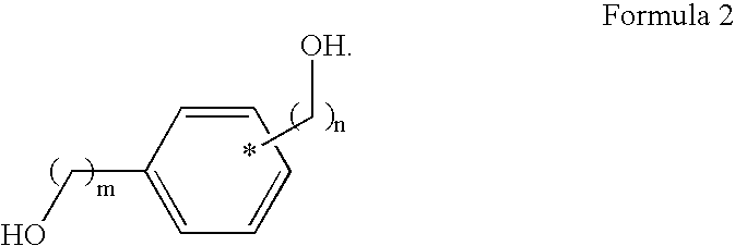
- the hydroxyl compound has a structure shown in Formula 2
- R 1 is (CH 2 ) k Si(OR′) 3 ;
- R′ is selected from the group consisting of H, linear C 1 -C 10 alkyl, and branched C 1 -C 10 alkyl;
- k is an integer ranging from 1 to 10;
- m is an integer ranging from 0 to 5; and,
- n is an integer ranging from 1 to 5.
- a hard mask composition that includes the cross-linking polymer and an organic solvent.
- the hard mask composition serves as an anti-reflection layer and has a relatively higher or similar etching selectivity to that of a photoresist material to secure the etching selectivity to a bottom underlying layer when an underlying layer pattern is formed.
- a method for manufacturing a semiconductor device to form a uniform pattern using the hard mask composition includes coating a hard mask film on an underlying layer, patterning the hard mask film to form a hard mask pattern, and patterning the underlying layer using the hard mask pattern as an etching mask to form an underlying pattern.
- the hard mask film is formed of the hard mask composition disclosed above.
- FIG. 1 is a cross-sectional diagram illustrating a multi-layer structure of a conventional process including a hard mask film
- FIGS. 2 a through 2 d are cross-sectional diagrams illustrating a disclosed method for forming a pattern of a semiconductor device.
- FIG. 3 is a SEM photograph illustrating a photoresist pattern obtained from Example 1.
- FIG. 4 is a SEM photograph illustrating an underlying layer pattern after an etching process of Example 1.
- a cross-linking polymer that includes a silicon compound and a hydroxyl compound.
- the silicon compound has a structure shown in Formula 1
- the hydroxyl compound has a structure shown in Formula 2
- R 1 is (CH 2 ) k Si(OR′) 3 ;
- R′ is selected from the group consisting of H, linear C 1 -C 10 alkyl, and branched C 1 -C 10 alkyl;
- k is an integer ranging from 1 to 10;
- m is an integer ranging from 0 to 5; and,
- n is an integer ranging from 1 to 5.
- the silicon compound preferably has a molecular weight ranging from 300 to 30,000. Furthermore, the silicon compound is preferably PSS-octa(trimethoxysilylmethyl) substituted or PSS-octa(trimethoxysilylethyl) substituted.
- the silicon compound causes a cross-linking reaction between compounds to improve an etching selectivity of a hard mask film.
- the silicon compound includes Si in an amount ranging from 15 wt % to 45 wt %, based on the total weight of the silicon compound, thereby forming a cross-linking reaction between an oxygen included in etching gas and a silicon element
- a hard mask film of the present invention secures an etching selectivity to an underlying layer.
- the silicon compound of Formula 1 is obtained by reacting (a) a compound of Formula 3
- R is (CH 2 ) k SiCl 3 , and k is an integer ranging from 1 to 10, and (b) a C 1 -C 10 alkyl alcohol.
- the reaction is performed by combining the compound of Formula 3 and the alcohol in a weight ratio of 1:8 at room temperature.
- the hydroxyl compound of Formula 2 preferably has a molecular weight ranging from 100 to 10,000.
- the hydroxyl compound is represented by a compound including a benzene ring and a diol structure.
- the hydroxyl compound is represented by resorcinol or 1,4-benzenedimethanol.
- the hydroxyl compound is present in an amount ranging from 10 parts by weight to 80 parts by weight, based on 100 parts by weight of the silicon compound of Formula 1.
- the hydroxyl compound shows a high light absorbance to DUV, specifically ArF (193 nm)
- reflected lights and standing waves generated from the bottom layer are removed to increase the light absorbance of the wavelength region.
- the hydroxyl compound reacts with the silicon compound of Formula 1 to form a cross-linking polymer.
- the cross-linking polymer preferably has a molecular weight ranging from 500 to 50,000. If the molecular weight of the disclosed cross-linking polymer is less than 500, then the coating characteristic of the disclosed hard mask composition is degraded, and the hard mask film is dissolved in a photoresist solvent when a subsequent photoresist is formed. On the other hand, because a cross-linking density in the disclosed hard mask composition increases when the molecular weight of the disclosed cross-linking polymer exceeds 50,000, the etching selectivity of the disclosed hard mask film exceeds that of the photoresist film. As the result, the etching speed is decreased.
- the disclosed cross-linking polymer forms a cross-linking even at room temperature, the cross-linking density increases in a subsequent baking process.
- a hard mask composition that includes the disclosed cross-linking polymer and an organic solvent.
- the organic solvent is selected from the group consisting of ethyl 3-ethoxypropionate, methyl 3-methoxypropionate, cyclohexanone, propylene glycol monomethyl ether acetate (PGMEA), 2-heptanone, ethyl lactate, and mixtures thereof.
- the organic solvent is present in an amount ranging from 500 parts by weight to 10,000 parts by weight, based on 100 parts by weight of the cross-linking polymer.
- the hard mask film having a sufficient thickness cannot be obtained when the organic solvent is present in the amount of more than 10,000 parts by weight.
- the hard mask film is thickly formed so that it is difficult to etch a pattern vertically.
- the disclosed hard mask composition also can include a catalyst selected from the group consisting of a thermal acid generator, a photoacid generator and combinations thereof.
- the catalyst is useful to increase the cross-linking between the compounds during baking.
- the addition amount of catalyst can be adjustably selected to serve as a catalyst.
- the catalyst may be present in a range from 0.1 parts by weight to 10 parts by weight, based on 100 parts by weight of the disclosed cross-linking polymer.
- thermal acid generator is selected from the group consisting of a compound of Formula 4a
- A is a functional group comprising a sulfonyl group, and n is 0 or 1.
- the sulfonyl group is
- the thermal acid generator is 2-hydroxylhexyl p-toluenylsulfonate.
- the photoacid generator preferably is selected from the group consisting of phthalimidotrifluoromethane sulfonate, dinitrobenzyltosylate, n-decyldisulfone, naphtylimidotrifluoromethane sulfonate, diphenyl p-methoxyphenyl sulfonium triflate, diphenyl p-toluenyl sulfonium triflate, diphenyl p-isobutylphenyl sulfonium triflate, triphenylhexafluoro arsenate, triphenylhexafluoro antimonate, triphenylsulfonium triflate, dibutylnaphtyl sulfonium triflate, and mixtures thereof.
- the catalyst serves as a catalyst for activating the cross-linking reaction between the silicon compound and an —OH group of the hydroxyl compound of Formula 2.
- a thermal process or baking process is performed after the hard mask composition (containing the catalyst, such the thermal acid generator or the photoacid generator) is coated on a wafer, acid is generated from the catalyst, and the above-described cross-linking reaction occurs by the generated acid.
- the hard mask film which is not dissolved in the photoresist solvent, is formed.
- the above-described hard mask composition contains a cross-linking structure including a benzene ring having a high light absorbance to short wavelength
- the composition serves as an anti-reflection layer to remove scattered reflection lights and standing waves generated from the bottom layer in an exposure process and also secures an etching selectivity to an underlying layer by the cross-linking structure between the compounds.
- the method includes coating a hard mask film on an underlying layer, patterning the hard mask film to form a hard mask pattern, and patterning the underlying layer using the hard mask pattern as an etching mask to form an underlying pattern.
- the hard mask film is formed of the hard mask composition disclosed above.
- the method also can include forming an amorphous carbon layer or a polymer layer having a high carbon content on the underlying layer before coating the disclosed composition for hard mask to secure the etching selectivity of the hard mask film.
- the disclosed hard mask film may be formed as a single layer to simplify the process step.
- the disclosed hard mask film is formed with equipment for forming a conventional photoresist film. It is easy to remove the hard mask film by a common removal process with a thinner, an alkali solvent or a fluorine gas.
- an underlying layer 23 is formed over a substrate 21 .
- the disclosed composition for hard mask is coated over the underlying layer 23 , and then a baking process is performed to form a hard mask film 25 .
- the underlying layer includes an oxide nitride film or an oxide film.
- the baking process is performed at a temperature ranging from 100° C. to 300° C. for 1 minute to 5 minutes.
- the cross-linking density in the hard mask film increases by acid generated from a thermal acid generator or a photoacid generator in baking process.
- the hard mask film has a thickness ranging from 500 ⁇ to 2000 ⁇ .
- an amorphous carbon layer or a polymer having high carbon content is further formed to be used as a double-layered hard mask film.
- a conventional chemical amplification-type photoresist composition is coated on the hard mask film 25 , and then baked to form a photoresist film 27 (see FIG. 2 a ).
- An exposure and developing process is performed on the photoresist film 27 of FIG. 2 a to form a photoresist pattern 27 - 1 .
- an etching process is performed on the hard mask film 25 with the photoresist pattern 27 - 1 as an etching mask to form a hard mask film pattern 25 - 1 as shown in FIG. 2 b.
- an etching process is performed on the underlying layer 23 with a deposition pattern including the photoresist pattern 27 - 1 and the hard mask pattern 25 - 1 of FIG. 2 b as an etching mask to form an underlying layer pattern 23 - 1 as shown in FIG. 2 c.
- the etching process is performed with an etching gas selected from the group consisting of Cl 2 , Ar, N 2 O 2 , CF 4 , C 2 F 6 , and mixtures thereof.
- the power can be variously applied depending on etching equipment, used gases and process kinds in the etching process.
- the power is applied by a source RF power ranging from 300 W to 1000 W and the bias power ranging from 0 W to 300 W.
- a removal process is performed with a conventional thinner composition, an alkali solvent, or a fluorine gas, to remove the photoresist pattern 27 - 1 and the hard mask pattern 25 - 1 remaining after the etching process so that the underlying layer pattern 23 - 1 is formed over the substrate 21 as shown in FIG. 2 d.
- the disclosed hard mask composition and the disclosed method for manufacturing a semiconductor device are then applied to a process for forming an ultra fine pattern with DUV light sources of short wavelength such as KrF, VUV, EUV, E-beam, X-ray or ion-beam, preferably ArF (193 nm).
- compositions will be described in detail by referring to examples below, which are not intended to limit the present invention.
- An oxide nitride film as an underlying layer was formed on a silicon wafer treated with hexamethyldisilazane (HMDS), and the hard mask composition (3 ml) of Preparation Example 1 was spin-coated thereon with 3000 rpm. Then, the resulting structure was baked at about 200° C. for about 90 seconds to form a hard mask film having a thickness of 920 ⁇ .
- HMDS hexamethyldisilazane
- TMAH tetramethylammonium hydroxide
- the hard mask pattern was etched with the photoresist pattern as an etching mask to form a hard mask pattern, and an etching process was performed on the underlying layer with the same etching process condition with the hard mask pattern as an etching mask to form a 80 nm L/S underlying layer pattern (see FIG. 4 ).
- the etching process was performed with CF 4 /Ar mixture etching gas (RF power: about 700 W, bias power: about 150 W).
- Example 1 The procedure of Example 1 was repeated using the composition for hard mask of Preparation Example 2 instead of the composition of Preparation Example 1 to obtain a 80 nm L/S underlying layer pattern.
- a silicon oxide nitride film as an underlying layer was formed on a silicon wafer treated with HMDS, and an amorphous carbon layer having a thickness of 200 nm was formed thereon by a Chemical Vapor Deposition (CVD) method. Then, the composition (3 ml) for hard mask of Preparation Example 1 was spin-coated thereon with 3000 rpm, and baked at about 200° C. for about 90 seconds to form a hard mask film having a thickness of 920 ⁇ .
- CVD Chemical Vapor Deposition
- TMAH tetramethylammonium hydroxide
- the hard mask pattern was etched with the photoresist pattern as an etching mask to form a hard mask pattern, and an etching process was performed on the underlying layer with the same etching process condition with the hard mask pattern as an etching mask to form a 80 nm L/S underlying layer pattern.
- the etching process was performed with CF 4 /Ar mixture etching gas (RF power: about 700 W, bias power: about 150 W).
- Example 3 The procedure of Example 3 was repeated using the composition for hard mask of Preparation Example 2 instead of the composition of Preparation Example 1 to obtain a 80 nm L/S underlying layer pattern.
- a disclosed composition for hard mask including a cross-linking polymer (consisting of a silicon compound and a hydroxyl compound) and an organic solvent.
- the disclosed composition is used as a hard mask film that has an anti-reflection layer and an excellent etching selectivity in a subsequent etching process so that a uniform underlying layer pattern is obtained. Also, a pattern formation process is simplified to reduce process cost.
Abstract
Description
- 1. Field of the Disclosure
- The disclosure generally relates to a hard mask composition and a method for manufacturing a semiconductor device using the composition.
- 2. Brief Description of Related Technology
- As the fields of application of semiconductor devices have expanded, there has been a need to manufacture a memory device of high capacity with improved integrity. Semiconductor manufacturing processes necessarily include a lithography process for forming a line pattern (such as a gate line and a bit line), or a contact hole pattern (such as a bit line contact).
- In order to form a critical dimension (CD) below 0.07 μm, the lithography process has been developed with Deep Ultra Violet (DUV) light sources of short wavelength such as ArF (193 nm) or VUV (157 nm) instead of long wavelength light sources such as I-line or KrF (248 nm).
- Generally, the lithography process includes a process for forming a bottom anti-reflection layer in the bottom of the photoresist film so as to prevent scattered reflection from a bottom layer of a photoresist film and remove standing waves resulting from thickness variation of a photoresist film.
- On the other hand, the thickness of photoresist layers also becomes smaller to prevent photoresist patterns from collapsing during the lithography process. As a result, it is difficult to secure an etching selectivity of a photoresist pattern as an etching mask on an underlying layer during the etching process.
- In order to secure the etching selectivity, a multi-layer hard mask film having the etching rate relatively higher than that of the photoresist pattern is formed between the underlying layer and the photoresist pattern in the conventional method for manufacturing a semiconductor device. For example, the above-described conventional method includes forming a multi-layer hard mask film including an
amorphous carbon film 3 andinsulating film 5 on an underlying layer 1 over a semiconductor substrate, and then sequentially forming ananti-reflection film 7 and a photoresist pattern 9 (seeFIG. 1 ). - Consequently, films that serve as the organic anti-reflection layer and the hard mask film are required to simplify the process.
- A conventional composition for the organic anti-reflection layer satisfies the following conditions.
- First, while an anti-reflection layer is coated and then a photoresist layer is coated, the anti-reflection layer should not be dissolved by an organic solvent in a photoresist composition. Thus, the anti-reflection layer is designed to have a cross-linking structure in a process for coating an anti-reflection layer composition and baking the composition to deposit the anti-reflection layer. Here, other chemical materials should not be generated as by-products.
- Second, the composition is required to contain a material having a high light absorbance to light sources to inhibit scattered reflection from a bottom layer.
- Third, the composition is required to contain a catalyst for activating the cross-linking reaction in the process for depositing the anti-reflection composition.
- Moreover, a film used as the hard mask film is required to have the excellent etching selectivity to the bottom-underlying layer.
- Disclosed herein is a cross-linking polymer that includes a silicon compound and a hydroxyl compound. The silicon compound has a structure shown in Formula 1
-

- The hydroxyl compound has a structure shown in Formula 2
-

- In the foregoing Formulas 1 and 2, R1 is (CH2)kSi(OR′)3; R′ is selected from the group consisting of H, linear C1-C10 alkyl, and branched C1-C10 alkyl; k is an integer ranging from 1 to 10; m is an integer ranging from 0 to 5; and, n is an integer ranging from 1 to 5.
- Also disclosed herein is a hard mask composition that includes the cross-linking polymer and an organic solvent. The hard mask composition serves as an anti-reflection layer and has a relatively higher or similar etching selectivity to that of a photoresist material to secure the etching selectivity to a bottom underlying layer when an underlying layer pattern is formed.
- Also, disclosed herein is a method for manufacturing a semiconductor device to form a uniform pattern using the hard mask composition. The method includes coating a hard mask film on an underlying layer, patterning the hard mask film to form a hard mask pattern, and patterning the underlying layer using the hard mask pattern as an etching mask to form an underlying pattern. The hard mask film is formed of the hard mask composition disclosed above.
- Additional features of the invention may become apparent to those skilled in the art from a review of the following detailed description, taken in conjunction with the drawings, the examples, and the appended claims.
- For a more complete understanding of the invention, reference should be made to the following detailed description and accompanying drawings, wherein:
-
FIG. 1 is a cross-sectional diagram illustrating a multi-layer structure of a conventional process including a hard mask film; -
FIGS. 2 a through 2 d are cross-sectional diagrams illustrating a disclosed method for forming a pattern of a semiconductor device.; -
FIG. 3 is a SEM photograph illustrating a photoresist pattern obtained from Example 1; and, -
FIG. 4 is a SEM photograph illustrating an underlying layer pattern after an etching process of Example 1. - While the disclosed polymer, composition, and method are susceptible of embodiments in various forms, there are illustrated in the drawing (and will hereafter be described) specific embodiments of the invention, with the understanding that the disclosure is intended to be illustrative, and is not intended to limit the invention to the specific embodiments described and illustrated herein.
- Disclosed herein is a cross-linking polymer that includes a silicon compound and a hydroxyl compound. The silicon compound has a structure shown in Formula 1
-

- The hydroxyl compound has a structure shown in Formula 2
-
- In the foregoing Formulas 1 and 2, R1 is (CH2)kSi(OR′)3; R′ is selected from the group consisting of H, linear C1-C10 alkyl, and branched C1-C10 alkyl; k is an integer ranging from 1 to 10; m is an integer ranging from 0 to 5; and, n is an integer ranging from 1 to 5.
- The silicon compound preferably has a molecular weight ranging from 300 to 30,000. Furthermore, the silicon compound is preferably PSS-octa(trimethoxysilylmethyl) substituted or PSS-octa(trimethoxysilylethyl) substituted.
- The silicon compound causes a cross-linking reaction between compounds to improve an etching selectivity of a hard mask film. Preferably, the silicon compound includes Si in an amount ranging from 15 wt % to 45 wt %, based on the total weight of the silicon compound, thereby forming a cross-linking reaction between an oxygen included in etching gas and a silicon element As a result, a hard mask film of the present invention secures an etching selectivity to an underlying layer.
- The silicon compound of Formula 1 is obtained by reacting (a) a compound of Formula 3
-

- wherein R is (CH2)kSiCl3, and k is an integer ranging from 1 to 10, and (b) a C1-C10 alkyl alcohol. The reaction is performed by combining the compound of Formula 3 and the alcohol in a weight ratio of 1:8 at room temperature.
- The hydroxyl compound of Formula 2 preferably has a molecular weight ranging from 100 to 10,000. The hydroxyl compound is represented by a compound including a benzene ring and a diol structure. For example, the hydroxyl compound is represented by resorcinol or 1,4-benzenedimethanol. Preferably, the hydroxyl compound is present in an amount ranging from 10 parts by weight to 80 parts by weight, based on 100 parts by weight of the silicon compound of Formula 1.
- Because the hydroxyl compound shows a high light absorbance to DUV, specifically ArF (193 nm), reflected lights and standing waves generated from the bottom layer are removed to increase the light absorbance of the wavelength region. Also, the hydroxyl compound reacts with the silicon compound of Formula 1 to form a cross-linking polymer.
- The cross-linking polymer preferably has a molecular weight ranging from 500 to 50,000. If the molecular weight of the disclosed cross-linking polymer is less than 500, then the coating characteristic of the disclosed hard mask composition is degraded, and the hard mask film is dissolved in a photoresist solvent when a subsequent photoresist is formed. On the other hand, because a cross-linking density in the disclosed hard mask composition increases when the molecular weight of the disclosed cross-linking polymer exceeds 50,000, the etching selectivity of the disclosed hard mask film exceeds that of the photoresist film. As the result, the etching speed is decreased.
- Although the disclosed cross-linking polymer forms a cross-linking even at room temperature, the cross-linking density increases in a subsequent baking process.
- Also, disclosed herein is a hard mask composition that includes the disclosed cross-linking polymer and an organic solvent.
- Any of the organic solvents useful as a conventional solvent for an anti-reflection layer composition can be used. Preferably, the organic solvent is selected from the group consisting of ethyl 3-ethoxypropionate, methyl 3-methoxypropionate, cyclohexanone, propylene glycol monomethyl ether acetate (PGMEA), 2-heptanone, ethyl lactate, and mixtures thereof. Preferably, the organic solvent is present in an amount ranging from 500 parts by weight to 10,000 parts by weight, based on 100 parts by weight of the cross-linking polymer. The hard mask film having a sufficient thickness cannot be obtained when the organic solvent is present in the amount of more than 10,000 parts by weight. When the organic solvent is present in the amount of less than 500 parts by weight, the hard mask film is thickly formed so that it is difficult to etch a pattern vertically.
- The disclosed hard mask composition also can include a catalyst selected from the group consisting of a thermal acid generator, a photoacid generator and combinations thereof. The catalyst is useful to increase the cross-linking between the compounds during baking.
- The addition amount of catalyst can be adjustably selected to serve as a catalyst. For example, the catalyst may be present in a range from 0.1 parts by weight to 10 parts by weight, based on 100 parts by weight of the disclosed cross-linking polymer.
- Any of the conventional thermal acid generators can be used. Preferably, the thermal acid generator is selected from the group consisting of a compound of Formula 4a
-

- a compound of Formula 4b
-

- and mixtures thereof, wherein A is a functional group comprising a sulfonyl group, and n is 0 or 1.
- Preferably, the sulfonyl group is
-

- More preferably, the thermal acid generator is 2-hydroxylhexyl p-toluenylsulfonate.
- The photoacid generator preferably is selected from the group consisting of phthalimidotrifluoromethane sulfonate, dinitrobenzyltosylate, n-decyldisulfone, naphtylimidotrifluoromethane sulfonate, diphenyl p-methoxyphenyl sulfonium triflate, diphenyl p-toluenyl sulfonium triflate, diphenyl p-isobutylphenyl sulfonium triflate, triphenylhexafluoro arsenate, triphenylhexafluoro antimonate, triphenylsulfonium triflate, dibutylnaphtyl sulfonium triflate, and mixtures thereof.
- The catalyst serves as a catalyst for activating the cross-linking reaction between the silicon compound and an —OH group of the hydroxyl compound of Formula 2. For example, when a thermal process or baking process is performed after the hard mask composition (containing the catalyst, such the thermal acid generator or the photoacid generator) is coated on a wafer, acid is generated from the catalyst, and the above-described cross-linking reaction occurs by the generated acid. As a result, the hard mask film, which is not dissolved in the photoresist solvent, is formed.
- Because the above-described hard mask composition contains a cross-linking structure including a benzene ring having a high light absorbance to short wavelength, the composition serves as an anti-reflection layer to remove scattered reflection lights and standing waves generated from the bottom layer in an exposure process and also secures an etching selectivity to an underlying layer by the cross-linking structure between the compounds.
- Also, disclosed herein is a method for manufacturing a semiconductor device. The method includes coating a hard mask film on an underlying layer, patterning the hard mask film to form a hard mask pattern, and patterning the underlying layer using the hard mask pattern as an etching mask to form an underlying pattern. The hard mask film is formed of the hard mask composition disclosed above. The method also can include forming an amorphous carbon layer or a polymer layer having a high carbon content on the underlying layer before coating the disclosed composition for hard mask to secure the etching selectivity of the hard mask film. The disclosed hard mask film may be formed as a single layer to simplify the process step. The disclosed hard mask film is formed with equipment for forming a conventional photoresist film. It is easy to remove the hard mask film by a common removal process with a thinner, an alkali solvent or a fluorine gas.
- Hereinafter, the disclosed method for forming a pattern of a semiconductor device described in detail. Referring to
FIG. 2 a, anunderlying layer 23 is formed over asubstrate 21. The disclosed composition for hard mask is coated over theunderlying layer 23, and then a baking process is performed to form ahard mask film 25. The underlying layer includes an oxide nitride film or an oxide film. - The baking process is performed at a temperature ranging from 100° C. to 300° C. for 1 minute to 5 minutes. Here, the cross-linking density in the hard mask film increases by acid generated from a thermal acid generator or a photoacid generator in baking process. The hard mask film has a thickness ranging from 500 Å to 2000 Å. Before the hard mask film is formed, an amorphous carbon layer or a polymer having high carbon content is further formed to be used as a double-layered hard mask film. A conventional chemical amplification-type photoresist composition is coated on the
hard mask film 25, and then baked to form a photoresist film 27 (seeFIG. 2 a). - An exposure and developing process is performed on the
photoresist film 27 ofFIG. 2 a to form a photoresist pattern 27-1. Then, an etching process is performed on thehard mask film 25 with the photoresist pattern 27-1 as an etching mask to form a hard mask film pattern 25-1 as shown inFIG. 2 b. Thereafter, an etching process is performed on theunderlying layer 23 with a deposition pattern including the photoresist pattern 27-1 and the hard mask pattern 25-1 ofFIG. 2 b as an etching mask to form an underlying layer pattern 23-1 as shown inFIG. 2 c. - Preferably, the etching process is performed with an etching gas selected from the group consisting of Cl2, Ar, N2O2, CF4, C2F6, and mixtures thereof. The power can be variously applied depending on etching equipment, used gases and process kinds in the etching process. Preferably, the power is applied by a source RF power ranging from 300 W to 1000 W and the bias power ranging from 0 W to 300 W.
- Thereafter, a removal process is performed with a conventional thinner composition, an alkali solvent, or a fluorine gas, to remove the photoresist pattern 27-1 and the hard mask pattern 25-1 remaining after the etching process so that the underlying layer pattern 23-1 is formed over the
substrate 21 as shown inFIG. 2 d. The disclosed hard mask composition and the disclosed method for manufacturing a semiconductor device are then applied to a process for forming an ultra fine pattern with DUV light sources of short wavelength such as KrF, VUV, EUV, E-beam, X-ray or ion-beam, preferably ArF (193 nm). - Additionally, there is provided herein a semiconductor device manufactured by the disclosed method including the pattern formation process.
- The disclosed compositions will be described in detail by referring to examples below, which are not intended to limit the present invention.
- (1-1) PSS-octa(trimethoxysilylmethyl) substituted (30 g) was added in methanol (500 ml), and stirred at room temperature for 30 minutes. Then, resorcinol (3 g) was added in the resulting mixture, and stirred at room temperature for 1 hour. Thereafter, the resulting mixture was vacuum-distilled at below 40° C., and washed with methanol (200 ml×2). Next, the resulting mixture was filtered and dehydrated to obtain a cross-linking polymer (yield: 31 g, molecular weight: 3,400).
- (1-2) The cross-linking polymer (5 g) obtained from Preparation Example 1-1 was dissolved in propylene glycol monomethyl ether acetate (PGMEA) (100 g). Then, the resulting mixture was filtered with a 0.2 μm filter to obtain a disclosed hard mask composition.
- (2-1) PSS-octa(trimethoxysilylethyl) substituted (30 g) was added in methanol (500 ml), and stirred at room temperature for 30 minutes. Then, resorcinol (3 g) was added in the resulting mixture, and stirred at room temperature for 1 hour. Thereafter, the resulting mixture was vacuum-distilled at below 40° C., and washed with methanol (200 ml×2). Next, the resulting mixture was filtered and dehydrated to obtain a cross-linking polymer (yield: 29.2 g, molecular weight: 3,620).
- (2-2) In propylene glycol monomethyl ether acetate (PGMEA) (100 g) was dissolved the cross-linking polymer (5 g) obtained from Preparation Example 2-1, 2-hydroxyhexyl p-toluenylsulfonate (0.4 g) as a thermal acid generator and triphenylsufonium triflate (0.05 g) as a photoacid generator. Then, the resulting mixture was filtered with a 0.2 μm filter to obtain a disclosed hard mask composition.
- An oxide nitride film as an underlying layer was formed on a silicon wafer treated with hexamethyldisilazane (HMDS), and the hard mask composition (3 ml) of Preparation Example 1 was spin-coated thereon with 3000 rpm. Then, the resulting structure was baked at about 200° C. for about 90 seconds to form a hard mask film having a thickness of 920 Å.
- A photoresist film (Shin-Etsu Co., X-121) for ArF (193 nm) was coated at a thickness of 1700 Å on the hard mask film, soft-baked at about 120° C. for about 90 seconds, exposed with an ArF scanner (NA=0.85, ASML Co.), and then post-baked at about 120° C. for about 90 seconds. After post-baking, the film was developed in 2.38 wt % tetramethylammonium hydroxide (TMAH) aqueous solution to obtain 80 nm L/S photoresist pattern (see
FIG. 3 ). - Thereafter, the hard mask pattern was etched with the photoresist pattern as an etching mask to form a hard mask pattern, and an etching process was performed on the underlying layer with the same etching process condition with the hard mask pattern as an etching mask to form a 80 nm L/S underlying layer pattern (see
FIG. 4 ). Here, the etching process was performed with CF4/Ar mixture etching gas (RF power: about 700 W, bias power: about 150 W). - The procedure of Example 1 was repeated using the composition for hard mask of Preparation Example 2 instead of the composition of Preparation Example 1 to obtain a 80 nm L/S underlying layer pattern.
- A silicon oxide nitride film as an underlying layer was formed on a silicon wafer treated with HMDS, and an amorphous carbon layer having a thickness of 200 nm was formed thereon by a Chemical Vapor Deposition (CVD) method. Then, the composition (3 ml) for hard mask of Preparation Example 1 was spin-coated thereon with 3000 rpm, and baked at about 200° C. for about 90 seconds to form a hard mask film having a thickness of 920 Å.
- A photoresist film (Shin-Etsu Co., X-121) for ArF (193 nm) was coated at a thickness of 1700 Å on the hard mask film, soft-baked at about 120° C. for about 90 seconds, exposed with an ArF scanner (NA=0.85, ASML Co.), and then post-baked at about 120° C. for about 90 seconds. After post-baking, the film was developed in 2.38 wt % tetramethylammonium hydroxide (TMAH) aqueous solution to obtain 80 nm L/S photoresist pattern.
- Thereafter, the hard mask pattern was etched with the photoresist pattern as an etching mask to form a hard mask pattern, and an etching process was performed on the underlying layer with the same etching process condition with the hard mask pattern as an etching mask to form a 80 nm L/S underlying layer pattern. Here, the etching process was performed with CF4/Ar mixture etching gas (RF power: about 700 W, bias power: about 150 W).
- The procedure of Example 3 was repeated using the composition for hard mask of Preparation Example 2 instead of the composition of Preparation Example 1 to obtain a 80 nm L/S underlying layer pattern.
- As described above, there is provided a disclosed composition for hard mask including a cross-linking polymer (consisting of a silicon compound and a hydroxyl compound) and an organic solvent. The disclosed composition is used as a hard mask film that has an anti-reflection layer and an excellent etching selectivity in a subsequent etching process so that a uniform underlying layer pattern is obtained. Also, a pattern formation process is simplified to reduce process cost.
- The foregoing description is given for clearness of understanding only, and no unnecessary limitations should be understood therefrom, as modifications within the scope of the invention may be apparent to those having ordinary skill in the art.
Claims (21)


Applications Claiming Priority (2)
| Application Number | Priority Date | Filing Date | Title |
|---|---|---|---|
| KR10-2005-0135270 | 2005-12-30 | ||
| KR20050135270 | 2005-12-30 |
Publications (2)
| Publication Number | Publication Date |
|---|---|
| US20070154838A1 true US20070154838A1 (en) | 2007-07-05 |
| US7449538B2 US7449538B2 (en) | 2008-11-11 |
Family
ID=38224859
Family Applications (1)
| Application Number | Title | Priority Date | Filing Date |
|---|---|---|---|
| US11/421,897 Active 2027-07-06 US7449538B2 (en) | 2005-12-30 | 2006-06-02 | Hard mask composition and method for manufacturing semiconductor device |
Country Status (2)
| Country | Link |
|---|---|
| US (1) | US7449538B2 (en) |
| KR (1) | KR100787332B1 (en) |
Cited By (123)
| Publication number | Priority date | Publication date | Assignee | Title |
|---|---|---|---|---|
| US20080153299A1 (en) * | 2006-12-22 | 2008-06-26 | Hynix Semiconductor Inc. | Semiconductor Device And Method For Forming A Pattern In The Same With Double Exposure Technology |
| US20150371861A1 (en) * | 2014-06-23 | 2015-12-24 | Applied Materials, Inc. | Protective silicon oxide patterning |
| US9299538B2 (en) | 2014-03-20 | 2016-03-29 | Applied Materials, Inc. | Radial waveguide systems and methods for post-match control of microwaves |
| US9299537B2 (en) | 2014-03-20 | 2016-03-29 | Applied Materials, Inc. | Radial waveguide systems and methods for post-match control of microwaves |
| US9343272B1 (en) | 2015-01-08 | 2016-05-17 | Applied Materials, Inc. | Self-aligned process |
| US9349605B1 (en) | 2015-08-07 | 2016-05-24 | Applied Materials, Inc. | Oxide etch selectivity systems and methods |
| US9355863B2 (en) | 2012-12-18 | 2016-05-31 | Applied Materials, Inc. | Non-local plasma oxide etch |
| US9355922B2 (en) | 2014-10-14 | 2016-05-31 | Applied Materials, Inc. | Systems and methods for internal surface conditioning in plasma processing equipment |
| US9355862B2 (en) | 2014-09-24 | 2016-05-31 | Applied Materials, Inc. | Fluorine-based hardmask removal |
| US9355856B2 (en) | 2014-09-12 | 2016-05-31 | Applied Materials, Inc. | V trench dry etch |
| US9362130B2 (en) | 2013-03-01 | 2016-06-07 | Applied Materials, Inc. | Enhanced etching processes using remote plasma sources |
| US9368364B2 (en) | 2014-09-24 | 2016-06-14 | Applied Materials, Inc. | Silicon etch process with tunable selectivity to SiO2 and other materials |
| US9373522B1 (en) | 2015-01-22 | 2016-06-21 | Applied Mateials, Inc. | Titanium nitride removal |
| US9373517B2 (en) | 2012-08-02 | 2016-06-21 | Applied Materials, Inc. | Semiconductor processing with DC assisted RF power for improved control |
| US9378978B2 (en) | 2014-07-31 | 2016-06-28 | Applied Materials, Inc. | Integrated oxide recess and floating gate fin trimming |
| US9378969B2 (en) | 2014-06-19 | 2016-06-28 | Applied Materials, Inc. | Low temperature gas-phase carbon removal |
| US9384997B2 (en) | 2012-11-20 | 2016-07-05 | Applied Materials, Inc. | Dry-etch selectivity |
| US9385028B2 (en) | 2014-02-03 | 2016-07-05 | Applied Materials, Inc. | Air gap process |
| US9390937B2 (en) | 2012-09-20 | 2016-07-12 | Applied Materials, Inc. | Silicon-carbon-nitride selective etch |
| US9396989B2 (en) | 2014-01-27 | 2016-07-19 | Applied Materials, Inc. | Air gaps between copper lines |
| US9406523B2 (en) | 2014-06-19 | 2016-08-02 | Applied Materials, Inc. | Highly selective doped oxide removal method |
| US9412608B2 (en) | 2012-11-30 | 2016-08-09 | Applied Materials, Inc. | Dry-etch for selective tungsten removal |
| US9418858B2 (en) | 2011-10-07 | 2016-08-16 | Applied Materials, Inc. | Selective etch of silicon by way of metastable hydrogen termination |
| US9425058B2 (en) | 2014-07-24 | 2016-08-23 | Applied Materials, Inc. | Simplified litho-etch-litho-etch process |
| US9437451B2 (en) | 2012-09-18 | 2016-09-06 | Applied Materials, Inc. | Radical-component oxide etch |
| US9449846B2 (en) | 2015-01-28 | 2016-09-20 | Applied Materials, Inc. | Vertical gate separation |
| US9449845B2 (en) | 2012-12-21 | 2016-09-20 | Applied Materials, Inc. | Selective titanium nitride etching |
| US9472417B2 (en) | 2013-11-12 | 2016-10-18 | Applied Materials, Inc. | Plasma-free metal etch |
| US9472412B2 (en) | 2013-12-02 | 2016-10-18 | Applied Materials, Inc. | Procedure for etch rate consistency |
| US9478432B2 (en) | 2014-09-25 | 2016-10-25 | Applied Materials, Inc. | Silicon oxide selective removal |
| US9496167B2 (en) | 2014-07-31 | 2016-11-15 | Applied Materials, Inc. | Integrated bit-line airgap formation and gate stack post clean |
| US9493879B2 (en) | 2013-07-12 | 2016-11-15 | Applied Materials, Inc. | Selective sputtering for pattern transfer |
| US9502258B2 (en) | 2014-12-23 | 2016-11-22 | Applied Materials, Inc. | Anisotropic gap etch |
| US9499898B2 (en) | 2014-03-03 | 2016-11-22 | Applied Materials, Inc. | Layered thin film heater and method of fabrication |
| US9553102B2 (en) | 2014-08-19 | 2017-01-24 | Applied Materials, Inc. | Tungsten separation |
| US9576809B2 (en) | 2013-11-04 | 2017-02-21 | Applied Materials, Inc. | Etch suppression with germanium |
| US9607856B2 (en) | 2013-03-05 | 2017-03-28 | Applied Materials, Inc. | Selective titanium nitride removal |
| US9659753B2 (en) | 2014-08-07 | 2017-05-23 | Applied Materials, Inc. | Grooved insulator to reduce leakage current |
| US9659792B2 (en) | 2013-03-15 | 2017-05-23 | Applied Materials, Inc. | Processing systems and methods for halide scavenging |
| US9691645B2 (en) | 2015-08-06 | 2017-06-27 | Applied Materials, Inc. | Bolted wafer chuck thermal management systems and methods for wafer processing systems |
| US9721789B1 (en) | 2016-10-04 | 2017-08-01 | Applied Materials, Inc. | Saving ion-damaged spacers |
| US9728437B2 (en) | 2015-02-03 | 2017-08-08 | Applied Materials, Inc. | High temperature chuck for plasma processing systems |
| US9741593B2 (en) | 2015-08-06 | 2017-08-22 | Applied Materials, Inc. | Thermal management systems and methods for wafer processing systems |
| US9754800B2 (en) | 2010-05-27 | 2017-09-05 | Applied Materials, Inc. | Selective etch for silicon films |
| US9768034B1 (en) | 2016-11-11 | 2017-09-19 | Applied Materials, Inc. | Removal methods for high aspect ratio structures |
| US9773648B2 (en) | 2013-08-30 | 2017-09-26 | Applied Materials, Inc. | Dual discharge modes operation for remote plasma |
| US9842744B2 (en) | 2011-03-14 | 2017-12-12 | Applied Materials, Inc. | Methods for etch of SiN films |
| US9865484B1 (en) | 2016-06-29 | 2018-01-09 | Applied Materials, Inc. | Selective etch using material modification and RF pulsing |
| US9881805B2 (en) | 2015-03-02 | 2018-01-30 | Applied Materials, Inc. | Silicon selective removal |
| US9887096B2 (en) | 2012-09-17 | 2018-02-06 | Applied Materials, Inc. | Differential silicon oxide etch |
| US9885117B2 (en) | 2014-03-31 | 2018-02-06 | Applied Materials, Inc. | Conditioned semiconductor system parts |
| US9934942B1 (en) | 2016-10-04 | 2018-04-03 | Applied Materials, Inc. | Chamber with flow-through source |
| US9947549B1 (en) | 2016-10-10 | 2018-04-17 | Applied Materials, Inc. | Cobalt-containing material removal |
| US9966240B2 (en) | 2014-10-14 | 2018-05-08 | Applied Materials, Inc. | Systems and methods for internal surface conditioning assessment in plasma processing equipment |
| US9978564B2 (en) | 2012-09-21 | 2018-05-22 | Applied Materials, Inc. | Chemical control features in wafer process equipment |
| US10026621B2 (en) | 2016-11-14 | 2018-07-17 | Applied Materials, Inc. | SiN spacer profile patterning |
| US10043674B1 (en) | 2017-08-04 | 2018-08-07 | Applied Materials, Inc. | Germanium etching systems and methods |
| US10043684B1 (en) | 2017-02-06 | 2018-08-07 | Applied Materials, Inc. | Self-limiting atomic thermal etching systems and methods |
| US10049891B1 (en) | 2017-05-31 | 2018-08-14 | Applied Materials, Inc. | Selective in situ cobalt residue removal |
| US10062585B2 (en) | 2016-10-04 | 2018-08-28 | Applied Materials, Inc. | Oxygen compatible plasma source |
| US10062587B2 (en) | 2012-07-18 | 2018-08-28 | Applied Materials, Inc. | Pedestal with multi-zone temperature control and multiple purge capabilities |
| US10062578B2 (en) | 2011-03-14 | 2018-08-28 | Applied Materials, Inc. | Methods for etch of metal and metal-oxide films |
| US10062579B2 (en) | 2016-10-07 | 2018-08-28 | Applied Materials, Inc. | Selective SiN lateral recess |
| US10062575B2 (en) | 2016-09-09 | 2018-08-28 | Applied Materials, Inc. | Poly directional etch by oxidation |
| US10128086B1 (en) | 2017-10-24 | 2018-11-13 | Applied Materials, Inc. | Silicon pretreatment for nitride removal |
| US10163696B2 (en) | 2016-11-11 | 2018-12-25 | Applied Materials, Inc. | Selective cobalt removal for bottom up gapfill |
| US10170336B1 (en) | 2017-08-04 | 2019-01-01 | Applied Materials, Inc. | Methods for anisotropic control of selective silicon removal |
| US10224210B2 (en) | 2014-12-09 | 2019-03-05 | Applied Materials, Inc. | Plasma processing system with direct outlet toroidal plasma source |
| US10242908B2 (en) | 2016-11-14 | 2019-03-26 | Applied Materials, Inc. | Airgap formation with damage-free copper |
| US10256112B1 (en) | 2017-12-08 | 2019-04-09 | Applied Materials, Inc. | Selective tungsten removal |
| US10256079B2 (en) | 2013-02-08 | 2019-04-09 | Applied Materials, Inc. | Semiconductor processing systems having multiple plasma configurations |
| US10283321B2 (en) | 2011-01-18 | 2019-05-07 | Applied Materials, Inc. | Semiconductor processing system and methods using capacitively coupled plasma |
| US10283324B1 (en) | 2017-10-24 | 2019-05-07 | Applied Materials, Inc. | Oxygen treatment for nitride etching |
| US10297458B2 (en) | 2017-08-07 | 2019-05-21 | Applied Materials, Inc. | Process window widening using coated parts in plasma etch processes |
| US10319600B1 (en) | 2018-03-12 | 2019-06-11 | Applied Materials, Inc. | Thermal silicon etch |
| US10319739B2 (en) | 2017-02-08 | 2019-06-11 | Applied Materials, Inc. | Accommodating imperfectly aligned memory holes |
| US10319649B2 (en) | 2017-04-11 | 2019-06-11 | Applied Materials, Inc. | Optical emission spectroscopy (OES) for remote plasma monitoring |
| US10354889B2 (en) | 2017-07-17 | 2019-07-16 | Applied Materials, Inc. | Non-halogen etching of silicon-containing materials |
| US10403507B2 (en) | 2017-02-03 | 2019-09-03 | Applied Materials, Inc. | Shaped etch profile with oxidation |
| US10431429B2 (en) | 2017-02-03 | 2019-10-01 | Applied Materials, Inc. | Systems and methods for radial and azimuthal control of plasma uniformity |
| US10468267B2 (en) | 2017-05-31 | 2019-11-05 | Applied Materials, Inc. | Water-free etching methods |
| US10465294B2 (en) | 2014-05-28 | 2019-11-05 | Applied Materials, Inc. | Oxide and metal removal |
| US10490406B2 (en) | 2018-04-10 | 2019-11-26 | Appled Materials, Inc. | Systems and methods for material breakthrough |
| US10497573B2 (en) | 2018-03-13 | 2019-12-03 | Applied Materials, Inc. | Selective atomic layer etching of semiconductor materials |
| US10504754B2 (en) | 2016-05-19 | 2019-12-10 | Applied Materials, Inc. | Systems and methods for improved semiconductor etching and component protection |
| US10504700B2 (en) | 2015-08-27 | 2019-12-10 | Applied Materials, Inc. | Plasma etching systems and methods with secondary plasma injection |
| US10522371B2 (en) | 2016-05-19 | 2019-12-31 | Applied Materials, Inc. | Systems and methods for improved semiconductor etching and component protection |
| US10541184B2 (en) | 2017-07-11 | 2020-01-21 | Applied Materials, Inc. | Optical emission spectroscopic techniques for monitoring etching |
| US10541246B2 (en) | 2017-06-26 | 2020-01-21 | Applied Materials, Inc. | 3D flash memory cells which discourage cross-cell electrical tunneling |
| US10546729B2 (en) | 2016-10-04 | 2020-01-28 | Applied Materials, Inc. | Dual-channel showerhead with improved profile |
| US10566206B2 (en) | 2016-12-27 | 2020-02-18 | Applied Materials, Inc. | Systems and methods for anisotropic material breakthrough |
| US10573496B2 (en) | 2014-12-09 | 2020-02-25 | Applied Materials, Inc. | Direct outlet toroidal plasma source |
| US10573527B2 (en) | 2018-04-06 | 2020-02-25 | Applied Materials, Inc. | Gas-phase selective etching systems and methods |
| US10593560B2 (en) | 2018-03-01 | 2020-03-17 | Applied Materials, Inc. | Magnetic induction plasma source for semiconductor processes and equipment |
| US10615047B2 (en) | 2018-02-28 | 2020-04-07 | Applied Materials, Inc. | Systems and methods to form airgaps |
| US10629473B2 (en) | 2016-09-09 | 2020-04-21 | Applied Materials, Inc. | Footing removal for nitride spacer |
| US10672642B2 (en) | 2018-07-24 | 2020-06-02 | Applied Materials, Inc. | Systems and methods for pedestal configuration |
| US10679870B2 (en) | 2018-02-15 | 2020-06-09 | Applied Materials, Inc. | Semiconductor processing chamber multistage mixing apparatus |
| US10699879B2 (en) | 2018-04-17 | 2020-06-30 | Applied Materials, Inc. | Two piece electrode assembly with gap for plasma control |
| US10727080B2 (en) | 2017-07-07 | 2020-07-28 | Applied Materials, Inc. | Tantalum-containing material removal |
| US10755941B2 (en) | 2018-07-06 | 2020-08-25 | Applied Materials, Inc. | Self-limiting selective etching systems and methods |
| US10854426B2 (en) | 2018-01-08 | 2020-12-01 | Applied Materials, Inc. | Metal recess for semiconductor structures |
| US10872778B2 (en) | 2018-07-06 | 2020-12-22 | Applied Materials, Inc. | Systems and methods utilizing solid-phase etchants |
| US10886137B2 (en) | 2018-04-30 | 2021-01-05 | Applied Materials, Inc. | Selective nitride removal |
| US10892198B2 (en) | 2018-09-14 | 2021-01-12 | Applied Materials, Inc. | Systems and methods for improved performance in semiconductor processing |
| US10903054B2 (en) | 2017-12-19 | 2021-01-26 | Applied Materials, Inc. | Multi-zone gas distribution systems and methods |
| US10920320B2 (en) | 2017-06-16 | 2021-02-16 | Applied Materials, Inc. | Plasma health determination in semiconductor substrate processing reactors |
| US10920319B2 (en) | 2019-01-11 | 2021-02-16 | Applied Materials, Inc. | Ceramic showerheads with conductive electrodes |
| US10943834B2 (en) | 2017-03-13 | 2021-03-09 | Applied Materials, Inc. | Replacement contact process |
| US10964512B2 (en) | 2018-02-15 | 2021-03-30 | Applied Materials, Inc. | Semiconductor processing chamber multistage mixing apparatus and methods |
| US11049755B2 (en) | 2018-09-14 | 2021-06-29 | Applied Materials, Inc. | Semiconductor substrate supports with embedded RF shield |
| US11062887B2 (en) | 2018-09-17 | 2021-07-13 | Applied Materials, Inc. | High temperature RF heater pedestals |
| US11121002B2 (en) | 2018-10-24 | 2021-09-14 | Applied Materials, Inc. | Systems and methods for etching metals and metal derivatives |
| US11239061B2 (en) | 2014-11-26 | 2022-02-01 | Applied Materials, Inc. | Methods and systems to enhance process uniformity |
| US11257693B2 (en) | 2015-01-09 | 2022-02-22 | Applied Materials, Inc. | Methods and systems to improve pedestal temperature control |
| US11276590B2 (en) | 2017-05-17 | 2022-03-15 | Applied Materials, Inc. | Multi-zone semiconductor substrate supports |
| US11276559B2 (en) | 2017-05-17 | 2022-03-15 | Applied Materials, Inc. | Semiconductor processing chamber for multiple precursor flow |
| US11328909B2 (en) | 2017-12-22 | 2022-05-10 | Applied Materials, Inc. | Chamber conditioning and removal processes |
| US11417534B2 (en) | 2018-09-21 | 2022-08-16 | Applied Materials, Inc. | Selective material removal |
| US11437242B2 (en) | 2018-11-27 | 2022-09-06 | Applied Materials, Inc. | Selective removal of silicon-containing materials |
| US11594428B2 (en) | 2015-02-03 | 2023-02-28 | Applied Materials, Inc. | Low temperature chuck for plasma processing systems |
| US11682560B2 (en) | 2018-10-11 | 2023-06-20 | Applied Materials, Inc. | Systems and methods for hafnium-containing film removal |
| US11721527B2 (en) | 2019-01-07 | 2023-08-08 | Applied Materials, Inc. | Processing chamber mixing systems |
Families Citing this family (2)
| Publication number | Priority date | Publication date | Assignee | Title |
|---|---|---|---|---|
| WO2011133680A2 (en) * | 2010-04-22 | 2011-10-27 | Board Of Regents The University Of Texas System | Novel dual-tone resist formulations and methods |
| KR102053921B1 (en) * | 2019-03-13 | 2019-12-09 | 영창케미칼 주식회사 | New fine silicon etching pattern forming method in a semiconductor manufacturing process |
Citations (2)
| Publication number | Priority date | Publication date | Assignee | Title |
|---|---|---|---|---|
| US20050031964A1 (en) * | 2003-08-05 | 2005-02-10 | International Business Machines Corporation | Lithographic antireflective hardmask compositions and uses thereof |
| US20050042538A1 (en) * | 2003-08-22 | 2005-02-24 | International Business Machines Corporation | Antireflective hardmask and uses thereof |
Family Cites Families (4)
| Publication number | Priority date | Publication date | Assignee | Title |
|---|---|---|---|---|
| JP3410707B2 (en) | 2000-04-19 | 2003-05-26 | 松下電器産業株式会社 | Pattern forming material and pattern forming method |
| DE60135540D1 (en) * | 2001-03-27 | 2008-10-09 | Samsung Electronics Co Ltd | noporen |
| US7041748B2 (en) * | 2003-01-08 | 2006-05-09 | International Business Machines Corporation | Patternable low dielectric constant materials and their use in ULSI interconnection |
| TW201341440A (en) | 2004-06-08 | 2013-10-16 | Sandisk Corp | Post-deposition encapsulation of nanostructures: compositions, devices and systems incorporating same |
-
2006
- 2006-06-02 US US11/421,897 patent/US7449538B2/en active Active
- 2006-07-11 KR KR1020060064796A patent/KR100787332B1/en not_active IP Right Cessation
Patent Citations (2)
| Publication number | Priority date | Publication date | Assignee | Title |
|---|---|---|---|---|
| US20050031964A1 (en) * | 2003-08-05 | 2005-02-10 | International Business Machines Corporation | Lithographic antireflective hardmask compositions and uses thereof |
| US20050042538A1 (en) * | 2003-08-22 | 2005-02-24 | International Business Machines Corporation | Antireflective hardmask and uses thereof |
Cited By (171)
| Publication number | Priority date | Publication date | Assignee | Title |
|---|---|---|---|---|
| US7776750B2 (en) | 2006-12-22 | 2010-08-17 | Hynix Semiconductor Inc. | Semiconductor device and method for forming a pattern in the same with double exposure technology |
| US20080153299A1 (en) * | 2006-12-22 | 2008-06-26 | Hynix Semiconductor Inc. | Semiconductor Device And Method For Forming A Pattern In The Same With Double Exposure Technology |
| US9754800B2 (en) | 2010-05-27 | 2017-09-05 | Applied Materials, Inc. | Selective etch for silicon films |
| US10283321B2 (en) | 2011-01-18 | 2019-05-07 | Applied Materials, Inc. | Semiconductor processing system and methods using capacitively coupled plasma |
| US10062578B2 (en) | 2011-03-14 | 2018-08-28 | Applied Materials, Inc. | Methods for etch of metal and metal-oxide films |
| US9842744B2 (en) | 2011-03-14 | 2017-12-12 | Applied Materials, Inc. | Methods for etch of SiN films |
| US9418858B2 (en) | 2011-10-07 | 2016-08-16 | Applied Materials, Inc. | Selective etch of silicon by way of metastable hydrogen termination |
| US10062587B2 (en) | 2012-07-18 | 2018-08-28 | Applied Materials, Inc. | Pedestal with multi-zone temperature control and multiple purge capabilities |
| US9373517B2 (en) | 2012-08-02 | 2016-06-21 | Applied Materials, Inc. | Semiconductor processing with DC assisted RF power for improved control |
| US10032606B2 (en) | 2012-08-02 | 2018-07-24 | Applied Materials, Inc. | Semiconductor processing with DC assisted RF power for improved control |
| US9887096B2 (en) | 2012-09-17 | 2018-02-06 | Applied Materials, Inc. | Differential silicon oxide etch |
| US9437451B2 (en) | 2012-09-18 | 2016-09-06 | Applied Materials, Inc. | Radical-component oxide etch |
| US9390937B2 (en) | 2012-09-20 | 2016-07-12 | Applied Materials, Inc. | Silicon-carbon-nitride selective etch |
| US9978564B2 (en) | 2012-09-21 | 2018-05-22 | Applied Materials, Inc. | Chemical control features in wafer process equipment |
| US11264213B2 (en) | 2012-09-21 | 2022-03-01 | Applied Materials, Inc. | Chemical control features in wafer process equipment |
| US10354843B2 (en) | 2012-09-21 | 2019-07-16 | Applied Materials, Inc. | Chemical control features in wafer process equipment |
| US9384997B2 (en) | 2012-11-20 | 2016-07-05 | Applied Materials, Inc. | Dry-etch selectivity |
| US9412608B2 (en) | 2012-11-30 | 2016-08-09 | Applied Materials, Inc. | Dry-etch for selective tungsten removal |
| US9355863B2 (en) | 2012-12-18 | 2016-05-31 | Applied Materials, Inc. | Non-local plasma oxide etch |
| US9449845B2 (en) | 2012-12-21 | 2016-09-20 | Applied Materials, Inc. | Selective titanium nitride etching |
| US11024486B2 (en) | 2013-02-08 | 2021-06-01 | Applied Materials, Inc. | Semiconductor processing systems having multiple plasma configurations |
| US10256079B2 (en) | 2013-02-08 | 2019-04-09 | Applied Materials, Inc. | Semiconductor processing systems having multiple plasma configurations |
| US10424485B2 (en) | 2013-03-01 | 2019-09-24 | Applied Materials, Inc. | Enhanced etching processes using remote plasma sources |
| US9362130B2 (en) | 2013-03-01 | 2016-06-07 | Applied Materials, Inc. | Enhanced etching processes using remote plasma sources |
| US9607856B2 (en) | 2013-03-05 | 2017-03-28 | Applied Materials, Inc. | Selective titanium nitride removal |
| US9704723B2 (en) | 2013-03-15 | 2017-07-11 | Applied Materials, Inc. | Processing systems and methods for halide scavenging |
| US9659792B2 (en) | 2013-03-15 | 2017-05-23 | Applied Materials, Inc. | Processing systems and methods for halide scavenging |
| US9493879B2 (en) | 2013-07-12 | 2016-11-15 | Applied Materials, Inc. | Selective sputtering for pattern transfer |
| US9773648B2 (en) | 2013-08-30 | 2017-09-26 | Applied Materials, Inc. | Dual discharge modes operation for remote plasma |
| US9576809B2 (en) | 2013-11-04 | 2017-02-21 | Applied Materials, Inc. | Etch suppression with germanium |
| US9520303B2 (en) | 2013-11-12 | 2016-12-13 | Applied Materials, Inc. | Aluminum selective etch |
| US9472417B2 (en) | 2013-11-12 | 2016-10-18 | Applied Materials, Inc. | Plasma-free metal etch |
| US9711366B2 (en) | 2013-11-12 | 2017-07-18 | Applied Materials, Inc. | Selective etch for metal-containing materials |
| US9472412B2 (en) | 2013-12-02 | 2016-10-18 | Applied Materials, Inc. | Procedure for etch rate consistency |
| US9396989B2 (en) | 2014-01-27 | 2016-07-19 | Applied Materials, Inc. | Air gaps between copper lines |
| US9385028B2 (en) | 2014-02-03 | 2016-07-05 | Applied Materials, Inc. | Air gap process |
| US9499898B2 (en) | 2014-03-03 | 2016-11-22 | Applied Materials, Inc. | Layered thin film heater and method of fabrication |
| US9564296B2 (en) | 2014-03-20 | 2017-02-07 | Applied Materials, Inc. | Radial waveguide systems and methods for post-match control of microwaves |
| US9299537B2 (en) | 2014-03-20 | 2016-03-29 | Applied Materials, Inc. | Radial waveguide systems and methods for post-match control of microwaves |
| US9837249B2 (en) | 2014-03-20 | 2017-12-05 | Applied Materials, Inc. | Radial waveguide systems and methods for post-match control of microwaves |
| US9299538B2 (en) | 2014-03-20 | 2016-03-29 | Applied Materials, Inc. | Radial waveguide systems and methods for post-match control of microwaves |
| US9885117B2 (en) | 2014-03-31 | 2018-02-06 | Applied Materials, Inc. | Conditioned semiconductor system parts |
| US9903020B2 (en) | 2014-03-31 | 2018-02-27 | Applied Materials, Inc. | Generation of compact alumina passivation layers on aluminum plasma equipment components |
| US10465294B2 (en) | 2014-05-28 | 2019-11-05 | Applied Materials, Inc. | Oxide and metal removal |
| US9406523B2 (en) | 2014-06-19 | 2016-08-02 | Applied Materials, Inc. | Highly selective doped oxide removal method |
| US9378969B2 (en) | 2014-06-19 | 2016-06-28 | Applied Materials, Inc. | Low temperature gas-phase carbon removal |
| US20150371861A1 (en) * | 2014-06-23 | 2015-12-24 | Applied Materials, Inc. | Protective silicon oxide patterning |
| US9425058B2 (en) | 2014-07-24 | 2016-08-23 | Applied Materials, Inc. | Simplified litho-etch-litho-etch process |
| US9773695B2 (en) | 2014-07-31 | 2017-09-26 | Applied Materials, Inc. | Integrated bit-line airgap formation and gate stack post clean |
| US9378978B2 (en) | 2014-07-31 | 2016-06-28 | Applied Materials, Inc. | Integrated oxide recess and floating gate fin trimming |
| US9496167B2 (en) | 2014-07-31 | 2016-11-15 | Applied Materials, Inc. | Integrated bit-line airgap formation and gate stack post clean |
| US9659753B2 (en) | 2014-08-07 | 2017-05-23 | Applied Materials, Inc. | Grooved insulator to reduce leakage current |
| US9553102B2 (en) | 2014-08-19 | 2017-01-24 | Applied Materials, Inc. | Tungsten separation |
| US9355856B2 (en) | 2014-09-12 | 2016-05-31 | Applied Materials, Inc. | V trench dry etch |
| US9355862B2 (en) | 2014-09-24 | 2016-05-31 | Applied Materials, Inc. | Fluorine-based hardmask removal |
| US9368364B2 (en) | 2014-09-24 | 2016-06-14 | Applied Materials, Inc. | Silicon etch process with tunable selectivity to SiO2 and other materials |
| US9478434B2 (en) | 2014-09-24 | 2016-10-25 | Applied Materials, Inc. | Chlorine-based hardmask removal |
| US9837284B2 (en) | 2014-09-25 | 2017-12-05 | Applied Materials, Inc. | Oxide etch selectivity enhancement |
| US9478432B2 (en) | 2014-09-25 | 2016-10-25 | Applied Materials, Inc. | Silicon oxide selective removal |
| US9613822B2 (en) | 2014-09-25 | 2017-04-04 | Applied Materials, Inc. | Oxide etch selectivity enhancement |
| US9355922B2 (en) | 2014-10-14 | 2016-05-31 | Applied Materials, Inc. | Systems and methods for internal surface conditioning in plasma processing equipment |
| US10490418B2 (en) | 2014-10-14 | 2019-11-26 | Applied Materials, Inc. | Systems and methods for internal surface conditioning assessment in plasma processing equipment |
| US9966240B2 (en) | 2014-10-14 | 2018-05-08 | Applied Materials, Inc. | Systems and methods for internal surface conditioning assessment in plasma processing equipment |
| US10796922B2 (en) | 2014-10-14 | 2020-10-06 | Applied Materials, Inc. | Systems and methods for internal surface conditioning assessment in plasma processing equipment |
| US10707061B2 (en) | 2014-10-14 | 2020-07-07 | Applied Materials, Inc. | Systems and methods for internal surface conditioning in plasma processing equipment |
| US10593523B2 (en) | 2014-10-14 | 2020-03-17 | Applied Materials, Inc. | Systems and methods for internal surface conditioning in plasma processing equipment |
| US11239061B2 (en) | 2014-11-26 | 2022-02-01 | Applied Materials, Inc. | Methods and systems to enhance process uniformity |
| US11637002B2 (en) | 2014-11-26 | 2023-04-25 | Applied Materials, Inc. | Methods and systems to enhance process uniformity |
| US10224210B2 (en) | 2014-12-09 | 2019-03-05 | Applied Materials, Inc. | Plasma processing system with direct outlet toroidal plasma source |
| US10573496B2 (en) | 2014-12-09 | 2020-02-25 | Applied Materials, Inc. | Direct outlet toroidal plasma source |
| US9502258B2 (en) | 2014-12-23 | 2016-11-22 | Applied Materials, Inc. | Anisotropic gap etch |
| US9343272B1 (en) | 2015-01-08 | 2016-05-17 | Applied Materials, Inc. | Self-aligned process |
| US11257693B2 (en) | 2015-01-09 | 2022-02-22 | Applied Materials, Inc. | Methods and systems to improve pedestal temperature control |
| US9373522B1 (en) | 2015-01-22 | 2016-06-21 | Applied Mateials, Inc. | Titanium nitride removal |
| US9449846B2 (en) | 2015-01-28 | 2016-09-20 | Applied Materials, Inc. | Vertical gate separation |
| US10468285B2 (en) | 2015-02-03 | 2019-11-05 | Applied Materials, Inc. | High temperature chuck for plasma processing systems |
| US11594428B2 (en) | 2015-02-03 | 2023-02-28 | Applied Materials, Inc. | Low temperature chuck for plasma processing systems |
| US9728437B2 (en) | 2015-02-03 | 2017-08-08 | Applied Materials, Inc. | High temperature chuck for plasma processing systems |
| US9881805B2 (en) | 2015-03-02 | 2018-01-30 | Applied Materials, Inc. | Silicon selective removal |
| US9691645B2 (en) | 2015-08-06 | 2017-06-27 | Applied Materials, Inc. | Bolted wafer chuck thermal management systems and methods for wafer processing systems |
| US10607867B2 (en) | 2015-08-06 | 2020-03-31 | Applied Materials, Inc. | Bolted wafer chuck thermal management systems and methods for wafer processing systems |
| US9741593B2 (en) | 2015-08-06 | 2017-08-22 | Applied Materials, Inc. | Thermal management systems and methods for wafer processing systems |
| US10147620B2 (en) | 2015-08-06 | 2018-12-04 | Applied Materials, Inc. | Bolted wafer chuck thermal management systems and methods for wafer processing systems |
| US11158527B2 (en) | 2015-08-06 | 2021-10-26 | Applied Materials, Inc. | Thermal management systems and methods for wafer processing systems |
| US10468276B2 (en) | 2015-08-06 | 2019-11-05 | Applied Materials, Inc. | Thermal management systems and methods for wafer processing systems |
| US10424463B2 (en) | 2015-08-07 | 2019-09-24 | Applied Materials, Inc. | Oxide etch selectivity systems and methods |
| US10424464B2 (en) | 2015-08-07 | 2019-09-24 | Applied Materials, Inc. | Oxide etch selectivity systems and methods |
| US9349605B1 (en) | 2015-08-07 | 2016-05-24 | Applied Materials, Inc. | Oxide etch selectivity systems and methods |
| US10504700B2 (en) | 2015-08-27 | 2019-12-10 | Applied Materials, Inc. | Plasma etching systems and methods with secondary plasma injection |
| US11476093B2 (en) | 2015-08-27 | 2022-10-18 | Applied Materials, Inc. | Plasma etching systems and methods with secondary plasma injection |
| US10504754B2 (en) | 2016-05-19 | 2019-12-10 | Applied Materials, Inc. | Systems and methods for improved semiconductor etching and component protection |
| US10522371B2 (en) | 2016-05-19 | 2019-12-31 | Applied Materials, Inc. | Systems and methods for improved semiconductor etching and component protection |
| US11735441B2 (en) | 2016-05-19 | 2023-08-22 | Applied Materials, Inc. | Systems and methods for improved semiconductor etching and component protection |
| US9865484B1 (en) | 2016-06-29 | 2018-01-09 | Applied Materials, Inc. | Selective etch using material modification and RF pulsing |
| US10062575B2 (en) | 2016-09-09 | 2018-08-28 | Applied Materials, Inc. | Poly directional etch by oxidation |
| US10629473B2 (en) | 2016-09-09 | 2020-04-21 | Applied Materials, Inc. | Footing removal for nitride spacer |
| US10062585B2 (en) | 2016-10-04 | 2018-08-28 | Applied Materials, Inc. | Oxygen compatible plasma source |
| US10224180B2 (en) | 2016-10-04 | 2019-03-05 | Applied Materials, Inc. | Chamber with flow-through source |
| US11049698B2 (en) | 2016-10-04 | 2021-06-29 | Applied Materials, Inc. | Dual-channel showerhead with improved profile |
| US9721789B1 (en) | 2016-10-04 | 2017-08-01 | Applied Materials, Inc. | Saving ion-damaged spacers |
| US9934942B1 (en) | 2016-10-04 | 2018-04-03 | Applied Materials, Inc. | Chamber with flow-through source |
| US10541113B2 (en) | 2016-10-04 | 2020-01-21 | Applied Materials, Inc. | Chamber with flow-through source |
| US10546729B2 (en) | 2016-10-04 | 2020-01-28 | Applied Materials, Inc. | Dual-channel showerhead with improved profile |
| US10062579B2 (en) | 2016-10-07 | 2018-08-28 | Applied Materials, Inc. | Selective SiN lateral recess |
| US10319603B2 (en) | 2016-10-07 | 2019-06-11 | Applied Materials, Inc. | Selective SiN lateral recess |
| US9947549B1 (en) | 2016-10-10 | 2018-04-17 | Applied Materials, Inc. | Cobalt-containing material removal |
| US9768034B1 (en) | 2016-11-11 | 2017-09-19 | Applied Materials, Inc. | Removal methods for high aspect ratio structures |
| US10163696B2 (en) | 2016-11-11 | 2018-12-25 | Applied Materials, Inc. | Selective cobalt removal for bottom up gapfill |
| US10770346B2 (en) | 2016-11-11 | 2020-09-08 | Applied Materials, Inc. | Selective cobalt removal for bottom up gapfill |
| US10186428B2 (en) | 2016-11-11 | 2019-01-22 | Applied Materials, Inc. | Removal methods for high aspect ratio structures |
| US10242908B2 (en) | 2016-11-14 | 2019-03-26 | Applied Materials, Inc. | Airgap formation with damage-free copper |
| US10026621B2 (en) | 2016-11-14 | 2018-07-17 | Applied Materials, Inc. | SiN spacer profile patterning |
| US10600639B2 (en) | 2016-11-14 | 2020-03-24 | Applied Materials, Inc. | SiN spacer profile patterning |
| US10566206B2 (en) | 2016-12-27 | 2020-02-18 | Applied Materials, Inc. | Systems and methods for anisotropic material breakthrough |
| US10903052B2 (en) | 2017-02-03 | 2021-01-26 | Applied Materials, Inc. | Systems and methods for radial and azimuthal control of plasma uniformity |
| US10403507B2 (en) | 2017-02-03 | 2019-09-03 | Applied Materials, Inc. | Shaped etch profile with oxidation |
| US10431429B2 (en) | 2017-02-03 | 2019-10-01 | Applied Materials, Inc. | Systems and methods for radial and azimuthal control of plasma uniformity |
| US10043684B1 (en) | 2017-02-06 | 2018-08-07 | Applied Materials, Inc. | Self-limiting atomic thermal etching systems and methods |
| US10319739B2 (en) | 2017-02-08 | 2019-06-11 | Applied Materials, Inc. | Accommodating imperfectly aligned memory holes |
| US10529737B2 (en) | 2017-02-08 | 2020-01-07 | Applied Materials, Inc. | Accommodating imperfectly aligned memory holes |
| US10325923B2 (en) | 2017-02-08 | 2019-06-18 | Applied Materials, Inc. | Accommodating imperfectly aligned memory holes |
| US10943834B2 (en) | 2017-03-13 | 2021-03-09 | Applied Materials, Inc. | Replacement contact process |
| US10319649B2 (en) | 2017-04-11 | 2019-06-11 | Applied Materials, Inc. | Optical emission spectroscopy (OES) for remote plasma monitoring |
| US11361939B2 (en) | 2017-05-17 | 2022-06-14 | Applied Materials, Inc. | Semiconductor processing chamber for multiple precursor flow |
| US11915950B2 (en) | 2017-05-17 | 2024-02-27 | Applied Materials, Inc. | Multi-zone semiconductor substrate supports |
| US11276590B2 (en) | 2017-05-17 | 2022-03-15 | Applied Materials, Inc. | Multi-zone semiconductor substrate supports |
| US11276559B2 (en) | 2017-05-17 | 2022-03-15 | Applied Materials, Inc. | Semiconductor processing chamber for multiple precursor flow |
| US10497579B2 (en) | 2017-05-31 | 2019-12-03 | Applied Materials, Inc. | Water-free etching methods |
| US10468267B2 (en) | 2017-05-31 | 2019-11-05 | Applied Materials, Inc. | Water-free etching methods |
| US10049891B1 (en) | 2017-05-31 | 2018-08-14 | Applied Materials, Inc. | Selective in situ cobalt residue removal |
| US10920320B2 (en) | 2017-06-16 | 2021-02-16 | Applied Materials, Inc. | Plasma health determination in semiconductor substrate processing reactors |
| US10541246B2 (en) | 2017-06-26 | 2020-01-21 | Applied Materials, Inc. | 3D flash memory cells which discourage cross-cell electrical tunneling |
| US10727080B2 (en) | 2017-07-07 | 2020-07-28 | Applied Materials, Inc. | Tantalum-containing material removal |
| US10541184B2 (en) | 2017-07-11 | 2020-01-21 | Applied Materials, Inc. | Optical emission spectroscopic techniques for monitoring etching |
| US10354889B2 (en) | 2017-07-17 | 2019-07-16 | Applied Materials, Inc. | Non-halogen etching of silicon-containing materials |
| US10170336B1 (en) | 2017-08-04 | 2019-01-01 | Applied Materials, Inc. | Methods for anisotropic control of selective silicon removal |
| US10593553B2 (en) | 2017-08-04 | 2020-03-17 | Applied Materials, Inc. | Germanium etching systems and methods |
| US10043674B1 (en) | 2017-08-04 | 2018-08-07 | Applied Materials, Inc. | Germanium etching systems and methods |
| US11101136B2 (en) | 2017-08-07 | 2021-08-24 | Applied Materials, Inc. | Process window widening using coated parts in plasma etch processes |
| US10297458B2 (en) | 2017-08-07 | 2019-05-21 | Applied Materials, Inc. | Process window widening using coated parts in plasma etch processes |
| US10128086B1 (en) | 2017-10-24 | 2018-11-13 | Applied Materials, Inc. | Silicon pretreatment for nitride removal |
| US10283324B1 (en) | 2017-10-24 | 2019-05-07 | Applied Materials, Inc. | Oxygen treatment for nitride etching |
| US10256112B1 (en) | 2017-12-08 | 2019-04-09 | Applied Materials, Inc. | Selective tungsten removal |
| US10903054B2 (en) | 2017-12-19 | 2021-01-26 | Applied Materials, Inc. | Multi-zone gas distribution systems and methods |
| US11328909B2 (en) | 2017-12-22 | 2022-05-10 | Applied Materials, Inc. | Chamber conditioning and removal processes |
| US10854426B2 (en) | 2018-01-08 | 2020-12-01 | Applied Materials, Inc. | Metal recess for semiconductor structures |
| US10861676B2 (en) | 2018-01-08 | 2020-12-08 | Applied Materials, Inc. | Metal recess for semiconductor structures |
| US10679870B2 (en) | 2018-02-15 | 2020-06-09 | Applied Materials, Inc. | Semiconductor processing chamber multistage mixing apparatus |
| US10964512B2 (en) | 2018-02-15 | 2021-03-30 | Applied Materials, Inc. | Semiconductor processing chamber multistage mixing apparatus and methods |
| US10699921B2 (en) | 2018-02-15 | 2020-06-30 | Applied Materials, Inc. | Semiconductor processing chamber multistage mixing apparatus |
| US10615047B2 (en) | 2018-02-28 | 2020-04-07 | Applied Materials, Inc. | Systems and methods to form airgaps |
| US10593560B2 (en) | 2018-03-01 | 2020-03-17 | Applied Materials, Inc. | Magnetic induction plasma source for semiconductor processes and equipment |
| US10319600B1 (en) | 2018-03-12 | 2019-06-11 | Applied Materials, Inc. | Thermal silicon etch |
| US11004689B2 (en) | 2018-03-12 | 2021-05-11 | Applied Materials, Inc. | Thermal silicon etch |
| US10497573B2 (en) | 2018-03-13 | 2019-12-03 | Applied Materials, Inc. | Selective atomic layer etching of semiconductor materials |
| US10573527B2 (en) | 2018-04-06 | 2020-02-25 | Applied Materials, Inc. | Gas-phase selective etching systems and methods |
| US10490406B2 (en) | 2018-04-10 | 2019-11-26 | Appled Materials, Inc. | Systems and methods for material breakthrough |
| US10699879B2 (en) | 2018-04-17 | 2020-06-30 | Applied Materials, Inc. | Two piece electrode assembly with gap for plasma control |
| US10886137B2 (en) | 2018-04-30 | 2021-01-05 | Applied Materials, Inc. | Selective nitride removal |
| US10872778B2 (en) | 2018-07-06 | 2020-12-22 | Applied Materials, Inc. | Systems and methods utilizing solid-phase etchants |
| US10755941B2 (en) | 2018-07-06 | 2020-08-25 | Applied Materials, Inc. | Self-limiting selective etching systems and methods |
| US10672642B2 (en) | 2018-07-24 | 2020-06-02 | Applied Materials, Inc. | Systems and methods for pedestal configuration |
| US11049755B2 (en) | 2018-09-14 | 2021-06-29 | Applied Materials, Inc. | Semiconductor substrate supports with embedded RF shield |
| US10892198B2 (en) | 2018-09-14 | 2021-01-12 | Applied Materials, Inc. | Systems and methods for improved performance in semiconductor processing |
| US11062887B2 (en) | 2018-09-17 | 2021-07-13 | Applied Materials, Inc. | High temperature RF heater pedestals |
| US11417534B2 (en) | 2018-09-21 | 2022-08-16 | Applied Materials, Inc. | Selective material removal |
| US11682560B2 (en) | 2018-10-11 | 2023-06-20 | Applied Materials, Inc. | Systems and methods for hafnium-containing film removal |
| US11121002B2 (en) | 2018-10-24 | 2021-09-14 | Applied Materials, Inc. | Systems and methods for etching metals and metal derivatives |
| US11437242B2 (en) | 2018-11-27 | 2022-09-06 | Applied Materials, Inc. | Selective removal of silicon-containing materials |
| US11721527B2 (en) | 2019-01-07 | 2023-08-08 | Applied Materials, Inc. | Processing chamber mixing systems |
| US10920319B2 (en) | 2019-01-11 | 2021-02-16 | Applied Materials, Inc. | Ceramic showerheads with conductive electrodes |
Also Published As
| Publication number | Publication date |
|---|---|
| US7449538B2 (en) | 2008-11-11 |
| KR20070072334A (en) | 2007-07-04 |
| KR100787332B1 (en) | 2007-12-18 |
Similar Documents
| Publication | Publication Date | Title |
|---|---|---|
| US7449538B2 (en) | Hard mask composition and method for manufacturing semiconductor device | |
| KR100896451B1 (en) | HIGH ETCH RESISTANT HARDMASK COMPOSITION HAVING ANTIREFLECTIVE PROPERTY?WITH IMPROVEMENT OF CARBON CONTENTS?and Process of producing patterned materials by using the same | |
| KR100816735B1 (en) | Hardmask composition having antireflective property, process of producing patterned materials by using the same and integrated circuit devices | |
| KR101311942B1 (en) | Aromatic ring-containing compound for resist underlayer, and resist underlayer composition | |
| KR101414278B1 (en) | Polymer for under-layer of resist, polymer composition, under-layer composition of resist, of patterning device using same | |
| TWI407249B (en) | Resist composition | |
| KR100671115B1 (en) | Hardmask composition having antireflective property | |
| KR100671120B1 (en) | Novel fluorene polymer and hardmask composition having antireflective property prepared by using the same | |
| JPH10133377A (en) | Resist composition, forming method of resist pattern and production of semiconductor device | |
| JP2007258683A (en) | Hardmask composition for resist underlayer film including organosilane polymer and method of manufacturing semiconductor integrated circuit device using the same | |
| US8916329B2 (en) | Hardmask composition and associated methods | |
| KR100844019B1 (en) | HIGH ETCH RESISTANT HARDMASK COMPOSITION HAVING ANTIREFLECTIVE PROPERTY WITH IMPROVEMENT OF CARBON CONTENTS and Process of producing patterned materials by using the same | |
| US20050106494A1 (en) | Silicon-containing resist systems with cyclic ketal protecting groups | |
| US7879526B2 (en) | Hardmask compositions for resist underlayer films | |
| US20070154837A1 (en) | Composition for hard mask and method for manufacturing semiconductor device | |
| KR101288573B1 (en) | High etch resistant hardmask composition having antireflective property with calixarene and Process of producing patterned materials by using the same | |
| KR100713231B1 (en) | Hardmask composition coated under photoresist and process of producing integrated circuit devices using thereof | |
| US20010036594A1 (en) | Resist composition for use in chemical amplification and method for forming a resist pattern thereof | |
| KR20070095736A (en) | Hardmask composition coated under photoresist comprising organosilane polymer and process of producing integrated circuit devices using thereof | |
| US7972766B2 (en) | Method for forming fine pattern of semiconductor device | |
| KR100725793B1 (en) | Hardmask composition coated under photoresist and process of producing integrated circuit devices using thereof | |
| KR100783064B1 (en) | Organosilane composition, Hardmask Composition Coated under Photoresist and Process of producing integrated circuit devices using thereof | |
| KR100725794B1 (en) | Hardmask composition coated under photoresist and process of producing integrated circuit devices using thereof | |
| KR101333702B1 (en) | Polymer for under-layer of resist, under-layer composition of resist, method of patterning device using same | |
| KR100725795B1 (en) | Hardmask composition coated under photoresist and process of producing integrated circuit devices using thereof |
Legal Events
| Date | Code | Title | Description |
|---|---|---|---|
| AS | Assignment |
Owner name: HYNIX SEMICONDUCTOR INC., KOREA, REPUBLIC OF Free format text: ASSIGNMENT OF ASSIGNORS INTEREST;ASSIGNOR:LEE, GEUN SU;REEL/FRAME:017734/0245 Effective date: 20060520 |
|
| STCF | Information on status: patent grant |
Free format text: PATENTED CASE |
|
| FEPP | Fee payment procedure |
Free format text: PAYOR NUMBER ASSIGNED (ORIGINAL EVENT CODE: ASPN); ENTITY STATUS OF PATENT OWNER: LARGE ENTITY |
|
| FEPP | Fee payment procedure |
Free format text: PAYOR NUMBER ASSIGNED (ORIGINAL EVENT CODE: ASPN); ENTITY STATUS OF PATENT OWNER: LARGE ENTITY Free format text: PAYER NUMBER DE-ASSIGNED (ORIGINAL EVENT CODE: RMPN); ENTITY STATUS OF PATENT OWNER: LARGE ENTITY |
|
| FPAY | Fee payment |
Year of fee payment: 4 |
|
| FPAY | Fee payment |
Year of fee payment: 8 |
|
| MAFP | Maintenance fee payment |
Free format text: PAYMENT OF MAINTENANCE FEE, 12TH YEAR, LARGE ENTITY (ORIGINAL EVENT CODE: M1553); ENTITY STATUS OF PATENT OWNER: LARGE ENTITY Year of fee payment: 12 |