US20070249087A1 - Electronic devices containing acene-thiophene copolymers with silylethynyl groups - Google Patents
Electronic devices containing acene-thiophene copolymers with silylethynyl groups Download PDFInfo
- Publication number
- US20070249087A1 US20070249087A1 US11/379,662 US37966206A US2007249087A1 US 20070249087 A1 US20070249087 A1 US 20070249087A1 US 37966206 A US37966206 A US 37966206A US 2007249087 A1 US2007249087 A1 US 2007249087A1
- Authority
- US
- United States
- Prior art keywords
- layer
- bis
- silylethynyl
- diyl
- electronic device
- Prior art date
- Legal status (The legal status is an assumption and is not a legal conclusion. Google has not performed a legal analysis and makes no representation as to the accuracy of the status listed.)
- Granted
Links
- -1 silylethynyl groups Chemical group 0.000 title claims abstract description 116
- 229920001577 copolymer Polymers 0.000 title claims abstract description 92
- 239000004065 semiconductor Substances 0.000 claims abstract description 78
- 238000000034 method Methods 0.000 claims abstract description 34
- 125000003118 aryl group Chemical group 0.000 claims description 64
- MWPLVEDNUUSJAV-UHFFFAOYSA-N anthracene Chemical compound C1=CC=CC2=CC3=CC=CC=C3C=C21 MWPLVEDNUUSJAV-UHFFFAOYSA-N 0.000 claims description 47
- 125000000217 alkyl group Chemical group 0.000 claims description 41
- 239000010409 thin film Substances 0.000 claims description 41
- 125000003342 alkenyl group Chemical group 0.000 claims description 26
- 125000004404 heteroalkyl group Chemical group 0.000 claims description 26
- 125000003545 alkoxy group Chemical group 0.000 claims description 24
- 125000003710 aryl alkyl group Chemical group 0.000 claims description 23
- 125000002768 hydroxyalkyl group Chemical group 0.000 claims description 23
- 229920003026 Acene Polymers 0.000 claims description 22
- 239000002904 solvent Substances 0.000 claims description 17
- 125000004001 thioalkyl group Chemical group 0.000 claims description 17
- 125000001188 haloalkyl group Chemical group 0.000 claims description 16
- 239000011248 coating agent Substances 0.000 claims description 15
- 238000000576 coating method Methods 0.000 claims description 15
- 229910052739 hydrogen Inorganic materials 0.000 claims description 13
- 239000001257 hydrogen Substances 0.000 claims description 13
- UFWIBTONFRDIAS-UHFFFAOYSA-N Naphthalene Chemical compound C1=CC=CC2=CC=CC=C21 UFWIBTONFRDIAS-UHFFFAOYSA-N 0.000 claims description 12
- 230000005525 hole transport Effects 0.000 claims description 12
- 125000004435 hydrogen atom Chemical class [H]* 0.000 claims description 12
- 125000001072 heteroaryl group Chemical group 0.000 claims description 11
- SLIUAWYAILUBJU-UHFFFAOYSA-N pentacene Chemical compound C1=CC=CC2=CC3=CC4=CC5=CC=CC=C5C=C4C=C3C=C21 SLIUAWYAILUBJU-UHFFFAOYSA-N 0.000 claims description 11
- 125000001424 substituent group Chemical group 0.000 claims description 11
- 125000004475 heteroaralkyl group Chemical group 0.000 claims description 8
- 125000001997 phenyl group Chemical group [H]C1=C([H])C([H])=C(*)C([H])=C1[H] 0.000 claims description 8
- 229910021419 crystalline silicon Inorganic materials 0.000 claims description 7
- XBDYBAVJXHJMNQ-UHFFFAOYSA-N Tetrahydroanthracene Natural products C1=CC=C2C=C(CCCC3)C3=CC2=C1 XBDYBAVJXHJMNQ-UHFFFAOYSA-N 0.000 claims description 4
- IFLREYGFSNHWGE-UHFFFAOYSA-N tetracene Chemical compound C1=CC=CC2=CC3=CC4=CC=CC=C4C=C3C=C21 IFLREYGFSNHWGE-UHFFFAOYSA-N 0.000 claims description 4
- 125000001475 halogen functional group Chemical group 0.000 claims 4
- 239000010410 layer Substances 0.000 description 209
- 239000000463 material Substances 0.000 description 82
- IJGRMHOSHXDMSA-UHFFFAOYSA-N Atomic nitrogen Chemical compound N#N IJGRMHOSHXDMSA-UHFFFAOYSA-N 0.000 description 59
- 239000000758 substrate Substances 0.000 description 50
- 125000004432 carbon atom Chemical group C* 0.000 description 43
- YXFVVABEGXRONW-UHFFFAOYSA-N Toluene Chemical compound CC1=CC=CC=C1 YXFVVABEGXRONW-UHFFFAOYSA-N 0.000 description 36
- 239000000243 solution Substances 0.000 description 36
- OKKJLVBELUTLKV-UHFFFAOYSA-N Methanol Chemical compound OC OKKJLVBELUTLKV-UHFFFAOYSA-N 0.000 description 30
- 229910052757 nitrogen Inorganic materials 0.000 description 30
- 239000000203 mixture Substances 0.000 description 25
- 238000006243 chemical reaction Methods 0.000 description 21
- 125000002534 ethynyl group Chemical group [H]C#C* 0.000 description 21
- HSFWRNGVRCDJHI-UHFFFAOYSA-N alpha-acetylene Natural products C#C HSFWRNGVRCDJHI-UHFFFAOYSA-N 0.000 description 20
- 0 *C(*)(C#C[Si]([RaH])([RaH])[RaH])C#C[Si]([RaH])([RaH])[RaH].C.C Chemical compound *C(*)(C#C[Si]([RaH])([RaH])[RaH])C#C[Si]([RaH])([RaH])[RaH].C.C 0.000 description 18
- VLKZOEOYAKHREP-UHFFFAOYSA-N n-Hexane Chemical compound CCCCCC VLKZOEOYAKHREP-UHFFFAOYSA-N 0.000 description 18
- 125000000025 triisopropylsilyl group Chemical group C(C)(C)[Si](C(C)C)(C(C)C)* 0.000 description 18
- XLYOFNOQVPJJNP-UHFFFAOYSA-N water Substances O XLYOFNOQVPJJNP-UHFFFAOYSA-N 0.000 description 17
- 125000005843 halogen group Chemical group 0.000 description 16
- KDLHZDBZIXYQEI-UHFFFAOYSA-N Palladium Chemical compound [Pd] KDLHZDBZIXYQEI-UHFFFAOYSA-N 0.000 description 15
- 239000002019 doping agent Substances 0.000 description 15
- XUIMIQQOPSSXEZ-UHFFFAOYSA-N Silicon Chemical compound [Si] XUIMIQQOPSSXEZ-UHFFFAOYSA-N 0.000 description 14
- HEDRZPFGACZZDS-MICDWDOJSA-N Trichloro(2H)methane Chemical compound [2H]C(Cl)(Cl)Cl HEDRZPFGACZZDS-MICDWDOJSA-N 0.000 description 14
- 229910052710 silicon Inorganic materials 0.000 description 14
- 239000010703 silicon Substances 0.000 description 14
- 229910052782 aluminium Inorganic materials 0.000 description 13
- XAGFODPZIPBFFR-UHFFFAOYSA-N aluminium Chemical compound [Al] XAGFODPZIPBFFR-UHFFFAOYSA-N 0.000 description 13
- 238000000151 deposition Methods 0.000 description 13
- NFHFRUOZVGFOOS-UHFFFAOYSA-N palladium;triphenylphosphane Chemical compound [Pd].C1=CC=CC=C1P(C=1C=CC=CC=1)C1=CC=CC=C1.C1=CC=CC=C1P(C=1C=CC=CC=1)C1=CC=CC=C1.C1=CC=CC=C1P(C=1C=CC=CC=1)C1=CC=CC=C1.C1=CC=CC=C1P(C=1C=CC=CC=1)C1=CC=CC=C1 NFHFRUOZVGFOOS-UHFFFAOYSA-N 0.000 description 13
- CDBYLPFSWZWCQE-UHFFFAOYSA-L Sodium Carbonate Chemical compound [Na+].[Na+].[O-]C([O-])=O CDBYLPFSWZWCQE-UHFFFAOYSA-L 0.000 description 12
- 150000001875 compounds Chemical class 0.000 description 12
- 229910052751 metal Inorganic materials 0.000 description 12
- 239000002184 metal Substances 0.000 description 12
- 150000003384 small molecules Chemical class 0.000 description 12
- 239000007787 solid Substances 0.000 description 12
- 235000012431 wafers Nutrition 0.000 description 11
- ZLWDQLLYCNFCNH-UHFFFAOYSA-N 2-[2,6-bis(4,4,5,5-tetramethyl-1,3,2-dioxaborolan-2-yl)-10-[2-tri(propan-2-yl)silylethynyl]anthracen-9-yl]ethynyl-tri(propan-2-yl)silane Chemical compound C1=C2C(C#C[Si](C(C)C)(C(C)C)C(C)C)=C3C=CC(B4OC(C)(C)C(C)(C)O4)=CC3=C(C#C[Si](C(C)C)(C(C)C)C(C)C)C2=CC=C1B1OC(C)(C)C(C)(C)O1 ZLWDQLLYCNFCNH-UHFFFAOYSA-N 0.000 description 10
- WYURNTSHIVDZCO-UHFFFAOYSA-N Tetrahydrofuran Chemical compound C1CCOC1 WYURNTSHIVDZCO-UHFFFAOYSA-N 0.000 description 10
- YTPLMLYBLZKORZ-UHFFFAOYSA-N Thiophene Chemical group C=1C=CSC=1 YTPLMLYBLZKORZ-UHFFFAOYSA-N 0.000 description 10
- 230000015572 biosynthetic process Effects 0.000 description 10
- 229920000642 polymer Polymers 0.000 description 10
- 229920001940 conductive polymer Polymers 0.000 description 9
- 239000002335 surface treatment layer Substances 0.000 description 9
- 229930192474 thiophene Natural products 0.000 description 9
- HEDRZPFGACZZDS-UHFFFAOYSA-N Chloroform Chemical compound ClC(Cl)Cl HEDRZPFGACZZDS-UHFFFAOYSA-N 0.000 description 8
- 239000000872 buffer Substances 0.000 description 8
- FFUAGWLWBBFQJT-UHFFFAOYSA-N hexamethyldisilazane Chemical compound C[Si](C)(C)N[Si](C)(C)C FFUAGWLWBBFQJT-UHFFFAOYSA-N 0.000 description 8
- BASFCYQUMIYNBI-UHFFFAOYSA-N platinum Chemical compound [Pt] BASFCYQUMIYNBI-UHFFFAOYSA-N 0.000 description 8
- 239000000047 product Substances 0.000 description 8
- 238000005160 1H NMR spectroscopy Methods 0.000 description 7
- PCHJSUWPFVWCPO-UHFFFAOYSA-N gold Chemical compound [Au] PCHJSUWPFVWCPO-UHFFFAOYSA-N 0.000 description 7
- 229910052737 gold Inorganic materials 0.000 description 7
- 239000010931 gold Substances 0.000 description 7
- 150000002739 metals Chemical class 0.000 description 7
- 229910052760 oxygen Inorganic materials 0.000 description 7
- 229910052763 palladium Inorganic materials 0.000 description 7
- 229920001467 poly(styrenesulfonates) Polymers 0.000 description 7
- 238000003786 synthesis reaction Methods 0.000 description 7
- IYZMXHQDXZKNCY-UHFFFAOYSA-N 1-n,1-n-diphenyl-4-n,4-n-bis[4-(n-phenylanilino)phenyl]benzene-1,4-diamine Chemical compound C1=CC=CC=C1N(C=1C=CC(=CC=1)N(C=1C=CC(=CC=1)N(C=1C=CC=CC=1)C=1C=CC=CC=1)C=1C=CC(=CC=1)N(C=1C=CC=CC=1)C=1C=CC=CC=1)C1=CC=CC=C1 IYZMXHQDXZKNCY-UHFFFAOYSA-N 0.000 description 6
- OYPRJOBELJOOCE-UHFFFAOYSA-N Calcium Chemical compound [Ca] OYPRJOBELJOOCE-UHFFFAOYSA-N 0.000 description 6
- YMWUJEATGCHHMB-UHFFFAOYSA-N Dichloromethane Chemical compound ClCCl YMWUJEATGCHHMB-UHFFFAOYSA-N 0.000 description 6
- KFZMGEQAYNKOFK-UHFFFAOYSA-N Isopropanol Chemical compound CC(C)O KFZMGEQAYNKOFK-UHFFFAOYSA-N 0.000 description 6
- PXHVJJICTQNCMI-UHFFFAOYSA-N Nickel Chemical compound [Ni] PXHVJJICTQNCMI-UHFFFAOYSA-N 0.000 description 6
- 238000000944 Soxhlet extraction Methods 0.000 description 6
- 229910045601 alloy Inorganic materials 0.000 description 6
- 239000000956 alloy Substances 0.000 description 6
- 238000003491 array Methods 0.000 description 6
- QVGXLLKOCUKJST-UHFFFAOYSA-N atomic oxygen Chemical compound [O] QVGXLLKOCUKJST-UHFFFAOYSA-N 0.000 description 6
- 238000005893 bromination reaction Methods 0.000 description 6
- 239000011575 calcium Substances 0.000 description 6
- 239000010408 film Substances 0.000 description 6
- 239000011521 glass Substances 0.000 description 6
- 238000002347 injection Methods 0.000 description 6
- 239000007924 injection Substances 0.000 description 6
- PQXKHYXIUOZZFA-UHFFFAOYSA-M lithium fluoride Chemical compound [Li+].[F-] PQXKHYXIUOZZFA-UHFFFAOYSA-M 0.000 description 6
- XKBGEWXEAPTVCK-UHFFFAOYSA-M methyltrioctylammonium chloride Chemical compound [Cl-].CCCCCCCC[N+](C)(CCCCCCCC)CCCCCCCC XKBGEWXEAPTVCK-UHFFFAOYSA-M 0.000 description 6
- 239000001301 oxygen Substances 0.000 description 6
- 239000002244 precipitate Substances 0.000 description 6
- 229910000029 sodium carbonate Inorganic materials 0.000 description 6
- SKRWFPLZQAAQSU-UHFFFAOYSA-N stibanylidynetin;hydrate Chemical compound O.[Sn].[Sb] SKRWFPLZQAAQSU-UHFFFAOYSA-N 0.000 description 6
- 238000012546 transfer Methods 0.000 description 6
- ZMXDDKWLCZADIW-UHFFFAOYSA-N N,N-Dimethylformamide Chemical compound CN(C)C=O ZMXDDKWLCZADIW-UHFFFAOYSA-N 0.000 description 5
- PCLIMKBDDGJMGD-UHFFFAOYSA-N N-bromosuccinimide Chemical compound BrN1C(=O)CCC1=O PCLIMKBDDGJMGD-UHFFFAOYSA-N 0.000 description 5
- 239000007983 Tris buffer Substances 0.000 description 5
- 125000000304 alkynyl group Chemical group 0.000 description 5
- 230000000903 blocking effect Effects 0.000 description 5
- 230000031709 bromination Effects 0.000 description 5
- 229910052791 calcium Inorganic materials 0.000 description 5
- 239000004020 conductor Substances 0.000 description 5
- 125000004122 cyclic group Chemical group 0.000 description 5
- 238000007872 degassing Methods 0.000 description 5
- 239000012153 distilled water Substances 0.000 description 5
- 239000000706 filtrate Substances 0.000 description 5
- 238000001914 filtration Methods 0.000 description 5
- 239000012535 impurity Substances 0.000 description 5
- 238000004519 manufacturing process Methods 0.000 description 5
- 229910052709 silver Inorganic materials 0.000 description 5
- 239000004332 silver Substances 0.000 description 5
- 238000003756 stirring Methods 0.000 description 5
- YLQBMQCUIZJEEH-UHFFFAOYSA-N tetrahydrofuran Natural products C=1C=COC=1 YLQBMQCUIZJEEH-UHFFFAOYSA-N 0.000 description 5
- ZVFQEOPUXVPSLB-UHFFFAOYSA-N 3-(4-tert-butylphenyl)-4-phenyl-5-(4-phenylphenyl)-1,2,4-triazole Chemical compound C1=CC(C(C)(C)C)=CC=C1C(N1C=2C=CC=CC=2)=NN=C1C1=CC=C(C=2C=CC=CC=2)C=C1 ZVFQEOPUXVPSLB-UHFFFAOYSA-N 0.000 description 4
- MZRVEZGGRBJDDB-UHFFFAOYSA-N N-Butyllithium Chemical compound [Li]CCCC MZRVEZGGRBJDDB-UHFFFAOYSA-N 0.000 description 4
- IMNFDUFMRHMDMM-UHFFFAOYSA-N N-Heptane Chemical compound CCCCCCC IMNFDUFMRHMDMM-UHFFFAOYSA-N 0.000 description 4
- 229920001609 Poly(3,4-ethylenedioxythiophene) Polymers 0.000 description 4
- VYPSYNLAJGMNEJ-UHFFFAOYSA-N Silicium dioxide Chemical compound O=[Si]=O VYPSYNLAJGMNEJ-UHFFFAOYSA-N 0.000 description 4
- BQCADISMDOOEFD-UHFFFAOYSA-N Silver Chemical compound [Ag] BQCADISMDOOEFD-UHFFFAOYSA-N 0.000 description 4
- 238000006069 Suzuki reaction reaction Methods 0.000 description 4
- 229910021626 Tin(II) chloride Inorganic materials 0.000 description 4
- NPNMHHNXCILFEF-UHFFFAOYSA-N [F].[Sn]=O Chemical compound [F].[Sn]=O NPNMHHNXCILFEF-UHFFFAOYSA-N 0.000 description 4
- QARVLSVVCXYDNA-UHFFFAOYSA-N bromobenzene Chemical compound BrC1=CC=CC=C1 QARVLSVVCXYDNA-UHFFFAOYSA-N 0.000 description 4
- 150000001721 carbon Chemical group 0.000 description 4
- 229910052799 carbon Inorganic materials 0.000 description 4
- MVPPADPHJFYWMZ-UHFFFAOYSA-N chlorobenzene Chemical compound ClC1=CC=CC=C1 MVPPADPHJFYWMZ-UHFFFAOYSA-N 0.000 description 4
- 239000002322 conducting polymer Substances 0.000 description 4
- 239000003989 dielectric material Substances 0.000 description 4
- 125000005842 heteroatom Chemical group 0.000 description 4
- AMGQUBHHOARCQH-UHFFFAOYSA-N indium;oxotin Chemical compound [In].[Sn]=O AMGQUBHHOARCQH-UHFFFAOYSA-N 0.000 description 4
- 239000002105 nanoparticle Substances 0.000 description 4
- 229910052697 platinum Inorganic materials 0.000 description 4
- 229920000767 polyaniline Polymers 0.000 description 4
- 239000002243 precursor Substances 0.000 description 4
- 235000011150 stannous chloride Nutrition 0.000 description 4
- 125000005259 triarylamine group Chemical group 0.000 description 4
- PYJJCSYBSYXGQQ-UHFFFAOYSA-N trichloro(octadecyl)silane Chemical compound CCCCCCCCCCCCCCCCCC[Si](Cl)(Cl)Cl PYJJCSYBSYXGQQ-UHFFFAOYSA-N 0.000 description 4
- ODHXBMXNKOYIBV-UHFFFAOYSA-N triphenylamine Chemical compound C1=CC=CC=C1N(C=1C=CC=CC=1)C1=CC=CC=C1 ODHXBMXNKOYIBV-UHFFFAOYSA-N 0.000 description 4
- YJMJDAXLNHAHAQ-UHFFFAOYSA-N 2,5-dibromo-3,4-dihexylthiophene Chemical compound CCCCCCC1=C(Br)SC(Br)=C1CCCCCC YJMJDAXLNHAHAQ-UHFFFAOYSA-N 0.000 description 3
- IIQFCNOIDKOKBM-UHFFFAOYSA-N 2,5-dibromo-3,6-di(nonyl)thieno[3,2-b]thiophene Chemical compound CCCCCCCCCC1=C(Br)SC2=C1SC(Br)=C2CCCCCCCCC IIQFCNOIDKOKBM-UHFFFAOYSA-N 0.000 description 3
- NSYFIAVPXHGRSH-UHFFFAOYSA-N 2,5-dibromo-3-hexylthiophene Chemical compound CCCCCCC=1C=C(Br)SC=1Br NSYFIAVPXHGRSH-UHFFFAOYSA-N 0.000 description 3
- KBVDUUXRXJTAJC-UHFFFAOYSA-N 2,5-dibromothiophene Chemical compound BrC1=CC=C(Br)S1 KBVDUUXRXJTAJC-UHFFFAOYSA-N 0.000 description 3
- ZWEHNKRNPOVVGH-UHFFFAOYSA-N 2-Butanone Chemical compound CCC(C)=O ZWEHNKRNPOVVGH-UHFFFAOYSA-N 0.000 description 3
- OGGKVJMNFFSDEV-UHFFFAOYSA-N 3-methyl-n-[4-[4-(n-(3-methylphenyl)anilino)phenyl]phenyl]-n-phenylaniline Chemical compound CC1=CC=CC(N(C=2C=CC=CC=2)C=2C=CC(=CC=2)C=2C=CC(=CC=2)N(C=2C=CC=CC=2)C=2C=C(C)C=CC=2)=C1 OGGKVJMNFFSDEV-UHFFFAOYSA-N 0.000 description 3
- FHMRWRBNAIDRAP-UHFFFAOYSA-N 5,7-dibromo-2,3-dihydrothieno[3,4-b][1,4]dioxine Chemical compound O1CCOC2=C(Br)SC(Br)=C21 FHMRWRBNAIDRAP-UHFFFAOYSA-N 0.000 description 3
- UHOVQNZJYSORNB-UHFFFAOYSA-N Benzene Chemical compound C1=CC=CC=C1 UHOVQNZJYSORNB-UHFFFAOYSA-N 0.000 description 3
- VYZAMTAEIAYCRO-UHFFFAOYSA-N Chromium Chemical compound [Cr] VYZAMTAEIAYCRO-UHFFFAOYSA-N 0.000 description 3
- LFQSCWFLJHTTHZ-UHFFFAOYSA-N Ethanol Chemical compound CCO LFQSCWFLJHTTHZ-UHFFFAOYSA-N 0.000 description 3
- XEKOWRVHYACXOJ-UHFFFAOYSA-N Ethyl acetate Chemical compound CCOC(C)=O XEKOWRVHYACXOJ-UHFFFAOYSA-N 0.000 description 3
- LYCAIKOWRPUZTN-UHFFFAOYSA-N Ethylene glycol Chemical compound OCCO LYCAIKOWRPUZTN-UHFFFAOYSA-N 0.000 description 3
- PEDCQBHIVMGVHV-UHFFFAOYSA-N Glycerine Chemical compound OCC(O)CO PEDCQBHIVMGVHV-UHFFFAOYSA-N 0.000 description 3
- SECXISVLQFMRJM-UHFFFAOYSA-N N-Methylpyrrolidone Chemical compound CN1CCCC1=O SECXISVLQFMRJM-UHFFFAOYSA-N 0.000 description 3
- RTAQQCXQSZGOHL-UHFFFAOYSA-N Titanium Chemical compound [Ti] RTAQQCXQSZGOHL-UHFFFAOYSA-N 0.000 description 3
- MCEWYIDBDVPMES-UHFFFAOYSA-N [60]pcbm Chemical compound C123C(C4=C5C6=C7C8=C9C%10=C%11C%12=C%13C%14=C%15C%16=C%17C%18=C(C=%19C=%20C%18=C%18C%16=C%13C%13=C%11C9=C9C7=C(C=%20C9=C%13%18)C(C7=%19)=C96)C6=C%11C%17=C%15C%13=C%15C%14=C%12C%12=C%10C%10=C85)=C9C7=C6C2=C%11C%13=C2C%15=C%12C%10=C4C23C1(CCCC(=O)OC)C1=CC=CC=C1 MCEWYIDBDVPMES-UHFFFAOYSA-N 0.000 description 3
- 229910052788 barium Inorganic materials 0.000 description 3
- DSAJWYNOEDNPEQ-UHFFFAOYSA-N barium atom Chemical compound [Ba] DSAJWYNOEDNPEQ-UHFFFAOYSA-N 0.000 description 3
- 230000004888 barrier function Effects 0.000 description 3
- 239000003054 catalyst Substances 0.000 description 3
- 229910052804 chromium Inorganic materials 0.000 description 3
- 239000011651 chromium Substances 0.000 description 3
- NXQGGXCHGDYOHB-UHFFFAOYSA-L cyclopenta-1,4-dien-1-yl(diphenyl)phosphane;dichloropalladium;iron(2+) Chemical compound [Fe+2].Cl[Pd]Cl.[CH-]1C=CC(P(C=2C=CC=CC=2)C=2C=CC=CC=2)=C1.[CH-]1C=CC(P(C=2C=CC=CC=2)C=2C=CC=CC=2)=C1 NXQGGXCHGDYOHB-UHFFFAOYSA-L 0.000 description 3
- 150000004985 diamines Chemical class 0.000 description 3
- 239000006185 dispersion Substances 0.000 description 3
- 238000001035 drying Methods 0.000 description 3
- KZGWPHUWNWRTEP-UHFFFAOYSA-N ethynyl-tri(propan-2-yl)silane Chemical group CC(C)[Si](C#C)(C(C)C)C(C)C KZGWPHUWNWRTEP-UHFFFAOYSA-N 0.000 description 3
- 229920002521 macromolecule Polymers 0.000 description 3
- 229910044991 metal oxide Inorganic materials 0.000 description 3
- 150000004706 metal oxides Chemical class 0.000 description 3
- 230000004048 modification Effects 0.000 description 3
- 238000012986 modification Methods 0.000 description 3
- IBHBKWKFFTZAHE-UHFFFAOYSA-N n-[4-[4-(n-naphthalen-1-ylanilino)phenyl]phenyl]-n-phenylnaphthalen-1-amine Chemical compound C1=CC=CC=C1N(C=1C2=CC=CC=C2C=CC=1)C1=CC=C(C=2C=CC(=CC=2)N(C=2C=CC=CC=2)C=2C3=CC=CC=C3C=CC=2)C=C1 IBHBKWKFFTZAHE-UHFFFAOYSA-N 0.000 description 3
- 229910052759 nickel Inorganic materials 0.000 description 3
- 238000013086 organic photovoltaic Methods 0.000 description 3
- 230000003647 oxidation Effects 0.000 description 3
- 238000007254 oxidation reaction Methods 0.000 description 3
- 239000002356 single layer Substances 0.000 description 3
- 239000000126 substance Substances 0.000 description 3
- VJYJJHQEVLEOFL-UHFFFAOYSA-N thieno[3,2-b]thiophene Chemical class S1C=CC2=C1C=CS2 VJYJJHQEVLEOFL-UHFFFAOYSA-N 0.000 description 3
- 229910052719 titanium Inorganic materials 0.000 description 3
- 239000010936 titanium Substances 0.000 description 3
- TVIVIEFSHFOWTE-UHFFFAOYSA-K tri(quinolin-8-yloxy)alumane Chemical compound [Al+3].C1=CN=C2C([O-])=CC=CC2=C1.C1=CN=C2C([O-])=CC=CC2=C1.C1=CN=C2C([O-])=CC=CC2=C1 TVIVIEFSHFOWTE-UHFFFAOYSA-K 0.000 description 3
- TXUICONDJPYNPY-UHFFFAOYSA-N (1,10,13-trimethyl-3-oxo-4,5,6,7,8,9,11,12,14,15,16,17-dodecahydrocyclopenta[a]phenanthren-17-yl) heptanoate Chemical compound C1CC2CC(=O)C=C(C)C2(C)C2C1C1CCC(OC(=O)CCCCCC)C1(C)CC2 TXUICONDJPYNPY-UHFFFAOYSA-N 0.000 description 2
- YMMGRPLNZPTZBS-UHFFFAOYSA-N 2,3-dihydrothieno[2,3-b][1,4]dioxine Chemical class O1CCOC2=C1C=CS2 YMMGRPLNZPTZBS-UHFFFAOYSA-N 0.000 description 2
- GKWLILHTTGWKLQ-UHFFFAOYSA-N 2,3-dihydrothieno[3,4-b][1,4]dioxine Chemical compound O1CCOC2=CSC=C21 GKWLILHTTGWKLQ-UHFFFAOYSA-N 0.000 description 2
- JUFYHUWBLXKCJM-UHFFFAOYSA-N 2,6-dibromoanthracene-9,10-dione Chemical compound BrC1=CC=C2C(=O)C3=CC(Br)=CC=C3C(=O)C2=C1 JUFYHUWBLXKCJM-UHFFFAOYSA-N 0.000 description 2
- FQJQNLKWTRGIEB-UHFFFAOYSA-N 2-(4-tert-butylphenyl)-5-[3-[5-(4-tert-butylphenyl)-1,3,4-oxadiazol-2-yl]phenyl]-1,3,4-oxadiazole Chemical compound C1=CC(C(C)(C)C)=CC=C1C1=NN=C(C=2C=C(C=CC=2)C=2OC(=NN=2)C=2C=CC(=CC=2)C(C)(C)C)O1 FQJQNLKWTRGIEB-UHFFFAOYSA-N 0.000 description 2
- NIHDHGDCGXXETO-UHFFFAOYSA-N 2-[2,6-dibromo-10-[2-tri(propan-2-yl)silylethynyl]anthracen-9-yl]ethynyl-tri(propan-2-yl)silane Chemical compound C1=C(Br)C=C2C(C#C[Si](C(C)C)(C(C)C)C(C)C)=C(C=CC(Br)=C3)C3=C(C#C[Si](C(C)C)(C(C)C)C(C)C)C2=C1 NIHDHGDCGXXETO-UHFFFAOYSA-N 0.000 description 2
- VGKLVWTVCUDISO-UHFFFAOYSA-N 3,4-dibromothiophene Chemical compound BrC1=CSC=C1Br VGKLVWTVCUDISO-UHFFFAOYSA-N 0.000 description 2
- VBHGVDQBUYJVAH-UHFFFAOYSA-N 3,6-di(nonyl)thieno[3,2-b]thiophene Chemical compound CCCCCCCCCC1=CSC2=C1SC=C2CCCCCCCCC VBHGVDQBUYJVAH-UHFFFAOYSA-N 0.000 description 2
- DIVZFUBWFAOMCW-UHFFFAOYSA-N 4-n-(3-methylphenyl)-1-n,1-n-bis[4-(n-(3-methylphenyl)anilino)phenyl]-4-n-phenylbenzene-1,4-diamine Chemical compound CC1=CC=CC(N(C=2C=CC=CC=2)C=2C=CC(=CC=2)N(C=2C=CC(=CC=2)N(C=2C=CC=CC=2)C=2C=C(C)C=CC=2)C=2C=CC(=CC=2)N(C=2C=CC=CC=2)C=2C=C(C)C=CC=2)=C1 DIVZFUBWFAOMCW-UHFFFAOYSA-N 0.000 description 2
- CSCPPACGZOOCGX-UHFFFAOYSA-N Acetone Chemical compound CC(C)=O CSCPPACGZOOCGX-UHFFFAOYSA-N 0.000 description 2
- 239000004215 Carbon black (E152) Substances 0.000 description 2
- FBPFZTCFMRRESA-FSIIMWSLSA-N D-Glucitol Natural products OC[C@H](O)[C@H](O)[C@@H](O)[C@H](O)CO FBPFZTCFMRRESA-FSIIMWSLSA-N 0.000 description 2
- YHBTXTFFTYXOFV-UHFFFAOYSA-N Liquid thiophthene Chemical class C1=CSC2=C1C=CS2 YHBTXTFFTYXOFV-UHFFFAOYSA-N 0.000 description 2
- FYYHWMGAXLPEAU-UHFFFAOYSA-N Magnesium Chemical compound [Mg] FYYHWMGAXLPEAU-UHFFFAOYSA-N 0.000 description 2
- CSNNHWWHGAXBCP-UHFFFAOYSA-L Magnesium sulfate Chemical compound [Mg+2].[O-][S+2]([O-])([O-])[O-] CSNNHWWHGAXBCP-UHFFFAOYSA-L 0.000 description 2
- 229910000861 Mg alloy Inorganic materials 0.000 description 2
- XYFCBTPGUUZFHI-UHFFFAOYSA-N Phosphine Chemical compound P XYFCBTPGUUZFHI-UHFFFAOYSA-N 0.000 description 2
- 238000006619 Stille reaction Methods 0.000 description 2
- XLOMVQKBTHCTTD-UHFFFAOYSA-N Zinc monoxide Chemical compound [Zn]=O XLOMVQKBTHCTTD-UHFFFAOYSA-N 0.000 description 2
- 239000002253 acid Substances 0.000 description 2
- 239000011149 active material Substances 0.000 description 2
- 150000001335 aliphatic alkanes Chemical class 0.000 description 2
- VSCWAEJMTAWNJL-UHFFFAOYSA-K aluminium trichloride Chemical compound Cl[Al](Cl)Cl VSCWAEJMTAWNJL-UHFFFAOYSA-K 0.000 description 2
- 239000010405 anode material Substances 0.000 description 2
- UFVXQDWNSAGPHN-UHFFFAOYSA-K bis[(2-methylquinolin-8-yl)oxy]-(4-phenylphenoxy)alumane Chemical compound [Al+3].C1=CC=C([O-])C2=NC(C)=CC=C21.C1=CC=C([O-])C2=NC(C)=CC=C21.C1=CC([O-])=CC=C1C1=CC=CC=C1 UFVXQDWNSAGPHN-UHFFFAOYSA-K 0.000 description 2
- 239000003990 capacitor Substances 0.000 description 2
- 239000011203 carbon fibre reinforced carbon Substances 0.000 description 2
- 239000000919 ceramic Substances 0.000 description 2
- 239000003795 chemical substances by application Substances 0.000 description 2
- 239000008199 coating composition Substances 0.000 description 2
- 238000004440 column chromatography Methods 0.000 description 2
- 230000021615 conjugation Effects 0.000 description 2
- 230000008021 deposition Effects 0.000 description 2
- ZOCHARZZJNPSEU-UHFFFAOYSA-N diboron Chemical compound B#B ZOCHARZZJNPSEU-UHFFFAOYSA-N 0.000 description 2
- ZUOUZKKEUPVFJK-UHFFFAOYSA-N diphenyl Chemical compound C1=CC=CC=C1C1=CC=CC=C1 ZUOUZKKEUPVFJK-UHFFFAOYSA-N 0.000 description 2
- SRNLFSKWPCUYHC-UHFFFAOYSA-N ethynylsilane Chemical group [SiH3]C#C SRNLFSKWPCUYHC-UHFFFAOYSA-N 0.000 description 2
- 238000001704 evaporation Methods 0.000 description 2
- 230000005281 excited state Effects 0.000 description 2
- 125000006331 halo benzoyl group Chemical group 0.000 description 2
- 150000005171 halobenzenes Chemical class 0.000 description 2
- 125000000623 heterocyclic group Chemical group 0.000 description 2
- 229930195733 hydrocarbon Natural products 0.000 description 2
- 150000002430 hydrocarbons Chemical class 0.000 description 2
- 238000007641 inkjet printing Methods 0.000 description 2
- 229910010272 inorganic material Inorganic materials 0.000 description 2
- 239000011147 inorganic material Substances 0.000 description 2
- 125000001449 isopropyl group Chemical group [H]C([H])([H])C([H])(*)C([H])([H])[H] 0.000 description 2
- 239000011777 magnesium Substances 0.000 description 2
- 230000005012 migration Effects 0.000 description 2
- 238000013508 migration Methods 0.000 description 2
- 239000011259 mixed solution Substances 0.000 description 2
- BLFVVZKSHYCRDR-UHFFFAOYSA-N n-[4-[4-(n-naphthalen-2-ylanilino)phenyl]phenyl]-n-phenylnaphthalen-2-amine Chemical compound C1=CC=CC=C1N(C=1C=C2C=CC=CC2=CC=1)C1=CC=C(C=2C=CC(=CC=2)N(C=2C=CC=CC=2)C=2C=C3C=CC=CC3=CC=2)C=C1 BLFVVZKSHYCRDR-UHFFFAOYSA-N 0.000 description 2
- 239000011368 organic material Substances 0.000 description 2
- 239000003960 organic solvent Substances 0.000 description 2
- 150000002902 organometallic compounds Chemical class 0.000 description 2
- 238000000059 patterning Methods 0.000 description 2
- 229920003023 plastic Polymers 0.000 description 2
- 229920000128 polypyrrole Polymers 0.000 description 2
- 229920000123 polythiophene Polymers 0.000 description 2
- SCVFZCLFOSHCOH-UHFFFAOYSA-M potassium acetate Chemical compound [K+].CC([O-])=O SCVFZCLFOSHCOH-UHFFFAOYSA-M 0.000 description 2
- 238000002360 preparation method Methods 0.000 description 2
- 238000005215 recombination Methods 0.000 description 2
- 230000006798 recombination Effects 0.000 description 2
- 230000004044 response Effects 0.000 description 2
- 238000007363 ring formation reaction Methods 0.000 description 2
- 238000002390 rotary evaporation Methods 0.000 description 2
- 239000000741 silica gel Substances 0.000 description 2
- 229910002027 silica gel Inorganic materials 0.000 description 2
- 239000002109 single walled nanotube Substances 0.000 description 2
- 239000011734 sodium Substances 0.000 description 2
- 239000000600 sorbitol Substances 0.000 description 2
- 238000005507 spraying Methods 0.000 description 2
- 239000001119 stannous chloride Substances 0.000 description 2
- PCCVSPMFGIFTHU-UHFFFAOYSA-N tetracyanoquinodimethane Chemical compound N#CC(C#N)=C1C=CC(=C(C#N)C#N)C=C1 PCCVSPMFGIFTHU-UHFFFAOYSA-N 0.000 description 2
- 150000003577 thiophenes Chemical class 0.000 description 2
- AXZWODMDQAVCJE-UHFFFAOYSA-L tin(II) chloride (anhydrous) Chemical compound [Cl-].[Cl-].[Sn+2] AXZWODMDQAVCJE-UHFFFAOYSA-L 0.000 description 2
- JOXIMZWYDAKGHI-UHFFFAOYSA-N toluene-4-sulfonic acid Chemical compound CC1=CC=C(S(O)(=O)=O)C=C1 JOXIMZWYDAKGHI-UHFFFAOYSA-N 0.000 description 2
- YVTHLONGBIQYBO-UHFFFAOYSA-N zinc indium(3+) oxygen(2-) Chemical compound [O--].[Zn++].[In+3] YVTHLONGBIQYBO-UHFFFAOYSA-N 0.000 description 2
- 125000006570 (C5-C6) heteroaryl group Chemical group 0.000 description 1
- DNIAPMSPPWPWGF-GSVOUGTGSA-N (R)-(-)-Propylene glycol Chemical compound C[C@@H](O)CO DNIAPMSPPWPWGF-GSVOUGTGSA-N 0.000 description 1
- YJTKZCDBKVTVBY-UHFFFAOYSA-N 1,3-Diphenylbenzene Chemical group C1=CC=CC=C1C1=CC=CC(C=2C=CC=CC=2)=C1 YJTKZCDBKVTVBY-UHFFFAOYSA-N 0.000 description 1
- RYHBNJHYFVUHQT-UHFFFAOYSA-N 1,4-Dioxane Chemical compound C1COCCO1 RYHBNJHYFVUHQT-UHFFFAOYSA-N 0.000 description 1
- OCJBOOLMMGQPQU-UHFFFAOYSA-N 1,4-dichlorobenzene Chemical compound ClC1=CC=C(Cl)C=C1 OCJBOOLMMGQPQU-UHFFFAOYSA-N 0.000 description 1
- GGNDPFHHUHTCIO-UHFFFAOYSA-N 1h-benzimidazole;perylene-3,4,9,10-tetracarboxylic acid Chemical compound C1=CC=C2NC=NC2=C1.C1=CC=C2NC=NC2=C1.C=12C3=CC=C(C(O)=O)C2=C(C(O)=O)C=CC=1C1=CC=C(C(O)=O)C2=C1C3=CC=C2C(=O)O GGNDPFHHUHTCIO-UHFFFAOYSA-N 0.000 description 1
- OHZAHWOAMVVGEL-UHFFFAOYSA-N 2,2'-bithiophene Chemical group C1=CSC(C=2SC=CC=2)=C1 OHZAHWOAMVVGEL-UHFFFAOYSA-N 0.000 description 1
- ATRJNSFQBYKFSM-UHFFFAOYSA-N 2,3-dibromothiophene Chemical class BrC=1C=CSC=1Br ATRJNSFQBYKFSM-UHFFFAOYSA-N 0.000 description 1
- PDEJYRZFAJILSQ-UHFFFAOYSA-N 2,4,7-trinitro-9h-fluorene Chemical compound [O-][N+](=O)C1=CC([N+]([O-])=O)=C2C3=CC=C([N+](=O)[O-])C=C3CC2=C1 PDEJYRZFAJILSQ-UHFFFAOYSA-N 0.000 description 1
- APDAUBNBDJUQGW-UHFFFAOYSA-N 2,5-dibromothieno[3,2-b]thiophene Chemical compound S1C(Br)=CC2=C1C=C(Br)S2 APDAUBNBDJUQGW-UHFFFAOYSA-N 0.000 description 1
- WQOWBWVMZPPPGX-UHFFFAOYSA-N 2,6-diaminoanthracene-9,10-dione Chemical compound NC1=CC=C2C(=O)C3=CC(N)=CC=C3C(=O)C2=C1 WQOWBWVMZPPPGX-UHFFFAOYSA-N 0.000 description 1
- YCFUHBHONRJFHI-UHFFFAOYSA-N 2,6-dichloronaphthalene Chemical compound C1=C(Cl)C=CC2=CC(Cl)=CC=C21 YCFUHBHONRJFHI-UHFFFAOYSA-N 0.000 description 1
- APGACZRHJSOLFG-UHFFFAOYSA-N 2-(4-tert-butylphenyl)-5-(4-phenylphenyl)-1,3,4-oxadiazole;9,10-dinaphthalen-2-ylanthracene Chemical compound C1=CC(C(C)(C)C)=CC=C1C1=NN=C(C=2C=CC(=CC=2)C=2C=CC=CC=2)O1.C12=CC=CC=C2C(C2=CC3=CC=CC=C3C=C2)=C(C=CC=C2)C2=C1C1=CC=C(C=CC=C2)C2=C1 APGACZRHJSOLFG-UHFFFAOYSA-N 0.000 description 1
- PLFJWWUZKJKIPZ-UHFFFAOYSA-N 2-[2-[2-(2,6,8-trimethylnonan-4-yloxy)ethoxy]ethoxy]ethanol Chemical compound CC(C)CC(C)CC(CC(C)C)OCCOCCOCCO PLFJWWUZKJKIPZ-UHFFFAOYSA-N 0.000 description 1
- HONWGFNQCPRRFM-UHFFFAOYSA-N 2-n-(3-methylphenyl)-1-n,1-n,2-n-triphenylbenzene-1,2-diamine Chemical compound CC1=CC=CC(N(C=2C=CC=CC=2)C=2C(=CC=CC=2)N(C=2C=CC=CC=2)C=2C=CC=CC=2)=C1 HONWGFNQCPRRFM-UHFFFAOYSA-N 0.000 description 1
- ZUDCKLVMBAXBIF-UHFFFAOYSA-N 3,4-dimethoxythiophene Chemical class COC1=CSC=C1OC ZUDCKLVMBAXBIF-UHFFFAOYSA-N 0.000 description 1
- RSRGJNXSXWLXTD-UHFFFAOYSA-N 3,4-dimethylthieno[2,3-b]thiophene Chemical compound S1C=C(C)C2=C1SC=C2C RSRGJNXSXWLXTD-UHFFFAOYSA-N 0.000 description 1
- GDEWXFQKAYEKLX-UHFFFAOYSA-N 3,6-dimethylthieno[3,2-b]thiophene Chemical compound CC1=CSC2=C1SC=C2C GDEWXFQKAYEKLX-UHFFFAOYSA-N 0.000 description 1
- GMEQIEASMOFEOC-UHFFFAOYSA-N 4-[3,5-bis[4-(4-methoxy-n-(4-methoxyphenyl)anilino)phenyl]phenyl]-n,n-bis(4-methoxyphenyl)aniline Chemical compound C1=CC(OC)=CC=C1N(C=1C=CC(=CC=1)C=1C=C(C=C(C=1)C=1C=CC(=CC=1)N(C=1C=CC(OC)=CC=1)C=1C=CC(OC)=CC=1)C=1C=CC(=CC=1)N(C=1C=CC(OC)=CC=1)C=1C=CC(OC)=CC=1)C1=CC=C(OC)C=C1 GMEQIEASMOFEOC-UHFFFAOYSA-N 0.000 description 1
- XVMUGTFNHXHZIP-UHFFFAOYSA-N 4-[3,5-bis[4-(n-phenylanilino)phenyl]phenyl]-n,n-diphenylaniline Chemical compound C1=CC=CC=C1N(C=1C=CC(=CC=1)C=1C=C(C=C(C=1)C=1C=CC(=CC=1)N(C=1C=CC=CC=1)C=1C=CC=CC=1)C=1C=CC(=CC=1)N(C=1C=CC=CC=1)C=1C=CC=CC=1)C1=CC=CC=C1 XVMUGTFNHXHZIP-UHFFFAOYSA-N 0.000 description 1
- AWXGSYPUMWKTBR-UHFFFAOYSA-N 4-carbazol-9-yl-n,n-bis(4-carbazol-9-ylphenyl)aniline Chemical compound C12=CC=CC=C2C2=CC=CC=C2N1C1=CC=C(N(C=2C=CC(=CC=2)N2C3=CC=CC=C3C3=CC=CC=C32)C=2C=CC(=CC=2)N2C3=CC=CC=C3C3=CC=CC=C32)C=C1 AWXGSYPUMWKTBR-UHFFFAOYSA-N 0.000 description 1
- VIZUPBYFLORCRA-UHFFFAOYSA-N 9,10-dinaphthalen-2-ylanthracene Chemical compound C12=CC=CC=C2C(C2=CC3=CC=CC=C3C=C2)=C(C=CC=C2)C2=C1C1=CC=C(C=CC=C2)C2=C1 VIZUPBYFLORCRA-UHFFFAOYSA-N 0.000 description 1
- 229910001316 Ag alloy Inorganic materials 0.000 description 1
- JBRZTFJDHDCESZ-UHFFFAOYSA-N AsGa Chemical compound [As]#[Ga] JBRZTFJDHDCESZ-UHFFFAOYSA-N 0.000 description 1
- UZFODUMOXSBPTP-UHFFFAOYSA-N C#CC.CC(C)[Si](C#CC1=C2C=C(Br)C=CC2=C(C#C[Si](C(C)C)(C(C)C)C(C)C)C2=C1C=CC(Br)=C2)(C(C)C)C(C)C.CC(C)[Si](C#CC1=C2C=C(Br)C=CC2=C(C#C[Si](C(C)C)(C(C)C)C(C)C)C2=C1C=CC(Br)=C2)(C(C)C)C(C)C.CC1(C)OB(B2OC(C)(C)C(C)(C)O2)OC1(C)C.O=C1C2=C(C=CC(Br)=C2)C(=O)C2C=C(Br)C=CC12 Chemical compound C#CC.CC(C)[Si](C#CC1=C2C=C(Br)C=CC2=C(C#C[Si](C(C)C)(C(C)C)C(C)C)C2=C1C=CC(Br)=C2)(C(C)C)C(C)C.CC(C)[Si](C#CC1=C2C=C(Br)C=CC2=C(C#C[Si](C(C)C)(C(C)C)C(C)C)C2=C1C=CC(Br)=C2)(C(C)C)C(C)C.CC1(C)OB(B2OC(C)(C)C(C)(C)O2)OC1(C)C.O=C1C2=C(C=CC(Br)=C2)C(=O)C2C=C(Br)C=CC12 UZFODUMOXSBPTP-UHFFFAOYSA-N 0.000 description 1
- AZSFNTBGCTUQFX-UHFFFAOYSA-N C12=C3C(C4=C5C=6C7=C8C9=C(C%10=6)C6=C%11C=%12C%13=C%14C%11=C9C9=C8C8=C%11C%15=C%16C=%17C(C=%18C%19=C4C7=C8C%15=%18)=C4C7=C8C%15=C%18C%20=C(C=%178)C%16=C8C%11=C9C%14=C8C%20=C%13C%18=C8C9=%12)=C%19C4=C2C7=C2C%15=C8C=4C2=C1C12C3=C5C%10=C3C6=C9C=4C32C1(CCCC(=O)OC)C1=CC=CC=C1 Chemical compound C12=C3C(C4=C5C=6C7=C8C9=C(C%10=6)C6=C%11C=%12C%13=C%14C%11=C9C9=C8C8=C%11C%15=C%16C=%17C(C=%18C%19=C4C7=C8C%15=%18)=C4C7=C8C%15=C%18C%20=C(C=%178)C%16=C8C%11=C9C%14=C8C%20=C%13C%18=C8C9=%12)=C%19C4=C2C7=C2C%15=C8C=4C2=C1C12C3=C5C%10=C3C6=C9C=4C32C1(CCCC(=O)OC)C1=CC=CC=C1 AZSFNTBGCTUQFX-UHFFFAOYSA-N 0.000 description 1
- XMWRBQBLMFGWIX-UHFFFAOYSA-N C60 fullerene Chemical class C12=C3C(C4=C56)=C7C8=C5C5=C9C%10=C6C6=C4C1=C1C4=C6C6=C%10C%10=C9C9=C%11C5=C8C5=C8C7=C3C3=C7C2=C1C1=C2C4=C6C4=C%10C6=C9C9=C%11C5=C5C8=C3C3=C7C1=C1C2=C4C6=C2C9=C5C3=C12 XMWRBQBLMFGWIX-UHFFFAOYSA-N 0.000 description 1
- LOBWZDRMOGHRTA-UHFFFAOYSA-N CC#CC1(O)C=C(C)C(O)(C#CC)C2=CC=C(C)C=C21.CC#CC1(O)C=C(C)C(O)(C#CC)C2=CC=C(C)C=C21.CC1=CC=C2C(=C1)C(C#C[SiH3])=CC(C)=C2C#C[SiH3].CC1=CC=C2C(=O)C(C)=CC(=O)C2=C1.CC1=CC=C2C(=O)C(C)=CC(=O)C2=C1.CC1=CC=C2C=C(C)C=CC2=C1.[H]C#C[Si]([RaH])([RaH])[RaH].[LiH].[Li]C#C[Si]([RaH])([RaH])[RaH].[Li]C#C[Si]([RaH])([RaH])[RaH].[RaH2].[RaH2].[RaH2].[RaH2].[RaH2].[RaH2] Chemical compound CC#CC1(O)C=C(C)C(O)(C#CC)C2=CC=C(C)C=C21.CC#CC1(O)C=C(C)C(O)(C#CC)C2=CC=C(C)C=C21.CC1=CC=C2C(=C1)C(C#C[SiH3])=CC(C)=C2C#C[SiH3].CC1=CC=C2C(=O)C(C)=CC(=O)C2=C1.CC1=CC=C2C(=O)C(C)=CC(=O)C2=C1.CC1=CC=C2C=C(C)C=CC2=C1.[H]C#C[Si]([RaH])([RaH])[RaH].[LiH].[Li]C#C[Si]([RaH])([RaH])[RaH].[Li]C#C[Si]([RaH])([RaH])[RaH].[RaH2].[RaH2].[RaH2].[RaH2].[RaH2].[RaH2] LOBWZDRMOGHRTA-UHFFFAOYSA-N 0.000 description 1
- FRDOMQZQFJXSJN-UHFFFAOYSA-N CC1(C)BOOC1(C)C Chemical compound CC1(C)BOOC1(C)C FRDOMQZQFJXSJN-UHFFFAOYSA-N 0.000 description 1
- YGYNBBAUIYTWBF-UHFFFAOYSA-N CC1=CC=C2C=C(C)C=CC2=C1 Chemical compound CC1=CC=C2C=C(C)C=CC2=C1 YGYNBBAUIYTWBF-UHFFFAOYSA-N 0.000 description 1
- AYRABHFHMLXKBT-UHFFFAOYSA-N CC1=CC=C2C=C3C=C(C)C=CC3=CC2=C1 Chemical compound CC1=CC=C2C=C3C=C(C)C=CC3=CC2=C1 AYRABHFHMLXKBT-UHFFFAOYSA-N 0.000 description 1
- RJFAQKFYZBVTSH-UHFFFAOYSA-N CC1=CC=C2C=C3C=C4C=C5C=C(C)C=CC5=CC4=CC3=CC2=C1 Chemical compound CC1=CC=C2C=C3C=C4C=C5C=C(C)C=CC5=CC4=CC3=CC2=C1 RJFAQKFYZBVTSH-UHFFFAOYSA-N 0.000 description 1
- 229910000882 Ca alloy Inorganic materials 0.000 description 1
- OKTJSMMVPCPJKN-UHFFFAOYSA-N Carbon Chemical compound [C] OKTJSMMVPCPJKN-UHFFFAOYSA-N 0.000 description 1
- RYGMFSIKBFXOCR-UHFFFAOYSA-N Copper Chemical compound [Cu] RYGMFSIKBFXOCR-UHFFFAOYSA-N 0.000 description 1
- XDTMQSROBMDMFD-UHFFFAOYSA-N Cyclohexane Chemical compound C1CCCCC1 XDTMQSROBMDMFD-UHFFFAOYSA-N 0.000 description 1
- 238000005727 Friedel-Crafts reaction Methods 0.000 description 1
- 229910001218 Gallium arsenide Inorganic materials 0.000 description 1
- 239000007818 Grignard reagent Substances 0.000 description 1
- 101000837344 Homo sapiens T-cell leukemia translocation-altered gene protein Proteins 0.000 description 1
- UFHFLCQGNIYNRP-UHFFFAOYSA-N Hydrogen Chemical compound [H][H] UFHFLCQGNIYNRP-UHFFFAOYSA-N 0.000 description 1
- DGAQECJNVWCQMB-PUAWFVPOSA-M Ilexoside XXIX Chemical compound C[C@@H]1CC[C@@]2(CC[C@@]3(C(=CC[C@H]4[C@]3(CC[C@@H]5[C@@]4(CC[C@@H](C5(C)C)OS(=O)(=O)[O-])C)C)[C@@H]2[C@]1(C)O)C)C(=O)O[C@H]6[C@@H]([C@H]([C@@H]([C@H](O6)CO)O)O)O.[Na+] DGAQECJNVWCQMB-PUAWFVPOSA-M 0.000 description 1
- 239000002841 Lewis acid Substances 0.000 description 1
- WHXSMMKQMYFTQS-UHFFFAOYSA-N Lithium Chemical compound [Li] WHXSMMKQMYFTQS-UHFFFAOYSA-N 0.000 description 1
- NTIZESTWPVYFNL-UHFFFAOYSA-N Methyl isobutyl ketone Chemical compound CC(C)CC(C)=O NTIZESTWPVYFNL-UHFFFAOYSA-N 0.000 description 1
- UIHCLUNTQKBZGK-UHFFFAOYSA-N Methyl isobutyl ketone Natural products CCC(C)C(C)=O UIHCLUNTQKBZGK-UHFFFAOYSA-N 0.000 description 1
- CTQNGGLPUBDAKN-UHFFFAOYSA-N O-Xylene Chemical compound CC1=CC=CC=C1C CTQNGGLPUBDAKN-UHFFFAOYSA-N 0.000 description 1
- 102100027069 Odontogenic ameloblast-associated protein Human genes 0.000 description 1
- 101710091533 Odontogenic ameloblast-associated protein Proteins 0.000 description 1
- 239000004642 Polyimide Substances 0.000 description 1
- 229910052772 Samarium Inorganic materials 0.000 description 1
- FOIXSVOLVBLSDH-UHFFFAOYSA-N Silver ion Chemical compound [Ag+] FOIXSVOLVBLSDH-UHFFFAOYSA-N 0.000 description 1
- 102100028692 T-cell leukemia translocation-altered gene protein Human genes 0.000 description 1
- 241001455273 Tetrapoda Species 0.000 description 1
- GCTFWCDSFPMHHS-UHFFFAOYSA-M Tributyltin chloride Chemical compound CCCC[Sn](Cl)(CCCC)CCCC GCTFWCDSFPMHHS-UHFFFAOYSA-M 0.000 description 1
- 229910052769 Ytterbium Inorganic materials 0.000 description 1
- HCHKCACWOHOZIP-UHFFFAOYSA-N Zinc Chemical compound [Zn] HCHKCACWOHOZIP-UHFFFAOYSA-N 0.000 description 1
- XHCLAFWTIXFWPH-UHFFFAOYSA-N [O-2].[O-2].[O-2].[O-2].[O-2].[V+5].[V+5] Chemical compound [O-2].[O-2].[O-2].[O-2].[O-2].[V+5].[V+5] XHCLAFWTIXFWPH-UHFFFAOYSA-N 0.000 description 1
- 239000003377 acid catalyst Substances 0.000 description 1
- 125000000641 acridinyl group Chemical group C1(=CC=CC2=NC3=CC=CC=C3C=C12)* 0.000 description 1
- 238000007605 air drying Methods 0.000 description 1
- 125000001931 aliphatic group Chemical group 0.000 description 1
- 150000001336 alkenes Chemical class 0.000 description 1
- 150000001345 alkine derivatives Chemical class 0.000 description 1
- 150000001408 amides Chemical class 0.000 description 1
- 125000002178 anthracenyl group Chemical group C1(=CC=CC2=CC3=CC=CC=C3C=C12)* 0.000 description 1
- 125000005428 anthryl group Chemical group [H]C1=C([H])C([H])=C2C([H])=C3C(*)=C([H])C([H])=C([H])C3=C([H])C2=C1[H] 0.000 description 1
- 229910052787 antimony Inorganic materials 0.000 description 1
- WATWJIUSRGPENY-UHFFFAOYSA-N antimony atom Chemical compound [Sb] WATWJIUSRGPENY-UHFFFAOYSA-N 0.000 description 1
- 239000007864 aqueous solution Substances 0.000 description 1
- 150000001601 aromatic carbocyclic compounds Chemical class 0.000 description 1
- 150000001491 aromatic compounds Chemical class 0.000 description 1
- 239000003849 aromatic solvent Substances 0.000 description 1
- 125000003785 benzimidazolyl group Chemical group N1=C(NC2=C1C=CC=C2)* 0.000 description 1
- 125000000499 benzofuranyl group Chemical group O1C(=CC2=C1C=CC=C2)* 0.000 description 1
- 125000005874 benzothiadiazolyl group Chemical group 0.000 description 1
- 125000001164 benzothiazolyl group Chemical group S1C(=NC2=C1C=CC=C2)* 0.000 description 1
- 125000004196 benzothienyl group Chemical group S1C(=CC2=C1C=CC=C2)* 0.000 description 1
- 125000004541 benzoxazolyl group Chemical group O1C(=NC2=C1C=CC=C2)* 0.000 description 1
- 235000010290 biphenyl Nutrition 0.000 description 1
- 239000004305 biphenyl Substances 0.000 description 1
- IPWKHHSGDUIRAH-UHFFFAOYSA-N bis(pinacolato)diboron Chemical compound O1C(C)(C)C(C)(C)OB1B1OC(C)(C)C(C)(C)O1 IPWKHHSGDUIRAH-UHFFFAOYSA-N 0.000 description 1
- OWBTYPJTUOEWEK-UHFFFAOYSA-N butane-2,3-diol Chemical compound CC(O)C(C)O OWBTYPJTUOEWEK-UHFFFAOYSA-N 0.000 description 1
- 125000004369 butenyl group Chemical group C(=CCC)* 0.000 description 1
- 125000004106 butoxy group Chemical group [*]OC([H])([H])C([H])([H])C(C([H])([H])[H])([H])[H] 0.000 description 1
- XZCJVWCMJYNSQO-UHFFFAOYSA-N butyl pbd Chemical compound C1=CC(C(C)(C)C)=CC=C1C1=NN=C(C=2C=CC(=CC=2)C=2C=CC=CC=2)O1 XZCJVWCMJYNSQO-UHFFFAOYSA-N 0.000 description 1
- 125000000480 butynyl group Chemical group [*]C#CC([H])([H])C([H])([H])[H] 0.000 description 1
- UHYPYGJEEGLRJD-UHFFFAOYSA-N cadmium(2+);selenium(2-) Chemical compound [Se-2].[Cd+2] UHYPYGJEEGLRJD-UHFFFAOYSA-N 0.000 description 1
- 125000002837 carbocyclic group Chemical group 0.000 description 1
- 239000002041 carbon nanotube Substances 0.000 description 1
- 229910021393 carbon nanotube Inorganic materials 0.000 description 1
- 238000005266 casting Methods 0.000 description 1
- 229910010293 ceramic material Inorganic materials 0.000 description 1
- 238000012512 characterization method Methods 0.000 description 1
- 239000002800 charge carrier Substances 0.000 description 1
- 239000013522 chelant Substances 0.000 description 1
- 239000003153 chemical reaction reagent Substances 0.000 description 1
- 239000003638 chemical reducing agent Substances 0.000 description 1
- 238000004587 chromatography analysis Methods 0.000 description 1
- 125000000259 cinnolinyl group Chemical group N1=NC(=CC2=CC=CC=C12)* 0.000 description 1
- 239000011370 conductive nanoparticle Substances 0.000 description 1
- 229920000547 conjugated polymer Polymers 0.000 description 1
- 229910052802 copper Inorganic materials 0.000 description 1
- 239000010949 copper Substances 0.000 description 1
- 239000013078 crystal Substances 0.000 description 1
- 125000000113 cyclohexyl group Chemical group [H]C1([H])C([H])([H])C([H])([H])C([H])(*)C([H])([H])C1([H])[H] 0.000 description 1
- 239000008367 deionised water Substances 0.000 description 1
- 229910021641 deionized water Inorganic materials 0.000 description 1
- 229940117389 dichlorobenzene Drugs 0.000 description 1
- 238000006471 dimerization reaction Methods 0.000 description 1
- 230000003292 diminished effect Effects 0.000 description 1
- 229910001873 dinitrogen Inorganic materials 0.000 description 1
- 150000002009 diols Chemical class 0.000 description 1
- 238000003618 dip coating Methods 0.000 description 1
- 238000004090 dissolution Methods 0.000 description 1
- 239000007772 electrode material Substances 0.000 description 1
- 229920000775 emeraldine polymer Polymers 0.000 description 1
- 150000002170 ethers Chemical class 0.000 description 1
- 125000001495 ethyl group Chemical group [H]C([H])([H])C([H])([H])* 0.000 description 1
- WADKYPSVXRWORK-UHFFFAOYSA-N ethynyl(triphenyl)silane Chemical group C=1C=CC=CC=1[Si](C=1C=CC=CC=1)(C#C)C1=CC=CC=C1 WADKYPSVXRWORK-UHFFFAOYSA-N 0.000 description 1
- SSEAMHJAEFEPPK-UHFFFAOYSA-N ethynyl-dimethyl-phenylsilane Chemical group C#C[Si](C)(C)C1=CC=CC=C1 SSEAMHJAEFEPPK-UHFFFAOYSA-N 0.000 description 1
- XSXNZQAPLNNSCP-UHFFFAOYSA-N ethynyl-methyl-diphenylsilane Chemical group C=1C=CC=CC=1[Si](C#C)(C)C1=CC=CC=C1 XSXNZQAPLNNSCP-UHFFFAOYSA-N 0.000 description 1
- 238000000605 extraction Methods 0.000 description 1
- 238000007765 extrusion coating Methods 0.000 description 1
- 239000004744 fabric Substances 0.000 description 1
- 230000005669 field effect Effects 0.000 description 1
- 125000003983 fluorenyl group Chemical group C1(=CC=CC=2C3=CC=CC=C3CC12)* 0.000 description 1
- 239000007850 fluorescent dye Substances 0.000 description 1
- 239000011888 foil Substances 0.000 description 1
- 238000010575 fractional recrystallization Methods 0.000 description 1
- ANSXAPJVJOKRDJ-UHFFFAOYSA-N furo[3,4-f][2]benzofuran-1,3,5,7-tetrone Chemical compound C1=C2C(=O)OC(=O)C2=CC2=C1C(=O)OC2=O ANSXAPJVJOKRDJ-UHFFFAOYSA-N 0.000 description 1
- 125000002541 furyl group Chemical group 0.000 description 1
- 238000005227 gel permeation chromatography Methods 0.000 description 1
- 150000002271 geminal diols Chemical class 0.000 description 1
- 238000007756 gravure coating Methods 0.000 description 1
- 150000004795 grignard reagents Chemical class 0.000 description 1
- RBTKNAXYKSUFRK-UHFFFAOYSA-N heliogen blue Chemical compound [Cu].[N-]1C2=C(C=CC=C3)C3=C1N=C([N-]1)C3=CC=CC=C3C1=NC([N-]1)=C(C=CC=C3)C3=C1N=C([N-]1)C3=CC=CC=C3C1=N2 RBTKNAXYKSUFRK-UHFFFAOYSA-N 0.000 description 1
- 125000002887 hydroxy group Chemical group [H]O* 0.000 description 1
- 125000002883 imidazolyl group Chemical group 0.000 description 1
- 238000011065 in-situ storage Methods 0.000 description 1
- 125000003453 indazolyl group Chemical group N1N=C(C2=C1C=CC=C2)* 0.000 description 1
- 229910003437 indium oxide Inorganic materials 0.000 description 1
- PJXISJQVUVHSOJ-UHFFFAOYSA-N indium(iii) oxide Chemical compound [O-2].[O-2].[O-2].[In+3].[In+3] PJXISJQVUVHSOJ-UHFFFAOYSA-N 0.000 description 1
- 125000001041 indolyl group Chemical group 0.000 description 1
- 239000012442 inert solvent Substances 0.000 description 1
- 239000012212 insulator Substances 0.000 description 1
- 229920000831 ionic polymer Polymers 0.000 description 1
- 150000002504 iridium compounds Chemical class 0.000 description 1
- 125000000959 isobutyl group Chemical group [H]C([H])([H])C([H])(C([H])([H])[H])C([H])([H])* 0.000 description 1
- 125000002183 isoquinolinyl group Chemical group C1(=NC=CC2=CC=CC=C12)* 0.000 description 1
- 125000001786 isothiazolyl group Chemical group 0.000 description 1
- 125000000842 isoxazolyl group Chemical group 0.000 description 1
- 150000002576 ketones Chemical class 0.000 description 1
- 229910052747 lanthanoid Inorganic materials 0.000 description 1
- 150000002602 lanthanoids Chemical class 0.000 description 1
- 150000007517 lewis acids Chemical class 0.000 description 1
- 230000031700 light absorption Effects 0.000 description 1
- 229910052744 lithium Inorganic materials 0.000 description 1
- 229910052749 magnesium Inorganic materials 0.000 description 1
- 229910052943 magnesium sulfate Inorganic materials 0.000 description 1
- 238000005259 measurement Methods 0.000 description 1
- 150000004702 methyl esters Chemical class 0.000 description 1
- 125000002496 methyl group Chemical group [H]C([H])([H])* 0.000 description 1
- 238000004377 microelectronic Methods 0.000 description 1
- 238000002156 mixing Methods 0.000 description 1
- DNIAPMSPPWPWGF-UHFFFAOYSA-N monopropylene glycol Natural products CC(O)CO DNIAPMSPPWPWGF-UHFFFAOYSA-N 0.000 description 1
- 238000007040 multi-step synthesis reaction Methods 0.000 description 1
- 125000004108 n-butyl group Chemical group [H]C([H])([H])C([H])([H])C([H])([H])C([H])([H])* 0.000 description 1
- 125000003136 n-heptyl group Chemical group [H]C([H])([H])C([H])([H])C([H])([H])C([H])([H])C([H])([H])C([H])([H])C([H])([H])* 0.000 description 1
- 125000001280 n-hexyl group Chemical group C(CCCCC)* 0.000 description 1
- 125000000740 n-pentyl group Chemical group [H]C([H])([H])C([H])([H])C([H])([H])C([H])([H])C([H])([H])* 0.000 description 1
- 125000004123 n-propyl group Chemical group [H]C([H])([H])C([H])([H])C([H])([H])* 0.000 description 1
- 239000002159 nanocrystal Substances 0.000 description 1
- 125000001624 naphthyl group Chemical group 0.000 description 1
- 230000007935 neutral effect Effects 0.000 description 1
- 150000002894 organic compounds Chemical class 0.000 description 1
- 239000012044 organic layer Substances 0.000 description 1
- WCPAKWJPBJAGKN-UHFFFAOYSA-N oxadiazole Chemical compound C1=CON=N1 WCPAKWJPBJAGKN-UHFFFAOYSA-N 0.000 description 1
- 150000004866 oxadiazoles Chemical class 0.000 description 1
- 125000001715 oxadiazolyl group Chemical group 0.000 description 1
- 125000002971 oxazolyl group Chemical group 0.000 description 1
- KYKLWYKWCAYAJY-UHFFFAOYSA-N oxotin;zinc Chemical compound [Zn].[Sn]=O KYKLWYKWCAYAJY-UHFFFAOYSA-N 0.000 description 1
- 239000000123 paper Substances 0.000 description 1
- 239000002245 particle Substances 0.000 description 1
- 125000005582 pentacene group Chemical group 0.000 description 1
- 150000002964 pentacenes Chemical class 0.000 description 1
- 125000002080 perylenyl group Chemical group C1(=CC=C2C=CC=C3C4=CC=CC5=CC=CC(C1=C23)=C45)* 0.000 description 1
- 239000003444 phase transfer catalyst Substances 0.000 description 1
- 125000004934 phenanthridinyl group Chemical group C1(=CC=CC2=NC=C3C=CC=CC3=C12)* 0.000 description 1
- 125000005561 phenanthryl group Chemical group 0.000 description 1
- 125000001791 phenazinyl group Chemical group C1(=CC=CC2=NC3=CC=CC=C3N=C12)* 0.000 description 1
- 229910000073 phosphorus hydride Inorganic materials 0.000 description 1
- 125000004592 phthalazinyl group Chemical group C1(=NN=CC2=CC=CC=C12)* 0.000 description 1
- IEQIEDJGQAUEQZ-UHFFFAOYSA-N phthalocyanine Chemical compound N1C(N=C2C3=CC=CC=C3C(N=C3C4=CC=CC=C4C(=N4)N3)=N2)=C(C=CC=C2)C2=C1N=C1C2=CC=CC=C2C4=N1 IEQIEDJGQAUEQZ-UHFFFAOYSA-N 0.000 description 1
- 239000004033 plastic Substances 0.000 description 1
- 239000002985 plastic film Substances 0.000 description 1
- 229920006255 plastic film Polymers 0.000 description 1
- 229920001230 polyarylate Polymers 0.000 description 1
- 229920000515 polycarbonate Polymers 0.000 description 1
- 239000004417 polycarbonate Substances 0.000 description 1
- 125000005575 polycyclic aromatic hydrocarbon group Chemical group 0.000 description 1
- 229920000728 polyester Polymers 0.000 description 1
- 229920006393 polyether sulfone Polymers 0.000 description 1
- 239000011112 polyethylene naphthalate Substances 0.000 description 1
- 229920002098 polyfluorene Polymers 0.000 description 1
- 229920001721 polyimide Polymers 0.000 description 1
- 229920000098 polyolefin Polymers 0.000 description 1
- 238000001556 precipitation Methods 0.000 description 1
- 238000007639 printing Methods 0.000 description 1
- 125000004368 propenyl group Chemical group C(=CC)* 0.000 description 1
- 235000013772 propylene glycol Nutrition 0.000 description 1
- 125000002568 propynyl group Chemical group [*]C#CC([H])([H])[H] 0.000 description 1
- 238000000746 purification Methods 0.000 description 1
- 125000003373 pyrazinyl group Chemical group 0.000 description 1
- 125000003226 pyrazolyl group Chemical group 0.000 description 1
- 125000001725 pyrenyl group Chemical group 0.000 description 1
- 125000002098 pyridazinyl group Chemical group 0.000 description 1
- 125000004076 pyridyl group Chemical group 0.000 description 1
- 125000000714 pyrimidinyl group Chemical group 0.000 description 1
- 125000000168 pyrrolyl group Chemical group 0.000 description 1
- 125000002294 quinazolinyl group Chemical group N1=C(N=CC2=CC=CC=C12)* 0.000 description 1
- 125000002943 quinolinyl group Chemical group N1=C(C=CC2=CC=CC=C12)* 0.000 description 1
- 150000004053 quinones Chemical class 0.000 description 1
- 125000001567 quinoxalinyl group Chemical group N1=C(C=NC2=CC=CC=C12)* 0.000 description 1
- 239000011541 reaction mixture Substances 0.000 description 1
- 238000001953 recrystallisation Methods 0.000 description 1
- 230000009467 reduction Effects 0.000 description 1
- 238000011160 research Methods 0.000 description 1
- 230000027756 respiratory electron transport chain Effects 0.000 description 1
- 150000003839 salts Chemical class 0.000 description 1
- KZUNJOHGWZRPMI-UHFFFAOYSA-N samarium atom Chemical compound [Sm] KZUNJOHGWZRPMI-UHFFFAOYSA-N 0.000 description 1
- 229930195734 saturated hydrocarbon Natural products 0.000 description 1
- 238000007650 screen-printing Methods 0.000 description 1
- 239000002094 self assembled monolayer Substances 0.000 description 1
- 239000013545 self-assembled monolayer Substances 0.000 description 1
- 239000000377 silicon dioxide Substances 0.000 description 1
- 235000012239 silicon dioxide Nutrition 0.000 description 1
- 239000002210 silicon-based material Substances 0.000 description 1
- 125000003808 silyl group Chemical group [H][Si]([H])([H])[*] 0.000 description 1
- 239000008149 soap solution Substances 0.000 description 1
- 229910052708 sodium Inorganic materials 0.000 description 1
- 229910000033 sodium borohydride Inorganic materials 0.000 description 1
- 239000012279 sodium borohydride Substances 0.000 description 1
- 238000010129 solution processing Methods 0.000 description 1
- 125000006850 spacer group Chemical group 0.000 description 1
- 241000894007 species Species 0.000 description 1
- 238000004528 spin coating Methods 0.000 description 1
- 239000007858 starting material Substances 0.000 description 1
- 238000000859 sublimation Methods 0.000 description 1
- 230000008022 sublimation Effects 0.000 description 1
- 125000000446 sulfanediyl group Chemical group *S* 0.000 description 1
- 229910052717 sulfur Inorganic materials 0.000 description 1
- 239000000725 suspension Substances 0.000 description 1
- 238000010408 sweeping Methods 0.000 description 1
- 229940042055 systemic antimycotics triazole derivative Drugs 0.000 description 1
- 229910052715 tantalum Inorganic materials 0.000 description 1
- GUVRBAGPIYLISA-UHFFFAOYSA-N tantalum atom Chemical compound [Ta] GUVRBAGPIYLISA-UHFFFAOYSA-N 0.000 description 1
- 238000010345 tape casting Methods 0.000 description 1
- 125000000999 tert-butyl group Chemical group [H]C([H])([H])C(*)(C([H])([H])[H])C([H])([H])[H] 0.000 description 1
- RTYNRTUKJVYEIE-UHFFFAOYSA-N tert-butyl-ethynyl-dimethylsilane Chemical group CC(C)(C)[Si](C)(C)C#C RTYNRTUKJVYEIE-UHFFFAOYSA-N 0.000 description 1
- 238000012360 testing method Methods 0.000 description 1
- UGNWTBMOAKPKBL-UHFFFAOYSA-N tetrachloro-1,4-benzoquinone Chemical compound ClC1=C(Cl)C(=O)C(Cl)=C(Cl)C1=O UGNWTBMOAKPKBL-UHFFFAOYSA-N 0.000 description 1
- NLDYACGHTUPAQU-UHFFFAOYSA-N tetracyanoethylene Chemical group N#CC(C#N)=C(C#N)C#N NLDYACGHTUPAQU-UHFFFAOYSA-N 0.000 description 1
- 125000003831 tetrazolyl group Chemical group 0.000 description 1
- 238000002207 thermal evaporation Methods 0.000 description 1
- 125000001113 thiadiazolyl group Chemical group 0.000 description 1
- 125000000335 thiazolyl group Chemical group 0.000 description 1
- 125000001544 thienyl group Chemical group 0.000 description 1
- XOLBLPGZBRYERU-UHFFFAOYSA-N tin dioxide Chemical compound O=[Sn]=O XOLBLPGZBRYERU-UHFFFAOYSA-N 0.000 description 1
- 229910001887 tin oxide Inorganic materials 0.000 description 1
- WCWRAWMYDYYCRZ-UHFFFAOYSA-N toluene;trichloro(octadecyl)silane Chemical compound CC1=CC=CC=C1.CCCCCCCCCCCCCCCCCC[Si](Cl)(Cl)Cl WCWRAWMYDYYCRZ-UHFFFAOYSA-N 0.000 description 1
- 238000010023 transfer printing Methods 0.000 description 1
- 125000001425 triazolyl group Chemical group 0.000 description 1
- FWSPXZXVNVQHIF-UHFFFAOYSA-N triethyl(ethynyl)silane Chemical group CC[Si](CC)(CC)C#C FWSPXZXVNVQHIF-UHFFFAOYSA-N 0.000 description 1
- ITMCEJHCFYSIIV-UHFFFAOYSA-N triflic acid Chemical compound OS(=O)(=O)C(F)(F)F ITMCEJHCFYSIIV-UHFFFAOYSA-N 0.000 description 1
- CWMFRHBXRUITQE-UHFFFAOYSA-N trimethylsilylacetylene Chemical group C[Si](C)(C)C#C CWMFRHBXRUITQE-UHFFFAOYSA-N 0.000 description 1
- 229910001935 vanadium oxide Inorganic materials 0.000 description 1
- 125000000391 vinyl group Chemical group [H]C([*])=C([H])[H] 0.000 description 1
- 238000001429 visible spectrum Methods 0.000 description 1
- 239000008096 xylene Substances 0.000 description 1
- NAWDYIZEMPQZHO-UHFFFAOYSA-N ytterbium Chemical compound [Yb] NAWDYIZEMPQZHO-UHFFFAOYSA-N 0.000 description 1
- 229910052725 zinc Inorganic materials 0.000 description 1
- 239000011701 zinc Substances 0.000 description 1
- 239000011787 zinc oxide Substances 0.000 description 1
Images


Classifications
-
- B—PERFORMING OPERATIONS; TRANSPORTING
- B82—NANOTECHNOLOGY
- B82Y—SPECIFIC USES OR APPLICATIONS OF NANOSTRUCTURES; MEASUREMENT OR ANALYSIS OF NANOSTRUCTURES; MANUFACTURE OR TREATMENT OF NANOSTRUCTURES
- B82Y10/00—Nanotechnology for information processing, storage or transmission, e.g. quantum computing or single electron logic
-
- C—CHEMISTRY; METALLURGY
- C08—ORGANIC MACROMOLECULAR COMPOUNDS; THEIR PREPARATION OR CHEMICAL WORKING-UP; COMPOSITIONS BASED THEREON
- C08G—MACROMOLECULAR COMPOUNDS OBTAINED OTHERWISE THAN BY REACTIONS ONLY INVOLVING UNSATURATED CARBON-TO-CARBON BONDS
- C08G61/00—Macromolecular compounds obtained by reactions forming a carbon-to-carbon link in the main chain of the macromolecule
- C08G61/12—Macromolecular compounds containing atoms other than carbon in the main chain of the macromolecule
- C08G61/122—Macromolecular compounds containing atoms other than carbon in the main chain of the macromolecule derived from five- or six-membered heterocyclic compounds, other than imides
- C08G61/123—Macromolecular compounds containing atoms other than carbon in the main chain of the macromolecule derived from five- or six-membered heterocyclic compounds, other than imides derived from five-membered heterocyclic compounds
- C08G61/126—Macromolecular compounds containing atoms other than carbon in the main chain of the macromolecule derived from five- or six-membered heterocyclic compounds, other than imides derived from five-membered heterocyclic compounds with a five-membered ring containing one sulfur atom in the ring
-
- H—ELECTRICITY
- H10—SEMICONDUCTOR DEVICES; ELECTRIC SOLID-STATE DEVICES NOT OTHERWISE PROVIDED FOR
- H10K—ORGANIC ELECTRIC SOLID-STATE DEVICES
- H10K85/00—Organic materials used in the body or electrodes of devices covered by this subclass
- H10K85/10—Organic polymers or oligomers
- H10K85/111—Organic polymers or oligomers comprising aromatic, heteroaromatic, or aryl chains, e.g. polyaniline, polyphenylene or polyphenylene vinylene
- H10K85/113—Heteroaromatic compounds comprising sulfur or selene, e.g. polythiophene
-
- H—ELECTRICITY
- H10—SEMICONDUCTOR DEVICES; ELECTRIC SOLID-STATE DEVICES NOT OTHERWISE PROVIDED FOR
- H10K—ORGANIC ELECTRIC SOLID-STATE DEVICES
- H10K85/00—Organic materials used in the body or electrodes of devices covered by this subclass
- H10K85/10—Organic polymers or oligomers
- H10K85/151—Copolymers
-
- H—ELECTRICITY
- H10—SEMICONDUCTOR DEVICES; ELECTRIC SOLID-STATE DEVICES NOT OTHERWISE PROVIDED FOR
- H10K—ORGANIC ELECTRIC SOLID-STATE DEVICES
- H10K85/00—Organic materials used in the body or electrodes of devices covered by this subclass
- H10K85/40—Organosilicon compounds, e.g. TIPS pentacene
-
- H—ELECTRICITY
- H10—SEMICONDUCTOR DEVICES; ELECTRIC SOLID-STATE DEVICES NOT OTHERWISE PROVIDED FOR
- H10K—ORGANIC ELECTRIC SOLID-STATE DEVICES
- H10K10/00—Organic devices specially adapted for rectifying, amplifying, oscillating or switching; Organic capacitors or resistors having a potential-jump barrier or a surface barrier
- H10K10/40—Organic transistors
- H10K10/46—Field-effect transistors, e.g. organic thin-film transistors [OTFT]
- H10K10/462—Insulated gate field-effect transistors [IGFETs]
- H10K10/466—Lateral bottom-gate IGFETs comprising only a single gate
-
- H—ELECTRICITY
- H10—SEMICONDUCTOR DEVICES; ELECTRIC SOLID-STATE DEVICES NOT OTHERWISE PROVIDED FOR
- H10K—ORGANIC ELECTRIC SOLID-STATE DEVICES
- H10K30/00—Organic devices sensitive to infrared radiation, light, electromagnetic radiation of shorter wavelength or corpuscular radiation
- H10K30/30—Organic devices sensitive to infrared radiation, light, electromagnetic radiation of shorter wavelength or corpuscular radiation comprising bulk heterojunctions, e.g. interpenetrating networks of donor and acceptor material domains
-
- H—ELECTRICITY
- H10—SEMICONDUCTOR DEVICES; ELECTRIC SOLID-STATE DEVICES NOT OTHERWISE PROVIDED FOR
- H10K—ORGANIC ELECTRIC SOLID-STATE DEVICES
- H10K30/00—Organic devices sensitive to infrared radiation, light, electromagnetic radiation of shorter wavelength or corpuscular radiation
- H10K30/50—Photovoltaic [PV] devices
-
- H—ELECTRICITY
- H10—SEMICONDUCTOR DEVICES; ELECTRIC SOLID-STATE DEVICES NOT OTHERWISE PROVIDED FOR
- H10K—ORGANIC ELECTRIC SOLID-STATE DEVICES
- H10K50/00—Organic light-emitting devices
- H10K50/10—OLEDs or polymer light-emitting diodes [PLED]
- H10K50/11—OLEDs or polymer light-emitting diodes [PLED] characterised by the electroluminescent [EL] layers
-
- H—ELECTRICITY
- H10—SEMICONDUCTOR DEVICES; ELECTRIC SOLID-STATE DEVICES NOT OTHERWISE PROVIDED FOR
- H10K—ORGANIC ELECTRIC SOLID-STATE DEVICES
- H10K50/00—Organic light-emitting devices
- H10K50/10—OLEDs or polymer light-emitting diodes [PLED]
- H10K50/14—Carrier transporting layers
-
- H—ELECTRICITY
- H10—SEMICONDUCTOR DEVICES; ELECTRIC SOLID-STATE DEVICES NOT OTHERWISE PROVIDED FOR
- H10K—ORGANIC ELECTRIC SOLID-STATE DEVICES
- H10K85/00—Organic materials used in the body or electrodes of devices covered by this subclass
- H10K85/10—Organic polymers or oligomers
- H10K85/111—Organic polymers or oligomers comprising aromatic, heteroaromatic, or aryl chains, e.g. polyaniline, polyphenylene or polyphenylene vinylene
- H10K85/113—Heteroaromatic compounds comprising sulfur or selene, e.g. polythiophene
- H10K85/1135—Polyethylene dioxythiophene [PEDOT]; Derivatives thereof
-
- H—ELECTRICITY
- H10—SEMICONDUCTOR DEVICES; ELECTRIC SOLID-STATE DEVICES NOT OTHERWISE PROVIDED FOR
- H10K—ORGANIC ELECTRIC SOLID-STATE DEVICES
- H10K85/00—Organic materials used in the body or electrodes of devices covered by this subclass
- H10K85/20—Carbon compounds, e.g. carbon nanotubes or fullerenes
- H10K85/211—Fullerenes, e.g. C60
- H10K85/215—Fullerenes, e.g. C60 comprising substituents, e.g. PCBM
-
- Y—GENERAL TAGGING OF NEW TECHNOLOGICAL DEVELOPMENTS; GENERAL TAGGING OF CROSS-SECTIONAL TECHNOLOGIES SPANNING OVER SEVERAL SECTIONS OF THE IPC; TECHNICAL SUBJECTS COVERED BY FORMER USPC CROSS-REFERENCE ART COLLECTIONS [XRACs] AND DIGESTS
- Y02—TECHNOLOGIES OR APPLICATIONS FOR MITIGATION OR ADAPTATION AGAINST CLIMATE CHANGE
- Y02E—REDUCTION OF GREENHOUSE GAS [GHG] EMISSIONS, RELATED TO ENERGY GENERATION, TRANSMISSION OR DISTRIBUTION
- Y02E10/00—Energy generation through renewable energy sources
- Y02E10/50—Photovoltaic [PV] energy
- Y02E10/549—Organic PV cells
-
- Y—GENERAL TAGGING OF NEW TECHNOLOGICAL DEVELOPMENTS; GENERAL TAGGING OF CROSS-SECTIONAL TECHNOLOGIES SPANNING OVER SEVERAL SECTIONS OF THE IPC; TECHNICAL SUBJECTS COVERED BY FORMER USPC CROSS-REFERENCE ART COLLECTIONS [XRACs] AND DIGESTS
- Y02—TECHNOLOGIES OR APPLICATIONS FOR MITIGATION OR ADAPTATION AGAINST CLIMATE CHANGE
- Y02P—CLIMATE CHANGE MITIGATION TECHNOLOGIES IN THE PRODUCTION OR PROCESSING OF GOODS
- Y02P70/00—Climate change mitigation technologies in the production process for final industrial or consumer products
- Y02P70/50—Manufacturing or production processes characterised by the final manufactured product
Definitions
- Electronic devices and methods of making electronic devices include an acene-thiophene copolymer with silylethynyl groups.
- inorganic materials have dominated the electronic device industry.
- silicon arsenide and gallium arsenide have been used as semiconductor materials
- silicon dioxide has been used as an insulator material
- metals such as aluminum and copper have been used as electrode materials.
- organic materials may enable lower cost manufacturing of electronic devices, may enable large area applications, and may enable the use of flexible circuit supports for display backplane and integrated circuits.
- organic semiconductor materials have been considered, the most common being fused aromatic ring compounds as exemplified by small molecules such as pentacene-containing compounds, tetracene-containing compounds, anthracene-containing compounds, bis(acenyl)acetylene compounds, and acene-thiophene compounds.
- polymeric materials have also been considered such as regioregular polythiophenes, which are exemplified by poly(3-alkylthiophene), and polymers having fused thiophene units or bis-thiophene units.
- regioregular polythiophenes which are exemplified by poly(3-alkylthiophene)
- polymers having fused thiophene units or bis-thiophene units tend to undergo oxidation, which can lead to diminished electronic device performance.
- the electronic devices include an acene-thiophene copolymer with attached silylethynyl groups.
- the copolymer can be used, for example, in a semiconductor layer or in a layer positioned between a first electrode and a second electrode.
- an electronic device contains an acene thiophene copolymer of Formula I.
- the acene-thiophene copolymer has attached silylethynyl groups.
- Ac is a radical of an acene having 2 to 5 fused benzene rings.
- the Ac group can be optionally substituted with a substituent selected from an alkyl, alkoxy, thioalkyl, aryl, aralkyl, halo, haloalkyl, hydroxyalkyl, heteroalkyl, alkenyl, or combinations thereof.
- Each R a is independently selected from hydrogen, alkyl, alkoxy, alkenyl, aryl, heteroaryl, aralkyl, heteroaralkyl, heteroalkyl, or hydroxyalkyl.
- Divalent group Q is of Formula II, III, IV, or V.
- Each R1 and R2 in Formula II to V is independently selected from hydrogen, alkyl, alkoxy, thioalkyl, aryl, aralkyl, halo, haloalkyl, hydroxyalkyl, heteroalkyl, or alkenyl.
- Subscript n is an integer greater than or equal to 4.
- the asterisks indicate the locations of attachment to another group such as another repeat unit of formula —Ac(E) 2 —Q— where each E is of formula —C ⁇ C—Si(R a ) 3 .
- a method of making an electronic device includes providing a layer that includes the acene-thiophene copolymer of Formula I.
- FIG. 1 is a schematic representation of a first exemplary organic thin film transistor.
- FIG. 2 is a schematic representation of a second exemplary organic thin film transistor.
- FIG. 3 is a schematic representation of a third exemplary organic thin film transistor.
- FIG. 4 is a schematic representation of a fourth exemplary organic thin film transistor.
- FIG. 5 is a schematic representation of a fifth exemplary organic thin film transistor.
- FIG. 6 is a schematic representation of a sixth exemplary organic thin film transistor.
- FIGS. 7A to 7 D are schematic representations of various exemplary organic light emitting diodes.
- FIG. 8 is a schematic representation of an exemplary photovoltaic cell.
- the present invention provides electronic devices that contain an acene-thiophene copolymer with attached silylethynyl groups.
- the copolymer can be present, for example, in a layer that is adjacent to a dielectric layer, a conductive layer, or combinations thereof More specifically, the copolymer can function as a semiconducting material in electronic devices such as an organic thin film transistor or can be positioned between two electrodes in electronic devices such as an organic photovoltaic cell or an organic electroluminescent device.
- the present invention also provides methods of making electronic devices that contain an acene-thiophene copolymer with silylethynyl groups.
- the method includes providing a layer that contains the acene-thiophene copolymer with silylethynyl groups.
- Providing this layer often involves preparing a coating solution that contains the copolymer dissolved in a solvent, forming a solution layer from the coating solution on a surface, and removing at least some of the solvent from the solution layer.
- the layer containing the copolymer is often formed on the surface of a substrate or on the surface of another layer in the electronic device.
- Acene refers to a polycyclic aromatic hydrocarbon group having at least 2 fused benzene rings in a rectilinear arrangement as shown by the following formula where m is an integer equal to or greater than zero.
- the acene is typically selected from naphthalene, anthracene, tetracene, or pentacene.
- acene-thiophene copolymer “acene-thiophene copolymer with attached silylethynyl groups”, and “acene-thiophene copolymer with silylethynyl groups” are used interchangeably to refer to a copolymer of Formula I.
- Alkyl refers to a monovalent group that is a radical of an alkane, which is a saturated hydrocarbon.
- the alkyl can be linear, branched, cyclic, or combinations thereof and typically contains 1 to 30 carbon atoms. In some embodiments, the alkyl group contains 4 to 30, 1 to 20, 4 to 20, 1 to 14, 1 to 10, 4 to 10, 4 to 8, 1 to 8, 1 to 6, or 1 to 4 carbon atoms.
- alkyl groups include, but are not limited to, methyl, ethyl, n-propyl, iso-propyl, n-butyl, tert-butyl, iso-butyl, n-pentyl, n-hexyl, cyclohexyl, n-octyl, n-heptyl, and ethylhexyl.
- Alkenyl refers to a monovalent group that is a radical of an alkene, which is a hydrocarbon with at least one carbon-carbon double bond.
- the alkenyl can be linear, branched, cyclic, or combinations thereof and typically contains 2 to 30 carbon atoms. In some embodiments, the alkenyl contains 2 to 20, 2 to 14, 2 to 10, 4 to 10, 4 to 8, 2 to 8, 2 to 6, or 2 to 4 carbon atoms.
- Exemplary alkenyl groups include ethenyl, propenyl, and butenyl.
- Alkynyl refers to a monovalent group that is a radical of an alkyne, a hydrocarbon with at least one carbon-carbon triple bond.
- the alkynyl can be linear, branched, cyclic, or combinations thereof and typically contains 2 to 30 carbon atoms. In some embodiments, the alkynyl contains 2 to 20, 2 to 14, 2 to 10, 4 to 10, 4 to 8, 2 to 8, 2 to 6, or 2 to 4 carbon atoms.
- Exemplary alkynyl groups include ethynyl, propynyl, and butynyl. Some alkynyl groups such as an ethynyl can be further substituted with a silyl group.
- Alkoxy refers to a monovalent group of formula —OR where R is an alkyl group. Examples include, but are not limited to, methoxy, ethoxy, propoxy, and butoxy.
- Aryl refers to a monovalent group that is a radical of an aromatic carbocyclic compound.
- the aryl can have one aromatic ring or can include up to 5 carbocyclic ring structures that are connected to or fused to the aromatic ring.
- the other ring structures can be aromatic, non-aromatic, or combinations thereof.
- Examples of aryl groups include, but are not limited to, phenyl, biphenyl, terphenyl, anthryl, naphthyl, acenaphthyl, anthraquinonyl, phenanthryl, anthracenyl, pyrenyl, perylenyl, and fluorenyl.
- Alkyl refers to an alkyl substituted with an aryl group.
- Halo refers to a halogen group (i.e., —F, —Cl, —Br, or —I).
- Haloalkyl refers to an alkyl that is substituted with one or more halo groups.
- Hydroalkyl refers to an alkyl that is substituted with one or more hydroxy groups.
- Heteroalkyl refers to an alkyl having one or more —CH 2 — groups replaced with a thio, oxy, a group of formula —NR b — where R b is hydrogen or alkyl, or aryl, or a group of formula —SiR 2 — where R is an alkyl.
- the heteroalkyl can be linear, branched, cyclic, or combinations thereof and can include up to 30 carbon atoms and up to 20 heteroatoms. In some embodiments, the heteroalkyl includes up to 25 carbon atoms, up to 20 carbon atoms, up to 15 carbon atoms, or up to 10 carbon atoms.
- Thioalkyl groups and alkoxy groups are subsets of heteroalkyl groups.
- Heteroaryl refers to a monovalent radical having a five to seven member aromatic ring that includes one or more heteroatoms independently selected from S, O, N, or combinations thereof in the ring. Such a heteroaryl ring can be connected to or fused to up to five ring structures that are aromatic, aliphatic, or combinations thereof.
- heteroaryl groups include, but are not limited to, furanyl, thiophenyl, pyrrolyl, imidazolyl, pyrazolyl, triazolyl, tetrazolyl, thiazolyl, oxazolyl, isoxazolyl, oxadiazolyl, thiadiazolyl, isothiazolyl, pyridinyl, pyridazinyl, pyrazinyl, pyrimidinyl, quinolinyl, isoquinolinyl, benzofuranyl, benzothiophenyl, indolyl, carbazoyl, benzoxazolyl, benzothiazolyl, benzimidazolyl, cinnolinyl, quinazolinyl, quinoxalinyl, phthalazinyl, benzothiadiazolyl, benzotriazinyl, phenazinyl, phenanthridinyl, acridin
- Heteroaralkyl refers to an alkyl substituted with a heteroaryl.
- silethynyl refers to a monovalent group of formula —C ⁇ C—Si(R a ) 3 where each R a is independently selected from hydrogen, alkyl, alkoxy, alkenyl, heteroalkyl, hydroxyalkyl, aryl, aralkyl, heteroaryl, or heteroaralkyl. These groups are sometimes referred to as silanylethynyl groups.
- Thioalkyl refers to a monovalent group of formula —SR where R is an alkyl group.
- An electronic device contains an acene-thiophene copolymer of Formula I.
- the acene-thiophene copolymer has attached silylethynyl groups.
- Ac is a radical of an acene having 2 to 5 fused benzene rings.
- the Ac group can be optionally substituted with a substituent selected from an alkyl, alkoxy, thioalkyl, aryl, aralkyl, halo, haloalkyl, hydroxyalkyl, heteroalkyl, alkenyl, or combinations thereof
- a substituent selected from an alkyl, alkoxy, thioalkyl, aryl, aralkyl, halo, haloalkyl, hydroxyalkyl, heteroalkyl, alkenyl, or combinations thereof
- Each R a is independently selected from hydrogen, alkyl, alkoxy, alkenyl, aryl, heteroaryl, aralkyl, heteroaralkyl, heteroalkyl, or hydroxyalkyl.
- Divalent group Q is of Formula II, III, IV, or V.
- Each R1 and R2 in Formula II to V is independently selected from hydrogen, alkyl, alkoxy, thioalkyl, aryl, aralkyl, halo, haloalkyl, hydroxyalkyl, heteroalkyl, or alkenyl.
- Subscript n is an integer greater than or equal to 4.
- the asterisks indicate the locations of attachment to another group such as another repeat unit of formula —Ac(E) 2 —Q— where each E is of formula —C—C—Si(R a ) 3 .
- the Ac group is a radical of an acene.
- the acene can have two to five fused aromatic rings arranged in a rectilinear manner (i.e., naphthalene, anthracene, tetracene, or pentacene).
- Suitable acenes are often selected from naphthalene, anthracene, or pentacene. Acenes are commonly given a numbering sequence in which each carbon atom that is a member of only one ring is numbered.
- exemplary acene-diyls i.e., divalent radicals of an acene
- naphthylene-2,6-diyl, anthracene-2,6-diyl, and pentacene-2,9-diyl are shown in the following structures for naphthylene-2,6-diyl, anthracene-2,6-diyl, and pentacene-2,9-diyl.
- Each Ac group has two covalently attached silylethynyl groups of formula —C ⁇ C—Si(R a ) 3 .
- the two silylethynyl groups are typically attached to the same aromatic ring.
- the two silylethynyl groups can both be attached to the same inner aromatic ring or one silylethynyl group can be attached to each of the outer aromatic rings.
- the term “inner aromatic ring” refers to an aromatic ring of an acene that is fused to two other aromatic rings.
- the ring containing the 9 and 10 positions is referred to as the inner aromatic ring for an Ac group based on anthracene.
- the term “outer aromatic ring” refers to an aromatic ring of an acene that is fused to only one aromatic ring.
- the ring containing the 1, 2, 3, and 4 positions and the ring containing the 5, 6, 7, and 8 positions are referred to as the outer aromatic rings for an Ac group based on anthracene.
- the silylethynyl groups are attached to an inner ring of the Ac group.
- the silylethynyl groups are preferably attached at the 9 and 10 positions.
- the stability of the acene precursor used to prepare the copolymers can often be improved by attachment of the silylethynyl groups to an inner aromatic ring of the Ac group. With multiple inner aromatic rings, attachment of the silylethynyl groups to the inner most ring, such as at the 6 and 13 positions of an Ac group derived from pentacene, may result in the greatest stability of the acene precursor.
- stability refers to resistance to oxidation and/or dimerization.
- Each silylethynyl group is of formula —C ⁇ C—Si—(R a ) 3 where each R a independently is hydrogen, alkyl, alkoxy, alkenyl, heteroalkyl, hydroxyalkyl, aryl, heteroaryl, aralkyl, or heteroaralkyl.
- R a independently is hydrogen, alkyl, alkoxy, alkenyl, heteroalkyl, hydroxyalkyl, aryl, heteroaryl, aralkyl, or heteroaralkyl.
- Exemplary alkyl, alkoxy, alkenyl, heteroalkyl, and hydroxyalkyl groups can be linear, branched, cyclic, or a combination thereof and usually have up to 10 carbon atoms, up to 8 carbon atoms, up to 6 carbon atoms, or up to 4 carbon atoms.
- An exemplary aryl group is phenyl and an exemplary aralkyl is an alkyl having up to 10 carbon atoms that is substituted with a phenyl group.
- Exemplary heteroaryl groups often have a 5 or 6 membered unsaturated, heterocyclic ring that includes 1 or 2 heteroatoms and an exemplary heteroaralkyl is an alkyl having up to 10 carbon atoms that is substituted with a 5 or 6 membered heteroaryl having 1 or 2 heteroatoms.
- each R a is an alkyl having up to 10, up to 8, or up to 6, carbon atoms. That is, the silylethynyl group is a trialkylsilylethynyl group. Each alkyl group often has at least 1 carbon atom, at least 2 carbon atoms, or at least 3 carbon atoms.
- the silylethynyl group is triisopropylsilylethynyl where R a is isopropyl.
- the Ac group can be optionally substituted with a substituent selected from an alkyl, alkoxy, thioalkyl, aryl, aralkyl, halo, haloalkyl, hydroxyalkyl, heteroalkyl, alkenyl, or combinations thereof
- a substituent selected from an alkyl, alkoxy, thioalkyl, aryl, aralkyl, halo, haloalkyl, hydroxyalkyl, heteroalkyl, alkenyl, or combinations thereof
- the term “combinations thereof” can refer either to multiple substituents on the Ac group or to a first substituent that is further substituted with a second substituent.
- the addition of one or more substituents can increase the solubility of the copolymer of Formula I in organic solvents or can improve the compatibility of the copolymer with various coating compositions.
- Group Q can be attached to any position of Ac that lacks an attached silylethynyl group.
- the acene-thiophene copolymer of Formula I lacks a bithiophene or polythiophene group. That is, any two Ac(E) 2 groups are separated by a group Q selected from a single group of Formula II to V.
- the copolymer is usually conjugated throughout the length of the copolymer. There are typically no spacer groups between two repeat units of formula —Ac(E) 2 —Q— in the copolymer that can disrupt the conjugation of double bonds along the backbone of the copolymer.
- Q is attached to an outer aromatic ring of Ac.
- group Q can be attached at positions 1 , 2 , 3 , 4 , 5 , 6 , 7 , or 8 for an Ac group based on either naphthalene or anthracene and at positions 1 , 2 , 3 , 4 , 8 , 9 , 10 , or 11 for an Ac group based on pentacene.
- the two silylethynyl groups are usually attached to an inner aromatic ring of Ac and preferably to the same inner aromatic ring.
- Q is attached to an inner aromatic ring of Ac.
- group Q can be attached at positions 9 or 10 for an Ac group based on anthracene or at positions 5 , 6 , 7 , 12 , 13 , or 14 for an Ac group based on pentacene.
- the two silylethynyl groups are usually attached to an outer aromatic ring of Ac.
- one silylethynyl group can be positioned on each of the outer aromatic rings for an Ac group derived from anthracene or pentacene.
- the Ac group is attached to a fourth group such as an end group of the copolymer or another repeat unit of formula —Ac(E) 2 —Q— where E refers to the silylethynyl groups (i.e., the resulting copolymeric material has a subscript n equal to at least 5).
- a fourth group such as an end group of the copolymer or another repeat unit of formula —Ac(E) 2 —Q— where E refers to the silylethynyl groups (i.e., the resulting copolymeric material has a subscript n equal to at least 5).
- the fourth group is often attached to the same inner aromatic ring.
- the fourth group is often attached to the opposite outer aromatic ring. That is, group Q and the fourth group are often attached to opposite distal ends of the Ac group with the two silylethynyl groups attached to an inner aromatic ring of the Ac group.
- Exemplary Ac(E) 2 groups include, but are not limited to, 1,4-bis(silylethynyl)naphthalene-2,6-diyl, 1,4-bis(silylethynyl)naphthalene-2,7-diyl, 9,10-bis(silylethynyl)anthracene-2,6-diyl, 9,10-bis(silylethynyl)anthracene-2,7-diyl, 2,6-bis(silylethynyl)anthracene-9,10-diyl, 2,7-bis(silylethynyl)anthracene-9,10-diyl, 6,13-bis(silylethynyl)pentacene-2,9-diyl, 6,13-bis(silylethynyl)pentacene-2,10-diyl, 2,9-bis(silylethynyl)
- any of these groups can optionally have the Ac group substituted with an alkyl, alkoxy, thioalkyl, aryl, aralkyl, halo, haloalkyl, hydroxyalkyl, heteroalkyl, alkenyl, or combinations thereof.
- the position numbers in front of the term “diyl” indicate the carbon atom where the Q group and the fourth group are attached to the Ac group.
- Some more specific Ac(E) 2 groups include, but are not limited to, 1,4-bis(trialkylsilylethynyl)naphthalene-2,6-diyl, 1,4-bis(trialkylsilylethynyl)naphthalene-2,7-diyl, 9,10-bis(trialkylsilylethynyl)anthracene-2,6-diyl, 9,10-bis(trialkylsilylethynyl)anthracene-2,7-diyl, 2,6-bis(trialkylsilylethynyl)anthracene-9,10-diyl, 2,7-bis(trialkylsilylethynyl)anthracene-9,10-diyl, 6,13-bis(trialkylsilylethynyl)pentacene-2,9-diyl, 6,13-bis(trialkylsilyleth
- any of these groups can optionally have the Ac group substituted with an alkyl, alkoxy, thioalkyl, aryl, aralkyl, halo, haloalkyl, hydroxyalkyl, heteroalkyl, alkenyl, or combinations thereof
- the position numbers in front of the term “diyl” indicate the carbon atom where the Q group and the fourth group are attached to the Ac group.
- the copolymers function as semiconductor materials
- Such copolymers tend to align well with each other in the formation of stack-like structures. That is, in some applications, it is preferable that the Q group is attached to an outer aromatic ring of the acene with the two silylethynyl groups attached to an inner aromatic ring, if there is an inner aromatic ring.
- Exemplary Ac(E) 2 groups include, but are not limited to, 1,4-bis(silylethynyl)naphthalene-2,6-diyl such as 1,4-bis(trialkylsilylethynyl)naphthalene-2,6-diyl, 9,10-bis(silylethynyl)anthracene-2,6-diyl such as 9,10-bis(trialkylsilylethynyl)anthracene-2,6-diyl, or 6,13-bis(silylethynyl)pentacene-2,9-diyl such as 6,13-bis(trialkylsilylethynyl)pentacene-2,9-diyl.
- 1,4-bis(silylethynyl)naphthalene-2,6-diyl such as 1,4-bis(trialkylsilylethynyl)naphthalene
- any of these groups can optionally have the Ac group substituted with an alkyl, alkoxy, thioalkyl, aryl, aralkyl, halo, haloalkyl, hydroxyalkyl, heteroalkyl, alkenyl, or combinations thereof.
- Group Q is selected from Formula II to V as described above.
- Each group R1 and R2 in these formulas is independently selected from hydrogen, alkyl, alkoxy, thioalkyl, aryl, aralkyl, halo, haloalkyl, hydroxyalkyl, heteroalkyl, alkenyl, or combinations thereof.
- the term “combinations thereof” refers to a first group that is further substituted with another group.
- R1 group or R2 group that contains at least 4 carbon atoms such as 4 to 30 carbon atoms, 4 to 20 carbon atoms, 4 to 16 carbon atoms, or 4 to 10 carbon atoms.
- R1 group or R2 group selected from an alkyl having at least 4 carbon atoms, an alkoxy having at least 4 carbon atoms, a thioalkyl having at least 4 carbon atoms, an aryl having at least 6 carbon atoms, an aralkyl having at least 10 carbon atoms, a haloalkyl having at least 4 carbon atoms, a hydroxyalkyl having at least 4 carbon atoms, a heteroalkyl having at least 4 carbon atoms, an alkenyl having at least 4 carbon atoms, or combinations thereof
- the selection of at least one such group can often increase the solubility of the copolymer of Formula I in common organic solvents or can often improve the compatibility of the acene-thiophene copolymer with various coating compositions.
- Some exemplary copolymers have identical R1 and R2 groups selected from an alkyl having at least 4 carbon atoms, an alkoxy having at least 4 carbon atoms, a thioalkyl having at least 4 carbon atoms, an aryl having at least 6 carbon atoms, an aralkyl having at least 10 carbon atoms, a haloalkyl having at least 4 carbon atoms, a hydroxyalkyl having at least 4 carbon atoms, a heteroalkyl having at least 4 carbon atoms, an alkenyl having at least 4 carbon atoms, or a combination thereof.
- the copolymers of Formula I can be prepared using Suzuki coupling reactions such as shown in Reaction Scheme A.
- a dihaloacene having two attached silylethynyl groups i.e., Ac represents the acene group, E represents the group of formula —C—C—Si(R a ) 3 , and X represent a halo
- a dioxaborolane such as bis(pinacolato)diboron to form an acene compound having two dioxaborolane groups (e.g., tetramethyldioxaborolane).
- the resulting acene compound is then reacted with a dihalothiophene compound (i.e., X—Q—X) to form the copolymer of Formula I.
- a dihalothiophene compound i.e., X—Q—X
- the halo groups in the second reaction can be the same or different than the halo groups in the first reaction. Both of these reactions typically take place in the presence of a palladium catalyst such as, for example, [1,1′-bis(diphenylphosphino)ferrocene]dichloropalladium and tetrakis(triphenyl)phosphine)palladium(0).
- a dihalothiophene compound can be initially reacted with a dioxaborolane and then reacted using Suzuki coupling reactions with a dihaloacene having two attached silylethynyl groups.
- Suzuki coupling reactions are further described in the article by Ito et al., Angew. Chem., Int. Ed., 42, 1159-1162 (2003) and supporting information referenced therein.
- Stille coupling reactions can also be used to synthesize the copolymers of Formula I as shown in Reaction Scheme B.
- a thiophene compound can be lithiated and then reacted with a trialkylstannate such as tributyltin chloride to form a thiophene compound substituted with two trialkylstannate groups.
- the resulting thiophene compound can then be reacted in the presence of a palladium catalyst with a dihaloacene having two attached silylethynyl groups.
- an acene with two attached silylethynyl groups can be lithiated and then reacted with a trialkylstannate to form an acene substituted with two trialkylstannate groups.
- the resulting acene compound can then be reacted with a dihalothiophene in the presence of a palladium catalyst.
- Stille coupling reactions are further described in the articles Miller et al., J. Org. Chem., 60, 6813-6819 (1995) and Katz et al., Acc. Chem. Res., 34, 359-369 (2001).
- Dihaloacenes having two silylethynyl groups can be synthesized from a dihaloacene as shown in the Example Section or as shown in Reaction Scheme C.
- 1,4-bis(silylethynyl)-2,6-dihalonaphthalene can be synthesized starting with 2,6-dihalonaphthlene such as 2,6-dichloronaphthalene, which is commercially available from Apin Chemicals Ltd., Oxfordshire, UK.
- the 2,6-dihalonaphthalene can be oxidized to 2,6-dihalonaphthaquinone.
- silylethynyl groups can be added by formation of a lithiated version of silylacetylene compounds followed by reaction with the 2,6-dihalonaphthaquinone.
- Various silylacetylene compounds are commercially available. For example, (trimethylsilyl)acetylene, (triethylsilyl)acetylene, (triisopropylsilyl)acetylene, and (tert-butyldimethylsilyl)acetylene are available from GFS Chemicals, Columbus, Ohio.
- Dihalopentacenes with the halo group in the 2,9 or 2,10 positions can be synthesized as shown in Reaction Scheme D.
- the reaction of a halobenzene with pyromellitic anhydride under typical Friedel-Crafts conditions (e.g., AlCl 3 , which is a strong Lewis Acid) in an inert solvent or with halobenzene as solvent with heat gives the two isomeric bis(halobenzoyl)phthalic acids A and B.
- These isomers can be separated by fractional recrystallization, chromatography or by differences in solubility.
- Dibromothiophene compounds of Formula IIa can be prepared by bromination of the corresponding thiophene compound. That is, the corresponding thiophene can be reacted with a brominating agent such as N-bromosuccinimide (NBS).
- N-bromosuccinimide N-bromosuccinimide
- a compound of Formula Ia with R1 and R2 equal to alkyl groups can be prepared by reacting a 3,4-dihalothiophene with two moles of a Grignard reagent containing the desired alkyl groups followed by a bromination reaction. This method is further described in the article by Vidal et al., Chem. Eur. J., 6, 1663-1673 (2000).
- Dihalothieno[3,2-b]thiophenes of Formula IIa can be prepared by bromination of the corresponding thieno[3,2-b]thiophenes.
- Some thieno[3,2-b]thiophenes are commercially available from Maybridge, Cornwall, UK. 3,6-dimethylthieno[3,2-b]thiophene is available from Synchem OHG, Kassel, Germany and 2,5-dibromothieno[3,2-b]thiophene is available from Aldrich, Milwaukee, Wis.
- Other thieno[3,2-b]thiophenes can be synthesized as described in the article by Zhang et al., Macromolecules, 37, 6306-6315 (2004).
- Dihalothieno[2,3-b]thiophenes of Formula IVa can be prepared by bromination of the corresponding thieno[2,3-b]thiophenes.
- 3,4-dimethylthieno[2,3-b]thiophene is commercially available from Alfa Aesar Johnson Mathey, Ward Hill, Mass.
- Other substituted thieno[2,3-b]thiophenes can be prepared using an analogous reaction to that described in the article by Comel et. al, Journal of Heterocyclic Chemistry, 38, 1167-1171 (2001).
- dihaloethylenedioxythiophene compounds of Formula Va can be prepared by bromination of the corresponding ethylenedioxythiophenes.
- the corresponding ethylenedioxythiophenes can be prepared, for example, by transesterificative cyclocondensation of commercially available 3,4-dimethoxythiophenes with geminal diols such as 2,3-butanediol, 1,2-propanediol, and the like in the presence of an acid catalyst such as p-toluenesulfonic acid.
- the resulting 3,4-disubstituted thiophene can then be dibrominated at the 2 and 5 positions with N-bromosuccinimide or other suitable brominating agents. This method is further described in the article by Nielson et al, Macromolecules, 38, 10379 (2005).
- the copolymers of Formula I typically have a weight average molecular weight of at least 5,000 g/mole. In some embodiments, the weight average molecular weight is at least 7,000 g/mole, at least 8,000 g/mole, at least 10,000 g/mole, at least 12,000 g/mole, or at least 15,000 g/mole.
- the weight average molecular weight can be determined using Gel Permeation Chromatography.
- the purity of the copolymeric material can be increased using techniques known in the art such as additional precipitation steps or Soxhlet extraction.
- Layers in an electronic device that contain the acene-thiophene copolymer of Formula I often are prepared from solvent-based compositions. That is, at least some of the acene-thiophene copolymers of Formula I are soluble in a solvent.
- Suitable solvents for dissolution of the copolymer of Formula I include, but are not limited to, aromatic solvents such as toluene, benzene, and xylene; ethers such as tetrahydrofuran and dioxane; ketones such as methyl isobutyl ketone and methyl ethyl ketone; chlorinated solvents such as chloroform, dichloromethane, chlorobenzene, and dichlorobenzene; alkanes such as cyclohexane and heptane; and amides such as N,N-dimethylformamide and 1-methylpyrrolidone.
- aromatic solvents such as toluene, benzene, and xylene
- ethers such as tetrahydrofuran and dioxane
- ketones such as methyl isobutyl ketone and methyl ethyl ketone
- chlorinated solvents such as chloroform, dichlorome
- the term “soluble” means the copolymer can be dissolved in a solvent to provide a solution that contains at least 0.05 weight percent copolymer based on the weight of the solution.
- Some copolymers have a solubility of at least 0.05 weight percent, at least 0.1 weight percent, at least 0.2 weight percent, at least 0.5 weight percent, at least 1 weight percent, at least 2 weight percent, at least 3 weight percent, or at least 5 weight percent based on the weight of the solution.
- compositions that contain the acene-thiophene copolymer and a solvent can be used to provide a coating.
- the coating can be formed by applying the compositions to a surface such as to a surface of a substrate or to a surface of another layer in an electronic device.
- the coating can be applied using any suitable application technique such as, for example, spray coating, spin coating, dip coating, knife coating, gravure coating, inkjet printing, and transfer printing.
- the solvent can be removed from the coating after application by evaporating under ambient conditions (e.g., at about 20° C. to about 25° C.) or by drying at an elevated temperature such as a temperature up to about 80° C., up to about 100° C., up to about 120° C., up to about 150° C., or up to about 200° C.
- the method involves providing a first layer selected from a dielectric layer, a conductive layer, or a substrate and disposing a layer containing the acene-thiophene copolymer of Formula I adjacent to the first layer.
- a layer containing the acene-thiophene copolymer of Formula I is often prepared on the surface of another layer such as the dielectric layer, the conductive layer, or the substrate.
- the conductive layer can include, for example, a source electrode and a drain electrode, an anode, or a cathode.
- the terms “disposed”, “disposing”, “deposited”, “depositing”, and “adjacent” do not preclude the presence of another layer or layers between the mentioned layers. As used herein, these terms mean that a first layer is positioned near a second layer. The first layer often contacts the second layer but a third layer or layers could be positioned between the first layer and the second layer.
- the acene-thiophene copolymers of Formula I can function as semiconductor materials within some electronic devices. That is, the electronic device can be a semiconductor device that contains a semiconductor layer that includes the acene-thiophene copolymer of Formula I.
- Semiconductor devices have been described, for example, by S. M. Sze in Physics of Semiconductor Devices, 2 nd edition, John Wiley and Sons, N.Y. (1981). Such devices include rectifiers, transistors (of which there are many types, including p-n-p, n-p-n, and thin-film transistors), photoconductors, current limiters, thermistors, p-n junctions, field-effect diodes, Schottky diodes, and the like.
- Semiconductor devices can include components such as transistors, arrays of transistors, diodes, capacitors, embedded capacitors, and resistors that are used to form circuits. Semiconductor devices also can include arrays of circuits that perform an electronic function. Examples of these arrays or integrated circuits include inverters, oscillators, shift registers, and logic circuits. Applications of these semiconductor devices and arrays include radio frequency identification devices (RFIDs), smart cards, display backplanes, sensors, memory devices, and the like.
- RFIDs radio frequency identification devices
- Some of the semiconductor devices are organic thin-film transistors as shown schematically in FIGS. 1 to 6 .
- Any given layer in the various thin film transistors shown in FIGS. 1 to 6 can include multiple layers of materials. Further, any layer can include a single material or multiple materials.
- the organic thin-film transistor 100 includes a gate electrode 14 , a gate dielectric layer 16 disposed on the gate electrode 14 , a source electrode 22 , a drain electrode 24 , and a semiconductor layer 20 that is in contact with both the source electrode 22 and the drain electrode 24 .
- the source electrode 22 and the drain electrode 24 are separated from each other (i.e., the source electrode 22 does not contact the drain electrode 24 ) and are positioned adjacent to the dielectric layer 16 . Both the source electrode 22 and the drain electrode 24 are in contact with the semiconducting layer 20 such that a portion of the semiconductor layer is positioned between the source electrode and the drain electrode.
- the portion of the semiconductor layer that is positioned between the source electrode and the drain electrode is referred to as the channel 21 .
- the channel is adjacent to the gate dielectric layer 16 .
- Some semiconductor devices have an optional surface treatment layer between the gate dielectric layer 16 and the semiconductor layer 20 .
- An optional substrate can be included in the organic thin-film transistors.
- the optional substrate 12 can be adjacent to the gate electrode 14 as shown schematically in FIG. 2 for the OTFT 200 or adjacent to the semiconductor layer 20 as shown schematically in FIG. 3 for the OTFT 300 .
- the OTFT 300 can include an optional surface treatment layer between the substrate 12 and the semiconductor layer 20 .
- This organic thin-film transistor 400 includes a gate electrode 14 , a gate dielectric layer 16 disposed on the gate electrode 14 , a semiconductor layer 20 , and a source electrode 22 and a drain electrode 24 disposed on the semiconductor layer 20 .
- the semiconductor layer 20 is between the gate dielectric layer 16 and both the source electrode 22 and the drain electrode 24 .
- the source electrode 22 and the drain electrode 24 are separated from each other (i.e., the source electrode 22 does not contact the drain electrode 24 ). Both the source electrode 22 and the drain electrode 24 are in contact with the semiconducting layer such that a portion of the semiconductor layer is positioned between the source electrode and the drain electrode.
- the chanel 21 is the portion of the semiconductor layer that is positioned between the source electrode 22 and the drain electrode 24 .
- One or more optional surface treatment layers can be included in the semiconductor device.
- an optional surface treatment layer can be included between the gate dielectric layer 16 and the semiconductor layer 20 .
- An optional substrate can be included in the organic thin-film transistors.
- the optional substrate 12 can be in contact with the gate electrode 14 as shown schematically in FIG. 5 for the OTFT 500 or in contact with the semiconductor layer 20 as shown schematically in FIG. 6 for the OTFT 600 .
- OTFT 600 can include an optional surface treatment layer between the substrate 12 and the semiconductor layer 20 .
- voltage can be applied to the drain electrode 24 .
- no charge i.e., current
- the gate electrode 14 unless voltage is applied to the gate electrode 14 , the chanel 21 in the semiconductor layer 20 remains in a non-conductive state.
- the chanel 21 becomes conductive and charge flows through the chanel 21 from the source electrode 22 to the drain electrode 24 .
- a substrate 12 often supports the OTFT during manufacturing, testing, and/or use.
- the substrate can provide an electrical function for the OTFT.
- the backside of the substrate can provide electrical contact.
- Useful substrate materials include, but are not limited to, inorganic glasses, ceramic materials, polymeric materials, filled polymeric materials (e.g., fiber-reinforced polymeric materials), metals, paper, woven or non-woven cloth, coated or uncoated metallic foils, or a combination thereof.
- the gate electrode 14 can include one or more layers of a conductive material.
- the gate electrode can include a doped silicon material, a metal, an alloy, a conductive polymer, or a combination thereof.
- Suitable metals and alloys include, but are not limited to, aluminum, chromium, gold, silver, nickel, palladium, platinum, tantalum, titanium, indium tin oxide (ITO), fluorine tin oxide (FTO), antimony doped tin oxide (ATO), or a combination thereof
- Exemplary conductive polymers include, but are not limited to, polyaniline, poly(3,4-ethylenedioxythiophene)/poly(styrene sulfonate), or polypyrrole.
- the same material can provide both the gate electrode function and the support function of the substrate.
- doped silicon can function as both the gate electrode and as the substrate.
- the gate electrode in some embodiments is formed by coating a substrate surface with a dispersion that contains conductive materials such as nanoparticles that are conductive or polymeric materials that are conductive.
- Conductive nanoparticles include, but are not limited to, ITO nanoparticles, ATO nanoparticles, silver nanoparticles, gold nanoparticles, or carbon nanotubes.
- the gate dielectric layer 16 is disposed on the gate electrode 14 .
- This gate dielectric layer 16 electrically insulates the gate electrode 14 from the balance of the OTFT device.
- Useful materials for the gate dielectric include, for example, an inorganic dielectric material, a polymeric dielectric material, or a combination thereof
- the gate dielectric can be a single layer or multiple layers of suitable dielectric materials. Each layer in a single or multilayer dielectric can include one or more dielectric materials.
- the organic thin film transistors can include an optional surface treatment layer disposed between the gate dielectric layer 16 and at least a portion of the organic semiconductor layer 20 or disposed between the substrate 12 and at least a portion of the organic semiconductor layer 20 .
- the optional surface treatment layer serves as an interface between the gate dielectric layer and the semiconductor layer or between the substrate and the semiconductor layer.
- the surface treatment layer can be a self-assembled monolayer as described in U.S. Pat. No. 6,433,359 B1 (Kelley et al.) or a polymeric material as described in U.S. Patent Application Publication 2003/0102471 A1 (Kelley et al.) and U.S. Pat. No. 6,617,609 (Kelley et al.).
- the source electrode 22 and drain electrode 24 can be metals, alloys, metallic compounds, conductive metal oxides, conductive ceramics, conductive dispersions, and conductive polymers, including, for example, gold, silver, nickel, chromium, barium, platinum, palladium, aluminum, calcium, titanium, indium tin oxide (ITO), fluorine tin oxide (FTO), antimony tin oxide (ATO), indium zinc oxide (IZO), poly(3,4-ethylenedioxythiophene)/poly(styrene sulfonate), polyaniline, other conducting polymers, alloys thereof, combinations thereof, and multiple layers thereof.
- ITO indium tin oxide
- FTO fluorine tin oxide
- ATO antimony tin oxide
- IZO indium zinc oxide
- IZO indium zinc oxide
- IZO indium zinc oxide
- IZO poly(3,4-ethylenedioxythiophene)/poly(styrene sulfon
- the organic thin film transistors exemplified in FIGS. 1 to 3 can be prepared by a method that involves arranging multiple layers in the following order: a gate electrode; a gate dielectric layer; a layer having a source electrode and a drain electrode that are separated from each other; and a semiconductor layer in contact with both the source electrode and the drain electrode.
- the semiconductor layer includes an acene-thiophene copolymer of Formula I.
- the organic thin film transistor shown schematically in FIG. 1 can be prepared by providing a gate electrode 14 ; depositing a gate dielectric layer 16 adjacent to the gate electrode 14 ; positioning a source electrode 22 and a drain electrode 24 adjacent to the gate dielectric layer 16 such that the source electrode 22 and the drain electrode 24 are separated from each other; and forming a semiconductor layer 20 that is deposited on the source electrode 22 , on the drain electrode 24 , and in the area 21 between the source electrode 22 and the drain electrode 24 .
- the semiconductor layer 20 contacts both the source electrode 22 and the drain electrode 24 .
- the portion of the semiconductor layer that is positioned in the area between the source electrode and the drain electrode defines a channel.
- the organic thin film transistor shown schematically in FIG. 2 can be prepared by providing a substrate 12 ; depositing a gate electrode 14 on the substrate 12 ; depositing a gate dielectric layer 16 adjacent to the gate electrode 14 such that the gate electrode 14 is positioned between the substrate 12 and the gate dielectric layer 16 ; positioning a source electrode 22 and a drain electrode 24 adjacent to the gate dielectric layer 16 such that the two electrodes are separated from each other; and forming a semiconductor layer 20 adjacent to the source electrode 22 , the drain electrode 24 , and in the area 21 between the source electrode 22 and the drain electrode 24 .
- the semiconductor layer 20 contacts both the source electrode 22 and the drain electrode 24 .
- the portion of the semiconductor layer that is positioned in the area between the source electrode and the drain electrode defines a channel.
- the organic thin film transistor shown schematically in FIG. 3 can be prepared by providing a substrate 12 ; forming a semiconductor layer 20 adjacent to the substrate 12 ; positioning a source electrode 22 and a drain electrode 24 adjacent to the semiconductor layer 20 opposite the substrate 12 such that the source electrode 22 and drain electrodes 24 are separated from each other; depositing a gate dielectric layer 16 adjacent to the source electrode 22 , the drain electrode 24 , and a portion of the semiconducting layer 20 between the source electrode 22 and the drain electrode 24 ; and depositing a gate electrode 14 adjacent to the gate dielectric layer 16 . Both the source electrode 22 and the drain electrode 24 contact the semiconductor layer 20 . A portion of the semiconductor layer is positioned between the source electrode 22 and the drain electrode 24 . This portion of the semiconductor layer defines a channel.
- the organic thin film transistors shown schematically in FIGS. 4 to 6 can be prepared by a method that involves arranging multiple layers in the following order: a gate electrode; a gate dielectric layer; a semiconductor layer containing the acene-thiophene copolymer of Formula I; and a layer having a source electrode and a drain electrode that are separated from each other, wherein the semiconductor layer contacts both the drain electrode and the source electrode.
- a surface treatment layer can be positioned between the gate dielectric layer and the semiconductor layer.
- a substrate can be positioned adjacent to the gate electrode or adjacent to the layer containing the source electrode and the drain electrode.
- the organic thin film transistor shown schematically in FIG. 4 can be prepared by providing a gate electrode 14 ; depositing a gate dielectric layer 16 adjacent to the gate electrode 14 ; forming a semiconductor layer 20 adjacent to the gate dielectric layer 16 (i.e., the gate dielectric layer 16 is positioned between the gate electrode 14 and the semiconducting layer 20 ); and positioning a source electrode 22 and a drain electrode 24 adjacent to the semiconductor layer 20 .
- the source electrode 22 and the drain electrode 24 are separated from each other and both electrodes are in contact with the semiconductor layer 20 .
- a portion of the semiconductor layer is positioned between the source and drain electrodes.
- the organic thin film transistor shown schematically in FIG. 5 can be prepared by providing a substrate 12 , depositing a gate electrode 14 adjacent to the substrate 12 , depositing a gate dielectric layer 16 adjacent to the gate electrode 14 such that the gate electrode 14 is positioned between the substrate 12 and the gate dielectric layer 16 ; forming a semiconductor layer 20 adjacent to the gate dielectric layer 16 ; and positioning a source electrode 22 and a drain electrode 24 adjacent to the semiconductor layer 20 .
- the source electrode 22 and the drain electrode 24 are separated from each other and both electrodes are in contact with the semiconductor layer 20 .
- a portion of the semiconductor layer 20 is positioned between the source electrode 22 and the drain electrode 24 .
- the organic thin film transistor shown schematically in FIG. 6 can be prepared by providing a substrate 12 ; positioning a source electrode 22 and a drain electrode 24 adjacent to the substrate such that the source electrode 22 and the drain electrode 24 are separated from each other; forming a semiconductor layer 20 that contacts the source electrode 22 and the drain electrode 24 ; and depositing a gate dielectric layer 16 adjacent to the semiconductor layer opposite the source electrode 22 and the drain electrode 24 ; and depositing a gate electrode 14 adjacent to the gate dielectric layer 16 .
- a portion of the semiconductor layer 20 is positioned between the source electrode 22 and the drain electrode 24 .
- the acene-thiophene copolymers of Formula I can be used in other types of electronic devices such as electronic devices in which the copolymer is positioned in a layer between a first electrode (e.g., anode) and a second electrode (e.g., cathode).
- exemplary electronic devices include, but are not limited to, organic photovoltaic cells and organic electroluminescent devices such as organic light emitting diodes.
- Organic photovoltaic cells and organic electroluminescent devices include many common components such as an anode, a cathode, and a material positioned between the anode and cathode. However, the operational concepts of these two types of devices are reversed.
- an organic electroluminescent device light is emitted as the result of charge transport between the two electrodes. An electron is introduced at a first electrode having a low work function (i.e., the cathode) and a hole is introduced at a second electrode having a high work function (i.e., the anode).
- the organic emissive element positioned between the two electrodes, the electron and hole recombine and emit light.
- charge transport between the two electrodes results from the exposure of the active layer to light.
- the active layer which is positioned between two electrodes, adsorbs light that passes through one of the electrodes. The absorption of light causes the formation of an exiton (i.e., an excited electron-hole pair) that is subsequently dissociated into an electron and a hole that migrate towards opposite electrodes.
- Organic electroluminescent (OEL) devices such as organic light emitting diodes include an organic emissive element positioned between two electrodes (i.e., an anode and a cathode).
- the organic emissive element of an organic electroluminescent device usually includes at least one light emitting layer that includes an electroluminescent material.
- Other layers can also be present in the organic emissive element such as a hole transport layers, electron transport layer, hole injection layer, electron injection layer, hole blocking layer, electron blocking layer, buffer layer, and the like.
- photoluminescent materials can be present in the light emitting layer or other layers in the organic emissive element, for example, to convert the color of light emitted by the electroluminescent material to another color.
- the additional layers can be used to achieve a desired current/voltage response, a desired device efficiency, a desired color, a desired brightness, and the like.
- FIGS. 7A to 7 D illustrate examples of different OEL device (for example, an organic light emitting diode) configurations.
- Each configuration includes a substrate 30 , an anode 32 , a cathode 34 , and a light emitting layer 36 .
- the configurations of FIGS. 7C and 7D also include a hole transport layer 38 and the configurations of FIGS. 7B and 7D include an electron transport layer 40 .
- the layer or layers positioned between the two electrodes conduct holes from the anode or electrons from the cathode, respectively.
- the acene-thiophene copolymer can be in a light emitting layer, a hole transport layer, or a combination thereof. Within any layer, the acene-thiophene copolymer may be present alone or in combination with other materials.
- the acene-thiophene copolymer is present in a light emitting layer.
- the acene-thiophene copolymer can be used alone or in combination with one or more materials in the light emitting layer.
- the copolymers can function as a host material or as a dopant material within a light emitting layer.
- the term “dopant” refers to a material that is capable of being excited by a transfer of energy from a host material.
- the excited dopant emits light.
- the dopant is typically present in an amount less than 50 weight percent, less than 40 weight percent, less than 20 weight percent, less than 10 weight percent, or less than 5 weight percent based on the weight of material in the light emitting layer.
- the dopant is typically present in an amount of at least 0.1 weight percent, 0.2 weight percent, 0.5 weight percent, or 1 weight percent based on the weight of material in the light emitting layer.
- the acene-thiophene copolymer When used as a dopant in the light emitting layer, it can be combined with host materials such as, for example, a charge transfer material.
- the charge transfer material is often a hole transfer material such as a diamine derivative, a triarylamine derivative, or a combination thereof.
- Exemplary diamine derivatives include, but are not limited to, N,N′-bis(3-methylphenyl)-N,N′-bis(phenyl)benzidine (TPD), N,N′-bis(2-naphthyl)-N,N′-bis(phenyl)benzidine (beta-NPB), and N,N′-bis(1-naphthyl)-N,N′-bis(phenyl)benzidine (NPB).
- TPD N,N′-bis(3-methylphenyl)-N,N′-bis(phenyl)benzidine
- beta-NPB N,N′-bis(2-naphthyl)-N,N′-bis(phenyl)benzidine
- NPB N,N′-bis(1-naphthyl)-N,N′-bis(phenyl)benzidine
- Exemplary triarylamine derivative include, but are not limited to, 4,4′,4′′-Tris(N,N -diphenylamino)triphenylamine (TDATA) and 4,4′,4′′-Tris(N-3-methylphenyl-N -phenylamino)triphenylamine (MTDATA).
- TDATA 4,4′,4′′-Tris(N,N -diphenylamino)triphenylamine
- MTDATA 4,4′,4′′-Tris(N-3-methylphenyl-N -phenylamino)triphenylamine
- Still other host materials include electron transfer materials such as, for example, 9,10-di(2-naphthyl)anthracene (ADN) and oxadiazole compounds such as 1,3-bis[5-(4-(1,1-dimethylethyl)phenyl)-1,3,4-oxadiazol-2-yl]benzene and 2-(biphenyl-4-yl)-5-(4-(1,1-dimethylethyl)phenyl)-1,3,4-oxadiazole.
- ADN 9,10-di(2-naphthyl)anthracene
- oxadiazole compounds such as 1,3-bis[5-(4-(1,1-dimethylethyl)phenyl)-1,3,4-oxadiazol-2-yl]benzene and 2-(biphenyl-4-yl)-5-(4-(1,1-dimethylethyl)phenyl)-1,3,4-o
- the term “host” refers to a material that is capable of transferring energy to a dopant to form an excited dopant that emits light.
- the host material is typically present in an amount of at least at least 50 weight percent, at least 60 weight percent, at least 80 weight percent, or at least 90 weight percent based on the weight of material in the light emitting layer.
- the excited state of the host material is typically at a higher energy level than the excited state of the dopant so that energy can be transferred from the host material to the dopant.
- the excited host material typically emits light of a shorter wavelength than the excited dopant. For example, host material that emits blue light can transfer energy to a dopant that emits green or red light and a host material that emits green light can transfer energy to a dopant that emits red light but not to a dopant that emits blue light.
- acene-thiophene copolymer When the acene-thiophene copolymer is present in a light emitting layer of an organic emissive element, other light emitting materials can be present in the same light emitting layer or in different light emitting layers. Some light emitting layers have a small molecule (SM) emitter, a small molecule emitter doped polymer, a light emitting polymer (LEP), a small molecule emitter doped light emitting polymer, a blend of light emitting polymers, or a combination thereof.
- SM small molecule
- LEP light emitting polymer
- the emitted light from the organic emissive element can be in any portion of the visible spectrum depending on the composition of the electroluminescent composition in the light emitting layer or layers.
- Suitable LEP materials are typically conjugated polymeric or oligomeric molecules that preferably have sufficient film-forming properties for solution processing.
- conjugated polymers or oligomeric molecules refer to polymers or oligomers having a delocalized ⁇ -electron system along the polymer backbone. Such polymers or oligomers are semiconducting and can support positive or negative charge carriers along the polymeric or oligomeric chain.
- Exemplary LEP materials include poly(phenylenevinylenes), poly(para-phenylenes), polyfluorenes, other LEP materials now known or later developed, and co-polymers or blends thereof Suitable LEPs can also be doped with a small molecule emitter, dispersed with fluorescent dyes or photoluminescent materials, blended with active or non-active materials, dispersed with active or non-active materials, and the like. Examples of suitable LEP materials are further described in Kraft, et al., Angew. Chem. Int. Ed., 37, 402-428 (1998); U.S. Pat. Nos.
- LEP materials can be formed into a light emitting structure, for example, by casting a solvent solution of the LEP material on a substrate and evaporating the solvent to produce a polymeric film.
- LEP material can be formed in situ on a substrate by reaction of precursor species. Suitable methods of forming LEP layers are described in U.S. Pat. No. 5,408,109.
- Other methods of forming a light emitting structure from LEP materials include, but are not limited to, laser thermal patterning, inkjet printing, screen printing, thermal head printing, photolithographic patterning, spraying, and extrusion coating.
- Suitable SM electroluminescent materials include charge transporting, charge blocking, and semiconducting organic or organometallic compounds.
- SM materials can be vacuum deposited or coated from solution to form thin layers in a device.
- multiple layers of SM materials are typically used to produce efficient organic electroluminescent devices since a given material generally does not have both the desired charge transport and electroluminescent properties.
- Exemplary SM materials include N,N′-bis(3-methylphenyl)-N,N′-diphenylbenzidine (TPD) and metal chelate compounds such as tris(8-hydroxyquinoline) aluminum (Alq3).
- TPD N,N′-bis(3-methylphenyl)-N,N′-diphenylbenzidine
- metal chelate compounds such as tris(8-hydroxyquinoline) aluminum (Alq3).
- Other SM materials are disclosed in, for example, C.H. Chen, et al., Macromol. Symp. 125, 1 (1997); Japanese Laid Open Patent Application 2000-195673; U.S. Pat. Nos. 6,030,715; 6,150,043; and 6,242,115; and PCT Patent Applications Publication Nos. WO 00/18851 (divalent lanthanide metal complexes), WO 00/70655 (cyclometallated iridium compounds and others), and WO 98/55561.
- the anode 32 and cathode 34 are typically formed using conducting materials such as metals, alloys, metallic compounds, conductive metal oxides, conductive ceramics, conductive dispersions, and conductive polymers, including, for example, gold, silver, nickel, chromium, barium, platinum, palladium, aluminum, calcium, titanium, indium tin oxide (ITO), fluorine tin oxide (FTO), antimony tin oxide (ATO), indium zinc oxide (IZO), poly(3,4-ethylenedioxythiophene)/poly(styrene sulfonate), polyaniline, other conducting polymers, alloys thereof, combinations thereof, and multiple layers thereof.
- conducting materials such as metals, alloys, metallic compounds, conductive metal oxides, conductive ceramics, conductive dispersions, and conductive polymers, including, for example, gold, silver, nickel, chromium, barium, platinum, palladium, aluminum, calcium, titanium, indium tin oxide (ITO), fluorine
- the anode 32 and the cathode 34 can be single layers of conducting materials or they can include multiple layers.
- an anode or a cathode may include a layer of aluminum and a layer of gold, a layer of calcium and a layer of aluminum, a layer of aluminum and a layer of lithium fluoride, or a metal layer and a conductive organic layer.
- a typical anode for an organic electroluminescent device is indium-tin-oxide (ITO) sputtered onto a transparent substrate such as plastic or glass.
- Suitable substrates include, for example, glass, transparent plastics such as polyolefins, polyethersulfones, polycarbonates, polyesters such as polyethylene naphthalate (PEN), polyarylates, and polymeric multilayer films, ITO coated barrier films such as the Plastic Film Conductor available from 3M (St. Paul, Minn.), surface-treated films, and selected polyimides.
- the anode material coating the substrate is electrically conductive and may be optically transparent or semi-transparent.
- suitable anode materials include indium oxide, fluorine tin oxide (FTO), zinc oxide, vanadium oxide, zinc-tin oxide, gold, platinum, palladium, other high work function metals, and combinations thereof.
- the anode can be coated with a buffer layer to help provide a flat surface and to modify the effective work function of the anode.
- the buffer layer typically has a thickness up to 5000 Angstroms, up to 4000 Angstroms, up to 3000 Angstroms, up to 1000 Angstroms, up to 800 Angstroms, up to 600 Angstroms, up to 400 Angstroms, or up to 200 Angstroms.
- the buffer layer often has a thickness of at least 5 Angstroms, at least 10 Angstroms, or at least 20 Angstroms.
- the buffer layer can be vapor coated or solution coated.
- Suitable buffer layers can be an ionic polymer such as poly(3,4-oxyethyleneoxy thiophene)/poly(styrene sulfonate), polyaniline emeraldine, or an acid doped polypyrrole.
- Other suitable buffer layers include those described in U.S. Patent Application Ser. No. 2004/0004433A1, incorporated herein by reference, that include (a) a hole transport material having triarylamine moieties and (b) an electron acceptor material.
- Suitable hole transport material can be a small molecule or a polymeric material.
- Exemplary hole transport material include, but are not limited to, 4,4′,4′′-tris(N,N -diphenylamino)triphenylamine (TDATA), 4,4′′,4′′-tris(N-3-methylphenyl-N -phenylamino)triphenylamine (MTDAA), 4,4′,4′′-tris(carbozole-9-yl)triphenylamine (TCTA), and 4,4′,4′′-tris(N-naphthyl)-N-phenylamino)triphenylamine (2-TNATA).
- TDATA 4,4′,4′′-tris(N,N -diphenylamino)triphenylamine
- MDAA 4,4′′,4′′-tris(N-3-methylphenyl-N -phenylamino)triphenylamine
- TCTA 4,4′,4′′-tris(carbozole-9-yl)triphenylamine
- 2-TNATA 4,4
- Exemplary electron transport materials that can be included in such a buffer layer include, but are not limited to, tetracyanoquinodimethane (TCNQ), tetafluoro-tetracynaoquinodimethan, tetracyanoethylene, chloranil, 2-(4-(1-methylethyl)phenyl-6-phenyl-4H-thiopyran-4-ylidene)-propanedinitrile-1,1-dioxyide (PTYPD), and 2,4,7-trinitrofluorene.
- TCNQ tetracyanoquinodimethane
- tetafluoro-tetracynaoquinodimethan tetracyanoethylene
- chloranil 2-(4-(1-methylethyl)phenyl-6-phenyl-4H-thiopyran-4-ylidene)-propanedinitrile-1,1-dioxyide (PTYPD), and 2,4,7-trinitrofluoren
- Typical cathodes include low work function metals such as aluminum, barium, calcium, samarium, magnesium, silver, magnesium/silver alloys, lithium, lithium fluoride, ytterbium, and of calcium/magnesium alloys.
- the cathode can be a single layer or multiple layers of these materials.
- the cathode can include a layer of lithium fluoride, a layer of aluminum, and a layer of silver.
- the hole transport layer 38 facilitates the injection of holes from the anode into the device and their migration towards the recombination zone.
- the hole transport layer 38 can further act as a barrier for the passage of electrons to the anode 32 .
- the acene-thiophene copolymer can be used in the hole transport layer.
- the hole transport layer 38 can include, for example, a diamine derivative, such as N,N′-bis(3-methylphenyl)-N,N′-bis(phenyl)benzidine (TPD), N,N′-bis(2-naphthyl)-N,N′-bis(phenyl)benzidine (beta-NPB), and N,N′-bis(1-naphthyl)-N,N′-bis(phenyl)benzidine (NPB); or a triarylamine derivative, such as, 4,4′,4′′-tris(N,N -diphenylamino)triphenylamine (TDATA), 4,4′,4′′-tris(N-3-methylphenyl-N -phenylamino)triphenylamine (MTDATA), 4,4′,4′′-tri(N-phenoxazinyl) triphenylamine (TPOTA), and 1,3,5-tris(4-diphenylaminophenyl
- the electron transport layer 40 facilitates the injection of electrons from the cathode into the device and their migration towards the recombination zone.
- the electron transport layer 40 can further act as a barrier for the passage of holes to the cathode 34 .
- the electron transport layer 40 can be formed using the organometallic compound such as tris(8-hydroxyquinolato) aluminum (Alq3) and biphenylato bis(8-hydroxyquinolato)aluminum (BAlq).
- electron transport materials useful in electron transport layer 260 include 1,3-bis[5-(4-(1,1-dimethylethyl)phenyl)-1,3,4-oxadiazol-2-yl]benzene; 2-(biphenyl-4-yl)-5-(4-(1,1-dimethylethyl)phenyl)-1,3,4-oxadiazole 9,10-di(2-naphthyl)anthracene (ADN); 2-(4-biphenyl)-5-(4-t-butylphenyl) -1,3,4-oxadiazole; or 3-(4-biphenylyl)-4-phenyl-5-(4-tert-butylphenyl)-1,2,4-triazole (TAZ).
- TEZ 3-(4-biphenylyl)-4-phenyl-5-(4-tert-butylphenyl)-1,2,4-triazole
- Additional hole injection layers containing, for example, porphyrinic compounds like copper phthalocyanine (CuPc) and zinc phthalocyanine
- electron injection layers containing, for example, alkaline metal oxides or alkaline metal salts
- hole blocking layers containing, for example, molecular oxadiazole and triazole derivatives such as 2-(4-biphenyl)-5-(4-t-butylphenyl)-1,3,4-oxadiazole (PBD), 2,9-dimethyl-4,7-diphenyl-1,10-phenanthraline (BCP), biphenylato bis(8-hydroxyquinolato)aluminum (BAlq), or 3-(4-biphenylyl)-4-phenyl-5-(4-tert-butylphenyl)-1,2,4-triazole (TAZ); electron blocking layers containing, for example, N,N′-bis(1-naphthyl)-N,
- photoluminescent materials can be present in these layers, for example, to convert the color of light emitted by the electroluminescent material to another color.
- photoluminescent materials can be used to alter or tune the electronic properties and behavior of the layered OEL device, for example, to achieve one or more features such as a desired current/voltage response, a desired device efficiency, a desired color, a desired brightness, a desired device lifetime, or a desired combination of these features.
- FIG. 8 schematically illustrates an exemplary photovoltaic cell, which is another type of electronic device that can contain the acene-thiophene copolymer of Formula I.
- An active layer 54 is positioned between an anode 52 and a cathode 56 .
- One of the electrodes can be disposed adjacent to one of an optional substrate.
- the anode 52 can be positioned adjacent to a substrate 50 .
- At least one of the electrodes is transparent or semi-transparent. If the transparent or semi-transparent electrode is adjacent to a substrate, the substrate is typically transparent or semi-transparent as well.
- the substrate 50 , anode 52 , and cathode 56 can be the same as those described above for an organic electroluminescent device.
- Either electrode or substrate can include multiple layers of material.
- an anode can include a first layer of ITO and a second layer of a conductive polymer such as poly(3,4-ethylenedioxythiophene)-poly(styrene sulfonate).
- the active layer usually contains a semiconductor material.
- the acene-thiophene copolymer of Formula I can be in the active layer.
- the active layer includes both an electron donor material and an electron acceptor. In such active layers, the acene-thiophene copolymer functions as an electron donor material.
- Exemplary electron acceptor materials include, for example, fullerene derivatives such as [6,6]-phenyl-C 61 -buytric acid methyl ester (PCBM), [70]PCBM, single-wall carbon nanotubes (SWNTs), nanocrystal CdSe particles or tetrapods, poly(2,5,2′,5′-tetrahexyloxy-7,8′-dicyano-di-p-phenylene vinylene) (CN-PPV), cyano-poly(2-methoxy-5-(2-ethyl-hexyloxy)-1,4-phenylvinylene (MEH-CN-PPV), poly(oxa-1,4-phenylene-(1-cyano-1,2-vinylene)-(2-methoxy-5-(3,7-dimethyloctyloxy)-1,4-phenylene)-1,2-(2-cyanovinylene) -1,4-phenylene) (PCNEPV), 3,4,9
- n-Octadecyltrichlorosilane (OTS) and 1,1,1,3,3,3-Hexamethyldisilazane (HMDS) were obtained from Alfa Aesar (Ward Hill, Mass.). Toluene was distilled from Na. Heavily doped p-type silicon wafers (100) having 100 nm thermally grown oxide (Silicon Valley Microelectronics, Inc.) were used as substrates.
- Sodium carbonate, tetrakis(triphenylphosphine)palladium(0), tin (II) chloride, bis(pinacollato)diboron, 2,5-dibromothiophene, and 2,5-dibromo3-hexylthiophene were purchased from Aldrich (Milwaukee, Wis.); ALIQUAT 336 (a phase transfer catalyst), n-butyl lithium, and
- 2,6-dibromoanthraquinone was prepared from commercially available 2,6-diaminoanthraquinone (Sigma Aldrich) as described by Ito et al., Angew. Chem. Int. Ed., 42, 1159-1162 (2003). After sublimation, it was further purified by recrystallization from DMF.
- 2,5-dibromo-3,4-dihexylthiophene was prepared from commercially available 3,4-dibromothiophene (Alfa Aesar) as described by Vidal et al., Chem. Eur. J., 6, 1663-1673 (2000).
- 2,5-Dibromo-3,4-ethylenedioxythiophene was prepared from commercially available 3,4-ethylenedioxythiophene (EDOT, Bayer, Leverkusen, Germany) as described by Sotzing et al., Chem. Mater., 8, 882-889 (1996).
- EDOT 3,4-ethylenedioxythiophene
- 2,5-Dibromo-3,6-dinonylthieno[3,2-b]thiophene was prepared by bromination of 3,6-dinonylthieno[3,2-b]thiophene using N-bromosuccinimide.
- 3,6-Dinonylthieno[3,2-b]thiophene was obtained from 3,4-dibromothiophene in a multistep synthesis as described by Zhang et al., J. Macromolecules, 37, 6306-6315 (2004).
- Triisopropylsilylacetylene (12.32 g, 67.5 mmol) and dry hexane (140 mL) were added under a dry nitrogen blanket to an oven-dried round bottom flask (1 L).
- Butyl lithium (2.7 M in hexane, 14.5 mL, 39.2 mmol) was added dropwise under dry nitrogen through a syringe to the mixture. The mixture was stirred at room temperature for 2 hours.
- dry THF (300 mL) and 2,6-dibromoanthraquinone (5.49 g, 15.0 mmol) were added under dry nitrogen.
- Tetrakis(triphenylphosphine)palladium(0) (0.025 g, 0.02 mmol) was then added under dry nitrogen flow. After degassing one more time, the mixture was stirred under dry nitrogen at 90° C. for 46 hours.
- additional 2,6-bis-(4,4,5,5-tetramethyl-1,3,2-dioxaborolan-2-yl)-9,10-bis[(triisopropylsilyl)ethynyl]anthracene (0.015 g) was added, followed 24 hours later by bromobenzene (0.5 mL). The solution was stirred another 24 hours and cooled to room temperature.
- Tetrakis(triphenylphosphine)palladium(0) (0.030 g, 0.02 mmol) was then added under dry nitrogen flow. After degassing one more time, the mixture was stirred under dry nitrogen at 90° C. for 48 hours. Additional 2,6-bis-(4,4,5,5-tetramethyl-1,3,2-dioxaborolan-2-yl)-9,10-bis[(triisopropylsilyl)ethynyl]anthracene (0.015 g) was added and the reaction was stirred for 15 hours, and followed with the addition of bromobenzene (80 ⁇ L (microliter)). The reaction mixture was stirred another 24 h and cooled to room temperature.
- Tetrakis(triphenylphosphine)palladium(0) (0.125 g, 0.10 mmol) was then added under a dry nitrogen flow. After degassing one more time, the mixture was stirred under dry nitrogen at 90° C. for 72 hours. It was then cooled to room temperature. The red toluene solution was separated and washed with DI water (150 mL ⁇ 3). It was then filtered to remove traces of solid impurity. The filtrate was added to MeOH (350 mL) with vigorous stirring. The red precipitate was collected by filtration and was then washed with MeOH (via Soxhlet extraction) for 24 hours. A red solid (3.53 g, yield: 89%) was obtained as the product.
- Silicon wafers were ultrasonically cleaned in isopropanol for 30 min. After drying under a dry nitrogen flow, they were immersed in an n-octadecyltrichlorosilane toluene solution (0.1% v/v) under dry nitrogen at room temperature for 20 hours. Afterwards they were rinsed with CHCl 3 , dried under dry nitrogen, and stored in dry nitrogen before film deposition.
- Silicon wafers were ultrasonically cleaned in isopropanol for 30 min. After drying under a dry nitrogen flow, they were exposed to 1,1,1,3,3,3-hexamethyldisilazane vapor under dry nitrogen at room temperature in a closed container for 20 hours. They were stored in dry nitrogen before film deposition.
- gold source/drain electrodes (60 nm thick) were patterned through a polymer shadow mask using thermal evaporation method. A channel length (L) of 107 micrometers and a channel width (W) of 1000 micrometers were used.
- Thin film transistors were characterized under ambient conditions using a Hewlett Packard Semiconductor Parameter Analyzer (Model 4145A, available from Hewlett Packard Corporation, Palo Alto, Calif.) by sweeping the gate voltage (V g ) from +10 V to ⁇ 40 V, while keeping the drain voltage (V d ) at ⁇ 40 V.
- V g gate voltage
- V d drain voltage
- a linear fit to the I d 1/2 ⁇ V g trace permitted the extraction of the saturation mobility and the threshold voltage (V t ).
- a linear fit to the I d ⁇ V g trace allowed the current on/off ratio to be calculated.
- Example 1 poly(3,4-ethylenedioxy-2,5-thiophene-alt-9,10-bis[(triisopropylsilyl) ethynyl]-2,6-anthracene), the semiconducting layer of the thin film transistor was knife coated onto a HMDS-treated silicon wafer.
- the charge mobility was 8 ⁇ 10 ⁇ 6 cm 2 /Vs with an on/off ratio of 10 3 .
- the threshold voltage (V t ) was ⁇ 16 V and the subthreshold slope (S) was 2.3 V/decade.
- Example 2 poly(3-hexyl-2,5-thiophene-alt -9,10-bis-[(triisopropylsilyl)ethynyl]-2,6-anthracene), the semiconducting layer of the thin film transistor was knife coated onto an OTS-treated silicon wafer.
- the charge mobility was 7 ⁇ 10 ⁇ 6 cm 2 /Vs with the on/off ratio of 10 3 .
- the V t and S were ⁇ 8 V and 1.4 V/decade respectively.
- Example 3 poly(3,4-dihexyl-2,5-thiophene-alt-9,10-bis[(triisopropylsilyl)ethynyl]-2,6-anthracene), the semiconducting layer of the thin film transistor was knife coated onto a silicon wafer (no treatment).
- the charge mobility was 2 ⁇ 10 ⁇ 5 cm 2 /Vs with an on/off ratio of 10 3 .
- the Vt and S were ⁇ 11 V and 0.9 V/decade respectively.
- Example 4 poly(2,5-thiophene-alt-9,10-bis[(triisopropylsilyl)ethynyl]-2,6-anthracene), the semiconducting layer of the thin film transistor was knife coated onto a HMDS-treated silicon wafer.
- the charge mobility was 2 ⁇ 10 ⁇ 5 cm 2 /Vs with an on/off ratio of 10 3 .
- the V t and S were ⁇ 8 V and 1.5 V/decade respectively.
- Example 5 poly(3,6-dinonyl-2,5-thieno[3,2-b]thiophene-alt-9,10-bis[(triisopropylsilyl)ethynyl]-2,6-anthracene), the semiconducting layer of the thin film transistor was knife coated onto a HMDS-treated silicon wafer.
- the charge mobility was 1 ⁇ 10 ⁇ 5 cm 2 /Vs with an on/off ratio of 10 2 .
- the V t and S were ⁇ 22 V and 1.4 V/decade respectively.
- ITO/glass substrates with a resistance of 25 ohm/square were obtained from Thin Film Devices (Anaheim, Calif.) and were ultrasonically cleaned successively in a soap solution, deionized water, acetone, and then isopropanol. The clean substrates were dried in a nitrogen gas stream.
- a conducting polymer coating solution was prepared as follow by mixing together one part of Solution I and two parts of Solution II.
- Solution I was prepared by adding sorbitol to 1.3 weight percent solution of poly(3,4-ethylendioxythiophene) -poly(styrenesulfonate) (PEDOT-PSS) in water. The concentration of sorbitol was 3 weight percent based on the weight of the solution.
- Solution II contained 32 weight percent water, 3.7 weight percent N-methyl-2-pyrrolidinone, 0.3 weight percent TERGITOL TMN-6, and 64 weight percent (SOL-IJ-G-SI) solvent, which is a mixture of ethylene glycol, glycerol, and ethanol.
- the conducting polymer coating solution was spin coated on top of the cleaned ITO/glass substrates at 1000 revolutions per minute for 50 seconds.
- the resulting sample was pre-baking at 100° C. for 2 minutes and curing at 165° C. for 15 minutes in nitrogen.
- the coating thickness was approximately 100 nanometers.
- Example 6 a solution was prepared that contained 1.6 weight percent of the electron donor semiconductor poly(3-hexyl-2,5-thiophene-alt-9,10-bis -[(triisopropylsilyl)ethynyl]-2,6-anthracene).
- the electron donor semiconductor was first dissolved in chlorobenzene, filtered through a 0.45 micron syringe filter and then added to 1.6 weight percent of the electron acceptor semiconductor [6,6]-phenyl-C 61 -butyric acid methyl ester (PCBM) in the electron donor solution. The mixed solution was then magnetically stirred for a few more days.
- PCBM electron acceptor semiconductor
- the electron donor semiconductor used for Example 7 was poly(3,4-dihexyl -2,5-thiophene-alt-9,10-bis[(triisopropylsilyl)ethynyl]-2,6-anthracene) and for Example 8 was poly(3,4-ethylenedioxy-2,5-thiophene-alt-9,10-bis[(triisopropylsilyl)ethynyl]-2,6-anthracene).
- the well-mixed solution blends were then spin-coated on top of PEDOT/PSS coated ITO/glass substrates at a spin speed of 800 revolutions per minute for 50 seconds.
- the three samples were then baked on a hot plate at a temperature of 110° C. for 30 minutes in nitrogen environment, followed by further baking at about 140° C. for 1.5 hours to form microscale, interpenetrating donor-acceptor networks. An average coating thickness of about 225 nanometers was obtained.
- the samples were loaded in a vacuum chamber covered by a shadow mask with 2 millimeter diameter circular hole arrays. Calcium (20 nanometers) and then aluminum (80 nanometers) were evaporated onto the active layer to form 2 millimeter diameter circular cathode arrays.
- Photocurrent measurements were made using a Keithley multimeter model 197A (Cleveland, Ohio).
- the light source was a 3M 9200 overhead projector.
- the power density of the 3M 9200 projector lamp was about 40 to 60 mW/cm 2 .
- the photovoltaic cell was exposed from a distance of about 2 cm from the projector lamp.
- the resistance between the anode and cathode was first measured to make sure that no shorting occurred.
- a resistance of greater than 1,000 mega ohms (10 6 ohms) was measured for Example 6, greater than 30 mega ohms was measured for Example 7, and greater than 20 mega ohms was measured for Example 8.
- the photocurrent density for Example 6 was about 8 ⁇ A/cm 2
- Example 7 was 2 ⁇ A/cm 2
- for Example 8 was about 70 ⁇ A/cm 2 .
Abstract
Description
- Electronic devices and methods of making electronic devices are described that include an acene-thiophene copolymer with silylethynyl groups.
- Traditionally, inorganic materials have dominated the electronic device industry. For example, silicon arsenide and gallium arsenide have been used as semiconductor materials, silicon dioxide has been used as an insulator material, and metals such as aluminum and copper have been used as electrode materials. In recent years, however, there has been an increasing research effort aimed at using organic materials rather than the traditional inorganic materials in electronic devices. Among other benefits, the use of organic materials may enable lower cost manufacturing of electronic devices, may enable large area applications, and may enable the use of flexible circuit supports for display backplane and integrated circuits.
- A variety of organic semiconductor materials have been considered, the most common being fused aromatic ring compounds as exemplified by small molecules such as pentacene-containing compounds, tetracene-containing compounds, anthracene-containing compounds, bis(acenyl)acetylene compounds, and acene-thiophene compounds. Several polymeric materials have also been considered such as regioregular polythiophenes, which are exemplified by poly(3-alkylthiophene), and polymers having fused thiophene units or bis-thiophene units. However, at least some of the polymers tend to undergo oxidation, which can lead to diminished electronic device performance.
- Electronic devices and methods of making electronic devices are described. More specifically, the electronic devices include an acene-thiophene copolymer with attached silylethynyl groups. The copolymer can be used, for example, in a semiconductor layer or in a layer positioned between a first electrode and a second electrode.
- In one aspect, an electronic device is provided that contains an acene thiophene copolymer of Formula I.

The acene-thiophene copolymer has attached silylethynyl groups. In Formula I, Ac is a radical of an acene having 2 to 5 fused benzene rings. The Ac group can be optionally substituted with a substituent selected from an alkyl, alkoxy, thioalkyl, aryl, aralkyl, halo, haloalkyl, hydroxyalkyl, heteroalkyl, alkenyl, or combinations thereof. Each Ra is independently selected from hydrogen, alkyl, alkoxy, alkenyl, aryl, heteroaryl, aralkyl, heteroaralkyl, heteroalkyl, or hydroxyalkyl. Divalent group Q is of Formula II, III, IV, or V.
Each R1 and R2 in Formula II to V is independently selected from hydrogen, alkyl, alkoxy, thioalkyl, aryl, aralkyl, halo, haloalkyl, hydroxyalkyl, heteroalkyl, or alkenyl. Subscript n is an integer greater than or equal to 4. The asterisks indicate the locations of attachment to another group such as another repeat unit of formula —Ac(E)2—Q— where each E is of formula —C≡C—Si(Ra)3. - In another aspect, a method of making an electronic device is provided. The method includes providing a layer that includes the acene-thiophene copolymer of Formula I.
- The above summary of the present invention is not intended to describe each disclosed embodiment or every implementation of the present invention. The Detailed Description and Examples that follow more particularly exemplify these embodiments.
- The invention may be more completely understood in consideration of the following detailed description of various embodiments of the invention in connection with the accompanying drawings, in which:
-
FIG. 1 is a schematic representation of a first exemplary organic thin film transistor. -
FIG. 2 is a schematic representation of a second exemplary organic thin film transistor. -
FIG. 3 is a schematic representation of a third exemplary organic thin film transistor. -
FIG. 4 is a schematic representation of a fourth exemplary organic thin film transistor. -
FIG. 5 is a schematic representation of a fifth exemplary organic thin film transistor. -
FIG. 6 is a schematic representation of a sixth exemplary organic thin film transistor. -
FIGS. 7A to 7D are schematic representations of various exemplary organic light emitting diodes. -
FIG. 8 is a schematic representation of an exemplary photovoltaic cell. - The drawings are not meant to imply a certain thickness for any layer or to imply a certain relative thickness of various layers.
- While the invention is amenable to various modifications and alternative forms, specifics thereof have been shown by way of example in the drawings and will be described in detail. It should be understood, however, that the intention is not to limit the invention to the particular embodiments described. On the contrary, the intention is to cover all modifications, equivalents, and alternatives falling within the spirit and scope of the invention.
- The present invention provides electronic devices that contain an acene-thiophene copolymer with attached silylethynyl groups. The copolymer can be present, for example, in a layer that is adjacent to a dielectric layer, a conductive layer, or combinations thereof More specifically, the copolymer can function as a semiconducting material in electronic devices such as an organic thin film transistor or can be positioned between two electrodes in electronic devices such as an organic photovoltaic cell or an organic electroluminescent device.
- The present invention also provides methods of making electronic devices that contain an acene-thiophene copolymer with silylethynyl groups. The method includes providing a layer that contains the acene-thiophene copolymer with silylethynyl groups. Providing this layer often involves preparing a coating solution that contains the copolymer dissolved in a solvent, forming a solution layer from the coating solution on a surface, and removing at least some of the solvent from the solution layer. The layer containing the copolymer is often formed on the surface of a substrate or on the surface of another layer in the electronic device.
- As used herein, the terms “a”, “an”, and “the” are used interchangeably with “at least one” to mean one or more of the elements being described.
- “Acene” refers to a polycyclic aromatic hydrocarbon group having at least 2 fused benzene rings in a rectilinear arrangement as shown by the following formula where m is an integer equal to or greater than zero.

- The acene is typically selected from naphthalene, anthracene, tetracene, or pentacene.
- The terms “acene-thiophene copolymer”, “acene-thiophene copolymer with attached silylethynyl groups”, and “acene-thiophene copolymer with silylethynyl groups” are used interchangeably to refer to a copolymer of Formula I.
- “Alkyl” refers to a monovalent group that is a radical of an alkane, which is a saturated hydrocarbon. The alkyl can be linear, branched, cyclic, or combinations thereof and typically contains 1 to 30 carbon atoms. In some embodiments, the alkyl group contains 4 to 30, 1 to 20, 4 to 20, 1 to 14, 1 to 10, 4 to 10, 4 to 8, 1 to 8, 1 to 6, or 1 to 4 carbon atoms. Examples of alkyl groups include, but are not limited to, methyl, ethyl, n-propyl, iso-propyl, n-butyl, tert-butyl, iso-butyl, n-pentyl, n-hexyl, cyclohexyl, n-octyl, n-heptyl, and ethylhexyl.
- “Alkenyl” refers to a monovalent group that is a radical of an alkene, which is a hydrocarbon with at least one carbon-carbon double bond. The alkenyl can be linear, branched, cyclic, or combinations thereof and typically contains 2 to 30 carbon atoms. In some embodiments, the alkenyl contains 2 to 20, 2 to 14, 2 to 10, 4 to 10, 4 to 8, 2 to 8, 2 to 6, or 2 to 4 carbon atoms. Exemplary alkenyl groups include ethenyl, propenyl, and butenyl.
- “Alkynyl” refers to a monovalent group that is a radical of an alkyne, a hydrocarbon with at least one carbon-carbon triple bond. The alkynyl can be linear, branched, cyclic, or combinations thereof and typically contains 2 to 30 carbon atoms. In some embodiments, the alkynyl contains 2 to 20, 2 to 14, 2 to 10, 4 to 10, 4 to 8, 2 to 8, 2 to 6, or 2 to 4 carbon atoms. Exemplary alkynyl groups include ethynyl, propynyl, and butynyl. Some alkynyl groups such as an ethynyl can be further substituted with a silyl group.
- “Alkoxy” refers to a monovalent group of formula —OR where R is an alkyl group. Examples include, but are not limited to, methoxy, ethoxy, propoxy, and butoxy.
- “Aryl” refers to a monovalent group that is a radical of an aromatic carbocyclic compound. The aryl can have one aromatic ring or can include up to 5 carbocyclic ring structures that are connected to or fused to the aromatic ring. The other ring structures can be aromatic, non-aromatic, or combinations thereof. Examples of aryl groups include, but are not limited to, phenyl, biphenyl, terphenyl, anthryl, naphthyl, acenaphthyl, anthraquinonyl, phenanthryl, anthracenyl, pyrenyl, perylenyl, and fluorenyl.
- “Aralkyl” refers to an alkyl substituted with an aryl group.
- “Halo” refers to a halogen group (i.e., —F, —Cl, —Br, or —I).
- “Haloalkyl” refers to an alkyl that is substituted with one or more halo groups.
- “Hydroxyalkyl” refers to an alkyl that is substituted with one or more hydroxy groups.
- “Heteroalkyl” refers to an alkyl having one or more —CH2— groups replaced with a thio, oxy, a group of formula —NRb— where Rb is hydrogen or alkyl, or aryl, or a group of formula —SiR2— where R is an alkyl. The heteroalkyl can be linear, branched, cyclic, or combinations thereof and can include up to 30 carbon atoms and up to 20 heteroatoms. In some embodiments, the heteroalkyl includes up to 25 carbon atoms, up to 20 carbon atoms, up to 15 carbon atoms, or up to 10 carbon atoms. Thioalkyl groups and alkoxy groups are subsets of heteroalkyl groups.
- “Heteroaryl” refers to a monovalent radical having a five to seven member aromatic ring that includes one or more heteroatoms independently selected from S, O, N, or combinations thereof in the ring. Such a heteroaryl ring can be connected to or fused to up to five ring structures that are aromatic, aliphatic, or combinations thereof. Examples of heteroaryl groups include, but are not limited to, furanyl, thiophenyl, pyrrolyl, imidazolyl, pyrazolyl, triazolyl, tetrazolyl, thiazolyl, oxazolyl, isoxazolyl, oxadiazolyl, thiadiazolyl, isothiazolyl, pyridinyl, pyridazinyl, pyrazinyl, pyrimidinyl, quinolinyl, isoquinolinyl, benzofuranyl, benzothiophenyl, indolyl, carbazoyl, benzoxazolyl, benzothiazolyl, benzimidazolyl, cinnolinyl, quinazolinyl, quinoxalinyl, phthalazinyl, benzothiadiazolyl, benzotriazinyl, phenazinyl, phenanthridinyl, acridinyl, and indazolyl, and the like.
- “Heteroaralkyl” refers to an alkyl substituted with a heteroaryl.
- “Silylethynyl” refers to a monovalent group of formula —C≡C—Si(Ra)3 where each Ra is independently selected from hydrogen, alkyl, alkoxy, alkenyl, heteroalkyl, hydroxyalkyl, aryl, aralkyl, heteroaryl, or heteroaralkyl. These groups are sometimes referred to as silanylethynyl groups.
- “Thioalkyl” refers to a monovalent group of formula —SR where R is an alkyl group.
- An electronic device is provided that contains an acene-thiophene copolymer of Formula I.

The acene-thiophene copolymer has attached silylethynyl groups. In Formula I, Ac is a radical of an acene having 2 to 5 fused benzene rings. The Ac group can be optionally substituted with a substituent selected from an alkyl, alkoxy, thioalkyl, aryl, aralkyl, halo, haloalkyl, hydroxyalkyl, heteroalkyl, alkenyl, or combinations thereof Each Ra is independently selected from hydrogen, alkyl, alkoxy, alkenyl, aryl, heteroaryl, aralkyl, heteroaralkyl, heteroalkyl, or hydroxyalkyl. Divalent group Q is of Formula II, III, IV, or V.
Each R1 and R2 in Formula II to V is independently selected from hydrogen, alkyl, alkoxy, thioalkyl, aryl, aralkyl, halo, haloalkyl, hydroxyalkyl, heteroalkyl, or alkenyl. Subscript n is an integer greater than or equal to 4. The asterisks indicate the locations of attachment to another group such as another repeat unit of formula —Ac(E)2—Q— where each E is of formula —C—C—Si(Ra)3. - The Ac group is a radical of an acene. The acene can have two to five fused aromatic rings arranged in a rectilinear manner (i.e., naphthalene, anthracene, tetracene, or pentacene). Suitable acenes are often selected from naphthalene, anthracene, or pentacene. Acenes are commonly given a numbering sequence in which each carbon atom that is a member of only one ring is numbered. Various positions of exemplary acene-diyls (i.e., divalent radicals of an acene) are shown in the following structures for naphthylene-2,6-diyl,

anthracene-2,6-diyl, and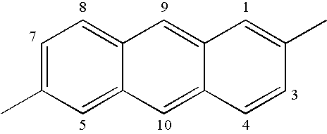
pentacene-2,9-diyl.
- Each Ac group has two covalently attached silylethynyl groups of formula —C≡C—Si(Ra)3. When the Ac group is derived from naphthalene, the two silylethynyl groups are typically attached to the same aromatic ring. When the Ac group is derived from anthracene or pentacene, the two silylethynyl groups can both be attached to the same inner aromatic ring or one silylethynyl group can be attached to each of the outer aromatic rings. As used herein, the term “inner aromatic ring” refers to an aromatic ring of an acene that is fused to two other aromatic rings. For example, the ring containing the 9 and 10 positions is referred to as the inner aromatic ring for an Ac group based on anthracene. As used herein, the term “outer aromatic ring” refers to an aromatic ring of an acene that is fused to only one aromatic ring. For example, the ring containing the 1, 2, 3, and 4 positions and the ring containing the 5, 6, 7, and 8 positions are referred to as the outer aromatic rings for an Ac group based on anthracene.
- In many embodiments, it is preferable that the silylethynyl groups are attached to an inner ring of the Ac group. For example, if the Ac group is derived from anthracene, the silylethynyl groups are preferably attached at the 9 and 10 positions. The stability of the acene precursor used to prepare the copolymers can often be improved by attachment of the silylethynyl groups to an inner aromatic ring of the Ac group. With multiple inner aromatic rings, attachment of the silylethynyl groups to the inner most ring, such as at the 6 and 13 positions of an Ac group derived from pentacene, may result in the greatest stability of the acene precursor. As used herein, stability refers to resistance to oxidation and/or dimerization.
- Each silylethynyl group is of formula —C≡C—Si—(Ra)3 where each Ra independently is hydrogen, alkyl, alkoxy, alkenyl, heteroalkyl, hydroxyalkyl, aryl, heteroaryl, aralkyl, or heteroaralkyl. Exemplary alkyl, alkoxy, alkenyl, heteroalkyl, and hydroxyalkyl groups can be linear, branched, cyclic, or a combination thereof and usually have up to 10 carbon atoms, up to 8 carbon atoms, up to 6 carbon atoms, or up to 4 carbon atoms. An exemplary aryl group is phenyl and an exemplary aralkyl is an alkyl having up to 10 carbon atoms that is substituted with a phenyl group. Exemplary heteroaryl groups often have a 5 or 6 membered unsaturated, heterocyclic ring that includes 1 or 2 heteroatoms and an exemplary heteroaralkyl is an alkyl having up to 10 carbon atoms that is substituted with a 5 or 6 membered heteroaryl having 1 or 2 heteroatoms.
- In more specific examples, each Ra is an alkyl having up to 10, up to 8, or up to 6, carbon atoms. That is, the silylethynyl group is a trialkylsilylethynyl group. Each alkyl group often has at least 1 carbon atom, at least 2 carbon atoms, or at least 3 carbon atoms. For example, in some copolymers of Formula I, the silylethynyl group is triisopropylsilylethynyl where Ra is isopropyl.
- In addition to the two silylethynyl groups, the Ac group can be optionally substituted with a substituent selected from an alkyl, alkoxy, thioalkyl, aryl, aralkyl, halo, haloalkyl, hydroxyalkyl, heteroalkyl, alkenyl, or combinations thereof When referring to Ac substituents, the term “combinations thereof” can refer either to multiple substituents on the Ac group or to a first substituent that is further substituted with a second substituent. At least in some embodiments, the addition of one or more substituents can increase the solubility of the copolymer of Formula I in organic solvents or can improve the compatibility of the copolymer with various coating compositions.
- Group Q can be attached to any position of Ac that lacks an attached silylethynyl group. The acene-thiophene copolymer of Formula I lacks a bithiophene or polythiophene group. That is, any two Ac(E)2 groups are separated by a group Q selected from a single group of Formula II to V. The copolymer is usually conjugated throughout the length of the copolymer. There are typically no spacer groups between two repeat units of formula —Ac(E)2—Q— in the copolymer that can disrupt the conjugation of double bonds along the backbone of the copolymer.
- In many embodiments, Q is attached to an outer aromatic ring of Ac. For example, group Q can be attached at positions 1, 2, 3, 4, 5, 6, 7, or 8 for an Ac group based on either naphthalene or anthracene and at positions 1, 2, 3, 4, 8, 9, 10, or 11 for an Ac group based on pentacene. When Q is attached to an outer aromatic ring of Ac and the Ac group is derived from anthracene or pentacene, the two silylethynyl groups are usually attached to an inner aromatic ring of Ac and preferably to the same inner aromatic ring.
- In other embodiments, Q is attached to an inner aromatic ring of Ac. For example, group Q can be attached at positions 9 or 10 for an Ac group based on anthracene or at
positions - In addition to being attached to group Q and to two silylethynyl, the Ac group is attached to a fourth group such as an end group of the copolymer or another repeat unit of formula —Ac(E)2—Q— where E refers to the silylethynyl groups (i.e., the resulting copolymeric material has a subscript n equal to at least 5). If group Q in Formula I is attached to an inner aromatic ring of the Ac group, the fourth group is often attached to the same inner aromatic ring. If group Q is attached to an outer aromatic ring of the Ac group, the fourth group is often attached to the opposite outer aromatic ring. That is, group Q and the fourth group are often attached to opposite distal ends of the Ac group with the two silylethynyl groups attached to an inner aromatic ring of the Ac group.
- Exemplary Ac(E)2 groups include, but are not limited to, 1,4-bis(silylethynyl)naphthalene-2,6-diyl, 1,4-bis(silylethynyl)naphthalene-2,7-diyl, 9,10-bis(silylethynyl)anthracene-2,6-diyl, 9,10-bis(silylethynyl)anthracene-2,7-diyl, 2,6-bis(silylethynyl)anthracene-9,10-diyl, 2,7-bis(silylethynyl)anthracene-9,10-diyl, 6,13-bis(silylethynyl)pentacene-2,9-diyl, 6,13-bis(silylethynyl)pentacene-2,10-diyl, 2,9-bis(silylethynyl)pentacene-6,13-diyl, or 2,10-bis(silylethynyl)pentacene-6,13-diyl. Any of these groups can optionally have the Ac group substituted with an alkyl, alkoxy, thioalkyl, aryl, aralkyl, halo, haloalkyl, hydroxyalkyl, heteroalkyl, alkenyl, or combinations thereof. The position numbers in front of the term “diyl” indicate the carbon atom where the Q group and the fourth group are attached to the Ac group.
- Some more specific Ac(E)2 groups include, but are not limited to, 1,4-bis(trialkylsilylethynyl)naphthalene-2,6-diyl, 1,4-bis(trialkylsilylethynyl)naphthalene-2,7-diyl, 9,10-bis(trialkylsilylethynyl)anthracene-2,6-diyl, 9,10-bis(trialkylsilylethynyl)anthracene-2,7-diyl, 2,6-bis(trialkylsilylethynyl)anthracene-9,10-diyl, 2,7-bis(trialkylsilylethynyl)anthracene-9,10-diyl, 6,13-bis(trialkylsilylethynyl)pentacene-2,9-diyl, 6,13-bis(trialkylsilylethynyl)pentacene-2,10-diyl, 2,9-bis(trialkylsilylethynyl)pentacene-6,13-diyl, or 2,10-bis(trialkylsilylethynyl)pentacene-6,13-diyl. Any of these groups can optionally have the Ac group substituted with an alkyl, alkoxy, thioalkyl, aryl, aralkyl, halo, haloalkyl, hydroxyalkyl, heteroalkyl, alkenyl, or combinations thereof The position numbers in front of the term “diyl” indicate the carbon atom where the Q group and the fourth group are attached to the Ac group.
- In some applications such as those in which the copolymers function as semiconductor materials, it may be desirable to select an Ac group that has an extended conjugation length in a linear direction (i.e., along the backbone of the copolymer). Such copolymers tend to align well with each other in the formation of stack-like structures. That is, in some applications, it is preferable that the Q group is attached to an outer aromatic ring of the acene with the two silylethynyl groups attached to an inner aromatic ring, if there is an inner aromatic ring. Exemplary Ac(E)2 groups include, but are not limited to, 1,4-bis(silylethynyl)naphthalene-2,6-diyl such as 1,4-bis(trialkylsilylethynyl)naphthalene-2,6-diyl, 9,10-bis(silylethynyl)anthracene-2,6-diyl such as 9,10-bis(trialkylsilylethynyl)anthracene-2,6-diyl, or 6,13-bis(silylethynyl)pentacene-2,9-diyl such as 6,13-bis(trialkylsilylethynyl)pentacene-2,9-diyl. Any of these groups can optionally have the Ac group substituted with an alkyl, alkoxy, thioalkyl, aryl, aralkyl, halo, haloalkyl, hydroxyalkyl, heteroalkyl, alkenyl, or combinations thereof.
- Group Q is selected from Formula II to V as described above. Each group R1 and R2 in these formulas is independently selected from hydrogen, alkyl, alkoxy, thioalkyl, aryl, aralkyl, halo, haloalkyl, hydroxyalkyl, heteroalkyl, alkenyl, or combinations thereof. When referring to groups R1 and R2, the term “combinations thereof” refers to a first group that is further substituted with another group.
- In some embodiments of group Q, there is at least one R1 group or R2 group that contains at least 4 carbon atoms such as 4 to 30 carbon atoms, 4 to 20 carbon atoms, 4 to 16 carbon atoms, or 4 to 10 carbon atoms. More specifically, there is at least one R1 group or R2 group selected from an alkyl having at least 4 carbon atoms, an alkoxy having at least 4 carbon atoms, a thioalkyl having at least 4 carbon atoms, an aryl having at least 6 carbon atoms, an aralkyl having at least 10 carbon atoms, a haloalkyl having at least 4 carbon atoms, a hydroxyalkyl having at least 4 carbon atoms, a heteroalkyl having at least 4 carbon atoms, an alkenyl having at least 4 carbon atoms, or combinations thereof The selection of at least one such group can often increase the solubility of the copolymer of Formula I in common organic solvents or can often improve the compatibility of the acene-thiophene copolymer with various coating compositions.
- Some exemplary copolymers have identical R1 and R2 groups selected from an alkyl having at least 4 carbon atoms, an alkoxy having at least 4 carbon atoms, a thioalkyl having at least 4 carbon atoms, an aryl having at least 6 carbon atoms, an aralkyl having at least 10 carbon atoms, a haloalkyl having at least 4 carbon atoms, a hydroxyalkyl having at least 4 carbon atoms, a heteroalkyl having at least 4 carbon atoms, an alkenyl having at least 4 carbon atoms, or a combination thereof.
- The copolymers of Formula I can be prepared using Suzuki coupling reactions such as shown in Reaction Scheme A.

A dihaloacene having two attached silylethynyl groups (i.e., Ac represents the acene group, E represents the group of formula —C—C—Si(Ra)3, and X represent a halo) is initially reacted with a dioxaborolane such as bis(pinacolato)diboron to form an acene compound having two dioxaborolane groups (e.g., tetramethyldioxaborolane). The resulting acene compound is then reacted with a dihalothiophene compound (i.e., X—Q—X) to form the copolymer of Formula I. The halo groups in the second reaction can be the same or different than the halo groups in the first reaction. Both of these reactions typically take place in the presence of a palladium catalyst such as, for example, [1,1′-bis(diphenylphosphino)ferrocene]dichloropalladium and tetrakis(triphenyl)phosphine)palladium(0). As an alternative to Reaction Scheme A, a dihalothiophene compound can be initially reacted with a dioxaborolane and then reacted using Suzuki coupling reactions with a dihaloacene having two attached silylethynyl groups. Suzuki coupling reactions are further described in the article by Ito et al., Angew. Chem., Int. Ed., 42, 1159-1162 (2003) and supporting information referenced therein. - Stille coupling reactions can also be used to synthesize the copolymers of Formula I as shown in Reaction Scheme B.

A thiophene compound can be lithiated and then reacted with a trialkylstannate such as tributyltin chloride to form a thiophene compound substituted with two trialkylstannate groups. The resulting thiophene compound can then be reacted in the presence of a palladium catalyst with a dihaloacene having two attached silylethynyl groups. As an alternative to Reaction Scheme B, an acene with two attached silylethynyl groups can be lithiated and then reacted with a trialkylstannate to form an acene substituted with two trialkylstannate groups. The resulting acene compound can then be reacted with a dihalothiophene in the presence of a palladium catalyst. Stille coupling reactions are further described in the articles Miller et al., J. Org. Chem., 60, 6813-6819 (1995) and Katz et al., Acc. Chem. Res., 34, 359-369 (2001). - Dihaloacenes having two silylethynyl groups can be synthesized from a dihaloacene as shown in the Example Section or as shown in Reaction Scheme C. For example, 1,4-bis(silylethynyl)-2,6-dihalonaphthalene can be synthesized starting with 2,6-dihalonaphthlene such as 2,6-dichloronaphthalene, which is commercially available from Apin Chemicals Ltd., Oxfordshire, UK.

The 2,6-dihalonaphthalene can be oxidized to 2,6-dihalonaphthaquinone. The silylethynyl groups can be added by formation of a lithiated version of silylacetylene compounds followed by reaction with the 2,6-dihalonaphthaquinone. Various silylacetylene compounds are commercially available. For example, (trimethylsilyl)acetylene, (triethylsilyl)acetylene, (triisopropylsilyl)acetylene, and (tert-butyldimethylsilyl)acetylene are available from GFS Chemicals, Columbus, Ohio. (Dimethylphenylsilyl)acetylene, (methyldiphenylsilyl)acetylene, and (triphenylsilyl)acetylene are available from Aldrich Chemical Co., Milwaukee, Wis. The resulting diol product can then be converted to the corresponding aromatic compound by reaction with a reducing agent such as stannous chloride. - Dihalopentacenes with the halo group in the 2,9 or 2,10 positions can be synthesized as shown in Reaction Scheme D. The reaction of a halobenzene with pyromellitic anhydride under typical Friedel-Crafts conditions (e.g., AlCl3, which is a strong Lewis Acid) in an inert solvent or with halobenzene as solvent with heat gives the two isomeric bis(halobenzoyl)phthalic acids A and B. These isomers can be separated by fractional recrystallization, chromatography or by differences in solubility. Further reactions of the individual bis(halobenzoyl)phthalic acids A and B are carried on separately first by cyclization to the corresponding tetrones C and D using triflic acid followed by reduction to the desired pentacenes E and F with sodium borohydride and stannous chloride. The R3 groups below are hydrogen or substituent groups.


The resulting dihalopentacenes can be reacted to attach two silylethynyl groups using a method analogous to that shown in Reaction Scheme C. Oxidation of compounds E and F would give the corresponding quinones G and H respectively. These compounds compounds could then be converted to derivatives with the silylethynyl groups attached at the 6 and 13 positions of the pentacene.
- Dibromothiophene compounds of Formula IIa

can be prepared by bromination of the corresponding thiophene compound. That is, the corresponding thiophene can be reacted with a brominating agent such as N-bromosuccinimide (NBS). For example, a compound of Formula Ia with R1 and R2 equal to alkyl groups can be prepared by reacting a 3,4-dihalothiophene with two moles of a Grignard reagent containing the desired alkyl groups followed by a bromination reaction. This method is further described in the article by Vidal et al., Chem. Eur. J., 6, 1663-1673 (2000). - Dihalothieno[3,2-b]thiophenes of Formula IIa

can be prepared by bromination of the corresponding thieno[3,2-b]thiophenes. Some thieno[3,2-b]thiophenes are commercially available from Maybridge, Cornwall, UK. 3,6-dimethylthieno[3,2-b]thiophene is available from Synchem OHG, Kassel, Germany and 2,5-dibromothieno[3,2-b]thiophene is available from Aldrich, Milwaukee, Wis. Other thieno[3,2-b]thiophenes can be synthesized as described in the article by Zhang et al., Macromolecules, 37, 6306-6315 (2004). - Dihalothieno[2,3-b]thiophenes of Formula IVa

can be prepared by bromination of the corresponding thieno[2,3-b]thiophenes. 3,4-dimethylthieno[2,3-b]thiophene is commercially available from Alfa Aesar Johnson Mathey, Ward Hill, Mass. Other substituted thieno[2,3-b]thiophenes can be prepared using an analogous reaction to that described in the article by Comel et. al, Journal of Heterocyclic Chemistry, 38, 1167-1171 (2001). - Likewise, dihaloethylenedioxythiophene compounds of Formula Va

can be prepared by bromination of the corresponding ethylenedioxythiophenes. The corresponding ethylenedioxythiophenes can be prepared, for example, by transesterificative cyclocondensation of commercially available 3,4-dimethoxythiophenes with geminal diols such as 2,3-butanediol, 1,2-propanediol, and the like in the presence of an acid catalyst such as p-toluenesulfonic acid. The resulting 3,4-disubstituted thiophene can then be dibrominated at the 2 and 5 positions with N-bromosuccinimide or other suitable brominating agents. This method is further described in the article by Nielson et al, Macromolecules, 38, 10379 (2005). - The copolymers of Formula I typically have a weight average molecular weight of at least 5,000 g/mole. In some embodiments, the weight average molecular weight is at least 7,000 g/mole, at least 8,000 g/mole, at least 10,000 g/mole, at least 12,000 g/mole, or at least 15,000 g/mole. The weight average molecular weight can be determined using Gel Permeation Chromatography.
- If desired, the purity of the copolymeric material can be increased using techniques known in the art such as additional precipitation steps or Soxhlet extraction.
- Layers in an electronic device that contain the acene-thiophene copolymer of Formula I often are prepared from solvent-based compositions. That is, at least some of the acene-thiophene copolymers of Formula I are soluble in a solvent. Suitable solvents for dissolution of the copolymer of Formula I include, but are not limited to, aromatic solvents such as toluene, benzene, and xylene; ethers such as tetrahydrofuran and dioxane; ketones such as methyl isobutyl ketone and methyl ethyl ketone; chlorinated solvents such as chloroform, dichloromethane, chlorobenzene, and dichlorobenzene; alkanes such as cyclohexane and heptane; and amides such as N,N-dimethylformamide and 1-methylpyrrolidone. As used herein, the term “soluble” means the copolymer can be dissolved in a solvent to provide a solution that contains at least 0.05 weight percent copolymer based on the weight of the solution. Some copolymers have a solubility of at least 0.05 weight percent, at least 0.1 weight percent, at least 0.2 weight percent, at least 0.5 weight percent, at least 1 weight percent, at least 2 weight percent, at least 3 weight percent, or at least 5 weight percent based on the weight of the solution.
- Compositions that contain the acene-thiophene copolymer and a solvent can be used to provide a coating. The coating can be formed by applying the compositions to a surface such as to a surface of a substrate or to a surface of another layer in an electronic device. The coating can be applied using any suitable application technique such as, for example, spray coating, spin coating, dip coating, knife coating, gravure coating, inkjet printing, and transfer printing. The solvent can be removed from the coating after application by evaporating under ambient conditions (e.g., at about 20° C. to about 25° C.) or by drying at an elevated temperature such as a temperature up to about 80° C., up to about 100° C., up to about 120° C., up to about 150° C., or up to about 200° C.
- In some exemplary methods of preparing an electronic device, the method involves providing a first layer selected from a dielectric layer, a conductive layer, or a substrate and disposing a layer containing the acene-thiophene copolymer of Formula I adjacent to the first layer. No specific order of preparing or providing is necessary; however, the layer containing the acene-thiophene copolymer is often prepared on the surface of another layer such as the dielectric layer, the conductive layer, or the substrate. The conductive layer can include, for example, a source electrode and a drain electrode, an anode, or a cathode.
- As used herein, the terms “disposed”, “disposing”, “deposited”, “depositing”, and “adjacent” do not preclude the presence of another layer or layers between the mentioned layers. As used herein, these terms mean that a first layer is positioned near a second layer. The first layer often contacts the second layer but a third layer or layers could be positioned between the first layer and the second layer.
- The acene-thiophene copolymers of Formula I can function as semiconductor materials within some electronic devices. That is, the electronic device can be a semiconductor device that contains a semiconductor layer that includes the acene-thiophene copolymer of Formula I. Semiconductor devices have been described, for example, by S. M. Sze in Physics of Semiconductor Devices, 2nd edition, John Wiley and Sons, N.Y. (1981). Such devices include rectifiers, transistors (of which there are many types, including p-n-p, n-p-n, and thin-film transistors), photoconductors, current limiters, thermistors, p-n junctions, field-effect diodes, Schottky diodes, and the like. Semiconductor devices can include components such as transistors, arrays of transistors, diodes, capacitors, embedded capacitors, and resistors that are used to form circuits. Semiconductor devices also can include arrays of circuits that perform an electronic function. Examples of these arrays or integrated circuits include inverters, oscillators, shift registers, and logic circuits. Applications of these semiconductor devices and arrays include radio frequency identification devices (RFIDs), smart cards, display backplanes, sensors, memory devices, and the like.
- Some of the semiconductor devices are organic thin-film transistors as shown schematically in FIGS. 1 to 6. Any given layer in the various thin film transistors shown in FIGS. 1 to 6 can include multiple layers of materials. Further, any layer can include a single material or multiple materials.
- One embodiment of an organic thin-
film transistor 100 is shown schematically inFIG. 1 . The organic thin-film transistor (OTFT) 100 includes agate electrode 14, agate dielectric layer 16 disposed on thegate electrode 14, asource electrode 22, adrain electrode 24, and asemiconductor layer 20 that is in contact with both thesource electrode 22 and thedrain electrode 24. Thesource electrode 22 and thedrain electrode 24 are separated from each other (i.e., thesource electrode 22 does not contact the drain electrode 24) and are positioned adjacent to thedielectric layer 16. Both thesource electrode 22 and thedrain electrode 24 are in contact with thesemiconducting layer 20 such that a portion of the semiconductor layer is positioned between the source electrode and the drain electrode. The portion of the semiconductor layer that is positioned between the source electrode and the drain electrode is referred to as thechannel 21. The channel is adjacent to thegate dielectric layer 16. Some semiconductor devices have an optional surface treatment layer between thegate dielectric layer 16 and thesemiconductor layer 20. - An optional substrate can be included in the organic thin-film transistors. For example, the
optional substrate 12 can be adjacent to thegate electrode 14 as shown schematically inFIG. 2 for theOTFT 200 or adjacent to thesemiconductor layer 20 as shown schematically inFIG. 3 for theOTFT 300. TheOTFT 300 can include an optional surface treatment layer between thesubstrate 12 and thesemiconductor layer 20. - Another embodiment of an organic thin-film transistor is shown schematically in
FIG. 4 . This organic thin-film transistor 400 includes agate electrode 14, agate dielectric layer 16 disposed on thegate electrode 14, asemiconductor layer 20, and asource electrode 22 and adrain electrode 24 disposed on thesemiconductor layer 20. In this embodiment, thesemiconductor layer 20 is between thegate dielectric layer 16 and both thesource electrode 22 and thedrain electrode 24. Thesource electrode 22 and thedrain electrode 24 are separated from each other (i.e., thesource electrode 22 does not contact the drain electrode 24). Both thesource electrode 22 and thedrain electrode 24 are in contact with the semiconducting layer such that a portion of the semiconductor layer is positioned between the source electrode and the drain electrode. Thechanel 21 is the portion of the semiconductor layer that is positioned between thesource electrode 22 and thedrain electrode 24. One or more optional surface treatment layers can be included in the semiconductor device. For example, an optional surface treatment layer can be included between thegate dielectric layer 16 and thesemiconductor layer 20. - An optional substrate can be included in the organic thin-film transistors. For example, the
optional substrate 12 can be in contact with thegate electrode 14 as shown schematically inFIG. 5 for theOTFT 500 or in contact with thesemiconductor layer 20 as shown schematically inFIG. 6 for theOTFT 600.OTFT 600 can include an optional surface treatment layer between thesubstrate 12 and thesemiconductor layer 20. - In operation of the semiconductor device configurations shown in FIGS. 1 to 6, voltage can be applied to the
drain electrode 24. However, at least ideally, no charge (i.e., current) is passed to thesource electrode 22 unless voltage is also applied to thegate electrode 14. That is, unless voltage is applied to thegate electrode 14, thechanel 21 in thesemiconductor layer 20 remains in a non-conductive state. Upon application of voltage to thegate electrode 14, thechanel 21 becomes conductive and charge flows through thechanel 21 from thesource electrode 22 to thedrain electrode 24. - A
substrate 12 often supports the OTFT during manufacturing, testing, and/or use. Optionally, the substrate can provide an electrical function for the OTFT. For example, the backside of the substrate can provide electrical contact. Useful substrate materials include, but are not limited to, inorganic glasses, ceramic materials, polymeric materials, filled polymeric materials (e.g., fiber-reinforced polymeric materials), metals, paper, woven or non-woven cloth, coated or uncoated metallic foils, or a combination thereof. - The
gate electrode 14 can include one or more layers of a conductive material. For example, the gate electrode can include a doped silicon material, a metal, an alloy, a conductive polymer, or a combination thereof. Suitable metals and alloys include, but are not limited to, aluminum, chromium, gold, silver, nickel, palladium, platinum, tantalum, titanium, indium tin oxide (ITO), fluorine tin oxide (FTO), antimony doped tin oxide (ATO), or a combination thereof Exemplary conductive polymers include, but are not limited to, polyaniline, poly(3,4-ethylenedioxythiophene)/poly(styrene sulfonate), or polypyrrole. In some organic thin film transistors, the same material can provide both the gate electrode function and the support function of the substrate. For example, doped silicon can function as both the gate electrode and as the substrate. - The gate electrode in some embodiments is formed by coating a substrate surface with a dispersion that contains conductive materials such as nanoparticles that are conductive or polymeric materials that are conductive. Conductive nanoparticles include, but are not limited to, ITO nanoparticles, ATO nanoparticles, silver nanoparticles, gold nanoparticles, or carbon nanotubes.
- The
gate dielectric layer 16 is disposed on thegate electrode 14. This gatedielectric layer 16 electrically insulates thegate electrode 14 from the balance of the OTFT device. Useful materials for the gate dielectric include, for example, an inorganic dielectric material, a polymeric dielectric material, or a combination thereof The gate dielectric can be a single layer or multiple layers of suitable dielectric materials. Each layer in a single or multilayer dielectric can include one or more dielectric materials. - The organic thin film transistors can include an optional surface treatment layer disposed between the
gate dielectric layer 16 and at least a portion of theorganic semiconductor layer 20 or disposed between thesubstrate 12 and at least a portion of theorganic semiconductor layer 20. In some embodiments, the optional surface treatment layer serves as an interface between the gate dielectric layer and the semiconductor layer or between the substrate and the semiconductor layer. The surface treatment layer can be a self-assembled monolayer as described in U.S. Pat. No. 6,433,359 B1 (Kelley et al.) or a polymeric material as described in U.S. Patent Application Publication 2003/0102471 A1 (Kelley et al.) and U.S. Pat. No. 6,617,609 (Kelley et al.). - The
source electrode 22 anddrain electrode 24 can be metals, alloys, metallic compounds, conductive metal oxides, conductive ceramics, conductive dispersions, and conductive polymers, including, for example, gold, silver, nickel, chromium, barium, platinum, palladium, aluminum, calcium, titanium, indium tin oxide (ITO), fluorine tin oxide (FTO), antimony tin oxide (ATO), indium zinc oxide (IZO), poly(3,4-ethylenedioxythiophene)/poly(styrene sulfonate), polyaniline, other conducting polymers, alloys thereof, combinations thereof, and multiple layers thereof Some of these materials are appropriate for use with n-type semiconductor materials and others are appropriate for use with p-type semiconductor materials, as is known in the art. - The organic thin film transistors exemplified in FIGS. 1 to 3 can be prepared by a method that involves arranging multiple layers in the following order: a gate electrode; a gate dielectric layer; a layer having a source electrode and a drain electrode that are separated from each other; and a semiconductor layer in contact with both the source electrode and the drain electrode. The semiconductor layer includes an acene-thiophene copolymer of Formula I.
- For example, the organic thin film transistor shown schematically in
FIG. 1 can be prepared by providing agate electrode 14; depositing agate dielectric layer 16 adjacent to thegate electrode 14; positioning asource electrode 22 and adrain electrode 24 adjacent to thegate dielectric layer 16 such that thesource electrode 22 and thedrain electrode 24 are separated from each other; and forming asemiconductor layer 20 that is deposited on thesource electrode 22, on thedrain electrode 24, and in thearea 21 between thesource electrode 22 and thedrain electrode 24. Thesemiconductor layer 20 contacts both thesource electrode 22 and thedrain electrode 24. The portion of the semiconductor layer that is positioned in the area between the source electrode and the drain electrode defines a channel. - The organic thin film transistor shown schematically in
FIG. 2 can be prepared by providing asubstrate 12; depositing agate electrode 14 on thesubstrate 12; depositing agate dielectric layer 16 adjacent to thegate electrode 14 such that thegate electrode 14 is positioned between thesubstrate 12 and thegate dielectric layer 16; positioning asource electrode 22 and adrain electrode 24 adjacent to thegate dielectric layer 16 such that the two electrodes are separated from each other; and forming asemiconductor layer 20 adjacent to thesource electrode 22, thedrain electrode 24, and in thearea 21 between thesource electrode 22 and thedrain electrode 24. Thesemiconductor layer 20 contacts both thesource electrode 22 and thedrain electrode 24. The portion of the semiconductor layer that is positioned in the area between the source electrode and the drain electrode defines a channel. - The organic thin film transistor shown schematically in
FIG. 3 can be prepared by providing asubstrate 12; forming asemiconductor layer 20 adjacent to thesubstrate 12; positioning asource electrode 22 and adrain electrode 24 adjacent to thesemiconductor layer 20 opposite thesubstrate 12 such that thesource electrode 22 anddrain electrodes 24 are separated from each other; depositing agate dielectric layer 16 adjacent to thesource electrode 22, thedrain electrode 24, and a portion of thesemiconducting layer 20 between thesource electrode 22 and thedrain electrode 24; and depositing agate electrode 14 adjacent to thegate dielectric layer 16. Both thesource electrode 22 and thedrain electrode 24 contact thesemiconductor layer 20. A portion of the semiconductor layer is positioned between thesource electrode 22 and thedrain electrode 24. This portion of the semiconductor layer defines a channel. - The organic thin film transistors shown schematically in FIGS. 4 to 6 can be prepared by a method that involves arranging multiple layers in the following order: a gate electrode; a gate dielectric layer; a semiconductor layer containing the acene-thiophene copolymer of Formula I; and a layer having a source electrode and a drain electrode that are separated from each other, wherein the semiconductor layer contacts both the drain electrode and the source electrode. In some embodiments, a surface treatment layer can be positioned between the gate dielectric layer and the semiconductor layer. A substrate can be positioned adjacent to the gate electrode or adjacent to the layer containing the source electrode and the drain electrode.
- For example, the organic thin film transistor shown schematically in
FIG. 4 can be prepared by providing agate electrode 14; depositing agate dielectric layer 16 adjacent to thegate electrode 14; forming asemiconductor layer 20 adjacent to the gate dielectric layer 16 (i.e., thegate dielectric layer 16 is positioned between thegate electrode 14 and the semiconducting layer 20); and positioning asource electrode 22 and adrain electrode 24 adjacent to thesemiconductor layer 20. Thesource electrode 22 and thedrain electrode 24 are separated from each other and both electrodes are in contact with thesemiconductor layer 20. A portion of the semiconductor layer is positioned between the source and drain electrodes. - The organic thin film transistor shown schematically in
FIG. 5 can be prepared by providing asubstrate 12, depositing agate electrode 14 adjacent to thesubstrate 12, depositing agate dielectric layer 16 adjacent to thegate electrode 14 such that thegate electrode 14 is positioned between thesubstrate 12 and thegate dielectric layer 16; forming asemiconductor layer 20 adjacent to thegate dielectric layer 16; and positioning asource electrode 22 and adrain electrode 24 adjacent to thesemiconductor layer 20. Thesource electrode 22 and thedrain electrode 24 are separated from each other and both electrodes are in contact with thesemiconductor layer 20. A portion of thesemiconductor layer 20 is positioned between thesource electrode 22 and thedrain electrode 24. - The organic thin film transistor shown schematically in
FIG. 6 can be prepared by providing asubstrate 12; positioning asource electrode 22 and adrain electrode 24 adjacent to the substrate such that thesource electrode 22 and thedrain electrode 24 are separated from each other; forming asemiconductor layer 20 that contacts thesource electrode 22 and thedrain electrode 24; and depositing agate dielectric layer 16 adjacent to the semiconductor layer opposite thesource electrode 22 and thedrain electrode 24; and depositing agate electrode 14 adjacent to thegate dielectric layer 16. A portion of thesemiconductor layer 20 is positioned between thesource electrode 22 and thedrain electrode 24. - The acene-thiophene copolymers of Formula I can be used in other types of electronic devices such as electronic devices in which the copolymer is positioned in a layer between a first electrode (e.g., anode) and a second electrode (e.g., cathode). Exemplary electronic devices include, but are not limited to, organic photovoltaic cells and organic electroluminescent devices such as organic light emitting diodes.
- Organic photovoltaic cells and organic electroluminescent devices include many common components such as an anode, a cathode, and a material positioned between the anode and cathode. However, the operational concepts of these two types of devices are reversed. In an organic electroluminescent device, light is emitted as the result of charge transport between the two electrodes. An electron is introduced at a first electrode having a low work function (i.e., the cathode) and a hole is introduced at a second electrode having a high work function (i.e., the anode). In the organic emissive element positioned between the two electrodes, the electron and hole recombine and emit light. Conversely, in a photovoltaic cell, charge transport between the two electrodes results from the exposure of the active layer to light. The active layer, which is positioned between two electrodes, adsorbs light that passes through one of the electrodes. The absorption of light causes the formation of an exiton (i.e., an excited electron-hole pair) that is subsequently dissociated into an electron and a hole that migrate towards opposite electrodes.
- Organic electroluminescent (OEL) devices such as organic light emitting diodes include an organic emissive element positioned between two electrodes (i.e., an anode and a cathode). The organic emissive element of an organic electroluminescent device usually includes at least one light emitting layer that includes an electroluminescent material. Other layers can also be present in the organic emissive element such as a hole transport layers, electron transport layer, hole injection layer, electron injection layer, hole blocking layer, electron blocking layer, buffer layer, and the like. In addition, photoluminescent materials can be present in the light emitting layer or other layers in the organic emissive element, for example, to convert the color of light emitted by the electroluminescent material to another color. These and other such layers and materials can be used to alter or tune the electronic properties and behavior of the layered OEL device. For example, the additional layers can be used to achieve a desired current/voltage response, a desired device efficiency, a desired color, a desired brightness, and the like.
-
FIGS. 7A to 7D illustrate examples of different OEL device (for example, an organic light emitting diode) configurations. Each configuration includes asubstrate 30, ananode 32, acathode 34, and alight emitting layer 36. The configurations ofFIGS. 7C and 7D also include ahole transport layer 38 and the configurations ofFIGS. 7B and 7D include anelectron transport layer 40. The layer or layers positioned between the two electrodes conduct holes from the anode or electrons from the cathode, respectively. The acene-thiophene copolymer can be in a light emitting layer, a hole transport layer, or a combination thereof. Within any layer, the acene-thiophene copolymer may be present alone or in combination with other materials. - In some organic emissive elements, the acene-thiophene copolymer is present in a light emitting layer. The acene-thiophene copolymer can be used alone or in combination with one or more materials in the light emitting layer. For example, the copolymers can function as a host material or as a dopant material within a light emitting layer.
- As used herein, the term “dopant” refers to a material that is capable of being excited by a transfer of energy from a host material. The excited dopant emits light. The dopant is typically present in an amount less than 50 weight percent, less than 40 weight percent, less than 20 weight percent, less than 10 weight percent, or less than 5 weight percent based on the weight of material in the light emitting layer. The dopant is typically present in an amount of at least 0.1 weight percent, 0.2 weight percent, 0.5 weight percent, or 1 weight percent based on the weight of material in the light emitting layer.
- When the acene-thiophene copolymer is used as a dopant in the light emitting layer, it can be combined with host materials such as, for example, a charge transfer material. The charge transfer material is often a hole transfer material such as a diamine derivative, a triarylamine derivative, or a combination thereof. Exemplary diamine derivatives include, but are not limited to, N,N′-bis(3-methylphenyl)-N,N′-bis(phenyl)benzidine (TPD), N,N′-bis(2-naphthyl)-N,N′-bis(phenyl)benzidine (beta-NPB), and N,N′-bis(1-naphthyl)-N,N′-bis(phenyl)benzidine (NPB). Exemplary triarylamine derivative include, but are not limited to, 4,4′,4″-Tris(N,N -diphenylamino)triphenylamine (TDATA) and 4,4′,4″-Tris(N-3-methylphenyl-N -phenylamino)triphenylamine (MTDATA). Still other host materials include electron transfer materials such as, for example, 9,10-di(2-naphthyl)anthracene (ADN) and oxadiazole compounds such as 1,3-bis[5-(4-(1,1-dimethylethyl)phenyl)-1,3,4-oxadiazol-2-yl]benzene and 2-(biphenyl-4-yl)-5-(4-(1,1-dimethylethyl)phenyl)-1,3,4-oxadiazole.
- As used herein, the term “host” refers to a material that is capable of transferring energy to a dopant to form an excited dopant that emits light. The host material is typically present in an amount of at least at least 50 weight percent, at least 60 weight percent, at least 80 weight percent, or at least 90 weight percent based on the weight of material in the light emitting layer.
- When the light emitting layer contains a host material and a dopant, the excited state of the host material is typically at a higher energy level than the excited state of the dopant so that energy can be transferred from the host material to the dopant. The excited host material typically emits light of a shorter wavelength than the excited dopant. For example, host material that emits blue light can transfer energy to a dopant that emits green or red light and a host material that emits green light can transfer energy to a dopant that emits red light but not to a dopant that emits blue light.
- When the acene-thiophene copolymer is present in a light emitting layer of an organic emissive element, other light emitting materials can be present in the same light emitting layer or in different light emitting layers. Some light emitting layers have a small molecule (SM) emitter, a small molecule emitter doped polymer, a light emitting polymer (LEP), a small molecule emitter doped light emitting polymer, a blend of light emitting polymers, or a combination thereof. The emitted light from the organic emissive element can be in any portion of the visible spectrum depending on the composition of the electroluminescent composition in the light emitting layer or layers.
- Suitable LEP materials are typically conjugated polymeric or oligomeric molecules that preferably have sufficient film-forming properties for solution processing. As used herein, “conjugated polymers or oligomeric molecules” refer to polymers or oligomers having a delocalized π-electron system along the polymer backbone. Such polymers or oligomers are semiconducting and can support positive or negative charge carriers along the polymeric or oligomeric chain.
- Exemplary LEP materials include poly(phenylenevinylenes), poly(para-phenylenes), polyfluorenes, other LEP materials now known or later developed, and co-polymers or blends thereof Suitable LEPs can also be doped with a small molecule emitter, dispersed with fluorescent dyes or photoluminescent materials, blended with active or non-active materials, dispersed with active or non-active materials, and the like. Examples of suitable LEP materials are further described in Kraft, et al., Angew. Chem. Int. Ed., 37, 402-428 (1998); U.S. Pat. Nos. 5,621,131; 5,708,130; 5,728,801; 5,840,217; 5,869,350; 5,900,327; 5,929,194; 6,132,641; and 6,169,163; and PCT Patent Application Publication No. 99/40655.
- LEP materials can be formed into a light emitting structure, for example, by casting a solvent solution of the LEP material on a substrate and evaporating the solvent to produce a polymeric film. Alternatively, LEP material can be formed in situ on a substrate by reaction of precursor species. Suitable methods of forming LEP layers are described in U.S. Pat. No. 5,408,109. Other methods of forming a light emitting structure from LEP materials include, but are not limited to, laser thermal patterning, inkjet printing, screen printing, thermal head printing, photolithographic patterning, spraying, and extrusion coating.
- Suitable SM electroluminescent materials include charge transporting, charge blocking, and semiconducting organic or organometallic compounds. Typically, SM materials can be vacuum deposited or coated from solution to form thin layers in a device. In practice, multiple layers of SM materials are typically used to produce efficient organic electroluminescent devices since a given material generally does not have both the desired charge transport and electroluminescent properties.
- Exemplary SM materials include N,N′-bis(3-methylphenyl)-N,N′-diphenylbenzidine (TPD) and metal chelate compounds such as tris(8-hydroxyquinoline) aluminum (Alq3). Other SM materials are disclosed in, for example, C.H. Chen, et al., Macromol. Symp. 125, 1 (1997); Japanese Laid Open Patent Application 2000-195673; U.S. Pat. Nos. 6,030,715; 6,150,043; and 6,242,115; and PCT Patent Applications Publication Nos. WO 00/18851 (divalent lanthanide metal complexes), WO 00/70655 (cyclometallated iridium compounds and others), and WO 98/55561.
- The
anode 32 andcathode 34 are typically formed using conducting materials such as metals, alloys, metallic compounds, conductive metal oxides, conductive ceramics, conductive dispersions, and conductive polymers, including, for example, gold, silver, nickel, chromium, barium, platinum, palladium, aluminum, calcium, titanium, indium tin oxide (ITO), fluorine tin oxide (FTO), antimony tin oxide (ATO), indium zinc oxide (IZO), poly(3,4-ethylenedioxythiophene)/poly(styrene sulfonate), polyaniline, other conducting polymers, alloys thereof, combinations thereof, and multiple layers thereof. Theanode 32 and thecathode 34 can be single layers of conducting materials or they can include multiple layers. For example, an anode or a cathode may include a layer of aluminum and a layer of gold, a layer of calcium and a layer of aluminum, a layer of aluminum and a layer of lithium fluoride, or a metal layer and a conductive organic layer. - A typical anode for an organic electroluminescent device is indium-tin-oxide (ITO) sputtered onto a transparent substrate such as plastic or glass. Suitable substrates include, for example, glass, transparent plastics such as polyolefins, polyethersulfones, polycarbonates, polyesters such as polyethylene naphthalate (PEN), polyarylates, and polymeric multilayer films, ITO coated barrier films such as the Plastic Film Conductor available from 3M (St. Paul, Minn.), surface-treated films, and selected polyimides.
- The anode material coating the substrate is electrically conductive and may be optically transparent or semi-transparent. In addition to ITO, suitable anode materials include indium oxide, fluorine tin oxide (FTO), zinc oxide, vanadium oxide, zinc-tin oxide, gold, platinum, palladium, other high work function metals, and combinations thereof.
- Optionally, the anode can be coated with a buffer layer to help provide a flat surface and to modify the effective work function of the anode. The buffer layer typically has a thickness up to 5000 Angstroms, up to 4000 Angstroms, up to 3000 Angstroms, up to 1000 Angstroms, up to 800 Angstroms, up to 600 Angstroms, up to 400 Angstroms, or up to 200 Angstroms. The buffer layer often has a thickness of at least 5 Angstroms, at least 10 Angstroms, or at least 20 Angstroms. The buffer layer can be vapor coated or solution coated.
- Suitable buffer layers can be an ionic polymer such as poly(3,4-oxyethyleneoxy thiophene)/poly(styrene sulfonate), polyaniline emeraldine, or an acid doped polypyrrole. Other suitable buffer layers include those described in U.S. Patent Application Ser. No. 2004/0004433A1, incorporated herein by reference, that include (a) a hole transport material having triarylamine moieties and (b) an electron acceptor material. Suitable hole transport material can be a small molecule or a polymeric material. Exemplary hole transport material include, but are not limited to, 4,4′,4″-tris(N,N -diphenylamino)triphenylamine (TDATA), 4,4″,4″-tris(N-3-methylphenyl-N -phenylamino)triphenylamine (MTDAA), 4,4′,4″-tris(carbozole-9-yl)triphenylamine (TCTA), and 4,4′,4″-tris(N-naphthyl)-N-phenylamino)triphenylamine (2-TNATA). Exemplary electron transport materials that can be included in such a buffer layer include, but are not limited to, tetracyanoquinodimethane (TCNQ), tetafluoro-tetracynaoquinodimethan, tetracyanoethylene, chloranil, 2-(4-(1-methylethyl)phenyl-6-phenyl-4H-thiopyran-4-ylidene)-propanedinitrile-1,1-dioxyide (PTYPD), and 2,4,7-trinitrofluorene.
- Typical cathodes include low work function metals such as aluminum, barium, calcium, samarium, magnesium, silver, magnesium/silver alloys, lithium, lithium fluoride, ytterbium, and of calcium/magnesium alloys. The cathode can be a single layer or multiple layers of these materials. For example, the cathode can include a layer of lithium fluoride, a layer of aluminum, and a layer of silver.
- The
hole transport layer 38 facilitates the injection of holes from the anode into the device and their migration towards the recombination zone. Thehole transport layer 38 can further act as a barrier for the passage of electrons to theanode 32. In some examples, the acene-thiophene copolymer can be used in the hole transport layer. In other examples, thehole transport layer 38 can include, for example, a diamine derivative, such as N,N′-bis(3-methylphenyl)-N,N′-bis(phenyl)benzidine (TPD), N,N′-bis(2-naphthyl)-N,N′-bis(phenyl)benzidine (beta-NPB), and N,N′-bis(1-naphthyl)-N,N′-bis(phenyl)benzidine (NPB); or a triarylamine derivative, such as, 4,4′,4″-tris(N,N -diphenylamino)triphenylamine (TDATA), 4,4′,4″-tris(N-3-methylphenyl-N -phenylamino)triphenylamine (MTDATA), 4,4′,4″-tri(N-phenoxazinyl) triphenylamine (TPOTA), and 1,3,5-tris(4-diphenylaminophenyl)benzene (TDAPB). - The
electron transport layer 40 facilitates the injection of electrons from the cathode into the device and their migration towards the recombination zone. Theelectron transport layer 40 can further act as a barrier for the passage of holes to thecathode 34. In some examples, theelectron transport layer 40 can be formed using the organometallic compound such as tris(8-hydroxyquinolato) aluminum (Alq3) and biphenylato bis(8-hydroxyquinolato)aluminum (BAlq). Other examples of electron transport materials useful in electron transport layer 260 include 1,3-bis[5-(4-(1,1-dimethylethyl)phenyl)-1,3,4-oxadiazol-2-yl]benzene; 2-(biphenyl-4-yl)-5-(4-(1,1-dimethylethyl)phenyl)-1,3,4-oxadiazole 9,10-di(2-naphthyl)anthracene (ADN); 2-(4-biphenyl)-5-(4-t-butylphenyl) -1,3,4-oxadiazole; or 3-(4-biphenylyl)-4-phenyl-5-(4-tert-butylphenyl)-1,2,4-triazole (TAZ). - Other layers such as, for example, additional hole injection layers containing, for example, porphyrinic compounds like copper phthalocyanine (CuPc) and zinc phthalocyanine; electron injection layers containing, for example, alkaline metal oxides or alkaline metal salts; hole blocking layers containing, for example, molecular oxadiazole and triazole derivatives such as 2-(4-biphenyl)-5-(4-t-butylphenyl)-1,3,4-oxadiazole (PBD), 2,9-dimethyl-4,7-diphenyl-1,10-phenanthraline (BCP), biphenylato bis(8-hydroxyquinolato)aluminum (BAlq), or 3-(4-biphenylyl)-4-phenyl-5-(4-tert-butylphenyl)-1,2,4-triazole (TAZ); electron blocking layers containing, for example, N,N′-bis(1-naphthyl)-N,N′-bis(phenyl) benzidine (NPB), or 4,4′,4″-tris(N-(3-methylphenyl)-N -phenylamino)triphenylamine (MTDATA); or the like can also be present in organic emissive element. In addition, photoluminescent materials can be present in these layers, for example, to convert the color of light emitted by the electroluminescent material to another color. These and other such layers and materials can be used to alter or tune the electronic properties and behavior of the layered OEL device, for example, to achieve one or more features such as a desired current/voltage response, a desired device efficiency, a desired color, a desired brightness, a desired device lifetime, or a desired combination of these features.
-
FIG. 8 schematically illustrates an exemplary photovoltaic cell, which is another type of electronic device that can contain the acene-thiophene copolymer of Formula I. Anactive layer 54 is positioned between ananode 52 and acathode 56. One of the electrodes can be disposed adjacent to one of an optional substrate. For example, theanode 52 can be positioned adjacent to asubstrate 50. At least one of the electrodes is transparent or semi-transparent. If the transparent or semi-transparent electrode is adjacent to a substrate, the substrate is typically transparent or semi-transparent as well. Thesubstrate 50,anode 52, andcathode 56 can be the same as those described above for an organic electroluminescent device. Either electrode or substrate can include multiple layers of material. For example, an anode can include a first layer of ITO and a second layer of a conductive polymer such as poly(3,4-ethylenedioxythiophene)-poly(styrene sulfonate). - The active layer usually contains a semiconductor material. The acene-thiophene copolymer of Formula I can be in the active layer. In many embodiments, the active layer includes both an electron donor material and an electron acceptor. In such active layers, the acene-thiophene copolymer functions as an electron donor material. Exemplary electron acceptor materials include, for example, fullerene derivatives such as [6,6]-phenyl-C61-buytric acid methyl ester (PCBM), [70]PCBM, single-wall carbon nanotubes (SWNTs), nanocrystal CdSe particles or tetrapods, poly(2,5,2′,5′-tetrahexyloxy-7,8′-dicyano-di-p-phenylene vinylene) (CN-PPV), cyano-poly(2-methoxy-5-(2-ethyl-hexyloxy)-1,4-phenylvinylene (MEH-CN-PPV), poly(oxa-1,4-phenylene-(1-cyano-1,2-vinylene)-(2-methoxy-5-(3,7-dimethyloctyloxy)-1,4-phenylene)-1,2-(2-cyanovinylene) -1,4-phenylene) (PCNEPV), 3,4,9,10-perylenetetracarboxylic bis-benzimidazol (PTCBI), and poly(2,5-diheptyloxy-p-phenylene vinylene) (HO-PPV).
- The foregoing describes the invention in terms of embodiments foreseen by the inventors for which an enabling description was available, notwithstanding that insubstantial modifications of the invention, not presently foreseen, may nonetheless represent equivalents thereto.
- All reagents were purchased from commercial sources and used without further purification unless otherwise noted. n-Octadecyltrichlorosilane (OTS) and 1,1,1,3,3,3-Hexamethyldisilazane (HMDS) were obtained from Alfa Aesar (Ward Hill, Mass.). Toluene was distilled from Na. Heavily doped p-type silicon wafers (100) having 100 nm thermally grown oxide (Silicon Valley Microelectronics, Inc.) were used as substrates.
- Sodium carbonate, tetrakis(triphenylphosphine)palladium(0), tin (II) chloride, bis(pinacollato)diboron, 2,5-dibromothiophene, and 2,5-dibromo3-hexylthiophene were purchased from Aldrich (Milwaukee, Wis.); ALIQUAT 336 (a phase transfer catalyst), n-butyl lithium, and
- [1,1′-bis(diphenylphosphino)ferrocene]dichloropalladium complex with dichloromethane were obtained from Alfa Aesar (Ward Hill, Mass.); and triisopropylsilylacetylene was purchased from GFS Chemicals (Columbus, Ohio). Hexane and tetrahydrofuran (THF) were distilled over sodium. The following starting materials were prepared using published procedures as follows:
- 2,6-dibromoanthraquinone was prepared from commercially available 2,6-diaminoanthraquinone (Sigma Aldrich) as described by Ito et al., Angew. Chem. Int. Ed., 42, 1159-1162 (2003). After sublimation, it was further purified by recrystallization from DMF.
- 2,5-dibromo-3,4-dihexylthiophene was prepared from commercially available 3,4-dibromothiophene (Alfa Aesar) as described by Vidal et al., Chem. Eur. J., 6, 1663-1673 (2000).
- 2,5-Dibromo-3,4-ethylenedioxythiophene was prepared from commercially available 3,4-ethylenedioxythiophene (EDOT, Bayer, Leverkusen, Germany) as described by Sotzing et al., Chem. Mater., 8, 882-889 (1996).
- 2,5-Dibromo-3,6-dinonylthieno[3,2-b]thiophene was prepared by bromination of 3,6-dinonylthieno[3,2-b]thiophene using N-bromosuccinimide. 3,6-Dinonylthieno[3,2-b]thiophene was obtained from 3,4-dibromothiophene in a multistep synthesis as described by Zhang et al., J. Macromolecules, 37, 6306-6315 (2004).
- The precursor 2,6-bis-(4,4,5,5-tetramethyl-1,3,2-dioxaborolan-2-yl)-9,10-bis-[(triisopropylsilyl)ethynyl]anthracene was synthesized according to Reaction Scheme 1, as described in Preparatory Examples 1 and 2.


- Triisopropylsilylacetylene (12.32 g, 67.5 mmol) and dry hexane (140 mL) were added under a dry nitrogen blanket to an oven-dried round bottom flask (1 L). Butyl lithium (2.7 M in hexane, 14.5 mL, 39.2 mmol) was added dropwise under dry nitrogen through a syringe to the mixture. The mixture was stirred at room temperature for 2 hours. To this colorless solution, dry THF (300 mL) and 2,6-dibromoanthraquinone (5.49 g, 15.0 mmol) were added under dry nitrogen. The solution turned red immediately and the 2,6-dibromoanthraquininone dissolved in minutes. The mixture was stirred at room temperature overnight and the solution became dark red. Deionized (DI) water (6.0 mL) was added, the color changed to light red, and a white precipitate appeared. Tin (II) chloride (8.088 g, 42.6 mmol) in HCl (18 mL, 10%) aqueous solution was then added. The mixture was heated to 60° C. for 2 hours and then cooled to room temperature. The solvent was removed by rotary evaporation. DI water (100 mL) was added to the mixture which was then extracted with hexane (100 mL×3). The hexane solution was washed with DI water until neutral. It was concentrated and purified through a column chromatography (silica gel/hexane, Rf=0.7). A bright yellow solid (8.55 g, yield: 82%) was obtained as the product. 1H NMR (400 MHz, CDCl3). δ ppm 8.797-8.802 (d, 2H, J=2.0 Hz), 8.431-8.454 (d, 2H, J=8.8 Hz), 7.647-7.674 (dd, 2H, J=8.8 Hz, J=2.0 Hz), 1.259 (s, 36H), 1.247 (s, 6H).
- 2,6-dibromo-9,10-bis[(triisopropylsilyl)ethynyl]anthracene (5.225 g, 7.5 mmol) from Preparatory Example 1, bis(pinacollato)diboron (4.763 g, 18.8 mmol), KOAc (2.940 g, 30.0 mmol), and CHCl3 (100 mL) were charged to a 250 ml flask under dry nitrogen. A yellow solution with suspended KOAc was obtained. The suspension was degassed to remove traces of oxygen. [1,1′-bis(diphenylphosphino)ferrocene]dichloropalladium (0.205 g) was then added under dry nitrogen. The solution turned orange. The mixture was stirred at 70° C. for 3 days and then cooled to room temperature. It was washed with DI water (100 mL×3) and dried over MgSO4. The solvent was removed by rotary evaporation. The solid residue was purified by column chromatography (silica gel, CHCl3) and recrystallized from ethyl acetate. Orange needle crystals were obtained (3.20 g, yield 55%) as the product. 1H NMR (400 MHz, CDCl3). δ ppm 9.250-9.254 (dd, 2H, J=0.8 Hz, J=0.8 Hz), 8.579-8.603 (dd, 2H, J=8.8 Hz, J=0.8 Hz), 7.901-7.926 (dd, 2H, J=1.2 Hz), 1.384 (s, 24H), 1.288 (s, 36H), 1.279 (s, 6H).
- A Suzuki coupling reaction was used to synthesize the acene-thiophene copolymers of Preparatory Examples 3 to 7, as shown in Reaction Scheme 2.

The Br—Q—Br compounds were 2,5-dibromo-3,4-ethylenedioxythiophene (Preparatory Example 3), 2,5-dibromo-3-hexylthiophene (Preparatory Example 4), 2,5-dibromo-3,4-dihexylthiophene (Preparatory Example 5), 2,5-dibromothiophene (Preparatory Example 6), and 2,5-dibromo-3,6-dinonylthieno[3,2-b]thiophene (Preparatory Example 7). - A 250 mL Schlenk flask was charged with 2,6-bis-(4,4,5,5-tetramethyl-1,3,2-dioxaborolan-2-yl)-9,10-bis[(triisopropylsilyl)ethynyl]anthracene (1.552 g, 2.00 mmol), 2,5-dibromo-3,4-ethylenedioxythiophene (0.600 g, 2.00 mmol), sodium carbonate (1.060 g, 10.0 mmol), ALIQUAT 336 (0.241 g), distilled water (10 mL), and toluene (100 mL). The mixture was degassed three times under nitrogen using a Schlenk line to remove oxygen. Tetrakis(triphenylphosphine)palladium(0) (0.025 g, 0.02 mmol) was then added under dry nitrogen flow. After degassing one more time, the mixture was stirred under dry nitrogen at 90° C. for 46 hours. To end cap the copolymer, additional 2,6-bis-(4,4,5,5-tetramethyl-1,3,2-dioxaborolan-2-yl)-9,10-bis[(triisopropylsilyl)ethynyl]anthracene (0.015 g) was added, followed 24 hours later by bromobenzene (0.5 mL). The solution was stirred another 24 hours and cooled to room temperature. The toluene solution was separated and washed with DI water (150 mL×3). It was then filtered to remove traces of solid impurity. The filtrate was added to MeOH (350 mL) with vigorously stirring. The red precipitate was collected by filtration and was then washed with MeOH (via Soxhlet extraction) for 24 hours. A red solid (1.39 g, yield: approximately 100%) was obtained as the product. Mw=11,000 g/mol. 1H NMR (400 MHz, CDCl3) δ ppm 8.91-9.30 (br, 2H), 8.49-8.91 (br, 2H), 7.75-8.31 (br, 2H), 4.19-4.71 (br, 4H), 1.12-1.15 (br, 42H).
- A 250 mL Schlenk flask was charged with 2,6-bis-(4,4,5,5-tetramethyl-1,3,2-dioxaborolan-2-yl)-9,10-bis[(triisopropylsilyl)ethynyl]anthracene (1.552 g, 2.00 mmol), 2,5-dibromo-3-hexylthiophene (0.652 g, 2.00 mmol), sodium carbonate (1.060 g, 10.0 mmol), ALIQUAT 336 (0.241 g), distilled water (10 mL), and toluene (100 mL). The mixture was degassed three times under dry nitrogen using a Schlenk line to remove oxygen. Tetrakis(triphenylphosphine)palladium(0) (0.030 g, 0.02 mmol) was then added under dry nitrogen flow. After degassing one more time, the mixture was stirred under dry nitrogen at 90° C. for 48 hours. Additional 2,6-bis-(4,4,5,5-tetramethyl-1,3,2-dioxaborolan-2-yl)-9,10-bis[(triisopropylsilyl)ethynyl]anthracene (0.015 g) was added and the reaction was stirred for 15 hours, and followed with the addition of bromobenzene (80 μL (microliter)). The reaction mixture was stirred another 24 h and cooled to room temperature. The red toluene solution was separated and washed with DI water (100 mL×4). It was then filtered to remove traces of solid impurity. The filtrate was concentrated and added to MeOH (300 mL) with vigorously stirring. The red precipitate was collected by filtration and was then washed with MeOH (via Soxhlet extraction) for 24 hours. A red solid (1.24 g, yield: 88%) was obtained as the product. Mw=11,600 g/mol. 1H NMR (400 MHz, CDCl3). δ ppm 8.89-9.06 (br, 1H), 8.78-8.87 (br, 1H), 8.62-8.74 (br, 2H), 7.88-8.01 (br, 1H), 7.74-7.86 (br, 1H), 7.52-7.65 (br, 1H), 2.82-3.03 (br, 2H), 1.69-1.84 (br, 2H), 1.08-1.50 (br, 48H), 0.71-0.90 (br, 3H).
- A 250 mL Schlenk flask was charged with 2,6-bis-(4,4,5,5-tetramethyl-1,3,2-dioxaborolan-2-yl)-9,10-bis[(triisopropylsilyl)ethynyl]anthracene (3.909 g, 5.04 mmol), 2,5-dibromo-3,4-dihexylthiophene (2.121 g, 5.17 mmol), sodium carbonate (2.65 g, 25.0 mmol), ALIQUAT 336 (1.0 g), distilled water (10 mL), and toluene (100 mL). The mixture was degassed three times under nitrogen using a Schlenk line to remove oxygen. Tetrakis(triphenylphosphine)palladium(0) (0.125 g, 0.10 mmol) was then added under a dry nitrogen flow. After degassing one more time, the mixture was stirred under dry nitrogen at 90° C. for 72 hours. It was then cooled to room temperature. The red toluene solution was separated and washed with DI water (150 mL×3). It was then filtered to remove traces of solid impurity. The filtrate was added to MeOH (350 mL) with vigorous stirring. The red precipitate was collected by filtration and was then washed with MeOH (via Soxhlet extraction) for 24 hours. A red solid (3.53 g, yield: 89%) was obtained as the product. Mw=36,300 g/mol. 1H NMR (400 MHz, CDCl3). δ ppm 8.81-8.90 (br, 2H), 8.61-8.76 (br, 2H), 7.71-7.87 (br, 2H), 2.68-3.05 (br, 4H), 1.46-1.63 (br, 4H), 1.09-1.40 (br, 54H), 0.69-0.84 (br, 6H).
- A Schlenk flask (250 mL) was charged with 2,6-bis-(4,4,5,5-tetramethyl-1,3,2-dioxaborolan-2-yl)-9,10-bis[(triisopropylsilyl)ethynyl]anthracene (0.3888 g, 0.50 mmol), 2,5-dibromothiophene (0.121 g, 0.50 mmol), sodium carbonate (0.265 g, 2.50 mmol), ALIQUAT 336 (0.118 g), distilled water (3 mL), and toluene (30 mL). The mixture was degassed three times under nitrogen using a Schlenk line to remove oxygen. Tetrakis(triphenylphosphine)palladium(0) (0.016 g, 0.01 mmol) was then added under dry nitrogen flow. After degassing one more time, the mixture was stirred under dry nitrogen at 90° C. for 48 hours. It was cooled to room temperature. The red toluene solution was separated and washed with DI water (150 mL×3). It was then filtered to remove traces of solid impurity. The filtrate was added to MeOH (200 mL) with vigorously stirring. The red precipitate was collected by filtration and was then washed with MeOH (via Soxhlet extraction) for 24 hours. A red solid (0.28 g, yield: 91%) was obtained as the product. Mw=8,500 g/mol. 1H NMR (400 MHz, CDCl3). δ ppm 8.10-9.00(br, 4H), 7.50-8.00 (br, 2H), 7.00-7.50 (br, 2H), 0.93-1.96 (br, 42H).
- A 100 mL Schlenk flask was charged with 2,6-bis-(4,4,5,5-tetramethyl-1,3,2-dioxaborolan-2-yl)-9,10-bis[(triisopropylsilyl)ethynyl]anthracene (0.233 g, 0.30 mmol), 2,5-dibromo-3,6-dinonylthieno [3,2-b]thiophene (0.165 g, 0.30 mmol), sodium carbonate (0.159 g, 1.5 mmol), ALIQUAT 336 (0.096 g), distilled water (1.5 mL), and toluene (30 mL). The mixture was degassed three times under dry nitrogen using a Schlenk line to remove oxygen. Tetrakis(triphenylphosphine)palladium(0) (0.009 g) was then added under dry nitrogen flow. After degassing one more time, the mixture was stirred under dry nitrogen at 90° C. for 45 hours. It was cooled to room temperature. The red toluene solution was separated and washed with DI water (100 mL×3). It was then filtered to remove traces of solid impurity. The filtrate was concentrated and added to MeOH (200 mL) with vigorously stirring. The red precipitate was collected by filtration and was then washed with MeOH (via Soxhlet extraction) for 24 h. A red solid (0.105 g, yield: 38%) was obtained as the product. Mw=13,100 g/mol. 1H NMR (400 MHz, CDCl3). δ ppm 8.78-8.95 (br, 2H), 8.54-8.77 (br, 2H), 7.70-7.97 (br, 2H), 2.58-3.17 (br, 4H), 1.68-2.00 (br, 4H), 1.03-1.50 (br, 66H), 0.68-0.90 (br, 6H).
- Preparation of OTS-Treated Substrates:
- Silicon wafers were ultrasonically cleaned in isopropanol for 30 min. After drying under a dry nitrogen flow, they were immersed in an n-octadecyltrichlorosilane toluene solution (0.1% v/v) under dry nitrogen at room temperature for 20 hours. Afterwards they were rinsed with CHCl3, dried under dry nitrogen, and stored in dry nitrogen before film deposition.
- Preparation of HMDS-Treated Substrates:
- Silicon wafers were ultrasonically cleaned in isopropanol for 30 min. After drying under a dry nitrogen flow, they were exposed to 1,1,1,3,3,3-hexamethyldisilazane vapor under dry nitrogen at room temperature in a closed container for 20 hours. They were stored in dry nitrogen before film deposition.
- Fabrication of Thin Film Transistors
- Poly(3,4-ethylenedioxy-2,5-thiophene-alt-9,10-bis[(triisopropylsilyl)ethynyl]-2,6-anthracene) (Example 1), poly(3-hexyl-2,5-thiophene-alt-9,10-bis -[(triisopropylsilyl)ethynyl]-2,6-anthracene) (Example 2), poly(3,4-dihexylthiophene-alt -9,10-bis[(triisopropylsilyl)ethynyl]-2,6-anthracene) (Example 3) in heptane solutions (approximately 0.4 wt %) and poly(2,5-thiophene-alt-9,10-bis[(triisopropylsilyl)ethynyl]-2,6-anthracene) (Example 4), poly(3,6-dinonyl-2,5-thieno[3,2-b]thiophene-alt-9,10-bis[(triisopropylsilyl)ethynyl]-2,6-anthracene) (Example 5) in THF solutions (approximately 0.8 wt %) were knife coated on silicon wafers, OTS-treated silicon wafers or HMDS-treated silicon wafers respectively. After air-drying, gold source/drain electrodes (60 nm thick) were patterned through a polymer shadow mask using thermal evaporation method. A channel length (L) of 107 micrometers and a channel width (W) of 1000 micrometers were used.
- Characterization of Organic Thin Film Transistors
- Thin film transistors were characterized under ambient conditions using a Hewlett Packard Semiconductor Parameter Analyzer (Model 4145A, available from Hewlett Packard Corporation, Palo Alto, Calif.) by sweeping the gate voltage (Vg) from +10 V to −40 V, while keeping the drain voltage (Vd) at −40 V. A linear fit to the Id 1/2−Vg trace permitted the extraction of the saturation mobility and the threshold voltage (Vt). A linear fit to the Id−Vg trace allowed the current on/off ratio to be calculated.
- For Example 1, poly(3,4-ethylenedioxy-2,5-thiophene-alt-9,10-bis[(triisopropylsilyl) ethynyl]-2,6-anthracene), the semiconducting layer of the thin film transistor was knife coated onto a HMDS-treated silicon wafer. The charge mobility was 8×10⁻⁶ cm2/Vs with an on/off ratio of 103. The threshold voltage (Vt) was −16 V and the subthreshold slope (S) was 2.3 V/decade. For Example 2, poly(3-hexyl-2,5-thiophene-alt -9,10-bis-[(triisopropylsilyl)ethynyl]-2,6-anthracene), the semiconducting layer of the thin film transistor was knife coated onto an OTS-treated silicon wafer. The charge mobility was 7×10⁻⁶ cm2/Vs with the on/off ratio of 103. The Vt and S were −8 V and 1.4 V/decade respectively. For Example 3, poly(3,4-dihexyl-2,5-thiophene-alt-9,10-bis[(triisopropylsilyl)ethynyl]-2,6-anthracene), the semiconducting layer of the thin film transistor was knife coated onto a silicon wafer (no treatment). The charge mobility was 2×10⁻⁵ cm2 /Vs with an on/off ratio of 103. The Vt and S were −11 V and 0.9 V/decade respectively. For Example 4, poly(2,5-thiophene-alt-9,10-bis[(triisopropylsilyl)ethynyl]-2,6-anthracene), the semiconducting layer of the thin film transistor was knife coated onto a HMDS-treated silicon wafer. The charge mobility was 2×10⁻⁵ cm2 /Vs with an on/off ratio of 103. The Vt and S were −8 V and 1.5 V/decade respectively. For Example 5, poly(3,6-dinonyl-2,5-thieno[3,2-b]thiophene-alt-9,10-bis[(triisopropylsilyl)ethynyl]-2,6-anthracene), the semiconducting layer of the thin film transistor was knife coated onto a HMDS-treated silicon wafer. The charge mobility was 1×10⁻⁵ cm2 /Vs with an on/off ratio of 102. The Vt and S were −22 V and 1.4 V/decade respectively.
- Fabrication of Thin Film Photovoltaic Cells
- Three thin film photovoltaic cells were fabricated as follows: ITO/glass substrates with a resistance of 25 ohm/square were obtained from Thin Film Devices (Anaheim, Calif.) and were ultrasonically cleaned successively in a soap solution, deionized water, acetone, and then isopropanol. The clean substrates were dried in a nitrogen gas stream.
- A conducting polymer coating solution was prepared as follow by mixing together one part of Solution I and two parts of Solution II. Solution I was prepared by adding sorbitol to 1.3 weight percent solution of poly(3,4-ethylendioxythiophene) -poly(styrenesulfonate) (PEDOT-PSS) in water. The concentration of sorbitol was 3 weight percent based on the weight of the solution. Solution II contained 32 weight percent water, 3.7 weight percent N-methyl-2-pyrrolidinone, 0.3 weight percent TERGITOL TMN-6, and 64 weight percent (SOL-IJ-G-SI) solvent, which is a mixture of ethylene glycol, glycerol, and ethanol. The conducting polymer coating solution was spin coated on top of the cleaned ITO/glass substrates at 1000 revolutions per minute for 50 seconds. The resulting sample was pre-baking at 100° C. for 2 minutes and curing at 165° C. for 15 minutes in nitrogen. The coating thickness was approximately 100 nanometers.
- For Example 6, a solution was prepared that contained 1.6 weight percent of the electron donor semiconductor poly(3-hexyl-2,5-thiophene-alt-9,10-bis -[(triisopropylsilyl)ethynyl]-2,6-anthracene). The electron donor semiconductor was first dissolved in chlorobenzene, filtered through a 0.45 micron syringe filter and then added to 1.6 weight percent of the electron acceptor semiconductor [6,6]-phenyl-C61-butyric acid methyl ester (PCBM) in the electron donor solution. The mixed solution was then magnetically stirred for a few more days. For Example 7 and 8, the solutions were prepared the same way as Example 6, except the electron donor semiconductor used was different. The electron donor semiconductor used for Example 7 was poly(3,4-dihexyl -2,5-thiophene-alt-9,10-bis[(triisopropylsilyl)ethynyl]-2,6-anthracene) and for Example 8 was poly(3,4-ethylenedioxy-2,5-thiophene-alt-9,10-bis[(triisopropylsilyl)ethynyl]-2,6-anthracene).
- The well-mixed solution blends were then spin-coated on top of PEDOT/PSS coated ITO/glass substrates at a spin speed of 800 revolutions per minute for 50 seconds. The three samples were then baked on a hot plate at a temperature of 110° C. for 30 minutes in nitrogen environment, followed by further baking at about 140° C. for 1.5 hours to form microscale, interpenetrating donor-acceptor networks. An average coating thickness of about 225 nanometers was obtained. Finally, the samples were loaded in a vacuum chamber covered by a shadow mask with 2 millimeter diameter circular hole arrays. Calcium (20 nanometers) and then aluminum (80 nanometers) were evaporated onto the active layer to form 2 millimeter diameter circular cathode arrays. Device Performance Characteristics Photocurrent measurements were made using a Keithley multimeter model 197A (Cleveland, Ohio). The light source was a 3M 9200 overhead projector. The power density of the 3M 9200 projector lamp was about 40 to 60 mW/cm2. The photovoltaic cell was exposed from a distance of about 2 cm from the projector lamp. The resistance between the anode and cathode was first measured to make sure that no shorting occurred. A resistance of greater than 1,000 mega ohms (106 ohms) was measured for Example 6, greater than 30 mega ohms was measured for Example 7, and greater than 20 mega ohms was measured for Example 8. When exposed to the projector lamp, the photocurrent density for Example 6 was about 8 μA/cm2, for Example 7 was 2 μA/cm2, and for Example 8 was about 70 μA/cm2.
Claims (21)


Priority Applications (7)
| Application Number | Priority Date | Filing Date | Title |
|---|---|---|---|
| US11/379,662 US7495251B2 (en) | 2006-04-21 | 2006-04-21 | Electronic devices containing acene-thiophene copolymers with silylethynyl groups |
| AT07760639T ATE459104T1 (en) | 2006-04-21 | 2007-04-13 | ELECTRONIC DEVICES COMPRISING ACEN-THIOPHENE COPOLYMERS WITH SILYLETHYNYL GROUPS |
| JP2009506695A JP5237264B2 (en) | 2006-04-21 | 2007-04-13 | Electronic device comprising acene-thiophene copolymers having silylethynyl groups |
| DE602007004969T DE602007004969D1 (en) | 2006-04-21 | 2007-04-13 | ELECTRONIC DEVICES WITH ACEN THIOPHENIC COPOLYMERS WITH SILYLETHYLYL GROUPS |
| PCT/US2007/066622 WO2007124286A1 (en) | 2006-04-21 | 2007-04-13 | Electronic devices containing acene-thiophene copolymers with silylethynyl groups |
| EP07760639A EP2011157B1 (en) | 2006-04-21 | 2007-04-13 | Electronic devices containing acene-thiophene copolymers with silylethynyl groups |
| CN2007800142797A CN101427381B (en) | 2006-04-21 | 2007-04-13 | Electronic devices containing acene-thiophene copolymers with silylethynyl groups |
Applications Claiming Priority (1)
| Application Number | Priority Date | Filing Date | Title |
|---|---|---|---|
| US11/379,662 US7495251B2 (en) | 2006-04-21 | 2006-04-21 | Electronic devices containing acene-thiophene copolymers with silylethynyl groups |
Publications (2)
| Publication Number | Publication Date |
|---|---|
| US20070249087A1 true US20070249087A1 (en) | 2007-10-25 |
| US7495251B2 US7495251B2 (en) | 2009-02-24 |
Family
ID=38619963
Family Applications (1)
| Application Number | Title | Priority Date | Filing Date |
|---|---|---|---|
| US11/379,662 Expired - Fee Related US7495251B2 (en) | 2006-04-21 | 2006-04-21 | Electronic devices containing acene-thiophene copolymers with silylethynyl groups |
Country Status (7)
| Country | Link |
|---|---|
| US (1) | US7495251B2 (en) |
| EP (1) | EP2011157B1 (en) |
| JP (1) | JP5237264B2 (en) |
| CN (1) | CN101427381B (en) |
| AT (1) | ATE459104T1 (en) |
| DE (1) | DE602007004969D1 (en) |
| WO (1) | WO2007124286A1 (en) |
Cited By (11)
| Publication number | Priority date | Publication date | Assignee | Title |
|---|---|---|---|---|
| WO2009067577A1 (en) * | 2007-11-21 | 2009-05-28 | The Board Of Trustees Of The Leland Stanford Junior University. | Patterning of organic semiconductor materials |
| US20100123123A1 (en) * | 2008-11-19 | 2010-05-20 | Xerox Corporation | Organic thin-film transistors |
| US20100270542A1 (en) * | 2007-12-17 | 2010-10-28 | Peiwang Zhu | Solution Processable Organic Semiconductors |
| US20110073813A1 (en) * | 2008-05-30 | 2011-03-31 | Gregg Alexander Caldwell | Silylethynyl Pentacene Compounds and Compositions and Methods of Making and Using the Same |
| US20110079775A1 (en) * | 2008-06-19 | 2011-04-07 | Peiwang Zhu | Solution Processable Organic Semiconductors |
| US20110092015A1 (en) * | 2008-06-11 | 2011-04-21 | 3M Innovative Properties Company | Mixed Solvent Systems for Deposition of Organic Semiconductors |
| US20120156825A1 (en) * | 2009-12-02 | 2012-06-21 | University Of South Florida | Transparent Contacts Organic Solar Panel by Spray |
| CN102668152A (en) * | 2009-12-23 | 2012-09-12 | 默克专利有限公司 | Compositions comprising polymeric binders |
| US20150284580A1 (en) * | 2014-04-08 | 2015-10-08 | Idemitsu Kosan Co., Ltd. | Organic electroluminescence device and ink composition |
| US9722180B2 (en) | 2013-03-15 | 2017-08-01 | University Of South Florida | Mask-stack-shift method to fabricate organic solar array by spray |
| US20180036434A1 (en) * | 2016-08-02 | 2018-02-08 | Trustees Of Tufts College | Photoluminescent nanoparticles and their uses in detection or quantification of singlet oxygen |
Families Citing this family (16)
| Publication number | Priority date | Publication date | Assignee | Title |
|---|---|---|---|---|
| KR20080024136A (en) * | 2005-05-21 | 2008-03-17 | 메르크 파텐트 게엠베하 | Oligomeric polyacene and semiconductor formulation |
| US20070246689A1 (en) * | 2006-04-11 | 2007-10-25 | Jiaxin Ge | Transparent thin polythiophene films having improved conduction through use of nanomaterials |
| US7666968B2 (en) * | 2006-04-21 | 2010-02-23 | 3M Innovative Properties Company | Acene-thiophene copolymers with silethynly groups |
| KR101314931B1 (en) * | 2006-10-30 | 2013-10-04 | 삼성전자주식회사 | Organic Polymeric Semiconductor, Method for preparing thereof and Ambipolar Organic Thin Film Transistor using the same |
| US20080142793A1 (en) * | 2006-11-10 | 2008-06-19 | Tang Ming L | Organic Semiconductors |
| JP2011082396A (en) * | 2009-10-08 | 2011-04-21 | Panasonic Electric Works Co Ltd | Tandem organic solar cell |
| US8822731B2 (en) * | 2009-11-30 | 2014-09-02 | University Of New Hampshire | Soluble, persistent nonacene derivatives |
| US8513466B2 (en) * | 2009-11-30 | 2013-08-20 | University Of New Hampshire | Class of soluble, photooxidatively resistant acene derivatives |
| US8980677B2 (en) | 2009-12-02 | 2015-03-17 | University Of South Florida | Transparent contacts organic solar panel by spray |
| US8912435B2 (en) | 2009-12-14 | 2014-12-16 | Konica Minolta Holdings, Inc. | Organic photoelectric conversion element |
| KR101626363B1 (en) * | 2009-12-16 | 2016-06-02 | 엘지디스플레이 주식회사 | Anthracenyl alternating copolymer, preparation method thereof, and organic thin film transistor using the same |
| CN103249739B (en) * | 2010-12-06 | 2016-02-17 | 默克专利有限公司 | Non-linear acene derivative and as organic semi-conductor purposes |
| US8398234B2 (en) | 2011-05-03 | 2013-03-19 | Kimberly-Clark Worldwide, Inc. | Electro-thermal antifog optical devices |
| JP2013119589A (en) * | 2011-12-07 | 2013-06-17 | Sumitomo Chemical Co Ltd | Polymer compound and electronic device |
| JP7306313B2 (en) * | 2020-04-21 | 2023-07-11 | 信越化学工業株式会社 | (Poly)thiophene-(poly)siloxane block copolymer and method for producing the same |
| CN115558412B (en) * | 2022-10-12 | 2023-06-09 | 深圳市华之美科技有限公司 | Polyimide composite material and preparation method and application thereof |
Citations (55)
| Publication number | Priority date | Publication date | Assignee | Title |
|---|---|---|---|---|
| US3242218A (en) * | 1961-03-29 | 1966-03-22 | Du Pont | Process for preparing fluorocarbon polyethers |
| US3250808A (en) * | 1963-10-31 | 1966-05-10 | Du Pont | Fluorocarbon ethers derived from hexafluoropropylene epoxide |
| US3274239A (en) * | 1962-08-31 | 1966-09-20 | Du Pont | Fluorocarbon ethers |
| US3293306A (en) * | 1963-06-14 | 1966-12-20 | Du Pont | Perfluorinated ether alcohols |
| US3322826A (en) * | 1962-04-11 | 1967-05-30 | Du Pont | Polymerization of hexafluoropropylene epoxide |
| US3536710A (en) * | 1968-06-05 | 1970-10-27 | Du Pont | Substituted guanamines and their derivatives |
| US3544537A (en) * | 1968-05-31 | 1970-12-01 | Du Pont | Poly(perfluoroalkoxy)polyfluoroalkyl acrylate-type esters and their polymers |
| US3553179A (en) * | 1968-05-06 | 1971-01-05 | Du Pont | Acrylate-type esters of perfluoropoly-oxa-alkaneamidoalkyl alcohols and their polymers |
| US3810874A (en) * | 1969-03-10 | 1974-05-14 | Minnesota Mining & Mfg | Polymers prepared from poly(perfluoro-alkylene oxide) compounds |
| US3864318A (en) * | 1970-01-24 | 1975-02-04 | Monteratini Edison S P A | Acrylic and methacrylic monomers, polymers and copolymers |
| US4321404A (en) * | 1980-05-20 | 1982-03-23 | Minnesota Mining And Manufacturing Company | Compositions for providing abherent coatings |
| US4472480A (en) * | 1982-07-02 | 1984-09-18 | Minnesota Mining And Manufacturing Company | Low surface energy liner of perfluoropolyether |
| US4567073A (en) * | 1982-07-02 | 1986-01-28 | Minnesota Mining And Manufacturing Company | Composite low surface energy liner of perfluoropolyether |
| US4647413A (en) * | 1983-12-27 | 1987-03-03 | Minnesota Mining And Manufacturing Company | Perfluoropolyether oligomers and polymers |
| US4818801A (en) * | 1982-01-18 | 1989-04-04 | Minnesota Mining And Manufacturing Company | Ophthalmic device comprising a polymer of a telechelic perfluoropolyether |
| US4830910A (en) * | 1987-11-18 | 1989-05-16 | Minnesota Mining And Manufacturing Company | Low adhesion compositions of perfluoropolyethers |
| US5306758A (en) * | 1989-12-14 | 1994-04-26 | Minnesota Mining And Manufacturing Company | Fluorocarbon-based coating compositions and articles derived therefrom |
| US5347144A (en) * | 1990-07-04 | 1994-09-13 | Centre National De La Recherche Scientifique (Cnrs) | Thin-layer field-effect transistors with MIS structure whose insulator and semiconductor are made of organic materials |
| US5362919A (en) * | 1988-12-02 | 1994-11-08 | Minnesota Mining And Manufacturing Company | Direct fluorination process for making perfluorinated organic substances |
| US5454880A (en) * | 1992-08-17 | 1995-10-03 | Regents Of The University Of California | Conjugated polymer-acceptor heterojunctions; diodes, photodiodes, and photovoltaic cells |
| US5523555A (en) * | 1994-09-14 | 1996-06-04 | Cambridge Display Technology | Photodetector device having a semiconductive conjugated polymer |
| US5578278A (en) * | 1993-10-04 | 1996-11-26 | Minnesota Mining And Manufacturing Company | Tubular reactor system for direct fluorination |
| US6127498A (en) * | 1997-04-08 | 2000-10-03 | Ausimont S.P.A. | Modified hydrogenated polymers |
| US6291621B1 (en) * | 1999-02-23 | 2001-09-18 | The United States Of America As Represented By The Secretary Of The Air Force | Bithienylnaphthalene-based monomers and polymers |
| US6355365B1 (en) * | 1998-05-08 | 2002-03-12 | Japan Chemical Innovation Institute | Molecular compound, luminous material using the same, and luminous element |
| US6359149B1 (en) * | 1999-02-23 | 2002-03-19 | The United States Of America As Represented By The Secretary Of The Air Force | Bithienylnaphthalene- and bis(3,4-ethylenedioxythienyl)naphthalene-based monomers and polymers |
| US6433359B1 (en) * | 2001-09-06 | 2002-08-13 | 3M Innovative Properties Company | Surface modifying layers for organic thin film transistors |
| US20030102471A1 (en) * | 2001-11-05 | 2003-06-05 | Kelley Tommie W. | Organic thin film transistor with polymeric interface |
| US6585914B2 (en) * | 2000-07-24 | 2003-07-01 | Northwestern University | N-type thiophene semiconductors |
| US6602395B1 (en) * | 2000-04-11 | 2003-08-05 | Innovative Technology Licensing, Llc | Patterning of polymer light emitting devices using electrochemical polymerization |
| US20030151118A1 (en) * | 2002-02-14 | 2003-08-14 | 3M Innovative Properties Company | Aperture masks for circuit fabrication |
| US6608323B2 (en) * | 2000-07-24 | 2003-08-19 | Northwestern University | n-type thiophene semiconductors |
| US6617609B2 (en) * | 2001-11-05 | 2003-09-09 | 3M Innovative Properties Company | Organic thin film transistor with siloxane polymer interface |
| US6690029B1 (en) * | 2001-08-24 | 2004-02-10 | University Of Kentucky Research Foundation | Substituted pentacenes and electronic devices made with substituted pentacenes |
| US20040067387A1 (en) * | 2002-05-07 | 2004-04-08 | Ji-Eun Kim | Organic compounds for electroluminescence and organic electroluminescent devices using the same |
| US20040104386A1 (en) * | 2002-10-17 | 2004-06-03 | Xerox Corporation | Device using self-organizable polymer |
| US20040119049A1 (en) * | 2002-12-04 | 2004-06-24 | Martin Heeney | Mono-, oligo- and poly-bis(thienyl) arylenes and their use as charge transport materials |
| US20040222412A1 (en) * | 2003-05-08 | 2004-11-11 | 3M Innovative Properties Company | Organic polymers, electronic devices, and methods |
| US6821348B2 (en) * | 2002-02-14 | 2004-11-23 | 3M Innovative Properties Company | In-line deposition processes for circuit fabrication |
| US6828582B1 (en) * | 2003-09-04 | 2004-12-07 | Hitachi Ltd. | Thin film transistor, display device and their production |
| US20050033263A1 (en) * | 2003-08-07 | 2005-02-10 | Medtronic-Minimed, Inc. | System and method for restenosis mitigation |
| US20050035333A1 (en) * | 2003-08-15 | 2005-02-17 | 3M Innovative Properties Company | Acene-thiophene semiconductors |
| US6864396B2 (en) * | 2001-09-27 | 2005-03-08 | 3M Innovative Properties Company | Substituted pentacene semiconductors |
| US6872801B2 (en) * | 2002-01-11 | 2005-03-29 | Xerox Corporation | Polythiophenes and devices thereof |
| US20050093031A1 (en) * | 2003-11-04 | 2005-05-05 | Lucent Technologies, Inc. | Devices having large organic semiconductor crystals and methods of making the same |
| US6897164B2 (en) * | 2002-02-14 | 2005-05-24 | 3M Innovative Properties Company | Aperture masks for circuit fabrication |
| US6906534B2 (en) * | 2001-11-20 | 2005-06-14 | 3M Innovative Properties Company | Breathable moisture barrier for an occupant sensing system |
| US6946597B2 (en) * | 2002-06-22 | 2005-09-20 | Nanosular, Inc. | Photovoltaic devices fabricated by growth from porous template |
| US6974877B2 (en) * | 2001-09-27 | 2005-12-13 | 3M Innovative Properties Company | Process for preparing pentacene derivatives |
| US7002176B2 (en) * | 2002-05-31 | 2006-02-21 | Ricoh Company, Ltd. | Vertical organic transistor |
| US7030409B2 (en) * | 2003-12-08 | 2006-04-18 | Samsung Electronics Co., Ltd. | Organic semiconductor polymer for organic thin film transistor containing quinoxaline ring in the backbone chain |
| US20060102890A1 (en) * | 2002-07-18 | 2006-05-18 | Motohiro Yamahara | Dendrimer and electronic device element employing the same |
| US7049629B2 (en) * | 2003-08-22 | 2006-05-23 | Xerox Corporation | Semiconductor polymers and devices thereof |
| US20070102696A1 (en) * | 2003-11-28 | 2007-05-10 | Beverley Brown | Organic semiconducting layers |
| US7385221B1 (en) * | 2005-03-08 | 2008-06-10 | University Of Kentucky Research Foundation | Silylethynylated heteroacenes and electronic devices made therewith |
Family Cites Families (6)
| Publication number | Priority date | Publication date | Assignee | Title |
|---|---|---|---|---|
| JPH07694B2 (en) | 1989-02-20 | 1995-01-11 | 工業技術院長 | Organic semiconductor and manufacturing method thereof |
| US6326640B1 (en) * | 1996-01-29 | 2001-12-04 | Motorola, Inc. | Organic thin film transistor with enhanced carrier mobility |
| JP2001151868A (en) | 1999-11-24 | 2001-06-05 | Toyota Central Res & Dev Lab Inc | Functional copolymer and organic electroluminescence element, photo-memory and positive hole transporting element by using the same polymer |
| DE60238123D1 (en) * | 2001-08-09 | 2010-12-09 | Asahi Chemical Ind | ORGANIC SEMICONDUCTOR LAYER AND METHOD FOR THE PRODUCTION THEREOF |
| DE112005000604T5 (en) * | 2004-03-17 | 2007-02-01 | Dow Global Technologies, Inc., Midland | Pentathienyl-fluorene copolymer |
| WO2006050496A1 (en) * | 2004-11-02 | 2006-05-11 | E.I. Dupont De Nemours And Company | Substituted anthracenes and electronic devices containing the substituted anthracenes |
-
2006
- 2006-04-21 US US11/379,662 patent/US7495251B2/en not_active Expired - Fee Related
-
2007
- 2007-04-13 CN CN2007800142797A patent/CN101427381B/en not_active Expired - Fee Related
- 2007-04-13 JP JP2009506695A patent/JP5237264B2/en not_active Expired - Fee Related
- 2007-04-13 EP EP07760639A patent/EP2011157B1/en not_active Not-in-force
- 2007-04-13 WO PCT/US2007/066622 patent/WO2007124286A1/en active Application Filing
- 2007-04-13 AT AT07760639T patent/ATE459104T1/en not_active IP Right Cessation
- 2007-04-13 DE DE602007004969T patent/DE602007004969D1/en active Active
Patent Citations (57)
| Publication number | Priority date | Publication date | Assignee | Title |
|---|---|---|---|---|
| US3242218A (en) * | 1961-03-29 | 1966-03-22 | Du Pont | Process for preparing fluorocarbon polyethers |
| US3322826A (en) * | 1962-04-11 | 1967-05-30 | Du Pont | Polymerization of hexafluoropropylene epoxide |
| US3274239A (en) * | 1962-08-31 | 1966-09-20 | Du Pont | Fluorocarbon ethers |
| US3293306A (en) * | 1963-06-14 | 1966-12-20 | Du Pont | Perfluorinated ether alcohols |
| US3250808A (en) * | 1963-10-31 | 1966-05-10 | Du Pont | Fluorocarbon ethers derived from hexafluoropropylene epoxide |
| US3553179A (en) * | 1968-05-06 | 1971-01-05 | Du Pont | Acrylate-type esters of perfluoropoly-oxa-alkaneamidoalkyl alcohols and their polymers |
| US3544537A (en) * | 1968-05-31 | 1970-12-01 | Du Pont | Poly(perfluoroalkoxy)polyfluoroalkyl acrylate-type esters and their polymers |
| US3536710A (en) * | 1968-06-05 | 1970-10-27 | Du Pont | Substituted guanamines and their derivatives |
| US3810874A (en) * | 1969-03-10 | 1974-05-14 | Minnesota Mining & Mfg | Polymers prepared from poly(perfluoro-alkylene oxide) compounds |
| US3864318A (en) * | 1970-01-24 | 1975-02-04 | Monteratini Edison S P A | Acrylic and methacrylic monomers, polymers and copolymers |
| US4321404A (en) * | 1980-05-20 | 1982-03-23 | Minnesota Mining And Manufacturing Company | Compositions for providing abherent coatings |
| US4818801A (en) * | 1982-01-18 | 1989-04-04 | Minnesota Mining And Manufacturing Company | Ophthalmic device comprising a polymer of a telechelic perfluoropolyether |
| US4567073A (en) * | 1982-07-02 | 1986-01-28 | Minnesota Mining And Manufacturing Company | Composite low surface energy liner of perfluoropolyether |
| US4472480A (en) * | 1982-07-02 | 1984-09-18 | Minnesota Mining And Manufacturing Company | Low surface energy liner of perfluoropolyether |
| US4647413A (en) * | 1983-12-27 | 1987-03-03 | Minnesota Mining And Manufacturing Company | Perfluoropolyether oligomers and polymers |
| US4830910A (en) * | 1987-11-18 | 1989-05-16 | Minnesota Mining And Manufacturing Company | Low adhesion compositions of perfluoropolyethers |
| US5362919A (en) * | 1988-12-02 | 1994-11-08 | Minnesota Mining And Manufacturing Company | Direct fluorination process for making perfluorinated organic substances |
| US5306758A (en) * | 1989-12-14 | 1994-04-26 | Minnesota Mining And Manufacturing Company | Fluorocarbon-based coating compositions and articles derived therefrom |
| US5347144A (en) * | 1990-07-04 | 1994-09-13 | Centre National De La Recherche Scientifique (Cnrs) | Thin-layer field-effect transistors with MIS structure whose insulator and semiconductor are made of organic materials |
| US5454880A (en) * | 1992-08-17 | 1995-10-03 | Regents Of The University Of California | Conjugated polymer-acceptor heterojunctions; diodes, photodiodes, and photovoltaic cells |
| US5578278A (en) * | 1993-10-04 | 1996-11-26 | Minnesota Mining And Manufacturing Company | Tubular reactor system for direct fluorination |
| US5523555A (en) * | 1994-09-14 | 1996-06-04 | Cambridge Display Technology | Photodetector device having a semiconductive conjugated polymer |
| US6127498A (en) * | 1997-04-08 | 2000-10-03 | Ausimont S.P.A. | Modified hydrogenated polymers |
| US6355365B1 (en) * | 1998-05-08 | 2002-03-12 | Japan Chemical Innovation Institute | Molecular compound, luminous material using the same, and luminous element |
| US6291621B1 (en) * | 1999-02-23 | 2001-09-18 | The United States Of America As Represented By The Secretary Of The Air Force | Bithienylnaphthalene-based monomers and polymers |
| US6359149B1 (en) * | 1999-02-23 | 2002-03-19 | The United States Of America As Represented By The Secretary Of The Air Force | Bithienylnaphthalene- and bis(3,4-ethylenedioxythienyl)naphthalene-based monomers and polymers |
| US6602395B1 (en) * | 2000-04-11 | 2003-08-05 | Innovative Technology Licensing, Llc | Patterning of polymer light emitting devices using electrochemical polymerization |
| US6585914B2 (en) * | 2000-07-24 | 2003-07-01 | Northwestern University | N-type thiophene semiconductors |
| US6608323B2 (en) * | 2000-07-24 | 2003-08-19 | Northwestern University | n-type thiophene semiconductors |
| US6690029B1 (en) * | 2001-08-24 | 2004-02-10 | University Of Kentucky Research Foundation | Substituted pentacenes and electronic devices made with substituted pentacenes |
| US6433359B1 (en) * | 2001-09-06 | 2002-08-13 | 3M Innovative Properties Company | Surface modifying layers for organic thin film transistors |
| US6864396B2 (en) * | 2001-09-27 | 2005-03-08 | 3M Innovative Properties Company | Substituted pentacene semiconductors |
| US6974877B2 (en) * | 2001-09-27 | 2005-12-13 | 3M Innovative Properties Company | Process for preparing pentacene derivatives |
| US6617609B2 (en) * | 2001-11-05 | 2003-09-09 | 3M Innovative Properties Company | Organic thin film transistor with siloxane polymer interface |
| US20030102471A1 (en) * | 2001-11-05 | 2003-06-05 | Kelley Tommie W. | Organic thin film transistor with polymeric interface |
| US6906534B2 (en) * | 2001-11-20 | 2005-06-14 | 3M Innovative Properties Company | Breathable moisture barrier for an occupant sensing system |
| US6872801B2 (en) * | 2002-01-11 | 2005-03-29 | Xerox Corporation | Polythiophenes and devices thereof |
| US6897164B2 (en) * | 2002-02-14 | 2005-05-24 | 3M Innovative Properties Company | Aperture masks for circuit fabrication |
| US20030151118A1 (en) * | 2002-02-14 | 2003-08-14 | 3M Innovative Properties Company | Aperture masks for circuit fabrication |
| US6821348B2 (en) * | 2002-02-14 | 2004-11-23 | 3M Innovative Properties Company | In-line deposition processes for circuit fabrication |
| US20040067387A1 (en) * | 2002-05-07 | 2004-04-08 | Ji-Eun Kim | Organic compounds for electroluminescence and organic electroluminescent devices using the same |
| US7002176B2 (en) * | 2002-05-31 | 2006-02-21 | Ricoh Company, Ltd. | Vertical organic transistor |
| US6946597B2 (en) * | 2002-06-22 | 2005-09-20 | Nanosular, Inc. | Photovoltaic devices fabricated by growth from porous template |
| US20060102890A1 (en) * | 2002-07-18 | 2006-05-18 | Motohiro Yamahara | Dendrimer and electronic device element employing the same |
| US20040104386A1 (en) * | 2002-10-17 | 2004-06-03 | Xerox Corporation | Device using self-organizable polymer |
| US20040119049A1 (en) * | 2002-12-04 | 2004-06-24 | Martin Heeney | Mono-, oligo- and poly-bis(thienyl) arylenes and their use as charge transport materials |
| US20040222412A1 (en) * | 2003-05-08 | 2004-11-11 | 3M Innovative Properties Company | Organic polymers, electronic devices, and methods |
| US20050033263A1 (en) * | 2003-08-07 | 2005-02-10 | Medtronic-Minimed, Inc. | System and method for restenosis mitigation |
| US20050035333A1 (en) * | 2003-08-15 | 2005-02-17 | 3M Innovative Properties Company | Acene-thiophene semiconductors |
| US6998068B2 (en) * | 2003-08-15 | 2006-02-14 | 3M Innovative Properties Company | Acene-thiophene semiconductors |
| US20060033086A1 (en) * | 2003-08-15 | 2006-02-16 | Gerlach Christopher P | Acene-thiophene semiconductors |
| US7049629B2 (en) * | 2003-08-22 | 2006-05-23 | Xerox Corporation | Semiconductor polymers and devices thereof |
| US6828582B1 (en) * | 2003-09-04 | 2004-12-07 | Hitachi Ltd. | Thin film transistor, display device and their production |
| US20050093031A1 (en) * | 2003-11-04 | 2005-05-05 | Lucent Technologies, Inc. | Devices having large organic semiconductor crystals and methods of making the same |
| US20070102696A1 (en) * | 2003-11-28 | 2007-05-10 | Beverley Brown | Organic semiconducting layers |
| US7030409B2 (en) * | 2003-12-08 | 2006-04-18 | Samsung Electronics Co., Ltd. | Organic semiconductor polymer for organic thin film transistor containing quinoxaline ring in the backbone chain |
| US7385221B1 (en) * | 2005-03-08 | 2008-06-10 | University Of Kentucky Research Foundation | Silylethynylated heteroacenes and electronic devices made therewith |
Cited By (25)
| Publication number | Priority date | Publication date | Assignee | Title |
|---|---|---|---|---|
| US9520563B2 (en) * | 2007-11-21 | 2016-12-13 | The Board Of Trustees Of The Leland Stanford Junior University | Patterning of organic semiconductor materials |
| US20100308309A1 (en) * | 2007-11-21 | 2010-12-09 | Stefan Christian Bernhardt Mannsfeld | Patterning of organic semiconductor materials |
| WO2009067577A1 (en) * | 2007-11-21 | 2009-05-28 | The Board Of Trustees Of The Leland Stanford Junior University. | Patterning of organic semiconductor materials |
| US8178873B2 (en) * | 2007-12-17 | 2012-05-15 | 3M Innovative Properties Company | Solution processable organic semiconductors |
| US20100270542A1 (en) * | 2007-12-17 | 2010-10-28 | Peiwang Zhu | Solution Processable Organic Semiconductors |
| US20110073813A1 (en) * | 2008-05-30 | 2011-03-31 | Gregg Alexander Caldwell | Silylethynyl Pentacene Compounds and Compositions and Methods of Making and Using the Same |
| US8956555B2 (en) * | 2008-05-30 | 2015-02-17 | 3M Innovative Properties Company | Silylethynyl pentacene compounds and compositions and methods of making and using the same |
| US20110092015A1 (en) * | 2008-06-11 | 2011-04-21 | 3M Innovative Properties Company | Mixed Solvent Systems for Deposition of Organic Semiconductors |
| US8232550B2 (en) * | 2008-06-11 | 2012-07-31 | 3M Innovative Properties Company | Mixed solvent systems for deposition of organic semiconductors |
| US20110079775A1 (en) * | 2008-06-19 | 2011-04-07 | Peiwang Zhu | Solution Processable Organic Semiconductors |
| US20100123123A1 (en) * | 2008-11-19 | 2010-05-20 | Xerox Corporation | Organic thin-film transistors |
| US8729222B2 (en) | 2008-11-19 | 2014-05-20 | Samsung Electronics Co. Ltd. | Organic thin-film transistors |
| US8154013B2 (en) | 2008-11-19 | 2012-04-10 | Xerox Corporation | Organic thin-film transistors |
| US8461292B2 (en) | 2008-11-19 | 2013-06-11 | Xerox Corporation | Organic thin-film transistors |
| CN102714241A (en) * | 2009-12-02 | 2012-10-03 | 南佛罗里达大学 | Transparent contacts organic solar panel by spray |
| US20120156825A1 (en) * | 2009-12-02 | 2012-06-21 | University Of South Florida | Transparent Contacts Organic Solar Panel by Spray |
| EP2725632A1 (en) * | 2009-12-23 | 2014-04-30 | Merck Patent GmbH | Use of compositions comprising polymeric inert binders for the fabricaiton of light-emitting diode |
| CN102668152A (en) * | 2009-12-23 | 2012-09-12 | 默克专利有限公司 | Compositions comprising polymeric binders |
| US9178156B2 (en) | 2009-12-23 | 2015-11-03 | Merck Patent Gmbh | Compositions comprising polymeric binders |
| CN107573484A (en) * | 2009-12-23 | 2018-01-12 | 默克专利有限公司 | Composition including polymer-binder |
| US9722180B2 (en) | 2013-03-15 | 2017-08-01 | University Of South Florida | Mask-stack-shift method to fabricate organic solar array by spray |
| US20150284580A1 (en) * | 2014-04-08 | 2015-10-08 | Idemitsu Kosan Co., Ltd. | Organic electroluminescence device and ink composition |
| US9815997B2 (en) * | 2014-04-08 | 2017-11-14 | Idemitsu Kosan Co., Ltd. | Organic electroluminescence device and ink composition |
| US20180036434A1 (en) * | 2016-08-02 | 2018-02-08 | Trustees Of Tufts College | Photoluminescent nanoparticles and their uses in detection or quantification of singlet oxygen |
| US10675362B2 (en) * | 2016-08-02 | 2020-06-09 | Trustees Of Tufts College | Photoluminescent nanoparticles and their uses in detection or quantification of singlet oxygen |
Also Published As
| Publication number | Publication date |
|---|---|
| EP2011157A1 (en) | 2009-01-07 |
| WO2007124286A1 (en) | 2007-11-01 |
| EP2011157A4 (en) | 2009-05-06 |
| JP2009534853A (en) | 2009-09-24 |
| DE602007004969D1 (en) | 2010-04-08 |
| EP2011157B1 (en) | 2010-02-24 |
| CN101427381A (en) | 2009-05-06 |
| CN101427381B (en) | 2011-11-30 |
| JP5237264B2 (en) | 2013-07-17 |
| US7495251B2 (en) | 2009-02-24 |
| ATE459104T1 (en) | 2010-03-15 |
Similar Documents
| Publication | Publication Date | Title |
|---|---|---|
| US7495251B2 (en) | Electronic devices containing acene-thiophene copolymers with silylethynyl groups | |
| US7667230B2 (en) | Electronic devices containing acene-thiophene copolymers | |
| US8871884B2 (en) | Copolymer semiconductors comprising thiazolothiazole or benzobisthiazole, or benzobisoxazole electron acceptor subunits, and electron donor subunits, and their uses in transistors and solar cells | |
| Koizumi et al. | Thienoisoindigo-based low-band gap polymers for organic electronic devices | |
| TWI548635B (en) | Naphthalene-diimide-heterocycle-naphthalene diimide oligomers as organic semiconductors and transistors therefrom | |
| Sonar et al. | Thiophene–benzothiadiazole–thiophene (D–A–D) based polymers: effect of donor/acceptor moieties adjacent to D–A–D segment on photophysical and photovoltaic properties | |
| KR20130090736A (en) | Heteroaromatic compound and organic solar cell comprising the same | |
| Bianchi et al. | New Benzo [1, 2-d: 4, 5-d′] bis ([1, 2, 3] thiadiazole)(iso-BBT)-Based Polymers for Application in Transistors and Solar Cells | |
| Shi et al. | Bichalcogenophene imide-based homopolymers: chalcogen-atom effects on the optoelectronic property and device performance in organic thin-film transistors | |
| Khim et al. | Highly stable printed polymer field-effect transistors and inverters via polyselenophene conjugated polymers | |
| KR20130069446A (en) | Novel diketopyrrolopyrrole polymers and organic electronic device using the same | |
| WO2017020988A1 (en) | Organic semiconductor compositions and their use in the production of organic electronic devices | |
| US9508937B2 (en) | Acenaphthylene imide-derived semiconductors | |
| Liu et al. | A Dithienyl Benzotriazole‐based Polyfluorene: Synthesis and Applications in Polymer Solar Cells and Red Light‐Emitting Diodes | |
| WO2013102038A1 (en) | Thienothiadiazole based semiconductors and uses in electronics and optoelectronics | |
| WO2013102035A1 (en) | Thienothiadiazole based polymer semiconductors and uses in electronics and optoelectronics | |
| TW201321427A (en) | New poly(heteroarylene vinylene)s based on diketopyrrolopyrrole | |
| Wang et al. | Alternating dithienobenzoxadiazole-based conjugated polymers for field-effect transistors and polymer solar cells | |
| Bathula et al. | Synthesis and photophysical studies of thiadiazole [3, 4-c] pyridine copolymer based organic field-effect transistors | |
| KR20130085860A (en) | Organic electronic device | |
| Palai et al. | Polyalkylthiophene-containing electron donor and acceptor heteroaromatic bicycles: synthesis, photo-physical, and electroluminescent properties | |
| KR102143429B1 (en) | Diketopyrrolopyrrole polymer and organic electronic device using the same | |
| Wei et al. | Poly (4-hexyloxythiazole): A new low band gap semiconductor for polymer electronics | |
| US8853349B2 (en) | Disordered organic electronic materials based on non-benzenoid 1,6-methano[10]annulene rings | |
| KR101947020B1 (en) | Organic semiconductor compound having low band-gap, and transistor and electronic device including the same |
Legal Events
| Date | Code | Title | Description |
|---|---|---|---|
| AS | Assignment |
Owner name: 3M INNOVATIVE PROPERTIES COMPANY, MINNESOTA Free format text: ASSIGNMENT OF ASSIGNORS INTEREST;ASSIGNORS:ZHU, PEIWANG;VOGEL, DENNIS E.;LEE, TZU-CHEN;AND OTHERS;REEL/FRAME:017777/0532;SIGNING DATES FROM 20060424 TO 20060501 |
|
| STCF | Information on status: patent grant |
Free format text: PATENTED CASE |
|
| CC | Certificate of correction | ||
| FPAY | Fee payment |
Year of fee payment: 4 |
|
| FPAY | Fee payment |
Year of fee payment: 8 |
|
| FEPP | Fee payment procedure |
Free format text: MAINTENANCE FEE REMINDER MAILED (ORIGINAL EVENT CODE: REM.); ENTITY STATUS OF PATENT OWNER: LARGE ENTITY |
|
| LAPS | Lapse for failure to pay maintenance fees |
Free format text: PATENT EXPIRED FOR FAILURE TO PAY MAINTENANCE FEES (ORIGINAL EVENT CODE: EXP.); ENTITY STATUS OF PATENT OWNER: LARGE ENTITY |
|
| STCH | Information on status: patent discontinuation |
Free format text: PATENT EXPIRED DUE TO NONPAYMENT OF MAINTENANCE FEES UNDER 37 CFR 1.362 |
|
| FP | Lapsed due to failure to pay maintenance fee |
Effective date: 20210224 |