US20070275193A1 - Functional Materials and Novel Methods for the Fabrication of Microfluidic Devices - Google Patents
Functional Materials and Novel Methods for the Fabrication of Microfluidic Devices Download PDFInfo
- Publication number
- US20070275193A1 US20070275193A1 US10/589,222 US58922205A US2007275193A1 US 20070275193 A1 US20070275193 A1 US 20070275193A1 US 58922205 A US58922205 A US 58922205A US 2007275193 A1 US2007275193 A1 US 2007275193A1
- Authority
- US
- United States
- Prior art keywords
- layer
- pfpe
- group
- precursor
- microfluidic device
- Prior art date
- Legal status (The legal status is an assumption and is not a legal conclusion. Google has not performed a legal analysis and makes no representation as to the accuracy of the status listed.)
- Abandoned
Links
- 238000000034 method Methods 0.000 title claims abstract description 400
- 238000004519 manufacturing process Methods 0.000 title description 9
- 239000008204 material by function Substances 0.000 title description 3
- 239000000463 material Substances 0.000 claims abstract description 757
- 239000010702 perfluoropolyether Substances 0.000 claims abstract description 522
- 239000000758 substrate Substances 0.000 claims abstract description 162
- 239000002243 precursor Substances 0.000 claims description 196
- 229920000435 poly(dimethylsiloxane) Polymers 0.000 claims description 175
- 239000007788 liquid Substances 0.000 claims description 171
- -1 diamine compound Chemical class 0.000 claims description 132
- 239000012530 fluid Substances 0.000 claims description 113
- IJGRMHOSHXDMSA-UHFFFAOYSA-N Atomic nitrogen Chemical compound N#N IJGRMHOSHXDMSA-UHFFFAOYSA-N 0.000 claims description 98
- 239000011521 glass Substances 0.000 claims description 88
- 239000000178 monomer Substances 0.000 claims description 77
- 239000004593 Epoxy Substances 0.000 claims description 68
- 239000006087 Silane Coupling Agent Substances 0.000 claims description 66
- 230000008569 process Effects 0.000 claims description 61
- 150000001412 amines Chemical class 0.000 claims description 58
- 229910052757 nitrogen Inorganic materials 0.000 claims description 49
- CERQOIWHTDAKMF-UHFFFAOYSA-M Methacrylate Chemical compound CC(=C)C([O-])=O CERQOIWHTDAKMF-UHFFFAOYSA-M 0.000 claims description 47
- 238000000926 separation method Methods 0.000 claims description 47
- 239000000203 mixture Substances 0.000 claims description 43
- 102000004169 proteins and genes Human genes 0.000 claims description 40
- 238000001723 curing Methods 0.000 claims description 39
- 108090000623 proteins and genes Proteins 0.000 claims description 39
- BFKJFAAPBSQJPD-UHFFFAOYSA-N tetrafluoroethene Chemical group FC(F)=C(F)F BFKJFAAPBSQJPD-UHFFFAOYSA-N 0.000 claims description 39
- 229920001971 elastomer Polymers 0.000 claims description 38
- 239000000806 elastomer Substances 0.000 claims description 38
- VYPSYNLAJGMNEJ-UHFFFAOYSA-N silicon dioxide Inorganic materials O=[Si]=O VYPSYNLAJGMNEJ-UHFFFAOYSA-N 0.000 claims description 38
- 239000003153 chemical reaction reagent Substances 0.000 claims description 35
- 229920002635 polyurethane Polymers 0.000 claims description 33
- 239000004814 polyurethane Substances 0.000 claims description 33
- BLTXWCKMNMYXEA-UHFFFAOYSA-N 1,1,2-trifluoro-2-(trifluoromethoxy)ethene Chemical compound FC(F)=C(F)OC(F)(F)F BLTXWCKMNMYXEA-UHFFFAOYSA-N 0.000 claims description 29
- 125000000524 functional group Chemical group 0.000 claims description 29
- WYTZZXDRDKSJID-UHFFFAOYSA-N (3-aminopropyl)triethoxysilane Chemical compound CCO[Si](OCC)(OCC)CCCN WYTZZXDRDKSJID-UHFFFAOYSA-N 0.000 claims description 28
- 229920000642 polymer Polymers 0.000 claims description 28
- 125000002887 hydroxy group Chemical group [H]O* 0.000 claims description 27
- 239000000126 substance Substances 0.000 claims description 27
- NIXOWILDQLNWCW-UHFFFAOYSA-M Acrylate Chemical compound [O-]C(=O)C=C NIXOWILDQLNWCW-UHFFFAOYSA-M 0.000 claims description 26
- 238000002156 mixing Methods 0.000 claims description 26
- 239000012705 liquid precursor Substances 0.000 claims description 23
- 239000007795 chemical reaction product Substances 0.000 claims description 22
- 239000002195 soluble material Substances 0.000 claims description 22
- 239000004793 Polystyrene Substances 0.000 claims description 21
- 229920002223 polystyrene Polymers 0.000 claims description 21
- 239000013077 target material Substances 0.000 claims description 21
- BQCIDUSAKPWEOX-UHFFFAOYSA-N 1,1-Difluoroethene Chemical group FC(F)=C BQCIDUSAKPWEOX-UHFFFAOYSA-N 0.000 claims description 20
- 150000001336 alkenes Chemical class 0.000 claims description 20
- 239000003814 drug Substances 0.000 claims description 20
- 239000012948 isocyanate Substances 0.000 claims description 19
- 150000002513 isocyanates Chemical class 0.000 claims description 19
- JRZJOMJEPLMPRA-UHFFFAOYSA-N olefin Natural products CCCCCCCC=C JRZJOMJEPLMPRA-UHFFFAOYSA-N 0.000 claims description 19
- 229940079593 drug Drugs 0.000 claims description 18
- 230000003993 interaction Effects 0.000 claims description 18
- RTZKZFJDLAIYFH-UHFFFAOYSA-N Diethyl ether Chemical compound CCOCC RTZKZFJDLAIYFH-UHFFFAOYSA-N 0.000 claims description 17
- PPBRXRYQALVLMV-UHFFFAOYSA-N Styrene Chemical compound C=CC1=CC=CC=C1 PPBRXRYQALVLMV-UHFFFAOYSA-N 0.000 claims description 17
- 229910052731 fluorine Inorganic materials 0.000 claims description 17
- 238000000016 photochemical curing Methods 0.000 claims description 17
- 229920000098 polyolefin Polymers 0.000 claims description 17
- 239000010453 quartz Substances 0.000 claims description 17
- 239000002210 silicon-based material Substances 0.000 claims description 17
- 239000003054 catalyst Substances 0.000 claims description 16
- 238000004891 communication Methods 0.000 claims description 16
- NGNBDVOYPDDBFK-UHFFFAOYSA-N 2-[2,4-di(pentan-2-yl)phenoxy]acetyl chloride Chemical compound CCCC(C)C1=CC=C(OCC(Cl)=O)C(C(C)CCC)=C1 NGNBDVOYPDDBFK-UHFFFAOYSA-N 0.000 claims description 15
- YCKRFDGAMUMZLT-UHFFFAOYSA-N Fluorine atom Chemical compound [F] YCKRFDGAMUMZLT-UHFFFAOYSA-N 0.000 claims description 15
- 150000001875 compounds Chemical class 0.000 claims description 15
- 239000011737 fluorine Substances 0.000 claims description 15
- 239000002086 nanomaterial Substances 0.000 claims description 15
- 150000007523 nucleic acids Chemical class 0.000 claims description 15
- 239000003960 organic solvent Substances 0.000 claims description 15
- 229920000728 polyester Polymers 0.000 claims description 15
- 239000007787 solid Substances 0.000 claims description 15
- 239000002904 solvent Substances 0.000 claims description 15
- 239000004642 Polyimide Substances 0.000 claims description 14
- 239000005350 fused silica glass Substances 0.000 claims description 14
- 108020004707 nucleic acids Proteins 0.000 claims description 14
- 102000039446 nucleic acids Human genes 0.000 claims description 14
- 239000004417 polycarbonate Substances 0.000 claims description 14
- 229920000515 polycarbonate Polymers 0.000 claims description 14
- 229920001721 polyimide Polymers 0.000 claims description 14
- 150000003254 radicals Chemical class 0.000 claims description 14
- 108090000790 Enzymes Proteins 0.000 claims description 13
- 102000004190 Enzymes Human genes 0.000 claims description 13
- 244000043261 Hevea brasiliensis Species 0.000 claims description 13
- 229920002633 Kraton (polymer) Polymers 0.000 claims description 13
- 229920000459 Nitrile rubber Polymers 0.000 claims description 13
- 239000004952 Polyamide Substances 0.000 claims description 13
- 239000012491 analyte Substances 0.000 claims description 13
- 229920005549 butyl rubber Polymers 0.000 claims description 13
- YACLQRRMGMJLJV-UHFFFAOYSA-N chloroprene Chemical compound ClC(=C)C=C YACLQRRMGMJLJV-UHFFFAOYSA-N 0.000 claims description 13
- 239000003446 ligand Substances 0.000 claims description 13
- 229920003052 natural elastomer Polymers 0.000 claims description 13
- 229920001194 natural rubber Polymers 0.000 claims description 13
- 229920003229 poly(methyl methacrylate) Polymers 0.000 claims description 13
- 229920002647 polyamide Polymers 0.000 claims description 13
- 229920002857 polybutadiene Polymers 0.000 claims description 13
- 229920006393 polyether sulfone Polymers 0.000 claims description 13
- 229920002530 polyetherether ketone Polymers 0.000 claims description 13
- 239000004926 polymethyl methacrylate Substances 0.000 claims description 13
- 239000004800 polyvinyl chloride Substances 0.000 claims description 13
- 229920000915 polyvinyl chloride Polymers 0.000 claims description 13
- 229920002725 thermoplastic elastomer Polymers 0.000 claims description 13
- OUJSWWHXKJQNMJ-UHFFFAOYSA-N 3,3,4,4-tetrafluoro-4-iodobut-1-ene Chemical compound FC(F)(I)C(F)(F)C=C OUJSWWHXKJQNMJ-UHFFFAOYSA-N 0.000 claims description 12
- GVCWGFZDSIWLMO-UHFFFAOYSA-N 4-bromo-3,3,4,4-tetrafluorobut-1-ene Chemical compound FC(F)(Br)C(F)(F)C=C GVCWGFZDSIWLMO-UHFFFAOYSA-N 0.000 claims description 12
- 230000027455 binding Effects 0.000 claims description 12
- 239000013536 elastomeric material Substances 0.000 claims description 12
- HCDGVLDPFQMKDK-UHFFFAOYSA-N hexafluoropropylene Chemical group FC(F)=C(F)C(F)(F)F HCDGVLDPFQMKDK-UHFFFAOYSA-N 0.000 claims description 12
- 125000005647 linker group Chemical group 0.000 claims description 12
- LFQSCWFLJHTTHZ-UHFFFAOYSA-N Ethanol Chemical compound CCO LFQSCWFLJHTTHZ-UHFFFAOYSA-N 0.000 claims description 11
- QYKIQEUNHZKYBP-UHFFFAOYSA-N Vinyl ether Chemical compound C=COC=C QYKIQEUNHZKYBP-UHFFFAOYSA-N 0.000 claims description 11
- 238000001514 detection method Methods 0.000 claims description 11
- 125000003700 epoxy group Chemical group 0.000 claims description 11
- 102000005962 receptors Human genes 0.000 claims description 11
- 241000894007 species Species 0.000 claims description 11
- 241000700605 Viruses Species 0.000 claims description 10
- 239000000975 dye Substances 0.000 claims description 10
- 238000012216 screening Methods 0.000 claims description 10
- 229920002554 vinyl polymer Polymers 0.000 claims description 10
- PEEHTFAAVSWFBL-UHFFFAOYSA-N Maleimide Chemical compound O=C1NC(=O)C=C1 PEEHTFAAVSWFBL-UHFFFAOYSA-N 0.000 claims description 9
- 239000007864 aqueous solution Substances 0.000 claims description 9
- QVGXLLKOCUKJST-UHFFFAOYSA-N atomic oxygen Chemical compound [O] QVGXLLKOCUKJST-UHFFFAOYSA-N 0.000 claims description 9
- 150000002148 esters Chemical class 0.000 claims description 9
- 229910052736 halogen Inorganic materials 0.000 claims description 9
- 150000002367 halogens Chemical class 0.000 claims description 9
- 239000001301 oxygen Substances 0.000 claims description 9
- 229910052760 oxygen Inorganic materials 0.000 claims description 9
- 238000012163 sequencing technique Methods 0.000 claims description 9
- ZCYVEMRRCGMTRW-UHFFFAOYSA-N 7553-56-2 Chemical compound [I] ZCYVEMRRCGMTRW-UHFFFAOYSA-N 0.000 claims description 8
- XKRFYHLGVUSROY-UHFFFAOYSA-N Argon Chemical compound [Ar] XKRFYHLGVUSROY-UHFFFAOYSA-N 0.000 claims description 8
- VGGSQFUCUMXWEO-UHFFFAOYSA-N Ethene Chemical compound C=C VGGSQFUCUMXWEO-UHFFFAOYSA-N 0.000 claims description 8
- 239000005977 Ethylene Substances 0.000 claims description 8
- 108091034117 Oligonucleotide Proteins 0.000 claims description 8
- 239000000427 antigen Substances 0.000 claims description 8
- 102000036639 antigens Human genes 0.000 claims description 8
- 108091007433 antigens Proteins 0.000 claims description 8
- UUAGAQFQZIEFAH-UHFFFAOYSA-N chlorotrifluoroethylene Chemical group FC(F)=C(F)Cl UUAGAQFQZIEFAH-UHFFFAOYSA-N 0.000 claims description 8
- 229910052740 iodine Inorganic materials 0.000 claims description 8
- 239000011630 iodine Substances 0.000 claims description 8
- 239000011159 matrix material Substances 0.000 claims description 8
- 230000003287 optical effect Effects 0.000 claims description 8
- 230000002441 reversible effect Effects 0.000 claims description 8
- 239000004215 Carbon black (E152) Substances 0.000 claims description 7
- 150000001732 carboxylic acid derivatives Chemical class 0.000 claims description 7
- 229930195733 hydrocarbon Natural products 0.000 claims description 7
- 239000000047 product Substances 0.000 claims description 7
- 108091008146 restriction endonucleases Proteins 0.000 claims description 7
- 150000003839 salts Chemical class 0.000 claims description 7
- XLYOFNOQVPJJNP-UHFFFAOYSA-N water Substances O XLYOFNOQVPJJNP-UHFFFAOYSA-N 0.000 claims description 7
- WKBOTKDWSSQWDR-UHFFFAOYSA-N Bromine atom Chemical compound [Br] WKBOTKDWSSQWDR-UHFFFAOYSA-N 0.000 claims description 6
- 239000005046 Chlorosilane Substances 0.000 claims description 6
- 239000012807 PCR reagent Substances 0.000 claims description 6
- 239000002202 Polyethylene glycol Substances 0.000 claims description 6
- 150000008366 benzophenones Chemical class 0.000 claims description 6
- GDTBXPJZTBHREO-UHFFFAOYSA-N bromine Substances BrBr GDTBXPJZTBHREO-UHFFFAOYSA-N 0.000 claims description 6
- 229910052794 bromium Inorganic materials 0.000 claims description 6
- KOPOQZFJUQMUML-UHFFFAOYSA-N chlorosilane Chemical compound Cl[SiH3] KOPOQZFJUQMUML-UHFFFAOYSA-N 0.000 claims description 6
- 150000002894 organic compounds Chemical class 0.000 claims description 6
- 229920001223 polyethylene glycol Polymers 0.000 claims description 6
- 239000012815 thermoplastic material Substances 0.000 claims description 6
- QAERDLQYXMEHEB-UHFFFAOYSA-N 1,1,3,3,3-pentafluoroprop-1-ene Chemical compound FC(F)=CC(F)(F)F QAERDLQYXMEHEB-UHFFFAOYSA-N 0.000 claims description 5
- 229920003043 Cellulose fiber Polymers 0.000 claims description 5
- MRKUDPSXTBSOIX-UHFFFAOYSA-N FC(=C(C(C(C(F)(F)F)(OC1=C(C(=C(C(=C1F)F)F)F)F)F)(F)F)F)OC(=C(F)C(C(C(F)(F)F)(F)OC1=C(C(=C(C(=C1F)F)F)F)F)(F)F)F Chemical compound FC(=C(C(C(C(F)(F)F)(OC1=C(C(=C(C(=C1F)F)F)F)F)F)(F)F)F)OC(=C(F)C(C(C(F)(F)F)(F)OC1=C(C(=C(C(=C1F)F)F)F)F)(F)F)F MRKUDPSXTBSOIX-UHFFFAOYSA-N 0.000 claims description 5
- WOBHKFSMXKNTIM-UHFFFAOYSA-N Hydroxyethyl methacrylate Chemical compound CC(=C)C(=O)OCCO WOBHKFSMXKNTIM-UHFFFAOYSA-N 0.000 claims description 5
- 230000001413 cellular effect Effects 0.000 claims description 5
- 239000003102 growth factor Substances 0.000 claims description 5
- 229910010272 inorganic material Inorganic materials 0.000 claims description 5
- 150000002596 lactones Chemical class 0.000 claims description 5
- 125000002560 nitrile group Chemical group 0.000 claims description 5
- 239000011368 organic material Substances 0.000 claims description 5
- 229920002120 photoresistant polymer Polymers 0.000 claims description 5
- 238000011160 research Methods 0.000 claims description 5
- 108060003951 Immunoglobulin Proteins 0.000 claims description 4
- WYTGDNHDOZPMIW-RCBQFDQVSA-N alstonine Natural products C1=CC2=C3C=CC=CC3=NC2=C2N1C[C@H]1[C@H](C)OC=C(C(=O)OC)[C@H]1C2 WYTGDNHDOZPMIW-RCBQFDQVSA-N 0.000 claims description 4
- 229910052786 argon Inorganic materials 0.000 claims description 4
- VOZRXNHHFUQHIL-UHFFFAOYSA-N glycidyl methacrylate Chemical compound CC(=C)C(=O)OCC1CO1 VOZRXNHHFUQHIL-UHFFFAOYSA-N 0.000 claims description 4
- 230000000984 immunochemical effect Effects 0.000 claims description 4
- 102000018358 immunoglobulin Human genes 0.000 claims description 4
- 239000003112 inhibitor Substances 0.000 claims description 4
- 229910052751 metal Inorganic materials 0.000 claims description 4
- 239000002184 metal Substances 0.000 claims description 4
- 229920000747 poly(lactic acid) Polymers 0.000 claims description 4
- 229920000867 polyelectrolyte Polymers 0.000 claims description 4
- QQONPFPTGQHPMA-UHFFFAOYSA-N propylene Natural products CC=C QQONPFPTGQHPMA-UHFFFAOYSA-N 0.000 claims description 4
- 125000004805 propylene group Chemical group [H]C([H])([H])C([H])([*:1])C([H])([H])[*:2] 0.000 claims description 4
- SJMYWORNLPSJQO-UHFFFAOYSA-N tert-butyl 2-methylprop-2-enoate Chemical compound CC(=C)C(=O)OC(C)(C)C SJMYWORNLPSJQO-UHFFFAOYSA-N 0.000 claims description 4
- 229920003169 water-soluble polymer Polymers 0.000 claims description 4
- WRPYDXWBHXAKPT-UHFFFAOYSA-N (2-ethenylphenyl) acetate Chemical compound CC(=O)OC1=CC=CC=C1C=C WRPYDXWBHXAKPT-UHFFFAOYSA-N 0.000 claims description 3
- 229920002818 (Hydroxyethyl)methacrylate Polymers 0.000 claims description 3
- DMUPYMORYHFFCT-UPHRSURJSA-N (z)-1,2,3,3,3-pentafluoroprop-1-ene Chemical compound F\C=C(/F)C(F)(F)F DMUPYMORYHFFCT-UPHRSURJSA-N 0.000 claims description 3
- LVJZCPNIJXVIAT-UHFFFAOYSA-N 1-ethenyl-2,3,4,5,6-pentafluorobenzene Chemical compound FC1=C(F)C(F)=C(C=C)C(F)=C1F LVJZCPNIJXVIAT-UHFFFAOYSA-N 0.000 claims description 3
- LYIPDZSLYLDLCU-UHFFFAOYSA-N 2,2,3,3-tetrafluoro-3-[1,1,1,2,3,3-hexafluoro-3-(1,2,2-trifluoroethenoxy)propan-2-yl]oxypropanenitrile Chemical compound FC(F)=C(F)OC(F)(F)C(F)(C(F)(F)F)OC(F)(F)C(F)(F)C#N LYIPDZSLYLDLCU-UHFFFAOYSA-N 0.000 claims description 3
- SBYMUDUGTIKLCR-UHFFFAOYSA-N 2-chloroethenylbenzene Chemical compound ClC=CC1=CC=CC=C1 SBYMUDUGTIKLCR-UHFFFAOYSA-N 0.000 claims description 3
- KBKNKFIRGXQLDB-UHFFFAOYSA-N 2-fluoroethenylbenzene Chemical compound FC=CC1=CC=CC=C1 KBKNKFIRGXQLDB-UHFFFAOYSA-N 0.000 claims description 3
- AGBXYHCHUYARJY-UHFFFAOYSA-N 2-phenylethenesulfonic acid Chemical compound OS(=O)(=O)C=CC1=CC=CC=C1 AGBXYHCHUYARJY-UHFFFAOYSA-N 0.000 claims description 3
- WUGOQZFPNUYUOO-UHFFFAOYSA-N 2-trimethylsilyloxyethyl 2-methylprop-2-enoate Chemical compound CC(=C)C(=O)OCCO[Si](C)(C)C WUGOQZFPNUYUOO-UHFFFAOYSA-N 0.000 claims description 3
- KGIGUEBEKRSTEW-UHFFFAOYSA-N 2-vinylpyridine Chemical compound C=CC1=CC=CC=N1 KGIGUEBEKRSTEW-UHFFFAOYSA-N 0.000 claims description 3
- WWJCRUKUIQRCGP-UHFFFAOYSA-N 3-(dimethylamino)propyl 2-methylprop-2-enoate Chemical compound CN(C)CCCOC(=O)C(C)=C WWJCRUKUIQRCGP-UHFFFAOYSA-N 0.000 claims description 3
- SNCMCDMEYCLVBO-UHFFFAOYSA-N 3-aminopropyl 2-methylprop-2-enoate Chemical compound CC(=C)C(=O)OCCCN SNCMCDMEYCLVBO-UHFFFAOYSA-N 0.000 claims description 3
- HRPVXLWXLXDGHG-UHFFFAOYSA-N Acrylamide Chemical compound NC(=O)C=C HRPVXLWXLXDGHG-UHFFFAOYSA-N 0.000 claims description 3
- NLHHRLWOUZZQLW-UHFFFAOYSA-N Acrylonitrile Chemical compound C=CC#N NLHHRLWOUZZQLW-UHFFFAOYSA-N 0.000 claims description 3
- WXNOGBYAKIIZTE-UHFFFAOYSA-N CC(=C)C(O)=O.CO[SiH](OC)OC Chemical compound CC(=C)C(O)=O.CO[SiH](OC)OC WXNOGBYAKIIZTE-UHFFFAOYSA-N 0.000 claims description 3
- 229920001651 Cyanoacrylate Polymers 0.000 claims description 3
- DWCJZTAKMBEIPD-UHFFFAOYSA-N OC(=O)C=C.CO[SiH](OC)OC Chemical compound OC(=O)C=C.CO[SiH](OC)OC DWCJZTAKMBEIPD-UHFFFAOYSA-N 0.000 claims description 3
- YMOONIIMQBGTDU-VOTSOKGWSA-N [(e)-2-bromoethenyl]benzene Chemical compound Br\C=C\C1=CC=CC=C1 YMOONIIMQBGTDU-VOTSOKGWSA-N 0.000 claims description 3
- 150000008064 anhydrides Chemical class 0.000 claims description 3
- UBAZGMLMVVQSCD-UHFFFAOYSA-N carbon dioxide;molecular oxygen Chemical compound O=O.O=C=O UBAZGMLMVVQSCD-UHFFFAOYSA-N 0.000 claims description 3
- ZXTYDZYHMVIHLP-UHFFFAOYSA-N cyano 2-methylprop-2-enoate Chemical compound CC(=C)C(=O)OC#N ZXTYDZYHMVIHLP-UHFFFAOYSA-N 0.000 claims description 3
- 150000001993 dienes Chemical class 0.000 claims description 3
- 238000004090 dissolution Methods 0.000 claims description 3
- 239000003999 initiator Substances 0.000 claims description 3
- 150000002484 inorganic compounds Chemical class 0.000 claims description 3
- WXVQVZBJMWDACQ-UHFFFAOYSA-N isocyanato 2-methylprop-2-enoate Chemical compound CC(=C)C(=O)ON=C=O WXVQVZBJMWDACQ-UHFFFAOYSA-N 0.000 claims description 3
- 229920002492 poly(sulfone) Polymers 0.000 claims description 3
- QTECDUFMBMSHKR-UHFFFAOYSA-N prop-2-enyl prop-2-enoate Chemical compound C=CCOC(=O)C=C QTECDUFMBMSHKR-UHFFFAOYSA-N 0.000 claims description 3
- 239000002689 soil Substances 0.000 claims description 3
- 238000004528 spin coating Methods 0.000 claims description 3
- ISXSCDLOGDJUNJ-UHFFFAOYSA-N tert-butyl prop-2-enoate Chemical compound CC(C)(C)OC(=O)C=C ISXSCDLOGDJUNJ-UHFFFAOYSA-N 0.000 claims description 3
- KRHYYFGTRYWZRS-UHFFFAOYSA-M Fluoride anion Chemical compound [F-] KRHYYFGTRYWZRS-UHFFFAOYSA-M 0.000 claims description 2
- 239000003570 air Substances 0.000 claims description 2
- 239000011248 coating agent Substances 0.000 claims description 2
- 238000000576 coating method Methods 0.000 claims description 2
- 229940039227 diagnostic agent Drugs 0.000 claims description 2
- 239000000032 diagnostic agent Substances 0.000 claims description 2
- 239000007850 fluorescent dye Substances 0.000 claims description 2
- XUCNUKMRBVNAPB-UHFFFAOYSA-N fluoroethene Chemical compound FC=C XUCNUKMRBVNAPB-UHFFFAOYSA-N 0.000 claims description 2
- 239000011147 inorganic material Substances 0.000 claims description 2
- 125000001261 isocyanato group Chemical group *N=C=O 0.000 claims description 2
- 125000002924 primary amino group Chemical group [H]N([H])* 0.000 claims description 2
- 239000011541 reaction mixture Substances 0.000 claims description 2
- 229940124597 therapeutic agent Drugs 0.000 claims description 2
- 238000001029 thermal curing Methods 0.000 claims 3
- YFICSDVNKFLZRQ-UHFFFAOYSA-N 3-trimethylsilylpropyl 2-methylprop-2-enoate Chemical compound CC(=C)C(=O)OCCC[Si](C)(C)C YFICSDVNKFLZRQ-UHFFFAOYSA-N 0.000 claims 2
- MWCLLHOVUTZFKS-UHFFFAOYSA-N Methyl cyanoacrylate Chemical compound COC(=O)C(=C)C#N MWCLLHOVUTZFKS-UHFFFAOYSA-N 0.000 claims 2
- 230000003197 catalytic effect Effects 0.000 claims 2
- 238000009832 plasma treatment Methods 0.000 claims 2
- 239000003125 aqueous solvent Substances 0.000 claims 1
- 230000005855 radiation Effects 0.000 claims 1
- 239000004094 surface-active agent Substances 0.000 claims 1
- 239000010410 layer Substances 0.000 description 375
- 108091006146 Channels Proteins 0.000 description 267
- 238000006243 chemical reaction Methods 0.000 description 46
- 238000010926 purge Methods 0.000 description 45
- 239000012528 membrane Substances 0.000 description 44
- 210000004027 cell Anatomy 0.000 description 28
- 239000000523 sample Substances 0.000 description 28
- 229920001973 fluoroelastomer Polymers 0.000 description 24
- 239000007789 gas Substances 0.000 description 17
- 0 *O[Si](C)([Rf])C(C)(C)O[Si](*)(C)C Chemical compound *O[Si](C)([Rf])C(C)(C)O[Si](*)(C)C 0.000 description 16
- 230000015572 biosynthetic process Effects 0.000 description 15
- 239000003795 chemical substances by application Substances 0.000 description 14
- 239000012949 free radical photoinitiator Substances 0.000 description 13
- 235000012239 silicon dioxide Nutrition 0.000 description 13
- 108020004414 DNA Proteins 0.000 description 12
- 238000003786 synthesis reaction Methods 0.000 description 12
- 229920000139 polyethylene terephthalate Polymers 0.000 description 11
- 239000005020 polyethylene terephthalate Substances 0.000 description 11
- XUIMIQQOPSSXEZ-UHFFFAOYSA-N Silicon Chemical compound [Si] XUIMIQQOPSSXEZ-UHFFFAOYSA-N 0.000 description 10
- 229910052710 silicon Inorganic materials 0.000 description 10
- 239000010703 silicon Substances 0.000 description 10
- CSCPPACGZOOCGX-UHFFFAOYSA-N Acetone Chemical compound CC(C)=O CSCPPACGZOOCGX-UHFFFAOYSA-N 0.000 description 9
- OKKJLVBELUTLKV-UHFFFAOYSA-N Methanol Chemical compound OC OKKJLVBELUTLKV-UHFFFAOYSA-N 0.000 description 9
- 229920001222 biopolymer Polymers 0.000 description 9
- 230000002209 hydrophobic effect Effects 0.000 description 9
- 150000003384 small molecules Chemical class 0.000 description 9
- 229920001169 thermoplastic Polymers 0.000 description 9
- 239000004416 thermosoftening plastic Substances 0.000 description 9
- 229920003023 plastic Polymers 0.000 description 8
- 239000004033 plastic Substances 0.000 description 8
- 102000004196 processed proteins & peptides Human genes 0.000 description 8
- 108090000765 processed proteins & peptides Proteins 0.000 description 8
- 230000003321 amplification Effects 0.000 description 7
- 150000004985 diamines Chemical class 0.000 description 7
- 239000004205 dimethyl polysiloxane Substances 0.000 description 7
- 150000002009 diols Chemical class 0.000 description 7
- 238000003199 nucleic acid amplification method Methods 0.000 description 7
- 238000012552 review Methods 0.000 description 7
- 239000000243 solution Substances 0.000 description 7
- 230000008961 swelling Effects 0.000 description 7
- 238000012546 transfer Methods 0.000 description 7
- OZAIFHULBGXAKX-UHFFFAOYSA-N 2,2'-azo-bis-isobutyronitrile Substances N#CC(C)(C)N=NC(C)(C)C#N OZAIFHULBGXAKX-UHFFFAOYSA-N 0.000 description 6
- WEVYAHXRMPXWCK-UHFFFAOYSA-N Acetonitrile Chemical compound CC#N WEVYAHXRMPXWCK-UHFFFAOYSA-N 0.000 description 6
- 239000011149 active material Substances 0.000 description 6
- 125000003277 amino group Chemical group 0.000 description 6
- 239000011324 bead Substances 0.000 description 6
- 150000002170 ethers Chemical class 0.000 description 6
- 230000006870 function Effects 0.000 description 6
- 239000000976 ink Substances 0.000 description 6
- 229920002521 macromolecule Polymers 0.000 description 6
- 229920001296 polysiloxane Polymers 0.000 description 6
- CURLTUGMZLYLDI-UHFFFAOYSA-N Carbon dioxide Chemical compound O=C=O CURLTUGMZLYLDI-UHFFFAOYSA-N 0.000 description 5
- 229920002274 Nalgene Polymers 0.000 description 5
- JLCPHMBAVCMARE-UHFFFAOYSA-N [3-[[3-[[3-[[3-[[3-[[3-[[3-[[3-[[3-[[3-[[3-[[5-(2-amino-6-oxo-1H-purin-9-yl)-3-[[3-[[3-[[3-[[3-[[3-[[5-(2-amino-6-oxo-1H-purin-9-yl)-3-[[5-(2-amino-6-oxo-1H-purin-9-yl)-3-hydroxyoxolan-2-yl]methoxy-hydroxyphosphoryl]oxyoxolan-2-yl]methoxy-hydroxyphosphoryl]oxy-5-(5-methyl-2,4-dioxopyrimidin-1-yl)oxolan-2-yl]methoxy-hydroxyphosphoryl]oxy-5-(6-aminopurin-9-yl)oxolan-2-yl]methoxy-hydroxyphosphoryl]oxy-5-(6-aminopurin-9-yl)oxolan-2-yl]methoxy-hydroxyphosphoryl]oxy-5-(6-aminopurin-9-yl)oxolan-2-yl]methoxy-hydroxyphosphoryl]oxy-5-(6-aminopurin-9-yl)oxolan-2-yl]methoxy-hydroxyphosphoryl]oxyoxolan-2-yl]methoxy-hydroxyphosphoryl]oxy-5-(5-methyl-2,4-dioxopyrimidin-1-yl)oxolan-2-yl]methoxy-hydroxyphosphoryl]oxy-5-(4-amino-2-oxopyrimidin-1-yl)oxolan-2-yl]methoxy-hydroxyphosphoryl]oxy-5-(5-methyl-2,4-dioxopyrimidin-1-yl)oxolan-2-yl]methoxy-hydroxyphosphoryl]oxy-5-(5-methyl-2,4-dioxopyrimidin-1-yl)oxolan-2-yl]methoxy-hydroxyphosphoryl]oxy-5-(6-aminopurin-9-yl)oxolan-2-yl]methoxy-hydroxyphosphoryl]oxy-5-(6-aminopurin-9-yl)oxolan-2-yl]methoxy-hydroxyphosphoryl]oxy-5-(4-amino-2-oxopyrimidin-1-yl)oxolan-2-yl]methoxy-hydroxyphosphoryl]oxy-5-(4-amino-2-oxopyrimidin-1-yl)oxolan-2-yl]methoxy-hydroxyphosphoryl]oxy-5-(4-amino-2-oxopyrimidin-1-yl)oxolan-2-yl]methoxy-hydroxyphosphoryl]oxy-5-(6-aminopurin-9-yl)oxolan-2-yl]methoxy-hydroxyphosphoryl]oxy-5-(4-amino-2-oxopyrimidin-1-yl)oxolan-2-yl]methyl [5-(6-aminopurin-9-yl)-2-(hydroxymethyl)oxolan-3-yl] hydrogen phosphate Polymers Cc1cn(C2CC(OP(O)(=O)OCC3OC(CC3OP(O)(=O)OCC3OC(CC3O)n3cnc4c3nc(N)[nH]c4=O)n3cnc4c3nc(N)[nH]c4=O)C(COP(O)(=O)OC3CC(OC3COP(O)(=O)OC3CC(OC3COP(O)(=O)OC3CC(OC3COP(O)(=O)OC3CC(OC3COP(O)(=O)OC3CC(OC3COP(O)(=O)OC3CC(OC3COP(O)(=O)OC3CC(OC3COP(O)(=O)OC3CC(OC3COP(O)(=O)OC3CC(OC3COP(O)(=O)OC3CC(OC3COP(O)(=O)OC3CC(OC3COP(O)(=O)OC3CC(OC3COP(O)(=O)OC3CC(OC3COP(O)(=O)OC3CC(OC3COP(O)(=O)OC3CC(OC3COP(O)(=O)OC3CC(OC3COP(O)(=O)OC3CC(OC3CO)n3cnc4c(N)ncnc34)n3ccc(N)nc3=O)n3cnc4c(N)ncnc34)n3ccc(N)nc3=O)n3ccc(N)nc3=O)n3ccc(N)nc3=O)n3cnc4c(N)ncnc34)n3cnc4c(N)ncnc34)n3cc(C)c(=O)[nH]c3=O)n3cc(C)c(=O)[nH]c3=O)n3ccc(N)nc3=O)n3cc(C)c(=O)[nH]c3=O)n3cnc4c3nc(N)[nH]c4=O)n3cnc4c(N)ncnc34)n3cnc4c(N)ncnc34)n3cnc4c(N)ncnc34)n3cnc4c(N)ncnc34)O2)c(=O)[nH]c1=O JLCPHMBAVCMARE-UHFFFAOYSA-N 0.000 description 5
- 150000001252 acrylic acid derivatives Chemical class 0.000 description 5
- 239000012620 biological material Substances 0.000 description 5
- 229920001400 block copolymer Polymers 0.000 description 5
- 238000004132 cross linking Methods 0.000 description 5
- 125000003709 fluoroalkyl group Chemical group 0.000 description 5
- 238000007306 functionalization reaction Methods 0.000 description 5
- 239000000499 gel Substances 0.000 description 5
- 150000002734 metacrylic acid derivatives Chemical class 0.000 description 5
- 238000004987 plasma desorption mass spectroscopy Methods 0.000 description 5
- 229920001343 polytetrafluoroethylene Polymers 0.000 description 5
- 125000000876 trifluoromethoxy group Chemical group FC(F)(F)O* 0.000 description 5
- AOJJSUZBOXZQNB-TZSSRYMLSA-N Doxorubicin Chemical compound O([C@H]1C[C@@](O)(CC=2C(O)=C3C(=O)C=4C=CC=C(C=4C(=O)C3=C(O)C=21)OC)C(=O)CO)[C@H]1C[C@H](N)[C@H](O)[C@H](C)O1 AOJJSUZBOXZQNB-TZSSRYMLSA-N 0.000 description 4
- KFZMGEQAYNKOFK-UHFFFAOYSA-N Isopropanol Chemical compound CC(C)O KFZMGEQAYNKOFK-UHFFFAOYSA-N 0.000 description 4
- 229910002092 carbon dioxide Inorganic materials 0.000 description 4
- 239000001913 cellulose Substances 0.000 description 4
- 229920002678 cellulose Polymers 0.000 description 4
- 239000002131 composite material Substances 0.000 description 4
- 229920001577 copolymer Polymers 0.000 description 4
- 238000001962 electrophoresis Methods 0.000 description 4
- 238000005516 engineering process Methods 0.000 description 4
- 230000007613 environmental effect Effects 0.000 description 4
- 239000000945 filler Substances 0.000 description 4
- PGFXOWRDDHCDTE-UHFFFAOYSA-N hexafluoropropylene oxide Chemical compound FC(F)(F)C1(F)OC1(F)F PGFXOWRDDHCDTE-UHFFFAOYSA-N 0.000 description 4
- 239000005556 hormone Substances 0.000 description 4
- 229940088597 hormone Drugs 0.000 description 4
- 238000002347 injection Methods 0.000 description 4
- 239000007924 injection Substances 0.000 description 4
- 238000002032 lab-on-a-chip Methods 0.000 description 4
- 230000033001 locomotion Effects 0.000 description 4
- 239000000314 lubricant Substances 0.000 description 4
- VNWKTOKETHGBQD-UHFFFAOYSA-N methane Chemical compound C VNWKTOKETHGBQD-UHFFFAOYSA-N 0.000 description 4
- 150000002924 oxiranes Chemical class 0.000 description 4
- 230000035699 permeability Effects 0.000 description 4
- 238000000206 photolithography Methods 0.000 description 4
- 230000000704 physical effect Effects 0.000 description 4
- 238000003752 polymerase chain reaction Methods 0.000 description 4
- 238000006116 polymerization reaction Methods 0.000 description 4
- 108091033319 polynucleotide Proteins 0.000 description 4
- 102000040430 polynucleotide Human genes 0.000 description 4
- 239000002157 polynucleotide Substances 0.000 description 4
- 239000004810 polytetrafluoroethylene Substances 0.000 description 4
- 239000007779 soft material Substances 0.000 description 4
- 229920000936 Agarose Polymers 0.000 description 3
- OKTJSMMVPCPJKN-UHFFFAOYSA-N Carbon Chemical compound [C] OKTJSMMVPCPJKN-UHFFFAOYSA-N 0.000 description 3
- YMWUJEATGCHHMB-UHFFFAOYSA-N Dichloromethane Chemical compound ClCCl YMWUJEATGCHHMB-UHFFFAOYSA-N 0.000 description 3
- XEKOWRVHYACXOJ-UHFFFAOYSA-N Ethyl acetate Chemical compound CCOC(C)=O XEKOWRVHYACXOJ-UHFFFAOYSA-N 0.000 description 3
- LRHPLDYGYMQRHN-UHFFFAOYSA-N N-Butanol Chemical compound CCCCO LRHPLDYGYMQRHN-UHFFFAOYSA-N 0.000 description 3
- DNIAPMSPPWPWGF-UHFFFAOYSA-N Propylene glycol Chemical compound CC(O)CO DNIAPMSPPWPWGF-UHFFFAOYSA-N 0.000 description 3
- YXFVVABEGXRONW-UHFFFAOYSA-N Toluene Chemical compound CC1=CC=CC=C1 YXFVVABEGXRONW-UHFFFAOYSA-N 0.000 description 3
- 239000002253 acid Substances 0.000 description 3
- 230000000890 antigenic effect Effects 0.000 description 3
- 238000003556 assay Methods 0.000 description 3
- 230000008901 benefit Effects 0.000 description 3
- 230000004071 biological effect Effects 0.000 description 3
- 150000001720 carbohydrates Chemical class 0.000 description 3
- 235000014633 carbohydrates Nutrition 0.000 description 3
- 230000008859 change Effects 0.000 description 3
- 230000001276 controlling effect Effects 0.000 description 3
- 229920002313 fluoropolymer Polymers 0.000 description 3
- 239000004811 fluoropolymer Substances 0.000 description 3
- FFUAGWLWBBFQJT-UHFFFAOYSA-N hexamethyldisilazane Chemical compound C[Si](C)(C)N[Si](C)(C)C FFUAGWLWBBFQJT-UHFFFAOYSA-N 0.000 description 3
- 229910052739 hydrogen Inorganic materials 0.000 description 3
- 238000007641 inkjet printing Methods 0.000 description 3
- UQSXHKLRYXJYBZ-UHFFFAOYSA-N iron oxide Inorganic materials [Fe]=O UQSXHKLRYXJYBZ-UHFFFAOYSA-N 0.000 description 3
- 238000004949 mass spectrometry Methods 0.000 description 3
- 238000012544 monitoring process Methods 0.000 description 3
- 238000000465 moulding Methods 0.000 description 3
- KDLHZDBZIXYQEI-UHFFFAOYSA-N palladium Substances [Pd] KDLHZDBZIXYQEI-UHFFFAOYSA-N 0.000 description 3
- 125000006551 perfluoro alkylene group Chemical group 0.000 description 3
- 125000005010 perfluoroalkyl group Chemical group 0.000 description 3
- 239000011347 resin Substances 0.000 description 3
- 229920005989 resin Polymers 0.000 description 3
- 230000004044 response Effects 0.000 description 3
- 238000007894 restriction fragment length polymorphism technique Methods 0.000 description 3
- 230000002194 synthesizing effect Effects 0.000 description 3
- 230000001225 therapeutic effect Effects 0.000 description 3
- 238000004448 titration Methods 0.000 description 3
- BZPCMSSQHRAJCC-UHFFFAOYSA-N 1,2,3,3,4,4,5,5,5-nonafluoro-1-(1,2,3,3,4,4,5,5,5-nonafluoropent-1-enoxy)pent-1-ene Chemical compound FC(F)(F)C(F)(F)C(F)(F)C(F)=C(F)OC(F)=C(F)C(F)(F)C(F)(F)C(F)(F)F BZPCMSSQHRAJCC-UHFFFAOYSA-N 0.000 description 2
- XWJBRBSPAODJER-UHFFFAOYSA-N 1,7-octadiene Chemical compound C=CCCCCC=C XWJBRBSPAODJER-UHFFFAOYSA-N 0.000 description 2
- AYCANDRGVPTASA-UHFFFAOYSA-N 1-bromo-1,2,2-trifluoroethene Chemical group FC(F)=C(F)Br AYCANDRGVPTASA-UHFFFAOYSA-N 0.000 description 2
- XDLMVUHYZWKMMD-UHFFFAOYSA-N 3-trimethoxysilylpropyl 2-methylprop-2-enoate Chemical compound CO[Si](OC)(OC)CCCOC(=O)C(C)=C XDLMVUHYZWKMMD-UHFFFAOYSA-N 0.000 description 2
- XNOHBYRZZWVOOY-UHFFFAOYSA-N C.C.C=C(C)C(=O)O.C=C(C)C(C)=O.C=C(O)C(C)=O.CO.CO.CO Chemical compound C.C.C=C(C)C(=O)O.C=C(C)C(C)=O.C=C(O)C(C)=O.CO.CO.CO XNOHBYRZZWVOOY-UHFFFAOYSA-N 0.000 description 2
- IAZDPXIOMUYVGZ-UHFFFAOYSA-N Dimethylsulphoxide Chemical compound CS(C)=O IAZDPXIOMUYVGZ-UHFFFAOYSA-N 0.000 description 2
- 229920002449 FKM Polymers 0.000 description 2
- WSFSSNUMVMOOMR-UHFFFAOYSA-N Formaldehyde Chemical compound O=C WSFSSNUMVMOOMR-UHFFFAOYSA-N 0.000 description 2
- MHAJPDPJQMAIIY-UHFFFAOYSA-N Hydrogen peroxide Chemical compound OO MHAJPDPJQMAIIY-UHFFFAOYSA-N 0.000 description 2
- 229920004459 Kel-F® PCTFE Polymers 0.000 description 2
- 102000004856 Lectins Human genes 0.000 description 2
- 108090001090 Lectins Proteins 0.000 description 2
- 108091005461 Nucleic proteins Proteins 0.000 description 2
- 229920002472 Starch Polymers 0.000 description 2
- XSQUKJJJFZCRTK-UHFFFAOYSA-N Urea Chemical compound NC(N)=O XSQUKJJJFZCRTK-UHFFFAOYSA-N 0.000 description 2
- 238000010521 absorption reaction Methods 0.000 description 2
- 150000007513 acids Chemical class 0.000 description 2
- 230000009471 action Effects 0.000 description 2
- 239000000654 additive Substances 0.000 description 2
- 125000000217 alkyl group Chemical group 0.000 description 2
- HFEHLDPGIKPNKL-UHFFFAOYSA-N allyl iodide Chemical compound ICC=C HFEHLDPGIKPNKL-UHFFFAOYSA-N 0.000 description 2
- 150000001413 amino acids Chemical class 0.000 description 2
- 238000004458 analytical method Methods 0.000 description 2
- 238000013459 approach Methods 0.000 description 2
- 230000004888 barrier function Effects 0.000 description 2
- XJHCXCQVJFPJIK-UHFFFAOYSA-M caesium fluoride Chemical compound [F-].[Cs+] XJHCXCQVJFPJIK-UHFFFAOYSA-M 0.000 description 2
- OSGAYBCDTDRGGQ-UHFFFAOYSA-L calcium sulfate Chemical compound [Ca+2].[O-]S([O-])(=O)=O OSGAYBCDTDRGGQ-UHFFFAOYSA-L 0.000 description 2
- 125000004432 carbon atom Chemical group C* 0.000 description 2
- 125000003178 carboxy group Chemical group [H]OC(*)=O 0.000 description 2
- 238000004113 cell culture Methods 0.000 description 2
- 230000010261 cell growth Effects 0.000 description 2
- 239000002975 chemoattractant Substances 0.000 description 2
- 239000002838 chemorepellent Substances 0.000 description 2
- 230000003399 chemotactic effect Effects 0.000 description 2
- 239000000306 component Substances 0.000 description 2
- 239000013078 crystal Substances 0.000 description 2
- 238000013036 cure process Methods 0.000 description 2
- 230000004069 differentiation Effects 0.000 description 2
- 238000009792 diffusion process Methods 0.000 description 2
- 229960004679 doxorubicin Drugs 0.000 description 2
- 238000012377 drug delivery Methods 0.000 description 2
- 238000007876 drug discovery Methods 0.000 description 2
- 238000000609 electron-beam lithography Methods 0.000 description 2
- 238000005370 electroosmosis Methods 0.000 description 2
- 239000002158 endotoxin Substances 0.000 description 2
- 238000005530 etching Methods 0.000 description 2
- FJKIXWOMBXYWOQ-UHFFFAOYSA-N ethenoxyethane Chemical compound CCOC=C FJKIXWOMBXYWOQ-UHFFFAOYSA-N 0.000 description 2
- 239000012632 extractable Substances 0.000 description 2
- 238000003682 fluorination reaction Methods 0.000 description 2
- 125000001153 fluoro group Chemical group F* 0.000 description 2
- 102000037865 fusion proteins Human genes 0.000 description 2
- 108020001507 fusion proteins Proteins 0.000 description 2
- 230000012010 growth Effects 0.000 description 2
- 150000004820 halides Chemical class 0.000 description 2
- 238000010438 heat treatment Methods 0.000 description 2
- 238000013537 high throughput screening Methods 0.000 description 2
- 239000000017 hydrogel Substances 0.000 description 2
- 239000001257 hydrogen Substances 0.000 description 2
- 125000004435 hydrogen atom Chemical group [H]* 0.000 description 2
- 238000000338 in vitro Methods 0.000 description 2
- 238000010348 incorporation Methods 0.000 description 2
- 239000003456 ion exchange resin Substances 0.000 description 2
- 229920003303 ion-exchange polymer Polymers 0.000 description 2
- 238000002372 labelling Methods 0.000 description 2
- 239000002523 lectin Substances 0.000 description 2
- 238000007834 ligase chain reaction Methods 0.000 description 2
- 239000002502 liposome Substances 0.000 description 2
- 210000002540 macrophage Anatomy 0.000 description 2
- 238000013507 mapping Methods 0.000 description 2
- 230000001404 mediated effect Effects 0.000 description 2
- VPKDCDLSJZCGKE-UHFFFAOYSA-N methanediimine Chemical compound N=C=N VPKDCDLSJZCGKE-UHFFFAOYSA-N 0.000 description 2
- 125000002496 methyl group Chemical group [H]C([H])([H])* 0.000 description 2
- 238000012986 modification Methods 0.000 description 2
- 230000004048 modification Effects 0.000 description 2
- VLKZOEOYAKHREP-UHFFFAOYSA-N n-Hexane Chemical class CCCCCC VLKZOEOYAKHREP-UHFFFAOYSA-N 0.000 description 2
- 231100000252 nontoxic Toxicity 0.000 description 2
- 230000003000 nontoxic effect Effects 0.000 description 2
- 210000003463 organelle Anatomy 0.000 description 2
- 238000012856 packing Methods 0.000 description 2
- 239000000123 paper Substances 0.000 description 2
- 239000002245 particle Substances 0.000 description 2
- JGTNAGYHADQMCM-UHFFFAOYSA-N perfluorobutanesulfonic acid Chemical compound OS(=O)(=O)C(F)(F)C(F)(F)C(F)(F)C(F)(F)F JGTNAGYHADQMCM-UHFFFAOYSA-N 0.000 description 2
- 150000002978 peroxides Chemical class 0.000 description 2
- 239000013047 polymeric layer Substances 0.000 description 2
- 238000002360 preparation method Methods 0.000 description 2
- 238000012545 processing Methods 0.000 description 2
- 238000003672 processing method Methods 0.000 description 2
- 238000011002 quantification Methods 0.000 description 2
- 238000009877 rendering Methods 0.000 description 2
- 238000007789 sealing Methods 0.000 description 2
- 150000003335 secondary amines Chemical class 0.000 description 2
- 210000002966 serum Anatomy 0.000 description 2
- 239000000741 silica gel Substances 0.000 description 2
- 229910002027 silica gel Inorganic materials 0.000 description 2
- 239000007790 solid phase Substances 0.000 description 2
- 238000002384 solvent-assisted micromoulding Methods 0.000 description 2
- 238000000992 sputter etching Methods 0.000 description 2
- 235000019698 starch Nutrition 0.000 description 2
- 150000003431 steroids Chemical class 0.000 description 2
- 150000003457 sulfones Chemical class 0.000 description 2
- VZGDMQKNWNREIO-UHFFFAOYSA-N tetrachloromethane Chemical compound ClC(Cl)(Cl)Cl VZGDMQKNWNREIO-UHFFFAOYSA-N 0.000 description 2
- LWHOMMCIJIJIGV-UHFFFAOYSA-N (1,3-dioxobenzo[de]isoquinolin-2-yl) trifluoromethanesulfonate Chemical compound C1=CC(C(N(OS(=O)(=O)C(F)(F)F)C2=O)=O)=C3C2=CC=CC3=C1 LWHOMMCIJIJIGV-UHFFFAOYSA-N 0.000 description 1
- DWUGZIQLSUEMEO-UHFFFAOYSA-M (4-bromophenyl)-diphenylsulfanium;trifluoromethanesulfonate Chemical compound [O-]S(=O)(=O)C(F)(F)F.C1=CC(Br)=CC=C1[S+](C=1C=CC=CC=1)C1=CC=CC=C1 DWUGZIQLSUEMEO-UHFFFAOYSA-M 0.000 description 1
- NCCOJQUTUIVEJQ-UHFFFAOYSA-M (4-chlorophenyl)-diphenylsulfanium;trifluoromethanesulfonate Chemical compound [O-]S(=O)(=O)C(F)(F)F.C1=CC(Cl)=CC=C1[S+](C=1C=CC=CC=1)C1=CC=CC=C1 NCCOJQUTUIVEJQ-UHFFFAOYSA-M 0.000 description 1
- SGYQZOQILXLBIB-UHFFFAOYSA-M (4-fluorophenyl)-diphenylsulfanium;trifluoromethanesulfonate Chemical compound [O-]S(=O)(=O)C(F)(F)F.C1=CC(F)=CC=C1[S+](C=1C=CC=CC=1)C1=CC=CC=C1 SGYQZOQILXLBIB-UHFFFAOYSA-M 0.000 description 1
- WHQDLCHSPLKATA-UHFFFAOYSA-M (4-iodophenyl)-diphenylsulfanium;trifluoromethanesulfonate Chemical compound [O-]S(=O)(=O)C(F)(F)F.C1=CC(I)=CC=C1[S+](C=1C=CC=CC=1)C1=CC=CC=C1 WHQDLCHSPLKATA-UHFFFAOYSA-M 0.000 description 1
- WBUSZOLVSDXDOC-UHFFFAOYSA-M (4-methoxyphenyl)-diphenylsulfanium;trifluoromethanesulfonate Chemical compound [O-]S(=O)(=O)C(F)(F)F.C1=CC(OC)=CC=C1[S+](C=1C=CC=CC=1)C1=CC=CC=C1 WBUSZOLVSDXDOC-UHFFFAOYSA-M 0.000 description 1
- AWOATHYNVXCSGP-UHFFFAOYSA-M (4-methylphenyl)-diphenylsulfanium;trifluoromethanesulfonate Chemical compound [O-]S(=O)(=O)C(F)(F)F.C1=CC(C)=CC=C1[S+](C=1C=CC=CC=1)C1=CC=CC=C1 AWOATHYNVXCSGP-UHFFFAOYSA-M 0.000 description 1
- DFSWKIGXUOJVAC-UHFFFAOYSA-M (4-phenoxyphenyl)-diphenylsulfanium;trifluoromethanesulfonate Chemical compound [O-]S(=O)(=O)C(F)(F)F.C=1C=C([S+](C=2C=CC=CC=2)C=2C=CC=CC=2)C=CC=1OC1=CC=CC=C1 DFSWKIGXUOJVAC-UHFFFAOYSA-M 0.000 description 1
- RLAWXWSZTKMPQQ-UHFFFAOYSA-M (4-tert-butylphenyl)-diphenylsulfanium;trifluoromethanesulfonate Chemical compound [O-]S(=O)(=O)C(F)(F)F.C1=CC(C(C)(C)C)=CC=C1[S+](C=1C=CC=CC=1)C1=CC=CC=C1 RLAWXWSZTKMPQQ-UHFFFAOYSA-M 0.000 description 1
- UCTWMZQNUQWSLP-VIFPVBQESA-N (R)-adrenaline Chemical compound CNC[C@H](O)C1=CC=C(O)C(O)=C1 UCTWMZQNUQWSLP-VIFPVBQESA-N 0.000 description 1
- 229930182837 (R)-adrenaline Natural products 0.000 description 1
- COHBNTMIFZGBGZ-UHFFFAOYSA-N 1,1,1,2,3,3-hexafluoro-2-iodo-3-(1,2,2-trifluoroethenoxy)propane Chemical compound FC(F)=C(F)OC(F)(F)C(F)(I)C(F)(F)F COHBNTMIFZGBGZ-UHFFFAOYSA-N 0.000 description 1
- HWZAQSLOKICOMP-UHFFFAOYSA-M 1,1,2,2,3,3,4,4,4-nonafluorobutane-1-sulfonate;tris(4-tert-butylphenyl)sulfanium Chemical compound [O-]S(=O)(=O)C(F)(F)C(F)(F)C(F)(F)C(F)(F)F.C1=CC(C(C)(C)C)=CC=C1[S+](C=1C=CC(=CC=1)C(C)(C)C)C1=CC=C(C(C)(C)C)C=C1 HWZAQSLOKICOMP-UHFFFAOYSA-M 0.000 description 1
- JOQDDLBOAIKFQX-UHFFFAOYSA-N 1,1,2,2,3,3,4,4,5,5,6,6-dodecafluoro-1,6-diiodohexane Chemical compound FC(F)(I)C(F)(F)C(F)(F)C(F)(F)C(F)(F)C(F)(F)I JOQDDLBOAIKFQX-UHFFFAOYSA-N 0.000 description 1
- JILAKKYYZPDQBE-UHFFFAOYSA-N 1,1,2,2,3,3,4,4-octafluoro-1,4-diiodobutane Chemical compound FC(F)(I)C(F)(F)C(F)(F)C(F)(F)I JILAKKYYZPDQBE-UHFFFAOYSA-N 0.000 description 1
- WIEYKFZUVTYEIY-UHFFFAOYSA-N 1,1,2,2,3,3-hexafluoro-1,3-diiodopropane Chemical compound FC(F)(I)C(F)(F)C(F)(F)I WIEYKFZUVTYEIY-UHFFFAOYSA-N 0.000 description 1
- RRZIJNVZMJUGTK-UHFFFAOYSA-N 1,1,2-trifluoro-2-(1,2,2-trifluoroethenoxy)ethene Chemical group FC(F)=C(F)OC(F)=C(F)F RRZIJNVZMJUGTK-UHFFFAOYSA-N 0.000 description 1
- WUMVZXWBOFOYAW-UHFFFAOYSA-N 1,2,3,3,4,4,4-heptafluoro-1-(1,2,3,3,4,4,4-heptafluorobut-1-enoxy)but-1-ene Chemical compound FC(F)(F)C(F)(F)C(F)=C(F)OC(F)=C(F)C(F)(F)C(F)(F)F WUMVZXWBOFOYAW-UHFFFAOYSA-N 0.000 description 1
- JYEUMXHLPRZUAT-UHFFFAOYSA-N 1,2,3-triazine Chemical compound C1=CN=NN=C1 JYEUMXHLPRZUAT-UHFFFAOYSA-N 0.000 description 1
- NWUYHJFMYQTDRP-UHFFFAOYSA-N 1,2-bis(ethenyl)benzene;1-ethenyl-2-ethylbenzene;styrene Chemical compound C=CC1=CC=CC=C1.CCC1=CC=CC=C1C=C.C=CC1=CC=CC=C1C=C NWUYHJFMYQTDRP-UHFFFAOYSA-N 0.000 description 1
- CEZAAJHBYQVYJA-UHFFFAOYSA-N 1,2-bis[difluoro(iodo)methyl]-1,2,3,3,4,4-hexafluorocyclobutane Chemical compound FC(F)(I)C1(F)C(F)(F)C(F)(F)C1(F)C(F)(F)I CEZAAJHBYQVYJA-UHFFFAOYSA-N 0.000 description 1
- WNXJIVFYUVYPPR-UHFFFAOYSA-N 1,3-dioxolane Chemical compound C1COCO1 WNXJIVFYUVYPPR-UHFFFAOYSA-N 0.000 description 1
- PRBHEGAFLDMLAL-UHFFFAOYSA-N 1,5-Hexadiene Natural products CC=CCC=C PRBHEGAFLDMLAL-UHFFFAOYSA-N 0.000 description 1
- WHFBTQVXURKRCS-UHFFFAOYSA-N 1-bromo-1,1,2,2,3,3-hexafluoro-3-iodopropane Chemical compound FC(F)(Br)C(F)(F)C(F)(F)I WHFBTQVXURKRCS-UHFFFAOYSA-N 0.000 description 1
- ZYNPYKGTNSXKPI-UHFFFAOYSA-N 1-bromo-1,1,2,2-tetrafluoro-2-iodoethane Chemical compound FC(F)(Br)C(F)(F)I ZYNPYKGTNSXKPI-UHFFFAOYSA-N 0.000 description 1
- QFLUCTGSGZFZKK-UHFFFAOYSA-N 1-ethenoxy-1,1,2,2-tetrafluoro-2-iodoethane Chemical compound FC(F)(I)C(F)(F)OC=C QFLUCTGSGZFZKK-UHFFFAOYSA-N 0.000 description 1
- GKFAEUUIDLYIQV-UHFFFAOYSA-N 1-ethenoxy-2-iodoethane Chemical compound ICCOC=C GKFAEUUIDLYIQV-UHFFFAOYSA-N 0.000 description 1
- OVGRCEFMXPHEBL-UHFFFAOYSA-N 1-ethenoxypropane Chemical compound CCCOC=C OVGRCEFMXPHEBL-UHFFFAOYSA-N 0.000 description 1
- LTMRRSWNXVJMBA-UHFFFAOYSA-L 2,2-diethylpropanedioate Chemical compound CCC(CC)(C([O-])=O)C([O-])=O LTMRRSWNXVJMBA-UHFFFAOYSA-L 0.000 description 1
- CVXFRGDAMPVAMJ-UHFFFAOYSA-N 2-(sulfanylamino)phenol Chemical compound OC1=CC=CC=C1NS CVXFRGDAMPVAMJ-UHFFFAOYSA-N 0.000 description 1
- MCNPOZMLKGDJGP-QPJJXVBHSA-N 2-[(e)-2-(4-methoxyphenyl)ethenyl]-4,6-bis(trichloromethyl)-1,3,5-triazine Chemical compound C1=CC(OC)=CC=C1\C=C\C1=NC(C(Cl)(Cl)Cl)=NC(C(Cl)(Cl)Cl)=N1 MCNPOZMLKGDJGP-QPJJXVBHSA-N 0.000 description 1
- CDAWCLOXVUBKRW-UHFFFAOYSA-N 2-aminophenol Chemical compound NC1=CC=CC=C1O CDAWCLOXVUBKRW-UHFFFAOYSA-N 0.000 description 1
- LFNCSMYARNDZQT-UHFFFAOYSA-N 2-bromo-1,1-difluoro-1-iodoethane Chemical compound FC(F)(I)CBr LFNCSMYARNDZQT-UHFFFAOYSA-N 0.000 description 1
- QZGNGBWAMYFUST-UHFFFAOYSA-N 2-bromo-1,1-difluoroethene Chemical group FC(F)=CBr QZGNGBWAMYFUST-UHFFFAOYSA-N 0.000 description 1
- GONMPWKZGSRAQW-UHFFFAOYSA-N 2-chloro-1,1,2,3,3-pentafluoro-1,3-diiodopropane Chemical compound FC(F)(I)C(F)(Cl)C(F)(F)I GONMPWKZGSRAQW-UHFFFAOYSA-N 0.000 description 1
- IPDVQPDVQHNZQO-UHFFFAOYSA-N 2-hydroxyisoindole-1,3-dione;trifluoromethanesulfonic acid Chemical compound OS(=O)(=O)C(F)(F)F.C1=CC=C2C(=O)N(O)C(=O)C2=C1 IPDVQPDVQHNZQO-UHFFFAOYSA-N 0.000 description 1
- JFYZKVSETQEPKR-UHFFFAOYSA-N 3,3,4,4-tetrafluoro-1,6-diiodohexane Chemical compound ICCC(F)(F)C(F)(F)CCI JFYZKVSETQEPKR-UHFFFAOYSA-N 0.000 description 1
- AKAQZCPDRXZZJS-UHFFFAOYSA-N 3,3,4,4-tetrafluorohexa-1,5-diene Chemical compound C=CC(F)(F)C(F)(F)C=C AKAQZCPDRXZZJS-UHFFFAOYSA-N 0.000 description 1
- LTWXOWGZFQVSKR-UHFFFAOYSA-N 3,3,4,5,5,5-hexafluoro-4-iodopent-1-ene Chemical compound FC(F)(F)C(F)(I)C(F)(F)C=C LTWXOWGZFQVSKR-UHFFFAOYSA-N 0.000 description 1
- OAFQWLITSSYXRC-UHFFFAOYSA-N 3-(1-ethenoxypropan-2-yloxy)propanenitrile Chemical compound C=COCC(C)OCCC#N OAFQWLITSSYXRC-UHFFFAOYSA-N 0.000 description 1
- BGRGXBWMPNEZMS-UHFFFAOYSA-N 3-bromo-1,1-difluoroprop-1-ene Chemical compound FC(F)=CCBr BGRGXBWMPNEZMS-UHFFFAOYSA-N 0.000 description 1
- BFKBHVSNXIXLCI-UHFFFAOYSA-N 3-chloro-3,4,4-trifluoro-4-iodobut-1-ene Chemical compound FC(F)(I)C(F)(Cl)C=C BFKBHVSNXIXLCI-UHFFFAOYSA-N 0.000 description 1
- YSYRISKCBOPJRG-UHFFFAOYSA-N 4,5-difluoro-2,2-bis(trifluoromethyl)-1,3-dioxole Chemical compound FC1=C(F)OC(C(F)(F)F)(C(F)(F)F)O1 YSYRISKCBOPJRG-UHFFFAOYSA-N 0.000 description 1
- GQCQMFYIFUDARF-UHFFFAOYSA-N 4-bromo-1,1,2-trifluorobut-1-ene Chemical compound FC(F)=C(F)CCBr GQCQMFYIFUDARF-UHFFFAOYSA-N 0.000 description 1
- GOBMBPJHBLBZGK-UHFFFAOYSA-N 4-bromo-3-chloro-1,1,3,4,4-pentafluorobut-1-ene Chemical compound FC(F)=CC(F)(Cl)C(F)(F)Br GOBMBPJHBLBZGK-UHFFFAOYSA-N 0.000 description 1
- IUHXXTKUQIFRLV-UHFFFAOYSA-N 4-ethylidenenona-1,7-diene Chemical group CC=CCCC(=CC)CC=C IUHXXTKUQIFRLV-UHFFFAOYSA-N 0.000 description 1
- GXSAFSCLNMQIDS-UHFFFAOYSA-N 6-bromo-5,5,6,6-tetrafluorohex-1-ene Chemical compound FC(F)(Br)C(F)(F)CCC=C GXSAFSCLNMQIDS-UHFFFAOYSA-N 0.000 description 1
- ZMCBPOWGXHULPT-UHFFFAOYSA-M 9,10-dimethoxyanthracene-2-sulfonate;diphenyliodanium Chemical compound C=1C=CC=CC=1[I+]C1=CC=CC=C1.[O-]S(=O)(=O)C1=CC=C2C(OC)=C(C=CC=C3)C3=C(OC)C2=C1 ZMCBPOWGXHULPT-UHFFFAOYSA-M 0.000 description 1
- QLRRUWXMMVXORS-UHFFFAOYSA-N Augustine Natural products C12=CC=3OCOC=3C=C2CN2C3CC(OC)C4OC4C31CC2 QLRRUWXMMVXORS-UHFFFAOYSA-N 0.000 description 1
- 241000894006 Bacteria Species 0.000 description 1
- 102000004506 Blood Proteins Human genes 0.000 description 1
- 108010017384 Blood Proteins Proteins 0.000 description 1
- CPELXLSAUQHCOX-UHFFFAOYSA-M Bromide Chemical compound [Br-] CPELXLSAUQHCOX-UHFFFAOYSA-M 0.000 description 1
- NXIZLMOZICHWKL-UHFFFAOYSA-N C.C.C.C.C.C.C.C=C(C)C(C)=O.C=C(C)C(C)=O.C=C(C)C(C)=O.CC.CC.CC.CO.CO.CO.CO.CO.CO.O.O.O.O.O Chemical compound C.C.C.C.C.C.C.C=C(C)C(C)=O.C=C(C)C(C)=O.C=C(C)C(C)=O.CC.CC.CC.CO.CO.CO.CO.CO.CO.O.O.O.O.O NXIZLMOZICHWKL-UHFFFAOYSA-N 0.000 description 1
- AEZKOBBIMUEEGA-UHFFFAOYSA-N C.C.CN=C=O.CN=C=O.CN=C=O.CN=C=O.CN=C=O.CN=C=O.O.O.O.O.O.O.O.O.O.O.[Y] Chemical compound C.C.CN=C=O.CN=C=O.CN=C=O.CN=C=O.CN=C=O.CN=C=O.O.O.O.O.O.O.O.O.O.O.[Y] AEZKOBBIMUEEGA-UHFFFAOYSA-N 0.000 description 1
- KYHDELMBSMDEFB-UHFFFAOYSA-N C=C(C)C(=O)OCCNC(=O)OCCCOC(F)(F)CC.C=C(C)C(=O)OCCNC(=O)OCCF.COC(=O)NCC1(C)CC(NC(=O)OCF)CC(C)(C)C1.FCOC(F)(F)O1O(F)C(F)(F)C1(F)F Chemical compound C=C(C)C(=O)OCCNC(=O)OCCCOC(F)(F)CC.C=C(C)C(=O)OCCNC(=O)OCCF.COC(=O)NCC1(C)CC(NC(=O)OCF)CC(C)(C)C1.FCOC(F)(F)O1O(F)C(F)(F)C1(F)F KYHDELMBSMDEFB-UHFFFAOYSA-N 0.000 description 1
- NOQQXGJOWJRJKF-UHFFFAOYSA-N C=CC1=C(F)C(F)=C(F)C(F)=C1F.C=CC1=CC=C([Rf])C=C1 Chemical compound C=CC1=C(F)C(F)=C(F)C(F)=C1F.C=CC1=CC=C([Rf])C=C1 NOQQXGJOWJRJKF-UHFFFAOYSA-N 0.000 description 1
- ZOGGPRPYQPKABT-UHFFFAOYSA-N CCF.FCOC(F)(F)O1O(F)C(F)(F)C1(F)F.NCCF Chemical compound CCF.FCOC(F)(F)O1O(F)C(F)(F)C1(F)F.NCCF ZOGGPRPYQPKABT-UHFFFAOYSA-N 0.000 description 1
- KSSJBGNOJJETTC-UHFFFAOYSA-N COC1=C(C=CC=C1)N(C1=CC=2C3(C4=CC(=CC=C4C=2C=C1)N(C1=CC=C(C=C1)OC)C1=C(C=CC=C1)OC)C1=CC(=CC=C1C=1C=CC(=CC=13)N(C1=CC=C(C=C1)OC)C1=C(C=CC=C1)OC)N(C1=CC=C(C=C1)OC)C1=C(C=CC=C1)OC)C1=CC=C(C=C1)OC Chemical compound COC1=C(C=CC=C1)N(C1=CC=2C3(C4=CC(=CC=C4C=2C=C1)N(C1=CC=C(C=C1)OC)C1=C(C=CC=C1)OC)C1=CC(=CC=C1C=1C=CC(=CC=13)N(C1=CC=C(C=C1)OC)C1=C(C=CC=C1)OC)N(C1=CC=C(C=C1)OC)C1=C(C=CC=C1)OC)C1=CC=C(C=C1)OC KSSJBGNOJJETTC-UHFFFAOYSA-N 0.000 description 1
- 229920002134 Carboxymethyl cellulose Polymers 0.000 description 1
- 102000014914 Carrier Proteins Human genes 0.000 description 1
- 108010001857 Cell Surface Receptors Proteins 0.000 description 1
- 102000019034 Chemokines Human genes 0.000 description 1
- 108010012236 Chemokines Proteins 0.000 description 1
- 102000008186 Collagen Human genes 0.000 description 1
- 108010035532 Collagen Proteins 0.000 description 1
- XFXPMWWXUTWYJX-UHFFFAOYSA-N Cyanide Chemical compound N#[C-] XFXPMWWXUTWYJX-UHFFFAOYSA-N 0.000 description 1
- 102000004127 Cytokines Human genes 0.000 description 1
- 108090000695 Cytokines Proteins 0.000 description 1
- KDXKERNSBIXSRK-RXMQYKEDSA-N D-lysine Chemical compound NCCCC[C@@H](N)C(O)=O KDXKERNSBIXSRK-RXMQYKEDSA-N 0.000 description 1
- 108020003215 DNA Probes Proteins 0.000 description 1
- 230000004544 DNA amplification Effects 0.000 description 1
- 238000000018 DNA microarray Methods 0.000 description 1
- 239000003298 DNA probe Substances 0.000 description 1
- 229920002307 Dextran Polymers 0.000 description 1
- RWSOTUBLDIXVET-UHFFFAOYSA-N Dihydrogen sulfide Chemical compound S RWSOTUBLDIXVET-UHFFFAOYSA-N 0.000 description 1
- 238000012286 ELISA Assay Methods 0.000 description 1
- 241000196324 Embryophyta Species 0.000 description 1
- JOYRKODLDBILNP-UHFFFAOYSA-N Ethyl urethane Chemical compound CCOC(N)=O JOYRKODLDBILNP-UHFFFAOYSA-N 0.000 description 1
- IAYPIBMASNFSPL-UHFFFAOYSA-N Ethylene oxide Chemical compound C1CO1 IAYPIBMASNFSPL-UHFFFAOYSA-N 0.000 description 1
- YXCUOTXHDIPVGH-UHFFFAOYSA-N FCCOCC1CO1.FCO1C(F)(F)O12O(F)C(F)(F)C2(F)F.FCOCC1CC1 Chemical compound FCCOCC1CO1.FCO1C(F)(F)O12O(F)C(F)(F)C2(F)F.FCOCC1CC1 YXCUOTXHDIPVGH-UHFFFAOYSA-N 0.000 description 1
- FMTAFRGQPAPXTE-UHFFFAOYSA-N FCCOCC1CO1.FCOC(F)(F)O1O(F)C(F)(F)C1(F)F.FCOCC1CC1 Chemical compound FCCOCC1CO1.FCOC(F)(F)O1O(F)C(F)(F)C1(F)F.FCOCC1CC1 FMTAFRGQPAPXTE-UHFFFAOYSA-N 0.000 description 1
- 102100027285 Fanconi anemia group B protein Human genes 0.000 description 1
- CWYNVVGOOAEACU-UHFFFAOYSA-N Fe2+ Chemical compound [Fe+2] CWYNVVGOOAEACU-UHFFFAOYSA-N 0.000 description 1
- VTLYFUHAOXGGBS-UHFFFAOYSA-N Fe3+ Chemical compound [Fe+3] VTLYFUHAOXGGBS-UHFFFAOYSA-N 0.000 description 1
- 102000016359 Fibronectins Human genes 0.000 description 1
- 108010067306 Fibronectins Proteins 0.000 description 1
- 241000233866 Fungi Species 0.000 description 1
- 230000005526 G1 to G0 transition Effects 0.000 description 1
- 108010010803 Gelatin Proteins 0.000 description 1
- 229930186217 Glycolipid Natural products 0.000 description 1
- 102000003886 Glycoproteins Human genes 0.000 description 1
- 108090000288 Glycoproteins Proteins 0.000 description 1
- 241001441571 Hiodontidae Species 0.000 description 1
- 101000914679 Homo sapiens Fanconi anemia group B protein Proteins 0.000 description 1
- 102000008394 Immunoglobulin Fragments Human genes 0.000 description 1
- 108010021625 Immunoglobulin Fragments Proteins 0.000 description 1
- 108090000862 Ion Channels Proteins 0.000 description 1
- 102000004310 Ion Channels Human genes 0.000 description 1
- 241001465754 Metazoa Species 0.000 description 1
- 206010028980 Neoplasm Diseases 0.000 description 1
- 239000000020 Nitrocellulose Substances 0.000 description 1
- 108091028043 Nucleic acid sequence Proteins 0.000 description 1
- 239000004677 Nylon Substances 0.000 description 1
- 239000004698 Polyethylene Substances 0.000 description 1
- 239000004743 Polypropylene Substances 0.000 description 1
- OFOBLEOULBTSOW-UHFFFAOYSA-N Propanedioic acid Natural products OC(=O)CC(O)=O OFOBLEOULBTSOW-UHFFFAOYSA-N 0.000 description 1
- 240000004808 Saccharomyces cerevisiae Species 0.000 description 1
- DBMJMQXJHONAFJ-UHFFFAOYSA-M Sodium laurylsulphate Chemical compound [Na+].CCCCCCCCCCCCOS([O-])(=O)=O DBMJMQXJHONAFJ-UHFFFAOYSA-M 0.000 description 1
- 229920002125 Sokalan® Polymers 0.000 description 1
- 108010090804 Streptavidin Proteins 0.000 description 1
- 210000001744 T-lymphocyte Anatomy 0.000 description 1
- 101710120037 Toxin CcdB Proteins 0.000 description 1
- 238000003848 UV Light-Curing Methods 0.000 description 1
- GXBMIBRIOWHPDT-UHFFFAOYSA-N Vasopressin Natural products N1C(=O)C(CC=2C=C(O)C=CC=2)NC(=O)C(N)CSSCC(C(=O)N2C(CCC2)C(=O)NC(CCCN=C(N)N)C(=O)NCC(N)=O)NC(=O)C(CC(N)=O)NC(=O)C(CCC(N)=O)NC(=O)C1CC1=CC=CC=C1 GXBMIBRIOWHPDT-UHFFFAOYSA-N 0.000 description 1
- 102000002852 Vasopressins Human genes 0.000 description 1
- 108010004977 Vasopressins Proteins 0.000 description 1
- KOBGGMCIVQRQCL-UHFFFAOYSA-M [4-[2-[(2-methylpropan-2-yl)oxy]-2-oxoethoxy]naphthalen-1-yl]-diphenylsulfanium;trifluoromethanesulfonate Chemical compound [O-]S(=O)(=O)C(F)(F)F.C12=CC=CC=C2C(OCC(=O)OC(C)(C)C)=CC=C1[S+](C=1C=CC=CC=1)C1=CC=CC=C1 KOBGGMCIVQRQCL-UHFFFAOYSA-M 0.000 description 1
- KMJCYKNSIKZQFX-UHFFFAOYSA-M [4-[2-[(2-methylpropan-2-yl)oxy]-2-oxoethoxy]phenyl]-diphenylsulfanium;trifluoromethanesulfonate Chemical compound [O-]S(=O)(=O)C(F)(F)F.C1=CC(OCC(=O)OC(C)(C)C)=CC=C1[S+](C=1C=CC=CC=1)C1=CC=CC=C1 KMJCYKNSIKZQFX-UHFFFAOYSA-M 0.000 description 1
- 238000002835 absorbance Methods 0.000 description 1
- 230000002378 acidificating effect Effects 0.000 description 1
- NIXOWILDQLNWCW-UHFFFAOYSA-N acrylic acid group Chemical group C(C=C)(=O)O NIXOWILDQLNWCW-UHFFFAOYSA-N 0.000 description 1
- 230000004913 activation Effects 0.000 description 1
- 239000000556 agonist Substances 0.000 description 1
- 239000003905 agrochemical Substances 0.000 description 1
- 230000004075 alteration Effects 0.000 description 1
- PNEYBMLMFCGWSK-UHFFFAOYSA-N aluminium oxide Inorganic materials [O-2].[O-2].[O-2].[Al+3].[Al+3] PNEYBMLMFCGWSK-UHFFFAOYSA-N 0.000 description 1
- 238000004082 amperometric method Methods 0.000 description 1
- 210000004102 animal cell Anatomy 0.000 description 1
- 239000005557 antagonist Substances 0.000 description 1
- 230000009833 antibody interaction Effects 0.000 description 1
- KBZOIRJILGZLEJ-LGYYRGKSSA-N argipressin Chemical compound C([C@H]1C(=O)N[C@@H](CCC(N)=O)C(=O)N[C@@H](CC(N)=O)C(=O)N[C@@H](CSSC[C@@H](C(N[C@@H](CC=2C=CC(O)=CC=2)C(=O)N1)=O)N)C(=O)N1[C@@H](CCC1)C(=O)N[C@@H](CCCN=C(N)N)C(=O)NCC(N)=O)C1=CC=CC=C1 KBZOIRJILGZLEJ-LGYYRGKSSA-N 0.000 description 1
- 125000003118 aryl group Chemical group 0.000 description 1
- 210000003719 b-lymphocyte Anatomy 0.000 description 1
- 230000001580 bacterial effect Effects 0.000 description 1
- 210000003651 basophil Anatomy 0.000 description 1
- 230000009286 beneficial effect Effects 0.000 description 1
- 229960000686 benzalkonium chloride Drugs 0.000 description 1
- CADWTSSKOVRVJC-UHFFFAOYSA-N benzyl(dimethyl)azanium;chloride Chemical compound [Cl-].C[NH+](C)CC1=CC=CC=C1 CADWTSSKOVRVJC-UHFFFAOYSA-N 0.000 description 1
- 108091008324 binding proteins Proteins 0.000 description 1
- 238000012742 biochemical analysis Methods 0.000 description 1
- 238000005842 biochemical reaction Methods 0.000 description 1
- 239000013060 biological fluid Substances 0.000 description 1
- 108091006004 biotinylated proteins Proteins 0.000 description 1
- UEJFJTOGXLEPIV-UHFFFAOYSA-M bis(4-tert-butylphenyl)iodanium;4-methylbenzenesulfonate Chemical compound CC1=CC=C(S([O-])(=O)=O)C=C1.C1=CC(C(C)(C)C)=CC=C1[I+]C1=CC=C(C(C)(C)C)C=C1 UEJFJTOGXLEPIV-UHFFFAOYSA-M 0.000 description 1
- VGZKCAUAQHHGDK-UHFFFAOYSA-M bis(4-tert-butylphenyl)iodanium;trifluoromethanesulfonate Chemical compound [O-]S(=O)(=O)C(F)(F)F.C1=CC(C(C)(C)C)=CC=C1[I+]C1=CC=C(C(C)(C)C)C=C1 VGZKCAUAQHHGDK-UHFFFAOYSA-M 0.000 description 1
- 210000004369 blood Anatomy 0.000 description 1
- 239000008280 blood Substances 0.000 description 1
- 210000000988 bone and bone Anatomy 0.000 description 1
- INLLPKCGLOXCIV-UHFFFAOYSA-N bromoethene Chemical compound BrC=C INLLPKCGLOXCIV-UHFFFAOYSA-N 0.000 description 1
- 239000000872 buffer Substances 0.000 description 1
- 235000011132 calcium sulphate Nutrition 0.000 description 1
- 238000007707 calorimetry Methods 0.000 description 1
- 238000001818 capillary gel electrophoresis Methods 0.000 description 1
- 238000000533 capillary isoelectric focusing Methods 0.000 description 1
- 238000005515 capillary zone electrophoresis Methods 0.000 description 1
- 239000004202 carbamide Substances 0.000 description 1
- 229910052799 carbon Inorganic materials 0.000 description 1
- 239000001569 carbon dioxide Substances 0.000 description 1
- 239000011203 carbon fibre reinforced carbon Substances 0.000 description 1
- 239000001768 carboxy methyl cellulose Substances 0.000 description 1
- 235000010948 carboxy methyl cellulose Nutrition 0.000 description 1
- 150000007942 carboxylates Chemical group 0.000 description 1
- 239000008112 carboxymethyl-cellulose Substances 0.000 description 1
- 238000005266 casting Methods 0.000 description 1
- 230000003833 cell viability Effects 0.000 description 1
- 210000003850 cellular structure Anatomy 0.000 description 1
- 235000010980 cellulose Nutrition 0.000 description 1
- 239000000919 ceramic Substances 0.000 description 1
- 239000012986 chain transfer agent Substances 0.000 description 1
- 239000013522 chelant Substances 0.000 description 1
- 238000001311 chemical methods and process Methods 0.000 description 1
- 238000007385 chemical modification Methods 0.000 description 1
- 230000035605 chemotaxis Effects 0.000 description 1
- 210000000349 chromosome Anatomy 0.000 description 1
- 229920001436 collagen Polymers 0.000 description 1
- 230000009918 complex formation Effects 0.000 description 1
- 239000012141 concentrate Substances 0.000 description 1
- 239000000356 contaminant Substances 0.000 description 1
- 239000005289 controlled pore glass Substances 0.000 description 1
- IDLFZVILOHSSID-OVLDLUHVSA-N corticotropin Chemical compound C([C@@H](C(=O)N[C@@H](CO)C(=O)N[C@@H](CCSC)C(=O)N[C@@H](CCC(O)=O)C(=O)N[C@@H](CC=1NC=NC=1)C(=O)N[C@@H](CC=1C=CC=CC=1)C(=O)N[C@@H](CCCNC(N)=N)C(=O)N[C@@H](CC=1C2=CC=CC=C2NC=1)C(=O)NCC(=O)N[C@@H](CCCCN)C(=O)N1[C@@H](CCC1)C(=O)N[C@@H](C(C)C)C(=O)NCC(=O)N[C@@H](CCCCN)C(=O)N[C@@H](CCCCN)C(=O)N[C@@H](CCCNC(N)=N)C(=O)N[C@@H](CCCNC(N)=N)C(=O)N1[C@@H](CCC1)C(=O)N[C@@H](C(C)C)C(=O)N[C@@H](CCCCN)C(=O)N[C@@H](C(C)C)C(=O)N[C@@H](CC=1C=CC(O)=CC=1)C(=O)N1[C@@H](CCC1)C(=O)N[C@@H](CC(N)=O)C(=O)NCC(=O)N[C@@H](C)C(=O)N[C@@H](CCC(O)=O)C(=O)N[C@@H](CC(O)=O)C(=O)N[C@@H](CCC(O)=O)C(=O)N[C@@H](CO)C(=O)N[C@@H](C)C(=O)N[C@@H](CCC(O)=O)C(=O)N[C@@H](C)C(=O)N[C@@H](CC=1C=CC=CC=1)C(=O)N1[C@@H](CCC1)C(=O)N[C@@H](CC(C)C)C(=O)N[C@@H](CCC(O)=O)C(=O)N[C@@H](CC=1C=CC=CC=1)C(O)=O)NC(=O)[C@@H](N)CO)C1=CC=C(O)C=C1 IDLFZVILOHSSID-OVLDLUHVSA-N 0.000 description 1
- 230000008878 coupling Effects 0.000 description 1
- 239000007822 coupling agent Substances 0.000 description 1
- 238000010168 coupling process Methods 0.000 description 1
- 238000005859 coupling reaction Methods 0.000 description 1
- 238000002425 crystallisation Methods 0.000 description 1
- 230000008025 crystallization Effects 0.000 description 1
- 238000012258 culturing Methods 0.000 description 1
- NLCKLZIHJQEMCU-UHFFFAOYSA-N cyano prop-2-enoate Chemical class C=CC(=O)OC#N NLCKLZIHJQEMCU-UHFFFAOYSA-N 0.000 description 1
- WPBXOELOQKLBDF-UHFFFAOYSA-N cyanogen iodide Chemical group IC#N WPBXOELOQKLBDF-UHFFFAOYSA-N 0.000 description 1
- 125000004122 cyclic group Chemical group 0.000 description 1
- 230000009089 cytolysis Effects 0.000 description 1
- 238000013500 data storage Methods 0.000 description 1
- 230000001419 dependent effect Effects 0.000 description 1
- 238000013461 design Methods 0.000 description 1
- 238000011161 development Methods 0.000 description 1
- 235000014113 dietary fatty acids Nutrition 0.000 description 1
- 230000029087 digestion Effects 0.000 description 1
- NZZFYRREKKOMAT-UHFFFAOYSA-N diiodomethane Chemical compound ICI NZZFYRREKKOMAT-UHFFFAOYSA-N 0.000 description 1
- WEYUQUMMYNRIPP-UHFFFAOYSA-M diphenyl-(4-phenylsulfanylphenyl)sulfanium;trifluoromethanesulfonate Chemical compound [O-]S(=O)(=O)C(F)(F)F.C=1C=C([S+](C=2C=CC=CC=2)C=2C=CC=CC=2)C=CC=1SC1=CC=CC=C1 WEYUQUMMYNRIPP-UHFFFAOYSA-M 0.000 description 1
- OZLBDYMWFAHSOQ-UHFFFAOYSA-N diphenyliodanium Chemical compound C=1C=CC=CC=1[I+]C1=CC=CC=C1 OZLBDYMWFAHSOQ-UHFFFAOYSA-N 0.000 description 1
- UMIKAXKFQJWKCV-UHFFFAOYSA-M diphenyliodanium;4-methylbenzenesulfonate Chemical compound CC1=CC=C(S([O-])(=O)=O)C=C1.C=1C=CC=CC=1[I+]C1=CC=CC=C1 UMIKAXKFQJWKCV-UHFFFAOYSA-M 0.000 description 1
- CQZCVYWWRJDZBO-UHFFFAOYSA-N diphenyliodanium;nitrate Chemical compound [O-][N+]([O-])=O.C=1C=CC=CC=1[I+]C1=CC=CC=C1 CQZCVYWWRJDZBO-UHFFFAOYSA-N 0.000 description 1
- SBQIJPBUMNWUKN-UHFFFAOYSA-M diphenyliodanium;trifluoromethanesulfonate Chemical compound [O-]S(=O)(=O)C(F)(F)F.C=1C=CC=CC=1[I+]C1=CC=CC=C1 SBQIJPBUMNWUKN-UHFFFAOYSA-M 0.000 description 1
- 201000010099 disease Diseases 0.000 description 1
- 208000037265 diseases, disorders, signs and symptoms Diseases 0.000 description 1
- 238000006073 displacement reaction Methods 0.000 description 1
- WNAHIZMDSQCWRP-UHFFFAOYSA-N dodecane-1-thiol Chemical compound CCCCCCCCCCCCS WNAHIZMDSQCWRP-UHFFFAOYSA-N 0.000 description 1
- 229940088679 drug related substance Drugs 0.000 description 1
- 238000007877 drug screening Methods 0.000 description 1
- 238000000132 electrospray ionisation Methods 0.000 description 1
- 238000010828 elution Methods 0.000 description 1
- 229960005139 epinephrine Drugs 0.000 description 1
- 210000003743 erythrocyte Anatomy 0.000 description 1
- 238000010195 expression analysis Methods 0.000 description 1
- 239000000284 extract Substances 0.000 description 1
- 238000010265 fast atom bombardment Methods 0.000 description 1
- 239000000194 fatty acid Substances 0.000 description 1
- 229930195729 fatty acid Natural products 0.000 description 1
- 150000004665 fatty acids Chemical class 0.000 description 1
- 210000002950 fibroblast Anatomy 0.000 description 1
- 235000013305 food Nutrition 0.000 description 1
- 235000019256 formaldehyde Nutrition 0.000 description 1
- 238000005194 fractionation Methods 0.000 description 1
- 238000001502 gel electrophoresis Methods 0.000 description 1
- 229920000159 gelatin Polymers 0.000 description 1
- 239000008273 gelatin Substances 0.000 description 1
- 235000019322 gelatine Nutrition 0.000 description 1
- 235000011852 gelatine desserts Nutrition 0.000 description 1
- 238000001415 gene therapy Methods 0.000 description 1
- 238000007429 general method Methods 0.000 description 1
- 239000011491 glass wool Substances 0.000 description 1
- 150000004676 glycans Chemical class 0.000 description 1
- 230000005484 gravity Effects 0.000 description 1
- PYGSKMBEVAICCR-UHFFFAOYSA-N hexa-1,5-diene Chemical compound C=CCCC=C PYGSKMBEVAICCR-UHFFFAOYSA-N 0.000 description 1
- 238000004128 high performance liquid chromatography Methods 0.000 description 1
- 238000012188 high-throughput screening assay Methods 0.000 description 1
- 210000003630 histaminocyte Anatomy 0.000 description 1
- 150000002430 hydrocarbons Chemical class 0.000 description 1
- 238000009652 hydrodynamic focusing Methods 0.000 description 1
- 238000006459 hydrosilylation reaction Methods 0.000 description 1
- 229920000587 hyperbranched polymer Polymers 0.000 description 1
- 238000003018 immunoassay Methods 0.000 description 1
- 239000000677 immunologic agent Substances 0.000 description 1
- 229940124541 immunological agent Drugs 0.000 description 1
- 239000007943 implant Substances 0.000 description 1
- 230000006872 improvement Effects 0.000 description 1
- 230000002779 inactivation Effects 0.000 description 1
- 230000010354 integration Effects 0.000 description 1
- 238000009830 intercalation Methods 0.000 description 1
- 230000002687 intercalation Effects 0.000 description 1
- GHXZPUGJZVBLGC-UHFFFAOYSA-N iodoethene Chemical group IC=C GHXZPUGJZVBLGC-UHFFFAOYSA-N 0.000 description 1
- PZVZTKFRZJMHEM-UHFFFAOYSA-N iodotrifluoroethylene Chemical group FC(F)=C(F)I PZVZTKFRZJMHEM-UHFFFAOYSA-N 0.000 description 1
- 150000002500 ions Chemical class 0.000 description 1
- 230000002427 irreversible effect Effects 0.000 description 1
- 239000002085 irritant Substances 0.000 description 1
- 231100000021 irritant Toxicity 0.000 description 1
- 210000000265 leukocyte Anatomy 0.000 description 1
- 229920006008 lipopolysaccharide Polymers 0.000 description 1
- 238000004811 liquid chromatography Methods 0.000 description 1
- 238000001294 liquid chromatography-tandem mass spectrometry Methods 0.000 description 1
- 238000001459 lithography Methods 0.000 description 1
- 244000144972 livestock Species 0.000 description 1
- 231100000053 low toxicity Toxicity 0.000 description 1
- 210000004698 lymphocyte Anatomy 0.000 description 1
- HCWCAKKEBCNQJP-UHFFFAOYSA-N magnesium orthosilicate Chemical compound [Mg+2].[Mg+2].[O-][Si]([O-])([O-])[O-] HCWCAKKEBCNQJP-UHFFFAOYSA-N 0.000 description 1
- 239000000395 magnesium oxide Substances 0.000 description 1
- CPLXHLVBOLITMK-UHFFFAOYSA-N magnesium oxide Inorganic materials [Mg]=O CPLXHLVBOLITMK-UHFFFAOYSA-N 0.000 description 1
- 239000000391 magnesium silicate Substances 0.000 description 1
- 229910052919 magnesium silicate Inorganic materials 0.000 description 1
- 235000019792 magnesium silicate Nutrition 0.000 description 1
- AXZKOIWUVFPNLO-UHFFFAOYSA-N magnesium;oxygen(2-) Chemical compound [O-2].[Mg+2] AXZKOIWUVFPNLO-UHFFFAOYSA-N 0.000 description 1
- 239000011976 maleic acid Substances 0.000 description 1
- 238000005259 measurement Methods 0.000 description 1
- 230000007246 mechanism Effects 0.000 description 1
- 238000002844 melting Methods 0.000 description 1
- 230000008018 melting Effects 0.000 description 1
- 102000006240 membrane receptors Human genes 0.000 description 1
- 238000005649 metathesis reaction Methods 0.000 description 1
- OEMQHKIRYKSFQC-UHFFFAOYSA-M methyl-(4-methylsulfanylphenyl)-phenylsulfanium;trifluoromethanesulfonate Chemical compound [O-]S(=O)(=O)C(F)(F)F.C1=CC(SC)=CC=C1[S+](C)C1=CC=CC=C1 OEMQHKIRYKSFQC-UHFFFAOYSA-M 0.000 description 1
- 230000000813 microbial effect Effects 0.000 description 1
- 244000005700 microbiome Species 0.000 description 1
- 238000000813 microcontact printing Methods 0.000 description 1
- 238000000845 micromoulding in capillary Methods 0.000 description 1
- 230000003278 mimic effect Effects 0.000 description 1
- 210000001616 monocyte Anatomy 0.000 description 1
- PNXSDOXXIOPXPY-DPTVFECHSA-N n-hydroxy-5-norbornene-2,3-dicarboximide perfluoro-1-butanesulfonate Chemical compound C([C@H]1C=C2)[C@H]2C2C1C(=O)N(OS(=O)(=O)C(F)(F)C(F)(F)C(F)(F)C(F)(F)F)C2=O PNXSDOXXIOPXPY-DPTVFECHSA-N 0.000 description 1
- 238000001127 nanoimprint lithography Methods 0.000 description 1
- STDKBJLPSSFRLH-UHFFFAOYSA-M naphthalen-2-yl(diphenyl)sulfanium;trifluoromethanesulfonate Chemical compound [O-]S(=O)(=O)C(F)(F)F.C1=CC=CC=C1[S+](C=1C=C2C=CC=CC2=CC=1)C1=CC=CC=C1 STDKBJLPSSFRLH-UHFFFAOYSA-M 0.000 description 1
- 229920005615 natural polymer Polymers 0.000 description 1
- 229930014626 natural product Natural products 0.000 description 1
- 230000007935 neutral effect Effects 0.000 description 1
- 210000000440 neutrophil Anatomy 0.000 description 1
- 229910000480 nickel oxide Inorganic materials 0.000 description 1
- 150000002825 nitriles Chemical class 0.000 description 1
- 229920001220 nitrocellulos Polymers 0.000 description 1
- 230000009871 nonspecific binding Effects 0.000 description 1
- 239000002773 nucleotide Substances 0.000 description 1
- 125000003729 nucleotide group Chemical group 0.000 description 1
- 229920001778 nylon Polymers 0.000 description 1
- 229920001542 oligosaccharide Polymers 0.000 description 1
- 150000002482 oligosaccharides Chemical class 0.000 description 1
- 238000000399 optical microscopy Methods 0.000 description 1
- NDLPOXTZKUMGOV-UHFFFAOYSA-N oxo(oxoferriooxy)iron hydrate Chemical compound O.O=[Fe]O[Fe]=O NDLPOXTZKUMGOV-UHFFFAOYSA-N 0.000 description 1
- AJCDFVKYMIUXCR-UHFFFAOYSA-N oxobarium;oxo(oxoferriooxy)iron Chemical compound [Ba]=O.O=[Fe]O[Fe]=O.O=[Fe]O[Fe]=O.O=[Fe]O[Fe]=O.O=[Fe]O[Fe]=O.O=[Fe]O[Fe]=O.O=[Fe]O[Fe]=O AJCDFVKYMIUXCR-UHFFFAOYSA-N 0.000 description 1
- JSGHQDAEHDRLOI-UHFFFAOYSA-N oxomalononitrile Chemical compound N#CC(=O)C#N JSGHQDAEHDRLOI-UHFFFAOYSA-N 0.000 description 1
- GNRSAWUEBMWBQH-UHFFFAOYSA-N oxonickel Chemical compound [Ni]=O GNRSAWUEBMWBQH-UHFFFAOYSA-N 0.000 description 1
- 229910052763 palladium Inorganic materials 0.000 description 1
- 239000013618 particulate matter Substances 0.000 description 1
- 238000005192 partition Methods 0.000 description 1
- 244000052769 pathogen Species 0.000 description 1
- 238000000059 patterning Methods 0.000 description 1
- QYZLKGVUSQXAMU-UHFFFAOYSA-N penta-1,4-diene Chemical compound C=CCC=C QYZLKGVUSQXAMU-UHFFFAOYSA-N 0.000 description 1
- 238000010647 peptide synthesis reaction Methods 0.000 description 1
- 230000002572 peristaltic effect Effects 0.000 description 1
- 239000012466 permeate Substances 0.000 description 1
- 238000007539 photo-oxidation reaction Methods 0.000 description 1
- 239000002985 plastic film Substances 0.000 description 1
- 229920006255 plastic film Polymers 0.000 description 1
- 229920002401 polyacrylamide Polymers 0.000 description 1
- 229920000570 polyether Polymers 0.000 description 1
- 229920000573 polyethylene Polymers 0.000 description 1
- 229920005862 polyol Polymers 0.000 description 1
- 150000003077 polyols Chemical class 0.000 description 1
- 229920001184 polypeptide Polymers 0.000 description 1
- 229920001155 polypropylene Polymers 0.000 description 1
- 229920001282 polysaccharide Polymers 0.000 description 1
- 239000005017 polysaccharide Substances 0.000 description 1
- 229920005990 polystyrene resin Polymers 0.000 description 1
- 229920003225 polyurethane elastomer Polymers 0.000 description 1
- 238000011417 postcuring Methods 0.000 description 1
- 238000004313 potentiometry Methods 0.000 description 1
- 238000001556 precipitation Methods 0.000 description 1
- 238000007639 printing Methods 0.000 description 1
- 230000001737 promoting effect Effects 0.000 description 1
- 238000000746 purification Methods 0.000 description 1
- 239000002510 pyrogen Substances 0.000 description 1
- 239000000376 reactant Substances 0.000 description 1
- 230000009257 reactivity Effects 0.000 description 1
- 238000006479 redox reaction Methods 0.000 description 1
- 230000001105 regulatory effect Effects 0.000 description 1
- 239000012488 sample solution Substances 0.000 description 1
- 238000004626 scanning electron microscopy Methods 0.000 description 1
- 150000003333 secondary alcohols Chemical class 0.000 description 1
- 239000004065 semiconductor Substances 0.000 description 1
- 150000004760 silicates Chemical class 0.000 description 1
- RMAQACBXLXPBSY-UHFFFAOYSA-N silicic acid Chemical compound O[Si](O)(O)O RMAQACBXLXPBSY-UHFFFAOYSA-N 0.000 description 1
- 239000000377 silicon dioxide Substances 0.000 description 1
- APSBXTVYXVQYAB-UHFFFAOYSA-M sodium docusate Chemical compound [Na+].CCCCC(CC)COC(=O)CC(S([O-])(=O)=O)C(=O)OCC(CC)CCCC APSBXTVYXVQYAB-UHFFFAOYSA-M 0.000 description 1
- 238000002174 soft lithography Methods 0.000 description 1
- 238000010532 solid phase synthesis reaction Methods 0.000 description 1
- 238000002798 spectrophotometry method Methods 0.000 description 1
- 238000004611 spectroscopical analysis Methods 0.000 description 1
- 239000008107 starch Substances 0.000 description 1
- 210000000130 stem cell Anatomy 0.000 description 1
- 150000003440 styrenes Chemical class 0.000 description 1
- 125000000547 substituted alkyl group Chemical group 0.000 description 1
- 125000003107 substituted aryl group Chemical group 0.000 description 1
- FKHIFSZMMVMEQY-UHFFFAOYSA-N talc Chemical compound [Mg+2].[O-][Si]([O-])=O FKHIFSZMMVMEQY-UHFFFAOYSA-N 0.000 description 1
- 239000000454 talc Substances 0.000 description 1
- 229910052623 talc Inorganic materials 0.000 description 1
- 238000012360 testing method Methods 0.000 description 1
- 239000003053 toxin Substances 0.000 description 1
- 231100000765 toxin Toxicity 0.000 description 1
- 108700012359 toxins Proteins 0.000 description 1
- VZCYOOQTPOCHFL-UHFFFAOYSA-N trans-butenedioic acid Natural products OC(=O)C=CC(O)=O VZCYOOQTPOCHFL-UHFFFAOYSA-N 0.000 description 1
- 238000013518 transcription Methods 0.000 description 1
- 230000035897 transcription Effects 0.000 description 1
- 238000013271 transdermal drug delivery Methods 0.000 description 1
- 150000005671 trienes Chemical class 0.000 description 1
- HHMQUQRJNPTPAJ-UHFFFAOYSA-M trifluoromethanesulfonate;tris(4-tert-butylphenyl)sulfanium Chemical compound [O-]S(=O)(=O)C(F)(F)F.C1=CC(C(C)(C)C)=CC=C1[S+](C=1C=CC(=CC=1)C(C)(C)C)C1=CC=C(C(C)(C)C)C=C1 HHMQUQRJNPTPAJ-UHFFFAOYSA-M 0.000 description 1
- UYPYRKYUKCHHIB-UHFFFAOYSA-N trimethylamine N-oxide Chemical compound C[N+](C)(C)[O-] UYPYRKYUKCHHIB-UHFFFAOYSA-N 0.000 description 1
- YWQCYAXVQYNNKF-UHFFFAOYSA-N trioxocane Chemical compound C1CCOOOCC1 YWQCYAXVQYNNKF-UHFFFAOYSA-N 0.000 description 1
- WLOQLWBIJZDHET-UHFFFAOYSA-N triphenylsulfonium Chemical compound C1=CC=CC=C1[S+](C=1C=CC=CC=1)C1=CC=CC=C1 WLOQLWBIJZDHET-UHFFFAOYSA-N 0.000 description 1
- 239000012953 triphenylsulfonium Substances 0.000 description 1
- FAYMLNNRGCYLSR-UHFFFAOYSA-M triphenylsulfonium triflate Chemical compound [O-]S(=O)(=O)C(F)(F)F.C1=CC=CC=C1[S+](C=1C=CC=CC=1)C1=CC=CC=C1 FAYMLNNRGCYLSR-UHFFFAOYSA-M 0.000 description 1
- 210000004881 tumor cell Anatomy 0.000 description 1
- 238000009281 ultraviolet germicidal irradiation Methods 0.000 description 1
- 238000010977 unit operation Methods 0.000 description 1
- 229960003726 vasopressin Drugs 0.000 description 1
- 230000035899 viability Effects 0.000 description 1
- 125000000391 vinyl group Chemical group [H]C([*])=C([H])[H] 0.000 description 1
- 238000005406 washing Methods 0.000 description 1
- 239000001993 wax Substances 0.000 description 1
- 238000009736 wetting Methods 0.000 description 1
Images


Classifications
-
- B—PERFORMING OPERATIONS; TRANSPORTING
- B81—MICROSTRUCTURAL TECHNOLOGY
- B81C—PROCESSES OR APPARATUS SPECIALLY ADAPTED FOR THE MANUFACTURE OR TREATMENT OF MICROSTRUCTURAL DEVICES OR SYSTEMS
- B81C99/00—Subject matter not provided for in other groups of this subclass
- B81C99/0075—Manufacture of substrate-free structures
- B81C99/0085—Manufacture of substrate-free structures using moulds and master templates, e.g. for hot-embossing
-
- B—PERFORMING OPERATIONS; TRANSPORTING
- B01—PHYSICAL OR CHEMICAL PROCESSES OR APPARATUS IN GENERAL
- B01L—CHEMICAL OR PHYSICAL LABORATORY APPARATUS FOR GENERAL USE
- B01L3/00—Containers or dishes for laboratory use, e.g. laboratory glassware; Droppers
- B01L3/50—Containers for the purpose of retaining a material to be analysed, e.g. test tubes
- B01L3/502—Containers for the purpose of retaining a material to be analysed, e.g. test tubes with fluid transport, e.g. in multi-compartment structures
- B01L3/5027—Containers for the purpose of retaining a material to be analysed, e.g. test tubes with fluid transport, e.g. in multi-compartment structures by integrated microfluidic structures, i.e. dimensions of channels and chambers are such that surface tension forces are important, e.g. lab-on-a-chip
- B01L3/502707—Containers for the purpose of retaining a material to be analysed, e.g. test tubes with fluid transport, e.g. in multi-compartment structures by integrated microfluidic structures, i.e. dimensions of channels and chambers are such that surface tension forces are important, e.g. lab-on-a-chip characterised by the manufacture of the container or its components
-
- B—PERFORMING OPERATIONS; TRANSPORTING
- B01—PHYSICAL OR CHEMICAL PROCESSES OR APPARATUS IN GENERAL
- B01L—CHEMICAL OR PHYSICAL LABORATORY APPARATUS FOR GENERAL USE
- B01L3/00—Containers or dishes for laboratory use, e.g. laboratory glassware; Droppers
- B01L3/50—Containers for the purpose of retaining a material to be analysed, e.g. test tubes
- B01L3/502—Containers for the purpose of retaining a material to be analysed, e.g. test tubes with fluid transport, e.g. in multi-compartment structures
- B01L3/5027—Containers for the purpose of retaining a material to be analysed, e.g. test tubes with fluid transport, e.g. in multi-compartment structures by integrated microfluidic structures, i.e. dimensions of channels and chambers are such that surface tension forces are important, e.g. lab-on-a-chip
- B01L3/502738—Containers for the purpose of retaining a material to be analysed, e.g. test tubes with fluid transport, e.g. in multi-compartment structures by integrated microfluidic structures, i.e. dimensions of channels and chambers are such that surface tension forces are important, e.g. lab-on-a-chip characterised by integrated valves
-
- B—PERFORMING OPERATIONS; TRANSPORTING
- B81—MICROSTRUCTURAL TECHNOLOGY
- B81C—PROCESSES OR APPARATUS SPECIALLY ADAPTED FOR THE MANUFACTURE OR TREATMENT OF MICROSTRUCTURAL DEVICES OR SYSTEMS
- B81C1/00—Manufacture or treatment of devices or systems in or on a substrate
- B81C1/00015—Manufacture or treatment of devices or systems in or on a substrate for manufacturing microsystems
- B81C1/00206—Processes for functionalising a surface, e.g. provide the surface with specific mechanical, chemical or biological properties
-
- F—MECHANICAL ENGINEERING; LIGHTING; HEATING; WEAPONS; BLASTING
- F16—ENGINEERING ELEMENTS AND UNITS; GENERAL MEASURES FOR PRODUCING AND MAINTAINING EFFECTIVE FUNCTIONING OF MACHINES OR INSTALLATIONS; THERMAL INSULATION IN GENERAL
- F16K—VALVES; TAPS; COCKS; ACTUATING-FLOATS; DEVICES FOR VENTING OR AERATING
- F16K99/00—Subject matter not provided for in other groups of this subclass
- F16K99/0001—Microvalves
- F16K99/0003—Constructional types of microvalves; Details of the cutting-off member
- F16K99/0015—Diaphragm or membrane valves
-
- F—MECHANICAL ENGINEERING; LIGHTING; HEATING; WEAPONS; BLASTING
- F16—ENGINEERING ELEMENTS AND UNITS; GENERAL MEASURES FOR PRODUCING AND MAINTAINING EFFECTIVE FUNCTIONING OF MACHINES OR INSTALLATIONS; THERMAL INSULATION IN GENERAL
- F16K—VALVES; TAPS; COCKS; ACTUATING-FLOATS; DEVICES FOR VENTING OR AERATING
- F16K99/00—Subject matter not provided for in other groups of this subclass
- F16K99/0001—Microvalves
- F16K99/0034—Operating means specially adapted for microvalves
-
- B—PERFORMING OPERATIONS; TRANSPORTING
- B01—PHYSICAL OR CHEMICAL PROCESSES OR APPARATUS IN GENERAL
- B01L—CHEMICAL OR PHYSICAL LABORATORY APPARATUS FOR GENERAL USE
- B01L2200/00—Solutions for specific problems relating to chemical or physical laboratory apparatus
- B01L2200/12—Specific details about manufacturing devices
-
- B—PERFORMING OPERATIONS; TRANSPORTING
- B01—PHYSICAL OR CHEMICAL PROCESSES OR APPARATUS IN GENERAL
- B01L—CHEMICAL OR PHYSICAL LABORATORY APPARATUS FOR GENERAL USE
- B01L2300/00—Additional constructional details
- B01L2300/08—Geometry, shape and general structure
- B01L2300/0809—Geometry, shape and general structure rectangular shaped
- B01L2300/0816—Cards, e.g. flat sample carriers usually with flow in two horizontal directions
-
- B—PERFORMING OPERATIONS; TRANSPORTING
- B01—PHYSICAL OR CHEMICAL PROCESSES OR APPARATUS IN GENERAL
- B01L—CHEMICAL OR PHYSICAL LABORATORY APPARATUS FOR GENERAL USE
- B01L2400/00—Moving or stopping fluids
- B01L2400/04—Moving fluids with specific forces or mechanical means
- B01L2400/0475—Moving fluids with specific forces or mechanical means specific mechanical means and fluid pressure
- B01L2400/0481—Moving fluids with specific forces or mechanical means specific mechanical means and fluid pressure squeezing of channels or chambers
-
- B—PERFORMING OPERATIONS; TRANSPORTING
- B01—PHYSICAL OR CHEMICAL PROCESSES OR APPARATUS IN GENERAL
- B01L—CHEMICAL OR PHYSICAL LABORATORY APPARATUS FOR GENERAL USE
- B01L2400/00—Moving or stopping fluids
- B01L2400/06—Valves, specific forms thereof
- B01L2400/0633—Valves, specific forms thereof with moving parts
- B01L2400/0655—Valves, specific forms thereof with moving parts pinch valves
-
- B—PERFORMING OPERATIONS; TRANSPORTING
- B01—PHYSICAL OR CHEMICAL PROCESSES OR APPARATUS IN GENERAL
- B01L—CHEMICAL OR PHYSICAL LABORATORY APPARATUS FOR GENERAL USE
- B01L3/00—Containers or dishes for laboratory use, e.g. laboratory glassware; Droppers
- B01L3/02—Burettes; Pipettes
- B01L3/0241—Drop counters; Drop formers
- B01L3/0268—Drop counters; Drop formers using pulse dispensing or spraying, eg. inkjet type, piezo actuated ejection of droplets from capillaries
-
- B—PERFORMING OPERATIONS; TRANSPORTING
- B01—PHYSICAL OR CHEMICAL PROCESSES OR APPARATUS IN GENERAL
- B01L—CHEMICAL OR PHYSICAL LABORATORY APPARATUS FOR GENERAL USE
- B01L7/00—Heating or cooling apparatus; Heat insulating devices
- B01L7/52—Heating or cooling apparatus; Heat insulating devices with provision for submitting samples to a predetermined sequence of different temperatures, e.g. for treating nucleic acid samples
-
- B—PERFORMING OPERATIONS; TRANSPORTING
- B29—WORKING OF PLASTICS; WORKING OF SUBSTANCES IN A PLASTIC STATE IN GENERAL
- B29C—SHAPING OR JOINING OF PLASTICS; SHAPING OF MATERIAL IN A PLASTIC STATE, NOT OTHERWISE PROVIDED FOR; AFTER-TREATMENT OF THE SHAPED PRODUCTS, e.g. REPAIRING
- B29C66/00—General aspects of processes or apparatus for joining preformed parts
- B29C66/90—Measuring or controlling the joining process
- B29C66/91—Measuring or controlling the joining process by measuring or controlling the temperature, the heat or the thermal flux
- B29C66/912—Measuring or controlling the joining process by measuring or controlling the temperature, the heat or the thermal flux by measuring the temperature, the heat or the thermal flux
- B29C66/9121—Measuring or controlling the joining process by measuring or controlling the temperature, the heat or the thermal flux by measuring the temperature, the heat or the thermal flux by measuring the temperature
-
- B—PERFORMING OPERATIONS; TRANSPORTING
- B81—MICROSTRUCTURAL TECHNOLOGY
- B81B—MICROSTRUCTURAL DEVICES OR SYSTEMS, e.g. MICROMECHANICAL DEVICES
- B81B2201/00—Specific applications of microelectromechanical systems
- B81B2201/05—Microfluidics
- B81B2201/051—Micromixers, microreactors
-
- B—PERFORMING OPERATIONS; TRANSPORTING
- B81—MICROSTRUCTURAL TECHNOLOGY
- B81C—PROCESSES OR APPARATUS SPECIALLY ADAPTED FOR THE MANUFACTURE OR TREATMENT OF MICROSTRUCTURAL DEVICES OR SYSTEMS
- B81C2201/00—Manufacture or treatment of microstructural devices or systems
- B81C2201/01—Manufacture or treatment of microstructural devices or systems in or on a substrate
- B81C2201/0174—Manufacture or treatment of microstructural devices or systems in or on a substrate for making multi-layered devices, film deposition or growing
- B81C2201/019—Bonding or gluing multiple substrate layers
-
- B—PERFORMING OPERATIONS; TRANSPORTING
- B81—MICROSTRUCTURAL TECHNOLOGY
- B81C—PROCESSES OR APPARATUS SPECIALLY ADAPTED FOR THE MANUFACTURE OR TREATMENT OF MICROSTRUCTURAL DEVICES OR SYSTEMS
- B81C2201/00—Manufacture or treatment of microstructural devices or systems
- B81C2201/03—Processes for manufacturing substrate-free structures
- B81C2201/034—Moulding
-
- F—MECHANICAL ENGINEERING; LIGHTING; HEATING; WEAPONS; BLASTING
- F16—ENGINEERING ELEMENTS AND UNITS; GENERAL MEASURES FOR PRODUCING AND MAINTAINING EFFECTIVE FUNCTIONING OF MACHINES OR INSTALLATIONS; THERMAL INSULATION IN GENERAL
- F16K—VALVES; TAPS; COCKS; ACTUATING-FLOATS; DEVICES FOR VENTING OR AERATING
- F16K99/00—Subject matter not provided for in other groups of this subclass
- F16K2099/0073—Fabrication methods specifically adapted for microvalves
- F16K2099/008—Multi-layer fabrications
-
- F—MECHANICAL ENGINEERING; LIGHTING; HEATING; WEAPONS; BLASTING
- F16—ENGINEERING ELEMENTS AND UNITS; GENERAL MEASURES FOR PRODUCING AND MAINTAINING EFFECTIVE FUNCTIONING OF MACHINES OR INSTALLATIONS; THERMAL INSULATION IN GENERAL
- F16K—VALVES; TAPS; COCKS; ACTUATING-FLOATS; DEVICES FOR VENTING OR AERATING
- F16K99/00—Subject matter not provided for in other groups of this subclass
- F16K2099/0082—Microvalves adapted for a particular use
- F16K2099/0084—Chemistry or biology, e.g. "lab-on-a-chip" technology
-
- Y—GENERAL TAGGING OF NEW TECHNOLOGICAL DEVELOPMENTS; GENERAL TAGGING OF CROSS-SECTIONAL TECHNOLOGIES SPANNING OVER SEVERAL SECTIONS OF THE IPC; TECHNICAL SUBJECTS COVERED BY FORMER USPC CROSS-REFERENCE ART COLLECTIONS [XRACs] AND DIGESTS
- Y10—TECHNICAL SUBJECTS COVERED BY FORMER USPC
- Y10T—TECHNICAL SUBJECTS COVERED BY FORMER US CLASSIFICATION
- Y10T137/00—Fluid handling
- Y10T137/0318—Processes
- Y10T137/0324—With control of flow by a condition or characteristic of a fluid
- Y10T137/0329—Mixing of plural fluids of diverse characteristics or conditions
-
- Y—GENERAL TAGGING OF NEW TECHNOLOGICAL DEVELOPMENTS; GENERAL TAGGING OF CROSS-SECTIONAL TECHNOLOGIES SPANNING OVER SEVERAL SECTIONS OF THE IPC; TECHNICAL SUBJECTS COVERED BY FORMER USPC CROSS-REFERENCE ART COLLECTIONS [XRACs] AND DIGESTS
- Y10—TECHNICAL SUBJECTS COVERED BY FORMER USPC
- Y10T—TECHNICAL SUBJECTS COVERED BY FORMER US CLASSIFICATION
- Y10T428/00—Stock material or miscellaneous articles
- Y10T428/13—Hollow or container type article [e.g., tube, vase, etc.]
-
- Y—GENERAL TAGGING OF NEW TECHNOLOGICAL DEVELOPMENTS; GENERAL TAGGING OF CROSS-SECTIONAL TECHNOLOGIES SPANNING OVER SEVERAL SECTIONS OF THE IPC; TECHNICAL SUBJECTS COVERED BY FORMER USPC CROSS-REFERENCE ART COLLECTIONS [XRACs] AND DIGESTS
- Y10—TECHNICAL SUBJECTS COVERED BY FORMER USPC
- Y10T—TECHNICAL SUBJECTS COVERED BY FORMER US CLASSIFICATION
- Y10T428/00—Stock material or miscellaneous articles
- Y10T428/24—Structurally defined web or sheet [e.g., overall dimension, etc.]
Definitions
- the presently disclosed subject matter relates to functional materials and their use for fabricating and utilizing micro- and nano-scale devices.
- CTFE chlorotrifluoroethylene
- HMDS hexamethyldisilazane
- MEMS micro-electro-mechanical system
- MIMIC micro-molding in capillaries
- M n number-average molar mass
- NCM nano-contact molding
- NIL noise lithography
- PSEPVE perfluoro-2-(2-fluorosulfonylethoxy)propyl vinyl ether
- ZDOL poly(tetrafluoroethylene oxide-co-difluoromethylene oxide) ⁇ , ⁇ diol
- Microfluidic devices developed in the early 1990s were fabricated from hard materials, such as silicon and glass, using photolithography and etching techniques. See Ouellette, J., The Industrial Physicist 2003, August/September, 14-17; Scherer, A., et al., Science 2000, 290, 1536-1539. Photolithography and etching techniques, however, are costly and labor intensive, require clean-room conditions, and pose several disadvantages from a materials standpoint. For these reasons, soft materials have emerged as alternative materials for microfluidic device fabrication. The use of soft materials has made possible the manufacture and actuation of devices containing valves, pumps, and mixers.
- microfluidic devices have created a demand to use such devices in a rapidly growing number of applications.
- the use of soft materials has allowed microfluidics to develop into a useful technology that has found application in genome mapping, rapid separations, sensors, nanoscale reactions, ink-jet printing, drug delivery, Lab-on-a-Chip, in vitro diagnostics, injection nozzles, biological studies, and drug screening.
- Poly(dimethylsiloxane) is the soft material of choice for many microfluidic device applications. See Scherer, A., et al., Science 2000, 290, 1536 - 1539 ; Unger, M. A., et al., Science 2000, 288, 113-116; McDonald, J. C., et al., Acc. Chem. Res., 2002, 35, 491-499; Thorsen, T., et al., Science 2002, 298, 580-584; and Liu, J., et al., Anal. Chem. 2003, 75, 4718-4723.
- a PDMS material offers numerous attractive properties in microfluidic applications.
- PDMS Upon cross-linking, PDMS becomes an elastomeric material with a low Young's modulus, e.g., approximately 750 kPa. See Unger, M. A., et al., Science 2000, 288, 113-116. This property allows PDMS to conform to surfaces and to form reversible seals. Further, PDMS has a low surface energy, e.g., approximately 20 erg/cm 2 , which can facilitate its release from molds after patterning. See Scherer, A., et al., Science 2000, 290, 1536-1539; McDonald, J. C., et al., Acc. Chem. Res. 2002, 35, 491-499.
- PDMS PDMS-dimethyl methacrylate copolymer
- Another important feature of PDMS is its outstanding gas permeability. This property allows gas bubbles within the channels of a microfluidic device to permeate out of the device. This property also is useful in sustaining cells and microorganisms inside the features of the microfluidic device.
- the nontoxic nature of silicones, such as PDMS, also is beneficial in this respect and allows for opportunities in the realm of medical implants. McDonald, J. C. et al., Acc. Chem. Res. 2002, 35, 491-499.
- SYLGARD® 184 is cured thermally through a platinum-catalyzed hydrosilation reaction. Complete curing of SYLGARD® 184 can take as long as five hours.
- the synthesis of a photocurable PDMS material, however, with mechanical properties similar to that of SYLGARD® 184 for use in soft lithography recently has been reported. See Choi, K. M., et al., J. Am. Chem. Soc. 2003, 125, 4060-4061.
- PDMS suffers from a drawback in microfluidic applications in that it swells in most organic solvents.
- PDMS-based microfluidic devices have a limited compatibility with various organic solvents.
- organic solvents that swell PDMS are hexanes, ethyl ether, toluene, dichloromethane, acetone, and acetonitrile.
- microfluidic applications with a PDMS-based device are limited to the use of fluids, such as water, that do not swell PDMS.
- fluids such as water
- those applications that require the use of organic solvents likely will need to use microfluidic systems fabricated from hard materials, such as glass and silicon. See Lee, J. N., et al., Anal. Chem. 2003, 75, 6544-6554. This approach, however, is limited by the disadvantages of fabricating microfluidic devices from hard materials.
- PDMS-based devices and materials are notorious for not being adequately inert enough to allow them to be used even in aqueous-based chemistries.
- PDMS is susceptible to reaction with weak and strong acids and bases.
- PDMS-based devices also are notorious for containing extractables, in particular extractable oligomers and cyclic siloxanes, especially after exposure to acids and bases. Because PDMS is easily swollen by organics, hydrophobic materials, even those hydrophobic materials that are slightly soluble in water, can partition into PDMS-based materials used to construct PDMS-based microfluidic devices.
- an elastomeric material that exhibits the attractive mechanical properties of PDMS combined with a resistance to swelling in common organic solvents would extend the use of microfluidic devices to a variety of new chemical applications that are inaccessible by current PDMS-based devices. Accordingly, the approach demonstrated by the presently disclosed subject matter uses an elastomeric material, more particularly a functional perfluoropolyether (PFPE) material, which is resistant to swelling in common organic solvents to fabricate a microfluidic device.
- PFPE perfluoropolyether
- PFPE materials are liquids at room temperature, exhibit low surface energy, low modulus, high gas permeability, and low toxicity with the added feature of being extremely chemically resistant. See Scheirs, J., Modern Fluoropolymers ; John Wiley & Sons, Ltd.: New York, 1997; pp 435-485. Further, PFPE materials exhibit hydrophobic and lyophobic properties. For this reason, PFPE materials are often used as lubricants on high-performance machinery operating in harsh conditions. The synthesis and solubility of PFPE materials in supercritical carbon dioxide has been reported. See Bunyard, W., et al., Macromolecules 1999, 32, 8224-8226.
- fluoroelastomers also can comprise fluoroolefin-based materials, including, but not limited to, copolymers of tetrafluoroethylene, hexafluoropropylene, vinylidene fluoride and alkyl vinyl ethers, often with additional cure site monomers added for crosslinking.
- a PFPE microfluidic device has been previously reported by Rolland, J. et al. JACS 2004, 126, 2322-2323.
- This material was end-functionalized with a free radically polymerizable methacrylate group and UV photocured free radically with a photoinitiator.
- multilayer PFPE devices were generated using a specific partial UV curing technique and the adhesion was weak and generally not strong enough for a wide range of applications. Further, the adhesion technique described by Rolland, J. et al. did not provide for adhesion to other substrates such as glass.
- the presently disclosed subject matter describes the use of fluoroelastomers, especially a functional perfluoropolyether as a material for fabricating a solvent-resistant micro- and nano-scale structures, such as a microfluidic device.
- fluoroelastomers and functional perfluoropolyethers in particular as materials for fabricating a microfluidic device addresses the problems associated with swelling in organic solvents exhibited by microfluidic devices made from other polymeric materials, such as PDMS. Accordingly, PFPE-based microfluidic devices can be used to control the flow of a small volume of a fluid, such as an organic solvent, and to perform micro- and nano-scale chemical reactions that are not amenable to other polymeric microfluidic devices.
- the presently disclosed subject matter provides functional perfluoropolyether (PFPE) materials for use in fabricating microfluidic devices.
- PFPE functional perfluoropolyether
- the presently disclosed subject matter provides a method for adhering two-dimensional and three-dimensional micro- and/or nano-scale structures, e.g., a microfluidic network, to a substrate.
- the presently disclosed subject matter provides a method for forming a hybrid microfluidic device, for example, a microfluidic device comprising a perfluoropolyether layer adhered to a second polymeric layer, wherein the second polymeric layer comprises, for example, a poly(dimethylsiloxane) layer.
- the presently disclosed subject matter also provides methods for fabricating a micro- and/or nano-scale structure, e.g., a microfluidic device, by using sacrificial layers of a degradable material. More particularly, the presently disclosed subject matter provides a method for fabricating micro- and/or nano-scale structures using degradable or selectively soluble polymers as scaffolds for producing complex, two-dimensional (2-D) and three-dimensional (3-D) microfluidic networks.
- the presently disclosed subject matter provides functional materials for use in attaching biological and other “switchable” molecules to the interior surface of a microfluidic channel.
- attaching a biomolecule, such as a biopolymer to the interior surface of a microfluidic channel, provides for combinatorial peptide synthesis and/or rapid screening of enzyme-protein interactions.
- lining a microfluidic channel with a catalyst allows for rapid catalyst screening.
- introduction of a switchable organic molecule into a microfluidic channel allows for the fabrication of microfluidic devices comprising hydrophilic channels and hydrophobic channels.
- the presently disclosed subject matter provides a method for using a functionalized perfluoropolyether network as a gas separation membrane.
- FIGS. 1A-1C are a series of schematic end views depicting the formation of a patterned layer of polymeric material in accordance with the presently disclosed subject matter.
- FIGS. 2A-2D are a series of schematic end views depicting the formation of a microfluidic device comprising two patterned layers of a polymeric material in accordance with the presently disclosed subject matter.
- FIGS. 3A-3C are schematic representations of an embodiment of the presently disclosed method for adhering a functional microfluidic device to a treated substrate.
- FIGS. 4A-4C are schematic representations of an embodiment of the presently disclosed method for fabricating a multilayer microfluidic device.
- FIGS. 5A and 5B are schematic representations of an embodiment of the presently disclosed method for functionalizing the interior surface of a microfluidic channel and the surface of a microtiter well.
- FIG. 5A is a schematic representation of an embodiment of the presently disclosed method for functionalizing the interior surface of a microfluidic channel.
- FIG. 5B is a schematic representation of an embodiment of the presently disclosed method for functionalizing the surface of a microtiter well.
- FIGS. 6A-6D are schematic representations of an embodiment of the presently disclosed method for fabricating a microstructure using a degradable and/or selectively soluble material.
- FIGS. 7A-7C are schematic representations of an embodiment of the presently disclosed method for fabricating complex structures in a micro- and/or nano-scale device using degradable and/or selectively soluble materials.
- FIG. 8 is a schematic plan view of a microfluidic device in accordance with the presently disclosed subject matter.
- FIG. 9 is a schematic of an integrated microfluidic system for biopolymer synthesis.
- FIG. 10 is schematic view of a system for flowing a solution or conducting a chemical reaction in a microfluidic device in accordance with the presently disclosed subject matter.
- the microfluidic device 800 is depicted as a schematic plan view as shown in FIG. 8 .
- the presently disclosed subject matter provides materials and methods for use in forming a microfluidic device and for imparting chemical functionality to a microfluidic device.
- the presently disclosed methods comprise introducing chemical functionalities that promote and/or increase the adhesion between the layers of the microfluidic device to one another.
- the chemical functionalities promote and/or increase the adhesion between a layer of the microfluidic device and another surface. Accordingly, in some embodiments, the presently disclosed subject matter provides a method for adhering two-dimensional and three-dimensional microfluidic networks to a substrate.
- the presently disclosed method allows for bonding a perfluoropolyether (PFPE) material to other materials, such as a poly(dimethyl siloxane) (PDMS) material, a polyurethane material, a silicone-containing polyurethane material, and a PFPE-PDMS block copolymer material.
- PFPE perfluoropolyether
- PDMS poly(dimethyl siloxane)
- the presently disclosed subject matter provides a method for forming a hybrid microfluidic device, for example, a microfluidic device comprising a perfluoropolyether layer adhered to a polydimethylsiloxane layer, a polyurethane layer, a silicone-containing polyurethane layer, and a PFPE-PDMS block copolymer layer.
- the method comprises introducing a chemical functionality to the interior surface of a microfluidic channel and/or a microtiter well.
- the introduction of a chemical functionality to the interior surface of the microfluidic channel and/or microtiter well provides for the attachment of a biopolymer and other small organic “switchable” molecules that can affect the hydrophobicity or the reactivity of the microfluidic channel and/or microtiter well.
- the presently disclosed subject matter provides a method for forming a micro- and/or nano-scale structure in which scaffolds of degradable or selectively soluble polymers are used to form channels, for example, inside a microfluidic device. Accordingly, the molding method disclosed herein allows for complex three-dimensional networks of microfluidic channels to be formed in a one step process.
- the presently disclosed subject matter provides a method for using a functionalized perfluoropolyether network as a gas separation membrane.
- microfluidic device generally refers to a device through which materials, particularly fluid borne materials, such as liquids, can be transported, in some embodiments on a micro-scale, and in some embodiments on a nano-scale.
- the microfluidic devices described by the presently disclosed subject matter can comprise microscale features, nanoscale features, and combinations thereof.
- a microfluidic device typically comprises structural or functional features dimensioned on the order of a millimeter-scale or less, which are capable of manipulating a fluid at a flow rate on the order of a microliter/min or less.
- such features include, but are not limited to channels, fluid reservoirs, reaction chambers, mixing chambers, and separation regions.
- the channels include at least one cross-sectional dimension that is in a range of from about 0.1 ⁇ m to about 500 ⁇ m. The use of dimensions on this order allows the incorporation of a greater number of channels in a smaller area, and utilizes smaller volumes of fluids.
- a microfluidic device can exist alone or can be a part of a microfluidic system which, for example and without limitation, can include: pumps for introducing fluids, e.g., samples, reagents, buffers and the like, into the system and/or through the system; detection equipment or systems; reagent, product or data storage systems; and control systems for controlling fluid transport and/or direction within the device, monitoring and controlling environmental conditions to which fluids in the device are subjected, e.g., temperature, current, and the like.
- fluids e.g., samples, reagents, buffers and the like
- the term “device” includes, but is not limited to, a microfluidic device, a microtiter plate, tubing, a hose, and the like.
- channel can mean a recess or cavity formed in a material by imparting a pattern from a patterned substrate into a material or by any suitable material removing technique, or can mean a recess or cavity in combination with any suitable fluid-conducting structure mounted in the recess or cavity, such as a tube, capillary, or the like.
- flow channel and “control channel” are used interchangeably and can mean a channel in a microfluidic device in which a material, such as a fluid, e.g., a gas or a liquid, can flow through. More particularly, the term “flow channel” refers to a channel in which a material of interest, e.g., a solvent or a chemical reagent, can flow through. Further, the term “control channel” refers to a flow channel in which a material, such as a fluid, e.g., a gas or a liquid, can flow through in such a way to actuate a valve or pump.
- a material such as a fluid, e.g., a gas or a liquid
- valve refers to a configuration in which two channels are separated by an elastomeric segment, e.g., a PFPE segment that can be deflected into or retracted from one of the channels, e.g., a flow channel, in response to an actuation force applied to the other channel, e.g., a control channel.
- elastomeric segment e.g., a PFPE segment that can be deflected into or retracted from one of the channels, e.g., a flow channel, in response to an actuation force applied to the other channel, e.g., a control channel.
- a elastomeric segment e.g., a PFPE segment that can be deflected into or retracted from one of the channels, e.g., a flow channel, in response to an actuation force applied to the other channel, e.g., a control channel.
- valve also includes one-way valves, which comprise channels
- pattern can mean a channel or a microfluidic channel or an integrated network of microfluidic channels, which, in some embodiments, can intersect at predetermined points.
- a pattern also can comprise one or more of a micro- or nano-scale fluid reservoir, a micro- or nano-scale reaction chamber, a micro- or nano-scale mixing chamber, and a micro- or nano-scale separation region.
- the term “intersect” can mean to meet at a point, to meet at a point and cut through or across, or to meet at a point and overlap. More particularly, as used herein, the term “intersect” describes an embodiment wherein two channels meet at a point, meet at a point and cut through or across one another, or meet at a point and overlap one another. Accordingly, in some embodiments, two channels can intersect, i.e., meet at a point or meet at a point and cut through one another, and be in fluid communication with one another. In some embodiments, two channels can intersect, i.e., meet at a point and overlap one another, and not be in fluid communication with one another, as is the case when a flow channel and a control channel intersect.
- the term “communicate” e.g., a first component “communicates with” or “is in communication with” a second component
- communicate e.g., a first component “communicates with” or “is in communication with” a second component
- grammatical variations thereof are used to indicate a structural, functional, mechanical, electrical, optical, or fluidic relationship, or any combination thereof, between two or more components or elements.
- the fact that one component is said to communicate with a second component is not intended to exclude the possibility that additional components can be present between, and/or operatively associated or engaged with, the first and second components.
- the term “monolithic” refers to a structure comprising or acting as a single, uniform structure.
- non-biological organic materials refers to organic materials, i.e., those compounds having covalent carbon-carbon bonds, other than biological materials.
- biological materials includes nucleic acid polymers (e.g., DNA, RNA) amino acid polymers (e.g., enzymes, proteins, and the like) and small organic compounds (e.g., steroids, hormones) wherein the small organic compounds have biological activity, especially biological activity for humans or commercially significant animals, such as pets and livestock, and where the small organic compounds are used primarily for therapeutic or diagnostic purposes. While biological materials are of interest with respect to pharmaceutical and biotechnological applications, a large number of applications involve chemical processes that are enhanced by other than biological materials, i.e., non-biological organic materials.
- partial cure refers to a process wherein less than about %100 of the polymerizable groups are reacted.
- partially-cured material refers to a material which has undergone a partial cure process.
- full cure refers to a process wherein about 100% of the polymerizable groups are reacted.
- fully-cured material refers to a material which has undergone a full cure process.
- microfluidic channel includes a plurality of such microfluidic channels, and so forth.
- the presently disclosed subject matter broadly describes and employs solvent resistant, low surface energy polymeric materials, especially derived from casting liquid PFPE precursor materials onto a patterned substrate and then curing the liquid PFPE precursor materials to generate a patterned layer of functional PFPE material, which can be used to form a microfluidic device.
- Representative solvent resistant elastomer-based materials include but are not limited to fluorinated elastomer-based materials.
- solvent resistant refers to a material, such as an elastomeric material that neither swells nor dissolves in common hydrocarbon-based organic solvents or acidic or basic aqueous solutions.
- Representative fluorinated elastomer-based materials include but are not limited to perfluoropolyether (PFPE)-based materials.
- Functional liquid PFPE materials exhibit desirable properties for use in a microfluidic device.
- functional PFPE materials typically have a low surface energy (for example, about 12 mN/m); are non-toxic, UV and visible light transparent, and highly gas permeable; and cure into a tough, durable, highly fluorinated elastomeric or glassy materials with excellent release properties and resistance to swelling.
- the properties of these materials can be tuned over a wide range through the judicious choice of additives, fillers, reactive co-monomers, and functionalization agents.
- Such properties that are desirable to modify include, but are not limited to, modulus, tear strength, surface energy, permeability, functionality, mode of cure, solubility and swelling characteristics, and the like.
- the non-swelling nature and easy release properties of the presently disclosed PFPE materials allow for the fabrication of microfluidic devices.
- PFPEs perfluoropolyethers
- HFPO cesium fluoride catalyzed polymerization of hexafluoropropene oxide
- KRYTOX® hexafluoropropene oxide
- a similar polymer is produced by the UV catalyzed photo-oxidation of hexafluoropropene (FOMBLIN® Y) (Solvay Solexis, Brussels, Belgium).
- a linear polymer (FOMBLIN® Z) (Solvay) is prepared by a similar process, but utilizing tetrafluoroethylene.
- a fourth polymer (DEMNUM®) (Daikin Industries, Ltd., Osaka, Japan) is produced by polymerization of tetrafluorooxetane followed by direct fluorination. Structures for these fluids are presented in Table I. Table II contains property data for some members of the PFPE class of lubricants. Likewise, the physical properties of functional PFPEs are provided in Table III. In addition to these commercially available PFPE fluids, a new series of structures are being prepared by direct fluorination technology. Representative structures of these new PFPE materials appear in Table IV.
- the perfluoropolyether precursor comprises poly(tetrafluoroethylene oxide-co-difluoromethylene oxide) ⁇ , ⁇ diol, which in some embodiments can be photocured to form one of a perfluoropolyether dimethacrylate and a perfluoropolyether distyrenic compound.
- a representative scheme for the synthesis and photocuring of a functionalized perfluoropolyether is provided in Scheme 1.
- the methods provided herein below for promoting and/or increasing adhesion between a layer of a PFPE material and another material and/or a substrate and for adding a chemical functionality to a surface comprise a PFPE material having a characteristic selected from the group consisting of a viscosity greater than about 100 centistokes (cSt) and a viscosity less than about 100 cSt, provided that the liquid PFPE precursor material having a viscosity less than 100 cSt is not a free-radically photocurable PFPE material.
- the viscosity of a liquid PFPE precursor material refers to the viscosity of that material prior to functionalization, e.g., functionalization with a methacrylate or a styrenic group.
- PFPE material is prepared from a liquid PFPE precursor material having a viscosity greater than about 100 centistokes (cSt).
- the liquid PFPE precursor is end-capped with a polymerizable group.
- the polymerizable group is selected from the group consisting of an acrylate, a methacrylate, an epoxy, an amino, a carboxylic, an anhydride, a maleimide, an isocyanato, an olefinic, and a styrenic group.
- the perfluoropolyether material comprises a backbone structure selected from the group consisting of: wherein X is present or absent, and when present comprises an endcapping group, and n is an integer from 1 to 100.
- the PFPE liquid precursor is synthesized from hexafluoropropylene oxide as shown in Scheme 2.
- the liquid PFPE precursor is synthesized from hexafluoropropylene oxide as shown in Scheme 3.
- the liquid PFPE precursor comprises a chain extended material such that two or more chains are linked together before adding polymerizablable groups. Accordingly, in some embodiments, a “linker group” joins two chains to one molecule. In some embodiments, as shown in Scheme 4, the linker group joins three or more chains.
- X is selected from the group consisting of an isocyanate, an acid chloride, an epoxy, and a halogen.
- R is selected from the group consisting of an acrylate, a methacrylate, a styrene, an epoxy, a carboxylic, an anhydride, a maleimide, an isocyanate, an olefinic, and an amine.
- the circle represents any multifunctional molecule.
- the multifunctional molecule comprises a cyclic molecule.
- PFPE refers to any PFPE material provided hereinabove.
- the liquid PFPE precursor comprises a hyperbranched polymer as provided in Scheme 5, wherein PFPE refers to any PFPE material provided hereinabove.
- the liquid PFPE material comprises an end-functionalized material selected from the group consisting of:
- the PFPE liquid precursor is encapped with an epoxy moiety that can be photocured using a photoacid generator.
- Photoacid generators suitable for use in the presently disclosed subject matter include, but are not limited to: bis(4-tert-butylphenyl)iodonium p-toluenesulfonate, bis(4-tert-butylphenyl)iodonium triflate, (4-bromophenyl)diphenylsulfonium triflate, (tert-butoxycarbonylmethoxynaphthyl)-diphenylsulfonium triflate, (tert-butoxycarbonylmethoxyphenyl)diphenylsulfonium triflate, (4-tert-butylphenyl)diphenylsulfonium triflate, (4-chlorophenyl)diphenylsulfonium triflate, diphenyliodonium-9,10-dime
- the liquid PFPE precursor cures into a highly UV and/or highly visible light transparent elastomer. In some embodiments the liquid PFPE precursor cures into an elastomer that is highly permeable to oxygen, carbon dioxide, and nitrogen, a property that can facilitate maintaining the viability of biological fluids/cells disposed therein. In some embodiments, additives are added or layers are created to enhance the barrier properties of the device to molecules, such as oxygen, carbon dioxide, nitrogen, dyes, reagents, and the like.
- the material suitable for use with the presently disclosed subject matter comprises a silicone material comprising a fluoroalkyl functionalized polydimethylsiloxane (PDMS) having the following structure: wherein:
- R is selected from the group consisting of an acrylate, a methacrylate, and a vinyl group
- R f comprises a fluoroalkyl chain
- n is an integer from 1 to 100,000.
- the material suitable for use with the presently disclosed subject matter comprises a styrenic material comprising a fluorinated styrene monomer selected from the group consisting of: wherein R f comprises a fluoroalkyl chain.
- the material suitable for use with the presently disclosed subject matter comprises an acrylate material comprising a fluorinated acrylate or a fluorinated methacrylate having the following structure: wherein:
- R is selected from the group consisting of H, alkyl, substituted alkyl, aryl, and substituted aryl;
- R f comprises a fluoroalkyl chain with a —CH 2 — or a —CH 2 —CH 2 — spacer between a perfluoroalkyl chain and the ester linkage.
- the perfluoroalkyl group has hydrogen substituents.
- the material suitable for use with the presently disclosed subject matter comprises a triazine fluoropolymer comprising a fluorinated monomer.
- the fluorinated monomer or fluorinated oligomer that can be polymerized or crosslinked by a metathesis polymerization reaction comprises a functionalized olefin.
- the functionalized olefin comprises a functionalized cyclic olefin.
- the materials used herein are selected from highly fluorinated fluoroelastomers, e.g., fluoroelastomers comprising at least fifty-eight weight percent fluorine, as described in U.S. Pat. No. 6,512,063 to Tang, which is incorporated herein by reference in its entirety.
- fluoroelastomers can be partially fluorinated or perfluorinated and can contain between 25 to 70 weight percent, based on the weight of the fluoroelastomer, of copolymerized units of a first monomer, e.g., vinylidene fluoride (VF 2 ) or tetrafluoroethylene (TFE).
- VF 2 vinylidene fluoride
- TFE tetrafluoroethylene
- the remaining units of the fluoroelastomers comprise one or more additional copolymerized monomers, which are different from the first monomer, and are selected from the group consisting of fluorine-containing olefins, fluorine containing vinyl ethers, hydrocarbon olefins, and combinations thereof.
- fluoroelastomers include VITON® (DuPont Dow Elastomers, Wilmington, Del., United States of America) and Kel-F type polymers, as described for microfluidic applications in U.S. Pat. No. 6,408,878 to Unger et al. These commercially available polymers, however, have Mooney viscosities ranging from about 40 to 65 (ML 1+10 at 121° C.) giving them a tacky, gum-like viscosity. When cured, they become a stiff, opaque solid. As currently available, VITON® and Kel-F have limited utility for micro-scale molding. Curable species of similar compositions, but having lower viscosity and greater optical clarity, is needed in the art for the applications described herein. A lower viscosity (e.g., 2 to 32 (ML 1+10 at 121° C.)) or more preferably as low as 80 to 2000 cSt at 20° C., composition yields a pourable liquid with a more efficient cure.
- VITON® DuP
- the fluorine-containing olefins include, but are not limited to, vinylidine fluoride, hexafluoropropylene (HFP), tetrafluoroethylene (TFE), 1,2,3,3,3-pentafluoropropene (1-HPFP), chlorotrifluoroethylene (CTFE) and vinyl fluoride.
- the fluorine-containing vinyl ethers include, but are not limited to perfluoro(alkyl vinyl)ethers (PAVEs). More particularly, perfluoro(alkyl vinyl)ethers for use as monomers include perfluoro(alkyl vinyl)ethers of the following formula: CF 2 ⁇ CFO(R f O) n (R f O) m R f wherein each R f is independently a linear or branched C 1 -C 6 perfluoroalkylene group, and m and n are each independently an integer from 0 to 10.
- the perfluoro(alkyl vinyl)ether comprises a monomer of the following formula: CF 2 ⁇ CFO(CF 2 CFXO) n R f wherein X is F or CF 3 , n is an integer from 0 to 5, and R f is a linear or branched C 1 -C 6 perfluoroalkylene group. In some embodiments, n is 0 or 1 and R f comprises 1 to 3 carbon atoms.
- Representative examples of such perfluoro(alkyl vinyl)ethers include perfluoro(methyl vinyl)ether (PMVE) and perfluoro(propyl vinyl)ether (PPVE).
- the perfluoro(alkyl vinyl)ether comprises a monomer of the following formula: CF 2 ⁇ CFO[(CF 2 ) m CF 2 CFZO) n R f wherein R f is a perfluoroalkyl group having 1-6 carbon atoms, m is an integer from 0 or 1, n is an integer from 0 to 5, and Z is F or CF 3 . In some embodiments, R f is C 3 F 7 , m is 0, and n is 1.
- the perfluoro(alkyl vinyl)ether monomers include compounds of the formula: CF 2 ⁇ CFO[(CF 2 CF ⁇ CF 3 ⁇ O) n (CF 2 CF 2 CF 2 O) m (CF2) p ]C x F 2x+1 wherein m and n each integers independently from 0 to 10, p is an integer from 0 to 3, and x is an integer from 1 to 5. In some embodiments, n is 0 or 1, m is 0 or 1,and x is 1.
- n is 1.
- the PAVE content generally ranges from 25 to 75 weight percent, based on the total weight of the fluoroelastomer. If the PAVE is perfluoro(methyl vinyl)ether (PMVE), then the fluoroelastomer contains between 30 and 55 wt. % copolymerized PMVE units.
- PMVE perfluoro(methyl vinyl)ether
- Hydrocarbon olefins useful in the presently described fluoroelastomers include, but are not limited to ethylene (E) and propylene (P).
- E ethylene
- P propylene
- the hydrocarbon olefin content is generally 4 to 30 weight percent.
- the presently described fluoroelastomers can, in some embodiments, comprise units of one or more cure site monomers.
- suitable cure site monomers include: i) bromine-containing olefins; ii) iodine-containing olefins; iii) bromine-containing vinyl ethers; iv) iodine-containing vinyl ethers; v) fluorine-containing olefins having a nitrile group; vi) fluorine-containing vinyl ethers having a nitrile group; vii) 1,1,3,3,3-pentafluoropropene (2-HPFP); viii) perfluoro(2-phenoxypropyl vinyl)ether; and ix) non-conjugated dienes.
- the brominated cure site monomers can contain other halogens, preferably fluorine.
- brominated olefin cure site monomers are CF 2 ⁇ CFOCF 2 CF 2 CF 2 OCF 2 CF 2 Br; bromotrifluoroethylene; 4-bromo-3,3,4,4-tetrafluorobutene-1 (BTFB); and others such as vinyl bromide, 1-bromo-2,2-difluoroethylene; perfluoroallyl bromide; 4-bromo-1,1,2-trifluorobutene-1; 4-bromo-1,1,3,3,4,4,-hexafluorobutene; 4-bromo-3-chloro-1,1,3,4,4-pentafluorobutene; 6-bromo-5,5,6,6-tetrafluorohexene; 4-bromoperfluorobutene-1 and 3,3-difluoroallyl bromide.
- Brominated vinyl ether cure site monomers include 2-bromo-perfluoroethyl perfluorovinyl ether and fluorinated compounds of the class CF 2 Br—R f —O—CF ⁇ CF 2 (wherein R f is a perfluoroalkylene group), such as CF 2 BrCF 2 O—CF ⁇ CF 2 , and fluorovinyl ethers of the class ROCF ⁇ CFBr or ROCBr ⁇ CF 2 (wherein R is a lower alkyl group or fluoroalkyl group), such as CH 3 OCF ⁇ CFBr or CF 3 CH 2 OCF ⁇ CFBr.
- Suitable iodinated cure site monomers include iodinated olefins of the formula: CHR ⁇ CH-Z-CH 2 CHR—I, wherein R is —H or —CH 3 ; Z is a C 1 to C 18 (per)fluoroalkylene radical, linear or branched, optionally containing one or more ether oxygen atoms, or a (per)fluoropolyoxyalkylene radical as disclosed in U.S. Pat. No. 5,674,959.
- iodinated cure site monomers are unsaturated ethers of the formula: I(CH 2 CF 2 CF 2 ) n OCF ⁇ CF 2 and ICH 2 CF 2 O[CF(CF 3 )CF 2 O] n CF ⁇ CF 2 , and the like, wherein n is an integer from 1 to 3, such as disclosed in U.S. Pat. No. 5,717,036.
- iodinated cure site monomers including iodoethylene, 4-iodo-3,3,4,4-tetrafluorobutene-1 (ITFB); 3-chloro-4-iodo-3,4,4-trifluorobutene; 2-iodo-1,1,2,2-tetrafluoro-1-(vinyloxy)ethane; 2-iodo-1-(perfluorovinyloxy)-1, I,-2,2-tetrafluoroethylene; 1,1,2,3,3,3-hexafluoro-2-iodo-1-(perfluorovinyloxy)propane; 2-iodoethyl vinyl ether; 3,3,4,5,5,5-hexafluoro-4-iodopentene; and iodotrifluoroethylene are disclosed in U.S. Pat. No. 4,694,045. Allyl iodide and 2-iodo-perfluoroethyl perfluorovin
- Useful nitrile-containing cure site monomers include those of the formulas shown below: CF 2 ⁇ CF—O(CF 2 ) n —CN wherein n is an integer from 2 to 12. In some embodiments, n is an integer from 2 to 6. CF 2 ⁇ CF—O[CF 2 —CF(CF)—O] n —CF 2 —CF(CF 3 )—CN wherein n is an integer from 0 to 4. In some embodiments, n is an integer from 0 to 2.
- the cure site monomers are perfluorinated polyethers having a nitrile group and a trifluorovinyl ether group.
- the cure site monomer is: CF 2 ⁇ CFOCF 2 CF(CF 3 )OCF 2 CF 2 CN i.e., perfluoro(8-cyano-5-methyl-3,6-dioxa-1-octene) or 8-CNVE.
- non-conjugated diene cure site monomers include, but are not limited to 1,4-pentadiene; 1,5-hexadiene; 1,7-octadiene; 3,3,4,4-tetrafluoro-1,5-hexadiene; and others, such as those disclosed in Canadian Patent No. 2,067,891 and European Patent No. 0784064A1.
- a suitable triene is 8-methyl-4-ethylidene-1,7-octadiene.
- the cure site monomer is preferably selected from the group consisting of 4-bromo-3,3,4,4-tetrafluorobutene-1 (BTFB); 4-iodo-3,3,4,4-tetrafluorobutene-1 (ITFB); allyl iodide; bromotrifluoroethylene and 8-CNVE.
- BTFB 4-bromo-3,3,4,4-tetrafluorobutene-1
- ITFB 4-iodo-3,3,4,4-tetrafluorobutene-1
- allyl iodide bromotrifluoroethylene and 8-CNVE.
- 2-HPFP or perfluoro(2-phenoxypropyl vinyl)ether is the preferred cure site monomer.
- 8-CNVE is the preferred cure site monomer.
- Units of cure site monomer when present in the presently disclosed fluoroelastomers, are typically present at a level of 0.05-10 wt. % (based on the total weight of fluoroelastomer), preferably 0.05-5 wt. % and most preferably between 0.05 and 3 wt. %.
- Fluoroelastomers which can be used in the presently disclosed subject matter include, but are not limited to, those having at least 58 wt. % fluorine and comprising copolymerized units of i) vinylidene fluoride and hexafluoropropylene; ii) vinylidene fluoride, hexafluoropropylene and tetrafluoroethylene; iii) vinylidene fluoride, hexafluoropropylene, tetrafluoroethylene and 4-bromo-3,3,4,4-tetrafluorobutene-1; iv) vinylidene fluoride, hexafluoropropylene, tetrafluoroethylene and 4-iodo-3,3,4,4-tetrafluorobutene-1; v) vinylidene fluoride, perfluoro(methyl vinyl)ether, tetrafluoroethylene and 4-bromo-3,3,4,4-t
- iodine-containing endgroups, bromine-containing endgroups or combinations thereof can optionally be present at one or both of the fluoroelastomer polymer chain ends as a result of the use of chain transfer or molecular weight regulating agents during preparation of the fluoroelastomers.
- the amount of chain transfer agent, when employed, is calculated to result in an iodine or bromine level in the fluoroelastomer in the range of 0.005-5 wt. %, preferably 0.05-3 wt. %.
- chain transfer agents include iodine-containing compounds that result in incorporation of bound iodine at one or both ends of the polymer molecules.
- Methylene iodide; 1,4-diiodoperfluoro-n-butane; and 1,6-diiodo-3,3,4,4-tetrafluorohexane are representative of such agents.
- iodinated chain transfer agents include 1,3-diiodoperfluoropropane; 1,6-diiodoperfluorohexane; 1,3-diiodo-2-chloroperfluoropropane; 1,2-di(iododifluoromethyl)perfluorocyclobutane; monoiodoperfluoroethane; monoiodoperfluorobutane; 2-iodo-1-hydroperfluoroethane, and the like. Also included are the cyano-iodine chain transfer agents disclosed European Patent No. 0868447A1. Particularly preferred are diiodinated chain transfer agents.
- brominated chain transfer agents examples include 1-bromo-2-iodoperfluoroethane; 1-bromo-3-iodoperfluoropropane; 1-iodo-2-bromo-1,1-difluoroethane and others such as disclosed in U.S. Pat. No. 5,151,492.
- chain transfer agents suitable for use include those disclosed in U.S. Pat. No. 3,707,529.
- examples of such agents include isopropanol, diethylmalonate, ethyl acetate, carbon tetrachloride, acetone and dodecyl mercaptan.
- the presently disclosed subject matter provides a method for forming a microfluidic device by which a functional liquid perfluoropolyether (PFPE) precursor material is contacted with a patterned substrate, i.e., a master, and is thermally cured using a free radical initiator.
- PFPE functional liquid perfluoropolyether
- the liquid PFPE precursor material is fully cured to form a fully cured PFPE network, which can then be removed from the patterned substrate and contacted with a second substrate to form a reversible, hermetic seal.
- the liquid PFPE precursor material is partially cured to form a partially cured PFPE network.
- the partially cured network is contacted with a second partially cured layer of PFPE material and the curing reaction is taken to completion, thereby forming a permanent bond between the PFPE layers.
- the partially cured PFPE network can be contacted with a layer or substrate comprising another polymeric material, such as poly(dimethylsiloxane) or another polymer, and then thermally cured so that the PFPE network adheres to the other polymeric material.
- the partially cured PFPE network can be contacted with a solid substrate, such as glass, quartz, or silicon, and then bonded to the substrate through the use of a silane coupling agent.
- the presently disclosed subject matter provides a method of forming a patterned layer of an elastomeric material.
- the presently disclosed method is suitable for use with the perfluoropolyether material described in Sections II.A. and II.B., and the fluoroolefin-based materials described in Section II.C.
- An advantage of using a higher viscosity PFPE material allows, among other things, for a higher molecular weight between cross links.
- a higher molecular weight between cross links can improve the elastomeric properties of the material, which can prevent among other things, cracks from forming.
- FIGS. 1A-1C a schematic representation of an embodiment of the presently disclosed subject matter is shown.
- a substrate 100 having a patterned surface 102 comprising a raised protrusion 104 is depicted. Accordingly, the patterned surface 102 of the substrate 100 comprises at least one raised protrusion 104 , which forms the shape of a pattern. In some embodiments, patterned surface 102 of substrate 100 comprises a plurality of raised protrusions 104 which form a complex pattern.
- a liquid precursor material 106 is disposed on patterned surface 102 of substrate 100 .
- the liquid precursor material 102 is treated with a treating process T r .
- a patterned layer 108 of an elastomeric material is formed.
- the patterned layer 108 of the elastomeric material comprises a recess 110 that is formed in the bottom surface of the patterned layer 108 .
- the dimensions of recess 110 correspond to the dimensions of the raised protrusion 104 of patterned surface 102 of substrate 100 .
- recess 110 comprises at least one channel 112 , which in some embodiments of the presently disclosed subject matter comprises a microscale channel. Patterned layer 108 is removed from patterned surface 102 of substrate 100 to yield microfluidic device 114 .
- the patterned substrate comprises an etched silicon wafer. In some embodiments, the patterned substrate comprises a photoresist patterned substrate.
- the patterned substrate can be fabricated by any of the processing methods known in the art, including, but not limited to, photolithography, electron beam lithography, and ion milling.
- the patterned layer of perfluoropolyether is between about 0.1 micrometers and about 100 micrometers thick. In some embodiments, the patterned layer of perfluoropolyether is between about 0.1 millimeters and about 10 millimeters thick. In some embodiments, the patterned layer of perfluoropolyether is between about one micrometer and about 50 micrometers thick. In some embodiments, the patterned layer of perfluoropolyether is about 20 micrometers thick. In some embodiments, the patterned layer of perfluoropolyether is about 5 millimeters thick.
- the patterned layer of perfluoropolyether comprises a plurality of microscale channels.
- the channels have a width ranging from about 0.01 ⁇ m to about 1000 ⁇ m; a width ranging from about 0.05 ⁇ m to about 1000 ⁇ m; and/or a width ranging from about 1 ⁇ m to about 1000 ⁇ m.
- the channels have a width ranging from about 1 ⁇ m to about 500 ⁇ m; a width ranging from about 1 ⁇ m to about 250 ⁇ m; and/or a width ranging from about 10 ⁇ m to about 200 ⁇ m.
- Exemplary channel widths include, but are not limited to, 0.1 ⁇ m, 1 ⁇ m, 2 ⁇ m, 5 ⁇ m, 10 ⁇ m, 20 ⁇ m, 30 ⁇ m, 40 ⁇ m, 50 ⁇ m, 60 ⁇ m, 70 ⁇ m, 80 ⁇ m, 90 ⁇ m, 100 ⁇ m, 110 ⁇ m, 120 ⁇ m, 130 ⁇ m, 140 ⁇ m, 150 ⁇ m, 160 ⁇ m, 170 ⁇ m, 180 ⁇ m, 190 ⁇ m, 200 ⁇ m, 210 ⁇ m, 220 ⁇ m, 230 ⁇ m, 240 ⁇ m, and 250 ⁇ m.
- the channels have a depth ranging from about 1 ⁇ m to about 1000 ⁇ m; and/or a depth ranging from about 1 ⁇ m to 100 ⁇ m. In some embodiments, the channels have a depth ranging from about 0.01 ⁇ m to about 1000 ⁇ m; a depth ranging from about 0.05 ⁇ m to about 500 ⁇ m; a depth ranging from about 0.2 ⁇ m to about 250 ⁇ m; a depth ranging from about 1 ⁇ m to about 100 ⁇ m; a depth ranging from about 2 ⁇ m to about 20 ⁇ m; and/or a depth ranging from about 5 ⁇ m to about 10 ⁇ m.
- Exemplary channel depths include, but are not limited to, 0.01 ⁇ m, 0.02 ⁇ m, 0.05 ⁇ m, 0.1 ⁇ m, 0.2 ⁇ m, 0.5 ⁇ m, 1 ⁇ m, 2 ⁇ m, 3 ⁇ m, 4 ⁇ m, 5 ⁇ m, 7.5 ⁇ m, 10 ⁇ m, 12.5 ⁇ m, 15 ⁇ m, 17.5 ⁇ m, 20 ⁇ m, 22.5 ⁇ m, 25 ⁇ m, 30 ⁇ m, 40 ⁇ m, 50 ⁇ m, 75 ⁇ m, 100 ⁇ m, 150 ⁇ m, 200 ⁇ m, and 250 ⁇ m.
- the channels have a width-to-depth ratio ranging from about 0.1:1 to about 100:1. In some embodiments, the channels have a width-to-depth ratio ranging from about 1:1 to about 50:1. In some embodiments, the channels have a width-to-depth ratio ranging from about 2:1 to about 20:1. In some embodiments, the channels have a width-to-depth ratio ranging from about 3:1 to about 15:1. In some embodiments, the channels have a width-to-depth ratio of about 10:1.
- channels of the presently disclosed subject matter are not limited to the exemplary ranges described hereinabove and can vary in width and depth to affect the magnitude of force required to flow a material through the channel and/or to actuate a valve to control the flow of the material therein. Further, as will be described in more detail herein below, channels of greater width are contemplated for use as a fluid reservoir, a reaction chamber, a mixing channel, a separation region, and the like.
- the presently disclosed subject matter describes a method for forming a multilayer patterned material, e.g., a multilayer patterned PFPE material.
- the multilayer patterned perfluoropolyether material is used to fabricate a monolithic PFPE-based microfluidic device.
- Patterned layers 200 and 202 are provided, each of which, in some embodiments, comprise a perfluoropolyether material prepared from a liquid PFPE precursor material having a viscosity greater than about 100 cSt.
- each of the patterned layers 200 and 202 comprise a plurality of channels 204 .
- the plurality of channels 204 comprise microscale channels.
- the channels are represented by a dashed line, i.e., in shadow, in FIGS. 2A-2C .
- Patterned layer 202 is overlaid on patterned layer 200 in a predetermined alignment.
- the predetermined alignment is such that channels 204 in patterned layer 200 and 202 are substantially perpendicular to each other.
- patterned layer 200 is overlaid on nonpatterned layer 206 .
- Nonpatterned layer 206 can comprise a perfluoropolyether.
- patterned layers 200 and 202 , and in some embodiments nonpatterned layer 206 are treated by a treating process T r .
- layers 200 , 202 , and, in some embodiments nonpatterned layer 206 are treated by treating T r , to promote the adhesion of patterned layers 200 and 202 to each other, and in some embodiments, patterned layer 200 to nonpatterned layer 206 , as shown in FIGS. 2C and 2D .
- the resulting microfluidic device 208 comprises an integrated network 210 of microscale channels 204 which intersect predetermined intersecting points 212 , as best seen in the cross-section provided in FIG. 2D .
- membrane 214 comprising the top surface of channels 204 of patterned layer 200 which separates channel 204 of patterned layer 202 from channels 204 of patterned layer 200 .
- patterned layer 202 comprises a plurality of apertures, and the apertures are designated input aperture 216 and output aperture 218 .
- the holes e.g., input aperture 216 and output aperture 218 are in fluid communication with channels 204 .
- the apertures comprise a side-actuated valve structure comprising a thin membrane of PFPE material which can be actuated to restrict the flow in an abutting channel (not shown).
- the first patterned layer of photocured PFPE material is cast at such a thickness to impart a degree of mechanical stability to the PFPE structure. Accordingly, in some embodiments, the first patterned layer of the photocured PFPE material is about 50 ⁇ m to several centimeters thick. In some embodiments, the first patterned layer of the photocured PFPE material is between 50 ⁇ m and about 10 millimeters thick. In some embodiments, the first patterned layer of the photocured PFPE material is 5 mm thick. In some embodiments, the first patterned layer of PFPE material is about 4 mm thick.
- the thickness of the first patterned layer of PFPE material ranges from about 0.1 ⁇ m to about 10 cm; from about 1 ⁇ m to about 5 cm; from about 10 ⁇ m to about 2 cm; and from about 100 ⁇ m to about 10 mm.
- the second patterned layer of the photocured PFPE material is between about 1 micrometer and about 100 micrometers thick. In some embodiments, the second patterned layer of the photocured PFPE material is between about 1 micrometer and about 50 micrometers thick. In some embodiments, the second patterned layer of the photocured material is about 20 micrometers thick.
- FIGS. 2A-2C disclose the formation of a microfluidic device wherein two patterned layers of PFPE material are combined, in some embodiments of the presently disclosed subject matter it is possible to form a microfluidic device comprising one patterned layer and one non-patterned layer of PFPE material.
- the first patterned layer can comprise a microscale channel or an integrated network of microscale channels and then the first patterned layer can be overlaid on top of the non-patterned layer and adhered to the non-patterned layer using a photocuring step, such as application of ultraviolet light as disclosed herein, to form a monolithic structure comprising enclosed channels therein.
- a first and a second patterned layer of photocured perfluoropolyether material adhere to one another, thereby forming a monolithic PFPE-based microfluidic device.
- a thermal free radical initiator including, but not limited to, a peroxide and/or an azo compound
- PFPE liquid perfluoropolyether
- a polymerizable group including, but not limited to, an acrylate, a methacrylate, and a styrenic unit
- the blend is then contacted with a patterned substrate, i.e., a “master,” and heated to cure the PFPE precursor into a network.
- the PFPE precursor is fully cured to form a fully cured PFPE precursor.
- the free radical curing reaction is allowed to proceed only partially to form a partially-cured network.
- the fully cured PFPE precursor is removed, e.g., peeled, from the patterned substrate, i.e., the master, and contacted with a second substrate to form a reversible, hermetic seal.
- the partially cured network is contacted with a second partially cured layer of PFPE material and the curing reaction is taken to completion, thereby forming a permanent bond between the PFPE layers.
- the partial free-radical curing method is used to bond at least one layer of a partially-cured PFPE material to a substrate. In some embodiments, the partial free-radical curing method is used to bond a plurality of layers of a partially-cured PFPE material to a substrate.
- the substrate is selected from the group consisting of a glass material, a quartz material, a silicon material, a fused silica material, and a plastic material. In some embodiments, the substrate is treated with a silane coupling agent.
- FIGS. 3A-3C An embodiment of the presently disclosed method for adhering a layer of PFPE material to a substrate is illustrated in FIGS. 3A-3C .
- a substrate 300 is provided, wherein, in some embodiments, substrate 300 is selected from the group consisting of a glass material, a quartz material, a silicon material, a fused silica material, and a plastic material.
- Substrate 300 is treated by treating process T r1 .
- treating process T r1 comprises treating the substrate with a base/alcohol mixture, e.g., KOH/isopropanol, to impart a hydroxyl functionality to substrate 300 .
- a base/alcohol mixture e.g., KOH/isopropanol
- a silane coupling agent e.g., R-SiCl 3 or R-Si(OR 1 ) 3 , wherein R and R 1 represent a functional group as described herein to form a silanized substrate 300 .
- the silane coupling agent is selected from the group consisting of a monohalosilane, a dihalosilane, a trihalosilane, a monoalkoxysilane, a dialkoxysilane, and a trialkoxysilane; and wherein the monohalosilane, dihalosilane, trihalosilane, monoalkoxysilane, dialkoxysilane, and trialkoxysilane are functionalized with a moieties selected from the group consisting of an amine, a methacrylate, an acrylate, a styrenic, an epoxy, an isocyanate, a halogen, an alcohol, a benzophenone derivative, a maleimide, a carboxylic acid, an ester, an acid chloride, and an olefin.
- silanized substrate 300 is contacted with a patterned layer of partially cured PFPE material 302 and treated by treating process Tr 2 to form a permanent bond between patterned layer of PFPE material 302 and substrate 300 .
- a partial free radical cure is used to adhere a PFPE layer to a second polymeric material, such as a poly(dimethyl siloxane) (PDMS) material, a polyurethane material, a silicone-containing polyurethane material, and a PFPE-PDMS block copolymer material.
- the second polymeric material comprises a functionalized polymeric material.
- the second polymeric material is encapped with a polymerizable group.
- the polymerizable group is selected from the group consisting of an acrylate, a styrene, and a methacrylate.
- the second polymeric material is treated with a plasma and a silane coupling agent to introduce the desired functionality to the second polymeric material.
- first polymeric material 400 comprises a PFPE material.
- first polymeric material comprises a polymeric material selected from the group consisting of a poly(dimethylsiloxane) material, a polyurethane material, a silicone-containing polyurethane material, and a PFPE-PDMS block copolymer material.
- Patterned layer of first polymeric material 400 is treated by treating process T r1 .
- treating process T r1 comprises exposing the patterned layer of first polymeric material 400 to UV light in the presence of O 3 and an R functional group, to add an R functional group to the patterned layer of polymeric material 400 .
- the functionalized patterned layer of first polymeric material 400 is contacted with the top surface of a functionalized patterned layer of PFPE material 402 and then treated by treating process T r2 to form a two layer hybrid assembly 404 .
- functionalized patterned layer of first polymeric material 400 is thereby bonded to functionalized patterned layer of PFPE material 402 .
- two-layer hybrid assembly 404 in some embodiments, is contacted with substrate 406 to form a multilayer hybrid structure 410 .
- substrate 406 is coated with a layer of liquid PFPE precursor material 408 .
- Multilayer hybrid structure 410 is treated by treating process T r3 to bond two-layer assembly 404 to substrate 406 .
- the presently disclosed subject matter provides a method for forming a microfluidic device by which functional perfluoropolyether (PFPE) precursors are contacted with a patterned surface and then cured through the reaction of two components, such as epoxy/amine, hydroxyl/isocyanate, hydroxyl/acid chloride, and hydroxyl/chlorosilane, to form a fully-cured or a partially-cured PFPE network.
- PFPE perfluoropolyether
- the partially-cured PFPE network is contacted with another substrate, and the curing is then take to completion to adhere the PFPE network to the substrate.
- This method can be used to adhere multiple layers of a PFPE material to a substrate.
- the substrate comprises a second polymeric material, such as PDMS, or another polymer.
- the second polymeric material comprises an elastomer other than PDMS, such as Kratons, buna rubber, natural rubber, a fluorelastomer, chloroprene, butyl rubber, nitrile rubber, polyurethane, or a thermoplastic elastomer.
- the second polymeric material comprises a rigid thermoplastic material, including but not limited to: polystyrene, poly(methyl methacrylate), a polyester, such as poly(ethylene terephthalate), a polycarbonate, a polyimide, a polyamide, a polyvinylchloride, a polyolefin, a poly(ketone), a poly(ether ether ketone), and a poly(ether sulfone).
- a rigid thermoplastic material including but not limited to: polystyrene, poly(methyl methacrylate), a polyester, such as poly(ethylene terephthalate), a polycarbonate, a polyimide, a polyamide, a polyvinylchloride, a polyolefin, a poly(ketone), a poly(ether ether ketone), and a poly(ether sulfone).
- the PFPE layer is adhered to a solid substrate, such as a glass material, a quartz material, a silicon material, and a fused silica material, through use of a silane coupling agent.
- a PFPE network is formed through the reaction of a two-component functional liquid precursor system.
- a liquid precursor material comprising a two-component system is contacted with a patterned substrate and a patterned layer of PFPE material is formed.
- the two-component liquid precursor system is selected from the group consisting of an epoxy/amine system, a hydroxyl/isocyanate system, an amine/isocyanate system, a hydroxyl/acid chloride system, and a hydroxyl/chlorosilane system.
- the functional liquid precursors are blended in the appropriate ratios and then contacted with a patterned surface or master. The curing reaction is allowed to take place by using heat, catalysts, and the like, until the network is formed.
- a fully cured PFPE precursor is formed.
- the two-component reaction is allowed to proceed only partially, thereby forming a partially cured PFPE network.
- the fully cured PFPE two-component precursor is removed, e.g., peeled, from the master and contacted with a substrate to form a reversible, hermetic seal.
- the partially cured network is contacted with another partially cured layer of PFPE and the reaction is taken to completion, thereby forming a permanent bond between the layers.
- the partial two-component curing method is used to bond at least one layer of a partially-cured PFPE material to a substrate.
- the partial two-component curing method is used to bond a plurality of layers of a partially-cured PFPE material to a substrate.
- the substrate is selected from the group consisting of a glass material, a quartz material, a silicon material, a fused silica material, and a plastic material.
- the substrate is treated with a silane coupling agent.
- a partial two-component cure is used to adhere the PFPE layer to a second polymeric material, such as a poly(dimethylsiloxane) (PDMS) material.
- the PDMS material comprises a functionalized PDMS material.
- the PDMS is treated with a plasma and a silane coupling agent to introduce the desired functionality to the PDMS material.
- the PDMS material is encapped with a polymerizable group.
- the polymerizable group comprises an epoxide.
- the polymerizable group comprises an amine.
- the second polymeric material comprises an elastomer other than PDMS, such as Kratons, buna rubber, natural rubber, a fluorelastomer, chloroprene, butyl rubber, nitrile rubber, polyurethane, or a thermoplastic elastomer.
- an elastomer other than PDMS such as Kratons, buna rubber, natural rubber, a fluorelastomer, chloroprene, butyl rubber, nitrile rubber, polyurethane, or a thermoplastic elastomer.
- the second polymeric material comprises a rigid thermoplastic, including but not limited to: polystyrene, poly(methyl methacrylate), a polyester, such as poly(ethylene terephthalate), a polycarbonate, a polyimide, a polyamide, a polyvinylchloride, a polyolefin, a poly(ketone), a poly(ether ether ketone), and a poly(ether sulfone).
- a rigid thermoplastic including but not limited to: polystyrene, poly(methyl methacrylate), a polyester, such as poly(ethylene terephthalate), a polycarbonate, a polyimide, a polyamide, a polyvinylchloride, a polyolefin, a poly(ketone), a poly(ether ether ketone), and a poly(ether sulfone).
- the presently disclosed subject matter provides a method for forming a microfluidic device by which a functional perfluoropolyether (PFPE) precursor is contacted with a patterned substrate and cured through the reaction of two components, such as epoxy/amine, hydroxyl/isocyanate, hydroxyl/acid chloride, and hydroxyl/chlorosilane, to form a layer of cured PFPE material.
- PFPE perfluoropolyether
- the layer of cured PFPE material can be adhered to a second substrate by fully curing the layer with an excess of one component and contacting the layer of cured PFPE material with a second substrate comprising an excess of a second component in such a way that the excess groups react to adhere the layers.
- a two-component system such as an epoxy/amine system, a hydroxyl/isocyanate system, an amine/isocyanate system, a hydroxyl/acid chloride system, or a hydroxyl/chlorosilane system, is blended.
- at least one component of the two-component system is in excess of the other component. The reaction is then taken to completion by heating, using a catalyst, and the like, with the remaining cured network comprising a plurality of functional groups generated by the presence of the excess component.
- two layers of fully cured PFPE materials comprising complimentary excess groups are contacted with one another, wherein the excess groups are allowed to react, thereby forming a permanent bond between the layers.
- a fully cured PFPE network comprising excess functional groups is contacted with a substrate.
- the substrate is selected from the group consisting of a glass material, a quartz material, a silicon material, a fused silica material, and a plastic material.
- the substrate is treated with a silane coupling agent such that the functionality on the coupling agent is complimentary to the excess functionality on the fully cured network. Thus, a permanent bond is formed to the substrate.
- the two-component excess cure is used to bond a PFPE network to a second polymeric material, such as a poly(dimethylsiloxane) PDMS material.
- the PDMS material comprises a functionalized PDMS material.
- the PDMS material is treated with a plasma and a silane coupling agent to introduce the desired functionality.
- the PDMS material is encapped with a polymerizable group.
- the polymerizable material comprises an epoxide.
- the polymerizable material comprises an amine.
- the second polymeric material comprises an elastomer other than PDMS, such as Kratons, buna rubber, natural rubber, a fluorelastomer, chloroprene, butyl rubber, nitrile rubber, polyurethane, or a thermoplastic elastomer.
- an elastomer other than PDMS such as Kratons, buna rubber, natural rubber, a fluorelastomer, chloroprene, butyl rubber, nitrile rubber, polyurethane, or a thermoplastic elastomer.
- the second polymeric material comprises a rigid thermoplastic, including but not limited to: polystyrene, poly(methyl methacrylate), a polyester, such as poly(ethylene terephthalate), a polycarbonate, a polyimide, a polyamide, a polyvinylchloride, a polyolefin, a poly(ketone), a poly(ether ether ketone), and a poly(ether sulfone).
- a rigid thermoplastic including but not limited to: polystyrene, poly(methyl methacrylate), a polyester, such as poly(ethylene terephthalate), a polycarbonate, a polyimide, a polyamide, a polyvinylchloride, a polyolefin, a poly(ketone), a poly(ether ether ketone), and a poly(ether sulfone).
- the presently disclosed subject matter provides materials and methods for functionalizing the channels in a microfluidic device and/or a microtiter well.
- such functionalization includes, but is not limited to, the synthesis and/or attachment of peptides and other natural polymers to the interior surface of a channel in a microfluidic device.
- the presently disclosed subject matter can be applied to microfluidic devices, such as those described by Rolland, J., et al., JACS 2004, 126, 2322-2323, the disclosure of which is incorporated herein by reference in its entirety.
- the method comprises binding a small molecule to the interior surface of a microfluidic channel or the surface of a microtiter well.
- the small molecule can serve a variety of functions.
- the small molecule functions as a cleavable group, which when activated, can change the polarity of the channel and hence the wettability of the channel.
- the small molecule functions as a binding site.
- the small molecule functions as a binding site for one of a catalyst, a drug, a substrate for a drug, an analyte, and a sensor.
- the small molecule functions as a reactive functional group.
- the reactive functional group is reacted to yield a Zwitterion.
- the Zwitterion provides a polar, ionic channel.
- microfluidic channel 500 is formed from a functional PFPE material comprising an R functional group, as described herein.
- microchannel 500 comprises a PFPE network which undergoes a post-curing treating process, whereby functional group R is introduced into the interior surface 502 of microfluidic channel 500 .
- microtiter well 504 is provided.
- microtiter well 504 is coated with a layer of functionalized PFPE material 506 , which comprises an R functional group, to impart functionality into microtiter well 504 .
- V.A Method of Attaching a Functional Group to a PFPE Network
- PFPE networks comprising excess functionality are used to functionalize the interior surface of a microfluidic channel or the surface of a microtiter well.
- the interior surface of a microfluidic channel or the surface of a microtiter well is functionalized by attaching a functional moiety selected from the group consisting of a protein, an oligonucleotide, a drug, a ligand, a catalyst, a dye, a sensor, an analyte, and a charged species capable of changing the wettability of the channel.
- latent functionalities are introduced into the fully cured PFPE network.
- latent methacrylate groups are present at the surface of the PFPE network that has been free radically cured either photochemically or thermally. Multiple layers of fully cured PFPE are then contacted with the functionalized surface of the PFPE network, forming a seal, and reacted, by heat, for example, to allow the latent functionalities to react and form a permanent bond between the layers.
- the latent functional groups react photochemically with one another at a wavelength different from that used to cured PFPE precursors. In some embodiments, this method is used to adhere fully cured layers to a substrate.
- the substrate is selected from the group consisting of a glass material, a quartz material, a silicon material, a fused silica material, and a plastic material. In some embodiments, the substrate is treated with a silane coupling agent complimentary to the latent functional groups.
- such latent functionalities are used to adhere a fully cured PFPE network to a second polymeric material, such as a poly(dimethylsiloxane) PDMS material.
- the PDMS material comprises a functionalized PDMS material.
- the PDMS material is treated with a plasma and a silane coupling agent to introduce the desired functionality.
- the PDMS material is encapped with a polymerizable group.
- the polymerizable group is selected from the group consisting of an acrylate, a styrene, and a methacrylate.
- the second polymeric material comprises an elastomer other than PDMS, such as Kratons, buna rubber, natural rubber, a fluorelastomer, chloroprene, butyl rubber, nitrile rubber, polyurethane, or a thermoplastic elastomer.
- an elastomer other than PDMS such as Kratons, buna rubber, natural rubber, a fluorelastomer, chloroprene, butyl rubber, nitrile rubber, polyurethane, or a thermoplastic elastomer.
- the second polymeric material comprises a rigid thermoplastic, including but not limited to: polystyrene, poly(methyl methacrylate), a polyester, such as poly(ethylene terephthalate), a polycarbonate, a polyimide, a polyamide, a polyvinylchloride, a polyolefin, a poly(ketone), a poly(ether ether ketone), and a poly(ether sulfone).
- a rigid thermoplastic including but not limited to: polystyrene, poly(methyl methacrylate), a polyester, such as poly(ethylene terephthalate), a polycarbonate, a polyimide, a polyamide, a polyvinylchloride, a polyolefin, a poly(ketone), a poly(ether ether ketone), and a poly(ether sulfone).
- the presently disclosed subject matter provides a method of forming a microfluidic device by which a photochemically cured PFPE layer is placed in conformal contact with a second substrate thereby forming a seal.
- the PFPE layer is then heated at elevated temperatures to adhere the layer to the substrate through latent functional groups.
- the second substrate also comprises a cured PFPE layer.
- the second substrate comprises a second polymeric material, such as a poly(dimethylsiloxane) (PDMS) material.
- PDMS poly(dimethylsiloxane)
- the second polymeric material comprises an elastomer other than PDMS, such as Kratons, buna rubber, natural rubber, a fluorelastomer, chloroprene, butyl rubber, nitrile rubber, polyurethane, or a thermoplastic elastomer.
- an elastomer other than PDMS such as Kratons, buna rubber, natural rubber, a fluorelastomer, chloroprene, butyl rubber, nitrile rubber, polyurethane, or a thermoplastic elastomer.
- the second polymeric material comprises a rigid thermoplastic, including but not limited to: polystyrene, poly(methyl methacrylate), a polyester, such as poly(ethylene terephthalate), a polycarbonate, a polyimide, a polyamide, a polyvinylchloride, a polyolefin, a poly(ketone), a poly(ether ether ketone), and a poly(ether sulfone).
- a rigid thermoplastic including but not limited to: polystyrene, poly(methyl methacrylate), a polyester, such as poly(ethylene terephthalate), a polycarbonate, a polyimide, a polyamide, a polyvinylchloride, a polyolefin, a poly(ketone), a poly(ether ether ketone), and a poly(ether sulfone).
- the latent groups comprise methacrylate units that are not reacted during the photocuring process. Further, in some embodiments, the latent groups are introduced in the generation of the liquid PFPE precursor. For example, in some embodiments, methacrylate units are added to a PFPE diol through the use of glycidyl methacrylate, the reaction of the hydroxy and the epoxy group generates a secondary alcohol, which can be used as a handle to introduce chemical functionality. In some embodiments, multiple layers of fully cured PFPE are adhered to one another through these latent functional groups. In some embodiments, the latent functionalities are used to adhere a fully cured PFPE layer to a substrate. In some embodiments, the substrate is selected from the group consisting of a glass material, a quartz material, a silicon material, a fused silica material, and a plastic material. In some embodiments, the substrate is treated with a silane coupling agent.
- this method can be used to adhere a fully cured PFPE layer to a second polymeric material, such as a poly(dimethylsiloxane) (PDMS) material.
- the PDMS material comprises a functionalized PDMS material.
- the PDMS material is treated with a plasma and a silane coupling agent to introduce the desired functionality.
- the PDMS material is encapped with a polymerizable group.
- the polymerizable material is selected from the group consisting of an acrylate, a styrene, and a methacrylate.
- the second polymeric material comprises an elastomer other than PDMS, such as Kratons, buna rubber, natural rubber, a fluorelastomer, chloroprene, butyl rubber, nitrile rubber, polyurethane, or a thermoplastic elastomer.
- an elastomer other than PDMS such as Kratons, buna rubber, natural rubber, a fluorelastomer, chloroprene, butyl rubber, nitrile rubber, polyurethane, or a thermoplastic elastomer.
- the second polymeric material comprises a rigid thermoplastic, including but not limited to: polystyrene, poly(methyl methacrylate), a polyester, such as poly(ethylene terephthalate), a polycarbonate, a polyimide, a polyamide, a polyvinylchloride, a polyolefin, a poly(ketone), a poly(ether ether ketone), and a poly(ether sulfone).
- a rigid thermoplastic including but not limited to: polystyrene, poly(methyl methacrylate), a polyester, such as poly(ethylene terephthalate), a polycarbonate, a polyimide, a polyamide, a polyvinylchloride, a polyolefin, a poly(ketone), a poly(ether ether ketone), and a poly(ether sulfone).
- PFPE networks containing latent functionality are used to functionalize the interior surface of a microfluidic channel or a microtiter well. Examples include the attachment of proteins, oligonucleotides, drugs, ligands, catalysts, dyes, sensors, analytes, and charged species capable of changing the wettability of the channel.
- the presently disclosed method adds functionality to a microfluidic channel or a microtiter well by adding a chemical “linker” moiety to the elastomer itself.
- a functional group is added along the backbone of the precursor material. An example of this method is illustrated in Scheme 6.
- the precursor material comprises a macromolecule containing hydroxyl functional groups.
- the hydroxyl functional groups comprise diol functional groups.
- two or more of the diol functional groups are connected through a trifunctional “linker” molecule.
- the trifunctional linker molecule has two functional groups, R and R′.
- the R′ group reacts with the hydroxyl groups of the macromolecule.
- the circle can represent a linking molecule; and the wavy line can represent a PFPE chain.
- the R group provides the desired functionality to the interior surface of the microfluidic channel or surface of a microtiter well.
- the R′ group is selected from the group including, but not limited to, an acid chloride, an isocyanate, a halogen, and an ester moiety.
- the R group is selected from one of, but not limited to, a protected amine and a protected alcohol.
- the macromolecule diol is functionalized with polymerizable methacrylate groups.
- the functionalized macromolecule diol is cured and/or molded by a photochemical process as described by Rolland, J. et al. JACS 2004, 126, 2322-2323, the disclosure of which is incorporated herein by reference in its entirety.
- the presently disclosed subject matter provides a method of incorporating latent functional groups into a photocurable PFPE material through a functional linker group.
- multiple chains of a PFPE material are linked together before encapping the chain with a polymerizable group.
- the polymerizable group is selected from the group consisting of a methacrylate, an acrylate, and a styrenic.
- latent functionalities are attached chemically to such “linker” molecules in such a way that they will be present in the fully cured network.
- latent functionalities introduced in this manner are used to bond multiple layers of PFPE, bond a fully cured PFPE layer to a substrate, such as a glass material or a silicon material that has been treated with a silane coupling agent, or bond a fully cured PFPE layer to a second polymeric material, such as a PDMS material.
- the PDMS material is treated with a plasma and a silane coupling agent to introduce the desired functionality.
- the PDMS material is encapped with a polymerizable group.
- the polymerizable group is selected from the group consisting of an acrylate, a styrene, and a methacrylate.
- the second polymeric material comprises an elastomer other than PDMS, such as Kratons, buna rubber, natural rubber, a fluorelastomer, chloroprene, butyl rubber, nitrile rubber, polyurethane, or a thermoplastic elastomer.
- an elastomer other than PDMS such as Kratons, buna rubber, natural rubber, a fluorelastomer, chloroprene, butyl rubber, nitrile rubber, polyurethane, or a thermoplastic elastomer.
- the second polymeric material comprises a rigid thermoplastic, including but not limited to: polystyrene, poly(methyl methacrylate), a polyester, such as poly(ethylene terephthalate), a polycarbonate, a polyimide, a polyamide, a polyvinylchloride, a polyolefin, a poly(ketone), a poly(ether ether ketone), and a poly(ether sulfone).
- a rigid thermoplastic including but not limited to: polystyrene, poly(methyl methacrylate), a polyester, such as poly(ethylene terephthalate), a polycarbonate, a polyimide, a polyamide, a polyvinylchloride, a polyolefin, a poly(ketone), a poly(ether ether ketone), and a poly(ether sulfone).
- PFPE networks comprising functionality attached to “linker” molecules are used to functionalize the interior surface of a microfluidic channel and/or the surface of a microtiter well.
- the inside of a microfluidic channel is functionalized by attaching a functional moiety selected from the group consisting of a protein, an oligonucleotide, a drug, a catalyst, a dye, a sensor, an analyte, and a charged species capable of changing the wettability of the channel.
- the method comprises adding a functional monomer to an uncured precursor material.
- the functional monomer is selected from the group consisting of functional styrenes, methacrylates, and acrylates.
- the precursor material comprises a fluoropolymer.
- the functional monomer comprises a highly fluorinated monomer.
- the highly fluorinated monomer comprises perfluoro ethyl vinyl ether (EVE).
- the precursor material comprises a poly(dimethyl siloxane) (PDMS) elastomer.
- the precursor material comprises a polyurethane elastomer.
- the method further comprises incorporating the functional monomer into the network by a curing step.
- functional monomers are added directly to the liquid PFPE precursor to be incorporated into the network upon crosslinking.
- monomers can be introduced into the network that are capable of reacting post-crosslinking to adhere multiple layers of PFPE, bond a fully cured PFPE layer to a substrate, such as a glass material or a silicon material that has been treated with a silane coupling agent, or bond a fully cured PFPE layer to a second polymeric material, such as a PDMS material.
- the PDMS material is treated with a plasma and a silane coupling agent to introduce the desired functionality.
- the PDMS material is encapped with a polymerizable group.
- the polymerizable material is selected from the group consisting of an acrylate, a styrene, and a methacrylate.
- the second polymeric material comprises an elastomer other than PDMS, such as Kratons, buna rubber, natural rubber, a fluorelastomer, chloroprene, butyl rubber, nitrile rubber, polyurethane, or a thermoplastic elastomer.
- an elastomer other than PDMS such as Kratons, buna rubber, natural rubber, a fluorelastomer, chloroprene, butyl rubber, nitrile rubber, polyurethane, or a thermoplastic elastomer.
- the second polymeric material comprises a rigid thermoplastic, including but not limited to: polystyrene, poly(methyl methacrylate), a polyester, such as poly(ethylene terephthalate), a polycarbonate, a polyimide, a polyamide, a polyvinylchloride, a polyolefin, a poly(ketone), a poly(ether ether ketone), and a poly(ether sulfone).
- a rigid thermoplastic including but not limited to: polystyrene, poly(methyl methacrylate), a polyester, such as poly(ethylene terephthalate), a polycarbonate, a polyimide, a polyamide, a polyvinylchloride, a polyolefin, a poly(ketone), a poly(ether ether ketone), and a poly(ether sulfone).
- functional monomers are added directly to the liquid PFPE precursor and are used to attach a functional moiety selected from the group consisting of a protein, an oligonucleotide, a drug, a catalyst, a dye, a sensor, an analyte, and a charged species capable of changing the wettability of the channel.
- Such monomers include, but are not limited to, tert-butyl methacrylate, tert butyl acrylate, dimethylaminopropyl methacrylate, glycidyl methacrylate, hydroxy ethyl methacrylate, aminopropyl methacrylate, allyl acrylate, cyano acrylates, cyano methacrylates, trimethoxysilane acrylates, trimethoxysilane methacrylates, isocyanato methacrylate, lactone-containing acrylates and methacrylates, sugar-containing acrylates and methacrylates, poly-ethylene glycol methacrylate, nornornane-containing methacrylates and acrylates, polyhedral oligomeric silsesquioxane methacrylate, 2-trimethylsiloxyethyl methacrylate, 1H,1H,2H,2H-fluoroctylmethacrylate, pentafluorostyrene,
- monomers which already have the above agents attached are blended directly with the liquid PFPE precursor to be incorporated into the network upon crosslinking.
- the monomer comprises a group selected from the group consisting of a polymerizable group, the desired agent, and a fluorinated segment to allow for miscibility with the PFPE liquid precursor.
- the monomer does not comprise a polymerizable group, the desired agent, and a fluorinated segment to allow for miscibility with the PFPE liquid precursor.
- monomers are added to adjust the mechanical properties of the fully cured elastomer.
- Such monomers include, but are not limited to: perfluoro(2,2-dimethyl-1,3-dioxole), hydrogen-bonding monomers which contain hydroxyl, urethane, urea, or other such moieties, monomers containing bulky side group, such as tert-butyl methacrylate.
- functional species such as the above mentioned monomers are introduced and are mechanically entangled, i.e., not covalently bonded, into the network upon curing.
- functionalities are introduced to a PFPE chain that does not contain a polymerizable monomer and such a monomer is blended with the curable PFPE species.
- such entangled species can be used to adhere multiple layers of cured PFPE together if two species are reactive, such as: epoxy/amine, hydroxy/acid chloride, hydroxy/isocyanate, amine/isocyanate, amine/halide, hydroxy/halide, amine/ester, and amine/carboxylic acid. Upon heating, the functional groups will react and adhere the two layers together.
- such entangled species can be used to adhere a PFPE layer to a layer of another material, such as glass, silicon, quartz, PDMS, Kratons, buna rubber, natural rubber, a fluorelastomer, chloroprene, butyl rubber, nitrile rubber, polyurethane, or a thermoplastic elastomer.
- another material such as glass, silicon, quartz, PDMS, Kratons, buna rubber, natural rubber, a fluorelastomer, chloroprene, butyl rubber, nitrile rubber, polyurethane, or a thermoplastic elastomer.
- the second polymeric material comprises a rigid thermoplastic, including but not limited to: polystyrene, poly(methyl methacrylate), a polyester, such as poly(ethylene terephthalate), a polycarbonate, a polyimide, a polyamide, a polyvinylchloride, a polyolefin, a poly(ketone), a poly(ether ether ketone), and a poly(ether sulfone).
- a rigid thermoplastic including but not limited to: polystyrene, poly(methyl methacrylate), a polyester, such as poly(ethylene terephthalate), a polycarbonate, a polyimide, a polyamide, a polyvinylchloride, a polyolefin, a poly(ketone), a poly(ether ether ketone), and a poly(ether sulfone).
- such an entangled species can be used to functionalize the interior of a microfluidic channel for the purposes described hereinabove.
- an Argon plasma is used to introduce functionality along a fully cured PFPE surface using the method for functionalizing a poly(tetrafluoroethylene) surface as described by Chen, Y. and Momose, Y. Surf. Interface. Anal. 1999, 27, 1073-1083, which is incorporated herein by reference in it entirety. More particularly, without being bound to any one particular theory, exposure of a fully cured PFPE material to Argon plasma for a period of time adds functionality along the fluorinated backbone.
- Such functionality can be used to adhere multiple layers of PFPE, bond a fully cured PFPE layer to a substrate, such as a glass material or a silicon material that has been treated with a silane coupling agent, or bond a fully cured PFPE layer to a second polymeric material, such as a PDMS material.
- the PDMS material comprises a functionalized material.
- the PDMS material is treated with a plasma and a silane coupling agent to introduce the desired functionality.
- Such functionalities also can be used to attach proteins, oligonucleotides, drugs, catalysts, dyes, sensors, analytes, and charged species capable of changing the wettability of the channel.
- the second polymeric material comprises an elastomer other than PDMS, such as Kratons, buna rubber, natural rubber, a fluorelastomer, chloroprene, butyl rubber, nitrile rubber, polyurethane, or a thermoplastic elastomer.
- an elastomer other than PDMS such as Kratons, buna rubber, natural rubber, a fluorelastomer, chloroprene, butyl rubber, nitrile rubber, polyurethane, or a thermoplastic elastomer.
- the second polymeric material comprises a rigid thermoplastic, including but not limited to: polystyrene, poly(methyl methacrylate), a polyester, such as poly(ethylene terephthalate), a polycarbonate, a polyimide, a polyamide, a polyvinylchloride, a polyolefin, a poly(ketone), a poly(ether ether ketone), and a poly(ether sulfone).
- a rigid thermoplastic including but not limited to: polystyrene, poly(methyl methacrylate), a polyester, such as poly(ethylene terephthalate), a polycarbonate, a polyimide, a polyamide, a polyvinylchloride, a polyolefin, a poly(ketone), a poly(ether ether ketone), and a poly(ether sulfone).
- a fully cured PFPE layer is brought into conformal contact with a solid substrate.
- the solid substrate is selected from the group consisting of a glass material, a quartz material, a silicon material, a fused silica material, and a plastic material.
- the PFPE material is irradiated with UV light, e.g., a 185 nm UV light, which can strip a fluorine atom off of the back bone and form a chemical bond to the substrate as described by Vurens, G., et al. Langmuir 1992, 8, 1165-1169.
- the PFPE layer is covalently bonded to the solid substrate by radical coupling following abstraction of a fluorine atom.
- a microscale device, a nanoscale device, or combinations thereof is adhered to a substrate by placing the fully cured device in conformal contact on the substrate and pouring an “encasing polymer” over the entire device.
- the encasing polymer is selected from the group consisting of a liquid epoxy precursor and a polyurethane. The encasing polymer is then solidified by curing or other methods. The encasement serves to bind the layers together mechanically and to bind the layers to the substrate.
- the microscale device, the nanoscale device, or combinations thereof comprises one of a perfluoropolyether material as described in Section II.A and Section II.B. hereinabove and a fluoroolefin-based material as described in Section II.C. hereinabove.
- the substrate is selected from the group consisting of a glass material, a quartz material, a silicon material, a fused silica material, and a plastic material.
- the substrate comprises a second polymeric material, such as poly(dimethylsiloxane) (PDMS), or another polymer.
- the second polymeric material comprises an elastomer other than PDMS, such as Kratons, buna rubber, natural rubber, a fluorelastomer, chloroprene, butyl rubber, nitrile rubber, polyurethane, or a thermoplastic elastomer.
- the second polymeric material comprises a rigid thermoplastic material, including but not limited to: polystyrene, poly(methyl methacrylate), a polyester, such as poly(ethylene terephthalate), a polycarbonate, a polyimide, a polyamide, a polyvinylchloride, a polyolefin, a poly(ketone), a poly(ether ether ketone), and a poly(ether sulfone).
- the surface of the substrate is functionalized with a silane coupling agent such that it will react with the encasing polymer to form an irreversible bond.
- the presently disclosed subject matter provides a method for forming microchannels or a microstructure for use as a microfluidic device by using sacrificial layers comprising a degradable or selectively soluble material.
- the method comprises contacting a liquid precursor material with a two-dimensional or a three-dimensional sacrificial structure, treating, e.g., curing, the precursor material, and removing the sacrificial structure to form a microfluidic channel.
- a PFPE liquid precursor is disposed on a multidimensional scaffold, wherein the multidimensional scaffold is fabricated from a material that can be degraded or washed away after curing of the PFPE network.
- These materials protect the channels from being filled in when another layer of elastomer is cast thereon.
- degradable or selective soluble materials include, but are not limited to waxes, photoresists, polysulfones, polylactones, cellulose fibers, salts, or any solid organic or inorganic compounds.
- the sacrificial layer is removed thermally, photochemically, or by washing with solvents.
- the compatibility of the materials and devices disclosed herein with organic solvents provides the capability to use sacrificial polymer structures in microfluidic devices.
- the PFPE materials of use in forming a microstructure by using sacrificial layers include those PFPE and fluoroolefin-based materials as described hereinabove in Section II of the presently disclosed subject matter.
- FIGS. 6A-6D and FIGS. 7A-7C show embodiments of the presently disclosed methods for forming a microstructure by using a sacrificial layer of a degradable or selectively soluble material.
- a patterned substrate 600 is provided.
- Liquid PFPE precursor material 602 is disposed on patterned substrate 600 .
- liquid PFPE precursor material 602 is disposed on patterned substrate 600 via a spin-coating process.
- Liquid PFPE precursor material 602 is treated by treating process T r1 to form a layer of treated liquid PFPE precursor material 604 .
- the layer of treated liquid PFPE precursor material 604 is removed from patterned substrate 600 .
- the layer of treated liquid PFPE precursor material 604 is contacted with substrate 606 .
- substrate 606 comprises a planar substrate or a substantially planar substrate.
- the layer of treated liquid PFPE precursor material is treated by treating process T r2 , to form two-layer assembly 608 .
- a predetermined volume of degradable or selectively soluble material 610 is disposed on two-layer assembly 608 .
- the predetermined volume of degradable or selectively soluble material 610 is disposed on two-layer assembly 608 via a spin-coating process.
- liquid precursor material 602 is disposed on two-layer assembly 608 and treated to form a layer of PFPE material 612 , which covers the predetermined volume of degradable or selectively soluble material 610 .
- microstructure 616 comprises a microfluidic channel.
- treating process T r3 is selected from the group consisting of a thermal process, an irradiation process, and a dissolution process.
- patterned substrate 600 comprises an etched silicon wafer.
- the patterned substrate comprises a photoresist patterned substrate.
- the patterned substrate can be fabricated by any of the processing methods known in the art, including, but not limited to, photolithography, electron beam lithography, and ion milling.
- degradable or selectively soluble material 610 is selected from the group consisting of a polyolefin sulfone, a cellulose fiber, a polylactone, and a polyelectrolyte. In some embodiments, the degradable or selectively soluble material 610 is selected from a material that can be degraded or dissolved away. In some embodiments, degradable or selectively soluble material 610 is selected from the group consisting of a salt, a water-soluble polymer, and a solvent-soluble polymer.
- the presently disclosed subject matter also provides for the fabrication of multiple complex structures that can be “injection molded” or fabricated ahead of time and embedded into the material and removed as described above.
- FIGS. 7 A-C illustrate an embodiment of the presently disclosed method for forming a microchannel or a microstructure through the use of a sacrificial layer.
- a substrate 700 is provided.
- substrate 700 is coated with a liquid PFPE precursor material 702 .
- Sacrificial structure 704 is placed on substrate 700 .
- liquid PFPE precursor material 702 is treated by treating process T r1 .
- a second liquid PFPE precursor material 706 is disposed over sacrificial structure 704 , in such a way to encase sacrificial structure 704 in second liquid precursor material 706 .
- Second liquid precursor material 706 is then treated by treating process T r2 .
- sacrificial structure 704 is treated by treating process T r3 , to degrade and/or remove sacrificial structure, thereby forming microstructure 708 .
- microstructure 708 comprises a microfluidic channel.
- substrate 700 comprises a silicon wafer.
- sacrificial structure 704 comprises a degradable or selectively soluble material.
- sacrificial structure 704 is selected from the group consisting of a polyolefin sulfone, a cellulose fiber, a polylactone, and a polyelectrolyte.
- the sacrificial structure 704 is selected from a material that can be degraded or dissolved away.
- sacrificial structure 704 is selected from the group consisting of a salt, a water-soluble polymer, and a solvent-soluble polymer.
- Microfluidic control devices are necessary for the development of effective lab-on-a-chip operations. Valve structures and actuation, fluid control, mixing, separation, and detection at microscale levels must be designed to have a large-scale shift to miniaturization. To construct such devices, integration of the individual components on a common platform must be developed so that solvents and solutes can be completely controlled.
- Microfluidic flow controllers are traditionally externally pump-based, including hydrodynamic, reciprocating, acoustic, and peristaltic pumps, and can be as simple as a syringe (see U.S. Pat. No. 6,444,106 to Mcbride et al., U.S. Pat. No. 6,811,385 to Blakley, U.S. Published Patent Application No. 20040028566 to Ko et al.). More recently, electroosmosis, a process that does not require moving parts, has experienced success as a fluid flow driver (see U.S. Pat. No. 6,406,605 to Moles, U.S. Pat. No. 6,568,910 to Parse).
- Valves also are used in fluid flow control. Valves can be actuated by applying an external force, such as a blade, cantilever, or plug to an elastomeric channel (see U.S. Pat. No. 6,068,751 to Neukermans). Elastic channels also can contain membranes that can be deflected by air pressure and/or liquid pressure, e.g., water pressure, electrostatically, or magnetically (see U.S. Pat. No. 6,408,878 to Unger et al.). Other 2-way valves are actuated by light (see U.S. Published Patent Application No. 20030156991 to Halas et al.), piezoelectric crystals (see Published PCT International Application No.
- WO 2003/089,138 to Davis et al. particle deflection (see U.S. Pat. No. 6,802,489 to Marr et al.), or bubbles formed within the channel electrochemically (see Published PCT International Application No. WO 2003/046,256 to Hua et al.).
- One-way or “check valves” also can be formed in microchannels with balls, flaps, or diaphragms (see U.S. Pat. No. 6,817,373 to Cox et al.; U.S. Pat. No. 6,554,591 to Dai et al.; Published PCT International Application No. WO 2002/053,290 to Jeon et al.).
- Rotary-type switching valves are used for complex reactions (see Published PCT International Application No. WO 2002/055,188 to Powell et al.).
- Microscale mixing and separation components are necessary to facilitate reactions and evaluate products.
- mixing is most often done by diffusion, in channels of long length scales, curved, with variable widths, or having features that cause turbulence (see U.S. Pat. No. 6,729,352 to O'Conner et al., U.S. Published Patent Application No. 20030096310 to Hansen et al.).
- Mixing also can be accomplished electroosmotically (see U.S. Pat. No. 6,482,306 to Yager et al.) or ultrasonically (see U.S. Pat. No. 5,639,423 to Northrup et al.).
- Electrophoresis is commonly done with charged molecules, such as nucleic acids, peptides, proteins, enzymes, and antibodies and the like, and is the simplest technique (see U.S. Pat. No. 5,958,202 to Regnier et al., U.S. Pat. No. 6,274,089 to Chow et al.).
- Channel columns can be packed with porous or stationary-phase coated beads or a gel to facilitate separations (see Published PCT International Application No. WO 2003/068,402 to Koehler et al., U.S. Published Patent Application No.
- Possible packing materials include silicates, talc, Fuller's earth, glass wool, charcoal, activated charcoal, celite, silica gel, alumina, paper, cellulose, starch, magnesium silicate, calcium sulfate, silicic acid, florisil, magnesium oxide, polystyrene, p-aminobenzyl cellulose, polytetrafluoroethylene resin, polystyrene resin, SEPHADEXTM (Amersham Biosciences, Corp., Piscataway, N.J., United States of America), SEPHAROSETM (Amersham Biosciences, Corp., Piscataway, N.J., United States of America), controlled pore glass beads, agarose, other solid resins known to one skilled in the art and combinations of two or more of any of the foregoing.
- Magnetizable material such as ferric oxide, nickel
- the walls of microfluidic chambers also can be functionalized with a variety of ligands that can interact or bind to an analyte or to a contaminant in an analyte solution.
- ligands include: hydrophilic or hydrophobic small molecules, steroids, hormones, fatty acids, polymers, RNA, DNA, PNA, amino acids, peptides, proteins (including antibody binding proteins such as protein G), antibodies or antibody fragments (FABs, etc), antigens, enzymes, carbohydrates (including glycoproteins or glycolipids), lectins, cell surface receptors (or portions thereof), species containing a positive or a negative charge, and the like (see U.S. Published Patent Application No. 20040053237 to Liu et al., Published PCT International Application No. WO 2004/007,582 to Augustine et al., U.S. Published Patent Application No. 20030190608 to Blackburn).
- the presently disclosed subject matter describes a method of flowing a material and/or mixing two or more materials in a PFPE-based microfluidic device.
- the presently disclosed subject matter describes a method of conducting a chemical reaction, including but not limited to synthesizing a biopolymer, such as DNA.
- the presently disclosed subject matter describes a method of screening a sample for a characteristic.
- the presently disclosed subject matter describes a method of dispensing a material.
- the presently disclosed subject matter describes a method of separating a material.
- Microfluidic device 800 comprises a patterned layer 802 , and a plurality of holes 810 A, 810 B, 810 C, and 810 D. These holes can be further described as inlet aperture 810 A, inlet aperture 810 B, and inlet aperture 810 C, and outlet aperture 810 D. Each of apertures 810 A, 810 B, 810 C, and 810 D are covered by seals 820 A, 820 B, 820 C, and 820 D, which are preferably reversible seals.
- Seals 820 A, 820 B, 820 C, and 820 D are provided so that materials, including but not limited to, solvents, chemical reagents, components of a biochemical system, samples, inks, and reaction products and/or mixtures of solvents, chemical reagents, components of a biochemical system, samples, inks, reaction products and combinations thereof, can be stored, shipped, or otherwise maintained in microfluidic device 800 if desired.
- Seals 820 A, 820 B, 820 C, and 820 D can be reversible, that is, removable, so that microfluidic device 800 can be implemented in a chemical reaction or other use and then can be resealed if desired.
- apertures 810 A, 810 B, and 810 C further comprise pressure-actuated valves (comprising intersecting, overlaid flow channels not shown) which can be actuated to seal the microfluidic channel associated with the aperture.
- patterned layer 802 of microfluidic device 800 comprises an integrated network 830 of microscale channels.
- pattern layer 802 comprises a functionalized surface, such as that shown in FIG. 5A .
- Integrated network 830 can comprise a series of fluidly connected microscale channels designated by the following reference characters: 831 , 832 , 833 , 834 , 835 , 836 , 837 , 838 , 839 , and 840 .
- inlet aperture 810 A is in fluid communication with microscale channel 831 that extends away from aperture 810 A and is in fluid communication with microscale channel 832 via a bend.
- fluid reservoirs 850 A and 850 B can be provided along microscale channels 831 , 832 , 833 , and 834 , respectively, if desired. As shown in FIG. 8 , fluid reservoirs 850 A and 850 B comprise at least one dimension that is greater than a dimension of the channels that are immediately adjacent to them.
- microscale channels 832 and 834 intersect at intersecting point 860 A and proceed into a single microscale channel 835 .
- Microscale channel 835 proceeds to a chamber 870 , which in the embodiment shown in FIG. 8 , is dimensioned to be wider than microscale channel 835 .
- chamber 870 comprises a reaction chamber.
- chamber 870 comprises a mixing region.
- chamber 870 comprises a separation region.
- the separation region comprises a given dimension, e.g., length, of a channel, wherein the material is separated by charge, or mass, or combinations thereof, or any other physical characteristic wherein a separation can occur over a given dimension.
- the separation region comprises an active material 880 .
- active material is used herein for convenience and does not imply that the material must be activated to be used for its intended purpose.
- the active material comprises a chromatographic material.
- the active material comprises a target material.
- chamber 870 does not necessarily need to be of a wider dimension than an adjacent microscale channel. Indeed chamber 870 can simply comprise a given segment of a microscale channel wherein at least two materials are separated, mixed, and/or reacted. Extending from chamber 870 substantially opposite from microscale channel 835 is microscale channel 836 . Microscale channel 836 forms a T-junction with microscale channel 837 , which extends away from and is in fluid communication with aperture 810 C. Thus, the junction of microscale channels 836 and 837 form intersecting point 860 B. Microscale channel 838 extends from intersecting point 860 B in a direction substantially opposite microscale channel 837 and to fluid reservoir 850 C.
- Fluid reservoir 850 C is dimensioned to be wider than microscale channel 838 for a predetermined length.
- a given section of a microscale channel can act as a fluid reservoir without the need to necessarily change a dimension of the section of microscale channel.
- microscale channel 838 could act as a reaction chamber in that a reagent flowing from microscale channel 837 to intersection point 860 B could react with a reagent moving from microscale channel 836 to intersection point 860 B and into microscale channel 838 .
- microscale channel 839 extends from fluid reservoir 850 C substantially opposite microfluidic channel 838 and travels through a bend into microscale channel 840 .
- Microscale channel 840 is fluidly connected to outlet aperture 810 D.
- Outlet aperture 810 D can optionally be reversibly sealed via seal 820 D, as discussed above. Again, the reversible sealing of outlet aperture 810 D can be desirable in the case of an embodiment where a reaction product is formed in microfluidic device 800 and is desired to be transported to another location in microfluidic device 800 .
- the flow of a material can be directed through the integrated network 830 of microscale channels, including channels, fluid reservoirs, and reaction chambers through the use of pressure-actuated valves and the like known in the art, for example those described in U.S. Pat. No. 6,408,878 to Unger et al., which is incorporated herein by reference in its entirety.
- the presently disclosed subject matter thus provides a method of flowing a material through a PFPE-based microfluidic device.
- the method comprises providing a microfluidic device comprising (i) a perfluoropolyether (PFPE) material having a characteristic selected from the group consisting of: a viscosity greater than about 100 centistokes (cSt); a viscosity less than about 100 cSt, provided that the liquid PFPE precursor material having a viscosity less than 100 cSt is not a free-radically photocurable PFPE material; (ii) a functionalized PFPE material; (iii) a fluoroolefin-based elastomer; and (iv) combinations thereof, and wherein the microfluidic device comprises one or more microscale channels; and flowing a material in the microscale channel.
- PFPE perfluoropolyether
- the method comprises providing a microscale device comprising (i) a perfluoropolyether (PFPE) material having a characteristic selected from the group consisting of: a viscosity greater than about 100 centistokes (cSt); a viscosity less than about 100 cSt, provided that the liquid PFPE precursor material having a viscosity less than 100 cSt is not a free-radically photocurable PFPE material; (ii) a functionalized PFPE material; (iii) a fluoroolefin-based elastomer; and (iv) combinations thereof; and contacting a first material and a second material in the device to mix the first and second materials.
- the microscale device is selected from the group consisting of a microfluidics device and a microtiter plate.
- the method comprises disposing a material in the microfluidic device. In some embodiments, as is best shown in FIG. 10 and as discussed in more detail herein below, the method comprises applying a driving force to move the material along the microscale channel.
- the layer of PFPE material covers a surface of at least one of the one or more microscale channels.
- the layer of PFPE material comprises a functionalized surface.
- the microfluidic device comprises one or more patterned layers of PFPE material, and wherein the one or more patterned layers of the PFPE material defines the one or more microscale channels.
- the patterned layer of PFPE can comprise a functionalized surface.
- the microfluidic device can further comprise a patterned layer of a second polymeric material, wherein the patterned layer of the second polymeric material is in operative communication with the at least one of the one or more patterned layers of PFPE material. See FIG. 2 .
- the method comprises at least one valve.
- the valve is a pressure-actuated valve, wherein the pressure-actuated valve is defined by one of: (a) a microscale channel; and (b) at least one of the plurality of holes.
- the pressure-actuated valve is actuated by introducing a pressurized fluid into one of: (a) a microscale channel; and (b) at least one of the plurality of holes.
- the pressurized fluid has a pressure between about 10 psi and about 40 psi. In some embodiments, the pressure is about 25 psi.
- the material comprises a fluid. In some embodiments, the fluid comprises a solvent. In some embodiments, the solvent comprises an organic solvent. In some embodiments, the material flows in a predetermined direction along the microscale channel.
- the contacting of the first material and the second material is performed in a mixing region defined in the one or more microscale channels.
- the mixing region can comprise a geometry selected from the group consisting of a T-junction, a serpentine, an elongated channel, a microscale chamber, and a constriction.
- the first material and the second material are disposed in separate channels of the microfluidic device.
- the contacting of the first material and the second material can be performed in a mixing region defined by an intersection of the channels.
- the method can comprise flowing the first material and the second material in a predetermined direction in the microfluidic device, and can comprise flowing the mixed materials in a predetermined direction in the microfluidic device.
- the mixed material can be contacted with a third material to form a second mixed material.
- the mixed material comprises a reaction product and the reaction product can be subsequently reacted with a third reagent.
- the presently disclosed method of mixing materials can be used to mix a plurality of materials and form a plurality of mixed materials and/or a plurality of reaction products.
- the mixed materials including but not limited to reaction products, can be flowed to an outlet aperture of the microfluidic device.
- a driving force can be applied to move the materials through the microfluidic device. See FIG. 10 .
- the mixed materials are recovered.
- the microtiter plate can comprise one or more wells.
- the layer of PFPE material covers a surface of at least one of the one or more wells.
- the layer of PFPE material can comprise a functionalized surface. See FIG. 5B .
- the presently disclosed PFPE-based microfluidic device can be used in biopolymer synthesis, for example, in synthesizing oligonucleotides, proteins, peptides, DNA, and the like.
- biopolymer synthesis systems comprise an integrated system comprising an array of reservoirs, fluidic logic for selecting flow from a particular reservoir, an array of channels, reservoirs, and reaction chambers in which synthesis is performed, and fluidic logic for determining into which channels the selected reagent flows.
- a plurality of reservoirs e.g., reservoirs 910 A, 910 B, 910 C, and 910 D
- reservoirs 910 A, 910 B, 910 C, and 910 D have bases A, C, T, and G respectively disposed therein, as shown.
- Four flow channels 920 A, 920 B, 920 C, and 920 D are connected to reservoirs 910 A, 910 B, 910 C, and 910 D.
- Four control channels 922 A, 922 B, 922 C, and 922 D (shown in phantom) are disposed thereacross with control channel 922 A permitting flow only through flow channel 920 A (i.e., sealing flow channels 920 B, 920 C, and 920 D), when control channel 922 A is pressurized.
- control channel 922 B permits flow only through flow channel 920 B when pressurized.
- the selective pressurization of control channels 922 A, 922 B, 922 C, and 922 D sequentially selects a desired base A, C, T, and G from a desired reservoir 910 A, 910 B, 910 C, or 910 D.
- the fluid then passes through flow channel 920 E into a multiplexed channel flow controller 930 , (including, for example, any system as shown in FIG. 8 ) which in turn directs fluid flow into one or more of a plurality of synthesis channels or reaction chambers 940 A, 940 B, 940 C, 940 D, or 940 E in which solid phase synthesis can be carried out.
- a reagent selected from one of a nucleotide and a polynucleotide is disposed in at least one of reservoir 910 A, 910 B, 910 C, and 910 D.
- the reaction product comprises a polynucleotide.
- the polynucleotide is DNA.
- PFPE-based microfluidic device can be used to synthesize biopolymers, as described in U.S. Pat. Nos. 6,408,878 to Unger et al. and 6,729,352 to O'Conner et al., and/or in a combinatorial synthesis system as described in U.S. Pat. No. 6,508,988 to van Dam et al., each of which is incorporated herein by reference in its entirety.
- the method of performing a chemical reaction or flowing a material within a PFPE-based microfluidic device comprises incorporating the microfluidic device into an integrated fluid flow system.
- FIG. 10 a system for carrying out a method of flowing a material in a microfluidic device and/or a method of performing a chemical reaction in accordance with the presently disclosed subject matter is schematically depicted.
- the system itself is generally referred to at 1000 .
- System 1000 can comprise a central processing unit 1002 , one or more driving force actuators 1010 A, 1010 B, 1010 C, and 1010 D, a collector 1020 , and a detector 1030 .
- detector 1030 is in fluid communication with the microfluidic device (shown in shadow).
- System microfluidic device 1000 of FIG. 8 and these reference numerals of FIG. 8 are employed in FIG. 10 .
- Central processing unit (CPU) 1002 can be, for example, a general purpose personal computer with a related monitor, keyboard or other desired user interface.
- Driving force actuators 1010 A, 1010 B, 1010 C, and 1010 D can be any suitable driving force actuator as would be apparent to one of ordinary skill in the art upon review of the presently disclosed subject matter.
- driving force actuators 1010 A, 1010 B, 1010 C, and 1010 D can be pumps, electrodes, injectors, syringes, or other such devices that can be used to force a material through a microfluidic device.
- Representative driving forces themselves thus include capillary action, pump driven fluid flow, electrophoresis based fluid flow, pH gradient driven fluid flow, or other gradient driven fluid flow.
- driving force actuator 1010 D is shown as connected at outlet aperture 810 D, as will be described below, to demonstrate that at least a portion of the driving force can be provided at the end point of the desired flow of solution, reagent, and the like.
- Collector 1020 also is provided to show that a reaction product 1048 , as discussed below, can be collected at the end point of system flow.
- collector 1020 comprises a fluid reservoir.
- collector 1020 comprises a substrate.
- collector 1020 comprises a detector.
- collector 1020 comprises a subject in need of therapeutic treatment.
- system flow is generally represented in FIG. 10 by directional arrows F 1 , F 2 , and F 3 .
- a chemical reaction is performed in integrated flow system 1000 .
- material 1040 e.g, a chemical reagent
- a second material 1042 e.g., a second chemical reagent
- microfluidics device 1000 comprises a functionalized surface (see FIG. 5A ).
- Driving force actuators 1010 A and 1010 B propel chemical reagents 1040 and 1042 to microfluidic channels 831 and 833 , respectively.
- Flow of chemical reagents 1040 and 1042 continues to fluid reservoirs 850 A and 850 B, where a reserve of reagents 1040 and 1042 is collected. Flow of chemical reagents 1040 and 1042 continues into microfluidic channels 832 and 834 to intersection point 860 A wherein initial contact between chemical reagents 1040 and 1042 occurs. Flow of chemical reagents 1040 and 1042 then continues to reaction chamber 870 where a chemical reaction between chemical reagents 1040 and 1042 proceeds.
- reaction product 1044 flows to microscale channel 836 and to intersection point 860 B.
- Chemical reagent 1046 then reacts with reaction product 1044 beginning at intersection point 860 B through reaction chamber 838 and to fluid reservoir 850 C.
- a second reaction product 1048 is formed. Flow of the second reaction product 1048 continues through microscale channel 840 to aperture 810 D and finally into collector 1020 .
- CPU 1002 actuates driving force actuator 1010 C such that chemical reagent 1046 is released at an appropriate time to contact reaction product 1044 at intersection point 860 B.
- the presently disclosed subject matter discloses a method of screening a sample for a characteristic. In some embodiments, the presently disclosed subject matter discloses a method of dispensing a material. In some embodiments, the presently disclosed subject matter discloses a method of separating a material.
- microfluidic device described herein can be applied to many applications, including, but not limited to, genome mapping, rapid separations, sensors, nanoscale reactions, ink-jet printing, drug delivery, Lab-on-a-Chip, in vitro diagnostics, injection nozzles, biological studies, high-throughput screening technologies, such as for use in drug discovery and materials science, diagnostic and therapeutic tools, research tools, and the biochemical monitoring of food and natural resources, such as soil, water, and/or air samples collected with portable or stationary monitoring equipment.
- the presently disclosed subject matter discloses a method of screening a sample for a characteristic.
- the method comprises:
- At least one of materials 1040 and 1042 comprises a sample.
- at least one of materials 1040 and 1042 comprises a target material.
- a “sample” generally refers to any material about which information relating to a characteristic is desired.
- a “target material” can refer to any material that can be used to provide information relating to a characteristic of a sample based on an interaction between the target material and the sample.
- the interaction produces a reaction product 1044 .
- the interaction comprises a binding event.
- the binding event comprises the interaction between, for example, an antibody and an antigen, an enzyme and a substrate, or more particularly, a receptor and a ligand, or a catalyst and one or more chemical reagents.
- the reaction product is detected by detector 1030 .
- the method comprises disposing the target material in at least one of the plurality of channels.
- the target material comprises active material 880 .
- the target material, the sample, or both the target and the sample are bound to a functionalized surface.
- the target material comprises a substrate, for example a non-patterned layer.
- the substrate comprises a semiconductor material.
- at least one of the plurality of channels of the microfluidic device is in fluid communication with the substrate, e.g., a non-patterned layer.
- the target material is disposed on a substrate, e.g., a non-patterned layer.
- at least one of the one or more channels of the microfluidic device is in fluid communication with the target material disposed on the substrate.
- the method comprises disposing a plurality of samples in at least one of the plurality of channels.
- the sample is selected from the group consisting of a therapeutic agent, a diagnostic agent, a research reagent, a catalyst, a metal ligand, a non-biological organic material, an inorganic material, a foodstuff, soil, water, and air.
- the sample comprises one or more members of one or more libraries of chemical or biological compounds or components.
- the sample comprises one or more of a nucleic acid template, a sequencing reagent, a primer, a primer extension product, a restriction enzyme, a PCR reagent, a PCR reaction product, or a combination thereof.
- the sample comprises one or more of an antibody, a cell receptor, an antigen, a receptor ligand, an enzyme, a substrate, an immunochemical, an immunoglobulin, a virus, a virus binding component, a protein, a cellular factor, a growth factor, an inhibitor, or a combination thereof.
- the target material comprises one or more of an antigen, an antibody, an enzyme, a restriction enzyme, a dye, a fluorescent dye, a sequencing reagent, a PCR reagent, a primer, a receptor, a ligand, a chemical reagent, or a combination thereof.
- the interaction comprises a binding event.
- the detecting of the interaction is performed by at least one or more of a spectrophotometer, a fluorometer, a photodiode, a photomultiplier tube, a microscope, a scintillation counter, a camera, a CCD camera, film, an optical detection system, a temperature sensor, a conductivity meter, a potentiometer, an amperometric meter, a pH meter, or a combination thereof.
- PFPE-based microfluidic device can be used in various screening techniques, such as those described in U.S. Pat. Nos. 6,749,814 to Bergh et al., 6,737,026 to Bergh et al., 6,630,353 to Parce et al., 6,620,625 to Wolk et al., 6,558,944 to Parce et al., 6,547,941 to Kopf-Sill et al., 6,529,835 to Wada et al., 6,495,369 to Kercso et al., and 6,150,180 to Parce et al., each of which is incorporated by reference in its entirety.
- PFPE-based microfluidic device can be used, for example, to detect DNA, proteins, or other molecules associated with a particular biochemical system, as described in U.S. Pat. No. 6,767,706 to Quake et al., which is incorporated herein by reference in its entirety.
- the presently disclosed subject matter describes a method of dispensing a material.
- the method comprises:
- the layer of PFPE material covers a surface of at least one of the one or more microscale channels.
- a material e.g., material 1040 , second material 1042 , chemical reagent 1046 , reaction product 1044 , and/or reaction product 1048 flow through outlet aperture 810 D and are dispensed in or on collector 1020 .
- the target material, the sample, or both the target and the sample are bound to a functionalized surface.
- the material comprises a drug. In some embodiments, the method comprises metering a predetermined dosage of the drug. In some embodiments, the method comprises dispensing the predetermined dosage of the drug.
- the material comprises an ink composition.
- the method comprises dispensing the ink composition on a substrate.
- the dispensing of the ink composition on a substrate forms a printed image.
- the presently disclosed subject matter describes a method of separating a material, the method comprising:
- At least one of material 1040 and second material 1042 comprise a mixture.
- material 1040 e.g., a mixture
- the separation region comprises active material 880 , e.g., a chromatographic material.
- Material 1040 e.g., a mixture
- chamber 870 e.g., a separation chamber
- a third material 1044 e.g., a separated material.
- separated material 1044 is detected by detector 1030 .
- the separation region comprises a chromatographic material.
- the chromatographic material is selected from the group consisting of a size-separation matrix, an affinity-separation matrix, and a gel-exclusion matrix, or a combination thereof.
- the first or second material comprises one or more members of one or more libraries of chemical or biological compounds or components.
- the first or second material comprises one or more of a nucleic acid template, a sequencing reagent, a primer, a primer extension product, a restriction enzyme, a PCR reagent, a PCR reaction product, or a combination thereof.
- the first or second material comprises one or more of an antibody, a cell receptor, an antigen, a receptor ligand, an enzyme, a substrate, an immunochemical, an immunoglobulin, a virus, a virus binding component, a protein, a cellular factor, a growth factor, an inhibitor, or a combination thereof.
- the method comprises detecting the separated material.
- the detecting of the separated material is performed by at least one or more of a spectrophotometer, a fluorometer, a photodiode, a photomultiplier tube, a microscope, a scintillation counter, a camera, a CCD camera, film, an optical detection system, a temperature sensor, a conductivity meter, a potentiometer, an amperometric meter, a pH meter, or a combination thereof.
- Fluidic microchip technologies are increasingly being used as replacements for traditional chemical and biological laboratory functions. Microchips that perform complex chemical reactions, separations, and detection on a single device have been fabricated. These “lab-on-a-chip” applications facilitate fluid and analyte transport with the advantages of reduced time and chemical consumption and ease of automation.
- the types of molecules that can be screened include, but are not limited to, small organic or inorganic molecules, polysaccharides, peptides, proteins, nucleic acids or extracts of biological materials such as bacteria, fungi, yeast, plants and animal cells.
- the analyte compounds can be free in solution or attached to a solid support, such as agarose, cellulose, dextran, polystyrene, carboxymethyl cellulose, polyethylene glycol (PEG), filter paper, nitrocellulose, ion exchange resins, plastic films, glass beads, polyaminemethylvinylether maleic acid copolymer, amino acid copolymer, ethylene-maleic acid copolymer, nylon, silk, and the like.
- Compounds can be tested as pure compounds or in pools.
- U.S. Pat. No. 6,007,690 to Nelson et al. relates to a microfluidic molecular diagnostic that purifies DNA from whole blood samples.
- the device uses an enrichment channel that cleans up or concentrates the analyte sample.
- the enrichment channel could hold antibody coated beads to remove various cell parts via their antigenic components or could hold chromatographic components, such as ion exchange resin or a hydrophobic or hydrophilic membrane.
- the device also can comprise a reactor chamber, wherein various reactions can be performed on the analyte, such as a labeling reaction or in the case of a protein analyte, a digestion reaction.
- U.S. Published Patent Application No. 20040132166 to Miller et al. provides a microfluidic device that can sense environmental factors, such as pH, humidity, and O 2 levels critical for the growth of cells.
- the reaction chambers in these devices can function as bioreactors capable of growing cells, allowing for their use to transfect cells with DNA and produce proteins, or to test for the possible bioavailability of drug substances by measuring their absorbance across CACO-2 cell layers.
- microfluidic devices In addition of growing cells, microfluidic devices also have been used to sort cells.
- U.S. Pat. No. 6,592,821 to Wada et al. describes hydrodynamic focusing to sort cells and subcellular components, including individual molecules, such as nucleic acids, polypeptides or other organic molecules, or larger cell components like organelles. The method can sort for cell viability or other cellular expression functions.
- U.S. Pat. No. 5,939,291 to Loewy et al. illustrate a microfluidic device that uses electrostatic techniques to perform isothermal nucleic acid amplification.
- the device can be used in conjunction with a number of common amplification reaction strategies, including PCR (polymerase chain reaction), LCR (ligase chain reaction), SDA (strand displacement amplification), NASBA (nucleic acid sequence-based amplification), and TMA (transcription-mediated amplification).
- PCR polymerase chain reaction
- LCR ligase chain reaction
- SDA strand displacement amplification
- NASBA nucleic acid sequence-based amplification
- TMA transcription-mediated amplification
- microfluidic devices directed toward specific protein applications include a device that promotes protein crystal growth in microfluidic channels (see U.S. Pat. No. 6,409,832, to Weigl et al.).
- protein sample and solvent are directed to a channel with laminar flow characteristics that form diffusion zones, which provide well-defined crystallization.
- U.S. Published Patent Application No. 2004/0121449 to Pugia et al. illustrates a device that can separate red blood cells from plasma using minimal centrifugal force on sample sizes as small as 5 microliters. The device could be particularly useful in clinical diagnostics and also could be used to separate any particulate matter from a liquid.
- microfluidic devices have been utilized as microreactors for a variety of chemical and biological applications. Chambers in these devices can be used for sequencing, restriction enzyme digests, restriction fragment length polymorphism (RFLP) analysis, nucleic acid amplification, or gel electrophoresis (see U.S. Pat. No. 6,130,098, to Handique et al.). A multitude of chemical titration reactions can be run in the devices (see U.S. Published Patent Application No.
- RFLP restriction fragment length polymorphism
- the different electrophoretic techniques can be used in series, with or without a labeling step to help with quantitation, and in conjunction with a variety of elution techniques (such as hydrodynamic salt mobilization, pH mobilization, or electroosmotic flow) to further separate proteins.
- elution techniques such as hydrodynamic salt mobilization, pH mobilization, or electroosmotic flow
- a variety of other materials have been used to aid in separation processes in microfluidic devices. Such materials may be attached to channel walls in a device or be present as a separate matrix inside a channel (see U.S. Pat. No. 6,581,441 to Paul; U.S. Pat. No. 6,613,581, to Wada et al.).
- Parallel separation channels can exist to separate many samples at the same time.
- the solid separation media can be present as a discrete particle or as a porous monolithic solid.
- Possible materials include silica gel, agarose-based gels, polyacrylamide gels, a colloidal solution, such as a gelatin, starches, non-ionic macroreticular and macroporous resins (such as AMBERCHROMTM (Rohm and Haas Co, Philadelphia, Pa., United States of America), AMBERLITETM (Rohm and Haas Co, Philadelphia, Pa., United States of America), DOWEXTM (The Dow Chemical Company, Midland, Mich., United States of America), DUOLITE® (Rohm and Haas Co, Philadelphia, Pa., United States of America), and the like), or material present as beads (glass, metal, silica, acrylic, SEPHAROSETM, cellulose, ceramic, polymer, and the like).
- Suitable membranes can be comprised of materials, such as track etched polycarbonate or polyimide.
- chemotaxis the movement of cells induced by a concentration gradient of a soluble chemotactic stimulus
- hapatotaxis the movement of cells in response to a concentration gradient of a substrate-bound stimulus
- chemoinvasion the movement of cells into and/or through a barrier or gel matrix in response to a stimulus.
- Chemotatic stimuli include chemorepellants and chemoattractants.
- a chemoattractant is any substance that attracts cells.
- Chemorepellants include irritants such as benzalkonium chloride, propylene glycol, methanol, acetone, sodium dodecyl sulfate, hydrogen peroxide, 1-butanol, ethanol and dimethylsulfoxide; toxins, such as cyanide, carbonylcyanide chlorophenylhydrozone; endotoxins and bacterial lipopolysaccharides; viruses; pathogens; and pyrogens.
- Non-limiting examples of cells that can be manipulated by these techniques include lymphocytes, monocytes, leukocytes, macrophages, mast cells, T-cells, B-cells, neutrophils, basophils, fibroblasts, tumor cells and many others.
- microfluidic devices as sensors have garnered attention in the last few years.
- Such microfluidic sensors can include dye-based detection systems, affinity-based detections systems, microfabricated gravimetric analyzers, CCD cameras, optical detectors, optical microscopy systems, electrical systems, thermocouples, thermoresistors, and pressure sensors.
- Such devices have been used to detect biomolecules (see Published PCT International Application No. WO 2004/094,986 to Althaus et al.), including polynucleotides, proteins and viruses through their interaction with probe molecules capable of providing an electrochemical signal.
- intercalation of a nucleic acid sample with a probe molecule can reduce the amount of free doxorubicin in contact with an electrode; and a change in electrical signal results.
- a probe molecule such as doxorubicin
- Devices have been described that contain sensors for detecting and controlling environmental factors inside device reaction chambers such as humidity, pH, dissolved O 2 and dissolved CO 2 (see Published PCT International Application No. WO 2004/069,983 to Rodgers et al.). Such devices have particular use in growing and maintaining cells. The carbon content of samples can be measured in a device (see U.S. Pat. No.
- microfluidic systems include the high throughput injection of cells (see Published PCT International Application No. WO 00/20554 to Garman et al.)
- cells are impelled to a needle where they can be injected with a wide variety of materials including molecules and macromolecules, genes, chromosomes, or organelles.
- the device also can be used to extract material from cells and would be of use in a variety of fields, such as gene therapy, pharmaceutical or agrochemical research, and diagnostics.
- Microfluidic devices also have been used as a means of delivering ink in ink-jet printing (see U.S. Pat. No.
- Microtiter plates have a variety of uses in the fields of high throughput screening for proteomics, genomics and drug discovery, environmental chemistry assays, parallel synthesis, cell culture, molecular biology and immunoassays.
- Common base materials used for microtiter plates include hydrophobic materials, such as polystyrene and polypropylene, and hydrophilic materials, such as glass. Silicon, metal, polyester, polyolefin and polytetrafluoroethylene surfaces also have been used for microtiter plates.
- Surfaces can be selected for a particular application based on their solvent and temperature compatibilities and for their ability (or lack of ability) to interact with the molecules or biomolecules being assayed or otherwise manipulated.
- Chemical modification of the base material is often useful in tailoring the microtiter plate to its desired function either by modifying the surface characteristics or by providing a site for the covalent attachment of a molecule or biomolecule.
- the functionalizable nature of the presently disclosed materials is well suited for these purposes.
- Some applications call for surfaces with low binding characteristics. Proteins and many other biomolecules (such as eukaryotic and microbial cells) can passively adsorb to polystyrene through hydrophobic or ionic interactions. Some surface-modified base materials have been developed to address this problem. Corning® Ultra Low Attachment (Corning Incorporated—Life Sciences, Acton, Massachusetts, United States of America) is a hydrogel-coated polystyrene. The hydrogel coating renders the surface neutral and hydrophilic, preventing the attachment of almost all cells.
- NUNC MINISORPTM (Nalgene Nunc International, Naperville, Ill., United States of America) is polyethylene-based product with low protein affinity and has uses for DNA probe and serum-based assays where non-specific binding is a problem.
- NUNCLON ⁇ TM (Nalgene Nunc International) is a polystyrene surface treated by corona or plasma discharge to add surface carboxyl groups, rendering the material hydrophilic and negatively charged.
- the material has been used in the cell culture of a variety of cells.
- Polyolefin and polyester materials also have been treated to enhance their hydrophilicity and thereby become good surfaces for the adhesion and growth of cells (for example PERMANOXTM and THERMANOXTM, also from Nalgene Nunc International).
- Base materials can be coated with poly-D-lysine, collagen or fibronectin to create a positively charged surface, which also can enhance cell attachment, growth and differentiation.
- Nunc MAXISORPTM (Nalgene Nunc) is a modified polystyrene base that has a high affinity for polar molecules and is recommended for surfaces where antibodies need to be absorbed to the surface, as in the case of many ELISA assays. Surfaces also can be modified to interact with analytes in a more specific manner. Examples of such functional modifications include nickel-chelate modified surfaces for the quantification and detection of histidine-tagged fusion proteins and glutathione-modified surfaces for the capture of GST-tagged fusion proteins. Streptavidin-coated surfaces can be used when working with biotinylated proteins.
- COVALINKTM NH Secondary Amine surface (Nalgene Nunc International) is a polystyrene surface covered with secondary amines which can bind proteins and peptides through their carboxyl groups via carbodimide chemistry or bind DNA through the formation of a 5′ phosphoramidiate bond (again using carbodimide chemistry).
- Other molecules, carbohydrates, hormones, small molecules and the like, containing or modified to contain carboxylate groups also can be bound to the surface.
- Epoxide is another useful moiety for covalently linking groups to surfaces. Epoxide modified surfaces have been used to create DNA chips via the reaction of amino-modified oligonucleotides with surfaces. Surfaces with immobilized oligonucleotides can be of use in high throughput DNA and RNA detection systems and in automated DNA amplification applications.
- microtiter plates are directed toward modifying the surface to make it more hydrophobic, rendering it more compatible with organic solvents or to reduce the absorption of drugs, usually small organic molecules.
- Total Drug Analysis assays generally rely on using acetonitrile to precipitate proteins and salts from a plasma or serum sample. The drug being assayed must remain in solution for subsequent quantification.
- Organic solvent-compatible microtiter plates also have uses as high performance liquid chromatography (HPLC) or liquid chromatography/mass spectrometry/mass spectrometry (LC/MS/MS) prep devices and as combinatorial chemistry or parallel synthesis reaction vessels (either for solution-based or solid phase chemistries).
- Examples of surfaces for these types of uses include MULTICHEMTM microplates (Whatman, Inc., Florham Park, New Jersey, United States of America) and MULTISCREEN® Solvinert (Millipore, Billerica, Massachusetts, United States of America).
- PFPE perfluoropolyether
- the functionalized PFPE network is used as a gas separation membrane to separate gases selected from the group consisting of CO 2 , methane, hydrogen, CO, CFCs, CFC alternatives, organics, nitrogen, methane, H 2 S, amines, fluorocarbons, fluoroolefins, and O 2 .
- the functionalized PFPE network is used to separate gases in a water purification process.
- the gas separation membrane comprises a stand-alone film.
- the gas separation membrane comprises a composite film.
- the gas separation membrane comprises a co-monomer.
- the co-monomer regulates the permeability properties of the gas separation membrane.
- the mechanical strength and durability of such membranes can be finely tuned by adding composite fillers, such as silica particles and others, to the membrane.
- the membrane further comprises a composite filler.
- the composite filler comprises silica particles.
- a PFPE microfluidic device has been previously reported by Rolland, J. et al. JACS 2004, 126, 2322-2323, which is incorporated herein by reference in its entirety.
- the specific PFPE material disclosed in Rolland, J., et al. was not chain extended and therefore did not possess the multiple hydrogen bonds that are present when PFPEs are chain extended with a diisocyanate linker.
- the material posses the higher molecular weights between crosslinks that are needed to improve mechanical properties such as modulus and tear strength which are critical to a variety of microfluidics applications.
- this material was not functionalized to incorporate various moieties, such as a charged species, a biopolymer, or a catalyst.
- a PDMS mold is used to contain the liquid in the desired area to a thickness of about 3 mm.
- a second master containing 100- ⁇ m features in the shape of channels is spin coated with a small drop of the liquid PFPE precursor over top of it at 3700 rpm for 1 minute to a thickness of about 20 ⁇ m.
- a smooth, flat PFPE layer is generated by drawing a doctor's blade across a small drop of the liquid PFPE precursor across a glass slide.
- the thicker layer is then removed, trimmed, and inlet holes are punched through it using a luer stub.
- the layer is then placed on top of the 20- ⁇ m thick layer and aligned in the desired area to form a seal.
- the layers are then placed in an oven and allowed to heat at 120° C. for 2 hours.
- the thin layer is then trimmed and the adhered layers are lifted from the master. Fluid inlet holes and outlet holes are punched using a luer stub.
- the bonded layers are then placed on the fully cured PFPE smooth layer on the glass slide and allowed to heat at 120° C. for 15 hours. Small needles can then be placed in the inlets to introduce fluids and to actuate membrane valves as reported by Unger, M. et al. Science. 2000, 288, 113-6.
- a liquid PFPE precursor encapped with methacrylate groups is blended with 1 wt % of 2,2-Azobisisobutyronitrile and poured over a microfluidics master containing 100- ⁇ m features in the shape of channels.
- a PDMS mold is used to contain the liquid in the desired area to a thickness of about 3 mm.
- the wafer is then placed in an oven at 65° C. for 20 hours under nitrogen purge.
- the cured layer is then removed, trimmed, and inlet holes are punched through it using a luer stub.
- the layer is then placed on top of a clean glass slide and fluids are introduced through the inlet holes.
- a liquid PFPE precursor encapped with methacrylate groups is blended with 1 wt % of 2,2-Azobisisobutyronitrile and poured over a microfluidics master containing 100- ⁇ m features in the shape of channels.
- a PDMS mold is used to contain the liquid in the desired area to a thickness of about 3 mm.
- the wafer is then placed in an oven at 65° C. for 2-3 hours under nitrogen purge.
- a second master containing 100- ⁇ m features in the shape of channels is spin coated with a small drop of the liquid PFPE precursor over top of it at 3700 rpm for 1 minute to a thickness of about 20 ⁇ m.
- the wafer is then placed in an oven at 65° C. for 2-3 hours under nitrogen purge.
- a smooth, flat PFPE layer is generated by drawing a doctor's blade across a small drop of the liquid PFPE precursor across a glass slide.
- the wafer is then placed in an oven at 65° C. for 2-3 hours under nitrogen purge.
- the thicker layer is then removed, trimmed, and inlet holes are punched through it using a luer stub.
- the layer is then placed on top of the 20- ⁇ m thick layer and aligned in the desired area to form a seal.
- the layers are then placed in an oven and allowed to heat at 65° C. for 10 hours.
- the thin layer is then trimmed and the adhered layers are lifted from the master. Fluid inlet holes and outlet holes are punched using a luer stub.
- the bonded layers are then placed on the partially cured PFPE smooth layer on the glass slide and allowed to heat at 65° C. for 10 hours. Small needles can then be placed in the inlets to introduce fluids and to actuate membrane valves as reported by Unger, M. et al. Science. 2000, 288, 113-6.
- a photocurable liquid polyurethane precursor containing methacrylate groups is blended with 1 wt % of 2,2-Azobisisobutyronitrile and poured over a microfluidics master containing 100- ⁇ m features in the shape of channels.
- a PDMS mold is used to contain the liquid in the desired area to a thickness of approximately 3 mm.
- the wafer is then placed in an oven at 65° C. for 2-3 hours under nitrogen purge.
- a second master containing 100- ⁇ m features in the shape of channels is spin coated with a small drop of the liquid PFPE precursor over top of it at 3700 rpm for 1 minute to a thickness of approximately 20 ⁇ m.
- the wafer is then placed in an oven at 65° C.
- a smooth, flat PFPE layer is generated by drawing a doctor's blade across a small drop of the liquid PFPE precursor across a glass slide.
- the wafer is then placed in an oven at 65° C. for 2-3 hours under nitrogen purge.
- the thicker layer is then removed, trimmed, and inlet holes are punched through it using a luer stub.
- the layer is then placed on top of the 20- ⁇ m thick layer and aligned in the desired area to form a seal.
- the layers are then placed in an oven and allowed to heat at 65° C. for 10 hours.
- the thin layer is then trimmed and the adhered layers are lifted from the master. Fluid inlet holes and outlet holes are punched using a luer stub.
- the bonded layers are then placed on the partially cured PFPE smooth layer on the glass slide and allowed to heat at 65° C. for 10 hours. Small needles can then be placed in the inlets to introduce fluids and to actuate membrane valves as reported by Unger, M. et al. Science. 2000, 288, 113-6.
- a liquid PFPE precursor encapped with methacrylate groups is blended with 1 wt % of 2,2-Azobisisobutyronitrile and poured over a microfluidics master containing 100- ⁇ m features in the shape of channels.
- a PDMS mold is used to contain the liquid in the desired area to a thickness of about 3 mm.
- the wafer is then placed in an oven at 65° C. for 2-3 hours under nitrogen purge.
- the partially cured layer is removed from the wafer and inlet holes are punched using a luer stub.
- the layer is then placed on top of a glass slide treated with a silane coupling agent, trimethoxysilyl propyl methacrylate.
- the layer is then placed in an oven and allowed to heat at 65° C. for 20 hours, permanently bonding the PFPE layer to the glass slide.
- Small needles can then be placed in the inlets to introduce fluids.
- the wafer is then placed in an oven at 80° C. for 3 hours.
- a second master containing 100- ⁇ m features in the shape of channels is spin coated with a small drop of liquid PFPE precursor encapped with methacrylate units at 3700 rpm for 1 minute to a thickness of about 20 ⁇ m.
- the wafer is then placed in an oven at 65° C. for 2-3 hours under nitrogen purge.
- the PDMS layer is then removed, trimmed, and inlet holes are punched through it using a luer stub.
- the layer is then treated with an oxygen plasma for 20 minutes followed by treatment with a silane coupling agent, trimethoxysilyl propyl methacrylate.
- a silane coupling agent trimethoxysilyl propyl methacrylate.
- the treated PDMS layer is then placed on top of the partially cured PFPE thin layer and heated at 65° C. for 10 hours.
- the thin layer is then trimmed and the adhered layers are lifted from the master. Fluid inlet holes and outlet holes are punched using a luer stub.
- the bonded layers are then placed on the partially cured PFPE smooth layer on the glass slide and allowed to heat at 65° C. for 10 hours. Small needles can then be placed in the inlets to introduce fluids and to actuate membrane valves as reported by Unger, M. et al. Science. 2000, 288, 113-6.
- a liquid poly(dimethylsiloxane) precursor is designed such that it can be part of the base or curing component of SYLGARD 184®.
- the precursor contains latent functionalities such as epoxy, methacrylate, or amines and is mixed with the standard curing agents and poured over a microfluidics master containing 100- ⁇ m features in the shape of channels. The wafer is then placed in an oven at 80° C. for 3 hours.
- a second master containing 100- ⁇ m features in the shape of channels is spin coated with a small drop of liquid PFPE precursor encapped with methacrylate units at 3700 rpm for 1 minute to a thickness of approximately 20 ⁇ m. The wafer is then placed in an oven at 65° C.
- the PDMS layer is then removed, trimmed, and inlet holes are punched through it using a luer stub.
- the PDMS layer is then placed on top of the partially cured PFPE thin layer and heated at 65° C. for 10 hours. The thin layer is then trimmed and the adhered layers are lifted from the master. Fluid inlet holes and outlet holes are punched using a luer stub.
- the bonded layers are then placed on the partially cured PFPE smooth layer on the glass slide and allowed to heat at 65° C. for 10 hours. Small needles can then be placed in the inlets to introduce fluids and to actuate membrane valves as reported by Unger, M. et al. Science. 2000, 288, 113-6.
- a two-component liquid PFPE precursor system such as shown below containing a PFPE diepoxy and a PFPE diamine are blended together in a stoichiometric ratio and poured over a microfluidics master containing 100- ⁇ m features in the shape of channels.
- a PDMS mold is used to contain the liquid in the desired area to a thickness of about 3 mm.
- the wafer is then placed in an oven at 65° C. for 5 hours.
- the cured layer is then removed, trimmed, and inlet holes are punched through it using a luer stub.
- the layer is then placed on top of a clean glass slide and fluids are introduced through the inlet holes.
- a two-component liquid PFPE precursor system such as shown below containing a PFPE diepoxy and a PFPE diamine are blended together in a 4:1 epoxy:amine ratio such that there is an excess of epoxy and poured over a microfluidics master containing 100- ⁇ m features in the shape of channels.
- a PDMS mold is used to contain the liquid in the desired area to a thickness of about 3 mm.
- the wafer is then placed in an oven at 65° C. for 5 hours.
- the cured layer is then removed, trimmed, and inlet holes are punched through it using a luer stub.
- the layer is then placed on top of a clean glass slide that has been treated with a silane coupling agent, aminopropyltriethoxy silane.
- the slide is then heated at 65° C. for 5 hours to permanently bond the device to the glass slide. Fluids are then introduced through the inlet holes.
- a two-component liquid PFPE precursor system such as shown below containing a PFPE diepoxy and a PFPE diamine are blended together in a 1:4 epoxy:amine ratio such that there is an excess of amine and poured over a microfluidics master containing 100- ⁇ m features in the shape of channels.
- a PDMS mold is used to contain the liquid in the desired area to a thickness of about 3 mm.
- a second master containing 100- ⁇ m features in the shape of channels is coated with a small drop of liquid PFPE precursors blended in a 4:1 epoxy:amine ratio such that there is an excess of epoxy units and spin coated at 3700 rpm for 1 minute to a thickness of about 20 ⁇ m.
- the wafer is then placed in an oven at 65° C. for 5 hours.
- the thick layer is then removed, trimmed, and inlet holes are punched through it using a luer stub.
- the thick layer is then placed on top of the cured PFPE thin layer and heated at 65° C. for 5 hours.
- the thin layer is then trimmed and the adhered layers are lifted from the master. Fluid inlet holes and outlet holes are punched using a luer stub.
- the bonded layers are then placed on a glass slide treated with a silane coupling agent, aminopropyltriethoxy silane and heated in an oven at 65° C. for 5 hours to adhere the device to the glass slide. Small needles can then be placed in the inlets to introduce fluids and to actuate membrane valves as reported by Unger, M. et al. Science. 2000, 288, 113-6.
- a liquid poly(dimethylsiloxane) precursor is poured over a microfluidics master containing 100- ⁇ m features in the shape of channels.
- the wafer is then placed in an oven at 80° C. for 3 hours.
- a second master containing 100- ⁇ m features in the shape of channels is coated with a small drop of liquid PFPE precursors blended in a 4:1 epoxy:amine ratio such that there is an excess of epoxy units and spin coated at 3700 rpm for 1 minute to a thickness of about 20 ⁇ m.
- the wafer is then placed in an oven at 65° C. for 5 hours.
- the PDMS layer is then removed, trimmed, and inlet holes are punched through it using a luer stub.
- the layer is then treated with an oxygen plasma for 20 minutes followed by treatment with a silane coupling agent, aminopropyltriethoxy silane.
- a silane coupling agent aminopropyltriethoxy silane.
- the treated PDMS layer is then placed on top of the PFPE thin layer and heated at 65° C. for 10 hours to adhere the two layers.
- the thin layer is then trimmed and the adhered layers are lifted from the master. Fluid inlet holes and outlet holes are punched using a luer stub.
- the bonded layers are then placed on a glass slide treated with aminopropyltriethoxy silane and allowed to heat at 65° C. for 10 hours. Small needles can then be placed in the inlets to introduce fluids and to actuate membrane valves as reported by Unger, M. et al. Science. 2000, 288, 113-6.
- Epoxy/Amine Excess Adhesion to PFPE Layers, Attachment of a Biomolecule
- a two-component liquid PFPE precursor system such as shown below containing a PFPE diepoxy and a PFPE diamine are blended together in a 1:4 epoxy:amine ratio such that there is an excess of amine and poured over a microfluidics master containing 100- ⁇ m features in the shape of channels.
- a PDMS mold is used to contain the liquid in the desired area to a thickness of about 3 mm.
- a second master containing 100- ⁇ m features in the shape of channels is coated with a small drop of liquid PFPE precursors blended in a 4:1 epoxy:amine ratio such that there is an excess of epoxy units and spin coated at 3700 rpm for 1 minute to a thickness of about 20 ⁇ m.
- the wafer is then placed in an oven at 65° C. for 5 hours.
- the thick layer is then removed, trimmed, and inlet holes are punched through it using a luer stub.
- the thick layer is then placed on top of the cured PFPE thin layer and heated at 65° C. for 5 hours.
- the thin layer is then trimmed and the adhered layers are lifted from the master. Fluid inlet holes and outlet holes are punched using a luer stub.
- the bonded layers are then placed on a glass slide treated with a silane coupling agent, aminopropyltriethoxy silane and heated in an oven at 65° C. for 5 hours to adhere the device to the glass slide.
- Epoxy/Amine Excess Adhesion to PFPE Layers, Attachment of a Charged Species
- a two-component liquid PFPE precursor system such as shown below containing a PFPE diepoxy and a PFPE diamine are blended together in a 1:4 epoxy:amine ratio such that there is an excess of amine and poured over a microfluidics master containing 100- ⁇ m features in the shape of channels.
- a PDMS mold is used to contain the liquid in the desired area to a thickness of about 3 mm.
- a second master containing 100- ⁇ m features in the shape of channels is coated with a small drop of liquid PFPE precursors blended in a 4:1 epoxy:amine ratio such that there is an excess of epoxy units and spin coated at 3700 rpm for 1 minute to a thickness of about 20 ⁇ m.
- the wafer is then placed in an oven at 65° C. for 5 hours.
- the thick layer is then removed, trimmed, and inlet holes are punched through it using a luer stub.
- the thick layer is then placed on top of the cured PFPE thin layer and heated at 65° C. for 5 hours.
- the thin layer is then trimmed and the adhered layers are lifted from the master. Fluid inlet holes and outlet holes are punched using a luer stub.
- the bonded layers are then placed on a glass slide treated with a silane coupling agent, aminopropyltriethoxy silane and heated in an oven at 65° C. for 5 hours to adhere the device to the glass slide.
- a two-component liquid PFPE precursor system such as shown below containing a PFPE diepoxy and a PFPE diamine are blended together in a stoichiometric ratio and poured over a microfluidics master containing 100- ⁇ m features in the shape of channels.
- a PDMS mold is used to contain the liquid in the desired area to a thickness of about 3 mm.
- the wafer is then placed in an oven at 65° C. for 0.5 hours such that it is partially cured.
- the partially cured layer is then removed, trimmed, and inlet holes are punched through it using a luer stub.
- the layer is then placed on a glass slide treated with a silane coupling agent, aminopropyltriethoxy silane, and allowed to heat at 65° C. for 5 hours such that it is adhered to the glass slide.
- Small needles can then be placed in the inlets to introduce fluids.
- a two-component liquid PFPE precursor system such as shown below containing a PFPE diepoxy and a PFPE diamine are blended together in a stoichiometric ratio and poured over a microfluidics master containing 100- ⁇ m features in the shape of channels.
- a PDMS mold is used to contain the liquid in the desired area to a thickness of about 3 mm.
- the wafer is then placed in an oven at 65° C. for 0.5 hours such that it is partially cured.
- the partially cured layer is then removed, trimmed, and inlet holes are punched through it using a luer stub.
- a second master containing 100- ⁇ m features in the shape of channels is spin coated with a small drop of the liquid PFPE precursors over top of it at 3700 rpm for 1 minute to a thickness of about 20 ⁇ m.
- the wafer is then placed in an oven at 65° C. for 0.5 hours such that it is partially cured.
- the thick layer is then placed on top of the 20- ⁇ m thick layer and aligned in the desired area to form a seal.
- the layers are then placed in an oven and allowed to heat at 65° C. for 1 hour to adhere the two layers.
- the thin layer is then trimmed and the adhered layers are lifted from the master. Fluid inlet holes and outlet holes are punched using a luer stub.
- the bonded layers are then placed on a glass slide treated with a silane coupling agent, aminopropyltriethoxy silane, and allowed to heat at 65° C. for 10 hours. Small needles can then be placed in the inlets to introduce fluids and to actuate membrane valves as reported by Unger, M. et al. Science. 2000, 288, 113-6.
- a liquid poly(dimethylsiloxane) precursor is poured over a microfluidics master containing 100- ⁇ m features in the shape of channels.
- the wafer is then placed in an oven at 80° C. for 3 hours.
- the cured PDMS layer is then removed, trimmed, and inlet holes are punched through it using a luer stub.
- the layer is then treated with an oxygen plasma for 20 minutes followed by treatment with a silane coupling agent, aminopropyltriethoxy silane.
- a second master containing 100- ⁇ m features in the shape of channels is spin coated with a small drop of liquid PFPE precursors mixed in a stoichiometric ratio at 3700 rpm for 1 minute to a thickness of about 20 ⁇ m.
- the wafer is then placed in an oven at 65° C. for 0.5 hours.
- the treated PDMS layer is then placed on top of the partially cured PFPE thin layer and heated at 65° C. for 1 hour.
- the thin layer is then trimmed and the adhered layers are lifted from the master.
- Fluid inlet holes and outlet holes are punched using a luer stub.
- the bonded layers are then placed on a glass slide treated with aminopropyltriethoxy silane and allowed to heat at 65° C. for 10 hours. Small needles can then be placed in the inlets to introduce fluids and to actuate membrane valves as reported by Unger, M. et al. Science. 2000, 288, 113-6.
- a liquid PFPE precursor having the structure shown below (where R is an epoxy group, the curvy lines are PFPE chains, and the circle is a linking molecule) is blended with 1 wt % of a free radical photoinitiator and poured over a microfluidics master containing 100- ⁇ m features in the shape of channels.
- a PDMS mold is used to contain the liquid in the desired area to a thickness of about 3 mm.
- the fully cured layer is then removed from the master and inlet holes are punched using a luer stub.
- the device is placed on a glass slide treated with a silane coupling agent, aminopropyltriethoxy silane, and allowed to heat at 65° C. for 15 hours permanently bonding the device to the glass slide. Small needles can then be placed in the inlets to introduce fluids.
- a liquid PFPE precursor having the structure shown below (where R is an epoxy group), the curvy lines are PFPE chains, and the circle is a linking molecule) is blended with 1 wt % of a free radical photoinitiator and poured over a microfluidics master containing 100- ⁇ m features in the shape of channels.
- a PDMS mold is used to contain the liquid in the desired area to a thickness of about 3 mm.
- the fully cured layer is then removed from the master and inlet holes are punched using a luer stub.
- a second master containing 100- ⁇ m features in the shape of channels is spin coated with a small drop of the liquid PFPE precursor (where R is an amine group) over top of it at 3700 rpm for 1 minute to a thickness of about 20 ⁇ m.
- the thicker layer is then placed on top of the 20- ⁇ m thick layer and aligned in the desired area to form a seal.
- the layers are then placed in an oven and allowed to heat at 65° C. for 2 hours.
- the thin layer is then trimmed and the adhered layers are lifted from the master. Fluid inlet holes and outlet holes are punched using a luer stub.
- the bonded layers are then placed on a glass slide treated with a silane coupling agent, aminopropyltriethoxy silane, and allowed to heat at 65° C. for 15 hours permanently bonding the device to the glass slide.
- Small needles can then be placed in the inlets to introduce fluids and to actuate membrane valves as reported by Unger, M. et al. Science. 2000, 288, 113-6.
- a liquid poly(dimethylsiloxane) precursor is poured over a microfluidics master containing 100- ⁇ m features in the shape of channels.
- the wafer is then placed in an oven at 80° C. for 3 hours.
- the cured PDMS layer is then removed, trimmed, and inlet holes are punched through it using a luer stub.
- the layer is then treated with an oxygen plasma for 20 minutes followed by treatment with a silane coupling agent, aminopropyltriethoxy silane.
- a second master containing 100- ⁇ m features in the shape of channels is spin coated with a small drop of the liquid PFPE precursor (where R is an epoxy) over top of it at 3700 rpm for 1 minute to a thickness of about 20 ⁇ m.
- the thicker PDMS layer is then placed on top of the 20- ⁇ m thick layer and aligned in the desired area to form a seal.
- the layers are then placed in an oven and allowed to heat at 65° C. for 2 hours.
- the thin layer is then trimmed and the adhered layers are lifted from the master. Fluid inlet holes and outlet holes are punched using a luer stub.
- the bonded layers are then placed on a glass slide treated with a silane coupling agent, aminopropyltriethoxy silane, and allowed to heat at 65° C. for 15 hours permanently bonding the device to the glass slide.
- Small needles can then be placed in the inlets to introduce fluids and to actuate membrane valves as reported by Unger, M. et al. Science. 2000, 288, 113-6.
- a liquid PFPE precursor having the structure shown below (where R is an amine group), the curvy lines are PFPE chains, and the circle is a linking molecule) is blended with 1 wt % of a free radical photoinitiator and poured over a microfluidics master containing 100- ⁇ m features in the shape of channels.
- a PDMS mold is used to contain the liquid in the desired area to a thickness of about 3 mm.
- the fully cured layer is then removed from the master and inlet holes are punched using a luer stub.
- a second master containing 100- ⁇ m features in the shape of channels is spin coated with a small drop of the liquid PFPE precursor (where R is an epoxy group) over top of it at 3700 rpm for 1 minute to a thickness of about 20 ⁇ m.
- the thicker layer is then placed on top of the 20- ⁇ m thick layer and aligned in the desired area to form a seal.
- the layers are then placed in an oven and allowed to heat at 65° C. for 2 hours.
- the thin layer is then trimmed and the adhered layers are lifted from the master. Fluid inlet holes and outlet holes are punched using a luer stub.
- the bonded layers are then placed on a glass slide treated with a silane coupling agent, aminopropyltriethoxy silane, and allowed to heat at 65° C. for 15 hours permanently bonding the device to the glass slide.
- Small needles can then be placed in the inlets to introduce fluids and to actuate membrane valves as reported by Unger, M. et al. Science. 2000, 288, 113-6.
- An aqueous solution containing a protein functionalized with a free amine is then flowed through the channel which is lined with unreacted epoxy moieties, in such a way that the channel is then functionalized with the protein.
- a liquid PFPE precursor having the structure shown below (where R is an amine group), the curvy lines are PFPE chains, and the circle is a linking molecule) is blended with 1 wt % of a free radical photoinitiator and poured over a microfluidics master containing 100- ⁇ m features in the shape of channels.
- a PDMS mold is used to contain the liquid in the desired area to a thickness of about 3 mm.
- the fully cured layer is then removed from the master and inlet holes are punched using a luer stub.
- a second master containing 100- ⁇ m features in the shape of channels is spin coated with a small drop of the liquid PFPE precursor (where R is an epoxy group) over top of it at 3700 rpm for 1 minute to a thickness of about 20 ⁇ m.
- the thicker layer is then placed on top of the 20- ⁇ m thick layer and aligned in the desired area to form a seal.
- the layers are then placed in an oven and allowed to heat at 65° C. for 2 hours.
- the thin layer is then trimmed and the adhered layers are lifted from the master. Fluid inlet holes and outlet holes are punched using a luer stub.
- the bonded layers are then placed on a glass slide treated with a silane coupling agent, aminopropyltriethoxy silane, and allowed to heat at 65° C. for 15 hours permanently bonding the device to the glass slide.
- Small needles can then be placed in the inlets to introduce fluids and to actuate membrane valves as reported by Unger, M. et al. Science. 2000, 288, 113-6.
- An aqueous solution containing a charged molecule functionalized with a free amine is then flowed through the channel which is lined with unreacted epoxy moieties, in such a way that the channel is then functionalized with the charged molecule.
- a liquid PFPE dimethacrylate precursor or a monomethacrylate PFPE macromonomer is blended with a monomer having the structure shown below (where R is an epoxy group) and blended with 1 wt % of a free radical photoinitiator and poured over a microfluidics master containing 100- ⁇ m features in the shape of channels.
- a PDMS mold is used to contain the liquid in the desired area to a thickness of about 3 mm.
- the fully cured layer is then removed from the master and inlet holes are punched using a luer stub.
- the device is placed on a glass slide treated with a silane coupling agent, aminopropyltriethoxy silane, and allowed to heat at 65° C. for 15 hours permanently bonding the device to the glass slide. Small needles can then be placed in the inlets to introduce fluids.
- a liquid PFPE dimethacrylate precursor is blended with a monomer having the structure shown below (where R is an epoxy group) and blended with 1 wt % of a free radical photoinitiator and poured over a microfluidics master containing 100- ⁇ m features in the shape of channels.
- a PDMS mold is used to contain the liquid in the desired area to a thickness of about 3 mm.
- the fully cured layer is then removed from the master and inlet holes are punched using a luer stub.
- a second master containing 100- ⁇ m features in the shape of channels is spin coated with a small drop of the liquid PFPE precursor plus functional (where R is an amine group) over top of it at 3700 rpm for 1 minute to a thickness of about 20 ⁇ m.
- the thicker layer is then placed on top of the 20- ⁇ m thick layer and aligned in the desired area to form a seal.
- the layers are then placed in an oven and allowed to heat at 65° C. for 2 hours.
- the thin layer is then trimmed and the adhered layers are lifted from the master. Fluid inlet holes and outlet holes are punched using a luer stub.
- the bonded layers are then placed on a glass slide treated with a silane coupling agent, aminopropyltriethoxy silane, and allowed to heat at 65° C. for 15 hours permanently bonding the device to the glass slide.
- Small needles can then be placed in the inlets to introduce fluids and to actuate membrane valves as reported by Unger, M. et al. Science. 2000, 288, 113-6.
- a liquid poly(dimethylsiloxane) precursor is poured over a microfluidics master containing 100- ⁇ m features in the shape of channels.
- the wafer is then placed in an oven at 80° C. for 3 hours.
- the cured PDMS layer is then removed, trimmed, and inlet holes are punched through it using a luer stub.
- the layer is then treated with an oxygen plasma for 20 minutes followed by treatment with a silane coupling agent, aminopropyltriethoxy silane.
- a second master containing 100- ⁇ m features in the shape of channels is spin coated with a small drop of a liquid PFPE dimethacrylate precursor plus functional monomer (where R is an epoxy) plus a photoinitiator over top of it at 3700 rpm for 1 minute to a thickness of about 20 ⁇ m.
- the thicker PDMS layer is then placed on top of the 20- ⁇ m thick layer and aligned in the desired area to form a seal.
- the layers are then placed in an oven and allowed to heat at 65° C. for 2 hours.
- the thin layer is then trimmed and the adhered layers are lifted from the master.
- Fluid inlet holes and outlet holes are punched using a luer stub.
- the bonded layers are then placed on a glass slide treated with a silane coupling agent, aminopropyltriethoxy silane, and allowed to heat at 65° C. for 15 hours permanently bonding the device to the glass slide.
- Small needles can then be placed in the inlets to introduce fluids and to actuate membrane valves as reported by Unger, M. et al. Science. 2000, 288, 113-6.
- a liquid PFPE dimethacrylate precursor is blended with a monomer having the structure shown below (where R is an amine group) and blended with 1 wt % of a free radical photoinitiator and poured over a microfluidics master containing 100- ⁇ m features in the shape of channels.
- a PDMS mold is used to contain the liquid in the desired area to a thickness of about 3 mm.
- the fully cured layer is then removed from the master and inlet holes are punched using a luer stub.
- a second master containing 100- ⁇ m features in the shape of channels is spin coated with a small drop of the liquid PFPE precursor plus functional (where R is an epoxy group) over top of it at 3700 rpm for 1 minute to a thickness of about 20 ⁇ m.
- the thicker layer is then placed on top of the 20- ⁇ m thick layer and aligned in the desired area to form a seal.
- the layers are then placed in an oven and allowed to heat at 65° C. for 2 hours.
- the thin layer is then trimmed and the adhered layers are lifted from the master. Fluid inlet holes and outlet holes are punched using a luer stub.
- the bonded layers are then placed on a glass slide treated with a silane coupling agent, aminopropyltriethoxy silane, and allowed to heat at 65° C. for 15 hours permanently bonding the device to the glass slide.
- Small needles can then be placed in the inlets to introduce fluids and to actuate membrane valves as reported by Unger, M. et al. Science. 2000, 288, 113-6.
- An aqueous solution containing a protein functionalized with a free amine is then flowed through the channel which is lined with unreacted epoxy moieties, in such a way that the channel is then functionalized with the protein.
- a liquid PFPE dimethacrylate precursor is blended with a monomer having the structure shown below (where R is an amine group) and blended with 1 wt % of a free radical photoinitiator and poured over a microfluidics master containing 100- ⁇ m features in the shape of channels.
- a PDMS mold is used to contain the liquid in the desired area to a thickness of about 3 mm.
- the fully cured layer is then removed from the master and inlet holes are punched using a luer stub.
- a second master containing 100- ⁇ m features in the shape of channels is spin coated with a small drop of the liquid PFPE precursor plus functional (where R is an epoxy group) over top of it at 3700 rpm for 1 minute to a thickness of about 20 ⁇ m.
- the thicker layer is then placed on top of the 20- ⁇ m thick layer and aligned in the desired area to form a seal.
- the layers are then placed in an oven and allowed to heat at 65° C. for 2 hours.
- the thin layer is then trimmed and the adhered layers are lifted from the master. Fluid inlet holes and outlet holes are punched using a luer stub.
- the bonded layers are then placed on a glass slide treated with a silane coupling agent, aminopropyltriethoxy silane, and allowed to heat at 65° C. for 15 hours permanently bonding the device to the glass slide.
- Small needles can then be placed in the inlets to introduce fluids and to actuate membrane valves as reported by Unger, M. et al. Science. 2000, 288, 113-6.
- An aqueous solution containing a charged molecule functionalized with a free amine is then flowed through the channel which is lined with unreacted epoxy moieties, in such a way that the channel is then functionalized with the charged molecule.
- a smooth, flat PFPE layer is generated by drawing a doctor's blade across a small drop of the liquid PFPE dimethacrylate precursor across a glass slide.
- a scaffold composed of poly(lactic acid) in the shape of channels is laid on top of the flat, smooth layer of PFPE.
- a liquid PFPE dimethacrylate precursor is with 1 wt % of a free radical photoinitiator and poured over the scaffold.
- a PDMS mold is used to contain the liquid in the desired area to a thickness of about 3 mm.
- the device is then heated at 150° C. for 24 hours to degrade the poly(lactic acid) thus revealing voids left in the shape of channels.
- a liquid PFPE dimethacrylate precursor is blended with 1 wt % of a free radical photoinitiator and poured over a microfluidics master containing 100- ⁇ m features in the shape of channels.
- a PDMS mold is used to contain the liquid in the desired area to a thickness of about 3 mm.
- a second master containing 100- ⁇ m features in the shape of channels is spin coated with a small drop of the liquid PFPE precursor over top of it at 3700 rpm for 1 minute to a thickness of about 20 ⁇ m.
- the thicker layer is then removed, trimmed, and inlet holes are punched through it using a luer stub.
- the layer is then placed on top of the 20- ⁇ m thick layer and aligned in the desired area to form a seal.
- the layers are then placed in an oven and allowed to heat at 120° C. for 2 hours.
- the thin layer is then trimmed and the adhered layers are lifted from the master. Fluid inlet holes and outlet holes are punched using a luer stub.
- the bonded layers are then placed on a clean, glass slide in such a way that it forms as seal.
- the apparatus is exposed to 185 nm UV light for 20 minutes, forming a permanent bond between the device and the glass. Small needles can then be placed in the inlets to introduce fluids and to actuate membrane valves as reported by Unger, M. et al. Science. 2000, 288, 113-6.
- a liquid PFPE dimethacrylate precursor is blended with 1 wt % of a free radical photoinitiator and poured over a microfluidics master containing 100- ⁇ m features in the shape of channels.
- a PDMS mold is used to contain the liquid in the desired area to a thickness of about 3 mm.
- a second master containing 100- ⁇ m features in the shape of channels is spin coated with a small drop of the liquid PFPE precursor over top of it at 3700 rpm for 1 minute to a thickness of about 20 ⁇ m.
- the thicker layer is then removed, trimmed, and inlet holes are punched through it using a luer stub.
- the layer is then placed on top of the 20- ⁇ m thick layer and aligned in the desired area to form a seal.
- the layers are then placed in an oven and allowed to heat at 120° C. for 2 hours.
- the thin layer is then trimmed and the adhered layers are lifted from the master. Fluid inlet holes and outlet holes are punched using a luer stub.
- the bonded layers are then placed on a clean, glass slide in such a way that it forms as seal.
- a liquid PFPE precursor having the structure shown below (where the circle represents a linking molecule) is blended with 1 wt % of a free radical photoinitiator and poured over a microfluidics master containing 100- ⁇ m features in the shape of channels.
- a PDMS mold is used to contain the liquid in the desired area to a thickness of about 3 mm.
- a second master containing 100- ⁇ m features in the shape of channels is spin coated with a small drop of the liquid PFPE precursor over top of it at 3700 rpm for 1 minute to a thickness of about 20 ⁇ m.
- a smooth, flat PFPE layer is generated by drawing a doctor's blade across a small drop of the liquid PFPE precursor across a glass slide.
- the thicker layer is then removed, trimmed, and inlet holes are punched through it using a luer stub.
- the layer is then placed on top of the 20- ⁇ m thick layer and aligned in the desired area to form a seal.
- the layers are then placed in an oven and allowed to heat at 120° C. for 2 hours.
- the thin layer is then trimmed and the adhered layers are lifted from the master. Fluid inlet holes and outlet holes are punched using a luer stub.
- the bonded layers are then placed on the fully cured PFPE smooth layer on the glass slide and allowed to heat at 120° C. for 15 hours. Small needles can then be placed in the inlets to introduce fluids and to actuate membrane valves as reported by Unger, M. et al. Science. 2000, 288, 113-6.
- a master containing 100- ⁇ m features in the shape of channels is spin coated with a small drop of the liquid PFPE dimethacrylate precursor containing photoinitiator over top of it at 3700 rpm for 1 minute to a thickness of about 20 ⁇ m.
- a PDMS dimethacrylate containing photoinitiator is then poured over top of the thin PFPE layer to a thickness of 3 mm.
- the layer is then removed, trimmed, and inlet holes are punched through it using a luer stub.
- the hybrid device is then placed on a glass slide and a seal is formed. Small needles can then be placed in the inlets to introduce fluids.
Abstract
Description
- This application is based on and claims priority to U.S. Provisional Patent Application Ser. No. 60/544,905, filed Feb. 13, 2004, which is incorporated herein by reference in its entirety.
- This invention was made with U.S. Government support from Office of Naval Research No. N000140210185 and STC program of the National Science Foundation under Agreement No. CHE-9876674. The U.S. Government has certain rights in the invention.
- The presently disclosed subject matter relates to functional materials and their use for fabricating and utilizing micro- and nano-scale devices.
- AC=alternating current
- Ar=Argon
- ° C.=degrees Celsius
- cm=centimeter
- 8-CNVE=perfluoro(8-cyano-5-methyl-3,6-dioxa-1-octene)
- CSM=cure site monomer
- CTFE=chlorotrifluoroethylene
- g=grams
- h=hours
- 1-HPFP=1,2,3,3,3-pentafluoropropene
- 2-HPFP=1,1,3,3,3-pentafluoropropene
- HFP=hexafluoropropylene
- HMDS=hexamethyldisilazane
- IL=imprint lithography
- MCP=microcontact printing
- Me=methyl
- MEA=membrane electrode assembly
- MEMS=micro-electro-mechanical system
- MeOH=methanol
- MIMIC=micro-molding in capillaries
- mL=milliliters
- mm=millimeters
- mmol=millimoles
- Mn=number-average molar mass
- m.p.=melting point
- mW=milliwatts
- NCM=nano-contact molding
- NIL=nanoimprint lithography
- nm=nanometers
- Pd=palladium
- PAVE perfluoro(alkyl vinyl)ether
- PDMS=poly(dimethylsiloxane)
- PEM=proton exchange membrane
- PFPE=perfluoropolyether
- PMVE perfluoro(methyl vinyl)ether
- PPVE perfluoro(propyl vinyl)ether
- PSEPVE=perfluoro-2-(2-fluorosulfonylethoxy)propyl vinyl ether
- PTFE=polytetrafluoroethylene
- SAMIM=solvent-assisted micro-molding
- SEM=scanning electron microscopy
- Si=silicon
- TFE=tetrafluoroethylene
- μm=micrometers
- UV=ultraviolet
- W=watts
- ZDOL=poly(tetrafluoroethylene oxide-co-difluoromethylene oxide)α, ω diol
- Microfluidic devices developed in the early 1990s were fabricated from hard materials, such as silicon and glass, using photolithography and etching techniques. See Ouellette, J., The Industrial Physicist 2003, August/September, 14-17; Scherer, A., et al., Science 2000, 290, 1536-1539. Photolithography and etching techniques, however, are costly and labor intensive, require clean-room conditions, and pose several disadvantages from a materials standpoint. For these reasons, soft materials have emerged as alternative materials for microfluidic device fabrication. The use of soft materials has made possible the manufacture and actuation of devices containing valves, pumps, and mixers. See, e.g., Ouellette, J., The Industrial Physicist 2003, August/September, 14-17; Scherer, A., et al., Science 2000, 290, 1536-1539; Unger, M. A., et al., Science 2000, 288, 113-116; McDonald, J. C., et al., Acc. Chem. Res. 2002, 35, 491-499; and Thorsen, T., et al., Science 2002, 298, 580-584. For example, one such microfluidic device allows for control over flow direction without the use of mechanical valves. See Zhao, B., et al., Science 2001, 291, 1023-1026.
- The increasing complexity of microfluidic devices has created a demand to use such devices in a rapidly growing number of applications. To this end, the use of soft materials has allowed microfluidics to develop into a useful technology that has found application in genome mapping, rapid separations, sensors, nanoscale reactions, ink-jet printing, drug delivery, Lab-on-a-Chip, in vitro diagnostics, injection nozzles, biological studies, and drug screening. See, e.g., Ouellette, J., The Industrial Physicist 2003, August/September, 14-17; Scherer, A., et al., Science 2000, 290, 1536-1539; Unger, M. A., et al., Science 2000, 288, 113-116; McDonald, J. C., et al., Acc. Chem. Res. 2002, 35, 491-499; Thorsen, T., et al., Science 2002, 298, 580-584; and Liu, J., et al., Anal. Chem. 2003, 75, 4718-4723.
- Poly(dimethylsiloxane) (PDMS) is the soft material of choice for many microfluidic device applications. See Scherer, A., et al., Science 2000, 290, 1536-1539; Unger, M. A., et al., Science 2000, 288, 113-116; McDonald, J. C., et al., Acc. Chem. Res., 2002, 35, 491-499; Thorsen, T., et al., Science 2002, 298, 580-584; and Liu, J., et al., Anal. Chem. 2003, 75, 4718-4723. A PDMS material offers numerous attractive properties in microfluidic applications. Upon cross-linking, PDMS becomes an elastomeric material with a low Young's modulus, e.g., approximately 750 kPa. See Unger, M. A., et al., Science 2000, 288, 113-116. This property allows PDMS to conform to surfaces and to form reversible seals. Further, PDMS has a low surface energy, e.g., approximately 20 erg/cm2, which can facilitate its release from molds after patterning. See Scherer, A., et al., Science 2000, 290, 1536-1539; McDonald, J. C., et al., Acc. Chem. Res. 2002, 35, 491-499.
- Another important feature of PDMS is its outstanding gas permeability. This property allows gas bubbles within the channels of a microfluidic device to permeate out of the device. This property also is useful in sustaining cells and microorganisms inside the features of the microfluidic device. The nontoxic nature of silicones, such as PDMS, also is beneficial in this respect and allows for opportunities in the realm of medical implants. McDonald, J. C. et al., Acc. Chem. Res. 2002, 35, 491-499.
- Many current PDMS microfluidic devices are based on SYLGARD® 184 (Dow Corning, Midland, Mich., United States of America). SYLGARD® 184 is cured thermally through a platinum-catalyzed hydrosilation reaction. Complete curing of SYLGARD® 184 can take as long as five hours. The synthesis of a photocurable PDMS material, however, with mechanical properties similar to that of SYLGARD® 184 for use in soft lithography recently has been reported. See Choi, K. M., et al., J. Am. Chem. Soc. 2003, 125, 4060-4061.
- Despite the aforementioned advantages, PDMS suffers from a drawback in microfluidic applications in that it swells in most organic solvents. Thus, PDMS-based microfluidic devices have a limited compatibility with various organic solvents. See Lee, J. N., et al., Anal. Chem. 2003, 75, 6544-6554. Among those organic solvents that swell PDMS are hexanes, ethyl ether, toluene, dichloromethane, acetone, and acetonitrile. See Lee, J. N., et al., Anal. Chem. 2003, 75, 6544-6554. The swelling of a PDMS microfluidic device by organic solvents can disrupt its micron-scale features, e.g., a channel or plurality of channels, and can restrict or completely shut off the flow of organic solvents through the channels. Thus, microfluidic applications with a PDMS-based device are limited to the use of fluids, such as water, that do not swell PDMS. As a result, those applications that require the use of organic solvents likely will need to use microfluidic systems fabricated from hard materials, such as glass and silicon. See Lee, J. N., et al., Anal. Chem. 2003, 75, 6544-6554. This approach, however, is limited by the disadvantages of fabricating microfluidic devices from hard materials.
- Moreover, PDMS-based devices and materials are notorious for not being adequately inert enough to allow them to be used even in aqueous-based chemistries. For example, PDMS is susceptible to reaction with weak and strong acids and bases. PDMS-based devices also are notorious for containing extractables, in particular extractable oligomers and cyclic siloxanes, especially after exposure to acids and bases. Because PDMS is easily swollen by organics, hydrophobic materials, even those hydrophobic materials that are slightly soluble in water, can partition into PDMS-based materials used to construct PDMS-based microfluidic devices.
- Thus, an elastomeric material that exhibits the attractive mechanical properties of PDMS combined with a resistance to swelling in common organic solvents would extend the use of microfluidic devices to a variety of new chemical applications that are inaccessible by current PDMS-based devices. Accordingly, the approach demonstrated by the presently disclosed subject matter uses an elastomeric material, more particularly a functional perfluoropolyether (PFPE) material, which is resistant to swelling in common organic solvents to fabricate a microfluidic device.
- Functional PFPE materials are liquids at room temperature, exhibit low surface energy, low modulus, high gas permeability, and low toxicity with the added feature of being extremely chemically resistant. See Scheirs, J., Modern Fluoropolymers; John Wiley & Sons, Ltd.: New York, 1997; pp 435-485. Further, PFPE materials exhibit hydrophobic and lyophobic properties. For this reason, PFPE materials are often used as lubricants on high-performance machinery operating in harsh conditions. The synthesis and solubility of PFPE materials in supercritical carbon dioxide has been reported. See Bunyard, W., et al., Macromolecules 1999, 32, 8224-8226. Beyond PFPEs, fluoroelastomers also can comprise fluoroolefin-based materials, including, but not limited to, copolymers of tetrafluoroethylene, hexafluoropropylene, vinylidene fluoride and alkyl vinyl ethers, often with additional cure site monomers added for crosslinking.
- A PFPE microfluidic device has been previously reported by Rolland, J. et al. JACS 2004, 126, 2322-2323. The device was fabricated from a functionalized PFPE material (e.g., a PFPE dimethacrylate (MW=4,000 g/mol)) having a viscosity of the functionalized material of approximately 800 cSt. This material was end-functionalized with a free radically polymerizable methacrylate group and UV photocured free radically with a photoinitiator. In Rolland, J. et al., supra, multilayer PFPE devices were generated using a specific partial UV curing technique and the adhesion was weak and generally not strong enough for a wide range of applications. Further, the adhesion technique described by Rolland, J. et al. did not provide for adhesion to other substrates such as glass.
- The presently disclosed subject matter describes the use of fluoroelastomers, especially a functional perfluoropolyether as a material for fabricating a solvent-resistant micro- and nano-scale structures, such as a microfluidic device. The use of fluoroelastomers and functional perfluoropolyethers in particular as materials for fabricating a microfluidic device addresses the problems associated with swelling in organic solvents exhibited by microfluidic devices made from other polymeric materials, such as PDMS. Accordingly, PFPE-based microfluidic devices can be used to control the flow of a small volume of a fluid, such as an organic solvent, and to perform micro- and nano-scale chemical reactions that are not amenable to other polymeric microfluidic devices.
- The presently disclosed subject matter provides functional perfluoropolyether (PFPE) materials for use in fabricating microfluidic devices. In some embodiments, the presently disclosed subject matter provides a method for adhering two-dimensional and three-dimensional micro- and/or nano-scale structures, e.g., a microfluidic network, to a substrate. Further, in some embodiments, the presently disclosed subject matter provides a method for forming a hybrid microfluidic device, for example, a microfluidic device comprising a perfluoropolyether layer adhered to a second polymeric layer, wherein the second polymeric layer comprises, for example, a poly(dimethylsiloxane) layer.
- The presently disclosed subject matter also provides methods for fabricating a micro- and/or nano-scale structure, e.g., a microfluidic device, by using sacrificial layers of a degradable material. More particularly, the presently disclosed subject matter provides a method for fabricating micro- and/or nano-scale structures using degradable or selectively soluble polymers as scaffolds for producing complex, two-dimensional (2-D) and three-dimensional (3-D) microfluidic networks.
- Further, the presently disclosed subject matter provides functional materials for use in attaching biological and other “switchable” molecules to the interior surface of a microfluidic channel. For example, attaching a biomolecule, such as a biopolymer, to the interior surface of a microfluidic channel, provides for combinatorial peptide synthesis and/or rapid screening of enzyme-protein interactions. Further, lining a microfluidic channel with a catalyst, allows for rapid catalyst screening. Also, introduction of a switchable organic molecule into a microfluidic channel allows for the fabrication of microfluidic devices comprising hydrophilic channels and hydrophobic channels.
- In some embodiments, the presently disclosed subject matter provides a method for using a functionalized perfluoropolyether network as a gas separation membrane.
- Accordingly, it is an object of the presently disclosed subject matter to provide functional perfluoropolyether materials for use in fabricating and utilizing micro- and nano-scale devices, including microfluidic devices. This and other objects are achieved in whole or in part by the presently disclosed subject matter.
- An object of the presently disclosed subject matter having been stated hereinabove, other aspects and objects will become evident as the description proceeds when taken in connection with the accompanying Drawings and Examples as best described herein below.
-
FIGS. 1A-1C are a series of schematic end views depicting the formation of a patterned layer of polymeric material in accordance with the presently disclosed subject matter. -
FIGS. 2A-2D are a series of schematic end views depicting the formation of a microfluidic device comprising two patterned layers of a polymeric material in accordance with the presently disclosed subject matter. -
FIGS. 3A-3C are schematic representations of an embodiment of the presently disclosed method for adhering a functional microfluidic device to a treated substrate. -
FIGS. 4A-4C are schematic representations of an embodiment of the presently disclosed method for fabricating a multilayer microfluidic device. -
FIGS. 5A and 5B are schematic representations of an embodiment of the presently disclosed method for functionalizing the interior surface of a microfluidic channel and the surface of a microtiter well. -
FIG. 5A is a schematic representation of an embodiment of the presently disclosed method for functionalizing the interior surface of a microfluidic channel. -
FIG. 5B is a schematic representation of an embodiment of the presently disclosed method for functionalizing the surface of a microtiter well. -
FIGS. 6A-6D are schematic representations of an embodiment of the presently disclosed method for fabricating a microstructure using a degradable and/or selectively soluble material. -
FIGS. 7A-7C are schematic representations of an embodiment of the presently disclosed method for fabricating complex structures in a micro- and/or nano-scale device using degradable and/or selectively soluble materials. -
FIG. 8 is a schematic plan view of a microfluidic device in accordance with the presently disclosed subject matter. -
FIG. 9 is a schematic of an integrated microfluidic system for biopolymer synthesis. -
FIG. 10 is schematic view of a system for flowing a solution or conducting a chemical reaction in a microfluidic device in accordance with the presently disclosed subject matter. Themicrofluidic device 800 is depicted as a schematic plan view as shown inFIG. 8 . - The presently disclosed subject matter provides materials and methods for use in forming a microfluidic device and for imparting chemical functionality to a microfluidic device. In some embodiments, the presently disclosed methods comprise introducing chemical functionalities that promote and/or increase the adhesion between the layers of the microfluidic device to one another. In some embodiments, the chemical functionalities promote and/or increase the adhesion between a layer of the microfluidic device and another surface. Accordingly, in some embodiments, the presently disclosed subject matter provides a method for adhering two-dimensional and three-dimensional microfluidic networks to a substrate. In some embodiments, the presently disclosed method allows for bonding a perfluoropolyether (PFPE) material to other materials, such as a poly(dimethyl siloxane) (PDMS) material, a polyurethane material, a silicone-containing polyurethane material, and a PFPE-PDMS block copolymer material. Thus, in some embodiments, the presently disclosed subject matter provides a method for forming a hybrid microfluidic device, for example, a microfluidic device comprising a perfluoropolyether layer adhered to a polydimethylsiloxane layer, a polyurethane layer, a silicone-containing polyurethane layer, and a PFPE-PDMS block copolymer layer.
- In some embodiments, the method comprises introducing a chemical functionality to the interior surface of a microfluidic channel and/or a microtiter well. In some embodiments, the introduction of a chemical functionality to the interior surface of the microfluidic channel and/or microtiter well provides for the attachment of a biopolymer and other small organic “switchable” molecules that can affect the hydrophobicity or the reactivity of the microfluidic channel and/or microtiter well.
- In some embodiments, the presently disclosed subject matter provides a method for forming a micro- and/or nano-scale structure in which scaffolds of degradable or selectively soluble polymers are used to form channels, for example, inside a microfluidic device. Accordingly, the molding method disclosed herein allows for complex three-dimensional networks of microfluidic channels to be formed in a one step process.
- In some embodiments, the presently disclosed subject matter provides a method for using a functionalized perfluoropolyether network as a gas separation membrane.
- The presently disclosed subject matter will now be described more fully hereinafter with reference to the accompanying Drawings and Examples, in which representative embodiments are shown. The presently disclosed subject matter can, however, be embodied in different forms and should not be construed as limited to the embodiments set forth herein. Rather, these embodiments are provided so that this disclosure will be thorough and complete, and will fully convey the scope of the embodiments to those skilled in the art.
- Unless otherwise defined, all technical and scientific terms used herein have the same meaning as commonly understood by one of ordinary skill in the art to which this presently described subject matter belongs. All publications, patent applications, patents, and other references mentioned herein are incorporated by reference in their entirety.
- Throughout the specification and claims, a given chemical formula or name shall encompass all optical and stereoisomers, as well as racemic mixtures where such isomers and mixtures exist.
- I. Definitions
- As used herein, the term “microfluidic device” generally refers to a device through which materials, particularly fluid borne materials, such as liquids, can be transported, in some embodiments on a micro-scale, and in some embodiments on a nano-scale. Thus, the microfluidic devices described by the presently disclosed subject matter can comprise microscale features, nanoscale features, and combinations thereof.
- Accordingly, a microfluidic device typically comprises structural or functional features dimensioned on the order of a millimeter-scale or less, which are capable of manipulating a fluid at a flow rate on the order of a microliter/min or less. Typically, such features include, but are not limited to channels, fluid reservoirs, reaction chambers, mixing chambers, and separation regions. In some examples, the channels include at least one cross-sectional dimension that is in a range of from about 0.1 μm to about 500 μm. The use of dimensions on this order allows the incorporation of a greater number of channels in a smaller area, and utilizes smaller volumes of fluids.
- A microfluidic device can exist alone or can be a part of a microfluidic system which, for example and without limitation, can include: pumps for introducing fluids, e.g., samples, reagents, buffers and the like, into the system and/or through the system; detection equipment or systems; reagent, product or data storage systems; and control systems for controlling fluid transport and/or direction within the device, monitoring and controlling environmental conditions to which fluids in the device are subjected, e.g., temperature, current, and the like.
- As used herein, the term “device” includes, but is not limited to, a microfluidic device, a microtiter plate, tubing, a hose, and the like.
- As used herein, the terms “channel,” “microscale channel,” and “microfluidic channel” are used interchangeably and can mean a recess or cavity formed in a material by imparting a pattern from a patterned substrate into a material or by any suitable material removing technique, or can mean a recess or cavity in combination with any suitable fluid-conducting structure mounted in the recess or cavity, such as a tube, capillary, or the like.
- As used herein, the terms “flow channel” and “control channel” are used interchangeably and can mean a channel in a microfluidic device in which a material, such as a fluid, e.g., a gas or a liquid, can flow through. More particularly, the term “flow channel” refers to a channel in which a material of interest, e.g., a solvent or a chemical reagent, can flow through. Further, the term “control channel” refers to a flow channel in which a material, such as a fluid, e.g., a gas or a liquid, can flow through in such a way to actuate a valve or pump.
- As used herein, the term “valve” unless otherwise indicated refers to a configuration in which two channels are separated by an elastomeric segment, e.g., a PFPE segment that can be deflected into or retracted from one of the channels, e.g., a flow channel, in response to an actuation force applied to the other channel, e.g., a control channel. The term “valve” also includes one-way valves, which comprise channels separated by a bead.
- As used herein, the term “pattern” can mean a channel or a microfluidic channel or an integrated network of microfluidic channels, which, in some embodiments, can intersect at predetermined points. A pattern also can comprise one or more of a micro- or nano-scale fluid reservoir, a micro- or nano-scale reaction chamber, a micro- or nano-scale mixing chamber, and a micro- or nano-scale separation region.
- As used herein, the term “intersect” can mean to meet at a point, to meet at a point and cut through or across, or to meet at a point and overlap. More particularly, as used herein, the term “intersect” describes an embodiment wherein two channels meet at a point, meet at a point and cut through or across one another, or meet at a point and overlap one another. Accordingly, in some embodiments, two channels can intersect, i.e., meet at a point or meet at a point and cut through one another, and be in fluid communication with one another. In some embodiments, two channels can intersect, i.e., meet at a point and overlap one another, and not be in fluid communication with one another, as is the case when a flow channel and a control channel intersect.
- As used herein, the term “communicate” (e.g., a first component “communicates with” or “is in communication with” a second component) and grammatical variations thereof are used to indicate a structural, functional, mechanical, electrical, optical, or fluidic relationship, or any combination thereof, between two or more components or elements. As such, the fact that one component is said to communicate with a second component is not intended to exclude the possibility that additional components can be present between, and/or operatively associated or engaged with, the first and second components.
- In referring to the use of a microfluidic device for handling the containment or movement of fluid, the terms “in”, “on”, “into”, “onto”, “through”, and “across” the device generally have equivalent meanings.
- As used herein, the term “monolithic” refers to a structure comprising or acting as a single, uniform structure.
- As used herein, the term “non-biological organic materials” refers to organic materials, i.e., those compounds having covalent carbon-carbon bonds, other than biological materials. As used herein, the term “biological materials” includes nucleic acid polymers (e.g., DNA, RNA) amino acid polymers (e.g., enzymes, proteins, and the like) and small organic compounds (e.g., steroids, hormones) wherein the small organic compounds have biological activity, especially biological activity for humans or commercially significant animals, such as pets and livestock, and where the small organic compounds are used primarily for therapeutic or diagnostic purposes. While biological materials are of interest with respect to pharmaceutical and biotechnological applications, a large number of applications involve chemical processes that are enhanced by other than biological materials, i.e., non-biological organic materials.
- As used herein, the term “partial cure” refers to a process wherein less than about %100 of the polymerizable groups are reacted. Thus, the term “partially-cured material” refers to a material which has undergone a partial cure process.
- As used herein, the term “full cure” refers to a process wherein about 100% of the polymerizable groups are reacted. Thus, the term “fully-cured material” refers to a material which has undergone a full cure process.
- Following long-standing patent law convention, the terms “a”, “an”, and “the” refer to “one or more” when used in this application, including the claims. Thus, for example, reference to “a microfluidic channel” includes a plurality of such microfluidic channels, and so forth.
- II. Materials
- The presently disclosed subject matter broadly describes and employs solvent resistant, low surface energy polymeric materials, especially derived from casting liquid PFPE precursor materials onto a patterned substrate and then curing the liquid PFPE precursor materials to generate a patterned layer of functional PFPE material, which can be used to form a microfluidic device.
- Representative solvent resistant elastomer-based materials include but are not limited to fluorinated elastomer-based materials. As used herein, the term “solvent resistant” refers to a material, such as an elastomeric material that neither swells nor dissolves in common hydrocarbon-based organic solvents or acidic or basic aqueous solutions. Representative fluorinated elastomer-based materials include but are not limited to perfluoropolyether (PFPE)-based materials.
- Functional liquid PFPE materials exhibit desirable properties for use in a microfluidic device. For example, functional PFPE materials typically have a low surface energy (for example, about 12 mN/m); are non-toxic, UV and visible light transparent, and highly gas permeable; and cure into a tough, durable, highly fluorinated elastomeric or glassy materials with excellent release properties and resistance to swelling. The properties of these materials can be tuned over a wide range through the judicious choice of additives, fillers, reactive co-monomers, and functionalization agents. Such properties that are desirable to modify, include, but are not limited to, modulus, tear strength, surface energy, permeability, functionality, mode of cure, solubility and swelling characteristics, and the like. The non-swelling nature and easy release properties of the presently disclosed PFPE materials allow for the fabrication of microfluidic devices.
- II.A. Perfluoropolyether Materials Prepared from a Liquid PFPE Precursor Material Having a Viscosity Less than about 100 Centistokes.
- As would be recognized by one of ordinary skill in the art, perfluoropolyethers (PFPEs) have been in use for over 25 years for many applications. Commercial PFPE materials are made by polymerization of perfluorinated monomers. The first member of this class was made by the cesium fluoride catalyzed polymerization of hexafluoropropene oxide (HFPO) yielding a series of branched polymers designated as KRYTOX® (DuPont, Wilmington, Del., United States of America). A similar polymer is produced by the UV catalyzed photo-oxidation of hexafluoropropene (FOMBLIN® Y) (Solvay Solexis, Brussels, Belgium). Further, a linear polymer (FOMBLIN® Z) (Solvay) is prepared by a similar process, but utilizing tetrafluoroethylene. Finally, a fourth polymer (DEMNUM®) (Daikin Industries, Ltd., Osaka, Japan) is produced by polymerization of tetrafluorooxetane followed by direct fluorination. Structures for these fluids are presented in Table I. Table II contains property data for some members of the PFPE class of lubricants. Likewise, the physical properties of functional PFPEs are provided in Table III. In addition to these commercially available PFPE fluids, a new series of structures are being prepared by direct fluorination technology. Representative structures of these new PFPE materials appear in Table IV. Of the abovementioned PFPE fluids, only KRYTOX® and FOMBLIN® Z have been extensively used in applications. See Jones, W. R., Jr., The Properties of Perfluoropolyethers Used for Space Applications, NASA Technical Memorandum 106275 (July 1993), which is incorporated herein by reference in its entirety. Accordingly, the use of such PFPE materials is provided in the presently disclosed subject matter.
TABLE I Names and Chemical Structures of Commercial PFPE Fluids Name Structure DEMNUM ® C3F7O(CF2CF2CF2O)xC2F5 KRYTOX ® C3F7O[CF(CF3)CF2O]xC2F5 FOMBLIN ® Y C3F7O[CF(CF3)CF2O]x(CF2O)yC2F5 FOMBLIN ® Z CF3O(CF2CF2O)x(CF2O)yCF3 -
TABLE II PFPE Physical Properties Average Viscosity Pour Vapor Pressure, Molecular at 20° C., Viscosity Point, Torr Lubricant Weight (cSt) Index ° C. 20° C. 100° C. FOMBLIN ® Z-25 9500 255 355 −66 2.0 × 10⁻¹² 1 × 10⁻⁸ KRYTOX ® 143AB 3700 230 113 −40 1.5 × 10⁻⁶ 3 × 10⁻⁴ KRYTOX ® 143AC 6250 800 134 −35 2 × 10⁻⁸ 8 × 10⁻⁶ DEMNUM ® S-200 8400 500 210 −53 1 × 10⁻¹⁰ 1 × 10⁻⁷ -
TABLE III PFPE Physical Properties of Functional PFPEs Average Viscosity Molecular at 20° C., Vapor Pressure, Torr Lubricant Weight (cSt) 20° C. 100° C. FOMBLIN ® 2000 85 2.0 × 10⁻⁵ 2.0 × 10⁻⁵ Z-DOL 2000 FOMBLIN ® 2500 76 1.0 × 10⁻⁷ 1.0 × 10⁻⁴ Z-DOL 2500 FOMBLIN ® 4000 100 1.0 × 10⁻⁸ 1.0 × 10⁻⁴ Z-DOL 4000 FOMBLIN ® 500 2000 5.0 × 10⁻⁷ 2.0 × 10⁻⁴ Z-TETROL -
TABLE IV Names and Chemical Structures of Representative PFPE Fluids Name Structurea Perfluoropoly(methylene oxide) (PMO) CF3O(CF2O)xCF3 Perfluoropoly(ethylene oxide) (PEO) CF3O(CF2CF2O)xCF3 Perfluoropoly(dioxolane) (DIOX) CF3O(CF2CF2OCF2O)xCF3 Perfluoropoly(trioxocane) (TRIOX) CF3O[(CF2CF2O)2CF2O]xCF3
awherein x is any integer.
- In some embodiments, the perfluoropolyether precursor comprises poly(tetrafluoroethylene oxide-co-difluoromethylene oxide)α,ω diol, which in some embodiments can be photocured to form one of a perfluoropolyether dimethacrylate and a perfluoropolyether distyrenic compound. A representative scheme for the synthesis and photocuring of a functionalized perfluoropolyether is provided in
Scheme 1.
- II.B. Perfluoropolyether Materials Prepared from a Liquid PFPE Precursor Material Having a Viscosity Greater than about 100 Centistokes.
- The methods provided herein below for promoting and/or increasing adhesion between a layer of a PFPE material and another material and/or a substrate and for adding a chemical functionality to a surface comprise a PFPE material having a characteristic selected from the group consisting of a viscosity greater than about 100 centistokes (cSt) and a viscosity less than about 100 cSt, provided that the liquid PFPE precursor material having a viscosity less than 100 cSt is not a free-radically photocurable PFPE material. As provided herein, the viscosity of a liquid PFPE precursor material refers to the viscosity of that material prior to functionalization, e.g., functionalization with a methacrylate or a styrenic group.
- Thus, in some embodiments, PFPE material is prepared from a liquid PFPE precursor material having a viscosity greater than about 100 centistokes (cSt). In some embodiments, the liquid PFPE precursor is end-capped with a polymerizable group. In some embodiments, the polymerizable group is selected from the group consisting of an acrylate, a methacrylate, an epoxy, an amino, a carboxylic, an anhydride, a maleimide, an isocyanato, an olefinic, and a styrenic group.
- In some embodiments, the perfluoropolyether material comprises a backbone structure selected from the group consisting of:

wherein X is present or absent, and when present comprises an endcapping group, and n is an integer from 1 to 100. - In some embodiments, the PFPE liquid precursor is synthesized from hexafluoropropylene oxide as shown in Scheme 2.

- Is some embodiments, the liquid PFPE precursor is synthesized from hexafluoropropylene oxide as shown in Scheme 3.

- In some embodiments the liquid PFPE precursor comprises a chain extended material such that two or more chains are linked together before adding polymerizablable groups. Accordingly, in some embodiments, a “linker group” joins two chains to one molecule. In some embodiments, as shown in Scheme 4, the linker group joins three or more chains.

- In some embodiments, X is selected from the group consisting of an isocyanate, an acid chloride, an epoxy, and a halogen. In some embodiments, R is selected from the group consisting of an acrylate, a methacrylate, a styrene, an epoxy, a carboxylic, an anhydride, a maleimide, an isocyanate, an olefinic, and an amine. In some embodiments, the circle represents any multifunctional molecule. In some embodiments, the multifunctional molecule comprises a cyclic molecule. PFPE refers to any PFPE material provided hereinabove.
- In some embodiments, the liquid PFPE precursor comprises a hyperbranched polymer as provided in Scheme 5, wherein PFPE refers to any PFPE material provided hereinabove.

- In some embodiments, the liquid PFPE material comprises an end-functionalized material selected from the group consisting of:

- In some embodiments the PFPE liquid precursor is encapped with an epoxy moiety that can be photocured using a photoacid generator. Photoacid generators suitable for use in the presently disclosed subject matter include, but are not limited to: bis(4-tert-butylphenyl)iodonium p-toluenesulfonate, bis(4-tert-butylphenyl)iodonium triflate, (4-bromophenyl)diphenylsulfonium triflate, (tert-butoxycarbonylmethoxynaphthyl)-diphenylsulfonium triflate, (tert-butoxycarbonylmethoxyphenyl)diphenylsulfonium triflate, (4-tert-butylphenyl)diphenylsulfonium triflate, (4-chlorophenyl)diphenylsulfonium triflate, diphenyliodonium-9,10-dimethoxyanthracene-2-sulfonate, diphenyliodonium hexafluorophosphate, diphenyliodonium nitrate, diphenyliodonium perfluoro-1-butanesulfonate, diphenyliodonium p-toluenesulfonate, diphenyliodonium triflate, (4-fluorophenyl)diphenylsulfonium triflate, N-hydroxynaphthalimide triflate, N-hydroxy-5-norbornene-2,3-dicarboximide perfluoro-1-butanesulfonate, N-hydroxyphthalimide triflate, [4-[(2-hydroxytetradecyl)oxy]phenyl]phenyliodonium hexafluoroantimonate, (4-iodophenyl)diphenylsulfonium triflate, (4-methoxyphenyl)diphenylsulfonium triflate, 2-(4-methoxystyryl)-4,6-bis(trichloromethyl)-1,3,5-triazine, (4-methylphenyl)diphenylsulfonium triflate, (4-methylthiophenyl)methyl phenyl sulfonium triflate, 2-naphthyl diphenylsulfonium triflate, (4-phenoxyphenyl)diphenylsulfonium triflate, (4-phenylthiophenyl)diphenylsulfonium triflate, thiobis(triphenyl sulfonium hexafluorophosphate), triarylsulfonium hexafluoroantimonate salts, triarylsulfonium hexafluorophosphate salts, triphenylsulfonium perfluoro-1-butanesulfonate, triphenylsulfonium triflate, tris(4-tert-butylphenyl)sulfonium perfluoro-1-butanesulfonate, and tris(4-tert-butylphenyl)sulfonium triflate.
- In some embodiments the liquid PFPE precursor cures into a highly UV and/or highly visible light transparent elastomer. In some embodiments the liquid PFPE precursor cures into an elastomer that is highly permeable to oxygen, carbon dioxide, and nitrogen, a property that can facilitate maintaining the viability of biological fluids/cells disposed therein. In some embodiments, additives are added or layers are created to enhance the barrier properties of the device to molecules, such as oxygen, carbon dioxide, nitrogen, dyes, reagents, and the like.
- In some embodiments, the material suitable for use with the presently disclosed subject matter comprises a silicone material comprising a fluoroalkyl functionalized polydimethylsiloxane (PDMS) having the following structure:

wherein: - R is selected from the group consisting of an acrylate, a methacrylate, and a vinyl group;
- Rf comprises a fluoroalkyl chain; and
- n is an integer from 1 to 100,000.
- In some embodiments, the material suitable for use with the presently disclosed subject matter comprises a styrenic material comprising a fluorinated styrene monomer selected from the group consisting of:

wherein Rf comprises a fluoroalkyl chain. - In some embodiments, the material suitable for use with the presently disclosed subject matter comprises an acrylate material comprising a fluorinated acrylate or a fluorinated methacrylate having the following structure:

wherein: - R is selected from the group consisting of H, alkyl, substituted alkyl, aryl, and substituted aryl; and
- Rf comprises a fluoroalkyl chain with a —CH2— or a —CH2—CH2— spacer between a perfluoroalkyl chain and the ester linkage. In some embodiments, the perfluoroalkyl group has hydrogen substituents.
- In some embodiments, the material suitable for use with the presently disclosed subject matter comprises a triazine fluoropolymer comprising a fluorinated monomer.
- In some embodiments, the fluorinated monomer or fluorinated oligomer that can be polymerized or crosslinked by a metathesis polymerization reaction comprises a functionalized olefin. In some embodiments, the functionalized olefin comprises a functionalized cyclic olefin.
- II.C. Fluoroolefin-Based Materials
- Further, in some embodiments, the materials used herein are selected from highly fluorinated fluoroelastomers, e.g., fluoroelastomers comprising at least fifty-eight weight percent fluorine, as described in U.S. Pat. No. 6,512,063 to Tang, which is incorporated herein by reference in its entirety. Such fluoroelastomers can be partially fluorinated or perfluorinated and can contain between 25 to 70 weight percent, based on the weight of the fluoroelastomer, of copolymerized units of a first monomer, e.g., vinylidene fluoride (VF2) or tetrafluoroethylene (TFE). The remaining units of the fluoroelastomers comprise one or more additional copolymerized monomers, which are different from the first monomer, and are selected from the group consisting of fluorine-containing olefins, fluorine containing vinyl ethers, hydrocarbon olefins, and combinations thereof.
- These fluoroelastomers include VITON® (DuPont Dow Elastomers, Wilmington, Del., United States of America) and Kel-F type polymers, as described for microfluidic applications in U.S. Pat. No. 6,408,878 to Unger et al. These commercially available polymers, however, have Mooney viscosities ranging from about 40 to 65 (
ML 1+10 at 121° C.) giving them a tacky, gum-like viscosity. When cured, they become a stiff, opaque solid. As currently available, VITON® and Kel-F have limited utility for micro-scale molding. Curable species of similar compositions, but having lower viscosity and greater optical clarity, is needed in the art for the applications described herein. A lower viscosity (e.g., 2 to 32 (ML 1+10 at 121° C.)) or more preferably as low as 80 to 2000 cSt at 20° C., composition yields a pourable liquid with a more efficient cure. - More particularly, the fluorine-containing olefins include, but are not limited to, vinylidine fluoride, hexafluoropropylene (HFP), tetrafluoroethylene (TFE), 1,2,3,3,3-pentafluoropropene (1-HPFP), chlorotrifluoroethylene (CTFE) and vinyl fluoride.
- The fluorine-containing vinyl ethers include, but are not limited to perfluoro(alkyl vinyl)ethers (PAVEs). More particularly, perfluoro(alkyl vinyl)ethers for use as monomers include perfluoro(alkyl vinyl)ethers of the following formula:
CF2═CFO(RfO)n(RfO)mRf
wherein each Rf is independently a linear or branched C1-C6 perfluoroalkylene group, and m and n are each independently an integer from 0 to 10. - In some embodiments, the perfluoro(alkyl vinyl)ether comprises a monomer of the following formula:
CF2═CFO(CF2CFXO)nRf
wherein X is F or CF3, n is an integer from 0 to 5, and Rf is a linear or branched C1-C6 perfluoroalkylene group. In some embodiments, n is 0 or 1 and Rf comprises 1 to 3 carbon atoms. Representative examples of such perfluoro(alkyl vinyl)ethers include perfluoro(methyl vinyl)ether (PMVE) and perfluoro(propyl vinyl)ether (PPVE). - In some embodiments, the perfluoro(alkyl vinyl)ether comprises a monomer of the following formula:
CF2═CFO[(CF2)mCF2CFZO)nRf
wherein Rf is a perfluoroalkyl group having 1-6 carbon atoms, m is an integer from 0 or 1, n is an integer from 0 to 5, and Z is F or CF3. In some embodiments, Rf is C3F7, m is 0, and n is 1. - In some embodiments, the perfluoro(alkyl vinyl)ether monomers include compounds of the formula:
CF2═CFO[(CF2CF{CF3}O)n(CF2CF2CF2O)m(CF2)p]CxF2x+1
wherein m and n each integers independently from 0 to 10, p is an integer from 0 to 3, and x is an integer from 1 to 5. In some embodiments, n is 0 or 1, m is 0 or 1,and x is 1. - Other examples of useful perfluoro(alkyl vinyl ethers) include:
CF2═CFOCF2CF(CF3)O(CF2O)mCnF2n+1
wherein n is an integer from 1 to 5, m is an integer from 1 to 3. In some embodiments, n is 1. - In embodiments wherein copolymerized units of a perfluoro(alkyl vinyl)ether (PAVE) are present in the presently described fluoroelastomers, the PAVE content generally ranges from 25 to 75 weight percent, based on the total weight of the fluoroelastomer. If the PAVE is perfluoro(methyl vinyl)ether (PMVE), then the fluoroelastomer contains between 30 and 55 wt. % copolymerized PMVE units.
- Hydrocarbon olefins useful in the presently described fluoroelastomers include, but are not limited to ethylene (E) and propylene (P). In embodiments wherein copolymerized units of a hydrocarbon olefin are present in the presently described fluoroelastomers, the hydrocarbon olefin content is generally 4 to 30 weight percent.
- Further, the presently described fluoroelastomers can, in some embodiments, comprise units of one or more cure site monomers. Examples of suitable cure site monomers include: i) bromine-containing olefins; ii) iodine-containing olefins; iii) bromine-containing vinyl ethers; iv) iodine-containing vinyl ethers; v) fluorine-containing olefins having a nitrile group; vi) fluorine-containing vinyl ethers having a nitrile group; vii) 1,1,3,3,3-pentafluoropropene (2-HPFP); viii) perfluoro(2-phenoxypropyl vinyl)ether; and ix) non-conjugated dienes.
- The brominated cure site monomers can contain other halogens, preferably fluorine. Examples of brominated olefin cure site monomers are CF2═CFOCF2CF2CF2OCF2CF2Br; bromotrifluoroethylene; 4-bromo-3,3,4,4-tetrafluorobutene-1 (BTFB); and others such as vinyl bromide, 1-bromo-2,2-difluoroethylene; perfluoroallyl bromide; 4-bromo-1,1,2-trifluorobutene-1; 4-bromo-1,1,3,3,4,4,-hexafluorobutene; 4-bromo-3-chloro-1,1,3,4,4-pentafluorobutene; 6-bromo-5,5,6,6-tetrafluorohexene; 4-bromoperfluorobutene-1 and 3,3-difluoroallyl bromide. Brominated vinyl ether cure site monomers include 2-bromo-perfluoroethyl perfluorovinyl ether and fluorinated compounds of the class CF2Br—Rf—O—CF═CF2 (wherein Rf is a perfluoroalkylene group), such as CF2BrCF2O—CF═CF2, and fluorovinyl ethers of the class ROCF═CFBr or ROCBr═CF2 (wherein R is a lower alkyl group or fluoroalkyl group), such as CH3OCF═CFBr or CF3CH2OCF═CFBr.
- Suitable iodinated cure site monomers include iodinated olefins of the formula: CHR═CH-Z-CH2CHR—I, wherein R is —H or —CH3; Z is a C1 to C18 (per)fluoroalkylene radical, linear or branched, optionally containing one or more ether oxygen atoms, or a (per)fluoropolyoxyalkylene radical as disclosed in U.S. Pat. No. 5,674,959. Other examples of useful iodinated cure site monomers are unsaturated ethers of the formula: I(CH2CF2CF2)nOCF═CF2 and ICH2CF2O[CF(CF3)CF2O]nCF═CF2, and the like, wherein n is an integer from 1 to 3, such as disclosed in U.S. Pat. No. 5,717,036. In addition, suitable iodinated cure site monomers including iodoethylene, 4-iodo-3,3,4,4-tetrafluorobutene-1 (ITFB); 3-chloro-4-iodo-3,4,4-trifluorobutene; 2-iodo-1,1,2,2-tetrafluoro-1-(vinyloxy)ethane; 2-iodo-1-(perfluorovinyloxy)-1, I,-2,2-tetrafluoroethylene; 1,1,2,3,3,3-hexafluoro-2-iodo-1-(perfluorovinyloxy)propane; 2-iodoethyl vinyl ether; 3,3,4,5,5,5-hexafluoro-4-iodopentene; and iodotrifluoroethylene are disclosed in U.S. Pat. No. 4,694,045. Allyl iodide and 2-iodo-perfluoroethyl perfluorovinyl ether also are useful cure site monomers.
- Useful nitrile-containing cure site monomers include those of the formulas shown below:
CF2═CF—O(CF2)n—CN
wherein n is an integer from 2 to 12. In some embodiments, n is an integer from 2 to 6.
CF2═CF—O[CF2—CF(CF)—O]n—CF2—CF(CF3)—CN
wherein n is an integer from 0 to 4. In some embodiments, n is an integer from 0 to 2.
CF2═CF—[OCF2CF(CF3)]—O—(CF2)n—CN
wherein x is 1 or 2, and n is an integer from 1 to 4; and
CF2═CF—O—(CF2)n—CF(CF3)—CN
wherein n is an integer from 2 to 4. In some embodiments, the cure site monomers are perfluorinated polyethers having a nitrile group and a trifluorovinyl ether group. - In some embodiments, the cure site monomer is:
CF2═CFOCF2CF(CF3)OCF2CF2CN
i.e., perfluoro(8-cyano-5-methyl-3,6-dioxa-1-octene) or 8-CNVE. - Examples of non-conjugated diene cure site monomers include, but are not limited to 1,4-pentadiene; 1,5-hexadiene; 1,7-octadiene; 3,3,4,4-tetrafluoro-1,5-hexadiene; and others, such as those disclosed in Canadian Patent No. 2,067,891 and European Patent No. 0784064A1. A suitable triene is 8-methyl-4-ethylidene-1,7-octadiene.
- In embodiments wherein the fluoroelastomer will be cured with peroxide, the cure site monomer is preferably selected from the group consisting of 4-bromo-3,3,4,4-tetrafluorobutene-1 (BTFB); 4-iodo-3,3,4,4-tetrafluorobutene-1 (ITFB); allyl iodide; bromotrifluoroethylene and 8-CNVE. In embodiments wherein the fluoroelastomer will be cured with a polyol, 2-HPFP or perfluoro(2-phenoxypropyl vinyl)ether is the preferred cure site monomer. In embodiments wherein the fluoroelastomer will be cured with a tetraamine, bis(aminophenol) or bis(thioaminophenol), 8-CNVE is the preferred cure site monomer.
- Units of cure site monomer, when present in the presently disclosed fluoroelastomers, are typically present at a level of 0.05-10 wt. % (based on the total weight of fluoroelastomer), preferably 0.05-5 wt. % and most preferably between 0.05 and 3 wt. %.
- Fluoroelastomers which can be used in the presently disclosed subject matter include, but are not limited to, those having at least 58 wt. % fluorine and comprising copolymerized units of i) vinylidene fluoride and hexafluoropropylene; ii) vinylidene fluoride, hexafluoropropylene and tetrafluoroethylene; iii) vinylidene fluoride, hexafluoropropylene, tetrafluoroethylene and 4-bromo-3,3,4,4-tetrafluorobutene-1; iv) vinylidene fluoride, hexafluoropropylene, tetrafluoroethylene and 4-iodo-3,3,4,4-tetrafluorobutene-1; v) vinylidene fluoride, perfluoro(methyl vinyl)ether, tetrafluoroethylene and 4-bromo-3,3,4,4-tetrafluorobutene-1; vi) vinylidene fluoride, perfluoro(methyl vinyl)ether, tetrafluoroethylene and 4-iodo-3,3,4,4-tetrafluorobutene-1; vii) vinylidene fluoride, perfluoro(methyl vinyl)ether, tetrafluoroethylene and 1,1,3,3,3-pentafluoropropene; viii) tetrafluoroethylene, perfluoro(methyl vinyl)ether and ethylene; ix) tetrafluoroethylene, perfluoro(methyl vinyl)ether, ethylene and 4-bromo-3,3,4,4-tetrafluorobutene-1; x) tetrafluoroethylene, perfluoro(methyl vinyl)ether, ethylene and 4-iodo-3,3,4,4-tetrafluorobutene-1; xi) tetrafluoroethylene, propylene and vinylidene fluoride; xii) tetrafluoroethylene and perfluoro(methyl vinyl)ether; xiii) tetrafluoroethylene, perfluoro(methyl vinyl)ether and perfluoro(8-cyano-5-methyl-3,6-dioxa-1-octene); xiv) tetrafluoroethylene, perfluoro(methyl vinyl)ether and 4-bromo-3,3,4,4-tetrafluorobutene-1; xv) tetrafluoroethylene, perfluoro(methyl vinyl)ether and 4-iodo-3,3,4,4-tetrafluorobutene-1; and xvi) tetrafluoroethylene, perfluoro(methyl vinyl)ether and perfluoro(2-phenoxypropyl vinyl)ether.
- Additionally, iodine-containing endgroups, bromine-containing endgroups or combinations thereof can optionally be present at one or both of the fluoroelastomer polymer chain ends as a result of the use of chain transfer or molecular weight regulating agents during preparation of the fluoroelastomers. The amount of chain transfer agent, when employed, is calculated to result in an iodine or bromine level in the fluoroelastomer in the range of 0.005-5 wt. %, preferably 0.05-3 wt. %.
- Examples of chain transfer agents include iodine-containing compounds that result in incorporation of bound iodine at one or both ends of the polymer molecules. Methylene iodide; 1,4-diiodoperfluoro-n-butane; and 1,6-diiodo-3,3,4,4-tetrafluorohexane are representative of such agents. Other iodinated chain transfer agents include 1,3-diiodoperfluoropropane; 1,6-diiodoperfluorohexane; 1,3-diiodo-2-chloroperfluoropropane; 1,2-di(iododifluoromethyl)perfluorocyclobutane; monoiodoperfluoroethane; monoiodoperfluorobutane; 2-iodo-1-hydroperfluoroethane, and the like. Also included are the cyano-iodine chain transfer agents disclosed European Patent No. 0868447A1. Particularly preferred are diiodinated chain transfer agents.
- Examples of brominated chain transfer agents include 1-bromo-2-iodoperfluoroethane; 1-bromo-3-iodoperfluoropropane; 1-iodo-2-bromo-1,1-difluoroethane and others such as disclosed in U.S. Pat. No. 5,151,492.
- Other chain transfer agents suitable for use include those disclosed in U.S. Pat. No. 3,707,529. Examples of such agents include isopropanol, diethylmalonate, ethyl acetate, carbon tetrachloride, acetone and dodecyl mercaptan.
- III. Method for Forming a Microfluidic Device Through a Thermal Free Radical Curing Process
- In some embodiments, the presently disclosed subject matter provides a method for forming a microfluidic device by which a functional liquid perfluoropolyether (PFPE) precursor material is contacted with a patterned substrate, i.e., a master, and is thermally cured using a free radical initiator. As provided in more detail herein below, in some embodiments, the liquid PFPE precursor material is fully cured to form a fully cured PFPE network, which can then be removed from the patterned substrate and contacted with a second substrate to form a reversible, hermetic seal.
- In some embodiments, the liquid PFPE precursor material is partially cured to form a partially cured PFPE network. In some embodiments, the partially cured network is contacted with a second partially cured layer of PFPE material and the curing reaction is taken to completion, thereby forming a permanent bond between the PFPE layers.
- Further, the partially cured PFPE network can be contacted with a layer or substrate comprising another polymeric material, such as poly(dimethylsiloxane) or another polymer, and then thermally cured so that the PFPE network adheres to the other polymeric material. Additionally, the partially cured PFPE network can be contacted with a solid substrate, such as glass, quartz, or silicon, and then bonded to the substrate through the use of a silane coupling agent.
- III.A. Method of Forming a Patterned Layer of an Elastomeric Material
- In some embodiments, the presently disclosed subject matter provides a method of forming a patterned layer of an elastomeric material. The presently disclosed method is suitable for use with the perfluoropolyether material described in Sections II.A. and II.B., and the fluoroolefin-based materials described in Section II.C. An advantage of using a higher viscosity PFPE material allows, among other things, for a higher molecular weight between cross links. A higher molecular weight between cross links can improve the elastomeric properties of the material, which can prevent among other things, cracks from forming. Referring now to
FIGS. 1A-1C , a schematic representation of an embodiment of the presently disclosed subject matter is shown. Asubstrate 100 having a patternedsurface 102 comprising a raisedprotrusion 104 is depicted. Accordingly, thepatterned surface 102 of thesubstrate 100 comprises at least one raisedprotrusion 104, which forms the shape of a pattern. In some embodiments, patternedsurface 102 ofsubstrate 100 comprises a plurality of raisedprotrusions 104 which form a complex pattern. - As best seen in
FIG. 1B , aliquid precursor material 106 is disposed on patternedsurface 102 ofsubstrate 100. As shown inFIG. 1B , theliquid precursor material 102 is treated with a treating process Tr. Upon the treating ofliquid precursor material 106, apatterned layer 108 of an elastomeric material (as shown inFIG. 1 C ) is formed. - As shown in
FIG. 1C , the patternedlayer 108 of the elastomeric material comprises arecess 110 that is formed in the bottom surface of the patternedlayer 108. The dimensions ofrecess 110 correspond to the dimensions of the raisedprotrusion 104 of patternedsurface 102 ofsubstrate 100. In some embodiments,recess 110 comprises at least onechannel 112, which in some embodiments of the presently disclosed subject matter comprises a microscale channel.Patterned layer 108 is removed from patternedsurface 102 ofsubstrate 100 to yieldmicrofluidic device 114. - In some embodiments, the patterned substrate comprises an etched silicon wafer. In some embodiments, the patterned substrate comprises a photoresist patterned substrate. For the purposes of the presently disclosed subject matter, the patterned substrate can be fabricated by any of the processing methods known in the art, including, but not limited to, photolithography, electron beam lithography, and ion milling.
- In some embodiments, the patterned layer of perfluoropolyether is between about 0.1 micrometers and about 100 micrometers thick. In some embodiments, the patterned layer of perfluoropolyether is between about 0.1 millimeters and about 10 millimeters thick. In some embodiments, the patterned layer of perfluoropolyether is between about one micrometer and about 50 micrometers thick. In some embodiments, the patterned layer of perfluoropolyether is about 20 micrometers thick. In some embodiments, the patterned layer of perfluoropolyether is about 5 millimeters thick.
- In some embodiments, the patterned layer of perfluoropolyether comprises a plurality of microscale channels. In some embodiments, the channels have a width ranging from about 0.01 μm to about 1000 μm; a width ranging from about 0.05 μm to about 1000 μm; and/or a width ranging from about 1 μm to about 1000 μm. In some embodiments, the channels have a width ranging from about 1 μm to about 500 μm; a width ranging from about 1 μm to about 250 μm; and/or a width ranging from about 10 μm to about 200 μm. Exemplary channel widths include, but are not limited to, 0.1 μm, 1 μm, 2 μm, 5 μm, 10 μm, 20 μm, 30 μm, 40 μm, 50 μm, 60 μm, 70 μm, 80 μm, 90 μm, 100 μm, 110 μm, 120 μm, 130 μm, 140 μm, 150 μm, 160 μm, 170 μm, 180 μm, 190 μm, 200 μm, 210 μm, 220 μm, 230 μm, 240 μm, and 250 μm.
- In some embodiments, the channels have a depth ranging from about 1 μm to about 1000 μm; and/or a depth ranging from about 1 μm to 100 μm. In some embodiments, the channels have a depth ranging from about 0.01 μm to about 1000 μm; a depth ranging from about 0.05 μm to about 500 μm; a depth ranging from about 0.2 μm to about 250 μm; a depth ranging from about 1 μm to about 100 μm; a depth ranging from about 2 μm to about 20 μm; and/or a depth ranging from about 5 μm to about 10 μm. Exemplary channel depths include, but are not limited to, 0.01 μm, 0.02 μm, 0.05 μm, 0.1 μm, 0.2 μm, 0.5 μm, 1 μm, 2 μm, 3 μm, 4 μm, 5 μm, 7.5 μm, 10 μm, 12.5 μm, 15 μm, 17.5 μm, 20 μm, 22.5 μm, 25 μm, 30 μm, 40 μm, 50 μm, 75 μm, 100 μm, 150 μm, 200 μm, and 250 μm.
- In some embodiments, the channels have a width-to-depth ratio ranging from about 0.1:1 to about 100:1. In some embodiments, the channels have a width-to-depth ratio ranging from about 1:1 to about 50:1. In some embodiments, the channels have a width-to-depth ratio ranging from about 2:1 to about 20:1. In some embodiments, the channels have a width-to-depth ratio ranging from about 3:1 to about 15:1. In some embodiments, the channels have a width-to-depth ratio of about 10:1.
- One of ordinary skill in the art would recognize that the dimensions of the channels of the presently disclosed subject matter are not limited to the exemplary ranges described hereinabove and can vary in width and depth to affect the magnitude of force required to flow a material through the channel and/or to actuate a valve to control the flow of the material therein. Further, as will be described in more detail herein below, channels of greater width are contemplated for use as a fluid reservoir, a reaction chamber, a mixing channel, a separation region, and the like.
- III.B. Method for Forming a Multilayer Patterned Material
- In some embodiments, the presently disclosed subject matter describes a method for forming a multilayer patterned material, e.g., a multilayer patterned PFPE material. In some embodiments, the multilayer patterned perfluoropolyether material is used to fabricate a monolithic PFPE-based microfluidic device.
- Referring now to
FIGS. 2A-2D , a schematic representation of the preparation of an embodiment of the presently disclosed subject matter is shown.Patterned layers patterned layers channels 204. In this embodiment of the presently disclosed subject matter, the plurality ofchannels 204 comprise microscale channels. Inpatterned layer 200, the channels are represented by a dashed line, i.e., in shadow, inFIGS. 2A-2C .Patterned layer 202 is overlaid on patternedlayer 200 in a predetermined alignment. In this example, the predetermined alignment is such thatchannels 204 in patternedlayer FIGS. 2A-2D , patternedlayer 200 is overlaid onnonpatterned layer 206.Nonpatterned layer 206 can comprise a perfluoropolyether. - Continuing with reference to
FIGS. 2A-2D , patternedlayers nonpatterned layer 206, are treated by a treating process Tr. As described in more detail herein below, layers 200, 202, and, in some embodimentsnonpatterned layer 206, are treated by treating Tr, to promote the adhesion of patternedlayers layer 200 tononpatterned layer 206, as shown inFIGS. 2C and 2D . The resultingmicrofluidic device 208 comprises anintegrated network 210 ofmicroscale channels 204 which intersect predetermined intersecting points 212, as best seen in the cross-section provided inFIG. 2D . Also shown inFIG. 2D ismembrane 214 comprising the top surface ofchannels 204 of patternedlayer 200 which separateschannel 204 of patternedlayer 202 fromchannels 204 of patternedlayer 200. - Continuing with reference to
FIGS. 2A-2C , in some embodiments, patternedlayer 202 comprises a plurality of apertures, and the apertures are designatedinput aperture 216 andoutput aperture 218. In some embodiments, the holes, e.g.,input aperture 216 andoutput aperture 218 are in fluid communication withchannels 204. In some embodiments, the apertures comprise a side-actuated valve structure comprising a thin membrane of PFPE material which can be actuated to restrict the flow in an abutting channel (not shown). - In some embodiments, the first patterned layer of photocured PFPE material is cast at such a thickness to impart a degree of mechanical stability to the PFPE structure. Accordingly, in some embodiments, the first patterned layer of the photocured PFPE material is about 50 μm to several centimeters thick. In some embodiments, the first patterned layer of the photocured PFPE material is between 50 μm and about 10 millimeters thick. In some embodiments, the first patterned layer of the photocured PFPE material is 5 mm thick. In some embodiments, the first patterned layer of PFPE material is about 4 mm thick. Further, in some embodiments, the thickness of the first patterned layer of PFPE material ranges from about 0.1 μm to about 10 cm; from about 1 μm to about 5 cm; from about 10 μm to about 2 cm; and from about 100 μm to about 10 mm.
- In some embodiments, the second patterned layer of the photocured PFPE material is between about 1 micrometer and about 100 micrometers thick. In some embodiments, the second patterned layer of the photocured PFPE material is between about 1 micrometer and about 50 micrometers thick. In some embodiments, the second patterned layer of the photocured material is about 20 micrometers thick.
- Although
FIGS. 2A-2C disclose the formation of a microfluidic device wherein two patterned layers of PFPE material are combined, in some embodiments of the presently disclosed subject matter it is possible to form a microfluidic device comprising one patterned layer and one non-patterned layer of PFPE material. Thus, the first patterned layer can comprise a microscale channel or an integrated network of microscale channels and then the first patterned layer can be overlaid on top of the non-patterned layer and adhered to the non-patterned layer using a photocuring step, such as application of ultraviolet light as disclosed herein, to form a monolithic structure comprising enclosed channels therein. - Accordingly, in some embodiments, a first and a second patterned layer of photocured perfluoropolyether material, or alternatively a first patterned layer of photocured perfluoropolyether material and a nonpatterned layer of photocured perfluoropolyether material, adhere to one another, thereby forming a monolithic PFPE-based microfluidic device.
- III.C. Method of Forming a Patterned PFPE Layer Through a Thermal Free Radical Curing Process
- In some embodiments, a thermal free radical initiator, including, but not limited to, a peroxide and/or an azo compound, is blended with a liquid perfluoropolyether (PFPE) precursor, which is functionalized with a polymerizable group, including, but not limited to, an acrylate, a methacrylate, and a styrenic unit to form a blend. As shown in
FIGS. 1A-1C , the blend is then contacted with a patterned substrate, i.e., a “master,” and heated to cure the PFPE precursor into a network. - In some embodiments, the PFPE precursor is fully cured to form a fully cured PFPE precursor. In some embodiments, the free radical curing reaction is allowed to proceed only partially to form a partially-cured network.
- III.D. Method of Adhering a Layer of a PFPE Material to a Substrate Through a Thermal Free Radical Curing Process
- In some embodiments the fully cured PFPE precursor is removed, e.g., peeled, from the patterned substrate, i.e., the master, and contacted with a second substrate to form a reversible, hermetic seal.
- In some embodiments, the partially cured network is contacted with a second partially cured layer of PFPE material and the curing reaction is taken to completion, thereby forming a permanent bond between the PFPE layers.
- In some embodiments, the partial free-radical curing method is used to bond at least one layer of a partially-cured PFPE material to a substrate. In some embodiments, the partial free-radical curing method is used to bond a plurality of layers of a partially-cured PFPE material to a substrate. In some embodiments, the substrate is selected from the group consisting of a glass material, a quartz material, a silicon material, a fused silica material, and a plastic material. In some embodiments, the substrate is treated with a silane coupling agent.
- An embodiment of the presently disclosed method for adhering a layer of PFPE material to a substrate is illustrated in
FIGS. 3A-3C . Referring now toFIG. 3A , asubstrate 300 is provided, wherein, in some embodiments,substrate 300 is selected from the group consisting of a glass material, a quartz material, a silicon material, a fused silica material, and a plastic material.Substrate 300 is treated by treating process Tr1. In some embodiments, treating process Tr1 comprises treating the substrate with a base/alcohol mixture, e.g., KOH/isopropanol, to impart a hydroxyl functionality tosubstrate 300. - Referring now to
FIG. 3B ,functionalized substrate 300 is reacted with a silane coupling agent, e.g., R-SiCl3 or R-Si(OR1)3, wherein R and R1 represent a functional group as described herein to form asilanized substrate 300. In some embodiments, the silane coupling agent is selected from the group consisting of a monohalosilane, a dihalosilane, a trihalosilane, a monoalkoxysilane, a dialkoxysilane, and a trialkoxysilane; and wherein the monohalosilane, dihalosilane, trihalosilane, monoalkoxysilane, dialkoxysilane, and trialkoxysilane are functionalized with a moieties selected from the group consisting of an amine, a methacrylate, an acrylate, a styrenic, an epoxy, an isocyanate, a halogen, an alcohol, a benzophenone derivative, a maleimide, a carboxylic acid, an ester, an acid chloride, and an olefin. - Referring now to
FIG. 3C ,silanized substrate 300 is contacted with a patterned layer of partially curedPFPE material 302 and treated by treating process Tr2 to form a permanent bond between patterned layer ofPFPE material 302 andsubstrate 300. - In some embodiments, a partial free radical cure is used to adhere a PFPE layer to a second polymeric material, such as a poly(dimethyl siloxane) (PDMS) material, a polyurethane material, a silicone-containing polyurethane material, and a PFPE-PDMS block copolymer material. In some embodiments, the second polymeric material comprises a functionalized polymeric material. In some embodiments, the second polymeric material is encapped with a polymerizable group. In some embodiments, the polymerizable group is selected from the group consisting of an acrylate, a styrene, and a methacrylate. Further, in some embodiments, the second polymeric material is treated with a plasma and a silane coupling agent to introduce the desired functionality to the second polymeric material.
- An embodiment of the presently disclosed method for adhering a patterned layer of PFPE material to another patterned layer of polymeric material is illustrated in
FIGS. 4A-4C . Referring now toFIG. 4A , a patterned layer of a firstpolymeric material 400 is provided. In some embodiments, first polymeric material comprises a PFPE material. In some embodiments, first polymeric material comprises a polymeric material selected from the group consisting of a poly(dimethylsiloxane) material, a polyurethane material, a silicone-containing polyurethane material, and a PFPE-PDMS block copolymer material. Patterned layer of firstpolymeric material 400 is treated by treating process Tr1. In some embodiments, treating process Tr1 comprises exposing the patterned layer of firstpolymeric material 400 to UV light in the presence of O3 and an R functional group, to add an R functional group to the patterned layer ofpolymeric material 400. - Referring now to
FIG. 4B , the functionalized patterned layer of firstpolymeric material 400 is contacted with the top surface of a functionalized patterned layer ofPFPE material 402 and then treated by treating process Tr2 to form a twolayer hybrid assembly 404. Thus, functionalized patterned layer of firstpolymeric material 400 is thereby bonded to functionalized patterned layer ofPFPE material 402. - Referring now to
FIG. 4C , two-layer hybrid assembly 404, in some embodiments, is contacted withsubstrate 406 to form a multilayerhybrid structure 410. In some embodiments,substrate 406 is coated with a layer of liquid PFPE precursor material 408. Multilayerhybrid structure 410 is treated by treating process Tr3 to bond two-layer assembly 404 tosubstrate 406. - IV. Method for Forming a Microfluidic Device Through a Two-Component Curing Process
- The presently disclosed subject matter provides a method for forming a microfluidic device by which functional perfluoropolyether (PFPE) precursors are contacted with a patterned surface and then cured through the reaction of two components, such as epoxy/amine, hydroxyl/isocyanate, hydroxyl/acid chloride, and hydroxyl/chlorosilane, to form a fully-cured or a partially-cured PFPE network. In some embodiments, the partially-cured PFPE network is contacted with another substrate, and the curing is then take to completion to adhere the PFPE network to the substrate. This method can be used to adhere multiple layers of a PFPE material to a substrate.
- Further, in some embodiments, the substrate comprises a second polymeric material, such as PDMS, or another polymer. In some embodiments, the second polymeric material comprises an elastomer other than PDMS, such as Kratons, buna rubber, natural rubber, a fluorelastomer, chloroprene, butyl rubber, nitrile rubber, polyurethane, or a thermoplastic elastomer. In some embodiments, the second polymeric material comprises a rigid thermoplastic material, including but not limited to: polystyrene, poly(methyl methacrylate), a polyester, such as poly(ethylene terephthalate), a polycarbonate, a polyimide, a polyamide, a polyvinylchloride, a polyolefin, a poly(ketone), a poly(ether ether ketone), and a poly(ether sulfone).
- In some embodiments, the PFPE layer is adhered to a solid substrate, such as a glass material, a quartz material, a silicon material, and a fused silica material, through use of a silane coupling agent.
- IV.A. Method of Forming a Patterned PFPE Layer Through a Two-Component Curing Process
- In some embodiments, a PFPE network is formed through the reaction of a two-component functional liquid precursor system. Using the general method for forming a patterned layer of polymeric material as shown in
FIGS. 1A-1C , a liquid precursor material comprising a two-component system is contacted with a patterned substrate and a patterned layer of PFPE material is formed. In some embodiments, the two-component liquid precursor system is selected from the group consisting of an epoxy/amine system, a hydroxyl/isocyanate system, an amine/isocyanate system, a hydroxyl/acid chloride system, and a hydroxyl/chlorosilane system. The functional liquid precursors are blended in the appropriate ratios and then contacted with a patterned surface or master. The curing reaction is allowed to take place by using heat, catalysts, and the like, until the network is formed. - In some embodiments, a fully cured PFPE precursor is formed. In some embodiments, the two-component reaction is allowed to proceed only partially, thereby forming a partially cured PFPE network.
- IV. B. Method of Adhering a PFPE Layer to a Substrate Through a Two-Component Curing Process
- IV.B.1. Full Cure with a Two-Component Curing Process
- In some embodiments, the fully cured PFPE two-component precursor is removed, e.g., peeled, from the master and contacted with a substrate to form a reversible, hermetic seal. In some embodiments, the partially cured network is contacted with another partially cured layer of PFPE and the reaction is taken to completion, thereby forming a permanent bond between the layers.
- IV.B.2. Partial Cure with a Two-Component System
- As shown in
FIGS. 3A-3C , in some embodiments, the partial two-component curing method is used to bond at least one layer of a partially-cured PFPE material to a substrate. In some embodiments, the partial two-component curing method is used to bond a plurality of layers of a partially-cured PFPE material to a substrate. In some embodiments, the substrate is selected from the group consisting of a glass material, a quartz material, a silicon material, a fused silica material, and a plastic material. In some embodiments, the substrate is treated with a silane coupling agent. - As shown in
FIGS. 4A-4C , in some embodiments, a partial two-component cure is used to adhere the PFPE layer to a second polymeric material, such as a poly(dimethylsiloxane) (PDMS) material. In some embodiments, the PDMS material comprises a functionalized PDMS material. In some embodiments, the PDMS is treated with a plasma and a silane coupling agent to introduce the desired functionality to the PDMS material. In some embodiments, the PDMS material is encapped with a polymerizable group. In some embodiments, the polymerizable group comprises an epoxide. In some embodiments, the polymerizable group comprises an amine. - In some embodiments, the second polymeric material comprises an elastomer other than PDMS, such as Kratons, buna rubber, natural rubber, a fluorelastomer, chloroprene, butyl rubber, nitrile rubber, polyurethane, or a thermoplastic elastomer. In some embodiments, the second polymeric material comprises a rigid thermoplastic, including but not limited to: polystyrene, poly(methyl methacrylate), a polyester, such as poly(ethylene terephthalate), a polycarbonate, a polyimide, a polyamide, a polyvinylchloride, a polyolefin, a poly(ketone), a poly(ether ether ketone), and a poly(ether sulfone).
- IV.B.3. Excess Cure with a Two-Component System
- The presently disclosed subject matter provides a method for forming a microfluidic device by which a functional perfluoropolyether (PFPE) precursor is contacted with a patterned substrate and cured through the reaction of two components, such as epoxy/amine, hydroxyl/isocyanate, hydroxyl/acid chloride, and hydroxyl/chlorosilane, to form a layer of cured PFPE material. In this particular method, the layer of cured PFPE material can be adhered to a second substrate by fully curing the layer with an excess of one component and contacting the layer of cured PFPE material with a second substrate comprising an excess of a second component in such a way that the excess groups react to adhere the layers.
- Thus, in some embodiments, a two-component system, such as an epoxy/amine system, a hydroxyl/isocyanate system, an amine/isocyanate system, a hydroxyl/acid chloride system, or a hydroxyl/chlorosilane system, is blended. In some embodiments, at least one component of the two-component system is in excess of the other component. The reaction is then taken to completion by heating, using a catalyst, and the like, with the remaining cured network comprising a plurality of functional groups generated by the presence of the excess component.
- In some embodiments, two layers of fully cured PFPE materials comprising complimentary excess groups are contacted with one another, wherein the excess groups are allowed to react, thereby forming a permanent bond between the layers.
- As shown in
FIGS. 3A-3C , in some embodiments, a fully cured PFPE network comprising excess functional groups is contacted with a substrate. In some embodiments, the substrate is selected from the group consisting of a glass material, a quartz material, a silicon material, a fused silica material, and a plastic material. In some embodiments, the substrate is treated with a silane coupling agent such that the functionality on the coupling agent is complimentary to the excess functionality on the fully cured network. Thus, a permanent bond is formed to the substrate. - As shown in
FIGS. 4A-4C , in some embodiments, the two-component excess cure is used to bond a PFPE network to a second polymeric material, such as a poly(dimethylsiloxane) PDMS material. In some embodiments, the PDMS material comprises a functionalized PDMS material. In some embodiments, the PDMS material is treated with a plasma and a silane coupling agent to introduce the desired functionality. In some embodiments, the PDMS material is encapped with a polymerizable group. In some embodiments, the polymerizable material comprises an epoxide. In some embodiments, the polymerizable material comprises an amine. - In some embodiments, the second polymeric material comprises an elastomer other than PDMS, such as Kratons, buna rubber, natural rubber, a fluorelastomer, chloroprene, butyl rubber, nitrile rubber, polyurethane, or a thermoplastic elastomer. In some embodiments, the second polymeric material comprises a rigid thermoplastic, including but not limited to: polystyrene, poly(methyl methacrylate), a polyester, such as poly(ethylene terephthalate), a polycarbonate, a polyimide, a polyamide, a polyvinylchloride, a polyolefin, a poly(ketone), a poly(ether ether ketone), and a poly(ether sulfone).
- V. Method for Functionalizing a Surface of a Micro- and/or Nano-Scale Device
- In some embodiments, the presently disclosed subject matter provides materials and methods for functionalizing the channels in a microfluidic device and/or a microtiter well. In some embodiments, such functionalization includes, but is not limited to, the synthesis and/or attachment of peptides and other natural polymers to the interior surface of a channel in a microfluidic device. Accordingly, the presently disclosed subject matter can be applied to microfluidic devices, such as those described by Rolland, J., et al., JACS 2004, 126, 2322-2323, the disclosure of which is incorporated herein by reference in its entirety.
- In some embodiments, the method comprises binding a small molecule to the interior surface of a microfluidic channel or the surface of a microtiter well. In such embodiments, once bound, the small molecule can serve a variety of functions. In some embodiments, the small molecule functions as a cleavable group, which when activated, can change the polarity of the channel and hence the wettability of the channel. In some embodiments, the small molecule functions as a binding site. In some embodiments, the small molecule functions as a binding site for one of a catalyst, a drug, a substrate for a drug, an analyte, and a sensor. In some embodiments, the small molecule functions as a reactive functional group. In some embodiments, the reactive functional group is reacted to yield a Zwitterion. In some embodiments, the Zwitterion provides a polar, ionic channel.
- An embodiment of the presently disclosed method for functionalizing the interior surface of a microfluidic channel and/or a microtiter well is illustrated in
FIGS. 5A and 5B . Referring now toFIG. 5A , amicrofluidic channel 500 is provided. In some embodiments,microfluidic channel 500 is formed from a functional PFPE material comprising an R functional group, as described herein. In some embodiments,microchannel 500 comprises a PFPE network which undergoes a post-curing treating process, whereby functional group R is introduced into theinterior surface 502 ofmicrofluidic channel 500. - Referring now to
FIG. 5B , amicrotiter well 504 is provided. In some embodiments, microtiter well 504 is coated with a layer of functionalizedPFPE material 506, which comprises an R functional group, to impart functionality into microtiter well 504. - V.A. Method of Attaching a Functional Group to a PFPE Network
- In some embodiments, PFPE networks comprising excess functionality are used to functionalize the interior surface of a microfluidic channel or the surface of a microtiter well. In some embodiments, the interior surface of a microfluidic channel or the surface of a microtiter well is functionalized by attaching a functional moiety selected from the group consisting of a protein, an oligonucleotide, a drug, a ligand, a catalyst, a dye, a sensor, an analyte, and a charged species capable of changing the wettability of the channel.
- In some embodiments, latent functionalities are introduced into the fully cured PFPE network. In some embodiments, latent methacrylate groups are present at the surface of the PFPE network that has been free radically cured either photochemically or thermally. Multiple layers of fully cured PFPE are then contacted with the functionalized surface of the PFPE network, forming a seal, and reacted, by heat, for example, to allow the latent functionalities to react and form a permanent bond between the layers.
- In some embodiments, the latent functional groups react photochemically with one another at a wavelength different from that used to cured PFPE precursors. In some embodiments, this method is used to adhere fully cured layers to a substrate. In some embodiments, the substrate is selected from the group consisting of a glass material, a quartz material, a silicon material, a fused silica material, and a plastic material. In some embodiments, the substrate is treated with a silane coupling agent complimentary to the latent functional groups.
- In some embodiments, such latent functionalities are used to adhere a fully cured PFPE network to a second polymeric material, such as a poly(dimethylsiloxane) PDMS material. In some embodiments, the PDMS material comprises a functionalized PDMS material. In some embodiments, the PDMS material is treated with a plasma and a silane coupling agent to introduce the desired functionality. In some embodiments, the PDMS material is encapped with a polymerizable group. In some embodiments, the polymerizable group is selected from the group consisting of an acrylate, a styrene, and a methacrylate.
- In some embodiments, the second polymeric material comprises an elastomer other than PDMS, such as Kratons, buna rubber, natural rubber, a fluorelastomer, chloroprene, butyl rubber, nitrile rubber, polyurethane, or a thermoplastic elastomer. In some embodiments, the second polymeric material comprises a rigid thermoplastic, including but not limited to: polystyrene, poly(methyl methacrylate), a polyester, such as poly(ethylene terephthalate), a polycarbonate, a polyimide, a polyamide, a polyvinylchloride, a polyolefin, a poly(ketone), a poly(ether ether ketone), and a poly(ether sulfone).
- V.B. Method of Introducing Functionality in the Generation of a Liquid PFPE Precursor
- The presently disclosed subject matter provides a method of forming a microfluidic device by which a photochemically cured PFPE layer is placed in conformal contact with a second substrate thereby forming a seal. The PFPE layer is then heated at elevated temperatures to adhere the layer to the substrate through latent functional groups. In some embodiments, the second substrate also comprises a cured PFPE layer. In some embodiments, the second substrate comprises a second polymeric material, such as a poly(dimethylsiloxane) (PDMS) material.
- In some embodiments, the second polymeric material comprises an elastomer other than PDMS, such as Kratons, buna rubber, natural rubber, a fluorelastomer, chloroprene, butyl rubber, nitrile rubber, polyurethane, or a thermoplastic elastomer. In some embodiments, the second polymeric material comprises a rigid thermoplastic, including but not limited to: polystyrene, poly(methyl methacrylate), a polyester, such as poly(ethylene terephthalate), a polycarbonate, a polyimide, a polyamide, a polyvinylchloride, a polyolefin, a poly(ketone), a poly(ether ether ketone), and a poly(ether sulfone).
- In some embodiments, the latent groups comprise methacrylate units that are not reacted during the photocuring process. Further, in some embodiments, the latent groups are introduced in the generation of the liquid PFPE precursor. For example, in some embodiments, methacrylate units are added to a PFPE diol through the use of glycidyl methacrylate, the reaction of the hydroxy and the epoxy group generates a secondary alcohol, which can be used as a handle to introduce chemical functionality. In some embodiments, multiple layers of fully cured PFPE are adhered to one another through these latent functional groups. In some embodiments, the latent functionalities are used to adhere a fully cured PFPE layer to a substrate. In some embodiments, the substrate is selected from the group consisting of a glass material, a quartz material, a silicon material, a fused silica material, and a plastic material. In some embodiments, the substrate is treated with a silane coupling agent.
- Further, this method can be used to adhere a fully cured PFPE layer to a second polymeric material, such as a poly(dimethylsiloxane) (PDMS) material. In some embodiments, the PDMS material comprises a functionalized PDMS material. In some embodiments, the PDMS material is treated with a plasma and a silane coupling agent to introduce the desired functionality. In some embodiments, the PDMS material is encapped with a polymerizable group. In some embodiments, the polymerizable material is selected from the group consisting of an acrylate, a styrene, and a methacrylate.
- In some embodiments, the second polymeric material comprises an elastomer other than PDMS, such as Kratons, buna rubber, natural rubber, a fluorelastomer, chloroprene, butyl rubber, nitrile rubber, polyurethane, or a thermoplastic elastomer. In some embodiments, the second polymeric material comprises a rigid thermoplastic, including but not limited to: polystyrene, poly(methyl methacrylate), a polyester, such as poly(ethylene terephthalate), a polycarbonate, a polyimide, a polyamide, a polyvinylchloride, a polyolefin, a poly(ketone), a poly(ether ether ketone), and a poly(ether sulfone).
- In some embodiments, PFPE networks containing latent functionality are used to functionalize the interior surface of a microfluidic channel or a microtiter well. Examples include the attachment of proteins, oligonucleotides, drugs, ligands, catalysts, dyes, sensors, analytes, and charged species capable of changing the wettability of the channel.
- V.C. Method of Linking Multiple Chains of a PFPE Material with a Functional Linker Group
- In some embodiments, the presently disclosed method adds functionality to a microfluidic channel or a microtiter well by adding a chemical “linker” moiety to the elastomer itself. In some embodiments, a functional group is added along the backbone of the precursor material. An example of this method is illustrated in Scheme 6.

- In some embodiments, the precursor material comprises a macromolecule containing hydroxyl functional groups. In some embodiments, as depicted in Scheme 6, the hydroxyl functional groups comprise diol functional groups. In some embodiments, two or more of the diol functional groups are connected through a trifunctional “linker” molecule. In some embodiments, the trifunctional linker molecule has two functional groups, R and R′. In some embodiments, the R′ group reacts with the hydroxyl groups of the macromolecule. In Scheme 6, the circle can represent a linking molecule; and the wavy line can represent a PFPE chain.
- In some embodiments, the R group provides the desired functionality to the interior surface of the microfluidic channel or surface of a microtiter well. In some embodiments, the R′ group is selected from the group including, but not limited to, an acid chloride, an isocyanate, a halogen, and an ester moiety. In some embodiments, the R group is selected from one of, but not limited to, a protected amine and a protected alcohol. In some embodiments, the macromolecule diol is functionalized with polymerizable methacrylate groups. In some embodiments, the functionalized macromolecule diol is cured and/or molded by a photochemical process as described by Rolland, J. et al. JACS 2004, 126, 2322-2323, the disclosure of which is incorporated herein by reference in its entirety.
- Thus, the presently disclosed subject matter provides a method of incorporating latent functional groups into a photocurable PFPE material through a functional linker group. Thus, in some embodiments, multiple chains of a PFPE material are linked together before encapping the chain with a polymerizable group. In some embodiments, the polymerizable group is selected from the group consisting of a methacrylate, an acrylate, and a styrenic. In some embodiments, latent functionalities are attached chemically to such “linker” molecules in such a way that they will be present in the fully cured network.
- In some embodiments, latent functionalities introduced in this manner are used to bond multiple layers of PFPE, bond a fully cured PFPE layer to a substrate, such as a glass material or a silicon material that has been treated with a silane coupling agent, or bond a fully cured PFPE layer to a second polymeric material, such as a PDMS material. In some embodiments, the PDMS material is treated with a plasma and a silane coupling agent to introduce the desired functionality. In some embodiments, the PDMS material is encapped with a polymerizable group. In some embodiments, the polymerizable group is selected from the group consisting of an acrylate, a styrene, and a methacrylate.
- In some embodiments, the second polymeric material comprises an elastomer other than PDMS, such as Kratons, buna rubber, natural rubber, a fluorelastomer, chloroprene, butyl rubber, nitrile rubber, polyurethane, or a thermoplastic elastomer. In some embodiments, the second polymeric material comprises a rigid thermoplastic, including but not limited to: polystyrene, poly(methyl methacrylate), a polyester, such as poly(ethylene terephthalate), a polycarbonate, a polyimide, a polyamide, a polyvinylchloride, a polyolefin, a poly(ketone), a poly(ether ether ketone), and a poly(ether sulfone).
- In some embodiments, PFPE networks comprising functionality attached to “linker” molecules are used to functionalize the interior surface of a microfluidic channel and/or the surface of a microtiter well. In some embodiments, the inside of a microfluidic channel is functionalized by attaching a functional moiety selected from the group consisting of a protein, an oligonucleotide, a drug, a catalyst, a dye, a sensor, an analyte, and a charged species capable of changing the wettability of the channel.
- VI. Method of Adding Functional Monomers to the PFPE Precursor Material
- In some embodiments, the method comprises adding a functional monomer to an uncured precursor material. In some embodiments, the functional monomer is selected from the group consisting of functional styrenes, methacrylates, and acrylates. In some embodiments, the precursor material comprises a fluoropolymer. In some embodiments, the functional monomer comprises a highly fluorinated monomer. In some embodiments, the highly fluorinated monomer comprises perfluoro ethyl vinyl ether (EVE). In some embodiments, the precursor material comprises a poly(dimethyl siloxane) (PDMS) elastomer. In some embodiments, the precursor material comprises a polyurethane elastomer. In some embodiments, the method further comprises incorporating the functional monomer into the network by a curing step.
- In some embodiments, functional monomers are added directly to the liquid PFPE precursor to be incorporated into the network upon crosslinking. For example, monomers can be introduced into the network that are capable of reacting post-crosslinking to adhere multiple layers of PFPE, bond a fully cured PFPE layer to a substrate, such as a glass material or a silicon material that has been treated with a silane coupling agent, or bond a fully cured PFPE layer to a second polymeric material, such as a PDMS material. In some embodiments, the PDMS material is treated with a plasma and a silane coupling agent to introduce the desired functionality. In some embodiment, the PDMS material is encapped with a polymerizable group. In some embodiments, the polymerizable material is selected from the group consisting of an acrylate, a styrene, and a methacrylate.
- In some embodiments, the second polymeric material comprises an elastomer other than PDMS, such as Kratons, buna rubber, natural rubber, a fluorelastomer, chloroprene, butyl rubber, nitrile rubber, polyurethane, or a thermoplastic elastomer. In some embodiments, the second polymeric material comprises a rigid thermoplastic, including but not limited to: polystyrene, poly(methyl methacrylate), a polyester, such as poly(ethylene terephthalate), a polycarbonate, a polyimide, a polyamide, a polyvinylchloride, a polyolefin, a poly(ketone), a poly(ether ether ketone), and a poly(ether sulfone).
- In some embodiments, functional monomers are added directly to the liquid PFPE precursor and are used to attach a functional moiety selected from the group consisting of a protein, an oligonucleotide, a drug, a catalyst, a dye, a sensor, an analyte, and a charged species capable of changing the wettability of the channel.
- Such monomers include, but are not limited to, tert-butyl methacrylate, tert butyl acrylate, dimethylaminopropyl methacrylate, glycidyl methacrylate, hydroxy ethyl methacrylate, aminopropyl methacrylate, allyl acrylate, cyano acrylates, cyano methacrylates, trimethoxysilane acrylates, trimethoxysilane methacrylates, isocyanato methacrylate, lactone-containing acrylates and methacrylates, sugar-containing acrylates and methacrylates, poly-ethylene glycol methacrylate, nornornane-containing methacrylates and acrylates, polyhedral oligomeric silsesquioxane methacrylate, 2-trimethylsiloxyethyl methacrylate, 1H,1H,2H,2H-fluoroctylmethacrylate, pentafluorostyrene, vinyl pyridine, bromostyrene, chlorostyrene, styrene sulfonic acid, fluorostyrene, styrene acetate, acrylamide, and acrylonitrile.
- In some embodiments, monomers which already have the above agents attached are blended directly with the liquid PFPE precursor to be incorporated into the network upon crosslinking. In some embodiments, the monomer comprises a group selected from the group consisting of a polymerizable group, the desired agent, and a fluorinated segment to allow for miscibility with the PFPE liquid precursor. In some embodiments, the monomer does not comprise a polymerizable group, the desired agent, and a fluorinated segment to allow for miscibility with the PFPE liquid precursor.
- In some embodiments, monomers are added to adjust the mechanical properties of the fully cured elastomer. Such monomers include, but are not limited to: perfluoro(2,2-dimethyl-1,3-dioxole), hydrogen-bonding monomers which contain hydroxyl, urethane, urea, or other such moieties, monomers containing bulky side group, such as tert-butyl methacrylate.
- In some embodiments, functional species such as the above mentioned monomers are introduced and are mechanically entangled, i.e., not covalently bonded, into the network upon curing. For example, in some embodiments, functionalities are introduced to a PFPE chain that does not contain a polymerizable monomer and such a monomer is blended with the curable PFPE species. In some embodiments, such entangled species can be used to adhere multiple layers of cured PFPE together if two species are reactive, such as: epoxy/amine, hydroxy/acid chloride, hydroxy/isocyanate, amine/isocyanate, amine/halide, hydroxy/halide, amine/ester, and amine/carboxylic acid. Upon heating, the functional groups will react and adhere the two layers together.
- Additionally, such entangled species can be used to adhere a PFPE layer to a layer of another material, such as glass, silicon, quartz, PDMS, Kratons, buna rubber, natural rubber, a fluorelastomer, chloroprene, butyl rubber, nitrile rubber, polyurethane, or a thermoplastic elastomer. In some embodiments, the second polymeric material comprises a rigid thermoplastic, including but not limited to: polystyrene, poly(methyl methacrylate), a polyester, such as poly(ethylene terephthalate), a polycarbonate, a polyimide, a polyamide, a polyvinylchloride, a polyolefin, a poly(ketone), a poly(ether ether ketone), and a poly(ether sulfone).
- In some embodiments, such an entangled species can be used to functionalize the interior of a microfluidic channel for the purposes described hereinabove.
- VII. Other Methods of Introducing Functionality to a PFPE Surface
- In some embodiments, an Argon plasma is used to introduce functionality along a fully cured PFPE surface using the method for functionalizing a poly(tetrafluoroethylene) surface as described by Chen, Y. and Momose, Y. Surf. Interface. Anal. 1999, 27, 1073-1083, which is incorporated herein by reference in it entirety. More particularly, without being bound to any one particular theory, exposure of a fully cured PFPE material to Argon plasma for a period of time adds functionality along the fluorinated backbone.
- Such functionality can be used to adhere multiple layers of PFPE, bond a fully cured PFPE layer to a substrate, such as a glass material or a silicon material that has been treated with a silane coupling agent, or bond a fully cured PFPE layer to a second polymeric material, such as a PDMS material. In some embodiments, the PDMS material comprises a functionalized material. In some embodiments, the PDMS material is treated with a plasma and a silane coupling agent to introduce the desired functionality. Such functionalities also can be used to attach proteins, oligonucleotides, drugs, catalysts, dyes, sensors, analytes, and charged species capable of changing the wettability of the channel.
- In some embodiments, the second polymeric material comprises an elastomer other than PDMS, such as Kratons, buna rubber, natural rubber, a fluorelastomer, chloroprene, butyl rubber, nitrile rubber, polyurethane, or a thermoplastic elastomer. In some embodiments, the second polymeric material comprises a rigid thermoplastic, including but not limited to: polystyrene, poly(methyl methacrylate), a polyester, such as poly(ethylene terephthalate), a polycarbonate, a polyimide, a polyamide, a polyvinylchloride, a polyolefin, a poly(ketone), a poly(ether ether ketone), and a poly(ether sulfone).
- In some embodiments, a fully cured PFPE layer is brought into conformal contact with a solid substrate. In some embodiments, the solid substrate is selected from the group consisting of a glass material, a quartz material, a silicon material, a fused silica material, and a plastic material. In some embodiments, the PFPE material is irradiated with UV light, e.g., a 185 nm UV light, which can strip a fluorine atom off of the back bone and form a chemical bond to the substrate as described by Vurens, G., et al. Langmuir 1992, 8, 1165-1169. Thus, in some embodiments, the PFPE layer is covalently bonded to the solid substrate by radical coupling following abstraction of a fluorine atom.
- VIII. Adhesion of a Microscale or a Nanoscale Device to a Substrate Through an Encasing Polymer
- In some embodiments, a microscale device, a nanoscale device, or combinations thereof is adhered to a substrate by placing the fully cured device in conformal contact on the substrate and pouring an “encasing polymer” over the entire device. In some embodiments, the encasing polymer is selected from the group consisting of a liquid epoxy precursor and a polyurethane. The encasing polymer is then solidified by curing or other methods. The encasement serves to bind the layers together mechanically and to bind the layers to the substrate.
- In some embodiments, the microscale device, the nanoscale device, or combinations thereof comprises one of a perfluoropolyether material as described in Section II.A and Section II.B. hereinabove and a fluoroolefin-based material as described in Section II.C. hereinabove.
- In some embodiments, the substrate is selected from the group consisting of a glass material, a quartz material, a silicon material, a fused silica material, and a plastic material. Further, in some embodiments, the substrate comprises a second polymeric material, such as poly(dimethylsiloxane) (PDMS), or another polymer. In some embodiments, the second polymeric material comprises an elastomer other than PDMS, such as Kratons, buna rubber, natural rubber, a fluorelastomer, chloroprene, butyl rubber, nitrile rubber, polyurethane, or a thermoplastic elastomer. In some embodiments, the second polymeric material comprises a rigid thermoplastic material, including but not limited to: polystyrene, poly(methyl methacrylate), a polyester, such as poly(ethylene terephthalate), a polycarbonate, a polyimide, a polyamide, a polyvinylchloride, a polyolefin, a poly(ketone), a poly(ether ether ketone), and a poly(ether sulfone). In some embodiments, the surface of the substrate is functionalized with a silane coupling agent such that it will react with the encasing polymer to form an irreversible bond.
- IX. Method for Forming a Microstructure Using Sacrificial Layers
- The presently disclosed subject matter provides a method for forming microchannels or a microstructure for use as a microfluidic device by using sacrificial layers comprising a degradable or selectively soluble material. In some embodiments, the method comprises contacting a liquid precursor material with a two-dimensional or a three-dimensional sacrificial structure, treating, e.g., curing, the precursor material, and removing the sacrificial structure to form a microfluidic channel.
- Accordingly, in some embodiments, a PFPE liquid precursor is disposed on a multidimensional scaffold, wherein the multidimensional scaffold is fabricated from a material that can be degraded or washed away after curing of the PFPE network. These materials protect the channels from being filled in when another layer of elastomer is cast thereon. Examples of such degradable or selective soluble materials include, but are not limited to waxes, photoresists, polysulfones, polylactones, cellulose fibers, salts, or any solid organic or inorganic compounds. In some embodiments, the sacrificial layer is removed thermally, photochemically, or by washing with solvents. Importantly, the compatibility of the materials and devices disclosed herein with organic solvents provides the capability to use sacrificial polymer structures in microfluidic devices.
- The PFPE materials of use in forming a microstructure by using sacrificial layers include those PFPE and fluoroolefin-based materials as described hereinabove in Section II of the presently disclosed subject matter.
-
FIGS. 6A-6D andFIGS. 7A-7C show embodiments of the presently disclosed methods for forming a microstructure by using a sacrificial layer of a degradable or selectively soluble material. - Referring now to
FIG. 6A , apatterned substrate 600 is provided. LiquidPFPE precursor material 602 is disposed on patternedsubstrate 600. In some embodiments, liquidPFPE precursor material 602 is disposed on patternedsubstrate 600 via a spin-coating process. LiquidPFPE precursor material 602 is treated by treating process Tr1 to form a layer of treated liquidPFPE precursor material 604. - Referring now to
FIG. 6B , the layer of treated liquidPFPE precursor material 604 is removed from patternedsubstrate 600. In some embodiments, the layer of treated liquidPFPE precursor material 604 is contacted withsubstrate 606. In some embodiments,substrate 606 comprises a planar substrate or a substantially planar substrate. In some embodiments, the layer of treated liquid PFPE precursor material is treated by treating process Tr2, to form two-layer assembly 608. - Referring now to
FIG. 6C , a predetermined volume of degradable or selectivelysoluble material 610 is disposed on two-layer assembly 608. In some embodiments, the predetermined volume of degradable or selectivelysoluble material 610 is disposed on two-layer assembly 608 via a spin-coating process. Referring once again toFIG. 6C ,liquid precursor material 602 is disposed on two-layer assembly 608 and treated to form a layer ofPFPE material 612, which covers the predetermined volume of degradable or selectivelysoluble material 610. - Referring now to
FIG. 6D , the predetermined volume of degradable or selectivelysoluble material 610 is treated by treating process Tr3 to remove the predetermined volume of degradable or selectivelysoluble material 610, thereby formingmicrostructure 616. In some embodiments,microstructure 616 comprises a microfluidic channel. In some embodiments, treating process Tr3 is selected from the group consisting of a thermal process, an irradiation process, and a dissolution process. - In some embodiments, patterned
substrate 600 comprises an etched silicon wafer. In some embodiments, the patterned substrate comprises a photoresist patterned substrate. For the purposes of the presently disclosed subject matter, the patterned substrate can be fabricated by any of the processing methods known in the art, including, but not limited to, photolithography, electron beam lithography, and ion milling. - In some embodiments, degradable or selectively
soluble material 610 is selected from the group consisting of a polyolefin sulfone, a cellulose fiber, a polylactone, and a polyelectrolyte. In some embodiments, the degradable or selectivelysoluble material 610 is selected from a material that can be degraded or dissolved away. In some embodiments, degradable or selectivelysoluble material 610 is selected from the group consisting of a salt, a water-soluble polymer, and a solvent-soluble polymer. - In addition to simple channels, the presently disclosed subject matter also provides for the fabrication of multiple complex structures that can be “injection molded” or fabricated ahead of time and embedded into the material and removed as described above.
- FIGS. 7A-C illustrate an embodiment of the presently disclosed method for forming a microchannel or a microstructure through the use of a sacrificial layer. Referring now to
FIG. 7A , asubstrate 700 is provided. In some embodiments,substrate 700 is coated with a liquidPFPE precursor material 702.Sacrificial structure 704 is placed onsubstrate 700. In some embodiments, liquidPFPE precursor material 702 is treated by treating process Tr1. - Referring now to
FIG. 7B , a second liquidPFPE precursor material 706 is disposed oversacrificial structure 704, in such a way to encasesacrificial structure 704 in secondliquid precursor material 706. Secondliquid precursor material 706 is then treated by treating process Tr2. Referring now toFIG. 7C ,sacrificial structure 704 is treated by treating process Tr3, to degrade and/or remove sacrificial structure, thereby formingmicrostructure 708. In some embodiments,microstructure 708 comprises a microfluidic channel. - In some embodiments,
substrate 700 comprises a silicon wafer. In some embodiments,sacrificial structure 704 comprises a degradable or selectively soluble material. In some embodiments,sacrificial structure 704 is selected from the group consisting of a polyolefin sulfone, a cellulose fiber, a polylactone, and a polyelectrolyte. In some embodiments, thesacrificial structure 704 is selected from a material that can be degraded or dissolved away. In some embodiments,sacrificial structure 704 is selected from the group consisting of a salt, a water-soluble polymer, and a solvent-soluble polymer. - X. Microfluidics Unit Operations
- Microfluidic control devices are necessary for the development of effective lab-on-a-chip operations. Valve structures and actuation, fluid control, mixing, separation, and detection at microscale levels must be designed to have a large-scale shift to miniaturization. To construct such devices, integration of the individual components on a common platform must be developed so that solvents and solutes can be completely controlled.
- Microfluidic flow controllers are traditionally externally pump-based, including hydrodynamic, reciprocating, acoustic, and peristaltic pumps, and can be as simple as a syringe (see U.S. Pat. No. 6,444,106 to Mcbride et al., U.S. Pat. No. 6,811,385 to Blakley, U.S. Published Patent Application No. 20040028566 to Ko et al.). More recently, electroosmosis, a process that does not require moving parts, has experienced success as a fluid flow driver (see U.S. Pat. No. 6,406,605 to Moles, U.S. Pat. No. 6,568,910 to Parse). Other fluid flow devices that do not require moving parts use gravity (see U.S. Pat. No. 6,743,399 to Weigl et al.), centrifugal force (see U.S. Pat. No. 6,632,388 to Sanae et al.), capillary action (see U.S. Pat. No. 6,591,852 to McNeely et al.), or heat (see U.S. Published Patent Application No. 20040257668 to Ito) to drive liquids through the microchannels. Other inventions create liquid flow by the application of an external force, such as a blade (see U.S. Pat. No. 6,068,751 to Neukermans).
- Valves also are used in fluid flow control. Valves can be actuated by applying an external force, such as a blade, cantilever, or plug to an elastomeric channel (see U.S. Pat. No. 6,068,751 to Neukermans). Elastic channels also can contain membranes that can be deflected by air pressure and/or liquid pressure, e.g., water pressure, electrostatically, or magnetically (see U.S. Pat. No. 6,408,878 to Unger et al.). Other 2-way valves are actuated by light (see U.S. Published Patent Application No. 20030156991 to Halas et al.), piezoelectric crystals (see Published PCT International Application No. WO 2003/089,138 to Davis et al.), particle deflection (see U.S. Pat. No. 6,802,489 to Marr et al.), or bubbles formed within the channel electrochemically (see Published PCT International Application No. WO 2003/046,256 to Hua et al.). One-way or “check valves” also can be formed in microchannels with balls, flaps, or diaphragms (see U.S. Pat. No. 6,817,373 to Cox et al.; U.S. Pat. No. 6,554,591 to Dai et al.; Published PCT International Application No. WO 2002/053,290 to Jeon et al.). Rotary-type switching valves are used for complex reactions (see Published PCT International Application No. WO 2002/055,188 to Powell et al.).
- Microscale mixing and separation components are necessary to facilitate reactions and evaluate products. In microfluidic devices, mixing is most often done by diffusion, in channels of long length scales, curved, with variable widths, or having features that cause turbulence (see U.S. Pat. No. 6,729,352 to O'Conner et al., U.S. Published Patent Application No. 20030096310 to Hansen et al.). Mixing also can be accomplished electroosmotically (see U.S. Pat. No. 6,482,306 to Yager et al.) or ultrasonically (see U.S. Pat. No. 5,639,423 to Northrup et al.). Separations in micro-scale channels typically use three methods: electrophoresis, packed columns or gel within a channel, or functionalization of channel walls. Electrophoresis is commonly done with charged molecules, such as nucleic acids, peptides, proteins, enzymes, and antibodies and the like, and is the simplest technique (see U.S. Pat. No. 5,958,202 to Regnier et al., U.S. Pat. No. 6,274,089 to Chow et al.). Channel columns can be packed with porous or stationary-phase coated beads or a gel to facilitate separations (see Published PCT International Application No. WO 2003/068,402 to Koehler et al., U.S. Published Patent Application No. 20020164816 to Quake et al., U.S. Pat. No. 6,814,859 to Koehler et al.). Possible packing materials include silicates, talc, Fuller's earth, glass wool, charcoal, activated charcoal, celite, silica gel, alumina, paper, cellulose, starch, magnesium silicate, calcium sulfate, silicic acid, florisil, magnesium oxide, polystyrene, p-aminobenzyl cellulose, polytetrafluoroethylene resin, polystyrene resin, SEPHADEX™ (Amersham Biosciences, Corp., Piscataway, N.J., United States of America), SEPHAROSE™ (Amersham Biosciences, Corp., Piscataway, N.J., United States of America), controlled pore glass beads, agarose, other solid resins known to one skilled in the art and combinations of two or more of any of the foregoing. Magnetizable material, such as ferric oxide, nickel oxide, barium ferrite or ferrous oxide, also can be imbedded, encapsulated of otherwise incorporated into a solid-phase packing material.
- The walls of microfluidic chambers also can be functionalized with a variety of ligands that can interact or bind to an analyte or to a contaminant in an analyte solution. Such ligands include: hydrophilic or hydrophobic small molecules, steroids, hormones, fatty acids, polymers, RNA, DNA, PNA, amino acids, peptides, proteins (including antibody binding proteins such as protein G), antibodies or antibody fragments (FABs, etc), antigens, enzymes, carbohydrates (including glycoproteins or glycolipids), lectins, cell surface receptors (or portions thereof), species containing a positive or a negative charge, and the like (see U.S. Published Patent Application No. 20040053237 to Liu et al., Published PCT International Application No. WO 2004/007,582 to Augustine et al., U.S. Published Patent Application No. 20030190608 to Blackburn).
- Thus, in some embodiments, the presently disclosed subject matter describes a method of flowing a material and/or mixing two or more materials in a PFPE-based microfluidic device. In some embodiments, the presently disclosed subject matter describes a method of conducting a chemical reaction, including but not limited to synthesizing a biopolymer, such as DNA. In some embodiments, the presently disclosed subject matter describes a method of screening a sample for a characteristic. In some embodiments, the presently disclosed subject matter describes a method of dispensing a material. In some embodiments, the presently disclosed subject matter describes a method of separating a material.
- X.A. Method of Flowing a Material and/or Mixing Two Materials in a PFPE-Based Microfluidic Device
- Referring now to
FIG. 8 , a schematic plan view of a microfluidic device of the presently disclosed subject matter is shown. The microfluidic device is referred to generally at 800.Microfluidic device 800 comprises a patternedlayer 802, and a plurality ofholes inlet aperture 810A,inlet aperture 810B, and inlet aperture 810C, andoutlet aperture 810D. Each ofapertures seals Seals microfluidic device 800 if desired.Seals microfluidic device 800 can be implemented in a chemical reaction or other use and then can be resealed if desired. - Continuing with reference to
FIG. 8 , in some embodiments,apertures - Continuing with reference to
FIG. 8 , patternedlayer 802 ofmicrofluidic device 800 comprises anintegrated network 830 of microscale channels. Optionally,pattern layer 802 comprises a functionalized surface, such as that shown inFIG. 5A .Integrated network 830 can comprise a series of fluidly connected microscale channels designated by the following reference characters: 831, 832, 833, 834, 835, 836, 837, 838, 839, and 840. Thus,inlet aperture 810A is in fluid communication withmicroscale channel 831 that extends away fromaperture 810A and is in fluid communication withmicroscale channel 832 via a bend. Inintegrated network 830 depicted inFIG. 8 , a series of 90° bends are shown for convenience. It is noted, however, that the paths and bends provided in the channels ofintegrated network 830, can encompass any desired configuration, angle, or other characteristic (such as but not limited to a serpentine section). Indeed,fluid reservoirs microscale channels FIG. 8 ,fluid reservoirs - Continuing, then, with reference to
FIG. 8 ,microscale channels intersecting point 860A and proceed into asingle microscale channel 835.Microscale channel 835 proceeds to achamber 870, which in the embodiment shown inFIG. 8 , is dimensioned to be wider thanmicroscale channel 835. In some embodiments,chamber 870 comprises a reaction chamber. In some embodiments,chamber 870 comprises a mixing region. In some embodiments,chamber 870 comprises a separation region. In some embodiments, the separation region comprises a given dimension, e.g., length, of a channel, wherein the material is separated by charge, or mass, or combinations thereof, or any other physical characteristic wherein a separation can occur over a given dimension. In some embodiments, the separation region comprises anactive material 880. As would be understood by one of ordinary skill in the art, the term “active material” is used herein for convenience and does not imply that the material must be activated to be used for its intended purpose. In some embodiments, the active material comprises a chromatographic material. In some embodiments, the active material comprises a target material. - Continuing with
FIG. 8 , it is noted thatchamber 870 does not necessarily need to be of a wider dimension than an adjacent microscale channel. Indeedchamber 870 can simply comprise a given segment of a microscale channel wherein at least two materials are separated, mixed, and/or reacted. Extending fromchamber 870 substantially opposite frommicroscale channel 835 ismicroscale channel 836.Microscale channel 836 forms a T-junction withmicroscale channel 837, which extends away from and is in fluid communication with aperture 810C. Thus, the junction ofmicroscale channels form intersecting point 860B.Microscale channel 838 extends from intersectingpoint 860B in a direction substantiallyopposite microscale channel 837 and tofluid reservoir 850C.Fluid reservoir 850C is dimensioned to be wider thanmicroscale channel 838 for a predetermined length. As noted above, however, a given section of a microscale channel can act as a fluid reservoir without the need to necessarily change a dimension of the section of microscale channel. Moreover,microscale channel 838 could act as a reaction chamber in that a reagent flowing frommicroscale channel 837 tointersection point 860B could react with a reagent moving frommicroscale channel 836 tointersection point 860B and intomicroscale channel 838. - Continuing with reference to
FIG. 8 ,microscale channel 839 extends fromfluid reservoir 850C substantially oppositemicrofluidic channel 838 and travels through a bend intomicroscale channel 840.Microscale channel 840 is fluidly connected tooutlet aperture 810D.Outlet aperture 810D can optionally be reversibly sealed viaseal 820D, as discussed above. Again, the reversible sealing ofoutlet aperture 810D can be desirable in the case of an embodiment where a reaction product is formed inmicrofluidic device 800 and is desired to be transported to another location inmicrofluidic device 800. - The flow of a material can be directed through the
integrated network 830 of microscale channels, including channels, fluid reservoirs, and reaction chambers through the use of pressure-actuated valves and the like known in the art, for example those described in U.S. Pat. No. 6,408,878 to Unger et al., which is incorporated herein by reference in its entirety. The presently disclosed subject matter thus provides a method of flowing a material through a PFPE-based microfluidic device. In some embodiments, the method comprises providing a microfluidic device comprising (i) a perfluoropolyether (PFPE) material having a characteristic selected from the group consisting of: a viscosity greater than about 100 centistokes (cSt); a viscosity less than about 100 cSt, provided that the liquid PFPE precursor material having a viscosity less than 100 cSt is not a free-radically photocurable PFPE material; (ii) a functionalized PFPE material; (iii) a fluoroolefin-based elastomer; and (iv) combinations thereof, and wherein the microfluidic device comprises one or more microscale channels; and flowing a material in the microscale channel. - Also provided is a method of mixing two or more materials. In some embodiments, the method comprises providing a microscale device comprising (i) a perfluoropolyether (PFPE) material having a characteristic selected from the group consisting of: a viscosity greater than about 100 centistokes (cSt); a viscosity less than about 100 cSt, provided that the liquid PFPE precursor material having a viscosity less than 100 cSt is not a free-radically photocurable PFPE material; (ii) a functionalized PFPE material; (iii) a fluoroolefin-based elastomer; and (iv) combinations thereof; and contacting a first material and a second material in the device to mix the first and second materials. Optionally, the microscale device is selected from the group consisting of a microfluidics device and a microtiter plate.
- In some embodiments, the method comprises disposing a material in the microfluidic device. In some embodiments, as is best shown in
FIG. 10 and as discussed in more detail herein below, the method comprises applying a driving force to move the material along the microscale channel. - In some embodiments, the layer of PFPE material covers a surface of at least one of the one or more microscale channels. Optionally, the layer of PFPE material comprises a functionalized surface. In some embodiments, the microfluidic device comprises one or more patterned layers of PFPE material, and wherein the one or more patterned layers of the PFPE material defines the one or more microscale channels. In this case the patterned layer of PFPE can comprise a functionalized surface. In some embodiments, the microfluidic device can further comprise a patterned layer of a second polymeric material, wherein the patterned layer of the second polymeric material is in operative communication with the at least one of the one or more patterned layers of PFPE material. See
FIG. 2 . - In some embodiments, the method comprises at least one valve. In some embodiments the valve is a pressure-actuated valve, wherein the pressure-actuated valve is defined by one of: (a) a microscale channel; and (b) at least one of the plurality of holes. In some embodiments, the pressure-actuated valve is actuated by introducing a pressurized fluid into one of: (a) a microscale channel; and (b) at least one of the plurality of holes.
- In some embodiments, the pressurized fluid has a pressure between about 10 psi and about 40 psi. In some embodiments, the pressure is about 25 psi. In some embodiments, the material comprises a fluid. In some embodiments, the fluid comprises a solvent. In some embodiments, the solvent comprises an organic solvent. In some embodiments, the material flows in a predetermined direction along the microscale channel.
- In the case of mixing two materials, which in some embodiments can comprise mixing two reactants to provide a chemical reaction, the contacting of the first material and the second material is performed in a mixing region defined in the one or more microscale channels. The mixing region can comprise a geometry selected from the group consisting of a T-junction, a serpentine, an elongated channel, a microscale chamber, and a constriction. Optionally, the first material and the second material are disposed in separate channels of the microfluidic device. Also, the contacting of the first material and the second material can be performed in a mixing region defined by an intersection of the channels.
- Continuing with a method of mixing, the method can comprise flowing the first material and the second material in a predetermined direction in the microfluidic device, and can comprise flowing the mixed materials in a predetermined direction in the microfluidic device. In some embodiments, the mixed material can be contacted with a third material to form a second mixed material. In some embodiments the mixed material comprises a reaction product and the reaction product can be subsequently reacted with a third reagent. One of ordinary skill in the art upon review of the presently disclosed subject matter would recognize that the description of the method of mixing provided immediately hereinabove is for the purposes of illustration and not limitation. Accordingly, the presently disclosed method of mixing materials can be used to mix a plurality of materials and form a plurality of mixed materials and/or a plurality of reaction products. The mixed materials, including but not limited to reaction products, can be flowed to an outlet aperture of the microfluidic device. A driving force can be applied to move the materials through the microfluidic device. See
FIG. 10 . In some embodiments the mixed materials are recovered. - In an embodiment employing a microtiter plate, the microtiter plate can comprise one or more wells. In some embodiments, the layer of PFPE material covers a surface of at least one of the one or more wells. The layer of PFPE material can comprise a functionalized surface. See
FIG. 5B . - X.B. Method of Synthesizing a Biopolymer in a PFPE-Based Microfluidic Device
- In some embodiments, the presently disclosed PFPE-based microfluidic device can be used in biopolymer synthesis, for example, in synthesizing oligonucleotides, proteins, peptides, DNA, and the like. In some embodiments, such biopolymer synthesis systems comprise an integrated system comprising an array of reservoirs, fluidic logic for selecting flow from a particular reservoir, an array of channels, reservoirs, and reaction chambers in which synthesis is performed, and fluidic logic for determining into which channels the selected reagent flows.
- Referring now to
FIG. 9 , a plurality of reservoirs, e.g.,reservoirs flow channels reservoirs control channels control channel 922A permitting flow only throughflow channel 920A (i.e., sealingflow channels control channel 922A is pressurized. Similarly,control channel 922B permits flow only through flow channel 920B when pressurized. As such, the selective pressurization ofcontrol channels reservoir flow channel 920E into a multiplexedchannel flow controller 930, (including, for example, any system as shown inFIG. 8 ) which in turn directs fluid flow into one or more of a plurality of synthesis channels orreaction chambers - In some embodiments, instead of starting from the desired base A, C, T, and G, a reagent selected from one of a nucleotide and a polynucleotide is disposed in at least one of
reservoir - Accordingly, after a review of the present disclosure, one of ordinary skill in the art would recognize that the presently disclosed PFPE-based microfluidic device can be used to synthesize biopolymers, as described in U.S. Pat. Nos. 6,408,878 to Unger et al. and 6,729,352 to O'Conner et al., and/or in a combinatorial synthesis system as described in U.S. Pat. No. 6,508,988 to van Dam et al., each of which is incorporated herein by reference in its entirety.
- X.C. Method of Incorporating a PFPE-Based Microfluidic Device into an Integrated Fluid Flow System.
- In some embodiments, the method of performing a chemical reaction or flowing a material within a PFPE-based microfluidic device comprises incorporating the microfluidic device into an integrated fluid flow system. Referring now to
FIG. 10 , a system for carrying out a method of flowing a material in a microfluidic device and/or a method of performing a chemical reaction in accordance with the presently disclosed subject matter is schematically depicted. The system itself is generally referred to at 1000.System 1000 can comprise acentral processing unit 1002, one or moredriving force actuators collector 1020, and adetector 1030. In some embodiments,detector 1030 is in fluid communication with the microfluidic device (shown in shadow).System microfluidic device 1000 ofFIG. 8 , and these reference numerals ofFIG. 8 are employed inFIG. 10 . Central processing unit (CPU) 1002 can be, for example, a general purpose personal computer with a related monitor, keyboard or other desired user interface. Drivingforce actuators force actuators - In the schematic of
FIG. 10 drivingforce actuator 1010D is shown as connected atoutlet aperture 810D, as will be described below, to demonstrate that at least a portion of the driving force can be provided at the end point of the desired flow of solution, reagent, and the like.Collector 1020 also is provided to show that areaction product 1048, as discussed below, can be collected at the end point of system flow. In some embodiments,collector 1020 comprises a fluid reservoir. In some embodiments,collector 1020 comprises a substrate. In some embodiments,collector 1020 comprises a detector. In some embodiments,collector 1020 comprises a subject in need of therapeutic treatment. For convenience, system flow is generally represented inFIG. 10 by directional arrows F1, F2, and F3. - Continuing with reference to
FIG. 10 , in some embodiments a chemical reaction is performed inintegrated flow system 1000. In some embodiments,material 1040, e.g, a chemical reagent, is introduced tomicrofluidic device 1000 throughaperture 810A, while asecond material 1042, e.g., a second chemical reagent, is introduced tomicrofluidic device 1000, viainlet aperture 810B. Optionally,microfluidics device 1000 comprises a functionalized surface (seeFIG. 5A ). Drivingforce actuators chemical reagents microfluidic channels chemical reagents fluid reservoirs reagents chemical reagents microfluidic channels intersection point 860A wherein initial contact betweenchemical reagents chemical reagents reaction chamber 870 where a chemical reaction betweenchemical reagents - Continuing with reference to
FIG. 10 ,reaction product 1044 flows tomicroscale channel 836 and tointersection point 860B.Chemical reagent 1046 then reacts withreaction product 1044 beginning atintersection point 860B throughreaction chamber 838 and tofluid reservoir 850C. Asecond reaction product 1048 is formed. Flow of thesecond reaction product 1048 continues throughmicroscale channel 840 toaperture 810D and finally intocollector 1020. Thus, it is noted thatCPU 1002 actuates driving force actuator 1010C such thatchemical reagent 1046 is released at an appropriate time to contactreaction product 1044 atintersection point 860B. - X.D. Representative Applications of a Microfluidic Device
- In some embodiments, the presently disclosed subject matter discloses a method of screening a sample for a characteristic. In some embodiments, the presently disclosed subject matter discloses a method of dispensing a material. In some embodiments, the presently disclosed subject matter discloses a method of separating a material. Accordingly, one of ordinary skill in the art would recognize that a microfluidic device described herein can be applied to many applications, including, but not limited to, genome mapping, rapid separations, sensors, nanoscale reactions, ink-jet printing, drug delivery, Lab-on-a-Chip, in vitro diagnostics, injection nozzles, biological studies, high-throughput screening technologies, such as for use in drug discovery and materials science, diagnostic and therapeutic tools, research tools, and the biochemical monitoring of food and natural resources, such as soil, water, and/or air samples collected with portable or stationary monitoring equipment.
- X.D.1. Method of Screening a Sample for a Characteristic
- In some embodiments, the presently disclosed subject matter discloses a method of screening a sample for a characteristic. In some embodiments, the method comprises:
-
- (a) providing a microscale device comprising:
- (i) a perfluoropolyether (PFPE) material having a characteristic selected from the group consisting of: a viscosity greater than about 100 centistokes (cSt) and a viscosity less than about 100 cSt, provided that the liquid PFPE precursor material having a viscosity less than 100 cSt is not a free-radically photocurable PFPE material;
- (ii) a functionalized PFPE material;
- (iii) a fluoroolefin-based elastomer; and
- (iv) combinations thereof;
- (b) providing a target material;
- (c) disposing the sample in the microscale device;
- (d) contacting the sample with the target material; and
- (e) detecting an interaction between the sample and the target,
wherein the presence or the absence of the interaction is indicative of the characteristic of the sample.
- (a) providing a microscale device comprising:
- Referring once again to
FIG. 10 , at least one ofmaterials materials sample 1040 contacts target material 1042 an interaction occurs. In some embodiments, the interaction produces areaction product 1044. In some embodiments, the interaction comprises a binding event. In some embodiments, the binding event comprises the interaction between, for example, an antibody and an antigen, an enzyme and a substrate, or more particularly, a receptor and a ligand, or a catalyst and one or more chemical reagents. In some embodiments, the reaction product is detected bydetector 1030. - In some embodiments, the method comprises disposing the target material in at least one of the plurality of channels. Referring once again to
FIG. 10 , in some embodiments, the target material comprisesactive material 880. In some embodiments, the target material, the sample, or both the target and the sample are bound to a functionalized surface. In some embodiments, the target material comprises a substrate, for example a non-patterned layer. In some embodiments, the substrate comprises a semiconductor material. In some embodiments, at least one of the plurality of channels of the microfluidic device is in fluid communication with the substrate, e.g., a non-patterned layer. In some embodiments, the target material is disposed on a substrate, e.g., a non-patterned layer. In some embodiments, at least one of the one or more channels of the microfluidic device is in fluid communication with the target material disposed on the substrate. - In some embodiments, the method comprises disposing a plurality of samples in at least one of the plurality of channels. In some embodiments, the sample is selected from the group consisting of a therapeutic agent, a diagnostic agent, a research reagent, a catalyst, a metal ligand, a non-biological organic material, an inorganic material, a foodstuff, soil, water, and air. In some embodiments, the sample comprises one or more members of one or more libraries of chemical or biological compounds or components. In some embodiments, the sample comprises one or more of a nucleic acid template, a sequencing reagent, a primer, a primer extension product, a restriction enzyme, a PCR reagent, a PCR reaction product, or a combination thereof. In some embodiments, the sample comprises one or more of an antibody, a cell receptor, an antigen, a receptor ligand, an enzyme, a substrate, an immunochemical, an immunoglobulin, a virus, a virus binding component, a protein, a cellular factor, a growth factor, an inhibitor, or a combination thereof.
- In some embodiments, the target material comprises one or more of an antigen, an antibody, an enzyme, a restriction enzyme, a dye, a fluorescent dye, a sequencing reagent, a PCR reagent, a primer, a receptor, a ligand, a chemical reagent, or a combination thereof.
- In some embodiments, the interaction comprises a binding event. In some embodiments, the detecting of the interaction is performed by at least one or more of a spectrophotometer, a fluorometer, a photodiode, a photomultiplier tube, a microscope, a scintillation counter, a camera, a CCD camera, film, an optical detection system, a temperature sensor, a conductivity meter, a potentiometer, an amperometric meter, a pH meter, or a combination thereof.
- Accordingly, after a review of the present disclosure, one of ordinary skill in the art would recognize that the presently disclosed PFPE-based microfluidic device can be used in various screening techniques, such as those described in U.S. Pat. Nos. 6,749,814 to Bergh et al., 6,737,026 to Bergh et al., 6,630,353 to Parce et al., 6,620,625 to Wolk et al., 6,558,944 to Parce et al., 6,547,941 to Kopf-Sill et al., 6,529,835 to Wada et al., 6,495,369 to Kercso et al., and 6,150,180 to Parce et al., each of which is incorporated by reference in its entirety. Further, after a review of the present disclosure, one of ordinary skill in the art would recognize that the presently disclosed PFPE-based microfluidic device can be used, for example, to detect DNA, proteins, or other molecules associated with a particular biochemical system, as described in U.S. Pat. No. 6,767,706 to Quake et al., which is incorporated herein by reference in its entirety.
- X.D.2. Method of Dispensing a Material
- Additionally, the presently disclosed subject matter describes a method of dispensing a material. In some embodiments, the method comprises:
-
- (a) providing a microfluidic device comprising:
- (i) a perfluoropolyether (PFPE) material having a characteristic selected from the group consisting of: a viscosity greater than about 100 centistokes (cSt) and a viscosity less than about 100 cSt, provided that the liquid PFPE precursor material having a viscosity less than 100 cSt is not a free-radically photocurable PFPE material;
- (ii) a functionalized PFPE material;
- (iii) a fluoroolefin-based elastomer; and
- (iv) combinations thereof; and wherein the microfluidics device comprises one or more microscale channels, and wherein at least one of the one or more microscale channels comprises an outlet aperture;
- (b) providing at least one material;
- (c) disposing at least one material in at least one of the one or more microscale channels; and
- (d) dispensing at least one material through the outlet aperture.
- (a) providing a microfluidic device comprising:
- In some embodiments, the layer of PFPE material covers a surface of at least one of the one or more microscale channels.
- Referring once again to
FIG. 10 , in some embodiments, a material, e.g.,material 1040,second material 1042,chemical reagent 1046,reaction product 1044, and/orreaction product 1048 flow throughoutlet aperture 810D and are dispensed in or oncollector 1020. In some embodiments, the target material, the sample, or both the target and the sample are bound to a functionalized surface. - In some embodiments, the material comprises a drug. In some embodiments, the method comprises metering a predetermined dosage of the drug. In some embodiments, the method comprises dispensing the predetermined dosage of the drug.
- In some embodiments, the material comprises an ink composition. In some embodiments, the method comprises dispensing the ink composition on a substrate. In some embodiments, the dispensing of the ink composition on a substrate forms a printed image.
- Accordingly, after a review of the present disclosure, one of ordinary skill in the art would recognize that the presently disclosed PFPE-based microfluidic device can be used for microfluidic printing as described in U.S. Pat. Nos. 6,334,676 to Kaszczuk et al., 6,128,022 to DeBoer et al., and 6,091,433 to Wen, each of which is incorporated herein by reference in its entirety.
- X.D.3 Method of Separating a Material
- In some embodiments, the presently disclosed subject matter describes a method of separating a material, the method comprising:
-
- (a) providing a microfluidic device comprising:
- (i) a perfluoropolyether (PFPE) material having a characteristic selected from the group consisting of: a viscosity greater than about 100 centistokes (cSt) and a viscosity less than about 100 cSt, provided that the liquid PFPE precursor material having a viscosity less than 100 cSt is not a free-radically photocurable PFPE material;
- (ii) a functionalized PFPE material;
- (iii) a fluoroolefin-based elastomer; and
- (iv) combinations thereof; and wherein the microfluidics device comprises one or more microscale channels, and wherein at least one of the one or more microscale channels comprises a separation region;
- (b) disposing a mixture comprising at least a first material and a second material in the microfluidic device;
- (c) flowing the mixture through the separation region; and
- (d) separating the first material from the second material in the separation region to form at least one separated material.
- (a) providing a microfluidic device comprising:
- Referring once again to
FIG. 10 , in some embodiments, at least one ofmaterial 1040 andsecond material 1042 comprise a mixture. For example,material 1040, e.g., a mixture, flows through the microfluidic system tochamber 870, which in some embodiments comprises a separation region. In some embodiments, the separation region comprisesactive material 880, e.g., a chromatographic material.Material 1040, e.g., a mixture, is separated inchamber 870, e.g., a separation chamber, to form athird material 1044, e.g., a separated material. In some embodiments, separatedmaterial 1044 is detected bydetector 1030. - In some embodiments, the separation region comprises a chromatographic material. In some embodiments, the chromatographic material is selected from the group consisting of a size-separation matrix, an affinity-separation matrix, and a gel-exclusion matrix, or a combination thereof.
- In some embodiments, the first or second material comprises one or more members of one or more libraries of chemical or biological compounds or components. In some embodiments, the first or second material comprises one or more of a nucleic acid template, a sequencing reagent, a primer, a primer extension product, a restriction enzyme, a PCR reagent, a PCR reaction product, or a combination thereof. In some embodiments, the first or second material comprises one or more of an antibody, a cell receptor, an antigen, a receptor ligand, an enzyme, a substrate, an immunochemical, an immunoglobulin, a virus, a virus binding component, a protein, a cellular factor, a growth factor, an inhibitor, or a combination thereof.
- In some embodiments, the method comprises detecting the separated material. In some embodiments, the detecting of the separated material is performed by at least one or more of a spectrophotometer, a fluorometer, a photodiode, a photomultiplier tube, a microscope, a scintillation counter, a camera, a CCD camera, film, an optical detection system, a temperature sensor, a conductivity meter, a potentiometer, an amperometric meter, a pH meter, or a combination thereof.
- Accordingly, after a review of the present disclosure, one of ordinary skill in the art would recognize that the presently disclosed PFPE-based microfluidic device can be used to separate materials, as described in U.S. Pat. Nos. 6,752,922 to Huang et al., 6,274,089 to Chow et al., and 6,444,461 to Knapp et al., each of which is incorporated herein by reference in its entirety.
- XI. Applications for Functionalized Microfluidic Devices
- Fluidic microchip technologies are increasingly being used as replacements for traditional chemical and biological laboratory functions. Microchips that perform complex chemical reactions, separations, and detection on a single device have been fabricated. These “lab-on-a-chip” applications facilitate fluid and analyte transport with the advantages of reduced time and chemical consumption and ease of automation.
- A variety of biochemical analysis, reactions, and separations have been performed within microchannel systems. High throughput screening assays of synthesized molecules and natural products are of great interest. Microfluidic devices for screening a wide variety of molecules based on their ability to inhibit the interactions of enzymes and fluorescently labeled substrates have been described (U.S. Pat. No. 6,046,056, to Parse et al.). As described by Parse et al., such devices allow for screening natural or synthetic libraries of potential drugs through their antagonist or agonist properties. The types of molecules that can be screened include, but are not limited to, small organic or inorganic molecules, polysaccharides, peptides, proteins, nucleic acids or extracts of biological materials such as bacteria, fungi, yeast, plants and animal cells. The analyte compounds can be free in solution or attached to a solid support, such as agarose, cellulose, dextran, polystyrene, carboxymethyl cellulose, polyethylene glycol (PEG), filter paper, nitrocellulose, ion exchange resins, plastic films, glass beads, polyaminemethylvinylether maleic acid copolymer, amino acid copolymer, ethylene-maleic acid copolymer, nylon, silk, and the like. Compounds can be tested as pure compounds or in pools. For example, U.S. Pat. No. 6,007,690 to Nelson et al. relates to a microfluidic molecular diagnostic that purifies DNA from whole blood samples. The device uses an enrichment channel that cleans up or concentrates the analyte sample. For example, the enrichment channel could hold antibody coated beads to remove various cell parts via their antigenic components or could hold chromatographic components, such as ion exchange resin or a hydrophobic or hydrophilic membrane. The device also can comprise a reactor chamber, wherein various reactions can be performed on the analyte, such as a labeling reaction or in the case of a protein analyte, a digestion reaction. Further, U.S. Published Patent Application No. 20040256570 to Beebe et al. describes a device where antibody interaction with an antigenic analyte material coated on the outside of a liposome is detected when that interaction causes the lysis of the liposome and its release of a detectable molecule. U.S. Published Patent Application No. 20040132166 to Miller et al. provides a microfluidic device that can sense environmental factors, such as pH, humidity, and O2 levels critical for the growth of cells. The reaction chambers in these devices can function as bioreactors capable of growing cells, allowing for their use to transfect cells with DNA and produce proteins, or to test for the possible bioavailability of drug substances by measuring their absorbance across CACO-2 cell layers.
- In addition of growing cells, microfluidic devices also have been used to sort cells. U.S. Pat. No. 6,592,821 to Wada et al. describes hydrodynamic focusing to sort cells and subcellular components, including individual molecules, such as nucleic acids, polypeptides or other organic molecules, or larger cell components like organelles. The method can sort for cell viability or other cellular expression functions.
- Amplification, separation, sequencing, and identification of nucleic acids and proteins are common microfluidic device applications. For example, U.S. Pat. No. 5,939,291 to Loewy et al. illustrate a microfluidic device that uses electrostatic techniques to perform isothermal nucleic acid amplification. The device can be used in conjunction with a number of common amplification reaction strategies, including PCR (polymerase chain reaction), LCR (ligase chain reaction), SDA (strand displacement amplification), NASBA (nucleic acid sequence-based amplification), and TMA (transcription-mediated amplification). U.S. Pat. No. 5,993,611 to Moroney et al. describes a device that uses capacitive charging to analyze, amplify or otherwise manipulate nucleic acids. Devices have been designed that sort DNA by size, analyzing restriction fragment length polymorphism (see U.S. Pat. No. 6,833,242 to Quake et al.). The devices also can have particular use in forensic applications, such as DNA fingerprinting. U.S. Pat. No. 6,447,724 to Jensen et al. describes microfluidics that identify components of a mixture based on the different fluorescent lifetimes of the labels attached to members of the mixture. Such a device could be used to analyze sequencing reactions of nucleic acids, proteins or oligosaccharides or to inspect or interrogate members of a combinatorial library of organic molecules.
- Other microfluidic devices directed toward specific protein applications include a device that promotes protein crystal growth in microfluidic channels (see U.S. Pat. No. 6,409,832, to Weigl et al.). In the device, protein sample and solvent are directed to a channel with laminar flow characteristics that form diffusion zones, which provide well-defined crystallization. U.S. Published Patent Application No. 2004/0121449 to Pugia et al. illustrates a device that can separate red blood cells from plasma using minimal centrifugal force on sample sizes as small as 5 microliters. The device could be particularly useful in clinical diagnostics and also could be used to separate any particulate matter from a liquid.
- As partly described hereinabove, microfluidic devices have been utilized as microreactors for a variety of chemical and biological applications. Chambers in these devices can be used for sequencing, restriction enzyme digests, restriction fragment length polymorphism (RFLP) analysis, nucleic acid amplification, or gel electrophoresis (see U.S. Pat. No. 6,130,098, to Handique et al.). A multitude of chemical titration reactions can be run in the devices (see U.S. Published Patent Application No. 20040258571, to Lee et al.), including acid-based titrations or titrations based on precipitation (for example, Ag(I) with Cl−, Br−, I−, or SCN−), complex formation (for example, Ag(I) with CN−), or redox reactions (such as Fe(II)/Fe(III) with Ce(III)/Ce(IV)). Further, a sensor for potentiometry, amperometry, spectrophotometry, turbidometry, fluorimetry or calorimetry can be attached to the device. Fractionation of proteins (see U.S. Published Patent Application No. 20040245102, to Gilbert et al.) based physical or biological properties is of use in protein expression analysis (finding molecular markers, determining a molecular basis or profile for a disease state or interpreting protein structure/function relationships). A variety of electrophoresis techniques (including capillary isoelectric focusing, capillary zone electrophoresis, and capillary gel electrophoresis) have been employed in microfluidic devices for fractionating proteins (see U.S. Pat. No. 6,818,112, to Schneider et al.). The different electrophoretic techniques can be used in series, with or without a labeling step to help with quantitation, and in conjunction with a variety of elution techniques (such as hydrodynamic salt mobilization, pH mobilization, or electroosmotic flow) to further separate proteins. A variety of other materials have been used to aid in separation processes in microfluidic devices. Such materials may be attached to channel walls in a device or be present as a separate matrix inside a channel (see U.S. Pat. No. 6,581,441 to Paul; U.S. Pat. No. 6,613,581, to Wada et al.). Parallel separation channels can exist to separate many samples at the same time. The solid separation media can be present as a discrete particle or as a porous monolithic solid. Possible materials include silica gel, agarose-based gels, polyacrylamide gels, a colloidal solution, such as a gelatin, starches, non-ionic macroreticular and macroporous resins (such as AMBERCHROM™ (Rohm and Haas Co, Philadelphia, Pa., United States of America), AMBERLITE™ (Rohm and Haas Co, Philadelphia, Pa., United States of America), DOWEX™ (The Dow Chemical Company, Midland, Mich., United States of America), DUOLITE® (Rohm and Haas Co, Philadelphia, Pa., United States of America), and the like), or material present as beads (glass, metal, silica, acrylic, SEPHAROSE™, cellulose, ceramic, polymer, and the like). These materials also can have present on their surfaces various biologically based molecules to aid in separation (for example, lectins bind to carbohydrates and antibodies can bind to antigenic groups on different proteins). Membranes within microchannels have been used for electroosmotic separation (see U.S. Pat. No. 6,406,605, to Moles). Suitable membranes can be comprised of materials, such as track etched polycarbonate or polyimide.
- Temperature, concentration and flow gradients also have been employed to aid in separation in microfluidic devices. U.S. Published Patent Application No. 20040142411 to Kirk et al. discloses the use of chemotaxis (the movement of cells induced by a concentration gradient of a soluble chemotactic stimulus), hapatotaxis (the movement of cells in response to a concentration gradient of a substrate-bound stimulus) and chemoinvasion (the movement of cells into and/or through a barrier or gel matrix in response to a stimulus). Chemotatic stimuli include chemorepellants and chemoattractants. A chemoattractant is any substance that attracts cells. Examples include, but are not limited to, hormones such as epinephrine and vasopressin; immunological agents such as interleukein-2; growth factors, chemokines, cytokines, and various peptides, small molecules and cells. Chemorepellants include irritants such as benzalkonium chloride, propylene glycol, methanol, acetone, sodium dodecyl sulfate, hydrogen peroxide, 1-butanol, ethanol and dimethylsulfoxide; toxins, such as cyanide, carbonylcyanide chlorophenylhydrozone; endotoxins and bacterial lipopolysaccharides; viruses; pathogens; and pyrogens. Non-limiting examples of cells that can be manipulated by these techniques include lymphocytes, monocytes, leukocytes, macrophages, mast cells, T-cells, B-cells, neutrophils, basophils, fibroblasts, tumor cells and many others.
- Microfluidic devices as sensors have garnered attention in the last few years. Such microfluidic sensors can include dye-based detection systems, affinity-based detections systems, microfabricated gravimetric analyzers, CCD cameras, optical detectors, optical microscopy systems, electrical systems, thermocouples, thermoresistors, and pressure sensors. Such devices have been used to detect biomolecules (see Published PCT International Application No. WO 2004/094,986 to Althaus et al.), including polynucleotides, proteins and viruses through their interaction with probe molecules capable of providing an electrochemical signal. For example, intercalation of a nucleic acid sample with a probe molecule, such as doxorubicin can reduce the amount of free doxorubicin in contact with an electrode; and a change in electrical signal results. Devices have been described that contain sensors for detecting and controlling environmental factors inside device reaction chambers such as humidity, pH, dissolved O2 and dissolved CO2 (see Published PCT International Application No. WO 2004/069,983 to Rodgers et al.). Such devices have particular use in growing and maintaining cells. The carbon content of samples can be measured in a device (see U.S. Pat. No. 6,444,474 to Thomas et al.) wherein UV irradiation oxidizes organics to CO2, which is then quantitated by conductivity measurements or infrared methods. Capacitance sensors used in microfluidic devices (see Published PCT International Application No. WO 2004/085,063 to Xie et al.) can be used to measure pressure, flow, fluid levels, and ion concentrations.
- Another application for microfluidic systems includes the high throughput injection of cells (see Published PCT International Application No. WO 00/20554 to Garman et al.) In such a device, cells are impelled to a needle where they can be injected with a wide variety of materials including molecules and macromolecules, genes, chromosomes, or organelles. The device also can be used to extract material from cells and would be of use in a variety of fields, such as gene therapy, pharmaceutical or agrochemical research, and diagnostics. Microfluidic devices also have been used as a means of delivering ink in ink-jet printing (see U.S. Pat. No. 6,575,562 to Anderson et al.), and to direct sample solutions onto an electrospray ionization tip for mass spectrometry (see U.S. Pat. No. 6,803,568 to Bousse et al.). Systems for transdermal drug delivery also have been reported (see Published PCT International Application No. WO 2002/094,368 to Cormier et al.), as well as devices containing light altering elements for use in spectroscopy applications (see U.S. Pat. No. 6,498,353 to Nagle et al.).
- X11. Applications for Functionalized Microtiter Plates
- The presently disclosed materials and methods also can be applied to the design and manufacture of devices to be used in the manner of microtiter plates. Microtiter plates have a variety of uses in the fields of high throughput screening for proteomics, genomics and drug discovery, environmental chemistry assays, parallel synthesis, cell culture, molecular biology and immunoassays. Common base materials used for microtiter plates include hydrophobic materials, such as polystyrene and polypropylene, and hydrophilic materials, such as glass. Silicon, metal, polyester, polyolefin and polytetrafluoroethylene surfaces also have been used for microtiter plates.
- Surfaces can be selected for a particular application based on their solvent and temperature compatibilities and for their ability (or lack of ability) to interact with the molecules or biomolecules being assayed or otherwise manipulated. Chemical modification of the base material is often useful in tailoring the microtiter plate to its desired function either by modifying the surface characteristics or by providing a site for the covalent attachment of a molecule or biomolecule. The functionalizable nature of the presently disclosed materials is well suited for these purposes.
- Some applications call for surfaces with low binding characteristics. Proteins and many other biomolecules (such as eukaryotic and microbial cells) can passively adsorb to polystyrene through hydrophobic or ionic interactions. Some surface-modified base materials have been developed to address this problem. Corning® Ultra Low Attachment (Corning Incorporated—Life Sciences, Acton, Massachusetts, United States of America) is a hydrogel-coated polystyrene. The hydrogel coating renders the surface neutral and hydrophilic, preventing the attachment of almost all cells. Vessels made from the surface have uses in preventing serum protein absorption, in preventing anchorage-dependent cells (MDCK, VERO, C6, and the like) from dividing, in selectively culturing tumor or virally transformed cells as unattached colonies, in preventing stem cells from attachment-mediated differentiation, and in studying the activation and inactivation mechanisms of macrophages. NUNC MINISORP™ (Nalgene Nunc International, Naperville, Ill., United States of America) is polyethylene-based product with low protein affinity and has uses for DNA probe and serum-based assays where non-specific binding is a problem.
- For other applications base, materials have been modified to enhance their ability to adhere to cells and other biomolecules. NUNCLON Δ™ (Nalgene Nunc International) is a polystyrene surface treated by corona or plasma discharge to add surface carboxyl groups, rendering the material hydrophilic and negatively charged. The material has been used in the cell culture of a variety of cells. Polyolefin and polyester materials also have been treated to enhance their hydrophilicity and thereby become good surfaces for the adhesion and growth of cells (for example PERMANOX™ and THERMANOX™, also from Nalgene Nunc International). Base materials can be coated with poly-D-lysine, collagen or fibronectin to create a positively charged surface, which also can enhance cell attachment, growth and differentiation.
- Further, other molecules can be absorbed to a microtiter-like plate. Nunc MAXISORP™ (Nalgene Nunc) is a modified polystyrene base that has a high affinity for polar molecules and is recommended for surfaces where antibodies need to be absorbed to the surface, as in the case of many ELISA assays. Surfaces also can be modified to interact with analytes in a more specific manner. Examples of such functional modifications include nickel-chelate modified surfaces for the quantification and detection of histidine-tagged fusion proteins and glutathione-modified surfaces for the capture of GST-tagged fusion proteins. Streptavidin-coated surfaces can be used when working with biotinylated proteins.
- Some modified surfaces provide sites for the covalent attachment of various molecules or biomolecules. COVALINK™ NH Secondary Amine surface (Nalgene Nunc International) is a polystyrene surface covered with secondary amines which can bind proteins and peptides through their carboxyl groups via carbodimide chemistry or bind DNA through the formation of a 5′ phosphoramidiate bond (again using carbodimide chemistry). Other molecules, carbohydrates, hormones, small molecules and the like, containing or modified to contain carboxylate groups also can be bound to the surface. Epoxide is another useful moiety for covalently linking groups to surfaces. Epoxide modified surfaces have been used to create DNA chips via the reaction of amino-modified oligonucleotides with surfaces. Surfaces with immobilized oligonucleotides can be of use in high throughput DNA and RNA detection systems and in automated DNA amplification applications.
- Other uses for microtiter plates are directed toward modifying the surface to make it more hydrophobic, rendering it more compatible with organic solvents or to reduce the absorption of drugs, usually small organic molecules. For example, Total Drug Analysis assays generally rely on using acetonitrile to precipitate proteins and salts from a plasma or serum sample. The drug being assayed must remain in solution for subsequent quantification. Organic solvent-compatible microtiter plates also have uses as high performance liquid chromatography (HPLC) or liquid chromatography/mass spectrometry/mass spectrometry (LC/MS/MS) prep devices and as combinatorial chemistry or parallel synthesis reaction vessels (either for solution-based or solid phase chemistries). Examples of surfaces for these types of uses include MULTICHEM™ microplates (Whatman, Inc., Florham Park, New Jersey, United States of America) and MULTISCREEN® Solvinert (Millipore, Billerica, Massachusetts, United States of America).
- XIII. Method for Using a Functionalized Perfluoropolyether Network as a Gas Separation Membrane
- The presently disclosed subject matter provides for the use of a functionalized perfluoropolyether (PFPE) network as a gas separation membrane. In some embodiments, the functionalized PFPE network is used as a gas separation membrane to separate gases selected from the group consisting of CO2, methane, hydrogen, CO, CFCs, CFC alternatives, organics, nitrogen, methane, H2S, amines, fluorocarbons, fluoroolefins, and O2. In some embodiments, the functionalized PFPE network is used to separate gases in a water purification process. In some embodiments, the gas separation membrane comprises a stand-alone film. In some embodiments, the gas separation membrane comprises a composite film.
- In some embodiments, the gas separation membrane comprises a co-monomer. In some embodiments, the co-monomer regulates the permeability properties of the gas separation membrane. Further, the mechanical strength and durability of such membranes can be finely tuned by adding composite fillers, such as silica particles and others, to the membrane. Accordingly, in some embodiments, the membrane further comprises a composite filler. In some embodiments, the composite filler comprises silica particles.
- The following Examples have been included to provide guidance to one of ordinary skill in the art for practicing representative embodiments of the presently disclosed subject matter. In light of the present disclosure and the general level of skill in the art, those of skill can appreciate that the following Examples are intended to be exemplary only and that numerous changes, modifications, and alterations can be employed without departing from the scope of the presently disclosed subject matter.
- A PFPE microfluidic device has been previously reported by Rolland, J. et al. JACS 2004, 126, 2322-2323, which is incorporated herein by reference in its entirety. The specific PFPE material disclosed in Rolland, J., et al., was not chain extended and therefore did not possess the multiple hydrogen bonds that are present when PFPEs are chain extended with a diisocyanate linker. Nor did the material posses the higher molecular weights between crosslinks that are needed to improve mechanical properties such as modulus and tear strength which are critical to a variety of microfluidics applications. Furthermore, this material was not functionalized to incorporate various moieties, such as a charged species, a biopolymer, or a catalyst.
- Herein is described a variety of methods to address these issues. Included in these improvements are methods which describe chain extension, improved adhesion to multiple PFPE layers and to other substrates such as glass, silicon, quartz, and other polymers as well as the ability to incorporate functional monomers capable of changing wetting properties or of attaching catalysts, biomolecules or other species. Also described are improved methods of curing PFPE elastomers which involve thermal free radical cures, two-component curing chemistries, and photocuring using photoacid generators.
- A liquid PFPE precursor having the structure shown below (where n=2) is blended with 1 wt % of a free radical photoinitiator and poured over a microfluidics master containing 100-μm features in the shape of channels. A PDMS mold is used to contain the liquid in the desired area to a thickness of about 3 mm. The wafer is then placed in a UV chamber and exposed to UV light (λ=365) for 10 minutes under a nitrogen purge. Separately, a second master containing 100-μm features in the shape of channels is spin coated with a small drop of the liquid PFPE precursor over top of it at 3700 rpm for 1 minute to a thickness of about 20 μm. The wafer is then placed in a UV chamber and exposed to UV light (λ=365) for 10 minutes under a nitrogen purge. Thirdly, a smooth, flat PFPE layer is generated by drawing a doctor's blade across a small drop of the liquid PFPE precursor across a glass slide. The Slide is then placed in a UV chamber and exposed to UV light (λ=365) for 10 minutes under a nitrogen purge. The thicker layer is then removed, trimmed, and inlet holes are punched through it using a luer stub. The layer is then placed on top of the 20-μm thick layer and aligned in the desired area to form a seal. The layers are then placed in an oven and allowed to heat at 120° C. for 2 hours. The thin layer is then trimmed and the adhered layers are lifted from the master. Fluid inlet holes and outlet holes are punched using a luer stub. The bonded layers are then placed on the fully cured PFPE smooth layer on the glass slide and allowed to heat at 120° C. for 15 hours. Small needles can then be placed in the inlets to introduce fluids and to actuate membrane valves as reported by Unger, M. et al. Science. 2000, 288, 113-6.

- A liquid PFPE precursor encapped with methacrylate groups is blended with 1 wt % of 2,2-Azobisisobutyronitrile and poured over a microfluidics master containing 100-μm features in the shape of channels. A PDMS mold is used to contain the liquid in the desired area to a thickness of about 3 mm. The wafer is then placed in an oven at 65° C. for 20 hours under nitrogen purge. The cured layer is then removed, trimmed, and inlet holes are punched through it using a luer stub. The layer is then placed on top of a clean glass slide and fluids are introduced through the inlet holes.
- A liquid PFPE precursor encapped with methacrylate groups is blended with 1 wt % of 2,2-Azobisisobutyronitrile and poured over a microfluidics master containing 100-μm features in the shape of channels. A PDMS mold is used to contain the liquid in the desired area to a thickness of about 3 mm. The wafer is then placed in an oven at 65° C. for 2-3 hours under nitrogen purge. Separately, a second master containing 100-μm features in the shape of channels is spin coated with a small drop of the liquid PFPE precursor over top of it at 3700 rpm for 1 minute to a thickness of about 20 μm. The wafer is then placed in an oven at 65° C. for 2-3 hours under nitrogen purge. Thirdly, a smooth, flat PFPE layer is generated by drawing a doctor's blade across a small drop of the liquid PFPE precursor across a glass slide. The wafer is then placed in an oven at 65° C. for 2-3 hours under nitrogen purge. The thicker layer is then removed, trimmed, and inlet holes are punched through it using a luer stub. The layer is then placed on top of the 20-μm thick layer and aligned in the desired area to form a seal. The layers are then placed in an oven and allowed to heat at 65° C. for 10 hours. The thin layer is then trimmed and the adhered layers are lifted from the master. Fluid inlet holes and outlet holes are punched using a luer stub. The bonded layers are then placed on the partially cured PFPE smooth layer on the glass slide and allowed to heat at 65° C. for 10 hours. Small needles can then be placed in the inlets to introduce fluids and to actuate membrane valves as reported by Unger, M. et al. Science. 2000, 288, 113-6.
- A photocurable liquid polyurethane precursor containing methacrylate groups is blended with 1 wt % of 2,2-Azobisisobutyronitrile and poured over a microfluidics master containing 100-μm features in the shape of channels. A PDMS mold is used to contain the liquid in the desired area to a thickness of approximately 3 mm. The wafer is then placed in an oven at 65° C. for 2-3 hours under nitrogen purge. Separately, a second master containing 100-μm features in the shape of channels is spin coated with a small drop of the liquid PFPE precursor over top of it at 3700 rpm for 1 minute to a thickness of approximately 20 μm. The wafer is then placed in an oven at 65° C. for 2-3 hours under nitrogen purge. Thirdly, a smooth, flat PFPE layer is generated by drawing a doctor's blade across a small drop of the liquid PFPE precursor across a glass slide. The wafer is then placed in an oven at 65° C. for 2-3 hours under nitrogen purge. The thicker layer is then removed, trimmed, and inlet holes are punched through it using a luer stub. The layer is then placed on top of the 20-μm thick layer and aligned in the desired area to form a seal. The layers are then placed in an oven and allowed to heat at 65° C. for 10 hours. The thin layer is then trimmed and the adhered layers are lifted from the master. Fluid inlet holes and outlet holes are punched using a luer stub. The bonded layers are then placed on the partially cured PFPE smooth layer on the glass slide and allowed to heat at 65° C. for 10 hours. Small needles can then be placed in the inlets to introduce fluids and to actuate membrane valves as reported by Unger, M. et al. Science. 2000, 288, 113-6.
- A photocurable liquid polyurethane precursor containing PDMS blocks and methacrylate groups is blended with 1 wt % of 2,2-Azobisisobutyronitrile and poured over a microfluidics master containing 100-μm features in the shape of channels. A PDMS mold is used to contain the liquid in the desired area to a thickness of approximately 3 mm. The wafer is then placed in an oven at 65° C. for 2-3 hours under nitrogen purge. Separately, a second master containing 100-μm features in the shape of channels is spin coated with a small drop of the liquid PFPE precursor over top of it at 3700 rpm for 1 minute to a thickness of approximately 20 μm. The wafer is then placed in an oven at 65° C. for 2-3 hours under nitrogen purge. Thirdly, a smooth, flat PFPE layer is generated by drawing a doctor's blade across a small drop of the liquid PFPE precursor across a glass slide. The wafer is then placed in an oven at 65° C. for 2-3 hours under nitrogen purge. The thicker layer is then removed, trimmed, and inlet holes are punched through it using a luer stub. The layer is then placed on top of the 20-μm thick layer and aligned in the desired area to form a seal. The layers are then placed in an oven and allowed to heat at 65° C. for 10 hours. The thin layer is then trimmed and the adhered layers are lifted from the master. Fluid inlet holes and outlet holes are punched using a luer stub. The bonded layers are then placed on the partially cured PFPE smooth layer on the glass slide and allowed to heat at 65° C. for 10 hours. Small needles can then be placed in the inlets to introduce fluids and to actuate membrane valves as reported by Unger, M. et al. Science. 2000, 288, 113-6.
- A liquid precursor containing both PFPE and PDMS blocks encapped with methacrylate groups is blended with 1 wt % of 2,2-Azobisisobutyronitrile and poured over a microfluidics master containing 100-μm features in the shape of channels. A PDMS mold is used to contain the liquid in the desired area to a thickness of approximately 3 mm. The wafer is then placed in an oven at 65° C. for 2-3 hours under nitrogen purge. Separately, a second master containing 100-μm features in the shape of channels is spin coated with a small drop of the liquid PFPE precursor over top of it at 3700 rpm for 1 minute to a thickness of approximately 20 μm. The wafer is then placed in an oven at 65° C. for 2-3 hours under nitrogen purge. Thirdly, a smooth, flat PFPE layer is generated by drawing a doctor's blade across a small drop of the liquid PFPE precursor across a glass slide. The wafer is then placed in an oven at 65° C. for 2-3 hours under nitrogen purge. The thicker layer is then removed, trimmed, and inlet holes are punched through it using a luer stub. The layer is then placed on top of the 20-μm thick layer and aligned in the desired area to form a seal. The layers are then placed in an oven and allowed to heat at 65° C. for 10 hours. The thin layer is then trimmed and the adhered layers are lifted from the master. Fluid inlet holes and outlet holes are punched using a luer stub. The bonded layers are then placed on the partially cured PFPE smooth layer on the glass slide and allowed to heat at 65° C. for 10 hours. Small needles can then be placed in the inlets to introduce fluids and to actuate membrane valves as reported by Unger, M. et al. Science. 2000, 288, 113-6.
- A liquid PFPE precursor encapped with methacrylate groups is blended with 1 wt % of 2,2-Azobisisobutyronitrile and poured over a microfluidics master containing 100-μm features in the shape of channels. A PDMS mold is used to contain the liquid in the desired area to a thickness of about 3 mm. The wafer is then placed in an oven at 65° C. for 2-3 hours under nitrogen purge. The partially cured layer is removed from the wafer and inlet holes are punched using a luer stub. The layer is then placed on top of a glass slide treated with a silane coupling agent, trimethoxysilyl propyl methacrylate. The layer is then placed in an oven and allowed to heat at 65° C. for 20 hours, permanently bonding the PFPE layer to the glass slide. Small needles can then be placed in the inlets to introduce fluids.
- A liquid poly(dimethylsiloxane) precursor poured over a microfluidics master containing 100-μm features in the shape of channels. The wafer is then placed in an oven at 80° C. for 3 hours. Separately, a second master containing 100-μm features in the shape of channels is spin coated with a small drop of liquid PFPE precursor encapped with methacrylate units at 3700 rpm for 1 minute to a thickness of about 20 μm. The wafer is then placed in an oven at 65° C. for 2-3 hours under nitrogen purge. The PDMS layer is then removed, trimmed, and inlet holes are punched through it using a luer stub. The layer is then treated with an oxygen plasma for 20 minutes followed by treatment with a silane coupling agent, trimethoxysilyl propyl methacrylate. The treated PDMS layer is then placed on top of the partially cured PFPE thin layer and heated at 65° C. for 10 hours. The thin layer is then trimmed and the adhered layers are lifted from the master. Fluid inlet holes and outlet holes are punched using a luer stub. The bonded layers are then placed on the partially cured PFPE smooth layer on the glass slide and allowed to heat at 65° C. for 10 hours. Small needles can then be placed in the inlets to introduce fluids and to actuate membrane valves as reported by Unger, M. et al. Science. 2000, 288, 113-6.
- A liquid poly(dimethylsiloxane) precursor is designed such that it can be part of the base or curing component of SYLGARD 184®. The precursor contains latent functionalities such as epoxy, methacrylate, or amines and is mixed with the standard curing agents and poured over a microfluidics master containing 100-μm features in the shape of channels. The wafer is then placed in an oven at 80° C. for 3 hours. Separately, a second master containing 100-μm features in the shape of channels is spin coated with a small drop of liquid PFPE precursor encapped with methacrylate units at 3700 rpm for 1 minute to a thickness of approximately 20 μm. The wafer is then placed in an oven at 65° C. for 2-3 hours under nitrogen purge. The PDMS layer is then removed, trimmed, and inlet holes are punched through it using a luer stub. The PDMS layer is then placed on top of the partially cured PFPE thin layer and heated at 65° C. for 10 hours. The thin layer is then trimmed and the adhered layers are lifted from the master. Fluid inlet holes and outlet holes are punched using a luer stub. The bonded layers are then placed on the partially cured PFPE smooth layer on the glass slide and allowed to heat at 65° C. for 10 hours. Small needles can then be placed in the inlets to introduce fluids and to actuate membrane valves as reported by Unger, M. et al. Science. 2000, 288, 113-6.
- A two-component liquid PFPE precursor system such as shown below containing a PFPE diepoxy and a PFPE diamine are blended together in a stoichiometric ratio and poured over a microfluidics master containing 100-μm features in the shape of channels. A PDMS mold is used to contain the liquid in the desired area to a thickness of about 3 mm. The wafer is then placed in an oven at 65° C. for 5 hours. The cured layer is then removed, trimmed, and inlet holes are punched through it using a luer stub. The layer is then placed on top of a clean glass slide and fluids are introduced through the inlet holes.

- A two-component liquid PFPE precursor system such as shown below containing a PFPE diepoxy and a PFPE diamine are blended together in a 4:1 epoxy:amine ratio such that there is an excess of epoxy and poured over a microfluidics master containing 100-μm features in the shape of channels. A PDMS mold is used to contain the liquid in the desired area to a thickness of about 3 mm. The wafer is then placed in an oven at 65° C. for 5 hours. The cured layer is then removed, trimmed, and inlet holes are punched through it using a luer stub. The layer is then placed on top of a clean glass slide that has been treated with a silane coupling agent, aminopropyltriethoxy silane. The slide is then heated at 65° C. for 5 hours to permanently bond the device to the glass slide. Fluids are then introduced through the inlet holes.

- A two-component liquid PFPE precursor system such as shown below containing a PFPE diepoxy and a PFPE diamine are blended together in a 1:4 epoxy:amine ratio such that there is an excess of amine and poured over a microfluidics master containing 100-μm features in the shape of channels. A PDMS mold is used to contain the liquid in the desired area to a thickness of about 3 mm. Separately, a second master containing 100-μm features in the shape of channels is coated with a small drop of liquid PFPE precursors blended in a 4:1 epoxy:amine ratio such that there is an excess of epoxy units and spin coated at 3700 rpm for 1 minute to a thickness of about 20 μm. The wafer is then placed in an oven at 65° C. for 5 hours. The thick layer is then removed, trimmed, and inlet holes are punched through it using a luer stub. The thick layer is then placed on top of the cured PFPE thin layer and heated at 65° C. for 5 hours. The thin layer is then trimmed and the adhered layers are lifted from the master. Fluid inlet holes and outlet holes are punched using a luer stub. The bonded layers are then placed on a glass slide treated with a silane coupling agent, aminopropyltriethoxy silane and heated in an oven at 65° C. for 5 hours to adhere the device to the glass slide. Small needles can then be placed in the inlets to introduce fluids and to actuate membrane valves as reported by Unger, M. et al. Science. 2000, 288, 113-6.

- A liquid poly(dimethylsiloxane) precursor is poured over a microfluidics master containing 100-μm features in the shape of channels. The wafer is then placed in an oven at 80° C. for 3 hours. Separately, a second master containing 100-μm features in the shape of channels is coated with a small drop of liquid PFPE precursors blended in a 4:1 epoxy:amine ratio such that there is an excess of epoxy units and spin coated at 3700 rpm for 1 minute to a thickness of about 20 μm. The wafer is then placed in an oven at 65° C. for 5 hours. The PDMS layer is then removed, trimmed, and inlet holes are punched through it using a luer stub. The layer is then treated with an oxygen plasma for 20 minutes followed by treatment with a silane coupling agent, aminopropyltriethoxy silane. The treated PDMS layer is then placed on top of the PFPE thin layer and heated at 65° C. for 10 hours to adhere the two layers. The thin layer is then trimmed and the adhered layers are lifted from the master. Fluid inlet holes and outlet holes are punched using a luer stub. The bonded layers are then placed on a glass slide treated with aminopropyltriethoxy silane and allowed to heat at 65° C. for 10 hours. Small needles can then be placed in the inlets to introduce fluids and to actuate membrane valves as reported by Unger, M. et al. Science. 2000, 288, 113-6.

- A two-component liquid PFPE precursor system such as shown below containing a PFPE diepoxy and a PFPE diamine are blended together in a 1:4 epoxy:amine ratio such that there is an excess of amine and poured over a microfluidics master containing 100-μm features in the shape of channels. A PDMS mold is used to contain the liquid in the desired area to a thickness of about 3 mm. Separately, a second master containing 100-μm features in the shape of channels is coated with a small drop of liquid PFPE precursors blended in a 4:1 epoxy:amine ratio such that there is an excess of epoxy units and spin coated at 3700 rpm for 1 minute to a thickness of about 20 μm. The wafer is then placed in an oven at 65° C. for 5 hours. The thick layer is then removed, trimmed, and inlet holes are punched through it using a luer stub. The thick layer is then placed on top of the cured PFPE thin layer and heated at 65° C. for 5 hours. The thin layer is then trimmed and the adhered layers are lifted from the master. Fluid inlet holes and outlet holes are punched using a luer stub. The bonded layers are then placed on a glass slide treated with a silane coupling agent, aminopropyltriethoxy silane and heated in an oven at 65° C. for 5 hours to adhere the device to the glass slide. Small needles can then be placed in the inlets to introduce fluids and to actuate membrane valves as reported by Unger, M. et al. Science. 2000, 288, 113-6. An aqueous solution containing a protein functionalized with a free amine is then flowed through the channel which is lined with unreacted epoxy moieties, in such a way that the channel is then functionalized with the protein.

- A two-component liquid PFPE precursor system such as shown below containing a PFPE diepoxy and a PFPE diamine are blended together in a 1:4 epoxy:amine ratio such that there is an excess of amine and poured over a microfluidics master containing 100-μm features in the shape of channels. A PDMS mold is used to contain the liquid in the desired area to a thickness of about 3 mm. Separately, a second master containing 100-μm features in the shape of channels is coated with a small drop of liquid PFPE precursors blended in a 4:1 epoxy:amine ratio such that there is an excess of epoxy units and spin coated at 3700 rpm for 1 minute to a thickness of about 20 μm. The wafer is then placed in an oven at 65° C. for 5 hours. The thick layer is then removed, trimmed, and inlet holes are punched through it using a luer stub. The thick layer is then placed on top of the cured PFPE thin layer and heated at 65° C. for 5 hours. The thin layer is then trimmed and the adhered layers are lifted from the master. Fluid inlet holes and outlet holes are punched using a luer stub. The bonded layers are then placed on a glass slide treated with a silane coupling agent, aminopropyltriethoxy silane and heated in an oven at 65° C. for 5 hours to adhere the device to the glass slide. Small needles can then be placed in the inlets to introduce fluids and to actuate membrane valves as reported by Unger, M. et al. Science. 2000, 288, 113-6. An aqueous solution containing a charged molecule functionalized with a free amine is then flowed through the channel which is lined with unreacted epoxy moieties, in such a way that the channel is then functionalized with the charged molecule.

- A two-component liquid PFPE precursor system such as shown below containing a PFPE diepoxy and a PFPE diamine are blended together in a stoichiometric ratio and poured over a microfluidics master containing 100-μm features in the shape of channels. A PDMS mold is used to contain the liquid in the desired area to a thickness of about 3 mm. The wafer is then placed in an oven at 65° C. for 0.5 hours such that it is partially cured. The partially cured layer is then removed, trimmed, and inlet holes are punched through it using a luer stub. The layer is then placed on a glass slide treated with a silane coupling agent, aminopropyltriethoxy silane, and allowed to heat at 65° C. for 5 hours such that it is adhered to the glass slide. Small needles can then be placed in the inlets to introduce fluids.

- A two-component liquid PFPE precursor system such as shown below containing a PFPE diepoxy and a PFPE diamine are blended together in a stoichiometric ratio and poured over a microfluidics master containing 100-μm features in the shape of channels. A PDMS mold is used to contain the liquid in the desired area to a thickness of about 3 mm. The wafer is then placed in an oven at 65° C. for 0.5 hours such that it is partially cured. The partially cured layer is then removed, trimmed, and inlet holes are punched through it using a luer stub. Separately, a second master containing 100-μm features in the shape of channels is spin coated with a small drop of the liquid PFPE precursors over top of it at 3700 rpm for 1 minute to a thickness of about 20 μm. The wafer is then placed in an oven at 65° C. for 0.5 hours such that it is partially cured. The thick layer is then placed on top of the 20-μm thick layer and aligned in the desired area to form a seal. The layers are then placed in an oven and allowed to heat at 65° C. for 1 hour to adhere the two layers. The thin layer is then trimmed and the adhered layers are lifted from the master. Fluid inlet holes and outlet holes are punched using a luer stub. The bonded layers are then placed on a glass slide treated with a silane coupling agent, aminopropyltriethoxy silane, and allowed to heat at 65° C. for 10 hours. Small needles can then be placed in the inlets to introduce fluids and to actuate membrane valves as reported by Unger, M. et al. Science. 2000, 288, 113-6.

- A liquid poly(dimethylsiloxane) precursor is poured over a microfluidics master containing 100-μm features in the shape of channels. The wafer is then placed in an oven at 80° C. for 3 hours. The cured PDMS layer is then removed, trimmed, and inlet holes are punched through it using a luer stub. The layer is then treated with an oxygen plasma for 20 minutes followed by treatment with a silane coupling agent, aminopropyltriethoxy silane. Separately, a second master containing 100-μm features in the shape of channels is spin coated with a small drop of liquid PFPE precursors mixed in a stoichiometric ratio at 3700 rpm for 1 minute to a thickness of about 20 μm. The wafer is then placed in an oven at 65° C. for 0.5 hours. The treated PDMS layer is then placed on top of the partially cured PFPE thin layer and heated at 65° C. for 1 hour. The thin layer is then trimmed and the adhered layers are lifted from the master. Fluid inlet holes and outlet holes are punched using a luer stub. The bonded layers are then placed on a glass slide treated with aminopropyltriethoxy silane and allowed to heat at 65° C. for 10 hours. Small needles can then be placed in the inlets to introduce fluids and to actuate membrane valves as reported by Unger, M. et al. Science. 2000, 288, 113-6.

- A liquid PFPE precursor having the structure shown below (where R is an epoxy group, the curvy lines are PFPE chains, and the circle is a linking molecule) is blended with 1 wt % of a free radical photoinitiator and poured over a microfluidics master containing 100-μm features in the shape of channels. A PDMS mold is used to contain the liquid in the desired area to a thickness of about 3 mm. The wafer is then placed in a UV chamber and exposed to UV light (λ=365) for 10 minutes under a nitrogen purge. The fully cured layer is then removed from the master and inlet holes are punched using a luer stub. The device is placed on a glass slide treated with a silane coupling agent, aminopropyltriethoxy silane, and allowed to heat at 65° C. for 15 hours permanently bonding the device to the glass slide. Small needles can then be placed in the inlets to introduce fluids.

- A liquid PFPE precursor having the structure shown below (where R is an epoxy group), the curvy lines are PFPE chains, and the circle is a linking molecule) is blended with 1 wt % of a free radical photoinitiator and poured over a microfluidics master containing 100-μm features in the shape of channels. A PDMS mold is used to contain the liquid in the desired area to a thickness of about 3 mm. The wafer is then placed in a UV chamber and exposed to UV light (λ=365) for 10 minutes under a nitrogen purge. The fully cured layer is then removed from the master and inlet holes are punched using a luer stub. Separately a second master containing 100-μm features in the shape of channels is spin coated with a small drop of the liquid PFPE precursor (where R is an amine group) over top of it at 3700 rpm for 1 minute to a thickness of about 20 μm. The wafer is then placed in a UV chamber and exposed to UV light (λ=365) for 10 minutes under a nitrogen purge. The thicker layer is then placed on top of the 20-μm thick layer and aligned in the desired area to form a seal. The layers are then placed in an oven and allowed to heat at 65° C. for 2 hours. The thin layer is then trimmed and the adhered layers are lifted from the master. Fluid inlet holes and outlet holes are punched using a luer stub. The bonded layers are then placed on a glass slide treated with a silane coupling agent, aminopropyltriethoxy silane, and allowed to heat at 65° C. for 15 hours permanently bonding the device to the glass slide. Small needles can then be placed in the inlets to introduce fluids and to actuate membrane valves as reported by Unger, M. et al. Science. 2000, 288, 113-6.

- A liquid poly(dimethylsiloxane) precursor is poured over a microfluidics master containing 100-μm features in the shape of channels. The wafer is then placed in an oven at 80° C. for 3 hours. The cured PDMS layer is then removed, trimmed, and inlet holes are punched through it using a luer stub. The layer is then treated with an oxygen plasma for 20 minutes followed by treatment with a silane coupling agent, aminopropyltriethoxy silane. Separately a second master containing 100-μm features in the shape of channels is spin coated with a small drop of the liquid PFPE precursor (where R is an epoxy) over top of it at 3700 rpm for 1 minute to a thickness of about 20 μm. The wafer is then placed in a UV chamber and exposed to UV light (λ=365) for 10 minutes under a nitrogen purge. The thicker PDMS layer is then placed on top of the 20-μm thick layer and aligned in the desired area to form a seal. The layers are then placed in an oven and allowed to heat at 65° C. for 2 hours. The thin layer is then trimmed and the adhered layers are lifted from the master. Fluid inlet holes and outlet holes are punched using a luer stub. The bonded layers are then placed on a glass slide treated with a silane coupling agent, aminopropyltriethoxy silane, and allowed to heat at 65° C. for 15 hours permanently bonding the device to the glass slide. Small needles can then be placed in the inlets to introduce fluids and to actuate membrane valves as reported by Unger, M. et al. Science. 2000, 288, 113-6.

- A liquid PFPE precursor having the structure shown below (where R is an amine group), the curvy lines are PFPE chains, and the circle is a linking molecule) is blended with 1 wt % of a free radical photoinitiator and poured over a microfluidics master containing 100-μm features in the shape of channels. A PDMS mold is used to contain the liquid in the desired area to a thickness of about 3 mm. The wafer is then placed in a UV chamber and exposed to UV light (λ=365) for 10 minutes under a nitrogen purge. The fully cured layer is then removed from the master and inlet holes are punched using a luer stub. Separately a second master containing 100-μm features in the shape of channels is spin coated with a small drop of the liquid PFPE precursor (where R is an epoxy group) over top of it at 3700 rpm for 1 minute to a thickness of about 20 μm. The wafer is then placed in a UV chamber and exposed to UV light (λ=365) for 10 minutes under a nitrogen purge. The thicker layer is then placed on top of the 20-μm thick layer and aligned in the desired area to form a seal. The layers are then placed in an oven and allowed to heat at 65° C. for 2 hours. The thin layer is then trimmed and the adhered layers are lifted from the master. Fluid inlet holes and outlet holes are punched using a luer stub. The bonded layers are then placed on a glass slide treated with a silane coupling agent, aminopropyltriethoxy silane, and allowed to heat at 65° C. for 15 hours permanently bonding the device to the glass slide. Small needles can then be placed in the inlets to introduce fluids and to actuate membrane valves as reported by Unger, M. et al. Science. 2000, 288, 113-6. An aqueous solution containing a protein functionalized with a free amine is then flowed through the channel which is lined with unreacted epoxy moieties, in such a way that the channel is then functionalized with the protein.

- A liquid PFPE precursor having the structure shown below (where R is an amine group), the curvy lines are PFPE chains, and the circle is a linking molecule) is blended with 1 wt % of a free radical photoinitiator and poured over a microfluidics master containing 100-μm features in the shape of channels. A PDMS mold is used to contain the liquid in the desired area to a thickness of about 3 mm. The wafer is then placed in a UV chamber and exposed to UV light (λ=365) for 10 minutes under a nitrogen purge. The fully cured layer is then removed from the master and inlet holes are punched using a luer stub. Separately a second master containing 100-μm features in the shape of channels is spin coated with a small drop of the liquid PFPE precursor (where R is an epoxy group) over top of it at 3700 rpm for 1 minute to a thickness of about 20 μm. The wafer is then placed in a UV chamber and exposed to UV light (λ=365) for 10 minutes under a nitrogen purge. The thicker layer is then placed on top of the 20-μm thick layer and aligned in the desired area to form a seal. The layers are then placed in an oven and allowed to heat at 65° C. for 2 hours. The thin layer is then trimmed and the adhered layers are lifted from the master. Fluid inlet holes and outlet holes are punched using a luer stub. The bonded layers are then placed on a glass slide treated with a silane coupling agent, aminopropyltriethoxy silane, and allowed to heat at 65° C. for 15 hours permanently bonding the device to the glass slide. Small needles can then be placed in the inlets to introduce fluids and to actuate membrane valves as reported by Unger, M. et al. Science. 2000, 288, 113-6. An aqueous solution containing a charged molecule functionalized with a free amine is then flowed through the channel which is lined with unreacted epoxy moieties, in such a way that the channel is then functionalized with the charged molecule.

- A liquid PFPE dimethacrylate precursor or a monomethacrylate PFPE macromonomer is blended with a monomer having the structure shown below (where R is an epoxy group) and blended with 1 wt % of a free radical photoinitiator and poured over a microfluidics master containing 100-μm features in the shape of channels. A PDMS mold is used to contain the liquid in the desired area to a thickness of about 3 mm. The wafer is then placed in a UV chamber and exposed to UV light (λ=365) for 10 minutes under a nitrogen purge. The fully cured layer is then removed from the master and inlet holes are punched using a luer stub. The device is placed on a glass slide treated with a silane coupling agent, aminopropyltriethoxy silane, and allowed to heat at 65° C. for 15 hours permanently bonding the device to the glass slide. Small needles can then be placed in the inlets to introduce fluids.

- A liquid PFPE dimethacrylate precursor is blended with a monomer having the structure shown below (where R is an epoxy group) and blended with 1 wt % of a free radical photoinitiator and poured over a microfluidics master containing 100-μm features in the shape of channels. A PDMS mold is used to contain the liquid in the desired area to a thickness of about 3 mm. The wafer is then placed in a UV chamber and exposed to UV light (λ=365) for 10 minutes under a nitrogen purge. The fully cured layer is then removed from the master and inlet holes are punched using a luer stub. Separately a second master containing 100-μm features in the shape of channels is spin coated with a small drop of the liquid PFPE precursor plus functional (where R is an amine group) over top of it at 3700 rpm for 1 minute to a thickness of about 20 μm. The wafer is then placed in a UV chamber and exposed to UV light (λ=365) for 10 minutes under a nitrogen purge. The thicker layer is then placed on top of the 20-μm thick layer and aligned in the desired area to form a seal. The layers are then placed in an oven and allowed to heat at 65° C. for 2 hours. The thin layer is then trimmed and the adhered layers are lifted from the master. Fluid inlet holes and outlet holes are punched using a luer stub. The bonded layers are then placed on a glass slide treated with a silane coupling agent, aminopropyltriethoxy silane, and allowed to heat at 65° C. for 15 hours permanently bonding the device to the glass slide. Small needles can then be placed in the inlets to introduce fluids and to actuate membrane valves as reported by Unger, M. et al. Science. 2000, 288, 113-6.
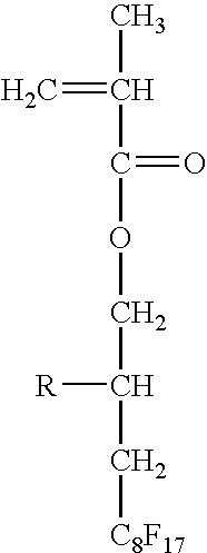
- A liquid poly(dimethylsiloxane) precursor is poured over a microfluidics master containing 100-μm features in the shape of channels. The wafer is then placed in an oven at 80° C. for 3 hours. The cured PDMS layer is then removed, trimmed, and inlet holes are punched through it using a luer stub. The layer is then treated with an oxygen plasma for 20 minutes followed by treatment with a silane coupling agent, aminopropyltriethoxy silane. Separately a second master containing 100-μm features in the shape of channels is spin coated with a small drop of a liquid PFPE dimethacrylate precursor plus functional monomer (where R is an epoxy) plus a photoinitiator over top of it at 3700 rpm for 1 minute to a thickness of about 20 μm. The wafer is then placed in a UV chamber and exposed to UV light (λ=365) for 10 minutes under a nitrogen purge. The thicker PDMS layer is then placed on top of the 20-μm thick layer and aligned in the desired area to form a seal. The layers are then placed in an oven and allowed to heat at 65° C. for 2 hours. The thin layer is then trimmed and the adhered layers are lifted from the master. Fluid inlet holes and outlet holes are punched using a luer stub. The bonded layers are then placed on a glass slide treated with a silane coupling agent, aminopropyltriethoxy silane, and allowed to heat at 65° C. for 15 hours permanently bonding the device to the glass slide. Small needles can then be placed in the inlets to introduce fluids and to actuate membrane valves as reported by Unger, M. et al. Science. 2000, 288, 113-6.

- A liquid PFPE dimethacrylate precursor is blended with a monomer having the structure shown below (where R is an amine group) and blended with 1 wt % of a free radical photoinitiator and poured over a microfluidics master containing 100-μm features in the shape of channels. A PDMS mold is used to contain the liquid in the desired area to a thickness of about 3 mm. The wafer is then placed in a UV chamber and exposed to UV light (λ=365) for 10 minutes under a nitrogen purge. The fully cured layer is then removed from the master and inlet holes are punched using a luer stub. Separately a second master containing 100-μm features in the shape of channels is spin coated with a small drop of the liquid PFPE precursor plus functional (where R is an epoxy group) over top of it at 3700 rpm for 1 minute to a thickness of about 20 μm. The wafer is then placed in a UV chamber and exposed to UV light (λ=365) for 10 minutes under a nitrogen purge. The thicker layer is then placed on top of the 20-μm thick layer and aligned in the desired area to form a seal. The layers are then placed in an oven and allowed to heat at 65° C. for 2 hours. The thin layer is then trimmed and the adhered layers are lifted from the master. Fluid inlet holes and outlet holes are punched using a luer stub. The bonded layers are then placed on a glass slide treated with a silane coupling agent, aminopropyltriethoxy silane, and allowed to heat at 65° C. for 15 hours permanently bonding the device to the glass slide. Small needles can then be placed in the inlets to introduce fluids and to actuate membrane valves as reported by Unger, M. et al. Science. 2000, 288, 113-6. An aqueous solution containing a protein functionalized with a free amine is then flowed through the channel which is lined with unreacted epoxy moieties, in such a way that the channel is then functionalized with the protein.

- A liquid PFPE dimethacrylate precursor is blended with a monomer having the structure shown below (where R is an amine group) and blended with 1 wt % of a free radical photoinitiator and poured over a microfluidics master containing 100-μm features in the shape of channels. A PDMS mold is used to contain the liquid in the desired area to a thickness of about 3 mm. The wafer is then placed in a UV chamber and exposed to UV light (A=365) for 10 minutes under a nitrogen purge. The fully cured layer is then removed from the master and inlet holes are punched using a luer stub. Separately a second master containing 100-μm features in the shape of channels is spin coated with a small drop of the liquid PFPE precursor plus functional (where R is an epoxy group) over top of it at 3700 rpm for 1 minute to a thickness of about 20 μm. The wafer is then placed in a UV chamber and exposed to UV light (λ=365) for 10 minutes under a nitrogen purge. The thicker layer is then placed on top of the 20-μm thick layer and aligned in the desired area to form a seal. The layers are then placed in an oven and allowed to heat at 65° C. for 2 hours. The thin layer is then trimmed and the adhered layers are lifted from the master. Fluid inlet holes and outlet holes are punched using a luer stub. The bonded layers are then placed on a glass slide treated with a silane coupling agent, aminopropyltriethoxy silane, and allowed to heat at 65° C. for 15 hours permanently bonding the device to the glass slide. Small needles can then be placed in the inlets to introduce fluids and to actuate membrane valves as reported by Unger, M. et al. Science. 2000, 288, 113-6. An aqueous solution containing a charged molecule functionalized with a free amine is then flowed through the channel which is lined with unreacted epoxy moieties, in such a way that the channel is then functionalized with the charged molecule.

- A smooth, flat PFPE layer is generated by drawing a doctor's blade across a small drop of the liquid PFPE dimethacrylate precursor across a glass slide. The Slide is then placed in a UV chamber and exposed to UV light (λ=365) for 10 minutes under a nitrogen purge. A scaffold composed of poly(lactic acid) in the shape of channels is laid on top of the flat, smooth layer of PFPE. A liquid PFPE dimethacrylate precursor is with 1 wt % of a free radical photoinitiator and poured over the scaffold. A PDMS mold is used to contain the liquid in the desired area to a thickness of about 3 mm. The apparatus is then placed in a UV chamber and exposed to UV light (λ=365) for 10 minutes under a nitrogen purge. The device is then heated at 150° C. for 24 hours to degrade the poly(lactic acid) thus revealing voids left in the shape of channels.
- A liquid PFPE dimethacrylate precursor is blended with 1 wt % of a free radical photoinitiator and poured over a microfluidics master containing 100-μm features in the shape of channels. A PDMS mold is used to contain the liquid in the desired area to a thickness of about 3 mm. The wafer is then placed in a UV chamber and exposed to UV light (λ=365) for 10 minutes under a nitrogen purge. Separately a second master containing 100-μm features in the shape of channels is spin coated with a small drop of the liquid PFPE precursor over top of it at 3700 rpm for 1 minute to a thickness of about 20 μm. The wafer is then placed in a UV chamber and exposed to UV light (λ=365) for 10 minutes under a nitrogen purge. The thicker layer is then removed, trimmed, and inlet holes are punched through it using a luer stub. The layer is then placed on top of the 20-μm thick layer and aligned in the desired area to form a seal. The layers are then placed in an oven and allowed to heat at 120° C. for 2 hours. The thin layer is then trimmed and the adhered layers are lifted from the master. Fluid inlet holes and outlet holes are punched using a luer stub. The bonded layers are then placed on a clean, glass slide in such a way that it forms as seal. The apparatus is exposed to 185 nm UV light for 20 minutes, forming a permanent bond between the device and the glass. Small needles can then be placed in the inlets to introduce fluids and to actuate membrane valves as reported by Unger, M. et al. Science. 2000, 288, 113-6.
- A liquid PFPE dimethacrylate precursor is blended with 1 wt % of a free radical photoinitiator and poured over a microfluidics master containing 100-μm features in the shape of channels. A PDMS mold is used to contain the liquid in the desired area to a thickness of about 3 mm. The wafer is then placed in a UV chamber and exposed to UV light (λ=365) for 10 minutes under a nitrogen purge. Separately a second master containing 100-μm features in the shape of channels is spin coated with a small drop of the liquid PFPE precursor over top of it at 3700 rpm for 1 minute to a thickness of about 20 μm. The wafer is then placed in a UV chamber and exposed to UV light (λ=365) for 10 minutes under a nitrogen purge. The thicker layer is then removed, trimmed, and inlet holes are punched through it using a luer stub. The layer is then placed on top of the 20-μm thick layer and aligned in the desired area to form a seal. The layers are then placed in an oven and allowed to heat at 120° C. for 2 hours. The thin layer is then trimmed and the adhered layers are lifted from the master. Fluid inlet holes and outlet holes are punched using a luer stub. The bonded layers are then placed on a clean, glass slide in such a way that it forms as seal. Small needles can then be placed in the inlets to introduce fluids and to actuate membrane valves as reported by Unger, M. et al. Science. 2000, 288, 113-6. The entire apparatus is then encased in a liquid epoxy precursor which is poured over the device allowed to cure. The casing serves to mechanically bind the device the substrate.
- A liquid PFPE precursor having the structure shown below (where the circle represents a linking molecule) is blended with 1 wt % of a free radical photoinitiator and poured over a microfluidics master containing 100-μm features in the shape of channels. A PDMS mold is used to contain the liquid in the desired area to a thickness of about 3 mm. The wafer is then placed in a UV chamber and exposed to UV light (λ=365) for 10 minutes under a nitrogen purge. Separately a second master containing 100-μm features in the shape of channels is spin coated with a small drop of the liquid PFPE precursor over top of it at 3700 rpm for 1 minute to a thickness of about 20 μm. The wafer is then placed in a UV chamber and exposed to UV light (λ=365) for 10 minutes under a nitrogen purge. Thirdly a smooth, flat PFPE layer is generated by drawing a doctor's blade across a small drop of the liquid PFPE precursor across a glass slide. The Slide is then placed in a UV chamber and exposed to UV light (λ=365) for 10 minutes under a nitrogen purge. The thicker layer is then removed, trimmed, and inlet holes are punched through it using a luer stub. The layer is then placed on top of the 20-μm thick layer and aligned in the desired area to form a seal. The layers are then placed in an oven and allowed to heat at 120° C. for 2 hours. The thin layer is then trimmed and the adhered layers are lifted from the master. Fluid inlet holes and outlet holes are punched using a luer stub. The bonded layers are then placed on the fully cured PFPE smooth layer on the glass slide and allowed to heat at 120° C. for 15 hours. Small needles can then be placed in the inlets to introduce fluids and to actuate membrane valves as reported by Unger, M. et al. Science. 2000, 288, 113-6.

- A master containing 100-μm features in the shape of channels is spin coated with a small drop of the liquid PFPE dimethacrylate precursor containing photoinitiator over top of it at 3700 rpm for 1 minute to a thickness of about 20 μm. A PDMS dimethacrylate containing photoinitiator is then poured over top of the thin PFPE layer to a thickness of 3 mm. The wafer is then placed in a UV chamber and exposed to UV light (λ=365) for 10 minutes under a nitrogen purge. The layer is then removed, trimmed, and inlet holes are punched through it using a luer stub. The hybrid device is then placed on a glass slide and a seal is formed. Small needles can then be placed in the inlets to introduce fluids.
- It will be understood that various details of the presently disclosed subject matter can be changed without departing from the scope of the presently disclosed subject matter. Furthermore, the foregoing description is for the purpose of illustration only, and not for the purpose of limitation.
Claims (238)


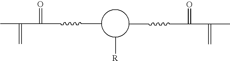


Priority Applications (1)
| Application Number | Priority Date | Filing Date | Title |
|---|---|---|---|
| US10/589,222 US20070275193A1 (en) | 2004-02-13 | 2005-02-14 | Functional Materials and Novel Methods for the Fabrication of Microfluidic Devices |
Applications Claiming Priority (3)
| Application Number | Priority Date | Filing Date | Title |
|---|---|---|---|
| US54490504P | 2004-02-13 | 2004-02-13 | |
| PCT/US2005/004421 WO2005084191A2 (en) | 2004-02-13 | 2005-02-14 | Functional materials and novel methods for the fabrication of microfluidic devices |
| US10/589,222 US20070275193A1 (en) | 2004-02-13 | 2005-02-14 | Functional Materials and Novel Methods for the Fabrication of Microfluidic Devices |
Publications (1)
| Publication Number | Publication Date |
|---|---|
| US20070275193A1 true US20070275193A1 (en) | 2007-11-29 |
Family
ID=34919322
Family Applications (1)
| Application Number | Title | Priority Date | Filing Date |
|---|---|---|---|
| US10/589,222 Abandoned US20070275193A1 (en) | 2004-02-13 | 2005-02-14 | Functional Materials and Novel Methods for the Fabrication of Microfluidic Devices |
Country Status (8)
| Country | Link |
|---|---|
| US (1) | US20070275193A1 (en) |
| EP (1) | EP1737574A4 (en) |
| JP (1) | JP2007527784A (en) |
| CN (1) | CN101189271A (en) |
| AU (1) | AU2005220150A1 (en) |
| CA (1) | CA2555912A1 (en) |
| SG (1) | SG150506A1 (en) |
| WO (1) | WO2005084191A2 (en) |
Cited By (80)
| Publication number | Priority date | Publication date | Assignee | Title |
|---|---|---|---|---|
| US20060286775A1 (en) * | 2005-06-21 | 2006-12-21 | Singh Kaushal K | Method for forming silicon-containing materials during a photoexcitation deposition process |
| WO2007002040A2 (en) * | 2005-06-21 | 2007-01-04 | Applied Materials, Inc. | Method for forming silicon-containing materials during a photoexcitation deposition process |
| US20070254278A1 (en) * | 2003-09-23 | 2007-11-01 | Desimone Joseph M | Photocurable Perfluoropolyethers for Use as Novel Materials in Microfluidic Devices |
| US20080202928A1 (en) * | 2007-01-23 | 2008-08-28 | Hyun Seok Jung | Multi-layer strip for use in measuring biological material and system for measuring biological material |
| WO2009100462A2 (en) * | 2008-02-10 | 2009-08-13 | Microdysis, Inc. | Polymer surface functionalization and related applications |
| US20090216104A1 (en) * | 2005-08-26 | 2009-08-27 | Desimone Joseph M | Use of acid derivatives of fluoropolymers for fouling-resistant surfaces |
| WO2009140671A2 (en) | 2008-05-16 | 2009-11-19 | Advanced Liquid Logic, Inc. | Droplet actuator devices and methods for manipulating beads |
| US7651955B2 (en) | 2005-06-21 | 2010-01-26 | Applied Materials, Inc. | Method for forming silicon-containing materials during a photoexcitation deposition process |
| US20100038649A1 (en) * | 2008-08-14 | 2010-02-18 | Samsung Electronics Co., Ltd. | Mold, manufacturing method of mold, method for forming patterns using mold, and display substrate and display device manufactured by using method for forming patterns |
| US20100173113A1 (en) * | 2008-12-05 | 2010-07-08 | Liquidia Technologies, Inc. | Method for producing patterned materials |
| US7761130B2 (en) | 2003-07-25 | 2010-07-20 | Dexcom, Inc. | Dual electrode system for a continuous analyte sensor |
| US20100200781A1 (en) * | 2009-02-06 | 2010-08-12 | Maziyar Khorasani | Method and apparatus for manipulating and detecting analytes |
| WO2010097740A1 (en) * | 2009-02-24 | 2010-09-02 | Services Petroliers Schlumberger | Micro-valve and micro-fluidic device using such |
| US7792562B2 (en) | 1997-03-04 | 2010-09-07 | Dexcom, Inc. | Device and method for determining analyte levels |
| US7828728B2 (en) | 2003-07-25 | 2010-11-09 | Dexcom, Inc. | Analyte sensor |
| US7871570B2 (en) | 2007-02-23 | 2011-01-18 | Joseph Zhili Huang | Fluidic array devices and systems, and related methods of use and manufacturing |
| WO2011008940A1 (en) * | 2009-07-15 | 2011-01-20 | The Penn State Research Foundation | Polymer blends of electrostrictive terpolymer with other polymers |
| US7885697B2 (en) | 2004-07-13 | 2011-02-08 | Dexcom, Inc. | Transcutaneous analyte sensor |
| US20110085949A1 (en) * | 2009-10-08 | 2011-04-14 | Emmanuel Roy | Microfluidic device, composition and method of forming |
| US20110102940A1 (en) * | 2009-11-02 | 2011-05-05 | Hitachi Global Storage Technologies Netherlands B.V. | System, method and apparatus for planarizing surfaces with functionalized polymers |
| US7976759B2 (en) | 2007-10-12 | 2011-07-12 | Liquidia Technologies, Inc. | System and method for producing particles and patterned films |
| WO2011103041A1 (en) * | 2010-02-18 | 2011-08-25 | Yu Chris C | Method of fabricating micro-devices |
| CN102225506A (en) * | 2011-05-04 | 2011-10-26 | 中国地质大学(武汉) | Method for fabricating onboard micro channel structure for microfluidic control |
| US8050731B2 (en) | 2002-05-22 | 2011-11-01 | Dexcom, Inc. | Techniques to improve polyurethane membranes for implantable glucose sensors |
| US8064977B2 (en) | 2002-05-22 | 2011-11-22 | Dexcom, Inc. | Silicone based membranes for use in implantable glucose sensors |
| US20120022705A1 (en) * | 2007-12-04 | 2012-01-26 | Ludwig Lester F | Multi-channel chemical transport bus with bus-associated sensors for microfluidic and other applications |
| WO2012018709A2 (en) * | 2010-08-06 | 2012-02-09 | Arkema Inc. | Superacid functional compounds |
| USRE43399E1 (en) | 2003-07-25 | 2012-05-22 | Dexcom, Inc. | Electrode systems for electrochemical sensors |
| US8255033B2 (en) | 2003-07-25 | 2012-08-28 | Dexcom, Inc. | Oxygen enhancing membrane systems for implantable devices |
| US8277713B2 (en) | 2004-05-03 | 2012-10-02 | Dexcom, Inc. | Implantable analyte sensor |
| US8290559B2 (en) | 2007-12-17 | 2012-10-16 | Dexcom, Inc. | Systems and methods for processing sensor data |
| US20130019696A1 (en) * | 2009-05-29 | 2013-01-24 | Waters Technologies Corporation | Chromatography Apparatus And Methods Using Multiple Microfluidic Substrates |
| US8364229B2 (en) | 2003-07-25 | 2013-01-29 | Dexcom, Inc. | Analyte sensors having a signal-to-noise ratio substantially unaffected by non-constant noise |
| US8417312B2 (en) | 2007-10-25 | 2013-04-09 | Dexcom, Inc. | Systems and methods for processing sensor data |
| US8509871B2 (en) | 2001-07-27 | 2013-08-13 | Dexcom, Inc. | Sensor head for use with implantable devices |
| US8560039B2 (en) | 2008-09-19 | 2013-10-15 | Dexcom, Inc. | Particle-containing membrane and particulate electrode for analyte sensors |
| US8562558B2 (en) | 2007-06-08 | 2013-10-22 | Dexcom, Inc. | Integrated medicament delivery device for use with continuous analyte sensor |
| US8583204B2 (en) | 2008-03-28 | 2013-11-12 | Dexcom, Inc. | Polymer membranes for continuous analyte sensors |
| US8682408B2 (en) | 2008-03-28 | 2014-03-25 | Dexcom, Inc. | Polymer membranes for continuous analyte sensors |
| US8744546B2 (en) | 2005-05-05 | 2014-06-03 | Dexcom, Inc. | Cellulosic-based resistance domain for an analyte sensor |
| US8929968B2 (en) | 2003-12-05 | 2015-01-06 | Dexcom, Inc. | Dual electrode system for a continuous analyte sensor |
| US9135402B2 (en) | 2007-12-17 | 2015-09-15 | Dexcom, Inc. | Systems and methods for processing sensor data |
| US9439589B2 (en) | 1997-03-04 | 2016-09-13 | Dexcom, Inc. | Device and method for determining analyte levels |
| US20170127991A1 (en) * | 2011-04-29 | 2017-05-11 | Seventh Sense Biosystems, Inc. | Systems and methods for collection and/or manipulation of blood spots or other bodily fluids |
| US9763609B2 (en) | 2003-07-25 | 2017-09-19 | Dexcom, Inc. | Analyte sensors having a signal-to-noise ratio substantially unaffected by non-constant noise |
| US9986942B2 (en) | 2004-07-13 | 2018-06-05 | Dexcom, Inc. | Analyte sensor |
| US10052627B2 (en) | 2013-10-18 | 2018-08-21 | Endress + Hauser Flowtec Ag | Measuring arrangement having a support element and a sensor |
| US20180370125A1 (en) * | 2015-12-22 | 2018-12-27 | Carbon, Inc. | Fabrication of compound products from multiple intermediates by additive manufacturing with dual cure resins |
| US10189983B2 (en) | 2012-12-28 | 2019-01-29 | Toyo Gosei Co., Ltd. | Curable resin composition, resin mold for imprinting, method for photo imprinting, method for manufacturing semiconductor integrated circuit, and method for manufacturing fine optical element |
| US10272426B2 (en) * | 2015-04-21 | 2019-04-30 | Jsr Corporation | Method of producing microfluidic device, microfluidic device, and photosensitive resin composition |
| US10361313B2 (en) * | 2016-07-13 | 2019-07-23 | Electronics And Telecommunications Research Institute | Electronic device and methods of fabricating the same |
| US10472446B2 (en) | 2013-03-04 | 2019-11-12 | Toyo Gosei Co., Ltd. | Composition, resin mold, photo imprinting method, method for manufacturing optical element, and method for manufacturing electronic element |
| US10543310B2 (en) | 2011-12-19 | 2020-01-28 | Seventh Sense Biosystems, Inc. | Delivering and/or receiving material with respect to a subject surface |
| US10544260B2 (en) | 2017-08-30 | 2020-01-28 | Ppg Industries Ohio, Inc. | Fluoropolymers, methods of preparing fluoropolymers, and coating compositions containing fluoropolymers |
| US10610136B2 (en) | 2005-03-10 | 2020-04-07 | Dexcom, Inc. | System and methods for processing analyte sensor data for sensor calibration |
| EP3558527A4 (en) * | 2016-12-20 | 2020-06-24 | Bio-Rad Laboratories, Inc. | Uv graft on microfluidic devices |
| US10791928B2 (en) | 2007-05-18 | 2020-10-06 | Dexcom, Inc. | Analyte sensors having a signal-to-noise ratio substantially unaffected by non-constant noise |
| US10799166B2 (en) | 2009-03-02 | 2020-10-13 | Seventh Sense Biosystems, Inc. | Delivering and/or receiving fluids |
| US10813577B2 (en) | 2005-06-21 | 2020-10-27 | Dexcom, Inc. | Analyte sensor |
| US10828883B2 (en) * | 2012-09-12 | 2020-11-10 | International Business Machines Corporation | Thermally cross-linkable photo-hydrolyzable inkjet printable polymers for microfluidic channels |
| US10835163B2 (en) | 2011-04-29 | 2020-11-17 | Seventh Sense Biosystems, Inc. | Systems and methods for collecting fluid from a subject |
| US10835672B2 (en) | 2004-02-26 | 2020-11-17 | Dexcom, Inc. | Integrated insulin delivery system with continuous glucose sensor |
| US10939860B2 (en) | 2009-03-02 | 2021-03-09 | Seventh Sense Biosystems, Inc. | Techniques and devices associated with blood sampling |
| US10966609B2 (en) | 2004-02-26 | 2021-04-06 | Dexcom, Inc. | Integrated medicament delivery device for use with continuous analyte sensor |
| US11118223B2 (en) * | 2019-03-14 | 2021-09-14 | Ultima Genomics, Inc. | Methods, devices, and systems for analyte detection and analysis |
| US20210300100A1 (en) * | 2020-03-31 | 2021-09-30 | Canon Production Printing Holding B.V. | Method for applying an image onto the recording medium and corresponding printing apparatus |
| WO2021198827A1 (en) * | 2020-03-31 | 2021-10-07 | 3M Innovative Properties Company | Diagnostic device |
| US11155868B2 (en) | 2019-03-14 | 2021-10-26 | Ultima Genomics, Inc. | Methods, devices, and systems for analyte detection and analysis |
| US11177029B2 (en) | 2010-08-13 | 2021-11-16 | Yourbio Health, Inc. | Systems and techniques for monitoring subjects |
| US11202895B2 (en) | 2010-07-26 | 2021-12-21 | Yourbio Health, Inc. | Rapid delivery and/or receiving of fluids |
| US11246990B2 (en) | 2004-02-26 | 2022-02-15 | Dexcom, Inc. | Integrated delivery device for continuous glucose sensor |
| US11331022B2 (en) | 2017-10-24 | 2022-05-17 | Dexcom, Inc. | Pre-connected analyte sensors |
| US11350862B2 (en) | 2017-10-24 | 2022-06-07 | Dexcom, Inc. | Pre-connected analyte sensors |
| US11396015B2 (en) | 2018-12-07 | 2022-07-26 | Ultima Genomics, Inc. | Implementing barriers for controlled environments during sample processing and detection |
| US11399745B2 (en) | 2006-10-04 | 2022-08-02 | Dexcom, Inc. | Dual electrode system for a continuous analyte sensor |
| US11499962B2 (en) | 2017-11-17 | 2022-11-15 | Ultima Genomics, Inc. | Methods and systems for analyte detection and analysis |
| US11512350B2 (en) | 2017-11-17 | 2022-11-29 | Ultima Genomics, Inc. | Methods for biological sample processing and analysis |
| US11633133B2 (en) | 2003-12-05 | 2023-04-25 | Dexcom, Inc. | Dual electrode system for a continuous analyte sensor |
| US11730407B2 (en) | 2008-03-28 | 2023-08-22 | Dexcom, Inc. | Polymer membranes for continuous analyte sensors |
| WO2023224993A1 (en) * | 2022-05-16 | 2023-11-23 | Xbiologix, Inc. | Rapid detection tests and methods of forming the same |
Families Citing this family (50)
| Publication number | Priority date | Publication date | Assignee | Title |
|---|---|---|---|---|
| WO2006060748A2 (en) | 2004-12-03 | 2006-06-08 | California Institute Of Technology | Microfluidic sieve valves |
| US7686907B1 (en) | 2005-02-01 | 2010-03-30 | Brigham Young University | Phase-changing sacrificial materials for manufacture of high-performance polymeric capillary microchips |
| EP2703499A1 (en) | 2005-06-02 | 2014-03-05 | Fluidigm Corporation | Analysis using microfluidic partitioning devices to generate single cell samples |
| EP2537657A3 (en) * | 2005-08-09 | 2016-05-04 | The University of North Carolina At Chapel Hill | Methods and materials for fabricating microfluidic devices |
| US8945361B2 (en) | 2005-09-20 | 2015-02-03 | ProteinSimple | Electrophoresis standards, methods and kits |
| US20080286152A1 (en) | 2005-11-08 | 2008-11-20 | Ecole Polytechinque Federale De Lausanne | Hyperbrached Polymer for Micro Devices |
| JP2007189961A (en) * | 2006-01-20 | 2007-08-02 | Toppan Printing Co Ltd | Method for producing container and surface-treating apparatus |
| DE602006009381D1 (en) * | 2006-06-08 | 2009-11-05 | Dwi An Der Rwth Aachen E V | Structuring of hydrogels |
| DE102006029051A1 (en) * | 2006-06-24 | 2007-12-27 | Forschungszentrum Jülich GmbH | Cell culture device, method of making the device and cell culture method |
| US20080017512A1 (en) * | 2006-07-24 | 2008-01-24 | Bordunov Andrei V | Coatings for capillaries capable of capturing analytes |
| WO2008067386A2 (en) * | 2006-11-28 | 2008-06-05 | Drexel University | Piezoelectric microcantilever sensors for biosensing |
| US8642288B2 (en) * | 2007-06-07 | 2014-02-04 | Technion Research & Development Foundation Ltd. | Methods for viscoelastic focusing of particles |
| US7737307B2 (en) | 2007-08-06 | 2010-06-15 | E. I. Du Pont De Nemours And Company | Fluorinated nonionic surfactants |
| US8741663B2 (en) | 2008-03-11 | 2014-06-03 | Drexel University | Enhanced detection sensitivity with piezoelectric sensors |
| US8383202B2 (en) | 2008-06-13 | 2013-02-26 | Kateeva, Inc. | Method and apparatus for load-locked printing |
| US8899171B2 (en) | 2008-06-13 | 2014-12-02 | Kateeva, Inc. | Gas enclosure assembly and system |
| US9048344B2 (en) | 2008-06-13 | 2015-06-02 | Kateeva, Inc. | Gas enclosure assembly and system |
| US10434804B2 (en) | 2008-06-13 | 2019-10-08 | Kateeva, Inc. | Low particle gas enclosure systems and methods |
| CN101903174B (en) | 2008-08-11 | 2014-04-02 | 北京大学 | Superhydrophobic poly(dimethylsiloxane) and methods for making the same |
| US8097639B2 (en) | 2008-08-29 | 2012-01-17 | Peking University | Light sensitive PDMS for complex pattern formation |
| CN101835739B (en) | 2008-08-29 | 2013-10-09 | 北京大学 | A light sensitive initiator integrated poly(dimethylsiloxane) |
| EP2221664A1 (en) * | 2009-02-19 | 2010-08-25 | Solvay Solexis S.p.A. | Nanolithography process |
| WO2010102194A1 (en) | 2009-03-06 | 2010-09-10 | Waters Technologies Corporation | Electrospray interface to a microfluidic substrate |
| JP5985390B2 (en) | 2009-04-02 | 2016-09-06 | フリューダイム・コーポレイション | Multi-primer amplification method for adding barcode to target nucleic acid |
| ITMI20110995A1 (en) | 2011-05-31 | 2012-12-01 | Ione | METHOD FOR THE PRODUCTION OF MONOLITHIC THREE-DIMENSIONAL MICROFLUID DEVICES |
| EP3627140A1 (en) | 2012-02-29 | 2020-03-25 | Fluidigm Corporation | Methods, systems, and devices for multiple single-cell capturing and processing using microfluidics |
| CN104471077B (en) | 2012-05-21 | 2017-05-24 | 富鲁达公司 | Single-particle analysis of particle populations |
| JP6261005B2 (en) * | 2012-11-30 | 2018-01-17 | 国立大学法人京都大学 | Macroporous monolith and method for producing the same |
| JP6284142B2 (en) * | 2013-01-13 | 2018-02-28 | 国立大学法人京都大学 | Macroporous monolith, its production method and its application |
| EP3581641A1 (en) | 2013-03-15 | 2019-12-18 | Fluidigm Corporation | Methods and devices for analysis of defined multicellular combinations |
| WO2014171431A1 (en) * | 2013-04-19 | 2014-10-23 | Jsr株式会社 | Curable resin composition for forming microchannel, and microchannel |
| JP2014210865A (en) * | 2013-04-19 | 2014-11-13 | Jsr株式会社 | Radiation curable resin composition for forming microflow channel, and microflow channel |
| DE102013007298A1 (en) * | 2013-04-26 | 2014-10-30 | Basf Se | Process and supply unit for restabilization of radically polymerizable monomers |
| GB2516670A (en) * | 2013-07-29 | 2015-02-04 | Atlas Genetics Ltd | Fluid control device and method of manufacture |
| EP3052219B1 (en) | 2013-10-01 | 2020-04-22 | The Broad Institute, Inc. | Sieve valves, microfluidic circuits, microfluidic devices, kits, and methods for isolating an analyte |
| KR101878084B1 (en) | 2013-12-26 | 2018-07-12 | 카티바, 인크. | Apparatus and techniques for thermal treatment of electronic devices |
| KR20220147699A (en) | 2014-01-21 | 2022-11-03 | 카티바, 인크. | Apparatus and techniques for electronic device encapsulation |
| JP6461195B2 (en) | 2014-04-30 | 2019-01-30 | カティーバ, インコーポレイテッド | Gas cushion apparatus and technique for substrate coating |
| WO2017124101A2 (en) | 2016-01-15 | 2017-07-20 | The Broad Institute Inc. | Semi-permeable arrays for analyzing biological systems and methods of using same |
| WO2018027009A1 (en) * | 2016-08-05 | 2018-02-08 | Microoptx Inc. | Polymeric devices and methods of making |
| WO2019054500A1 (en) * | 2017-09-15 | 2019-03-21 | Agc株式会社 | Microchannel chip |
| BR112020012089A2 (en) * | 2017-12-26 | 2020-11-17 | Akzo Nobel Coatings International B.V. | fluoride ether polymer, method of its preparation and its use and coating composition |
| US11084032B2 (en) | 2018-08-28 | 2021-08-10 | International Business Machines Corporation | Method to create multilayer microfluidic chips using spin-on carbon as gap fill and spin-on glass tone inversion |
| US11192101B2 (en) | 2018-08-28 | 2021-12-07 | International Business Machines Corporation | Method to create multilayer microfluidic chips using spin-on carbon as gap filling materials |
| US11305277B2 (en) | 2018-12-10 | 2022-04-19 | Shenzhen University | Micro-structured mold-core of microfluidic chip and its manufacturing method |
| GB201913529D0 (en) * | 2019-09-19 | 2019-11-06 | Tanriverdi Ugur | Method And Apparatus |
| CN113083383B (en) * | 2021-03-18 | 2022-10-25 | 华中农业大学 | Microfluidic chip device, preparation method and soil microbial community culture method |
| KR102630830B1 (en) * | 2021-08-11 | 2024-01-29 | 주식회사 에이아이더뉴트리진 | Method for Fabrication of Microfluidic Device Using Transfer Film |
| CN114682312B (en) * | 2022-03-30 | 2023-06-13 | 北京航空航天大学 | Silicon-based droplet self-transporting microstructure and transporting method |
| CN114989344B (en) * | 2022-06-14 | 2023-09-19 | 万华化学集团股份有限公司 | Vinylidene fluoride copolymer, preparation method thereof and application thereof in lithium ion battery |
Citations (88)
| Publication number | Priority date | Publication date | Assignee | Title |
|---|---|---|---|---|
| US3810874A (en) * | 1969-03-10 | 1974-05-14 | Minnesota Mining & Mfg | Polymers prepared from poly(perfluoro-alkylene oxide) compounds |
| US4512848A (en) * | 1984-02-06 | 1985-04-23 | Exxon Research And Engineering Co. | Procedure for fabrication of microstructures over large areas using physical replication |
| US4614667A (en) * | 1984-05-21 | 1986-09-30 | Minnesota Mining And Manufacturing Company | Composite low surface energy liner of perfluoropolyether |
| US4663274A (en) * | 1985-04-01 | 1987-05-05 | Polaroid Corporation | Method for forming a photosensitive silver halide element |
| US4681925A (en) * | 1985-02-22 | 1987-07-21 | Ausimont S.P.A. | Fluorinated polyacrylates and polyacrylamides having a controlled cross-linking degree, and process for preparing same |
| US4818801A (en) * | 1982-01-18 | 1989-04-04 | Minnesota Mining And Manufacturing Company | Ophthalmic device comprising a polymer of a telechelic perfluoropolyether |
| US4830910A (en) * | 1987-11-18 | 1989-05-16 | Minnesota Mining And Manufacturing Company | Low adhesion compositions of perfluoropolyethers |
| US5041359A (en) * | 1985-04-03 | 1991-08-20 | Stork Screens B.V. | Method for forming a patterned photopolymer coating on a printing roller |
| US5189135A (en) * | 1989-06-28 | 1993-02-23 | Syremont S.P.A. | Fluorinated polyurethanes with hydroxy functionality, process for preparing them and their use for the treatment of lithoidal material |
| US5279689A (en) * | 1989-06-30 | 1994-01-18 | E. I. Du Pont De Nemours And Company | Method for replicating holographic optical elements |
| US5412034A (en) * | 1993-10-26 | 1995-05-02 | E. I. Du Pont De Nemours And Company | Curable elastomeric blends |
| US5425848A (en) * | 1993-03-16 | 1995-06-20 | U.S. Philips Corporation | Method of providing a patterned relief of cured photoresist on a flat substrate surface and device for carrying out such a method |
| US5512131A (en) * | 1993-10-04 | 1996-04-30 | President And Fellows Of Harvard College | Formation of microstamped patterns on surfaces and derivative articles |
| US5593130A (en) * | 1993-06-09 | 1997-01-14 | Pharmacia Biosensor Ab | Valve, especially for fluid handling bodies with microflowchannels |
| US5630902A (en) * | 1994-12-30 | 1997-05-20 | Honeywell Inc. | Apparatus for use in high fidelty replication of diffractive optical elements |
| US5751150A (en) * | 1995-08-11 | 1998-05-12 | Aerovironment | Bidirectional load and source cycler |
| US5772905A (en) * | 1995-11-15 | 1998-06-30 | Regents Of The University Of Minnesota | Nanoimprint lithography |
| US6015609A (en) * | 1996-04-04 | 2000-01-18 | Navartis Ag | Process for manufacture of a porous polymer from a mixture |
| US6024296A (en) * | 1998-08-10 | 2000-02-15 | Caterpillar, Inc. | Direct control fuel injector with dual flow rate orifice |
| US6027630A (en) * | 1997-04-04 | 2000-02-22 | University Of Southern California | Method for electrochemical fabrication |
| US6027595A (en) * | 1998-07-02 | 2000-02-22 | Samsung Electronics Co., Ltd. | Method of making optical replicas by stamping in photoresist and replicas formed thereby |
| US6083971A (en) * | 1996-07-18 | 2000-07-04 | Hoffmann-La Roche Inc. | Certain oxopyrolo-pyrrole derivatives having thrombin inhibiting activity |
| US6183829B1 (en) * | 1997-11-07 | 2001-02-06 | Rohm And Haas Company | Process and apparatus for forming plastic sheet |
| US6204296B1 (en) * | 1992-10-27 | 2001-03-20 | Alliance Pharmaceutical Corp. | Patient oxygenation using stabilized fluorocarbon emulsions |
| US6207758B1 (en) * | 1997-12-15 | 2001-03-27 | Ausimont S.P.A. | Fluorinated thermoplastic elastomers |
| US6228318B1 (en) * | 1999-03-24 | 2001-05-08 | Sumitomo Electric Industries, Ltd. | Manufacturing method of ceramics component having microstructure |
| US6247986B1 (en) * | 1998-12-23 | 2001-06-19 | 3M Innovative Properties Company | Method for precise molding and alignment of structures on a substrate using a stretchable mold |
| US6280808B1 (en) * | 1999-05-25 | 2001-08-28 | Rohm And Haas Company | Process and apparatus for forming plastic sheet |
| US6284072B1 (en) * | 1996-11-09 | 2001-09-04 | Epigem Limited | Multifunctional microstructures and preparation thereof |
| US6294450B1 (en) * | 2000-03-01 | 2001-09-25 | Hewlett-Packard Company | Nanoscale patterning for the formation of extensive wires |
| US6335224B1 (en) * | 2000-05-16 | 2002-01-01 | Sandia Corporation | Protection of microelectronic devices during packaging |
| US6334960B1 (en) * | 1999-03-11 | 2002-01-01 | Board Of Regents, The University Of Texas System | Step and flash imprint lithography |
| US6355198B1 (en) * | 1996-03-15 | 2002-03-12 | President And Fellows Of Harvard College | Method of forming articles including waveguides via capillary micromolding and microtransfer molding |
| US6375870B1 (en) * | 1998-11-17 | 2002-04-23 | Corning Incorporated | Replicating a nanoscale pattern |
| US6408878B2 (en) * | 1999-06-28 | 2002-06-25 | California Institute Of Technology | Microfabricated elastomeric valve and pump systems |
| US6422528B1 (en) * | 2001-01-17 | 2002-07-23 | Sandia National Laboratories | Sacrificial plastic mold with electroplatable base |
| US20030006527A1 (en) * | 2001-06-22 | 2003-01-09 | Rabolt John F. | Method of fabricating micron-and submicron-scale elastomeric templates for surface patterning |
| US6508988B1 (en) * | 2000-10-03 | 2003-01-21 | California Institute Of Technology | Combinatorial synthesis system |
| US6518189B1 (en) * | 1995-11-15 | 2003-02-11 | Regents Of The University Of Minnesota | Method and apparatus for high density nanostructures |
| US6517995B1 (en) * | 1999-09-14 | 2003-02-11 | Massachusetts Institute Of Technology | Fabrication of finely featured devices by liquid embossing |
| US20030062334A1 (en) * | 2001-09-25 | 2003-04-03 | Lee Hong Hie | Method for forming a micro-pattern on a substrate by using capillary force |
| US20030071016A1 (en) * | 2001-10-11 | 2003-04-17 | Wu-Sheng Shih | Patterned structure reproduction using nonsticking mold |
| US6555221B1 (en) * | 1998-10-26 | 2003-04-29 | The University Of Tokyo | Method for forming an ultra microparticle-structure |
| US20030139521A1 (en) * | 2001-05-21 | 2003-07-24 | Linert Jeffrey G. | Polymers containing perfluorovinyl ethers and applications for such polymers |
| US6607683B1 (en) * | 1998-09-04 | 2003-08-19 | Bruce E. Harrington | Methods and apparatus for producing manufactured articles having natural characteristics |
| US6686184B1 (en) * | 2000-05-25 | 2004-02-03 | President And Fellows Of Harvard College | Patterning of surfaces utilizing microfluidic stamps including three-dimensionally arrayed channel networks |
| US6689900B2 (en) * | 2001-02-09 | 2004-02-10 | E. I. Du Pont De Nemours And Company | Fluorinated crosslinker and composition |
| US20040028804A1 (en) * | 2002-08-07 | 2004-02-12 | Anderson Daniel G. | Production of polymeric microarrays |
| US6696220B2 (en) * | 2000-10-12 | 2004-02-24 | Board Of Regents, The University Of Texas System | Template for room temperature, low pressure micro-and nano-imprint lithography |
| US6699347B2 (en) * | 2002-05-20 | 2004-03-02 | The Procter & Gamble Company | High speed embossing and adhesive printing process |
| US20040046271A1 (en) * | 2002-09-05 | 2004-03-11 | Watts Michael P.C. | Functional patterning material for imprint lithography processes |
| US6705357B2 (en) * | 2000-09-18 | 2004-03-16 | President And Fellows Of Harvard College | Method and apparatus for gradient generation |
| US20040053009A1 (en) * | 2000-06-07 | 2004-03-18 | Ozin Geoffrey Alan | Method of self-assembly and optical applications of crystalline colloidal patterns on substrates |
| US20040065252A1 (en) * | 2002-10-04 | 2004-04-08 | Sreenivasan Sidlgata V. | Method of forming a layer on a substrate to facilitate fabrication of metrology standards |
| US6719868B1 (en) * | 1998-03-23 | 2004-04-13 | President And Fellows Of Harvard College | Methods for fabricating microfluidic structures |
| US20040084402A1 (en) * | 2000-10-05 | 2004-05-06 | Ashmead James William | Polymeric microfabricated fluidic device suitable for ultraviolet detection |
| US20040110856A1 (en) * | 2002-12-04 | 2004-06-10 | Young Jung Gun | Polymer solution for nanoimprint lithography to reduce imprint temperature and pressure |
| US6753131B1 (en) * | 1996-07-22 | 2004-06-22 | President And Fellows Of Harvard College | Transparent elastomeric, contact-mode photolithography mask, sensor, and wavefront engineering element |
| US6755984B2 (en) * | 2002-10-24 | 2004-06-29 | Hewlett-Packard Development Company, L.P. | Micro-casted silicon carbide nano-imprinting stamp |
| US6759182B2 (en) * | 2001-03-06 | 2004-07-06 | Omron Corporation | Manufacturing method and apparatus of optical device and reflection plate provided with resin thin film having micro-asperity pattern |
| US20040137734A1 (en) * | 1995-11-15 | 2004-07-15 | Princeton University | Compositions and processes for nanoimprinting |
| US6766817B2 (en) * | 2001-07-25 | 2004-07-27 | Tubarc Technologies, Llc | Fluid conduction utilizing a reversible unsaturated siphon with tubarc porosity action |
| US6767706B2 (en) * | 2000-06-05 | 2004-07-27 | California Institute Of Technology | Integrated active flux microfluidic devices and methods |
| US6770721B1 (en) * | 2000-11-02 | 2004-08-03 | Surface Logix, Inc. | Polymer gel contact masks and methods and molds for making same |
| US6783717B2 (en) * | 2002-04-22 | 2004-08-31 | International Business Machines Corporation | Process of fabricating a precision microcontact printing stamp |
| US6841079B2 (en) * | 2002-05-31 | 2005-01-11 | 3M Innovative Properties Company | Fluorochemical treatment for silicon articles |
| US6849558B2 (en) * | 2002-05-22 | 2005-02-01 | The Board Of Trustees Of The Leland Stanford Junior University | Replication and transfer of microstructures and nanostructures |
| US20050038180A1 (en) * | 2003-08-13 | 2005-02-17 | Jeans Albert H. | Silicone elastomer material for high-resolution lithography |
| US6860956B2 (en) * | 2003-05-23 | 2005-03-01 | Agency For Science, Technology & Research | Methods of creating patterns on substrates and articles of manufacture resulting therefrom |
| US20050048581A1 (en) * | 2003-08-25 | 2005-03-03 | Chiu Daniel T. | Method and device for biochemical detection and analysis of subcellular compartments from a single cell |
| US6869557B1 (en) * | 2002-03-29 | 2005-03-22 | Seagate Technology Llc | Multi-level stamper for improved thermal imprint lithography |
| US20050061773A1 (en) * | 2003-08-21 | 2005-03-24 | Byung-Jin Choi | Capillary imprinting technique |
| US6900881B2 (en) * | 2002-07-11 | 2005-05-31 | Molecular Imprints, Inc. | Step and repeat imprint lithography systems |
| US20050120902A1 (en) * | 2001-04-25 | 2005-06-09 | David Adams | Edge transfer lithography |
| US6923930B2 (en) * | 2000-01-21 | 2005-08-02 | Obducat Aktiebolag | Mold for nano imprinting |
| US6929899B2 (en) * | 2001-01-25 | 2005-08-16 | E. I. Du Pont De Nemours And Company | Fluorinated photopolymer composition and waveguide device |
| US6929030B2 (en) * | 1999-06-28 | 2005-08-16 | California Institute Of Technology | Microfabricated elastomeric valve and pump systems |
| US6932934B2 (en) * | 2002-07-11 | 2005-08-23 | Molecular Imprints, Inc. | Formation of discontinuous films during an imprint lithography process |
| US6936181B2 (en) * | 2001-10-11 | 2005-08-30 | Kovio, Inc. | Methods for patterning using liquid embossing |
| US20060009805A1 (en) * | 2004-04-26 | 2006-01-12 | Ralph Jensen | Neural stimulation device employing renewable chemical stimulation |
| US20060021533A1 (en) * | 2004-07-30 | 2006-02-02 | Jeans Albert H | Imprint stamp |
| US20060022131A1 (en) * | 2003-03-04 | 2006-02-02 | Hiromasa Tojo | Electrospray emitter coated with material of low surface energy |
| US20060077221A1 (en) * | 2003-11-04 | 2006-04-13 | Lexmark International, Inc. | Microfluidic substrates having improved fluidic channels |
| US20060083971A1 (en) * | 2004-01-23 | 2006-04-20 | The University Of North Carolina At Chapel Hill North Carolina State University | Liquid materials for use in electrochemical cells |
| US7070406B2 (en) * | 2003-04-29 | 2006-07-04 | Hewlett-Packard Development Company, L.P. | Apparatus for embossing a flexible substrate with a pattern carried by an optically transparent compliant media |
| US20060204699A1 (en) * | 2004-12-08 | 2006-09-14 | George Maltezos | Parylene coated microfluidic components and methods for fabrication thereof |
| US7254278B2 (en) * | 2002-01-16 | 2007-08-07 | Koninklijke Philips Electronics N.V. | Digital image processing method |
| US20080038398A1 (en) * | 2000-10-17 | 2008-02-14 | Seagate Technology Llc | Surface modified stamper for imprint lithography |
Family Cites Families (1)
| Publication number | Priority date | Publication date | Assignee | Title |
|---|---|---|---|---|
| JP2003230829A (en) * | 2001-12-06 | 2003-08-19 | Hitachi Ltd | Plane microfactory |
-
2005
- 2005-02-14 US US10/589,222 patent/US20070275193A1/en not_active Abandoned
- 2005-02-14 CA CA 2555912 patent/CA2555912A1/en not_active Abandoned
- 2005-02-14 CN CNA2005800111450A patent/CN101189271A/en active Pending
- 2005-02-14 WO PCT/US2005/004421 patent/WO2005084191A2/en active Application Filing
- 2005-02-14 EP EP05750627A patent/EP1737574A4/en not_active Withdrawn
- 2005-02-14 SG SG200900970-5A patent/SG150506A1/en unknown
- 2005-02-14 AU AU2005220150A patent/AU2005220150A1/en not_active Abandoned
- 2005-02-14 JP JP2006553276A patent/JP2007527784A/en active Pending
Patent Citations (99)
| Publication number | Priority date | Publication date | Assignee | Title |
|---|---|---|---|---|
| US3810874A (en) * | 1969-03-10 | 1974-05-14 | Minnesota Mining & Mfg | Polymers prepared from poly(perfluoro-alkylene oxide) compounds |
| US4818801A (en) * | 1982-01-18 | 1989-04-04 | Minnesota Mining And Manufacturing Company | Ophthalmic device comprising a polymer of a telechelic perfluoropolyether |
| US4512848A (en) * | 1984-02-06 | 1985-04-23 | Exxon Research And Engineering Co. | Procedure for fabrication of microstructures over large areas using physical replication |
| US4614667A (en) * | 1984-05-21 | 1986-09-30 | Minnesota Mining And Manufacturing Company | Composite low surface energy liner of perfluoropolyether |
| US4681925A (en) * | 1985-02-22 | 1987-07-21 | Ausimont S.P.A. | Fluorinated polyacrylates and polyacrylamides having a controlled cross-linking degree, and process for preparing same |
| US4663274A (en) * | 1985-04-01 | 1987-05-05 | Polaroid Corporation | Method for forming a photosensitive silver halide element |
| US5041359A (en) * | 1985-04-03 | 1991-08-20 | Stork Screens B.V. | Method for forming a patterned photopolymer coating on a printing roller |
| US4830910A (en) * | 1987-11-18 | 1989-05-16 | Minnesota Mining And Manufacturing Company | Low adhesion compositions of perfluoropolyethers |
| US5189135A (en) * | 1989-06-28 | 1993-02-23 | Syremont S.P.A. | Fluorinated polyurethanes with hydroxy functionality, process for preparing them and their use for the treatment of lithoidal material |
| US5279689A (en) * | 1989-06-30 | 1994-01-18 | E. I. Du Pont De Nemours And Company | Method for replicating holographic optical elements |
| US6204296B1 (en) * | 1992-10-27 | 2001-03-20 | Alliance Pharmaceutical Corp. | Patient oxygenation using stabilized fluorocarbon emulsions |
| US5425848A (en) * | 1993-03-16 | 1995-06-20 | U.S. Philips Corporation | Method of providing a patterned relief of cured photoresist on a flat substrate surface and device for carrying out such a method |
| US5593130A (en) * | 1993-06-09 | 1997-01-14 | Pharmacia Biosensor Ab | Valve, especially for fluid handling bodies with microflowchannels |
| US5512131A (en) * | 1993-10-04 | 1996-04-30 | President And Fellows Of Harvard College | Formation of microstamped patterns on surfaces and derivative articles |
| US5412034A (en) * | 1993-10-26 | 1995-05-02 | E. I. Du Pont De Nemours And Company | Curable elastomeric blends |
| US5630902A (en) * | 1994-12-30 | 1997-05-20 | Honeywell Inc. | Apparatus for use in high fidelty replication of diffractive optical elements |
| US5751150A (en) * | 1995-08-11 | 1998-05-12 | Aerovironment | Bidirectional load and source cycler |
| US20040137734A1 (en) * | 1995-11-15 | 2004-07-15 | Princeton University | Compositions and processes for nanoimprinting |
| US6518189B1 (en) * | 1995-11-15 | 2003-02-11 | Regents Of The University Of Minnesota | Method and apparatus for high density nanostructures |
| US5772905A (en) * | 1995-11-15 | 1998-06-30 | Regents Of The University Of Minnesota | Nanoimprint lithography |
| US6355198B1 (en) * | 1996-03-15 | 2002-03-12 | President And Fellows Of Harvard College | Method of forming articles including waveguides via capillary micromolding and microtransfer molding |
| US6752942B2 (en) * | 1996-03-15 | 2004-06-22 | President And Fellows Of Harvard College | Method of forming articles including waveguides via capillary micromolding and microtransfer molding |
| US6015609A (en) * | 1996-04-04 | 2000-01-18 | Navartis Ag | Process for manufacture of a porous polymer from a mixture |
| US6083971A (en) * | 1996-07-18 | 2000-07-04 | Hoffmann-La Roche Inc. | Certain oxopyrolo-pyrrole derivatives having thrombin inhibiting activity |
| US6753131B1 (en) * | 1996-07-22 | 2004-06-22 | President And Fellows Of Harvard College | Transparent elastomeric, contact-mode photolithography mask, sensor, and wavefront engineering element |
| US6284072B1 (en) * | 1996-11-09 | 2001-09-04 | Epigem Limited | Multifunctional microstructures and preparation thereof |
| US6027630A (en) * | 1997-04-04 | 2000-02-22 | University Of Southern California | Method for electrochemical fabrication |
| US6183829B1 (en) * | 1997-11-07 | 2001-02-06 | Rohm And Haas Company | Process and apparatus for forming plastic sheet |
| US6451403B1 (en) * | 1997-11-07 | 2002-09-17 | Rohm And Haas Company | Process and apparatus for forming plastic sheet |
| US6207758B1 (en) * | 1997-12-15 | 2001-03-27 | Ausimont S.P.A. | Fluorinated thermoplastic elastomers |
| US6719868B1 (en) * | 1998-03-23 | 2004-04-13 | President And Fellows Of Harvard College | Methods for fabricating microfluidic structures |
| US6027595A (en) * | 1998-07-02 | 2000-02-22 | Samsung Electronics Co., Ltd. | Method of making optical replicas by stamping in photoresist and replicas formed thereby |
| US6024296A (en) * | 1998-08-10 | 2000-02-15 | Caterpillar, Inc. | Direct control fuel injector with dual flow rate orifice |
| US6607683B1 (en) * | 1998-09-04 | 2003-08-19 | Bruce E. Harrington | Methods and apparatus for producing manufactured articles having natural characteristics |
| US6555221B1 (en) * | 1998-10-26 | 2003-04-29 | The University Of Tokyo | Method for forming an ultra microparticle-structure |
| US6375870B1 (en) * | 1998-11-17 | 2002-04-23 | Corning Incorporated | Replicating a nanoscale pattern |
| US6247986B1 (en) * | 1998-12-23 | 2001-06-19 | 3M Innovative Properties Company | Method for precise molding and alignment of structures on a substrate using a stretchable mold |
| US6334960B1 (en) * | 1999-03-11 | 2002-01-01 | Board Of Regents, The University Of Texas System | Step and flash imprint lithography |
| US6228318B1 (en) * | 1999-03-24 | 2001-05-08 | Sumitomo Electric Industries, Ltd. | Manufacturing method of ceramics component having microstructure |
| US6280808B1 (en) * | 1999-05-25 | 2001-08-28 | Rohm And Haas Company | Process and apparatus for forming plastic sheet |
| US6408878B2 (en) * | 1999-06-28 | 2002-06-25 | California Institute Of Technology | Microfabricated elastomeric valve and pump systems |
| US7040338B2 (en) * | 1999-06-28 | 2006-05-09 | California Institute Of Technology | Microfabricated elastomeric valve and pump systems |
| US6929030B2 (en) * | 1999-06-28 | 2005-08-16 | California Institute Of Technology | Microfabricated elastomeric valve and pump systems |
| US6793753B2 (en) * | 1999-06-28 | 2004-09-21 | California Institute Of Technology | Method of making a microfabricated elastomeric valve |
| US6517995B1 (en) * | 1999-09-14 | 2003-02-11 | Massachusetts Institute Of Technology | Fabrication of finely featured devices by liquid embossing |
| US6923930B2 (en) * | 2000-01-21 | 2005-08-02 | Obducat Aktiebolag | Mold for nano imprinting |
| US6294450B1 (en) * | 2000-03-01 | 2001-09-25 | Hewlett-Packard Company | Nanoscale patterning for the formation of extensive wires |
| US6335224B1 (en) * | 2000-05-16 | 2002-01-01 | Sandia Corporation | Protection of microelectronic devices during packaging |
| US6844623B1 (en) * | 2000-05-16 | 2005-01-18 | Sandia Corporation | Temporary coatings for protection of microelectronic devices during packaging |
| US6686184B1 (en) * | 2000-05-25 | 2004-02-03 | President And Fellows Of Harvard College | Patterning of surfaces utilizing microfluidic stamps including three-dimensionally arrayed channel networks |
| US6767706B2 (en) * | 2000-06-05 | 2004-07-27 | California Institute Of Technology | Integrated active flux microfluidic devices and methods |
| US20040053009A1 (en) * | 2000-06-07 | 2004-03-18 | Ozin Geoffrey Alan | Method of self-assembly and optical applications of crystalline colloidal patterns on substrates |
| US6705357B2 (en) * | 2000-09-18 | 2004-03-16 | President And Fellows Of Harvard College | Method and apparatus for gradient generation |
| US6508988B1 (en) * | 2000-10-03 | 2003-01-21 | California Institute Of Technology | Combinatorial synthesis system |
| US20040084402A1 (en) * | 2000-10-05 | 2004-05-06 | Ashmead James William | Polymeric microfabricated fluidic device suitable for ultraviolet detection |
| US6696220B2 (en) * | 2000-10-12 | 2004-02-24 | Board Of Regents, The University Of Texas System | Template for room temperature, low pressure micro-and nano-imprint lithography |
| US20080038398A1 (en) * | 2000-10-17 | 2008-02-14 | Seagate Technology Llc | Surface modified stamper for imprint lithography |
| US6770721B1 (en) * | 2000-11-02 | 2004-08-03 | Surface Logix, Inc. | Polymer gel contact masks and methods and molds for making same |
| US6422528B1 (en) * | 2001-01-17 | 2002-07-23 | Sandia National Laboratories | Sacrificial plastic mold with electroplatable base |
| US6929899B2 (en) * | 2001-01-25 | 2005-08-16 | E. I. Du Pont De Nemours And Company | Fluorinated photopolymer composition and waveguide device |
| US6689900B2 (en) * | 2001-02-09 | 2004-02-10 | E. I. Du Pont De Nemours And Company | Fluorinated crosslinker and composition |
| US6759182B2 (en) * | 2001-03-06 | 2004-07-06 | Omron Corporation | Manufacturing method and apparatus of optical device and reflection plate provided with resin thin film having micro-asperity pattern |
| US20050120902A1 (en) * | 2001-04-25 | 2005-06-09 | David Adams | Edge transfer lithography |
| US20030139521A1 (en) * | 2001-05-21 | 2003-07-24 | Linert Jeffrey G. | Polymers containing perfluorovinyl ethers and applications for such polymers |
| US6737489B2 (en) * | 2001-05-21 | 2004-05-18 | 3M Innovative Properties Company | Polymers containing perfluorovinyl ethers and applications for such polymers |
| US20030006527A1 (en) * | 2001-06-22 | 2003-01-09 | Rabolt John F. | Method of fabricating micron-and submicron-scale elastomeric templates for surface patterning |
| US6766817B2 (en) * | 2001-07-25 | 2004-07-27 | Tubarc Technologies, Llc | Fluid conduction utilizing a reversible unsaturated siphon with tubarc porosity action |
| US6918404B2 (en) * | 2001-07-25 | 2005-07-19 | Tubarc Technologies, Llc | Irrigation and drainage based on hydrodynamic unsaturated fluid flow |
| US7066586B2 (en) * | 2001-07-25 | 2006-06-27 | Tubarc Technologies, Llc | Ink refill and recharging system |
| US20030062334A1 (en) * | 2001-09-25 | 2003-04-03 | Lee Hong Hie | Method for forming a micro-pattern on a substrate by using capillary force |
| US6936181B2 (en) * | 2001-10-11 | 2005-08-30 | Kovio, Inc. | Methods for patterning using liquid embossing |
| US20030071016A1 (en) * | 2001-10-11 | 2003-04-17 | Wu-Sheng Shih | Patterned structure reproduction using nonsticking mold |
| US7254278B2 (en) * | 2002-01-16 | 2007-08-07 | Koninklijke Philips Electronics N.V. | Digital image processing method |
| US6869557B1 (en) * | 2002-03-29 | 2005-03-22 | Seagate Technology Llc | Multi-level stamper for improved thermal imprint lithography |
| US6783717B2 (en) * | 2002-04-22 | 2004-08-31 | International Business Machines Corporation | Process of fabricating a precision microcontact printing stamp |
| US6699347B2 (en) * | 2002-05-20 | 2004-03-02 | The Procter & Gamble Company | High speed embossing and adhesive printing process |
| US6849558B2 (en) * | 2002-05-22 | 2005-02-01 | The Board Of Trustees Of The Leland Stanford Junior University | Replication and transfer of microstructures and nanostructures |
| US6841079B2 (en) * | 2002-05-31 | 2005-01-11 | 3M Innovative Properties Company | Fluorochemical treatment for silicon articles |
| US6900881B2 (en) * | 2002-07-11 | 2005-05-31 | Molecular Imprints, Inc. | Step and repeat imprint lithography systems |
| US6932934B2 (en) * | 2002-07-11 | 2005-08-23 | Molecular Imprints, Inc. | Formation of discontinuous films during an imprint lithography process |
| US20040028804A1 (en) * | 2002-08-07 | 2004-02-12 | Anderson Daniel G. | Production of polymeric microarrays |
| US6936194B2 (en) * | 2002-09-05 | 2005-08-30 | Molecular Imprints, Inc. | Functional patterning material for imprint lithography processes |
| US20040046271A1 (en) * | 2002-09-05 | 2004-03-11 | Watts Michael P.C. | Functional patterning material for imprint lithography processes |
| US20040065252A1 (en) * | 2002-10-04 | 2004-04-08 | Sreenivasan Sidlgata V. | Method of forming a layer on a substrate to facilitate fabrication of metrology standards |
| US6755984B2 (en) * | 2002-10-24 | 2004-06-29 | Hewlett-Packard Development Company, L.P. | Micro-casted silicon carbide nano-imprinting stamp |
| US20040110856A1 (en) * | 2002-12-04 | 2004-06-10 | Young Jung Gun | Polymer solution for nanoimprint lithography to reduce imprint temperature and pressure |
| US20060022131A1 (en) * | 2003-03-04 | 2006-02-02 | Hiromasa Tojo | Electrospray emitter coated with material of low surface energy |
| US20060188598A1 (en) * | 2003-04-29 | 2006-08-24 | Jeans Albert H | Apparatus for embossing a flexible substrate with a pattern carried by an optically transparent compliant media |
| US7070406B2 (en) * | 2003-04-29 | 2006-07-04 | Hewlett-Packard Development Company, L.P. | Apparatus for embossing a flexible substrate with a pattern carried by an optically transparent compliant media |
| US6860956B2 (en) * | 2003-05-23 | 2005-03-01 | Agency For Science, Technology & Research | Methods of creating patterns on substrates and articles of manufacture resulting therefrom |
| US20050038180A1 (en) * | 2003-08-13 | 2005-02-17 | Jeans Albert H. | Silicone elastomer material for high-resolution lithography |
| US20050061773A1 (en) * | 2003-08-21 | 2005-03-24 | Byung-Jin Choi | Capillary imprinting technique |
| US20050048581A1 (en) * | 2003-08-25 | 2005-03-03 | Chiu Daniel T. | Method and device for biochemical detection and analysis of subcellular compartments from a single cell |
| US20060077221A1 (en) * | 2003-11-04 | 2006-04-13 | Lexmark International, Inc. | Microfluidic substrates having improved fluidic channels |
| US20060083971A1 (en) * | 2004-01-23 | 2006-04-20 | The University Of North Carolina At Chapel Hill North Carolina State University | Liquid materials for use in electrochemical cells |
| US20060009805A1 (en) * | 2004-04-26 | 2006-01-12 | Ralph Jensen | Neural stimulation device employing renewable chemical stimulation |
| US20060021533A1 (en) * | 2004-07-30 | 2006-02-02 | Jeans Albert H | Imprint stamp |
| US20060204699A1 (en) * | 2004-12-08 | 2006-09-14 | George Maltezos | Parylene coated microfluidic components and methods for fabrication thereof |
| US20070012891A1 (en) * | 2004-12-08 | 2007-01-18 | George Maltezos | Prototyping methods and devices for microfluidic components |
Cited By (207)
| Publication number | Priority date | Publication date | Assignee | Title |
|---|---|---|---|---|
| US9439589B2 (en) | 1997-03-04 | 2016-09-13 | Dexcom, Inc. | Device and method for determining analyte levels |
| US7974672B2 (en) | 1997-03-04 | 2011-07-05 | Dexcom, Inc. | Device and method for determining analyte levels |
| US8676288B2 (en) | 1997-03-04 | 2014-03-18 | Dexcom, Inc. | Device and method for determining analyte levels |
| US7835777B2 (en) | 1997-03-04 | 2010-11-16 | Dexcom, Inc. | Device and method for determining analyte levels |
| US7792562B2 (en) | 1997-03-04 | 2010-09-07 | Dexcom, Inc. | Device and method for determining analyte levels |
| US7970448B2 (en) | 1997-03-04 | 2011-06-28 | Dexcom, Inc. | Device and method for determining analyte levels |
| US8527025B1 (en) | 1997-03-04 | 2013-09-03 | Dexcom, Inc. | Device and method for determining analyte levels |
| US9339223B2 (en) | 1997-03-04 | 2016-05-17 | Dexcom, Inc. | Device and method for determining analyte levels |
| US9931067B2 (en) | 1997-03-04 | 2018-04-03 | Dexcom, Inc. | Device and method for determining analyte levels |
| US9804114B2 (en) | 2001-07-27 | 2017-10-31 | Dexcom, Inc. | Sensor head for use with implantable devices |
| US9328371B2 (en) | 2001-07-27 | 2016-05-03 | Dexcom, Inc. | Sensor head for use with implantable devices |
| US8509871B2 (en) | 2001-07-27 | 2013-08-13 | Dexcom, Inc. | Sensor head for use with implantable devices |
| US8543184B2 (en) | 2002-05-22 | 2013-09-24 | Dexcom, Inc. | Silicone based membranes for use in implantable glucose sensors |
| US10052051B2 (en) | 2002-05-22 | 2018-08-21 | Dexcom, Inc. | Silicone based membranes for use in implantable glucose sensors |
| US8064977B2 (en) | 2002-05-22 | 2011-11-22 | Dexcom, Inc. | Silicone based membranes for use in implantable glucose sensors |
| US9801574B2 (en) | 2002-05-22 | 2017-10-31 | Dexcom, Inc. | Techniques to improve polyurethane membranes for implantable glucose sensors |
| US8053018B2 (en) | 2002-05-22 | 2011-11-08 | Dexcom, Inc. | Techniques to improve polyurethane membranes for implantable glucose sensors |
| US10154807B2 (en) | 2002-05-22 | 2018-12-18 | Dexcom, Inc. | Techniques to improve polyurethane membranes for implantable glucose sensors |
| US8050731B2 (en) | 2002-05-22 | 2011-11-01 | Dexcom, Inc. | Techniques to improve polyurethane membranes for implantable glucose sensors |
| US9179869B2 (en) | 2002-05-22 | 2015-11-10 | Dexcom, Inc. | Techniques to improve polyurethane membranes for implantable glucose sensors |
| US9549693B2 (en) | 2002-05-22 | 2017-01-24 | Dexcom, Inc. | Silicone based membranes for use in implantable glucose sensors |
| US11020026B2 (en) | 2002-05-22 | 2021-06-01 | Dexcom, Inc. | Silicone based membranes for use in implantable glucose sensors |
| US8865249B2 (en) | 2002-05-22 | 2014-10-21 | Dexcom, Inc. | Techniques to improve polyurethane membranes for implantable glucose sensors |
| US7828728B2 (en) | 2003-07-25 | 2010-11-09 | Dexcom, Inc. | Analyte sensor |
| US9763609B2 (en) | 2003-07-25 | 2017-09-19 | Dexcom, Inc. | Analyte sensors having a signal-to-noise ratio substantially unaffected by non-constant noise |
| US10376143B2 (en) | 2003-07-25 | 2019-08-13 | Dexcom, Inc. | Analyte sensors having a signal-to-noise ratio substantially unaffected by non-constant noise |
| USRE43399E1 (en) | 2003-07-25 | 2012-05-22 | Dexcom, Inc. | Electrode systems for electrochemical sensors |
| US8255032B2 (en) | 2003-07-25 | 2012-08-28 | Dexcom, Inc. | Oxygen enhancing membrane systems for implantable devices |
| US9597027B2 (en) | 2003-07-25 | 2017-03-21 | Dexcom, Inc. | Oxygen enhancing membrane systems for implantable devices |
| US8364229B2 (en) | 2003-07-25 | 2013-01-29 | Dexcom, Inc. | Analyte sensors having a signal-to-noise ratio substantially unaffected by non-constant noise |
| US10610140B2 (en) | 2003-07-25 | 2020-04-07 | Dexcom, Inc. | Oxygen enhancing membrane systems for implantable devices |
| US9993186B2 (en) | 2003-07-25 | 2018-06-12 | Dexcom, Inc. | Oxygen enhancing membrane systems for implantable devices |
| US8255033B2 (en) | 2003-07-25 | 2012-08-28 | Dexcom, Inc. | Oxygen enhancing membrane systems for implantable devices |
| US8909314B2 (en) | 2003-07-25 | 2014-12-09 | Dexcom, Inc. | Oxygen enhancing membrane systems for implantable devices |
| US8255030B2 (en) | 2003-07-25 | 2012-08-28 | Dexcom, Inc. | Oxygen enhancing membrane systems for implantable devices |
| US7761130B2 (en) | 2003-07-25 | 2010-07-20 | Dexcom, Inc. | Dual electrode system for a continuous analyte sensor |
| US20070254278A1 (en) * | 2003-09-23 | 2007-11-01 | Desimone Joseph M | Photocurable Perfluoropolyethers for Use as Novel Materials in Microfluidic Devices |
| US8268446B2 (en) | 2003-09-23 | 2012-09-18 | The University Of North Carolina At Chapel Hill | Photocurable perfluoropolyethers for use as novel materials in microfluidic devices |
| US11633133B2 (en) | 2003-12-05 | 2023-04-25 | Dexcom, Inc. | Dual electrode system for a continuous analyte sensor |
| US10188333B2 (en) | 2003-12-05 | 2019-01-29 | Dexcom, Inc. | Calibration techniques for a continuous analyte sensor |
| US8929968B2 (en) | 2003-12-05 | 2015-01-06 | Dexcom, Inc. | Dual electrode system for a continuous analyte sensor |
| US11246990B2 (en) | 2004-02-26 | 2022-02-15 | Dexcom, Inc. | Integrated delivery device for continuous glucose sensor |
| US10966609B2 (en) | 2004-02-26 | 2021-04-06 | Dexcom, Inc. | Integrated medicament delivery device for use with continuous analyte sensor |
| US10835672B2 (en) | 2004-02-26 | 2020-11-17 | Dexcom, Inc. | Integrated insulin delivery system with continuous glucose sensor |
| US8277713B2 (en) | 2004-05-03 | 2012-10-02 | Dexcom, Inc. | Implantable analyte sensor |
| US10980452B2 (en) | 2004-07-13 | 2021-04-20 | Dexcom, Inc. | Analyte sensor |
| US11883164B2 (en) | 2004-07-13 | 2024-01-30 | Dexcom, Inc. | System and methods for processing analyte sensor data for sensor calibration |
| US10993642B2 (en) | 2004-07-13 | 2021-05-04 | Dexcom, Inc. | Analyte sensor |
| US9414777B2 (en) | 2004-07-13 | 2016-08-16 | Dexcom, Inc. | Transcutaneous analyte sensor |
| US10799158B2 (en) | 2004-07-13 | 2020-10-13 | Dexcom, Inc. | Analyte sensor |
| US9986942B2 (en) | 2004-07-13 | 2018-06-05 | Dexcom, Inc. | Analyte sensor |
| US10932700B2 (en) | 2004-07-13 | 2021-03-02 | Dexcom, Inc. | Analyte sensor |
| US10799159B2 (en) | 2004-07-13 | 2020-10-13 | Dexcom, Inc. | Analyte sensor |
| US10993641B2 (en) | 2004-07-13 | 2021-05-04 | Dexcom, Inc. | Analyte sensor |
| US10722152B2 (en) | 2004-07-13 | 2020-07-28 | Dexcom, Inc. | Analyte sensor |
| US10524703B2 (en) | 2004-07-13 | 2020-01-07 | Dexcom, Inc. | Transcutaneous analyte sensor |
| US10709363B2 (en) | 2004-07-13 | 2020-07-14 | Dexcom, Inc. | Analyte sensor |
| US10813576B2 (en) | 2004-07-13 | 2020-10-27 | Dexcom, Inc. | Analyte sensor |
| US10709362B2 (en) | 2004-07-13 | 2020-07-14 | Dexcom, Inc. | Analyte sensor |
| US10918315B2 (en) | 2004-07-13 | 2021-02-16 | Dexcom, Inc. | Analyte sensor |
| US10827956B2 (en) | 2004-07-13 | 2020-11-10 | Dexcom, Inc. | Analyte sensor |
| US11026605B1 (en) | 2004-07-13 | 2021-06-08 | Dexcom, Inc. | Analyte sensor |
| US10918313B2 (en) | 2004-07-13 | 2021-02-16 | Dexcom, Inc. | Analyte sensor |
| US10918314B2 (en) | 2004-07-13 | 2021-02-16 | Dexcom, Inc. | Analyte sensor |
| US11064917B2 (en) | 2004-07-13 | 2021-07-20 | Dexcom, Inc. | Analyte sensor |
| US8792953B2 (en) | 2004-07-13 | 2014-07-29 | Dexcom, Inc. | Transcutaneous analyte sensor |
| US7885697B2 (en) | 2004-07-13 | 2011-02-08 | Dexcom, Inc. | Transcutaneous analyte sensor |
| US11045120B2 (en) | 2004-07-13 | 2021-06-29 | Dexcom, Inc. | Analyte sensor |
| US10918316B2 (en) | 2005-03-10 | 2021-02-16 | Dexcom, Inc. | System and methods for processing analyte sensor data for sensor calibration |
| US11051726B2 (en) | 2005-03-10 | 2021-07-06 | Dexcom, Inc. | System and methods for processing analyte sensor data for sensor calibration |
| US10918317B2 (en) | 2005-03-10 | 2021-02-16 | Dexcom, Inc. | System and methods for processing analyte sensor data for sensor calibration |
| US10918318B2 (en) | 2005-03-10 | 2021-02-16 | Dexcom, Inc. | System and methods for processing analyte sensor data for sensor calibration |
| US10898114B2 (en) | 2005-03-10 | 2021-01-26 | Dexcom, Inc. | System and methods for processing analyte sensor data for sensor calibration |
| US10856787B2 (en) | 2005-03-10 | 2020-12-08 | Dexcom, Inc. | System and methods for processing analyte sensor data for sensor calibration |
| US10610135B2 (en) | 2005-03-10 | 2020-04-07 | Dexcom, Inc. | System and methods for processing analyte sensor data for sensor calibration |
| US10617336B2 (en) | 2005-03-10 | 2020-04-14 | Dexcom, Inc. | System and methods for processing analyte sensor data for sensor calibration |
| US10709364B2 (en) | 2005-03-10 | 2020-07-14 | Dexcom, Inc. | System and methods for processing analyte sensor data for sensor calibration |
| US10610137B2 (en) | 2005-03-10 | 2020-04-07 | Dexcom, Inc. | System and methods for processing analyte sensor data for sensor calibration |
| US10610136B2 (en) | 2005-03-10 | 2020-04-07 | Dexcom, Inc. | System and methods for processing analyte sensor data for sensor calibration |
| US10716498B2 (en) | 2005-03-10 | 2020-07-21 | Dexcom, Inc. | System and methods for processing analyte sensor data for sensor calibration |
| US10925524B2 (en) | 2005-03-10 | 2021-02-23 | Dexcom, Inc. | System and methods for processing analyte sensor data for sensor calibration |
| US10743801B2 (en) | 2005-03-10 | 2020-08-18 | Dexcom, Inc. | System and methods for processing analyte sensor data for sensor calibration |
| US11000213B2 (en) | 2005-03-10 | 2021-05-11 | Dexcom, Inc. | System and methods for processing analyte sensor data for sensor calibration |
| US10300507B2 (en) | 2005-05-05 | 2019-05-28 | Dexcom, Inc. | Cellulosic-based resistance domain for an analyte sensor |
| US8744546B2 (en) | 2005-05-05 | 2014-06-03 | Dexcom, Inc. | Cellulosic-based resistance domain for an analyte sensor |
| WO2007002040A2 (en) * | 2005-06-21 | 2007-01-04 | Applied Materials, Inc. | Method for forming silicon-containing materials during a photoexcitation deposition process |
| US7648927B2 (en) | 2005-06-21 | 2010-01-19 | Applied Materials, Inc. | Method for forming silicon-containing materials during a photoexcitation deposition process |
| US8387557B2 (en) | 2005-06-21 | 2013-03-05 | Applied Materials | Method for forming silicon-containing materials during a photoexcitation deposition process |
| US7601652B2 (en) | 2005-06-21 | 2009-10-13 | Applied Materials, Inc. | Method for treating substrates and films with photoexcitation |
| US7651955B2 (en) | 2005-06-21 | 2010-01-26 | Applied Materials, Inc. | Method for forming silicon-containing materials during a photoexcitation deposition process |
| US20060286775A1 (en) * | 2005-06-21 | 2006-12-21 | Singh Kaushal K | Method for forming silicon-containing materials during a photoexcitation deposition process |
| WO2007002040A3 (en) * | 2005-06-21 | 2009-03-19 | Applied Materials Inc | Method for forming silicon-containing materials during a photoexcitation deposition process |
| US10813577B2 (en) | 2005-06-21 | 2020-10-27 | Dexcom, Inc. | Analyte sensor |
| US20090216104A1 (en) * | 2005-08-26 | 2009-08-27 | Desimone Joseph M | Use of acid derivatives of fluoropolymers for fouling-resistant surfaces |
| US11399745B2 (en) | 2006-10-04 | 2022-08-02 | Dexcom, Inc. | Dual electrode system for a continuous analyte sensor |
| US20080202928A1 (en) * | 2007-01-23 | 2008-08-28 | Hyun Seok Jung | Multi-layer strip for use in measuring biological material and system for measuring biological material |
| US8043489B2 (en) * | 2007-01-23 | 2011-10-25 | Lg Electronics Inc. | Multi-layer strip for use in measuring biological material and system for measuring biological material |
| US7871570B2 (en) | 2007-02-23 | 2011-01-18 | Joseph Zhili Huang | Fluidic array devices and systems, and related methods of use and manufacturing |
| US10791928B2 (en) | 2007-05-18 | 2020-10-06 | Dexcom, Inc. | Analyte sensors having a signal-to-noise ratio substantially unaffected by non-constant noise |
| US11373347B2 (en) | 2007-06-08 | 2022-06-28 | Dexcom, Inc. | Integrated medicament delivery device for use with continuous analyte sensor |
| US10403012B2 (en) | 2007-06-08 | 2019-09-03 | Dexcom, Inc. | Integrated medicament delivery device for use with continuous analyte sensor |
| US8562558B2 (en) | 2007-06-08 | 2013-10-22 | Dexcom, Inc. | Integrated medicament delivery device for use with continuous analyte sensor |
| US9741139B2 (en) | 2007-06-08 | 2017-08-22 | Dexcom, Inc. | Integrated medicament delivery device for use with continuous analyte sensor |
| US11744943B2 (en) | 2007-10-09 | 2023-09-05 | Dexcom, Inc. | Integrated insulin delivery system with continuous glucose sensor |
| US11160926B1 (en) | 2007-10-09 | 2021-11-02 | Dexcom, Inc. | Pre-connected analyte sensors |
| US8518316B2 (en) | 2007-10-12 | 2013-08-27 | Liquidia Technologies, Inc. | System and method for producing particles and patterned films |
| US9545737B2 (en) | 2007-10-12 | 2017-01-17 | Liquidia Technologies, Inc. | System and method for producing particles and patterned films |
| US7976759B2 (en) | 2007-10-12 | 2011-07-12 | Liquidia Technologies, Inc. | System and method for producing particles and patterned films |
| US8417312B2 (en) | 2007-10-25 | 2013-04-09 | Dexcom, Inc. | Systems and methods for processing sensor data |
| US9717449B2 (en) | 2007-10-25 | 2017-08-01 | Dexcom, Inc. | Systems and methods for processing sensor data |
| US10182751B2 (en) | 2007-10-25 | 2019-01-22 | Dexcom, Inc. | Systems and methods for processing sensor data |
| US11272869B2 (en) | 2007-10-25 | 2022-03-15 | Dexcom, Inc. | Systems and methods for processing sensor data |
| US20120022705A1 (en) * | 2007-12-04 | 2012-01-26 | Ludwig Lester F | Multi-channel chemical transport bus with bus-associated sensors for microfluidic and other applications |
| US20120022693A1 (en) * | 2007-12-04 | 2012-01-26 | Ludwig Lester F | Multi-channel chemical transport bus providing short-duration burst transport for microfluidic and other applications |
| US8812163B2 (en) * | 2007-12-04 | 2014-08-19 | Lester F. Ludwig | Multi-channel chemical transport bus with bus-associated sensors for microfluidic and other applications |
| US8606414B2 (en) * | 2007-12-04 | 2013-12-10 | Lester F. Ludwig | Multi-channel chemical transport bus providing short-duration burst transport using sensors for microfluidic and other applications |
| US9839395B2 (en) | 2007-12-17 | 2017-12-12 | Dexcom, Inc. | Systems and methods for processing sensor data |
| US11342058B2 (en) | 2007-12-17 | 2022-05-24 | Dexcom, Inc. | Systems and methods for processing sensor data |
| US10827980B2 (en) | 2007-12-17 | 2020-11-10 | Dexcom, Inc. | Systems and methods for processing sensor data |
| US9149234B2 (en) | 2007-12-17 | 2015-10-06 | Dexcom, Inc. | Systems and methods for processing sensor data |
| US9339238B2 (en) | 2007-12-17 | 2016-05-17 | Dexcom, Inc. | Systems and methods for processing sensor data |
| US9149233B2 (en) | 2007-12-17 | 2015-10-06 | Dexcom, Inc. | Systems and methods for processing sensor data |
| US10506982B2 (en) | 2007-12-17 | 2019-12-17 | Dexcom, Inc. | Systems and methods for processing sensor data |
| US8290559B2 (en) | 2007-12-17 | 2012-10-16 | Dexcom, Inc. | Systems and methods for processing sensor data |
| US9135402B2 (en) | 2007-12-17 | 2015-09-15 | Dexcom, Inc. | Systems and methods for processing sensor data |
| US9901307B2 (en) | 2007-12-17 | 2018-02-27 | Dexcom, Inc. | Systems and methods for processing sensor data |
| US20100323918A1 (en) * | 2008-02-10 | 2010-12-23 | Microdysis, Inc | Polymer surface functionalization and related applications |
| WO2009100462A3 (en) * | 2008-02-10 | 2009-12-30 | Microdysis, Inc. | Polymer surface functionalization and related applications |
| WO2009100462A2 (en) * | 2008-02-10 | 2009-08-13 | Microdysis, Inc. | Polymer surface functionalization and related applications |
| US11730407B2 (en) | 2008-03-28 | 2023-08-22 | Dexcom, Inc. | Polymer membranes for continuous analyte sensors |
| US8682408B2 (en) | 2008-03-28 | 2014-03-25 | Dexcom, Inc. | Polymer membranes for continuous analyte sensors |
| US9173606B2 (en) | 2008-03-28 | 2015-11-03 | Dexcom, Inc. | Polymer membranes for continuous analyte sensors |
| US8954128B2 (en) | 2008-03-28 | 2015-02-10 | Dexcom, Inc. | Polymer membranes for continuous analyte sensors |
| US8583204B2 (en) | 2008-03-28 | 2013-11-12 | Dexcom, Inc. | Polymer membranes for continuous analyte sensors |
| US11147483B2 (en) | 2008-03-28 | 2021-10-19 | Dexcom, Inc. | Polymer membranes for continuous analyte sensors |
| US9173607B2 (en) | 2008-03-28 | 2015-11-03 | Dexcom, Inc. | Polymer membranes for continuous analyte sensors |
| US9693721B2 (en) | 2008-03-28 | 2017-07-04 | Dexcom, Inc. | Polymer membranes for continuous analyte sensors |
| US10143410B2 (en) | 2008-03-28 | 2018-12-04 | Dexcom, Inc. | Polymer membranes for continuous analyte sensors |
| US9572523B2 (en) | 2008-03-28 | 2017-02-21 | Dexcom, Inc. | Polymer membranes for continuous analyte sensors |
| US9566026B2 (en) | 2008-03-28 | 2017-02-14 | Dexcom, Inc. | Polymer membranes for continuous analyte sensors |
| US9549699B2 (en) | 2008-03-28 | 2017-01-24 | Dexcom, Inc. | Polymer membranes for continuous analyte sensors |
| WO2009140671A2 (en) | 2008-05-16 | 2009-11-19 | Advanced Liquid Logic, Inc. | Droplet actuator devices and methods for manipulating beads |
| US8101519B2 (en) * | 2008-08-14 | 2012-01-24 | Samsung Electronics Co., Ltd. | Mold, manufacturing method of mold, method for forming patterns using mold, and display substrate and display device manufactured by using method for forming patterns |
| US20100038649A1 (en) * | 2008-08-14 | 2010-02-18 | Samsung Electronics Co., Ltd. | Mold, manufacturing method of mold, method for forming patterns using mold, and display substrate and display device manufactured by using method for forming patterns |
| US10561352B2 (en) | 2008-09-19 | 2020-02-18 | Dexcom, Inc. | Particle-containing membrane and particulate electrode for analyte sensors |
| US9339222B2 (en) | 2008-09-19 | 2016-05-17 | Dexcom, Inc. | Particle-containing membrane and particulate electrode for analyte sensors |
| US10028683B2 (en) | 2008-09-19 | 2018-07-24 | Dexcom, Inc. | Particle-containing membrane and particulate electrode for analyte sensors |
| US10028684B2 (en) | 2008-09-19 | 2018-07-24 | Dexcom, Inc. | Particle-containing membrane and particulate electrode for analyte sensors |
| US8560039B2 (en) | 2008-09-19 | 2013-10-15 | Dexcom, Inc. | Particle-containing membrane and particulate electrode for analyte sensors |
| US11918354B2 (en) | 2008-09-19 | 2024-03-05 | Dexcom, Inc. | Particle-containing membrane and particulate electrode for analyte sensors |
| US20100173113A1 (en) * | 2008-12-05 | 2010-07-08 | Liquidia Technologies, Inc. | Method for producing patterned materials |
| US9205594B2 (en) | 2008-12-05 | 2015-12-08 | Liquidia Technologies, Inc. | Method for producing patterned materials |
| US8444907B2 (en) | 2008-12-05 | 2013-05-21 | Liquidia Technologies, Inc. | Method for producing patterned materials |
| US9744715B2 (en) | 2008-12-05 | 2017-08-29 | Liquidia Technologies, Inc. | Method for producing patterned materials |
| US20100200781A1 (en) * | 2009-02-06 | 2010-08-12 | Maziyar Khorasani | Method and apparatus for manipulating and detecting analytes |
| GB2479112B (en) * | 2009-02-24 | 2013-05-01 | Schlumberger Holdings | Micro-valve and micro-fluidic device using such |
| GB2479112A (en) * | 2009-02-24 | 2011-09-28 | Schlumberger Holdings | Micro-valve and micro-fluidic device using such |
| WO2010097740A1 (en) * | 2009-02-24 | 2010-09-02 | Services Petroliers Schlumberger | Micro-valve and micro-fluidic device using such |
| US9371937B2 (en) | 2009-02-24 | 2016-06-21 | Schlumberger Technology Corporation | Micro-valve and micro-fluidic device using such |
| US10799166B2 (en) | 2009-03-02 | 2020-10-13 | Seventh Sense Biosystems, Inc. | Delivering and/or receiving fluids |
| US10939860B2 (en) | 2009-03-02 | 2021-03-09 | Seventh Sense Biosystems, Inc. | Techniques and devices associated with blood sampling |
| US8931356B2 (en) * | 2009-05-29 | 2015-01-13 | Waters Technologies Corporation | Chromatography apparatus and methods using multiple microfluidic substrates |
| US9804135B2 (en) | 2009-05-29 | 2017-10-31 | Waters Technologies Corporation | Chromatography apparatus and methods using multiple microfluidic substrates |
| US20130019696A1 (en) * | 2009-05-29 | 2013-01-24 | Waters Technologies Corporation | Chromatography Apparatus And Methods Using Multiple Microfluidic Substrates |
| WO2011008940A1 (en) * | 2009-07-15 | 2011-01-20 | The Penn State Research Foundation | Polymer blends of electrostrictive terpolymer with other polymers |
| US20110085949A1 (en) * | 2009-10-08 | 2011-04-14 | Emmanuel Roy | Microfluidic device, composition and method of forming |
| US20110102940A1 (en) * | 2009-11-02 | 2011-05-05 | Hitachi Global Storage Technologies Netherlands B.V. | System, method and apparatus for planarizing surfaces with functionalized polymers |
| WO2011103041A1 (en) * | 2010-02-18 | 2011-08-25 | Yu Chris C | Method of fabricating micro-devices |
| US11202895B2 (en) | 2010-07-26 | 2021-12-21 | Yourbio Health, Inc. | Rapid delivery and/or receiving of fluids |
| WO2012018709A2 (en) * | 2010-08-06 | 2012-02-09 | Arkema Inc. | Superacid functional compounds |
| WO2012018709A3 (en) * | 2010-08-06 | 2014-03-27 | Arkema Inc. | Superacid functional compounds |
| US11177029B2 (en) | 2010-08-13 | 2021-11-16 | Yourbio Health, Inc. | Systems and techniques for monitoring subjects |
| US20170127991A1 (en) * | 2011-04-29 | 2017-05-11 | Seventh Sense Biosystems, Inc. | Systems and methods for collection and/or manipulation of blood spots or other bodily fluids |
| US10835163B2 (en) | 2011-04-29 | 2020-11-17 | Seventh Sense Biosystems, Inc. | Systems and methods for collecting fluid from a subject |
| US11253179B2 (en) * | 2011-04-29 | 2022-02-22 | Yourbio Health, Inc. | Systems and methods for collection and/or manipulation of blood spots or other bodily fluids |
| CN102225506A (en) * | 2011-05-04 | 2011-10-26 | 中国地质大学(武汉) | Method for fabricating onboard micro channel structure for microfluidic control |
| US10543310B2 (en) | 2011-12-19 | 2020-01-28 | Seventh Sense Biosystems, Inc. | Delivering and/or receiving material with respect to a subject surface |
| US10828883B2 (en) * | 2012-09-12 | 2020-11-10 | International Business Machines Corporation | Thermally cross-linkable photo-hydrolyzable inkjet printable polymers for microfluidic channels |
| US10189983B2 (en) | 2012-12-28 | 2019-01-29 | Toyo Gosei Co., Ltd. | Curable resin composition, resin mold for imprinting, method for photo imprinting, method for manufacturing semiconductor integrated circuit, and method for manufacturing fine optical element |
| US10472446B2 (en) | 2013-03-04 | 2019-11-12 | Toyo Gosei Co., Ltd. | Composition, resin mold, photo imprinting method, method for manufacturing optical element, and method for manufacturing electronic element |
| US10052627B2 (en) | 2013-10-18 | 2018-08-21 | Endress + Hauser Flowtec Ag | Measuring arrangement having a support element and a sensor |
| TWI684068B (en) * | 2015-04-21 | 2020-02-01 | 日商Jsr股份有限公司 | Microfluidic device manufacturing method, microfluidic device, and photosensitive resin composition for microfluidic device manufacturing |
| US10272426B2 (en) * | 2015-04-21 | 2019-04-30 | Jsr Corporation | Method of producing microfluidic device, microfluidic device, and photosensitive resin composition |
| US10639844B2 (en) * | 2015-12-22 | 2020-05-05 | Carbon, Inc. | Fabrication of compound products from multiple intermediates by additive manufacturing with dual cure resins |
| US20180370125A1 (en) * | 2015-12-22 | 2018-12-27 | Carbon, Inc. | Fabrication of compound products from multiple intermediates by additive manufacturing with dual cure resins |
| US10361313B2 (en) * | 2016-07-13 | 2019-07-23 | Electronics And Telecommunications Research Institute | Electronic device and methods of fabricating the same |
| EP3558527A4 (en) * | 2016-12-20 | 2020-06-24 | Bio-Rad Laboratories, Inc. | Uv graft on microfluidic devices |
| US10544260B2 (en) | 2017-08-30 | 2020-01-28 | Ppg Industries Ohio, Inc. | Fluoropolymers, methods of preparing fluoropolymers, and coating compositions containing fluoropolymers |
| US11350862B2 (en) | 2017-10-24 | 2022-06-07 | Dexcom, Inc. | Pre-connected analyte sensors |
| US11382540B2 (en) | 2017-10-24 | 2022-07-12 | Dexcom, Inc. | Pre-connected analyte sensors |
| US11943876B2 (en) | 2017-10-24 | 2024-03-26 | Dexcom, Inc. | Pre-connected analyte sensors |
| US11331022B2 (en) | 2017-10-24 | 2022-05-17 | Dexcom, Inc. | Pre-connected analyte sensors |
| US11706876B2 (en) | 2017-10-24 | 2023-07-18 | Dexcom, Inc. | Pre-connected analyte sensors |
| US11512350B2 (en) | 2017-11-17 | 2022-11-29 | Ultima Genomics, Inc. | Methods for biological sample processing and analysis |
| US11499962B2 (en) | 2017-11-17 | 2022-11-15 | Ultima Genomics, Inc. | Methods and systems for analyte detection and analysis |
| US11732298B2 (en) | 2017-11-17 | 2023-08-22 | Ultima Genomics, Inc. | Methods for biological sample processing and analysis |
| US11591651B2 (en) | 2017-11-17 | 2023-02-28 | Ultima Genomics, Inc. | Methods for biological sample processing and analysis |
| US11747323B2 (en) | 2017-11-17 | 2023-09-05 | Ultima Genomics, Inc. | Methods and systems for analyte detection and analysis |
| US11648554B2 (en) | 2018-12-07 | 2023-05-16 | Ultima Genomics, Inc. | Implementing barriers for controlled environments during sample processing and detection |
| US11396015B2 (en) | 2018-12-07 | 2022-07-26 | Ultima Genomics, Inc. | Implementing barriers for controlled environments during sample processing and detection |
| US11118223B2 (en) * | 2019-03-14 | 2021-09-14 | Ultima Genomics, Inc. | Methods, devices, and systems for analyte detection and analysis |
| US11268143B2 (en) | 2019-03-14 | 2022-03-08 | Ultima Genomics, Inc. | Methods, devices, and systems for analyte detection and analysis |
| US11155868B2 (en) | 2019-03-14 | 2021-10-26 | Ultima Genomics, Inc. | Methods, devices, and systems for analyte detection and analysis |
| US11738585B2 (en) * | 2020-03-31 | 2023-08-29 | Canon Production Printing Holding B.V. | Method for applying an image onto the recording medium and corresponding printing apparatus |
| US20210300100A1 (en) * | 2020-03-31 | 2021-09-30 | Canon Production Printing Holding B.V. | Method for applying an image onto the recording medium and corresponding printing apparatus |
| WO2021198827A1 (en) * | 2020-03-31 | 2021-10-07 | 3M Innovative Properties Company | Diagnostic device |
| WO2023224993A1 (en) * | 2022-05-16 | 2023-11-23 | Xbiologix, Inc. | Rapid detection tests and methods of forming the same |
Also Published As
| Publication number | Publication date |
|---|---|
| CA2555912A1 (en) | 2005-09-15 |
| WO2005084191A2 (en) | 2005-09-15 |
| EP1737574A2 (en) | 2007-01-03 |
| JP2007527784A (en) | 2007-10-04 |
| EP1737574A4 (en) | 2009-09-16 |
| AU2005220150A1 (en) | 2005-09-15 |
| WO2005084191A3 (en) | 2007-11-15 |
| CN101189271A (en) | 2008-05-28 |
| SG150506A1 (en) | 2009-03-30 |
Similar Documents
| Publication | Publication Date | Title |
|---|---|---|
| US20070275193A1 (en) | Functional Materials and Novel Methods for the Fabrication of Microfluidic Devices | |
| US8444899B2 (en) | Methods and materials for fabricating microfluidic devices | |
| AU2004276302B2 (en) | Photocurable perfluoropolyethers for use as novel materials in microfluidic devices | |
| Tan et al. | A reliable method for bonding polydimethylsiloxane (PDMS) to polymethylmethacrylate (PMMA) and its application in micropumps | |
| US7144616B1 (en) | Microfabricated elastomeric valve and pump systems | |
| Lee et al. | Novel poly (dimethylsiloxane) bonding strategy via room temperature “chemical gluing” | |
| US20010054778A1 (en) | Microfabricated elastomeric valve and pump systems | |
| US20020145231A1 (en) | High throughput screening of crystallization of materials | |
| CN101283042A (en) | Methods and materials for fabricating microfluidic devices | |
| Roy et al. | Overview of materials for microfluidic applications | |
| Wang et al. | Recent progresses in microfabricating perfluorinated polymers (Teflons) and the associated new applications in microfluidics | |
| EP1195523B1 (en) | Microfabricated elastomeric valve and pump systems | |
| Pépin et al. | Soft lithography and imprint-based techniques for microfluidics and biological analysis | |
| Lai | Design and fabrication of polymer-based microfluidic platforms for BioMEMS applications | |
| EP1557565A2 (en) | Microfabricated elastomeric valve and pump systems | |
| US20180264469A1 (en) | Microfluidic circuit element comprising microfluidic channel with nano interstices and fabrication method thereof | |
| MXPA06003201A (en) | Photocurable perfluoropolyethers for use as novel materials in microfluidic devices | |
| Sethu | Plastic based microfluidic systems and their applications in biology | |
| Pépin et al. | Soft Lithography and |
Legal Events
| Date | Code | Title | Description |
|---|---|---|---|
| AS | Assignment |
Owner name: NAVY, SECRETARY OF THE UNITED STATES OF AMERICA, V Free format text: CONFIRMATORY LICENSE;ASSIGNOR:NORTH CAROLINA, UNIVERSITY OF;REEL/FRAME:017646/0616 Effective date: 20051114 |
|
| AS | Assignment |
Owner name: NAVY, SECRETARY OF THE, UNITED STATES OF AMERICA, Free format text: EXECUTIVE ORDER 9424, CONFIRMATORY LICENSE;ASSIGNOR:NORTH CAROLINA, UNIVERSITY OF;REEL/FRAME:022431/0878 Effective date: 20081117 |
|
| AS | Assignment |
Owner name: THE UNIVERSITY OF NORTH CAROLINA AT CHAPEL HILL, N Free format text: ASSIGNMENT OF ASSIGNORS INTEREST;ASSIGNOR:NORTH CAROLINA STATE UNIVERSITY;REEL/FRAME:022553/0835 Effective date: 20090303 |
|
| AS | Assignment |
Owner name: NATIONAL SCIENCE FOUNDATION, VIRGINIA Free format text: CONFIRMATORY LICENSE;ASSIGNOR:UNIVERSITY OF NORTH CAROLINA CHAPEL HILL;REEL/FRAME:023014/0609 Effective date: 20081117 |
|
| STCB | Information on status: application discontinuation |
Free format text: ABANDONED -- FAILURE TO RESPOND TO AN OFFICE ACTION |