US20080098264A1 - Program debug method and apparatus - Google Patents
Program debug method and apparatus Download PDFInfo
- Publication number
- US20080098264A1 US20080098264A1 US11/959,998 US95999807A US2008098264A1 US 20080098264 A1 US20080098264 A1 US 20080098264A1 US 95999807 A US95999807 A US 95999807A US 2008098264 A1 US2008098264 A1 US 2008098264A1
- Authority
- US
- United States
- Prior art keywords
- spu
- program
- register contents
- main memory
- debugging
- Prior art date
- Legal status (The legal status is an assumption and is not a legal conclusion. Google has not performed a legal analysis and makes no representation as to the accuracy of the status listed.)
- Granted
Links
Images


Classifications
-
- G—PHYSICS
- G06—COMPUTING; CALCULATING OR COUNTING
- G06F—ELECTRIC DIGITAL DATA PROCESSING
- G06F11/00—Error detection; Error correction; Monitoring
- G06F11/36—Preventing errors by testing or debugging software
- G06F11/362—Software debugging
- G06F11/3648—Software debugging using additional hardware
- G06F11/3656—Software debugging using additional hardware using a specific debug interface
Definitions
- the present invention relates generally to the field of processor operations and, more particularly, to debugging a program on a limited resources processor.
- a program is debugged (errors found and eliminated) on a central processing unit, (CPU) or other processing units (PU) that the program is designed to run on.
- CPU central processing unit
- PU processing units
- the supplemental processor processes those tasks with its highest efficiency. With this methodology, the number of possible PUs placed on a specified size chip is increased
- a debugger will have unlimited access to all of the states in the executable program that is being debugged.
- the debugger needs to issue read and write commands to a plurality of addresses. Subsequently, the debugger logic modifies the states of executable operations. If the memory or flexibility of the PU is limited, reads and writes may not be possible even if the debugging program employs a master, main or control PU. Furthermore, in order to maximize processing power for specified chip architecture, the main or control PU may not have access to the register state of the SPUs on the chip.
- the present invention provides for installing a retrieval program on an SPU having a program needing debugging.
- the register states deploy to a primary processing unit that performs the debugging process in a pool of memory.
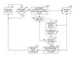
- FIG. 1 illustrates a block diagram of a multi-processor environment communicating over a common bus with a plurality of external devices
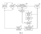
- FIG. 2 illustrates a flowchart of high level decisions of a debug program operating in accordance with one embodiment of the invention
- FIG. 3 illustrates a representative state flow diagram for initiating a debugging operation
- FIG. 4 a representative state flow diagram for terminating debugging operation.
- FIG. 1 disclosed is an exemplary diagram of a multi-processor environment in which a processing unit (PU) 100 represents a main, prime or central processor.
- SPU 102 , SPU 104 and SPU 106 are supplemental processors that work with or assist PU 100 .
- At least one of the additional SPUs, such as SPU 102 can be of the type such that the register states cannot be read by PU 100 over a communication bus 108 .
- Memory 110 , Input/Output (I/O) 112 , disk drive 114 , printer 116 and monitor 118 represent external devices that communicate with at least one of the PUs via bus 108 .
- I/O Input/Output
- debugging programs or tools can be used to examine the contents of various registers in the processor.
- the details of the debugging process are usually obvious and well defined when the processor operating the debugging program is the same processor encountering errors from other programs codes. It is also a reasonably straight-forward and known process to debug a program operating on a limited resource PU using an additional PU. If that subsequent PU has adequate memory resources, the registers of the limited resource PU can be read directly by the subsequent PU if there is an operational interruption of the program debugging process.
- Operational halting can occur by placing temporary stops in the debugging program process, then reading and comparing the contents of the appropriate registers to the data that is expected in those registers at that stage of the program operation. When they differ from expected results, elements of the program code can be changed. The program is recompiled to determine if the new code results in eliminating the bug. Alternatively, the contents of some of the registers can be changed and the program may be allowed to continue to see if there are further problem areas in the code. However, neither of these operations can be accomplished if the PU operating the debug cannot read, on direct command, the contents of the registers of the PU running the program to be debugged.
- FIG. 2 illustrated is a flowchart of high level decisions of a debug program operating in accordance with one embodiment of the invention, such as the processor 100 of FIG. 1 .
- a debugger event loop 200 operates in conjunction with a decision block 202 to detect the occurrence of an inserted command used in the program being debugged, to interrupt the operation of that program.
- the decision ring comprising debugger event loop 200 and program stopped 202 loops continually until the program being debugged stops.
- the debugging program proceeds to a program operation block 204 where a copy program is activated in the limited resource PU under debugging.
- the copy program operates to send a plurality of indicia from the limited resource PU back to the debugging or main PU.
- the data sent back, in accordance with the operator of the debugging program may be limited to the contents of certain registers or may include the entire program and all parameters of the limited resource PU.
- the storage of the data returned is held in storage at register cache 206 .
- the operator of main PU can run the program in memory set aside in local cache.
- the debugging program awaits operator or user input.
- User defined input at block 210 may read from register cache 206 or write to a space representing a register allocated in memory.
- Other user requests block 212 accepts additional inputs to the system.
- a decision block 214 represents a decision by the user to provide more inputs with a return to wait for user input 208 or to restore the modified context data presently in the register cache 206 to a target processor. The target PU restarts because of operation by a restore modified context block 218 and a return is made to debugger event loop 200 . If the program in the process of debugging operates as expected, the debugging process then completes. However, the program may not always show an improper operation, and a further check may need to be made of the register values before determining that the program is operating properly.
- FIG. 3 illustrated is an amplification of the steps required in block 204 of FIG. 2 .
- a portion of main CPU memory 110 from FIG. 1 is allocated to receive the register contents of a auxiliary processor, such as SPU 102 .
- a auxiliary processor such as SPU 102 .
- the stopped operation is detected and verified in condition block 302 .
- a portion of the SPUs local store or memory, illustrated by a sub-block MEM 103 is saved to MEM 110 . This area is reserved in main memory by the debugging program for use by the program being debugged.
- Copy and start block 306 completes its cycle and outputs the copied program to the reserved area of the local store, of the specified processor.
- the deterministic logic waits for the debugging of the program to complete.
- the system waits further instruction from the user input 208 of FIG. 2 .
- FIG. 4 disclosed are the actions of the debugging program as related to the portion of the debugging program activated in the section of memory of the target SPU.
- the copy SPU's registers block 400 copies the selected register data from the SPU 102 into a block reserved memory allocation at MEM 103 .
- command block 402 issues a command to make a copy of the area of MEM 102 holding the present register state and forward that copy to an allocated portion of CPU 100 memory.
- command block 402 copies indicia remaining in MEM 103 , (which is unrelated to the register state) and forwards that copy to CPU 100 .
- MEM 103 contains the salient data that causes the program halt. There can be additional code lines in MEM 103 , which may be related or unrelated to the debugging operation.
Abstract
Description
- This application is a continuation of, and claims the benefit of the filing date of, co-pending U.S. patent application Ser. No. 10/697,865 entitled PROGRAM DEBUG METHOD AND APPARATUS filed Oct. 30, 2003.
- The present invention relates generally to the field of processor operations and, more particularly, to debugging a program on a limited resources processor.
- Normally, a program is debugged (errors found and eliminated) on a central processing unit, (CPU) or other processing units (PU) that the program is designed to run on. However when a plurality of PUs are placed on a single chip, it is sometimes desirable to limit the memory available to one or more specialized function processing units (SPUs). At that point, the supplemental processor processes those tasks with its highest efficiency. With this methodology, the number of possible PUs placed on a specified size chip is increased
- In a conventional system, a debugger will have unlimited access to all of the states in the executable program that is being debugged. The debugger needs to issue read and write commands to a plurality of addresses. Subsequently, the debugger logic modifies the states of executable operations. If the memory or flexibility of the PU is limited, reads and writes may not be possible even if the debugging program employs a master, main or control PU. Furthermore, in order to maximize processing power for specified chip architecture, the main or control PU may not have access to the register state of the SPUs on the chip.
- Accordingly, a need exists for a system that efficiently and effectively reduces such problems by developing a procedure to debug a program designed to run on a SPU having limited resources and which does not allow SPU register state access to devices external to the SPU.
- The present invention provides for installing a retrieval program on an SPU having a program needing debugging. The register states deploy to a primary processing unit that performs the debugging process in a pool of memory.
- For a more complete understanding of the present invention, and the advantages thereof, reference is now made to the following Detailed Description taken in conjunction with the accompanying drawings, in which:
-
FIG. 1 illustrates a block diagram of a multi-processor environment communicating over a common bus with a plurality of external devices; -
FIG. 2 illustrates a flowchart of high level decisions of a debug program operating in accordance with one embodiment of the invention; -
FIG. 3 illustrates a representative state flow diagram for initiating a debugging operation; and -
FIG. 4 a representative state flow diagram for terminating debugging operation. - In the following discussion, numerous specific details are set forth to provide a thorough understanding of the present invention. However, those skilled in the art will appreciate that the present invention may be practiced without such specific details. In other instances, well-known elements have been illustrated in schematic or block diagram form in order not to obscure the present invention in unnecessary detail. Additionally, for the most part, details concerning network communications, electromagnetic signaling techniques, and the like, have been omitted inasmuch as such details are not considered necessary to obtain a complete understanding of the present invention, and are considered to be within the understanding of persons of ordinary skill in the relevant art.
- It is further noted that, unless indicated otherwise, all functions described herein may be performed in either hardware or software, or some combination thereof. In one embodiment, however, the functions are performed by a processor, such as a computer or an electronic data processor, in accordance with code, such as computer program code, software, and/or integrated circuits that are coded to perform such functions, unless indicated otherwise.
- Turning to
FIG. 1 , disclosed is an exemplary diagram of a multi-processor environment in which a processing unit (PU) 100 represents a main, prime or central processor. SPU 102, SPU 104 and SPU 106 are supplemental processors that work with or assistPU 100. At least one of the additional SPUs, such asSPU 102, can be of the type such that the register states cannot be read byPU 100 over acommunication bus 108. There are significant purposes for eliminating the ability of other processors reading the register states of interconnected PUs. For example, the need to reduce device complexity and for increasing the number of PUs that can be accommodated within a specified device architecture.Memory 110, Input/Output (I/O) 112,disk drive 114,printer 116 andmonitor 118 represent external devices that communicate with at least one of the PUs viabus 108. - As is known to those skilled in the art of coding software, programs do not always work as expected. In diagnosing the reasons for faulty or erroneous operations, “debugging” programs or tools can be used to examine the contents of various registers in the processor. The details of the debugging process are usually obvious and well defined when the processor operating the debugging program is the same processor encountering errors from other programs codes. It is also a reasonably straight-forward and known process to debug a program operating on a limited resource PU using an additional PU. If that subsequent PU has adequate memory resources, the registers of the limited resource PU can be read directly by the subsequent PU if there is an operational interruption of the program debugging process.
- Operational halting can occur by placing temporary stops in the debugging program process, then reading and comparing the contents of the appropriate registers to the data that is expected in those registers at that stage of the program operation. When they differ from expected results, elements of the program code can be changed. The program is recompiled to determine if the new code results in eliminating the bug. Alternatively, the contents of some of the registers can be changed and the program may be allowed to continue to see if there are further problem areas in the code. However, neither of these operations can be accomplished if the PU operating the debug cannot read, on direct command, the contents of the registers of the PU running the program to be debugged.
- Turning to
FIG. 2 , illustrated is a flowchart of high level decisions of a debug program operating in accordance with one embodiment of the invention, such as theprocessor 100 ofFIG. 1 . - A
debugger event loop 200 operates in conjunction with adecision block 202 to detect the occurrence of an inserted command used in the program being debugged, to interrupt the operation of that program. The decision ring comprisingdebugger event loop 200 and program stopped 202 loops continually until the program being debugged stops. At that time, the debugging program proceeds to aprogram operation block 204 where a copy program is activated in the limited resource PU under debugging. The copy program operates to send a plurality of indicia from the limited resource PU back to the debugging or main PU. The data sent back, in accordance with the operator of the debugging program may be limited to the contents of certain registers or may include the entire program and all parameters of the limited resource PU. The storage of the data returned is held in storage atregister cache 206. The operator of main PU can run the program in memory set aside in local cache. - As shown by the wait for
user input 208 block, after the data is stored or placed in memory, the debugging program awaits operator or user input. User defined input atblock 210, may read fromregister cache 206 or write to a space representing a register allocated in memory. Otheruser requests block 212 accepts additional inputs to the system. Adecision block 214 represents a decision by the user to provide more inputs with a return to wait foruser input 208 or to restore the modified context data presently in theregister cache 206 to a target processor. The target PU restarts because of operation by a restore modifiedcontext block 218 and a return is made to debuggerevent loop 200. If the program in the process of debugging operates as expected, the debugging process then completes. However, the program may not always show an improper operation, and a further check may need to be made of the register values before determining that the program is operating properly. - Turning to
FIG. 3 , illustrated is an amplification of the steps required inblock 204 ofFIG. 2 . A portion ofmain CPU memory 110 fromFIG. 1 is allocated to receive the register contents of a auxiliary processor, such as SPU 102. When the program under debugging inPU 102, has stopped due to operational interrupts, the stopped operation is detected and verified incondition block 302. A portion of the SPUs local store or memory, illustrated by asub-block MEM 103, is saved toMEM 110. This area is reserved in main memory by the debugging program for use by the program being debugged. - Copy and start block 306 completes its cycle and outputs the copied program to the reserved area of the local store, of the specified processor. At a
wait state block 308, the deterministic logic waits for the debugging of the program to complete. At the conclusion of the processing, the system waits further instruction from theuser input 208 ofFIG. 2 . - Turning now to
FIG. 4 , disclosed are the actions of the debugging program as related to the portion of the debugging program activated in the section of memory of the target SPU. After activation of the debugging call fromdebugger event loop 200 inFIG. 1 , the copy SPU's registers block 400, copies the selected register data from theSPU 102 into a block reserved memory allocation atMEM 103. Next, command block 402 issues a command to make a copy of the area ofMEM 102 holding the present register state and forward that copy to an allocated portion ofCPU 100 memory. Concurrently, command block 402 copies indicia remaining inMEM 103, (which is unrelated to the register state) and forwards that copy toCPU 100. At a minimum,MEM 103 contains the salient data that causes the program halt. There can be additional code lines inMEM 103, which may be related or unrelated to the debugging operation. When the processing ofcommand block 404 is complete, and output is sent to signalcompletion block 406, thedebugger event loop 200 resets and waits for a subsequent program halt instruction. - It is understood that the present invention can take many forms and implementations. Accordingly, several variations may be made in the foregoing without departing from the spirit or the scope of the invention. The capabilities outlined herein allow for the possibility of a variety of design and programming models. This disclosure should not be read as preferring any particular design or programming model, but is instead directed to the underlying mechanisms on which these design and programming models can be built.
- Having thus described the present invention by reference to certain of its salient characteristics, it is noted that the features disclosed are illustrative rather than limiting in nature. A wide range of variations, modifications, changes, and substitutions are contemplated in the foregoing disclosure and, in some instances, some features of the present invention may be employed without a corresponding use of the other features. Many such variations and modifications may be considered desirable by those skilled in the art based on a review of the foregoing description. Accordingly, it is appropriate that the appended claims be construed broadly and in a manner consistent with the scope of the invention.
Claims (6)
Priority Applications (1)
| Application Number | Priority Date | Filing Date | Title |
|---|---|---|---|
| US11/959,998 US7669078B2 (en) | 2003-10-30 | 2007-12-19 | Method and apparatus for debugging a program on a limited resource processor |
Applications Claiming Priority (2)
| Application Number | Priority Date | Filing Date | Title |
|---|---|---|---|
| US10/697,865 US7363544B2 (en) | 2003-10-30 | 2003-10-30 | Program debug method and apparatus |
| US11/959,998 US7669078B2 (en) | 2003-10-30 | 2007-12-19 | Method and apparatus for debugging a program on a limited resource processor |
Related Parent Applications (1)
| Application Number | Title | Priority Date | Filing Date |
|---|---|---|---|
| US10/697,865 Continuation US7363544B2 (en) | 2003-10-30 | 2003-10-30 | Program debug method and apparatus |
Publications (2)
| Publication Number | Publication Date |
|---|---|
| US20080098264A1 true US20080098264A1 (en) | 2008-04-24 |
| US7669078B2 US7669078B2 (en) | 2010-02-23 |
Family
ID=34550472
Family Applications (2)
| Application Number | Title | Priority Date | Filing Date |
|---|---|---|---|
| US10/697,865 Active - Reinstated 2025-08-21 US7363544B2 (en) | 2003-10-30 | 2003-10-30 | Program debug method and apparatus |
| US11/959,998 Expired - Lifetime US7669078B2 (en) | 2003-10-30 | 2007-12-19 | Method and apparatus for debugging a program on a limited resource processor |
Family Applications Before (1)
| Application Number | Title | Priority Date | Filing Date |
|---|---|---|---|
| US10/697,865 Active - Reinstated 2025-08-21 US7363544B2 (en) | 2003-10-30 | 2003-10-30 | Program debug method and apparatus |
Country Status (1)
| Country | Link |
|---|---|
| US (2) | US7363544B2 (en) |
Cited By (6)
| Publication number | Priority date | Publication date | Assignee | Title |
|---|---|---|---|---|
| US20070245313A1 (en) * | 2006-04-14 | 2007-10-18 | Microsoft Corporation | Failure tagging |
| US20080184079A1 (en) * | 2007-01-31 | 2008-07-31 | Microsoft Corporation | Tracking down elusive intermittent failures |
| US20080184075A1 (en) * | 2007-01-31 | 2008-07-31 | Microsoft Corporation | Break and optional hold on failure |
| WO2017063529A1 (en) * | 2015-10-16 | 2017-04-20 | 华为技术有限公司 | Method and apparatus for executing non-maskable interrupt |
| CN108616366A (en) * | 2016-12-09 | 2018-10-02 | 华为技术有限公司 | service processing unit management method and device |
| US10366153B2 (en) | 2003-03-12 | 2019-07-30 | Microsoft Technology Licensing, Llc | System and method for customizing note flags |
Families Citing this family (15)
| Publication number | Priority date | Publication date | Assignee | Title |
|---|---|---|---|---|
| US20050278517A1 (en) * | 2004-05-19 | 2005-12-15 | Kar-Lik Wong | Systems and methods for performing branch prediction in a variable length instruction set microprocessor |
| US7587635B2 (en) * | 2004-10-04 | 2009-09-08 | Cisco Technology, Inc. | Method of debugging “active” unit using “non-intrusive source-level debugger” on “standby” unit of high availability system |
| US7793160B1 (en) * | 2005-03-29 | 2010-09-07 | Emc Corporation | Systems and methods for tracing errors |
| US20060235655A1 (en) * | 2005-04-18 | 2006-10-19 | Qing Richard X | Method for monitoring function execution |
| US20060259692A1 (en) * | 2005-05-16 | 2006-11-16 | Texas Instruments Incorporated | Writing to a specified cache |
| US20060288332A1 (en) * | 2005-06-21 | 2006-12-21 | Microsoft Corporation | Workflow debugger |
| US20070073925A1 (en) * | 2005-09-28 | 2007-03-29 | Arc International (Uk) Limited | Systems and methods for synchronizing multiple processing engines of a microprocessor |
| JP4222370B2 (en) * | 2006-01-11 | 2009-02-12 | セイコーエプソン株式会社 | Program for causing a computer to execute a debugging support apparatus and a debugging processing method |
| US7882399B2 (en) * | 2007-12-13 | 2011-02-01 | International Business Machines Corporation | Intelligent job functionality |
| US8719797B2 (en) | 2010-05-18 | 2014-05-06 | Blackberry Limited | System and method for debugging dynamically generated code of an application |
| US9135161B2 (en) | 2012-06-12 | 2015-09-15 | International Business Machines Corporation | Flash translation layer system for maintaining data versions in solid state memory |
| US9122581B2 (en) | 2012-06-12 | 2015-09-01 | International Business Machines Corporation | Data versioning in solid state memory |
| US9116793B2 (en) * | 2012-06-12 | 2015-08-25 | International Business Machines Corporation | Maintaining versions of data in solid state memory |
| US9122582B2 (en) | 2012-06-12 | 2015-09-01 | International Business Machines Corporation | File system for maintaining data versions in solid state memory |
| CN116594700B (en) * | 2023-07-17 | 2023-12-12 | 合肥康芯威存储技术有限公司 | Method and device for cloning eMMC chip, electronic equipment and storage medium |
Citations (20)
| Publication number | Priority date | Publication date | Assignee | Title |
|---|---|---|---|---|
| US662549A (en) * | 1900-06-23 | 1900-11-27 | Charles C Gardiner | Semaphore-operating mechanism. |
| US3818458A (en) * | 1972-11-08 | 1974-06-18 | Comress | Method and apparatus for monitoring a general purpose digital computer |
| US4819234A (en) * | 1987-05-01 | 1989-04-04 | Prime Computer, Inc. | Operating system debugger |
| US5491787A (en) * | 1994-08-25 | 1996-02-13 | Unisys Corporation | Fault tolerant digital computer system having two processors which periodically alternate as master and slave |
| US5519715A (en) * | 1995-01-27 | 1996-05-21 | Sun Microsystems, Inc. | Full-speed microprocessor testing employing boundary scan |
| US5533192A (en) * | 1994-04-21 | 1996-07-02 | Apple Computer, Inc. | Computer program debugging system and method |
| US5581695A (en) * | 1990-05-09 | 1996-12-03 | Applied Microsystems Corporation | Source-level run-time software code debugging instrument |
| US5615331A (en) * | 1994-06-23 | 1997-03-25 | Phoenix Technologies Ltd. | System and method for debugging a computing system |
| US6119246A (en) * | 1997-03-31 | 2000-09-12 | International Business Machines Corporation | Error collection coordination for software-readable and non-software readable fault isolation registers in a computer system |
| US6356960B1 (en) * | 1997-10-29 | 2002-03-12 | Sgs-Thomson Microelectronics Limited | Microprocessor having an on-chip CPU fetching a debugging routine from a memory in an external debugging device in response to a control signal received through a debugging port |
| US6484274B1 (en) * | 1996-09-16 | 2002-11-19 | Advanced Micro Devices, Inc. | Method for identifying and correcting error in a central processing unit |
| US20040207630A1 (en) * | 2003-04-21 | 2004-10-21 | Moreton Henry P. | System and method for reserving and managing memory spaces in a memory resource |
| US6820192B2 (en) * | 2000-07-05 | 2004-11-16 | Advanced Digital Chips Inc. | Central processing unit for easily testing and debugging programs |
| US6845470B2 (en) * | 2002-02-27 | 2005-01-18 | International Business Machines Corporation | Method and system to identify a memory corruption source within a multiprocessor system |
| US6857084B1 (en) * | 2001-08-06 | 2005-02-15 | Lsi Logic Corporation | Multiprocessor system and method for simultaneously placing all processors into debug mode |
| US6859891B2 (en) * | 1999-10-01 | 2005-02-22 | Stmicroelectronics Limited | Apparatus and method for shadowing processor information |
| US6925584B2 (en) * | 1999-12-13 | 2005-08-02 | Intel Corporation | Systems and methods for testing processors |
| US7100033B2 (en) * | 2002-10-23 | 2006-08-29 | Intel Corporation | Controlling the timing of test modes in a multiple processor system |
| US7111200B2 (en) * | 2003-04-17 | 2006-09-19 | International Business Machines Corporation | Apparatus and method for debugging a logical partition |
| US7124404B1 (en) * | 2000-05-16 | 2006-10-17 | Mindspeed Technologies, Inc. | Method and system for debugging multiprocessor systems |
Family Cites Families (1)
| Publication number | Priority date | Publication date | Assignee | Title |
|---|---|---|---|---|
| US6625749B1 (en) * | 1999-12-21 | 2003-09-23 | Intel Corporation | Firmware mechanism for correcting soft errors |
-
2003
- 2003-10-30 US US10/697,865 patent/US7363544B2/en active Active - Reinstated
-
2007
- 2007-12-19 US US11/959,998 patent/US7669078B2/en not_active Expired - Lifetime
Patent Citations (20)
| Publication number | Priority date | Publication date | Assignee | Title |
|---|---|---|---|---|
| US662549A (en) * | 1900-06-23 | 1900-11-27 | Charles C Gardiner | Semaphore-operating mechanism. |
| US3818458A (en) * | 1972-11-08 | 1974-06-18 | Comress | Method and apparatus for monitoring a general purpose digital computer |
| US4819234A (en) * | 1987-05-01 | 1989-04-04 | Prime Computer, Inc. | Operating system debugger |
| US5581695A (en) * | 1990-05-09 | 1996-12-03 | Applied Microsystems Corporation | Source-level run-time software code debugging instrument |
| US5533192A (en) * | 1994-04-21 | 1996-07-02 | Apple Computer, Inc. | Computer program debugging system and method |
| US5615331A (en) * | 1994-06-23 | 1997-03-25 | Phoenix Technologies Ltd. | System and method for debugging a computing system |
| US5491787A (en) * | 1994-08-25 | 1996-02-13 | Unisys Corporation | Fault tolerant digital computer system having two processors which periodically alternate as master and slave |
| US5519715A (en) * | 1995-01-27 | 1996-05-21 | Sun Microsystems, Inc. | Full-speed microprocessor testing employing boundary scan |
| US6484274B1 (en) * | 1996-09-16 | 2002-11-19 | Advanced Micro Devices, Inc. | Method for identifying and correcting error in a central processing unit |
| US6119246A (en) * | 1997-03-31 | 2000-09-12 | International Business Machines Corporation | Error collection coordination for software-readable and non-software readable fault isolation registers in a computer system |
| US6356960B1 (en) * | 1997-10-29 | 2002-03-12 | Sgs-Thomson Microelectronics Limited | Microprocessor having an on-chip CPU fetching a debugging routine from a memory in an external debugging device in response to a control signal received through a debugging port |
| US6859891B2 (en) * | 1999-10-01 | 2005-02-22 | Stmicroelectronics Limited | Apparatus and method for shadowing processor information |
| US6925584B2 (en) * | 1999-12-13 | 2005-08-02 | Intel Corporation | Systems and methods for testing processors |
| US7124404B1 (en) * | 2000-05-16 | 2006-10-17 | Mindspeed Technologies, Inc. | Method and system for debugging multiprocessor systems |
| US6820192B2 (en) * | 2000-07-05 | 2004-11-16 | Advanced Digital Chips Inc. | Central processing unit for easily testing and debugging programs |
| US6857084B1 (en) * | 2001-08-06 | 2005-02-15 | Lsi Logic Corporation | Multiprocessor system and method for simultaneously placing all processors into debug mode |
| US6845470B2 (en) * | 2002-02-27 | 2005-01-18 | International Business Machines Corporation | Method and system to identify a memory corruption source within a multiprocessor system |
| US7100033B2 (en) * | 2002-10-23 | 2006-08-29 | Intel Corporation | Controlling the timing of test modes in a multiple processor system |
| US7111200B2 (en) * | 2003-04-17 | 2006-09-19 | International Business Machines Corporation | Apparatus and method for debugging a logical partition |
| US20040207630A1 (en) * | 2003-04-21 | 2004-10-21 | Moreton Henry P. | System and method for reserving and managing memory spaces in a memory resource |
Cited By (12)
| Publication number | Priority date | Publication date | Assignee | Title |
|---|---|---|---|---|
| US10366153B2 (en) | 2003-03-12 | 2019-07-30 | Microsoft Technology Licensing, Llc | System and method for customizing note flags |
| US20070245313A1 (en) * | 2006-04-14 | 2007-10-18 | Microsoft Corporation | Failure tagging |
| US20080184079A1 (en) * | 2007-01-31 | 2008-07-31 | Microsoft Corporation | Tracking down elusive intermittent failures |
| US20080184075A1 (en) * | 2007-01-31 | 2008-07-31 | Microsoft Corporation | Break and optional hold on failure |
| US7673178B2 (en) * | 2007-01-31 | 2010-03-02 | Microsoft Corporation | Break and optional hold on failure |
| US7788540B2 (en) | 2007-01-31 | 2010-08-31 | Microsoft Corporation | Tracking down elusive intermittent failures |
| WO2017063529A1 (en) * | 2015-10-16 | 2017-04-20 | 华为技术有限公司 | Method and apparatus for executing non-maskable interrupt |
| US20180225143A1 (en) * | 2015-10-16 | 2018-08-09 | Huawei Technologies Co., Ltd. | Method and apparatus for executing non-maskable interrupt |
| US10437632B2 (en) * | 2015-10-16 | 2019-10-08 | Huawei Technologies Co., Ltd. | Method and apparatus for executing non-maskable interrupt |
| US10970108B2 (en) | 2015-10-16 | 2021-04-06 | Huawei Technologies Co., Ltd. | Method and apparatus for executing non-maskable interrupt |
| US11360803B2 (en) | 2015-10-16 | 2022-06-14 | Huawei Technologies Co., Ltd. | Method and apparatus for executing non-maskable interrupt |
| CN108616366A (en) * | 2016-12-09 | 2018-10-02 | 华为技术有限公司 | service processing unit management method and device |
Also Published As
| Publication number | Publication date |
|---|---|
| US7363544B2 (en) | 2008-04-22 |
| US20050097398A1 (en) | 2005-05-05 |
| US7669078B2 (en) | 2010-02-23 |
Similar Documents
| Publication | Publication Date | Title |
|---|---|---|
| US7669078B2 (en) | Method and apparatus for debugging a program on a limited resource processor | |
| US7577874B2 (en) | Interactive debug system for multiprocessor array | |
| US8495344B2 (en) | Simultaneous execution resumption of multiple processor cores after core state information dump to facilitate debugging via multi-core processor simulator using the state information | |
| JP2005129053A (en) | Fault-tolerant multi-core microprocessing | |
| CN112015599B (en) | Method and apparatus for error recovery | |
| US6779132B2 (en) | Preserving dump capability after a fault-on-fault or related type failure in a fault tolerant computer system | |
| US9372702B2 (en) | Non-disruptive code update of a single processor in a multi-processor computing system | |
| US7966536B2 (en) | Method and apparatus for automatic scan completion in the event of a system checkstop | |
| US4355389A (en) | Microprogrammed information processing system having self-checking function | |
| JPH0689201A (en) | Microprocessor having run/stop pin for accessing idle mode and operating method thereof | |
| US6968410B2 (en) | Multi-threaded processing of system management interrupts | |
| US7203819B2 (en) | Program processing device | |
| CN104346306A (en) | System and method of high integrity DMA operation | |
| JPH07141176A (en) | Command retrial control system | |
| US7617417B2 (en) | Method for reading input/output port data | |
| JP2005332030A (en) | Controller | |
| US10592329B2 (en) | Method and electronic device for continuing executing procedure being aborted from physical address where error occurs | |
| Floridia et al. | Parallel software-based self-test suite for multi-core system-on-chip: Migration from single-core to multi-core automotive microcontrollers | |
| JP2002229811A (en) | Control method of logical partition system | |
| JP2008140124A (en) | Data processor | |
| JP4853620B2 (en) | Multiprocessor system and initial startup method and program | |
| US7225284B2 (en) | Increasing the quantity of I/O decode ranges using SMI traps | |
| Angione et al. | Online scheduling of concurrent memory bists execution at real-time operating-system level | |
| TWI663544B (en) | Fault tolerant operating metohd and electronic device using the same | |
| JPS60142747A (en) | Instruction execution control system |
Legal Events
| Date | Code | Title | Description |
|---|---|---|---|
| FEPP | Fee payment procedure |
Free format text: PAYOR NUMBER ASSIGNED (ORIGINAL EVENT CODE: ASPN); ENTITY STATUS OF PATENT OWNER: LARGE ENTITY |
|
| STCF | Information on status: patent grant |
Free format text: PATENTED CASE |
|
| AS | Assignment |
Owner name: FACEBOOK, INC., CALIFORNIA Free format text: ASSIGNMENT OF ASSIGNORS INTEREST;ASSIGNOR:INTERNATIONAL BUSINESS MACHINES CORPORATION;REEL/FRAME:027988/0806 Effective date: 20120327 |
|
| FPAY | Fee payment |
Year of fee payment: 4 |
|
| FPAY | Fee payment |
Year of fee payment: 8 |
|
| MAFP | Maintenance fee payment |
Free format text: PAYMENT OF MAINTENANCE FEE, 12TH YEAR, LARGE ENTITY (ORIGINAL EVENT CODE: M1553); ENTITY STATUS OF PATENT OWNER: LARGE ENTITY Year of fee payment: 12 |
|
| AS | Assignment |
Owner name: META PLATFORMS, INC., CALIFORNIA Free format text: CHANGE OF NAME;ASSIGNOR:FACEBOOK, INC.;REEL/FRAME:058553/0802 Effective date: 20211028 |