US20110217841A1 - Method of forming through silicon via with dummy structure - Google Patents
Method of forming through silicon via with dummy structure Download PDFInfo
- Publication number
- US20110217841A1 US20110217841A1 US13/112,347 US201113112347A US2011217841A1 US 20110217841 A1 US20110217841 A1 US 20110217841A1 US 201113112347 A US201113112347 A US 201113112347A US 2011217841 A1 US2011217841 A1 US 2011217841A1
- Authority
- US
- United States
- Prior art keywords
- forming
- interconnect
- pad
- layer
- conductive post
- Prior art date
- Legal status (The legal status is an assumption and is not a legal conclusion. Google has not performed a legal analysis and makes no representation as to the accuracy of the status listed.)
- Granted
Links
- 238000000034 method Methods 0.000 title claims abstract description 56
- 239000010703 silicon Substances 0.000 title claims abstract description 26
- 229910052710 silicon Inorganic materials 0.000 title claims abstract description 24
- 239000000758 substrate Substances 0.000 claims abstract description 50
- 238000002161 passivation Methods 0.000 claims description 25
- 238000002955 isolation Methods 0.000 claims description 15
- 238000005530 etching Methods 0.000 claims description 8
- PXHVJJICTQNCMI-UHFFFAOYSA-N Nickel Chemical compound [Ni] PXHVJJICTQNCMI-UHFFFAOYSA-N 0.000 claims description 6
- 238000005498 polishing Methods 0.000 claims description 5
- PCHJSUWPFVWCPO-UHFFFAOYSA-N gold Chemical compound [Au] PCHJSUWPFVWCPO-UHFFFAOYSA-N 0.000 claims description 3
- 229910052737 gold Inorganic materials 0.000 claims description 3
- 239000010931 gold Substances 0.000 claims description 3
- 238000007654 immersion Methods 0.000 claims description 3
- 229910052759 nickel Inorganic materials 0.000 claims description 3
- 230000015572 biosynthetic process Effects 0.000 claims description 2
- 238000009827 uniform distribution Methods 0.000 claims 1
- 239000010410 layer Substances 0.000 description 73
- 239000010949 copper Substances 0.000 description 20
- 229910052751 metal Inorganic materials 0.000 description 20
- 239000002184 metal Substances 0.000 description 20
- XUIMIQQOPSSXEZ-UHFFFAOYSA-N Silicon Chemical compound [Si] XUIMIQQOPSSXEZ-UHFFFAOYSA-N 0.000 description 19
- 229910052802 copper Inorganic materials 0.000 description 17
- RYGMFSIKBFXOCR-UHFFFAOYSA-N Copper Chemical compound [Cu] RYGMFSIKBFXOCR-UHFFFAOYSA-N 0.000 description 15
- 229910052782 aluminium Inorganic materials 0.000 description 15
- XAGFODPZIPBFFR-UHFFFAOYSA-N aluminium Chemical compound [Al] XAGFODPZIPBFFR-UHFFFAOYSA-N 0.000 description 14
- 229910021332 silicide Inorganic materials 0.000 description 14
- FVBUAEGBCNSCDD-UHFFFAOYSA-N silicide(4-) Chemical compound [Si-4] FVBUAEGBCNSCDD-UHFFFAOYSA-N 0.000 description 14
- 229920002120 photoresistant polymer Polymers 0.000 description 13
- VYPSYNLAJGMNEJ-UHFFFAOYSA-N Silicium dioxide Chemical compound O=[Si]=O VYPSYNLAJGMNEJ-UHFFFAOYSA-N 0.000 description 11
- 239000000463 material Substances 0.000 description 11
- 239000003989 dielectric material Substances 0.000 description 10
- 238000004519 manufacturing process Methods 0.000 description 9
- 238000005240 physical vapour deposition Methods 0.000 description 9
- 239000004065 semiconductor Substances 0.000 description 9
- 235000012431 wafers Nutrition 0.000 description 9
- 238000005229 chemical vapour deposition Methods 0.000 description 8
- WFKWXMTUELFFGS-UHFFFAOYSA-N tungsten Chemical compound [W] WFKWXMTUELFFGS-UHFFFAOYSA-N 0.000 description 7
- 229910052721 tungsten Inorganic materials 0.000 description 7
- 239000010937 tungsten Substances 0.000 description 7
- 229910052581 Si3N4 Inorganic materials 0.000 description 6
- HQVNEWCFYHHQES-UHFFFAOYSA-N silicon nitride Chemical compound N12[Si]34N5[Si]62N3[Si]51N64 HQVNEWCFYHHQES-UHFFFAOYSA-N 0.000 description 6
- 229910052814 silicon oxide Inorganic materials 0.000 description 6
- 238000004544 sputter deposition Methods 0.000 description 6
- 229910021420 polycrystalline silicon Inorganic materials 0.000 description 5
- 229920005591 polysilicon Polymers 0.000 description 5
- 239000010936 titanium Substances 0.000 description 5
- 229910052719 titanium Inorganic materials 0.000 description 5
- 229910000881 Cu alloy Inorganic materials 0.000 description 4
- KDLHZDBZIXYQEI-UHFFFAOYSA-N Palladium Chemical compound [Pd] KDLHZDBZIXYQEI-UHFFFAOYSA-N 0.000 description 4
- RTAQQCXQSZGOHL-UHFFFAOYSA-N Titanium Chemical compound [Ti] RTAQQCXQSZGOHL-UHFFFAOYSA-N 0.000 description 4
- NRTOMJZYCJJWKI-UHFFFAOYSA-N Titanium nitride Chemical compound [Ti]#N NRTOMJZYCJJWKI-UHFFFAOYSA-N 0.000 description 4
- 239000004020 conductor Substances 0.000 description 4
- 238000007747 plating Methods 0.000 description 4
- 229910052715 tantalum Inorganic materials 0.000 description 4
- GUVRBAGPIYLISA-UHFFFAOYSA-N tantalum atom Chemical compound [Ta] GUVRBAGPIYLISA-UHFFFAOYSA-N 0.000 description 4
- VZGDMQKNWNREIO-UHFFFAOYSA-N tetrachloromethane Chemical compound ClC(Cl)(Cl)Cl VZGDMQKNWNREIO-UHFFFAOYSA-N 0.000 description 4
- 238000005516 engineering process Methods 0.000 description 3
- 239000010408 film Substances 0.000 description 3
- 239000000203 mixture Substances 0.000 description 3
- 238000001020 plasma etching Methods 0.000 description 3
- ZXEYZECDXFPJRJ-UHFFFAOYSA-N $l^{3}-silane;platinum Chemical compound [SiH3].[Pt] ZXEYZECDXFPJRJ-UHFFFAOYSA-N 0.000 description 2
- 229910016570 AlCu Inorganic materials 0.000 description 2
- 206010010144 Completed suicide Diseases 0.000 description 2
- 229910052691 Erbium Inorganic materials 0.000 description 2
- XPDWGBQVDMORPB-UHFFFAOYSA-N Fluoroform Chemical compound FC(F)F XPDWGBQVDMORPB-UHFFFAOYSA-N 0.000 description 2
- 229910000676 Si alloy Inorganic materials 0.000 description 2
- 229910000577 Silicon-germanium Inorganic materials 0.000 description 2
- BOTDANWDWHJENH-UHFFFAOYSA-N Tetraethyl orthosilicate Chemical compound CCO[Si](OCC)(OCC)OCC BOTDANWDWHJENH-UHFFFAOYSA-N 0.000 description 2
- LEVVHYCKPQWKOP-UHFFFAOYSA-N [Si].[Ge] Chemical compound [Si].[Ge] LEVVHYCKPQWKOP-UHFFFAOYSA-N 0.000 description 2
- 238000000137 annealing Methods 0.000 description 2
- QVGXLLKOCUKJST-UHFFFAOYSA-N atomic oxygen Chemical compound [O] QVGXLLKOCUKJST-UHFFFAOYSA-N 0.000 description 2
- 229910017052 cobalt Inorganic materials 0.000 description 2
- 239000010941 cobalt Substances 0.000 description 2
- GUTLYIVDDKVIGB-UHFFFAOYSA-N cobalt atom Chemical compound [Co] GUTLYIVDDKVIGB-UHFFFAOYSA-N 0.000 description 2
- UYAHIZSMUZPPFV-UHFFFAOYSA-N erbium Chemical compound [Er] UYAHIZSMUZPPFV-UHFFFAOYSA-N 0.000 description 2
- 239000012530 fluid Substances 0.000 description 2
- 239000011521 glass Substances 0.000 description 2
- 238000003384 imaging method Methods 0.000 description 2
- 239000007788 liquid Substances 0.000 description 2
- RUFLMLWJRZAWLJ-UHFFFAOYSA-N nickel silicide Chemical compound [Ni]=[Si]=[Ni] RUFLMLWJRZAWLJ-UHFFFAOYSA-N 0.000 description 2
- 229910021334 nickel silicide Inorganic materials 0.000 description 2
- 239000001301 oxygen Substances 0.000 description 2
- 229910052760 oxygen Inorganic materials 0.000 description 2
- 229910052763 palladium Inorganic materials 0.000 description 2
- 238000000206 photolithography Methods 0.000 description 2
- 229910021339 platinum silicide Inorganic materials 0.000 description 2
- 239000000377 silicon dioxide Substances 0.000 description 2
- 235000012239 silicon dioxide Nutrition 0.000 description 2
- 238000004528 spin coating Methods 0.000 description 2
- 230000035882 stress Effects 0.000 description 2
- 239000000126 substance Substances 0.000 description 2
- MZLGASXMSKOWSE-UHFFFAOYSA-N tantalum nitride Chemical compound [Ta]#N MZLGASXMSKOWSE-UHFFFAOYSA-N 0.000 description 2
- 229910021341 titanium silicide Inorganic materials 0.000 description 2
- LXEXBJXDGVGRAR-UHFFFAOYSA-N trichloro(trichlorosilyl)silane Chemical compound Cl[Si](Cl)(Cl)[Si](Cl)(Cl)Cl LXEXBJXDGVGRAR-UHFFFAOYSA-N 0.000 description 2
- WQJQOUPTWCFRMM-UHFFFAOYSA-N tungsten disilicide Chemical compound [Si]#[W]#[Si] WQJQOUPTWCFRMM-UHFFFAOYSA-N 0.000 description 2
- 229910021342 tungsten silicide Inorganic materials 0.000 description 2
- JBRZTFJDHDCESZ-UHFFFAOYSA-N AsGa Chemical compound [As]#[Ga] JBRZTFJDHDCESZ-UHFFFAOYSA-N 0.000 description 1
- OKTJSMMVPCPJKN-UHFFFAOYSA-N Carbon Chemical compound [C] OKTJSMMVPCPJKN-UHFFFAOYSA-N 0.000 description 1
- ZAMOUSCENKQFHK-UHFFFAOYSA-N Chlorine atom Chemical compound [Cl] ZAMOUSCENKQFHK-UHFFFAOYSA-N 0.000 description 1
- PXGOKWXKJXAPGV-UHFFFAOYSA-N Fluorine Chemical compound FF PXGOKWXKJXAPGV-UHFFFAOYSA-N 0.000 description 1
- 229910000673 Indium arsenide Inorganic materials 0.000 description 1
- GPXJNWSHGFTCBW-UHFFFAOYSA-N Indium phosphide Chemical compound [In]#P GPXJNWSHGFTCBW-UHFFFAOYSA-N 0.000 description 1
- 239000004642 Polyimide Substances 0.000 description 1
- ATJFFYVFTNAWJD-UHFFFAOYSA-N Tin Chemical compound [Sn] ATJFFYVFTNAWJD-UHFFFAOYSA-N 0.000 description 1
- 239000004964 aerogel Substances 0.000 description 1
- 230000004075 alteration Effects 0.000 description 1
- 238000004380 ashing Methods 0.000 description 1
- 229910052799 carbon Inorganic materials 0.000 description 1
- 229910052801 chlorine Inorganic materials 0.000 description 1
- 239000000460 chlorine Substances 0.000 description 1
- 239000011248 coating agent Substances 0.000 description 1
- 238000000576 coating method Methods 0.000 description 1
- 230000000295 complement effect Effects 0.000 description 1
- 150000001875 compounds Chemical class 0.000 description 1
- 230000032798 delamination Effects 0.000 description 1
- 239000010432 diamond Substances 0.000 description 1
- BUMGIEFFCMBQDG-UHFFFAOYSA-N dichlorosilicon Chemical compound Cl[Si]Cl BUMGIEFFCMBQDG-UHFFFAOYSA-N 0.000 description 1
- PZPGRFITIJYNEJ-UHFFFAOYSA-N disilane Chemical compound [SiH3][SiH3] PZPGRFITIJYNEJ-UHFFFAOYSA-N 0.000 description 1
- 230000005669 field effect Effects 0.000 description 1
- 238000011049 filling Methods 0.000 description 1
- 229910052731 fluorine Inorganic materials 0.000 description 1
- 239000011737 fluorine Substances 0.000 description 1
- 239000007789 gas Substances 0.000 description 1
- 229910052732 germanium Inorganic materials 0.000 description 1
- GNPVGFCGXDBREM-UHFFFAOYSA-N germanium atom Chemical compound [Ge] GNPVGFCGXDBREM-UHFFFAOYSA-N 0.000 description 1
- 238000010438 heat treatment Methods 0.000 description 1
- RPQDHPTXJYYUPQ-UHFFFAOYSA-N indium arsenide Chemical compound [In]#[As] RPQDHPTXJYYUPQ-UHFFFAOYSA-N 0.000 description 1
- 239000012212 insulator Substances 0.000 description 1
- 239000011229 interlayer Substances 0.000 description 1
- 238000005468 ion implantation Methods 0.000 description 1
- QLOAVXSYZAJECW-UHFFFAOYSA-N methane;molecular fluorine Chemical compound C.FF QLOAVXSYZAJECW-UHFFFAOYSA-N 0.000 description 1
- 238000004377 microelectronic Methods 0.000 description 1
- VYIRVGYSUZPNLF-UHFFFAOYSA-N n-(tert-butylamino)silyl-2-methylpropan-2-amine Chemical compound CC(C)(C)N[SiH2]NC(C)(C)C VYIRVGYSUZPNLF-UHFFFAOYSA-N 0.000 description 1
- 230000007935 neutral effect Effects 0.000 description 1
- 238000004806 packaging method and process Methods 0.000 description 1
- 239000002245 particle Substances 0.000 description 1
- 238000005268 plasma chemical vapour deposition Methods 0.000 description 1
- 238000000623 plasma-assisted chemical vapour deposition Methods 0.000 description 1
- 238000007517 polishing process Methods 0.000 description 1
- 229920000052 poly(p-xylylene) Polymers 0.000 description 1
- 229920001721 polyimide Polymers 0.000 description 1
- 229920000642 polymer Polymers 0.000 description 1
- 239000002243 precursor Substances 0.000 description 1
- 238000000926 separation method Methods 0.000 description 1
- 239000005368 silicate glass Substances 0.000 description 1
- 229910010271 silicon carbide Inorganic materials 0.000 description 1
- HBMJWWWQQXIZIP-UHFFFAOYSA-N silicon carbide Chemical compound [Si+]#[C-] HBMJWWWQQXIZIP-UHFFFAOYSA-N 0.000 description 1
- 150000003384 small molecules Chemical class 0.000 description 1
- 238000005507 spraying Methods 0.000 description 1
- 238000006467 substitution reaction Methods 0.000 description 1
- 230000008646 thermal stress Effects 0.000 description 1
- 239000010409 thin film Substances 0.000 description 1
- 229910052718 tin Inorganic materials 0.000 description 1
- 239000011135 tin Substances 0.000 description 1
Images

Classifications
-
- H—ELECTRICITY
- H01—ELECTRIC ELEMENTS
- H01L—SEMICONDUCTOR DEVICES NOT COVERED BY CLASS H10
- H01L21/00—Processes or apparatus adapted for the manufacture or treatment of semiconductor or solid state devices or of parts thereof
- H01L21/70—Manufacture or treatment of devices consisting of a plurality of solid state components formed in or on a common substrate or of parts thereof; Manufacture of integrated circuit devices or of parts thereof
- H01L21/71—Manufacture of specific parts of devices defined in group H01L21/70
- H01L21/768—Applying interconnections to be used for carrying current between separate components within a device comprising conductors and dielectrics
- H01L21/76898—Applying interconnections to be used for carrying current between separate components within a device comprising conductors and dielectrics formed through a semiconductor substrate
-
- H—ELECTRICITY
- H01—ELECTRIC ELEMENTS
- H01L—SEMICONDUCTOR DEVICES NOT COVERED BY CLASS H10
- H01L23/00—Details of semiconductor or other solid state devices
- H01L23/48—Arrangements for conducting electric current to or from the solid state body in operation, e.g. leads, terminal arrangements ; Selection of materials therefor
- H01L23/481—Internal lead connections, e.g. via connections, feedthrough structures
-
- H—ELECTRICITY
- H01—ELECTRIC ELEMENTS
- H01L—SEMICONDUCTOR DEVICES NOT COVERED BY CLASS H10
- H01L2924/00—Indexing scheme for arrangements or methods for connecting or disconnecting semiconductor or solid-state bodies as covered by H01L24/00
- H01L2924/0001—Technical content checked by a classifier
- H01L2924/0002—Not covered by any one of groups H01L24/00, H01L24/00 and H01L2224/00
Definitions
- the present disclosure relates generally to the field of semiconductor circuits, and more particularly, to a through-silicon-via. (TSV) structure for integrated circuits.
- TSV through-silicon-via.
- a through-silicon via is a vertical electrical connection passing through a silicon wafer or die.
- TSV technology is important in creating 3-dimensional (3D) packages and 3D integrated circuits.
- a 3D package e.g. system in package, chip stack multi-chip module (MCM), etc., contains two or more chips (integrated circuits) stacked vertically so that they occupy less space.
- the stacked chips In most 3D packages, the stacked chips arc wired together along their edges; this edge wiring slightly increases the length and width of the package and usually requires an extra interposer layer between the chips. In some new 3D packages, through-silicon vias replace edge wiring by creating vertical connections through the body of the chips. The resulting package has no added length or width. Because no interposer is required, a TSV 3D package can also be flatter than an edge-wired 3D package.
- a 3D integrated circuit is a single integrated circuit built by stacking silicon wafers and/or dies and interconnecting them vertically so that they are packaged as a single device.
- TSV technology 3D ICs can pack a great deal of functionality into a small footprint.
- critical electrical paths through the device can be drastically shortened, leading to faster operation.
- interface failure between TSV and interconnect pad is problematic.
- copper TSV connected to an aluminum interconnect pad suffers high thermal stress because of temperature coefficient difference and the large thickness of copper.
- the failure location is typically at an interface between Cu and Al/AlCu, The cause of the failure is Cu delamination induced by Joule heating or higher temperature.
- FIG. 1A-FIG . 1 B are a top view and a cross-sectional view of a through silicon via (TSV) structure including one or more dummy structure according to sonic embodiments;
- TSV through silicon via
- FIG. 2A-FIG . 2 C are top views of a through silicon via (TSV) structure including one or more dummy structure according to some embodiments.
- TSV through silicon via
- FIG. 3A-FIG . 3 L are cross-sectional views of a through silicon via (TSV) structure including one or more dummy structure at various manufacturing stages.
- TSV through silicon via
- FIG. 1A-FIG . 1 B are a top view and a cross-sectional view of a through silicon via (TSV) structure including one or more dummy structure according to some embodiments.
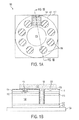
- FIG. 1A shows a top view of the TSV structure 100 , including a top pad 102 , an interconnect pad 104 and dummy structures 106 .
- the through silicon via structure 100 further includes a vertical conductive post 105 that is connected to the top pad 102 .
- the top pad 102 covers a wider area than the cross section of the vertical conductive post 105 .
- An interconnect pad 104 is located at least partially below the top pad 102 .
- An under layer 107 is also located at least partially below the top pad 102 .
- At least one dummy structure 106 connects the top pad 102 and the under layer 107 , fastening the top pad 102 and the interconnect pad 104 ,
- the dummy structures 106 are distributed circularly around the vertical conductive post 105 in one embodiment.
- FIG. 1B shows a cross section view of the TSV structure 100 along the cross section line 1 B according to one embodiment.
- the top pad 102 is connected to the vertical conductive post 105 to form a TSV.
- the interconnect pad 104 is also shown under the top pad 102 .
- the dummy structure 106 connects the top pad 102 and the under layer 107 (in FIG. 1A ).
- the under layer 107 can include a seed layer 118 , an isolation layer 116 , the second passivation layer 114 , any other suitable layer (e.g. dummy interconnect layer), or any combinations thereof.
- the vertical conductive post 105 is connected to a backside interconnect layer 120 through a substrate 108 .
- the backside interconnect layer 120 is shown on top of an electroless nickel/immersion gold (ENIG) layer 122 and the dicing tape 124 , On the substrate 108 , the first passivation layer 110 , the second passivation layers 112 and 114 are also shown.
- ENIG electroless nickel/immersion gold
- the dummy structures 106 fasten the top pad 102 and interconnect pad 104 to improve the reliability and interconnection performance.
- the dummy structures 106 increase the thermal tolerance of the structure and improve the adhesion between the top pad 102 and the interconnect pad 104 .
- the top pad 102 and the vertical conductive post 105 can comprise copper, tungsten, or any other suitable material.
- the top pad 102 can have a diameter about 15 ⁇ m-about 50 ⁇ m in some embodiments.
- the interconnect pad 104 can comprise Al, AlCu, Cu, or any other suitable material.
- the interconnect pad 104 can have a length/width about 5 ⁇ m-about 60 ⁇ m.
- the vertical conductive post 105 can have a depth about 50 ⁇ m-about 200 ⁇ m in some embodiments,
- the TSV structure 100 may have different geometries and dimensions for enhanced performance in various embodiments.
- the dummy structures 106 can also comprise copper, tungsten, or any other suitable material.
- the dummy structures 106 can have a diameter about 0.5 ⁇ m-about 10 ⁇ m and a depth about 0.5 ⁇ m-about 2 ⁇ m in some embodiments.
- the area ratio between the dummy structure 106 and the top pad 102 can be about 5%-about 40% in some embodiments.
- the interconnect pad 104 can have a length or a width about 5 ⁇ m-about 60 ⁇ m in some embodiments.
- the isolation layer 116 can comprise dielectric material, and have a thickness of about 0.5 ⁇ m-about 2 ⁇ m in some embodiments.
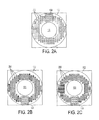
- FIG. 2A-FIG . 2 C are top views of a through silicon via (TSV) structure including one or more dummy structure according to some embodiments.
- dummy structures 202 have, for example, a circular shape, and they are distributed around the vertical conductive post 105 .
- the dummy structures 202 can be distributed uniformly under the top pad 102 except an area where the top pad 102 is connected to the vertical conductive post 105 .
- the dummy structures 202 can be distributed in a square grid pattern.
- the dummy structures 204 have a linear shape.
- the linear shape can be a straight line.
- the dummy structures 204 can be evenly spaced from each other.
- the dummy structures 204 can have at least two different lengths.
- the dummy structures 206 also have a linear shape and aligned in a different direction compared to FIG. 2B .
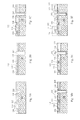
- FIG. 3A-FIG . 3 L are cross-sectional views of a through silicon via (TSV) structure including one or more dummy structure at various manufacturing stages.
- TSV through silicon via
- the process includes TSV etching to provide space for TSV, TSV isolation to prevent undesired contact, creating openings for TSV connection with interconnect pad, and TSV plating (e.g., Cu).
- the substrate 108 is a semiconductor wafer. in another example, the substrate 108 includes a semiconductor chip. In at least one embodiment, the substrate 108 includes silicon. In some other embodiments, the substrate 108 may alternatively or additionally include other elementary semiconductor, such as germanium. The substrate 108 may also include a compound semiconductor, such as silicon carbide, gallium arsenic, indium arsenide, and indium phosphide.
- the substrate 108 may include an epitaxial layer.
- the substrate 108 may have an epitaxial layer overlying a bulk semiconductor.
- the substrate 108 may be strained for performance enhancement.
- the epitaxial layer may include semiconductor materials different from those of the bulk semiconductor such as a layer of silicon germanium overlying bulk silicon, or a layer of silicon overlying a bulk silicon germanium formed by a process including selective epitaxial growth (SEG).
- the substrate 108 may include a semiconductor-on-insulator (SOI) structure.
- the substrate 108 includes a buried oxide (BOX) layer formed by a process such as separation by implanted oxygen (SIMOX).
- the substrate 108 can include various doped wells and other doped features configured and coupled to form various microelectronic devices such as metal-insulator-semiconductor field effect transistor (MOSFET) including complementary MOSFET (CMOS), imaging sensor including CMOS imaging sensor (CIS), micro-electro-mechanical system (MEMS), and/or other suitable active and/or passive devices,
- MOSFET metal-insulator-semiconductor field effect transistor
- CMOS complementary MOSFET
- imaging sensor including CMOS imaging sensor (CIS)
- MEMS micro-electro-mechanical system
- the doped wells and other doped features include p-type doped region and/or an n-type doped region, formed by a doping process such as ion implantation.
- the substrate 108 also includes various isolation features configured to separate various devices from each other for proper isolation.
- the isolation features may include different structures and can be formed by certain particular processing technologies.
- the isolation features include dielectric isolation such as shallow trench isolation (STI).
- the STI can be fabricated by etching the substrate to form a trench and filling the trench with a dielectric material.
- an interconnect structure can formed on the substrate 108 and configured to properly connect various doped regions in the substrate, resulting in the integrated circuit with designed functions.
- the interconnect structure can include multilayer interconnect (MLI) having horizontal conductive features (metal lines) disposed at multiple metal layers and vertical conductive features, such as contacts and vias.
- a via is configured to connect two metal lines at different metal layers.
- a contact is configured to connect a metal line and the substrate 108 .
- the multi layer interconnect may include conductive materials such as aluminum, aluminum/silicon/copper alloy, titanium, titanium nitride, tungsten, polysilicon, metal silicide, or combinations thereof.
- Aluminum interconnect can be formed by a process including physical vapor deposition (PVD such as PVD by sputtering), chemical vapor deposition (CVD), or combinations thereof.
- PVD physical vapor deposition
- CVD chemical vapor deposition
- Other manufacturing techniques to form the aluminum interconnect may include photolithography processing and etching to pattern the conductive materials for vertical (via and contact) and horizontal connects (conductive line).
- thermal annealing may be used to form metal silicide to reduce contact resistance.
- a copper or other interconnect may be used.
- Copper or other interconnect may include copper, copper alloy, titanium, titanium nitride, tantalum, tantalum nitride, tungsten, polysilicon, metal silicide, or combinations thereof.
- the copper or other interconnect may be formed by a technique such as CVD, sputtering, plating, and/or other suitable processes.
- the metal silicide used in multilayer interconnects may include nickel silicide, cobalt silicide, tungsten silicide, tantalum silicide, titanium silicide, platinum silicide, erbium silicide, palladium silicide, or combinations thereof.
- dielectric material features can be disposed on the substrate 108 to isolate various conductive elements.
- the dielectric material features include an interlayer dielectric (ILD) disposed between the substrate and the first metal layer.
- the dielectric material features also include inter-metal dielectric (IMD) disposed between adjacent metal layers.
- the dielectric material features include a dielectric material such as silicon oxide, silicon nitride, silicon oxynitride, or spin-on glass (SOG).
- the dielectric material in some alternative embodiments, includes a material of a low dielectric constant (low k) such as a dielectric constant less than about 3.5.
- the dielectric material may include silicon dioxide, silicon nitride, silicon oxynitride, spin-on glass (SOG), fluoride-doped silicate glass (FSG), carbon doped silicon oxide, BLACK DIAMOND® (Applied Materials of Santa Clara, Calif.), Xerogel, Aerogel, amorphous fluorinated carbon, Parylene, BCC (bis-benzocyclobutenes), SILK (Dow Chemical, Midland, Mich.), polyimide, and/or other suitable materials.
- the dielectric material features can be formed by a technique including spin-on coating, CVD, or other suitable processes.
- a first passivation layer 110 is formed on the substrate 108 and second passivation layers 112 and 114 are formed on the e first passivation layer 110 ,
- the first and second passivation layers each may include various passivation materials.
- the first passivation layer 110 includes silicon oxide.
- the silicon oxide passivation layer may have a thickness ranging between about 0.2 ⁇ m. and about 2 ⁇ m, in another example, the silicon oxide passivation layer may be formed by a high density plasma CVD process.
- the second passivation layers 112 and 114 comprise silicon nitride and/or silicon oxynitride.
- the second passivation layers 112 and 114 may have a thickness ranging between about 2 ⁇ m and about 6 ⁇ m.
- a silicon nitride passivation layer is formed by a plasma enhanced CVD (MOM) process.
- the precursors used to form silicon nitride in CVD include Hexachlorodisilane (Si 2 Cl 6 ), Dichlorosilane (SiH 2 Cl 2 ), Bis(TertiaryButylAmino)Silane (C 8 H 22 N 2 Si), and/or Disilane (Si 2 H 6 ).
- the interconnect pads 104 are also formed over the substrate 108 .
- the interconnect pads 104 can have a thickness about 1 ⁇ m-about 4 ⁇ m in some embodiments.
- the interconnect pads 104 are disposed on the first passivation layer 110 and positioned at least partially within the openings of the second passivation layers 112 and 114 .
- the interconnect pads 104 include aluminum.
- an aluminum layer is deposited on the first passivation layer 110 and within the openings of the second passivation layers 112 and 114 to connect to interconnect structures.
- the aluminum layer is then patterned to form the various interconnect pads 104 .
- the second passivation layer 112 and 114 are deposited on the first passivation layer 110 .
- the second passivation layer 114 deposited on the interconnect pads 104 is then patterned to expose the interconnect pads 104 .
- Interconnect pads 104 can include conductive materials such as aluminum, aluminum/silicon/copper alloy, titanium, titanium nitride, tungsten, polysilicon, metal silicide, or combinations thereof.
- Aluminum interconnect pads can be formed by a process including physical vapor deposition (PVD such as PVD by sputtering), chemical vapor deposition (CVD), or combinations thereof.
- PVD physical vapor deposition
- CVD chemical vapor deposition
- Other manufacturing techniques to form the aluminum interconnect pad may include photolithography processing and etching to pattern the conductive materials for vertical (via and contact) and horizontal connects (conductive line). Still other manufacturing processes such as thermal annealing may be used to form metal silicide to reduce contact resistance.
- a copper or other interconnect pad may be used.
- Copper or other interconnect pad may include copper, copper alloy, titanium, titanium nitride, tantalum, tantalum nitride, tungsten, polysilicon, metal silicide, or combinations.
- the copper or other interconnect may be formed by a technique such as CVD, sputtering, plating, or other suitable processes.
- the metal suicide used in multilayer interconnects may include nickel silicide, cobalt suicide, tungsten silicide, tantalum silicide, titanium silicide, platinum silicide, erbium silicide, palladium silicide, or combinations thereof.
- TSV etching such as a dry plasma etching process is performed to form the TSV opening 302 through the first passivation layer 110 , the second passivation layers 112 and 114 .
- Plasma etch can be performed in several modes by adjusting the parameters of the plasma. Ordinary plasma etching operates between 0.1 and 5 torr. The plasma produces energetic free radicals, neutrally charged, that react at the surface of the wafer. Since neutral particles attack the wafer from all angles, this process is isotropic.
- the source gas for the plasma usually contains small molecules rich in chlorine or fluorine. For instance, in some embodiments, carbon tetrachloride (CC14) can be used to etch silicon and aluminum, and trifluoromethane can be used to etch silicon dioxide and silicon nitride.
- additional TSV etching such as a dry plasma etching process is performed to form a deeper TSV opening 302 partially through the substrate 108 .
- the TSV opening 302 does not extend all the way through the substrate 108 , but the rest of the substrate 108 can be removed later. For example, backside polishing at a later stage can be performed.
- the isolation layer 116 is deposited over the interconnect pads 104 and the second passivation layer 114 .
- the isolation layer 116 may comprise silicon oxide layer, tetraethoxysilane (TEOS), silica glass, or any other suitable material.
- TEOS tetraethoxysilane
- the isolation layer 116 may have a thickness about 0.5 ⁇ m-about 2 ⁇ m in one embodiment.
- photo resist (PR) layer 304 can be deposited by spray coating or spin coating, and then openings 303 for dummy structures are etched out.
- the thickness of PR layer 304 can be about 1 ⁇ m-about 5 ⁇ m.
- spin coating is used to form thin films with uniform thickness over flat substrates. An excess amount of a solution is placed on the substrate, which is then rotated at high speed in order to spread the fluid by centrifugal force. Rotation is continued while the fluid spins off the edges of the substrate, until the desired thickness of the film is achieved. Photoresist is typically spun at 20 to 80 revolutions per second for 30 to 60 seconds.
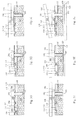
- PR layer 304 is removed and seed layer 118 is deposited.
- the seed layer 118 can comprise Cu, Ti, TiN, W, any other suitable material, or any combinations thereof in some embodiments.
- a copper seed layer can be formed by physical vapor deposition (PVD) such as PVD by sputtering.
- the seed layer 118 can have a thickness ranging between about 10 nm and about 600 nm.
- the PR layer 306 can be either liquid PR or dry film PR.
- the PR layer 306 prevents metal deposit in undesired areas in the next stage.
- a TSV including top pad 102 and vertical conductive post 105 is formed as well as dummy structures 106 over the seed layer 118 by a suitable method such as plating a metal layer (e.g. copper, tungsten, any other suitable material). Other process may be further followed. For example, a chemical mechanic polishing (CMP) process may he applied thereafter to planarize the surface.
- CMP chemical mechanic polishing
- the metal layer may be further patterned to form the TSV. For example, if a copper layer is implemented, then a damascene process can be used to form patterned copper features including TSV.
- the top pad 102 of the TSV is connected to one of the interconnect pads 104 .
- wafers and/or chips can be stacked vertically and coupled through TSV features.
- TSV 3D package creates vertical connections through chip body and eliminates additional wire.
- the top pad 102 may have a diameter about 15 ⁇ m-50 ⁇ m and the vertical conductive post 105 may have a depth about 50 ⁇ m-200 ⁇ m in embodiments.
- the top pad 102 and the vertical conductive post 105 of the TSV may have different geometries and dimensions for enhanced performance in various embodiments.
- the PR film 306 is removed and seed layer 118 outside the top pad 102 area is etched out.
- a liquid resist stripper can be used, which chemically alters the resist so that it no longer adheres to the layer below.
- photoresist may be removed by ashing, i.e. a plasma containing oxygen that oxidizes the photoresist.
- a carrier 308 is placed over the substrate 108 so that the backside processing of the substrate 108 can be performed.
- the backside of the substrate 108 is ground and polished.
- the backside polishing process thins the substrate 108 and exposes the vertical conductive post 105 of the TSV from the backside of the substrate 108 for 3-D packaging,
- the TSV can be coupled to other wafer/chip in embodiments.
- interconnect layer 120 and electroless nickel/immersion gold (ENIG) layer 122 can be formed.
- aluminum sputtering can be performed to form the interconnect layer 120 with a thickness of about 1 ⁇ m to about 5 ⁇ m.
- the ENIG layer 122 can have a thickness of about 100 nm-about 4 ⁇ m.
- the carrier 308 is debonded and dicing tape 124 is put on under the substrate 108 .
- the dicing tape 124 can comprise a polymer tape.
- the dicing tape 124 has a sticky backing that holds the wafer on a thin sheet metal frame. Once a wafer has been diced, the remaining components that are left on the dicing tape 124 are referred to as die, dice or dies. The die will stay on the dicing tape 124 until they are extracted by die handling equipment, like a die bonder or die sorter, further in the electronics assembly process.
- the TSV structure 100 disclosed herein can improve its temperature tolerance. For example, a conventional structure contact resistance shifted significantly within one day under one stress test. In comparison, the TSV structure 100 using one or more dummy structure 106 as described above can keep the same performance more than 2000 hrs under the same stress test. A skilled person in the art will appreciate that there can be many embodiment variations of this invention.
Abstract
Description
- The present application is a divisional application of U.S. patent application Ser. No. 12/791,978, filed on Jun. 2, 2010, which claims priority of U.S. Provisional Patent Application Ser. No. 61/254,043, filed on Oct. 22, 2009, the entire disclosures of which are incorporated herein by reference.
- The present disclosure relates generally to the field of semiconductor circuits, and more particularly, to a through-silicon-via. (TSV) structure for integrated circuits.
- A through-silicon via (TSV) is a vertical electrical connection passing through a silicon wafer or die. TSV technology is important in creating 3-dimensional (3D) packages and 3D integrated circuits. A 3D package, e.g. system in package, chip stack multi-chip module (MCM), etc., contains two or more chips (integrated circuits) stacked vertically so that they occupy less space.
- In most 3D packages, the stacked chips arc wired together along their edges; this edge wiring slightly increases the length and width of the package and usually requires an extra interposer layer between the chips. In some new 3D packages, through-silicon vias replace edge wiring by creating vertical connections through the body of the chips. The resulting package has no added length or width. Because no interposer is required, a TSV 3D package can also be flatter than an edge-wired 3D package.
- A 3D integrated circuit is a single integrated circuit built by stacking silicon wafers and/or dies and interconnecting them vertically so that they are packaged as a single device. By using TSV technology, 3D ICs can pack a great deal of functionality into a small footprint. In addition, critical electrical paths through the device can be drastically shortened, leading to faster operation.
- However, interface failure between TSV and interconnect pad is problematic. For example, copper TSV connected to an aluminum interconnect pad suffers high thermal stress because of temperature coefficient difference and the large thickness of copper. The failure location is typically at an interface between Cu and Al/AlCu, The cause of the failure is Cu delamination induced by Joule heating or higher temperature.
- For a more complete understanding of the present disclosure, and the advantages thereof, reference is now made to the following descriptions taken in conjunction with the accompanying drawings, in which:
-
FIG. 1A-FIG . 1B are a top view and a cross-sectional view of a through silicon via (TSV) structure including one or more dummy structure according to sonic embodiments; -
FIG. 2A-FIG . 2C are top views of a through silicon via (TSV) structure including one or more dummy structure according to some embodiments; and -
FIG. 3A-FIG . 3L are cross-sectional views of a through silicon via (TSV) structure including one or more dummy structure at various manufacturing stages. - The making and using of various embodiments are discussed in detail below. It should he appreciated, however, that the present disclosure provides many applicable inventive concepts that can be embodied in a wide variety of specific contexts. The specific embodiments discussed are merely illustrative of specific ways to make and use, and do not limit the scope of the invention.
- A structure of through silicon via (TSV) using one or more dummy structure to improve adhesion to the interconnect pad and a method to fabricate the same are provided.
FIG. 1A-FIG . 1B are a top view and a cross-sectional view of a through silicon via (TSV) structure including one or more dummy structure according to some embodiments.FIG. 1A shows a top view of the TSVstructure 100, including atop pad 102, aninterconnect pad 104 anddummy structures 106. The through silicon viastructure 100 further includes a verticalconductive post 105 that is connected to thetop pad 102. Thetop pad 102 covers a wider area than the cross section of the verticalconductive post 105. Aninterconnect pad 104 is located at least partially below thetop pad 102. An underlayer 107 is also located at least partially below thetop pad 102. At least onedummy structure 106 connects thetop pad 102 and the underlayer 107, fastening thetop pad 102 and theinterconnect pad 104, Thedummy structures 106 are distributed circularly around the verticalconductive post 105 in one embodiment. -
FIG. 1B shows a cross section view of theTSV structure 100 along the cross section line 1B according to one embodiment. Thetop pad 102 is connected to the verticalconductive post 105 to form a TSV. Theinterconnect pad 104 is also shown under thetop pad 102. Thedummy structure 106 connects thetop pad 102 and the under layer 107 (inFIG. 1A ). Depending on implementations, in some embodiments, the underlayer 107 can include aseed layer 118, anisolation layer 116, thesecond passivation layer 114, any other suitable layer (e.g. dummy interconnect layer), or any combinations thereof. - The vertical
conductive post 105 is connected to abackside interconnect layer 120 through asubstrate 108. Thebackside interconnect layer 120 is shown on top of an electroless nickel/immersion gold (ENIG)layer 122 and thedicing tape 124, On thesubstrate 108, thefirst passivation layer 110, thesecond passivation layers - The
dummy structures 106 fasten thetop pad 102 andinterconnect pad 104 to improve the reliability and interconnection performance. Thedummy structures 106 increase the thermal tolerance of the structure and improve the adhesion between thetop pad 102 and theinterconnect pad 104. Thetop pad 102 and the verticalconductive post 105 can comprise copper, tungsten, or any other suitable material. Thetop pad 102 can have a diameter about 15 μm-about 50 μm in some embodiments. Theinterconnect pad 104 can comprise Al, AlCu, Cu, or any other suitable material. Theinterconnect pad 104 can have a length/width about 5 μm-about 60 μm. The verticalconductive post 105 can have a depth about 50 μm-about 200 μm in some embodiments, The TSVstructure 100 may have different geometries and dimensions for enhanced performance in various embodiments. - The
dummy structures 106 can also comprise copper, tungsten, or any other suitable material. Thedummy structures 106 can have a diameter about 0.5 μm-about 10 μm and a depth about 0.5 μm-about 2 μm in some embodiments. The area ratio between thedummy structure 106 and thetop pad 102 can be about 5%-about 40% in some embodiments. Theinterconnect pad 104 can have a length or a width about 5 μm-about 60 μm in some embodiments. Theisolation layer 116 can comprise dielectric material, and have a thickness of about 0.5 μm-about 2 μm in some embodiments. -
FIG. 2A-FIG . 2C are top views of a through silicon via (TSV) structure including one or more dummy structure according to some embodiments. InFIG. 2A ,dummy structures 202 have, for example, a circular shape, and they are distributed around the verticalconductive post 105. Thedummy structures 202 can be distributed uniformly under thetop pad 102 except an area where thetop pad 102 is connected to the verticalconductive post 105. Thedummy structures 202 can be distributed in a square grid pattern. InFIG. 2B , thedummy structures 204 have a linear shape. The linear shape can be a straight line. Thedummy structures 204 can be evenly spaced from each other. Thedummy structures 204 can have at least two different lengths. InFIG. 2C , thedummy structures 206 also have a linear shape and aligned in a different direction compared toFIG. 2B . -
FIG. 3A-FIG . 3L are cross-sectional views of a through silicon via (TSV) structure including one or more dummy structure at various manufacturing stages. In general, the process includes TSV etching to provide space for TSV, TSV isolation to prevent undesired contact, creating openings for TSV connection with interconnect pad, and TSV plating (e.g., Cu). - Referring to
FIG. 3A , asubstrate 108 is shown. In one example, thesubstrate 108 is a semiconductor wafer. in another example, thesubstrate 108 includes a semiconductor chip. In at least one embodiment, thesubstrate 108 includes silicon. In some other embodiments, thesubstrate 108 may alternatively or additionally include other elementary semiconductor, such as germanium. Thesubstrate 108 may also include a compound semiconductor, such as silicon carbide, gallium arsenic, indium arsenide, and indium phosphide. - The
substrate 108 may include an epitaxial layer. For example, thesubstrate 108 may have an epitaxial layer overlying a bulk semiconductor. Further, thesubstrate 108 may be strained for performance enhancement. For example, the epitaxial layer may include semiconductor materials different from those of the bulk semiconductor such as a layer of silicon germanium overlying bulk silicon, or a layer of silicon overlying a bulk silicon germanium formed by a process including selective epitaxial growth (SEG). Furthermore, thesubstrate 108 may include a semiconductor-on-insulator (SOI) structure. In various examples, thesubstrate 108 includes a buried oxide (BOX) layer formed by a process such as separation by implanted oxygen (SIMOX). - In some embodiments, the
substrate 108 can include various doped wells and other doped features configured and coupled to form various microelectronic devices such as metal-insulator-semiconductor field effect transistor (MOSFET) including complementary MOSFET (CMOS), imaging sensor including CMOS imaging sensor (CIS), micro-electro-mechanical system (MEMS), and/or other suitable active and/or passive devices, The doped wells and other doped features include p-type doped region and/or an n-type doped region, formed by a doping process such as ion implantation. - Other structures such as gate dielectric and polysilicon gate electrodes may be additionally formed on the
substrate 108 for devices such as MOSFET devices. Thesubstrate 108 also includes various isolation features configured to separate various devices from each other for proper isolation. The isolation features may include different structures and can be formed by certain particular processing technologies. In one example, the isolation features include dielectric isolation such as shallow trench isolation (STI). The STI can be fabricated by etching the substrate to form a trench and filling the trench with a dielectric material. - Also, an interconnect structure can formed on the
substrate 108 and configured to properly connect various doped regions in the substrate, resulting in the integrated circuit with designed functions. The interconnect structure can include multilayer interconnect (MLI) having horizontal conductive features (metal lines) disposed at multiple metal layers and vertical conductive features, such as contacts and vias. A via is configured to connect two metal lines at different metal layers. A contact is configured to connect a metal line and thesubstrate 108. The multi layer interconnect may include conductive materials such as aluminum, aluminum/silicon/copper alloy, titanium, titanium nitride, tungsten, polysilicon, metal silicide, or combinations thereof. - Aluminum interconnect can be formed by a process including physical vapor deposition (PVD such as PVD by sputtering), chemical vapor deposition (CVD), or combinations thereof. Other manufacturing techniques to form the aluminum interconnect may include photolithography processing and etching to pattern the conductive materials for vertical (via and contact) and horizontal connects (conductive line). In some embodiments, still other manufacturing processes such as thermal annealing may be used to form metal silicide to reduce contact resistance.
- In some alternative embodiments, a copper or other interconnect may be used. Copper or other interconnect may include copper, copper alloy, titanium, titanium nitride, tantalum, tantalum nitride, tungsten, polysilicon, metal silicide, or combinations thereof. The copper or other interconnect may be formed by a technique such as CVD, sputtering, plating, and/or other suitable processes. The metal silicide used in multilayer interconnects may include nickel silicide, cobalt silicide, tungsten silicide, tantalum silicide, titanium silicide, platinum silicide, erbium silicide, palladium silicide, or combinations thereof.
- In addition, dielectric material features can be disposed on the
substrate 108 to isolate various conductive elements. The dielectric material features include an interlayer dielectric (ILD) disposed between the substrate and the first metal layer. The dielectric material features also include inter-metal dielectric (IMD) disposed between adjacent metal layers. The dielectric material features include a dielectric material such as silicon oxide, silicon nitride, silicon oxynitride, or spin-on glass (SOG). The dielectric material, in some alternative embodiments, includes a material of a low dielectric constant (low k) such as a dielectric constant less than about 3.5. in various examples, the dielectric material may include silicon dioxide, silicon nitride, silicon oxynitride, spin-on glass (SOG), fluoride-doped silicate glass (FSG), carbon doped silicon oxide, BLACK DIAMOND® (Applied Materials of Santa Clara, Calif.), Xerogel, Aerogel, amorphous fluorinated carbon, Parylene, BCC (bis-benzocyclobutenes), SILK (Dow Chemical, Midland, Mich.), polyimide, and/or other suitable materials. The dielectric material features can be formed by a technique including spin-on coating, CVD, or other suitable processes. - In
FIG. 3A , afirst passivation layer 110 is formed on thesubstrate 108 and second passivation layers 112 and 114 are formed on the efirst passivation layer 110, The first and second passivation layers each may include various passivation materials. In one embodiment, thefirst passivation layer 110 includes silicon oxide. In one example, the silicon oxide passivation layer may have a thickness ranging between about 0.2 μm. and about 2 μm, in another example, the silicon oxide passivation layer may be formed by a high density plasma CVD process. In another embodiment, the second passivation layers 112 and 114 comprise silicon nitride and/or silicon oxynitride. In one example, the second passivation layers 112 and 114 may have a thickness ranging between about 2 μm and about 6 μm. In one example, a silicon nitride passivation layer is formed by a plasma enhanced CVD (MOM) process. The precursors used to form silicon nitride in CVD include Hexachlorodisilane (Si2Cl6), Dichlorosilane (SiH2Cl2), Bis(TertiaryButylAmino)Silane (C8H22N2Si), and/or Disilane (Si2H6). - The
interconnect pads 104 are also formed over thesubstrate 108. Theinterconnect pads 104 can have a thickness about 1 μm-about 4 μm in some embodiments. Theinterconnect pads 104 are disposed on thefirst passivation layer 110 and positioned at least partially within the openings of the second passivation layers 112 and 114. In one example, theinterconnect pads 104 include aluminum. In one embodiment of the interconnect pad formation, an aluminum layer is deposited on thefirst passivation layer 110 and within the openings of the second passivation layers 112 and 114 to connect to interconnect structures. The aluminum layer is then patterned to form thevarious interconnect pads 104. Thesecond passivation layer first passivation layer 110. Thesecond passivation layer 114 deposited on theinterconnect pads 104 is then patterned to expose theinterconnect pads 104. -
Interconnect pads 104 can include conductive materials such as aluminum, aluminum/silicon/copper alloy, titanium, titanium nitride, tungsten, polysilicon, metal silicide, or combinations thereof. Aluminum interconnect pads can be formed by a process including physical vapor deposition (PVD such as PVD by sputtering), chemical vapor deposition (CVD), or combinations thereof. Other manufacturing techniques to form the aluminum interconnect pad may include photolithography processing and etching to pattern the conductive materials for vertical (via and contact) and horizontal connects (conductive line). Still other manufacturing processes such as thermal annealing may be used to form metal silicide to reduce contact resistance. In some alternative embodiments, a copper or other interconnect pad may be used. Copper or other interconnect pad may include copper, copper alloy, titanium, titanium nitride, tantalum, tantalum nitride, tungsten, polysilicon, metal silicide, or combinations. The copper or other interconnect may be formed by a technique such as CVD, sputtering, plating, or other suitable processes. The metal suicide used in multilayer interconnects may include nickel silicide, cobalt suicide, tungsten silicide, tantalum silicide, titanium silicide, platinum silicide, erbium silicide, palladium silicide, or combinations thereof. - In
FIG. 3A , TSV etching such as a dry plasma etching process is performed to form theTSV opening 302 through thefirst passivation layer 110, the second passivation layers 112 and 114. Plasma etch can be performed in several modes by adjusting the parameters of the plasma. Ordinary plasma etching operates between 0.1 and 5 torr. The plasma produces energetic free radicals, neutrally charged, that react at the surface of the wafer. Since neutral particles attack the wafer from all angles, this process is isotropic. The source gas for the plasma usually contains small molecules rich in chlorine or fluorine. For instance, in some embodiments, carbon tetrachloride (CC14) can be used to etch silicon and aluminum, and trifluoromethane can be used to etch silicon dioxide and silicon nitride. - In
FIG. 3B , additional TSV etching such as a dry plasma etching process is performed to form adeeper TSV opening 302 partially through thesubstrate 108. In some embodiments, theTSV opening 302 does not extend all the way through thesubstrate 108, but the rest of thesubstrate 108 can be removed later. For example, backside polishing at a later stage can be performed. - In
FIG. 3C , theisolation layer 116 is deposited over theinterconnect pads 104 and thesecond passivation layer 114. Theisolation layer 116 may comprise silicon oxide layer, tetraethoxysilane (TEOS), silica glass, or any other suitable material. Theisolation layer 116 may have a thickness about 0.5 μm-about 2 μm in one embodiment. - In
FIG. 3D , photo resist (PR)layer 304 can be deposited by spray coating or spin coating, and thenopenings 303 for dummy structures are etched out. In one embodiment, the thickness ofPR layer 304 can be about 1 μm-about 5 μm. In one example, spin coating is used to form thin films with uniform thickness over flat substrates. An excess amount of a solution is placed on the substrate, which is then rotated at high speed in order to spread the fluid by centrifugal force. Rotation is continued while the fluid spins off the edges of the substrate, until the desired thickness of the film is achieved. Photoresist is typically spun at 20 to 80 revolutions per second for 30 to 60 seconds. - In
FIG. 3E ,PR layer 304 is removed andseed layer 118 is deposited. Theseed layer 118 can comprise Cu, Ti, TiN, W, any other suitable material, or any combinations thereof in some embodiments. In one example, a copper seed layer can be formed by physical vapor deposition (PVD) such as PVD by sputtering. In one embodiment, theseed layer 118 can have a thickness ranging between about 10 nm and about 600 nm. - In
FIG. 3F , anotherPR layer 306 is formed. ThePR layer 306 can be either liquid PR or dry film PR. ThePR layer 306 prevents metal deposit in undesired areas in the next stage. - In
FIG. 3G , a TSV includingtop pad 102 and verticalconductive post 105 is formed as well asdummy structures 106 over theseed layer 118 by a suitable method such as plating a metal layer (e.g. copper, tungsten, any other suitable material). Other process may be further followed. For example, a chemical mechanic polishing (CMP) process may he applied thereafter to planarize the surface. The metal layer may be further patterned to form the TSV. For example, if a copper layer is implemented, then a damascene process can be used to form patterned copper features including TSV. In one embodiment, thetop pad 102 of the TSV is connected to one of theinterconnect pads 104. In some embodiments, wafers and/or chips can be stacked vertically and coupled through TSV features. Such TSV 3D package creates vertical connections through chip body and eliminates additional wire. Thetop pad 102 may have a diameter about 15 μm-50 μm and the verticalconductive post 105 may have a depth about 50 μm-200 μm in embodiments. Thetop pad 102 and the verticalconductive post 105 of the TSV may have different geometries and dimensions for enhanced performance in various embodiments. - In
FIG. 3H , thePR film 306 is removed andseed layer 118 outside thetop pad 102 area is etched out. In one embodiment, a liquid resist stripper can be used, which chemically alters the resist so that it no longer adheres to the layer below. In some alternative embodiments, photoresist may be removed by ashing, i.e. a plasma containing oxygen that oxidizes the photoresist. - In
FIG. 3I , acarrier 308 is placed over thesubstrate 108 so that the backside processing of thesubstrate 108 can be performed. - In
FIG. 3J , the backside of thesubstrate 108 is ground and polished. The backside polishing process thins thesubstrate 108 and exposes the verticalconductive post 105 of the TSV from the backside of thesubstrate 108 for 3-D packaging, For example, the TSV can be coupled to other wafer/chip in embodiments. - In
FIG. 3K ,interconnect layer 120 and electroless nickel/immersion gold (ENIG)layer 122 can be formed. In one example, aluminum sputtering can be performed to form theinterconnect layer 120 with a thickness of about 1 μm to about 5 μm. TheENIG layer 122 can have a thickness of about 100 nm-about 4 μm. - In
FIG. 3L , thecarrier 308 is debonded and dicingtape 124 is put on under thesubstrate 108. In one example, the dicingtape 124 can comprise a polymer tape. The dicingtape 124 has a sticky backing that holds the wafer on a thin sheet metal frame. Once a wafer has been diced, the remaining components that are left on the dicingtape 124 are referred to as die, dice or dies. The die will stay on the dicingtape 124 until they are extracted by die handling equipment, like a die bonder or die sorter, further in the electronics assembly process. - The
TSV structure 100 disclosed herein can improve its temperature tolerance. For example, a conventional structure contact resistance shifted significantly within one day under one stress test. In comparison, theTSV structure 100 using one ormore dummy structure 106 as described above can keep the same performance more than 2000 hrs under the same stress test. A skilled person in the art will appreciate that there can be many embodiment variations of this invention. - Although exemplary embodiments of the present invention and their advantages have been described in detail, it should be understood that various changes, substitutions and alterations can be made herein without departing from the spirit and scope of the invention as defined by the appended claims, Moreover, the scope of the present application is not intended to be limited to the particular embodiments of the process, machine, manufacture, and composition of matter, means, methods and steps described in the specification. As one of ordinary skill in the art will readily appreciate from the disclosure herein, processes, machines, manufacture, compositions of matter, means, methods, or steps, presently existing or later to be developed, that perform substantially the same function or achieve substantially the same result as the corresponding embodiments described herein may be utilized according to the present invention. Accordingly, the appended claims are intended to include within their scope such processes, machines, manufacture, compositions of matter, means, methods, or steps.
Claims (20)
Priority Applications (1)
| Application Number | Priority Date | Filing Date | Title |
|---|---|---|---|
| US13/112,347 US8202800B2 (en) | 2009-10-22 | 2011-05-20 | Method of forming through silicon via with dummy structure |
Applications Claiming Priority (3)
| Application Number | Priority Date | Filing Date | Title |
|---|---|---|---|
| US25404309P | 2009-10-22 | 2009-10-22 | |
| US12/791,978 US7969013B2 (en) | 2009-10-22 | 2010-06-02 | Through silicon via with dummy structure and method for forming the same |
| US13/112,347 US8202800B2 (en) | 2009-10-22 | 2011-05-20 | Method of forming through silicon via with dummy structure |
Related Parent Applications (1)
| Application Number | Title | Priority Date | Filing Date |
|---|---|---|---|
| US12/791,978 Division US7969013B2 (en) | 2009-10-22 | 2010-06-02 | Through silicon via with dummy structure and method for forming the same |
Publications (2)
| Publication Number | Publication Date |
|---|---|
| US20110217841A1 true US20110217841A1 (en) | 2011-09-08 |
| US8202800B2 US8202800B2 (en) | 2012-06-19 |
Family
ID=43897696
Family Applications (2)
| Application Number | Title | Priority Date | Filing Date |
|---|---|---|---|
| US12/791,978 Active US7969013B2 (en) | 2009-10-22 | 2010-06-02 | Through silicon via with dummy structure and method for forming the same |
| US13/112,347 Active US8202800B2 (en) | 2009-10-22 | 2011-05-20 | Method of forming through silicon via with dummy structure |
Family Applications Before (1)
| Application Number | Title | Priority Date | Filing Date |
|---|---|---|---|
| US12/791,978 Active US7969013B2 (en) | 2009-10-22 | 2010-06-02 | Through silicon via with dummy structure and method for forming the same |
Country Status (2)
| Country | Link |
|---|---|
| US (2) | US7969013B2 (en) |
| CN (1) | CN102074544B (en) |
Cited By (10)
| Publication number | Priority date | Publication date | Assignee | Title |
|---|---|---|---|---|
| US20130140688A1 (en) * | 2011-12-02 | 2013-06-06 | Chun-Hung Chen | Through Silicon Via and Method of Manufacturing the Same |
| US20140021562A1 (en) * | 2012-07-23 | 2014-01-23 | Seiko Epson Corporation | Mems device, electronic module, electronic apparatus, and mobile unit |
| US8900969B2 (en) | 2012-01-27 | 2014-12-02 | Skyworks Solutions, Inc. | Methods of stress balancing in gallium arsenide wafer processing |
| US9070748B2 (en) | 2012-12-20 | 2015-06-30 | Samsung Electronics Co., Ltd. | Semiconductor devices having through-vias and methods for fabricating the same |
| US9093506B2 (en) | 2012-05-08 | 2015-07-28 | Skyworks Solutions, Inc. | Process for fabricating gallium arsenide devices with copper contact layer |
| US20150371936A1 (en) * | 2014-06-18 | 2015-12-24 | Taiwan Semiconductor Manufacturing Company, Ltd. | Semiconductor Device Packages, Packaging Methods, and Packaged Semiconductor Devices |
| US20150371947A1 (en) * | 2014-06-18 | 2015-12-24 | Taiwan Semiconductor Manufacturing Company, Ltd. | Devices, Packaging Devices, and Methods of Packaging Semiconductor Devices |
| US9425126B2 (en) * | 2014-05-29 | 2016-08-23 | Taiwan Semiconductor Manufacturing Company, Ltd. | Dummy structure for chip-on-wafer-on-substrate |
| US9530719B2 (en) | 2014-06-13 | 2016-12-27 | Skyworks Solutions, Inc. | Direct die solder of gallium arsenide integrated circuit dies and methods of manufacturing gallium arsenide wafers |
| TWI790209B (en) * | 2016-09-30 | 2023-01-21 | 美商英特爾股份有限公司 | Finfet transistor with channel stress induced via stressor material inserted into fin plug region enabled by backside reveal |
Families Citing this family (42)
| Publication number | Priority date | Publication date | Assignee | Title |
|---|---|---|---|---|
| JP2011258687A (en) * | 2010-06-08 | 2011-12-22 | Renesas Electronics Corp | Semiconductor device and method of manufacturing the same |
| US8560982B2 (en) * | 2011-06-27 | 2013-10-15 | Xilinx, Inc. | Integrated circuit design using through silicon vias |
| US8618647B2 (en) * | 2011-08-01 | 2013-12-31 | Tessera, Inc. | Packaged microelectronic elements having blind vias for heat dissipation |
| KR101840447B1 (en) * | 2011-08-09 | 2018-03-20 | 에스케이하이닉스 주식회사 | Semiconductor package and stacked semiconductor package having the same |
| US8546886B2 (en) | 2011-08-24 | 2013-10-01 | Taiwan Semiconductor Manufacturing Company, Ltd. | Controlling the device performance by forming a stressed backside dielectric layer |
| KR20130130524A (en) * | 2012-05-22 | 2013-12-02 | 삼성전자주식회사 | Semiconductor devices having a via pad |
| US10052705B2 (en) | 2012-08-30 | 2018-08-21 | Universal Instruments Corporation | 3D TSV assembly method for mass reflow |
| US8912844B2 (en) | 2012-10-09 | 2014-12-16 | United Microelectronics Corp. | Semiconductor structure and method for reducing noise therein |
| US9035457B2 (en) | 2012-11-29 | 2015-05-19 | United Microelectronics Corp. | Substrate with integrated passive devices and method of manufacturing the same |
| US8716104B1 (en) | 2012-12-20 | 2014-05-06 | United Microelectronics Corp. | Method of fabricating isolation structure |
| US9520811B2 (en) * | 2013-02-27 | 2016-12-13 | Texas Instruments Incorporated | Capacitive micromachined ultrasonic transducer (CMUT) device with through-substrate via (TSV) |
| US8957504B2 (en) * | 2013-03-15 | 2015-02-17 | IP Enval Consultant Inc. | Integrated structure with a silicon-through via |
| US8884398B2 (en) | 2013-04-01 | 2014-11-11 | United Microelectronics Corp. | Anti-fuse structure and programming method thereof |
| US9287173B2 (en) | 2013-05-23 | 2016-03-15 | United Microelectronics Corp. | Through silicon via and process thereof |
| US9123730B2 (en) | 2013-07-11 | 2015-09-01 | United Microelectronics Corp. | Semiconductor device having through silicon trench shielding structure surrounding RF circuit |
| US9024416B2 (en) | 2013-08-12 | 2015-05-05 | United Microelectronics Corp. | Semiconductor structure |
| US8916471B1 (en) | 2013-08-26 | 2014-12-23 | United Microelectronics Corp. | Method for forming semiconductor structure having through silicon via for signal and shielding structure |
| US9048223B2 (en) | 2013-09-03 | 2015-06-02 | United Microelectronics Corp. | Package structure having silicon through vias connected to ground potential |
| US9117804B2 (en) | 2013-09-13 | 2015-08-25 | United Microelectronics Corporation | Interposer structure and manufacturing method thereof |
| KR102142366B1 (en) | 2013-11-14 | 2020-08-07 | 삼성전자 주식회사 | Semiconductor intergrated circuit device, method for fabricating the same, and semiconductort pachage |
| US9343359B2 (en) | 2013-12-25 | 2016-05-17 | United Microelectronics Corp. | Integrated structure and method for fabricating the same |
| US10340203B2 (en) | 2014-02-07 | 2019-07-02 | United Microelectronics Corp. | Semiconductor structure with through silicon via and method for fabricating and testing the same |
| US9269607B2 (en) | 2014-06-17 | 2016-02-23 | Globalfoundries Inc. | Wafer stress control with backside patterning |
| KR102320821B1 (en) | 2014-09-11 | 2021-11-02 | 삼성전자주식회사 | Semiconductor package |
| US9818622B2 (en) | 2015-01-29 | 2017-11-14 | Micron Technology, Inc. | Uniform back side exposure of through-silicon vias |
| CN104576434A (en) * | 2015-02-02 | 2015-04-29 | 华进半导体封装先导技术研发中心有限公司 | Method for testing through holes in silicon |
| US9397048B1 (en) * | 2015-03-23 | 2016-07-19 | Inotera Memories, Inc. | Semiconductor structure and manufacturing method thereof |
| US9941190B2 (en) * | 2015-04-03 | 2018-04-10 | Micron Technology, Inc. | Semiconductor device having through-silicon-via and methods of forming the same |
| CN104952756A (en) * | 2015-06-12 | 2015-09-30 | 上海华岭集成电路技术股份有限公司 | Test device and test system for three-dimensional packaging base plate |
| KR20170011366A (en) * | 2015-07-22 | 2017-02-02 | 삼성전자주식회사 | Semiconductor chip and semiconductor package having the same |
| KR20170023643A (en) | 2015-08-24 | 2017-03-06 | 삼성전자주식회사 | Semiconductor device and method of manufacturing the same |
| CN106556790B (en) * | 2015-09-24 | 2020-05-12 | 中芯国际集成电路制造(上海)有限公司 | Through silicon via sensor, detection method and electronic device |
| US10867834B2 (en) * | 2015-12-31 | 2020-12-15 | Taiwan Semiconductor Manufacturing Company Ltd. | Semiconductor structure and manufacturing method thereof |
| JP6674016B2 (en) * | 2016-03-24 | 2020-04-01 | 京セラ株式会社 | Printed wiring board and manufacturing method thereof |
| JP7322011B2 (en) | 2017-11-02 | 2023-08-07 | ユニヴァーサル インストゥルメンツ コーポレイション | Cross-reference to related applications for fixtures and methods to hold components before and after reflow |
| CN108615704B (en) * | 2018-03-27 | 2020-05-08 | 中国科学院上海微系统与信息技术研究所 | Manufacturing process of through silicon via interconnection, through silicon via interconnection structure formed by manufacturing process and application of through silicon via interconnection structure |
| US10643957B2 (en) | 2018-08-27 | 2020-05-05 | Nxp B.V. | Conformal dummy die |
| CN109561034B (en) * | 2018-12-25 | 2021-06-04 | 中科曙光信息产业成都有限公司 | Three-dimensional network topology structure and routing algorithm thereof |
| TWI737523B (en) | 2020-10-26 | 2021-08-21 | 力晶積成電子製造股份有限公司 | Through silicon via and method of manufacturing the same |
| US11942368B2 (en) | 2021-02-26 | 2024-03-26 | Taiwan Semiconductor Manufacturing Company, Ltd. | Through silicon vias and methods of fabricating thereof |
| US20230011353A1 (en) * | 2021-07-08 | 2023-01-12 | Taiwan Semiconductor Manufacturing Company, Ltd. | Chip package structure and method for forming the same |
| US11824025B2 (en) * | 2021-08-20 | 2023-11-21 | Micron Technology, Inc. | Apparatus including integrated pads and methods of manufacturing the same |
Citations (26)
| Publication number | Priority date | Publication date | Assignee | Title |
|---|---|---|---|---|
| US5391917A (en) * | 1993-05-10 | 1995-02-21 | International Business Machines Corporation | Multiprocessor module packaging |
| US5510298A (en) * | 1991-09-12 | 1996-04-23 | Texas Instruments Incorporated | Method of interconnect in an integrated circuit |
| US5767001A (en) * | 1993-05-05 | 1998-06-16 | Siemens Aktiengesellschaft | Process for producing semiconductor components between which contact is made vertically |
| US5998292A (en) * | 1997-11-12 | 1999-12-07 | International Business Machines Corporation | Method for making three dimensional circuit integration |
| US6184060B1 (en) * | 1996-10-29 | 2001-02-06 | Trusi Technologies Llc | Integrated circuits and methods for their fabrication |
| US6322903B1 (en) * | 1999-12-06 | 2001-11-27 | Tru-Si Technologies, Inc. | Package of integrated circuits and vertical integration |
| US6448168B1 (en) * | 1997-09-30 | 2002-09-10 | Intel Corporation | Method for distributing a clock on the silicon backside of an integrated circuit |
| US6465892B1 (en) * | 1999-04-13 | 2002-10-15 | Oki Electric Industry Co., Ltd. | Interconnect structure for stacked semiconductor device |
| US6538333B2 (en) * | 2000-06-16 | 2003-03-25 | Chartered Semiconductor Manufacturing Ltd. | Three dimensional IC package module |
| US6599778B2 (en) * | 2001-12-19 | 2003-07-29 | International Business Machines Corporation | Chip and wafer integration process using vertical connections |
| US6664129B2 (en) * | 1996-10-29 | 2003-12-16 | Tri-Si Technologies, Inc. | Integrated circuits and methods for their fabrication |
| US6800930B2 (en) * | 2002-07-31 | 2004-10-05 | Micron Technology, Inc. | Semiconductor dice having back side redistribution layer accessed using through-silicon vias, and assemblies |
| US6841883B1 (en) * | 2003-03-31 | 2005-01-11 | Micron Technology, Inc. | Multi-dice chip scale semiconductor components and wafer level methods of fabrication |
| US6924551B2 (en) * | 2003-05-28 | 2005-08-02 | Intel Corporation | Through silicon via, folded flex microelectronic package |
| US6962872B2 (en) * | 2002-12-09 | 2005-11-08 | International Business Machines Corporation | High density chip carrier with integrated passive devices |
| US7049170B2 (en) * | 2003-12-17 | 2006-05-23 | Tru-Si Technologies, Inc. | Integrated circuits and packaging substrates with cavities, and attachment methods including insertion of protruding contact pads into cavities |
| US7060601B2 (en) * | 2003-12-17 | 2006-06-13 | Tru-Si Technologies, Inc. | Packaging substrates for integrated circuits and soldering methods |
| US7071546B2 (en) * | 2002-01-16 | 2006-07-04 | Alfred E. Mann Foundation For Scientific Research | Space-saving packaging of electronic circuits |
| US7111149B2 (en) * | 2003-07-07 | 2006-09-19 | Intel Corporation | Method and apparatus for generating a device ID for stacked devices |
| US7122912B2 (en) * | 2004-01-28 | 2006-10-17 | Nec Electronics Corporation | Chip and multi-chip semiconductor device using thereof and method for manufacturing same |
| US7157787B2 (en) * | 2002-02-20 | 2007-01-02 | Intel Corporation | Process of vertically stacking multiple wafers supporting different active integrated circuit (IC) devices |
| US7193308B2 (en) * | 2003-09-26 | 2007-03-20 | Seiko Epson Corporation | Intermediate chip module, semiconductor device, circuit board, and electronic device |
| US7262495B2 (en) * | 2004-10-07 | 2007-08-28 | Hewlett-Packard Development Company, L.P. | 3D interconnect with protruding contacts |
| US7297574B2 (en) * | 2005-06-17 | 2007-11-20 | Infineon Technologies Ag | Multi-chip device and method for producing a multi-chip device |
| US7335972B2 (en) * | 2003-11-13 | 2008-02-26 | Sandia Corporation | Heterogeneously integrated microsystem-on-a-chip |
| US7605080B2 (en) * | 2005-08-29 | 2009-10-20 | Shinko Electric Industries Co., Ltd. | Semiconductor device and method of manufacturing the same |
-
2010
- 2010-06-02 US US12/791,978 patent/US7969013B2/en active Active
- 2010-10-22 CN CN201010527840.5A patent/CN102074544B/en active Active
-
2011
- 2011-05-20 US US13/112,347 patent/US8202800B2/en active Active
Patent Citations (34)
| Publication number | Priority date | Publication date | Assignee | Title |
|---|---|---|---|---|
| US5510298A (en) * | 1991-09-12 | 1996-04-23 | Texas Instruments Incorporated | Method of interconnect in an integrated circuit |
| US5767001A (en) * | 1993-05-05 | 1998-06-16 | Siemens Aktiengesellschaft | Process for producing semiconductor components between which contact is made vertically |
| US5391917A (en) * | 1993-05-10 | 1995-02-21 | International Business Machines Corporation | Multiprocessor module packaging |
| US6664129B2 (en) * | 1996-10-29 | 2003-12-16 | Tri-Si Technologies, Inc. | Integrated circuits and methods for their fabrication |
| US6184060B1 (en) * | 1996-10-29 | 2001-02-06 | Trusi Technologies Llc | Integrated circuits and methods for their fabrication |
| US6639303B2 (en) * | 1996-10-29 | 2003-10-28 | Tru-Si Technolgies, Inc. | Integrated circuits and methods for their fabrication |
| US6882030B2 (en) * | 1996-10-29 | 2005-04-19 | Tru-Si Technologies, Inc. | Integrated circuit structures with a conductor formed in a through hole in a semiconductor substrate and protruding from a surface of the substrate |
| US6740582B2 (en) * | 1996-10-29 | 2004-05-25 | Tru-Si Technologies, Inc. | Integrated circuits and methods for their fabrication |
| US6448168B1 (en) * | 1997-09-30 | 2002-09-10 | Intel Corporation | Method for distributing a clock on the silicon backside of an integrated circuit |
| US5998292A (en) * | 1997-11-12 | 1999-12-07 | International Business Machines Corporation | Method for making three dimensional circuit integration |
| US6465892B1 (en) * | 1999-04-13 | 2002-10-15 | Oki Electric Industry Co., Ltd. | Interconnect structure for stacked semiconductor device |
| US6472293B2 (en) * | 1999-04-13 | 2002-10-29 | Oki Electric Industry Co., Ltd. | Method for manufacturing an interconnect structure for stacked semiconductor device |
| US6322903B1 (en) * | 1999-12-06 | 2001-11-27 | Tru-Si Technologies, Inc. | Package of integrated circuits and vertical integration |
| US6693361B1 (en) * | 1999-12-06 | 2004-02-17 | Tru-Si Technologies, Inc. | Packaging of integrated circuits and vertical integration |
| US6538333B2 (en) * | 2000-06-16 | 2003-03-25 | Chartered Semiconductor Manufacturing Ltd. | Three dimensional IC package module |
| US6599778B2 (en) * | 2001-12-19 | 2003-07-29 | International Business Machines Corporation | Chip and wafer integration process using vertical connections |
| US7071546B2 (en) * | 2002-01-16 | 2006-07-04 | Alfred E. Mann Foundation For Scientific Research | Space-saving packaging of electronic circuits |
| US7157787B2 (en) * | 2002-02-20 | 2007-01-02 | Intel Corporation | Process of vertically stacking multiple wafers supporting different active integrated circuit (IC) devices |
| US6962867B2 (en) * | 2002-07-31 | 2005-11-08 | Microntechnology, Inc. | Methods of fabrication of semiconductor dice having back side redistribution layer accessed using through-silicon vias and assemblies thereof |
| US7355273B2 (en) * | 2002-07-31 | 2008-04-08 | Micron Technology, Inc. | Semiconductor dice having back side redistribution layer accessed using through-silicon vias, methods |
| US6800930B2 (en) * | 2002-07-31 | 2004-10-05 | Micron Technology, Inc. | Semiconductor dice having back side redistribution layer accessed using through-silicon vias, and assemblies |
| US6962872B2 (en) * | 2002-12-09 | 2005-11-08 | International Business Machines Corporation | High density chip carrier with integrated passive devices |
| US7030481B2 (en) * | 2002-12-09 | 2006-04-18 | Internation Business Machines Corporation | High density chip carrier with integrated passive devices |
| US6841883B1 (en) * | 2003-03-31 | 2005-01-11 | Micron Technology, Inc. | Multi-dice chip scale semiconductor components and wafer level methods of fabrication |
| US6924551B2 (en) * | 2003-05-28 | 2005-08-02 | Intel Corporation | Through silicon via, folded flex microelectronic package |
| US7111149B2 (en) * | 2003-07-07 | 2006-09-19 | Intel Corporation | Method and apparatus for generating a device ID for stacked devices |
| US7193308B2 (en) * | 2003-09-26 | 2007-03-20 | Seiko Epson Corporation | Intermediate chip module, semiconductor device, circuit board, and electronic device |
| US7335972B2 (en) * | 2003-11-13 | 2008-02-26 | Sandia Corporation | Heterogeneously integrated microsystem-on-a-chip |
| US7060601B2 (en) * | 2003-12-17 | 2006-06-13 | Tru-Si Technologies, Inc. | Packaging substrates for integrated circuits and soldering methods |
| US7049170B2 (en) * | 2003-12-17 | 2006-05-23 | Tru-Si Technologies, Inc. | Integrated circuits and packaging substrates with cavities, and attachment methods including insertion of protruding contact pads into cavities |
| US7122912B2 (en) * | 2004-01-28 | 2006-10-17 | Nec Electronics Corporation | Chip and multi-chip semiconductor device using thereof and method for manufacturing same |
| US7262495B2 (en) * | 2004-10-07 | 2007-08-28 | Hewlett-Packard Development Company, L.P. | 3D interconnect with protruding contacts |
| US7297574B2 (en) * | 2005-06-17 | 2007-11-20 | Infineon Technologies Ag | Multi-chip device and method for producing a multi-chip device |
| US7605080B2 (en) * | 2005-08-29 | 2009-10-20 | Shinko Electric Industries Co., Ltd. | Semiconductor device and method of manufacturing the same |
Cited By (18)
| Publication number | Priority date | Publication date | Assignee | Title |
|---|---|---|---|---|
| US20130140688A1 (en) * | 2011-12-02 | 2013-06-06 | Chun-Hung Chen | Through Silicon Via and Method of Manufacturing the Same |
| US8900969B2 (en) | 2012-01-27 | 2014-12-02 | Skyworks Solutions, Inc. | Methods of stress balancing in gallium arsenide wafer processing |
| US9231068B2 (en) | 2012-01-27 | 2016-01-05 | Skyworks Solutions, Inc. | Methods of stress balancing in gallium arsenide wafer processing |
| US9093506B2 (en) | 2012-05-08 | 2015-07-28 | Skyworks Solutions, Inc. | Process for fabricating gallium arsenide devices with copper contact layer |
| US10340186B2 (en) | 2012-05-08 | 2019-07-02 | Skyworks Solutions, Inc. | Method for reducing cross contamination in integrated circuit manufacturing |
| US20140021562A1 (en) * | 2012-07-23 | 2014-01-23 | Seiko Epson Corporation | Mems device, electronic module, electronic apparatus, and mobile unit |
| CN103569938A (en) * | 2012-07-23 | 2014-02-12 | 精工爱普生株式会社 | Mems device, electronic module, electronic apparatus, and mobile unit |
| US9067777B2 (en) * | 2012-07-23 | 2015-06-30 | Seiko Epson Corporation | MEMS device, electronic module, electronic apparatus, and mobile unit |
| US9070748B2 (en) | 2012-12-20 | 2015-06-30 | Samsung Electronics Co., Ltd. | Semiconductor devices having through-vias and methods for fabricating the same |
| US9754831B2 (en) | 2014-05-29 | 2017-09-05 | Taiwan Semiconductor Manufacturing Company, Ltd. | Dummy structure for chip-on-wafer-on-substrate |
| US9425126B2 (en) * | 2014-05-29 | 2016-08-23 | Taiwan Semiconductor Manufacturing Company, Ltd. | Dummy structure for chip-on-wafer-on-substrate |
| US9666508B2 (en) | 2014-06-13 | 2017-05-30 | Skyworks Solutions, Inc. | Gallium arsenide devices with copper backside for direct die solder attach |
| US9530719B2 (en) | 2014-06-13 | 2016-12-27 | Skyworks Solutions, Inc. | Direct die solder of gallium arsenide integrated circuit dies and methods of manufacturing gallium arsenide wafers |
| US20150371947A1 (en) * | 2014-06-18 | 2015-12-24 | Taiwan Semiconductor Manufacturing Company, Ltd. | Devices, Packaging Devices, and Methods of Packaging Semiconductor Devices |
| US9831214B2 (en) * | 2014-06-18 | 2017-11-28 | Taiwan Semiconductor Manufacturing Company, Ltd. | Semiconductor device packages, packaging methods, and packaged semiconductor devices |
| US10177032B2 (en) * | 2014-06-18 | 2019-01-08 | Taiwan Semiconductor Manufacturing Company, Ltd. | Devices, packaging devices, and methods of packaging semiconductor devices |
| US20150371936A1 (en) * | 2014-06-18 | 2015-12-24 | Taiwan Semiconductor Manufacturing Company, Ltd. | Semiconductor Device Packages, Packaging Methods, and Packaged Semiconductor Devices |
| TWI790209B (en) * | 2016-09-30 | 2023-01-21 | 美商英特爾股份有限公司 | Finfet transistor with channel stress induced via stressor material inserted into fin plug region enabled by backside reveal |
Also Published As
| Publication number | Publication date |
|---|---|
| CN102074544A (en) | 2011-05-25 |
| US7969013B2 (en) | 2011-06-28 |
| CN102074544B (en) | 2013-03-27 |
| US8202800B2 (en) | 2012-06-19 |
| US20110095436A1 (en) | 2011-04-28 |
Similar Documents
| Publication | Publication Date | Title |
|---|---|---|
| US8202800B2 (en) | Method of forming through silicon via with dummy structure | |
| US7633165B2 (en) | Introducing a metal layer between SiN and TiN to improve CBD contact resistance for P-TSV | |
| TWI702658B (en) | 3d ic package with rdl interposer and related method | |
| US8278152B2 (en) | Bonding process for CMOS image sensor | |
| US8049327B2 (en) | Through-silicon via with scalloped sidewalls | |
| US10707149B2 (en) | Through-silicon via with low-K dielectric liner | |
| US8436448B2 (en) | Through-silicon via with air gap | |
| US9087878B2 (en) | Device with through-silicon via (TSV) and method of forming the same | |
| US8742583B2 (en) | Seal ring in an integrated circuit die | |
| US8836116B2 (en) | Wafer level packaging of micro-electro-mechanical systems (MEMS) and complementary metal-oxide-semiconductor (CMOS) substrates | |
| US7968431B2 (en) | Diffusion region routing for narrow scribe-line devices | |
| US9741618B2 (en) | Methods of forming semiconductor devices | |
| KR102555614B1 (en) | Inactive structure on soic | |
| CN101673719A (en) | A cbd contact resistance introducing a metal layer between sin and tin to improve p-tsv | |
| US9613926B2 (en) | Wafer to wafer bonding process and structures | |
| US20240096830A1 (en) | Adding Sealing Material to Wafer edge for Wafer Bonding |
Legal Events
| Date | Code | Title | Description |
|---|---|---|---|
| AS | Assignment |
Owner name: TAIWAN SEMICONDUCTOR MANUFACTURING COMPANY, LTD., Free format text: ASSIGNMENT OF ASSIGNORS INTEREST;ASSIGNORS:CHEN, CHIH-HUA;CHEN, CHEN-SHIEN;KUO, CHEN-CHENG;AND OTHERS;SIGNING DATES FROM 20100526 TO 20100528;REEL/FRAME:026315/0561 |
|
| STCF | Information on status: patent grant |
Free format text: PATENTED CASE |
|
| FPAY | Fee payment |
Year of fee payment: 4 |
|
| MAFP | Maintenance fee payment |
Free format text: PAYMENT OF MAINTENANCE FEE, 8TH YEAR, LARGE ENTITY (ORIGINAL EVENT CODE: M1552); ENTITY STATUS OF PATENT OWNER: LARGE ENTITY Year of fee payment: 8 |
|
| MAFP | Maintenance fee payment |
Free format text: PAYMENT OF MAINTENANCE FEE, 12TH YEAR, LARGE ENTITY (ORIGINAL EVENT CODE: M1553); ENTITY STATUS OF PATENT OWNER: LARGE ENTITY Year of fee payment: 12 |