US20130020561A1 - Dibenzo[c,g]Carbazole Compound, Light-Emitting Element, Light-Emitting Device, Display Device, Lighting Device and Electronic Device - Google Patents
Dibenzo[c,g]Carbazole Compound, Light-Emitting Element, Light-Emitting Device, Display Device, Lighting Device and Electronic Device Download PDFInfo
- Publication number
- US20130020561A1 US20130020561A1 US13/548,684 US201213548684A US2013020561A1 US 20130020561 A1 US20130020561 A1 US 20130020561A1 US 201213548684 A US201213548684 A US 201213548684A US 2013020561 A1 US2013020561 A1 US 2013020561A1
- Authority
- US
- United States
- Prior art keywords
- light
- emitting element
- dibenzo
- group
- emitting
- Prior art date
- Legal status (The legal status is an assumption and is not a legal conclusion. Google has not performed a legal analysis and makes no representation as to the accuracy of the status listed.)
- Granted
Links
- 0 c(cc1)ccc1-c1cc(*(c2c-3c4ccccc4c(-c4ccccc4)c2)c(cc2)ccc2-c2c(cccc4)c4c(-c4ccccc4)c4c2cccc4)c-3c2c1cccc2 Chemical compound c(cc1)ccc1-c1cc(*(c2c-3c4ccccc4c(-c4ccccc4)c2)c(cc2)ccc2-c2c(cccc4)c4c(-c4ccccc4)c4c2cccc4)c-3c2c1cccc2 0.000 description 32
- GPLURMPPLGSQSV-UHFFFAOYSA-N C1=CC=C(C2=C3C=CC=CC3=C(C3=CC=C(N4C5=CC=C6C=CC=CC6=C5C5=C4C=CC4=C5C=CC=C4)C=C3)C3=CC=CC=C32)C=C1.CC1=CC=CC(N(C2=CC(C3(C4=CC=CC=C4)C4=C(C=CC=C4)C4=C3C=CC=C4)=CC=C2)C2=CC=C3C=CC4=C(N(C5=CC(C)=CC=C5)C5=CC(C6(C7=CC=CC=C7)C7=C(C=CC=C7)C7=C6C=CC=C7)=CC=C5)C=CC5=C4C3=C2/C=C\5)=C1 Chemical compound C1=CC=C(C2=C3C=CC=CC3=C(C3=CC=C(N4C5=CC=C6C=CC=CC6=C5C5=C4C=CC4=C5C=CC=C4)C=C3)C3=CC=CC=C32)C=C1.CC1=CC=CC(N(C2=CC(C3(C4=CC=CC=C4)C4=C(C=CC=C4)C4=C3C=CC=C4)=CC=C2)C2=CC=C3C=CC4=C(N(C5=CC(C)=CC=C5)C5=CC(C6(C7=CC=CC=C7)C7=C(C=CC=C7)C7=C6C=CC=C7)=CC=C5)C=CC5=C4C3=C2/C=C\5)=C1 GPLURMPPLGSQSV-UHFFFAOYSA-N 0.000 description 3
- LQNGOMGPFWCDPV-UHFFFAOYSA-N C1=CC=C(C2=C3C=CC=CC3=C(C3=CC(N4C5=C(C6=C(C=CC=C6)C=C5)C5=C4C=CC4=C5C=CC=C4)=CC=C3)C3=C2C=CC=C3)C=C1 Chemical compound C1=CC=C(C2=C3C=CC=CC3=C(C3=CC(N4C5=C(C6=C(C=CC=C6)C=C5)C5=C4C=CC4=C5C=CC=C4)=CC=C3)C3=C2C=CC=C3)C=C1 LQNGOMGPFWCDPV-UHFFFAOYSA-N 0.000 description 2
- SRQLMLHCOROHIR-UHFFFAOYSA-N C1=CC=C(C2=C3C=CC=CC3=C(C3=CC=C(C4=CC5=C(C=C4)N(C4=CC=CC=C4)C4=C5C=CC=C4)C=C3)C3=CC=CC=C32)C=C1.C1=CC=C(C2=C3C=CC=CC3=C(C3=CC=C(N4C5=CC=CC=C5C5=C4C=CC=C5)C=C3)C3=CC=CC=C32)C=C1 Chemical compound C1=CC=C(C2=C3C=CC=CC3=C(C3=CC=C(C4=CC5=C(C=C4)N(C4=CC=CC=C4)C4=C5C=CC=C4)C=C3)C3=CC=CC=C32)C=C1.C1=CC=C(C2=C3C=CC=CC3=C(C3=CC=C(N4C5=CC=CC=C5C5=C4C=CC=C5)C=C3)C3=CC=CC=C32)C=C1 SRQLMLHCOROHIR-UHFFFAOYSA-N 0.000 description 2
- JFHIIYSJKXQYIJ-UHFFFAOYSA-N C1=CC=C(C2=C3C=CC=CC3=C(C3=CC=C(N4C5=C(C6=C(C=CC=C6)C=C5)C5=C4C=CC4=C5C=CC=C4)C=C3)C3=C2C=CC=C3)C=C1 Chemical compound C1=CC=C(C2=C3C=CC=CC3=C(C3=CC=C(N4C5=C(C6=C(C=CC=C6)C=C5)C5=C4C=CC4=C5C=CC=C4)C=C3)C3=C2C=CC=C3)C=C1 JFHIIYSJKXQYIJ-UHFFFAOYSA-N 0.000 description 2
- DHDHJYNTEFLIHY-UHFFFAOYSA-N C1=CC=C(C2=CC=NC3=C2C=CC2=C3N=CC=C2C2=CC=CC=C2)C=C1 Chemical compound C1=CC=C(C2=CC=NC3=C2C=CC2=C3N=CC=C2C2=CC=CC=C2)C=C1 DHDHJYNTEFLIHY-UHFFFAOYSA-N 0.000 description 2
- FDVMUAMGYNNWDC-UHFFFAOYSA-N CC.CC(C)(C)C.CC(C)C.CCC.CCC(C)C.CCC(C)C.CCCC.CCCCC.[H]C Chemical compound CC.CC(C)(C)C.CC(C)C.CCC.CCC(C)C.CCC(C)C.CCCC.CCCCC.[H]C FDVMUAMGYNNWDC-UHFFFAOYSA-N 0.000 description 2
- QRVNCIXVBOGVOH-UHFFFAOYSA-N BrC1=CC(C2(C3=CC=CC=C3)C3=C(C=CC=C3)C3=C2/C=C\C=C/3)=CC=C1.CC1=CC=CC(CC2=CC(C3(C4=CC=CC=C4)C4=C(C=CC=C4)C4=C3C=CC=C4)=CC=C2)=C1.CC1=CC=CC(N)=C1 Chemical compound BrC1=CC(C2(C3=CC=CC=C3)C3=C(C=CC=C3)C3=C2/C=C\C=C/3)=CC=C1.CC1=CC=CC(CC2=CC(C3(C4=CC=CC=C4)C4=C(C=CC=C4)C4=C3C=CC=C4)=CC=C2)=C1.CC1=CC=CC(N)=C1 QRVNCIXVBOGVOH-UHFFFAOYSA-N 0.000 description 1
- JUGJLYYSCGGVRM-UHFFFAOYSA-N BrC1=CC2=C(C=CC=C2)C2=C1C=CC=C2.C1=CC=C(N2C3=C(C=CC=C3)C3=C2C=CC(C2=CC=C(C4=CC5=C(C=CC=C5)C5=C4C=CC=C5)C=C2)=C3)C=C1.OBC1=CC=C(C2=CC3=C(C=C2)N(C2=CC=CC=C2)C2=C3C=CC=C2)C=C1 Chemical compound BrC1=CC2=C(C=CC=C2)C2=C1C=CC=C2.C1=CC=C(N2C3=C(C=CC=C3)C3=C2C=CC(C2=CC=C(C4=CC5=C(C=CC=C5)C5=C4C=CC=C5)C=C2)=C3)C=C1.OBC1=CC=C(C2=CC3=C(C=C2)N(C2=CC=CC=C2)C2=C3C=CC=C2)C=C1 JUGJLYYSCGGVRM-UHFFFAOYSA-N 0.000 description 1
- DGXIAQBACMDODG-UHFFFAOYSA-N BrC1=CC=C(C2=C3C=CC=CC3=C(C3=CC=CC=C3)C3=CC=CC=C32)C=C1.C1=CC2=C(C=C1)C1=C(C=C2)C/C2=C\C=C3\C=CC=C\C3=C\12.C1=CC=C(C2=C3C=CC=CC3=C(C3=CC=C(N4C5=CC=C6C=CC=CC6=C5C5=C4C=CC4=C5C=CC=C4)C=C3)C3=C2C=CC=C3)C=C1 Chemical compound BrC1=CC=C(C2=C3C=CC=CC3=C(C3=CC=CC=C3)C3=CC=CC=C32)C=C1.C1=CC2=C(C=C1)C1=C(C=C2)C/C2=C\C=C3\C=CC=C\C3=C\12.C1=CC=C(C2=C3C=CC=CC3=C(C3=CC=C(N4C5=CC=C6C=CC=CC6=C5C5=C4C=CC4=C5C=CC=C4)C=C3)C3=C2C=CC=C3)C=C1 DGXIAQBACMDODG-UHFFFAOYSA-N 0.000 description 1
- ZFRLWQYHYYWMQQ-UHFFFAOYSA-N BrC1=CC=C(C2=CC3=C(C=C2)N(C2=CC=CC=C2)C2=C3C=CC=C2)C=C1.OB(O)C1=CC=C(C2=CC3=C(C=C2)N(C2=CC=CC=C2)C2=C3C=CC=C2)C=C1 Chemical compound BrC1=CC=C(C2=CC3=C(C=C2)N(C2=CC=CC=C2)C2=C3C=CC=C2)C=C1.OB(O)C1=CC=C(C2=CC3=C(C=C2)N(C2=CC=CC=C2)C2=C3C=CC=C2)C=C1 ZFRLWQYHYYWMQQ-UHFFFAOYSA-N 0.000 description 1
- ZVXNINXWNIWGBG-UHFFFAOYSA-N BrC1=CC=C(I)C=C1.BrC1=CC=C(N2C3=C(C4=C(C=CC=C4)C=C3)C3=C4\C=CC=C\C4=C\C=C\32)C=C1.C1=CC2=C(C=C1)C1=C(C=C2)C/C2=C\C=C3\C=CC=C\C3=C\12 Chemical compound BrC1=CC=C(I)C=C1.BrC1=CC=C(N2C3=C(C4=C(C=CC=C4)C=C3)C3=C4\C=CC=C\C4=C\C=C\32)C=C1.C1=CC2=C(C=C1)C1=C(C=C2)C/C2=C\C=C3\C=CC=C\C3=C\12 ZVXNINXWNIWGBG-UHFFFAOYSA-N 0.000 description 1
- XMZWQDQTBPHQRJ-UHFFFAOYSA-N BrC1=CC=C(N2C3=C(C4=C(C=CC=C4)C=C3)C3=C4\C=CC=C\C4=C\C=C\32)C=C1.C1=CC=C(C2=C3C=CC=CC3=C(C3=CC=C(N4C5=CC=C6C=CC=CC6=C5C5=C4C=CC4=C5C=CC=C4)C=C3)C3=C2C=CC=C3)C=C1.OB(O)C1=C2C=CC=CC2=C(C2=CC=CC=C2)C2=C1C=CC=C2 Chemical compound BrC1=CC=C(N2C3=C(C4=C(C=CC=C4)C=C3)C3=C4\C=CC=C\C4=C\C=C\32)C=C1.C1=CC=C(C2=C3C=CC=CC3=C(C3=CC=C(N4C5=CC=C6C=CC=CC6=C5C5=C4C=CC4=C5C=CC=C4)C=C3)C3=C2C=CC=C3)C=C1.OB(O)C1=C2C=CC=CC2=C(C2=CC=CC=C2)C2=C1C=CC=C2 XMZWQDQTBPHQRJ-UHFFFAOYSA-N 0.000 description 1
- BFFNHCDOGQBGQA-UHFFFAOYSA-N BrC1=CC=C2/C=C\C3=C(Br)C=CC4=C3C2=C1/C=C\4.CC1=CC(N(C2=CC(C3(C4=CC=CC=C4)C4=C(C=CC=C4)C4=C3C=CC=C4)=CC=C2)C2=CC=C3/C=C\C4=C(N(C5=CC=CC(C)=C5)C5=CC(C6(C7=CC=CC=C7)C7=C(C=CC=C7)C7=C6C=CC=C7)=CC=C5)C=CC5=C4C3=C2C=C5)=CC=C1.CC1=CC=CC(CC2=CC(C3(C4=CC=CC=C4)C4=C(C=CC=C4)C4=C3C=CC=C4)=CC=C2)=C1 Chemical compound BrC1=CC=C2/C=C\C3=C(Br)C=CC4=C3C2=C1/C=C\4.CC1=CC(N(C2=CC(C3(C4=CC=CC=C4)C4=C(C=CC=C4)C4=C3C=CC=C4)=CC=C2)C2=CC=C3/C=C\C4=C(N(C5=CC=CC(C)=C5)C5=CC(C6(C7=CC=CC=C7)C7=C(C=CC=C7)C7=C6C=CC=C7)=CC=C5)C=CC5=C4C3=C2C=C5)=CC=C1.CC1=CC=CC(CC2=CC(C3(C4=CC=CC=C4)C4=C(C=CC=C4)C4=C3C=CC=C4)=CC=C2)=C1 BFFNHCDOGQBGQA-UHFFFAOYSA-N 0.000 description 1
- OLBJQQKZYAHHOM-UHFFFAOYSA-N C1=CC2=C(C=C1)C1=C(C=C2)CC2=C1C1=C(C=CC=C1)/C=C\2.C1=CC2=C(C=C1)C1C(CC2)CC2CCC3=C(C=CC=C3)C21.O=C1C(Cl)=C(Cl)C(=O)C(Cl)=C1Cl Chemical compound C1=CC2=C(C=C1)C1=C(C=C2)CC2=C1C1=C(C=CC=C1)/C=C\2.C1=CC2=C(C=C1)C1C(CC2)CC2CCC3=C(C=CC=C3)C21.O=C1C(Cl)=C(Cl)C(=O)C(Cl)=C1Cl OLBJQQKZYAHHOM-UHFFFAOYSA-N 0.000 description 1
- FYSQWCCFUOGAAZ-UHFFFAOYSA-N C1=CC2=C(C=C1)C1C(CC2)CC2CCC3=C(C=CC=C3)C21.NN.O.O=C1CCC2=CC=CC=C2C1 Chemical compound C1=CC2=C(C=C1)C1C(CC2)CC2CCC3=C(C=CC=C3)C21.NN.O.O=C1CCC2=CC=CC=C2C1 FYSQWCCFUOGAAZ-UHFFFAOYSA-N 0.000 description 1
- VYTAITMMCACSLB-UHFFFAOYSA-N C1=CC=C(C2=C3C=CC=CC3=C(C3=C(N4C5=C(C6=C(C=CC=C6)C=C5)C5=C4C=CC4=C5C=CC=C4)C=CC=C3)C3=CC=CC=C32)C=C1.C1=CC=C2C(=C1)C=C1C=CC=CC1=C2C1=C(N2C3=C(C4=C(C=CC=C4)C=C3)C3=C2C=CC2=C3C=CC=C2)C=CC=C1.C1=CC=C2C(=C1)C=C1C=CC=CC1=C2C1=CC=CC(N2C3=C(C4=C(C=CC=C4)C=C3)C3=C2C=CC2=C3C=CC=C2)=C1 Chemical compound C1=CC=C(C2=C3C=CC=CC3=C(C3=C(N4C5=C(C6=C(C=CC=C6)C=C5)C5=C4C=CC4=C5C=CC=C4)C=CC=C3)C3=CC=CC=C32)C=C1.C1=CC=C2C(=C1)C=C1C=CC=CC1=C2C1=C(N2C3=C(C4=C(C=CC=C4)C=C3)C3=C2C=CC2=C3C=CC=C2)C=CC=C1.C1=CC=C2C(=C1)C=C1C=CC=CC1=C2C1=CC=CC(N2C3=C(C4=C(C=CC=C4)C=C3)C3=C2C=CC2=C3C=CC=C2)=C1 VYTAITMMCACSLB-UHFFFAOYSA-N 0.000 description 1
- NZCNCDHIEXEORT-UHFFFAOYSA-N C1=CC=C(C2=C3C=CC=CC3=C(C3=CC=C(C4=CC5=C(C=C4)N(C4=CC=CC=C4)C4=C5C=CC=C4)C=C3)C3=CC=CC=C32)C=C1.C1=CC=C(C2=C3C=CC=CC3=C(C3=CC=C(N4C5=CC=C6C=CC=CC6=C5C5=C4C=CC4=C5C=CC=C4)C=C3)C3=CC=CC=C32)C=C1 Chemical compound C1=CC=C(C2=C3C=CC=CC3=C(C3=CC=C(C4=CC5=C(C=C4)N(C4=CC=CC=C4)C4=C5C=CC=C4)C=C3)C3=CC=CC=C32)C=C1.C1=CC=C(C2=C3C=CC=CC3=C(C3=CC=C(N4C5=CC=C6C=CC=CC6=C5C5=C4C=CC4=C5C=CC=C4)C=C3)C3=CC=CC=C32)C=C1 NZCNCDHIEXEORT-UHFFFAOYSA-N 0.000 description 1
- YZDSDLJWJNXOGY-UHFFFAOYSA-N C1=CC=C(C2=C3C=CC=CC3=C(C3=CC=C(C4=CC5=C(C=C4)N(C4=CC=CC=C4)C4=C5C=CC=C4)C=C3)C3=CC=CC=C32)C=C1.C1=CC=C(N2C3=C(C=CC=C3)C3=C2C=CC(C2=CC=C(C4=C5C=CC=CC5=C5C=CC=CC5=C4)C=C2)=C3)C=C1 Chemical compound C1=CC=C(C2=C3C=CC=CC3=C(C3=CC=C(C4=CC5=C(C=C4)N(C4=CC=CC=C4)C4=C5C=CC=C4)C=C3)C3=CC=CC=C32)C=C1.C1=CC=C(N2C3=C(C=CC=C3)C3=C2C=CC(C2=CC=C(C4=C5C=CC=CC5=C5C=CC=CC5=C4)C=C2)=C3)C=C1 YZDSDLJWJNXOGY-UHFFFAOYSA-N 0.000 description 1
- KNSQMGHBJOYOPZ-UHFFFAOYSA-N C1=CC=C(C2=C3C=CC=CC3=C(C3=CC=C(N4C5=C(C6=C(C=CC=C6)C=C5)C5=C4C=CC4=C5C=CC=C4)C=C3)C3=CC=CC=C32)C=C1.CC1=CC2=C(C=C1)C1=C(C=C2)N(C2=CC=C(C3=C4C=CC=CC4=C(C4=CC=CC=C4)C4=CC=CC=C43)C=C2)C2=C1C1=C(C=CC=C1)C=C2.CCC1=CC2=C(C=C1)C=CC1=C2C2=C(C=CC3=C2C=CC=C3)N1C1=CC=C(C2=C3C=CC=CC3=C(C3=CC=CC=C3)C3=CC=CC=C32)C=C1 Chemical compound C1=CC=C(C2=C3C=CC=CC3=C(C3=CC=C(N4C5=C(C6=C(C=CC=C6)C=C5)C5=C4C=CC4=C5C=CC=C4)C=C3)C3=CC=CC=C32)C=C1.CC1=CC2=C(C=C1)C1=C(C=C2)N(C2=CC=C(C3=C4C=CC=CC4=C(C4=CC=CC=C4)C4=CC=CC=C43)C=C2)C2=C1C1=C(C=CC=C1)C=C2.CCC1=CC2=C(C=C1)C=CC1=C2C2=C(C=CC3=C2C=CC=C3)N1C1=CC=C(C2=C3C=CC=CC3=C(C3=CC=CC=C3)C3=CC=CC=C32)C=C1 KNSQMGHBJOYOPZ-UHFFFAOYSA-N 0.000 description 1
- ZTVLUMBOKHKTTP-UHFFFAOYSA-N C1=CC=C(C2=C3C=CC=CC3=C(C3=CC=C(N4C5=C(C6=C(C=CC=C6)C=C5)C5=C4C=CC4=C5C=CC=C4C4=CC=CC5=C4C=CC=C5)C=C3)C3=CC=CC=C32)C=C1.C1=CC=C(C2=CC(C3=CC4=C(C=C3)C3=C(C=C4)N(C4=CC=C(C5=C6C=CC=CC6=C(C6=CC=CC=C6)C6=CC=CC=C65)C=C4)C4=C3C3=C(C=CC=C3)C=C4)=CC=C2)C=C1 Chemical compound C1=CC=C(C2=C3C=CC=CC3=C(C3=CC=C(N4C5=C(C6=C(C=CC=C6)C=C5)C5=C4C=CC4=C5C=CC=C4C4=CC=CC5=C4C=CC=C5)C=C3)C3=CC=CC=C32)C=C1.C1=CC=C(C2=CC(C3=CC4=C(C=C3)C3=C(C=C4)N(C4=CC=C(C5=C6C=CC=CC6=C(C6=CC=CC=C6)C6=CC=CC=C65)C=C4)C4=C3C3=C(C=CC=C3)C=C4)=CC=C2)C=C1 ZTVLUMBOKHKTTP-UHFFFAOYSA-N 0.000 description 1
- UQVFZEYHQJJGPD-UHFFFAOYSA-N C1=CC=C(C2=C3C=CC=CC3=C(C3=CC=C(N4C5=CC=CC=C5C5=C4C=CC=C5)C=C3)C3=CC=CC=C32)C=C1 Chemical compound C1=CC=C(C2=C3C=CC=CC3=C(C3=CC=C(N4C5=CC=CC=C5C5=C4C=CC=C5)C=C3)C3=CC=CC=C32)C=C1 UQVFZEYHQJJGPD-UHFFFAOYSA-N 0.000 description 1
- YERXWFOKQHMEPZ-UHFFFAOYSA-N C1=CC=C(C2=C3C=CC=CC3=C(C3=CC=CC(N4C5=C(C6=C(C=CC=C6)C=C5)C5=C4C=CC4=C5C=CC=C4)=C3)C3=CC=CC=C32)C=C1.C1=CC=C2C(=C1)C(C1=CC=CC(N3C4=C(C5=C(C=CC=C5)C=C4)C4=C3C=CC3=C4C=CC=C3)=C1)=C1C=CC=CC1=C2C1=C2C=CC=CC2=CC=C1.CC1=CC=C2C(=C1)C(C1=CC=C(N3C4=C(C5=C(C=CC=C5)C=C4)C4=C3C=CC3=C4C=CC=C3)C=C1)=C1C=CC=CC1=C2C1=CC=CC=C1 Chemical compound C1=CC=C(C2=C3C=CC=CC3=C(C3=CC=CC(N4C5=C(C6=C(C=CC=C6)C=C5)C5=C4C=CC4=C5C=CC=C4)=C3)C3=CC=CC=C32)C=C1.C1=CC=C2C(=C1)C(C1=CC=CC(N3C4=C(C5=C(C=CC=C5)C=C4)C4=C3C=CC3=C4C=CC=C3)=C1)=C1C=CC=CC1=C2C1=C2C=CC=CC2=CC=C1.CC1=CC=C2C(=C1)C(C1=CC=C(N3C4=C(C5=C(C=CC=C5)C=C4)C4=C3C=CC3=C4C=CC=C3)C=C1)=C1C=CC=CC1=C2C1=CC=CC=C1 YERXWFOKQHMEPZ-UHFFFAOYSA-N 0.000 description 1
- DTCOJEUDDOQAFB-UHFFFAOYSA-N C1=CC=C(C2=CC3=C(C4=C2C=CC=C4)C2=C(C=C(C4=CC=CC=C4)C4=C2C=CC=C4)N3C2=CC(C3=C4C=CC=CC4=C(C4=CC=CC=C4)C4=CC=CC=C43)=CC=C2)C=C1.C1=CC=C2C(=C1)C(C1=CC=CC(N3C4=C(C5=C(C=CC=C5)C=C4)C4=C3C=CC3=C4C=CC=C3)=C1)=C1C=CC=CC1=C2C1=CC2=C(C=CC=C2)C=C1.CC1=CC2=C(C=C1)C=CC1=C2C2=C(C=CC3=C2C=C(C)C=C3)N1C1=CC(C2=C3C=CC=CC3=C(C3=CC=CC=C3)C3=CC=CC=C32)=CC=C1 Chemical compound C1=CC=C(C2=CC3=C(C4=C2C=CC=C4)C2=C(C=C(C4=CC=CC=C4)C4=C2C=CC=C4)N3C2=CC(C3=C4C=CC=CC4=C(C4=CC=CC=C4)C4=CC=CC=C43)=CC=C2)C=C1.C1=CC=C2C(=C1)C(C1=CC=CC(N3C4=C(C5=C(C=CC=C5)C=C4)C4=C3C=CC3=C4C=CC=C3)=C1)=C1C=CC=CC1=C2C1=CC2=C(C=CC=C2)C=C1.CC1=CC2=C(C=C1)C=CC1=C2C2=C(C=CC3=C2C=C(C)C=C3)N1C1=CC(C2=C3C=CC=CC3=C(C3=CC=CC=C3)C3=CC=CC=C32)=CC=C1 DTCOJEUDDOQAFB-UHFFFAOYSA-N 0.000 description 1
- YWQMYZXNHLHADP-UHFFFAOYSA-N C1=CC=C(C2=CC3=C(C4=C2C=CC=C4)C2=C(C=C(C4=CC=CC=C4)C4=C2C=CC=C4)N3C2=CC=C(C3=C4C=CC=CC4=C(C4=CC=CC=C4)C4=CC=CC=C43)C=C2)C=C1.CC1=CC(C2=CC3=C(C=C2)C=CC2=C3C3=C(C=CC4=C3C=CC=C4)N2C2=CC=C(C3=C4C=CC=CC4=C(C4=CC=CC=C4)C4=CC=CC=C43)C=C2)=CC=C1.CC1=CC(N2C3=C(C4=C(C=CC=C4)C=C3)C3=C2C=CC2=C3C=CC=C2)=C(C)C=C1C1=C2C=CC=CC2=C(C2=CC=CC=C2)C2=CC=CC=C21 Chemical compound C1=CC=C(C2=CC3=C(C4=C2C=CC=C4)C2=C(C=C(C4=CC=CC=C4)C4=C2C=CC=C4)N3C2=CC=C(C3=C4C=CC=CC4=C(C4=CC=CC=C4)C4=CC=CC=C43)C=C2)C=C1.CC1=CC(C2=CC3=C(C=C2)C=CC2=C3C3=C(C=CC4=C3C=CC=C4)N2C2=CC=C(C3=C4C=CC=CC4=C(C4=CC=CC=C4)C4=CC=CC=C43)C=C2)=CC=C1.CC1=CC(N2C3=C(C4=C(C=CC=C4)C=C3)C3=C2C=CC2=C3C=CC=C2)=C(C)C=C1C1=C2C=CC=CC2=C(C2=CC=CC=C2)C2=CC=CC=C21 YWQMYZXNHLHADP-UHFFFAOYSA-N 0.000 description 1
- VLNDXLSATUQMID-UHFFFAOYSA-N C1=CC=C(C2=CC3=C(C4=C2C=CC=C4)C2=C(C=C(C4=CC=CC=C4)C4=C2C=CC=C4)N3C2=CC=C(C3=C4C=CC=CC4=C(C4=CC=CC=C4)C4=CC=CC=C43)C=C2)C=C1.CC1=CC2=C(C=C1)C=CC1=C2C2=C(C=CC3=C2C=C(C)C=C3)N1C1=CC=C(C2=C3C=CC=CC3=C(C3=CC=CC=C3)C3=CC=CC=C32)C=C1.CC1=CC=CC(C2=C3C=CC=CC3=C(C3=CC=C(N4C5=C(C6=C(C=CC=C6)C=C5)C5=C4C=CC4=C5C=CC=C4)C=C3)C3=CC=CC=C32)=C1 Chemical compound C1=CC=C(C2=CC3=C(C4=C2C=CC=C4)C2=C(C=C(C4=CC=CC=C4)C4=C2C=CC=C4)N3C2=CC=C(C3=C4C=CC=CC4=C(C4=CC=CC=C4)C4=CC=CC=C43)C=C2)C=C1.CC1=CC2=C(C=C1)C=CC1=C2C2=C(C=CC3=C2C=C(C)C=C3)N1C1=CC=C(C2=C3C=CC=CC3=C(C3=CC=CC=C3)C3=CC=CC=C32)C=C1.CC1=CC=CC(C2=C3C=CC=CC3=C(C3=CC=C(N4C5=C(C6=C(C=CC=C6)C=C5)C5=C4C=CC4=C5C=CC=C4)C=C3)C3=CC=CC=C32)=C1 VLNDXLSATUQMID-UHFFFAOYSA-N 0.000 description 1
- HFACUQDAEBSSGE-UHFFFAOYSA-N C1=CC=C(C2=CC3=C(C4=C2C=CC=C4)C2=C(C=CC4=C2C=CC=C4)N3C2=CC=C(C3=C4C=CC=CC4=C(C4=CC=CC=C4)C4=CC=CC=C43)C=C2)C=C1.CC(C)(C)C1=CC2=C(C=CC=C2)C2=C1N(C1=CC=C(C3=C4C=CC=CC4=C(C4=CC=CC=C4)C4=CC=CC=C43)C=C1)C1=C2C2=C(C=CC=C2)C=C1.CC(C)C1=CC2=C(C3=C1C=CC=C3)C1=C(C=CC3=C1C=CC=C3)N2C1=CC=C(C2=C3C=CC=CC3=C(C3=CC=CC=C3)C3=CC=CC=C32)C=C1 Chemical compound C1=CC=C(C2=CC3=C(C4=C2C=CC=C4)C2=C(C=CC4=C2C=CC=C4)N3C2=CC=C(C3=C4C=CC=CC4=C(C4=CC=CC=C4)C4=CC=CC=C43)C=C2)C=C1.CC(C)(C)C1=CC2=C(C=CC=C2)C2=C1N(C1=CC=C(C3=C4C=CC=CC4=C(C4=CC=CC=C4)C4=CC=CC=C43)C=C1)C1=C2C2=C(C=CC=C2)C=C1.CC(C)C1=CC2=C(C3=C1C=CC=C3)C1=C(C=CC3=C1C=CC=C3)N2C1=CC=C(C2=C3C=CC=CC3=C(C3=CC=CC=C3)C3=CC=CC=C32)C=C1 HFACUQDAEBSSGE-UHFFFAOYSA-N 0.000 description 1
- RPMKHARCJXGPPV-UHFFFAOYSA-K C1=CC=C(C2=CC=NC3=C2C=CC2=C3N=CC=C2C2=CC=CC=C2)C=C1.C1=CN2=C3C(=C1)/C=C\C=C/3O[Al]213(O/C2=C/C=C\C4=CC=CN1=C42)O/C1=C/C=C\C2=CC=CN3=C21 Chemical compound C1=CC=C(C2=CC=NC3=C2C=CC2=C3N=CC=C2C2=CC=CC=C2)C=C1.C1=CN2=C3C(=C1)/C=C\C=C/3O[Al]213(O/C2=C/C=C\C4=CC=CN1=C42)O/C1=C/C=C\C2=CC=CN3=C21 RPMKHARCJXGPPV-UHFFFAOYSA-K 0.000 description 1
- HLEAOOFNNIOMFM-UHFFFAOYSA-K C1=CC=C(C2=CC=NC3=C2C=CC2=C3N=CC=C2C2=CC=CC=C2)C=C1.C1=CN2=C3C(=C1)/C=C\C=C/3O[Al]213(O/C2=C/C=C\C4=CC=CN1=C42)O/C1=C/C=C\C2=CC=CN3=C21.CC1=CC=CC(N(C2=CC(C3(C4=CC=CC=C4)C4=C(C=CC=C4)C4=C3C=CC=C4)=CC=C2)C2=CC=C3C=CC4=C(N(C5=CC(C)=CC=C5)C5=CC(C6(C7=CC=CC=C7)C7=C(C=CC=C7)C7=C6C=CC=C7)=CC=C5)C=CC5=C4C3=C2/C=C\5)=C1 Chemical compound C1=CC=C(C2=CC=NC3=C2C=CC2=C3N=CC=C2C2=CC=CC=C2)C=C1.C1=CN2=C3C(=C1)/C=C\C=C/3O[Al]213(O/C2=C/C=C\C4=CC=CN1=C42)O/C1=C/C=C\C2=CC=CN3=C21.CC1=CC=CC(N(C2=CC(C3(C4=CC=CC=C4)C4=C(C=CC=C4)C4=C3C=CC=C4)=CC=C2)C2=CC=C3C=CC4=C(N(C5=CC(C)=CC=C5)C5=CC(C6(C7=CC=CC=C7)C7=C(C=CC=C7)C7=C6C=CC=C7)=CC=C5)C=CC5=C4C3=C2/C=C\5)=C1 HLEAOOFNNIOMFM-UHFFFAOYSA-K 0.000 description 1
- WQRYZOAFWABMBD-UHFFFAOYSA-N C1=CC=C(N2C3=C(C=CC=C3)C3=C2C=CC(C2=CC=C(C4=CC5=C(C=CC=C5)C5=C4C=CC=C5)C=C2)=C3)C=C1 Chemical compound C1=CC=C(N2C3=C(C=CC=C3)C3=C2C=CC(C2=CC=C(C4=CC5=C(C=CC=C5)C5=C4C=CC=C5)C=C2)=C3)C=C1 WQRYZOAFWABMBD-UHFFFAOYSA-N 0.000 description 1
- PXJBWOWGYNJHOV-UHFFFAOYSA-N C1=CC=C2C(=C1)C(C1=CC=C(C3=CC=CC4=C3C=CC=C4)C=C1)=C1C=CC=CC1=C2C1=CC2=C(C=C1)/C=C\C=C/2.C1=CC=C2C(=C1)C(C1=CC=CC(C3=C4OC5=C(C=CC=C5)C4=CC=C3)=C1)=C1C=CC=CC1=C2C1=CC2=C(C=C1)/C=C\C=C/2 Chemical compound C1=CC=C2C(=C1)C(C1=CC=C(C3=CC=CC4=C3C=CC=C4)C=C1)=C1C=CC=CC1=C2C1=CC2=C(C=C1)/C=C\C=C/2.C1=CC=C2C(=C1)C(C1=CC=CC(C3=C4OC5=C(C=CC=C5)C4=CC=C3)=C1)=C1C=CC=CC1=C2C1=CC2=C(C=C1)/C=C\C=C/2 PXJBWOWGYNJHOV-UHFFFAOYSA-N 0.000 description 1
- LJHUJRCKZPSOSJ-UHFFFAOYSA-N C1=CC=C2C(=C1)C(C1=CC=C(N3C4=C(C5=C(C=CC=C5)C=C4)C4=C3C=CC3=C4C=CC=C3)C=C1)=C1C=CC=CC1=C2C1=C2C=CC=CC2=CC=C1.C1=CC=C2C(=C1)C(C1=CC=C(N3C4=C(C5=C(C=CC=C5)C=C4)C4=C3C=CC3=C4C=CC=C3)C=C1)=C1C=CC=CC1=C2C1=CC2=C(C=CC=C2)C=C1.CC1=CC(C)=C(C2=C3C=CC=CC3=C(C3=CC=C(N4C5=C(C6=C(C=CC=C6)C=C5)C5=C4C=CC4=C5C=CC=C4)C=C3)C3=CC=CC=C32)C(C)=C1 Chemical compound C1=CC=C2C(=C1)C(C1=CC=C(N3C4=C(C5=C(C=CC=C5)C=C4)C4=C3C=CC3=C4C=CC=C3)C=C1)=C1C=CC=CC1=C2C1=C2C=CC=CC2=CC=C1.C1=CC=C2C(=C1)C(C1=CC=C(N3C4=C(C5=C(C=CC=C5)C=C4)C4=C3C=CC3=C4C=CC=C3)C=C1)=C1C=CC=CC1=C2C1=CC2=C(C=CC=C2)C=C1.CC1=CC(C)=C(C2=C3C=CC=CC3=C(C3=CC=C(N4C5=C(C6=C(C=CC=C6)C=C5)C5=C4C=CC4=C5C=CC=C4)C=C3)C3=CC=CC=C32)C(C)=C1 LJHUJRCKZPSOSJ-UHFFFAOYSA-N 0.000 description 1
- IHEBLRSFGFAGRG-UHFFFAOYSA-N C1=CC=C2C(=C1)C(C1=CC=C3C=CC=CC3=C1)=C1C=CC=CC1=C2C1=C(N2C3=C(C4=C(C=CC=C4)C=C3)C3=C2C=CC2=C3C=CC=C2)C=CC=C1.C1=CC=C2C(=C1)C(C1=CC=CC3=C1C=CC=C3)=C1C=CC=CC1=C2C1=C(N2C3=C(C4=C(C=CC=C4)C=C3)C3=C2C=CC2=C3C=CC=C2)C=CC=C1 Chemical compound C1=CC=C2C(=C1)C(C1=CC=C3C=CC=CC3=C1)=C1C=CC=CC1=C2C1=C(N2C3=C(C4=C(C=CC=C4)C=C3)C3=C2C=CC2=C3C=CC=C2)C=CC=C1.C1=CC=C2C(=C1)C(C1=CC=CC3=C1C=CC=C3)=C1C=CC=CC1=C2C1=C(N2C3=C(C4=C(C=CC=C4)C=C3)C3=C2C=CC2=C3C=CC=C2)C=CC=C1 IHEBLRSFGFAGRG-UHFFFAOYSA-N 0.000 description 1
- CGMWLYAJDDOWTC-UHFFFAOYSA-N C1=CC=C2C(=C1)C=C1C=CC=CC1=C2C1=CC=C(N2C3=C(C4=C(C=CC=C4)C=C3)C3=C2C=CC2=C3C=CC=C2)C=C1.CC1=C(C)C(N2C3=C(C4=C(C=CC=C4)C=C3)C3=C2C=CC2=C3C=CC=C2)=C(C)C(C)=C1C1=C2C=CC=CC2=C(C2=CC=CC=C2)C2=CC=CC=C21.CC1=CC=C2C(=C1)C(C1=CC=C(N3C4=C(C5=C(C=CC=C5)C=C4)C4=C3C=CC3=C4C=CC=C3)C=C1)=C1C=CC(C)=CC1=C2C1=CC=CC=C1 Chemical compound C1=CC=C2C(=C1)C=C1C=CC=CC1=C2C1=CC=C(N2C3=C(C4=C(C=CC=C4)C=C3)C3=C2C=CC2=C3C=CC=C2)C=C1.CC1=C(C)C(N2C3=C(C4=C(C=CC=C4)C=C3)C3=C2C=CC2=C3C=CC=C2)=C(C)C(C)=C1C1=C2C=CC=CC2=C(C2=CC=CC=C2)C2=CC=CC=C21.CC1=CC=C2C(=C1)C(C1=CC=C(N3C4=C(C5=C(C=CC=C5)C=C4)C4=C3C=CC3=C4C=CC=C3)C=C1)=C1C=CC(C)=CC1=C2C1=CC=CC=C1 CGMWLYAJDDOWTC-UHFFFAOYSA-N 0.000 description 1
- OKKHAVADLXCPQH-UHFFFAOYSA-N CC(C)(C)C1=CC2=C(C3=CC=CC=C3)C3=CC=CC=C3C(C3=CC=C(N4C5=C(C6=C(C=CC=C6)C=C5)C5=C4C=CC4=C5C=CC=C4)C=C3)=C2C=C1.CC(C)(C)C1=CC=C2C(=C1)C(C1=CC=C(N3C4=C(C5=C(C=CC=C5)C=C4)C4=C3C=CC3=C4C=CC=C3)C=C1)=C1C=CC=CC1=C2C1=CC=CC=C1.CC1=CC=C2C(=C1)C(C1=CC=CC=C1)=C1C=CC=CC1=C2C1=CC=C(N2C3=C(C4=C(C=CC=C4)C=C3)C3=C2C=CC2=C3C=CC=C2)C=C1 Chemical compound CC(C)(C)C1=CC2=C(C3=CC=CC=C3)C3=CC=CC=C3C(C3=CC=C(N4C5=C(C6=C(C=CC=C6)C=C5)C5=C4C=CC4=C5C=CC=C4)C=C3)=C2C=C1.CC(C)(C)C1=CC=C2C(=C1)C(C1=CC=C(N3C4=C(C5=C(C=CC=C5)C=C4)C4=C3C=CC3=C4C=CC=C3)C=C1)=C1C=CC=CC1=C2C1=CC=CC=C1.CC1=CC=C2C(=C1)C(C1=CC=CC=C1)=C1C=CC=CC1=C2C1=CC=C(N2C3=C(C4=C(C=CC=C4)C=C3)C3=C2C=CC2=C3C=CC=C2)C=C1 OKKHAVADLXCPQH-UHFFFAOYSA-N 0.000 description 1
- WFFPXJDMCMDWJD-UHFFFAOYSA-N CC(C)(C)C1=CC=C(C2=C3C=CC=CC3=C(C3=CC=C(N4C5=C(C6=C(C=CC=C6)C=C5)C5=C4C=CC4=C5C=CC=C4)C=C3)C3=CC=CC=C32)C=C1.CC1=C(C2=C3C=CC=CC3=C(C3=CC=C(N4C5=C(C6=C(C=CC=C6)C=C5)C5=C4C=CC4=C5C=CC=C4)C=C3)C3=CC=CC=C32)C=CC=C1.CC1=CC=C(C2=C3C=CC=CC3=C(C3=CC=C(N4C5=C(C6=C(C=CC=C6)C=C5)C5=C4C=CC4=C5C=CC=C4)C=C3)C3=CC=CC=C32)C=C1 Chemical compound CC(C)(C)C1=CC=C(C2=C3C=CC=CC3=C(C3=CC=C(N4C5=C(C6=C(C=CC=C6)C=C5)C5=C4C=CC4=C5C=CC=C4)C=C3)C3=CC=CC=C32)C=C1.CC1=C(C2=C3C=CC=CC3=C(C3=CC=C(N4C5=C(C6=C(C=CC=C6)C=C5)C5=C4C=CC4=C5C=CC=C4)C=C3)C3=CC=CC=C32)C=CC=C1.CC1=CC=C(C2=C3C=CC=CC3=C(C3=CC=C(N4C5=C(C6=C(C=CC=C6)C=C5)C5=C4C=CC4=C5C=CC=C4)C=C3)C3=CC=CC=C32)C=C1 WFFPXJDMCMDWJD-UHFFFAOYSA-N 0.000 description 1
- XGQULHYOQOPEOQ-UHFFFAOYSA-N CC.CC(C)(C)C.CC(C)C.CC1=C(C)C=CC=C1.CC1=CC=CC=C1.CCC.CCC(C)C.CCC(C)C.CCCC.CCCCC.[H]C Chemical compound CC.CC(C)(C)C.CC(C)C.CC1=C(C)C=CC=C1.CC1=CC=CC=C1.CCC.CCC(C)C.CCC(C)C.CCCC.CCCCC.[H]C XGQULHYOQOPEOQ-UHFFFAOYSA-N 0.000 description 1
- DUJJFODMMRRPHT-UHFFFAOYSA-N CC1=C(C)C(C)=C(C)C(C)=C1C.CC1=C(C)C=CC=C1.CC1=C2C=CC=CC2=C(C)C=C1.CC1=CC(C)=C(C)C=C1C.CC1=CC=C(C)C=C1.CC1=CC=C2C=C(C)C=CC2=C1.CC1=CC=CC(C)=C1.CC1=CC=CC2=C(C)C=CC=C12 Chemical compound CC1=C(C)C(C)=C(C)C(C)=C1C.CC1=C(C)C=CC=C1.CC1=C2C=CC=CC2=C(C)C=C1.CC1=CC(C)=C(C)C=C1C.CC1=CC=C(C)C=C1.CC1=CC=C2C=C(C)C=CC2=C1.CC1=CC=CC(C)=C1.CC1=CC=CC2=C(C)C=CC=C12 DUJJFODMMRRPHT-UHFFFAOYSA-N 0.000 description 1
- QTTGVJKYUMNJQL-UHFFFAOYSA-N CC1=C(C)C(C)=C(C2=C3C=CC=CC3=C(C3=CC=CC=C3)C3=CC=CC=C32)C(C)=C1C.CC1=C(C)C(C)=C(C2=C3C=CC=CC3=CC3=CC=CC=C32)C(C)=C1C.CC1=CC(C)=C(C2=C3C=CC=CC3=C(C3=CC=CC=C3)C3=CC=CC=C32)C=C1C.CC1=CC(C)=C(C2=C3C=CC=CC3=CC3=CC=CC=C32)C=C1C Chemical compound CC1=C(C)C(C)=C(C2=C3C=CC=CC3=C(C3=CC=CC=C3)C3=CC=CC=C32)C(C)=C1C.CC1=C(C)C(C)=C(C2=C3C=CC=CC3=CC3=CC=CC=C32)C(C)=C1C.CC1=CC(C)=C(C2=C3C=CC=CC3=C(C3=CC=CC=C3)C3=CC=CC=C32)C=C1C.CC1=CC(C)=C(C2=C3C=CC=CC3=CC3=CC=CC=C32)C=C1C QTTGVJKYUMNJQL-UHFFFAOYSA-N 0.000 description 1
- QXOULQPWAJMAOO-UHFFFAOYSA-N CC1=C(C)C=CC=C1.CC1=C2C=CC=CC2=CC=C1.CC1=CC(C)=C(C)C(C)=C1.CC1=CC=C(C(C)(C)C)C=C1.CC1=CC=C(C)C=C1.CC1=CC=C2C=CC=CC2=C1.CC1=CC=CC(C)=C1.CC1=CC=CC=C1 Chemical compound CC1=C(C)C=CC=C1.CC1=C2C=CC=CC2=CC=C1.CC1=CC(C)=C(C)C(C)=C1.CC1=CC=C(C(C)(C)C)C=C1.CC1=CC=C(C)C=C1.CC1=CC=C2C=CC=CC2=C1.CC1=CC=CC(C)=C1.CC1=CC=CC=C1 QXOULQPWAJMAOO-UHFFFAOYSA-N 0.000 description 1
- ALKMHRAOFVHKRB-UHFFFAOYSA-N CC1=C(C2=C(C)C=CC=C2)C=CC=C1.CC1=CC=C(C2=CC=C(C)C=C2)C=C1.CC1=CC=CC(C2=CC(C)=CC=C2)=C1 Chemical compound CC1=C(C2=C(C)C=CC=C2)C=CC=C1.CC1=CC=C(C2=CC=C(C)C=C2)C=C1.CC1=CC=CC(C2=CC(C)=CC=C2)=C1 ALKMHRAOFVHKRB-UHFFFAOYSA-N 0.000 description 1
- YLMUOZKBPPNQQS-UHFFFAOYSA-N CC1=C(C2=C3C=CC=CC3=C(C3=CC=C4C=CC=CC4=C3)C3=CC=CC=C32)C=CC=C1.CC1=C(C2=C3C=CC=CC3=C(C3=CC=CC4=C3C=CC=C4)C3=CC=CC=C32)C=CC=C1.CC1=C(C2=C3C=CC=CC3=C(C3=CC=CC=C3)C3=CC=CC=C32)C=CC=C1.CC1=C(C2=C3C=CC=CC3=CC3=CC=CC=C32)C=CC=C1 Chemical compound CC1=C(C2=C3C=CC=CC3=C(C3=CC=C4C=CC=CC4=C3)C3=CC=CC=C32)C=CC=C1.CC1=C(C2=C3C=CC=CC3=C(C3=CC=CC4=C3C=CC=C4)C3=CC=CC=C32)C=CC=C1.CC1=C(C2=C3C=CC=CC3=C(C3=CC=CC=C3)C3=CC=CC=C32)C=CC=C1.CC1=C(C2=C3C=CC=CC3=CC3=CC=CC=C32)C=CC=C1 YLMUOZKBPPNQQS-UHFFFAOYSA-N 0.000 description 1
- VDTDPNZHTKTTTJ-UHFFFAOYSA-N CC1=C2C=C3C=CC=CC3=CC2=CC=C1.CC1=C2C=CC=CC2=CC2=CC(C(C)(C)C)=CC=C21.CC1=C2C=CC=CC2=CC2=CC=C(C(C)(C)C)C=C21.CC1=C2C=CC=CC2=CC2=CC=CC=C21.CC1=CC2=CC3=CC(C)=C(C)C=C3C(C)=C2C=C1C.CC1=CC=C2C(=C1)C=C1C=CC=CC1=C2C.CC1=CC=C2C=C3C=C(C)C=CC3=C(C)C2=C1.CC1=CC=C2C=C3C=CC=CC3=CC2=C1 Chemical compound CC1=C2C=C3C=CC=CC3=CC2=CC=C1.CC1=C2C=CC=CC2=CC2=CC(C(C)(C)C)=CC=C21.CC1=C2C=CC=CC2=CC2=CC=C(C(C)(C)C)C=C21.CC1=C2C=CC=CC2=CC2=CC=CC=C21.CC1=CC2=CC3=CC(C)=C(C)C=C3C(C)=C2C=C1C.CC1=CC=C2C(=C1)C=C1C=CC=CC1=C2C.CC1=CC=C2C=C3C=C(C)C=CC3=C(C)C2=C1.CC1=CC=C2C=C3C=CC=CC3=CC2=C1 VDTDPNZHTKTTTJ-UHFFFAOYSA-N 0.000 description 1
- ZCSGETCZKZQQSX-UHFFFAOYSA-N CC1=C2C=CC(C(C)(C)C)=CC2=C(C2=CC=CC=C2)C2=CC=CC=C21.CC1=C2C=CC=CC2=C(C2=CC=C3C=CC=CC3=C2)C2=CC=CC=C21.CC1=C2C=CC=CC2=C(C2=CC=CC3=C2C=CC=C3)C2=CC=CC=C21.CC1=C2C=CC=CC2=C(C2=CC=CC=C2)C2=CC=C(C(C)(C)C)C=C21.CC1=CC=C2C(=C1)C(C(C)(C)C)=C1C=CC=CC1=C2C(C)(C)C.CC1=CC=C2C(=C1)C(C)=C1C=CC=CC1=C2C Chemical compound CC1=C2C=CC(C(C)(C)C)=CC2=C(C2=CC=CC=C2)C2=CC=CC=C21.CC1=C2C=CC=CC2=C(C2=CC=C3C=CC=CC3=C2)C2=CC=CC=C21.CC1=C2C=CC=CC2=C(C2=CC=CC3=C2C=CC=C3)C2=CC=CC=C21.CC1=C2C=CC=CC2=C(C2=CC=CC=C2)C2=CC=C(C(C)(C)C)C=C21.CC1=CC=C2C(=C1)C(C(C)(C)C)=C1C=CC=CC1=C2C(C)(C)C.CC1=CC=C2C(=C1)C(C)=C1C=CC=CC1=C2C ZCSGETCZKZQQSX-UHFFFAOYSA-N 0.000 description 1
- LTRBPPJNHHHKEY-UHFFFAOYSA-N CC1=C2C=CC=CC2=C(C(C)(C)C)C2=CC=CC=C21.CC1=C2C=CC=CC2=C(C)C2=CC=CC=C21.CC1=C2C=CC=CC2=C(C2=CC=CC=C2)C2=CC=CC=C21.CC1=CC(C)=C(C2=C3C=CC=CC3=C(C)C3=CC=CC=C32)C(C)=C1.CC1=CC=C(C2=C3C=CC=CC3=C(C)C3=CC=CC=C32)C=C1.CC1=CC=C2C=C3C=CC=CC3=C(C)C2=C1 Chemical compound CC1=C2C=CC=CC2=C(C(C)(C)C)C2=CC=CC=C21.CC1=C2C=CC=CC2=C(C)C2=CC=CC=C21.CC1=C2C=CC=CC2=C(C2=CC=CC=C2)C2=CC=CC=C21.CC1=CC(C)=C(C2=C3C=CC=CC3=C(C)C3=CC=CC=C32)C(C)=C1.CC1=CC=C(C2=C3C=CC=CC3=C(C)C3=CC=CC=C32)C=C1.CC1=CC=C2C=C3C=CC=CC3=C(C)C2=C1 LTRBPPJNHHHKEY-UHFFFAOYSA-N 0.000 description 1
- NJTKJIADLCOIGA-UHFFFAOYSA-N CC1=C2C=CC=CC2=C(C2=C3C=CC=CC3=C(C3=CC=CC=C3)C3=CC=CC=C32)C=C1.CC1=C2C=CC=CC2=C(C2=C3C=CC=CC3=CC3=CC=CC=C32)C=C1.CC1=CC2=C(C=C1)C=C(C1=C3C=CC=CC3=C(C3=CC=CC=C3)C3=CC=CC=C31)C=C2.CC1=CC2=C(C=C1)C=C(C1=C3C=CC=CC3=CC3=CC=CC=C31)C=C2 Chemical compound CC1=C2C=CC=CC2=C(C2=C3C=CC=CC3=C(C3=CC=CC=C3)C3=CC=CC=C32)C=C1.CC1=C2C=CC=CC2=C(C2=C3C=CC=CC3=CC3=CC=CC=C32)C=C1.CC1=CC2=C(C=C1)C=C(C1=C3C=CC=CC3=C(C3=CC=CC=C3)C3=CC=CC=C31)C=C2.CC1=CC2=C(C=C1)C=C(C1=C3C=CC=CC3=CC3=CC=CC=C31)C=C2 NJTKJIADLCOIGA-UHFFFAOYSA-N 0.000 description 1
- SNZIGJYHKAUIOX-UHFFFAOYSA-N CC1=C2C=CC=CC2=C(C2=CC=C(C(C)(C)C)C=C2)C2=CC=CC=C21.CC1=CC2=C(C)C3=CC(C)=C(C)C=C3C(C3=CC=CC=C3)=C2C=C1C.CC1=CC2=C(C3=CC=CC=C3)C3=CC=CC=C3C(C)=C2C=C1.CC1=CC=C2C(=C1)C(C)=C1C=CC(C)=CC1=C2C1=CC=CC=C1.CC1=CC=C2C(=C1)C(C)=C1C=CC=CC1=C2C1=CC=CC=C1 Chemical compound CC1=C2C=CC=CC2=C(C2=CC=C(C(C)(C)C)C=C2)C2=CC=CC=C21.CC1=CC2=C(C)C3=CC(C)=C(C)C=C3C(C3=CC=CC=C3)=C2C=C1C.CC1=CC2=C(C3=CC=CC=C3)C3=CC=CC=C3C(C)=C2C=C1.CC1=CC=C2C(=C1)C(C)=C1C=CC(C)=CC1=C2C1=CC=CC=C1.CC1=CC=C2C(=C1)C(C)=C1C=CC=CC1=C2C1=CC=CC=C1 SNZIGJYHKAUIOX-UHFFFAOYSA-N 0.000 description 1
- NUHAVFYAGQRWAR-UHFFFAOYSA-N CC1=C2C=CC=CC2=C(C2=CC=CC=C2)C2=CC=CC=C21.CC1=C2C=CC=CC2=CC2=CC=CC=C21.CC1=CC=C2C(=C1)C(C1=CC=CC=C1)=C1C=CC=CC1=C2C1=CC=CC=C1.CC1=CC=C2C=C3C=CC=CC3=CC2=C1.CC1=CC=CC2=C(C3=CC=CC=C3)C3=CC=CC=C3C(C3=CC=CC=C3)=C12.CC1=CC=CC2=CC3=CC=CC=C3C=C12 Chemical compound CC1=C2C=CC=CC2=C(C2=CC=CC=C2)C2=CC=CC=C21.CC1=C2C=CC=CC2=CC2=CC=CC=C21.CC1=CC=C2C(=C1)C(C1=CC=CC=C1)=C1C=CC=CC1=C2C1=CC=CC=C1.CC1=CC=C2C=C3C=CC=CC3=CC2=C1.CC1=CC=CC2=C(C3=CC=CC=C3)C3=CC=CC=C3C(C3=CC=CC=C3)=C12.CC1=CC=CC2=CC3=CC=CC=C3C=C12 NUHAVFYAGQRWAR-UHFFFAOYSA-N 0.000 description 1
- OEOSIYYXGNXOAM-UHFFFAOYSA-N CC1=C2C=CC=CC2=CC=C1.CC1=CC(C)=C(C)C(C)=C1.CC1=CC=C(C(C)(C)C)C=C1.CC1=CC=C(C)C=C1.CC1=CC=C2C=CC=CC2=C1.CC1=CC=CC(C)=C1 Chemical compound CC1=C2C=CC=CC2=CC=C1.CC1=CC(C)=C(C)C(C)=C1.CC1=CC=C(C(C)(C)C)C=C1.CC1=CC=C(C)C=C1.CC1=CC=C2C=CC=CC2=C1.CC1=CC=CC(C)=C1 OEOSIYYXGNXOAM-UHFFFAOYSA-N 0.000 description 1
- RDPWZMAWHKCJIV-UHFFFAOYSA-N CC1=CC(C2=CC=CC(C3=C4C=CC=CC4=C(C)C4=CC=CC=C43)=C2)=CC=C1.CC1=CC=C(C2=CC=C(C3=C4C=CC=CC4=C(C)C4=CC=CC=C43)C=C2)C=C1.CC1=CC=CC=C1C1=C(C2=C3C=CC=CC3=C(C)C3=CC=CC=C32)C=CC=C1.CC1=CC=CC=C1C1=C(C2=C3C=CC=CC3=CC3=CC=CC=C32)C=CC=C1 Chemical compound CC1=CC(C2=CC=CC(C3=C4C=CC=CC4=C(C)C4=CC=CC=C43)=C2)=CC=C1.CC1=CC=C(C2=CC=C(C3=C4C=CC=CC4=C(C)C4=CC=CC=C43)C=C2)C=C1.CC1=CC=CC=C1C1=C(C2=C3C=CC=CC3=C(C)C3=CC=CC=C32)C=CC=C1.CC1=CC=CC=C1C1=C(C2=C3C=CC=CC3=CC3=CC=CC=C32)C=CC=C1 RDPWZMAWHKCJIV-UHFFFAOYSA-N 0.000 description 1
- IUNBZCXPQITHNK-UHFFFAOYSA-N CC1=CC(C2=CC=CC(C3=C4C=CC=CC4=CC4=CC=CC=C43)=C2)=CC=C1.CC1=CC=C(C2=CC=C(C3=C4C=CC=CC4=CC4=CC=CC=C43)C=C2)C=C1.CC1=CC=CC2=C(C3=C4C=CC=CC4=C(C4=CC=CC=C4)C4=CC=CC=C43)C=CC=C12.CC1=CC=CC2=C(C3=C4C=CC=CC4=CC4=CC=CC=C43)C=CC=C12 Chemical compound CC1=CC(C2=CC=CC(C3=C4C=CC=CC4=CC4=CC=CC=C43)=C2)=CC=C1.CC1=CC=C(C2=CC=C(C3=C4C=CC=CC4=CC4=CC=CC=C43)C=C2)C=C1.CC1=CC=CC2=C(C3=C4C=CC=CC4=C(C4=CC=CC=C4)C4=CC=CC=C43)C=CC=C12.CC1=CC=CC2=C(C3=C4C=CC=CC4=CC4=CC=CC=C43)C=CC=C12 IUNBZCXPQITHNK-UHFFFAOYSA-N 0.000 description 1
- FOJRDOKNZJSHBW-UHFFFAOYSA-N CC1=CC=C(C2=C3C=C(C)C(C)=CC3=C(C3=CC=CC=C3)C3=CC(C)=C(C)C=C32)C=C1.CC1=CC=C(C2=C3C=C(C)C(C)=CC3=CC3=CC(C)=C(C)C=C32)C=C1.CC1=CC=C(C2=C3C=CC(C)=CC3=CC3=CC=C(C)C=C32)C=C1.CC1=CC=C(C2=C3C=CC=CC3=C(C3=CC=C(C(C)(C)C)C=C3)C3=CC=CC=C32)C=C1 Chemical compound CC1=CC=C(C2=C3C=C(C)C(C)=CC3=C(C3=CC=CC=C3)C3=CC(C)=C(C)C=C32)C=C1.CC1=CC=C(C2=C3C=C(C)C(C)=CC3=CC3=CC(C)=C(C)C=C32)C=C1.CC1=CC=C(C2=C3C=CC(C)=CC3=CC3=CC=C(C)C=C32)C=C1.CC1=CC=C(C2=C3C=CC=CC3=C(C3=CC=C(C(C)(C)C)C=C3)C3=CC=CC=C32)C=C1 FOJRDOKNZJSHBW-UHFFFAOYSA-N 0.000 description 1
- GMPRAWKYAPRQDI-UHFFFAOYSA-N CC1=CC=C(C2=C3C=CC(C)=CC3=C(C3=CC=CC=C3)C3=CC=C(C)C=C32)C=C1.CC1=CC=C(C2=C3C=CC=CC3=C(C3=CC=CC=C3)C3=CC=C(C(C)(C)C)C=C32)C=C1.CC1=CC=C(C2=C3C=CC=CC3=C(C3=CC=CC=C3)C3=CC=C(C)C=C32)C=C1.CC1=CC=C(C2=C3C=CC=CC3=CC3=CC=C(C(C)(C)C)C=C32)C=C1.CC1=CC=C(C2=C3C=CC=CC3=CC3=CC=C(C)C=C32)C=C1 Chemical compound CC1=CC=C(C2=C3C=CC(C)=CC3=C(C3=CC=CC=C3)C3=CC=C(C)C=C32)C=C1.CC1=CC=C(C2=C3C=CC=CC3=C(C3=CC=CC=C3)C3=CC=C(C(C)(C)C)C=C32)C=C1.CC1=CC=C(C2=C3C=CC=CC3=C(C3=CC=CC=C3)C3=CC=C(C)C=C32)C=C1.CC1=CC=C(C2=C3C=CC=CC3=CC3=CC=C(C(C)(C)C)C=C32)C=C1.CC1=CC=C(C2=C3C=CC=CC3=CC3=CC=C(C)C=C32)C=C1 GMPRAWKYAPRQDI-UHFFFAOYSA-N 0.000 description 1
- NWAINCKQIXMNIA-UHFFFAOYSA-N CC1=CC=C(C2=C3C=CC=CC3=C(C3=C(C)C=C(C)C=C3C)C3=CC=CC=C32)C=C1.CC1=CC=C(C2=C3C=CC=CC3=C(C3=CC=C(C)C=C3)C3=CC=CC=C32)C=C1.CC1=CC=C(C2=C3C=CC=CC3=C(C3=CC=CC(C)=C3)C3=CC=CC=C32)C=C1.CC1=CC=C(C2=C3C=CC=CC3=C(C3=CC=CC=C3C)C3=CC=CC=C32)C=C1 Chemical compound CC1=CC=C(C2=C3C=CC=CC3=C(C3=C(C)C=C(C)C=C3C)C3=CC=CC=C32)C=C1.CC1=CC=C(C2=C3C=CC=CC3=C(C3=CC=C(C)C=C3)C3=CC=CC=C32)C=C1.CC1=CC=C(C2=C3C=CC=CC3=C(C3=CC=CC(C)=C3)C3=CC=CC=C32)C=C1.CC1=CC=C(C2=C3C=CC=CC3=C(C3=CC=CC=C3C)C3=CC=CC=C32)C=C1 NWAINCKQIXMNIA-UHFFFAOYSA-N 0.000 description 1
- SOORAUBJGQESQW-UHFFFAOYSA-N CC1=CC=C(C2=C3C=CC=CC3=C(C3=CC=C4C=CC=CC4=C3)C3=CC=CC=C32)C=C1.CC1=CC=C(C2=C3C=CC=CC3=C(C3=CC=CC4=C3C=CC=C4)C3=CC=CC=C32)C=C1.CC1=CC=C(C2=C3C=CC=CC3=C(C3=CC=CC=C3)C3=CC=CC=C32)C=C1.CC1=CC=C(C2=C3C=CC=CC3=CC3=CC=CC=C32)C=C1 Chemical compound CC1=CC=C(C2=C3C=CC=CC3=C(C3=CC=C4C=CC=CC4=C3)C3=CC=CC=C32)C=C1.CC1=CC=C(C2=C3C=CC=CC3=C(C3=CC=CC4=C3C=CC=C4)C3=CC=CC=C32)C=C1.CC1=CC=C(C2=C3C=CC=CC3=C(C3=CC=CC=C3)C3=CC=CC=C32)C=C1.CC1=CC=C(C2=C3C=CC=CC3=CC3=CC=CC=C32)C=C1 SOORAUBJGQESQW-UHFFFAOYSA-N 0.000 description 1
- SXAVZYNBLXOLIG-UHFFFAOYSA-N CC1=CC=C(C2=C3C=CC=CC3=C(C3=CC=CC=C3)C3=CC(C(C)(C)C)=CC=C32)C=C1.CC1=CC=C(C2=C3C=CC=CC3=C(C3=CC=CC=C3)C3=CC(C)=CC=C32)C=C1.CC1=CC=C(C2=C3C=CC=CC3=CC3=CC(C(C)(C)C)=CC=C32)C=C1.CC1=CC=C(C2=C3C=CC=CC3=CC3=CC(C)=CC=C32)C=C1 Chemical compound CC1=CC=C(C2=C3C=CC=CC3=C(C3=CC=CC=C3)C3=CC(C(C)(C)C)=CC=C32)C=C1.CC1=CC=C(C2=C3C=CC=CC3=C(C3=CC=CC=C3)C3=CC(C)=CC=C32)C=C1.CC1=CC=C(C2=C3C=CC=CC3=CC3=CC(C(C)(C)C)=CC=C32)C=C1.CC1=CC=C(C2=C3C=CC=CC3=CC3=CC(C)=CC=C32)C=C1 SXAVZYNBLXOLIG-UHFFFAOYSA-N 0.000 description 1
- FXIWJQZJWYSKGN-UHFFFAOYSA-N CC1=CC=C(C2=C3C=CC=CC3=CC3=CC(C)=CC=C32)C=C1.CC1=CC=C(C2=C3C=CC=CC3=CC3=CC=C(C)C=C32)C=C1.CC1=CC=C2C(=C1)C=C1C=CC=CC1=C2C1=CC=CC(C)=C1.CC1=CC=C2C(=C1)C=C1C=CC=CC1=C2C1=CC=CC=C1.CC1=CC=C2C=C3C=CC=CC3=C(C3=CC=CC=C3)C2=C1 Chemical compound CC1=CC=C(C2=C3C=CC=CC3=CC3=CC(C)=CC=C32)C=C1.CC1=CC=C(C2=C3C=CC=CC3=CC3=CC=C(C)C=C32)C=C1.CC1=CC=C2C(=C1)C=C1C=CC=CC1=C2C1=CC=CC(C)=C1.CC1=CC=C2C(=C1)C=C1C=CC=CC1=C2C1=CC=CC=C1.CC1=CC=C2C=C3C=CC=CC3=C(C3=CC=CC=C3)C2=C1 FXIWJQZJWYSKGN-UHFFFAOYSA-N 0.000 description 1
- BYIXGJGWSNQFAT-UHFFFAOYSA-N CC1=CC=C2C(=C1)C=C1C=CC=CC1=C2C1=C(C)C=C(C)C=C1C.CC1=CC=C2C=C3C=CC=CC3=C(C3=CC=C(C(C)(C)C)C=C3)C2=C1 Chemical compound CC1=CC=C2C(=C1)C=C1C=CC=CC1=C2C1=C(C)C=C(C)C=C1C.CC1=CC=C2C=C3C=CC=CC3=C(C3=CC=C(C(C)(C)C)C=C3)C2=C1 BYIXGJGWSNQFAT-UHFFFAOYSA-N 0.000 description 1
- AORLOYBJYHQFJR-UHFFFAOYSA-N CC1=CC=C2C(=C1)C=C1C=CC=CC1=C2C1=CC=C(C(C)(C)C)C=C1.CC1=CC=C2C(=C1)C=C1C=CC=CC1=C2C1=CC=CC=C1C.CC1=CC=C2C=C3C=CC=CC3=C(C3=C(C)C=C(C)C=C3C)C2=C1.CC1=CC=C2C=C3C=CC=CC3=C(C3=CC=CC(C)=C3)C2=C1.CC1=CC=C2C=C3C=CC=CC3=C(C3=CC=CC=C3C)C2=C1 Chemical compound CC1=CC=C2C(=C1)C=C1C=CC=CC1=C2C1=CC=C(C(C)(C)C)C=C1.CC1=CC=C2C(=C1)C=C1C=CC=CC1=C2C1=CC=CC=C1C.CC1=CC=C2C=C3C=CC=CC3=C(C3=C(C)C=C(C)C=C3C)C2=C1.CC1=CC=C2C=C3C=CC=CC3=C(C3=CC=CC(C)=C3)C2=C1.CC1=CC=C2C=C3C=CC=CC3=C(C3=CC=CC=C3C)C2=C1 AORLOYBJYHQFJR-UHFFFAOYSA-N 0.000 description 1
- BKPCQINHAFIAHR-UHFFFAOYSA-N CC1=CC=CC(C2=C3C=CC=CC3=C(C3=CC=C4C=CC=CC4=C3)C3=CC=CC=C32)=C1.CC1=CC=CC(C2=C3C=CC=CC3=C(C3=CC=CC4=C3C=CC=C4)C3=CC=CC=C32)=C1.CC1=CC=CC(C2=C3C=CC=CC3=C(C3=CC=CC=C3)C3=CC=CC=C32)=C1.CC1=CC=CC(C2=C3C=CC=CC3=CC3=CC=CC=C32)=C1 Chemical compound CC1=CC=CC(C2=C3C=CC=CC3=C(C3=CC=C4C=CC=CC4=C3)C3=CC=CC=C32)=C1.CC1=CC=CC(C2=C3C=CC=CC3=C(C3=CC=CC4=C3C=CC=C4)C3=CC=CC=C32)=C1.CC1=CC=CC(C2=C3C=CC=CC3=C(C3=CC=CC=C3)C3=CC=CC=C32)=C1.CC1=CC=CC(C2=C3C=CC=CC3=CC3=CC=CC=C32)=C1 BKPCQINHAFIAHR-UHFFFAOYSA-N 0.000 description 1
- GSIPSYBZMMDOHB-UHFFFAOYSA-N Cc1cccc(-c2cc(c(c3c(cccc4)c4ccc33)c(cc4)[n]3-c(cc3)ccc3-c3c(cccc5)c5c(-c5ccccc5)c5c3cccc5)c4cc2)c1 Chemical compound Cc1cccc(-c2cc(c(c3c(cccc4)c4ccc33)c(cc4)[n]3-c(cc3)ccc3-c3c(cccc5)c5c(-c5ccccc5)c5c3cccc5)c4cc2)c1 GSIPSYBZMMDOHB-UHFFFAOYSA-N 0.000 description 1
- HWTMKTQRZVFGOT-UHFFFAOYSA-N Cc1ccccc1-c1c(cccc2)c2c(-c(cc2)ccc2-[n](c2c3c(cccc4)c4cc2)c2c3c(cccc3)c3cc2)c2c1cccc2 Chemical compound Cc1ccccc1-c1c(cccc2)c2c(-c(cc2)ccc2-[n](c2c3c(cccc4)c4cc2)c2c3c(cccc3)c3cc2)c2c1cccc2 HWTMKTQRZVFGOT-UHFFFAOYSA-N 0.000 description 1
Images


Classifications
-
- C—CHEMISTRY; METALLURGY
- C07—ORGANIC CHEMISTRY
- C07D—HETEROCYCLIC COMPOUNDS
- C07D209/00—Heterocyclic compounds containing five-membered rings, condensed with other rings, with one nitrogen atom as the only ring hetero atom
- C07D209/56—Ring systems containing three or more rings
- C07D209/80—[b, c]- or [b, d]-condensed
-
- C—CHEMISTRY; METALLURGY
- C07—ORGANIC CHEMISTRY
- C07D—HETEROCYCLIC COMPOUNDS
- C07D209/00—Heterocyclic compounds containing five-membered rings, condensed with other rings, with one nitrogen atom as the only ring hetero atom
- C07D209/56—Ring systems containing three or more rings
-
- C—CHEMISTRY; METALLURGY
- C07—ORGANIC CHEMISTRY
- C07D—HETEROCYCLIC COMPOUNDS
- C07D209/00—Heterocyclic compounds containing five-membered rings, condensed with other rings, with one nitrogen atom as the only ring hetero atom
- C07D209/56—Ring systems containing three or more rings
- C07D209/58—[b]- or [c]-condensed
- C07D209/60—Naphtho [b] pyrroles; Hydrogenated naphtho [b] pyrroles
-
- C—CHEMISTRY; METALLURGY
- C07—ORGANIC CHEMISTRY
- C07D—HETEROCYCLIC COMPOUNDS
- C07D209/00—Heterocyclic compounds containing five-membered rings, condensed with other rings, with one nitrogen atom as the only ring hetero atom
- C07D209/56—Ring systems containing three or more rings
- C07D209/80—[b, c]- or [b, d]-condensed
- C07D209/82—Carbazoles; Hydrogenated carbazoles
-
- C—CHEMISTRY; METALLURGY
- C09—DYES; PAINTS; POLISHES; NATURAL RESINS; ADHESIVES; COMPOSITIONS NOT OTHERWISE PROVIDED FOR; APPLICATIONS OF MATERIALS NOT OTHERWISE PROVIDED FOR
- C09K—MATERIALS FOR MISCELLANEOUS APPLICATIONS, NOT PROVIDED FOR ELSEWHERE
- C09K11/00—Luminescent, e.g. electroluminescent, chemiluminescent materials
- C09K11/06—Luminescent, e.g. electroluminescent, chemiluminescent materials containing organic luminescent materials
-
- H—ELECTRICITY
- H05—ELECTRIC TECHNIQUES NOT OTHERWISE PROVIDED FOR
- H05B—ELECTRIC HEATING; ELECTRIC LIGHT SOURCES NOT OTHERWISE PROVIDED FOR; CIRCUIT ARRANGEMENTS FOR ELECTRIC LIGHT SOURCES, IN GENERAL
- H05B33/00—Electroluminescent light sources
- H05B33/12—Light sources with substantially two-dimensional radiating surfaces
- H05B33/14—Light sources with substantially two-dimensional radiating surfaces characterised by the chemical or physical composition or the arrangement of the electroluminescent material, or by the simultaneous addition of the electroluminescent material in or onto the light source
-
- H—ELECTRICITY
- H10—SEMICONDUCTOR DEVICES; ELECTRIC SOLID-STATE DEVICES NOT OTHERWISE PROVIDED FOR
- H10K—ORGANIC ELECTRIC SOLID-STATE DEVICES
- H10K50/00—Organic light-emitting devices
- H10K50/10—OLEDs or polymer light-emitting diodes [PLED]
- H10K50/11—OLEDs or polymer light-emitting diodes [PLED] characterised by the electroluminescent [EL] layers
-
- H—ELECTRICITY
- H10—SEMICONDUCTOR DEVICES; ELECTRIC SOLID-STATE DEVICES NOT OTHERWISE PROVIDED FOR
- H10K—ORGANIC ELECTRIC SOLID-STATE DEVICES
- H10K59/00—Integrated devices, or assemblies of multiple devices, comprising at least one organic light-emitting element covered by group H10K50/00
- H10K59/30—Devices specially adapted for multicolour light emission
- H10K59/32—Stacked devices having two or more layers, each emitting at different wavelengths
-
- H—ELECTRICITY
- H10—SEMICONDUCTOR DEVICES; ELECTRIC SOLID-STATE DEVICES NOT OTHERWISE PROVIDED FOR
- H10K—ORGANIC ELECTRIC SOLID-STATE DEVICES
- H10K85/00—Organic materials used in the body or electrodes of devices covered by this subclass
- H10K85/60—Organic compounds having low molecular weight
- H10K85/615—Polycyclic condensed aromatic hydrocarbons, e.g. anthracene
-
- H—ELECTRICITY
- H10—SEMICONDUCTOR DEVICES; ELECTRIC SOLID-STATE DEVICES NOT OTHERWISE PROVIDED FOR
- H10K—ORGANIC ELECTRIC SOLID-STATE DEVICES
- H10K85/00—Organic materials used in the body or electrodes of devices covered by this subclass
- H10K85/60—Organic compounds having low molecular weight
- H10K85/631—Amine compounds having at least two aryl rest on at least one amine-nitrogen atom, e.g. triphenylamine
- H10K85/633—Amine compounds having at least two aryl rest on at least one amine-nitrogen atom, e.g. triphenylamine comprising polycyclic condensed aromatic hydrocarbons as substituents on the nitrogen atom
-
- H—ELECTRICITY
- H10—SEMICONDUCTOR DEVICES; ELECTRIC SOLID-STATE DEVICES NOT OTHERWISE PROVIDED FOR
- H10K—ORGANIC ELECTRIC SOLID-STATE DEVICES
- H10K85/00—Organic materials used in the body or electrodes of devices covered by this subclass
- H10K85/60—Organic compounds having low molecular weight
- H10K85/649—Aromatic compounds comprising a hetero atom
- H10K85/657—Polycyclic condensed heteroaromatic hydrocarbons
- H10K85/6572—Polycyclic condensed heteroaromatic hydrocarbons comprising only nitrogen in the heteroaromatic polycondensed ring system, e.g. phenanthroline or carbazole
-
- C—CHEMISTRY; METALLURGY
- C09—DYES; PAINTS; POLISHES; NATURAL RESINS; ADHESIVES; COMPOSITIONS NOT OTHERWISE PROVIDED FOR; APPLICATIONS OF MATERIALS NOT OTHERWISE PROVIDED FOR
- C09K—MATERIALS FOR MISCELLANEOUS APPLICATIONS, NOT PROVIDED FOR ELSEWHERE
- C09K2211/00—Chemical nature of organic luminescent or tenebrescent compounds
- C09K2211/10—Non-macromolecular compounds
- C09K2211/1003—Carbocyclic compounds
- C09K2211/1007—Non-condensed systems
-
- C—CHEMISTRY; METALLURGY
- C09—DYES; PAINTS; POLISHES; NATURAL RESINS; ADHESIVES; COMPOSITIONS NOT OTHERWISE PROVIDED FOR; APPLICATIONS OF MATERIALS NOT OTHERWISE PROVIDED FOR
- C09K—MATERIALS FOR MISCELLANEOUS APPLICATIONS, NOT PROVIDED FOR ELSEWHERE
- C09K2211/00—Chemical nature of organic luminescent or tenebrescent compounds
- C09K2211/10—Non-macromolecular compounds
- C09K2211/1003—Carbocyclic compounds
- C09K2211/1011—Condensed systems
-
- C—CHEMISTRY; METALLURGY
- C09—DYES; PAINTS; POLISHES; NATURAL RESINS; ADHESIVES; COMPOSITIONS NOT OTHERWISE PROVIDED FOR; APPLICATIONS OF MATERIALS NOT OTHERWISE PROVIDED FOR
- C09K—MATERIALS FOR MISCELLANEOUS APPLICATIONS, NOT PROVIDED FOR ELSEWHERE
- C09K2211/00—Chemical nature of organic luminescent or tenebrescent compounds
- C09K2211/10—Non-macromolecular compounds
- C09K2211/1018—Heterocyclic compounds
- C09K2211/1025—Heterocyclic compounds characterised by ligands
- C09K2211/1029—Heterocyclic compounds characterised by ligands containing one nitrogen atom as the heteroatom
-
- H—ELECTRICITY
- H10—SEMICONDUCTOR DEVICES; ELECTRIC SOLID-STATE DEVICES NOT OTHERWISE PROVIDED FOR
- H10K—ORGANIC ELECTRIC SOLID-STATE DEVICES
- H10K2101/00—Properties of the organic materials covered by group H10K85/00
- H10K2101/40—Interrelation of parameters between multiple constituent active layers or sublayers, e.g. HOMO values in adjacent layers
-
- H—ELECTRICITY
- H10—SEMICONDUCTOR DEVICES; ELECTRIC SOLID-STATE DEVICES NOT OTHERWISE PROVIDED FOR
- H10K—ORGANIC ELECTRIC SOLID-STATE DEVICES
- H10K50/00—Organic light-emitting devices
- H10K50/10—OLEDs or polymer light-emitting diodes [PLED]
- H10K50/14—Carrier transporting layers
- H10K50/15—Hole transporting layers
-
- H—ELECTRICITY
- H10—SEMICONDUCTOR DEVICES; ELECTRIC SOLID-STATE DEVICES NOT OTHERWISE PROVIDED FOR
- H10K—ORGANIC ELECTRIC SOLID-STATE DEVICES
- H10K50/00—Organic light-emitting devices
- H10K50/10—OLEDs or polymer light-emitting diodes [PLED]
- H10K50/14—Carrier transporting layers
- H10K50/16—Electron transporting layers
-
- Y—GENERAL TAGGING OF NEW TECHNOLOGICAL DEVELOPMENTS; GENERAL TAGGING OF CROSS-SECTIONAL TECHNOLOGIES SPANNING OVER SEVERAL SECTIONS OF THE IPC; TECHNICAL SUBJECTS COVERED BY FORMER USPC CROSS-REFERENCE ART COLLECTIONS [XRACs] AND DIGESTS
- Y10—TECHNICAL SUBJECTS COVERED BY FORMER USPC
- Y10S—TECHNICAL SUBJECTS COVERED BY FORMER USPC CROSS-REFERENCE ART COLLECTIONS [XRACs] AND DIGESTS
- Y10S428/00—Stock material or miscellaneous articles
- Y10S428/917—Electroluminescent
Definitions
- the present invention relates to a dibenzo[c,g]carbazole compound.
- the present invention further relates to a light-emitting element, a light-emitting device, a display device, a lighting device, and an electronic device each using the dibenzo[c,g]carbazole compound.
- a display device using a light-emitting element (organic EL element) in which an organic compound is used as a light-emitting substance has been developed rapidly as a next generation lighting device or display device because it has advantages that such a light-emitting element can be formed to be thin and lightweight, has very high response speed for input signals, and has low power consumption.
- an organic EL element when a voltage is applied between electrodes with a light-emitting layer interposed therebetween, electrons and holes injected from the electrodes recombine to form an excited state, and when the excited state returns to a ground state, light emission is obtained. Since the wavelength of light emitted from a light-emitting substance is peculiar to the light-emitting substance, use of different types of organic compounds for light-emitting substances makes it possible to provide light-emitting elements which exhibit various wavelengths, i.e., various colors.
- Light emitted from a light-emitting substance is peculiar to the substance, as described above.
- important performances as a light-emitting element such as lifetime and power consumption, are not only dependent on the light-emitting substance but also greatly dependent on layers other than the light-emitting layer, an element structure, properties of a light-emitting substance and a host, compatibility between them, and the like.
- many kinds of light-emitting element materials are necessary for a growth in this field.
- light-emitting element materials with a variety of molecular structures have been proposed (e.g., Patent Documents 1 to 3).
- CzPA 9-[4-(10-phenyl-9-anthryl)phenyl]-9H-carbazole
- an object of one embodiment of the present invention is to provide a novel compound which can be used for a transport layer or as a host material or a light-emitting material in a light-emitting element and with which a high-performance light-emitting element can be manufactured.
- the present inventors have synthesized a dibenzo[c,g]carbazole compound in which an aryl group including at least an anthracene skeleton is bonded to nitrogen at the 7-position of a dibenzo[c,g]carbazole derivative and have found that a light-emitting element having very good characteristics can be easily provided by use of the dibenzo[c,g]carbazole compound.
- a structure of the present invention is a light-emitting element including a dibenzo[c,g]carbazole compound in which an aryl group is bonded to the 7-position of a dibenzo[c,g]carbazole skeleton and the aryl group has 14 to 30 carbon atoms and includes at least an anthracene skeleton.
- the dibenzo[c,g]carbazole compound is a low molecular compound with a relatively low molecular weight and accordingly has a structure suitable for vacuum evaporation (capable of being vacuum-evaporated at relatively low temperature).
- the dibenzo[c,g]carbazole compound has an advantage in that sufficient heat resistance can be ensured because of the effect of the rigid dibenzo[c,g]carbazole skeleton.
- a light-emitting element using a dibenzo[c,g]carbazole compound in which an anthracene skeleton is bonded to a dibenzo[c,g]carbazole skeleton through a phenylene group especially has the advantage in lifetime.
- the inventors have also found that the dibenzo[c,g]carbazole compound has an excellent carrier-transport property and a light-emitting element using this compound can be driven at very low voltage.
- another structure of the present invention is a light-emitting element including a dibenzo[c,g]carbazole compound in which an anthracene skeleton is bonded to the 7-position of a dibenzo[c,g]carbazole skeleton through a phenylene group.
- a dibenzo[c,g]carbazole compound in which the 7-position of a dibenzo[c,g]carbazole skeleton is bonded to the 9-position of an anthracene skeleton through a phenylene group especially has a wide band gap and is effective.
- another structure of the present invention is a light-emitting element including a dibenzo[c,g]carbazole compound in which the 7-position of a dibenzo[c,g]carbazole skeleton is bonded to the 9-position of an anthracene skeleton through a phenylene group.
- the present inventors have found the favorable stability and reliability of the element characteristics of a light-emitting element using a dibenzo[c,g]carbazole compound in which the number of carbon atoms of an anthryl phenyl group bonded to a dibenzo[c,g]carbazole skeleton is 20 to 30.
- the present inventors have also found the excellent driving voltage of the light-emitting element.
- the dibenzo[c,g]carbazole compound can be vacuum-evaporated at relatively low temperature as described above and accordingly is unlikely to deteriorate due to pyrolysis or the like at evaporation and because the dibenzo[c,g]carbazole compound has electrochemical stability and a high carrier-transport property owing to its molecular structure in which an anthracene skeleton is bonded to the 7-position of a dibenzo[c,g]carbazole skeleton through a phenylene group.
- another structure of the present invention is a light-emitting element including a dibenzo[c,g]carbazole compound in which a substituted or unsubstituted anthryl phenyl group is bonded to the 7-position of a dibenzo[c,g]carbazole skeleton and the number of carbon atoms of the substituted or unsubstituted anthryl phenyl group is 20 to 30.
- the present inventors have also found the favorable stability and reliability of the element characteristics of a light-emitting element using a dibenzo[c,g]carbazole compound in which the number of carbon atoms of (9-anthryl)phenyl group bonded to a dibenzo[c,g]carbazole skeleton is 20 to 30.
- the present inventors have also found the excellent driving voltage of the light-emitting element.
- the present inventors have also found that the compound especially has a wide band gap and is effective.
- the dibenzo[c,g]carbazole compound has a wide band gap which is a feature due to the effect of the skeleton of the 9-anthryl group, in addition to the high suitability for evaporation, electrochemical stability, and carrier-transport property described above.
- this compound is effective in a structure of a light-emitting element in which the dibenzo[c,g]carbazole compound is used as a host material of a light-emitting layer and a light-emitting material is added as a guest material to the light-emitting layer.
- another structure of the present invention is a light-emitting element including a dibenzo[c,g]carbazole compound in which a substituted or unsubstituted (9-anthryl)phenyl group is bonded to the 7-position of a dibenzo[c,g]carbazole skeleton and the number of carbon atoms of the substituted or unsubstituted (9-anthryl)phenyl group is 20 to 30.
- Another structure of the present invention is a dibenzo[c,g]carbazole compound represented by the following general formula (G1), with which a light-emitting element having favorable characteristics as described above can be easily achieved.
- Ar represents an aryl group which has 14 to 30 carbon atoms and includes at least an anthracene skeleton.
- R 11 to R 22 each independently represent any of hydrogen, an alkyl group having 1 to 4 carbon atoms, and an aryl group having 6 to 12 carbon atoms.
- dibenzo[c,g]carbazole compound represented by the general formula (G1)
- the dibenzo[c,g]carbazole compound when the anthracene skeleton is bonded to a dibenzo[c,g]carbazole skeleton through a phenylene group, the dibenzo[c,g]carbazole compound can be synthesized with higher purity and has an excellent carrier-transport property.
- Another structure of the present invention is a dibenzo[c,g]carbazole compound represented by the following general formula (G2).
- R 11 to R 22 each independently represent any of hydrogen, an alkyl group having 1 to 4 carbon atoms, and an aryl group having 6 to 12 carbon atoms, ⁇ represents a substituted or unsubstituted phenylene group, and ⁇ represents a substituted or unsubstituted anthryl group.
- the dibenzo[c,g]carbazole compound represented by the general formula (G2) when the 7-position of a dibenzo[c,g]carbazole skeleton is bonded to the 9-position of an anthracene skeleton, the dibenzo[c,g]carbazole compound especially has a wide band gap and is effective.
- Another structure of the present invention is a dibenzo[c,g]carbazole compound represented by the following general formula (G3).
- R 5 represents any of hydrogen, an alkyl group having 1 to 4 carbon atoms, and an aryl group having 6 to 10 carbon atoms
- R 1 , R 2 , R 3 , R 4 , R 6 , R 7 , R 8 , and R 9 each independently represent hydrogen or an alkyl group having 1 to 4 carbon atoms
- R 11 to R 22 each independently represent any of hydrogen, an alkyl group having 1 to 4 carbon atoms, and an aryl group having 6 to 12 carbon atoms
- ⁇ represents a substituted or unsubstituted phenylene group.
- a light-emitting element using a dibenzo[c,g]carbazole compound in which the number of carbon atoms of an anthryl phenyl group bonded to a dibenzo[c,g]carbazole skeleton is 20 to 30 has element characteristics with favorable stability and reliability, which is a structure preferred in terms of evaporation in the formation of a light-emitting element.
- Another structure of the present invention is a dibenzo[c,g]carbazole compound represented by the following general formula (G4).
- R 11 to R 22 each independently represent any of hydrogen, an alkyl group having 1 to 4 carbon atoms, and an aryl group having 6 to 12 carbon atoms, ⁇ represents a substituted or unsubstituted phenylene group, and ⁇ represents a substituted or unsubstituted anthryl group. Note that the total number of carbon atoms of ⁇ and ⁇ is 20 to 30.
- Another structure of the present invention is a dibenzo[c,g]carbazole compound represented by the following general formula (G5).
- R 5 represents any of hydrogen, an alkyl group having 1 to 4 carbon atoms, and an aryl group having 6 to 10 carbon atoms
- R 1 , R 2 , R 3 , R 4 , R 6 , R 7 , R 8 , and R 9 each independently represent hydrogen or an alkyl group having 1 to 4 carbon atoms
- R 11 to R 22 each independently represent any of hydrogen, an alkyl group having 1 to 4 carbon atoms, and an aryl group having 6 to 12 carbon atoms
- ⁇ represents a substituted or unsubstituted phenylene group. Note that the total number of carbon atoms of R 1 to R 9 and ⁇ is greater than or equal to 6 and less than or equal to 16.
- R 1 , R 2 , R 3 , R 4 , R 6 , R 7 , R 8 , and R 9 are each preferably hydrogen in that synthesis becomes easy and the advantage in material cost can be obtained.
- Another structure of the present invention is a dibenzo[c,g]carbazole compound represented by the following general formula (G6).
- ⁇ represents a substituted or unsubstituted phenylene group
- R 5 represents any of hydrogen, an alkyl group having 1 to 4 carbon atoms, and an aryl group having 6 to 10 carbon atoms
- R 11 to R 22 each independently represent any of hydrogen, an alkyl group having 1 to 4 carbon atoms, and an aryl group having 6 to 12 carbon atoms. Note that the total number of carbon atoms of R 5 and ⁇ is greater than or equal to 6 and less than or equal to 16.
- R 11 to R 22 are each preferably hydrogen, in which case a greater advantage can be drawn.
- Another structure of the present invention is a dibenzo[c,g]carbazole compound represented by the following general formula (G7).
- ⁇ represents a substituted or unsubstituted phenylene group
- R 5 represents any of hydrogen, an alkyl group having 1 to 4 carbon atoms, and an aryl group having 6 to 10 carbon atoms. Note that the total 0.5 number of carbon atoms of R 5 and ⁇ is greater than or equal to 6 and less than or equal to 16.
- Another structure of the present invention is a dibenzo[c,g]carbazole compound represented by the following structural formula (100).
- Another structure of the present invention is a dibenzo[c,g]carbazole compound represented by the following structural formula (127).
- a dibenzo[c,g]carbazole compound having any of the above structures is a light-emitting element material having a wide energy gap, and can be suitably used for a transport layer, a host material, or a light-emitting substance in a blue fluorescent element or the like.
- the dibenzo[c,g]carbazole compound has a favorable carrier-transport property, and a light-emitting element having low driving voltage can be provided by using the compound.
- the dibenzo[c,g]carbazole compound is stable to oxidation and reduction, and a light-emitting element manufactured using the compound can be a light-emitting element having a long lifetime which less deteriorates.
- a high-performance light-emitting element which is excellent in emission efficiency, driving voltage, and lifetime can be manufactured.
- a light-emitting device, a display device, a lighting device, or an electronic device each having low power consumption can be obtained.
- a light-emitting device, a display device, a lighting device, or an electronic device each having high reliability can also be obtained.
- FIGS. 1A and 1B are each a conceptual diagram of a light-emitting element
- FIG. 2 is a conceptual diagram of an organic semiconductor element
- FIGS. 3A and 3B are conceptual diagrams of an active matrix light-emitting device
- FIGS. 4A and 4B are conceptual diagrams of a passive matrix light-emitting device
- FIGS. 5A and 5B are conceptual diagrams of a lighting device
- FIGS. 6A to 6D illustrates electronic devices
- FIG. 7 illustrates a display device
- FIG. 8 illustrates a lighting device
- FIG. 9 illustrates lighting devices
- FIG. 10 illustrates in-vehicle display devices and lighting devices
- FIGS. 11A and 11B are NMR charts of cgDBCzPA
- FIGS. 12A and 12B each show an absorption and emission spectra of cgDBCzPA
- FIGS. 13A and 13B are CV charts of cgDBCzPA
- FIG. 14 shows luminance versus current efficiency characteristics of a light-emitting element 1 and a comparison light-emitting element 1 ;
- FIG. 15 shows voltage versus current characteristics of the light-emitting element 1 and the comparison light-emitting element 1 ;
- FIG. 16 shows luminance versus power efficiency characteristics of the light-emitting element 1 and the comparison light-emitting element 1 ;
- FIG. 17 shows luminance versus external quantum efficiency characteristics of the light-emitting element 1 and the comparison light-emitting element 1 ;
- FIG. 18 shows emission spectra of the light-emitting element 1 and the comparison light-emitting element 1 ;
- FIG. 19 shows normalized luminance versus time characteristics of the light-emitting element 1 and the comparison light-emitting element 1 ;
- FIG. 20 shows luminance versus current efficiency characteristics of a light-emitting element 2 and a comparison light-emitting element 2 ;
- FIG. 21 shows voltage versus current characteristics of the light-emitting element 2 and the comparison light-emitting element 2 ;
- FIG. 22 shows luminance versus power efficiency characteristics of the light-emitting element 2 and the comparison light-emitting element 2 ;
- FIG. 23 shows luminance versus external quantum efficiency characteristics of the light-emitting element 2 and the comparison light-emitting element 2 ;
- FIG. 24 shows emission spectra of the light-emitting element 2 and the comparison light-emitting element 2 ;
- FIG. 25 shows normalized luminance versus time characteristics of a light-emitting element 2 and a comparison light-emitting element 2 ;
- FIG. 26 shows luminance versus current efficiency characteristics of the light-emitting element 3 and the comparison light-emitting element 3 ;
- FIG. 27 shows voltage versus current characteristics of the light-emitting element 3 and the comparison light-emitting element 3 ;
- FIG. 28 shows emission spectra of the light-emitting element 3 and the comparison light-emitting element 3 ;
- FIG. 29 shows current density versus luminance characteristics of a light-emitting element 4 and comparison light-emitting elements 4 - 1 and 4 - 2 ;
- FIG. 30 shows luminance versus current efficiency characteristics of the light-emitting element 4 and the comparison light-emitting elements 4 - 1 and 4 - 2 ;
- FIG. 31 shows voltage versus current characteristics of the light-emitting element 4 and the comparison light-emitting elements 4 - 1 and 4 - 2 ;
- FIG. 32 shows luminance versus power efficiency characteristics of the light-emitting element 4 and the comparison light-emitting elements 4 - 1 and 4 - 2 ;
- FIG. 33 shows voltage versus luminance characteristics of the light-emitting element 4 and the comparison light-emitting elements 4 - 1 and 4 - 2 ;
- FIG. 34 shows emission spectra of the light-emitting element 4 and the comparison light-emitting elements 4 - 1 and 4 - 2 ;
- FIG. 35 shows normalized luminance versus time characteristics of the light-emitting element 4 and the comparison light-emitting elements 4 - 1 and 4 - 2 .
- a light-emitting element in this embodiment is a light-emitting element including a dibenzo[c,g]carbazole compound in which an aryl group including at least an anthracene skeleton is bonded to the 7-position of a dibenzo[c,g]carbazole skeleton. Since the dibenzo[c,g]carbazole compound has an excellent carrier-transport property, the light-emitting element can be a light-emitting element having low driving voltage. Further, since the dibenzo[c,g]carbazole compound has high resistance to repetition of oxidation and reduction, the light-emitting element can be a light-emitting element having a long lifetime.
- the light-emitting element can be a light-emitting element having high emission efficiency.
- a light-emitting element having a structure of this embodiment can easily be a high-performance light-emitting element having the right combination of characteristics.
- the dibenzo[c,g]carbazole compound when the number of carbon atoms of the aryl group is 14 to 30, the dibenzo[c,g]carbazole compound is a low molecular compound with a relatively low molecular weight and accordingly has a structure suitable for vacuum evaporation (capable of being vacuum-evaporated at relatively low temperature). In general, a lower molecular weight tends to diminish heat resistance after film formation. However, even with a low molecular weight, the dibenzo[c,g]carbazole compound has an advantage in that sufficient heat resistance can be ensured because of the effect of the rigid dibenzo[c,g]carbazole skeleton.
- anthracene skeleton and the dibenzo[c,g]carbazole skeleton described above may be bonded with an arylene group, such as a phenylene group or a naphthylene group, interposed therebetween.
- a light-emitting element using a dibenzo[c,g]carbazole compound in which an anthracene skeleton is bonded to the 7-position of a dibenzo[c,g]carbazole skeleton through a phenylene group especially has the advantage in lifetime.
- the dibenzo[c,g]carbazole compound has an excellent carrier-transport property and a light-emitting element using this compound can be driven at very low voltage.
- the above light-emitting element can be rephrased as a light-emitting element including a dibenzo[c,g]carbazole compound in which an anthryl phenyl group is bonded to a dibenzo[c,g]carbazole skeleton.
- the dibenzo[c,g]carbazole compound can be easily synthesized with high purity, so that deterioration due to impurities can be suppressed.
- the number of carbon atoms of the anthryl phenyl group bonded to the dibenzo[c,g]carbazole skeleton is preferably 20 to 30 in terms of the stability and reliability of element characteristics.
- the dibenzo[c,g]carbazole compound can be vacuum-evaporated at relatively low temperature as described above and accordingly is unlikely to deteriorate due to pyrolysis or the like at evaporation.
- the light-emitting element is excellent in not only reliability but also driving voltage. This is also because of electrochemical stability and high carrier-transport property owing to the molecular structure of the dibenzo[c,g]carbazole compound in which an anthracene skeleton is bonded to the 7-position of a dibenzo[c,g]carbazole skeleton through a phenylene group.
- a light-emitting element using a dibenzo[c,g]carbazole compound in which the 9-position of an anthracene skeleton is bonded to the 7-position of a dibenzo[c,g]carbazole skeleton is particularly suitable as a light-emitting element which exhibits light emission with large energy such as blue fluorescence.
- the anthracene skeleton and the dibenzo[c,g]carbazole skeleton described above may be bonded with an arylene group, such as a phenylene group or a naphthylene group, interposed therebetween.
- a light-emitting element including a dibenzo[c,g]carbazole compound in which the 9-position of an anthracene skeleton is bonded to a dibenzo[c,g]carbazole skeleton through a phenylene group is preferred.
- a light-emitting element including a dibenzo[c,g]carbazole compound in which a (9-anthryl)phenyl group is bonded to the 7-position of a dibenzo[c,g]carbazole skeleton is preferred.
- the number of carbon atoms of the (9-anthryl)phenyl group bonded to the dibenzo[c,g]carbazole skeleton is preferably 20 to 30 in terms of the stability and reliability of element characteristics.
- the dibenzo[c,g]carbazole compound has a wide band gap which is a feature due to the effect of the skeleton of the 9-anthryl group, in addition to the high suitability for evaporation, electrochemical stability, and carrier-transport property described above.
- this compound is effective in a structure of a light-emitting element in which the dibenzo[c,g]carbazole compound is used as a host material of a light-emitting layer and a light-emitting material is added as a guest material to the light-emitting layer.
- a dibenzo[c,g]carbazole compound of this embodiment is a dibenzo[c,g]carbazole compound in which an aryl group including at least an anthracene skeleton is bonded to the 7-position of a dibenzo[c,g]carbazole skeleton.
- the dibenzo[c,g]carbazole compound has an excellent carrier-transport property.
- the dibenzo[c,g]carbazole compound has favorable resistance to repetition of oxidation and reduction.
- the dibenzo[c,g]carbazole compound has a wide band gap. Accordingly, a high-performance light-emitting element can be easily manufactured by including a dibenzo[c,g]carbazole compound of this embodiment.
- the number of carbon atoms of the aryl group bonded to the dibenzo[c,g]carbazole skeleton is preferably 14 to 30 in terms of characteristics such as stability and reliability of the element to be fabricated.
- the dibenzo[c,g]carbazole compound is a low molecular compound with a relatively low molecular weight and accordingly has a structure suitable for vacuum evaporation (capable of being vacuum-evaporated at relatively low temperature). In general, a lower molecular weight tends to diminish heat resistance after film formation.
- the dibenzo[c,g]carbazole compound has an advantage in that sufficient heat resistance can be ensured because of the effect of the rigid dibenzo[c,g]carbazole skeleton.
- this number means the total number of carbon atoms including those of a substituent of the group, compound, or the like, of which the definition is given.
- the above dibenzo[c,g]carbazole compound can be represented by the following general formula (G1).
- Ar represents a substituted or unsubstituted aryl group which has 14 to 30 carbon atoms and includes at least an anthracene skeleton.
- the substituent can be an alkyl group having 1 to 4 carbon atoms.
- an aryl group having 6 to 12 carbon atoms can also be selected as the substituent at the 10-position of the anthracene skeleton.
- alkyl group having 1 to 4 carbon atoms are a methyl group, an ethyl group, a propyl group, an isopropyl group, a butyl group, an isobutyl group, a tert-butyl group, and the like.
- aryl group having 6 to 12 carbon atoms are a phenyl group, a naphthyl group, a biphenyl group, and the like.
- R 11 to R 22 each independently represent any of hydrogen, an alkyl group having 1 to 4 carbon atoms, and an aryl group having 6 to 12 carbon atoms.
- the alkyl group having 1 to 4 carbon atoms are a methyl group, an ethyl group, a propyl group, an isopropyl group, a butyl group, an isobutyl group, a tert-butyl group, and the like.
- Specific examples of the aryl group having 6 to 12 carbon atoms are a phenyl group, a naphthyl group, a biphenyl group, and the like.
- the anthracene skeleton be bonded to the dibenzo[c,g]carbazole skeleton through a phenylene group, in which case the dibenzo[c,g]carbazole compound can have improved stability and can be synthesized with higher purity. Further, since the dibenzo[c,g]carbazole compound has an excellent carrier-transport property, a light-emitting element using this compound can be driven at very low voltage.
- the above dibenzo[c,g]carbazole compound can be represented by the following general formula (G2).
- R 11 to R 22 each independently represent any of hydrogen, an alkyl group having 1 to 4 carbon atoms, and an aryl group having 6 to 12 carbon atoms.
- the alkyl group having 1 to 4 carbon atoms are a methyl group, an ethyl group, a propyl group, an isopropyl group, a butyl group, an isobutyl group, a tert-butyl group, and the like.
- Specific examples of the aryl group having 6 to 12 carbon atoms are a phenyl group, a naphthyl group, a biphenyl group, and the like.
- ⁇ represents a substituted or unsubstituted phenylene group
- ⁇ represents a substituted or unsubstituted anthryl group.
- an alkyl group having 1 to 4 carbon atoms can be selected as the substituent.
- Specific examples of the alkyl group having 1 to 4 carbon atoms are a methyl group, an ethyl group, a propyl group, an isopropyl group, a butyl group, an isobutyl group, a tert-butyl group, and the like.
- ⁇ has a substituent
- an alkyl group having 1 to 4 carbon atoms can be selected as the substituent.
- an aryl group having 6 to 12 carbon atoms can also be selected as the substituent at the 10-position of the anthracene skeleton.
- the alkyl group having 1 to 4 carbon atoms are a methyl group, an ethyl group, a propyl group, an isopropyl group, a butyl group, an isobutyl group, a tert-butyl group, and the like.
- Specific examples of the aryl group having 6 to 12 carbon atoms are a phenyl group, a naphthyl group, a biphenyl group, and the like.
- the dibenzo[c,g]carbazole compound when the 7-position of a dibenzo[c,g]carbazole skeleton is bonded to the 9-position of an anthracene skeleton, the dibenzo[c,g]carbazole compound especially has a wide band gap and is effective. This is particularly effective in a structure of a light-emitting element in which the dibenzo[c,g]carbazole compound is used as a host material of a light-emitting layer and a light-emitting material is added as a guest material to the light-emitting layer.
- the above dibenzo[c,g]carbazole compound can be represented by the following general formula (G3).
- R 5 represents any of hydrogen, an alkyl group having 1 to 4 carbon atoms, and an aryl group having 6 to 10 carbon atoms.
- the alkyl group having 1 to 4 carbon atoms are a methyl group, an ethyl group, a propyl group, an isopropyl group, a butyl group, an isobutyl group, a tert-butyl group, and the like.
- Specific examples of the aryl group having 6 to 10 carbon atoms are a phenyl group, a naphthyl group, and the like.
- R 1 , R 2 , R 3 , R 4 , R 6 , R 7 , R 8 , and R 9 each independently represent hydrogen or an alkyl group having 1 to 4 carbon atoms.
- Specific examples of the alkyl group having 1 to 4 carbon atoms are a methyl group, an ethyl group, a propyl group, an isopropyl group, a butyl group, an isobutyl group, a tert-butyl group, and the like.
- R 11 to R 22 each independently represent any of hydrogen, an alkyl group having 1 to 4 carbon atoms, and an aryl group having 6 to 12 carbon atoms.
- alkyl group having 1 to 4 carbon atoms are a methyl group, an ethyl group, a propyl group, an isopropyl group, a butyl group, an isobutyl group, a tert-butyl group, and the like.
- aryl group having 6 to 12 carbon atoms are a phenyl group, a naphthyl group, a biphenyl group, and the like.
- ⁇ represents a substituted or unsubstituted phenylene group. When ⁇ has a substituent, an alkyl group having 1 to 4 carbon atoms can be selected as the substituent.
- alkyl group having 1 to 4 carbon atoms are a methyl group, an ethyl group, a propyl group, an isopropyl group, a butyl group, an isobutyl group, a tert-butyl group, and the like.
- dibenzo[c,g]carbazole compound represented by the general formula (G2) can be rephrased as a dibenzo[c,g]carbazole compound in which a phenyl anthryl group is bonded to a dibenzo[c,g]carbazole skeleton
- dibenzo[c,g]carbazole compound represented by the general formula (G3) can be rephrased as a dibenzo[c,g]carbazole compound in which a (9-phenyl)anthryl group is bonded to a dibenzo[c,g]carbazole skeleton.
- the number of carbon atoms of the phenyl anthryl group or (9-phenyl)anthryl group bonded to the dibenzo[c,g]carbazole skeleton is preferably 20 to 30 in terms of characteristics such as stability and reliability of the element to be fabricated. This is probably because the dibenzo[c,g]carbazole compound can be vacuum-evaporated at relatively low temperature as described above and accordingly is unlikely to deteriorate due to pyrolysis or the like at evaporation.
- a dibenzo[c,g]carbazole compound having a (9-phenyl)anthryl group especially has a wide band gap and therefore can be suitably used as a host material of a light-emitting layer in a light-emitting element.
- the dibenzo[c,g]carbazole compound has electrochemical stability and a high carrier-transport property owing to its molecular structure in which an anthracene skeleton is bonded to the 7-position of a dibenzo[c,g]carbazole skeleton through a phenylene group.
- the above dibenzo[c,g]carbazole compound can be represented by the following general formula (G4) or (G5).
- R 11 to R 22 each independently represent any of hydrogen, an alkyl group having 1 to 4 carbon atoms, and an aryl group having 6 to 12 carbon atoms.
- the alkyl group having 1 to 4 carbon atoms are a methyl group, an ethyl group, a propyl group, an isopropyl group, a butyl group, an isobutyl group, a tert-butyl group, and the like.
- Specific examples of the aryl group having 6 to 12 carbon atoms are a phenyl group, a naphthyl group, a biphenyl group, and the like.
- ⁇ represents a substituted or unsubstituted phenylene group.
- an alkyl group having 1 to 4 carbon atoms can be selected as the substituent.
- Specific examples of the alkyl group having 1 to 4 carbon atoms are a methyl group, an ethyl group, a propyl group, an isopropyl group, a butyl group, an isobutyl group, a tert-butyl group, and the like.
- ⁇ represents a substituted or unsubstituted anthryl group. When ⁇ has a substituent, an alkyl group having 1 to 4 carbon atoms can be selected as the substituent.
- an aryl group having 6 to 12 carbon atoms can also be selected as the substituent at the 10-position of the anthracene skeleton.
- the alkyl group having 1 to 4 carbon atoms are a methyl group, an ethyl group, a propyl group, an isopropyl group, a butyl group, an isobutyl group, a tert-butyl group, and the like.
- Specific examples of the aryl group having 6 to 12 carbon atoms are a phenyl group, a naphthyl group, a biphenyl group, and the like. Note that the total number of carbon atoms of ⁇ and ⁇ is 20 to 30.
- R 5 represents any of hydrogen, an alkyl group having 1 to 4 carbon atoms, and an aryl group having 6 to 10 carbon atoms.
- the alkyl group having 1 to 4 carbon atoms are a methyl group, an ethyl group, a propyl group, an isopropyl group, a butyl group, an isobutyl group, a tert-butyl group, and the like.
- Specific examples of the aryl group having 6 to 10 carbon atoms are a phenyl group; a naphthyl group, and the like.
- R 1 , R 2 , R 3 , R 4 , R 6 , R 7 , R 8 , and R 9 each independently represent hydrogen or an alkyl group having 1 to 4 carbon atoms.
- Specific examples of the alkyl group having 1 to 4 carbon atoms are a methyl group, an ethyl group, a propyl group, an isopropyl group, a butyl group, an isobutyl group, a tert-butyl group, and the like.
- R 11 to R 22 each independently represent any of hydrogen, an alkyl group having 1 to 4 carbon atoms, and an aryl group having 6 to 12 carbon atoms.
- alkyl group having 1 to 4 carbon atoms are a methyl group, an ethyl group, a propyl group, an isopropyl group, a butyl group, an isobutyl group, a tert-butyl group, and the like.
- aryl group having 6 to 12 carbon atoms are a phenyl group, a naphthyl group, a biphenyl group, and the like.
- ⁇ represents a substituted or unsubstituted phenylene group. When ⁇ has a substituent, an alkyl group having 1 to 4 carbon atoms can be selected as the substituent.
- alkyl group having 1 to 4 carbon atoms are a methyl group, an ethyl group, a propyl group, an isopropyl group, a butyl group, an isobutyl group, a tert-butyl group, and the like. Note that the total number of carbon atoms of R 1 to R 9 and ⁇ is greater than or equal to 6 and less than or equal to 16.
- R 1 , R 2 , R 3 , R 4 , R 6 , R 7 , R 8 , and R 9 are each preferably hydrogen in that synthesis becomes easy and the advantage in material cost can be obtained.
- Another structure of the present invention is a dibenzo[c,g]carbazole compound represented by the following general formula (G6).
- ⁇ represents a substituted or unsubstituted phenylene group.
- an alkyl group having 1 to 4 carbon atoms can be selected as the substituent.
- Specific examples of the alkyl group having 1 to 4 carbon atoms are a methyl group, an ethyl group, a propyl group, an isopropyl group, a butyl group, an isobutyl group, a tert-butyl group, and the like.
- R 5 represents any of hydrogen, an alkyl group having 1 to 4 carbon atoms, and an aryl group having 6 to 10 carbon atoms. Specific examples of the alkyl group having.
- 1 to 4 carbon atoms are a methyl group, an ethyl group, a propyl group, an isopropyl group, a butyl group, an isobutyl group, a tert-butyl group, and the like.
- R 11 to R 22 each independently represent any of hydrogen, an alkyl group having 1 to 4 carbon atoms, and an aryl group having 6 to 12 carbon atoms.
- Specific examples of the alkyl group having 1 to 4 carbon atoms are a methyl group, an ethyl group, a propyl group, an isopropyl group, a butyl group, an isobutyl group, a tert-butyl group, and the like. Note that the total number of carbon atoms of R 5 and ⁇ is greater than or equal to 6 and less than or equal to 16.
- R 11 to R 22 are each preferably hydrogen, in which case a greater advantage can be drawn.
- Another structure of the present invention is a dibenzo[c,g]carbazole compound represented by the following general formula (G7).
- ⁇ represents a substituted or unsubstituted phenylene group.
- an alkyl group having 1 to 4 carbon atoms can be selected as the substituent.
- Specific examples of the alkyl group having 1 to 4 carbon atoms are a methyl group, an ethyl group, a propyl group, an isopropyl group, a butyl group, an isobutyl group, a tert-butyl group, and the like.
- R 5 represents any of hydrogen, an alkyl group having 1 to 4 carbon atoms, and an aryl group having 6 to 10 carbon atoms.
- alkyl group having 1 to 4 carbon atoms are a methyl group, an ethyl group, a propyl group, an isopropyl group, a butyl group, an isobutyl group, a tert-butyl group, and the like. Note that the total number of carbon atoms of R 5 and ⁇ is greater than or equal to 6 and less than or equal to 16.
- aryl group represented by Ar in the above general formula (G1) for example, groups represented by structural formulae (Ar-1) to (Ar-51) below can be used. Note that a group that can be used as Ar is not limited to these.
- R 11 to R 22 in the above general formulae (G1) to (G6), for example, groups represented by structural formulae (Rc-1) to (Rc-17) below can be used. Note that a group that can be used as R 11 to R 22 is not limited to these.
- aryl group represented by a in the above general formulae (G2) to (G7) for example, groups represented by structural formulae ( ⁇ -1) to ( ⁇ -11) below can be used. Note that a group that can be used as ⁇ is not limited to these.
- aryl group represented by ⁇ in the above general formulae (G2) and (G4) for example, groups represented by structural formulae ( ⁇ -1) to ( ⁇ -37) below can be used. Note that a group that can be used as ⁇ is not limited to these.
- R 1 , R 2 , R 3 , R 4 , R 6 , R 7 , R 5 , and R 9 in the above general formulae (G3) and (G5) for example, groups represented by structural formulae (Ra-1) to (Ra-9) below can be used. Note that a group that can be used as R 1 , R 2 , R 3 , R 4 , R 6 , R 7 , R 8 , and R 9 is not limited to these.
- R 5 in the above general formulae (G3) and (G5) to (G7) for example, groups represented by structural formulae (R 5 -1) to (R 5 -17) below can be used. Note that a group that can be used as R 5 is not limited to these.
- dibenzo[c,g]carbazole compounds represented by the above general formulae (G1) to (G7) are substances represented by structural formulae (100) to (136) below, and the like. Note that the dibenzo[c,g]carbazole compounds represented by the above general formulae (G1) to (G7) are not limited to the following examples.
- a dibenzo[c,g]carbazole compound described above has an excellent carrier-transport property, it is suitable as a carrier-transport material or a host material. Accordingly, a light-emitting element having low driving voltage can also be provided. Further, a dibenzo[c,g]carbazole compound in this embodiment has excellent stability to oxidation and reduction. Accordingly, a light-emitting element using a dibenzo[c,g]carbazole compound can be a light-emitting element having a long lifetime.
- a dibenzo[c,g]carbazole compound in this embodiment has a sufficiently wide band gap, and accordingly, even when it is used as a host material of a blue fluorescent material, a light-emitting element with high emission efficiency can be obtained.
- a method of synthesizing the dibenzo[c,g]carbazole compound represented by the general formula (G1) is described.
- a variety of reactions can be applied to the method of synthesizing the dibenzo[c,g]carbazole compound.
- synthesis reactions described below enable the synthesis of the dibenzo[c,g]carbazole compound represented by the general formula (G1).
- the method of synthesizing a dibenzo[c,g]carbazole compound of one embodiment of the present invention is not limited to the following synthesis methods.
- the dibenzo[c,g]carbazole compound (G1) of the present invention can be synthesized in accordance with a synthesis scheme (A-1) illustrated below. Specifically, an anthracene compound (compound 1) and a dibenzo[c,g]carbazole compound (compound 2) undergo coupling, whereby the dibenzo[c,g]carbazole compound (G1) of the present invention can be obtained.
- Ar represents a substituted or unsubstituted aryl group which has 14 to 30 carbon atoms and includes at least an anthracene skeleton.
- R 11 to R 22 each independently represent any of hydrogen, an alkyl group having 1 to 4 carbon atoms, and an aryl group having 6 to 12 carbon atoms.
- X represents a halogen or a triflate group.
- halogen iodine, bromine, or chlorine is preferable.
- a palladium catalyst using a palladium compound such as bis(dibenzylideneacetone)palladium(0) or palladium(II)acetate and a ligand that coordinates to the palladium compound, such as tri(tert-butyl)phosphine, tri(n-hexyl)phosphine, or tricyclohexylphosphine, is used for the reaction.
- an organic base such as sodium tert-butoxide, an inorganic base such as potassium carbonate or sodium carbonate, and the like can be used for the reaction.
- an inorganic base such as potassium carbonate or sodium carbonate, and the like can be used for the reaction.
- a solvent toluene, xylene, benzene, tetrahydrofuran, or the like can be used.
- reagents which can be used for the reaction are not limited to the above.
- X represents a halogen.
- halogen iodine, bromine, or chlorine is preferable.
- copper or a copper compound is used for the reaction.
- the base which is used an inorganic base such as potassium carbonate can be given.
- solvents which can be used for the reaction are 1,3-dimethyl-3,4,5,6-tetrahydro-2(1H)-pyrimidinone (DMPU), toluene, xylene, benzene, and the like.
- DMPU or xylene which has a high boiling point, is preferably used, in which case the object of the synthesis can be obtained in a shorter time and a higher yield at a reaction temperature of 100° C. or more.
- a reaction temperature of 150° C. or more is further preferred and accordingly DMPU is more preferably used.
- reagents which can be used for the reaction are not limited to the above.
- the element has a structure in which a thin-film active layer 1202 containing a dibenzo[c,g]carbazole compound described in Embodiment 2 is provided between a source electrode 1201 and a drain electrode 1203 , and a gate electrode 1204 is embedded in the active layer 1202 .
- the gate electrode 1204 is electrically connected to a means for applying a gate voltage
- the source electrode 1201 and the drain electrode 1203 are electrically connected to a means for controlling a voltage between a source electrode and a drain electrode.
- a vertical transistor should contain a material that can achieve both a high carrier-transport property and high film quality for an active layer; a dibenzo[c,g]carbazole compound described in Embodiment 2 meets such a requirement and therefore can be suitably used.
- Embodiment 1 a detailed example of the structure of a light-emitting element described in Embodiment 1 is described below with reference to FIG. 1A .
- a light-emitting element in this embodiment includes a plurality of layers between a pair of electrodes.
- the light-emitting element includes a first electrode 101 , a second electrode 102 , and an EL layer 103 , which is provided between the first electrode 101 and the second electrode 102 .
- the first electrode 101 functions as an anode
- the second electrode 102 functions as a cathode.
- a light-emitting element in this embodiment is a light-emitting element in which a dibenzo[c,g]carbazole compound is used for any of layers in the EL layer 103 .
- any of metals, alloys, electrically conductive compounds, and mixtures thereof which have a high work function (specifically, a work function of 4.0 eV or more) or the like is preferably used.
- ITO indium oxide-tin oxide
- indium oxide-tin oxide containing silicon or silicon oxide indium oxide-zinc oxide (indium zinc oxide), indium oxide containing tungsten oxide and zinc oxide (IWZO), and the like can be given.
- Films of these electrically conductive metal oxides are usually formed by sputtering but may be formed by application of a sol-gel method or the like.
- indium oxide-zinc oxide can be formed by a sputtering method using a target in which zinc oxide is added to indium oxide at 1 wt % to 20 wt %.
- indium oxide containing tungsten oxide and zinc oxide can be formed by a sputtering method using a target in which tungsten oxide is added to indium oxide at 0.5 wt % to 5 wt % and zinc oxide is added to indium oxide at 0.1 wt % to 1 wt %.
- Au gold
- platinum Pt
- Ni nickel
- tungsten W
- Cr chromium
- Mo molybdenum
- Fe iron
- Co cobalt
- Cu copper
- palladium Pd
- graphene graphene
- nitrides of metal materials e.g., titanium nitride
- the EL layer 103 can be formed by combining a layer that contains a substance having a high electron-transport property, a layer that contains a substance having a high hole-transport property, a layer that contains a substance having a high electron-injection property, a layer that contains a substance having a high hole-injection property, a layer that contains a bipolar substance (a substance having a high electron-transport and hole-transport property), and the like as appropriate.
- the EL layer 103 can be formed by combining a hole-injection layer, a hole-transport layer, a light-emitting layer, an electron-transport layer, an electron-injection layer, and the like as appropriate.
- the EL layer 103 has a structure in which a hole-injection layer 111 , a hole-transport layer 112 , a light-emitting layer 113 , an electron-transport layer 114 , and an electron-injection layer 115 are stacked in this order over the first electrode 101 .
- Materials included in the layers are specifically given below.
- the hole-injection layer 111 is a layer containing a substance having a high hole-injection property. Molybdenum oxide, vanadium oxide, ruthenium oxide, tungsten oxide, manganese oxide, or the like can be used. Alternatively, the hole-injection layer 111 can be formed with a phthalocyanine-based compound such as phthalocyanine (abbreviation: H 2 Pc) or copper phthalocyanine (abbreviation: CuPc), an aromatic amine compound such as 4,4′-bis[N-(4-diphenylaminophenyl)-N-phenylamino]biphenyl (abbreviation: DPAB) or N,N′-bis ⁇ 4-[bis(3-methylphenyl)amino]phenyl ⁇ -N,N′-diphenyl-(1,1′-biphenyl)-4,4′-diamine (abbreviation: DNTPD), a high molecular compound such as poly(ethylene
- a composite material in which a substance having a high hole-transport property contains a substance having an acceptor property can be used for the hole-injection layer 111 .
- a substance having a high hole-transport property which contains a substance having an acceptor property enables selection of a material used to form an electrode regardless of its work function.
- a material having a low work function can also be used for the first electrode 101 .
- As the substance having an acceptor property 7,7,8,8-tetracyano-2,3,5,6-tetrafluoroquinodimethane (abbreviation: F 4 -TCNQ), chloranil, and the like can be given.
- transition metal oxides can be given.
- Oxides of the metals that belong to Group 4 to Group 8 of the periodic table can be given.
- vanadium oxide, niobium oxide, tantalum oxide, chromium oxide, molybdenum oxide, tungsten oxide, manganese oxide, and rhenium oxide are preferable in that their electron-accepting property is high.
- molybdenum oxide is especially preferable in that it is stable in the air, has a low hygroscopic property, and is easily treated.
- the substance having a high hole-transport property used for the composite material any of a variety of compounds such as aromatic amine compounds, carbazole derivatives, aromatic hydrocarbons, and high molecular compounds (e.g., oligomers, dendrimers, or polymers) can be used.
- the organic compound used for the composite material is preferably an organic compound having a high hole-transport property.
- a substance having a hole mobility of 10 ⁇ 6 cm 2 /Vs or more is preferably used.
- any substance that has a property of transporting more holes than electrons may be used.
- Organic compounds that can be used as the substance having a high hole-transport property in the composite material are specifically given below.
- aromatic amine compounds are N,N′-di(p-tolyl)-N,N′-diphenyl-p-phenylenediamine (abbreviation: DTDPPA), 4,4′-bis[N-(4-diphenylaminophenyl)-N-phenylamino]biphenyl (abbreviation: DPAB), N,N′-bis ⁇ 4-[bis(3-methylphenyl)amino]phenyl ⁇ -N,N′-diphenyl-(1,1′-biphenyl)-4,4′-diamine (abbreviation: DNTPD), 1,3,5-tris[N-(4-diphenylaminophenyl)-N-phenylamino]benzene (abbreviation: DPA3B), and the like.
- DTDPPA 4,4′-bis[N-(4-diphenylaminophenyl)-N-phenylamino]biphenyl
- carbazole derivatives that can be used for the composite material are 3-[N-(9-phenylcarbazol-3-yl)-N-phenylamino]-9-phenylcarbazole (abbreviation: PCzPCA1), 3,6-bis[N-(9-phenylcarbazol-3-yl)-N-phenylamino]-9-phenylcarbazole (abbreviation: PCzPCA2), 3-[N-(1-naphthyl)-N-(9-phenylcarbazol-3-yl)amino]-9-phenylcarbazole (abbreviation: PCzPCN1), and the like.
- carbazole derivatives that can be used for the composite material are 4,4′-di(N-carbazolyl)biphenyl (abbreviation: CBP), 1,3,5-tris[4-(N-carbazolyl)phenyl]benzene (abbreviation: TCPB), 9-[4-(10-phenyl-9-anthryl)phenyl]-9H-carbazole (abbreviation: CzPA), 1,4-bis[4-(N-carbazolyl)phenyl]-2,3,5,6-tetraphenylbenzene, and the like.
- CBP 4,4′-di(N-carbazolyl)biphenyl
- TCPB 1,3,5-tris[4-(N-carbazolyl)phenyl]benzene
- CzPA 9-[4-(10-phenyl-9-anthryl)phenyl]-9H-carbazole
- aromatic hydrocarbons examples include 2-tert-butyl-9,10-di(2-naphthyl)anthracene (abbreviation: t-BuDNA), 2-tert-butyl-9,10-di(1-naphthyl)anthracene, 9,10-bis(3,5-diphenylphenyl)anthracene (abbreviation: DPPA), 2-tert-butyl-9,10-bis(4-phenylphenyl)anthracene (abbreviation: t-BuDBA), 9,10-di(2-naphthyl)anthracene (abbreviation: DNA), 9,10-diphenylanthracene (abbreviation: DPAnth), 2-tert-butylanthracene (abbreviation: t-BuAnth), 9,10-bis(4-methyl-1-naphthyl)anthracene
- t-BuDNA 2-ter
- aromatic hydrocarbons that can be used for the composite material may have a vinyl skeleton.
- aromatic hydrocarbon having a vinyl group 4,4′-bis(2,2-diphenylvinyl)biphenyl (abbreviation: DPVBi), 9,10-bis[4-(2,2-diphenylvinyl)phenyl]anthracene (abbreviation: DPVPA), and the like.
- a high molecular compound such as poly(N-vinylcarbazole) (abbreviation: PVK), poly(4-vinyltriphenylamine) (abbreviation: PVTPA), poly[N-(4- ⁇ N′-[4-(4-diphenylamino)phenyl]phenyl-N′-phenylamino ⁇ phenyl)methacrylamide] (abbreviation: PTPDMA), or poly[N,N′-bis(4-butylphenyl)-N,N′-bis(phenyl)benzidine] (abbreviation: poly-TPD) can also be used.
- PVK poly(N-vinylcarbazole)
- PVTPA poly(4-vinyltriphenylamine)
- PTPDMA poly[N-(4- ⁇ N′-[4-(4-diphenylamino)phenyl]phenyl-N′-phenylamino ⁇ phenyl)methacrylamide]
- the hole-transport layer 112 is a layer that contains a substance having a high hole-transport property.
- the substance having a high hole-transport property are aromatic amine compounds such as 4,4′-bis[N-(1-naphthyl)-N-phenylamino]biphenyl (abbreviation: NPB), N,N′-bis(3-methylphenyl)-N,N′-diphenyl-[1,1′-biphenyl]-4,4′-diamine (abbreviation: TPD), 4,4′,4′′-tris(N,N-diphenylamino)triphenylamine (abbreviation: TDATA), 4,4′,4′′-tris[N-(3-methylphenyl)-N-phenylamino]triphenylamine (abbreviation: MTDATA), and 4,4′-bis[N-(spiro-9,9′-bifluoren-2-yl)-N-phenylamino
- the substances mentioned here are mainly ones that have a hole mobility of 10 ⁇ 6 cm 2 /Vs or more.
- An organic compound given as an example of the substance having a high hole-transport property in the composite material described above can also be used for the hole-transport layer 112 .
- a high molecular compound such as poly(N-vinylcarbazole) (abbreviation: PVK) or poly(4-vinyltriphenylamine) (abbreviation: PVTPA) can also be used.
- PVK poly(N-vinylcarbazole)
- PVTPA poly(4-vinyltriphenylamine)
- the layer that includes a substance having a high hole-transport property is not limited to a single layer, and may be a stack of two or more layers including any of the above substances.
- a dibenzo[c,g]carbazole compound described in Embodiment 2 may be used as a material included in the hole-transport layer 112 .
- the light-emitting layer 113 is a layer containing a light-emitting substance.
- the light-emitting layer 113 may be formed with a film containing only a light-emitting substance or a film in which an emission center substance is dispersed into a host material.
- light-emitting substance or the emission center substance in the light-emitting layer 113 there is no particular limitation on a material that can be used as the light-emitting substance or the emission center substance in the light-emitting layer 113 , and light emitted from the material may be either fluorescence or phosphorescence.
- the above light-emitting substance or emission center substance are the following substances: fluorescent substances such as N,N′-bis[4-(9-phenyl-9H-fluoren-9-yl)phenyl]-N,N′-diphenyl-pyrene-1,6-diamine (abbreviation: 1,6-FLPAPrn), N,N′-bis[4-(9H-carbazol-9-yl)phenyl]-N,N′-diphenylstilbene-4,4′-diamine (abbreviation: YGA2S), 4-(9H-carbazol-9-yl)-4′-(10-phenyl-9-anthryl)tri
- a dibenzo[c,g]carbazole compound described in Embodiment 2 can also be used as a light-emitting material or an emission center material.
- the dibenzo[c,g]carbazole compound is an emission center substance which emits light having a spectrum in a range from purple to blue.
- any of the following substances can be used for the host material, for example: metal complexes such as tris(8-quinolinolato)aluminum(III) (abbreviation: Alq), tris(4-methyl-8-quinolinolato)aluminum(III) (abbreviation: Almq 3 ), bis(10-hydroxybenzo[h]quinolinato)beryllium(II) (abbreviation: BeBq 2 ), bis(2-methyl-8-quinolinolato)(4-phenylphenolato)aluminum(III) (abbreviation: BAlq), bis(8-quinolinolato)zinc(II) (abbreviation: Znq), bis[2-(2-benzoxazolyl)phenolato]zinc(II) (abbreviation: ZnPBO), and bis[2-(2-benzothiazolyl)phenolato
- Alq tris(8-quinolinolato)aluminum
- condensed polycyclic aromatic compounds such as anthracene derivatives, phenanthrene derivatives, pyrene derivatives, chrysene derivatives, and dibenzo[g,p]chysene derivatives
- DPAnth 9,10-diphenylanthracene
- CzA1PA N,N-diphenyl-9-[4-(10-phenyl-9-anthryl)phenyl]-9H-carbazol-3-amine
- CzA1PA 4-(10-phenyl-9-anthryl)triphenylamine
- DPhPA 4-(9H-carbazol-9-yl)-4′-(10-phenyl-9-anthryl)triphenylamine
- YGAPA N,9-diphenyl-N-[4-(10-phenyl-9-anthryl)phenyl]-9H-carbazol-3-amine
- a dibenzo[c,g]carbazole compound described in Embodiment 2 can also be suitably used as a host material.
- One or more substances having a wider energy gap than the emission center substance described above is preferably selected from these substances and known substances.
- the emission center substance is a substance which emits phosphorescence
- a substance having higher triplet excitation energy (energy difference between a ground state and a triplet excitation state) than the emission center substance can be selected as the host material.
- a dibenzo[c,g]carbazole compound described in Embodiment 2 can be suitably used in a light-emitting element whose emission center substance is a substance which emits blue fluorescence. This is because the wide band gap of the dibenzo[c,g]carbazole compound enables a substance which emits blue fluorescence to be effectively excited, so that a light-emitting element which provides blue fluorescence with high emission efficiency can be easily provided. Further, since a dibenzo[c,g]carbazole compound described in Embodiment 2 has an excellent carrier-transport property, a light-emitting element having low driving voltage can be provided.
- the light-emitting layer 113 can also be a stack of two or more layers.
- the light-emitting layer 113 is formed by stacking a first light-emitting layer and a second light-emitting layer in that order over the hole-transport layer, a substance having a hole-transport property is used for the host material of the first light-emitting layer and a substance having an electron-transport property is used for the host material of the second light-emitting layer.
- the light-emitting layer having the above-described structure includes a plurality of materials
- co-evaporation by a vacuum evaporation method can be used, or alternatively an inkjet method, a spin coating method, a dip coating method, or the like with a solution of the materials can be used.
- the electron-transport layer 114 is a layer containing a substance having a high electron-transport property.
- a layer containing a metal complex having a quinoline skeleton or a benzoquinoline skeleton such as tris(8-quinolinolato)aluminum (abbreviation: Alq), tris(4-methyl-8-quinolinolato)aluminum (abbreviation: Almq 3 ), bis(10-hydroxybenzo[h]quinolinato)beryllium (abbreviation: BeBq 2 ), or bis(2-methyl-8-quinolinolato)(4-phenylphenolato)aluminum (abbreviation: BAlq).
- Alq tris(8-quinolinolato)aluminum
- Almq 3 tris(4-methyl-8-quinolinolato)aluminum
- BeBq 2 bis(10-hydroxybenzo[h]quinolinato)beryllium
- a metal complex having an oxazole-based or thiazole-based ligand such as bis[2-(2-hydroxyphenyl)benzoxazolato]zinc (abbreviation: Zn(BOX) 2 ) or bis[2-(2-hydroxyphenyl)benzothiazolato]zinc (abbreviation: Zn(BTZ) 2 ), or the like can be used.
- 2-(4-biphenylyl)-5-(4-tert-butylphenyl)-1,3,4-oxadiazole (abbreviation: PBD), 1,3-bis[5-(p-tert-butylphenyl)-1,3,4-oxadiazol-2-yl]benzene (abbreviation: OXD-7), 3-(4-biphenylyl)-4-phenyl-5-(4-tert-butylphenyl)-1,2,4-triazole (abbreviation: TAZ), bathophenanthroline (abbreviation: BPhen), bathocuproine (abbreviation: BCP), or the like can also be used.
- PBD 2-(4-biphenylyl)-5-(4-tert-butylphenyl)-1,3,4-oxadiazole
- OXD-7 1,3-bis[5-(p-tert-butylphenyl)-1,3,4-oxadiazol
- a dibenzo[c,g]carbazole compound described in Embodiment 2 can also be suitably used.
- the substances mentioned here mainly have an electron mobility of 10 ⁇ 6 cm 2 /Vs or more. Note that other than these substances, a substance that has a property of transporting more electrons than holes may be used for the electron-transport layer.
- the electron-transport layer 114 is not limited to a single layer and may be a stack of two or more layers containing any of the above substances.
- a layer that controls transport of electron carriers may be provided.
- This is a layer formed by addition of a small amount of a substance having a high electron-trapping property to a material having a high electron-transport property as described above, and the layer is capable of adjusting carrier balance by suppressing transport of electron carriers.
- Such a structure is very effective in preventing a problem (such as a reduction in element lifetime) caused when electrons pass through the light-emitting layer.
- a dibenzo[c,g]carbazole compound described in Embodiment 2 has an excellent carrier-transport property, by using the compound as a material of the electron-transport layer 114 , a light-emitting element having low driving voltage can be easily provided. Further, since the dibenzo[c,g]carbazole compound has a wide band gap, even when the compound is used as a material of the electron-transport layer 114 adjacent to the light-emitting layer 113 , there is less possibility of deactivation of the excitation energy of the emission center substance and a light-emitting element with high emission efficiency can be easily provided.
- an electron-injection layer 115 may be provided in contact with the second electrode 102 between the electron-transport layer 114 and the second electrode 102 .
- an alkali metal, an alkaline earth metal, or a compound thereof such as lithium fluoride (LiF), cesium fluoride (CsF), or calcium fluoride (CaF 2 ) can be used.
- a layer that is formed with a substance having an electron-transport property and contains an alkali metal, an alkaline earth metal, magnesium (Mg), or a compound thereof can be used.
- an Alq layer containing magnesium (Mg) can be used. Note that electron injection from the second electrode 102 is efficiently performed with the use of a layer that is formed with a substance having an electron-transport property and contains an alkali metal or an alkaline earth metal as the electron-injection layer 115 , which is preferable.
- any of metals, alloys, electrically conductive compounds, and mixtures thereof which have a low work function (specifically, a work function of 3.8 eV or less) or the like can be used.
- a cathode material include elements that belong to Groups 1 and 2 in the periodic table, i.e., alkali metals such as lithium (Li) and cesium (Cs), and alkaline earth metals such as magnesium (Mg), calcium (Ca), and strontium (Sr), alloys thereof (e.g., MgAg or AILi), rare earth metals such as europium (Eu) and ytterbium (Yb), alloys thereof, and the like.
- alkali metals such as lithium (Li) and cesium (Cs)
- alkaline earth metals such as magnesium (Mg), calcium (Ca), and strontium (Sr)
- alloys thereof e.g., MgAg or AILi
- rare earth metals such as europium
- any of a variety of conductive materials such as Al, Ag, ITO, or indium oxide-tin oxide containing silicon or silicon oxide can be used regardless of the work function. Films of these electrically conductive materials can be formed by a sputtering method, an inkjet method, a spin coating method, or the like.
- any of a variety of methods can be used to form the EL layer 103 regardless whether it is a dry process or a wet process.
- a vacuum evaporation method, an inkjet method, a spin coating method or the like may be used.
- Different formation methods may be used for the electrodes or the layers.
- the electrode may be formed by a wet method using a sol-gel method, or by a wet method using paste of a metal material.
- the electrode may be formed by a dry method such as a sputtering method or a vacuum evaporation method.
- the light-emitting element having the above-described structure, current flows due to a potential difference between the first electrode 101 and the second electrode 102 , and holes and electrons recombine in the light-emitting layer 113 which contains a substance having a high light-emitting property, so that light is emitted. That is, a light-emitting region is formed in the light-emitting layer 113 .
- first electrode 101 and the second electrode 102 Light emission is extracted out through one or both of the first electrode 101 and the second electrode 102 . Therefore, one or both of the first electrode 101 and the second electrode 102 are light-transmitting electrodes. In the case where only the first electrode 101 is a light-transmitting electrode, light emission is extracted through the first electrode 101 . In the case where only the second electrode 102 is a light-transmitting electrode, light emission is extracted through the second electrode 102 . In the case where both the first electrode 101 and the second electrode 102 are light-transmitting electrodes, light emission is extracted through the first electrode 101 and the second electrode 102 .
- the structure of the layers provided between the first electrode 101 and the second electrode 102 is not limited to the above-described structure.
- a light-emitting region where holes and electrons recombine is positioned away from the first electrode 101 and the second electrode 102 so that quenching due to the proximity of the light-emitting region and a metal used for electrodes and carrier-injection layers can be prevented.
- the hole-transport layer and the electron-transport layer which are in direct contact with the light-emitting layer particularly a carrier-transport layer in contact with a side closer to the light-emitting region in the light-emitting layer 113 is formed with a substance having a larger energy gap than the light-emitting substance of the light-emitting layer or the emission center substance included in the light-emitting layer.
- a light-emitting element in this embodiment when a dibenzo[c,g]carbazole compound described in Embodiment 2 is used for the hole-transport layer or the electron-transport layer, efficient light emission is possible even with the light-emitting substance or the emission center substance that has a large energy gap and emits blue fluorescence or green phosphorescence with large triplet excitation energy (an energy difference between a ground state and a triplet excited state); thus, a light-emitting element having high emission efficiency can be obtained. Accordingly, a light-emitting element having higher emission efficiency and lower power consumption can be provided. In addition, a light-emitting element capable of light emission with high color purity can be provided. Further, a dibenzo[c,g]carbazole compound described in Embodiment 2 has an excellent carrier-transport property; thus, a light-emitting element having low driving voltage can be provided.
- a dibenzo[c,g]carbazole compound described in Embodiment 2 is stable to repetition of oxidation and reduction, a light-emitting element having a long lifetime can be easily provided by using the dibenzo[c,g]carbazole compound.
- a light-emitting element in this embodiment is preferably fabricated over a substrate of glass, plastic, or the like.
- layers may be sequentially stacked on the first electrode 101 side or sequentially stacked on the second electrode side.
- one light-emitting element may be formed over one substrate, a plurality of light-emitting elements may be formed over one substrate.
- a lighting device in which elements are separated or a passive-matrix light-emitting device can be manufactured.
- a light-emitting element may be formed over an electrode electrically connected to a thin film transistor (TFT), for example, which is formed over a substrate formed of glass, plastic, or the like, so that an active matrix light-emitting device in which the TFT controls the drive of the light-emitting element can be manufactured.
- TFT thin film transistor
- the structure of the TFT which may be a staggered TFT or an inverted staggered TFT.
- crystallinity of a semiconductor used for the TFT is not particularly limited either; an amorphous semiconductor or a crystalline semiconductor may be used.
- a driver circuit formed in a TFT substrate may be formed with an n-type TFT and a p-type TFT, or with either an n-type TFT or a p-type TFT.
- This light-emitting element is a light-emitting element including a plurality of light-emitting units between a first electrode and a second electrode.
- Each light-emitting unit can have the same structure as the EL layer 103 which is described in Embodiment 5.
- the light-emitting element described in Embodiment 5 is a light-emitting element having one light-emitting unit while the light-emitting element described in Embodiment 6 is a light-emitting element having a plurality of light-emitting units.
- a first light-emitting unit 511 and a second light-emitting unit 512 are stacked between a first electrode 501 and a second electrode 502 , and a charge generation layer 513 is provided between the first light-emitting unit 511 and the second light-emitting unit 512 .
- the first electrode 501 and the second electrode 502 correspond, respectively, to the first electrode 101 and the second electrode 102 in Embodiment 5, and materials described in Embodiment 5 can be used. Further, the structures of the first light-emitting unit 511 and the second light-emitting unit 512 may be the same or different.
- the charge generation layer 513 contains a composite material of an organic compound and a metal oxide.
- This composite material of an organic compound and a metal oxide is the composite material described in Embodiment 5, and contains an organic compound and a metal oxide such as vanadium oxide, molybdenum oxide, or tungsten oxide.
- the organic compound any of a variety of compounds such as aromatic amine compounds, dibenzo[c,g]carbazole compounds, carbazole compounds, aromatic hydrocarbons, and high molecular compounds (oligomers, dendrimers, polymers, or the like) can be used.
- the organic compound the one having a hole mobility of 10 ⁇ 6 cm 2 /Vs or more as an organic compound having a hole-transport property is preferably used.
- any substance that has a property of transporting more holes than electrons may be used. Since a composite of an organic compound and a metal oxide is excellent in carrier-injection property and carrier-transport property, low voltage driving and low current driving can be achieved.
- the charge generation layer 513 may be formed in such a way that a layer containing the composite material of an organic compound and a metal oxide is combined with a layer containing another material, for example, with a layer that contains a compound selected from substances having an electron-donating property and a compound having a high electron-transport property.
- the charge generation layer 513 may be formed in such a way that a layer containing the composite material of an organic compound and a metal oxide is combined with a transparent conductive film.
- the charge generation layer 513 provided between the first light-emitting unit 511 and the second light-emitting unit 512 may have any structure as far as electrons can be injected to a light-emitting unit on one side and holes can be injected to a light-emitting unit on the other side when a voltage is applied between the first electrode 501 and the second electrode 502 .
- any layer can be used as the charge generation layer 513 as far as the layer injects electrons into the first light-emitting unit 511 and holes into the second light-emitting unit 512 when a voltage is applied such that the voltage of the first electrode is higher than that of the second electrode.
- the present invention can be similarly applied to a light-emitting element in which three or more light-emitting units are stacked.
- a light-emitting element in this embodiment By arrangement of a plurality of light-emitting units, which are partitioned by the charge-generation layer between a pair of electrodes, as in a light-emitting element in this embodiment, light emission in a high luminance region can be realized with current density kept low, thus a light-emitting element having a long lifetime can be realized.
- a voltage drop due to resistance of an electrode material can be reduced and accordingly light emission in a large area is possible.
- a light-emitting device having low driving voltage and lower power consumption can be realized.
- the light-emitting element can provide light emission of a desired color as a whole.
- the light-emitting element can provide white light emission as a whole.
- the word “complementary” means color relationship in which an achromatic color is obtained when colors are mixed. In other words, when lights obtained from substances which emit light of complementary colors are mixed, white emission can be obtained. Further, the same can be applied to a light-emitting element having three light-emitting units.
- the light-emitting element as a whole can provide white light emission when the emission color of the first light-emitting unit is red, the emission color of the second light-emitting unit is green, and the emission color of the third light-emitting unit is blue.
- a light-emitting element in this embodiment includes a dibenzo[c,g]carbazole compound described in Embodiment 2
- the light-emitting element can be a light-emitting element having high emission efficiency, a light-emitting element having low driving voltage, or a light-emitting element having a long lifetime.
- light emission with high color purity which is derived from the emission center substance can be obtained from the light-emitting unit including the dibenzo[c,g]carbazole compound, color adjustment of the light-emitting element as a whole is easy.
- a light-emitting device using a light-emitting element including a dibenzo[c,g]carbazole compound described in Embodiment 2 (light-emitting element described in Embodiment 1) is described.
- FIG. 3A is a top view illustrating the light-emitting device
- FIG. 3B is a cross-sectional view of FIG. 3A taken along the lines A-B and C-D.
- This light-emitting device includes a driver circuit portion (source line driver circuit) 601 , a pixel portion 602 , and a driver circuit portion (gate line driver circuit) 603 , which are to control light emission of the light-emitting element and illustrated with dotted lines.
- a reference numeral 604 denotes a sealing substrate; 625 , a desiccant; 605 , a sealing material; and 607 , a space surrounded by the sealing material 605 .
- Reference numeral 608 denotes a wiring for transmitting signals to be inputted into the source line driver circuit 601 and the gate line driver circuit 603 and receiving signals such as a video signal, a clock signal, a start signal, and a reset signal from an FPC (flexible printed circuit) 609 serving as an external input terminal.
- FPC flexible printed circuit
- PWB printed wiring board
- the driver circuit portion and the pixel portion are formed over an element substrate 610 ; the source line driver circuit 601 , which is a driver circuit portion, and one of the pixels in the pixel portion 602 are illustrated here
- CMOS circuit in which an n-channel TFT 623 and a p-channel TFT 624 are combined is formed.
- the driver circuit may be formed with any of a variety of circuits such as a CMOS circuit, a PMOS circuit, or an NMOS circuit.
- CMOS circuit complementary metal-oxide-semiconductor
- PMOS circuit a PMOS circuit
- NMOS circuit a driver integrated type in which the driver circuit is formed over the substrate
- the driver circuit may not necessarily be formed over the substrate, and the driver circuit can be formed outside, not over the substrate.
- the pixel portion 602 includes a plurality of pixels including a switching TFT 611 , a current controlling TFT 612 , and a first electrode 613 electrically connected to a drain of the current controlling TFT 612 . Note that to cover an end portion of the first electrode 613 , an insulator 614 is formed, for which a positive type photosensitive acrylic resin film is used here.
- the insulator 614 is formed to have a curved surface with curvature at its upper or lower end portion.
- a curved surface with curvature radius 0.2 ⁇ m to 3 ⁇ m.
- the insulator 614 either a negative photosensitive resin or a positive photosensitive resin can be used.
- An EL layer 616 and a second electrode 617 are formed over the first electrode 613 .
- a material used for the first electrode 613 functioning as an anode a material having a high work function is preferably used.
- a single-layer film of an ITO film, an indium tin oxide film containing silicon, an indium oxide film containing zinc oxide at 2 wt % to 20 wt %, a titanium nitride film, a chromium film, a tungsten film, a Zn film, a Pt film, or the like, a stack of a titanium nitride film and a film containing aluminum as its main component, a stack of three layers of a titanium nitride film, a film containing aluminum as its main component, and a titanium nitride film, or the like can be used.
- the first electrode 613 has low resistance as a wiring, forms a favorable ohmic contact, and can
- the EL layer 616 is formed by any of a variety of methods such as an evaporation method using a shadow mask, an inkjet method, and a spin coating method.
- the EL layer 616 includes a dibenzo[c,g]carbazole compound described in Embodiment 2.
- another material included in the EL layer 616 may be a low molecular compound or a high molecular compound (which may be an oligomer and a dendrimer).
- a material used for the second electrode 617 which is formed over the EL layer 616 and functions as a cathode, a material having a low work function (e.g., Al, Mg, Li, Ca, or an alloy or compound thereof, such as MgAg, MgIn, or AlLi) is preferably used.
- a stack of a thin metal film and a transparent conductive film e.g., ITO, indium oxide containing zinc oxide at 2 wt % to 20 wt %, indium tin oxide containing silicon, or zinc oxide (ZnO) is preferably used for the second electrode 617 .
- the light-emitting element is formed with the first electrode 613 , the EL layer 616 , and the second electrode 617 .
- the light-emitting element has the structure described in Embodiment 5.
- the pixel portion which includes a plurality of light-emitting elements, may include both the light-emitting element described in Embodiment 1 with the structure described in Embodiment 5 or 6 and a light-emitting element with a structure other than those.
- the sealing substrate 604 is attached to the element substrate 610 with the sealing material 605 , so that a light-emitting element 618 is provided in the space 607 surrounded by the element substrate 610 , the sealing substrate 604 , and the sealing material 605 .
- the space 607 may be filled with filler, and may be filled with an inert gas (such as nitrogen or argon), or the sealing material 605 .
- An epoxy-based resin or glass frit is preferably used for the sealing material 605 . It is preferable that such a material do not transmit moisture or oxygen as much as possible.
- a glass substrate, a quartz substrate, or a plastic substrate formed of fiberglass reinforced plastic (FRP), polyvinyl fluoride (PVF), polyester, acrylic, or the like can be used as the sealing substrate 604 .
- the light-emitting device using a light-emitting element including a dibenzo[c,g]carbazole compound described in Embodiment 2 (light-emitting element described in Embodiment 1) can be obtained.
- a light-emitting element including a dibenzo[c,g]carbazole compound described in Embodiment 2 (light-emitting element described in Embodiment 1) is used in the light-emitting device in this embodiment, and thus a light-emitting device having favorable characteristics can be obtained.
- a dibenzo[c,g]carbazole compound described in Embodiment 2 has a large energy gap and high triplet excitation energy and can suppress energy transfer from a light-emitting substance, a light-emitting element having high emission efficiency can be provided, and accordingly a light-emitting device having reduced power consumption can be provided.
- a light-emitting element having low driving voltage can be provided, and accordingly a light-emitting device having low driving voltage can be provided. Further, since a light-emitting element using a dibenzo[c,g]carbazole compound described in Embodiment 2 (light-emitting element described in Embodiment 1) is a light-emitting element having a long lifetime, a light-emitting device with high reliability can be provided.
- FIGS. 4A and 4B illustrate a passive matrix light-emitting device manufactured using the present invention.
- FIG. 4A is a perspective view of the light-emitting device
- FIG. 4B is a cross-sectional view taken along line X-Y in FIG. 4A .
- an EL layer 955 is provided between an electrode 952 and an electrode 956 .
- An end portion of the electrode 952 is covered with an insulating layer 953 .
- a partition layer 954 is provided over the insulating layer 953 .
- the sidewalls of the partition layer 954 are aslope such that the distance between both sidewalls is gradually narrowed toward the surface of the substrate.
- a cross section taken along the direction of the short side of the partition wall layer 954 is trapezoidal, and the lower side (a side which is in the same direction as a plane direction of the insulating layer 953 and in contact with the insulating layer 953 ) is shorter than the upper side (a side which is in the same direction as the plane direction of the insulating layer 953 and not in contact with the insulating layer 953 ).
- the partition layer 954 thus provided can prevent defects in the light-emitting element due to static electricity or the like.
- the passive matrix light-emitting device can also be driven while power consumption is kept low, by including a light-emitting element described in Embodiment 1 which is capable of operating at low voltage and includes a dibenzo[c,g]carbazole compound described in Embodiment 2.
- the light-emitting device can be driven while power consumption is kept low, by including a light-emitting element described in Embodiment 1 which includes a dibenzo[c,g]carbazole compound described in Embodiment 2 and accordingly has high emission efficiency.
- the light-emitting device can have high reliability by including a light-emitting element described in Embodiment 1 which includes a dibenzo[c,g]carbazole compound described in Embodiment 2.
- FIG. 5B is a top view of the lighting device
- FIG. 5A is a cross-sectional view taken along the line E-F in FIG. 5B .
- a first electrode 401 is formed over a substrate 400 which is a support and has a light-transmitting property.
- the first electrode 401 corresponds to the first electrode 101 in Embodiment 5.
- An auxiliary electrode 402 is provided over the first electrode 401 . Since light emission is extracted through the first electrode 401 side in the example given in this embodiment, the first electrode 401 is formed using a material having a light-transmitting property.
- the auxiliary electrode 402 is provided in order to compensate for the low conductivity of the material having a light-transmitting property, and has a function of suppressing luminance unevenness in a light emission surface due to voltage drop caused by the high resistance of the first electrode 401 .
- the auxiliary electrode 402 is formed using a material having at least higher conductivity than the material of the first electrode 401 , and is preferably formed using a material having high conductivity such as aluminum.
- surfaces of the auxiliary electrode 402 other than a portion thereof in contact with the first electrode 401 are preferably covered with an insulating layer. With such a structure, light emission over the upper portion of the auxiliary electrode 402 , which cannot be extracted, can be suppressed, so that a reduction in power efficiency due to reactive current can be suppressed.
- a pad 412 for applying a voltage to a second electrode 404 may be formed at the same time as the formation of the auxiliary electrode 402 .
- An EL layer 403 is formed over the first electrode 401 and the auxiliary electrode 402 .
- the EL layer 403 corresponds to a structure of the EL layer 103 in Embodiment 5 or a structure combining the light-emitting units 511 and 512 and the charge generation layer 513 . See the explanations of these structures.
- the EL layer 403 is preferably formed to be slightly larger than the first electrode 401 when seen from above, in which case the EL layer 403 can also serve as an insulating layer that suppresses a short circuit between the first electrode 401 and the second electrode 404 .
- the second electrode 404 is formed to cover the EL layer 403 .
- the second electrode 404 corresponds to the second electrode 102 in Embodiment 5 and has a similar structure. In this embodiment, it is preferable that the second electrode 404 be formed using a material having high reflectance because light emission is extracted through the first electrode 401 side. In this embodiment, the second electrode 404 is connected to the pad 412 , whereby voltage is applied.
- the lighting device described in this embodiment includes a light-emitting element including the first electrode 401 , the EL layer 403 , and the second electrode 404 (and the auxiliary electrode 402 ). Since the light-emitting element is a light-emitting element with high emission efficiency, the lighting device in this embodiment can be a lighting device having low power consumption. Further, since the light-emitting element is a light-emitting element having low driving voltage, the lighting device in this embodiment can be a lighting device having low power consumption. Furthermore, since the light-emitting element is a light-emitting element having high reliability, the lighting device in this embodiment can be a lighting device having high reliability.
- the light-emitting element having the above structure is fixed to a sealing substrate 407 with sealing materials 405 and 406 and sealing is performed, whereby the lighting device is completed. It is possible to use only either the sealing material 405 or the sealing material 406 .
- the inner sealing material 406 can be mixed with a desiccant which enables moisture to be adsorbed, increasing reliability.
- the pad 412 , the first electrode 401 , and the auxiliary electrode 402 can each partly serve as external input terminal.
- An IC chip 420 mounted with a converter or the like may be provided over the external input terminals.
- the lighting device described in this embodiment includes a light-emitting element including a dibenzo[c,g]carbazole compound described in Embodiment 2 (light-emitting element described in Embodiment 1) as an EL element
- the lighting device can be a lighting device having low power consumption, a lighting device with low driving voltage, or a lighting device with high reliability.
- an electronic device including a light-emitting element including a dibenzo[c,g]carbazole compound described in Embodiment 2 (light-emitting element described in Embodiment 1) are described.
- a light-emitting element including a dibenzo[c,g]carbazole compound described in Embodiment 2 (light-emitting element described in Embodiment 1) is a light-emitting element having favorable emission efficiency and reduced power consumption. Accordingly, an electronic device described in this embodiment can be an electronic device including a light-emitting portion having reduced power consumption.
- a light-emitting element including a dibenzo[c,g]carbazole compound described in Embodiment 2 is a light-emitting element having low driving voltage
- an electronic device described in this embodiment can be an electronic device having low driving voltage.
- a light-emitting element including a dibenzo[c,g]carbazole compound described in Embodiment 2 is a light-emitting element having a long lifetime
- an electronic device described in this embodiment can be an electronic device having high reliability.
- Examples of the electronic devices to which the above light-emitting element is applied are television sets (also referred to as televisions or television receivers), monitors of computers or the like, cameras such as digital cameras or digital video cameras, digital photo frames, mobile phone sets (also referred to as mobile phones or mobile phone devices), portable game machines, portable information terminals, audio reproducing devices, large-sized game machines such as pachinko machines, and the like. Specific examples of these electronic devices are described below.
- FIG. 6A illustrates an example of a television set.
- a display portion 7103 is incorporated in a housing 7101 .
- the housing 7101 is supported by a stand 7105 .
- the display portion 7103 enables display of images and includes light-emitting elements arranged in a matrix, each of which is a light-emitting element including a dibenzo[c,g]carbazole compound described in Embodiment 2 (light-emitting element described in Embodiment 1).
- the light-emitting elements can have high emission efficiency. Further, the light-emitting elements can have low driving voltage. Furthermore, the light-emitting elements can have a long lifetime.
- the television device that has the display portion 7103 including the light-emitting elements can be a television device having reduced power consumption. Further, the television device can be a television device having low driving voltage. Furthermore, the television device can be a television device having high reliability.
- Operation of the television set can be performed with an operation switch of the housing 7101 or a separate remote control 7110 .
- operation keys 7109 of the remote control 7110 channels and volume can be controlled and images displayed on the display portion 7103 can be controlled.
- the remote control 7110 may be provided with a display portion 7107 for displaying data output from the remote control 7110 .
- the television set is provided with a receiver, a modem, and the like.
- a general television broadcast can be received.
- the television set is connected to a communication network by wired or wireless connection via the modem, one-way (from a transmitter to a receiver) or two-way (between a transmitter and a receiver, between receivers, or the like) data communication can be performed.
- FIG. 6B illustrates a computer having a main body 7201 , a housing 7202 , a display portion 7203 , a keyboard 7204 , an external connection port 7205 , a pointing device 7206 , and the like.
- this computer is manufactured by using light-emitting elements arranged in a matrix, each of which is a light-emitting element including a dibenzo[c,g]carbazole compound described in Embodiment 2 (light-emitting element described in Embodiment 1).
- the light-emitting elements can have high emission efficiency. Further, the light-emitting elements can have low driving voltage. Furthermore, the light-emitting elements can have a long lifetime.
- the computer that has the display portion 7203 including the light-emitting elements can be a computer having reduced power consumption. Further, the computer can be a computer having low driving voltage. Furthermore, the computer can be a computer having high reliability.
- FIG. 6C illustrates a portable game machine having two housings, a housing 7301 and a housing 7302 , which are connected with a joint portion 7303 so that the portable game machine can be opened or folded.
- a display portion 7304 is incorporated in the housing 7301 , and a display portion 7305 is incorporated in the housing 7302 .
- 6C includes a speaker portion 7306 , a recording medium insertion portion 7307 , an LED lamp 7308 , input means (an operation key 7309 , a connection terminal 7310 , a sensor 7311 (a sensor having a function of measuring force, displacement, position, speed, acceleration, angular velocity, rotational frequency, distance, light, liquid, magnetism, temperature, chemical substance, sound, time, hardness, electric field, current, voltage, electric power, radiation, flow rate, humidity, gradient, oscillation, odor, or infrared rays), and a microphone 7312 ), and the like.
- a sensor 7311 a sensor having a function of measuring force, displacement, position, speed, acceleration, angular velocity, rotational frequency, distance, light, liquid, magnetism, temperature, chemical substance, sound, time, hardness, electric field, current, voltage, electric power, radiation, flow rate, humidity, gradient, oscillation, odor, or infrared rays
- a microphone 7312 and
- the structure of the portable game machine is not limited to the above as far as the display portion including light-emitting elements arranged in a matrix, each of which is a light-emitting element including a dibenzo[c,g]carbazole compound described in Embodiment 2 (light-emitting element described in Embodiment 1) is used as at least either the display portion 7304 or the display portion 7305 , or both, and the structure can include other accessories as appropriate.
- the portable game machine illustrated in FIG. 6C has a function of reading out a program or data stored in a storage medium to display it on the display portion, and a function of sharing information with another portable game machine by wireless communication.
- the portable game machine including the above-described display portion 7304 can be a portable game machine having reduced power consumption. Since the light-emitting elements used in the display portion 7304 has low driving voltage, the portable game machine can also be a portable game machine having low driving voltage. Furthermore, since the light-emitting elements used in the display portion 7304 has high reliability, the portable game machine can also be a portable game machine having high reliability.
- FIG. 6D illustrates an example of a mobile phone.
- a mobile phone 7400 is provided with a display portion 7402 incorporated in a housing 7401 , operation buttons 7403 , an external connection port 7404 , a speaker 7405 , a microphone 7406 , and the like.
- the mobile phone 7400 is manufactured using the light-emitting device for the display portion 7402 .
- the cellular phone 7400 has the display portion 7402 including light-emitting elements arranged in a matrix, each of which is a light-emitting element including a dibenzo[c,g]carbazole compound described in Embodiment 2 (light-emitting element described in Embodiment 1).
- the light-emitting elements can have high emission efficiency.
- the light-emitting elements can have low driving voltage. Furthermore, the light-emitting elements can have a long lifetime. Accordingly, the cellular phone that has the display portion 7402 including the light-emitting elements can be a cellular phone having reduced power consumption. Further, the mobile phone can be a mobile phone having low driving voltage. Furthermore, the mobile phone can be a mobile phone having high reliability.
- the first mode is a display mode mainly for displaying images.
- the second mode is an input mode mainly for inputting data of a character and the like.
- the third mode is a display-and-input mode in which two modes of the display mode and the input mode are combined.
- a text input mode mainly for inputting a character is selected for the display portion 7402 so that a character displayed on the screen can be input.
- display on the screen of the display portion 7402 can be automatically switched by determining the orientation of the mobile phone (whether the mobile phone is placed horizontally or vertically for a landscape mode or a portrait mode).
- the screen modes are switched by touching the display portion 7402 or operating the operation buttons 7403 of the housing 7401 .
- the screen modes can also be switched depending on the kind of image displayed on the display portion 7402 . For example, when a signal of an image displayed on the display portion is a signal of moving image data, the screen mode is switched to the display mode. When the signal is a signal of text data, the screen mode is switched to the input mode.
- the screen mode when input by touching the display portion 7402 is not performed for a certain period while a signal detected by an optical sensor in the display portion 7402 is detected, the screen mode may be controlled so as to be switched from the input mode to the display mode.
- the display portion 7402 may function as an image sensor. For example, an image of a palm print, a fingerprint, or the like is taken when the display portion 7402 is touched with the palm or the finger, whereby personal authentication can be performed. Further, by providing a backlight or a sensing light source which emits near-infrared light in the display portion, an image of a finger vein, a palm vein, or the like can be taken.
- the application range of the light-emitting device having a light-emitting element including a dibenzo[c,g]carbazole compound described in Embodiment 2 is wide so that this light-emitting device can be applied to electronic devices in a variety of fields.
- a light-emitting element including a dibenzo[c,g]carbazole compound described in Embodiment 2 an electronic device having reduced power consumption can be obtained.
- an electronic device having low driving voltage can be obtained.
- FIG. 7 illustrates an example of a liquid crystal display device using a light-emitting element including a dibenzo[c,g]carbazole compound described in Embodiment 2 (light-emitting element described in Embodiment 1) for a backlight.
- the liquid crystal display device illustrated in FIG. 7 includes a housing 901 , a liquid crystal layer 902 , a backlight 903 , and a housing 904 .
- the liquid crystal layer 902 is connected to a driver IC 905 .
- a light-emitting element including a dibenzo[c,g]carbazole compound described in Embodiment 2 (light-emitting element described in Embodiment 1) is used in the backlight 903 , to which a current is supplied through a terminal 906 .
- a light-emitting element including a dibenzo[c,g]carbazole compound described in Embodiment 2 (light-emitting element described in Embodiment 1) is used for the backlight of the liquid crystal display device, and thus a backlight having reduced power consumption can be obtained.
- use of a light-emitting element including a dibenzo[c,g]carbazole compound described in Embodiment 2 enables manufacture of a planar-emission lighting device and further a larger-area planar-emission lighting device; therefore, the backlight can be a larger-area backlight, and the liquid crystal display device can also be a larger-area device.
- the backlight using a light-emitting element including a dibenzo[c,g]carbazole compound described in Embodiment 2 can be thinner than a conventional one; accordingly, the display device can also be thinner.
- FIG. 8 illustrates an example in which a light-emitting element including a dibenzo[c,g]carbazole compound described in Embodiment 2 (light-emitting element described in Embodiment 1) is used for a table lamp which is a lighting device.
- the table lamp illustrated in FIG. 8 includes a housing 2001 and a light source 2002 , and the light-emitting device described in Embodiment 8 is used for the light source 2002 .
- FIG. 9 illustrates an example in which a light-emitting element including a dibenzo[c,g]carbazole compound described in Embodiment 2 (light-emitting element described in Embodiment 1) is used for an indoor lighting device 3001 . Since a light-emitting element including a dibenzo[c,g]carbazole compound described in Embodiment 2 has reduced power consumption, a lighting device that has reduced power consumption can be obtained. Further, since a light-emitting element including a dibenzo[c,g]carbazole compound described in Embodiment 2 can have a large area, the light-emitting element can be used for a large-area lighting device. Furthermore, since a light-emitting element including a dibenzo[c,g]carbazole compound described in Embodiment 2 is thin, the light-emitting element can be used for a lighting device having a reduced thickness.
- a light-emitting element including a dibenzo[c,g]carbazole compound described in Embodiment 2 can also be used for an automobile windshield or dashboard.
- One mode in which the light-emitting elements including a dibenzo[c,g]carbazole compound described in Embodiment 1 are used for an automobile windshield and an automobile dashboard is illustrated in FIG. 10 .
- Display regions 5000 to 5005 each include a light-emitting element including a dibenzo[c,g]carbazole compound described in Embodiment 2.
- the display region 5000 and the display region 5001 are display devices which are provided in the automobile windshield and in which the light-emitting elements including a dibenzo[c,g]carbazole compound described in Embodiment 2 (i.e., each of which is a light-emitting element described in Embodiment 1) are incorporated.
- the light-emitting elements including a dibenzo[c,g]carbazole compound described in Embodiment 2 can be formed into so-called see-through display devices, through which the opposite side can be seen, by including a first electrode and a second electrode formed with electrodes having a light-transmitting property. Such see-through display devices can be provided even in the automobile windshield, without hindering the vision.
- a transistor having a light-transmitting property such as an organic transistor using an organic semiconductor material or a transistor using an oxide semiconductor, is preferably used
- the display region 5002 is a display device which is provided in a pillar portion and in which a light-emitting element including a dibenzo[c,g]carbazole compound described in Embodiment 2 (light-emitting element described in Embodiment 1) is incorporated.
- the display region 5002 can compensate for the view hindered by the pillar portion by showing an image taken by an imaging element provided in the automobile body.
- the display region 5003 provided in the dashboard can compensate for the view hindered by the automobile body by showing an image taken by an imaging element provided in the outside of the automobile body, which leads to elimination of blind areas and enhancement of safety. Showing an image so as to compensate for the area which a driver cannot see, makes it possible for the driver to confirm safety easily and comfortably.
- the display region 5004 and the display region 5005 can provide a variety of kinds of information such as navigation data, a speedometer, a tachometer, a mileage, a fuel meter, a gearshift indicator, and air-condition setting.
- the content or layout of the display can be changed freely by a user as appropriate. Further, such information can also be shown by the display regions 5000 to 5003 . Note that the display regions 5000 to 5005 can also be used as lighting devices.
- a light-emitting element including a dibenzo[c,g]carbazole compound described in Embodiment 2 can be a light-emitting element having low driving voltage or a light-emitting element having low power consumption. Accordingly, even when a number of large screens such as display regions 5000 to 5005 are provided, load on a battery can be reduced, which provides comfortable use.
- the light-emitting device and the lighting device each using a light-emitting element including a dibenzo[c,g]carbazole compound described in Embodiment 2 can be suitably used as an in-vehicle light-emitting device or lighting device.
- Step 1 Methanol/water in a 1:1 ratio was added to the collected solid and the mixture was irradiated with ultrasonic waves, and a solid was washed. After the washing, this mixture was suction-filtered and a solid was collected, giving 3.5 g of a yellow powder in a yield of 63%.
- a reaction scheme (a-1) of Step 1 is illustrated below.
- Step 3 Synthesis of 7-[4-(10-Phenyl-9-anthryl)phenyl]-7H-dibenzo[c,g]carbazole (cgDBCzPA)
- 2.3 g of the obtained pale yellow powdery solid was purified by sublimation.
- cgDBCzPA was heated at 310° C. under a pressure of 3.6 Pa with a flow rate of argon at 6.0 mL/min.
- 2.1 g of a pale yellow solid of cgDBCzPA was recovered in 91% yield.
- the obtained substance was measured by 1 H NMR.
- the measurement data are shown below.
- FIGS. 11A and 11B are 1 H-NMR charts.
- the measurement results show that 7-[4-(10-phenyl-9-anthryl)phenyl]-7H-dibenzo[c,g]carbazole (abbreviation: cgDBCzPA) represented by the above structural formula was obtained.
- absorption and emission spectra of cgDBCzPA in a toluene solution of cgDBCzPA are shown in FIG. 12A
- absorption and emission spectra of a thin film of cgDBCzPA are shown in FIG. 12B .
- the absorption spectra were measured using an ultraviolet-visible light spectrophotometer (V550 type manufactured by Japan Spectroscopy Corporation).
- V550 type manufactured by Japan Spectroscopy Corporation
- a toluene solution of cgDBCzPA was put in a quartz cell and an absorption spectrum of cgDBCzPA in the toluene solution was measured. From this absorption spectrum, an absorption spectrum of the toluene solution measured with the quartz cell was subtracted, and the resultant value was shown in the drawing.
- the emission spectrum of cgDBCzPA in a toluene solution of cgDBCzPA was measured with the toluene solution of cgDBCzPA put in a quartz cell, and the emission spectrum of the thin film was measured with a sample prepared by evaporation of cgDBCzPA over a quartz substrate.
- the maximum absorption wavelengths of the thin film were around 402 nm, around 375 nm, around 357 nm, around 343 nm, around 306 nm, around 268 nm, around 252 nm, and around 221 nm and that the largest maximum emission wavelength thereof was around 442 nm (an excitation wavelength of 402 nm).
- the ionization potential of a thin film of cgDBCzPA was measured by a photoelectron spectrometer (AC-2, manufactured by Riken Keiki, Co., Ltd.) in the air. The obtained value of the ionization potential was converted to a negative value, revealing that the HOMO level of cgDBCzPA was ⁇ 5.72 eV. From the data of the absorption spectra of the thin film in FIGS. 12A and 12B , the absorption edge of cgDBCzPA, which was obtained from a Tauc plot with an assumption of direct transition, was 2.95 eV.
- the optical energy gap of cgDBCzPA in the solid state was estimated at 2.95 eV; from the values of the HOMO level obtained above and this energy gap, the LUMO level of cgDBCzPA was able to be estimated at ⁇ 2.77 eV. It was thus found that cgDBCzPA had a wide energy gap of 2.95 eV in the solid state.
- cgDBCzPA The oxidation characteristics and reduction characteristics of cgDBCzPA were measured. These were examined by cyclic voltammetry (CV) measurements. An electrochemical analyzer (ALS model 600A or 600C, manufactured by BAS Inc.) was used for the measurements.
- a solution used for the CV measurements dehydrated dimethylformamide (DMF, manufactured by Sigma-Aldrich Inc., 99.8%, Catalog No. 22705-6) was used as a solvent, and tetra-n-butylammonium perchlorate (n-Bu 4 NClO 4 , manufactured by Tokyo Chemical Industry Co., Ltd., Catalog No. T0836), which was a supporting electrolyte, was dissolved in the solvent such that the concentration was 100 mmol/L. Further, the object to be measured was dissolved in the solvent such that the concentration was 2 mmol/L.
- DMF dehydrated dimethylformamide
- n-Bu 4 NClO 4 manufactured by Tokyo Chemical Industry Co., Ltd., Catalog No. T0836
- a platinum electrode (PTE platinum electrode, manufactured by BAS Inc.) was used as a working electrode, a platinum electrode (Pt counter electrode for VC-3 (5 cm), manufactured by BAS Inc.) was used as an auxiliary electrode, and an Ag/Ag + electrode (RE-5 reference electrode for nonaqueous solvent, manufactured by BAS Inc.) was used as a reference electrode. Note that the measurements were conducted at room temperature (20 to 25° C.). The scan rate was set to 0.1 V/s through the CV measurements.
- cgDBCzPA showed properties effective against repetition of redox reactions between an oxidized state and a neutral state without large variations in oxidation peak even after the 100-cycle measurements.
- cgDBCzPA showed properties effective against repetition of redox reactions between a reduced state and a neutral state without large variations in reduction peak even after the 100 cycles in the measurements.
- HOMO and LUMO levels of cgDBCzPA were calculated also from the CV measurement results.
- the potential energy of the reference electrode with respect to the vacuum level used was found to be ⁇ 4.94 eV.
- the oxidation peak potential E pa was 0.81 V and the reduction peak potential E pc was 0.69 V. Therefore, a half-wave potential (an intermediate potential between E pa and E pc ) can be determined at 0.75 V.
- cgDBCzPA is oxidized by an electric energy of 0.75 [V vs. Ag/Ag + ], and this energy corresponds to the HOMO level.
- the potential energy of the reference electrode, which was used in this example, with respect to the vacuum level is ⁇ 4.94 [eV] as described above
- the oxidation peak potential E pc was ⁇ 2.25 V
- the reduction peak potential E pa was ⁇ 2.16 V. Therefore, a half-wave potential (an intermediate potential between E pc and E pa ) can be calculated at ⁇ 2.21 V. This means that cgDBCzPA is reduced by an electric energy of ⁇ 2.21 [V vs.
- the potential energy of the reference electrode (Ag/Ag + electrode) with respect to the vacuum level corresponds to the Fermi level of the Ag/Ag + electrode, and should be calculated from a value obtained by measuring a substance whose potential energy with respect to the vacuum level is known, with the use of the reference electrode (Ag/Ag + electrode).
- a light-emitting element using a dibenzo[c,g]carbazole compound, 7-[4-(10-phenyl-9-anthryl)phenyl]-7H-dibenzo[c,g]carbazole (abbreviation: cgDBCzPA, structural formula (100)), as a host material of a light-emitting layer using an emission center substance which emits blue fluorescence and as a material of an electron-transport layer, which is a light-emitting element described in Embodiment 1.
- a glass substrate over which indium tin oxide containing silicon (ITSO) had been formed to a thickness of 110 nm was prepared as the first electrode 101 .
- a surface of the ITSO was covered with a polyimide film so that an area of 2 mm ⁇ 2 mm of the surface was exposed. The electrode area was 2 mm ⁇ 2 mm.
- UV ozone treatment was performed for 370 seconds after washing of a surface of the substrate with water and baking that was performed at 200° C. for 1 hour. After that, the substrate was transferred into a vacuum evaporation apparatus where the pressure had been reduced to approximately 10 ⁇ 4 Pa, and was subjected to vacuum baking at 170° C. for 30 minutes in a heating chamber of the vacuum evaporation apparatus, and then the substrate was cooled down for about 30 minutes.
- the substrate was fixed to a holder provided in the vacuum evaporation apparatus so that the surface of the substrate over which the ITSO film was formed faced downward.
- PCzPA 9-phenyl-3-[4-(10-phenyl-9-anthryl)phenyl]-9H-carbazole
- molybdenum(VI)oxide 9-phenyl-3-[4-(10-phenyl-9-anthryl)phenyl]-9H-carbazole
- the thickness of the hole-injection layer 111 was set to 70 nm. Note that co-evaporation is an evaporation method in which a plurality of different substances is concurrently vaporized from the respective different evaporation sources.
- PCzPA was evaporated to a thickness of 30 nm, so that the hole-transport layer 112 was formed.
- cgDBCzPA 7-[4-(10-phenyl-9-anthryl)phenyl]-7H-dibenzo[c,g]carbazole
- 1,6mMemFLPAPrn 1,6mMemFLPAPrn
- cgDBCzPA was evaporated to a thickness of 10 nm, and then bathophenanthroline (abbreviation: BPhen) represented by the above structural formula (iv) was evaporated to a thickness of 15 nm, thereby forming the electron-transport layer 114 .
- BPhen bathophenanthroline
- lithium fluoride was evaporated to a thickness of 1 nm over the electron-transport layer 114 , thereby forming the electron-injection layer.
- aluminum was formed to a thickness of 200 nm as the second electrode 102 which serves as a cathode.
- the light-emitting element 1 was completed. Note that in all the above evaporation steps, evaporation was performed by a resistance-heating method.
- the comparison light-emitting element 1 was formed like the light-emitting element 1 , except for the light-emitting layer 113 and the electron-transport layer 114 .
- the light-emitting layer 113 after the hole-transport layer 112 was formed, 9-[4-(10-phenyl-9-anthryl)phenyl]-9H-carbazole (abbreviation: CzPA) represented by the above structural formula (ii) and N,N′-bis(3-methylphenyl)-N,N′-bis[3-(9-phenyl-9H-fluoren-9-yl)phenyl]-pyrene-1,6-diamine (abbreviation: 1,6mMemFLPAPm) represented by the above structural formula (iii) were co-evaporated to a thickness of 25 nm so that the ratio of CzPA to 1,6mMemFLPAPrn was 1:0.05 (weight ratio), thereby forming the light-emitting layer
- CzPA was evaporated to a thickness of 10 nm
- bathophenanthroline represented by the above structural formula (iv) was evaporated to a thickness of 15 nm, thereby forming the electron-transport layer 114 .
- the structure other than the light-emitting layer 113 and the electron-transport layer 114 is similar to that of the light-emitting element 1 , and repetition of the explanation of the structure is avoided. Refer to the fabrication method of the light-emitting element 1 .
- the light-emitting element 1 and the comparison light-emitting element 1 obtained as described above were sealed in a glove box containing a nitrogen atmosphere so as not to be exposed to the air (specifically, a sealing material was applied onto an outer edge of each element and heat treatment was performed at 80° C. for 1 hour at the time of sealing). Then, the operating characteristics of the light-emitting elements were measured. Note that the measurements were carried out at room temperature (in an atmosphere in which the temperature was kept at 25° C.).
- FIG. 14 shows luminance versus current efficiency characteristics of the light-emitting element 1 and the comparison light-emitting element 1
- FIG. 15 shows voltage versus current characteristics
- FIG. 16 shows luminance versus power efficiency characteristics
- FIG. 17 shows luminance versus external quantum efficiency characteristics.
- the vertical axis represents current efficiency (cd/A) and the horizontal axis represents luminance (cd/m 2 ).
- the vertical axis represents current (mA) and the horizontal axis represents voltage (V).
- the vertical axis represents power efficiency (lm/W) and the horizontal axis represents luminance (cd/m 2 ).
- FIG. 17 the vertical axis represents external quantum efficiency (%) and the horizontal axis represents luminance (cd/m 2 ).
- the luminance versus current efficiency characteristics of the light-emitting element 1 that provides blue fluorescence and uses cgDBCzPA which is a dibenzo[c,g]carbazole compound represented by the general formula (G1), as a host material of a light-emitting layer and as an electron-transport material of an electron-transport layer are favorable or substantially equal to the luminance versus current efficiency characteristics of the comparison light-emitting element 1 using CzPA like cgDBCzPA in the light-emitting element 1 .
- the light-emitting element 1 is a light-emitting element having high emission efficiency.
- the voltage versus current characteristics of the light-emitting element 1 are favorable or substantially equal to those of the comparison light-emitting element 1 , which indicates that the light-emitting element 1 is a light-emitting element having low driving voltage.
- the dibenzo[c,g]carbazole compound represented by the general formula (G1) has an excellent carrier-transport property.
- the light-emitting element 1 exhibits better luminance versus power efficiency characteristics than the light-emitting element 1 , which indicates that the light-emitting element 1 is a light-emitting element having low power consumption.
- the light-emitting element 1 using cgDBCzPA which is a dibenzo[c,g]carbazole compound represented by the general formula (G1), is a light-emitting element having favorable characteristics such as low driving voltage and high emission efficiency.
- the luminance versus external quantum efficiency characteristics of the light-emitting element 1 are favorable and substantially equal to those of the comparison light-emitting element 1 , which indicates that the light-emitting element 1 is a light-emitting element having high emission efficiency.
- FIG. 18 shows emission spectra obtained when a current of 0.1 mA was made to flow in the fabricated light-emitting element 1 and the comparison light-emitting element 1 .
- the vertical axis represents emission intensity (arbitrary unit) and the horizontal axis represents wavelength (nm).
- the emission intensity is shown as a value relative to the maximum emission intensity assumed to be 1.
- FIG. 18 indicates that both the light-emitting element 1 and the comparison light-emitting element 1 emit blue light emission derived from 1,6mMemFLPAPrn, which was the emission center substance.
- FIG. 19 shows normalized luminance versus time characteristics.
- FIG. 19 indicates that, although the comparison light-emitting element 1 using CzPA is a light-emitting element having a long lifetime, the light-emitting element 1 using cgDBCzPA is an extremely reliable element having a longer lifetime than the comparison light-emitting element 1 .
- cgDBCzPA is highly stable to evaporation and can easily provide a light-emitting element having stable qualities.
- cgDBCzPA is found to be a material with which a light-emitting element having the right combination of excellent characteristics can be provided.
- a light-emitting element using a dibenzo[c,g]carbazole compound, 7-[4-(10-phenyl-9-anthryl)phenyl]-7H-dibenzo[c,g]carbazole (abbreviation: cgDBCzPA, structural formula (100)), as a host material of a light-emitting layer using an emission center substance which emits blue fluorescence and as a material of an electron-transport layer, which is a light-emitting element described in Embodiment 1.
- a glass substrate over which indium tin oxide containing silicon (ITSO) had been formed to a thickness of 110 nm was prepared as the first electrode 101 .
- a surface of the ITSO was covered with a polyimide film so that an area of 2 mm ⁇ 2 mm of the surface was exposed. The electrode area was 2 mm ⁇ 2 mm.
- UV ozone treatment was performed for 370 seconds after washing of a surface of the substrate with water and baking that was performed at 200° C. for 1 hour. After that, the substrate was transferred into a vacuum evaporation apparatus where the pressure had been reduced to approximately 10 ⁇ 4 Pa, and was subjected to vacuum baking at 170° C. for 30 minutes in a heating chamber of the vacuum evaporation apparatus, and then the substrate was cooled down for about 30 minutes.
- the substrate was fixed to a holder provided in the vacuum evaporation apparatus so that the surface of the substrate over which the ITSO film was formed faced downward.
- PCzPA 9-phenyl-3-[4-(10-phenyl-9-anthryl)phenyl]-9H-carbazole
- molybdenum(VI)oxide 9-phenyl-3-[4-(10-phenyl-9-anthryl)phenyl]-9H-carbazole
- the thickness of the hole-injection layer 111 was set to 70 nm. Note that co-evaporation is an evaporation method in which a plurality of different substances is concurrently vaporized from the respective different evaporation sources.
- cgDBCzPA 7-[4-(10-phenyl-9-anthryl)phenyl]-7H-dibenzo[c,g]carbazole
- 1,6mMemFLPAPrn 1,6mMemFLPAPrn
- cgDBCzPA was evaporated to a thickness of 10 nm, and then bathophenanthroline (abbreviation: BPhen) represented by the above structural formula (iv) was evaporated to a thickness of 15 nm, thereby forming the electron-transport layer 114 .
- BPhen bathophenanthroline
- lithium fluoride was evaporated to a thickness of 1 nm over the electron-transport layer 114 , thereby forming the electron-injection layer.
- aluminum was formed to a thickness of 200 nm as the second electrode 102 which serves as a cathode.
- the light-emitting element 2 was completed. Note that in all the above evaporation steps, evaporation was performed by a resistance-heating method.
- the comparison light-emitting element 2 was formed like the light-emitting element 2 , except for the light-emitting layer 113 and the electron-transport layer 114 .
- the light-emitting layer 113 after the hole-transport layer 112 was formed, 9-[4-(10-phenyl-9-anthryl)phenyl]-9H-carbazole (abbreviation: CzPA) represented by the above structural formula (ii) and N,N′-bis(3-methylphenyl)-N,N′-bis[3-(9-phenyl-9H-fluoren-9-yl)phenyl]-pyrene-1,6-diamine (abbreviation: 1,6mMemFLPAPrn) represented by the above structural formula (iii) were co-evaporated to a thickness of 25 nm so that the ratio of CzPA to 1,6mMemFLPAPrn was 1:0.05 (weight ratio), thereby forming the light-emitting layer
- CzPA was evaporated to a thickness of 10 nm
- bathophenanthroline represented by the above structural formula (iv) was evaporated to a thickness of 15 nm, thereby forming the electron-transport layer 114 .
- the structure other than the light-emitting layer 113 and the electron-transport layer 114 is similar to that of the light-emitting element 2 , and repetition of the explanation of the structure is avoided. Refer to the fabrication method of the light-emitting element 2 .
- the light-emitting element 2 and the comparison light-emitting element 2 obtained as described above were sealed in a glove box containing a nitrogen atmosphere so as not to be exposed to the air (specifically, a sealing material was applied onto an outer edge of each element and heat treatment was performed at 80° C. for 1 hour at the time of sealing). Then, the operating characteristics of the light-emitting elements were measured. Note that the measurements were carried out at room temperature (in an atmosphere in which the temperature was kept at 25° C.).
- FIG. 20 shows luminance versus current efficiency characteristics of the light-emitting element 2 and the comparison light-emitting element 2
- FIG. 21 shows voltage versus current characteristics
- FIG. 22 shows luminance versus power efficiency characteristics
- FIG. 23 shows luminance versus external quantum efficiency characteristics.
- the vertical axis represents current efficiency (cd/A) and the horizontal axis represents luminance (cd/m 2 ).
- the vertical axis represents current (mA) and the horizontal axis represents voltage (V).
- the vertical axis represents power efficiency (lm/W) and the horizontal axis represents luminance (cd/m 2 ).
- the vertical axis represents external quantum efficiency (%) and the horizontal axis represents luminance (cd/m 2 ).
- the luminance versus current efficiency characteristics of the light-emitting element 2 that provides blue fluorescence and uses cgDBCzPA which is a dibenzo[c,g]carbazole compound represented by the general formula (G1), as a host material of a light-emitting layer and as an electron-transport material of an electron-transport layer are substantially equal to the luminance versus current efficiency characteristics of the comparison light-emitting element 2 using CzPA like cgDBCzPA in the light-emitting element 2 .
- the light-emitting element 2 is a light-emitting element having high emission efficiency.
- the light-emitting element 2 exhibits better voltage versus current characteristics than the light-emitting element 2 , which indicates that the light-emitting element 2 is a light-emitting element having low driving voltage.
- the dibenzo[c,g]carbazole compound represented by the general formula (G1) has an excellent carrier-transport property.
- the light-emitting element 2 exhibits very favorable luminance versus power efficiency characteristics better than those of the comparison light-emitting element 2 , which indicates that the light-emitting element 2 is a light-emitting element having low power consumption.
- the light-emitting element 2 using cgDBCzPA which is a dibenzo[c,g]carbazole compound represented by the general formula (G1) is a light-emitting element having favorable characteristics such as low driving voltage and high emission efficiency.
- the luminance versus external quantum efficiency characteristics of the light-emitting element 2 are favorable and substantially equal to those of the comparison light-emitting element 2 , which indicates that the light-emitting element 2 is a light-emitting element having very high emission efficiency.
- FIG. 24 shows emission spectra obtained when a current of 0.1 mA was made to flow in the fabricated light-emitting element 2 and the comparison light-emitting element 2 .
- the vertical axis represents emission intensity (arbitrary unit) and the horizontal axis represents wavelength (nm).
- the emission intensity is shown as a value relative to the maximum emission intensity assumed to be 1.
- FIG. 24 shows the spectra of the light-emitting element 2 and the comparison light-emitting element 2 overlaps completely, which indicates that both elements emit blue light emission derived from 1,6mMemFLPAPrn, which was the emission center substance.
- FIG. 25 shows normalized luminance versus time characteristics.
- FIG. 25 indicates that, although the comparison light-emitting element 2 using CzPA is a light-emitting element having a long lifetime, the light-emitting element 2 using cgDBCzPA is an extremely reliable element having a longer lifetime than the comparison light-emitting element 2 .
- cgDBCzPA is highly stable to evaporation and can easily provide a light-emitting element having stable qualities.
- cgDBCzPA is found to be a material with which a light-emitting element having the right combination of excellent characteristics can be provided.
- a light-emitting element using a dibenzo[c,g]carbazole compound, 7-[4-(10-phenyl-9-anthryl)phenyl]-7H-dibenzo[c,g]carbazole (abbreviation: cgDBCzPA, structural formula (100)), as a host material of a light-emitting layer using an emission center substance which emits blue fluorescence and as a material of an electron-transport layer, which is a light-emitting element described in Embodiment 1.
- a glass substrate over which indium tin oxide containing silicon (ITSO) had been formed to a thickness of 110 nm was prepared as the first electrode 101 .
- a surface of the ITSO was covered with a polyimide film so that an area of 2 mm ⁇ 2 mm of the surface was exposed. The electrode area was 2 min ⁇ 2 mm.
- UV ozone treatment was performed for 370 seconds after washing of a surface of the substrate with water and baking that was performed at 200° C. for 1 hour. After that, the substrate was transferred into a vacuum evaporation apparatus where the pressure had been reduced to approximately 10 ⁇ 4 Pa, and was subjected to vacuum baking at 170° C. for 30 minutes in a heating chamber of the vacuum evaporation apparatus, and then the substrate was cooled down for about 30 minutes.
- the substrate was fixed to a holder provided in the vacuum evaporation apparatus so that the surface of the substrate over which the ITSO film was formed faced downward.
- PCzPA 9-phenyl-3-[4-(10-phenyl-9-anthryl)phenyl]-9H-carbazole
- molybdenum(VI)oxide 9-phenyl-3-[4-(10-phenyl-9-anthryl)phenyl]-9H-carbazole
- the thickness of the hole-injection layer 111 was set to 50 nm. Note that co-evaporation is an evaporation method in which a plurality of different substances is concurrently vaporized from the respective different evaporation sources.
- PCzPA was evaporated to a thickness of 10 nm, so that the hole-transport layer 112 was formed.
- cgDBCzPA 7-[4-(10-phenyl-9-anthryl)phenyl]-7H-dibenzo[c,g]carbazole
- 1,6mMemFLPAPrn 1,6mMemFLPAPrn
- lithium fluoride was evaporated to a thickness of 1 nm over the electron-transport layer 114 , thereby forming the electron-injection layer.
- aluminum was formed to a thickness of 200 nm as the second electrode 102 which serves as a cathode.
- the light-emitting element 3 was completed. Note that in all the above evaporation steps, evaporation was performed by a resistance-heating method.
- the comparison light-emitting element 3 was formed like the light-emitting element 3 , except for the light-emitting layer 113 .
- CzPA 9-[4-(10-phenyl-9-anthryl)phenyl]-9H-carbazole
- 1,6mMemFLPAPrn 1,6mMemFLPAPrn
- the structure other than the light-emitting layer 113 is similar to that of the light-emitting element 3 , and repetition of the explanation of the structure is avoided. Refer to the fabrication method of the light-emitting element 3 .
- the light-emitting element 3 and the comparison light-emitting element 3 obtained as described above were sealed in a glove box containing a nitrogen atmosphere so as not to be exposed to the air (specifically, a sealing material was applied onto an outer edge of each element and heat treatment was performed at 80° C. for 1 hour at the time of sealing). Then, the operating characteristics of the light-emitting elements were measured. Note that the measurements were carried out at room temperature (in an atmosphere in which the temperature was kept at 25° C.).
- FIG. 26 shows luminance versus current efficiency characteristics of the light-emitting, element 3 and the comparison light-emitting element 3
- FIG. 27 shows voltage versus current characteristics.
- the vertical axis represents current efficiency (cd/A) and the horizontal axis represents luminance (cd/m 2 ).
- the vertical axis represents current (mA) and the horizontal axis represents voltage (V).
- the luminance versus current efficiency characteristics of the light-emitting element 3 that provides blue fluorescence and uses cgDBCzPA which is a dibenzo[c,g]carbazole compound represented by the general formula (G1), as a host material of a light-emitting layer and as an electron-transport material of an electron-transport layer are equal to the luminance versus current efficiency characteristics of the comparison light-emitting element 3 using CzPA like cgDBCzPA in the light-emitting element 3 .
- the light-emitting element 3 is a light-emitting element having high emission efficiency.
- the light-emitting element 3 has much better voltage versus current characteristics than the comparison light-emitting element 3 , which indicates that the light-emitting element 3 is a light-emitting element having low driving voltage.
- the dibenzo[c,g]carbazole compound represented by the general formula (G1) has an excellent carrier-transport property.
- FIG. 28 shows emission spectra obtained when a current of 0.1 mA was made to flow in the fabricated light-emitting element 3 and the comparison light-emitting element 3 .
- the vertical axis represents emission intensity (arbitrary unit) and the horizontal axis represents wavelength (nm).
- the emission intensity is shown as a value relative to the maximum emission intensity assumed to be 1.
- FIG. 28 shows the spectra of the light-emitting element 3 and the comparison light-emitting element 3 are not greatly different, which indicates that both elements emit blue light emission derived from 1,6mMemFLPAPrn, which was the emission center substance.
- cgDBCzPA is highly stable to evaporation and can easily provide a light-emitting element having stable qualities.
- cgDBCzPA is found to be a material with which a light-emitting element having the right combination of excellent characteristics can be provided.
- a light-emitting element using a dibenzo[c,g]carbazole compound, 7-[4-(10-phenyl-9-anthryl)phenyl]-7H-dibenzo[c,g]carbazole (abbreviation: cgDBCzPA, structural formula (100)), as a host material of a light-emitting layer using an emission center substance which emits blue fluorescence and as a material of an electron-transport layer, which is a light-emitting element described in Embodiment 1.
- a glass substrate over which indium tin oxide containing silicon (ITSO) had been formed to a thickness of 110 nm was prepared as the first electrode 101 .
- a surface of the ITSO was covered with a polyimide film so that an area of 2 mm ⁇ 2 mm of the surface was exposed. The electrode area was 2 mm ⁇ 2 mm.
- UV ozone treatment was performed for 370 seconds after washing of a surface of the substrate with water and baking that was performed at 200° C. for 1 hour. After that, the substrate was transferred into a vacuum evaporation apparatus where the pressure had been reduced to approximately 10 ⁇ 4 Pa, and was subjected to vacuum baking at 170° C. for 30 minutes in a heating chamber of the vacuum evaporation apparatus, and then the substrate was cooled down for about 30 minutes.
- the substrate was fixed to a holder provided in the vacuum evaporation apparatus so that the surface of the substrate over which the ITSO film was formed faced downward.
- PCzPA 9-phenyl-3-[4-(10-phenyl-9-anthryl)phenyl]-9H-carbazole
- molybdenum(VI)oxide 9-phenyl-3-[4-(10-phenyl-9-anthryl)phenyl]-9H-carbazole
- the thickness of the hole-injection layer 111 was set to 50 nm. Note that co-evaporation is an evaporation method in which a plurality of different substances is concurrently vaporized from the respective different evaporation sources.
- PCzPA was evaporated to a thickness of 10 nm, so that the hole-transport layer 112 was formed.
- cgDBCzPA 7-[4-(10-phenyl-9-anthryl)phenyl]-7H-dibenzo[c,g]carbazole
- 1,6mMemFLPAPrn 1,6mMemFLPAPrn
- lithium fluoride was evaporated to a thickness of 1 nm over the electron-transport layer 114 , thereby forming the electron-injection layer.
- aluminum was formed to a thickness of 200 nm as the second electrode 102 which serves as a cathode.
- the light-emitting element 4 was completed. Note that in all the above evaporation steps, evaporation was performed by a resistance-heating method.
- the comparison light-emitting element 4 - 1 was formed like the light-emitting element 4 , except for the light-emitting layer 113 .
- a known anthracene derivative represented by the above structural formula (vii) and N,N′-bis(3-methylphenyl)-N,N′-bis[3-(9-phenyl-9H-fluoren-9-yl)phenyl]-pyrene-1,6-diamine (abbreviation: 1,6mMemFLPAPrn) represented by the above structural formula (iii) were co-evaporated to a thickness of 25 nm so that the ratio of the anthracene derivative to 1,6mMemFLPAPrn was 1:0.03 (weight ratio), thereby forming the light-emitting layer 113 .
- the structure other than the light-emitting layer 113 is similar to that of the light-emitting element 4 , and repetition of the explanation of the structure is avoided. Refer to the fabrication method of the light-emitting element 4 .
- the comparison light-emitting element 4 - 2 was formed like the light-emitting element 4 , except for the light-emitting layer 113 .
- a known anthracene derivative represented by the above structural formula (viii) and N,N′-bis(3-methylphenyl)-N,N′-bis[3-(9-phenyl-9H-fluoren-9-yl)phenyl]-pyrene-1,6-diamine (abbreviation: 1,6mMemFLPAPrn) represented by the above structural formula (iii) were co-evaporated to a thickness of 25 nm so that the ratio of the anthracene derivative to 1,6mMemFLPAPrn was 1:0.03 (weight ratio), thereby forming the light-emitting layer 113 .
- the structure other than the light-emitting layer 113 is similar to that of the light-emitting element 4 , and repetition of the explanation of the structure is avoided. Refer to the fabrication method of the light-emitting element 4 .
- the light-emitting element 4 and the comparison light-emitting elements 4 - 1 and 4 - 2 obtained as described above were sealed in a glove box containing a nitrogen atmosphere so as not to be exposed to the air (specifically, a sealing material was applied onto an outer edge of each element and heat treatment was performed at 80° C. for 1 hour at the time of sealing). Then, the operating characteristics of the light-emitting elements were measured. Note that the measurements were carried out at room temperature (in an atmosphere in which the temperature was kept at 25° C.).
- FIG. 29 shows current density versus luminance characteristics of the light-emitting element 4 and the comparison light-emitting elements 4 - 1 and 4 - 2
- FIG. 30 shows luminance versus current efficiency characteristics
- FIG. 31 shows voltage versus current characteristics
- FIG. 32 shows luminance versus power efficiency characteristics
- FIG. 33 shows voltage versus luminance characteristics.
- the vertical axis represents luminance (cd/m 2 ) and the horizontal axis represents current density (mA/cm 2 ).
- the vertical axis represents current efficiency (cd/A) and the horizontal axis represents luminance (cd/m 2 ).
- the vertical axis represents current (mA) and the horizontal axis represents voltage (V).
- the vertical axis represents power efficiency (lm/W) and the horizontal axis represents luminance (cd/m 2 ).
- the vertical axis represents luminance (cd/m 2 ) and the horizontal axis represents voltage (V).
- the light-emitting element 4 and the comparison light-emitting elements 4 - 1 and 4 - 2 have substantially equal current density versus luminance characteristics.
- FIG. 30 reveals that the light-emitting element 4 and the comparison light-emitting elements 4 - 1 and 4 - 2 have substantially equal luminance versus current efficiency characteristics, at a luminance of at least 1000 cd/m 2 or more which is a practical luminance.
- FIG. 31 reveals that the light-emitting element 4 exhibits much better voltage versus current characteristics than the comparison light-emitting elements 4 - 1 and 4 - 2 . This indicates the favorable carrier-transport property of cgDBCzPA.
- the light-emitting element 4 is found to be an element having highly favorable luminance versus power efficiency characteristics. Note that FIG.
- FIG. 34 shows emission spectra obtained when a current of 0.1 mA was made to flow in the fabricated light-emitting element 4 and the comparison light-emitting element 4 - 1 and 4 - 2 .
- the vertical axis represents emission intensity (arbitrary unit) and the horizontal axis represents wavelength (nm).
- the emission intensity is shown as a value relative to the maximum emission intensity assumed to be 1.
- FIG. 34 shows the spectra of the light-emitting element 4 and the comparison light-emitting element 4 - 1 and 4 - 2 are not greatly different, which indicates that both elements emit blue light emission derived from 1,6mMemFLPAPrn, which was the emission center substance.
- FIG. 35 shows normalized luminance versus time characteristics.
- FIG. 35 shows that the comparison light-emitting element 4 - 2 using the substance represented by the above structural formula (viii) has a shorter lifetime than the other elements.
- comparison light-emitting element 4 - 1 using the substance represented by the above structural formula (vii) instead of cgDBCzPA has a lifetime equal to that of the light-emitting element 4 at a glance
- the comparison light-emitting element 4 - 1 exhibits not only a rise in initial luminance but also an increase in deterioration rate after a certain time point; consequently, the half life of the comparison light-emitting element 4 - 1 is estimated at about half of that of the light-emitting element 4 .
- the comparison light-emitting element 4 - 1 has a drawback in driving voltage and the comparison light-emitting element 4 - 2 has drawbacks in both driving voltage and lifetime, and it is difficult for each element to have the right combination of characteristics.
- cgDBCzPA a high-performance light-emitting element which has excellent combination of characteristics in terms of efficiency, driving voltage, and lifetime is found to be able to be fabricated. What is remarkable is the driving voltage, which enables a light-emitting element having very high power efficiency to be provided.
- cgDBCzPA is found to be a material with which a light-emitting element having the right combination of excellent characteristics can be provided.
- Step 4 7-[4-(10-Phenyl-9-anthryl)phenyl]-7H-dibenzo[c,g]carbazole (cgDBCzPA)
- Step 1 Synthesis of 3-Methylphenyl-3-(9-phenyl-9H-fluoren-9-yl)phenylamine (abbreviation: mMemFLPA)
- Step 2 Synthesis of N,N′-Bis(3-methylphenyl)-N,N′-bis[3-(9-phenyl-9H-fluoren-9-yl)phenyl]-pyrene-1,6-diamine (abbreviation: 1,6mMemFLPAPrn)
- the temperature of this mixture was set to 60° C., and 34.9 mg (0.1 mmol) of bis(dibenzylideneacetone)palladium(0) was added to the mixture.
- the temperature of this mixture was set to 80° C., and the mixture was stirred for 3.0 hours. After the stirring, 400 mL of toluene was added to the mixture, and the mixture was heated. While the mixture it was suction-filtered through Florisil (produced by Wako Pure Chemical Industries, was kept hot, Ltd., Catalog No. 540-00135), Celite (produced by Wako Pure Chemical Industries, Ltd., Catalog No. 531-16855), and alumina to give a filtrate.
- NMR nuclear magnetic resonance
- PCPPn 3-[4-(9-phenanthryl)-phenyl]-9-phenyl-9H-carbazole
- the Rf values of the substance that was the object of synthesis and 3-(4-bromophenyl)-9-phenyl-9H-carbazole were respectively 0 (origin) and 0.53, which were found by silica gel thin layer chromatography (TLC) (developing solvent: ethyl acetate/hexane in a 1:10 ratio).
- the Rf values of the object of the synthesis and 3-(4-bromophenyl)-9-phenyl-9H-carbazole were respectively 0.72 and 0.93, which were found by silica gel thin layer chromatography (TLC) using ethyl acetate as a developing solvent.
- the Rf values of the substance that was the object of the synthesis and 9-bromophenanthrene were respectively 0.33 and 0.70, which were found by silica gel thin layer chromatography (TLC) (developing solvent: ethyl acetate/hexane in a 1:10 ratio).
- the obtained compound was subjected to nuclear magnetic resonance (NMR) spectroscopy.
- the measurement results confirmed that PCPPn was obtained.
- the measurement data are as follows:
- 101 first electrode, 102 : second electrode, 103 : EL layer, 111 : hole-injection layer, 112 : hole-transport layer, 113 : light-emitting layer, 114 : electron-transport layer, 115 : electron-injection layer, 400 : substrate, 401 : first electrode, 402 : auxiliary electrode, 403 : EL layer, 404 : second electrode, 405 : sealing material, 406 : sealing material, 407 : sealing substrate, 408 : space, 412 : pad, 420 : IC chip, 501 : first electrode, 502 : second electrode, 511 : first light-emitting unit, 512 : second light-emitting unit, 513 : charge generation layer, 601 : driver circuit portion (source line driver circuit), 602 : pixel portion, 603 : driver circuit portion (gate line driver circuit), 604 : sealing substrate, 605 : sealing material, 607 : space, 608 : wiring, 609
Abstract
Description
- The present invention relates to a dibenzo[c,g]carbazole compound. The present invention further relates to a light-emitting element, a light-emitting device, a display device, a lighting device, and an electronic device each using the dibenzo[c,g]carbazole compound.
- A display device using a light-emitting element (organic EL element) in which an organic compound is used as a light-emitting substance has been developed rapidly as a next generation lighting device or display device because it has advantages that such a light-emitting element can be formed to be thin and lightweight, has very high response speed for input signals, and has low power consumption.
- In an organic EL element, when a voltage is applied between electrodes with a light-emitting layer interposed therebetween, electrons and holes injected from the electrodes recombine to form an excited state, and when the excited state returns to a ground state, light emission is obtained. Since the wavelength of light emitted from a light-emitting substance is peculiar to the light-emitting substance, use of different types of organic compounds for light-emitting substances makes it possible to provide light-emitting elements which exhibit various wavelengths, i.e., various colors.
- Light emitted from a light-emitting substance is peculiar to the substance, as described above. However, important performances as a light-emitting element, such as lifetime and power consumption, are not only dependent on the light-emitting substance but also greatly dependent on layers other than the light-emitting layer, an element structure, properties of a light-emitting substance and a host, compatibility between them, and the like. Thus, it is true that many kinds of light-emitting element materials are necessary for a growth in this field. For the above-described reasons, light-emitting element materials with a variety of molecular structures have been proposed (e.g.,
Patent Documents 1 to 3). - The substance named 9-[4-(10-phenyl-9-anthryl)phenyl]-9H-carbazole (abbreviation: CzPA) is one of materials which can be used as a transport material or a host material of a light-emitting layer in a light-emitting element. By using CzPA as a host material or an electron-transport material, a light-emitting element which provides blue fluorescence and has very excellent characteristics in terms of emission efficiency, driving voltage, and lifetime can be manufactured.
-
- [Patent Document 1] United States Published Patent Application No. 2008/0122344.
- [Patent Document 2] PCT International Publication No. 2010/114264
- [Patent Document 3] PCT International Publication No. 2011/010842
- Although many light-emitting element materials have been proposed so far, it is very difficult to develop materials, like CzPA described above, with which it is possible to manufacture a light-emitting element that provides blue fluorescence and has the right combination of important excellent characteristics in terms of emission efficiency, driving voltage, and lifetime.
- Therefore, an object of one embodiment of the present invention is to provide a novel compound which can be used for a transport layer or as a host material or a light-emitting material in a light-emitting element and with which a high-performance light-emitting element can be manufactured.
- Another object of one embodiment of the present invention is to provide a light-emitting element having high emission efficiency which uses the above novel compound. Another object of one embodiment of the present invention is to provide a light-emitting element having low driving voltage which uses the above novel compound. Another object of one embodiment of the present invention is to provide a light-emitting element having a long lifetime which uses the above novel compound. Another object of one embodiment of the present invention is to provide a light-emitting element having favorable characteristics in terms of emission efficiency, driving voltage, and lifetime which uses the above novel compound.
- Another object of one embodiment of the present invention is to provide a light-emitting device having low power consumption which uses a light-emitting element using the above novel compound. Another object of one embodiment of the present invention is to provide a highly reliable light-emitting device which uses a light-emitting element using the above novel compound.
- Another object of one embodiment of the present invention is to provide a display device having low power consumption which uses a light-emitting element using the above novel compound. Another object of one embodiment of the present invention is to provide a highly reliable display device which uses a light-emitting element using the above novel compound.
- Another object of one embodiment of the present invention is to provide a lighting device having low power consumption which uses a light-emitting element using the above novel compound. Another object of one embodiment of the present invention is to provide a highly reliable lighting device which uses a light-emitting element using the above novel compound.
- Another object of one embodiment of the present invention is to provide an electronic device having low power consumption which uses a light-emitting element using the above novel compound. Another object of one embodiment of the present invention is to provide a highly reliable electronic device which uses a light-emitting element using the above novel compound.
- Note that in one embodiment of the present invention, it is only necessary that at least one of the above-described objects should be achieved.
- The present inventors have synthesized a dibenzo[c,g]carbazole compound in which an aryl group including at least an anthracene skeleton is bonded to nitrogen at the 7-position of a dibenzo[c,g]carbazole derivative and have found that a light-emitting element having very good characteristics can be easily provided by use of the dibenzo[c,g]carbazole compound.
- Specifically, a structure of the present invention is a light-emitting element including a dibenzo[c,g]carbazole compound in which an aryl group is bonded to the 7-position of a dibenzo[c,g]carbazole skeleton and the aryl group has 14 to 30 carbon atoms and includes at least an anthracene skeleton. Note that when the number of carbon atoms of the aryl group is 14 to 30, the dibenzo[c,g]carbazole compound is a low molecular compound with a relatively low molecular weight and accordingly has a structure suitable for vacuum evaporation (capable of being vacuum-evaporated at relatively low temperature). In general, a lower molecular weight tends to diminish heat resistance after film formation. However, even with a low molecular weight, the dibenzo[c,g]carbazole compound has an advantage in that sufficient heat resistance can be ensured because of the effect of the rigid dibenzo[c,g]carbazole skeleton.
- Further, the present inventors have found that a light-emitting element using a dibenzo[c,g]carbazole compound in which an anthracene skeleton is bonded to a dibenzo[c,g]carbazole skeleton through a phenylene group especially has the advantage in lifetime. The inventors have also found that the dibenzo[c,g]carbazole compound has an excellent carrier-transport property and a light-emitting element using this compound can be driven at very low voltage.
- Accordingly, another structure of the present invention is a light-emitting element including a dibenzo[c,g]carbazole compound in which an anthracene skeleton is bonded to the 7-position of a dibenzo[c,g]carbazole skeleton through a phenylene group.
- The present inventors have also found that a dibenzo[c,g]carbazole compound in which the 7-position of a dibenzo[c,g]carbazole skeleton is bonded to the 9-position of an anthracene skeleton through a phenylene group especially has a wide band gap and is effective.
- Accordingly, another structure of the present invention is a light-emitting element including a dibenzo[c,g]carbazole compound in which the 7-position of a dibenzo[c,g]carbazole skeleton is bonded to the 9-position of an anthracene skeleton through a phenylene group.
- Furthermore, the present inventors have found the favorable stability and reliability of the element characteristics of a light-emitting element using a dibenzo[c,g]carbazole compound in which the number of carbon atoms of an anthryl phenyl group bonded to a dibenzo[c,g]carbazole skeleton is 20 to 30. The present inventors have also found the excellent driving voltage of the light-emitting element. This is probably because the dibenzo[c,g]carbazole compound can be vacuum-evaporated at relatively low temperature as described above and accordingly is unlikely to deteriorate due to pyrolysis or the like at evaporation and because the dibenzo[c,g]carbazole compound has electrochemical stability and a high carrier-transport property owing to its molecular structure in which an anthracene skeleton is bonded to the 7-position of a dibenzo[c,g]carbazole skeleton through a phenylene group.
- Accordingly, another structure of the present invention is a light-emitting element including a dibenzo[c,g]carbazole compound in which a substituted or unsubstituted anthryl phenyl group is bonded to the 7-position of a dibenzo[c,g]carbazole skeleton and the number of carbon atoms of the substituted or unsubstituted anthryl phenyl group is 20 to 30.
- Further, the present inventors have also found the favorable stability and reliability of the element characteristics of a light-emitting element using a dibenzo[c,g]carbazole compound in which the number of carbon atoms of (9-anthryl)phenyl group bonded to a dibenzo[c,g]carbazole skeleton is 20 to 30. The present inventors have also found the excellent driving voltage of the light-emitting element. The present inventors have also found that the compound especially has a wide band gap and is effective. Thus, the dibenzo[c,g]carbazole compound has a wide band gap which is a feature due to the effect of the skeleton of the 9-anthryl group, in addition to the high suitability for evaporation, electrochemical stability, and carrier-transport property described above. Hence, this compound is effective in a structure of a light-emitting element in which the dibenzo[c,g]carbazole compound is used as a host material of a light-emitting layer and a light-emitting material is added as a guest material to the light-emitting layer.
- Accordingly, another structure of the present invention is a light-emitting element including a dibenzo[c,g]carbazole compound in which a substituted or unsubstituted (9-anthryl)phenyl group is bonded to the 7-position of a dibenzo[c,g]carbazole skeleton and the number of carbon atoms of the substituted or unsubstituted (9-anthryl)phenyl group is 20 to 30.
- Another structure of the present invention is a dibenzo[c,g]carbazole compound represented by the following general formula (G1), with which a light-emitting element having favorable characteristics as described above can be easily achieved.
-

- In the general formula (G1), Ar represents an aryl group which has 14 to 30 carbon atoms and includes at least an anthracene skeleton. Further, R11 to R22 each independently represent any of hydrogen, an alkyl group having 1 to 4 carbon atoms, and an aryl group having 6 to 12 carbon atoms.
- In the above dibenzo[c,g]carbazole, compound represented by the general formula (G1), when the anthracene skeleton is bonded to a dibenzo[c,g]carbazole skeleton through a phenylene group, the dibenzo[c,g]carbazole compound can be synthesized with higher purity and has an excellent carrier-transport property.
- Accordingly, another structure of the present invention is a dibenzo[c,g]carbazole compound represented by the following general formula (G2).
-
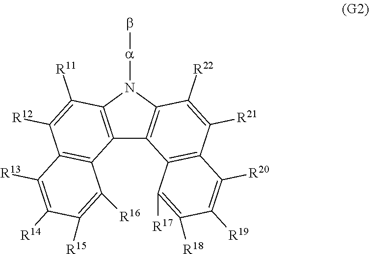
- In the general formula (G2), R11 to R22 each independently represent any of hydrogen, an alkyl group having 1 to 4 carbon atoms, and an aryl group having 6 to 12 carbon atoms, α represents a substituted or unsubstituted phenylene group, and β represents a substituted or unsubstituted anthryl group.
- In the dibenzo[c,g]carbazole compound represented by the general formula (G2), when the 7-position of a dibenzo[c,g]carbazole skeleton is bonded to the 9-position of an anthracene skeleton, the dibenzo[c,g]carbazole compound especially has a wide band gap and is effective.
- Accordingly, another structure of the present invention is a dibenzo[c,g]carbazole compound represented by the following general formula (G3).
-

- In the general formula (G3), R5 represents any of hydrogen, an alkyl group having 1 to 4 carbon atoms, and an aryl group having 6 to 10 carbon atoms, R1, R2, R3, R4, R6, R7, R8, and R9 each independently represent hydrogen or an alkyl group having 1 to 4 carbon atoms, R11 to R22 each independently represent any of hydrogen, an alkyl group having 1 to 4 carbon atoms, and an aryl group having 6 to 12 carbon atoms, and α represents a substituted or unsubstituted phenylene group.
- Furthermore, a light-emitting element using a dibenzo[c,g]carbazole compound in which the number of carbon atoms of an anthryl phenyl group bonded to a dibenzo[c,g]carbazole skeleton is 20 to 30 has element characteristics with favorable stability and reliability, which is a structure preferred in terms of evaporation in the formation of a light-emitting element.
- Accordingly, another structure of the present invention is a dibenzo[c,g]carbazole compound represented by the following general formula (G4).
-

- In the general formula (G4), R11 to R22 each independently represent any of hydrogen, an alkyl group having 1 to 4 carbon atoms, and an aryl group having 6 to 12 carbon atoms, α represents a substituted or unsubstituted phenylene group, and β represents a substituted or unsubstituted anthryl group. Note that the total number of carbon atoms of α and β is 20 to 30.
- Accordingly, another structure of the present invention is a dibenzo[c,g]carbazole compound represented by the following general formula (G5).
-

- In the general formula (G5), R5 represents any of hydrogen, an alkyl group having 1 to 4 carbon atoms, and an aryl group having 6 to 10 carbon atoms, R1, R2, R3, R4, R6, R7, R8, and R9 each independently represent hydrogen or an alkyl group having 1 to 4 carbon atoms, R11 to R22 each independently represent any of hydrogen, an alkyl group having 1 to 4 carbon atoms, and an aryl group having 6 to 12 carbon atoms, and α represents a substituted or unsubstituted phenylene group. Note that the total number of carbon atoms of R1 to R9 and α is greater than or equal to 6 and less than or equal to 16.
- Further, R1, R2, R3, R4, R6, R7, R8, and R9 are each preferably hydrogen in that synthesis becomes easy and the advantage in material cost can be obtained.
- Accordingly, another structure of the present invention is a dibenzo[c,g]carbazole compound represented by the following general formula (G6).
-

- In the general formula (G6), α represents a substituted or unsubstituted phenylene group, R5 represents any of hydrogen, an alkyl group having 1 to 4 carbon atoms, and an aryl group having 6 to 10 carbon atoms, and R11 to R22 each independently represent any of hydrogen, an alkyl group having 1 to 4 carbon atoms, and an aryl group having 6 to 12 carbon atoms. Note that the total number of carbon atoms of R5 and α is greater than or equal to 6 and less than or equal to 16.
- As in the above, R11 to R22 are each preferably hydrogen, in which case a greater advantage can be drawn.
- Accordingly, another structure of the present invention is a dibenzo[c,g]carbazole compound represented by the following general formula (G7).
-

- In the general formula (G7), α represents a substituted or unsubstituted phenylene group, and R5 represents any of hydrogen, an alkyl group having 1 to 4 carbon atoms, and an aryl group having 6 to 10 carbon atoms. Note that the total 0.5 number of carbon atoms of R5 and α is greater than or equal to 6 and less than or equal to 16.
- Another structure of the present invention is a dibenzo[c,g]carbazole compound represented by the following structural formula (100).
-

- Another structure of the present invention is a dibenzo[c,g]carbazole compound represented by the following structural formula (127).
-

- A dibenzo[c,g]carbazole compound having any of the above structures is a light-emitting element material having a wide energy gap, and can be suitably used for a transport layer, a host material, or a light-emitting substance in a blue fluorescent element or the like. In addition, the dibenzo[c,g]carbazole compound has a favorable carrier-transport property, and a light-emitting element having low driving voltage can be provided by using the compound. Further, the dibenzo[c,g]carbazole compound is stable to oxidation and reduction, and a light-emitting element manufactured using the compound can be a light-emitting element having a long lifetime which less deteriorates. Furthermore, when the dibenzo[c,g]carbazole compound has such characteristics in combination, a high-performance light-emitting element which is excellent in emission efficiency, driving voltage, and lifetime can be manufactured.
- With the use of a light-emitting element using a dibenzo[c,g]carbazole compound, a light-emitting device, a display device, a lighting device, or an electronic device each having low power consumption can be obtained. A light-emitting device, a display device, a lighting device, or an electronic device each having high reliability can also be obtained.
- In the accompanying drawings:
-
FIGS. 1A and 1B are each a conceptual diagram of a light-emitting element; -
FIG. 2 is a conceptual diagram of an organic semiconductor element; -
FIGS. 3A and 3B are conceptual diagrams of an active matrix light-emitting device; -
FIGS. 4A and 4B are conceptual diagrams of a passive matrix light-emitting device; -
FIGS. 5A and 5B are conceptual diagrams of a lighting device; -
FIGS. 6A to 6D illustrates electronic devices; -
FIG. 7 illustrates a display device; -
FIG. 8 illustrates a lighting device; -
FIG. 9 illustrates lighting devices; -
FIG. 10 illustrates in-vehicle display devices and lighting devices; -
FIGS. 11A and 11B are NMR charts of cgDBCzPA; -
FIGS. 12A and 12B each show an absorption and emission spectra of cgDBCzPA; -
FIGS. 13A and 13B are CV charts of cgDBCzPA; -
FIG. 14 shows luminance versus current efficiency characteristics of a light-emittingelement 1 and a comparison light-emittingelement 1; -
FIG. 15 shows voltage versus current characteristics of the light-emittingelement 1 and the comparison light-emittingelement 1; -
FIG. 16 shows luminance versus power efficiency characteristics of the light-emittingelement 1 and the comparison light-emittingelement 1; -
FIG. 17 shows luminance versus external quantum efficiency characteristics of the light-emittingelement 1 and the comparison light-emittingelement 1; -
FIG. 18 shows emission spectra of the light-emittingelement 1 and the comparison light-emittingelement 1; -
FIG. 19 shows normalized luminance versus time characteristics of the light-emittingelement 1 and the comparison light-emittingelement 1; -
FIG. 20 shows luminance versus current efficiency characteristics of a light-emittingelement 2 and a comparison light-emittingelement 2; -
FIG. 21 shows voltage versus current characteristics of the light-emittingelement 2 and the comparison light-emittingelement 2; -
FIG. 22 shows luminance versus power efficiency characteristics of the light-emittingelement 2 and the comparison light-emittingelement 2; -
FIG. 23 shows luminance versus external quantum efficiency characteristics of the light-emittingelement 2 and the comparison light-emittingelement 2; -
FIG. 24 shows emission spectra of the light-emittingelement 2 and the comparison light-emittingelement 2; -
FIG. 25 shows normalized luminance versus time characteristics of a light-emittingelement 2 and a comparison light-emittingelement 2; -
FIG. 26 shows luminance versus current efficiency characteristics of the light-emittingelement 3 and the comparison light-emittingelement 3; -
FIG. 27 shows voltage versus current characteristics of the light-emittingelement 3 and the comparison light-emittingelement 3; -
FIG. 28 shows emission spectra of the light-emittingelement 3 and the comparison light-emittingelement 3; -
FIG. 29 shows current density versus luminance characteristics of a light-emittingelement 4 and comparison light-emitting elements 4-1 and 4-2; -
FIG. 30 shows luminance versus current efficiency characteristics of the light-emittingelement 4 and the comparison light-emitting elements 4-1 and 4-2; -
FIG. 31 shows voltage versus current characteristics of the light-emittingelement 4 and the comparison light-emitting elements 4-1 and 4-2; -
FIG. 32 shows luminance versus power efficiency characteristics of the light-emittingelement 4 and the comparison light-emitting elements 4-1 and 4-2; -
FIG. 33 shows voltage versus luminance characteristics of the light-emittingelement 4 and the comparison light-emitting elements 4-1 and 4-2; -
FIG. 34 shows emission spectra of the light-emittingelement 4 and the comparison light-emitting elements 4-1 and 4-2; and -
FIG. 35 shows normalized luminance versus time characteristics of the light-emittingelement 4 and the comparison light-emitting elements 4-1 and 4-2. - Hereinafter, embodiments of the present invention will be described. It is easily understood by those skilled in the art that modes and details disclosed herein can be modified in various ways without departing from the spirit and scope of the present invention. Therefore, the present invention is not construed as being limited to description of the embodiments.
- A light-emitting element in this embodiment is a light-emitting element including a dibenzo[c,g]carbazole compound in which an aryl group including at least an anthracene skeleton is bonded to the 7-position of a dibenzo[c,g]carbazole skeleton. Since the dibenzo[c,g]carbazole compound has an excellent carrier-transport property, the light-emitting element can be a light-emitting element having low driving voltage. Further, since the dibenzo[c,g]carbazole compound has high resistance to repetition of oxidation and reduction, the light-emitting element can be a light-emitting element having a long lifetime. Furthermore, since the dibenzo[c,g]carbazole compound has a wide band gap, the light-emitting element can be a light-emitting element having high emission efficiency. As described above, a light-emitting element having a structure of this embodiment can easily be a high-performance light-emitting element having the right combination of characteristics.
- Note that when the number of carbon atoms of the aryl group is 14 to 30, the dibenzo[c,g]carbazole compound is a low molecular compound with a relatively low molecular weight and accordingly has a structure suitable for vacuum evaporation (capable of being vacuum-evaporated at relatively low temperature). In general, a lower molecular weight tends to diminish heat resistance after film formation. However, even with a low molecular weight, the dibenzo[c,g]carbazole compound has an advantage in that sufficient heat resistance can be ensured because of the effect of the rigid dibenzo[c,g]carbazole skeleton. Note that the anthracene skeleton and the dibenzo[c,g]carbazole skeleton described above may be bonded with an arylene group, such as a phenylene group or a naphthylene group, interposed therebetween.
- Further, a light-emitting element using a dibenzo[c,g]carbazole compound in which an anthracene skeleton is bonded to the 7-position of a dibenzo[c,g]carbazole skeleton through a phenylene group especially has the advantage in lifetime. The dibenzo[c,g]carbazole compound has an excellent carrier-transport property and a light-emitting element using this compound can be driven at very low voltage.
- The above light-emitting element can be rephrased as a light-emitting element including a dibenzo[c,g]carbazole compound in which an anthryl phenyl group is bonded to a dibenzo[c,g]carbazole skeleton. The dibenzo[c,g]carbazole compound can be easily synthesized with high purity, so that deterioration due to impurities can be suppressed. Note that the number of carbon atoms of the anthryl phenyl group bonded to the dibenzo[c,g]carbazole skeleton is preferably 20 to 30 in terms of the stability and reliability of element characteristics. In this case, the dibenzo[c,g]carbazole compound can be vacuum-evaporated at relatively low temperature as described above and accordingly is unlikely to deteriorate due to pyrolysis or the like at evaporation. In addition, the light-emitting element is excellent in not only reliability but also driving voltage. This is also because of electrochemical stability and high carrier-transport property owing to the molecular structure of the dibenzo[c,g]carbazole compound in which an anthracene skeleton is bonded to the 7-position of a dibenzo[c,g]carbazole skeleton through a phenylene group.
- Further, a light-emitting element using a dibenzo[c,g]carbazole compound in which the 9-position of an anthracene skeleton is bonded to the 7-position of a dibenzo[c,g]carbazole skeleton is particularly suitable as a light-emitting element which exhibits light emission with large energy such as blue fluorescence. Note that the anthracene skeleton and the dibenzo[c,g]carbazole skeleton described above may be bonded with an arylene group, such as a phenylene group or a naphthylene group, interposed therebetween.
- For the above reason, a light-emitting element including a dibenzo[c,g]carbazole compound in which the 9-position of an anthracene skeleton is bonded to a dibenzo[c,g]carbazole skeleton through a phenylene group is preferred. In other words, a light-emitting element including a dibenzo[c,g]carbazole compound in which a (9-anthryl)phenyl group is bonded to the 7-position of a dibenzo[c,g]carbazole skeleton is preferred. Note that the number of carbon atoms of the (9-anthryl)phenyl group bonded to the dibenzo[c,g]carbazole skeleton is preferably 20 to 30 in terms of the stability and reliability of element characteristics. Thus, the dibenzo[c,g]carbazole compound has a wide band gap which is a feature due to the effect of the skeleton of the 9-anthryl group, in addition to the high suitability for evaporation, electrochemical stability, and carrier-transport property described above. Hence, this compound is effective in a structure of a light-emitting element in which the dibenzo[c,g]carbazole compound is used as a host material of a light-emitting layer and a light-emitting material is added as a guest material to the light-emitting layer.
- In this embodiment, a dibenzo[c,g]carbazole compound used to achieve a light-emitting element described in
Embodiment 1 is described. - A dibenzo[c,g]carbazole compound of this embodiment is a dibenzo[c,g]carbazole compound in which an aryl group including at least an anthracene skeleton is bonded to the 7-position of a dibenzo[c,g]carbazole skeleton. The dibenzo[c,g]carbazole compound has an excellent carrier-transport property. In addition, the dibenzo[c,g]carbazole compound has favorable resistance to repetition of oxidation and reduction. Further, the dibenzo[c,g]carbazole compound has a wide band gap. Accordingly, a high-performance light-emitting element can be easily manufactured by including a dibenzo[c,g]carbazole compound of this embodiment.
- Note that the number of carbon atoms of the aryl group bonded to the dibenzo[c,g]carbazole skeleton is preferably 14 to 30 in terms of characteristics such as stability and reliability of the element to be fabricated. When the number of carbon atoms of the aryl group is 14 to 30, the dibenzo[c,g]carbazole compound is a low molecular compound with a relatively low molecular weight and accordingly has a structure suitable for vacuum evaporation (capable of being vacuum-evaporated at relatively low temperature). In general, a lower molecular weight tends to diminish heat resistance after film formation. However, even with a low molecular weight, the dibenzo[c,g]carbazole compound has an advantage in that sufficient heat resistance can be ensured because of the effect of the rigid dibenzo[c,g]carbazole skeleton. Note that in this specification, when the number of carbon atoms is defined, this number means the total number of carbon atoms including those of a substituent of the group, compound, or the like, of which the definition is given.
- The above dibenzo[c,g]carbazole compound can be represented by the following general formula (G1).
-

- In the above general formula (G1), Ar represents a substituted or unsubstituted aryl group which has 14 to 30 carbon atoms and includes at least an anthracene skeleton. When the anthracene skeleton has a substituent, the substituent can be an alkyl group having 1 to 4 carbon atoms. Other than such a substituent, an aryl group having 6 to 12 carbon atoms can also be selected as the substituent at the 10-position of the anthracene skeleton. Specific examples of the alkyl group having 1 to 4 carbon atoms are a methyl group, an ethyl group, a propyl group, an isopropyl group, a butyl group, an isobutyl group, a tert-butyl group, and the like. Specific examples of the aryl group having 6 to 12 carbon atoms are a phenyl group, a naphthyl group, a biphenyl group, and the like.
- Further, R11 to R22 each independently represent any of hydrogen, an alkyl group having 1 to 4 carbon atoms, and an aryl group having 6 to 12 carbon atoms. Specific examples of the alkyl group having 1 to 4 carbon atoms are a methyl group, an ethyl group, a propyl group, an isopropyl group, a butyl group, an isobutyl group, a tert-butyl group, and the like. Specific examples of the aryl group having 6 to 12 carbon atoms are a phenyl group, a naphthyl group, a biphenyl group, and the like.
- In the dibenzo[c,g]carbazole compound of this embodiment, it is preferable that the anthracene skeleton be bonded to the dibenzo[c,g]carbazole skeleton through a phenylene group, in which case the dibenzo[c,g]carbazole compound can have improved stability and can be synthesized with higher purity. Further, since the dibenzo[c,g]carbazole compound has an excellent carrier-transport property, a light-emitting element using this compound can be driven at very low voltage.
- The above dibenzo[c,g]carbazole compound can be represented by the following general formula (G2).
-

- In the general formula (G2), R11 to R22 each independently represent any of hydrogen, an alkyl group having 1 to 4 carbon atoms, and an aryl group having 6 to 12 carbon atoms. Specific examples of the alkyl group having 1 to 4 carbon atoms are a methyl group, an ethyl group, a propyl group, an isopropyl group, a butyl group, an isobutyl group, a tert-butyl group, and the like. Specific examples of the aryl group having 6 to 12 carbon atoms are a phenyl group, a naphthyl group, a biphenyl group, and the like.
- In the general formula (G2), α represents a substituted or unsubstituted phenylene group, and β represents a substituted or unsubstituted anthryl group. When a has a substituent, an alkyl group having 1 to 4 carbon atoms can be selected as the substituent. Specific examples of the alkyl group having 1 to 4 carbon atoms are a methyl group, an ethyl group, a propyl group, an isopropyl group, a butyl group, an isobutyl group, a tert-butyl group, and the like. When β has a substituent, an alkyl group having 1 to 4 carbon atoms can be selected as the substituent. Other than such a substituent, an aryl group having 6 to 12 carbon atoms can also be selected as the substituent at the 10-position of the anthracene skeleton. Specific examples of the alkyl group having 1 to 4 carbon atoms are a methyl group, an ethyl group, a propyl group, an isopropyl group, a butyl group, an isobutyl group, a tert-butyl group, and the like. Specific examples of the aryl group having 6 to 12 carbon atoms are a phenyl group, a naphthyl group, a biphenyl group, and the like.
- In the above dibenzo[c,g]carbazole compound, when the 7-position of a dibenzo[c,g]carbazole skeleton is bonded to the 9-position of an anthracene skeleton, the dibenzo[c,g]carbazole compound especially has a wide band gap and is effective. This is particularly effective in a structure of a light-emitting element in which the dibenzo[c,g]carbazole compound is used as a host material of a light-emitting layer and a light-emitting material is added as a guest material to the light-emitting layer. The above dibenzo[c,g]carbazole compound can be represented by the following general formula (G3).
-

- In the general formula (G3), R5 represents any of hydrogen, an alkyl group having 1 to 4 carbon atoms, and an aryl group having 6 to 10 carbon atoms. Specific examples of the alkyl group having 1 to 4 carbon atoms are a methyl group, an ethyl group, a propyl group, an isopropyl group, a butyl group, an isobutyl group, a tert-butyl group, and the like. Specific examples of the aryl group having 6 to 10 carbon atoms are a phenyl group, a naphthyl group, and the like. Further, R1, R2, R3, R4, R6, R7, R8, and R9 each independently represent hydrogen or an alkyl group having 1 to 4 carbon atoms. Specific examples of the alkyl group having 1 to 4 carbon atoms are a methyl group, an ethyl group, a propyl group, an isopropyl group, a butyl group, an isobutyl group, a tert-butyl group, and the like. Further, R11 to R22 each independently represent any of hydrogen, an alkyl group having 1 to 4 carbon atoms, and an aryl group having 6 to 12 carbon atoms. Specific examples of the alkyl group having 1 to 4 carbon atoms are a methyl group, an ethyl group, a propyl group, an isopropyl group, a butyl group, an isobutyl group, a tert-butyl group, and the like. Specific examples of the aryl group having 6 to 12 carbon atoms are a phenyl group, a naphthyl group, a biphenyl group, and the like. In addition, α represents a substituted or unsubstituted phenylene group. When α has a substituent, an alkyl group having 1 to 4 carbon atoms can be selected as the substituent. Specific examples of the alkyl group having 1 to 4 carbon atoms are a methyl group, an ethyl group, a propyl group, an isopropyl group, a butyl group, an isobutyl group, a tert-butyl group, and the like.
- Note that the dibenzo[c,g]carbazole compound represented by the general formula (G2) can be rephrased as a dibenzo[c,g]carbazole compound in which a phenyl anthryl group is bonded to a dibenzo[c,g]carbazole skeleton, and the dibenzo[c,g]carbazole compound represented by the general formula (G3) can be rephrased as a dibenzo[c,g]carbazole compound in which a (9-phenyl)anthryl group is bonded to a dibenzo[c,g]carbazole skeleton. Hence, the number of carbon atoms of the phenyl anthryl group or (9-phenyl)anthryl group bonded to the dibenzo[c,g]carbazole skeleton is preferably 20 to 30 in terms of characteristics such as stability and reliability of the element to be fabricated. This is probably because the dibenzo[c,g]carbazole compound can be vacuum-evaporated at relatively low temperature as described above and accordingly is unlikely to deteriorate due to pyrolysis or the like at evaporation. Note that a dibenzo[c,g]carbazole compound having a (9-phenyl)anthryl group especially has a wide band gap and therefore can be suitably used as a host material of a light-emitting layer in a light-emitting element.
- The dibenzo[c,g]carbazole compound has electrochemical stability and a high carrier-transport property owing to its molecular structure in which an anthracene skeleton is bonded to the 7-position of a dibenzo[c,g]carbazole skeleton through a phenylene group.
- The above dibenzo[c,g]carbazole compound can be represented by the following general formula (G4) or (G5).
-

- In the general formula (G4), R11 to R22 each independently represent any of hydrogen, an alkyl group having 1 to 4 carbon atoms, and an aryl group having 6 to 12 carbon atoms. Specific examples of the alkyl group having 1 to 4 carbon atoms are a methyl group, an ethyl group, a propyl group, an isopropyl group, a butyl group, an isobutyl group, a tert-butyl group, and the like. Specific examples of the aryl group having 6 to 12 carbon atoms are a phenyl group, a naphthyl group, a biphenyl group, and the like. In addition, α represents a substituted or unsubstituted phenylene group. When α has a substituent, an alkyl group having 1 to 4 carbon atoms can be selected as the substituent. Specific examples of the alkyl group having 1 to 4 carbon atoms are a methyl group, an ethyl group, a propyl group, an isopropyl group, a butyl group, an isobutyl group, a tert-butyl group, and the like. Further, β represents a substituted or unsubstituted anthryl group. When β has a substituent, an alkyl group having 1 to 4 carbon atoms can be selected as the substituent. Other than such a substituent, an aryl group having 6 to 12 carbon atoms can also be selected as the substituent at the 10-position of the anthracene skeleton. Specific examples of the alkyl group having 1 to 4 carbon atoms are a methyl group, an ethyl group, a propyl group, an isopropyl group, a butyl group, an isobutyl group, a tert-butyl group, and the like. Specific examples of the aryl group having 6 to 12 carbon atoms are a phenyl group, a naphthyl group, a biphenyl group, and the like. Note that the total number of carbon atoms of α and β is 20 to 30.
-

- In the general formula (G5), R5 represents any of hydrogen, an alkyl group having 1 to 4 carbon atoms, and an aryl group having 6 to 10 carbon atoms. Specific examples of the alkyl group having 1 to 4 carbon atoms are a methyl group, an ethyl group, a propyl group, an isopropyl group, a butyl group, an isobutyl group, a tert-butyl group, and the like. Specific examples of the aryl group having 6 to 10 carbon atoms are a phenyl group; a naphthyl group, and the like. Further, R1, R2, R3, R4, R6, R7, R8, and R9 each independently represent hydrogen or an alkyl group having 1 to 4 carbon atoms. Specific examples of the alkyl group having 1 to 4 carbon atoms are a methyl group, an ethyl group, a propyl group, an isopropyl group, a butyl group, an isobutyl group, a tert-butyl group, and the like. Further, R11 to R22 each independently represent any of hydrogen, an alkyl group having 1 to 4 carbon atoms, and an aryl group having 6 to 12 carbon atoms. Specific examples of the alkyl group having 1 to 4 carbon atoms are a methyl group, an ethyl group, a propyl group, an isopropyl group, a butyl group, an isobutyl group, a tert-butyl group, and the like. Specific examples of the aryl group having 6 to 12 carbon atoms are a phenyl group, a naphthyl group, a biphenyl group, and the like. In addition, α represents a substituted or unsubstituted phenylene group. When α has a substituent, an alkyl group having 1 to 4 carbon atoms can be selected as the substituent. Specific examples of the alkyl group having 1 to 4 carbon atoms are a methyl group, an ethyl group, a propyl group, an isopropyl group, a butyl group, an isobutyl group, a tert-butyl group, and the like. Note that the total number of carbon atoms of R1 to R9 and α is greater than or equal to 6 and less than or equal to 16.
- Further, R1, R2, R3, R4, R6, R7, R8, and R9 are each preferably hydrogen in that synthesis becomes easy and the advantage in material cost can be obtained.
- Accordingly, another structure of the present invention is a dibenzo[c,g]carbazole compound represented by the following general formula (G6).
-

- In the general formula (G6), α represents a substituted or unsubstituted phenylene group. When α has a substituent, an alkyl group having 1 to 4 carbon atoms can be selected as the substituent. Specific examples of the alkyl group having 1 to 4 carbon atoms are a methyl group, an ethyl group, a propyl group, an isopropyl group, a butyl group, an isobutyl group, a tert-butyl group, and the like. Further, R5 represents any of hydrogen, an alkyl group having 1 to 4 carbon atoms, and an aryl group having 6 to 10 carbon atoms. Specific examples of the alkyl group having. 1 to 4 carbon atoms are a methyl group, an ethyl group, a propyl group, an isopropyl group, a butyl group, an isobutyl group, a tert-butyl group, and the like. Further, R11 to R22 each independently represent any of hydrogen, an alkyl group having 1 to 4 carbon atoms, and an aryl group having 6 to 12 carbon atoms. Specific examples of the alkyl group having 1 to 4 carbon atoms are a methyl group, an ethyl group, a propyl group, an isopropyl group, a butyl group, an isobutyl group, a tert-butyl group, and the like. Note that the total number of carbon atoms of R5 and α is greater than or equal to 6 and less than or equal to 16.
- As in the above, R11 to R22 are each preferably hydrogen, in which case a greater advantage can be drawn.
- Accordingly, another structure of the present invention is a dibenzo[c,g]carbazole compound represented by the following general formula (G7).
-

- In the general formula (G7), α represents a substituted or unsubstituted phenylene group. When α has a substituent, an alkyl group having 1 to 4 carbon atoms can be selected as the substituent. Specific examples of the alkyl group having 1 to 4 carbon atoms are a methyl group, an ethyl group, a propyl group, an isopropyl group, a butyl group, an isobutyl group, a tert-butyl group, and the like. Further, R5 represents any of hydrogen, an alkyl group having 1 to 4 carbon atoms, and an aryl group having 6 to 10 carbon atoms. Specific examples of the alkyl group having 1 to 4 carbon atoms are a methyl group, an ethyl group, a propyl group, an isopropyl group, a butyl group, an isobutyl group, a tert-butyl group, and the like. Note that the total number of carbon atoms of R5 and α is greater than or equal to 6 and less than or equal to 16.
- As the aryl group represented by Ar in the above general formula (G1), for example, groups represented by structural formulae (Ar-1) to (Ar-51) below can be used. Note that a group that can be used as Ar is not limited to these.
-


- As the aryl group represented by R11 to R22 in the above general formulae (G1) to (G6), for example, groups represented by structural formulae (Rc-1) to (Rc-17) below can be used. Note that a group that can be used as R11 to R22 is not limited to these.
-


- As the aryl group represented by a in the above general formulae (G2) to (G7), for example, groups represented by structural formulae (α-1) to (α-11) below can be used. Note that a group that can be used as α is not limited to these.
-


- As the aryl group represented by β in the above general formulae (G2) and (G4), for example, groups represented by structural formulae (β-1) to (β-37) below can be used. Note that a group that can be used as β is not limited to these.
-


- As the aryl group represented by R1, R2, R3, R4, R6, R7, R5, and R9 in the above general formulae (G3) and (G5), for example, groups represented by structural formulae (Ra-1) to (Ra-9) below can be used. Note that a group that can be used as R1, R2, R3, R4, R6, R7, R8, and R9 is not limited to these.
-

- As the aryl group represented by R5 in the above general formulae (G3) and (G5) to (G7), for example, groups represented by structural formulae (R5-1) to (R5-17) below can be used. Note that a group that can be used as R5 is not limited to these.
-


- Specific examples of structures of the dibenzo[c,g]carbazole compounds represented by the above general formulae (G1) to (G7) are substances represented by structural formulae (100) to (136) below, and the like. Note that the dibenzo[c,g]carbazole compounds represented by the above general formulae (G1) to (G7) are not limited to the following examples.
-


- Since a dibenzo[c,g]carbazole compound described above has an excellent carrier-transport property, it is suitable as a carrier-transport material or a host material. Accordingly, a light-emitting element having low driving voltage can also be provided. Further, a dibenzo[c,g]carbazole compound in this embodiment has excellent stability to oxidation and reduction. Accordingly, a light-emitting element using a dibenzo[c,g]carbazole compound can be a light-emitting element having a long lifetime. Furthermore, a dibenzo[c,g]carbazole compound in this embodiment has a sufficiently wide band gap, and accordingly, even when it is used as a host material of a blue fluorescent material, a light-emitting element with high emission efficiency can be obtained.
- Next, in this embodiment, a method of synthesizing the dibenzo[c,g]carbazole compound represented by the general formula (G1) is described. A variety of reactions can be applied to the method of synthesizing the dibenzo[c,g]carbazole compound. For example, synthesis reactions described below enable the synthesis of the dibenzo[c,g]carbazole compound represented by the general formula (G1). Note that the method of synthesizing a dibenzo[c,g]carbazole compound of one embodiment of the present invention is not limited to the following synthesis methods.
- Synthesis Method of Dibenzo[c,g]carbazole Compound Represented by General Formula (G1)
- The dibenzo[c,g]carbazole compound (G1) of the present invention can be synthesized in accordance with a synthesis scheme (A-1) illustrated below. Specifically, an anthracene compound (compound 1) and a dibenzo[c,g]carbazole compound (compound 2) undergo coupling, whereby the dibenzo[c,g]carbazole compound (G1) of the present invention can be obtained.
-

- In the synthesis scheme (A-1), Ar represents a substituted or unsubstituted aryl group which has 14 to 30 carbon atoms and includes at least an anthracene skeleton. Further, R11 to R22 each independently represent any of hydrogen, an alkyl group having 1 to 4 carbon atoms, and an aryl group having 6 to 12 carbon atoms.
- In the case where a Hartwig-Buchwald reaction using a palladium catalyst is performed in the synthesis scheme (A-1), X represents a halogen or a triflate group. As the halogen, iodine, bromine, or chlorine is preferable. A palladium catalyst using a palladium compound such as bis(dibenzylideneacetone)palladium(0) or palladium(II)acetate and a ligand that coordinates to the palladium compound, such as tri(tert-butyl)phosphine, tri(n-hexyl)phosphine, or tricyclohexylphosphine, is used for the reaction. As a base, an organic base such as sodium tert-butoxide, an inorganic base such as potassium carbonate or sodium carbonate, and the like can be used for the reaction. In the case where a solvent is used, toluene, xylene, benzene, tetrahydrofuran, or the like can be used. Note that reagents which can be used for the reaction are not limited to the above.
- In the case where an Ullmann reaction using copper or a copper compound is performed in the synthesis scheme (A-1), X represents a halogen. As the halogen, iodine, bromine, or chlorine is preferable. As a catalyst, copper or a copper compound is used for the reaction. As the base which is used, an inorganic base such as potassium carbonate can be given. Examples of solvents which can be used for the reaction are 1,3-dimethyl-3,4,5,6-tetrahydro-2(1H)-pyrimidinone (DMPU), toluene, xylene, benzene, and the like. In an Ullmann reaction, DMPU or xylene, which has a high boiling point, is preferably used, in which case the object of the synthesis can be obtained in a shorter time and a higher yield at a reaction temperature of 100° C. or more. A reaction temperature of 150° C. or more is further preferred and accordingly DMPU is more preferably used. Note that reagents which can be used for the reaction are not limited to the above.
- In the above manner, a dibenzo[c,g]carbazole compound described in
Embodiment 2 can be synthesized. - In this embodiment is described an example of the mode where a dibenzo[c,g]carbazole compound described in
Embodiment 2 is used for an active layer of a vertical transistor (static induction transistor: SIT), which is a kind of an organic semiconductor element. - As illustrated in
FIG. 2 , the element has a structure in which a thin-filmactive layer 1202 containing a dibenzo[c,g]carbazole compound described inEmbodiment 2 is provided between asource electrode 1201 and adrain electrode 1203, and agate electrode 1204 is embedded in theactive layer 1202. Thegate electrode 1204 is electrically connected to a means for applying a gate voltage, and thesource electrode 1201 and thedrain electrode 1203 are electrically connected to a means for controlling a voltage between a source electrode and a drain electrode. - In such an element structure, when a voltage is applied between the source electrode and the drain electrode without applying a voltage to the gate electrode, current flows (on state). Then, by application of a voltage to the gate electrode in that state, a depletion layer is formed in the periphery of the
gate electrode 1204, and the current ceases flowing (off state). With such a mechanism, the element operates as a transistor. - Like a light-emitting element, a vertical transistor should contain a material that can achieve both a high carrier-transport property and high film quality for an active layer; a dibenzo[c,g]carbazole compound described in
Embodiment 2 meets such a requirement and therefore can be suitably used. - In this embodiment, a detailed example of the structure of a light-emitting element described in
Embodiment 1 is described below with reference toFIG. 1A . - A light-emitting element in this embodiment includes a plurality of layers between a pair of electrodes. In this embodiment, the light-emitting element includes a
first electrode 101, asecond electrode 102, and anEL layer 103, which is provided between thefirst electrode 101 and thesecond electrode 102. Note that in this embodiment, thefirst electrode 101 functions as an anode and thesecond electrode 102 functions as a cathode. In other words, when a voltage is applied between thefirst electrode 101 and thesecond electrode 102 so that the potential of thefirst electrode 101 is higher than that of thesecond electrode 102, light emission can be obtained. A light-emitting element in this embodiment is a light-emitting element in which a dibenzo[c,g]carbazole compound is used for any of layers in theEL layer 103. - For the
first electrode 101, any of metals, alloys, electrically conductive compounds, and mixtures thereof which have a high work function (specifically, a work function of 4.0 eV or more) or the like is preferably used. Specifically, for example, indium oxide-tin oxide (ITO: indium tin oxide), indium oxide-tin oxide containing silicon or silicon oxide, indium oxide-zinc oxide (indium zinc oxide), indium oxide containing tungsten oxide and zinc oxide (IWZO), and the like can be given. Films of these electrically conductive metal oxides are usually formed by sputtering but may be formed by application of a sol-gel method or the like. For example, indium oxide-zinc oxide can be formed by a sputtering method using a target in which zinc oxide is added to indium oxide at 1 wt % to 20 wt %. Moreover, indium oxide containing tungsten oxide and zinc oxide (IWZO) can be formed by a sputtering method using a target in which tungsten oxide is added to indium oxide at 0.5 wt % to 5 wt % and zinc oxide is added to indium oxide at 0.1 wt % to 1 wt %. Besides, gold (Au), platinum (Pt), nickel (Ni), tungsten (W), chromium (Cr), molybdenum (Mo), iron (Fe), cobalt (Co), copper (Cu), palladium (Pd), graphene, nitrides of metal materials (e.g., titanium nitride), and the like can be given. - There is no particular limitation on a stacked structure of the
EL layer 103. TheEL layer 103 can be formed by combining a layer that contains a substance having a high electron-transport property, a layer that contains a substance having a high hole-transport property, a layer that contains a substance having a high electron-injection property, a layer that contains a substance having a high hole-injection property, a layer that contains a bipolar substance (a substance having a high electron-transport and hole-transport property), and the like as appropriate. For example, theEL layer 103 can be formed by combining a hole-injection layer, a hole-transport layer, a light-emitting layer, an electron-transport layer, an electron-injection layer, and the like as appropriate. In this embodiment, theEL layer 103 has a structure in which a hole-injection layer 111, a hole-transport layer 112, a light-emittinglayer 113, an electron-transport layer 114, and an electron-injection layer 115 are stacked in this order over thefirst electrode 101. Materials included in the layers are specifically given below. - The hole-
injection layer 111 is a layer containing a substance having a high hole-injection property. Molybdenum oxide, vanadium oxide, ruthenium oxide, tungsten oxide, manganese oxide, or the like can be used. Alternatively, the hole-injection layer 111 can be formed with a phthalocyanine-based compound such as phthalocyanine (abbreviation: H2Pc) or copper phthalocyanine (abbreviation: CuPc), an aromatic amine compound such as 4,4′-bis[N-(4-diphenylaminophenyl)-N-phenylamino]biphenyl (abbreviation: DPAB) or N,N′-bis{4-[bis(3-methylphenyl)amino]phenyl}-N,N′-diphenyl-(1,1′-biphenyl)-4,4′-diamine (abbreviation: DNTPD), a high molecular compound such as poly(ethylenedioxythiophene)/poly(styrenesulfonic acid) (PEDOT/PSS), or the like. - Alternatively, a composite material in which a substance having a high hole-transport property contains a substance having an acceptor property can be used for the hole-
injection layer 111. Note that the use of such a substance having a high hole-transport property which contains a substance having an acceptor property enables selection of a material used to form an electrode regardless of its work function. In other words, besides a material having a high work function, a material having a low work function can also be used for thefirst electrode 101. As the substance having an acceptor property, 7,7,8,8-tetracyano-2,3,5,6-tetrafluoroquinodimethane (abbreviation: F4-TCNQ), chloranil, and the like can be given. In addition, transition metal oxides can be given. Oxides of the metals that belong toGroup 4 toGroup 8 of the periodic table can be given. Specifically, vanadium oxide, niobium oxide, tantalum oxide, chromium oxide, molybdenum oxide, tungsten oxide, manganese oxide, and rhenium oxide are preferable in that their electron-accepting property is high. Among these, molybdenum oxide is especially preferable in that it is stable in the air, has a low hygroscopic property, and is easily treated. - As the substance having a high hole-transport property used for the composite material, any of a variety of compounds such as aromatic amine compounds, carbazole derivatives, aromatic hydrocarbons, and high molecular compounds (e.g., oligomers, dendrimers, or polymers) can be used. Note that the organic compound used for the composite material is preferably an organic compound having a high hole-transport property. Specifically, a substance having a hole mobility of 10−6 cm2/Vs or more is preferably used. Further, other than these substances, any substance that has a property of transporting more holes than electrons may be used. Organic compounds that can be used as the substance having a high hole-transport property in the composite material are specifically given below.
- Examples of the aromatic amine compounds are N,N′-di(p-tolyl)-N,N′-diphenyl-p-phenylenediamine (abbreviation: DTDPPA), 4,4′-bis[N-(4-diphenylaminophenyl)-N-phenylamino]biphenyl (abbreviation: DPAB), N,N′-bis{4-[bis(3-methylphenyl)amino]phenyl}-N,N′-diphenyl-(1,1′-biphenyl)-4,4′-diamine (abbreviation: DNTPD), 1,3,5-tris[N-(4-diphenylaminophenyl)-N-phenylamino]benzene (abbreviation: DPA3B), and the like.
- Specific examples of the carbazole derivatives that can be used for the composite material are 3-[N-(9-phenylcarbazol-3-yl)-N-phenylamino]-9-phenylcarbazole (abbreviation: PCzPCA1), 3,6-bis[N-(9-phenylcarbazol-3-yl)-N-phenylamino]-9-phenylcarbazole (abbreviation: PCzPCA2), 3-[N-(1-naphthyl)-N-(9-phenylcarbazol-3-yl)amino]-9-phenylcarbazole (abbreviation: PCzPCN1), and the like.
- Other examples of the carbazole derivatives that can be used for the composite material are 4,4′-di(N-carbazolyl)biphenyl (abbreviation: CBP), 1,3,5-tris[4-(N-carbazolyl)phenyl]benzene (abbreviation: TCPB), 9-[4-(10-phenyl-9-anthryl)phenyl]-9H-carbazole (abbreviation: CzPA), 1,4-bis[4-(N-carbazolyl)phenyl]-2,3,5,6-tetraphenylbenzene, and the like.
- Examples of the aromatic hydrocarbons that can be used for the composite material are 2-tert-butyl-9,10-di(2-naphthyl)anthracene (abbreviation: t-BuDNA), 2-tert-butyl-9,10-di(1-naphthyl)anthracene, 9,10-bis(3,5-diphenylphenyl)anthracene (abbreviation: DPPA), 2-tert-butyl-9,10-bis(4-phenylphenyl)anthracene (abbreviation: t-BuDBA), 9,10-di(2-naphthyl)anthracene (abbreviation: DNA), 9,10-diphenylanthracene (abbreviation: DPAnth), 2-tert-butylanthracene (abbreviation: t-BuAnth), 9,10-bis(4-methyl-1-naphthyl)anthracene (abbreviation: DMNA), 2-tert-butyl-9,10-bis[2-(1-naphthyl)phenyl]anthracene, 9,10-bis[2-(1-naphthyl)phenyl]anthracene, 2,3,6,7-tetramethyl-9,10-di(1-naphthyl)anthracene, 2,3,6,7-tetramethyl-9,10-di(2-naphthyl)anthracene, 9,9′-bianthryl, 10,10′-diphenyl-9,9′-bianthryl, 10,10′-bis(2-phenylphenyl)-9,9′-bianthryl, 10,10′-bis[(2,3,4,5,6-pentaphenyl)phenyl]-9,9′-bianthryl, anthracene, tetracene, rubrene, perylene, 2,5,8,11-tetra(tert-butyl)perylene, and the like. Besides, pentacene, coronene, or the like can also be used. Thus, an aromatic hydrocarbon having 14 to 42 carbon atoms or more and having a hole mobility of 1×10⁻⁶ cm2/Vs is more preferably used.
- Note that the aromatic hydrocarbons that can be used for the composite material may have a vinyl skeleton. Examples of the aromatic hydrocarbon having a vinyl group are 4,4′-bis(2,2-diphenylvinyl)biphenyl (abbreviation: DPVBi), 9,10-bis[4-(2,2-diphenylvinyl)phenyl]anthracene (abbreviation: DPVPA), and the like.
- A high molecular compound such as poly(N-vinylcarbazole) (abbreviation: PVK), poly(4-vinyltriphenylamine) (abbreviation: PVTPA), poly[N-(4-{N′-[4-(4-diphenylamino)phenyl]phenyl-N′-phenylamino}phenyl)methacrylamide] (abbreviation: PTPDMA), or poly[N,N′-bis(4-butylphenyl)-N,N′-bis(phenyl)benzidine] (abbreviation: poly-TPD) can also be used.
- The hole-
transport layer 112 is a layer that contains a substance having a high hole-transport property. Examples of the substance having a high hole-transport property are aromatic amine compounds such as 4,4′-bis[N-(1-naphthyl)-N-phenylamino]biphenyl (abbreviation: NPB), N,N′-bis(3-methylphenyl)-N,N′-diphenyl-[1,1′-biphenyl]-4,4′-diamine (abbreviation: TPD), 4,4′,4″-tris(N,N-diphenylamino)triphenylamine (abbreviation: TDATA), 4,4′,4″-tris[N-(3-methylphenyl)-N-phenylamino]triphenylamine (abbreviation: MTDATA), and 4,4′-bis[N-(spiro-9,9′-bifluoren-2-yl)-N-phenylamino]biphenyl (abbreviation: BSPB), and the like. The substances mentioned here are mainly ones that have a hole mobility of 10−6 cm2/Vs or more. An organic compound given as an example of the substance having a high hole-transport property in the composite material described above can also be used for the hole-transport layer 112. A high molecular compound such as poly(N-vinylcarbazole) (abbreviation: PVK) or poly(4-vinyltriphenylamine) (abbreviation: PVTPA) can also be used. However, other than these substances, a substance that has a property of transporting more holes than electrons may be used. Further, the layer that includes a substance having a high hole-transport property is not limited to a single layer, and may be a stack of two or more layers including any of the above substances. - A dibenzo[c,g]carbazole compound described in
Embodiment 2 may be used as a material included in the hole-transport layer 112. - The light-emitting
layer 113 is a layer containing a light-emitting substance. The light-emittinglayer 113 may be formed with a film containing only a light-emitting substance or a film in which an emission center substance is dispersed into a host material. - There is no particular limitation on a material that can be used as the light-emitting substance or the emission center substance in the light-emitting
layer 113, and light emitted from the material may be either fluorescence or phosphorescence. Examples of the above light-emitting substance or emission center substance are the following substances: fluorescent substances such as N,N′-bis[4-(9-phenyl-9H-fluoren-9-yl)phenyl]-N,N′-diphenyl-pyrene-1,6-diamine (abbreviation: 1,6-FLPAPrn), N,N′-bis[4-(9H-carbazol-9-yl)phenyl]-N,N′-diphenylstilbene-4,4′-diamine (abbreviation: YGA2S), 4-(9H-carbazol-9-yl)-4′-(10-phenyl-9-anthryl)triphenylamine (abbreviation: YGAPA), 4-(9H-carbazol-9-yl)-4′-(9,10-diphenyl-2-anthryl)triphenylamine (abbreviation: 2YGAPPA), N,9-diphenyl-N-[4-(10-phenyl-9-anthryl)phenyl]-9H-carbazol-3-amine (abbreviation: PCAPA), perylene, 2,5,8,11-tetra-tert-butylperylene (abbreviation: TBP), 4-(10-phenyl-9-anthryl)-4′-(9-phenyl-9H-carbazol-3-yl)triphenylamine (abbreviation: PCBAPA), N,N″-(2-tert-butylanthracene-9,10-diyldi-4,1-phenylene)bis[N,N′,N′-triphenyl-1,4-phenylenediamine] (abbreviation: DPABPA), N,9-diphenyl-N-[4-(9,10-diphenyl-2-anthryl)phenyl]-9H-carbazol-3-amine (abbreviation: 2PCAPPA), N-[4-(9,10-diphenyl-2-anthryl)phenyl]-N,N′,N′-triphenyl-1,4-phenylenediamine (abbreviation: 2DPAPPA), N,N,N′,N′,N″,N″,N′″N′″-octaphenyldibenzo[g,p]chysene-2,7,10,15-tetraamine (abbreviation: DBC1), coumarin 30, N-(9,10-diphenyl-2-anthryl)-N,9-diphenyl-9H-carbazol-3-amine (abbreviation: 2PCAPA), N-[9,10-bis(1,1′-biphenyl-2-yl)-2-anthryl]-N,9-diphenyl-9H-carbazol-3-amine (abbreviation: 2PCABPhA), N-(9,10-diphenyl-2-anthryl)-N,N′,N′-triphenyl-1,4-phenylenediamine (abbreviation: 2DPAPA), N-[9,10-bis(1,1′-biphenyl-2-yl)-2-anthryl]-N,N′,N′-triphenyl-1,4-phenylenediamine (abbreviation: 2DPABPhA), 9,10-bis(1,1′-biphenyl-2-yl)-N-[4-(9H-carbazol-9-yl)phenyl]-N-phenylanthracen-2-amine (abbreviation: 2YGABPhA), N,N,9-triphenylanthracen-9-amine (abbreviation: DPhAPhA), coumarin 545T, N,N′-diphenylquinacridone (abbreviation: DPQd), rubrene, 5,12-bis(1,1′-biphenyl-4-yl)-6,11-diphenyltetracene (abbreviation: BPT), 2-(2-{2-[4-(dimethylamino)phenyl]ethenyl}-6-methyl-4H-pyran-4-ylidene)propanedinitrile (abbreviation: DCM1), 2-{2-methyl-6-[2-(2,3,6,7-tetrahydro-1H,5H-benzo[ij]quinolizin-9-yl)ethenyl]-4H-pyran-4-ylidene}propanedinitrile (abbreviation: DCM2), N,N,N′,N′-tetrakis(4-methylphenyl)tetracene-5,11-diamine (abbreviation: p-mPhTD), 7,14-diphenyl-N,N,N′,N′-tetrakis(4-methylphenyl)acenaphtho[1,2-α]fluoranthene-3,10-diamine (abbreviation: p-mPhAFD), 2-{2-isopropyl-6-[2-(1,1,7,7-tetramethyl-2,3,6,7-tetrahydro-1H,5H-benzo[ij]quinolizin-9-yl)ethenyl]-4H-pyran-4-ylidene}propanedinitrile (abbreviation: DCJTI), 2-{2-tert-butyl-6-[2-(1,1,7,7-tetramethyl-2,3,6,7-tetrahydro-1H,5H-benzo[j]quinolizin-9-yl)ethenyl]-4H-pyran-4-ylidene}propanedinitrile (abbreviation: DCJTB), 2-(2,6-bis{2-[4-(dimethylamino)phenyl]ethenyl}-4H-pyran-4-ylidene)propanedinitrile (abbreviation: BisDCM), and 2-{2,6-bis[2-(8-methoxy-1,1,7,7-tetramethyl-2,3,6,7-tetrahydro-1H,5H-benzo[ij]quinolizin-9-yl)ethenyl]-4H-pyran-4-ylidene}propanedinitrile (abbreviation: BisDCJTM); and phosphorescent substances such as bis[2-(3′,5′-bistrifluoromethylphenyl)pyridinato-N,C2′]iridium(III)picolinate (abbreviation: Ir(CF3ppy)2(pic)), bis[2-(4′,6′-difluorophenyl)pyridinato-N,C2′]iridium(III)acetylacetonate (abbreviation: FIracac), tris(2-phenylpyridinato)iridium(III)(abbreviation: Ir(ppy)3), bis(2-phenylpyridinato)iridium(III)acetylacetonate (abbreviation: Ir(ppy)2(acac)), tris(acetylacetonato)(monophenanthroline)terbium(III) (abbreviation: Tb(acac)3(Phen)), bis(benzo[h]quinolinato)iridium(III)acetylacetonate (abbreviation: Ir(bzq)2(acac)), bis(2,4-diphenyl-1,3-oxazolato-N,C2′)iridium(III)acetylacetonate (abbreviation: Ir(dpo)2(acac)), bis[2-(4′-perfluorophenylphenyl)pyridinato]iridium(III)acetylacetonate (abbreviation: Ir(p-PF-ph)2(acac)), bis(2-phenylbenzothiazolato-N,C2′)iridium(III)acetylacetonate (abbreviation: Ir(bt)2(acac)), bis[2-(2′-benzo[4,5-a]thienyl)pyridinato-N,C3′]iridium(III)(acetylacetonate) (abbreviation: Ir(btp)2(acac)), bis(1-phenylisoquinolinato-N,C2′)iridium(III)acetylacetonate (abbreviation: Ir(piq)2(acac)), (acetylacetonato)bis[2,3-bis(4-fluorophenyl)quinoxalinato]iridium(III) (abbreviation: Ir(Fdpq)2(acac)), (acetylacetonato)bis(2,3,5-triphenylpyrazinato)iridium(III) (abbreviation: Ir(tppr)2(acac)), 2,3,7,8,12,13,17,18-octaethyl-21H,23H-porphine platinum(II) (abbreviation: PtOEP), tris(1,3-diphenyl-1,3-propanedionato)(monophenanthroline)europium(III) (abbreviation: Eu(DBM)3 (Phen)), and tris[1-(2-thenoyl)-3,3,3-trifluoroacetonato](monophenanthroline)europium(III) (abbreviation: Eu(TTA)3(Phen)). Note that a dibenzo[c,g]carbazole compound described inEmbodiment 2 can also be used as a light-emitting material or an emission center material. The dibenzo[c,g]carbazole compound is an emission center substance which emits light having a spectrum in a range from purple to blue. - Although there is no particular limitation on a material that can be used as the host material described above, any of the following substances can be used for the host material, for example: metal complexes such as tris(8-quinolinolato)aluminum(III) (abbreviation: Alq), tris(4-methyl-8-quinolinolato)aluminum(III) (abbreviation: Almq3), bis(10-hydroxybenzo[h]quinolinato)beryllium(II) (abbreviation: BeBq2), bis(2-methyl-8-quinolinolato)(4-phenylphenolato)aluminum(III) (abbreviation: BAlq), bis(8-quinolinolato)zinc(II) (abbreviation: Znq), bis[2-(2-benzoxazolyl)phenolato]zinc(II) (abbreviation: ZnPBO), and bis[2-(2-benzothiazolyl)phenolato]zinc(II) (abbreviation: ZnBTZ); heterocyclic compounds such as 2-(4-biphenylyl)-5-(4-tert-butylphenyl)-1,3,4-oxadiazole (abbreviation: PBD), 1,3-bis[5-(p-tert-butylphenyl)-1,3,4-oxadiazol-2-yl]benzene (abbreviation: OXD-7), 3-(4-biphenylyl)-4-phenyl-5-(4-tert-butylphenyl)-1,2,4-triazole (abbreviation: TAZ), 2,2′,2″-(1,3,5-benzenetriyl)tris(1-phenyl-1H-benzimidazole) (abbreviation: TPBI), bathophenanthroline (abbreviation: BPhen), bathocuproine (abbreviation: BCP), and 9-[4-(5-phenyl-1,3,4-oxadiazol-2-yl)phenyl]-9H-carbazole (abbreviation: CO11); and aromatic amine compounds such as 4,4′-bis[N-(1-naphthyl)-N-phenylamino]biphenyl (abbreviation: NPB or α-NPD), N,N′-bis(3-methylphenyl)-N,N′-diphenyl-[1,1′-biphenyl]-4,4′-diamine (abbreviation: TPD), and 4,4′-bis[N-(spiro-9,9′-bifluoren-2-yl)-N-phenylamino]biphenyl (abbreviation: BSPB). In addition, condensed polycyclic aromatic compounds such as anthracene derivatives, phenanthrene derivatives, pyrene derivatives, chrysene derivatives, and dibenzo[g,p]chysene derivatives can be given, and specific examples are 9,10-diphenylanthracene (abbreviation: DPAnth), N,N-diphenyl-9-[4-(10-phenyl-9-anthryl)phenyl]-9H-carbazol-3-amine (abbreviation: CzA1PA), 4-(10-phenyl-9-anthryl)triphenylamine (abbreviation: DPhPA), 4-(9H-carbazol-9-yl)-4′-(10-phenyl-9-anthryl)triphenylamine (abbreviation: YGAPA), N,9-diphenyl-N-[4-(10-phenyl-9-anthryl)phenyl]-9H-carbazol-3-amine (abbreviation: PCAPA), N,9-diphenyl-N-{4-[4-(10-phenyl-9-anthryl)phenyl]phenyl}-9H-carbazol-3-amine (abbreviation: PCAPBA), N,9-diphenyl-N-(9,10-diphenyl-2-anthryl)-9H-carbazol-3-amine (abbreviation: 2PCAPA), 6,12-dimethoxy-5,11-diphenylchrysene, N,N,N′,N′,N″,N″,N′″,N′″-octaphenyldibenzo[g,p]chrysene-2,7,10,15-tetramine (abbreviation: DBC1), 9-[4-(10-phenyl-9-anthryl)phenyl]-9H-carbazole (abbreviation: CzPA), 3,6-diphenyl-9-[4-(10-phenyl-9-anthryl)phenyl]-9H-carbazole (abbreviation: DPCzPA), 9,10-bis(3,5-diphenylphenyl)anthracene (abbreviation: DPPA), 9,10-di(2-naphthyl)anthracene (abbreviation: DNA), 2-tert-butyl-9,10-di(2-naphthyl)anthracene (abbreviation: t-BuDNA), 9,9′-bianthryl (abbreviation: BANT), 9,9′-(stilbene-3,3′-diyl)diphenanthrene (abbreviation: DPNS), 9,9′-(stilbene-4,4′-diyl)diphenanthrene (abbreviation: DPNS2), 3,3′,3″-(benzene-1,3,5-triyl)tripyrene (abbreviation: TPB3), and the like. Further, a dibenzo[c,g]carbazole compound described in
Embodiment 2 can also be suitably used as a host material. One or more substances having a wider energy gap than the emission center substance described above is preferably selected from these substances and known substances. Moreover, in the case where the emission center substance is a substance which emits phosphorescence, a substance having higher triplet excitation energy (energy difference between a ground state and a triplet excitation state) than the emission center substance can be selected as the host material. - Note that a dibenzo[c,g]carbazole compound described in
Embodiment 2 can be suitably used in a light-emitting element whose emission center substance is a substance which emits blue fluorescence. This is because the wide band gap of the dibenzo[c,g]carbazole compound enables a substance which emits blue fluorescence to be effectively excited, so that a light-emitting element which provides blue fluorescence with high emission efficiency can be easily provided. Further, since a dibenzo[c,g]carbazole compound described inEmbodiment 2 has an excellent carrier-transport property, a light-emitting element having low driving voltage can be provided. - Note that the light-emitting
layer 113 can also be a stack of two or more layers. For example, in the case where the light-emittinglayer 113 is formed by stacking a first light-emitting layer and a second light-emitting layer in that order over the hole-transport layer, a substance having a hole-transport property is used for the host material of the first light-emitting layer and a substance having an electron-transport property is used for the host material of the second light-emitting layer. - In the case where the light-emitting layer having the above-described structure includes a plurality of materials, co-evaporation by a vacuum evaporation method can be used, or alternatively an inkjet method, a spin coating method, a dip coating method, or the like with a solution of the materials can be used.
- The electron-
transport layer 114 is a layer containing a substance having a high electron-transport property. For example, a layer containing a metal complex having a quinoline skeleton or a benzoquinoline skeleton, such as tris(8-quinolinolato)aluminum (abbreviation: Alq), tris(4-methyl-8-quinolinolato)aluminum (abbreviation: Almq3), bis(10-hydroxybenzo[h]quinolinato)beryllium (abbreviation: BeBq2), or bis(2-methyl-8-quinolinolato)(4-phenylphenolato)aluminum (abbreviation: BAlq). Alternatively, a metal complex having an oxazole-based or thiazole-based ligand, such as bis[2-(2-hydroxyphenyl)benzoxazolato]zinc (abbreviation: Zn(BOX)2) or bis[2-(2-hydroxyphenyl)benzothiazolato]zinc (abbreviation: Zn(BTZ)2), or the like can be used. Besides the metal complexes, 2-(4-biphenylyl)-5-(4-tert-butylphenyl)-1,3,4-oxadiazole (abbreviation: PBD), 1,3-bis[5-(p-tert-butylphenyl)-1,3,4-oxadiazol-2-yl]benzene (abbreviation: OXD-7), 3-(4-biphenylyl)-4-phenyl-5-(4-tert-butylphenyl)-1,2,4-triazole (abbreviation: TAZ), bathophenanthroline (abbreviation: BPhen), bathocuproine (abbreviation: BCP), or the like can also be used. A dibenzo[c,g]carbazole compound described inEmbodiment 2 can also be suitably used. The substances mentioned here mainly have an electron mobility of 10−6 cm2/Vs or more. Note that other than these substances, a substance that has a property of transporting more electrons than holes may be used for the electron-transport layer. - Furthermore, the electron-
transport layer 114 is not limited to a single layer and may be a stack of two or more layers containing any of the above substances. - Between the electron-transport layer and the light-emitting layer, a layer that controls transport of electron carriers may be provided. This is a layer formed by addition of a small amount of a substance having a high electron-trapping property to a material having a high electron-transport property as described above, and the layer is capable of adjusting carrier balance by suppressing transport of electron carriers. Such a structure is very effective in preventing a problem (such as a reduction in element lifetime) caused when electrons pass through the light-emitting layer.
- Since a dibenzo[c,g]carbazole compound described in
Embodiment 2 has an excellent carrier-transport property, by using the compound as a material of the electron-transport layer 114, a light-emitting element having low driving voltage can be easily provided. Further, since the dibenzo[c,g]carbazole compound has a wide band gap, even when the compound is used as a material of the electron-transport layer 114 adjacent to the light-emittinglayer 113, there is less possibility of deactivation of the excitation energy of the emission center substance and a light-emitting element with high emission efficiency can be easily provided. - In addition, an electron-
injection layer 115 may be provided in contact with thesecond electrode 102 between the electron-transport layer 114 and thesecond electrode 102. For the electron-injection layer 115, an alkali metal, an alkaline earth metal, or a compound thereof such as lithium fluoride (LiF), cesium fluoride (CsF), or calcium fluoride (CaF2) can be used. For example, a layer that is formed with a substance having an electron-transport property and contains an alkali metal, an alkaline earth metal, magnesium (Mg), or a compound thereof can be used. For example, an Alq layer containing magnesium (Mg) can be used. Note that electron injection from thesecond electrode 102 is efficiently performed with the use of a layer that is formed with a substance having an electron-transport property and contains an alkali metal or an alkaline earth metal as the electron-injection layer 115, which is preferable. - For the
second electrode 102, any of metals, alloys, electrically conductive compounds, and mixtures thereof which have a low work function (specifically, a work function of 3.8 eV or less) or the like can be used. Specific examples of such a cathode material include elements that belong toGroups second electrode 102 and the electron-transport layer, for thesecond electrode 102, any of a variety of conductive materials such as Al, Ag, ITO, or indium oxide-tin oxide containing silicon or silicon oxide can be used regardless of the work function. Films of these electrically conductive materials can be formed by a sputtering method, an inkjet method, a spin coating method, or the like. - Further, any of a variety of methods can be used to form the
EL layer 103 regardless whether it is a dry process or a wet process. For example, a vacuum evaporation method, an inkjet method, a spin coating method or the like may be used. Different formation methods may be used for the electrodes or the layers. - In addition, the electrode may be formed by a wet method using a sol-gel method, or by a wet method using paste of a metal material. Alternatively, the electrode may be formed by a dry method such as a sputtering method or a vacuum evaporation method.
- In the light-emitting element having the above-described structure, current flows due to a potential difference between the
first electrode 101 and thesecond electrode 102, and holes and electrons recombine in the light-emittinglayer 113 which contains a substance having a high light-emitting property, so that light is emitted. That is, a light-emitting region is formed in the light-emittinglayer 113. - Light emission is extracted out through one or both of the
first electrode 101 and thesecond electrode 102. Therefore, one or both of thefirst electrode 101 and thesecond electrode 102 are light-transmitting electrodes. In the case where only thefirst electrode 101 is a light-transmitting electrode, light emission is extracted through thefirst electrode 101. In the case where only thesecond electrode 102 is a light-transmitting electrode, light emission is extracted through thesecond electrode 102. In the case where both thefirst electrode 101 and thesecond electrode 102 are light-transmitting electrodes, light emission is extracted through thefirst electrode 101 and thesecond electrode 102. - The structure of the layers provided between the
first electrode 101 and thesecond electrode 102 is not limited to the above-described structure. Preferably, a light-emitting region where holes and electrons recombine is positioned away from thefirst electrode 101 and thesecond electrode 102 so that quenching due to the proximity of the light-emitting region and a metal used for electrodes and carrier-injection layers can be prevented. - Further, in order that transfer of energy from an exciton generated in the light-emitting layer can be suppressed, preferably, the hole-transport layer and the electron-transport layer which are in direct contact with the light-emitting layer, particularly a carrier-transport layer in contact with a side closer to the light-emitting region in the light-emitting
layer 113 is formed with a substance having a larger energy gap than the light-emitting substance of the light-emitting layer or the emission center substance included in the light-emitting layer. - In a light-emitting element in this embodiment, when a dibenzo[c,g]carbazole compound described in
Embodiment 2 is used for the hole-transport layer or the electron-transport layer, efficient light emission is possible even with the light-emitting substance or the emission center substance that has a large energy gap and emits blue fluorescence or green phosphorescence with large triplet excitation energy (an energy difference between a ground state and a triplet excited state); thus, a light-emitting element having high emission efficiency can be obtained. Accordingly, a light-emitting element having higher emission efficiency and lower power consumption can be provided. In addition, a light-emitting element capable of light emission with high color purity can be provided. Further, a dibenzo[c,g]carbazole compound described inEmbodiment 2 has an excellent carrier-transport property; thus, a light-emitting element having low driving voltage can be provided. - Since a dibenzo[c,g]carbazole compound described in
Embodiment 2 is stable to repetition of oxidation and reduction, a light-emitting element having a long lifetime can be easily provided by using the dibenzo[c,g]carbazole compound. - A light-emitting element in this embodiment is preferably fabricated over a substrate of glass, plastic, or the like. As the way of stacking layers over the substrate, layers may be sequentially stacked on the
first electrode 101 side or sequentially stacked on the second electrode side. - In a light-emitting device, although one light-emitting element may be formed over one substrate, a plurality of light-emitting elements may be formed over one substrate.
- With a plurality of light-emitting elements as described above formed over one substrate, a lighting device in which elements are separated or a passive-matrix light-emitting device can be manufactured.
- A light-emitting element may be formed over an electrode electrically connected to a thin film transistor (TFT), for example, which is formed over a substrate formed of glass, plastic, or the like, so that an active matrix light-emitting device in which the TFT controls the drive of the light-emitting element can be manufactured. Note that there is no particular limitation on the structure of the TFT, which may be a staggered TFT or an inverted staggered TFT. In addition, crystallinity of a semiconductor used for the TFT is not particularly limited either; an amorphous semiconductor or a crystalline semiconductor may be used. In addition, a driver circuit formed in a TFT substrate may be formed with an n-type TFT and a p-type TFT, or with either an n-type TFT or a p-type TFT.
- In this embodiment is described one mode of a light-emitting element having a structure in which a plurality of light-emitting units is stacked (hereinafter, also referred to as stacked-type element), with reference to
FIG. 1B . This light-emitting element is a light-emitting element including a plurality of light-emitting units between a first electrode and a second electrode. Each light-emitting unit can have the same structure as theEL layer 103 which is described inEmbodiment 5. In other words, the light-emitting element described inEmbodiment 5 is a light-emitting element having one light-emitting unit while the light-emitting element described inEmbodiment 6 is a light-emitting element having a plurality of light-emitting units. - In
FIG. 1B , a first light-emittingunit 511 and a second light-emittingunit 512 are stacked between afirst electrode 501 and asecond electrode 502, and acharge generation layer 513 is provided between the first light-emittingunit 511 and the second light-emittingunit 512. Thefirst electrode 501 and thesecond electrode 502 correspond, respectively, to thefirst electrode 101 and thesecond electrode 102 inEmbodiment 5, and materials described inEmbodiment 5 can be used. Further, the structures of the first light-emittingunit 511 and the second light-emittingunit 512 may be the same or different. - The
charge generation layer 513 contains a composite material of an organic compound and a metal oxide. This composite material of an organic compound and a metal oxide is the composite material described inEmbodiment 5, and contains an organic compound and a metal oxide such as vanadium oxide, molybdenum oxide, or tungsten oxide. As the organic compound, any of a variety of compounds such as aromatic amine compounds, dibenzo[c,g]carbazole compounds, carbazole compounds, aromatic hydrocarbons, and high molecular compounds (oligomers, dendrimers, polymers, or the like) can be used. Note that as the organic compound, the one having a hole mobility of 10−6 cm2/Vs or more as an organic compound having a hole-transport property is preferably used. Further, other than these substances, any substance that has a property of transporting more holes than electrons may be used. Since a composite of an organic compound and a metal oxide is excellent in carrier-injection property and carrier-transport property, low voltage driving and low current driving can be achieved. - The
charge generation layer 513 may be formed in such a way that a layer containing the composite material of an organic compound and a metal oxide is combined with a layer containing another material, for example, with a layer that contains a compound selected from substances having an electron-donating property and a compound having a high electron-transport property. Thecharge generation layer 513 may be formed in such a way that a layer containing the composite material of an organic compound and a metal oxide is combined with a transparent conductive film. - The
charge generation layer 513 provided between the first light-emittingunit 511 and the second light-emittingunit 512 may have any structure as far as electrons can be injected to a light-emitting unit on one side and holes can be injected to a light-emitting unit on the other side when a voltage is applied between thefirst electrode 501 and thesecond electrode 502. For example, inFIG. 1B , any layer can be used as thecharge generation layer 513 as far as the layer injects electrons into the first light-emittingunit 511 and holes into the second light-emittingunit 512 when a voltage is applied such that the voltage of the first electrode is higher than that of the second electrode. - Although the light-emitting element having two light-emitting units is described in this embodiment, the present invention can be similarly applied to a light-emitting element in which three or more light-emitting units are stacked. By arrangement of a plurality of light-emitting units, which are partitioned by the charge-generation layer between a pair of electrodes, as in a light-emitting element in this embodiment, light emission in a high luminance region can be realized with current density kept low, thus a light-emitting element having a long lifetime can be realized. Further, in application to lighting devices, a voltage drop due to resistance of an electrode material can be reduced and accordingly light emission in a large area is possible. Moreover, a light-emitting device having low driving voltage and lower power consumption can be realized.
- By making the light-emitting units emit light of different colors from each other, the light-emitting element can provide light emission of a desired color as a whole. For example, by forming a light-emitting element having two light-emitting units such that the emission color of the first light-emitting unit and the emission color of the second light-emitting unit are complementary colors, the light-emitting element can provide white light emission as a whole. Note that the word “complementary” means color relationship in which an achromatic color is obtained when colors are mixed. In other words, when lights obtained from substances which emit light of complementary colors are mixed, white emission can be obtained. Further, the same can be applied to a light-emitting element having three light-emitting units. For example, the light-emitting element as a whole can provide white light emission when the emission color of the first light-emitting unit is red, the emission color of the second light-emitting unit is green, and the emission color of the third light-emitting unit is blue.
- Since a light-emitting element in this embodiment includes a dibenzo[c,g]carbazole compound described in
Embodiment 2, the light-emitting element can be a light-emitting element having high emission efficiency, a light-emitting element having low driving voltage, or a light-emitting element having a long lifetime. In addition, since light emission with high color purity which is derived from the emission center substance can be obtained from the light-emitting unit including the dibenzo[c,g]carbazole compound, color adjustment of the light-emitting element as a whole is easy. - Note that this embodiment can be combined with any of the other embodiments as appropriate.
- In this embodiment, a light-emitting device using a light-emitting element including a dibenzo[c,g]carbazole compound described in Embodiment 2 (light-emitting element described in Embodiment 1) is described.
- In this embodiment, the light-emitting device using a light-emitting element including a dibenzo[c,g]carbazole compound described in Embodiment 2 (light-emitting element described in Embodiment 1) is described with reference to
FIGS. 3A and 3B . Note thatFIG. 3A is a top view illustrating the light-emitting device andFIG. 3B is a cross-sectional view ofFIG. 3A taken along the lines A-B and C-D. This light-emitting device includes a driver circuit portion (source line driver circuit) 601, apixel portion 602, and a driver circuit portion (gate line driver circuit) 603, which are to control light emission of the light-emitting element and illustrated with dotted lines. Moreover, areference numeral 604 denotes a sealing substrate; 625, a desiccant; 605, a sealing material; and 607, a space surrounded by the sealingmaterial 605. -
Reference numeral 608 denotes a wiring for transmitting signals to be inputted into the sourceline driver circuit 601 and the gateline driver circuit 603 and receiving signals such as a video signal, a clock signal, a start signal, and a reset signal from an FPC (flexible printed circuit) 609 serving as an external input terminal. Although only the FPC is illustrated here, a printed wiring board (PWB) may be attached to the FPC. The light-emitting device in the present specification includes, in its category, not only the light-emitting device itself but also the light-emitting device provided with the FPC or the PWB. - Next, a cross-sectional structure is described with reference to
FIG. 3B . The driver circuit portion and the pixel portion are formed over anelement substrate 610; the sourceline driver circuit 601, which is a driver circuit portion, and one of the pixels in thepixel portion 602 are illustrated here - As the source
line driver circuit 601, a CMOS circuit in which an n-channel TFT 623 and a p-channel TFT 624 are combined is formed. In addition, the driver circuit may be formed with any of a variety of circuits such as a CMOS circuit, a PMOS circuit, or an NMOS circuit. Although a driver integrated type in which the driver circuit is formed over the substrate is illustrated in this embodiment, the driver circuit may not necessarily be formed over the substrate, and the driver circuit can be formed outside, not over the substrate. - The
pixel portion 602 includes a plurality of pixels including a switchingTFT 611, a currentcontrolling TFT 612, and afirst electrode 613 electrically connected to a drain of the current controllingTFT 612. Note that to cover an end portion of thefirst electrode 613, aninsulator 614 is formed, for which a positive type photosensitive acrylic resin film is used here. - In order to improve coverage, the
insulator 614 is formed to have a curved surface with curvature at its upper or lower end portion. For example, in the case where positive photosensitive acrylic is used for a material of theinsulator 614, only the upper end portion of theinsulator 614 preferably has a curved surface with a curvature radius (0.2 μm to 3 μm). As theinsulator 614, either a negative photosensitive resin or a positive photosensitive resin can be used. - An
EL layer 616 and asecond electrode 617 are formed over thefirst electrode 613. Here, as a material used for thefirst electrode 613 functioning as an anode, a material having a high work function is preferably used. For example, a single-layer film of an ITO film, an indium tin oxide film containing silicon, an indium oxide film containing zinc oxide at 2 wt % to 20 wt %, a titanium nitride film, a chromium film, a tungsten film, a Zn film, a Pt film, or the like, a stack of a titanium nitride film and a film containing aluminum as its main component, a stack of three layers of a titanium nitride film, a film containing aluminum as its main component, and a titanium nitride film, or the like can be used. Note that when the stacked structure is used, thefirst electrode 613 has low resistance as a wiring, forms a favorable ohmic contact, and can function as an anode. - In addition, the
EL layer 616 is formed by any of a variety of methods such as an evaporation method using a shadow mask, an inkjet method, and a spin coating method. TheEL layer 616 includes a dibenzo[c,g]carbazole compound described inEmbodiment 2. Further, another material included in theEL layer 616 may be a low molecular compound or a high molecular compound (which may be an oligomer and a dendrimer). - As a material used for the
second electrode 617, which is formed over theEL layer 616 and functions as a cathode, a material having a low work function (e.g., Al, Mg, Li, Ca, or an alloy or compound thereof, such as MgAg, MgIn, or AlLi) is preferably used. In the case where light generated in theEL layer 616 passes through thesecond electrode 617, a stack of a thin metal film and a transparent conductive film (e.g., ITO, indium oxide containing zinc oxide at 2 wt % to 20 wt %, indium tin oxide containing silicon, or zinc oxide (ZnO)) is preferably used for thesecond electrode 617. - Note that the light-emitting element is formed with the
first electrode 613, theEL layer 616, and thesecond electrode 617. The light-emitting element has the structure described inEmbodiment 5. In the light-emitting device of this embodiment, the pixel portion, which includes a plurality of light-emitting elements, may include both the light-emitting element described inEmbodiment 1 with the structure described inEmbodiment - Further, the sealing
substrate 604 is attached to theelement substrate 610 with the sealingmaterial 605, so that a light-emittingelement 618 is provided in thespace 607 surrounded by theelement substrate 610, the sealingsubstrate 604, and the sealingmaterial 605. Thespace 607 may be filled with filler, and may be filled with an inert gas (such as nitrogen or argon), or the sealingmaterial 605. - An epoxy-based resin or glass frit is preferably used for the sealing
material 605. It is preferable that such a material do not transmit moisture or oxygen as much as possible. As the sealingsubstrate 604, a glass substrate, a quartz substrate, or a plastic substrate formed of fiberglass reinforced plastic (FRP), polyvinyl fluoride (PVF), polyester, acrylic, or the like can be used. - As described above, the light-emitting device using a light-emitting element including a dibenzo[c,g]carbazole compound described in Embodiment 2 (light-emitting element described in Embodiment 1) can be obtained.
- A light-emitting element including a dibenzo[c,g]carbazole compound described in Embodiment 2 (light-emitting element described in Embodiment 1) is used in the light-emitting device in this embodiment, and thus a light-emitting device having favorable characteristics can be obtained. Specifically, since a dibenzo[c,g]carbazole compound described in
Embodiment 2 has a large energy gap and high triplet excitation energy and can suppress energy transfer from a light-emitting substance, a light-emitting element having high emission efficiency can be provided, and accordingly a light-emitting device having reduced power consumption can be provided. In addition, a light-emitting element having low driving voltage can be provided, and accordingly a light-emitting device having low driving voltage can be provided. Further, since a light-emitting element using a dibenzo[c,g]carbazole compound described in Embodiment 2 (light-emitting element described in Embodiment 1) is a light-emitting element having a long lifetime, a light-emitting device with high reliability can be provided. - Although an active matrix light-emitting device is described in this embodiment as described above, a passive matrix light-emitting device may be manufactured.
FIGS. 4A and 4B illustrate a passive matrix light-emitting device manufactured using the present invention.FIG. 4A is a perspective view of the light-emitting device, andFIG. 4B is a cross-sectional view taken along line X-Y inFIG. 4A . InFIGS. 4A and 4B , over asubstrate 951, anEL layer 955 is provided between anelectrode 952 and anelectrode 956. An end portion of theelectrode 952 is covered with an insulatinglayer 953. In addition, apartition layer 954 is provided over the insulatinglayer 953. The sidewalls of thepartition layer 954 are aslope such that the distance between both sidewalls is gradually narrowed toward the surface of the substrate. In other words, a cross section taken along the direction of the short side of thepartition wall layer 954 is trapezoidal, and the lower side (a side which is in the same direction as a plane direction of the insulatinglayer 953 and in contact with the insulating layer 953) is shorter than the upper side (a side which is in the same direction as the plane direction of the insulatinglayer 953 and not in contact with the insulating layer 953). Thepartition layer 954 thus provided can prevent defects in the light-emitting element due to static electricity or the like. The passive matrix light-emitting device can also be driven while power consumption is kept low, by including a light-emitting element described inEmbodiment 1 which is capable of operating at low voltage and includes a dibenzo[c,g]carbazole compound described inEmbodiment 2. In addition, the light-emitting device can be driven while power consumption is kept low, by including a light-emitting element described inEmbodiment 1 which includes a dibenzo[c,g]carbazole compound described inEmbodiment 2 and accordingly has high emission efficiency. Further, the light-emitting device can have high reliability by including a light-emitting element described inEmbodiment 1 which includes a dibenzo[c,g]carbazole compound described inEmbodiment 2. - In this embodiment, an example in which a light-emitting element using a dibenzo[c,g]carbazole compound described in Embodiment 2 (light-emitting element described in Embodiment 1) is used for a lighting device is described with reference to
FIGS. 5A and 5B .FIG. 5B is a top view of the lighting device, andFIG. 5A is a cross-sectional view taken along the line E-F inFIG. 5B . - In the lighting device in this embodiment, a
first electrode 401 is formed over asubstrate 400 which is a support and has a light-transmitting property. Thefirst electrode 401 corresponds to thefirst electrode 101 inEmbodiment 5. - An
auxiliary electrode 402 is provided over thefirst electrode 401. Since light emission is extracted through thefirst electrode 401 side in the example given in this embodiment, thefirst electrode 401 is formed using a material having a light-transmitting property. Theauxiliary electrode 402 is provided in order to compensate for the low conductivity of the material having a light-transmitting property, and has a function of suppressing luminance unevenness in a light emission surface due to voltage drop caused by the high resistance of thefirst electrode 401. Theauxiliary electrode 402 is formed using a material having at least higher conductivity than the material of thefirst electrode 401, and is preferably formed using a material having high conductivity such as aluminum. Note that surfaces of theauxiliary electrode 402 other than a portion thereof in contact with thefirst electrode 401 are preferably covered with an insulating layer. With such a structure, light emission over the upper portion of theauxiliary electrode 402, which cannot be extracted, can be suppressed, so that a reduction in power efficiency due to reactive current can be suppressed. Note that apad 412 for applying a voltage to asecond electrode 404 may be formed at the same time as the formation of theauxiliary electrode 402. - An
EL layer 403 is formed over thefirst electrode 401 and theauxiliary electrode 402. TheEL layer 403 corresponds to a structure of theEL layer 103 inEmbodiment 5 or a structure combining the light-emittingunits charge generation layer 513. See the explanations of these structures. Note that theEL layer 403 is preferably formed to be slightly larger than thefirst electrode 401 when seen from above, in which case theEL layer 403 can also serve as an insulating layer that suppresses a short circuit between thefirst electrode 401 and thesecond electrode 404. - The
second electrode 404 is formed to cover theEL layer 403. Thesecond electrode 404 corresponds to thesecond electrode 102 inEmbodiment 5 and has a similar structure. In this embodiment, it is preferable that thesecond electrode 404 be formed using a material having high reflectance because light emission is extracted through thefirst electrode 401 side. In this embodiment, thesecond electrode 404 is connected to thepad 412, whereby voltage is applied. - As described above, the lighting device described in this embodiment includes a light-emitting element including the
first electrode 401, theEL layer 403, and the second electrode 404 (and the auxiliary electrode 402). Since the light-emitting element is a light-emitting element with high emission efficiency, the lighting device in this embodiment can be a lighting device having low power consumption. Further, since the light-emitting element is a light-emitting element having low driving voltage, the lighting device in this embodiment can be a lighting device having low power consumption. Furthermore, since the light-emitting element is a light-emitting element having high reliability, the lighting device in this embodiment can be a lighting device having high reliability. - The light-emitting element having the above structure is fixed to a sealing
substrate 407 with sealingmaterials material 405 or the sealingmaterial 406. In addition, theinner sealing material 406 can be mixed with a desiccant which enables moisture to be adsorbed, increasing reliability. - When extended to the outside of the sealing
materials pad 412, thefirst electrode 401, and theauxiliary electrode 402 can each partly serve as external input terminal. AnIC chip 420 mounted with a converter or the like may be provided over the external input terminals. - As described above, since the lighting device described in this embodiment includes a light-emitting element including a dibenzo[c,g]carbazole compound described in Embodiment 2 (light-emitting element described in Embodiment 1) as an EL element, the lighting device can be a lighting device having low power consumption, a lighting device with low driving voltage, or a lighting device with high reliability.
- In this embodiment, examples of an electronic device including a light-emitting element including a dibenzo[c,g]carbazole compound described in Embodiment 2 (light-emitting element described in Embodiment 1) are described. A light-emitting element including a dibenzo[c,g]carbazole compound described in Embodiment 2 (light-emitting element described in Embodiment 1) is a light-emitting element having favorable emission efficiency and reduced power consumption. Accordingly, an electronic device described in this embodiment can be an electronic device including a light-emitting portion having reduced power consumption. Further, since a light-emitting element including a dibenzo[c,g]carbazole compound described in Embodiment 2 (light-emitting element described in Embodiment 1) is a light-emitting element having low driving voltage, an electronic device described in this embodiment can be an electronic device having low driving voltage. Furthermore, since a light-emitting element including a dibenzo[c,g]carbazole compound described in Embodiment 2 (light-emitting element described in Embodiment 1) is a light-emitting element having a long lifetime, an electronic device described in this embodiment can be an electronic device having high reliability.
- Examples of the electronic devices to which the above light-emitting element is applied are television sets (also referred to as televisions or television receivers), monitors of computers or the like, cameras such as digital cameras or digital video cameras, digital photo frames, mobile phone sets (also referred to as mobile phones or mobile phone devices), portable game machines, portable information terminals, audio reproducing devices, large-sized game machines such as pachinko machines, and the like. Specific examples of these electronic devices are described below.
-
FIG. 6A illustrates an example of a television set. In the television set, adisplay portion 7103 is incorporated in ahousing 7101. In addition, here, thehousing 7101 is supported by astand 7105. Thedisplay portion 7103 enables display of images and includes light-emitting elements arranged in a matrix, each of which is a light-emitting element including a dibenzo[c,g]carbazole compound described in Embodiment 2 (light-emitting element described in Embodiment 1). The light-emitting elements can have high emission efficiency. Further, the light-emitting elements can have low driving voltage. Furthermore, the light-emitting elements can have a long lifetime. Accordingly, the television device that has thedisplay portion 7103 including the light-emitting elements can be a television device having reduced power consumption. Further, the television device can be a television device having low driving voltage. Furthermore, the television device can be a television device having high reliability. - Operation of the television set can be performed with an operation switch of the
housing 7101 or a separateremote control 7110. Withoperation keys 7109 of theremote control 7110, channels and volume can be controlled and images displayed on thedisplay portion 7103 can be controlled. Furthermore, theremote control 7110 may be provided with adisplay portion 7107 for displaying data output from theremote control 7110. - Note that the television set is provided with a receiver, a modem, and the like. With the receiver, a general television broadcast can be received. Furthermore, when the television set is connected to a communication network by wired or wireless connection via the modem, one-way (from a transmitter to a receiver) or two-way (between a transmitter and a receiver, between receivers, or the like) data communication can be performed.
-
FIG. 6B illustrates a computer having amain body 7201, ahousing 7202, adisplay portion 7203, akeyboard 7204, anexternal connection port 7205, apointing device 7206, and the like. Note that this computer is manufactured by using light-emitting elements arranged in a matrix, each of which is a light-emitting element including a dibenzo[c,g]carbazole compound described in Embodiment 2 (light-emitting element described in Embodiment 1). The light-emitting elements can have high emission efficiency. Further, the light-emitting elements can have low driving voltage. Furthermore, the light-emitting elements can have a long lifetime. Accordingly, the computer that has thedisplay portion 7203 including the light-emitting elements can be a computer having reduced power consumption. Further, the computer can be a computer having low driving voltage. Furthermore, the computer can be a computer having high reliability. -
FIG. 6C illustrates a portable game machine having two housings, ahousing 7301 and ahousing 7302, which are connected with ajoint portion 7303 so that the portable game machine can be opened or folded. Adisplay portion 7304 including light-emitting elements arranged in a matrix which are described inEmbodiment 1 and is incorporated in thehousing 7301, and adisplay portion 7305 is incorporated in thehousing 7302. Adisplay portion 7304 is incorporated in thehousing 7301, and adisplay portion 7305 is incorporated in thehousing 7302. In addition, the portable game machine illustrated inFIG. 6C includes aspeaker portion 7306, a recordingmedium insertion portion 7307, anLED lamp 7308, input means (anoperation key 7309, aconnection terminal 7310, a sensor 7311 (a sensor having a function of measuring force, displacement, position, speed, acceleration, angular velocity, rotational frequency, distance, light, liquid, magnetism, temperature, chemical substance, sound, time, hardness, electric field, current, voltage, electric power, radiation, flow rate, humidity, gradient, oscillation, odor, or infrared rays), and a microphone 7312), and the like. It is needless to say that the structure of the portable game machine is not limited to the above as far as the display portion including light-emitting elements arranged in a matrix, each of which is a light-emitting element including a dibenzo[c,g]carbazole compound described in Embodiment 2 (light-emitting element described in Embodiment 1) is used as at least either thedisplay portion 7304 or thedisplay portion 7305, or both, and the structure can include other accessories as appropriate. The portable game machine illustrated inFIG. 6C has a function of reading out a program or data stored in a storage medium to display it on the display portion, and a function of sharing information with another portable game machine by wireless communication. The portable game machine illustrated inFIG. 6C can have a variety of functions without limitation to the above. Since the light-emitting elements used in thedisplay portion 7304 have high emission efficiency, the portable game machine including the above-describeddisplay portion 7304 can be a portable game machine having reduced power consumption. Since the light-emitting elements used in thedisplay portion 7304 has low driving voltage, the portable game machine can also be a portable game machine having low driving voltage. Furthermore, since the light-emitting elements used in thedisplay portion 7304 has high reliability, the portable game machine can also be a portable game machine having high reliability. -
FIG. 6D illustrates an example of a mobile phone. A mobile phone 7400 is provided with adisplay portion 7402 incorporated in ahousing 7401,operation buttons 7403, anexternal connection port 7404, aspeaker 7405, amicrophone 7406, and the like. Note that the mobile phone 7400 is manufactured using the light-emitting device for thedisplay portion 7402. Note that the cellular phone 7400 has thedisplay portion 7402 including light-emitting elements arranged in a matrix, each of which is a light-emitting element including a dibenzo[c,g]carbazole compound described in Embodiment 2 (light-emitting element described in Embodiment 1). The light-emitting elements can have high emission efficiency. Further, the light-emitting elements can have low driving voltage. Furthermore, the light-emitting elements can have a long lifetime. Accordingly, the cellular phone that has thedisplay portion 7402 including the light-emitting elements can be a cellular phone having reduced power consumption. Further, the mobile phone can be a mobile phone having low driving voltage. Furthermore, the mobile phone can be a mobile phone having high reliability. - When the
display portion 7402 of the mobile phone 7400 illustrated inFIG. 6D is touched with a finger or the like, data can be input to the mobile phone. In this case, operations such as making a call and creating mail can be performed by touching thedisplay portion 7402 with a finger or the like. - There are mainly three screen modes of the
display portion 7402. The first mode is a display mode mainly for displaying images. The second mode is an input mode mainly for inputting data of a character and the like. The third mode is a display-and-input mode in which two modes of the display mode and the input mode are combined. - For example, in the case of making a call or creating an e-mail, a text input mode mainly for inputting a character is selected for the
display portion 7402 so that a character displayed on the screen can be input. In this case, it is preferable to display a keyboard or number buttons on almost the entire screen of thedisplay portion 7402. - When a detection device including a sensor for detecting inclination, such as a gyroscope or an acceleration sensor, is provided inside the mobile phone, display on the screen of the
display portion 7402 can be automatically switched by determining the orientation of the mobile phone (whether the mobile phone is placed horizontally or vertically for a landscape mode or a portrait mode). - The screen modes are switched by touching the
display portion 7402 or operating theoperation buttons 7403 of thehousing 7401. The screen modes can also be switched depending on the kind of image displayed on thedisplay portion 7402. For example, when a signal of an image displayed on the display portion is a signal of moving image data, the screen mode is switched to the display mode. When the signal is a signal of text data, the screen mode is switched to the input mode. - Moreover, in the input mode, when input by touching the
display portion 7402 is not performed for a certain period while a signal detected by an optical sensor in thedisplay portion 7402 is detected, the screen mode may be controlled so as to be switched from the input mode to the display mode. - The
display portion 7402 may function as an image sensor. For example, an image of a palm print, a fingerprint, or the like is taken when thedisplay portion 7402 is touched with the palm or the finger, whereby personal authentication can be performed. Further, by providing a backlight or a sensing light source which emits near-infrared light in the display portion, an image of a finger vein, a palm vein, or the like can be taken. - Note that the structure described in this embodiment can be combined with any of the structures described in
Embodiments 1 to 8 as appropriate. - As described above, the application range of the light-emitting device having a light-emitting element including a dibenzo[c,g]carbazole compound described in Embodiment 2 (light-emitting element described in Embodiment 1) is wide so that this light-emitting device can be applied to electronic devices in a variety of fields. By use of a light-emitting element including a dibenzo[c,g]carbazole compound described in
Embodiment 2, an electronic device having reduced power consumption can be obtained. In addition, an electronic device having low driving voltage can be obtained. -
FIG. 7 illustrates an example of a liquid crystal display device using a light-emitting element including a dibenzo[c,g]carbazole compound described in Embodiment 2 (light-emitting element described in Embodiment 1) for a backlight. The liquid crystal display device illustrated inFIG. 7 includes ahousing 901, aliquid crystal layer 902, abacklight 903, and ahousing 904. Theliquid crystal layer 902 is connected to adriver IC 905. A light-emitting element including a dibenzo[c,g]carbazole compound described in Embodiment 2 (light-emitting element described in Embodiment 1) is used in thebacklight 903, to which a current is supplied through a terminal 906. - A light-emitting element including a dibenzo[c,g]carbazole compound described in Embodiment 2 (light-emitting element described in Embodiment 1) is used for the backlight of the liquid crystal display device, and thus a backlight having reduced power consumption can be obtained. In addition, use of a light-emitting element including a dibenzo[c,g]carbazole compound described in
Embodiment 2 enables manufacture of a planar-emission lighting device and further a larger-area planar-emission lighting device; therefore, the backlight can be a larger-area backlight, and the liquid crystal display device can also be a larger-area device. Furthermore, the backlight using a light-emitting element including a dibenzo[c,g]carbazole compound described in Embodiment 2 (light-emitting element described in Embodiment 1) can be thinner than a conventional one; accordingly, the display device can also be thinner. -
FIG. 8 illustrates an example in which a light-emitting element including a dibenzo[c,g]carbazole compound described in Embodiment 2 (light-emitting element described in Embodiment 1) is used for a table lamp which is a lighting device. The table lamp illustrated inFIG. 8 includes ahousing 2001 and alight source 2002, and the light-emitting device described inEmbodiment 8 is used for thelight source 2002. -
FIG. 9 illustrates an example in which a light-emitting element including a dibenzo[c,g]carbazole compound described in Embodiment 2 (light-emitting element described in Embodiment 1) is used for anindoor lighting device 3001. Since a light-emitting element including a dibenzo[c,g]carbazole compound described inEmbodiment 2 has reduced power consumption, a lighting device that has reduced power consumption can be obtained. Further, since a light-emitting element including a dibenzo[c,g]carbazole compound described inEmbodiment 2 can have a large area, the light-emitting element can be used for a large-area lighting device. Furthermore, since a light-emitting element including a dibenzo[c,g]carbazole compound described inEmbodiment 2 is thin, the light-emitting element can be used for a lighting device having a reduced thickness. - A light-emitting element including a dibenzo[c,g]carbazole compound described in Embodiment 2 (light-emitting element described in Embodiment 1) can also be used for an automobile windshield or dashboard. One mode in which the light-emitting elements including a dibenzo[c,g]carbazole compound described in
Embodiment 1 are used for an automobile windshield and an automobile dashboard is illustrated inFIG. 10 .Display regions 5000 to 5005 each include a light-emitting element including a dibenzo[c,g]carbazole compound described inEmbodiment 2. - The
display region 5000 and thedisplay region 5001 are display devices which are provided in the automobile windshield and in which the light-emitting elements including a dibenzo[c,g]carbazole compound described in Embodiment 2 (i.e., each of which is a light-emitting element described in Embodiment 1) are incorporated. The light-emitting elements including a dibenzo[c,g]carbazole compound described inEmbodiment 2 can be formed into so-called see-through display devices, through which the opposite side can be seen, by including a first electrode and a second electrode formed with electrodes having a light-transmitting property. Such see-through display devices can be provided even in the automobile windshield, without hindering the vision. Note that in the case where a transistor for driving is provided, a transistor having a light-transmitting property, such as an organic transistor using an organic semiconductor material or a transistor using an oxide semiconductor, is preferably used - The
display region 5002 is a display device which is provided in a pillar portion and in which a light-emitting element including a dibenzo[c,g]carbazole compound described in Embodiment 2 (light-emitting element described in Embodiment 1) is incorporated. Thedisplay region 5002 can compensate for the view hindered by the pillar portion by showing an image taken by an imaging element provided in the automobile body. Similarly, thedisplay region 5003 provided in the dashboard can compensate for the view hindered by the automobile body by showing an image taken by an imaging element provided in the outside of the automobile body, which leads to elimination of blind areas and enhancement of safety. Showing an image so as to compensate for the area which a driver cannot see, makes it possible for the driver to confirm safety easily and comfortably. - The
display region 5004 and thedisplay region 5005 can provide a variety of kinds of information such as navigation data, a speedometer, a tachometer, a mileage, a fuel meter, a gearshift indicator, and air-condition setting. The content or layout of the display can be changed freely by a user as appropriate. Further, such information can also be shown by thedisplay regions 5000 to 5003. Note that thedisplay regions 5000 to 5005 can also be used as lighting devices. - A light-emitting element including a dibenzo[c,g]carbazole compound described in Embodiment 2 (light-emitting element described in Embodiment 1) can be a light-emitting element having low driving voltage or a light-emitting element having low power consumption. Accordingly, even when a number of large screens such as
display regions 5000 to 5005 are provided, load on a battery can be reduced, which provides comfortable use. The light-emitting device and the lighting device each using a light-emitting element including a dibenzo[c,g]carbazole compound described inEmbodiment 2 can be suitably used as an in-vehicle light-emitting device or lighting device. - In this example, a synthesis method of 7-[4-(10-phenyl-9-anthryl)phenyl]-7H-dibenzo[c,g]carbazole (abbreviation: cgDBCzPA), which is a dibenzo[c,g]carbazole compound represented by the general formula (G1) described in
Embodiment 2, is described in detail. - In a 100 mL three-neck flask were placed 1.0 g (20 mmol) of hydrazine monohydrate and 14 mL ethanol. To this solution in an ice bath was added dropwise 2.2 mL of a 1.7 M acetic acid aqueous solution with a dropping funnel. To this solution were added dropwise 10 g (68 mmol) of β-tetralone dissolved in 10 mL ethanol with a dropping funnel. This mixture was stirred at 80° C. for 7 hours, whereby a solid was precipitated. After the stirring, this mixture was added to about 50 mL of water and the mixture was stirred at room temperature for 30 minutes. After the stirring, this mixture was suction-filtered to collect a solid. Methanol/water in a 1:1 ratio was added to the collected solid and the mixture was irradiated with ultrasonic waves, and a solid was washed. After the washing, this mixture was suction-filtered and a solid was collected, giving 3.5 g of a yellow powder in a yield of 63%. A reaction scheme (a-1) of
Step 1 is illustrated below. -

- In a 200 mL three-neck flask were placed 6.2 g of chloranil (25 mmol), 40 mL of xylene, and 3.5 g (12 mmol) of 5,6,8,9-tetrahydro-7H-benzo[c,g]carbazole suspended in 20 mL of xylene. This mixture was refluxed at 150° C. for 4 hours under a nitrogen stream. After reaction, this mixture cooled to room temperature, precipitating a solid. The precipitated solid was removed by suction filtration and a filtrate was obtained. The obtained filtrate was purified by silica gel column chromatography (developing solvent: toluene/hexane in a 2:1 ratio) to give a red solid. Recrystallization of the obtained solid from toluene/hexane gave pale-red needle-like crystals. The obtained crystals were again recrystallized from toluene/hexane, so that 2.5 g of white needle-like crystals were obtained in 78% yield. A reaction scheme (b-1) of
Step 2 is illustrated below. -

- In a 100 mL three-neck flask were placed 2.3 g (5.6 mmol) of 9-(4-bromophenyl)-10-phenylanthracene, 1.5 g (5.6 mol) of 7H-dibenzo[c,g]carbazole, and 1.2 g (12 mmol) of sodium tert-butoxide. After the air in the flask was replaced with nitrogen, to this mixture were added 30 mL of toluene and 2.8 mL of tri-(tert-butyl)phosphine (a 10 wt % hexane solution). This mixture was degassed by being stirred while the pressure was reduced. After the degassing, 0.16 g (0.28 mmol) of bis(dibenzylideneacetone)palladium(0) was added to this mixture. This mixture was stirred at 110° C. for 17 hours under a nitrogen stream, so that a solid was precipitated. The precipitated solid was removed by suction filtration. The collected solid was dissolved in about 30 mL of hot toluene, and this solution was suction-filtered through Celite (produced by Wako Pure Chemical Industries, Ltd., Catalog No. 531-16855), alumina, and Florisil (produced by Wako Pure Chemical Industries, Ltd., Catalog No. 540-00135). A solid obtained by concentration of the filtrate was recrystallized from toluene/hexane to give 2.3 g of a pale yellow powder, which was the object of the synthesis, in a yield of 70%. A reaction scheme (c-1) of
Step 3 is illustrated below. -

- By a train sublimation method, 2.3 g of the obtained pale yellow powdery solid was purified by sublimation. In the sublimation purification, cgDBCzPA was heated at 310° C. under a pressure of 3.6 Pa with a flow rate of argon at 6.0 mL/min. After the sublimation purification, 2.1 g of a pale yellow solid of cgDBCzPA was recovered in 91% yield.
- The obtained substance was measured by 1H NMR. The measurement data are shown below.
- 1H NMR (CDCl3, 300 MHz): δ=7.38-7.67 (m, 11H), 7.72-7.89 (m, 12H), 7.96 (d, J=8.7 Hz, 2H), 8.10 (d, J=7.2 Hz, 2H), 9.31 (d, J1=8.1 Hz, 2H)
- In addition,
FIGS. 11A and 11B are 1H-NMR charts. The measurement results show that 7-[4-(10-phenyl-9-anthryl)phenyl]-7H-dibenzo[c,g]carbazole (abbreviation: cgDBCzPA) represented by the above structural formula was obtained. - Next, absorption and emission spectra of cgDBCzPA in a toluene solution of cgDBCzPA are shown in
FIG. 12A , and absorption and emission spectra of a thin film of cgDBCzPA are shown inFIG. 12B . The absorption spectra were measured using an ultraviolet-visible light spectrophotometer (V550 type manufactured by Japan Spectroscopy Corporation). A toluene solution of cgDBCzPA was put in a quartz cell and an absorption spectrum of cgDBCzPA in the toluene solution was measured. From this absorption spectrum, an absorption spectrum of the toluene solution measured with the quartz cell was subtracted, and the resultant value was shown in the drawing. In addition, as for the absorption spectrum of the thin film, a sample was prepared by evaporation of cgDBCzPA over a quartz substrate, and the absorption spectrum obtained by subtraction of an absorption spectrum of quartz from the absorption spectrum of this sample is shown in the drawing. As in the measurements of the absorption spectra, an ultraviolet-visible spectrophotometer (V550, manufactured by JASCO Corporation) was used for the measurements of the emission spectra. The emission spectrum of cgDBCzPA in a toluene solution of cgDBCzPA was measured with the toluene solution of cgDBCzPA put in a quartz cell, and the emission spectrum of the thin film was measured with a sample prepared by evaporation of cgDBCzPA over a quartz substrate. These show that the maximum absorption wavelengths of cgDBCzPA in the toluene solution of cgDBCzPA were around 396 nm, around 368 nm, around 351 nm, around 306 nm, and around 252 nm and that the maximum emission wavelengths thereof were around 417 nm and around 432 nm (an excitation wavelength of 369 nm). These also show that the maximum absorption wavelengths of the thin film were around 402 nm, around 375 nm, around 357 nm, around 343 nm, around 306 nm, around 268 nm, around 252 nm, and around 221 nm and that the largest maximum emission wavelength thereof was around 442 nm (an excitation wavelength of 402 nm). - Further, the ionization potential of a thin film of cgDBCzPA was measured by a photoelectron spectrometer (AC-2, manufactured by Riken Keiki, Co., Ltd.) in the air. The obtained value of the ionization potential was converted to a negative value, revealing that the HOMO level of cgDBCzPA was −5.72 eV. From the data of the absorption spectra of the thin film in
FIGS. 12A and 12B , the absorption edge of cgDBCzPA, which was obtained from a Tauc plot with an assumption of direct transition, was 2.95 eV. Therefore, the optical energy gap of cgDBCzPA in the solid state was estimated at 2.95 eV; from the values of the HOMO level obtained above and this energy gap, the LUMO level of cgDBCzPA was able to be estimated at −2.77 eV. It was thus found that cgDBCzPA had a wide energy gap of 2.95 eV in the solid state. - The oxidation characteristics and reduction characteristics of cgDBCzPA were measured. These were examined by cyclic voltammetry (CV) measurements. An electrochemical analyzer (ALS model 600A or 600C, manufactured by BAS Inc.) was used for the measurements.
- Further, as for a solution used for the CV measurements, dehydrated dimethylformamide (DMF, manufactured by Sigma-Aldrich Inc., 99.8%, Catalog No. 22705-6) was used as a solvent, and tetra-n-butylammonium perchlorate (n-Bu4NClO4, manufactured by Tokyo Chemical Industry Co., Ltd., Catalog No. T0836), which was a supporting electrolyte, was dissolved in the solvent such that the concentration was 100 mmol/L. Further, the object to be measured was dissolved in the solvent such that the concentration was 2 mmol/L. A platinum electrode (PTE platinum electrode, manufactured by BAS Inc.) was used as a working electrode, a platinum electrode (Pt counter electrode for VC-3 (5 cm), manufactured by BAS Inc.) was used as an auxiliary electrode, and an Ag/Ag+ electrode (RE-5 reference electrode for nonaqueous solvent, manufactured by BAS Inc.) was used as a reference electrode. Note that the measurements were conducted at room temperature (20 to 25° C.). The scan rate was set to 0.1 V/s through the CV measurements.
- In the measurements of the oxidation characteristics, one cycle was scanning in which the potential of the working electrode with respect to the reference electrode was changed from 0.05 V to 0.83 V and then changed from 0.83 V to 0.05 V, and 100-cycle measurements were performed. Measurement results were shown in
FIG. 13A . - The measurement results revealed that cgDBCzPA showed properties effective against repetition of redox reactions between an oxidized state and a neutral state without large variations in oxidation peak even after the 100-cycle measurements.
- In the measurements of the reduction characteristics, one cycle was scanning in which the potential of the working electrode with respect to the reference electrode was changed from −1.50 V to −2.30 V and then changed from −2.30 V to −1.50 V, and 100-cycle measurements were performed. Measurement results were shown in
FIG. 13B . - The measurement results revealed that cgDBCzPA showed properties effective against repetition of redox reactions between a reduced state and a neutral state without large variations in reduction peak even after the 100 cycles in the measurements.
- Further, the HOMO and LUMO levels of cgDBCzPA were calculated also from the CV measurement results.
- First, the potential energy of the reference electrode with respect to the vacuum level used was found to be −4.94 eV. According to the measurement results of the oxidation characteristics of cgDBCzPA, the oxidation peak potential Epa was 0.81 V and the reduction peak potential Epc was 0.69 V. Therefore, a half-wave potential (an intermediate potential between Epa and Epc) can be determined at 0.75 V. This means that cgDBCzPA is oxidized by an electric energy of 0.75 [V vs. Ag/Ag+], and this energy corresponds to the HOMO level. Here, since the potential energy of the reference electrode, which was used in this example, with respect to the vacuum level is −4.94 [eV] as described above, the HOMO level of cgDBCzPA was found to be as follows: −4.94−0.75=−5.69 [eV]. According to the measurement results of the reduction characteristics of cgDBCzPA, the oxidation peak potential Epc was −2.25 V and the reduction peak potential Epa was −2.16 V. Therefore, a half-wave potential (an intermediate potential between Epc and Epa) can be calculated at −2.21 V. This means that cgDBCzPA is reduced by an electric energy of −2.21 [V vs. Ag/Ag+], and this energy corresponds to the LUMO level. Here, since the potential energy of the reference electrode, which was used in this example, with respect to the vacuum level is −4.94 [eV] as described above, the LUMO level of cgDBCzPA was found to be as follows: −4.94−(−2.21)=−2.74 [eV].
- Note that the potential energy of the reference electrode (Ag/Ag+ electrode) with respect to the vacuum level corresponds to the Fermi level of the Ag/Ag+ electrode, and should be calculated from a value obtained by measuring a substance whose potential energy with respect to the vacuum level is known, with the use of the reference electrode (Ag/Ag+ electrode).
- How the potential energy (eV) of the reference electrode (Ag/Ag+ electrode), which was used in this example, with respect to the vacuum level is determined by calculation is specifically described. It is known that the oxidation-reduction potential of ferrocene in methanol is +0.610 [V vs. SHE] with respect to the standard hydrogen electrode (Reference: Christian R. Goldsmith et al., J. Am. Chem. Soc., Vol. 124, No. 1, pp. 83-96, 2002). In contrast, using the reference electrode used in this example, the oxidation-reduction potential of ferrocene in methanol was calculated at +0.11 V [vs. Ag/Ag+]. Thus, it was found that the potential energy of this reference electrode was lower than that of the standard hydrogen electrode by 0.50 [eV].
- Here, it is known that the potential energy of the standard hydrogen electrode with respect to the vacuum level is −4.44 eV (Reference: Toshihiro Ohnishi and Tamami Koyama, High molecular EL material, Kyoritsu shuppan, pp. 64-67). Therefore, the potential energy of the reference electrode used in this example with respect to the vacuum level can be calculated as follows: −4.44−0.50=−4.94 [eV].
- In this example is described a light-emitting element using a dibenzo[c,g]carbazole compound, 7-[4-(10-phenyl-9-anthryl)phenyl]-7H-dibenzo[c,g]carbazole (abbreviation: cgDBCzPA, structural formula (100)), as a host material of a light-emitting layer using an emission center substance which emits blue fluorescence and as a material of an electron-transport layer, which is a light-emitting element described in
Embodiment 1. - The molecular structures of organic compounds used in this example are illustrated in structural formulae (i) to (iv) and (100) below. The element structure was similar to that illustrated in
FIG. 1A . -


- First, a glass substrate over which indium tin oxide containing silicon (ITSO) had been formed to a thickness of 110 nm was prepared as the
first electrode 101. A surface of the ITSO was covered with a polyimide film so that an area of 2 mm×2 mm of the surface was exposed. The electrode area was 2 mm×2 mm. As pretreatment for forming the light-emitting element over this substrate, UV ozone treatment was performed for 370 seconds after washing of a surface of the substrate with water and baking that was performed at 200° C. for 1 hour. After that, the substrate was transferred into a vacuum evaporation apparatus where the pressure had been reduced to approximately 10−4 Pa, and was subjected to vacuum baking at 170° C. for 30 minutes in a heating chamber of the vacuum evaporation apparatus, and then the substrate was cooled down for about 30 minutes. - Next, the substrate was fixed to a holder provided in the vacuum evaporation apparatus so that the surface of the substrate over which the ITSO film was formed faced downward.
- After the pressure in the vacuum evaporation apparatus was reduced to 10−4 Pa, 9-phenyl-3-[4-(10-phenyl-9-anthryl)phenyl]-9H-carbazole (abbreviation: PCzPA) represented by the above structural formula (i) and molybdenum(VI)oxide were co-evaporated so that the ratio of PCzPA to molybdenum oxide was 2:1 (weight ratio), thereby forming the hole-
injection layer 111. The thickness of the hole-injection layer 111 was set to 70 nm. Note that co-evaporation is an evaporation method in which a plurality of different substances is concurrently vaporized from the respective different evaporation sources. - Next, PCzPA was evaporated to a thickness of 30 nm, so that the hole-
transport layer 112 was formed. - Further, over the hole-
transport layer 112, 7-[4-(10-phenyl-9-anthryl)phenyl]-7H-dibenzo[c,g]carbazole (abbreviation: cgDBCzPA) represented by the above structural formula (100) and N,N′-bis(3-methylphenyl)-N,N′-bis[3-(9-phenyl-9H-fluoren-9-yl)phenyl]-pyrene-1,6-diamine (abbreviation: 1,6mMemFLPAPrn) represented by the above structural formula (iii) were co-evaporated to a thickness of 25 nm so that the ratio of cgDBCzPA to 1,6mMemFLPAPrn was 1:0.03 (weight ratio), thereby forming the light-emittinglayer 113. - Next, cgDBCzPA was evaporated to a thickness of 10 nm, and then bathophenanthroline (abbreviation: BPhen) represented by the above structural formula (iv) was evaporated to a thickness of 15 nm, thereby forming the electron-
transport layer 114. - Further, lithium fluoride was evaporated to a thickness of 1 nm over the electron-
transport layer 114, thereby forming the electron-injection layer. Lastly, aluminum was formed to a thickness of 200 nm as thesecond electrode 102 which serves as a cathode. Thus, the light-emittingelement 1 was completed. Note that in all the above evaporation steps, evaporation was performed by a resistance-heating method. - The comparison light-emitting
element 1 was formed like the light-emittingelement 1, except for the light-emittinglayer 113 and the electron-transport layer 114. As to the light-emittinglayer 113, after the hole-transport layer 112 was formed, 9-[4-(10-phenyl-9-anthryl)phenyl]-9H-carbazole (abbreviation: CzPA) represented by the above structural formula (ii) and N,N′-bis(3-methylphenyl)-N,N′-bis[3-(9-phenyl-9H-fluoren-9-yl)phenyl]-pyrene-1,6-diamine (abbreviation: 1,6mMemFLPAPm) represented by the above structural formula (iii) were co-evaporated to a thickness of 25 nm so that the ratio of CzPA to 1,6mMemFLPAPrn was 1:0.05 (weight ratio), thereby forming the light-emittinglayer 113. - After the light-emitting
layer 113 was formed, CzPA was evaporated to a thickness of 10 nm, and then bathophenanthroline (abbreviation: BPhen) represented by the above structural formula (iv) was evaporated to a thickness of 15 nm, thereby forming the electron-transport layer 114. - The structure other than the light-emitting
layer 113 and the electron-transport layer 114 is similar to that of the light-emittingelement 1, and repetition of the explanation of the structure is avoided. Refer to the fabrication method of the light-emittingelement 1. - Thus, the comparison light-emitting
element 1 was completed. - The light-emitting
element 1 and the comparison light-emittingelement 1 obtained as described above were sealed in a glove box containing a nitrogen atmosphere so as not to be exposed to the air (specifically, a sealing material was applied onto an outer edge of each element and heat treatment was performed at 80° C. for 1 hour at the time of sealing). Then, the operating characteristics of the light-emitting elements were measured. Note that the measurements were carried out at room temperature (in an atmosphere in which the temperature was kept at 25° C.). -
FIG. 14 shows luminance versus current efficiency characteristics of the light-emittingelement 1 and the comparison light-emittingelement 1,FIG. 15 shows voltage versus current characteristics,FIG. 16 shows luminance versus power efficiency characteristics, andFIG. 17 shows luminance versus external quantum efficiency characteristics. InFIG. 14 , the vertical axis represents current efficiency (cd/A) and the horizontal axis represents luminance (cd/m2). InFIG. 15 , the vertical axis represents current (mA) and the horizontal axis represents voltage (V). InFIG. 16 , the vertical axis represents power efficiency (lm/W) and the horizontal axis represents luminance (cd/m2). InFIG. 17 , the vertical axis represents external quantum efficiency (%) and the horizontal axis represents luminance (cd/m2). - As can be seen from
FIG. 14 , the luminance versus current efficiency characteristics of the light-emittingelement 1 that provides blue fluorescence and uses cgDBCzPA, which is a dibenzo[c,g]carbazole compound represented by the general formula (G1), as a host material of a light-emitting layer and as an electron-transport material of an electron-transport layer are favorable or substantially equal to the luminance versus current efficiency characteristics of the comparison light-emittingelement 1 using CzPA like cgDBCzPA in the light-emittingelement 1. This indicates that the light-emittingelement 1 is a light-emitting element having high emission efficiency. - As can be seen from
FIG. 15 , the voltage versus current characteristics of the light-emittingelement 1 are favorable or substantially equal to those of the comparison light-emittingelement 1, which indicates that the light-emittingelement 1 is a light-emitting element having low driving voltage. This means that the dibenzo[c,g]carbazole compound represented by the general formula (G1) has an excellent carrier-transport property. - As can be seen from
FIG. 16 , the light-emittingelement 1 exhibits better luminance versus power efficiency characteristics than the light-emittingelement 1, which indicates that the light-emittingelement 1 is a light-emitting element having low power consumption. Thus, the light-emittingelement 1 using cgDBCzPA, which is a dibenzo[c,g]carbazole compound represented by the general formula (G1), is a light-emitting element having favorable characteristics such as low driving voltage and high emission efficiency. - As can be seen from
FIG. 17 , the luminance versus external quantum efficiency characteristics of the light-emittingelement 1 are favorable and substantially equal to those of the comparison light-emittingelement 1, which indicates that the light-emittingelement 1 is a light-emitting element having high emission efficiency. -
FIG. 18 shows emission spectra obtained when a current of 0.1 mA was made to flow in the fabricated light-emittingelement 1 and the comparison light-emittingelement 1. InFIG. 18 , the vertical axis represents emission intensity (arbitrary unit) and the horizontal axis represents wavelength (nm). The emission intensity is shown as a value relative to the maximum emission intensity assumed to be 1.FIG. 18 indicates that both the light-emittingelement 1 and the comparison light-emittingelement 1 emit blue light emission derived from 1,6mMemFLPAPrn, which was the emission center substance. - Next, with an initial luminance set to 5000 cd/m2, the light-emitting
element 1 and the comparison light-emittingelement 1 were driven under a condition where the current density was constant, and changes in luminance relative to driving time were examined.FIG. 19 shows normalized luminance versus time characteristics.FIG. 19 indicates that, although the comparison light-emittingelement 1 using CzPA is a light-emitting element having a long lifetime, the light-emittingelement 1 using cgDBCzPA is an extremely reliable element having a longer lifetime than the comparison light-emittingelement 1. - As compared with CzPA, cgDBCzPA is highly stable to evaporation and can easily provide a light-emitting element having stable qualities.
- As described above, cgDBCzPA is found to be a material with which a light-emitting element having the right combination of excellent characteristics can be provided.
- In this example is described a light-emitting element using a dibenzo[c,g]carbazole compound, 7-[4-(10-phenyl-9-anthryl)phenyl]-7H-dibenzo[c,g]carbazole (abbreviation: cgDBCzPA, structural formula (100)), as a host material of a light-emitting layer using an emission center substance which emits blue fluorescence and as a material of an electron-transport layer, which is a light-emitting element described in
Embodiment 1. - The molecular structures of organic compounds used in this example are illustrated in structural formulae (i) to (v) and (100) below. The element structure was similar to that illustrated in
FIG. 1A . -


- First, a glass substrate over which indium tin oxide containing silicon (ITSO) had been formed to a thickness of 110 nm was prepared as the
first electrode 101. A surface of the ITSO was covered with a polyimide film so that an area of 2 mm×2 mm of the surface was exposed. The electrode area was 2 mm×2 mm. As pretreatment for forming the light-emitting element over this substrate, UV ozone treatment was performed for 370 seconds after washing of a surface of the substrate with water and baking that was performed at 200° C. for 1 hour. After that, the substrate was transferred into a vacuum evaporation apparatus where the pressure had been reduced to approximately 10−4 Pa, and was subjected to vacuum baking at 170° C. for 30 minutes in a heating chamber of the vacuum evaporation apparatus, and then the substrate was cooled down for about 30 minutes. - Next, the substrate was fixed to a holder provided in the vacuum evaporation apparatus so that the surface of the substrate over which the ITSO film was formed faced downward.
- After the pressure in the vacuum evaporation apparatus was reduced to 10−4 Pa, 9-phenyl-3-[4-(10-phenyl-9-anthryl)phenyl]-9H-carbazole (abbreviation: PCzPA) represented by the above structural formula (i) and molybdenum(VI)oxide were co-evaporated so that the ratio of PCzPA to molybdenum oxide was 2:1 (weight ratio), thereby forming the hole-
injection layer 111. The thickness of the hole-injection layer 111 was set to 70 nm. Note that co-evaporation is an evaporation method in which a plurality of different substances is concurrently vaporized from the respective different evaporation sources. - Next, 3-[4-(9-phenanthryl)-phenyl]-9-phenyl-9H-carbazole (abbreviation: PCPPn) represented by the above structural formula (v) was evaporated to a thickness of 30 nm, so that the hole-
transport layer 112 was formed. - Further, over the hole-
transport layer 112, 7-[4-(10-phenyl-9-anthryl)phenyl]-7H-dibenzo[c,g]carbazole (abbreviation: cgDBCzPA) represented by the above structural formula (100) and N,N′-bis(3-methylphenyl)-N,N′-bis[3-(9-phenyl-9H-fluoren-9-yl)phenyl]-pyrene-1,6-diamine (abbreviation: 1,6mMemFLPAPrn) represented by the above structural formula (iii) were co-evaporated to a thickness of 25 nm so that the ratio of cgDBCzPA to 1,6mMemFLPAPrn was 1:0.03 (weight ratio), thereby forming the light-emittinglayer 113. - Next, cgDBCzPA was evaporated to a thickness of 10 nm, and then bathophenanthroline (abbreviation: BPhen) represented by the above structural formula (iv) was evaporated to a thickness of 15 nm, thereby forming the electron-
transport layer 114. - Further, lithium fluoride was evaporated to a thickness of 1 nm over the electron-
transport layer 114, thereby forming the electron-injection layer. Lastly, aluminum was formed to a thickness of 200 nm as thesecond electrode 102 which serves as a cathode. Thus, the light-emittingelement 2 was completed. Note that in all the above evaporation steps, evaporation was performed by a resistance-heating method. - The comparison light-emitting
element 2 was formed like the light-emittingelement 2, except for the light-emittinglayer 113 and the electron-transport layer 114. As to the light-emittinglayer 113, after the hole-transport layer 112 was formed, 9-[4-(10-phenyl-9-anthryl)phenyl]-9H-carbazole (abbreviation: CzPA) represented by the above structural formula (ii) and N,N′-bis(3-methylphenyl)-N,N′-bis[3-(9-phenyl-9H-fluoren-9-yl)phenyl]-pyrene-1,6-diamine (abbreviation: 1,6mMemFLPAPrn) represented by the above structural formula (iii) were co-evaporated to a thickness of 25 nm so that the ratio of CzPA to 1,6mMemFLPAPrn was 1:0.05 (weight ratio), thereby forming the light-emittinglayer 113. - After the light-emitting
layer 113 was formed, CzPA was evaporated to a thickness of 10 nm, and then bathophenanthroline (abbreviation: BPhen) represented by the above structural formula (iv) was evaporated to a thickness of 15 nm, thereby forming the electron-transport layer 114. - The structure other than the light-emitting
layer 113 and the electron-transport layer 114 is similar to that of the light-emittingelement 2, and repetition of the explanation of the structure is avoided. Refer to the fabrication method of the light-emittingelement 2. - Thus, the comparison light-emitting
element 2 was completed. - The light-emitting
element 2 and the comparison light-emittingelement 2 obtained as described above were sealed in a glove box containing a nitrogen atmosphere so as not to be exposed to the air (specifically, a sealing material was applied onto an outer edge of each element and heat treatment was performed at 80° C. for 1 hour at the time of sealing). Then, the operating characteristics of the light-emitting elements were measured. Note that the measurements were carried out at room temperature (in an atmosphere in which the temperature was kept at 25° C.). -
FIG. 20 shows luminance versus current efficiency characteristics of the light-emittingelement 2 and the comparison light-emittingelement 2,FIG. 21 shows voltage versus current characteristics,FIG. 22 shows luminance versus power efficiency characteristics, andFIG. 23 shows luminance versus external quantum efficiency characteristics. InFIG. 20 , the vertical axis represents current efficiency (cd/A) and the horizontal axis represents luminance (cd/m2). InFIG. 21 , the vertical axis represents current (mA) and the horizontal axis represents voltage (V). InFIG. 22 , the vertical axis represents power efficiency (lm/W) and the horizontal axis represents luminance (cd/m2). InFIG. 23 , the vertical axis represents external quantum efficiency (%) and the horizontal axis represents luminance (cd/m2). - As can be seen from
FIG. 20 , the luminance versus current efficiency characteristics of the light-emittingelement 2 that provides blue fluorescence and uses cgDBCzPA, which is a dibenzo[c,g]carbazole compound represented by the general formula (G1), as a host material of a light-emitting layer and as an electron-transport material of an electron-transport layer are substantially equal to the luminance versus current efficiency characteristics of the comparison light-emittingelement 2 using CzPA like cgDBCzPA in the light-emittingelement 2. This indicates that the light-emittingelement 2 is a light-emitting element having high emission efficiency. - As can be seen from
FIG. 21 , the light-emittingelement 2 exhibits better voltage versus current characteristics than the light-emittingelement 2, which indicates that the light-emittingelement 2 is a light-emitting element having low driving voltage. This means that the dibenzo[c,g]carbazole compound represented by the general formula (G1) has an excellent carrier-transport property. - As can be seen from
FIG. 22 , the light-emittingelement 2 exhibits very favorable luminance versus power efficiency characteristics better than those of the comparison light-emittingelement 2, which indicates that the light-emittingelement 2 is a light-emitting element having low power consumption. Thus, the light-emittingelement 2 using cgDBCzPA which is a dibenzo[c,g]carbazole compound represented by the general formula (G1) is a light-emitting element having favorable characteristics such as low driving voltage and high emission efficiency. - As can be seen from
FIG. 23 , the luminance versus external quantum efficiency characteristics of the light-emittingelement 2 are favorable and substantially equal to those of the comparison light-emittingelement 2, which indicates that the light-emittingelement 2 is a light-emitting element having very high emission efficiency. -
FIG. 24 shows emission spectra obtained when a current of 0.1 mA was made to flow in the fabricated light-emittingelement 2 and the comparison light-emittingelement 2. InFIG. 24 , the vertical axis represents emission intensity (arbitrary unit) and the horizontal axis represents wavelength (nm). The emission intensity is shown as a value relative to the maximum emission intensity assumed to be 1.FIG. 24 shows the spectra of the light-emittingelement 2 and the comparison light-emittingelement 2 overlaps completely, which indicates that both elements emit blue light emission derived from 1,6mMemFLPAPrn, which was the emission center substance. - Next, with an initial luminance set to 5000 cd/m2, the light-emitting
element 2 and the comparison light-emittingelement 2 were driven under a condition where the current density was constant, and changes in luminance relative to driving time were examined.FIG. 25 shows normalized luminance versus time characteristics.FIG. 25 indicates that, although the comparison light-emittingelement 2 using CzPA is a light-emitting element having a long lifetime, the light-emittingelement 2 using cgDBCzPA is an extremely reliable element having a longer lifetime than the comparison light-emittingelement 2. - As compared with CzPA, cgDBCzPA is highly stable to evaporation and can easily provide a light-emitting element having stable qualities.
- As described above, it is also confirmed in this example that cgDBCzPA is found to be a material with which a light-emitting element having the right combination of excellent characteristics can be provided.
- In this example is described a light-emitting element using a dibenzo[c,g]carbazole compound, 7-[4-(10-phenyl-9-anthryl)phenyl]-7H-dibenzo[c,g]carbazole (abbreviation: cgDBCzPA, structural formula (100)), as a host material of a light-emitting layer using an emission center substance which emits blue fluorescence and as a material of an electron-transport layer, which is a light-emitting element described in
Embodiment 1. - The molecular structures of organic compounds used in this example are illustrated in structural formulae (i) to (vi) and (100) below. The element structure was similar to that illustrated in
FIG. 1A . -


- First, a glass substrate over which indium tin oxide containing silicon (ITSO) had been formed to a thickness of 110 nm was prepared as the
first electrode 101. A surface of the ITSO was covered with a polyimide film so that an area of 2 mm×2 mm of the surface was exposed. The electrode area was 2 min×2 mm. As pretreatment for forming the light-emitting element over this substrate, UV ozone treatment was performed for 370 seconds after washing of a surface of the substrate with water and baking that was performed at 200° C. for 1 hour. After that, the substrate was transferred into a vacuum evaporation apparatus where the pressure had been reduced to approximately 10−4 Pa, and was subjected to vacuum baking at 170° C. for 30 minutes in a heating chamber of the vacuum evaporation apparatus, and then the substrate was cooled down for about 30 minutes. - Next, the substrate was fixed to a holder provided in the vacuum evaporation apparatus so that the surface of the substrate over which the ITSO film was formed faced downward.
- After the pressure in the vacuum evaporation apparatus was reduced to 10−4 Pa, 9-phenyl-3-[4-(10-phenyl-9-anthryl)phenyl]-9H-carbazole (abbreviation: PCzPA) represented by the above structural formula (i) and molybdenum(VI)oxide were co-evaporated so that the ratio of PCzPA to molybdenum oxide was 2:1 (weight ratio), thereby forming the hole-
injection layer 111. The thickness of the hole-injection layer 111 was set to 50 nm. Note that co-evaporation is an evaporation method in which a plurality of different substances is concurrently vaporized from the respective different evaporation sources. - Next, PCzPA was evaporated to a thickness of 10 nm, so that the hole-
transport layer 112 was formed. - Further, over the hole-
transport layer 112, 7-[4-(10-phenyl-9-anthryl)phenyl]-7H-dibenzo[c,g]carbazole (abbreviation: cgDBCzPA) represented by the above structural formula (100) and N,N′-bis(3-methylphenyl)-N,N′-bis[3-(9-phenyl-9H-fluoren-9-yl)phenyl]-pyrene-1,6-diamine (abbreviation: 1,6mMemFLPAPrn) represented by the above structural formula (iii) were co-evaporated to a thickness of 30 nm so that the ratio of cgDBCzPA to 1,6mMemFLPAPrn was 1:0.05 (weight ratio), thereby forming the light-emittinglayer 113. - Next, tris(8-quinolinolato)aluminum(III) (abbreviation: Alq) represented by the above structural formula (vi) was evaporated to a thickness of 10 nm, and then bathophenanthroline (abbreviation: BPhen) represented by the above structural formula (iv) was evaporated to a thickness of 15 nm; thereby forming the electron-
transport layer 114. - Further, lithium fluoride was evaporated to a thickness of 1 nm over the electron-
transport layer 114, thereby forming the electron-injection layer. Lastly, aluminum was formed to a thickness of 200 nm as thesecond electrode 102 which serves as a cathode. Thus, the light-emittingelement 3 was completed. Note that in all the above evaporation steps, evaporation was performed by a resistance-heating method. - The comparison light-emitting
element 3 was formed like the light-emittingelement 3, except for the light-emittinglayer 113. For the comparison light-emittingelement 3, after the hole-transport layer 112 was formed, 9-[4-(10-phenyl-9-anthryl)phenyl]-9H-carbazole (abbreviation: CzPA) represented by the above structural formula (ii) and N,N′-bis(3-methylphenyl)-N,N′-bis[3-(9-phenyl-9H-fluoren-9-yl)phenyl]-pyrene-1,6-diamine (abbreviation: 1,6mMemFLPAPrn) represented by the above structural formula (iii) were co-evaporated to a thickness of 30 nm so that the ratio of CzPA to 1,6mMemFLPAPrn was 1:0.05 (weight ratio), thereby forming the light-emittinglayer 113. - The structure other than the light-emitting
layer 113 is similar to that of the light-emittingelement 3, and repetition of the explanation of the structure is avoided. Refer to the fabrication method of the light-emittingelement 3. - Thus, the comparison light-emitting
element 3 was completed. - The light-emitting
element 3 and the comparison light-emittingelement 3 obtained as described above were sealed in a glove box containing a nitrogen atmosphere so as not to be exposed to the air (specifically, a sealing material was applied onto an outer edge of each element and heat treatment was performed at 80° C. for 1 hour at the time of sealing). Then, the operating characteristics of the light-emitting elements were measured. Note that the measurements were carried out at room temperature (in an atmosphere in which the temperature was kept at 25° C.). -
FIG. 26 shows luminance versus current efficiency characteristics of the light-emitting,element 3 and the comparison light-emittingelement 3, andFIG. 27 shows voltage versus current characteristics. InFIG. 26 , the vertical axis represents current efficiency (cd/A) and the horizontal axis represents luminance (cd/m2). InFIG. 27 , the vertical axis represents current (mA) and the horizontal axis represents voltage (V). - As can be seen from
FIG. 26 , the luminance versus current efficiency characteristics of the light-emittingelement 3 that provides blue fluorescence and uses cgDBCzPA, which is a dibenzo[c,g]carbazole compound represented by the general formula (G1), as a host material of a light-emitting layer and as an electron-transport material of an electron-transport layer are equal to the luminance versus current efficiency characteristics of the comparison light-emittingelement 3 using CzPA like cgDBCzPA in the light-emittingelement 3. This indicates that the light-emittingelement 3 is a light-emitting element having high emission efficiency. - As can be seen from
FIG. 27 , the light-emittingelement 3 has much better voltage versus current characteristics than the comparison light-emittingelement 3, which indicates that the light-emittingelement 3 is a light-emitting element having low driving voltage. This means that the dibenzo[c,g]carbazole compound represented by the general formula (G1) has an excellent carrier-transport property. -
FIG. 28 shows emission spectra obtained when a current of 0.1 mA was made to flow in the fabricated light-emittingelement 3 and the comparison light-emittingelement 3. InFIG. 28 , the vertical axis represents emission intensity (arbitrary unit) and the horizontal axis represents wavelength (nm). The emission intensity is shown as a value relative to the maximum emission intensity assumed to be 1.FIG. 28 shows the spectra of the light-emittingelement 3 and the comparison light-emittingelement 3 are not greatly different, which indicates that both elements emit blue light emission derived from 1,6mMemFLPAPrn, which was the emission center substance. - As compared with CzPA, cgDBCzPA is highly stable to evaporation and can easily provide a light-emitting element having stable qualities.
- As described above, it is also confirmed in this example that cgDBCzPA is found to be a material with which a light-emitting element having the right combination of excellent characteristics can be provided.
- In this example is described a light-emitting element using a dibenzo[c,g]carbazole compound, 7-[4-(10-phenyl-9-anthryl)phenyl]-7H-dibenzo[c,g]carbazole (abbreviation: cgDBCzPA, structural formula (100)), as a host material of a light-emitting layer using an emission center substance which emits blue fluorescence and as a material of an electron-transport layer, which is a light-emitting element described in
Embodiment 1. - The molecular structures of organic compounds used in this example are illustrated in structural formulae (i), (iii), (iv), (vi) to (viii), and (100) below. The element structure was similar to that illustrated in
FIG. 1A . -


- First, a glass substrate over which indium tin oxide containing silicon (ITSO) had been formed to a thickness of 110 nm was prepared as the
first electrode 101. A surface of the ITSO was covered with a polyimide film so that an area of 2 mm×2 mm of the surface was exposed. The electrode area was 2 mm×2 mm. As pretreatment for forming the light-emitting element over this substrate, UV ozone treatment was performed for 370 seconds after washing of a surface of the substrate with water and baking that was performed at 200° C. for 1 hour. After that, the substrate was transferred into a vacuum evaporation apparatus where the pressure had been reduced to approximately 10−4 Pa, and was subjected to vacuum baking at 170° C. for 30 minutes in a heating chamber of the vacuum evaporation apparatus, and then the substrate was cooled down for about 30 minutes. - Next, the substrate was fixed to a holder provided in the vacuum evaporation apparatus so that the surface of the substrate over which the ITSO film was formed faced downward.
- After the pressure in the vacuum evaporation apparatus was reduced to 10−4 Pa, 9-phenyl-3-[4-(10-phenyl-9-anthryl)phenyl]-9H-carbazole (abbreviation: PCzPA) represented by the above structural formula (i) and molybdenum(VI)oxide were co-evaporated so that the ratio of PCzPA to molybdenum oxide was 2:1 (weight ratio), thereby forming the hole-
injection layer 111. The thickness of the hole-injection layer 111 was set to 50 nm. Note that co-evaporation is an evaporation method in which a plurality of different substances is concurrently vaporized from the respective different evaporation sources. - Next, PCzPA was evaporated to a thickness of 10 nm, so that the hole-
transport layer 112 was formed. - Further, over the hole-
transport layer 112, 7-[4-(10-phenyl-9-anthryl)phenyl]-7H-dibenzo[c,g]carbazole (abbreviation: cgDBCzPA) represented by the above structural formula (100) and N,N′-bis(3-methylphenyl)-N,N′-bis[3-(9-phenyl-9H-fluoren-9-yl)phenyl]-pyrene-1,6-diamine (abbreviation: 1,6mMemFLPAPrn) represented by the above structural formula (iii) were co-evaporated to a thickness of 25 nm so that the ratio of cgDBCzPA to 1,6mMemFLPAPrn was 1:0.03 (weight ratio), thereby forming the light-emittinglayer 113. - Next, tris(8-quinolinolato)aluminum(III) (abbreviation: Alq) represented by the above structural formula (vi) was evaporated to a thickness of 10 nm, and then bathophenanthroline (abbreviation: BPhen) represented by the above structural formula (iv) was evaporated to a thickness of 15 nm, thereby forming the electron-
transport layer 114. - Further, lithium fluoride was evaporated to a thickness of 1 nm over the electron-
transport layer 114, thereby forming the electron-injection layer. Lastly, aluminum was formed to a thickness of 200 nm as thesecond electrode 102 which serves as a cathode. Thus, the light-emittingelement 4 was completed. Note that in all the above evaporation steps, evaporation was performed by a resistance-heating method. - The comparison light-emitting element 4-1 was formed like the light-emitting
element 4, except for the light-emittinglayer 113. For the comparison light-emitting element 4-1, after the hole-transport layer 112 was formed, a known anthracene derivative represented by the above structural formula (vii) and N,N′-bis(3-methylphenyl)-N,N′-bis[3-(9-phenyl-9H-fluoren-9-yl)phenyl]-pyrene-1,6-diamine (abbreviation: 1,6mMemFLPAPrn) represented by the above structural formula (iii) were co-evaporated to a thickness of 25 nm so that the ratio of the anthracene derivative to 1,6mMemFLPAPrn was 1:0.03 (weight ratio), thereby forming the light-emittinglayer 113. - The structure other than the light-emitting
layer 113 is similar to that of the light-emittingelement 4, and repetition of the explanation of the structure is avoided. Refer to the fabrication method of the light-emittingelement 4. - Thus, the comparison light-emitting element 4-1 was completed.
- The comparison light-emitting element 4-2 was formed like the light-emitting
element 4, except for the light-emittinglayer 113. For the comparison light-emitting element 4-2, after the hole-transport layer 112 was formed, a known anthracene derivative represented by the above structural formula (viii) and N,N′-bis(3-methylphenyl)-N,N′-bis[3-(9-phenyl-9H-fluoren-9-yl)phenyl]-pyrene-1,6-diamine (abbreviation: 1,6mMemFLPAPrn) represented by the above structural formula (iii) were co-evaporated to a thickness of 25 nm so that the ratio of the anthracene derivative to 1,6mMemFLPAPrn was 1:0.03 (weight ratio), thereby forming the light-emittinglayer 113. - The structure other than the light-emitting
layer 113 is similar to that of the light-emittingelement 4, and repetition of the explanation of the structure is avoided. Refer to the fabrication method of the light-emittingelement 4. - Thus, the comparison light-emitting element 4-2 was completed.
- The light-emitting
element 4 and the comparison light-emitting elements 4-1 and 4-2 obtained as described above were sealed in a glove box containing a nitrogen atmosphere so as not to be exposed to the air (specifically, a sealing material was applied onto an outer edge of each element and heat treatment was performed at 80° C. for 1 hour at the time of sealing). Then, the operating characteristics of the light-emitting elements were measured. Note that the measurements were carried out at room temperature (in an atmosphere in which the temperature was kept at 25° C.). -
FIG. 29 shows current density versus luminance characteristics of the light-emittingelement 4 and the comparison light-emitting elements 4-1 and 4-2,FIG. 30 shows luminance versus current efficiency characteristics,FIG. 31 shows voltage versus current characteristics,FIG. 32 shows luminance versus power efficiency characteristics, andFIG. 33 shows voltage versus luminance characteristics. InFIG. 29 , the vertical axis represents luminance (cd/m2) and the horizontal axis represents current density (mA/cm2). InFIG. 30 , the vertical axis represents current efficiency (cd/A) and the horizontal axis represents luminance (cd/m2). InFIG. 31 , the vertical axis represents current (mA) and the horizontal axis represents voltage (V). InFIG. 32 , the vertical axis represents power efficiency (lm/W) and the horizontal axis represents luminance (cd/m2). InFIG. 33 , the vertical axis represents luminance (cd/m2) and the horizontal axis represents voltage (V). - As can be seen from
FIG. 29 , the light-emittingelement 4 and the comparison light-emitting elements 4-1 and 4-2 have substantially equal current density versus luminance characteristics. In addition,FIG. 30 reveals that the light-emittingelement 4 and the comparison light-emitting elements 4-1 and 4-2 have substantially equal luminance versus current efficiency characteristics, at a luminance of at least 1000 cd/m2 or more which is a practical luminance. - Furthermore,
FIG. 31 reveals that the light-emittingelement 4 exhibits much better voltage versus current characteristics than the comparison light-emitting elements 4-1 and 4-2. This indicates the favorable carrier-transport property of cgDBCzPA. Thus, also as seen fromFIG. 32 , the light-emittingelement 4 is found to be an element having highly favorable luminance versus power efficiency characteristics. Note thatFIG. 33 shows high driving voltage of the comparison light-emitting elements 4-1 and 4-2, and in order to achieve a luminance of 1000 cd/m2, which is of practical use, a voltage of about 3.3 V needs to be applied to the light-emittingelement 4 but a voltage of 4 V or more needs to be applied to each of the comparison light-emitting elements 4-1 and 4-2. The driving voltage of the comparison light-emitting element 4-1 is especially high. -
FIG. 34 shows emission spectra obtained when a current of 0.1 mA was made to flow in the fabricated light-emittingelement 4 and the comparison light-emitting element 4-1 and 4-2. InFIG. 34 , the vertical axis represents emission intensity (arbitrary unit) and the horizontal axis represents wavelength (nm). The emission intensity is shown as a value relative to the maximum emission intensity assumed to be 1.FIG. 34 shows the spectra of the light-emittingelement 4 and the comparison light-emitting element 4-1 and 4-2 are not greatly different, which indicates that both elements emit blue light emission derived from 1,6mMemFLPAPrn, which was the emission center substance. - Next, with an initial luminance set to 5000 cd/m2, the light-emitting
element 4 and the comparison light-emitting elements 4-1 and 4-2 were driven under a condition where the current density was constant, and changes in luminance relative to driving time were examined.FIG. 35 shows normalized luminance versus time characteristics.FIG. 35 shows that the comparison light-emitting element 4-2 using the substance represented by the above structural formula (viii) has a shorter lifetime than the other elements. In addition, although the comparison light-emitting element 4-1 using the substance represented by the above structural formula (vii) instead of cgDBCzPA has a lifetime equal to that of the light-emittingelement 4 at a glance, the comparison light-emitting element 4-1 exhibits not only a rise in initial luminance but also an increase in deterioration rate after a certain time point; consequently, the half life of the comparison light-emitting element 4-1 is estimated at about half of that of the light-emittingelement 4. - Thus, the comparison light-emitting element 4-1 has a drawback in driving voltage and the comparison light-emitting element 4-2 has drawbacks in both driving voltage and lifetime, and it is difficult for each element to have the right combination of characteristics. In contrast, by using cgDBCzPA, a high-performance light-emitting element which has excellent combination of characteristics in terms of efficiency, driving voltage, and lifetime is found to be able to be fabricated. What is remarkable is the driving voltage, which enables a light-emitting element having very high power efficiency to be provided.
- As described above, it is also confirmed in this example that cgDBCzPA is found to be a material with which a light-emitting element having the right combination of excellent characteristics can be provided.
- In this example is described a synthesis method of 7-[4-(10-phenyl-9-anthryl)phenyl]-7H-dibenzo[c,g]carbazole (abbreviation: cgDBCzPA), which is a dibenzo[c,g]carbazole compound represented by the general formula (G1) described in
Embodiment 2, which is different from the synthesis method in Example 1. - The steps up to and including synthesis of 7H-dibenzo[c,g]carbazole were the same as
Steps - In a 200 mL three-neck flask were placed 5.0 g (18 mmol) of 7H-dibenzo[c,g]carbazole, 13 g (47 mol) of 4-bromoiodobenzene, and 1.9 g (20 mmol) of sodium tert-butoxide. After the air in the flask was replaced with nitrogen, to this mixture were added 100 mL of mesitylene and 0.90 mL of tri-(tert-butyl)phosphine (a 10 wt % hexane solution). This mixture was degassed by being stirred while the pressure was reduced. After the degassing, 0.51 g (0.90 mmol) of bis(dibenzylideneacetone)palladium(0) was added to this mixture. This mixture was stirred at 170° C. for 17 hours under a nitrogen stream. After the stirring, 20 mL of water was added to the obtained mixture. The aqueous layer of this mixture was extracted with toluene, and the solution of the extract and the organic layer were combined and washed with saturated brine. The organic layer was dried with magnesium sulfate, and this mixture was gravity-filtered. A solid obtained by concentration of the obtained filtrate was dissolved in about 30 mL of toluene. This solution was suction-filtered through Celite (manufactured by Wako Pure Chemical Industries, Ltd., Catalog No. 531-16855), alumina, and Florisil (manufactured by Wako Pure Chemical Industries, Ltd., Catalog No. 540-00135). A solid obtained by concentration of the filtrate was recrystallized from toluene/hexane to give 2.9 g of pale yellow needle-like crystals, which was the object of the synthesis, in a yield of 38% yield. A reaction scheme (c-2) of
Step 3 is illustrated below. -

- In a 200 mL three-neck flask were placed 1.7 g (4.0 mmol) of 7-(4-bromophenyl)-7H-dibenzo[c,g]carbazole and 1.2 g (4.0 mmol) of 10-phenylanthracene-9-boronic acid, and the air in the flask was replaced with nitrogen. To this mixture were added 15 mL of toluene, 5.0 mL of ethanol, and 4.0 mL of an aqueous solution of sodium carbonate. This mixture was degassed by being stirred while the pressure was reduced. To this mixture was added 0.23 g (0.20 mmol) of tetrakis(triphenylphosphine)palladium(0), and the mixture was stirred at 90° C. for 10 hours under a nitrogen stream, so that a solid was precipitated. The precipitated solid was removed by suction filtration. The collected solid was dissolved in about 50 mL of hot toluene, and this solution was suction-filtered through Celite (produced by Wako Pure Chemical Industries, Ltd., Catalog No. 531-16855), alumina, and Florisil (produced by Wako Pure Chemical Industries, Ltd., Catalog No. 540-00135). A solid obtained by concentration of the filtrate was washed with toluene/hexane to give 1.3 g of a pale yellow powder, which was the object of the synthesis, in a yield of 55%. A synthesis scheme (d-2) of
Step 4 is illustrated below. -

- By a train sublimation method, 1.3 g of the obtained pale yellow powdery solid was purified by sublimation. In the sublimation purification, cgDBCzPA was heated at 300° C. under a pressure of 3.6 Pa with a flow rate of argon at 5.0 mL/min. After the sublimation purification, 1.1 g of a pale yellow solid of cgDBCzPA was recovered in 86% yield.
- A method of synthesizing N,N′-bis(3-methylphenyl)-N,N′-bis[3-(9-phenyl-9H-fluoren-9-yl)phenyl]-pyrene-1,6-diamine (abbreviation: 1,6mMemFLPAPrn) used in the above examples is described.
- There were placed 3.2 g (8.1 mmol) of 9-(3-bromophenyl)-9-phenylfluorene and 2.3 g (24.1 mmol) of sodium tert-butoxide in a 200 mL three-neck flask. The air in the flask was replaced with nitrogen. Then, 40.0 mL of toluene, 0.9 mL (8.3 mmol) of m-toluidine, and 0.2 mL of a 10% hexane solution of tri(tert-butyl)phosphine were added to this mixture. The temperature of this mixture was set to 60° C., and 44.5 mg (0.1 mmol) of bis(dibenzylideneacetone)palladium(0) was added to the mixture. The temperature of the mixture was raised to 80° C., and the mixture was stirred for 2.0 hours. After the stirring, the mixture was suction-filtered through Florisil (produced by Wako Pure Chemical Industries, Ltd., Catalog No. 540-00135), Celite (produced by Wako Pure Chemical Industries, Ltd., Catalog No. 531-16855), and alumina to give a filtrate. The filtrate was concentrated to give a solid, which was then purified by silica gel column chromatography (developing solvent: hexane/toluene in a 1:1 ratio). Recrystallization from a mixed solvent of toluene and hexane gave 2.8 g of a white solid, which was the object of the synthesis, in 82% yield. A synthesis scheme of the
above Step 1 is illustrated below. -

- There were placed 0.6 g (1.7 mmol) of 1,6-dibromopyrene, 1.4 g (3.4 mmol) of 3-methylphenyl-3-(9-phenyl-9H-fluoren-9-yl)phenylamine obtained in
Step 1 above, and 0.5 g (5.1 mmol) of sodium tert-butoxide in a 100 mL three-neck flask. The air in the flask was replaced with nitrogen. To this mixture were added 21.0 mL of toluene and 0.2 mL of a 10% hexane solution of tri(tert-butyl)phosphine. The temperature of this mixture was set to 60° C., and 34.9 mg (0.1 mmol) of bis(dibenzylideneacetone)palladium(0) was added to the mixture. The temperature of this mixture was set to 80° C., and the mixture was stirred for 3.0 hours. After the stirring, 400 mL of toluene was added to the mixture, and the mixture was heated. While the mixture it was suction-filtered through Florisil (produced by Wako Pure Chemical Industries, was kept hot, Ltd., Catalog No. 540-00135), Celite (produced by Wako Pure Chemical Industries, Ltd., Catalog No. 531-16855), and alumina to give a filtrate. The filtrate was concentrated to give a solid, which was then purified by silica gel column chromatography (developing solvent: hexane/toluene in a 3:2 ratio) to give a yellow solid. Recrystallization of the obtained yellow solid from a mixed solvent of toluene and hexane gave 1.2 g of a yellow solid, which was the object of the synthesis, in 67% yield. - By a train sublimation method, 1.0 g of the obtained yellow solid was purified. In the purification, the yellow solid was heated at 317° C. under a pressure of 2.2 Pa with a flow rate of argon gas of 5.0 mL/min. After the purification, 1.0 g of a yellow solid, which was the object of the synthesis, in 93% yield. A synthesis scheme of the
above Step 2 is illustrated below. -

- A nuclear magnetic resonance (NMR) spectroscopy identified this compound as N,N′-bis(3-methylphenyl)-N,N′-bis[3-(9-phenyl-9H-fluoren-9-yl)phenyl]-pyrene-1,6-diamine (abbreviation: 1,6mMemFLPAPrn), which was the object of the synthesis.
- 1H NMR data of the obtained compound are shown below.
- 1H NMR (CDCl3, 300 MHz): δ=2.21 (s, 6H), 6.67 (d, J=7.2 Hz, 2H), 6.74 (d, J=7.2 Hz, 2H), 7.17-7.23 (m, 34H), 7.62 (d, J=7.8 Hz, 4H), 7.74 (d, J=7.8 Hz, 2H), 7.86 (d, J=9.0 Hz, 2H), 8.04 (d, J=8.7 Hz, 4H).
- An example of synthesis of 3-[4-(9-phenanthryl)-phenyl]-9-phenyl-9H-carbazole (abbreviation: PCPPn) is described.
-

- In a 300 mL three-neck flask, 8.0 g (20 mmol) of 3-(4-bromophenyl)-9-phenyl-9H-carbazole was placed, the air in the flask was replaced with nitrogen, 100 mL of dehydrated tetrahydrofuran (abbreviation: THF) was added, and the temperature was lowered to −78° C. Into this mixture solution, 15 mL (24 mmol) of a 1.65 mol/L n-butyllithium hexane solution was dropped, and the mixture solution with the n-butyllithium hexane solution added was stirred for 2 hours. To this mixture, 3.4 mL (30 mmol) of trimethyl borate was added, and the mixture was stirred at −78° C. for 2 hours and at room temperature for 18 hours. After the reaction, a 1M diluted hydrochloric acid was added to this reaction solution until the solution became acid, and the solution with the diluted hydrochloric acid added was stirred for 7 hours. This solution was subjected to extraction with ethyl acetate, and the obtained organic layer was washed with a saturated aqueous sodium chloride solution. After the washing, magnesium sulfate was added to the organic layer to adsorb moisture. This suspension was filtered, and the obtained filtrate was concentrated, and hexane was added thereto. The mixture was irradiated with supersonic waves and then recrystallized to give 6.4 g of a white powder, which was the object of synthesis, in a yield of 88%. A reaction scheme of
Step 1 described above is illustrated below. -

- The Rf values of the substance that was the object of synthesis and 3-(4-bromophenyl)-9-phenyl-9H-carbazole were respectively 0 (origin) and 0.53, which were found by silica gel thin layer chromatography (TLC) (developing solvent: ethyl acetate/hexane in a 1:10 ratio). In addition, the Rf values of the object of the synthesis and 3-(4-bromophenyl)-9-phenyl-9H-carbazole were respectively 0.72 and 0.93, which were found by silica gel thin layer chromatography (TLC) using ethyl acetate as a developing solvent.
- In a 200 mL three-neck flask, a mixture of 1.5 g (5.0 mmol) of 9-phenyl-9H-carbazol-3-yl-phenyl-4-boronic acid, 3.2 g (11 mmol) of 9-bromophenanthrene, 11 mg (0.1 mmol) of palladium(II)acetate, 30 mg (0.1 mmol) of tri(ortho-tolyl)phosphine, 30 mL of toluene, 3 mL of ethanol, and 5 mL of a 2 mol/L aqueous solution of potassium carbonate was degassed while being stirred under reduced pressure, and reacted by being stirred and heated at 90° C. for 6 hours under a nitrogen atmosphere.
- After the reaction, 200 mL of toluene was added to this reaction mixture solution, and the organic layer of the mixture solution was filtered through Florisil, alumina, and Celite. The obtained filtrate was washed with water, and magnesium sulfate was added thereto so that moisture was adsorbed. This suspension was filtered to obtain a filtrate. The obtained filtrate was concentrated and purified by silica gel column chromatography. At this time, a mixed solvent of toluene and hexane (toluene:hexane=1:4) was used as a developing solvent for the chromatography. The obtained fraction was concentrated, and acetone and methanol were added thereto. The mixture was irradiated with ultrasonic waves and then recrystallized, so that PCPPn, which was the object of the synthesis, was obtained as 2.2 g of a white powder in a yield of 75%. A reaction scheme of
Step 2 is illustrated below. -

- The Rf values of the substance that was the object of the synthesis and 9-bromophenanthrene were respectively 0.33 and 0.70, which were found by silica gel thin layer chromatography (TLC) (developing solvent: ethyl acetate/hexane in a 1:10 ratio).
- The obtained compound was subjected to nuclear magnetic resonance (NMR) spectroscopy. The measurement results confirmed that PCPPn was obtained. The measurement data are as follows:
- 1H NMR (CDCl3, 300 MHz): δ (ppm)=7.30-7.35 (m, 11H), 7.43-7.78 (m, 16H), 7.86-7.93 (m, 3H), 8.01 (dd, J=0.9 Hz, 7.8 Hz, 1H), 8.23 (d, J=7.8 Hz, 1H), 8.47 (d, J=1.5 Hz, 1H), 8.74 (d, J=8.1 Hz, 1H), 8.80 (d, J=7.8 Hz, 1H).
- 101: first electrode, 102: second electrode, 103: EL layer, 111: hole-injection layer, 112: hole-transport layer, 113: light-emitting layer, 114: electron-transport layer, 115: electron-injection layer, 400: substrate, 401: first electrode, 402: auxiliary electrode, 403: EL layer, 404: second electrode, 405: sealing material, 406: sealing material, 407: sealing substrate, 408: space, 412: pad, 420: IC chip, 501: first electrode, 502: second electrode, 511: first light-emitting unit, 512: second light-emitting unit, 513: charge generation layer, 601: driver circuit portion (source line driver circuit), 602: pixel portion, 603: driver circuit portion (gate line driver circuit), 604: sealing substrate, 605: sealing material, 607: space, 608: wiring, 609: FPC (flexible printed circuit), 610: element substrate, 611: switching TFT, 612: current control TFT, 613: first electrode, 614: insulator, 616: EL layer, 617: second electrode, 618: light-emitting element, 623: n-channel TFT, 624: p-channel TFT, 901: housing, 902: liquid crystal layer, 903: backlight unit, 904: housing, 905: driver IC, 906: terminal, 951: substrate, 952: electrode, 953: insulating layer, 954: partition layer, 955: EL layer, 956: electrode, 1201: source electrode, 1202: active layer, 1203: drain electrode, 1204: gate electrode, 2001: housing, 2002: light source, 3001: lighting device, 5000: display region, 5001: display region, 5002: display region, 5003: display region, 5004: display region, 5005: display region, 7101: housing, 7103: display portion, 7105: stand, 7107: display portion, 7109: operation key, 7110: remote control, 7201: main body, 7202: housing, 7203: display portion, 7204: keyboard, 7205: external connection port, 7206: pointing device, 7301: housing, 7302: housing, 7303: joint portion, 7304: display portion, 7305: display portion, 7306: speaker portion, 7307: recording medium insertion portion, 7308: LED lamp, 7309: operation key, 7310: connection terminal, 7311: sensor, 7401: housing, 7402: display portion, 7403: operation button, 7404: external connection port, 7405: speaker, 7406: microphone, 7400: mobile phone.
- This application is based on Japanese Patent Application Serial No. 2011-161161 filed with the Japan Patent Office on Jul. 22, 2011, the entire contents of which are hereby incorporated by reference.
Claims (24)


Priority Applications (1)
| Application Number | Priority Date | Filing Date | Title |
|---|---|---|---|
| US14/627,650 US9240558B2 (en) | 2011-07-22 | 2015-02-20 | Dibenzole[c,g]carbazole compound, light-emitting element, light-emitting device, display device, lighting device and electronic device |
Applications Claiming Priority (2)
| Application Number | Priority Date | Filing Date | Title |
|---|---|---|---|
| JP2011161161 | 2011-07-22 | ||
| JP2011-161161 | 2011-07-22 |
Related Child Applications (1)
| Application Number | Title | Priority Date | Filing Date |
|---|---|---|---|
| US14/627,650 Continuation US9240558B2 (en) | 2011-07-22 | 2015-02-20 | Dibenzole[c,g]carbazole compound, light-emitting element, light-emitting device, display device, lighting device and electronic device |
Publications (2)
| Publication Number | Publication Date |
|---|---|
| US20130020561A1 true US20130020561A1 (en) | 2013-01-24 |
| US8986857B2 US8986857B2 (en) | 2015-03-24 |
Family
ID=47555167
Family Applications (2)
| Application Number | Title | Priority Date | Filing Date |
|---|---|---|---|
| US13/548,684 Active 2033-07-31 US8986857B2 (en) | 2011-07-22 | 2012-07-13 | Dibenzo[c,g]carbazole compound, light-emitting element, light-emitting device, display device, lighting device and electronic device |
| US14/627,650 Active US9240558B2 (en) | 2011-07-22 | 2015-02-20 | Dibenzole[c,g]carbazole compound, light-emitting element, light-emitting device, display device, lighting device and electronic device |
Family Applications After (1)
| Application Number | Title | Priority Date | Filing Date |
|---|---|---|---|
| US14/627,650 Active US9240558B2 (en) | 2011-07-22 | 2015-02-20 | Dibenzole[c,g]carbazole compound, light-emitting element, light-emitting device, display device, lighting device and electronic device |
Country Status (7)
| Country | Link |
|---|---|
| US (2) | US8986857B2 (en) |
| JP (8) | JP2013048221A (en) |
| KR (2) | KR101403214B1 (en) |
| CN (3) | CN106187859A (en) |
| DE (4) | DE112012003073B4 (en) |
| TW (3) | TWI402256B (en) |
| WO (1) | WO2013015144A1 (en) |
Cited By (14)
| Publication number | Priority date | Publication date | Assignee | Title |
|---|---|---|---|---|
| US20140159011A1 (en) * | 2012-12-11 | 2014-06-12 | Semiconductor Energy Laboratory Co., Ltd. | Light-Emitting Element, Light-Emitting Device, Electronic Device, and Lighting Device |
| US20140339524A1 (en) * | 2013-05-17 | 2014-11-20 | Semiconductor Energy Laboratory Co., Ltd. | Light-emitting element, light-emitting device, display device, lighting device, and electronic device |
| WO2015181667A1 (en) * | 2014-05-30 | 2015-12-03 | Semiconductor Energy Laboratory Co., Ltd. | Light-emitting element, light-emitting device, electronic device, and lighting device |
| US9209426B2 (en) | 2013-08-09 | 2015-12-08 | Semiconductor Energy Laboratory Co., Ltd. | Light-emitting element, display module, lighting module, light-emitting device, display device, electronic device, and lighting device |
| US9515278B2 (en) | 2013-08-09 | 2016-12-06 | Semiconductor Energy Laboratory Co., Ltd. | Light-emitting element, display module, lighting module, light-emitting device, display device, electronic device, and lighting device |
| US20170117488A1 (en) * | 2014-04-08 | 2017-04-27 | Rohm And Haas Electronic Materials Korea Ltd. | Multi-component host material and organic electroluminescent device comprising the same |
| US20180022991A1 (en) * | 2015-02-12 | 2018-01-25 | Rohm And Haas Electronic Materials Korea Ltd. | Organic electroluminescent compounds and organic electroluminescent device comprising the same |
| US10153449B2 (en) | 2014-10-16 | 2018-12-11 | Semiconductor Energy Laboratory Co., Ltd. | Light-emitting element, light-emitting device, electronic device, and lighting device |
| US10287739B2 (en) | 2015-04-06 | 2019-05-14 | Kabushiki Kaisha Toshiba | Disaster prevention system |
| US11581487B2 (en) | 2017-04-26 | 2023-02-14 | Oti Lumionics Inc. | Patterned conductive coating for surface of an opto-electronic device |
| US11641777B2 (en) | 2017-11-24 | 2023-05-02 | Semiconductor Energy Laboratory Co., Ltd. | Dibenzo[c,g]carbazole derivative, light-emitting device, light-emitting apparatus, electronic device, and lighting device |
| US11665960B2 (en) | 2017-02-09 | 2023-05-30 | Semiconductor Energy Laboratory Co., Ltd. | Organic compound, light-emitting element, light-emitting device, electronic device, and lighting device |
| US11730012B2 (en) | 2019-03-07 | 2023-08-15 | Oti Lumionics Inc. | Materials for forming a nucleation-inhibiting coating and devices incorporating same |
| US11751415B2 (en) | 2018-02-02 | 2023-09-05 | Oti Lumionics Inc. | Materials for forming a nucleation-inhibiting coating and devices incorporating same |
Families Citing this family (20)
| Publication number | Priority date | Publication date | Assignee | Title |
|---|---|---|---|---|
| KR101403214B1 (en) * | 2011-07-22 | 2014-06-02 | 가부시키가이샤 한도오따이 에네루기 켄큐쇼 | Compound |
| JP6328890B2 (en) * | 2013-07-09 | 2018-05-23 | 出光興産株式会社 | ORGANIC ELECTROLUMINESCENT ELEMENT, MATERIAL FOR ORGANIC ELECTROLUMINESCENT ELEMENT, AND ELECTRONIC DEVICE |
| US9354195B2 (en) | 2013-12-12 | 2016-05-31 | Intel Corporation | Highly selective coated-electrode nanogap transducers for the detection of redox molecules |
| JP2015159238A (en) * | 2014-02-25 | 2015-09-03 | Tdk株式会社 | Compound for organic electroluminescent element and organic electroluminescent element using the same |
| WO2015178731A1 (en) | 2014-05-23 | 2015-11-26 | Rohm And Haas Electronic Materials Korea Ltd. | An organic electroluminescent compound and an organic electroluminescent device comprising the same |
| KR101884173B1 (en) | 2014-05-23 | 2018-08-02 | 롬엔드하스전자재료코리아유한회사 | An organic electroluminescent compound and an organic electroluminescent device comprising the same |
| KR102648475B1 (en) | 2014-09-26 | 2024-03-19 | 롬엔드하스전자재료코리아유한회사 | Organic Electroluminescent Compound, and Organic Electroluminescent Material and Organic Electroluminescent Device Comprising the Same |
| KR101595697B1 (en) | 2014-10-14 | 2016-02-26 | 주식회사 엘지화학 | Multicyclic compound including nitrogen and organic light emitting device using the same |
| JP6823372B2 (en) * | 2015-01-30 | 2021-02-03 | 株式会社半導体エネルギー研究所 | Light emitting device |
| CN106631981A (en) | 2015-10-30 | 2017-05-10 | 株式会社半导体能源研究所 | Dibenzocarbazole compound, light-emitting element, light-emitting device, display device, electronic device, and lighting device |
| KR20170101128A (en) * | 2016-02-26 | 2017-09-05 | 가부시키가이샤 한도오따이 에네루기 켄큐쇼 | Organic compound, light-emitting element, light-emitting device, electronic device, and lighting device |
| KR101635481B1 (en) | 2016-05-17 | 2016-07-01 | 주식회사 바른기술 | Chisel for coating removal of steel reinforcement |
| KR102353663B1 (en) | 2016-05-20 | 2022-01-19 | 가부시키가이샤 한도오따이 에네루기 켄큐쇼 | Light-emitting element, light-emitting device, electronic device, and lighting device |
| KR20180002505A (en) | 2016-06-29 | 2018-01-08 | 가부시키가이샤 한도오따이 에네루기 켄큐쇼 | Manufacturing method of light-emitting element |
| JP7175259B2 (en) * | 2017-03-03 | 2022-11-18 | 株式会社半導体エネルギー研究所 | organic compounds, light-emitting elements, light-emitting devices, electronic devices, and lighting devices |
| US20200216428A1 (en) * | 2017-08-10 | 2020-07-09 | Semiconductor Energy Laboratory Co., Ltd. | Organic Compound, Light-Emitting Element, Light-Emitting Device, Electronic Apparatus, and Lighting Device |
| CN107763462A (en) * | 2017-09-29 | 2018-03-06 | 安徽省华腾农业科技有限公司 | A kind of preparation method of white LED lamp |
| JP2019142821A (en) * | 2018-02-22 | 2019-08-29 | 株式会社半導体エネルギー研究所 | Method of synthesizing organic compound having fused carbazole skeleton |
| US20220242985A1 (en) * | 2019-07-08 | 2022-08-04 | Sony Group Corporation | Photosensitive composition, hologram recording medium using the same, hologram optical element, and method of forming hologram diffraction grating |
| KR20210098332A (en) * | 2020-01-31 | 2021-08-10 | 가부시키가이샤 한도오따이 에네루기 켄큐쇼 | Light-emitting device, light-emitting apparatus, electronic device, and lighting device |
Citations (1)
| Publication number | Priority date | Publication date | Assignee | Title |
|---|---|---|---|---|
| WO2010107244A2 (en) * | 2009-03-20 | 2010-09-23 | Dow Advanced Display Materials, Ltd. | Novel organic electroluminescent compounds and organic electroluminescent device using the same |
Family Cites Families (25)
| Publication number | Priority date | Publication date | Assignee | Title |
|---|---|---|---|---|
| JP3463364B2 (en) * | 1994-08-24 | 2003-11-05 | 三菱化学株式会社 | Organic electroluminescent device |
| JPH0888083A (en) * | 1994-09-14 | 1996-04-02 | Mitsubishi Chem Corp | Organic electric field light-emitting device |
| JP4220696B2 (en) * | 2001-10-16 | 2009-02-04 | 三井化学株式会社 | Hydrocarbon compound, material for organic electroluminescence device, and organic electroluminescence device |
| US20030186077A1 (en) | 2001-12-31 | 2003-10-02 | Chen Jian P. | Bis- and tris- (di) benzocarbazole-based materials as hole transport materials for organic light emitting devices |
| US7651787B2 (en) * | 2003-02-19 | 2010-01-26 | Lg Display Co., Ltd. | Organic electroluminescent device |
| TWI373506B (en) | 2004-05-21 | 2012-10-01 | Toray Industries | Light-emitting element material and light-emitting material |
| JP2007039431A (en) * | 2005-03-28 | 2007-02-15 | Semiconductor Energy Lab Co Ltd | Anthracene derivative, material for light-emitting element, light-emitting element, light-emitting device and electronic device |
| WO2007013537A1 (en) * | 2005-07-27 | 2007-02-01 | Semiconductor Energy Laboratory Co., Ltd. | Anthracene derivative, material for light emitting element, light emitting element, light emitting device, and electronic appliance |
| JP2007073500A (en) * | 2005-08-11 | 2007-03-22 | Semiconductor Energy Lab Co Ltd | Light emitting element, light emitting device and electronic device |
| JP4807013B2 (en) * | 2005-09-02 | 2011-11-02 | 東レ株式会社 | Light emitting device material and light emitting device |
| JP2007131722A (en) * | 2005-11-10 | 2007-05-31 | Toray Ind Inc | Electroluminescent element material and electroluminescent element |
| CN101506163B (en) | 2006-08-30 | 2012-05-02 | 株式会社半导体能源研究所 | Method for synthesizing anthracene derivative and anthracene derivative, light emitting element, light emitting device, electronic device |
| JP5179805B2 (en) * | 2006-08-30 | 2013-04-10 | 株式会社半導体エネルギー研究所 | Anthracene derivative, light emitting element and light emitting device |
| KR20080047210A (en) * | 2006-11-24 | 2008-05-28 | 삼성전자주식회사 | Organic light emitting compound and organic light emitting device comprising the same |
| JP2008195841A (en) * | 2007-02-14 | 2008-08-28 | Toray Ind Inc | Material for light-emitting element and the resulting light-emitting element |
| US7723722B2 (en) * | 2007-03-23 | 2010-05-25 | Semiconductor Energy Laboratory Co., Ltd. | Organic compound, anthracene derivative, and light-emitting element, light-emitting device, and electronic device using anthracene derivative |
| US20080286445A1 (en) * | 2007-05-17 | 2008-11-20 | Semiconductor Energy Laboratory Co., Ltd. | Composition, and method of fabricating light-emitting element |
| TWI479712B (en) * | 2007-10-19 | 2015-04-01 | Semiconductor Energy Lab | Light-emitting device |
| JP5501656B2 (en) * | 2008-05-16 | 2014-05-28 | 株式会社半導体エネルギー研究所 | Composition, thin film manufacturing method, and light emitting element manufacturing method |
| EP2296204B1 (en) * | 2008-07-01 | 2018-01-31 | Toray Industries, Inc. | Light-emitting element |
| KR101603070B1 (en) * | 2009-03-31 | 2016-03-14 | 롬엔드하스전자재료코리아유한회사 | Novel organic electroluminescent compounds and organic electroluminescent device using the same |
| KR20100118700A (en) * | 2009-04-29 | 2010-11-08 | 다우어드밴스드디스플레이머티리얼 유한회사 | Novel organic electroluminescent compounds and organic electroluminescent device using the same |
| KR20110008784A (en) * | 2009-07-21 | 2011-01-27 | 다우어드밴스드디스플레이머티리얼 유한회사 | Novel organic electroluminescent compounds and organic electroluminescent device using the same |
| KR101403214B1 (en) * | 2011-07-22 | 2014-06-02 | 가부시키가이샤 한도오따이 에네루기 켄큐쇼 | Compound |
| JP2015159238A (en) * | 2014-02-25 | 2015-09-03 | Tdk株式会社 | Compound for organic electroluminescent element and organic electroluminescent element using the same |
-
2012
- 2012-07-10 KR KR1020137008908A patent/KR101403214B1/en active IP Right Grant
- 2012-07-10 DE DE112012003073.7T patent/DE112012003073B4/en active Active
- 2012-07-10 KR KR1020137035018A patent/KR102052214B1/en active IP Right Grant
- 2012-07-10 DE DE112012007348.7T patent/DE112012007348B3/en active Active
- 2012-07-10 CN CN201610540188.8A patent/CN106187859A/en active Pending
- 2012-07-10 CN CN201280002032.4A patent/CN103052624B/en active Active
- 2012-07-10 WO PCT/JP2012/068049 patent/WO2013015144A1/en active Application Filing
- 2012-07-10 CN CN201310063019.6A patent/CN103204796B/en active Active
- 2012-07-10 DE DE112012005831.3T patent/DE112012005831B3/en active Active
- 2012-07-10 DE DE112012006817.3T patent/DE112012006817B3/en active Active
- 2012-07-13 US US13/548,684 patent/US8986857B2/en active Active
- 2012-07-18 TW TW101125801A patent/TWI402256B/en active
- 2012-07-18 TW TW105136472A patent/TWI607992B/en active
- 2012-07-18 TW TW101149757A patent/TWI607001B/en active
- 2012-07-19 JP JP2012160272A patent/JP2013048221A/en not_active Withdrawn
- 2012-12-05 JP JP2012265900A patent/JP5191612B2/en active Active
-
2013
- 2013-01-29 JP JP2013014137A patent/JP5996444B2/en active Active
-
2015
- 2015-02-20 US US14/627,650 patent/US9240558B2/en active Active
-
2016
- 2016-08-03 JP JP2016153038A patent/JP6043012B1/en active Active
- 2016-11-10 JP JP2016219567A patent/JP6268267B2/en active Active
-
2017
- 2017-12-25 JP JP2017247443A patent/JP6479152B2/en active Active
-
2019
- 2019-02-05 JP JP2019019098A patent/JP6667689B2/en active Active
-
2020
- 2020-02-25 JP JP2020029236A patent/JP6882556B2/en active Active
Patent Citations (1)
| Publication number | Priority date | Publication date | Assignee | Title |
|---|---|---|---|---|
| WO2010107244A2 (en) * | 2009-03-20 | 2010-09-23 | Dow Advanced Display Materials, Ltd. | Novel organic electroluminescent compounds and organic electroluminescent device using the same |
Cited By (26)
| Publication number | Priority date | Publication date | Assignee | Title |
|---|---|---|---|---|
| US9537109B2 (en) * | 2012-12-11 | 2017-01-03 | Semiconductor Energy Laboratory Co., Ltd. | Light-emitting element, light-emitting device, electronic device, and lighting device |
| US20140159011A1 (en) * | 2012-12-11 | 2014-06-12 | Semiconductor Energy Laboratory Co., Ltd. | Light-Emitting Element, Light-Emitting Device, Electronic Device, and Lighting Device |
| US9257655B2 (en) * | 2012-12-11 | 2016-02-09 | Semiconductor Energy Laboratory Co., Ltd. | Light-emitting element, light-emitting device, electronic device, and lighting device |
| US20140339524A1 (en) * | 2013-05-17 | 2014-11-20 | Semiconductor Energy Laboratory Co., Ltd. | Light-emitting element, light-emitting device, display device, lighting device, and electronic device |
| US10439156B2 (en) * | 2013-05-17 | 2019-10-08 | Semiconductor Energy Laboratory Co., Ltd. | Light-emitting element, light-emitting device, display device, lighting device, and electronic device |
| US9966574B2 (en) | 2013-08-09 | 2018-05-08 | Semiconductor Energy Laboratory Co., Ltd. | Light-emitting element, display module, lighting module, light-emitting device, display device, electronic device, and lighting device |
| US9780338B2 (en) | 2013-08-09 | 2017-10-03 | Semiconductor Energy Laboratory Co., Ltd. | Light-emitting element, display module, lighting module, light-emitting device, display device, electronic device, and lighting device |
| US9401483B2 (en) | 2013-08-09 | 2016-07-26 | Semiconductor Energy Laboratory Co., Ltd. | Light-emitting element, display module, lighting module, light-emitting device, display device, electronic device, and lighting device |
| US9209426B2 (en) | 2013-08-09 | 2015-12-08 | Semiconductor Energy Laboratory Co., Ltd. | Light-emitting element, display module, lighting module, light-emitting device, display device, electronic device, and lighting device |
| US9515278B2 (en) | 2013-08-09 | 2016-12-06 | Semiconductor Energy Laboratory Co., Ltd. | Light-emitting element, display module, lighting module, light-emitting device, display device, electronic device, and lighting device |
| US20170117488A1 (en) * | 2014-04-08 | 2017-04-27 | Rohm And Haas Electronic Materials Korea Ltd. | Multi-component host material and organic electroluminescent device comprising the same |
| US11387422B2 (en) | 2014-05-30 | 2022-07-12 | Semiconductor Energy Laboratory Co., Ltd. | Light-emitting element, light-emitting device, electronic device, and lighting device |
| US9548468B2 (en) | 2014-05-30 | 2017-01-17 | Semiconductor Energy Laboratory Co., Ltd. | Light-emitting element, light-emitting device, electronic device, and lighting device |
| US9978971B2 (en) | 2014-05-30 | 2018-05-22 | Semiconductor Energy Laboratory Co., Ltd. | Light-emitting element, light-emitting device, electronic device, and lighting device |
| US11832465B2 (en) | 2014-05-30 | 2023-11-28 | Semiconductor Energy Laboratory Co., Ltd. | Light-emitting element, light-emitting device, electronic device, and lighting device |
| WO2015181667A1 (en) * | 2014-05-30 | 2015-12-03 | Semiconductor Energy Laboratory Co., Ltd. | Light-emitting element, light-emitting device, electronic device, and lighting device |
| US10468619B2 (en) | 2014-05-30 | 2019-11-05 | Semiconductor Energy Laboratory Co., Ltd. | Light-emitting element, light-emitting device, electronic device, and lighting device |
| US10686152B2 (en) | 2014-05-30 | 2020-06-16 | Semiconductor Energy Laboratory Co., Ltd. | Light-emitting element, light-emitting device, electronic device, and lighting device |
| US10153449B2 (en) | 2014-10-16 | 2018-12-11 | Semiconductor Energy Laboratory Co., Ltd. | Light-emitting element, light-emitting device, electronic device, and lighting device |
| US20180022991A1 (en) * | 2015-02-12 | 2018-01-25 | Rohm And Haas Electronic Materials Korea Ltd. | Organic electroluminescent compounds and organic electroluminescent device comprising the same |
| US10287739B2 (en) | 2015-04-06 | 2019-05-14 | Kabushiki Kaisha Toshiba | Disaster prevention system |
| US11665960B2 (en) | 2017-02-09 | 2023-05-30 | Semiconductor Energy Laboratory Co., Ltd. | Organic compound, light-emitting element, light-emitting device, electronic device, and lighting device |
| US11581487B2 (en) | 2017-04-26 | 2023-02-14 | Oti Lumionics Inc. | Patterned conductive coating for surface of an opto-electronic device |
| US11641777B2 (en) | 2017-11-24 | 2023-05-02 | Semiconductor Energy Laboratory Co., Ltd. | Dibenzo[c,g]carbazole derivative, light-emitting device, light-emitting apparatus, electronic device, and lighting device |
| US11751415B2 (en) | 2018-02-02 | 2023-09-05 | Oti Lumionics Inc. | Materials for forming a nucleation-inhibiting coating and devices incorporating same |
| US11730012B2 (en) | 2019-03-07 | 2023-08-15 | Oti Lumionics Inc. | Materials for forming a nucleation-inhibiting coating and devices incorporating same |
Also Published As
Similar Documents
| Publication | Publication Date | Title |
|---|---|---|
| US9240558B2 (en) | Dibenzole[c,g]carbazole compound, light-emitting element, light-emitting device, display device, lighting device and electronic device | |
| US9525143B2 (en) | Triarylamine compound, light-emitting element, light-emitting device, electronic device, and lighting device | |
| US8421346B2 (en) | Composite material, light-emitting element, light-emitting device, lighting device, electronic device, and fluorene derivative | |
| US9096578B2 (en) | Dibenzol[f,h]quinoxaline compound, light-emitting element, light-emitting device, electronic device, and lighting device | |
| US9394280B2 (en) | Heterocyclic compound, light-emitting element, light-emitting device, electronic device, and lighting device | |
| US8697885B2 (en) | Carbazole compound, light-emitting element material, organic semiconductor material, light-emitting element, light emitting device, lighting device, and electronic device | |
| US9133173B2 (en) | Carbazole compound, material for light-emitting element, organic semiconductor material, light-emitting element | |
| US9150551B2 (en) | Carbazole compound, light-emitting element material, organic semiconductor material, light-emitting element, light-emitting device, lighting device, and electronic device | |
| US8674114B2 (en) | Carbazole compound, light-emitting element material, and organic semiconductor material | |
| US20130075705A1 (en) | Carbazole Compound, Light-Emitting Element Material, and Organic Semiconductor Material | |
| US9105852B2 (en) | Bipyridine compound, light-emitting element material, organic semiconductor material, light-emitting element, display module, lighting module, light-emitting device, lighting device, display device and electronic device |
Legal Events
| Date | Code | Title | Description |
|---|---|---|---|
| AS | Assignment |
Owner name: SEMICONDUCTOR ENERGY LABORATORY CO., LTD., JAPAN Free format text: ASSIGNMENT OF ASSIGNORS INTEREST;ASSIGNORS:SUZUKI, HIROKI;SEO, SATOSHI;KAWAKAMI, SACHIKO;AND OTHERS;SIGNING DATES FROM 20120629 TO 20120709;REEL/FRAME:028545/0744 |
|
| STCF | Information on status: patent grant |
Free format text: PATENTED CASE |
|
| MAFP | Maintenance fee payment |
Free format text: PAYMENT OF MAINTENANCE FEE, 4TH YEAR, LARGE ENTITY (ORIGINAL EVENT CODE: M1551); ENTITY STATUS OF PATENT OWNER: LARGE ENTITY Year of fee payment: 4 |
|
| MAFP | Maintenance fee payment |
Free format text: PAYMENT OF MAINTENANCE FEE, 8TH YEAR, LARGE ENTITY (ORIGINAL EVENT CODE: M1552); ENTITY STATUS OF PATENT OWNER: LARGE ENTITY Year of fee payment: 8 |