US20150028362A1 - Adhesive wafer bonding with controlled thickness variation - Google Patents
Adhesive wafer bonding with controlled thickness variation Download PDFInfo
- Publication number
- US20150028362A1 US20150028362A1 US13/952,450 US201313952450A US2015028362A1 US 20150028362 A1 US20150028362 A1 US 20150028362A1 US 201313952450 A US201313952450 A US 201313952450A US 2015028362 A1 US2015028362 A1 US 2015028362A1
- Authority
- US
- United States
- Prior art keywords
- layer
- array
- stabilization
- micro
- carrier substrate
- Prior art date
- Legal status (The legal status is an assumption and is not a legal conclusion. Google has not performed a legal analysis and makes no representation as to the accuracy of the status listed.)
- Granted
Links
Images


Classifications
-
- H—ELECTRICITY
- H01—ELECTRIC ELEMENTS
- H01L—SEMICONDUCTOR DEVICES NOT COVERED BY CLASS H10
- H01L24/00—Arrangements for connecting or disconnecting semiconductor or solid-state bodies; Methods or apparatus related thereto
- H01L24/01—Means for bonding being attached to, or being formed on, the surface to be connected, e.g. chip-to-package, die-attach, "first-level" interconnects; Manufacturing methods related thereto
- H01L24/02—Bonding areas ; Manufacturing methods related thereto
- H01L24/04—Structure, shape, material or disposition of the bonding areas prior to the connecting process
- H01L24/05—Structure, shape, material or disposition of the bonding areas prior to the connecting process of an individual bonding area
-
- H—ELECTRICITY
- H01—ELECTRIC ELEMENTS
- H01L—SEMICONDUCTOR DEVICES NOT COVERED BY CLASS H10
- H01L27/00—Devices consisting of a plurality of semiconductor or other solid-state components formed in or on a common substrate
- H01L27/15—Devices consisting of a plurality of semiconductor or other solid-state components formed in or on a common substrate including semiconductor components with at least one potential-jump barrier or surface barrier specially adapted for light emission
- H01L27/153—Devices consisting of a plurality of semiconductor or other solid-state components formed in or on a common substrate including semiconductor components with at least one potential-jump barrier or surface barrier specially adapted for light emission in a repetitive configuration, e.g. LED bars
- H01L27/156—Devices consisting of a plurality of semiconductor or other solid-state components formed in or on a common substrate including semiconductor components with at least one potential-jump barrier or surface barrier specially adapted for light emission in a repetitive configuration, e.g. LED bars two-dimensional arrays
-
- H—ELECTRICITY
- H01—ELECTRIC ELEMENTS
- H01L—SEMICONDUCTOR DEVICES NOT COVERED BY CLASS H10
- H01L24/00—Arrangements for connecting or disconnecting semiconductor or solid-state bodies; Methods or apparatus related thereto
-
- H—ELECTRICITY
- H01—ELECTRIC ELEMENTS
- H01L—SEMICONDUCTOR DEVICES NOT COVERED BY CLASS H10
- H01L24/00—Arrangements for connecting or disconnecting semiconductor or solid-state bodies; Methods or apparatus related thereto
- H01L24/01—Means for bonding being attached to, or being formed on, the surface to be connected, e.g. chip-to-package, die-attach, "first-level" interconnects; Manufacturing methods related thereto
- H01L24/26—Layer connectors, e.g. plate connectors, solder or adhesive layers; Manufacturing methods related thereto
- H01L24/28—Structure, shape, material or disposition of the layer connectors prior to the connecting process
- H01L24/29—Structure, shape, material or disposition of the layer connectors prior to the connecting process of an individual layer connector
-
- H—ELECTRICITY
- H01—ELECTRIC ELEMENTS
- H01L—SEMICONDUCTOR DEVICES NOT COVERED BY CLASS H10
- H01L24/00—Arrangements for connecting or disconnecting semiconductor or solid-state bodies; Methods or apparatus related thereto
- H01L24/74—Apparatus for manufacturing arrangements for connecting or disconnecting semiconductor or solid-state bodies
- H01L24/75—Apparatus for connecting with bump connectors or layer connectors
-
- H—ELECTRICITY
- H01—ELECTRIC ELEMENTS
- H01L—SEMICONDUCTOR DEVICES NOT COVERED BY CLASS H10
- H01L24/00—Arrangements for connecting or disconnecting semiconductor or solid-state bodies; Methods or apparatus related thereto
- H01L24/80—Methods for connecting semiconductor or other solid state bodies using means for bonding being attached to, or being formed on, the surface to be connected
- H01L24/83—Methods for connecting semiconductor or other solid state bodies using means for bonding being attached to, or being formed on, the surface to be connected using a layer connector
-
- H—ELECTRICITY
- H01—ELECTRIC ELEMENTS
- H01L—SEMICONDUCTOR DEVICES NOT COVERED BY CLASS H10
- H01L24/00—Arrangements for connecting or disconnecting semiconductor or solid-state bodies; Methods or apparatus related thereto
- H01L24/93—Batch processes
- H01L24/95—Batch processes at chip-level, i.e. with connecting carried out on a plurality of singulated devices, i.e. on diced chips
-
- H—ELECTRICITY
- H01—ELECTRIC ELEMENTS
- H01L—SEMICONDUCTOR DEVICES NOT COVERED BY CLASS H10
- H01L33/00—Semiconductor devices with at least one potential-jump barrier or surface barrier specially adapted for light emission; Processes or apparatus specially adapted for the manufacture or treatment thereof or of parts thereof; Details thereof
- H01L33/005—Processes
- H01L33/0093—Wafer bonding; Removal of the growth substrate
-
- H—ELECTRICITY
- H01—ELECTRIC ELEMENTS
- H01L—SEMICONDUCTOR DEVICES NOT COVERED BY CLASS H10
- H01L33/00—Semiconductor devices with at least one potential-jump barrier or surface barrier specially adapted for light emission; Processes or apparatus specially adapted for the manufacture or treatment thereof or of parts thereof; Details thereof
- H01L33/02—Semiconductor devices with at least one potential-jump barrier or surface barrier specially adapted for light emission; Processes or apparatus specially adapted for the manufacture or treatment thereof or of parts thereof; Details thereof characterised by the semiconductor bodies
- H01L33/04—Semiconductor devices with at least one potential-jump barrier or surface barrier specially adapted for light emission; Processes or apparatus specially adapted for the manufacture or treatment thereof or of parts thereof; Details thereof characterised by the semiconductor bodies with a quantum effect structure or superlattice, e.g. tunnel junction
- H01L33/06—Semiconductor devices with at least one potential-jump barrier or surface barrier specially adapted for light emission; Processes or apparatus specially adapted for the manufacture or treatment thereof or of parts thereof; Details thereof characterised by the semiconductor bodies with a quantum effect structure or superlattice, e.g. tunnel junction within the light emitting region, e.g. quantum confinement structure or tunnel barrier
-
- H—ELECTRICITY
- H01—ELECTRIC ELEMENTS
- H01L—SEMICONDUCTOR DEVICES NOT COVERED BY CLASS H10
- H01L2224/00—Indexing scheme for arrangements for connecting or disconnecting semiconductor or solid-state bodies and methods related thereto as covered by H01L24/00
- H01L2224/01—Means for bonding being attached to, or being formed on, the surface to be connected, e.g. chip-to-package, die-attach, "first-level" interconnects; Manufacturing methods related thereto
- H01L2224/02—Bonding areas; Manufacturing methods related thereto
- H01L2224/04—Structure, shape, material or disposition of the bonding areas prior to the connecting process
- H01L2224/05—Structure, shape, material or disposition of the bonding areas prior to the connecting process of an individual bonding area
- H01L2224/05001—Internal layers
- H01L2224/05099—Material
- H01L2224/051—Material with a principal constituent of the material being a metal or a metalloid, e.g. boron [B], silicon [Si], germanium [Ge], arsenic [As], antimony [Sb], tellurium [Te] and polonium [Po], and alloys thereof
- H01L2224/05138—Material with a principal constituent of the material being a metal or a metalloid, e.g. boron [B], silicon [Si], germanium [Ge], arsenic [As], antimony [Sb], tellurium [Te] and polonium [Po], and alloys thereof the principal constituent melting at a temperature of greater than or equal to 950°C and less than 1550°C
- H01L2224/05139—Silver [Ag] as principal constituent
-
- H—ELECTRICITY
- H01—ELECTRIC ELEMENTS
- H01L—SEMICONDUCTOR DEVICES NOT COVERED BY CLASS H10
- H01L2224/00—Indexing scheme for arrangements for connecting or disconnecting semiconductor or solid-state bodies and methods related thereto as covered by H01L24/00
- H01L2224/01—Means for bonding being attached to, or being formed on, the surface to be connected, e.g. chip-to-package, die-attach, "first-level" interconnects; Manufacturing methods related thereto
- H01L2224/02—Bonding areas; Manufacturing methods related thereto
- H01L2224/04—Structure, shape, material or disposition of the bonding areas prior to the connecting process
- H01L2224/05—Structure, shape, material or disposition of the bonding areas prior to the connecting process of an individual bonding area
- H01L2224/05001—Internal layers
- H01L2224/05099—Material
- H01L2224/051—Material with a principal constituent of the material being a metal or a metalloid, e.g. boron [B], silicon [Si], germanium [Ge], arsenic [As], antimony [Sb], tellurium [Te] and polonium [Po], and alloys thereof
- H01L2224/05138—Material with a principal constituent of the material being a metal or a metalloid, e.g. boron [B], silicon [Si], germanium [Ge], arsenic [As], antimony [Sb], tellurium [Te] and polonium [Po], and alloys thereof the principal constituent melting at a temperature of greater than or equal to 950°C and less than 1550°C
- H01L2224/05155—Nickel [Ni] as principal constituent
-
- H—ELECTRICITY
- H01—ELECTRIC ELEMENTS
- H01L—SEMICONDUCTOR DEVICES NOT COVERED BY CLASS H10
- H01L2224/00—Indexing scheme for arrangements for connecting or disconnecting semiconductor or solid-state bodies and methods related thereto as covered by H01L24/00
- H01L2224/01—Means for bonding being attached to, or being formed on, the surface to be connected, e.g. chip-to-package, die-attach, "first-level" interconnects; Manufacturing methods related thereto
- H01L2224/02—Bonding areas; Manufacturing methods related thereto
- H01L2224/04—Structure, shape, material or disposition of the bonding areas prior to the connecting process
- H01L2224/05—Structure, shape, material or disposition of the bonding areas prior to the connecting process of an individual bonding area
- H01L2224/05001—Internal layers
- H01L2224/05099—Material
- H01L2224/051—Material with a principal constituent of the material being a metal or a metalloid, e.g. boron [B], silicon [Si], germanium [Ge], arsenic [As], antimony [Sb], tellurium [Te] and polonium [Po], and alloys thereof
- H01L2224/05163—Material with a principal constituent of the material being a metal or a metalloid, e.g. boron [B], silicon [Si], germanium [Ge], arsenic [As], antimony [Sb], tellurium [Te] and polonium [Po], and alloys thereof the principal constituent melting at a temperature of greater than 1550°C
- H01L2224/05166—Titanium [Ti] as principal constituent
-
- H—ELECTRICITY
- H01—ELECTRIC ELEMENTS
- H01L—SEMICONDUCTOR DEVICES NOT COVERED BY CLASS H10
- H01L2224/00—Indexing scheme for arrangements for connecting or disconnecting semiconductor or solid-state bodies and methods related thereto as covered by H01L24/00
- H01L2224/01—Means for bonding being attached to, or being formed on, the surface to be connected, e.g. chip-to-package, die-attach, "first-level" interconnects; Manufacturing methods related thereto
- H01L2224/02—Bonding areas; Manufacturing methods related thereto
- H01L2224/04—Structure, shape, material or disposition of the bonding areas prior to the connecting process
- H01L2224/05—Structure, shape, material or disposition of the bonding areas prior to the connecting process of an individual bonding area
- H01L2224/05001—Internal layers
- H01L2224/05099—Material
- H01L2224/051—Material with a principal constituent of the material being a metal or a metalloid, e.g. boron [B], silicon [Si], germanium [Ge], arsenic [As], antimony [Sb], tellurium [Te] and polonium [Po], and alloys thereof
- H01L2224/05163—Material with a principal constituent of the material being a metal or a metalloid, e.g. boron [B], silicon [Si], germanium [Ge], arsenic [As], antimony [Sb], tellurium [Te] and polonium [Po], and alloys thereof the principal constituent melting at a temperature of greater than 1550°C
- H01L2224/05169—Platinum [Pt] as principal constituent
-
- H—ELECTRICITY
- H01—ELECTRIC ELEMENTS
- H01L—SEMICONDUCTOR DEVICES NOT COVERED BY CLASS H10
- H01L2224/00—Indexing scheme for arrangements for connecting or disconnecting semiconductor or solid-state bodies and methods related thereto as covered by H01L24/00
- H01L2224/01—Means for bonding being attached to, or being formed on, the surface to be connected, e.g. chip-to-package, die-attach, "first-level" interconnects; Manufacturing methods related thereto
- H01L2224/02—Bonding areas; Manufacturing methods related thereto
- H01L2224/04—Structure, shape, material or disposition of the bonding areas prior to the connecting process
- H01L2224/05—Structure, shape, material or disposition of the bonding areas prior to the connecting process of an individual bonding area
- H01L2224/0554—External layer
- H01L2224/05599—Material
- H01L2224/056—Material with a principal constituent of the material being a metal or a metalloid, e.g. boron [B], silicon [Si], germanium [Ge], arsenic [As], antimony [Sb], tellurium [Te] and polonium [Po], and alloys thereof
- H01L2224/05601—Material with a principal constituent of the material being a metal or a metalloid, e.g. boron [B], silicon [Si], germanium [Ge], arsenic [As], antimony [Sb], tellurium [Te] and polonium [Po], and alloys thereof the principal constituent melting at a temperature of less than 400°C
- H01L2224/05609—Indium [In] as principal constituent
-
- H—ELECTRICITY
- H01—ELECTRIC ELEMENTS
- H01L—SEMICONDUCTOR DEVICES NOT COVERED BY CLASS H10
- H01L2224/00—Indexing scheme for arrangements for connecting or disconnecting semiconductor or solid-state bodies and methods related thereto as covered by H01L24/00
- H01L2224/01—Means for bonding being attached to, or being formed on, the surface to be connected, e.g. chip-to-package, die-attach, "first-level" interconnects; Manufacturing methods related thereto
- H01L2224/02—Bonding areas; Manufacturing methods related thereto
- H01L2224/04—Structure, shape, material or disposition of the bonding areas prior to the connecting process
- H01L2224/05—Structure, shape, material or disposition of the bonding areas prior to the connecting process of an individual bonding area
- H01L2224/0554—External layer
- H01L2224/05599—Material
- H01L2224/056—Material with a principal constituent of the material being a metal or a metalloid, e.g. boron [B], silicon [Si], germanium [Ge], arsenic [As], antimony [Sb], tellurium [Te] and polonium [Po], and alloys thereof
- H01L2224/05601—Material with a principal constituent of the material being a metal or a metalloid, e.g. boron [B], silicon [Si], germanium [Ge], arsenic [As], antimony [Sb], tellurium [Te] and polonium [Po], and alloys thereof the principal constituent melting at a temperature of less than 400°C
- H01L2224/05611—Tin [Sn] as principal constituent
-
- H—ELECTRICITY
- H01—ELECTRIC ELEMENTS
- H01L—SEMICONDUCTOR DEVICES NOT COVERED BY CLASS H10
- H01L2224/00—Indexing scheme for arrangements for connecting or disconnecting semiconductor or solid-state bodies and methods related thereto as covered by H01L24/00
- H01L2224/01—Means for bonding being attached to, or being formed on, the surface to be connected, e.g. chip-to-package, die-attach, "first-level" interconnects; Manufacturing methods related thereto
- H01L2224/02—Bonding areas; Manufacturing methods related thereto
- H01L2224/04—Structure, shape, material or disposition of the bonding areas prior to the connecting process
- H01L2224/05—Structure, shape, material or disposition of the bonding areas prior to the connecting process of an individual bonding area
- H01L2224/0554—External layer
- H01L2224/05599—Material
- H01L2224/056—Material with a principal constituent of the material being a metal or a metalloid, e.g. boron [B], silicon [Si], germanium [Ge], arsenic [As], antimony [Sb], tellurium [Te] and polonium [Po], and alloys thereof
- H01L2224/05601—Material with a principal constituent of the material being a metal or a metalloid, e.g. boron [B], silicon [Si], germanium [Ge], arsenic [As], antimony [Sb], tellurium [Te] and polonium [Po], and alloys thereof the principal constituent melting at a temperature of less than 400°C
- H01L2224/05613—Bismuth [Bi] as principal constituent
-
- H—ELECTRICITY
- H01—ELECTRIC ELEMENTS
- H01L—SEMICONDUCTOR DEVICES NOT COVERED BY CLASS H10
- H01L2224/00—Indexing scheme for arrangements for connecting or disconnecting semiconductor or solid-state bodies and methods related thereto as covered by H01L24/00
- H01L2224/01—Means for bonding being attached to, or being formed on, the surface to be connected, e.g. chip-to-package, die-attach, "first-level" interconnects; Manufacturing methods related thereto
- H01L2224/02—Bonding areas; Manufacturing methods related thereto
- H01L2224/04—Structure, shape, material or disposition of the bonding areas prior to the connecting process
- H01L2224/05—Structure, shape, material or disposition of the bonding areas prior to the connecting process of an individual bonding area
- H01L2224/0554—External layer
- H01L2224/05599—Material
- H01L2224/056—Material with a principal constituent of the material being a metal or a metalloid, e.g. boron [B], silicon [Si], germanium [Ge], arsenic [As], antimony [Sb], tellurium [Te] and polonium [Po], and alloys thereof
- H01L2224/05638—Material with a principal constituent of the material being a metal or a metalloid, e.g. boron [B], silicon [Si], germanium [Ge], arsenic [As], antimony [Sb], tellurium [Te] and polonium [Po], and alloys thereof the principal constituent melting at a temperature of greater than or equal to 950°C and less than 1550°C
- H01L2224/05639—Silver [Ag] as principal constituent
-
- H—ELECTRICITY
- H01—ELECTRIC ELEMENTS
- H01L—SEMICONDUCTOR DEVICES NOT COVERED BY CLASS H10
- H01L2224/00—Indexing scheme for arrangements for connecting or disconnecting semiconductor or solid-state bodies and methods related thereto as covered by H01L24/00
- H01L2224/01—Means for bonding being attached to, or being formed on, the surface to be connected, e.g. chip-to-package, die-attach, "first-level" interconnects; Manufacturing methods related thereto
- H01L2224/02—Bonding areas; Manufacturing methods related thereto
- H01L2224/04—Structure, shape, material or disposition of the bonding areas prior to the connecting process
- H01L2224/05—Structure, shape, material or disposition of the bonding areas prior to the connecting process of an individual bonding area
- H01L2224/0554—External layer
- H01L2224/05599—Material
- H01L2224/056—Material with a principal constituent of the material being a metal or a metalloid, e.g. boron [B], silicon [Si], germanium [Ge], arsenic [As], antimony [Sb], tellurium [Te] and polonium [Po], and alloys thereof
- H01L2224/05638—Material with a principal constituent of the material being a metal or a metalloid, e.g. boron [B], silicon [Si], germanium [Ge], arsenic [As], antimony [Sb], tellurium [Te] and polonium [Po], and alloys thereof the principal constituent melting at a temperature of greater than or equal to 950°C and less than 1550°C
- H01L2224/05644—Gold [Au] as principal constituent
-
- H—ELECTRICITY
- H01—ELECTRIC ELEMENTS
- H01L—SEMICONDUCTOR DEVICES NOT COVERED BY CLASS H10
- H01L2224/00—Indexing scheme for arrangements for connecting or disconnecting semiconductor or solid-state bodies and methods related thereto as covered by H01L24/00
- H01L2224/01—Means for bonding being attached to, or being formed on, the surface to be connected, e.g. chip-to-package, die-attach, "first-level" interconnects; Manufacturing methods related thereto
- H01L2224/26—Layer connectors, e.g. plate connectors, solder or adhesive layers; Manufacturing methods related thereto
- H01L2224/28—Structure, shape, material or disposition of the layer connectors prior to the connecting process
- H01L2224/29—Structure, shape, material or disposition of the layer connectors prior to the connecting process of an individual layer connector
- H01L2224/29001—Core members of the layer connector
- H01L2224/29099—Material
- H01L2224/291—Material with a principal constituent of the material being a metal or a metalloid, e.g. boron [B], silicon [Si], germanium [Ge], arsenic [As], antimony [Sb], tellurium [Te] and polonium [Po], and alloys thereof
- H01L2224/29117—Material with a principal constituent of the material being a metal or a metalloid, e.g. boron [B], silicon [Si], germanium [Ge], arsenic [As], antimony [Sb], tellurium [Te] and polonium [Po], and alloys thereof the principal constituent melting at a temperature of greater than or equal to 400°C and less than 950°C
-
- H—ELECTRICITY
- H01—ELECTRIC ELEMENTS
- H01L—SEMICONDUCTOR DEVICES NOT COVERED BY CLASS H10
- H01L2224/00—Indexing scheme for arrangements for connecting or disconnecting semiconductor or solid-state bodies and methods related thereto as covered by H01L24/00
- H01L2224/01—Means for bonding being attached to, or being formed on, the surface to be connected, e.g. chip-to-package, die-attach, "first-level" interconnects; Manufacturing methods related thereto
- H01L2224/26—Layer connectors, e.g. plate connectors, solder or adhesive layers; Manufacturing methods related thereto
- H01L2224/28—Structure, shape, material or disposition of the layer connectors prior to the connecting process
- H01L2224/29—Structure, shape, material or disposition of the layer connectors prior to the connecting process of an individual layer connector
- H01L2224/29001—Core members of the layer connector
- H01L2224/29099—Material
- H01L2224/291—Material with a principal constituent of the material being a metal or a metalloid, e.g. boron [B], silicon [Si], germanium [Ge], arsenic [As], antimony [Sb], tellurium [Te] and polonium [Po], and alloys thereof
- H01L2224/29138—Material with a principal constituent of the material being a metal or a metalloid, e.g. boron [B], silicon [Si], germanium [Ge], arsenic [As], antimony [Sb], tellurium [Te] and polonium [Po], and alloys thereof the principal constituent melting at a temperature of greater than or equal to 950°C and less than 1550°C
- H01L2224/29144—Gold [Au] as principal constituent
-
- H—ELECTRICITY
- H01—ELECTRIC ELEMENTS
- H01L—SEMICONDUCTOR DEVICES NOT COVERED BY CLASS H10
- H01L2224/00—Indexing scheme for arrangements for connecting or disconnecting semiconductor or solid-state bodies and methods related thereto as covered by H01L24/00
- H01L2224/01—Means for bonding being attached to, or being formed on, the surface to be connected, e.g. chip-to-package, die-attach, "first-level" interconnects; Manufacturing methods related thereto
- H01L2224/26—Layer connectors, e.g. plate connectors, solder or adhesive layers; Manufacturing methods related thereto
- H01L2224/28—Structure, shape, material or disposition of the layer connectors prior to the connecting process
- H01L2224/29—Structure, shape, material or disposition of the layer connectors prior to the connecting process of an individual layer connector
- H01L2224/29001—Core members of the layer connector
- H01L2224/29099—Material
- H01L2224/291—Material with a principal constituent of the material being a metal or a metalloid, e.g. boron [B], silicon [Si], germanium [Ge], arsenic [As], antimony [Sb], tellurium [Te] and polonium [Po], and alloys thereof
- H01L2224/29138—Material with a principal constituent of the material being a metal or a metalloid, e.g. boron [B], silicon [Si], germanium [Ge], arsenic [As], antimony [Sb], tellurium [Te] and polonium [Po], and alloys thereof the principal constituent melting at a temperature of greater than or equal to 950°C and less than 1550°C
- H01L2224/29155—Nickel [Ni] as principal constituent
-
- H—ELECTRICITY
- H01—ELECTRIC ELEMENTS
- H01L—SEMICONDUCTOR DEVICES NOT COVERED BY CLASS H10
- H01L2224/00—Indexing scheme for arrangements for connecting or disconnecting semiconductor or solid-state bodies and methods related thereto as covered by H01L24/00
- H01L2224/01—Means for bonding being attached to, or being formed on, the surface to be connected, e.g. chip-to-package, die-attach, "first-level" interconnects; Manufacturing methods related thereto
- H01L2224/26—Layer connectors, e.g. plate connectors, solder or adhesive layers; Manufacturing methods related thereto
- H01L2224/28—Structure, shape, material or disposition of the layer connectors prior to the connecting process
- H01L2224/29—Structure, shape, material or disposition of the layer connectors prior to the connecting process of an individual layer connector
- H01L2224/29001—Core members of the layer connector
- H01L2224/29099—Material
- H01L2224/29186—Material with a principal constituent of the material being a non metallic, non metalloid inorganic material
-
- H—ELECTRICITY
- H01—ELECTRIC ELEMENTS
- H01L—SEMICONDUCTOR DEVICES NOT COVERED BY CLASS H10
- H01L2224/00—Indexing scheme for arrangements for connecting or disconnecting semiconductor or solid-state bodies and methods related thereto as covered by H01L24/00
- H01L2224/01—Means for bonding being attached to, or being formed on, the surface to be connected, e.g. chip-to-package, die-attach, "first-level" interconnects; Manufacturing methods related thereto
- H01L2224/26—Layer connectors, e.g. plate connectors, solder or adhesive layers; Manufacturing methods related thereto
- H01L2224/28—Structure, shape, material or disposition of the layer connectors prior to the connecting process
- H01L2224/29—Structure, shape, material or disposition of the layer connectors prior to the connecting process of an individual layer connector
- H01L2224/29001—Core members of the layer connector
- H01L2224/29099—Material
- H01L2224/2919—Material with a principal constituent of the material being a polymer, e.g. polyester, phenolic based polymer, epoxy
-
- H—ELECTRICITY
- H01—ELECTRIC ELEMENTS
- H01L—SEMICONDUCTOR DEVICES NOT COVERED BY CLASS H10
- H01L2224/00—Indexing scheme for arrangements for connecting or disconnecting semiconductor or solid-state bodies and methods related thereto as covered by H01L24/00
- H01L2224/74—Apparatus for manufacturing arrangements for connecting or disconnecting semiconductor or solid-state bodies and for methods related thereto
- H01L2224/75—Apparatus for connecting with bump connectors or layer connectors
- H01L2224/7525—Means for applying energy, e.g. heating means
- H01L2224/75252—Means for applying energy, e.g. heating means in the upper part of the bonding apparatus, e.g. in the bonding head
-
- H—ELECTRICITY
- H01—ELECTRIC ELEMENTS
- H01L—SEMICONDUCTOR DEVICES NOT COVERED BY CLASS H10
- H01L2224/00—Indexing scheme for arrangements for connecting or disconnecting semiconductor or solid-state bodies and methods related thereto as covered by H01L24/00
- H01L2224/74—Apparatus for manufacturing arrangements for connecting or disconnecting semiconductor or solid-state bodies and for methods related thereto
- H01L2224/75—Apparatus for connecting with bump connectors or layer connectors
- H01L2224/7598—Apparatus for connecting with bump connectors or layer connectors specially adapted for batch processes
-
- H—ELECTRICITY
- H01—ELECTRIC ELEMENTS
- H01L—SEMICONDUCTOR DEVICES NOT COVERED BY CLASS H10
- H01L2224/00—Indexing scheme for arrangements for connecting or disconnecting semiconductor or solid-state bodies and methods related thereto as covered by H01L24/00
- H01L2224/80—Methods for connecting semiconductor or other solid state bodies using means for bonding being attached to, or being formed on, the surface to be connected
- H01L2224/83—Methods for connecting semiconductor or other solid state bodies using means for bonding being attached to, or being formed on, the surface to be connected using a layer connector
- H01L2224/8319—Arrangement of the layer connectors prior to mounting
- H01L2224/83192—Arrangement of the layer connectors prior to mounting wherein the layer connectors are disposed only on another item or body to be connected to the semiconductor or solid-state body
-
- H—ELECTRICITY
- H01—ELECTRIC ELEMENTS
- H01L—SEMICONDUCTOR DEVICES NOT COVERED BY CLASS H10
- H01L2224/00—Indexing scheme for arrangements for connecting or disconnecting semiconductor or solid-state bodies and methods related thereto as covered by H01L24/00
- H01L2224/80—Methods for connecting semiconductor or other solid state bodies using means for bonding being attached to, or being formed on, the surface to be connected
- H01L2224/83—Methods for connecting semiconductor or other solid state bodies using means for bonding being attached to, or being formed on, the surface to be connected using a layer connector
- H01L2224/8338—Bonding interfaces outside the semiconductor or solid-state body
- H01L2224/83399—Material
- H01L2224/834—Material with a principal constituent of the material being a metal or a metalloid, e.g. boron [B], silicon [Si], germanium [Ge], arsenic [As], antimony [Sb], tellurium [Te] and polonium [Po], and alloys thereof
- H01L2224/83401—Material with a principal constituent of the material being a metal or a metalloid, e.g. boron [B], silicon [Si], germanium [Ge], arsenic [As], antimony [Sb], tellurium [Te] and polonium [Po], and alloys thereof the principal constituent melting at a temperature of less than 400°C
- H01L2224/83409—Indium [In] as principal constituent
-
- H—ELECTRICITY
- H01—ELECTRIC ELEMENTS
- H01L—SEMICONDUCTOR DEVICES NOT COVERED BY CLASS H10
- H01L2224/00—Indexing scheme for arrangements for connecting or disconnecting semiconductor or solid-state bodies and methods related thereto as covered by H01L24/00
- H01L2224/80—Methods for connecting semiconductor or other solid state bodies using means for bonding being attached to, or being formed on, the surface to be connected
- H01L2224/83—Methods for connecting semiconductor or other solid state bodies using means for bonding being attached to, or being formed on, the surface to be connected using a layer connector
- H01L2224/8338—Bonding interfaces outside the semiconductor or solid-state body
- H01L2224/83399—Material
- H01L2224/834—Material with a principal constituent of the material being a metal or a metalloid, e.g. boron [B], silicon [Si], germanium [Ge], arsenic [As], antimony [Sb], tellurium [Te] and polonium [Po], and alloys thereof
- H01L2224/83401—Material with a principal constituent of the material being a metal or a metalloid, e.g. boron [B], silicon [Si], germanium [Ge], arsenic [As], antimony [Sb], tellurium [Te] and polonium [Po], and alloys thereof the principal constituent melting at a temperature of less than 400°C
- H01L2224/83411—Tin [Sn] as principal constituent
-
- H—ELECTRICITY
- H01—ELECTRIC ELEMENTS
- H01L—SEMICONDUCTOR DEVICES NOT COVERED BY CLASS H10
- H01L2224/00—Indexing scheme for arrangements for connecting or disconnecting semiconductor or solid-state bodies and methods related thereto as covered by H01L24/00
- H01L2224/80—Methods for connecting semiconductor or other solid state bodies using means for bonding being attached to, or being formed on, the surface to be connected
- H01L2224/83—Methods for connecting semiconductor or other solid state bodies using means for bonding being attached to, or being formed on, the surface to be connected using a layer connector
- H01L2224/8338—Bonding interfaces outside the semiconductor or solid-state body
- H01L2224/83399—Material
- H01L2224/834—Material with a principal constituent of the material being a metal or a metalloid, e.g. boron [B], silicon [Si], germanium [Ge], arsenic [As], antimony [Sb], tellurium [Te] and polonium [Po], and alloys thereof
- H01L2224/83438—Material with a principal constituent of the material being a metal or a metalloid, e.g. boron [B], silicon [Si], germanium [Ge], arsenic [As], antimony [Sb], tellurium [Te] and polonium [Po], and alloys thereof the principal constituent melting at a temperature of greater than or equal to 950°C and less than 1550°C
- H01L2224/83444—Gold [Au] as principal constituent
-
- H—ELECTRICITY
- H01—ELECTRIC ELEMENTS
- H01L—SEMICONDUCTOR DEVICES NOT COVERED BY CLASS H10
- H01L2224/00—Indexing scheme for arrangements for connecting or disconnecting semiconductor or solid-state bodies and methods related thereto as covered by H01L24/00
- H01L2224/80—Methods for connecting semiconductor or other solid state bodies using means for bonding being attached to, or being formed on, the surface to be connected
- H01L2224/83—Methods for connecting semiconductor or other solid state bodies using means for bonding being attached to, or being formed on, the surface to be connected using a layer connector
- H01L2224/8338—Bonding interfaces outside the semiconductor or solid-state body
- H01L2224/83399—Material
- H01L2224/8349—Material with a principal constituent of the material being a polymer, e.g. polyester, phenolic based polymer, epoxy
-
- H—ELECTRICITY
- H01—ELECTRIC ELEMENTS
- H01L—SEMICONDUCTOR DEVICES NOT COVERED BY CLASS H10
- H01L2224/00—Indexing scheme for arrangements for connecting or disconnecting semiconductor or solid-state bodies and methods related thereto as covered by H01L24/00
- H01L2224/80—Methods for connecting semiconductor or other solid state bodies using means for bonding being attached to, or being formed on, the surface to be connected
- H01L2224/83—Methods for connecting semiconductor or other solid state bodies using means for bonding being attached to, or being formed on, the surface to be connected using a layer connector
- H01L2224/838—Bonding techniques
- H01L2224/83801—Soldering or alloying
- H01L2224/83815—Reflow soldering
-
- H—ELECTRICITY
- H01—ELECTRIC ELEMENTS
- H01L—SEMICONDUCTOR DEVICES NOT COVERED BY CLASS H10
- H01L2224/00—Indexing scheme for arrangements for connecting or disconnecting semiconductor or solid-state bodies and methods related thereto as covered by H01L24/00
- H01L2224/80—Methods for connecting semiconductor or other solid state bodies using means for bonding being attached to, or being formed on, the surface to be connected
- H01L2224/83—Methods for connecting semiconductor or other solid state bodies using means for bonding being attached to, or being formed on, the surface to be connected using a layer connector
- H01L2224/838—Bonding techniques
- H01L2224/83801—Soldering or alloying
- H01L2224/8382—Diffusion bonding
-
- H—ELECTRICITY
- H01—ELECTRIC ELEMENTS
- H01L—SEMICONDUCTOR DEVICES NOT COVERED BY CLASS H10
- H01L2224/00—Indexing scheme for arrangements for connecting or disconnecting semiconductor or solid-state bodies and methods related thereto as covered by H01L24/00
- H01L2224/80—Methods for connecting semiconductor or other solid state bodies using means for bonding being attached to, or being formed on, the surface to be connected
- H01L2224/83—Methods for connecting semiconductor or other solid state bodies using means for bonding being attached to, or being formed on, the surface to be connected using a layer connector
- H01L2224/838—Bonding techniques
- H01L2224/83894—Direct bonding, i.e. joining surfaces by means of intermolecular attracting interactions at their interfaces, e.g. covalent bonds, van der Waals forces
- H01L2224/83895—Direct bonding, i.e. joining surfaces by means of intermolecular attracting interactions at their interfaces, e.g. covalent bonds, van der Waals forces between electrically conductive surfaces, e.g. copper-copper direct bonding, surface activated bonding
-
- H—ELECTRICITY
- H01—ELECTRIC ELEMENTS
- H01L—SEMICONDUCTOR DEVICES NOT COVERED BY CLASS H10
- H01L2924/00—Indexing scheme for arrangements or methods for connecting or disconnecting semiconductor or solid-state bodies as covered by H01L24/00
- H01L2924/10—Details of semiconductor or other solid state devices to be connected
- H01L2924/1015—Shape
- H01L2924/10155—Shape being other than a cuboid
-
- H—ELECTRICITY
- H01—ELECTRIC ELEMENTS
- H01L—SEMICONDUCTOR DEVICES NOT COVERED BY CLASS H10
- H01L2924/00—Indexing scheme for arrangements or methods for connecting or disconnecting semiconductor or solid-state bodies as covered by H01L24/00
- H01L2924/10—Details of semiconductor or other solid state devices to be connected
- H01L2924/11—Device type
- H01L2924/12—Passive devices, e.g. 2 terminal devices
- H01L2924/1204—Optical Diode
- H01L2924/12041—LED
-
- H—ELECTRICITY
- H01—ELECTRIC ELEMENTS
- H01L—SEMICONDUCTOR DEVICES NOT COVERED BY CLASS H10
- H01L2924/00—Indexing scheme for arrangements or methods for connecting or disconnecting semiconductor or solid-state bodies as covered by H01L24/00
- H01L2924/10—Details of semiconductor or other solid state devices to be connected
- H01L2924/11—Device type
- H01L2924/12—Passive devices, e.g. 2 terminal devices
- H01L2924/1204—Optical Diode
- H01L2924/12042—LASER
-
- H—ELECTRICITY
- H01—ELECTRIC ELEMENTS
- H01L—SEMICONDUCTOR DEVICES NOT COVERED BY CLASS H10
- H01L2924/00—Indexing scheme for arrangements or methods for connecting or disconnecting semiconductor or solid-state bodies as covered by H01L24/00
- H01L2924/10—Details of semiconductor or other solid state devices to be connected
- H01L2924/146—Mixed devices
- H01L2924/1461—MEMS
Definitions
- the present invention relates to micro devices. More particularly embodiments of the present invention relate to the stabilization of micro devices on a carrier substrate.
- micro devices include radio frequency (RF) microelectromechanical systems (MEMS) microswitches, light-emitting diode (LED) display systems, and MEMS or quartz-based oscillators.
- RF radio frequency
- MEMS microelectromechanical systems
- LED light-emitting diode
- a growth substrate may be bonded with a carrier substrate to position the device structure on a different wafer or substrate in order to perform processing operations on an alternate side of the micro device structure.
- the growth substrate may also be bonded with a carrier substrate because the carrier substrate is better suited to continue on in the fabrication process.
- an adhesive bonding material may be applied as an adhesive layer between the two substrates.
- a wafer bonding fixture may be used to facilitate the process.
- the wafer bonding fixture may assist on exerting a controlled amount of pressure on the two wafers to encourage a close and uniform bonding of the two wafers.
- the wafers to be bonded have alignment marks to promote a uniform bonding distance between the two wafers.
- the wafer bonding fixture may include fixture spacers positioned around the circumference of the two wafers in order to determine a thickness of the adhesive bonding material, and consequently, the spacing between the two wafers.
- a structure include a stabilization layer including an array of stabilization posts.
- the stabilization layer is formed of a thermoset material such as epoxy or benzocyclobutene (BCB) which is associated with 10% or less volume shrinkage during curing.
- An array of micro devices are formed over the array of stabilization posts.
- the structure includes a carrier substrate that includes raised spacers extending from a spacer-side surface of the carrier substrate. The raised spacers extend into the stabilization layer to meet a subset of the stabilization posts in the array of stabilization posts.
- each micro LED device includes a device layer formed of a p-doped semiconductor layer, one or more quantum well layers over the p-doped semiconductor layer, and an n-doped semiconductor layer.
- the p-doped layer may comprise GaN and the n-doped layer may also comprise GaN.
- a device layer is patterned to form an array of micro device mesa structures over a handle substrate.
- a patterned sacrificial layer including an array of openings is then formed over the array of micro device mesa structures.
- a stabilization layer can then be formed over the patterned sacrificial layer and within the array of openings.
- the stabilization layer is bonded to a spacer side of a carrier substrate.
- the spacer side of the carrier substrate includes raised spacers extending from a spacer-side surface.
- An adhesion promoter layer may be formed between the carrier substrate and the stabilization layer to increase adhesion.
- a patterned sacrificial layer including an array of openings is formed over a device layer.
- a stabilization layer is then formed over the patterned sacrificial layer and within the array of openings.
- the stabilization layer may be bonded to a spacer side of a carrier substrate.
- the spacer side of the carrier substrate includes raised spacers extending from a spacer-side surface.
- the device layer may be patterned to form the array of micro devices.
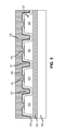
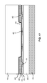
- FIG. 1A is a cross-sectional side view illustration of a bulk LED substrate in accordance with an embodiment of the invention.
- FIG. 1B is a cross-sectional side view illustration of a device wafer including circuitry in accordance with an embodiment of the invention.
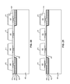
- FIG. 2A is a cross-sectional side view illustration of a patterned conductive contact layer on a bulk LED substrate in accordance with an embodiment of the invention.
- FIG. 2B is a cross-sectional side view illustration of a patterned conductive contact layer on a bulk LED substrate in accordance with an embodiment of the invention.
- FIG. 3 is a cross-sectional side view illustration of a device layer patterned to form an array of micro device mesa structures over a handle substrate in accordance with an embodiment of the invention.
- FIG. 4 is a cross-sectional side view illustration of an adhesion promoter layer and a sacrificial layer including an array of openings formed over an array of micro device mesa structures in accordance with an embodiment of the invention.
- FIG. 5 is a cross-sectional side view illustration of a stabilization layer formed over an adhesion promoter layer and a sacrificial layer and within an array of openings included in the sacrificial layer in accordance with an embodiment of the invention.
- FIG. 6 is a cross-sectional side view illustration of bringing together a carrier substrate having raised spacers and micro device mesa structures formed on a handle substrate in accordance with an embodiment of the invention.
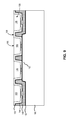
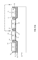
- FIGS. 7A and 7B illustrate example placements of raised spacers on example carrier substrates in accordance with embodiments of the invention.
- FIG. 8 is a cross-sectional side view illustration of a carrier substrate having raised spacers bonded to micro device mesa structures in accordance with an embodiment of the invention.
- FIG. 9 is a cross-sectional side view illustration of the removal of an epitaxial growth layer and a portion of a device layer in accordance with an embodiment of the invention.
- FIGS. 10A and 10B are cross-sectional side view illustrations of patterned conductive contacts formed over an array of laterally separate micro devices in accordance with an embodiment of the invention.
- FIG. 11A is a cross-sectional side view illustration of an array of micro devices formed on an array of stabilization posts after removal of a sacrificial layer in accordance with an embodiment of the invention.
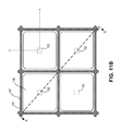
- FIGS. 11B and 11C are schematic top view illustrations of example stabilization post locations relative to a group of micro devices in accordance with an embodiment of the invention.
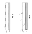
- FIG. 12 is a cross-sectional side view illustration of a bulk LED substrate in accordance with an embodiment of the invention.
- FIG. 13 is a cross-sectional side view illustration of a patterned conductive contact layer on a bulk LED substrate in accordance with an embodiment of the invention.
- FIG. 14 is a cross-sectional side view illustration of an adhesion promoter layer and a sacrificial layer including an array of openings formed over an array of conductive contacts in accordance with an embodiment of the invention.
- FIG. 15 is a cross-sectional side view illustration of a stabilization layer formed over an adhesion promoter layer and a sacrificial layer and within an array of openings in the sacrificial layer in accordance with an embodiment of the invention.
- FIG. 16 is a cross-sectional side view illustration of bringing together a carrier substrate having raised spacers and a stabilization layer formed over a micro device layer in accordance with an embodiment of the invention.
- FIG. 17 is a cross-sectional side view illustration of a carrier substrate having raised spacers bonded to a stabilization layer formed over a micro device layer in accordance with an embodiment of the invention.
- FIG. 18 is a cross-sectional side view illustration of the removal of a substrate in accordance with an embodiment of the invention.
- FIG. 19 is a cross-sectional side view illustration of a device layer patterned to form an array of micro devices over an array of stabilization posts in accordance with an embodiment of the invention.
- FIG. 20 is a cross-sectional side view illustrations of patterned conductive contacts formed over an array of micro devices in accordance with an embodiment of the invention.
- FIG. 21 is a cross-sectional side view illustration of an array of micro devices formed on an array of stabilization posts after removal of a sacrificial layer in accordance with an embodiment of the invention
- FIGS. 22A-22E are cross-sectional side view illustrations of an array of electrostatic transfer heads transferring micro devices from a carrier substrate to a receiving substrate in accordance with an embodiment of the invention.
- Embodiments of the present invention describe a method and structure for stabilizing an array of micro devices such as micro light emitting diode (LED) devices and micro chips on a carrier substrate having raised spacers so that they are poised for pick up and transfer to a receiving substrate.
- the receiving substrate may be, but is not limited to, a display substrate, a lighting substrate, a substrate with functional devices such as transistors or integrated circuits (ICs), or a substrate with metal redistribution lines.
- micro LED devices comprising p-n diodes
- embodiments of the invention are not so limited and that certain embodiments may also be applicable to other micro semiconductor devices which are designed in such a way so as to perform a predetermined electronic function (e.g. diode, transistor, integrated circuit) or photonic function (LED, laser).
- a predetermined electronic function e.g. diode, transistor, integrated circuit
- LED photonic function
- Other embodiments of the present invention are described with specific regard to micro devices including circuitry.
- the micro devices may be based on silicon or SOI wafers for logic or memory applications, or based on GaAs wafers for RF communications applications.
- the terms “upon”, “over”, “spanning”, “to”, “between”, and “on” as used herein may refer to a relative position of one layer with respect to other layers.
- One layer “upon”, “over”, “spanning”, or “on” another layer or bonded “to” another layer may be directly in contact with the other layer or may have one or more intervening layers.
- One layer “between” layers may be directly in contact with the layers or may have one or more intervening layers.
- micro device may refer to the descriptive size of certain devices, devices, or structures in accordance with embodiments of the invention.
- micro device specifically includes “micro LED device” and “micro chip”.
- micro devices or structures may refer to the scale of 1 to 100 ⁇ m. However, it is to be appreciated that embodiments of the present invention are not necessarily so limited, and that certain aspects of the embodiments may be applicable to larger, and possibly smaller “micro” device or structure size scales.
- a single micro device in an array of micro devices, and a single electrostatic transfer head in an array of electrostatic transfer heads both have a maximum dimension, for example length or width, of 1 to 100 ⁇ m.
- the top contact surface of each micro device or electrostatic transfer head has a maximum dimension of 1 to 100 ⁇ m, or more specifically 3 to 20 ⁇ m.
- a pitch of an array of micro devices, and a corresponding array of electrostatic transfer heads is (1 to 100 ⁇ m) by (1 to 100 ⁇ m), for example a 20 ⁇ m by 20 ⁇ m pitch or 5 ⁇ m by 5 ⁇ m pitch.
- the mass transfer of an array of pre-fabricated micro devices with an array of transfer heads is described.
- the pre-fabricated micro devices may have a specific functionality such as, but not limited to, an LED for light-emission, silicon IC for logic and memory, and gallium arsenide (GaAs) circuits for radio frequency (RF) communications.
- arrays of micro LED devices which are poised for pick up are described as having a 20 ⁇ m by 20 ⁇ m pitch, or 5 ⁇ m by 5 ⁇ m pitch.
- a 6 inch substrate can accommodate approximately 165 million micro LED devices with a 10 ⁇ m by 10 ⁇ m pitch, or approximately 660 million micro LED devices with a 5 ⁇ m by 5 ⁇ m pitch.
- a transfer tool including an array of transfer heads matching an integer multiple of the pitch of the corresponding array of micro LED devices can be used to pick up and transfer the array of micro LED devices to a receiving substrate.
- a 1 cm by 1 cm array of micro device transfer heads can pick up and transfer more than 100,000 micro devices, with larger arrays of micro device transfer heads being capable of transferring more micro devices.
- embodiments of the invention describe a structure for stabilizing an array of micro devices such as micro light emitting diode (LED) devices on a carrier substrate having raised spacers so that they are poised for pick up and transfer to a receiving substrate.
- an array of micro devices are held in place on an array of stabilization posts on a carrier substrate having raised spacers.
- the stabilization posts are formed of an adhesive bonding material. In this manner, the array of stabilization posts may retain the array of micro devices in place on a carrier substrate while also providing a structure from which the array of micro devices are readily picked up.
- the adhesive bonding material includes a thermoset material such as, but not limited to, benzocyclobutene (BCB) or epoxy.
- thermoset material may be associated with 10% or less volume shrinkage during curing, or more particularly about 6% or less volume shrinkage during curing. In this manner low volume shrinkage during curing of the adhesive bonding material may not cause delamination between the array of stabilization posts and the array of micro devices, and may allow for uniform adhesion between the array stabilization posts and the array of micro devices supported by the array of stabilization posts.
- a carrier substrate includes raised spacers to increase the planarity of the micro devices that are poised for pick up. It has been observed that the thickness of an adhesive bond layer between two wafers bonded using a conventional adhesive bonding fixture can be non-uniform across the area between the two bonded wafers, despite the use of alignment marks when aligning the two wafers, starting with substantially flat wafers and the use of fixture spacers between the two wafers around the circumference of the wafers. In one scenario, it was observed that when bonding an unpatterned GaN device layer of FIG.
- the thickness of the final cured adhesive bonding layer was measured as being in the range between 1.5-9 ⁇ m across the carrier substrate. It is believed that the resultant non-uniformity in thickness of the adhesive bonding material (referred to as a stabilization layer in this disclosure below) may be attributed to factors such as particulate contamination, wafer bowing, and local stresses within the wafers. For example, wafer bowing of a sapphire growth substrate supporting an epitaxially grown GaN device layer may be from 50-100 ⁇ m in some instances.
- the thickness variation profile of the BCB adhesive bonding material was found to be translated to the GaN device layer surface profiles. Since the micro devices that are formed from the device layer and the transfer heads that transfer the micro devices in accordance with embodiments of the invention may be of the “micro” scale, increasing the planarity of the micro devices with respect to each other and with respect to their carrier substrate may increase the yield of successful transfers of the micro devices from their carrier substrate to a target substrate.
- the raised spacers included in the carrier substrate can extend through the stabilization layer to a more solid structure (e.g. an oxide sacrificial layer) which results in a more uniform thickness of the stabilization layer.
- the micro devices With the raised spacers causing a more uniform thickness in the stabilization layer, the micro devices also have a more planar relationship to each other as they more closely conform to the carrier substrate rather than following a curvature of a bowed handle substrate. As a result, the micro devices have an improved planar positioning across the carrier substrate and the height variation of the top surfaces of the micro devices is reduced, promoting a more consistent pick-up location of the micro devices for successful transfer by the electrostatic transfer heads. Furthermore, the raised spacers can be sized to control the thickness of the stabilization layer to be close to a desired dimension.
- the array of micro devices are formed in a one-sided process sequence in which a device layer is etched to form an array of micro device mesa structures prior to applying a stabilization layer (the stabilization layer having the adhesive bonding material that forms the stabilization posts).
- the array of micro devices are formed in a two-sided process in which a device layer is patterned into micro devices after bonding to a stabilization layer that form the stabilization posts.
- Suitability of a one-sided process or two-sided process may depend upon the system requirement, and materials being used. For example, where the micro devices are micro LED devices, the devices layers may be formed from different materials selected for different emission spectra.
- a blue-emitting or green-emitting micro LED device may be formed of a GaN (5.18 ⁇ lattice constant) based material grown on a sapphire substrate (4.76 ⁇ lattice constant), resulting in a lattice mismatch of approximately 0.42 ⁇ .
- a red-emitting micro LED device may be formed of a GaP (5.45 ⁇ lattice constant) based material grown on a GaAs substrate (5.65 ⁇ lattice constant), resulting in a lattice mismatch of approximately 0.2 ⁇ .
- An increased amount of lattice mismatch between a device layer grown on a growth substrate may result in a greater amount of stress in the device layer.
- a blue-emitting or green-emitting device layer may have a greater amount of intrinsic stress than a red-emitting device layer.
- a one-sided process sequence is performed in order to reduce the amount of shifting between the micro devices and stabilization posts by forming micro device mesa structures on stabilization posts prior to removing the growth substrate.
- the lattice mismatch is less than or equal to 0.2 ⁇
- stress in the device layer may be low enough that it is not an overriding concern and a two-sided process may be more efficient for fabricating the micro devices.
- the two-sided process allows for accurate alignment of the stabilization posts and bottom contacts of the micro devices.
- embodiments of the invention utilize transfer heads and head arrays which operate in accordance with principles of electrostatic grippers, using the attraction of opposite charges to pick up micro devices.
- a pull-in voltage is applied to a transfer head in order to generate a grip pressure on a micro device and pick up the micro device.
- the minimum amount pick up pressure required to pick up a micro device from a stabilization post can be determined by the adhesion strength between the adhesive bonding material from which the stabilization posts are formed and the micro device (or any intermediate layer), as well as the contact area between the top surface of the stabilization post and the micro device.
- adhesion strength which must be overcome to pick up a micro device is related to the minimum pick up pressure generated by a transfer head as provided in equation (1):
- P 1 is the minimum grip pressure required to be generated by a transfer head
- a 1 is the contact area between a transfer head contact surface and micro device contact surface
- a 2 is the contact area on a top surface of a stabilization post
- P 2 is the adhesion strength on the top surface of a stabilization post.
- a grip pressure of greater than 1 atmosphere is generated by a transfer head.
- each transfer head may generate a grip pressure of 2 atmospheres or greater, or even 20 atmospheres or greater without shorting due to dielectric breakdown of the transfer heads. Due to the smaller area, a higher pressure is realized at the top surface of the corresponding stabilization post than the grip pressure generate by a transfer head.
- a bonding layer is placed between each micro device and stabilization post in order to aid in bonding each micro device to a receiving substrate.
- a variety of different bonding layers with different melting temperatures are compatible with embodiments of the invention. For example, heat may or may not be applied to the transfer head assembly, carrier substrate, and/or receiving substrate during the pick up, transfer, and bonding operations.
- the bonding layer may be a comparatively higher melting temperature material such as gold.
- the bonding layer is a comparatively lower melting temperature material such as indium.
- the transfer head assembly may be maintained at an elevated temperature during the pick up and transfer operations in order to assist bonding to the receiving substrate without thermal cycling of the transfer head assembly.
- the bonding layer is gold, and the bonding layer is not liquefied during the pick up or transfer operations. In one embodiment the bonding layer is indium, and the bonding layer is liquefied during the pick up and transfer operations. In such an embodiment, the bonding layer may be partially picked up and transferred to the receiving substrate.
- the bonding layer is formed of a material characterized by a low tensile strength.
- indium is characterized by a tensile strength of approximately 4 MPa which can be less than or near the adhesion strength between a gold/BCB bonding interface of 10 MPa or less, and which is significantly lower than an exemplary 30 MPa adhesion strength between a gold/BCB bonding interface (determined with stud pull test) when treated with adhesion promoter AP3000, an organosilane compound in 1-methoxy-2-propoanol available from The Dow Chemical Company.
- the bonding layer is cleaved during the pick up operation due to the lower tensile strength, and a phase change is not created during the pick up operation. Though, a phase change may still be created in the portion of the bonding layer which is picked up with the micro device during placement of the micro device onto a receiving substrate to aid in bonding of the micro device to the receiving substrate.
- embodiments of the invention describe a manner of forming an array of micro devices which are poised for pick up in which conductive contact layers can be formed on top and bottom surfaces of the micro devices, and annealed to provide ohmic contacts.
- the stabilization layer is formed of a material which is capable of withstanding the associated deposition and annealing temperatures.
- a conductive contact may require annealing at temperatures between 200° C. to 350° C. to form an ohmic contact with the micro device.
- embodiments of the invention may be utilized to form arrays of micro LED devices based upon a variety of different semiconductor compositions for emitting various different visible wavelengths.
- micro LED growth substrates including active devices layers formed of different materials for emitting different wavelengths e.g. red, green, and blue wavelengths
- exemplary processing sequences are described for using a carrier substrate with raised spacers to fabricate an array of micro devices on an array of stabilization posts.
- exemplary processing sequences are described for fabricating an array of micro LED devices and an array of micro chips on an array of stabilization posts.
- FIG. 1A is an example cross-sectional side view illustration of a bulk LED substrate 100 in accordance with an embodiment of the invention.
- bulk LED substrate 100 includes a growth substrate 102 , an epitaxial growth layer 103 , and a device layer 105 .
- growth substrate 102 is sapphire and may be approximately 500 ⁇ m thick.
- Using a sapphire growth substrate may correspond with manufacturing blue emitting LED devices (e.g. 450-495 nm wavelength) or green emitting LED devices (e.g. 495-570 nm wavelength).
- Epitaxial growth layer 103 may be grown on growth substrate 102 using known epitaxial growth techniques. Epitaxial growth layer 103 may be grown on growth substrate 102 at a relatively high temperature to facilitate gliding out dislocations in the layer. In an embodiment, epitaxial growth layer 103 is a gallium nitride (GaN) based material.
- GaN gallium nitride
- Device layer 105 may be formed on epitaxial growth layer 103 , as shown in FIG. 1A .
- the growth substrate 102 is approximately 200 ⁇ m thick.
- the epitaxial growth layer 103 may be any suitable thickness such as between 300 ⁇ -5 ⁇ m.
- device layer 105 includes layers for forming LED devices.
- a zoomed-in view of an example device layer 105 illustrates one or more quantum well layers 110 between doped semiconductor layer 108 (e.g. n-doped) and doped semiconductor layer 112 (e.g. p-doped), although the doping of layers 108 and 112 may be reversed.
- doped semiconductor layer 108 is formed of GaN and is approximately 0.1 ⁇ m to 3 ⁇ m thick.
- the one or more quantum well layers 110 may have a thickness of approximately 0.5 ⁇ m.
- doped semiconductor layer 112 is formed of GaN, and is approximately 0.1 ⁇ m to 2 ⁇ m thick.
- FIG. 1B is a cross-sectional side view illustration of a device wafer 180 including circuitry in accordance with an embodiment of the invention.
- the device wafer 180 may be formed of a variety of materials depending upon the desired function.
- the device wafer 180 is a silicon wafer, or silicon-on-insulator (SOI) wafer for logic or memory.
- the device wafer 180 is a gallium arsenide (GaAs) wafer for radio frequency (RF) communications.
- GaAs gallium arsenide
- RF radio frequency
- the device wafer 180 includes an active device layer 185 , optional buried oxide layer 184 , and base substrate 182 .
- the active device layer 185 may include working circuitry to control one or more LED devices.
- back-end processing may be performed within the active device layer 185 .
- the active device layer 185 includes an active silicon layer 187 including devices such as transistors, metal build-up layers 188 including interconnects 189 , bonding pads 190 , and passivation 192 .
- both the growth substrate 102 and base substrate 182 can alternatively be referred to more generically as a “handle” substrate so as to not preclude the processing sequence on a growth substrate 102 from being applied to the processing sequence on a base substrate 182 .
- FIG. 2A is a cross-sectional side view illustration of a patterned conductive contact layer on bulk LED substrate 100 in accordance with an embodiment of the invention.
- a conductive contact layer may be formed over device layer 105 using a suitable technique such as sputtering or electron beam physical deposition followed by etching or liftoff to form the array of conductive contacts 120 .
- the array of conductive contacts 120 have a thickness of approximately 0.1 ⁇ m-2 ⁇ m, and may include a plurality of different layers.
- a conductive contact 120 may include an electrode layer 121 for ohmic contact, a mirror layer 122 , an adhesion/barrier layer 123 , a diffusion barrier layer 124 , and a bonding layer 125 .
- electrode layer 121 may make ohmic contact to a p-doped semiconductor layer 112 , and may be formed of a high work-function metal such as nickel.
- a minor layer 122 such as silver is formed over the electrode layer 121 to reflect the transmission of the visible wavelength.
- titanium is used as an adhesion/barrier layer 123
- platinum is used as a diffusion barrier 124 to bonding layer 125 .
- Bonding layer 125 may be formed of a variety of materials which can be chosen for bonding to the receiving substrate and/or to achieve the requisite tensile strength or adhesion or surface tension with the stabilization posts (yet to be formed).
- the substrate stack can be annealed to form an ohmic contact.
- a p-side ohmic contact may be formed by annealing the substrate stack at 510° C. for 10 minutes.
- bonding layer 125 is formed of a conductive material (both pure metals and alloys) which can diffuse with a metal forming a contact pad on a receiving substrate (e.g. gold, indium, or tin contact pad) and has a liquidus temperature above 200° C. such as tin (231.9° C.) or bismuth (271.4° C.), or a liquidus temperature above 300° C. such as gold (1064° C.) or silver (962° C.).
- bonding layer 125 such as gold may be selected for its poor adhesion with the adhesive bonding material used to form the stabilization posts.
- noble metals such as gold are known to achieve poor adhesion with BCB.
- the anneal (e.g. 510° C. for 10 minutes) can be performed after the formation of the patterned conductive contact layer 120 , including bonding layer 125 .
- the bonding layer 125 may be formed after annealing.
- FIG. 2B is a cross-sectional side view illustration of a patterned conductive contact layer on a bulk LED substrate 100 in accordance with an embodiment of the invention.
- the embodiment illustrated in FIG. 2B may be particularly useful where bonding layer 125 is formed of a material with a liquidus temperature below the annealing temperature of the p-side ohmic contact, though the embodiment illustrated in FIG. 2B is not limited to such and may be used where the bonding layer 125 is formed of a material with a liquidus temperature above the annealing temperature of the p-side ohmic contact.
- electrode layer 121 and minor layer 122 may be formed similarly as described with regard to FIG. 2A .
- adhesion/barrier layer 123 and diffusion barrier 124 may be formed similarly as described with regard to FIG. 2A with one difference being that the layers 123 and 124 may optionally wrap around the sidewalls of the layers 121 and 122 .
- the substrate stack can be annealed to form an ohmic contact.
- a p-side ohmic contact may be formed by annealing the substrate stack at 510° C. for 10 minutes.
- the bonding layer 125 may be formed.
- the bonding layer 125 has a smaller width than for layers 121 - 124 .
- bonding layer 125 has a liquidus temperature or melting temperature of approximately 350° C. or lower, or more specifically of approximately 200° C. or lower. At such temperatures the bonding layer may undergo a phase change without substantially affecting the other components of the micro LED device.
- the resultant bonding layer may be electrically conductive.
- the bonding layer 125 may be a solder material, such as an indium, bismuth, or tin based solder, including pure metals and metal alloys. In a particular embodiment, the bonding layer 125 is indium.
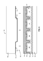
- FIG. 3 is a cross-sectional side view illustration of device layer 105 patterned to form an array of micro device mesa structures 127 over a handle substrate that includes growth substrate 102 and epitaxial growth layer 103 in accordance with an embodiment of the invention.
- Etching of layers 108 , 110 , and 112 of device layer 105 may be accomplished using suitable etch chemistries for the particular materials.
- n-doped semiconductor layer 108 , quantum well layer(s) 110 , and p-doped layer 112 may be dry etched in one operation with a BCl 3 and Cl 2 chemistry.
- FIG. 3 is a cross-sectional side view illustration of device layer 105 patterned to form an array of micro device mesa structures 127 over a handle substrate that includes growth substrate 102 and epitaxial growth layer 103 in accordance with an embodiment of the invention.
- Etching of layers 108 , 110 , and 112 of device layer 105 may be accomplished using suitable etch chemistries for the particular materials.
- device layer 105 may not be etched completely through which leaves unremoved portions 129 of device layer 105 that connect the micro device mesa structures 127 .
- the etching of device layer 105 is stopped in n-doped semiconductor layer 108 (which may be n-doped GaN).
- a height of the micro device mesa structures 127 (not including the thickness of the unremoved portions 129 may correspond substantially to the height of the laterally separate micro devices to be formed.
- the device layer 105 may alternatively be completely etched through. For example, where the bulk LED substrate 100 is replaced with a device wafer 180 in the processing sequence, etching may stop on the buried oxide layer 184 .
- FIG. 4 is a cross-sectional side view illustration of an adhesion promoter layer 144 and a sacrificial layer 135 including an array of openings 133 formed over the array of micro device mesa structures 127 in accordance with an embodiment of the invention.
- sacrificial layer 135 is between approximately 0.5 and 2 microns thick.
- sacrificial layer 135 is formed of an oxide (e.g. SiO 2 ) or nitride (e.g. SiN x ), though other materials may be used which can be selectively removed with respect to the other layers.
- sacrificial layer 135 is deposited by sputtering, low temperature plasma enhanced chemical vapor deposition (PECVD), or electron beam evaporation to create a low quality layer, which may be more easily removed than a higher quality layer deposited by other methods such as atomic layer deposition (ALD) or high temperature PECVD.
- PECVD low temperature plasma enhanced chemical vapor deposition
- ALD atomic layer deposition
- PECVD high temperature PECVD
- an adhesion promoter layer 144 may optionally be formed in order to increase adhesion of the stabilization layer 145 (not yet formed) to the sacrificial layer 135 .
- a thickness of 100-300 angstroms may be sufficient to increase adhesion.
- Specific metals that have good adhesion to both the sacrificial layer 135 and a BCB stabilization layer include, but are not limited to, titanium and chromium.
- sputtered or evaporated titanium or chromium can achieve an adhesion strength (stud pull) of greater than 40 MPa with BCB.
- the sacrificial layer 135 is patterned to form an array of openings 133 over the array of conductive contacts 120 . If adhesion promoter layer 144 is present, it can also be patterned to form the array of openings 133 , exposing the array of conductive contacts 120 as illustrated in FIG. 4 .
- a fluorinated chemistry e.g. HF vapor, or CF 4 or SF 6 plasma
- FIG. 4 illustrates an optional adhesion promoter layer 144 being patterned with the sacrificial layer 135 to form openings.
- an adhesion promoter layer 144 may optionally be formed after patterning sacrificial layer 135 to form openings 133 .
- the adhesion promoter layer may be formed within the openings 133 and on conductive contacts 120 . This may have the effect of increasing the pull force required to subsequently separate conductive contacts 120 and stabilization layer 145 (yet to be formed).
- the structure including patterned sacrificial layer 135 is treated with an adhesion promoter such as AP3000, available from The Dow Chemical Company, in the case of a BCB stabilization layer 145 in order to condition the underlying structure.
- AP3000 for example, can be spin coated onto the underlying structure, and soft baked (e.g. 100° C.) or spun dry to remove the solvents prior to applying the stabilization layer 145 over the patterned sacrificial layer.
- openings 133 in the sacrificial layer 135 correspond to the height, and length and width (area) of the stabilization posts to be formed, and resultantly the adhesion strength that must be overcome to pick up the array of micro devices (e.g. micro LED devices) poised for pick up on the array of stabilization posts.
- openings 133 are formed using lithographic techniques and have a length and width of approximately 1 ⁇ m by 1 ⁇ m, though the openings may be larger or smaller so long as the openings have a width (or area) that is less than the width (or area) of the conductive contacts 120 and/or micro LED devices.
- the height, length and width of the openings 131 between the sacrificial layer 135 formed along sidewalls between the micro device mesa structures 127 will correspond to the height, length and width of the stabilization cavity sidewalls to be formed. Accordingly, increasing the thickness of the sacrificial layer 135 and the space separating adjacent micro device mesa structures 127 will have the effect of decreasing the size of the stabilization cavity sidewalls.
- FIG. 5 is a cross-sectional side view illustration of a stabilization layer 145 formed over adhesion promoter layer 144 and sacrificial layer 135 and within an array of openings 133 included in sacrificial layer 135 in accordance with an embodiment of the invention.
- Stabilization layer 145 may be formed of an adhesive bonding material.
- the adhesive bonding material may be a thermosetting material such as benzocyclobutene (BCB) or epoxy.
- the thermosetting material may be associated with 10% or less volume shrinkage during curing, or more particularly about 6% or less volume shrinkage during curing so as to not delaminate from the conductive contacts 120 on the micro device mesa structures 127 .
- stabilization layer 145 is spin coated or spray coated over the patterned sacrificial layer 135 , though other application techniques may be used.
- the structure may be spun at 5,000 RPM to form the stabilization layer 145 at a thickness of 2 ⁇ m ⁇ 0.5 ⁇ m.
- the structure may be pre-baked at between 120 and 200° C. for 10-30 minutes to remove solvents, resulting in a b-staged layer.
- the stabilization layer 145 is thicker than the height of openings 131 (when present) between micro device mesa structures 127 .
- the thickness of the stabilization layer filling openings 133 will become stabilization posts 152
- the thickness of the stabilization layer filling openings 131 will become stabilization cavity sidewalls 147
- the remainder of the thickness of the stabilization layer 145 over the filled openings 131 , 133 can function to adhesively bond the bulk LED substrate 100 to a carrier substrate.
- FIG. 6 is a cross-sectional side view illustration of bringing together (bonding) a carrier substrate 160 having raised spacers 163 and micro device mesa structures 127 formed on a handle substrate in accordance with an embodiment of the invention.
- Carrier substrate 160 has a back side 164 opposite a spacer side 165 .
- Spacer side 165 includes raised spacers 163 extending away from a spacer-side surface 167 of carrier substrate 160 .
- raised spacers 163 are made from the same material (e.g. silicon) as the carrier substrate 160 .
- Raised spacers 163 may be formed using a subtractive process that etches or mills away part of carrier substrate 160 to make raised spacers 163 .
- Raised spacers 163 could also be of a different material than carrier substrate 160 and added to carrier substrate 160 in an additive process. In one example, oxide is added to carrier substrate 160 to form raised spacers 163 on carrier substrate 160 .
- FIGS. 7A and 7B illustrate example placements of raised spacers 163 on example carrier substrates 160 in accordance with embodiments of the invention.
- FIGS. 7A and 7B show a top view looking down on spacer side 165 of carrier substrates 160 .
- Carrier substrate 160 may be approximately six inches in diameter and be made of silicon.
- FIG. 7A shows raised spacers 163 arranged in a pattern following concentric circles.
- FIG. 7B shows raised spacers 163 arranged in a rectangular grid pattern.
- the height of raised spacers 163 is 80-90% of a thickness of a stabilization layer 145 .
- raised spacers 163 that are taller than stabilization layer 163 can cause air gaps to form between stabilization layer 145 and carrier substrate 160 , yet raised spacers 163 that are too short may make it difficult to force excess stabilization layer 145 away.
- raised spacers 163 are illustrated as circular, raised spacers 163 may also have a rectangular shape, when viewed from a view point that looks down on spacer side 165 , such as in FIGS. 7A and 7B .
- carrier substrate 160 is bonded to the micro device mesa structures 127 via the adhesion properties of stabilization layer 145 .
- 1,100 kg of force is applied for between two and three hours to bond carrier substrate 160 to the micro device mesa structures. Bonding may take place at approximately 200° C.
- an adhesion promoter layer 162 can be applied to the carrier substrate 160 prior to bonding the bulk LED substrate 100 to the carrier substrate 160 similarly as described above with regard to adhesion promoter layer 144 .
- an adhesion promoter such as AP3000 may be applied to the surface of the carrier substrate 160 or adhesion promoter layer 162 .
- stabilization layer 145 can be formed on carrier substrate 160 prior to bonding the carrier substrate 160 to the handle substrate.
- the structure including the patterned sacrificial layer 135 and micro device mesa structures 127 can be embossed into an a-staged or b-staged stabilization layer 145 formed on the carrier substrate 160 .
- stabilization layer 145 may be thermally cured, or cured with application of UV energy.
- stabilization layer 145 is a-staged or b-staged prior to bonding the carrier substrate to the handle substrate, and is cured at a temperature or temperature profile ranging between 150° C. and 300° C.
- curing temperatures should not exceed approximately 350° C., which represents the temperature at which BCB begins to degrade.
- a bonding layer 125 material characterized by a liquidus temperature (e.g.
- a BCB stabilization layer 145 can be achieved in approximately 1 hour or less at a curing temperature between 250° C. and 300° C.
- Other bonding layer 125 materials such as Sn (231.9° C.) may require between 10-100 hours to fully cure at temperatures between 200° C. and the 231.9° C. liquidus temperature.
- a BCB stabilization layer 145 may only be partially cured (e.g. 70% or greater). In such an embodiment the BCB stabilization layer 145 may be cured at a temperature between 150° C. and the liquidus temperature of the bonding layer (e.g. 156.7° C. for indium) for approximately 100 hours to achieve at least a 70% cure.
- the stabilization layer 145 may be cured to a sufficient curing percentage (e.g. 70% or greater for BCB) at which point the stabilization layer 145 will no longer reflow. Moreover, it has been observed that such partially cured (e.g. 70% or greater) BCB stabilization layer 145 may possess sufficient adhesion strengths with the carrier substrate 160 and patterned sacrificial layer 135 (or any intermediate layer(s)).
- a sufficient curing percentage e.g. 70% or greater for BCB
- FIG. 8 is a cross-sectional side view illustration of carrier substrate 160 bonded to the micro device mesa structures 127 formed over the handle substrate in accordance with an embodiment of the invention.
- raised spacer 163 of carrier substrate 160 has been brought to rest upon sacrificial layer 135 .
- raised spacers 163 extend into stabilization layer 145 , meeting at least a subset of stabilization posts 152 in the structure illustrated in FIG. 8 .
- adhesion promoter layer 144 and 162 may be disposed between sacrificial layer 135 and carrier substrate 160 , but in other embodiments, raised spacer 163 of carrier substrate 160 may contact sacrificial layer 135 .
- the planar alignment of micro devices 128 and uniformity in thickness of the stabilization layer 145 across the carrier substrate 160 may improve.
- the improvement may manifest in comparison to having micro devices 128 and associated structure “float” atop stabilization layer 145 without any solid underpinning to carrier substrate 160 .
- the micro devices and the transfer heads that transfer the micro devices may be of on the ⁇ m scale, increasing the planarity of the micro devices with respect to each other and with respect to their carrier substrate 160 may increase the yield of successful transfers of the micro devices from their carrier substrate to a target substrate. Due to the improved planar positioning of the micro devices, the pick-up location of the micro devices becomes better defined for successful transfer by the electrostatic transfer heads.
- FIG. 8 also shows that growth substrate 102 has been removed.
- growth substrate 102 is sapphire
- laser lift off (LLO) may be used to remove the sapphire. Removal may be accomplished by other techniques such as grinding and etching, depending upon the material selection of the growth substrate 102 .
- FIG. 9 is a cross-sectional side view illustration of the removal of an epitaxial growth layer 103 and a portion of device layer 105 in accordance with an embodiment of the invention.
- the removal of epitaxial growth layer 103 and a portion of device layer 105 may be accomplished using one or more of Chemical-Mechanical-Polishing (CMP), dry polishing, or dry etch.
- CMP Chemical-Mechanical-Polishing
- FIG. 9 illustrates that that unremoved portions 129 of device layer 105 that connected the micro device mesa structures 127 ( FIG. 7 ) are removed in FIG. 9 , which leaves laterally separated micro devices 128 .
- removing unremoved portions 129 of device layer 105 includes thinning the array of micro device mesa structures 127 so that an exposed top surface 109 of each of the laterally separate micro devices 128 are below an exposed top surface 139 of patterned sacrificial layer 135 .
- a portion of the doped semiconductor layer 108 adjacent the epitaxial growth layer may also function as a “buffer”.
- epitaxial growth layer 103 may or may not be doped, while semiconductor layer 108 is n-doped. It may be preferred to remove the epitaxial growth layer 103 using any suitable technique such as wet or dry etching, or CMP, followed by a timed etch of the remainder of the doped semiconductor layer 108 resulting in the structure illustrated in FIG. 9 .
- the thickness of the laterally separate micro devices 128 is largely determined by the etching operation illustrated in FIG. 3 for the formation of the micro device mesa structures 127 , combined with the timed etch or etch stop detection of the etching operation illustrated in FIG. 9 .
- raised spacer 163 is shown “covering” an area that is two micro devices 128 wide. However, in one embodiment, raised spacer 163 covers an area that is five micro devices 128 wide, resulting in a total coverage of approximately 25 micro devices 128 . In one embodiment raised spacers 163 are circular having a diameter of 60-100 ⁇ m. The raised spacers are interspersed on the carrier substrate to cover only a small percentage (e.g. ⁇ 5%) of the micro devices.
- FIGS. 10A-10B are cross-sectional side view illustrations of patterned conductive contacts 175 formed over the array of laterally separated micro device 128 in accordance with an embodiment of the invention.
- FIGS. 10A and 10B are substantially similar, with a difference being the arrangement of layers within conductive contacts 120 .
- FIG. 10A corresponds with the conductive contacts 120 illustrated in FIG. 2A while FIG. 10B corresponds with the conductive contacts 120 illustrated in FIG. 2B .
- a conductive contact layer is formed over micro devices 128 and sacrificial layer 135 .
- the conductive contact layer may be formed of a variety of conductive materials including metals, conductive oxides, and conductive polymers.
- conductive contacts are formed of a metal or metal alloy.
- the conductive contact layer is formed using a suitable technique such as sputtering or electron beam physical deposition.
- the conductive contact layer may include BeAu metal alloy, or a metal stack of Au/GeAuNi/Au layers.
- the conductive contact layer can also be a combination of one or more metal layers and a conductive oxide.
- the substrate stack is annealed to generate an ohmic contact between the conductive contact layer and the device layer of micro devices 128 .
- the annealing temperature may be below approximately 350° C., at which point BCB degrades. In an embodiment, annealing is performed between 200° C. and 350° C., or more particularly at approximately 320° C. for approximately 10 minutes.
- the conductive contact layer is deposited, it can be patterned and etched to form conductive contacts 175 , which may be n-metal conductive contacts.
- each micro device may have a minimum width (e.g. along the top surface 109 ) of 4.5 ⁇ m, and a separation between adjacent micro devices of 0.5 ⁇ m. It is to be appreciated that a pitch of 5 microns is exemplary, and that embodiments of the invention encompass any pitch of 1 to 100 ⁇ m as well as larger, and possibly smaller pitches.
- FIGS. 10A and 10B illustrate a structure having a stabilization layer 145 that includes an array of stabilization cavities and an array of stabilization posts 152 .
- Each stabilization cavity in the array includes sidewalls 147 (which may be coated with adhesion promoter layer 144 ) of stabilization layer 145 that surround stabilization posts 152 .
- the bottom surface 107 (having dimension D1) of each micro device 128 is wider that the corresponding stabilization post 152 that is directly under the micro device 128 .
- sacrificial layer 135 spans along side surfaces 106 of micro devices 128 .
- stabilization posts 152 extend through a thickness of sacrificial layer 135 and the stabilization cavity sidewalls 147 of the stabilization layer 145 are taller than the stabilization posts 152 . However, in some embodiments, stabilization posts 152 are taller than the stabilization cavity sidewalls 147 .
- FIG. 11A is a cross-sectional side view illustration of an array of micro devices 128 formed on array of stabilization posts 152 after removal of sacrificial layer 135 in accordance with an embodiment of the invention.
- sacrificial layer 135 is removed resulting in an open space 177 between each micro device 128 and stabilization layer 145 .
- open space 177 includes the open space below each micro device 128 and stabilization layer 145 as well as the open space between each micro device 128 and stabilization cavity sidewalls 147 of stabilization layer 145 .
- a suitable etching chemistry such as HF vapor, CF 4 , or SF 6 plasma may be used to etch the SiO 2 or SiN x of sacrificial layer 135 .
- the raised spacers 163 may be removed along with sacrificial layer 135 if the etching chemistry for both sacrificial layer 135 and raised spacers 163 (formed of oxide) are similar.
- the array of micro devices 128 on the array of stabilization posts 152 are supported only by the array of stabilization posts 152 . At this point, the array of micro devices 128 are poised for pick up transferring to a target or receiving substrate.
- the stabilization cavity sidewalls 147 may be advantageously positioned to contain the shifted micro device 128 within the stabilization cavity. Therefore, even when a micro device 128 loses adherence to a stabilization post 152 , it may still be poised for pick up because it is still positioned within an acceptable tolerance (defined by the stabilization cavity) to be transferred to a receiving substrate.
- FIGS. 11B-11C are schematic top view illustrations of example stabilization post 152 locations relative to a group of micro devices 128 in accordance with an embodiment of the invention.
- the cross-sectional side view of FIG. 11A is illustrated along line A-A in FIGS. 11B and 11C .
- FIG. 11B shows an embodiment where stabilization posts 152 are centered in the x-y directions relative to a top view illustration of micro devices 128 .
- FIG. 11B also shows how stabilization cavity sidewalls 147 can function to contain micro devices 128 , if a micro device 128 loses adhesion to a stabilization post 152 .
- FIG. 11C is substantially similar to FIG. 11B except that stabilization posts 153 have replaced stabilization posts 152 .
- Stabilization posts 153 differ from stabilization posts 152 in that they are not centered in the x-y direction relative to a top view illustration of the micro devices 128 .
- positions of stabilization posts other than the illustrated positions of stabilization posts 152 and 153 are possible.
- the off-centered stabilization posts 153 may provide for the creation of a moment when the array of transfer heads contact the array of micro devices in which the micro devices tilt slightly as a result of the applied downward pressure from the array of transfer heads. This slight tilting may aid in overcoming the adhesion strength between the stabilization posts 153 and the array of micro devices 128 .
- such assistance in overcoming the adhesion strength may potentially allow for picking up the array of micro devices with a lower grip pressure. Consequently, this may allow for operation of the array of transfer heads at a lower voltage, and impose less stringent dielectric strength requirements in the dielectric layer covering each transfer head required to achieve the electrostatic grip pressure.
- FIGS. 1A-11C have described a “one-sided process” for the production of micro devices, such as blue-emitting and green-emitting micro LEDs.
- the device layer used to fabricate blue-emitting and green-emitting LEDs may be under a higher amount of stress than other device layers grown on growth substrates with less lattice mismatch.
- the one-sided process may reduce shifting between the micro devices 128 and the stabilization posts 152 when removing the growth substrate 102 since the patterning of micro device mesa structures 127 relieves stress within the device layer 105 prior to removing the growth substrate 102 , which may produce high quality micro devices that are also positioned within an acceptable tolerance.
- a “two-sided” process may be used to form micro devices, such as red-emitting micro LEDs when intrinsic stress within a device layer is not an overriding factor.
- FIGS. 12-21 illustrate one example of a two-sided process suitable for fabricating red-emitting micro LEDs and LEDs of other color emissions as well.
- FIG. 12 is a cross-sectional side view illustration of a bulk LED substrate 400 in accordance with an embodiment of the invention.
- bulk LED substrate 400 includes a substrate 402 and a device layer 405 .
- substrate 402 is gallium arsenide (GaAs) and may be approximately 200-700 ⁇ m thick.
- Device layer 405 may be formed on substrate 402 , as shown in FIG. 12 .
- device layer 405 includes layers for forming LED devices.
- a zoomed-in view of an example device layer 405 illustrates one or more quantum well layers 110 between doped semiconductor layer 108 (e.g. n-doped) and doped semiconductor layer 112 (e.g.
- micro chips may be similarly manufactured by substituting device layer 405 with the active device layer 185 illustrated in FIG. 1B .
- FIG. 13 is a cross-sectional side view illustration of a patterned conductive contact layer on bulk LED substrate 400 in accordance with an embodiment of the invention.
- a conductive contact layer may be formed over device layer 405 using a suitable technique such as sputtering or electron beam physical deposition followed by etching or liftoff to form the array of conductive contacts 420 .
- Conductive contacts may be formed and have the same properties as described in the different embodiments described in association with FIGS. 2A and 2B .
- FIG. 14 is a cross-sectional side view illustration of an adhesion promoter layer 444 and a sacrificial layer 435 including an array of openings 433 formed over an array of conductive contacts 420 in accordance with an embodiment of the invention.
- sacrificial layer 435 is between approximately 0.5 and 2 microns thick.
- sacrificial layer 435 is formed of an oxide (e.g. SiO 2 ) or nitride (e.g. SiN x ), though other materials may be used which can be selectively removed with respect to the other layers.
- sacrificial layer 435 is deposited by sputtering, low temperature PECVD, or electron beam evaporation to create a low quality layer, which may be more easily removed than a higher quality layer deposited by other methods such as ALD or high temperature PECVD.
- an adhesion promoter layer 444 may optionally be formed in order to increase adhesion of the stabilization layer 445 (not yet formed) to the sacrificial layer 435 .
- a thickness of 100-300 angstroms may be sufficient to increase adhesion.
- the sacrificial layer 435 is patterned to form an array of openings 433 over the array of conductive contacts 420 . If adhesion layer 444 is present, it can also be patterned to form the array of openings 433 , exposing the array of conductive contacts 420 as illustrated in FIG. 14 .
- a fluorinated chemistry e.g. HF vapor, or CF 4 or SF 6 plasma
- FIG. 14 illustrates an optional adhesion promoter layer 444 being patterned with the sacrificial layer 435 to form openings 433 .
- an adhesion promoter layer 444 may optionally be formed after patterning sacrificial layer 435 to form openings 433 .
- the adhesion promoter layer may be formed within the openings 433 and on conductive contacts 420 . This may have the effect of increasing the pull force required to subsequently separate conductive contacts 420 and stabilization layer 445 (yet to be formed).
- the structure including patterned sacrificial layer 135 is treated with an adhesion promoter such as AP3000, available from The Dow Chemical Company, in the case of a BCB stabilization layer 445 in order to condition the underlying structure.
- AP3000 for example, can be spin coated onto the underlying structure, and soft baked (e.g. 100° C.) or spun dry to remove the solvents prior to applying the stabilization layer 445 over the patterned sacrificial layer.
- openings 433 in the sacrificial layer 435 correspond to the height, and length and width (area) of the stabilization posts 452 to be formed, and resultantly the adhesion strength that must be overcome to pick up the array of micro devices (e.g. micro LED devices) poised for pick up on the array of stabilization posts.
- openings 433 are formed using lithographic techniques and have a length and width of approximately 1 ⁇ m by 1 ⁇ m, though the openings may be larger or smaller so long as the openings have a width (or area) that is less than the width (or area) of the conductive contacts 420 and/or micro LED devices.
- FIG. 15 is a cross-sectional side view illustration of a stabilization layer 445 formed over adhesion promoter layer 444 and sacrificial layer 435 and within an array of openings 433 included in sacrificial layer 435 in accordance with an embodiment of the invention.
- Stabilization layer 445 may be formed of an adhesive bonding material.
- the adhesive bonding material may be a thermosetting material such as benzocyclobutene (BCB) or epoxy.
- stabilization layer 445 is spin coated or spray coated over the patterned sacrificial layer 435 , though other application techniques may be used. Following application of the stabilization layer 445 , the structure may be pre-baked to remove solvents, resulting in a b-staged layer. The thickness of the stabilization layer 445 filling openings 433 will become stabilization posts 452 and the remainder of the thickness of the stabilization layer 445 can function to adhesively bond the bulk LED substrate 400 to carrier substrate 460 , shown in FIG. 16 .
- the “two-sided process” described with regard to FIGS. 12-21 allows for accurate alignment of the stabilization posts 452 and conductive contacts 420 . This may be attributed to the sacrificial layer 435 being planar during patterning to form openings 433 , which allows for accurate and uniform photoresist development. Accordingly, alignment error can be reduced using the “two-sided process” where shifting of the device layer 405 after removal of the growth substrate 402 is not an overriding factor.
- FIG. 16 is a cross-sectional side view illustration of bringing together carrier substrate 460 having raised spacers 463 and stabilization layer 445 formed over a micro device layer 405 in accordance with an embodiment of the invention.
- Carrier substrate 460 has a back side 464 opposite a spacer side 465 .
- Spacer side 465 includes raised spacers 463 extending away from a spacer-side surface 467 of carrier substrate 460 .
- raised spacers 463 are made from the same material (e.g. silicon) as the carrier substrate 460 .
- Raised spacers 463 may be formed using a subtractive process that etches or mills away part of carrier substrate 460 to make raised spacers 463 .
- Raised spacers 463 could also be of a different material than carrier substrate 460 and added to carrier substrate 460 in an additive process.
- oxide is added to carrier substrate 460 to form raised spacers 463 on carrier substrate 460 .
- Carrier substrate 460 may have the same or similar placements of raised spacers 463 as described in reference to carrier substrate 160 and raised spacers 163 , shown in FIGS. 7A and 7B .
- carrier substrate 460 is bonded to the underlying structure (which includes bulk LED substrate 400 , conduction contacts 420 and sacrificial layer 435 ) via the adhesion properties of stabilization layer 445 .
- an adhesion promoter layer 462 can be applied to the carrier substrate 460 prior to bonding the bulk LED substrate 400 to the carrier substrate 460 similarly as described above with regard to adhesion promoter layer 144 .
- stabilization layer 445 may be thermally cured, or cured with application of UV energy, as described in connection with stabilization layer 145 .
- FIG. 17 is a cross-sectional side view illustration of carrier substrate 460 having raised spacers 463 bonded to a stabilization layer 445 formed over micro device layer 405 in accordance with an embodiment of the invention.
- raised spacer 463 of carrier substrate 460 has been brought to rest upon sacrificial layer 435 .
- raised spacers 463 extend into stabilization layer 445 , meeting at least a subset of stabilization posts 452 in the structure illustrated in FIG. 17 .
- adhesion promoter layer 444 and 462 may be disposed between sacrificial layer 435 and carrier substrate 460 , but in other embodiments, raised spacer 463 of carrier substrate 460 may contact sacrificial layer 435 .
- FIG. 18 is a cross-sectional side view illustration of the removal of substrate 402 in accordance with an embodiment of the invention.
- wet etch chemistry may be used to remove substrate 402 .
- a NH 4 OH and H 2 O 2 chemistry is used to wet etch a substrate 402 that is of GaAs. Removal may be accomplished by other techniques such as grinding or CMP, depending upon the material selection of substrate 402 .
- FIG. 19 is a cross-sectional side view illustration of device layer 405 patterned to form an array of micro devices 428 over an array of stabilization posts 452 in accordance with an embodiment of the invention.
- Etching of layers 108 , 110 , and 112 of device layer 405 may be accomplished using suitable etch chemistries for the particular materials. For example, n-doped semiconductor layer 108 , quantum well layer(s) 110 , and p-doped layer 112 may be dry etched in one operation with a BCl 3 and Cl 2 chemistry. After the appropriate layers of device layer 405 are etched, an array of micro devices 428 remains.
- raised spacer 463 is shown “covering” an area that is two micro devices 428 wide. However, in one embodiment, raised spacer 463 covers an area that is five micro devices 428 wide, resulting in a total coverage of approximately 25 micro devices 428 . In one embodiment raised spacers 463 are circular, having a diameter of 60-100 ⁇ m.
- FIG. 20 is a cross-sectional side view illustrations of patterned conductive contacts 475 formed over the array of micro devices 428 in accordance with an embodiment of the invention.
- Conductive contacts 475 may be formed by electron beam physical deposition or by another suitable method.
- Conductive contact 475 may be formed of a variety of conductive materials including metals, conductive oxides, and conductive polymers.
- conductive contacts 475 are formed of a metal or metal alloy.
- Conductive contacts 475 may include conductive contact layers that include BeAu metal alloy, or a metal stack of Au/GeAuNi/Au layers.
- the conductive contact layer can also be a combination of one or more metal layers and a conductive oxide.
- conductive contacts 475 are n-metal conductive contacts.
- each micro device 428 may have a minimum width of 4.5 ⁇ m, and a separation between adjacent micro devices of 0.5 ⁇ m. It is to be appreciated that a pitch of 5 microns is exemplary, and that embodiments of the invention encompass any pitch of 1 to 100 ⁇ m as well as larger, and possibly smaller pitches. Also in FIG. 20 , a bottom surface of each micro device 428 is wider that the corresponding stabilization post 452 that is directly under the micro device 428 . In the illustrated embodiments, stabilization posts 452 extend into a thickness of sacrificial layer 435 .
- FIG. 21 is a cross-sectional side view illustration of the array of micro devices 428 formed on an array of stabilization posts 452 after removal of a sacrificial layer 435 in accordance with an embodiment of the invention.
- a suitable etching chemistry such as HF vapor, CF 4 , or SF 6 plasma may be used to etch if sacrificial layer 435 includes SiO 2 or SiN x , for example.
- raised spacers 463 are formed of an oxide material
- the raised spacers 463 may be removed along with sacrificial layer 435 if the etching chemistry for both sacrificial layer 435 and raised spacers 463 (formed of oxide) are similar.
- the array of micro devices 428 remain on the array of stabilization posts 452 and are supported only by the array of stabilization posts 152 . At this point, the array of micro devices 428 are poised for pick up transferring to a target or receiving substrate.
- FIGS. 22A-22E are cross-sectional side view illustrations of an array of electrostatic transfer heads 204 transferring micro devices 128 from a carrier substrate 160 to a receiving substrate 300 in accordance with an embodiment of the invention. Although the transfer process illustrated in FIGS. 22A-22E is shown using the structure of FIG. 11A , the transfer process could also be performed using the structure from FIG. 21 .
- FIG. 22A is a cross-sectional side view illustration of an array of micro device transfer heads 204 supported by substrate 200 and positioned over an array of micro devices 128 stabilized on stabilization posts 152 of stabilization layer 145 on carrier substrate 160 .
- the array of micro devices 128 are then contacted with the array of transfer heads 204 as illustrated in FIG. 22B .
- the pitch of the array of transfer heads 204 is an integer multiple of the pitch of the array of micro devices 128 .
- a voltage is applied to the array of transfer heads 204 .
- the voltage may be applied from the working circuitry within a transfer head assembly 206 in electrical connection with the array of transfer heads through vias 207 .
- the array of micro devices 128 is then picked up with the array of transfer heads 204 as illustrated in FIG.
- the array of micro devices 128 is then placed in contact with contact pads 302 (e.g. gold, indium, or tin) on a receiving substrate 300 , as illustrated in FIG. 22D .
- the array of micro devices 128 is then released onto contact pads 302 on receiving substrate 300 as illustrated in FIG. 22E .
- the receiving substrate may be, but is not limited to, a display substrate, a lighting substrate, a substrate with functional devices such as transistors or ICs, or a substrate with metal redistribution lines.
- heat may be applied to the carrier substrate, transfer head assembly, or receiving substrate during the pickup, transfer, and bonding operations.
- heat can be applied through the transfer head assembly during the pick up and transfer operations, in which the heat may or may not liquefy the micro device bonding layers 125 .
- the transfer head assembly may additionally apply heat during the bonding operation on the receiving substrate that may or may not liquefy one of the bonding layers on the micro device or receiving substrate to cause diffusion between the bonding layers.
- the operation of applying the voltage to create a grip pressure on the array of micro devices can be performed in various orders.
- the voltage can be applied prior to contacting the array of micro devices with the array of transfer heads, while contacting the micro devices with the array of transfer heads, or after contacting the micro devices with the array of transfer heads.
- the voltage may also be applied prior to, while, or after applying heat to the bonding layers.
- an alternating voltage may be applied across a the pair of electrodes in each transfer head 204 so that at a particular point in time when a negative voltage is applied to one electrode, a positive voltage is applied to the other electrode in the pair, and vice versa to create the pickup pressure.
- Releasing the array of micro devices from the transfer heads 204 may be accomplished with a varied of methods including turning off the voltage sources, lower the voltage across the pair of silicon electrodes, changing a waveform of the AC voltage, and grounding the voltage sources.
- the method of pickup up and transferring the array of micro devices from a carrier substrate to a receiving substrate described with regard to FIGS. 22A-22E is applicable in contexts where the micro devices are micro LEDs or other examples of micro devices described herein.
Abstract
Description
- 1. Field
- The present invention relates to micro devices. More particularly embodiments of the present invention relate to the stabilization of micro devices on a carrier substrate.
- 2. Background Information
- Commercial manufacturing and packaging of micro devices often becomes more challenging as the scale of the micro devices decreases. Some examples of micro devices include radio frequency (RF) microelectromechanical systems (MEMS) microswitches, light-emitting diode (LED) display systems, and MEMS or quartz-based oscillators.
- During fabrication of active devices, it is common to include bonding together two wafers or substrates. For example, a growth substrate may be bonded with a carrier substrate to position the device structure on a different wafer or substrate in order to perform processing operations on an alternate side of the micro device structure. The growth substrate may also be bonded with a carrier substrate because the carrier substrate is better suited to continue on in the fabrication process.
- To bond one substrate/wafer to another, an adhesive bonding material may be applied as an adhesive layer between the two substrates. A wafer bonding fixture may be used to facilitate the process. The wafer bonding fixture may assist on exerting a controlled amount of pressure on the two wafers to encourage a close and uniform bonding of the two wafers. In some instances, the wafers to be bonded have alignment marks to promote a uniform bonding distance between the two wafers. In addition, the wafer bonding fixture may include fixture spacers positioned around the circumference of the two wafers in order to determine a thickness of the adhesive bonding material, and consequently, the spacing between the two wafers.
- A structure and method of forming an array of micro devices which are poised for pick up are disclosed. In an embodiment, a structure include a stabilization layer including an array of stabilization posts. In an embodiment, the stabilization layer is formed of a thermoset material such as epoxy or benzocyclobutene (BCB) which is associated with 10% or less volume shrinkage during curing. An array of micro devices are formed over the array of stabilization posts. The structure includes a carrier substrate that includes raised spacers extending from a spacer-side surface of the carrier substrate. The raised spacers extend into the stabilization layer to meet a subset of the stabilization posts in the array of stabilization posts. In an embodiment the array of stabilization posts are separated by a pitch of 1 μm to 100 μm, or more specifically 1 μm to 10 μm. The array of micro devices may be micro LED devices, and may be designed to emit a specific wavelength such as a red, green, or blue light. In an embodiment, each micro LED device includes a device layer formed of a p-doped semiconductor layer, one or more quantum well layers over the p-doped semiconductor layer, and an n-doped semiconductor layer. For example, where the micro LED device is designed to emit a green or blue light, the p-doped layer may comprise GaN and the n-doped layer may also comprise GaN.
- In one embodiment, a device layer is patterned to form an array of micro device mesa structures over a handle substrate. A patterned sacrificial layer including an array of openings is then formed over the array of micro device mesa structures. A stabilization layer can then be formed over the patterned sacrificial layer and within the array of openings. The stabilization layer is bonded to a spacer side of a carrier substrate. The spacer side of the carrier substrate includes raised spacers extending from a spacer-side surface. An adhesion promoter layer may be formed between the carrier substrate and the stabilization layer to increase adhesion.
- In one embodiment, a patterned sacrificial layer including an array of openings is formed over a device layer. A stabilization layer is then formed over the patterned sacrificial layer and within the array of openings. The stabilization layer may be bonded to a spacer side of a carrier substrate. The spacer side of the carrier substrate includes raised spacers extending from a spacer-side surface. After bonding the stabilization layer to the spacer side of the carrier substrate, the device layer may be patterned to form the array of micro devices.
-
FIG. 1A is a cross-sectional side view illustration of a bulk LED substrate in accordance with an embodiment of the invention. -
FIG. 1B is a cross-sectional side view illustration of a device wafer including circuitry in accordance with an embodiment of the invention. -
FIG. 2A is a cross-sectional side view illustration of a patterned conductive contact layer on a bulk LED substrate in accordance with an embodiment of the invention. -
FIG. 2B is a cross-sectional side view illustration of a patterned conductive contact layer on a bulk LED substrate in accordance with an embodiment of the invention. -
FIG. 3 is a cross-sectional side view illustration of a device layer patterned to form an array of micro device mesa structures over a handle substrate in accordance with an embodiment of the invention. -
FIG. 4 is a cross-sectional side view illustration of an adhesion promoter layer and a sacrificial layer including an array of openings formed over an array of micro device mesa structures in accordance with an embodiment of the invention. -
FIG. 5 is a cross-sectional side view illustration of a stabilization layer formed over an adhesion promoter layer and a sacrificial layer and within an array of openings included in the sacrificial layer in accordance with an embodiment of the invention. -
FIG. 6 is a cross-sectional side view illustration of bringing together a carrier substrate having raised spacers and micro device mesa structures formed on a handle substrate in accordance with an embodiment of the invention. -
FIGS. 7A and 7B illustrate example placements of raised spacers on example carrier substrates in accordance with embodiments of the invention. -
FIG. 8 is a cross-sectional side view illustration of a carrier substrate having raised spacers bonded to micro device mesa structures in accordance with an embodiment of the invention. -
FIG. 9 is a cross-sectional side view illustration of the removal of an epitaxial growth layer and a portion of a device layer in accordance with an embodiment of the invention. -
FIGS. 10A and 10B are cross-sectional side view illustrations of patterned conductive contacts formed over an array of laterally separate micro devices in accordance with an embodiment of the invention. -
FIG. 11A is a cross-sectional side view illustration of an array of micro devices formed on an array of stabilization posts after removal of a sacrificial layer in accordance with an embodiment of the invention. -
FIGS. 11B and 11C are schematic top view illustrations of example stabilization post locations relative to a group of micro devices in accordance with an embodiment of the invention. -
FIG. 12 is a cross-sectional side view illustration of a bulk LED substrate in accordance with an embodiment of the invention. -
FIG. 13 is a cross-sectional side view illustration of a patterned conductive contact layer on a bulk LED substrate in accordance with an embodiment of the invention. -
FIG. 14 is a cross-sectional side view illustration of an adhesion promoter layer and a sacrificial layer including an array of openings formed over an array of conductive contacts in accordance with an embodiment of the invention. -
FIG. 15 is a cross-sectional side view illustration of a stabilization layer formed over an adhesion promoter layer and a sacrificial layer and within an array of openings in the sacrificial layer in accordance with an embodiment of the invention. -
FIG. 16 is a cross-sectional side view illustration of bringing together a carrier substrate having raised spacers and a stabilization layer formed over a micro device layer in accordance with an embodiment of the invention. -
FIG. 17 is a cross-sectional side view illustration of a carrier substrate having raised spacers bonded to a stabilization layer formed over a micro device layer in accordance with an embodiment of the invention. -
FIG. 18 is a cross-sectional side view illustration of the removal of a substrate in accordance with an embodiment of the invention. -
FIG. 19 is a cross-sectional side view illustration of a device layer patterned to form an array of micro devices over an array of stabilization posts in accordance with an embodiment of the invention. -
FIG. 20 is a cross-sectional side view illustrations of patterned conductive contacts formed over an array of micro devices in accordance with an embodiment of the invention. -
FIG. 21 is a cross-sectional side view illustration of an array of micro devices formed on an array of stabilization posts after removal of a sacrificial layer in accordance with an embodiment of the invention -
FIGS. 22A-22E are cross-sectional side view illustrations of an array of electrostatic transfer heads transferring micro devices from a carrier substrate to a receiving substrate in accordance with an embodiment of the invention. - Embodiments of the present invention describe a method and structure for stabilizing an array of micro devices such as micro light emitting diode (LED) devices and micro chips on a carrier substrate having raised spacers so that they are poised for pick up and transfer to a receiving substrate. For example, the receiving substrate may be, but is not limited to, a display substrate, a lighting substrate, a substrate with functional devices such as transistors or integrated circuits (ICs), or a substrate with metal redistribution lines. While embodiments of some of the present invention are described with specific regard to micro LED devices comprising p-n diodes, it is to be appreciated that embodiments of the invention are not so limited and that certain embodiments may also be applicable to other micro semiconductor devices which are designed in such a way so as to perform a predetermined electronic function (e.g. diode, transistor, integrated circuit) or photonic function (LED, laser). Other embodiments of the present invention are described with specific regard to micro devices including circuitry. For example, the micro devices may be based on silicon or SOI wafers for logic or memory applications, or based on GaAs wafers for RF communications applications.
- In various embodiments, description is made with reference to figures. However, certain embodiments may be practiced without one or more of these specific details, or in combination with other known methods and configurations. In the following description, numerous specific details are set forth, such as specific configurations, dimensions and processes, etc., in order to provide a thorough understanding of the present invention. In other instances, well-known semiconductor processes and manufacturing techniques have not been described in particular detail in order to not unnecessarily obscure the present invention. Reference throughout this specification to “one embodiment,” “an embodiment” or the like means that a particular feature, structure, configuration, or characteristic described in connection with the embodiment is included in at least one embodiment of the invention. Thus, the appearances of the phrase “in one embodiment,” “an embodiment” or the like in various places throughout this specification are not necessarily referring to the same embodiment of the invention. Furthermore, the particular features, structures, configurations, or characteristics may be combined in any suitable manner in one or more embodiments.
- The terms “upon”, “over”, “spanning”, “to”, “between”, and “on” as used herein may refer to a relative position of one layer with respect to other layers. One layer “upon”, “over”, “spanning”, or “on” another layer or bonded “to” another layer may be directly in contact with the other layer or may have one or more intervening layers. One layer “between” layers may be directly in contact with the layers or may have one or more intervening layers.
- The terms “micro” device, “micro” LED device, or “micro” chip as used herein may refer to the descriptive size of certain devices, devices, or structures in accordance with embodiments of the invention. As used herein the term “micro device” specifically includes “micro LED device” and “micro chip”. As used herein, the terms “micro” devices or structures may refer to the scale of 1 to 100 μm. However, it is to be appreciated that embodiments of the present invention are not necessarily so limited, and that certain aspects of the embodiments may be applicable to larger, and possibly smaller “micro” device or structure size scales. In an embodiment, a single micro device in an array of micro devices, and a single electrostatic transfer head in an array of electrostatic transfer heads both have a maximum dimension, for example length or width, of 1 to 100 μm. In an embodiment, the top contact surface of each micro device or electrostatic transfer head has a maximum dimension of 1 to 100 μm, or more specifically 3 to 20 μm. In an embodiment, a pitch of an array of micro devices, and a corresponding array of electrostatic transfer heads is (1 to 100 μm) by (1 to 100 μm), for example a 20 μm by 20 μm pitch or 5 μm by 5 μm pitch.
- In the following embodiments, the mass transfer of an array of pre-fabricated micro devices with an array of transfer heads is described. For example, the pre-fabricated micro devices may have a specific functionality such as, but not limited to, an LED for light-emission, silicon IC for logic and memory, and gallium arsenide (GaAs) circuits for radio frequency (RF) communications. In some embodiments, arrays of micro LED devices which are poised for pick up are described as having a 20 μm by 20 μm pitch, or 5 μm by 5 μm pitch. At these densities, a 6 inch substrate, for example, can accommodate approximately 165 million micro LED devices with a 10 μm by 10 μm pitch, or approximately 660 million micro LED devices with a 5 μm by 5 μm pitch. A transfer tool including an array of transfer heads matching an integer multiple of the pitch of the corresponding array of micro LED devices can be used to pick up and transfer the array of micro LED devices to a receiving substrate. In this manner, it is possible to integrate and assemble micro LED devices into heterogeneously integrated systems, including substrates of any size ranging from micro displays to large area displays, and at high transfer rates. For example, a 1 cm by 1 cm array of micro device transfer heads can pick up and transfer more than 100,000 micro devices, with larger arrays of micro device transfer heads being capable of transferring more micro devices.
- In one aspect, embodiments of the invention describe a structure for stabilizing an array of micro devices such as micro light emitting diode (LED) devices on a carrier substrate having raised spacers so that they are poised for pick up and transfer to a receiving substrate. In an embodiment, an array of micro devices are held in place on an array of stabilization posts on a carrier substrate having raised spacers. In an embodiment, the stabilization posts are formed of an adhesive bonding material. In this manner, the array of stabilization posts may retain the array of micro devices in place on a carrier substrate while also providing a structure from which the array of micro devices are readily picked up. In an embodiment, the adhesive bonding material includes a thermoset material such as, but not limited to, benzocyclobutene (BCB) or epoxy. In an embodiment, the thermoset material may be associated with 10% or less volume shrinkage during curing, or more particularly about 6% or less volume shrinkage during curing. In this manner low volume shrinkage during curing of the adhesive bonding material may not cause delamination between the array of stabilization posts and the array of micro devices, and may allow for uniform adhesion between the array stabilization posts and the array of micro devices supported by the array of stabilization posts.
- In one aspect of embodiments of the invention, a carrier substrate includes raised spacers to increase the planarity of the micro devices that are poised for pick up. It has been observed that the thickness of an adhesive bond layer between two wafers bonded using a conventional adhesive bonding fixture can be non-uniform across the area between the two bonded wafers, despite the use of alignment marks when aligning the two wafers, starting with substantially flat wafers and the use of fixture spacers between the two wafers around the circumference of the wafers. In one scenario, it was observed that when bonding an unpatterned GaN device layer of
FIG. 1A described below to a silicon carrier substrate with an BCB adhesive bonding layer of approximately 2 μm thickness, the thickness of the final cured adhesive bonding layer was measured as being in the range between 1.5-9 μm across the carrier substrate. It is believed that the resultant non-uniformity in thickness of the adhesive bonding material (referred to as a stabilization layer in this disclosure below) may be attributed to factors such as particulate contamination, wafer bowing, and local stresses within the wafers. For example, wafer bowing of a sapphire growth substrate supporting an epitaxially grown GaN device layer may be from 50-100 μm in some instances. While the thickness of the GaN device layer remained constant across the substrate, the thickness variation profile of the BCB adhesive bonding material was found to be translated to the GaN device layer surface profiles. Since the micro devices that are formed from the device layer and the transfer heads that transfer the micro devices in accordance with embodiments of the invention may be of the “micro” scale, increasing the planarity of the micro devices with respect to each other and with respect to their carrier substrate may increase the yield of successful transfers of the micro devices from their carrier substrate to a target substrate. During an adhesive bonding operation of the stabilization layer and the carrier substrate, the raised spacers included in the carrier substrate can extend through the stabilization layer to a more solid structure (e.g. an oxide sacrificial layer) which results in a more uniform thickness of the stabilization layer. With the raised spacers causing a more uniform thickness in the stabilization layer, the micro devices also have a more planar relationship to each other as they more closely conform to the carrier substrate rather than following a curvature of a bowed handle substrate. As a result, the micro devices have an improved planar positioning across the carrier substrate and the height variation of the top surfaces of the micro devices is reduced, promoting a more consistent pick-up location of the micro devices for successful transfer by the electrostatic transfer heads. Furthermore, the raised spacers can be sized to control the thickness of the stabilization layer to be close to a desired dimension. - In one aspect of embodiments of the invention, the array of micro devices are formed in a one-sided process sequence in which a device layer is etched to form an array of micro device mesa structures prior to applying a stabilization layer (the stabilization layer having the adhesive bonding material that forms the stabilization posts). In one aspect of embodiments of the invention, the array of micro devices are formed in a two-sided process in which a device layer is patterned into micro devices after bonding to a stabilization layer that form the stabilization posts. Suitability of a one-sided process or two-sided process may depend upon the system requirement, and materials being used. For example, where the micro devices are micro LED devices, the devices layers may be formed from different materials selected for different emission spectra. By way of example, a blue-emitting or green-emitting micro LED device may be formed of a GaN (5.18 Å lattice constant) based material grown on a sapphire substrate (4.76 Å lattice constant), resulting in a lattice mismatch of approximately 0.42 Å. By way of comparison, a red-emitting micro LED device may be formed of a GaP (5.45 Å lattice constant) based material grown on a GaAs substrate (5.65 Å lattice constant), resulting in a lattice mismatch of approximately 0.2 Å. An increased amount of lattice mismatch between a device layer grown on a growth substrate may result in a greater amount of stress in the device layer. In the above exemplary growth systems, a blue-emitting or green-emitting device layer may have a greater amount of intrinsic stress than a red-emitting device layer.
- It has been observed that when fabricating devices at the “micro” scale, stress in a device layer may cause the device layer to shift laterally upon removal of a growth substrate that the device layer is grown upon. This stress may potentially cause misalignment between the array of micro devices that are formed over an array of stabilization posts. In accordance with embodiments of the invention, and in particular when lattice mismatch between the device layer and growth substrate is greater than approximately 0.2 Å, a one-sided process sequence is performed in order to reduce the amount of shifting between the micro devices and stabilization posts by forming micro device mesa structures on stabilization posts prior to removing the growth substrate. However, when the lattice mismatch is less than or equal to 0.2 Å, stress in the device layer may be low enough that it is not an overriding concern and a two-sided process may be more efficient for fabricating the micro devices. As will become more apparent in the following description, the two-sided process allows for accurate alignment of the stabilization posts and bottom contacts of the micro devices.
- Without being limited to a particular theory, embodiments of the invention utilize transfer heads and head arrays which operate in accordance with principles of electrostatic grippers, using the attraction of opposite charges to pick up micro devices. In accordance with embodiments of the present invention, a pull-in voltage is applied to a transfer head in order to generate a grip pressure on a micro device and pick up the micro device. In accordance with embodiments of the invention, the minimum amount pick up pressure required to pick up a micro device from a stabilization post can be determined by the adhesion strength between the adhesive bonding material from which the stabilization posts are formed and the micro device (or any intermediate layer), as well as the contact area between the top surface of the stabilization post and the micro device. For example, adhesion strength which must be overcome to pick up a micro device is related to the minimum pick up pressure generated by a transfer head as provided in equation (1):
-
P 1 A 1 =P 2 A 2 (1) - where P1 is the minimum grip pressure required to be generated by a transfer head, A1 is the contact area between a transfer head contact surface and micro device contact surface, A2 is the contact area on a top surface of a stabilization post, and P2 is the adhesion strength on the top surface of a stabilization post. In an embodiment, a grip pressure of greater than 1 atmosphere is generated by a transfer head. For example, each transfer head may generate a grip pressure of 2 atmospheres or greater, or even 20 atmospheres or greater without shorting due to dielectric breakdown of the transfer heads. Due to the smaller area, a higher pressure is realized at the top surface of the corresponding stabilization post than the grip pressure generate by a transfer head. In an embodiment, a bonding layer is placed between each micro device and stabilization post in order to aid in bonding each micro device to a receiving substrate. A variety of different bonding layers with different melting temperatures are compatible with embodiments of the invention. For example, heat may or may not be applied to the transfer head assembly, carrier substrate, and/or receiving substrate during the pick up, transfer, and bonding operations. In some embodiments, the bonding layer may be a comparatively higher melting temperature material such as gold. In some embodiments the bonding layer is a comparatively lower melting temperature material such as indium. In some embodiments, the transfer head assembly may be maintained at an elevated temperature during the pick up and transfer operations in order to assist bonding to the receiving substrate without thermal cycling of the transfer head assembly. In one embodiment, the bonding layer is gold, and the bonding layer is not liquefied during the pick up or transfer operations. In one embodiment the bonding layer is indium, and the bonding layer is liquefied during the pick up and transfer operations. In such an embodiment, the bonding layer may be partially picked up and transferred to the receiving substrate.
- In another embodiment, the bonding layer is formed of a material characterized by a low tensile strength. For example, indium is characterized by a tensile strength of approximately 4 MPa which can be less than or near the adhesion strength between a gold/BCB bonding interface of 10 MPa or less, and which is significantly lower than an exemplary 30 MPa adhesion strength between a gold/BCB bonding interface (determined with stud pull test) when treated with adhesion promoter AP3000, an organosilane compound in 1-methoxy-2-propoanol available from The Dow Chemical Company. In an embodiment, the bonding layer is cleaved during the pick up operation due to the lower tensile strength, and a phase change is not created during the pick up operation. Though, a phase change may still be created in the portion of the bonding layer which is picked up with the micro device during placement of the micro device onto a receiving substrate to aid in bonding of the micro device to the receiving substrate.
- In another aspect, embodiments of the invention describe a manner of forming an array of micro devices which are poised for pick up in which conductive contact layers can be formed on top and bottom surfaces of the micro devices, and annealed to provide ohmic contacts. Where a conductive contact is formed on a top surface of a micro device, the stabilization layer is formed of a material which is capable of withstanding the associated deposition and annealing temperatures. For example, a conductive contact may require annealing at temperatures between 200° C. to 350° C. to form an ohmic contact with the micro device. In this manner, embodiments of the invention may be utilized to form arrays of micro LED devices based upon a variety of different semiconductor compositions for emitting various different visible wavelengths. For example, micro LED growth substrates including active devices layers formed of different materials for emitting different wavelengths (e.g. red, green, and blue wavelengths) can all be processed within the general sequence of operations of the embodiments.
- In the following description exemplary processing sequences are described for using a carrier substrate with raised spacers to fabricate an array of micro devices on an array of stabilization posts. Specifically, exemplary processing sequences are described for fabricating an array of micro LED devices and an array of micro chips on an array of stabilization posts. Where possible, similar features are illustrated with similar annotations in the figures and following description.
-
FIG. 1A is an example cross-sectional side view illustration of abulk LED substrate 100 in accordance with an embodiment of the invention. In the illustrated embodiment,bulk LED substrate 100 includes agrowth substrate 102, anepitaxial growth layer 103, and adevice layer 105. In an embodiment,growth substrate 102 is sapphire and may be approximately 500 μm thick. Using a sapphire growth substrate may correspond with manufacturing blue emitting LED devices (e.g. 450-495 nm wavelength) or green emitting LED devices (e.g. 495-570 nm wavelength). It is to be appreciated, that while the specific embodiments illustrated and described in the following description may be directed to formation of green or blue emitting LED devices, the following sequences and descriptions are also applicable to the formation of LED devices that emit wavelengths other than blue and green.Epitaxial growth layer 103 may be grown ongrowth substrate 102 using known epitaxial growth techniques.Epitaxial growth layer 103 may be grown ongrowth substrate 102 at a relatively high temperature to facilitate gliding out dislocations in the layer. In an embodiment,epitaxial growth layer 103 is a gallium nitride (GaN) based material. -
Device layer 105 may be formed onepitaxial growth layer 103, as shown inFIG. 1A . In an embodiment thegrowth substrate 102 is approximately 200 μm thick. Theepitaxial growth layer 103 may be any suitable thickness such as between 300 Å-5 μm. In the illustrated embodiment,device layer 105 includes layers for forming LED devices. InFIG. 1A , a zoomed-in view of anexample device layer 105 illustrates one or more quantum well layers 110 between doped semiconductor layer 108 (e.g. n-doped) and doped semiconductor layer 112 (e.g. p-doped), although the doping oflayers semiconductor layer 108 is formed of GaN and is approximately 0.1 μm to 3 μm thick. The one or more quantum well layers 110 may have a thickness of approximately 0.5 μm. In an embodiment, dopedsemiconductor layer 112 is formed of GaN, and is approximately 0.1 μm to 2 μm thick. -
FIG. 1B is a cross-sectional side view illustration of adevice wafer 180 including circuitry in accordance with an embodiment of the invention. In accordance with embodiments of the invention, thedevice wafer 180 may be formed of a variety of materials depending upon the desired function. For example, in an embodiment, thedevice wafer 180 is a silicon wafer, or silicon-on-insulator (SOI) wafer for logic or memory. In an embodiment, thedevice wafer 180 is a gallium arsenide (GaAs) wafer for radio frequency (RF) communications. These are merely examples, and embodiments of the invention envision are not limited to silicon or GaAs wafers, nor are embodiments limited to logic, memory, or RF communications. - In an embodiment, the
device wafer 180 includes anactive device layer 185, optionalburied oxide layer 184, andbase substrate 182. In the interest of clarity, the following description is made with regard to anSOI device wafer 180, including anactive device layer 185, buriedoxide layer 184, andbase silicon substrate 182, though other types of devices wafers may be used, including bulk semiconductor wafers. In an embodiment, theactive device layer 185 may include working circuitry to control one or more LED devices. In some embodiments, back-end processing may be performed within theactive device layer 185. Accordingly, in an embodiment, theactive device layer 185 includes anactive silicon layer 187 including devices such as transistors, metal build-uplayers 188 includinginterconnects 189,bonding pads 190, andpassivation 192. - In the interest of clarity, the portion of the disclosure associated with
FIGS. 2A-11C is made with regard to the bulk LED substrate ofFIG. 1A . However, it is appreciated that the process sequences in the following description may be used to fabricate other micro devices. For example, micro chips may be similarly manufactured by substitutingbulk LED substrate 100 withdevice wafer 180 and using the same or similar processes as described with reference tobulk LED substrate 100. Accordingly, in the following description, both thegrowth substrate 102 andbase substrate 182 can alternatively be referred to more generically as a “handle” substrate so as to not preclude the processing sequence on agrowth substrate 102 from being applied to the processing sequence on abase substrate 182. -
FIG. 2A is a cross-sectional side view illustration of a patterned conductive contact layer onbulk LED substrate 100 in accordance with an embodiment of the invention. A conductive contact layer may be formed overdevice layer 105 using a suitable technique such as sputtering or electron beam physical deposition followed by etching or liftoff to form the array ofconductive contacts 120. In an embodiment, the array ofconductive contacts 120 have a thickness of approximately 0.1 μm-2 μm, and may include a plurality of different layers. For example, aconductive contact 120 may include anelectrode layer 121 for ohmic contact, amirror layer 122, an adhesion/barrier layer 123, adiffusion barrier layer 124, and abonding layer 125. In an embodiment,electrode layer 121 may make ohmic contact to a p-dopedsemiconductor layer 112, and may be formed of a high work-function metal such as nickel. In an embodiment, aminor layer 122 such as silver is formed over theelectrode layer 121 to reflect the transmission of the visible wavelength. In an embodiment, titanium is used as an adhesion/barrier layer 123, and platinum is used as adiffusion barrier 124 tobonding layer 125.Bonding layer 125 may be formed of a variety of materials which can be chosen for bonding to the receiving substrate and/or to achieve the requisite tensile strength or adhesion or surface tension with the stabilization posts (yet to be formed). Following the formation of layers 121-125, the substrate stack can be annealed to form an ohmic contact. For example, a p-side ohmic contact may be formed by annealing the substrate stack at 510° C. for 10 minutes. - In an embodiment,
bonding layer 125 is formed of a conductive material (both pure metals and alloys) which can diffuse with a metal forming a contact pad on a receiving substrate (e.g. gold, indium, or tin contact pad) and has a liquidus temperature above 200° C. such as tin (231.9° C.) or bismuth (271.4° C.), or a liquidus temperature above 300° C. such as gold (1064° C.) or silver (962° C.). In some embodiments,bonding layer 125 such as gold may be selected for its poor adhesion with the adhesive bonding material used to form the stabilization posts. For example, noble metals such as gold are known to achieve poor adhesion with BCB. In this manner, sufficient adhesion is created to maintain the array of micro LED devices on the stabilization posts during processing and handling, as well as to maintain adjacent micro LED devices in place when another micro LED device is being picked up, yet also not create too much adhesion so that pick up can be achieved with an applied pick up pressure on the transfer head of 20 atmospheres or less, or more particularly 5-10 atmospheres. - In the embodiment illustrated in
FIG. 2A , wherebonding layer 125 has a liquidus temperature above the annealing temperature for forming the p-side ohmic contact, the anneal (e.g. 510° C. for 10 minutes) can be performed after the formation of the patternedconductive contact layer 120, includingbonding layer 125. Wherebonding layer 125 has a liquidus temperature below the annealing temperature for forming the p-side ohmic contact, thebonding layer 125 may be formed after annealing. -
FIG. 2B is a cross-sectional side view illustration of a patterned conductive contact layer on abulk LED substrate 100 in accordance with an embodiment of the invention. The embodiment illustrated inFIG. 2B may be particularly useful wherebonding layer 125 is formed of a material with a liquidus temperature below the annealing temperature of the p-side ohmic contact, though the embodiment illustrated inFIG. 2B is not limited to such and may be used where thebonding layer 125 is formed of a material with a liquidus temperature above the annealing temperature of the p-side ohmic contact. In such embodiments,electrode layer 121 andminor layer 122 may be formed similarly as described with regard toFIG. 2A . Likewise, adhesion/barrier layer 123 anddiffusion barrier 124 may be formed similarly as described with regard toFIG. 2A with one difference being that thelayers layers bonding layer 125 may be formed. In an embodiment, thebonding layer 125 has a smaller width than for layers 121-124. - In an embodiment,
bonding layer 125 has a liquidus temperature or melting temperature of approximately 350° C. or lower, or more specifically of approximately 200° C. or lower. At such temperatures the bonding layer may undergo a phase change without substantially affecting the other components of the micro LED device. In an embodiment, the resultant bonding layer may be electrically conductive. In accordance with some embodiments, thebonding layer 125 may be a solder material, such as an indium, bismuth, or tin based solder, including pure metals and metal alloys. In a particular embodiment, thebonding layer 125 is indium. -
FIG. 3 is a cross-sectional side view illustration ofdevice layer 105 patterned to form an array of microdevice mesa structures 127 over a handle substrate that includesgrowth substrate 102 andepitaxial growth layer 103 in accordance with an embodiment of the invention. Etching oflayers device layer 105 may be accomplished using suitable etch chemistries for the particular materials. For example, n-dopedsemiconductor layer 108, quantum well layer(s) 110, and p-dopedlayer 112 may be dry etched in one operation with a BCl3 and Cl2 chemistry. AsFIG. 3 illustrates,device layer 105 may not be etched completely through which leavesunremoved portions 129 ofdevice layer 105 that connect the microdevice mesa structures 127. In one example, the etching ofdevice layer 105 is stopped in n-doped semiconductor layer 108 (which may be n-doped GaN). A height of the micro device mesa structures 127 (not including the thickness of theunremoved portions 129 may correspond substantially to the height of the laterally separate micro devices to be formed. In accordance with embodiments of the invention, thedevice layer 105 may alternatively be completely etched through. For example, where thebulk LED substrate 100 is replaced with adevice wafer 180 in the processing sequence, etching may stop on the buriedoxide layer 184. -
FIG. 4 is a cross-sectional side view illustration of anadhesion promoter layer 144 and asacrificial layer 135 including an array ofopenings 133 formed over the array of microdevice mesa structures 127 in accordance with an embodiment of the invention. In an embodiment,sacrificial layer 135 is between approximately 0.5 and 2 microns thick. In an embodiment,sacrificial layer 135 is formed of an oxide (e.g. SiO2) or nitride (e.g. SiNx), though other materials may be used which can be selectively removed with respect to the other layers. In an embodiment,sacrificial layer 135 is deposited by sputtering, low temperature plasma enhanced chemical vapor deposition (PECVD), or electron beam evaporation to create a low quality layer, which may be more easily removed than a higher quality layer deposited by other methods such as atomic layer deposition (ALD) or high temperature PECVD. - Still referring to
FIG. 4 , after the formation ofsacrificial layer 135, anadhesion promoter layer 144 may optionally be formed in order to increase adhesion of the stabilization layer 145 (not yet formed) to thesacrificial layer 135. A thickness of 100-300 angstroms may be sufficient to increase adhesion. - Specific metals that have good adhesion to both the
sacrificial layer 135 and a BCB stabilization layer (not yet formed) include, but are not limited to, titanium and chromium. For example, sputtered or evaporated titanium or chromium can achieve an adhesion strength (stud pull) of greater than 40 MPa with BCB. - After forming
sacrificial layer 135, thesacrificial layer 135 is patterned to form an array ofopenings 133 over the array ofconductive contacts 120. Ifadhesion promoter layer 144 is present, it can also be patterned to form the array ofopenings 133, exposing the array ofconductive contacts 120 as illustrated inFIG. 4 . In an example embodiment, a fluorinated chemistry (e.g. HF vapor, or CF4 or SF6 plasma) is used to etch the SiO2 or SiNxsacrificial layer 135.FIG. 4 illustrates an optionaladhesion promoter layer 144 being patterned with thesacrificial layer 135 to form openings. In other embodiments anadhesion promoter layer 144 may optionally be formed after patterningsacrificial layer 135 to formopenings 133. In such embodiments, the adhesion promoter layer may be formed within theopenings 133 and onconductive contacts 120. This may have the effect of increasing the pull force required to subsequently separateconductive contacts 120 and stabilization layer 145 (yet to be formed). In one embodiment, the structure including patternedsacrificial layer 135 is treated with an adhesion promoter such as AP3000, available from The Dow Chemical Company, in the case of aBCB stabilization layer 145 in order to condition the underlying structure. AP3000, for example, can be spin coated onto the underlying structure, and soft baked (e.g. 100° C.) or spun dry to remove the solvents prior to applying thestabilization layer 145 over the patterned sacrificial layer. - As will become more apparent in the following description the height, and length and width of the
openings 133 in thesacrificial layer 135 correspond to the height, and length and width (area) of the stabilization posts to be formed, and resultantly the adhesion strength that must be overcome to pick up the array of micro devices (e.g. micro LED devices) poised for pick up on the array of stabilization posts. In an embodiment,openings 133 are formed using lithographic techniques and have a length and width of approximately 1 μm by 1 μm, though the openings may be larger or smaller so long as the openings have a width (or area) that is less than the width (or area) of theconductive contacts 120 and/or micro LED devices. Furthermore, the height, length and width of theopenings 131 between thesacrificial layer 135 formed along sidewalls between the microdevice mesa structures 127 will correspond to the height, length and width of the stabilization cavity sidewalls to be formed. Accordingly, increasing the thickness of thesacrificial layer 135 and the space separating adjacent microdevice mesa structures 127 will have the effect of decreasing the size of the stabilization cavity sidewalls. -
FIG. 5 is a cross-sectional side view illustration of astabilization layer 145 formed overadhesion promoter layer 144 andsacrificial layer 135 and within an array ofopenings 133 included insacrificial layer 135 in accordance with an embodiment of the invention.Stabilization layer 145 may be formed of an adhesive bonding material. The adhesive bonding material may be a thermosetting material such as benzocyclobutene (BCB) or epoxy. In an embodiment, the thermosetting material may be associated with 10% or less volume shrinkage during curing, or more particularly about 6% or less volume shrinkage during curing so as to not delaminate from theconductive contacts 120 on the microdevice mesa structures 127. - In an embodiment,
stabilization layer 145 is spin coated or spray coated over the patternedsacrificial layer 135, though other application techniques may be used. For spin coating, the structure may be spun at 5,000 RPM to form thestabilization layer 145 at a thickness of 2 μm±0.5 μm. Following application of thestabilization layer 145, the structure may be pre-baked at between 120 and 200° C. for 10-30 minutes to remove solvents, resulting in a b-staged layer. In an embodiment, thestabilization layer 145 is thicker than the height of openings 131 (when present) between microdevice mesa structures 127. In this manner, the thickness of the stabilizationlayer filling openings 133 will become stabilization posts 152, the thickness of the stabilizationlayer filling openings 131 will become stabilization cavity sidewalls 147, and the remainder of the thickness of thestabilization layer 145 over the filledopenings bulk LED substrate 100 to a carrier substrate. -
FIG. 6 is a cross-sectional side view illustration of bringing together (bonding) acarrier substrate 160 having raisedspacers 163 and microdevice mesa structures 127 formed on a handle substrate in accordance with an embodiment of the invention.Carrier substrate 160 has aback side 164 opposite aspacer side 165.Spacer side 165 includes raisedspacers 163 extending away from a spacer-side surface 167 ofcarrier substrate 160. In one embodiment, raisedspacers 163 are made from the same material (e.g. silicon) as thecarrier substrate 160. Raisedspacers 163 may be formed using a subtractive process that etches or mills away part ofcarrier substrate 160 to make raisedspacers 163. Raisedspacers 163 could also be of a different material thancarrier substrate 160 and added tocarrier substrate 160 in an additive process. In one example, oxide is added tocarrier substrate 160 to form raisedspacers 163 oncarrier substrate 160. -
FIGS. 7A and 7B illustrate example placements of raisedspacers 163 onexample carrier substrates 160 in accordance with embodiments of the invention.FIGS. 7A and 7B show a top view looking down onspacer side 165 ofcarrier substrates 160.Carrier substrate 160 may be approximately six inches in diameter and be made of silicon.FIG. 7A shows raisedspacers 163 arranged in a pattern following concentric circles.FIG. 7B shows raisedspacers 163 arranged in a rectangular grid pattern. In one embodiment, the height of raisedspacers 163 is 80-90% of a thickness of astabilization layer 145. It is thought that raisedspacers 163 that are taller thanstabilization layer 163 can cause air gaps to form betweenstabilization layer 145 andcarrier substrate 160, yet raisedspacers 163 that are too short may make it difficult to forceexcess stabilization layer 145 away. Of course other configurations than those illustrated can be implemented. Additionally, although raisedspacers 163 are illustrated as circular, raisedspacers 163 may also have a rectangular shape, when viewed from a view point that looks down onspacer side 165, such as inFIGS. 7A and 7B . - Referring back to
FIG. 6 ,carrier substrate 160 is bonded to the microdevice mesa structures 127 via the adhesion properties ofstabilization layer 145. In one embodiment, 1,100 kg of force is applied for between two and three hours tobond carrier substrate 160 to the micro device mesa structures. Bonding may take place at approximately 200° C. In order to increase adhesion with thestabilization layer 145, anadhesion promoter layer 162 can be applied to thecarrier substrate 160 prior to bonding thebulk LED substrate 100 to thecarrier substrate 160 similarly as described above with regard toadhesion promoter layer 144. Likewise, in addition to, or in alternative toadhesion promoter layer 162, an adhesion promoter such as AP3000 may be applied to the surface of thecarrier substrate 160 oradhesion promoter layer 162. Alternatively,stabilization layer 145 can be formed oncarrier substrate 160 prior to bonding thecarrier substrate 160 to the handle substrate. For example, the structure including the patternedsacrificial layer 135 and microdevice mesa structures 127 can be embossed into an a-staged or b-stagedstabilization layer 145 formed on thecarrier substrate 160. - Depending upon the particular material of
stabilization layer 145,stabilization layer 145 may be thermally cured, or cured with application of UV energy. In an embodiment,stabilization layer 145 is a-staged or b-staged prior to bonding the carrier substrate to the handle substrate, and is cured at a temperature or temperature profile ranging between 150° C. and 300° C. Wherestabilization layer 145 is formed of BCB, curing temperatures should not exceed approximately 350° C., which represents the temperature at which BCB begins to degrade. In accordance with embodiments including abonding layer 125 material characterized by a liquidus temperature (e.g. gold, silver, bismuth) greater than 250° C., full-curing of aBCB stabilization layer 145 can be achieved in approximately 1 hour or less at a curing temperature between 250° C. and 300° C.Other bonding layer 125 materials such as Sn (231.9° C.) may require between 10-100 hours to fully cure at temperatures between 200° C. and the 231.9° C. liquidus temperature. In accordance with embodiments including abonding layer 125 material characterized by a liquidus temperature below 200° C. (e.g. indium), aBCB stabilization layer 145 may only be partially cured (e.g. 70% or greater). In such an embodiment theBCB stabilization layer 145 may be cured at a temperature between 150° C. and the liquidus temperature of the bonding layer (e.g. 156.7° C. for indium) for approximately 100 hours to achieve at least a 70% cure. - Achieving a 100% full cure of the stabilization layer is not required in accordance with embodiments of the invention. More specifically, the
stabilization layer 145 may be cured to a sufficient curing percentage (e.g. 70% or greater for BCB) at which point thestabilization layer 145 will no longer reflow. Moreover, it has been observed that such partially cured (e.g. 70% or greater)BCB stabilization layer 145 may possess sufficient adhesion strengths with thecarrier substrate 160 and patterned sacrificial layer 135 (or any intermediate layer(s)). -
FIG. 8 is a cross-sectional side view illustration ofcarrier substrate 160 bonded to the microdevice mesa structures 127 formed over the handle substrate in accordance with an embodiment of the invention. InFIG. 8 , raisedspacer 163 ofcarrier substrate 160 has been brought to rest uponsacrificial layer 135. In other words, raisedspacers 163 extend intostabilization layer 145, meeting at least a subset ofstabilization posts 152 in the structure illustrated inFIG. 8 . In the illustrated embodiment,adhesion promoter layer sacrificial layer 135 andcarrier substrate 160, but in other embodiments, raisedspacer 163 ofcarrier substrate 160 may contactsacrificial layer 135. - Since during bonding raised
spacer 163 extends throughstabilization layer 145 to the more solidsacrificial layer 135, the planar alignment ofmicro devices 128 and uniformity in thickness of thestabilization layer 145 across thecarrier substrate 160 may improve. The improvement may manifest in comparison to havingmicro devices 128 and associated structure “float” atopstabilization layer 145 without any solid underpinning tocarrier substrate 160. Since the micro devices and the transfer heads that transfer the micro devices may be of on the μm scale, increasing the planarity of the micro devices with respect to each other and with respect to theircarrier substrate 160 may increase the yield of successful transfers of the micro devices from their carrier substrate to a target substrate. Due to the improved planar positioning of the micro devices, the pick-up location of the micro devices becomes better defined for successful transfer by the electrostatic transfer heads. -
FIG. 8 also shows thatgrowth substrate 102 has been removed. Whengrowth substrate 102 is sapphire, laser lift off (LLO) may be used to remove the sapphire. Removal may be accomplished by other techniques such as grinding and etching, depending upon the material selection of thegrowth substrate 102. -
FIG. 9 is a cross-sectional side view illustration of the removal of anepitaxial growth layer 103 and a portion ofdevice layer 105 in accordance with an embodiment of the invention. The removal ofepitaxial growth layer 103 and a portion ofdevice layer 105 may be accomplished using one or more of Chemical-Mechanical-Polishing (CMP), dry polishing, or dry etch.FIG. 9 illustrates that thatunremoved portions 129 ofdevice layer 105 that connected the micro device mesa structures 127 (FIG. 7 ) are removed inFIG. 9 , which leaves laterally separatedmicro devices 128. In an embodiment, removingunremoved portions 129 ofdevice layer 105 includes thinning the array of microdevice mesa structures 127 so that an exposedtop surface 109 of each of the laterally separatemicro devices 128 are below an exposedtop surface 139 of patternedsacrificial layer 135. - In embodiments where the
bulk LED substrate 100 includesepitaxial growth layer 103, a portion of the dopedsemiconductor layer 108 adjacent the epitaxial growth layer may also function as a “buffer”. For example,epitaxial growth layer 103 may or may not be doped, whilesemiconductor layer 108 is n-doped. It may be preferred to remove theepitaxial growth layer 103 using any suitable technique such as wet or dry etching, or CMP, followed by a timed etch of the remainder of the dopedsemiconductor layer 108 resulting in the structure illustrated inFIG. 9 . In this manner, the thickness of the laterally separatemicro devices 128 is largely determined by the etching operation illustrated inFIG. 3 for the formation of the microdevice mesa structures 127, combined with the timed etch or etch stop detection of the etching operation illustrated inFIG. 9 . - In
FIG. 9 , raisedspacer 163 is shown “covering” an area that is twomicro devices 128 wide. However, in one embodiment, raisedspacer 163 covers an area that is fivemicro devices 128 wide, resulting in a total coverage of approximately 25micro devices 128. In one embodiment raisedspacers 163 are circular having a diameter of 60-100 μm. The raised spacers are interspersed on the carrier substrate to cover only a small percentage (e.g. <5%) of the micro devices. -
FIGS. 10A-10B are cross-sectional side view illustrations of patternedconductive contacts 175 formed over the array of laterally separatedmicro device 128 in accordance with an embodiment of the invention.FIGS. 10A and 10B are substantially similar, with a difference being the arrangement of layers withinconductive contacts 120.FIG. 10A corresponds with theconductive contacts 120 illustrated inFIG. 2A whileFIG. 10B corresponds with theconductive contacts 120 illustrated inFIG. 2B . - To form
conductive contacts 175, a conductive contact layer is formed overmicro devices 128 andsacrificial layer 135. The conductive contact layer may be formed of a variety of conductive materials including metals, conductive oxides, and conductive polymers. In an embodiment, conductive contacts are formed of a metal or metal alloy. In an embodiment, the conductive contact layer is formed using a suitable technique such as sputtering or electron beam physical deposition. For example, the conductive contact layer may include BeAu metal alloy, or a metal stack of Au/GeAuNi/Au layers. The conductive contact layer can also be a combination of one or more metal layers and a conductive oxide. In an embodiment, after forming the conductive contact layer, the substrate stack is annealed to generate an ohmic contact between the conductive contact layer and the device layer ofmicro devices 128. Where the stabilization layer is formed of BCB, the annealing temperature may be below approximately 350° C., at which point BCB degrades. In an embodiment, annealing is performed between 200° C. and 350° C., or more particularly at approximately 320° C. for approximately 10 minutes. After the conductive contact layer is deposited, it can be patterned and etched to formconductive contacts 175, which may be n-metal conductive contacts. - The resultant structures illustrated in
FIGS. 10A and 10B are robust enough for handling and cleaning operations to prepare the substrate structure for subsequent sacrificial layer removal and electrostatic pick up. In an exemplary embodiment where the array of micro devices have a pitch of 5 microns, each micro device may have a minimum width (e.g. along the top surface 109) of 4.5 μm, and a separation between adjacent micro devices of 0.5 μm. It is to be appreciated that a pitch of 5 microns is exemplary, and that embodiments of the invention encompass any pitch of 1 to 100 μm as well as larger, and possibly smaller pitches. -
FIGS. 10A and 10B illustrate a structure having astabilization layer 145 that includes an array of stabilization cavities and an array of stabilization posts 152. Each stabilization cavity in the array includes sidewalls 147 (which may be coated with adhesion promoter layer 144) ofstabilization layer 145 that surround stabilization posts 152. InFIGS. 10A and 10B , the bottom surface 107 (having dimension D1) of eachmicro device 128 is wider that the correspondingstabilization post 152 that is directly under themicro device 128. InFIGS. 10A and 10B ,sacrificial layer 135 spans along side surfaces 106 ofmicro devices 128. In the illustrated embodiments, stabilization posts 152 extend through a thickness ofsacrificial layer 135 and the stabilization cavity sidewalls 147 of thestabilization layer 145 are taller than the stabilization posts 152. However, in some embodiments, stabilization posts 152 are taller than thestabilization cavity sidewalls 147. -
FIG. 11A is a cross-sectional side view illustration of an array ofmicro devices 128 formed on array ofstabilization posts 152 after removal ofsacrificial layer 135 in accordance with an embodiment of the invention. In the embodiments illustrated,sacrificial layer 135 is removed resulting in anopen space 177 between eachmicro device 128 andstabilization layer 145. As illustrated,open space 177 includes the open space below eachmicro device 128 andstabilization layer 145 as well as the open space between eachmicro device 128 and stabilization cavity sidewalls 147 ofstabilization layer 145. A suitable etching chemistry such as HF vapor, CF4, or SF6 plasma may be used to etch the SiO2 or SiNx ofsacrificial layer 135. In an embodiment where raisedspacers 163 are formed of an oxide material, the raisedspacers 163 may be removed along withsacrificial layer 135 if the etching chemistry for bothsacrificial layer 135 and raised spacers 163 (formed of oxide) are similar. - After
sacrificial layer 135 is removed, the array ofmicro devices 128 on the array ofstabilization posts 152 are supported only by the array of stabilization posts 152. At this point, the array ofmicro devices 128 are poised for pick up transferring to a target or receiving substrate. Aftersacrificial layer 135 is removed leaving onlystabilization posts 152 to supportmicro devices 128, it is possible that amicro device 128 may shift off of itscorresponding stabilization post 152. However, in the illustrated embodiment, the stabilization cavity sidewalls 147 may be advantageously positioned to contain the shiftedmicro device 128 within the stabilization cavity. Therefore, even when amicro device 128 loses adherence to astabilization post 152, it may still be poised for pick up because it is still positioned within an acceptable tolerance (defined by the stabilization cavity) to be transferred to a receiving substrate. - To further illustrate,
FIGS. 11B-11C are schematic top view illustrations of example stabilization post 152 locations relative to a group ofmicro devices 128 in accordance with an embodiment of the invention. The cross-sectional side view ofFIG. 11A is illustrated along line A-A inFIGS. 11B and 11C .FIG. 11B shows an embodiment where stabilization posts 152 are centered in the x-y directions relative to a top view illustration ofmicro devices 128.FIG. 11B also shows how stabilization cavity sidewalls 147 can function to containmicro devices 128, if amicro device 128 loses adhesion to astabilization post 152.FIG. 11C is substantially similar toFIG. 11B except that stabilization posts 153 have replaced stabilization posts 152. Stabilization posts 153 differ fromstabilization posts 152 in that they are not centered in the x-y direction relative to a top view illustration of themicro devices 128. Of course, positions of stabilization posts other than the illustrated positions ofstabilization posts micro devices 128. Furthermore, such assistance in overcoming the adhesion strength may potentially allow for picking up the array of micro devices with a lower grip pressure. Consequently, this may allow for operation of the array of transfer heads at a lower voltage, and impose less stringent dielectric strength requirements in the dielectric layer covering each transfer head required to achieve the electrostatic grip pressure. -
FIGS. 1A-11C have described a “one-sided process” for the production of micro devices, such as blue-emitting and green-emitting micro LEDs. The device layer used to fabricate blue-emitting and green-emitting LEDs may be under a higher amount of stress than other device layers grown on growth substrates with less lattice mismatch. The one-sided process may reduce shifting between themicro devices 128 and the stabilization posts 152 when removing thegrowth substrate 102 since the patterning of microdevice mesa structures 127 relieves stress within thedevice layer 105 prior to removing thegrowth substrate 102, which may produce high quality micro devices that are also positioned within an acceptable tolerance. In accordance with embodiments of the invention a “two-sided” process may be used to form micro devices, such as red-emitting micro LEDs when intrinsic stress within a device layer is not an overriding factor.FIGS. 12-21 illustrate one example of a two-sided process suitable for fabricating red-emitting micro LEDs and LEDs of other color emissions as well. -
FIG. 12 is a cross-sectional side view illustration of abulk LED substrate 400 in accordance with an embodiment of the invention. In the illustrated embodiment,bulk LED substrate 400 includes asubstrate 402 and adevice layer 405. In an embodiment,substrate 402 is gallium arsenide (GaAs) and may be approximately 200-700 μm thick.Device layer 405 may be formed onsubstrate 402, as shown inFIG. 12 . In the illustrated embodiment,device layer 405 includes layers for forming LED devices. InFIG. 12 , a zoomed-in view of anexample device layer 405 illustrates one or more quantum well layers 110 between doped semiconductor layer 108 (e.g. n-doped) and doped semiconductor layer 112 (e.g. p-doped), although the doping oflayers FIGS. 12-21 may be used to fabricate other micro devices. For example, micro chips may be similarly manufactured by substitutingdevice layer 405 with theactive device layer 185 illustrated inFIG. 1B . -
FIG. 13 is a cross-sectional side view illustration of a patterned conductive contact layer onbulk LED substrate 400 in accordance with an embodiment of the invention. A conductive contact layer may be formed overdevice layer 405 using a suitable technique such as sputtering or electron beam physical deposition followed by etching or liftoff to form the array ofconductive contacts 420. Conductive contacts may be formed and have the same properties as described in the different embodiments described in association withFIGS. 2A and 2B . -
FIG. 14 is a cross-sectional side view illustration of anadhesion promoter layer 444 and asacrificial layer 435 including an array ofopenings 433 formed over an array ofconductive contacts 420 in accordance with an embodiment of the invention. In an embodiment,sacrificial layer 435 is between approximately 0.5 and 2 microns thick. In an embodiment,sacrificial layer 435 is formed of an oxide (e.g. SiO2) or nitride (e.g. SiNx), though other materials may be used which can be selectively removed with respect to the other layers. In an embodiment,sacrificial layer 435 is deposited by sputtering, low temperature PECVD, or electron beam evaporation to create a low quality layer, which may be more easily removed than a higher quality layer deposited by other methods such as ALD or high temperature PECVD. - Still referring to
FIG. 14 , after the formation ofsacrificial layer 435, anadhesion promoter layer 444 may optionally be formed in order to increase adhesion of the stabilization layer 445 (not yet formed) to thesacrificial layer 435. A thickness of 100-300 angstroms may be sufficient to increase adhesion. - After forming
sacrificial layer 435, thesacrificial layer 435 is patterned to form an array ofopenings 433 over the array ofconductive contacts 420. Ifadhesion layer 444 is present, it can also be patterned to form the array ofopenings 433, exposing the array ofconductive contacts 420 as illustrated inFIG. 14 . In an example embodiment, a fluorinated chemistry (e.g. HF vapor, or CF4 or SF6 plasma) is used to etch the SiO2 or SiNxsacrificial layer 435.FIG. 14 illustrates an optionaladhesion promoter layer 444 being patterned with thesacrificial layer 435 to formopenings 433. In other embodiments anadhesion promoter layer 444 may optionally be formed after patterningsacrificial layer 435 to formopenings 433. In such embodiments, the adhesion promoter layer may be formed within theopenings 433 and onconductive contacts 420. This may have the effect of increasing the pull force required to subsequently separateconductive contacts 420 and stabilization layer 445 (yet to be formed). In one embodiment, the structure including patternedsacrificial layer 135 is treated with an adhesion promoter such as AP3000, available from The Dow Chemical Company, in the case of aBCB stabilization layer 445 in order to condition the underlying structure. AP3000, for example, can be spin coated onto the underlying structure, and soft baked (e.g. 100° C.) or spun dry to remove the solvents prior to applying thestabilization layer 445 over the patterned sacrificial layer. - The height, and length and width of the
openings 433 in thesacrificial layer 435 correspond to the height, and length and width (area) of the stabilization posts 452 to be formed, and resultantly the adhesion strength that must be overcome to pick up the array of micro devices (e.g. micro LED devices) poised for pick up on the array of stabilization posts. In an embodiment,openings 433 are formed using lithographic techniques and have a length and width of approximately 1 μm by 1 μm, though the openings may be larger or smaller so long as the openings have a width (or area) that is less than the width (or area) of theconductive contacts 420 and/or micro LED devices. -
FIG. 15 is a cross-sectional side view illustration of astabilization layer 445 formed overadhesion promoter layer 444 andsacrificial layer 435 and within an array ofopenings 433 included insacrificial layer 435 in accordance with an embodiment of the invention.Stabilization layer 445 may be formed of an adhesive bonding material. The adhesive bonding material may be a thermosetting material such as benzocyclobutene (BCB) or epoxy. - In an embodiment,
stabilization layer 445 is spin coated or spray coated over the patternedsacrificial layer 435, though other application techniques may be used. Following application of thestabilization layer 445, the structure may be pre-baked to remove solvents, resulting in a b-staged layer. The thickness of thestabilization layer 445 fillingopenings 433 will becomestabilization posts 452 and the remainder of the thickness of thestabilization layer 445 can function to adhesively bond thebulk LED substrate 400 tocarrier substrate 460, shown inFIG. 16 . - In one aspect, the “two-sided process” described with regard to
FIGS. 12-21 allows for accurate alignment of the stabilization posts 452 andconductive contacts 420. This may be attributed to thesacrificial layer 435 being planar during patterning to formopenings 433, which allows for accurate and uniform photoresist development. Accordingly, alignment error can be reduced using the “two-sided process” where shifting of thedevice layer 405 after removal of thegrowth substrate 402 is not an overriding factor. -
FIG. 16 is a cross-sectional side view illustration of bringing togethercarrier substrate 460 having raisedspacers 463 andstabilization layer 445 formed over amicro device layer 405 in accordance with an embodiment of the invention.Carrier substrate 460 has aback side 464 opposite aspacer side 465.Spacer side 465 includes raisedspacers 463 extending away from a spacer-side surface 467 ofcarrier substrate 460. In one embodiment, raisedspacers 463 are made from the same material (e.g. silicon) as thecarrier substrate 460. Raisedspacers 463 may be formed using a subtractive process that etches or mills away part ofcarrier substrate 460 to make raisedspacers 463. Raisedspacers 463 could also be of a different material thancarrier substrate 460 and added tocarrier substrate 460 in an additive process. In one example, oxide is added tocarrier substrate 460 to form raisedspacers 463 oncarrier substrate 460.Carrier substrate 460 may have the same or similar placements of raisedspacers 463 as described in reference tocarrier substrate 160 and raisedspacers 163, shown inFIGS. 7A and 7B . - Still referring to
FIG. 16 ,carrier substrate 460 is bonded to the underlying structure (which includesbulk LED substrate 400,conduction contacts 420 and sacrificial layer 435) via the adhesion properties ofstabilization layer 445. In order to increase adhesion with thestabilization layer 445, anadhesion promoter layer 462 can be applied to thecarrier substrate 460 prior to bonding thebulk LED substrate 400 to thecarrier substrate 460 similarly as described above with regard toadhesion promoter layer 144. Depending upon the particular material ofstabilization layer 445,stabilization layer 445 may be thermally cured, or cured with application of UV energy, as described in connection withstabilization layer 145. -
FIG. 17 is a cross-sectional side view illustration ofcarrier substrate 460 having raisedspacers 463 bonded to astabilization layer 445 formed overmicro device layer 405 in accordance with an embodiment of the invention. InFIG. 17 , raisedspacer 463 ofcarrier substrate 460 has been brought to rest uponsacrificial layer 435. In other words, raisedspacers 463 extend intostabilization layer 445, meeting at least a subset ofstabilization posts 452 in the structure illustrated inFIG. 17 . In the illustrated embodiment,adhesion promoter layer sacrificial layer 435 andcarrier substrate 460, but in other embodiments, raisedspacer 463 ofcarrier substrate 460 may contactsacrificial layer 435. Since during bonding raisedspacer 463 extends throughstabilization layer 445 to the more solid sacrificial layer, the planar alignment ofdevice layer 405 and uniformity in thickness of thestabilization layer 445 acrosscarrier substrate 460 may improve. And as a consequence, the micro devices (to be formed) will also enjoy the improved planarity, which has potential advantages that are similar to those described above in the description ofFIG. 8 . -
FIG. 18 is a cross-sectional side view illustration of the removal ofsubstrate 402 in accordance with an embodiment of the invention. Whensubstrate 402 is GaAs, wet etch chemistry may be used to removesubstrate 402. In one embodiment, a NH4OH and H2O2 chemistry is used to wet etch asubstrate 402 that is of GaAs. Removal may be accomplished by other techniques such as grinding or CMP, depending upon the material selection ofsubstrate 402. -
FIG. 19 is a cross-sectional side view illustration ofdevice layer 405 patterned to form an array ofmicro devices 428 over an array ofstabilization posts 452 in accordance with an embodiment of the invention. Etching oflayers device layer 405 may be accomplished using suitable etch chemistries for the particular materials. For example, n-dopedsemiconductor layer 108, quantum well layer(s) 110, and p-dopedlayer 112 may be dry etched in one operation with a BCl3 and Cl2 chemistry. After the appropriate layers ofdevice layer 405 are etched, an array ofmicro devices 428 remains. InFIG. 19 , raisedspacer 463 is shown “covering” an area that is twomicro devices 428 wide. However, in one embodiment, raisedspacer 463 covers an area that is fivemicro devices 428 wide, resulting in a total coverage of approximately 25micro devices 428. In one embodiment raisedspacers 463 are circular, having a diameter of 60-100 μm. -
FIG. 20 is a cross-sectional side view illustrations of patternedconductive contacts 475 formed over the array ofmicro devices 428 in accordance with an embodiment of the invention.Conductive contacts 475 may be formed by electron beam physical deposition or by another suitable method.Conductive contact 475 may be formed of a variety of conductive materials including metals, conductive oxides, and conductive polymers. In an embodiment,conductive contacts 475 are formed of a metal or metal alloy.Conductive contacts 475 may include conductive contact layers that include BeAu metal alloy, or a metal stack of Au/GeAuNi/Au layers. The conductive contact layer can also be a combination of one or more metal layers and a conductive oxide. In an embodiment,conductive contacts 475 are n-metal conductive contacts. - The resultant structures illustrated in
FIG. 20 is robust enough for handling and cleaning operations to prepare the substrate structure for subsequent sacrificial layer removal and electrostatic pick up. In an exemplary embodiment where the array ofmicro devices 428 have a pitch of 5 microns, eachmicro device 428 may have a minimum width of 4.5 μm, and a separation between adjacent micro devices of 0.5 μm. It is to be appreciated that a pitch of 5 microns is exemplary, and that embodiments of the invention encompass any pitch of 1 to 100 μm as well as larger, and possibly smaller pitches. Also inFIG. 20 , a bottom surface of eachmicro device 428 is wider that the correspondingstabilization post 452 that is directly under themicro device 428. In the illustrated embodiments, stabilization posts 452 extend into a thickness ofsacrificial layer 435. -
FIG. 21 is a cross-sectional side view illustration of the array ofmicro devices 428 formed on an array ofstabilization posts 452 after removal of asacrificial layer 435 in accordance with an embodiment of the invention. To removesacrificial layer 435, a suitable etching chemistry such as HF vapor, CF4, or SF6 plasma may be used to etch ifsacrificial layer 435 includes SiO2 or SiNx, for example. In an embodiment where raisedspacers 463 are formed of an oxide material, the raisedspacers 463 may be removed along withsacrificial layer 435 if the etching chemistry for bothsacrificial layer 435 and raised spacers 463 (formed of oxide) are similar. Aftersacrificial layer 435 is removed, the array ofmicro devices 428 remain on the array ofstabilization posts 452 and are supported only by the array of stabilization posts 152. At this point, the array ofmicro devices 428 are poised for pick up transferring to a target or receiving substrate. -
FIGS. 22A-22E are cross-sectional side view illustrations of an array of electrostatic transfer heads 204 transferringmicro devices 128 from acarrier substrate 160 to a receivingsubstrate 300 in accordance with an embodiment of the invention. Although the transfer process illustrated inFIGS. 22A-22E is shown using the structure ofFIG. 11A , the transfer process could also be performed using the structure fromFIG. 21 . -
FIG. 22A is a cross-sectional side view illustration of an array of micro device transfer heads 204 supported bysubstrate 200 and positioned over an array ofmicro devices 128 stabilized onstabilization posts 152 ofstabilization layer 145 oncarrier substrate 160. The array ofmicro devices 128 are then contacted with the array of transfer heads 204 as illustrated inFIG. 22B . As illustrated, the pitch of the array of transfer heads 204 is an integer multiple of the pitch of the array ofmicro devices 128. A voltage is applied to the array of transfer heads 204. The voltage may be applied from the working circuitry within atransfer head assembly 206 in electrical connection with the array of transfer heads throughvias 207. The array ofmicro devices 128 is then picked up with the array of transfer heads 204 as illustrated inFIG. 22C . The array ofmicro devices 128 is then placed in contact with contact pads 302 (e.g. gold, indium, or tin) on a receivingsubstrate 300, as illustrated inFIG. 22D . The array ofmicro devices 128 is then released ontocontact pads 302 on receivingsubstrate 300 as illustrated inFIG. 22E . For example, the receiving substrate may be, but is not limited to, a display substrate, a lighting substrate, a substrate with functional devices such as transistors or ICs, or a substrate with metal redistribution lines. - In accordance with embodiments of the invention, heat may be applied to the carrier substrate, transfer head assembly, or receiving substrate during the pickup, transfer, and bonding operations. For example, heat can be applied through the transfer head assembly during the pick up and transfer operations, in which the heat may or may not liquefy the micro device bonding layers 125. The transfer head assembly may additionally apply heat during the bonding operation on the receiving substrate that may or may not liquefy one of the bonding layers on the micro device or receiving substrate to cause diffusion between the bonding layers.
- The operation of applying the voltage to create a grip pressure on the array of micro devices can be performed in various orders. For example, the voltage can be applied prior to contacting the array of micro devices with the array of transfer heads, while contacting the micro devices with the array of transfer heads, or after contacting the micro devices with the array of transfer heads. The voltage may also be applied prior to, while, or after applying heat to the bonding layers.
- Where the transfer heads 204 include bipolar electrodes, an alternating voltage may be applied across a the pair of electrodes in each
transfer head 204 so that at a particular point in time when a negative voltage is applied to one electrode, a positive voltage is applied to the other electrode in the pair, and vice versa to create the pickup pressure. Releasing the array of micro devices from the transfer heads 204 may be accomplished with a varied of methods including turning off the voltage sources, lower the voltage across the pair of silicon electrodes, changing a waveform of the AC voltage, and grounding the voltage sources. - Furthermore, the method of pickup up and transferring the array of micro devices from a carrier substrate to a receiving substrate described with regard to
FIGS. 22A-22E is applicable in contexts where the micro devices are micro LEDs or other examples of micro devices described herein. - In utilizing the various aspects of this invention, it would become apparent to one skilled in the art that combinations or variations of the above embodiments are possible for stabilizing an array of micro devices on a carrier substrate, and for transferring the array of micro devices. Although the present invention has been described in language specific to structural features and/or methodological acts, it is to be understood that the invention defined in the appended claims is not necessarily limited to the specific features or acts described. The specific features and acts disclosed are instead to be understood as particularly graceful implementations of the claimed invention useful for illustrating the present invention.
Claims (33)
Priority Applications (1)
| Application Number | Priority Date | Filing Date | Title |
|---|---|---|---|
| US13/952,450 US9087764B2 (en) | 2013-07-26 | 2013-07-26 | Adhesive wafer bonding with controlled thickness variation |
Applications Claiming Priority (1)
| Application Number | Priority Date | Filing Date | Title |
|---|---|---|---|
| US13/952,450 US9087764B2 (en) | 2013-07-26 | 2013-07-26 | Adhesive wafer bonding with controlled thickness variation |
Publications (2)
| Publication Number | Publication Date |
|---|---|
| US20150028362A1 true US20150028362A1 (en) | 2015-01-29 |
| US9087764B2 US9087764B2 (en) | 2015-07-21 |
Family
ID=52389752
Family Applications (1)
| Application Number | Title | Priority Date | Filing Date |
|---|---|---|---|
| US13/952,450 Active 2033-10-26 US9087764B2 (en) | 2013-07-26 | 2013-07-26 | Adhesive wafer bonding with controlled thickness variation |
Country Status (1)
| Country | Link |
|---|---|
| US (1) | US9087764B2 (en) |
Cited By (57)
| Publication number | Priority date | Publication date | Assignee | Title |
|---|---|---|---|---|
| US20150214420A1 (en) * | 2013-07-08 | 2015-07-30 | LuxVue Technology Corporation | Micro device with stabilization post |
| US20150371874A1 (en) * | 2014-06-18 | 2015-12-24 | X-Celeprint Limited | Systems and methods for controlling release of transferable semiconductor structures |
| US20170133558A1 (en) * | 2014-10-31 | 2017-05-11 | eLux Inc. | System and Method for the Fluidic Assembly of Emissive Displays |
| US9825014B2 (en) | 2015-11-19 | 2017-11-21 | Samsung Electronics Co., Ltd. | Light source module, display panel, and display apparatus including the same |
| WO2017206149A1 (en) * | 2016-06-02 | 2017-12-07 | Goertek.Inc | Mems device and electronic apparatus |
| US20180053742A1 (en) * | 2016-08-18 | 2018-02-22 | Genesis Photonics Inc. | Method of mass transferring electronic device |
| US9923133B2 (en) | 2010-08-26 | 2018-03-20 | X-Celeprint Limited | Structures and methods for testing printable integrated circuits |
| US9929053B2 (en) | 2014-06-18 | 2018-03-27 | X-Celeprint Limited | Systems and methods for controlling release of transferable semiconductor structures |
| US10032757B2 (en) | 2015-09-04 | 2018-07-24 | Hong Kong Beida Jade Bird Display Limited | Projection display system |
| US10134950B2 (en) | 2016-08-18 | 2018-11-20 | Genesis Photonics Inc. | Micro light emitting diode and manufacturing method thereof |
| US10153188B1 (en) * | 2017-05-23 | 2018-12-11 | Shenzhen China Star Optoelectronics Technology Co., Ltd. | Micro transfer printing method |
| US10157880B2 (en) | 2016-10-03 | 2018-12-18 | X-Celeprint Limited | Micro-transfer printing with volatile adhesive layer |
| US10177127B2 (en) | 2015-09-04 | 2019-01-08 | Hong Kong Beida Jade Bird Display Limited | Semiconductor apparatus and method of manufacturing the same |
| CN109473446A (en) * | 2018-10-08 | 2019-03-15 | 惠州市华星光电技术有限公司 | Light emitting diode micro element and display panel |
| US10297502B2 (en) | 2016-12-19 | 2019-05-21 | X-Celeprint Limited | Isolation structure for micro-transfer-printable devices |
| US10304811B2 (en) | 2015-09-04 | 2019-05-28 | Hong Kong Beida Jade Bird Display Limited | Light-emitting diode display panel with micro lens array |
| CN109873060A (en) * | 2019-04-18 | 2019-06-11 | 广东省半导体产业技术研究院 | A kind of micro- light emitting diode matrix production method, bonding substrate and luminescence chip |
| US10326047B2 (en) | 2015-09-02 | 2019-06-18 | Genesis Photonics Inc. | Light emitting diode and manufacture method thereof |
| US10361677B2 (en) | 2016-02-18 | 2019-07-23 | X-Celeprint Limited | Transverse bulk acoustic wave filter |
| US10388205B2 (en) | 2015-08-25 | 2019-08-20 | X-Celeprint Limited | Bit-plane pulse width modulated digital display system |
| US10396137B2 (en) | 2017-03-10 | 2019-08-27 | X-Celeprint Limited | Testing transfer-print micro-devices on wafer |
| US10416425B2 (en) | 2009-02-09 | 2019-09-17 | X-Celeprint Limited | Concentrator-type photovoltaic (CPV) modules, receiver and sub-receivers and methods of forming same |
| US10418501B2 (en) | 2015-10-02 | 2019-09-17 | X-Celeprint Limited | Wafer-integrated, ultra-low profile concentrated photovoltaics (CPV) for space applications |
| CN110289240A (en) * | 2019-06-27 | 2019-09-27 | 上海天马微电子有限公司 | Electronic component flood tide transfer head and transfer method |
| US10438859B2 (en) | 2016-12-19 | 2019-10-08 | X-Celeprint Limited | Transfer printed device repair |
| US10468397B2 (en) | 2017-05-05 | 2019-11-05 | X-Celeprint Limited | Matrix addressed tiles and arrays |
| US10522575B2 (en) | 2009-03-26 | 2019-12-31 | X-Celeprint Limited | Methods of making printable device wafers with sacrificial layers |
| WO2020005306A1 (en) * | 2018-06-27 | 2020-01-02 | Facebook Technologies, Llc | Monitoring dry-etching of polymer layer for transferring semiconductor devices |
| US10573544B1 (en) * | 2018-10-17 | 2020-02-25 | X-Celeprint Limited | Micro-transfer printing with selective component removal |
| US10622700B2 (en) | 2016-05-18 | 2020-04-14 | X-Celeprint Limited | Antenna with micro-transfer-printed circuit element |
| WO2020107876A1 (en) * | 2018-11-29 | 2020-06-04 | 昆山工研院新型平板显示技术中心有限公司 | Micro-element transfer apparatus and manufacturing method therefor |
| US10790173B2 (en) | 2018-12-03 | 2020-09-29 | X Display Company Technology Limited | Printed components on substrate posts |
| US10796971B2 (en) | 2018-08-13 | 2020-10-06 | X Display Company Technology Limited | Pressure-activated electrical interconnection with additive repair |
| US10796938B2 (en) | 2018-10-17 | 2020-10-06 | X Display Company Technology Limited | Micro-transfer printing with selective component removal |
| US10804880B2 (en) | 2018-12-03 | 2020-10-13 | X-Celeprint Limited | Device structures with acoustic wave transducers and connection posts |
| US10832609B2 (en) | 2017-01-10 | 2020-11-10 | X Display Company Technology Limited | Digital-drive pulse-width-modulated output system |
| US10832935B2 (en) | 2017-08-14 | 2020-11-10 | X Display Company Technology Limited | Multi-level micro-device tethers |
| US10832934B2 (en) | 2018-06-14 | 2020-11-10 | X Display Company Technology Limited | Multi-layer tethers for micro-transfer printing |
| CN112382644A (en) * | 2020-11-10 | 2021-02-19 | 北京创盈光电医疗科技有限公司 | Preparation method of phototherapy head of micro LED chip |
| US20210111325A1 (en) * | 2019-10-15 | 2021-04-15 | Samsung Electronics Co., Ltd. | Display module and manufacturing method thereof |
| WO2021069388A1 (en) * | 2019-10-07 | 2021-04-15 | Osram Opto Semiconductors Gmbh | Interbonded components, method for detaching components from interbonded components, and method for producing interbonded components |
| US20210259114A1 (en) * | 2018-12-03 | 2021-08-19 | X Display Company Technology Limited | Printing components to substrate posts |
| US11101417B2 (en) | 2019-08-06 | 2021-08-24 | X Display Company Technology Limited | Structures and methods for electrically connecting printed components |
| US11127889B2 (en) | 2019-10-30 | 2021-09-21 | X Display Company Technology Limited | Displays with unpatterned layers of light-absorbing material |
| US11139797B2 (en) | 2016-02-18 | 2021-10-05 | X-Celeprint Limited | Micro-transfer-printed acoustic wave filter device |
| US20210343862A1 (en) * | 2004-06-04 | 2021-11-04 | The Board Of Trustees Of The University Of Illinois | Methods and devices for fabricating and assembling printable semiconductor elements |
| US11177248B2 (en) | 2017-10-06 | 2021-11-16 | Osram Oled Gmbh | Light-emitting component, display device and method for manufacturing a display device |
| WO2022007076A1 (en) * | 2020-07-08 | 2022-01-13 | 深圳市华星光电半导体显示技术有限公司 | Display panel and display apparatus |
| US11230471B2 (en) | 2016-02-05 | 2022-01-25 | X-Celeprint Limited | Micro-transfer-printed compound sensor device |
| US11274035B2 (en) | 2019-04-24 | 2022-03-15 | X-Celeprint Limited | Overhanging device structures and related methods of manufacture |
| US20220227587A1 (en) * | 2019-05-21 | 2022-07-21 | Westrock Packaging Systems, Llc | Flexible pitch product metering system |
| DE102021102332A1 (en) | 2021-02-02 | 2022-08-04 | OSRAM Opto Semiconductors Gesellschaft mit beschränkter Haftung | METHOD OF MANUFACTURING AN ARRAY OF SEMICONDUCTOR CHIPS AND ARRANGEMENT OF SEMICONDUCTOR CHIPS |
| US11417801B2 (en) * | 2017-08-30 | 2022-08-16 | Xiamen San'an Optoelectronics Co., Ltd. | Light-emitting diode and method for manufacturing the same |
| US11424385B2 (en) * | 2018-03-20 | 2022-08-23 | Xiamen San'an Optoelectronics Co., Ltd. | Micro light-emitting element and device and transfer method thereof |
| US11482979B2 (en) | 2018-12-03 | 2022-10-25 | X Display Company Technology Limited | Printing components over substrate post edges |
| WO2023097468A1 (en) * | 2021-11-30 | 2023-06-08 | 重庆康佳光电技术研究院有限公司 | Transient substrate assembly and preparation method therefor |
| US11834330B2 (en) | 2018-12-03 | 2023-12-05 | X-Celeprint Limited | Enclosed cavity structures |
Families Citing this family (29)
| Publication number | Priority date | Publication date | Assignee | Title |
|---|---|---|---|---|
| US9633883B2 (en) | 2015-03-20 | 2017-04-25 | Rohinni, LLC | Apparatus for transfer of semiconductor devices |
| US10373856B2 (en) | 2015-08-03 | 2019-08-06 | Mikro Mesa Technology Co., Ltd. | Transfer head array |
| US9969078B2 (en) * | 2015-08-03 | 2018-05-15 | Mikro Mesa Technology Co., Ltd. | Transfer head array and transferring method |
| KR102546307B1 (en) | 2015-12-02 | 2023-06-21 | 삼성전자주식회사 | Light emitting device and display device including the same |
| US10141215B2 (en) | 2016-11-03 | 2018-11-27 | Rohinni, LLC | Compliant needle for direct transfer of semiconductor devices |
| US10504767B2 (en) | 2016-11-23 | 2019-12-10 | Rohinni, LLC | Direct transfer apparatus for a pattern array of semiconductor device die |
| US10471545B2 (en) | 2016-11-23 | 2019-11-12 | Rohinni, LLC | Top-side laser for direct transfer of semiconductor devices |
| US10062588B2 (en) | 2017-01-18 | 2018-08-28 | Rohinni, LLC | Flexible support substrate for transfer of semiconductor devices |
| US10836200B2 (en) | 2017-11-13 | 2020-11-17 | X Display Company Technology Limited | Rigid micro-modules with ILED and light conductor |
| US10410905B1 (en) | 2018-05-12 | 2019-09-10 | Rohinni, LLC | Method and apparatus for direct transfer of multiple semiconductor devices |
| US11094571B2 (en) | 2018-09-28 | 2021-08-17 | Rohinni, LLC | Apparatus to increase transferspeed of semiconductor devices with micro-adjustment |
| US11282786B2 (en) | 2018-12-12 | 2022-03-22 | X Display Company Technology Limited | Laser-formed interconnects for redundant devices |
| US11483937B2 (en) | 2018-12-28 | 2022-10-25 | X Display Company Technology Limited | Methods of making printed structures |
| US11251139B2 (en) | 2019-01-22 | 2022-02-15 | X-Celeprint Limited | Secure integrated-circuit systems |
| US11322460B2 (en) | 2019-01-22 | 2022-05-03 | X-Celeprint Limited | Secure integrated-circuit systems |
| US11088121B2 (en) | 2019-02-13 | 2021-08-10 | X Display Company Technology Limited | Printed LED arrays with large-scale uniformity |
| US10748793B1 (en) | 2019-02-13 | 2020-08-18 | X Display Company Technology Limited | Printing component arrays with different orientations |
| US11164934B2 (en) | 2019-03-12 | 2021-11-02 | X Display Company Technology Limited | Tiled displays with black-matrix support screens |
| US11094870B2 (en) | 2019-03-12 | 2021-08-17 | X Display Company Technology Limited | Surface-mountable pixel packages and pixel engines |
| US10714374B1 (en) | 2019-05-09 | 2020-07-14 | X Display Company Technology Limited | High-precision printed structures |
| US10944027B2 (en) | 2019-06-14 | 2021-03-09 | X Display Company Technology Limited | Pixel modules with controllers and light emitters |
| US11488943B2 (en) | 2019-06-14 | 2022-11-01 | X Display Company Technology Limited | Modules with integrated circuits and devices |
| US11652082B2 (en) * | 2019-08-05 | 2023-05-16 | X Display Company Technology Limited | Particle capture using transfer stamp |
| US11626856B2 (en) | 2019-10-30 | 2023-04-11 | X-Celeprint Limited | Non-linear tethers for suspended devices |
| US11637540B2 (en) | 2019-10-30 | 2023-04-25 | X-Celeprint Limited | Non-linear tethers for suspended devices |
| US11315909B2 (en) | 2019-12-20 | 2022-04-26 | X Display Company Technology Limited | Displays with embedded light emitters |
| US11037912B1 (en) | 2020-01-31 | 2021-06-15 | X Display Company Technology Limited | LED color displays with multiple LEDs connected in series and parallel in different sub-pixels of a pixel |
| US11538849B2 (en) | 2020-05-28 | 2022-12-27 | X Display Company Technology Limited | Multi-LED structures with reduced circuitry |
| US11952266B2 (en) | 2020-10-08 | 2024-04-09 | X-Celeprint Limited | Micro-device structures with etch holes |
Citations (3)
| Publication number | Priority date | Publication date | Assignee | Title |
|---|---|---|---|---|
| US6331450B1 (en) * | 1998-12-22 | 2001-12-18 | Toyoda Gosei Co., Ltd. | Method of manufacturing semiconductor device using group III nitride compound |
| US20070166851A1 (en) * | 2005-01-11 | 2007-07-19 | Tran Chuong A | LIGHT EMITTING DIODES (LEDs) WITH IMPROVED LIGHT EXTRACTION BY ROUGHENING |
| US20140084482A1 (en) * | 2012-09-24 | 2014-03-27 | LuxVue Technology Corporation | Micro device stabilization post |
Family Cites Families (139)
| Publication number | Priority date | Publication date | Assignee | Title |
|---|---|---|---|---|
| US3717743A (en) | 1970-12-07 | 1973-02-20 | Argus Eng Co | Method and apparatus for heat-bonding in a local area using combined heating techniques |
| US3935986A (en) | 1975-03-03 | 1976-02-03 | Texas Instruments Incorporated | Solid state bonding process employing the isothermal solidification of a liquid interface |
| US5131582A (en) | 1989-06-30 | 1992-07-21 | Trustees Of Boston University | Adhesive metallic alloys and methods of their use |
| US5300788A (en) | 1991-01-18 | 1994-04-05 | Kopin Corporation | Light emitting diode bars and arrays and method of making same |
| US5156998A (en) | 1991-09-30 | 1992-10-20 | Hughes Aircraft Company | Bonding of integrated circuit chip to carrier using gold/tin eutectic alloy and refractory metal barrier layer to block migration of tin through via holes |
| JPH0760675A (en) | 1993-08-27 | 1995-03-07 | Tokin Corp | Electrostatic attracting hand |
| US5435857A (en) | 1994-01-06 | 1995-07-25 | Qualitek International, Inc. | Soldering composition |
| US5592358A (en) | 1994-07-18 | 1997-01-07 | Applied Materials, Inc. | Electrostatic chuck for magnetic flux processing |
| JP3271475B2 (en) | 1994-08-01 | 2002-04-02 | 株式会社デンソー | Electrical element joining material and joining method |
| TW311927B (en) | 1995-07-11 | 1997-08-01 | Minnesota Mining & Mfg | |
| JP3132353B2 (en) | 1995-08-24 | 2001-02-05 | 松下電器産業株式会社 | Chip mounting device and mounting method |
| KR100186752B1 (en) | 1995-09-04 | 1999-04-15 | 황인길 | Semiconductor chip bonding method |
| US5888847A (en) | 1995-12-08 | 1999-03-30 | Lsi Logic Corporation | Technique for mounting a semiconductor die |
| US5858099A (en) | 1996-04-09 | 1999-01-12 | Sarnoff Corporation | Electrostatic chucks and a particle deposition apparatus therefor |
| JPH1126733A (en) | 1997-07-03 | 1999-01-29 | Seiko Epson Corp | Transfer method of thin film device, thin film device, thin film integrated circuit device, active matrix substrate, liquid crystal display and electronic equipment |
| KR100278137B1 (en) | 1997-09-04 | 2001-01-15 | 가나이 쓰도무 | Method of mounting semiconductor device and system thereof, method of manufacturing semiconductor device isolator and IC card |
| US5903428A (en) | 1997-09-25 | 1999-05-11 | Applied Materials, Inc. | Hybrid Johnsen-Rahbek electrostatic chuck having highly resistive mesas separating the chuck from a wafer supported thereupon and method of fabricating same |
| JP3406207B2 (en) | 1997-11-12 | 2003-05-12 | シャープ株式会社 | Method of forming transistor array panel for display |
| US6071795A (en) | 1998-01-23 | 2000-06-06 | The Regents Of The University Of California | Separation of thin films from transparent substrates by selective optical processing |
| US6080650A (en) | 1998-02-04 | 2000-06-27 | Texas Instruments Incorporated | Method and apparatus for attaching particles to a substrate |
| GB2344456B (en) | 1998-12-02 | 2000-12-27 | Arima Optoelectronics Corp | Semiconductor devices |
| JP3504543B2 (en) | 1999-03-03 | 2004-03-08 | 株式会社日立製作所 | Semiconductor device separation method and device, and semiconductor device mounting method |
| US6335263B1 (en) | 2000-03-22 | 2002-01-01 | The Regents Of The University Of California | Method of forming a low temperature metal bond for use in the transfer of bulk and thin film materials |
| JP4489904B2 (en) | 2000-04-14 | 2010-06-23 | 株式会社アルバック | Vacuum processing apparatus and substrate holding method |
| US6558109B2 (en) | 2000-05-26 | 2003-05-06 | Automation Technology, Inc. | Method and apparatus for separating wafers |
| US6683368B1 (en) | 2000-06-09 | 2004-01-27 | National Semiconductor Corporation | Lead frame design for chip scale package |
| JP4467720B2 (en) | 2000-06-15 | 2010-05-26 | 株式会社アルバック | Substrate transfer device |
| JP3906653B2 (en) | 2000-07-18 | 2007-04-18 | ソニー株式会社 | Image display device and manufacturing method thereof |
| TW456058B (en) | 2000-08-10 | 2001-09-21 | United Epitaxy Co Ltd | Light emitting diode and the manufacturing method thereof |
| DE10051159C2 (en) | 2000-10-16 | 2002-09-19 | Osram Opto Semiconductors Gmbh | LED module, e.g. White light source |
| JP2002134822A (en) | 2000-10-24 | 2002-05-10 | Sharp Corp | Semiconductor light emitting device and method of manufacturing the same |
| JP4780828B2 (en) | 2000-11-22 | 2011-09-28 | 三井化学株式会社 | Adhesive tape for wafer processing, method for producing the same and method for using the same |
| JP2002164695A (en) | 2000-11-29 | 2002-06-07 | Mitsubishi Paper Mills Ltd | Electrostatic attraction plate for transporting electronic material |
| US6946366B2 (en) | 2000-12-05 | 2005-09-20 | Analog Devices, Inc. | Method and device for protecting micro electromechanical systems structures during dicing of a wafer |
| JP4514321B2 (en) | 2000-12-08 | 2010-07-28 | パナソニック株式会社 | Component mounting equipment |
| JP2002240943A (en) | 2001-02-13 | 2002-08-28 | Ricoh Co Ltd | Electrostatic transporter, developer, image former, and classifier |
| JP3747807B2 (en) | 2001-06-12 | 2006-02-22 | ソニー株式会社 | Device mounting substrate and defective device repair method |
| US6787435B2 (en) | 2001-07-05 | 2004-09-07 | Gelcore Llc | GaN LED with solderable backside metal |
| JP3989254B2 (en) | 2002-01-25 | 2007-10-10 | 日本碍子株式会社 | Dissimilar material joined body and manufacturing method thereof |
| US6793829B2 (en) | 2002-02-27 | 2004-09-21 | Honeywell International Inc. | Bonding for a micro-electro-mechanical system (MEMS) and MEMS based devices |
| US7033842B2 (en) | 2002-03-25 | 2006-04-25 | Matsushita Electric Industrial Co., Ltd. | Electronic component mounting apparatus and electronic component mounting method |
| US20030189215A1 (en) | 2002-04-09 | 2003-10-09 | Jong-Lam Lee | Method of fabricating vertical structure leds |
| TWI249148B (en) | 2004-04-13 | 2006-02-11 | Epistar Corp | Light-emitting device array having binding layer |
| US6946322B2 (en) | 2002-07-25 | 2005-09-20 | Hrl Laboratories, Llc | Large area printing method for integrating device and circuit components |
| JP4147073B2 (en) | 2002-09-02 | 2008-09-10 | シャープ株式会社 | Manufacturing method of light emitting diode |
| DE10245631B4 (en) | 2002-09-30 | 2022-01-20 | OSRAM Opto Semiconductors Gesellschaft mit beschränkter Haftung | semiconductor device |
| US7180099B2 (en) | 2002-11-11 | 2007-02-20 | Oki Data Corporation | Semiconductor apparatus with thin semiconductor film |
| KR20050075280A (en) | 2002-11-19 | 2005-07-20 | 가부시키가이샤 이시카와 세이사쿠쇼 | Pixel control element selection transfer method, pixel control element mounting device used for pixel control element selection transfer method, wiring formation method after pixel control element transfer, and planar display substrate |
| US6762069B2 (en) | 2002-11-19 | 2004-07-13 | United Epitaxy Company, Ltd. | Method for manufacturing light-emitting element on non-transparent substrate |
| JP4766831B2 (en) | 2002-11-26 | 2011-09-07 | 株式会社村田製作所 | Manufacturing method of electronic parts |
| GB0229191D0 (en) | 2002-12-14 | 2003-01-22 | Plastic Logic Ltd | Embossing of polymer devices |
| US6786390B2 (en) | 2003-02-04 | 2004-09-07 | United Epitaxy Company Ltd. | LED stack manufacturing method and its structure thereof |
| JP4334892B2 (en) | 2003-03-20 | 2009-09-30 | パナソニック株式会社 | Component mounting method |
| US7595511B2 (en) | 2003-08-08 | 2009-09-29 | Sang-Kyu Kang | Nitride micro light emitting diode with high brightness and method of manufacturing the same |
| TWI244220B (en) | 2004-02-20 | 2005-11-21 | Epistar Corp | Organic binding light-emitting device with vertical structure |
| CA2560701C (en) | 2004-03-29 | 2016-10-18 | Articulated Technologies, Llc | Roll-to-roll fabricated light sheet and encapsulated semiconductor circuit devices |
| KR20070006885A (en) | 2004-03-31 | 2007-01-11 | 어플라이드 머티어리얼스, 인코포레이티드 | Method and apparatus for transferring conductive pieces during semiconductor device fabrication |
| US7462861B2 (en) | 2004-04-28 | 2008-12-09 | Cree, Inc. | LED bonding structures and methods of fabricating LED bonding structures |
| EP2650907A3 (en) | 2004-06-04 | 2014-10-08 | The Board of Trustees of the University of Illinois | Methods and devices for fabricating and assembling printable semiconductor elements |
| US7187078B2 (en) | 2004-09-13 | 2007-03-06 | Taiwan Semiconductor Manufacturing Co. Ltd. | Bump structure |
| US7195944B2 (en) | 2005-01-11 | 2007-03-27 | Semileds Corporation | Systems and methods for producing white-light emitting diodes |
| TWI352437B (en) | 2007-08-27 | 2011-11-11 | Epistar Corp | Optoelectronic semiconductor device |
| KR100707955B1 (en) | 2005-02-07 | 2007-04-16 | (주) 비앤피 사이언스 | Light emitting diode and manufacturing method for the same |
| DE102005009060A1 (en) | 2005-02-28 | 2006-09-07 | Osram Opto Semiconductors Gmbh | Module with radiation-emitting semiconductor bodies |
| US7205652B2 (en) | 2005-03-23 | 2007-04-17 | Delphi Technologies, Inc | Electronic assembly including multiple substrates |
| US7628309B1 (en) | 2005-05-03 | 2009-12-08 | Rosemount Aerospace Inc. | Transient liquid phase eutectic bonding |
| US7498240B2 (en) | 2005-08-31 | 2009-03-03 | Micron Technology, Inc. | Microfeature workpieces, carriers, and associated methods |
| KR20070042214A (en) | 2005-10-18 | 2007-04-23 | 김성진 | Nitride-based light emitting diode and manufacturing of the same |
| US7737451B2 (en) | 2006-02-23 | 2010-06-15 | Cree, Inc. | High efficiency LED with tunnel junction layer |
| US7682860B2 (en) | 2006-03-21 | 2010-03-23 | Dalsa Semiconductor Inc. | Protection capsule for MEMS devices |
| US7910945B2 (en) | 2006-06-30 | 2011-03-22 | Cree, Inc. | Nickel tin bonding system with barrier layer for semiconductor wafers and devices |
| JP2008053685A (en) | 2006-08-23 | 2008-03-06 | Samsung Electro Mech Co Ltd | Vertical-structure gallium nitride light-emitting diode element, and its manufacturing method |
| JP4535053B2 (en) | 2006-10-12 | 2010-09-01 | ソニー株式会社 | LIGHT EMITTING DIODE WIRING FORMING METHOD, LIGHT EMITTING DIODE MOUNTING BOARD, DISPLAY, BACKLIGHT, LIGHTING DEVICE, AND ELECTRONIC DEVICE |
| CN104637954B (en) | 2007-01-17 | 2018-02-16 | 伊利诺伊大学评议会 | The method for manufacturing semiconductor-based optical system |
| TW200834962A (en) | 2007-02-08 | 2008-08-16 | Touch Micro System Tech | LED array package structure having Si-substrate and method of making the same |
| JP2008200821A (en) | 2007-02-21 | 2008-09-04 | Denso Corp | Method for manufacturing honeycomb object molding die |
| FR2913145B1 (en) | 2007-02-22 | 2009-05-15 | Stmicroelectronics Crolles Sas | ASSEMBLY OF TWO PARTS OF INTEGRATED ELECTRONIC CIRCUIT |
| US8624968B1 (en) | 2007-04-25 | 2014-01-07 | Stc.Unm | Lens-less digital microscope |
| JP4341693B2 (en) | 2007-05-16 | 2009-10-07 | ウシオ電機株式会社 | LED element and manufacturing method thereof |
| TW200908164A (en) | 2007-05-20 | 2009-02-16 | Silverbrook Res Pty Co Ltd | Die picker with laser die heater |
| WO2009004980A1 (en) | 2007-06-29 | 2009-01-08 | Showa Denko K.K. | Method for manufacturing light emitting diode |
| US8030757B2 (en) | 2007-06-29 | 2011-10-04 | Intel Corporation | Forming a semiconductor package including a thermal interface material |
| US7838410B2 (en) | 2007-07-11 | 2010-11-23 | Sony Corporation | Method of electrically connecting element to wiring, method of producing light-emitting element assembly, and light-emitting element assembly |
| US20090072382A1 (en) | 2007-09-18 | 2009-03-19 | Guzek John S | Microelectronic package and method of forming same |
| US8558379B2 (en) | 2007-09-28 | 2013-10-15 | Tessera, Inc. | Flip chip interconnection with double post |
| KR101475520B1 (en) | 2008-01-14 | 2014-12-23 | 삼성전자주식회사 | Quantum dot ink composition for inkjet printing and electronic device using the same |
| US8222063B2 (en) | 2008-03-26 | 2012-07-17 | Lattice Power (Jiangxi) Corporation | Method for fabricating robust light-emitting diodes |
| JP4479827B2 (en) | 2008-05-12 | 2010-06-09 | ソニー株式会社 | Light emitting diode display device and manufacturing method thereof |
| RU2010152355A (en) | 2008-05-22 | 2012-06-27 | Коннектор Оптикс (Ru) | METHOD FOR ATTACHING OPTICAL COMPONENTS TO SILICON-BASED INTEGRAL CIRCUITS |
| DE102008050538B4 (en) | 2008-06-06 | 2022-10-06 | OSRAM Opto Semiconductors Gesellschaft mit beschränkter Haftung | Optoelectronic component and method for its production |
| CN101603636B (en) | 2008-06-10 | 2012-05-23 | 展晶科技(深圳)有限公司 | Light source device |
| US7927976B2 (en) | 2008-07-23 | 2011-04-19 | Semprius, Inc. | Reinforced composite stamp for dry transfer printing of semiconductor elements |
| US7999454B2 (en) | 2008-08-14 | 2011-08-16 | Global Oled Technology Llc | OLED device with embedded chip driving |
| WO2010021267A1 (en) | 2008-08-21 | 2010-02-25 | 株式会社村田製作所 | Electronic component and method for manufacturing the same |
| JP5522045B2 (en) | 2008-08-21 | 2014-06-18 | 株式会社村田製作所 | Electronic component device and manufacturing method thereof |
| CN102067335A (en) | 2008-08-22 | 2011-05-18 | 晶能光电(江西)有限公司 | Method for fabricating InGaAlN light-emitting device on a combined substrate |
| JP2010056458A (en) | 2008-08-29 | 2010-03-11 | Kyocera Corp | Method of manufacturing light emitting element |
| JP5123269B2 (en) | 2008-09-30 | 2013-01-23 | ソウル オプト デバイス カンパニー リミテッド | Light emitting device and manufacturing method thereof |
| TWI467691B (en) | 2008-10-15 | 2015-01-01 | Creative Tech Corp | Electrostatic chuck and its manufacturing method |
| US7854365B2 (en) | 2008-10-27 | 2010-12-21 | Asm Assembly Automation Ltd | Direct die attach utilizing heated bond head |
| EP2351068B1 (en) | 2008-11-19 | 2020-11-04 | X Display Company Technology Limited | Printing semiconductor elements by shear-assisted elastomeric stamp transfer |
| JP5359734B2 (en) | 2008-11-20 | 2013-12-04 | 豊田合成株式会社 | Light emitting device and manufacturing method thereof |
| US7953134B2 (en) | 2008-12-31 | 2011-05-31 | Epistar Corporation | Semiconductor light-emitting device |
| TWI389355B (en) | 2009-01-05 | 2013-03-11 | Epistar Corp | Light emitting semiconductor apparatus |
| JP2010161212A (en) | 2009-01-08 | 2010-07-22 | Hitachi Cable Ltd | Method of manufacturing wafer for semiconductor light-emitting element |
| KR101809472B1 (en) | 2009-01-14 | 2018-01-18 | 삼성전자주식회사 | Light emitting device for improving light extraction efficiency |
| KR101001454B1 (en) | 2009-01-23 | 2010-12-14 | 삼성모바일디스플레이주식회사 | Electrostatic Chuck and Manufacturing Device of Organic Light Emitting Diode Having the Same |
| JP2010186829A (en) | 2009-02-10 | 2010-08-26 | Toshiba Corp | Method for manufacturing light emitting element |
| KR100974776B1 (en) | 2009-02-10 | 2010-08-06 | 엘지이노텍 주식회사 | Light emitting device |
| JP2010199204A (en) | 2009-02-24 | 2010-09-09 | Sony Corp | Light-emitting device and method of manufacturing the same |
| JP5146356B2 (en) | 2009-02-24 | 2013-02-20 | 豊田合成株式会社 | Light emitting device and manufacturing method thereof |
| JP5470601B2 (en) | 2009-03-02 | 2014-04-16 | 新光電気工業株式会社 | Electrostatic chuck |
| US8877648B2 (en) | 2009-03-26 | 2014-11-04 | Semprius, Inc. | Methods of forming printable integrated circuit devices by selective etching to suspend the devices from a handling substrate and devices formed thereby |
| US9337407B2 (en) | 2009-03-31 | 2016-05-10 | Epistar Corporation | Photoelectronic element and the manufacturing method thereof |
| US8232566B2 (en) | 2009-05-04 | 2012-07-31 | Lg Innotek Co., Ltd. | Light emitting device, package, and system |
| KR101706915B1 (en) | 2009-05-12 | 2017-02-15 | 더 보드 오브 트러스티즈 오브 더 유니버시티 오브 일리노이 | Printed assemblies of ultrathin, microscale inorganic light emitting diodes for deformable and semitransparent displays |
| US7989266B2 (en) | 2009-06-18 | 2011-08-02 | Aptina Imaging Corporation | Methods for separating individual semiconductor devices from a carrier |
| US8173456B2 (en) | 2009-07-05 | 2012-05-08 | Industrial Technology Research Institute | Method of manufacturing a light emitting diode element |
| CN102044600A (en) | 2009-10-15 | 2011-05-04 | 展晶科技(深圳)有限公司 | Light-emitting diode (LED) encapsulating structure and preparation method thereof |
| WO2011069242A1 (en) | 2009-12-09 | 2011-06-16 | Cooledge Lighting Inc. | Semiconductor dice transfer-enabling apparatus and method for manufacturing transfer-enabling apparatus |
| KR100973928B1 (en) | 2009-12-10 | 2010-08-03 | (주)옵토니카 | Process for led die bonding |
| US8334152B2 (en) | 2009-12-18 | 2012-12-18 | Cooledge Lighting, Inc. | Method of manufacturing transferable elements incorporating radiation enabled lift off for allowing transfer from host substrate |
| TWI467798B (en) | 2009-12-28 | 2015-01-01 | Hon Hai Prec Ind Co Ltd | Method for making light emitting diode chip |
| JP4996706B2 (en) | 2010-03-03 | 2012-08-08 | 株式会社東芝 | Semiconductor light emitting device and manufacturing method thereof |
| US9496155B2 (en) | 2010-03-29 | 2016-11-15 | Semprius, Inc. | Methods of selectively transferring active components |
| KR101028277B1 (en) | 2010-05-25 | 2011-04-11 | 엘지이노텍 주식회사 | Light emitting device, method for fabricating the light emitting device, light emitting device package and lighting unit |
| CN101872824A (en) | 2010-06-07 | 2010-10-27 | 厦门市三安光电科技有限公司 | Gallium nitride-based inverted light-emitting diode (LED) with two reflecting layers on lateral surfaces and preparation method thereof |
| JP5700504B2 (en) | 2010-08-05 | 2015-04-15 | 株式会社デンソー | Semiconductor device bonding materials |
| US8563334B2 (en) | 2010-09-14 | 2013-10-22 | Tsmc Solid State Lighting Ltd. | Method to remove sapphire substrate |
| JP5740939B2 (en) | 2010-11-29 | 2015-07-01 | 住友電気工業株式会社 | Manufacturing method of semiconductor device |
| US8934259B2 (en) | 2011-06-08 | 2015-01-13 | Semprius, Inc. | Substrates with transferable chiplets |
| GB201112376D0 (en) | 2011-07-19 | 2011-08-31 | Rolls Royce Plc | Boding of metal components |
| JP5881992B2 (en) | 2011-08-09 | 2016-03-09 | 太陽誘電株式会社 | Multilayer inductor and manufacturing method thereof |
| US8426277B2 (en) | 2011-09-23 | 2013-04-23 | United Microelectronics Corp. | Semiconductor process |
| US8809875B2 (en) | 2011-11-18 | 2014-08-19 | LuxVue Technology Corporation | Micro light emitting diode |
| US8646505B2 (en) | 2011-11-18 | 2014-02-11 | LuxVue Technology Corporation | Micro device transfer head |
| US8518204B2 (en) | 2011-11-18 | 2013-08-27 | LuxVue Technology Corporation | Method of fabricating and transferring a micro device and an array of micro devices utilizing an intermediate electrically conductive bonding layer |
| US8349116B1 (en) | 2011-11-18 | 2013-01-08 | LuxVue Technology Corporation | Micro device transfer head heater assembly and method of transferring a micro device |
| JP5961377B2 (en) | 2011-12-21 | 2016-08-02 | スタンレー電気株式会社 | Semiconductor light emitting device |
-
2013
- 2013-07-26 US US13/952,450 patent/US9087764B2/en active Active
Patent Citations (3)
| Publication number | Priority date | Publication date | Assignee | Title |
|---|---|---|---|---|
| US6331450B1 (en) * | 1998-12-22 | 2001-12-18 | Toyoda Gosei Co., Ltd. | Method of manufacturing semiconductor device using group III nitride compound |
| US20070166851A1 (en) * | 2005-01-11 | 2007-07-19 | Tran Chuong A | LIGHT EMITTING DIODES (LEDs) WITH IMPROVED LIGHT EXTRACTION BY ROUGHENING |
| US20140084482A1 (en) * | 2012-09-24 | 2014-03-27 | LuxVue Technology Corporation | Micro device stabilization post |
Cited By (90)
| Publication number | Priority date | Publication date | Assignee | Title |
|---|---|---|---|---|
| US20210343862A1 (en) * | 2004-06-04 | 2021-11-04 | The Board Of Trustees Of The University Of Illinois | Methods and devices for fabricating and assembling printable semiconductor elements |
| US10416425B2 (en) | 2009-02-09 | 2019-09-17 | X-Celeprint Limited | Concentrator-type photovoltaic (CPV) modules, receiver and sub-receivers and methods of forming same |
| US11469259B2 (en) | 2009-03-26 | 2022-10-11 | X Display Company Technology Limited | Printable device wafers with sacrificial layers |
| US10522575B2 (en) | 2009-03-26 | 2019-12-31 | X-Celeprint Limited | Methods of making printable device wafers with sacrificial layers |
| US10943931B2 (en) | 2009-03-26 | 2021-03-09 | X Display Company Technology Limited | Wafers with etchable sacrificial patterns, anchors, tethers, and printable devices |
| US9923133B2 (en) | 2010-08-26 | 2018-03-20 | X-Celeprint Limited | Structures and methods for testing printable integrated circuits |
| US20150214420A1 (en) * | 2013-07-08 | 2015-07-30 | LuxVue Technology Corporation | Micro device with stabilization post |
| US9620695B2 (en) * | 2013-07-08 | 2017-04-11 | Apple Inc. | Micro device with stabilization post |
| US9209348B2 (en) * | 2013-07-08 | 2015-12-08 | LuxVue Technology Corporation | Micro device with stabilization post |
| US9379092B2 (en) * | 2013-07-08 | 2016-06-28 | Apple Inc. | Micro device with stabilization post |
| US9929053B2 (en) | 2014-06-18 | 2018-03-27 | X-Celeprint Limited | Systems and methods for controlling release of transferable semiconductor structures |
| US9947584B2 (en) | 2014-06-18 | 2018-04-17 | X-Celeprint Limited | Systems and methods for controlling release of transferable semiconductor structures |
| US20150371874A1 (en) * | 2014-06-18 | 2015-12-24 | X-Celeprint Limited | Systems and methods for controlling release of transferable semiconductor structures |
| US9601356B2 (en) * | 2014-06-18 | 2017-03-21 | X-Celeprint Limited | Systems and methods for controlling release of transferable semiconductor structures |
| US10361124B2 (en) | 2014-06-18 | 2019-07-23 | X-Celeprint Limited | Systems and methods for controlling release of transferable semiconductor structures |
| US10347535B2 (en) | 2014-06-18 | 2019-07-09 | X-Celeprint Limited | Systems and methods for controlling release of transferable semiconductor structures |
| US20170133558A1 (en) * | 2014-10-31 | 2017-05-11 | eLux Inc. | System and Method for the Fluidic Assembly of Emissive Displays |
| US10418527B2 (en) * | 2014-10-31 | 2019-09-17 | eLux, Inc. | System and method for the fluidic assembly of emissive displays |
| US10276755B2 (en) * | 2014-10-31 | 2019-04-30 | eLux, Inc. | Fluidic assembly of emissive displays |
| US10276754B2 (en) * | 2014-10-31 | 2019-04-30 | eLux, Inc. | Method for the fluidic assembly of emissive displays |
| US10388205B2 (en) | 2015-08-25 | 2019-08-20 | X-Celeprint Limited | Bit-plane pulse width modulated digital display system |
| US10326047B2 (en) | 2015-09-02 | 2019-06-18 | Genesis Photonics Inc. | Light emitting diode and manufacture method thereof |
| US10304811B2 (en) | 2015-09-04 | 2019-05-28 | Hong Kong Beida Jade Bird Display Limited | Light-emitting diode display panel with micro lens array |
| US11742339B2 (en) | 2015-09-04 | 2023-08-29 | Jade Bird Display (shanghai) Limited | Light-emitting diode display panel with micro lens array |
| US11417641B2 (en) | 2015-09-04 | 2022-08-16 | Jade Bird Display (shanghai) Limited | Light-emitting diode display panel with micro lens array |
| US10910356B2 (en) | 2015-09-04 | 2021-02-02 | Jade Bird Display (shanghai) Limited | Light-emitting diode display panel with micro lens array |
| US10177127B2 (en) | 2015-09-04 | 2019-01-08 | Hong Kong Beida Jade Bird Display Limited | Semiconductor apparatus and method of manufacturing the same |
| US10622343B2 (en) | 2015-09-04 | 2020-04-14 | Hong Kong Beida Jade Bird Display Limited | Semiconductor apparatus and method of manufacturing the same |
| US10032757B2 (en) | 2015-09-04 | 2018-07-24 | Hong Kong Beida Jade Bird Display Limited | Projection display system |
| US10418501B2 (en) | 2015-10-02 | 2019-09-17 | X-Celeprint Limited | Wafer-integrated, ultra-low profile concentrated photovoltaics (CPV) for space applications |
| US9825014B2 (en) | 2015-11-19 | 2017-11-21 | Samsung Electronics Co., Ltd. | Light source module, display panel, and display apparatus including the same |
| US11230471B2 (en) | 2016-02-05 | 2022-01-25 | X-Celeprint Limited | Micro-transfer-printed compound sensor device |
| US10361677B2 (en) | 2016-02-18 | 2019-07-23 | X-Celeprint Limited | Transverse bulk acoustic wave filter |
| US11139797B2 (en) | 2016-02-18 | 2021-10-05 | X-Celeprint Limited | Micro-transfer-printed acoustic wave filter device |
| US10622700B2 (en) | 2016-05-18 | 2020-04-14 | X-Celeprint Limited | Antenna with micro-transfer-printed circuit element |
| US11262376B2 (en) | 2016-06-02 | 2022-03-01 | Weifang Goertek Microelectronics Co., Ltd. | MEMS device and electronic apparatus |
| WO2017206149A1 (en) * | 2016-06-02 | 2017-12-07 | Goertek.Inc | Mems device and electronic apparatus |
| US10134950B2 (en) | 2016-08-18 | 2018-11-20 | Genesis Photonics Inc. | Micro light emitting diode and manufacturing method thereof |
| US10177113B2 (en) * | 2016-08-18 | 2019-01-08 | Genesis Photonics Inc. | Method of mass transferring electronic device |
| US20180053742A1 (en) * | 2016-08-18 | 2018-02-22 | Genesis Photonics Inc. | Method of mass transferring electronic device |
| US10157880B2 (en) | 2016-10-03 | 2018-12-18 | X-Celeprint Limited | Micro-transfer printing with volatile adhesive layer |
| US10297502B2 (en) | 2016-12-19 | 2019-05-21 | X-Celeprint Limited | Isolation structure for micro-transfer-printable devices |
| US10438859B2 (en) | 2016-12-19 | 2019-10-08 | X-Celeprint Limited | Transfer printed device repair |
| US10832609B2 (en) | 2017-01-10 | 2020-11-10 | X Display Company Technology Limited | Digital-drive pulse-width-modulated output system |
| US10396137B2 (en) | 2017-03-10 | 2019-08-27 | X-Celeprint Limited | Testing transfer-print micro-devices on wafer |
| US10468397B2 (en) | 2017-05-05 | 2019-11-05 | X-Celeprint Limited | Matrix addressed tiles and arrays |
| US10153188B1 (en) * | 2017-05-23 | 2018-12-11 | Shenzhen China Star Optoelectronics Technology Co., Ltd. | Micro transfer printing method |
| US10832935B2 (en) | 2017-08-14 | 2020-11-10 | X Display Company Technology Limited | Multi-level micro-device tethers |
| US11670533B2 (en) | 2017-08-14 | 2023-06-06 | X Display Company Technology Limited | Multi-level micro-device tethers |
| US11417801B2 (en) * | 2017-08-30 | 2022-08-16 | Xiamen San'an Optoelectronics Co., Ltd. | Light-emitting diode and method for manufacturing the same |
| US11177248B2 (en) | 2017-10-06 | 2021-11-16 | Osram Oled Gmbh | Light-emitting component, display device and method for manufacturing a display device |
| US11424385B2 (en) * | 2018-03-20 | 2022-08-23 | Xiamen San'an Optoelectronics Co., Ltd. | Micro light-emitting element and device and transfer method thereof |
| US10832934B2 (en) | 2018-06-14 | 2020-11-10 | X Display Company Technology Limited | Multi-layer tethers for micro-transfer printing |
| US11367648B2 (en) | 2018-06-14 | 2022-06-21 | X Display Company Technology Limited | Multi-layer tethers for micro-transfer printing |
| WO2020005306A1 (en) * | 2018-06-27 | 2020-01-02 | Facebook Technologies, Llc | Monitoring dry-etching of polymer layer for transferring semiconductor devices |
| US10998215B2 (en) | 2018-06-27 | 2021-05-04 | Facebook Technologies, Llc | Monitoring dry-etching of polymer layer for transferring semiconductor devices |
| US11393730B2 (en) | 2018-08-13 | 2022-07-19 | X Display Company Technology Limited | Pressure-activated electrical interconnection with additive repair |
| US11387153B2 (en) | 2018-08-13 | 2022-07-12 | X Display Company Technology Limited | Pressure-activated electrical interconnection with additive repair |
| US10796971B2 (en) | 2018-08-13 | 2020-10-06 | X Display Company Technology Limited | Pressure-activated electrical interconnection with additive repair |
| CN109473446A (en) * | 2018-10-08 | 2019-03-15 | 惠州市华星光电技术有限公司 | Light emitting diode micro element and display panel |
| WO2020073425A1 (en) * | 2018-10-08 | 2020-04-16 | 惠州市华星光电技术有限公司 | Light-emitting diode micro-device and display panel |
| US11309197B2 (en) * | 2018-10-17 | 2022-04-19 | X Display Company Technology Limited | Micro-transfer printing with selective component removal |
| US11854855B2 (en) | 2018-10-17 | 2023-12-26 | X Display Company Technology Limited | Micro-transfer printing with selective component removal |
| US10796938B2 (en) | 2018-10-17 | 2020-10-06 | X Display Company Technology Limited | Micro-transfer printing with selective component removal |
| US10573544B1 (en) * | 2018-10-17 | 2020-02-25 | X-Celeprint Limited | Micro-transfer printing with selective component removal |
| WO2020107876A1 (en) * | 2018-11-29 | 2020-06-04 | 昆山工研院新型平板显示技术中心有限公司 | Micro-element transfer apparatus and manufacturing method therefor |
| US11834330B2 (en) | 2018-12-03 | 2023-12-05 | X-Celeprint Limited | Enclosed cavity structures |
| US11884537B2 (en) | 2018-12-03 | 2024-01-30 | X-Celeprint Limited | Enclosed cavity structures |
| US20210259114A1 (en) * | 2018-12-03 | 2021-08-19 | X Display Company Technology Limited | Printing components to substrate posts |
| US11528808B2 (en) | 2018-12-03 | 2022-12-13 | X Display Company Technology Limited | Printing components to substrate posts |
| US10804880B2 (en) | 2018-12-03 | 2020-10-13 | X-Celeprint Limited | Device structures with acoustic wave transducers and connection posts |
| US11482979B2 (en) | 2018-12-03 | 2022-10-25 | X Display Company Technology Limited | Printing components over substrate post edges |
| US11897760B2 (en) | 2018-12-03 | 2024-02-13 | X-Celeprint Limited | Enclosed cavity structures |
| US11950375B2 (en) * | 2018-12-03 | 2024-04-02 | X Display Company Technology Limited | Printing components to substrate posts |
| US10790173B2 (en) | 2018-12-03 | 2020-09-29 | X Display Company Technology Limited | Printed components on substrate posts |
| CN109873060A (en) * | 2019-04-18 | 2019-06-11 | 广东省半导体产业技术研究院 | A kind of micro- light emitting diode matrix production method, bonding substrate and luminescence chip |
| US11274035B2 (en) | 2019-04-24 | 2022-03-15 | X-Celeprint Limited | Overhanging device structures and related methods of manufacture |
| US20220227587A1 (en) * | 2019-05-21 | 2022-07-21 | Westrock Packaging Systems, Llc | Flexible pitch product metering system |
| CN110289240A (en) * | 2019-06-27 | 2019-09-27 | 上海天马微电子有限公司 | Electronic component flood tide transfer head and transfer method |
| US11527691B2 (en) | 2019-08-06 | 2022-12-13 | X Display Company Technology Limited | Structures and methods for electrically connecting printed components |
| US11101417B2 (en) | 2019-08-06 | 2021-08-24 | X Display Company Technology Limited | Structures and methods for electrically connecting printed components |
| WO2021069388A1 (en) * | 2019-10-07 | 2021-04-15 | Osram Opto Semiconductors Gmbh | Interbonded components, method for detaching components from interbonded components, and method for producing interbonded components |
| US11652196B2 (en) * | 2019-10-15 | 2023-05-16 | Samsung Electronics Co., Ltd. | Display module and manufacturing method thereof |
| US20210111325A1 (en) * | 2019-10-15 | 2021-04-15 | Samsung Electronics Co., Ltd. | Display module and manufacturing method thereof |
| US11127889B2 (en) | 2019-10-30 | 2021-09-21 | X Display Company Technology Limited | Displays with unpatterned layers of light-absorbing material |
| US11799061B2 (en) | 2019-10-30 | 2023-10-24 | X Display Company Technology Limited | Displays with unpatterned layers of light-absorbing material |
| WO2022007076A1 (en) * | 2020-07-08 | 2022-01-13 | 深圳市华星光电半导体显示技术有限公司 | Display panel and display apparatus |
| CN112382644A (en) * | 2020-11-10 | 2021-02-19 | 北京创盈光电医疗科技有限公司 | Preparation method of phototherapy head of micro LED chip |
| DE102021102332A1 (en) | 2021-02-02 | 2022-08-04 | OSRAM Opto Semiconductors Gesellschaft mit beschränkter Haftung | METHOD OF MANUFACTURING AN ARRAY OF SEMICONDUCTOR CHIPS AND ARRANGEMENT OF SEMICONDUCTOR CHIPS |
| WO2023097468A1 (en) * | 2021-11-30 | 2023-06-08 | 重庆康佳光电技术研究院有限公司 | Transient substrate assembly and preparation method therefor |
Also Published As
| Publication number | Publication date |
|---|---|
| US9087764B2 (en) | 2015-07-21 |
Similar Documents
| Publication | Publication Date | Title |
|---|---|---|
| US9087764B2 (en) | Adhesive wafer bonding with controlled thickness variation | |
| US9153548B2 (en) | Adhesive wafer bonding with sacrificial spacers for controlled thickness variation | |
| US9620695B2 (en) | Micro device with stabilization post | |
| US11011390B2 (en) | Micro device stabilization post | |
| US8941215B2 (en) | Micro device stabilization post | |
| US9166114B2 (en) | Stabilization structure including sacrificial release layer and staging cavity | |
| US9105714B2 (en) | Stabilization structure including sacrificial release layer and staging bollards | |
| US9583533B2 (en) | LED device with embedded nanowire LEDs | |
| KR101638274B1 (en) | Method of forming a micro led device with self-aligned metallization stack | |
| US9217541B2 (en) | Stabilization structure including shear release posts | |
| US8426227B1 (en) | Method of forming a micro light emitting diode array | |
| US7943942B2 (en) | Semiconductor light-emitting device with double-sided passivation | |
| US20110140081A1 (en) | Method for fabricating semiconductor light-emitting device with double-sided passivation |
Legal Events
| Date | Code | Title | Description |
|---|---|---|---|
| AS | Assignment |
Owner name: LUXVUE TECHNOLOGY CORPORATION, CALIFORNIA Free format text: ASSIGNMENT OF ASSIGNORS INTEREST;ASSIGNORS:CHAN, CLAYTON KA TSUN;BIBL, ANDREAS;REEL/FRAME:030916/0591 Effective date: 20130726 |
|
| FEPP | Fee payment procedure |
Free format text: PAYOR NUMBER ASSIGNED (ORIGINAL EVENT CODE: ASPN); ENTITY STATUS OF PATENT OWNER: LARGE ENTITY |
|
| STCF | Information on status: patent grant |
Free format text: PATENTED CASE |
|
| AS | Assignment |
Owner name: APPLE INC., CALIFORNIA Free format text: ASSIGNMENT OF ASSIGNORS INTEREST;ASSIGNOR:LUXVUE TECHNOLOGY CORPORATION;REEL/FRAME:038521/0255 Effective date: 20160415 |
|
| MAFP | Maintenance fee payment |
Free format text: PAYMENT OF MAINTENANCE FEE, 4TH YEAR, LARGE ENTITY (ORIGINAL EVENT CODE: M1551); ENTITY STATUS OF PATENT OWNER: LARGE ENTITY Year of fee payment: 4 |
|
| MAFP | Maintenance fee payment |
Free format text: PAYMENT OF MAINTENANCE FEE, 8TH YEAR, LARGE ENTITY (ORIGINAL EVENT CODE: M1552); ENTITY STATUS OF PATENT OWNER: LARGE ENTITY Year of fee payment: 8 |