US2777057A - Radiation powered transistor circuits - Google Patents
Radiation powered transistor circuits Download PDFInfo
- Publication number
- US2777057A US2777057A US326295A US32629552A US2777057A US 2777057 A US2777057 A US 2777057A US 326295 A US326295 A US 326295A US 32629552 A US32629552 A US 32629552A US 2777057 A US2777057 A US 2777057A
- Authority
- US
- United States
- Prior art keywords
- circuit
- electrode
- inductor
- energy
- base electrode
- Prior art date
- Legal status (The legal status is an assumption and is not a legal conclusion. Google has not performed a legal analysis and makes no representation as to the accuracy of the status listed.)
- Expired - Lifetime
Links
Images


Classifications
-
- H—ELECTRICITY
- H04—ELECTRIC COMMUNICATION TECHNIQUE
- H04B—TRANSMISSION
- H04B1/00—Details of transmission systems, not covered by a single one of groups H04B3/00 - H04B13/00; Details of transmission systems not characterised by the medium used for transmission
- H04B1/06—Receivers
- H04B1/16—Circuits
- H04B1/22—Circuits for receivers in which no local oscillation is generated
- H04B1/24—Circuits for receivers in which no local oscillation is generated the receiver comprising at least one semiconductor device having three or more electrodes
-
- H—ELECTRICITY
- H04—ELECTRIC COMMUNICATION TECHNIQUE
- H04B—TRANSMISSION
- H04B1/00—Details of transmission systems, not covered by a single one of groups H04B3/00 - H04B13/00; Details of transmission systems not characterised by the medium used for transmission
- H04B1/06—Receivers
- H04B1/16—Circuits
- H04B1/1607—Supply circuits
Definitions
- the terminal fifteenyears'ofthe term'of the. patent to be granted has beendisclaimed 10 Claims. ((216.250-20)
- the present invention relates. generally to highfrequency signal translating circuits and more particularly to. signal receiving; systems employing semi-conductor devices.
- Compact receiving systems find wide application in military. operations inthe, field where-information must be sent: to many points from acentral commandpost. Such receiving'systems also' find wide application in civil organizations. such: ascivil *defense and police units which may employ radioicommuni'cationto coordinate a multituderofe operations from a central headquarters. In each of these instances it. isgenerally necessary tomaintain the receiving device'inastandby condition, that is, in such acondltionassto effectively receive signals at-all times. Thisirequirementz of continuous operation necessarily results in the consumption"- of considerable operating power in conventional circuits. In the past it has been custernary" toutilize power storing-devices such as dry cell batteries inportable units-to provide thisoperating power. This resulted in a. rather large'bulk and a continuing maintenance problem.
- the requirements-for aportable receiving system include-:small'weightand: bulk for ease of portability and a power source havinga relatively long life and being light andcompact'.
- a further object of this invention is to provide a radiation'powered radio receiving system incorporating a semiconductor amplifier of. improved efficiency.
- Another object of this invention is to provide a radiation powered radio receiving system, which is compact, eflicient in operation and. which is relatively inexpensive to manufacture.
- Atradio receiving system is provided withcircuit means including a.semiconductor device or transistor for.- receiving-and. amplifying highfrequency signal. modulated: carrier Waves.
- a non-linear conducting device such as, for example, a crystal rectifier is provided to rectify the receivedcarrier wave. A portion of the rectified energy is stored in an energy storage devicesuch as a capacitor and is. used to provide operating, voltages: for the, transistor. amplifier.
- A. tunable circuit is provided in. conjunction with, the: amplifierfor selecting a carrier waveof predetermined frequency to be amplified.
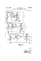
- Figure If is a. schematic circuit. diagram of a radio 2.: receiving system showing one embodiment of the present invention
- Figure 7 is a schematic circuit diagram of a radio receiving'system provided inaccordance with the present invention, having several stages utilized to give additional amplification.
- signal-energy which is received by an antenna lit-sets up alternating currents through the antenna-indu c tor 11. Due to the inductive coupling between the am tenna inductor 1-1' and the input-inductor 12, alternating currents arethereby induced in the input inductor 12. These'latter alternating currents are rectified by a crystal rectifier 13' which may be; of-the type commonly referred to-as- 1N72'. Due to the-rectification by the crystal rectifier, a unidirectional'voltage is established acrossthe loadresistorld having a polarity as shown in Figure l.
- A' portion of the voltage which is to be amplified is developed'acrossthe load resistor 14' and is applied between the emitter electrode 22and'the base electrode 24 of a transistor 20.
- the value of this applie'd'voltage is determined by the setting of the variable tap 15.
- the remainingportion'o-f the load resistor 14 and the shunt connected storage capacitor comprise an energy storing network and in this instance must'have a time constant which is long relative to. the lowest frequency of the amplified signal.
- the crystal rectifier13. is poled in such a direction as. to provide. a reverse bias between the base electrode 24 and the collectorv electrode 23..
- the transistor 20 comprises a semi-conductive body 21 of N type material. If the semi-conductive body 21 were of P type material, the crystal rectifierv 13 would have to be reversed in, polarity. in order. to provide operating potentialsv of a correct polarity.
- the parallel tuned circuit 26 operates as a frequency selecting device and, therefore, provides amplification for, only a definite predetermined frequency.
- amplifier circuit operates in what is commonly referred to as class B, as there exists. no staticbias between. the emitter electrode 22 and the base electrode 24.
- FIG. 2 wherein there is shown a receiving system of the same general characteristic as above described which is capable of operating at greater etficiency.
- Signal energy is received by an antenna 10, and as above discussed, causes alternating currents to be set up in an input inductor 12 which is magnetically coupled as above described to the antenna inductor 11.
- Four crystal rectifiers 32 connected in a bridge circuit operate as a full wave rectifier to rectify the alternating signal currents and thereby establish a direct-current voltage across the load resistor 14 which is connected across one diagonal of the bridge circuit.
- a variable tap 15 on the load resistor 14 is connected to ground and to the base electrode 37 of a junction transistor 33.
- That portion of the load resistor 14 which lies between the variable tap 15 and the end which is connected to a parallel resonant output circuit 26 is shunted by a storage capacitor 16 such as described above in connection with Figure 1.
- a coupling capacitor 29 is connected between the collector electrode 36 of the junction transistor 33 and one of a pair of output terminals 30.
- a bridge rectifier such as this is a full wave rectifier and, therefore, rectifies both the positive and negative portions of the received energy.
- the emitter electrode 35 of the junction transistor 33 be connected to the junction of the bridge rectifier circuit and the inductor 12.
- a bridge rectifier operates to double the frequency of an input wave. Accordingly, this connection of the emitter electrode 35 is necessary to prevent the doubling of the modulation envelope frequency of the received carrier wave.
- the junction transistor 33 is illustrated as a PNP unit having end zones of P type semi-conductive material and an intermediate zone of N type material. However, an N-P-N junction transistor. may be substituted if the polarity of the bridge rectifier is reversed so, that a properly polarized bias is provided.
- FIG 3 there is shown a receiving system which is a modification of that shown in Figure 1.
- a junction type transistor is utilized in an emitter input circuit, and a parallel tuned circuit 38 is connected between the emitter electrode 35 and the base electrode 37 to provide a selection of the signal.
- energy which is applied to the transistorto be amplified is utilized to provide biasing potentials for the transistor 33.
- the high impedance of the parallel resonant tuned circuit 31 at the desired frequency causes the signal energy of this frequency to be impressed between the emitter electrode 35 and the base electrode 37 while the remaining energy in that spectrum of energy which has been received by the antenna system and which has been rectified by the crystal rectifier 13 is impressed almost in its entirety across the network formed by the resistor 14 and the storage capacitor 16 for the purpose of developing biasing potentials.
- the output circuit comprises a load resistor 39 con nected between the collector electrode 36 and ground, and as above described, an output signal may be provided by means of a coupling capacitor 29 connected between the collector electrode 36 and one of a pair of output terminals 30.
- the transistor 33 is operated as a base input amplifier with the input signal being derived from across the tuned circuit 38 and applied between the base electrode 37 and the emitter electrode 35.
- the biasing voltage is developed across the network formed by the load resistor 14 and the storage capacitor 16 and is applied between the emitter electrode 35 and the collector electrode 36.
- An output circuit comprising a pair of headphones 4t) shunted by a bypass capacitor 41 are connected between the collector electrode 36and ground.
- the capacitor 41 may be selected to have a relatively low reactance at radio frequencies and a relatively high reactance at audio frequencies. It can thus be seen that an audio signal will be developed in the earphones which is representative of the amplified modulation envelope of the carrier wave selected by the parallel resonant tuned circuit 38.
- Each of the above described amplifier circuits operates in what is commonly known as class B operation. This is due to the fact that no static bias potential is pro vided between the emitter and base electrodes.
- FIG. 5 there is illustrated a schematic circuit diagram substantially identical with that illustrated in Figure 3 except that the biasing arrangement is provided to enable class A operationof the amplifier cir cuit. This is accomplished by connecting an additional storage capacitor 42 between the variable tap 15 on the load resistor 14 and the junction of the load resistor 14 and the parallel resonant tuned circuit 38.
- the time constant of the circuit comprising the upper portion of the load resistor 14 and the additional storage capacitor 42 circuit is chosen to be relatively long compared to the lowcst frequency of the amplified signals, a bias voltage in the forward direction will be applied between the base electrode 37 and the emitter electrode 35.
- FIG 6 there is shown a schematic circuit diagram which is a modification in accordance with the present invention of the receiving systemshown in Figure 5.
- a second load resistor 44 is connected between the crystal rectifier 13 and the upper end of the load resistance 14.
- a biasing arrangement to provide class A operation as shown in Figure 5 is also utilized in the schematic circuit diagram of Figure 6.
- Signal selection is provided by means of a parallel resonant output circuit 26 connected in the collector electrode circuit in the same manner as the parallel resonant circuit 26 in Figures 1 and 2,
- the schematic circuit diagram illustrated in Figure 7 shows a receiving system comprising a plurality of cascaded receiver andsamplifier circuits capable of providing higher amplification than the above described circuits.
- the first stage of this system which is enclosed within the dotted rectangle 50 comprises a receiving system which is" a modification of that shown in; Figure 6 Inplace of the load resistor- 44*.utilizedin the 'circuit' shown in Figure. 6' there is connected aparallel resonant circuit 3:8
- a coupling capacitor 51? connects the output of the receiving'system 50 to-the base electrode 37a of a second junction transistor 33min a receiving systemwhich is enclosed within the dotted: rectangle 52.
- a parallel resonant tuned input circuit 53 is connected between. the! base electrode 37a and the variable tap 15a of the crystal rectifier load resistance 14a-to provide additional signal selectivity and a suflicient load impedance for the output of the first transistor 33 at the desired frequency.
- a parallel-resonant output circuit 26a is also'provided in the collector electrode circuit of the second-transistor 33a for further-frequency selection.
- the output of this circuit is applied to the base electrode of a third junction transistor 33b in a receiving system which is enclosed within-the dotted rectangle 54.-
- a resistor 55 is connected between the base electrode 37b and the variable tap 1511 on the rectifier load resistor 14b.
- the output of the thirdreceiver amplifier circuit is developed across a collector electrode load impedance 3912 which is connected between the collector electrode 36b and ground.
- the parallel resonant inp'utcircuit 38 is selected by the parallel resonant inp'utcircuit 38 and impressed between the emitter electrode 35' andithe base-electrode37 to be amplified. Further selection of the desired frequency is provided in the output circuit by the parallel resonant output circuit 26 which is connected between the collector electrode 36 and ground.
- the signal voltage thus developed across the parallel resonant output circuit 26 is impressed on the base electrode circuit of the second receiving system 52 by means ofthe parallel resonantcircuit 53.
- This signal voltage is further amplified by the transistor amplifier of the second receiving system circuit enclosed within the dotted rectangle 52, and an. amplified signal voltage is developed across the parallel resonant output circuit 26a.
- the signal which is developed across the parallel resonant output circuit 26a is impressed across the base resistor 55-.
- the signal voltage which is thus impressed across the base resistor 55* is-amplified and appears across the output load resistor 39b;
- biasing potentials are provided by energy received by the antenna system 10, 10a, and 10b.
- the rectifier load resistors 14a and 14b are provided respectively with a pair of capacitors 42a, 42b, 16a and 16b which operate to provide biasing potentials for the second and third transistors 33a and 3311, but which do not provide further signal energy to be amplified.
- the selected signal energy which is to be amplified is provided solely from the first receiving system by the parallel resonant input circuit 38.
- the antenna system crystal, rectifier, and resistor capacitor networks are provided only to establish biasing potentials.
- a receiving system comprising one or more rectifiers connected with a transistor amplifier may provide operating potentials from received electrical energy. It is further seen that this system may be made in compact and durable form and requires no external source of biasing potentials such as batteries.
- the combinationv of,.means including an inductor for receiving carrier wave energy, rectifying-means for rectifying the received carrier wave energy, a load impedance connected in series with said rectifying means, the series combination-ofsaid rectifying. means and said load impedance being connected in shunt withsaid inductor, a storage capacitor connected in shunt withaportion of said load impedance and adapted to be unidirectionally charged by electrical currents flowing through said rectifying means, a semi-conductor device having at least a base electrode and a collector electrode, and meansconnecting said capacitor in circuit with said base electrode and said collector electrode, whereby said collector electrode is operatively biased with respect to said base electrode.
- a receiving system the combination of, means including an inductor for receiving carrier wave energy, rectifying means, a load impedance connected in series with said rectifying means, the series combinationofsaid' rectifying means and said load impedancev being connected in shunt with said'inductor, a storage capacitor connected in shunt'with a portion'of saidload impedance and adapted to be unidirectionally chargedby electrical currents flowing through said rectifying means, a tramsistor device havinga base electrode, a collector electrode and an emitter.
- circuit means connecting said capacitor in circuit with said base electrode and said collector electrode, and further circuit means connecting the remaining portion of said load impedance in circuit with said base electrode and said emitter electrode,- whereby said collector electrode and said emitter electrode are operatively biased with respect to said base electrode.
- a carrier wave receiving circuit a semi-conductor device-adapted toamplify a received signal and having at least a collector electrode, an emitter electrode and a base electrode, a rectifying means coupled to'said receiving circuit, a rectifying means load circuit comprising a first and a second impedance element connected in series arrangement with said rectifying means, a storage capacitor connected in shunt with said-second impedance means and adapted to be charged by a unidirectional current from said rectifying means, said storage capacitor and said second impedance having a time constant which is long relative to the lowest frequency to be amplified, saidsecond impedance element being connected between said emitter electrode and said base electrode, and said first impedance element being connected between said: collector electrode and said base electrode, whereby said operating bias potentials are applied to said'semi-conductor-device in response to said received carrier wave energy.
- a receiving system the combination of, a first inductor adapted to receive radiated carrier wave energy, a second inductor electromagnetically coupled with said first inductor, a unidirectional conducting device, a parallel resonant tuned circuit and aload impedance connected in series arrangement in the order named in shunt with said second inductor, a storage capacitorconnected in shunt with saidload'impedance, a semi-conductor device comprising a semi-conductive body, a base electrode, an emitter electrode and a collector electrode: each.
- said baseelectrode being directly connected to-the common junctionof said unidirectional conducting device and said parallel resonant tuned circuit
- said emitter electrode being directly connected to the common junction of said parallel resonant tuned circuit and said load resistor, and an output load impedance connected between said collector electrode and a common, junction of said second inductor and said load impedance, whereby said collector electrode is biased with respect to said base electrode.
- a receiving system the combination of, a first inductor adapted to receive radiated carrier wave energy, a second inductor electromagnetically coupled with said 7 first inductor, a unidirectional conducting device, a parallel resonant tuned circuit and a load impedance connected in series arrangement in the order named in shunt with said second inductor, a storage capacitor connected in shunt with said load impedance, a semi-conductor device comprising a semi-conductive body, a base electrode, an emitter electrode and a collector electrode each in contact with said semi-conductive body, said emitter electrode being directly connected to the common junction of said unidirectional conducting device and said parallel resonant tuned circuit, said base electrode being directly I connected to the common junction of said parallel resonant tuned circuit and said load resistor, and an output load impedance connected between said collector electrode and a common junction of said second inductor and said load impedance, whereby said collector electrode is biased with respect to said base electrode.
- a first inductor adapted to receive radiated carrier wave energy
- a second inductor electromagnetically coupled with said first inductor, a rectifying element, a first impedance element, a second impedance element connected in series in the order named in shunt with said second inductor, a variable tap on said second impedance element, a first capacitor connected between the junction of said first impedance element and said second impedance element and said variable tap, a second capacitor connected between the junction of said second impedance element and said second inductor and said variable tap, a semi-conduc tor device comprising a semi-conductive body, a base electrodc, an emitter electrode and a collector electrode each in contact with said semi-conductive body, said base electrode being directly connected to said variable tap, said emitter electrode being directly connected to said junction of said first impedance element and said rectifying element, an output impedance element connected between said collector clectrode and said junction of said second impedance element and said second in
- a receiving system the combination of, a first inductor adapted to receive radiated carrier wave energy, a second inductor electromagnetically coupled with said first inductor, a rectifying bridge arrangement connected in shunt with said second inductor, an impedance element connected across one arm of said rectifying bridge arrangement, a variable tap on said impedance element, a storage capacitor connected between said variable tap and one end of said impedance element, a semi-conductor device including a semi-conductive body, a base electrode, an emitter electrode and a collector electrode each in contact with said semi-conductive body, said emitter electrode being directly conductively connected to the junction of said second inductor and said rectifying bridge arrangement, said base electrode being connected to said variable tap, and an output impedance element connected between said collector electrode and said one end of said plifier stages, each comprising means including an in ductor for receiving carrier wave energy, rectifying means I and energy storage means connected in series, the series combination of said rectifying means and energy stormeans being connected in shunt with said in
- a receiving system including a semi-conductor device adapted to amplify received signals and including a semi-conductive body having a plurality of electrodes cooperatively associated therewith, the combination of, means including an inductor for receiving carrier wave energy, rectifying means and energy storage means connected in series, the series combination of said rectifying means and said energy storage means being connected in shunt with said inductor for deriving biasing voltages from said carrier wave energy, said derived biasing voltages being the sole source of energizing potcntials for said device, load impedance means connected with said rectifying means and between a pair of said plurality of electrodes for applying a selected portion of said received signals to said device, and means including said storage means connected between one of said pair of electrodes and another of said plurality of electrodes for applying said derived biasing voltages therebetween to energize said device to amplify said signals.
Description
' Filed Dec. 16, 1952.
2a 12 n 21 A: a '14 4 T- as In OUTPUT J. 1. PAN KOVE RADIATION POWERED TRANSISTOR CIRCUITS 3 Sheets-Sheet 1 OUT/ 07' Jan. 8, 1957.
7 J 1. i V
,T \I l T 26 a I 16' 0UTPU7 INVENTOR.
PANKOVE I I 3 o 5' JACQUES l.
BY ATTORNEY J. I. PANKOVE RADIATION POWERED TRANSISTOR CIRCUITS 3 Sheets-Sheet 2 Jan. 8, 1957.
Filed Dec. 16, 1952 OUTPUT INVENTOR.
ATTORNEY Jan. 8, 1957.v J. l. PANKOVE 2,777,057
RADIATION POWERED TRANSISTOR CIRCUITS Filed Dec. 16, 1952 3 Sheets-Sheet 3 i 146 gfafb i i r I i i i e i ii aab i i lg L i -J INVENTOR.
JACQUES l. PANKOVE ATTORNEY.
United States Patent 9 2,777,057 RADIATION POWEREDTRANSISTOR- CIRCUITS Jacques I: l ankove, Princeton,,N. J., assignor to Radio (Zorporatron of America, a corporation of Delaware Application December 16, 1952; Serial No. 326,295
The terminal fifteenyears'ofthe term'of the. patent to be grantedhas beendisclaimed 10 Claims. ((216.250-20) The present invention relates. generally to highfrequency signal translating circuits and more particularly to. signal receiving; systems employing semi-conductor devices.
Compact receiving systems find wide application in military. operations inthe, field where-information must be sent: to many points from acentral commandpost. Such receiving'systems also' find wide application in civil organizations. such: ascivil *defense and police units which may employ radioicommuni'cationto coordinate a multituderofe operations from a central headquarters. In each of these instances it. isgenerally necessary tomaintain the receiving device'inastandby condition, that is, in such acondltionassto effectively receive signals at-all times. Thisirequirementz of continuous operation necessarily results in the consumption"- of considerable operating power in conventional circuits. In the past it has been custernary" toutilize power storing-devices such as dry cell batteries inportable units-to provide thisoperating power. This resulted in a. rather large'bulk and a continuing maintenance problem.
The requirements-for aportable receiving system include-:small'weightand: bulk for ease of portability and a power source havinga relatively long life and being light andcompact'.
It is, therefore, an object'of this invention to provide a radio receiving system which hasa relatively long, op- Y crating life and which requires no localsource of operating'power.
A further object of this invention is to provide a radiation'powered radio receiving system incorporating a semiconductor amplifier of. improved efficiency.
Another object of this invention is to provide a radiation powered radio receiving system, which is compact, eflicient in operation and. which is relatively inexpensive to manufacture.
In. one aspect of the. presentinvention, atradio receiving system is provided withcircuit means including a.semiconductor device or transistor for.- receiving-and. amplifying highfrequency signal. modulated: carrier Waves. A non-linear conducting device, such as, for example, a crystal rectifier is provided to rectify the receivedcarrier wave. A portion of the rectified energy is stored in an energy storage devicesuch as a capacitor and is. used to provide operating, voltages: for the, transistor. amplifier. A. tunable circuit is provided in. conjunction with, the: amplifierfor selecting a carrier waveof predetermined frequency to be amplified.
The novel features tliatare. considered characteristic of this invention are set forth with particularity in the appended claims. Theiinvention itself, however, both,as to its organization and'metliodof'operation, as well as addi- 'tional objects and advantages thereof, will best be understood from the following description when. read in connection with the accompanying drawings in which:
Figure If is a. schematic circuit. diagram of a radio 2.: receiving system showing one embodiment of the present invention;
Figure 2 is a schematic circuit diagra mof aradio -re-' ceiving system provided in accordance withthe present invention and=having a greater-eificiency than the embodimentillustrated in Figure 1;
Figures 3, 4, 5 and dare schematic circuit diagrams of additional embodiments of a radio-receiving system provided inaccordance with the present invention; and
Figure 7'is a schematic circuit diagram of a radio receiving'system provided inaccordance with the present invention, having several stages utilized to give additional amplification. i
Referring now to the drawings, and in particular to Figure 1, signal-energy which is received by an antenna lit-sets up alternating currents through the antenna-indu c= tor 11. Due to the inductive coupling between the am tenna inductor 1-1' and the input-inductor 12, alternating currents arethereby induced in the input inductor 12. These'latter alternating currents are rectified by a crystal rectifier 13' which may be; of-the type commonly referred to-as- 1N72'. Due to the-rectification by the crystal rectifier, a unidirectional'voltage is established acrossthe loadresistorld having a polarity as shown in Figure l. A' portion of the voltage which is to be amplified is developed'acrossthe load resistor 14' and is applied between the emitter electrode 22and'the base electrode 24 of a transistor 20. The value of this applie'd'voltage is determined by the setting of the variable tap 15. The remainingportion'o-f the load resistor 14 and the shunt connected storage capacitor comprise an energy storing network and in this instance must'have a time constant which is long relative to. the lowest frequency of the amplified signal.
When such a network is provided which has a relatively long time constant, there will be developed across the storage capacitor 16 a voltage which is substantially uniform and which has a polarity such as shown.
It can be seen that'this voltage will be applied between the base electrode 24and the collector electrode 23 of the-transistor 2'0' thus providing an operating bias between these electrodes.
It is noted at this time that the crystal rectifier13. is poled in such a direction as. to provide. a reverse bias between the base electrode 24 and the collectorv electrode 23.. With the polarities as shownin the drawing, it is assumed that the transistor 20 comprises a semi-conductive body 21 of N type material. If the semi-conductive body 21 were of P type material, the crystal rectifierv 13 would have to be reversed in, polarity. in order. to provide operating potentialsv of a correct polarity. a
' The voltage which isdeveloped. across that portion of the load resistor 14, whichisbetween-the variable tap-15 and the crystalrectifier. 13; is. applied between the emitter electrode 22 and the base electrode 24 and is amplified and appears in amplifiedform across the parallel tuned output circuit. 26. The parallel tuned circuit 26 operates as a frequency selecting device and, therefore, provides amplification for, only a definite predetermined frequency.
It is noted that this. amplifier circuit operates in what is commonly referred to as class B, as there exists. no staticbias between. the emitter electrode 22 and the base electrode 24.
It isrpossible to provide a. receiving system which. operates in accordance with the present invention asabove described by having an antenna system which is broadly tuned and which, therefore, accepts energy from a wide frequency spectrum. Thislarge band of energy is'openated on by the crystal rectifier 13, the load resistor 14 and, the storage capacitor 16.to provide the necessary operating potentials. However, only anarrowtpoe aver per tion of the received energy is selected and amplified by the transistor amplifier due to the parallel tuned output circuit 26. It is thus possible to provide a compact receiver-which receives its operating power solely from radiated energy.
Referring now to Figure 2 wherein there is shown a receiving system of the same general characteristic as above described which is capable of operating at greater etficiency. Signal energy is received by an antenna 10, and as above discussed, causes alternating currents to be set up in an input inductor 12 which is magnetically coupled as above described to the antenna inductor 11. Four crystal rectifiers 32 connected in a bridge circuit operate as a full wave rectifier to rectify the alternating signal currents and thereby establish a direct-current voltage across the load resistor 14 which is connected across one diagonal of the bridge circuit. A variable tap 15 on the load resistor 14 is connected to ground and to the base electrode 37 of a junction transistor 33. That portion of the load resistor 14 which lies between the variable tap 15 and the end which is connected to a parallel resonant output circuit 26 is shunted by a storage capacitor 16 such as described above in connection with Figure 1. A coupling capacitor 29 is connected between the collector electrode 36 of the junction transistor 33 and one of a pair of output terminals 30.
The operation of the circuit just described is similar tothe operation of the circuit described inFigure 1 of the drawing. However, due to the greater efficiency of the bridge rectifier, the overall efiiciency of the circuit is enhanced.
As is well known in the art, a bridge rectifier such as this is a full wave rectifier and, therefore, rectifies both the positive and negative portions of the received energy.
It is, therefore, necessary that the emitter electrode 35 of the junction transistor 33 be connected to the junction of the bridge rectifier circuit and the inductor 12. As is well known in the rectifier art, a bridge rectifier operates to double the frequency of an input wave. Accordingly, this connection of the emitter electrode 35 is necessary to prevent the doubling of the modulation envelope frequency of the received carrier wave.
The junction transistor 33 is illustrated as a PNP unit having end zones of P type semi-conductive material and an intermediate zone of N type material. However, an N-P-N junction transistor. may be substituted if the polarity of the bridge rectifier is reversed so, that a properly polarized bias is provided.
In Figure 3 there is shown a receiving system which is a modification of that shown in Figure 1. Inthis instance, a junction type transistor is utilized in an emitter input circuit, and a parallel tuned circuit 38 is connected between the emitter electrode 35 and the base electrode 37 to provide a selection of the signal. energy which is applied to the transistorto be amplified. Further, as this circuit provides a low impedance at other frequencies, a greater portion of the received energy, which is not to be selected for amplification, is utilized to provide biasing potentials for the transistor 33. In other words, the high impedance of the parallel resonant tuned circuit 31 at the desired frequency causes the signal energy of this frequency to be impressed between the emitter electrode 35 and the base electrode 37 while the remaining energy in that spectrum of energy which has been received by the antenna system and which has been rectified by the crystal rectifier 13 is impressed almost in its entirety across the network formed by the resistor 14 and the storage capacitor 16 for the purpose of developing biasing potentials. i
The output circuit comprises a load resistor 39 con nected between the collector electrode 36 and ground, and as above described, an output signal may be provided by means of a coupling capacitor 29 connected between the collector electrode 36 and one of a pair of output terminals 30.
it should be readily apparent from the above discussion that the circuit illustrated in Figure 3 is more efiicient than the circuit illustratedin Figure 1 due to the fact that the load resistor 14 is used in its entirety for developing biasing potentials.
Referring now to Figure 4, the transistor 33 is operated as a base input amplifier with the input signal being derived from across the tuned circuit 38 and applied between the base electrode 37 and the emitter electrode 35. The biasing voltage is developed across the network formed by the load resistor 14 and the storage capacitor 16 and is applied between the emitter electrode 35 and the collector electrode 36.
An output circuit comprising a pair of headphones 4t) shunted by a bypass capacitor 41 are connected between the collector electrode 36and ground. The capacitor 41 may be selected to have a relatively low reactance at radio frequencies and a relatively high reactance at audio frequencies. It can thus be seen that an audio signal will be developed in the earphones which is representative of the amplified modulation envelope of the carrier wave selected by the parallel resonant tuned circuit 38.
Each of the above described amplifier circuits operates in what is commonly known as class B operation. This is due to the fact that no static bias potential is pro vided between the emitter and base electrodes.
However, in Figure 5 there is illustrated a schematic circuit diagram substantially identical with that illustrated in Figure 3 except that the biasing arrangement is provided to enable class A operationof the amplifier cir cuit. This is accomplished by connecting an additional storage capacitor 42 between the variable tap 15 on the load resistor 14 and the junction of the load resistor 14 and the parallel resonant tuned circuit 38.
It can thus readily be seen that it": the time constant of the circuit comprising the upper portion of the load resistor 14 and the additional storage capacitor 42 circuit is chosen to be relatively long compared to the lowcst frequency of the amplified signals, a bias voltage in the forward direction will be applied between the base electrode 37 and the emitter electrode 35.
In Figure 6 there is shown a schematic circuit diagram which is a modification in accordance with the present invention of the receiving systemshown in Figure 5. In place of the parallel resonant tuned circuit 38, a second load resistor 44 is connected between the crystal rectifier 13 and the upper end of the load resistance 14. A biasing arrangement to provide class A operation as shown in Figure 5 is also utilized in the schematic circuit diagram of Figure 6. Signal selection, however, is provided by means of a parallel resonant output circuit 26 connected in the collector electrode circuit in the same manner as the parallel resonant circuit 26 in Figures 1 and 2,
It can thus be seen that energy received by the antenna system will set up currents which are rectified by the crystal rectifier 13. Biasing voltages are accordingly developed across the series arrangement of the load resistors 44 and 14. That portion of the voltage, which is developed across the second load resistor 44, is in the form of a signal voltage impressed between the base electrode 37 and the emitter electrode 35. The remaining portion of the voltage, which is developed across the load resistor 14, is utilized to provide a bias voltage for the transistor to establish class A operation. The desired carrier wave energy is selected by the operation of the parallel resonant output circuit 26 and an amplified version thereof will appear across the output terminals 30.
The schematic circuit diagram illustrated in Figure 7 shows a receiving system comprising a plurality of cascaded receiver andsamplifier circuits capable of providing higher amplification than the above described circuits.
The first stage of this system, which is enclosed within the dotted rectangle 50 comprises a receiving system which is" a modification of that shown in; Figure 6 Inplace of the load resistor- 44*.utilizedin the 'circuit' shown in Figure. 6' there is connected aparallel resonant circuit 3:8
to-enable more precise selection of the desired-signal frequency. A coupling capacitor 51? connects the output of the receiving'system 50 to-the base electrode 37a of a second junction transistor 33min a receiving systemwhich is enclosed within the dotted: rectangle 52. A parallel resonant tuned input circuit 53 is connected between. the! base electrode 37a and the variable tap 15a of the crystal rectifier load resistance 14a-to provide additional signal selectivity and a suflicient load impedance for the output of the first transistor 33 at the desired frequency.
A parallel-resonant output circuit 26a is also'provided in the collector electrode circuit of the second-transistor 33a for further-frequency selection. The output of this circuit is applied to the base electrode of a third junction transistor 33b in a receiving system which is enclosed within-the dotted rectangle 54.- In this instance a resistor 55 is connected between the base electrode 37b and the variable tap 1511 on the rectifier load resistor 14b.
The output of the thirdreceiver amplifier circuit is developed across a collector electrode load impedance 3912 which is connected between the collector electrode 36b and ground.
The operation of the above described circuit is asfollows: Energy which is received by the antenna systems 10, 10a, and 10b is rectified in each of the receiving systerns-by the crystal rectifiers 13, 13a and 13b, thereby developing bias voltages across the rectifier load impedances 14, 14a, and 14b to provide class A operation.
Also, in the receiving system enclosed withinthe dotted rectangle 50, a portion of this energy is selected by the parallel resonant inp'utcircuit 38 and impressed between the emitter electrode 35' andithe base-electrode37 to be amplified. Further selection of the desired frequency is provided in the output circuit by the parallel resonant output circuit 26 which is connected between the collector electrode 36 and ground. The signal voltage thus developed across the parallel resonant output circuit 26 is impressed on the base electrode circuit of the second receiving system 52 by means ofthe parallel resonantcircuit 53. This signal voltage is further amplified by the transistor amplifier of the second receiving system circuit enclosed within the dotted rectangle 52, and an. amplified signal voltage is developed across the parallel resonant output circuit 26a.
Further frequency selection is not necessary. Accordingly, the signal which is developed across the parallel resonant output circuit 26a is impressed across the base resistor 55-. The signal voltage which is thus impressed across the base resistor 55* is-amplified and appears across the output load resistor 39b;
As above mentioned, biasing potentials are provided by energy received by the antenna system 10, 10a, and 10b. It is noted that in thesecond and third receiving systems, the rectifier load resistors 14a and 14b are provided respectively with a pair of capacitors 42a, 42b, 16a and 16b which operate to provide biasing potentials for the second and third transistors 33a and 3311, but which do not provide further signal energy to be amplified. The selected signal energy which is to be amplified is provided solely from the first receiving system by the parallel resonant input circuit 38. In each of the other circuits the antenna system crystal, rectifier, and resistor capacitor networks are provided only to establish biasing potentials.
It is thus seen that a receiving system comprising one or more rectifiers connected with a transistor amplifier may provide operating potentials from received electrical energy. It is further seen that this system may be made in compact and durable form and requires no external source of biasing potentials such as batteries.
What is claimed is:
1. In av receiving. system, the combinationv of,.means including an inductor for receiving carrier wave energy, rectifying-means for rectifying the received carrier wave energy, a load impedance connected in series with said rectifying means, the series combination-ofsaid rectifying. means and said load impedance being connected in shunt withsaid inductor, a storage capacitor connected in shunt withaportion of said load impedance and adapted to be unidirectionally charged by electrical currents flowing through said rectifying means, a semi-conductor device having at least a base electrode and a collector electrode, and meansconnecting said capacitor in circuit with said base electrode and said collector electrode, whereby said collector electrode is operatively biased with respect to said base electrode.
2. In a receiving system, the combination of, means including an inductor for receiving carrier wave energy, rectifying means, a load impedance connected in series with said rectifying means, the series combinationofsaid' rectifying means and said load impedancev being connected in shunt with said'inductor, a storage capacitor connected in shunt'with a portion'of saidload impedance and adapted to be unidirectionally chargedby electrical currents flowing through said rectifying means, a tramsistor device havinga base electrode, a collector electrode and an emitter. electrode, circuit means connecting said capacitor in circuit with said base electrode and said collector electrode, and further circuit means connecting the remaining portion of said load impedance in circuit with said base electrode and said emitter electrode,- whereby said collector electrode and said emitter electrode are operatively biased with respect to said base electrode.
3. In-a receiving system, the combinationof, a carrier wave receiving circuit, a semi-conductor device-adapted toamplify a received signal and having at least a collector electrode, an emitter electrode and a base electrode, a rectifying means coupled to'said receiving circuit, a rectifying means load circuit comprising a first and a second impedance element connected in series arrangement with said rectifying means, a storage capacitor connected in shunt with said-second impedance means and adapted to be charged by a unidirectional current from said rectifying means, said storage capacitor and said second impedance having a time constant which is long relative to the lowest frequency to be amplified, saidsecond impedance element being connected between said emitter electrode and said base electrode, and said first impedance element being connected between said: collector electrode and said base electrode, whereby said operating bias potentials are applied to said'semi-conductor-device in response to said received carrier wave energy.
4. In a receiving system, the combination of, a first inductor adapted to receive radiated carrier wave energy, a second inductor electromagnetically coupled with said first inductor, a unidirectional conducting device, a parallel resonant tuned circuit and aload impedance connected in series arrangement in the order named in shunt with said second inductor, a storage capacitorconnected in shunt with saidload'impedance, a semi-conductor device comprising a semi-conductive body, a base electrode, an emitter electrode and a collector electrode: each. in contact with said semi-conductive body, said baseelectrode being directly connected to-the common junctionof said unidirectional conducting device and said parallel resonant tuned circuit, said emitter electrode being directly connected to the common junction of said parallel resonant tuned circuit and said load resistor, and an output load impedance connected between said collector electrode and a common, junction of said second inductor and said load impedance, whereby said collector electrode is biased with respect to said base electrode.
5. In a receiving system, the combination of, a first inductor adapted to receive radiated carrier wave energy, a second inductor electromagnetically coupled with said 7 first inductor, a unidirectional conducting device, a parallel resonant tuned circuit and a load impedance connected in series arrangement in the order named in shunt with said second inductor, a storage capacitor connected in shunt with said load impedance, a semi-conductor device comprising a semi-conductive body, a base electrode, an emitter electrode and a collector electrode each in contact with said semi-conductive body, said emitter electrode being directly connected to the common junction of said unidirectional conducting device and said parallel resonant tuned circuit, said base electrode being directly I connected to the common junction of said parallel resonant tuned circuit and said load resistor, and an output load impedance connected between said collector electrode and a common junction of said second inductor and said load impedance, whereby said collector electrode is biased with respect to said base electrode.
6. In a receiving system, the combination of, a first inductor adapted to receive radiated carrier wave energy, a second inductor electromagnetically coupled with said first inductor, a rectifying element, a first impedance element, a second impedance element connected in series in the order named in shunt with said second inductor, a variable tap on said second impedance element, a first capacitor connected between the junction of said first impedance element and said second impedance element and said variable tap, a second capacitor connected between the junction of said second impedance element and said second inductor and said variable tap, a semi-conduc tor device comprising a semi-conductive body, a base electrodc, an emitter electrode and a collector electrode each in contact with said semi-conductive body, said base electrode being directly connected to said variable tap, said emitter electrode being directly connected to said junction of said first impedance element and said rectifying element, an output impedance element connected between said collector clectrode and said junction of said second impedance element and said second inductor.
7. In a receiving system, the combination of, a first inductor adapted to receive radiated carrier wave energy, a second inductor electromagnetically coupled with said first inductor, a rectifying bridge arrangement connected in shunt with said second inductor, an impedance element connected across one arm of said rectifying bridge arrangement, a variable tap on said impedance element, a storage capacitor connected between said variable tap and one end of said impedance element, a semi-conductor device including a semi-conductive body, a base electrode, an emitter electrode and a collector electrode each in contact with said semi-conductive body, said emitter electrode being directly conductively connected to the junction of said second inductor and said rectifying bridge arrangement, said base electrode being connected to said variable tap, and an output impedance element connected between said collector electrode and said one end of said plifier stages, each comprising means including an in ductor for receiving carrier wave energy, rectifying means I and energy storage means connected in series, the series combination of said rectifying means and energy stormeans being connected in shunt with said inductor for deriving biasing voltages from said carrier wave energy, a semi-conductor device including a semi-conductive body having a plurality of electrodes cooperatively associated therewith, a first circuit means connecting said energy storage means between a pair of said plurality of electrodes for operatively biasing said device, one of said stages including frequency selective means coupled between one of said pair of electrodes and another of said plurality of electrodes for selecting a portion of said carrier wave energy as signal energy to be amplified by each of said stages.
10. In a receiving system including a semi-conductor device adapted to amplify received signals and including a semi-conductive body having a plurality of electrodes cooperatively associated therewith, the combination of, means including an inductor for receiving carrier wave energy, rectifying means and energy storage means connected in series, the series combination of said rectifying means and said energy storage means being connected in shunt with said inductor for deriving biasing voltages from said carrier wave energy, said derived biasing voltages being the sole source of energizing potcntials for said device, load impedance means connected with said rectifying means and between a pair of said plurality of electrodes for applying a selected portion of said received signals to said device, and means including said storage means connected between one of said pair of electrodes and another of said plurality of electrodes for applying said derived biasing voltages therebetween to energize said device to amplify said signals.
References Cited in the file of this patent UNITED STATES PATENTS 2,144,606 Burnside Jan. 24, 1939 2,293,480 Tovar Aug. 18, 1942 2,373,569 Kannenberg Apr. 10, 1945 2,644,893 Gehman .a July 7, 1953 2,647,957 Mallinckrodt Aug. 4, 1953 OTHER REFERENCES A Crystal Receiver With Transistor Amplifier, Radio and Television News, January 1950, pp. 38, 39, 153, 154, 155.
Junction Transistor Equivalent Circuits and Vacuum Tube Analogy, by Giacoletto, pp. 1490 to 1493 of Free. I. R. 13., vol. 40, No. 11, November 1952.
Priority Applications (1)
| Application Number | Priority Date | Filing Date | Title |
|---|---|---|---|
| US326295A US2777057A (en) | 1952-12-16 | 1952-12-16 | Radiation powered transistor circuits |
Applications Claiming Priority (1)
| Application Number | Priority Date | Filing Date | Title |
|---|---|---|---|
| US326295A US2777057A (en) | 1952-12-16 | 1952-12-16 | Radiation powered transistor circuits |
Publications (1)
| Publication Number | Publication Date |
|---|---|
| US2777057A true US2777057A (en) | 1957-01-08 |
Family
ID=23271622
Family Applications (1)
| Application Number | Title | Priority Date | Filing Date |
|---|---|---|---|
| US326295A Expired - Lifetime US2777057A (en) | 1952-12-16 | 1952-12-16 | Radiation powered transistor circuits |
Country Status (1)
| Country | Link |
|---|---|
| US (1) | US2777057A (en) |
Cited By (38)
| Publication number | Priority date | Publication date | Assignee | Title |
|---|---|---|---|---|
| US2837740A (en) * | 1957-01-30 | 1958-06-03 | Haller Raymond And Brown Inc | Proportional gate circuit |
| US2851592A (en) * | 1952-12-03 | 1958-09-09 | Rca Corp | Carrier wave powered radio transceiver circuits |
| US2863068A (en) * | 1954-08-27 | 1958-12-02 | Gen Electric | Signal responsive network |
| US2876366A (en) * | 1953-12-28 | 1959-03-03 | Bell Telephone Labor Inc | Semiconductor switching devices |
| US2885575A (en) * | 1956-01-28 | 1959-05-05 | Philips Corp | Limiting circuit |
| US2891156A (en) * | 1956-07-25 | 1959-06-16 | Motorola Inc | Detector circuit |
| US2906968A (en) * | 1957-12-27 | 1959-09-29 | Montgomery George Franklin | Transistor-controlled reactance modulator |
| US2918573A (en) * | 1956-09-10 | 1959-12-22 | Dresser Ind | Passive self-powered transistor detector-amplifier |
| US2947881A (en) * | 1957-03-07 | 1960-08-02 | Cutler Hammer Inc | Time delay systems utilizing transistors |
| US2950357A (en) * | 1956-05-01 | 1960-08-23 | Robert E Mitchell | Electronic sound transmitting device |
| US2969470A (en) * | 1956-11-06 | 1961-01-24 | Hazeltine Research Inc | Alternating-signal generator |
| US2981833A (en) * | 1955-03-17 | 1961-04-25 | Jr George W Bryan | Sound powered radio transmitter |
| US2995669A (en) * | 1958-04-03 | 1961-08-08 | Philips Corp | Transistorized pulse generator |
| US2996680A (en) * | 1958-05-01 | 1961-08-15 | Gen Electric Co Ltd | Transistorized pulse demodulator |
| US2997535A (en) * | 1958-11-12 | 1961-08-22 | Packard Bell Electronics Corp | Signal powered television remote control system |
| US3002144A (en) * | 1957-08-21 | 1961-09-26 | Boeing Co | Controllable impedances |
| US3002087A (en) * | 1953-05-01 | 1961-09-26 | Itt | Self-powered radio transmitter |
| US3046486A (en) * | 1959-04-06 | 1962-07-24 | Gen Electric | Signal receiving apparatus |
| DE1160497B (en) * | 1957-09-12 | 1964-01-02 | Fernseh Gmbh | Circuit arrangement for reversing unidirectional waves |
| US3118145A (en) * | 1960-01-11 | 1964-01-14 | Gilbert C Nee | Carrier powered paging system |
| US3141140A (en) * | 1959-05-20 | 1964-07-14 | Acoustica Associates Inc | A. c. operated transistor oscillator or amplifier circuits |
| US3205452A (en) * | 1962-01-03 | 1965-09-07 | Zenith Radio Corp | Unidirectionally conductive device for varying the output signal frequency of a signal generator |
| US3209081A (en) * | 1961-10-02 | 1965-09-28 | Behrman A Ducote | Subcutaneously implanted electronic device |
| US3212033A (en) * | 1960-10-25 | 1965-10-12 | Westinghouse Electric Corp | Integrated circuit semiconductor narrow band notch filter |
| US3231804A (en) * | 1961-10-17 | 1966-01-25 | Charles F Weisgerber | Servo control device |
| US3381235A (en) * | 1965-03-22 | 1968-04-30 | Webster Electric Co Inc | Amplifier having feedback bias control circuit |
| US3399397A (en) * | 1966-01-07 | 1968-08-27 | Josephson Elliot | Apparatus for sending and receiving a signal on an a-c line |
| US3436640A (en) * | 1963-07-31 | 1969-04-01 | Raymond P Murray | Function generator apparatus |
| US3478605A (en) * | 1964-10-22 | 1969-11-18 | Vernon H Siegel | Accelerometer and pickoff system |
| US3836855A (en) * | 1958-05-05 | 1974-09-17 | Singer Co | Modulating system |
| FR2545207A1 (en) * | 1974-06-25 | 1984-11-02 | France Etat Armement | Programming and energy-transfer device for weapon systems and projectile for weapon systems equipped with such a device |
| DE3324957A1 (en) * | 1983-07-11 | 1985-01-31 | Sennheiser Electronic Kg, 3002 Wedemark | Method for supplying a portable slave station of a data transmission system with power |
| US4534039A (en) * | 1982-02-26 | 1985-08-06 | Develcon Electronics Ltd. | Dataset powered by control and data signals from data terminal |
| US4677646A (en) * | 1982-02-26 | 1987-06-30 | Develcon Electronics Ltd. | Dataset powered by control and data signals from data terminal |
| FR2618584A1 (en) * | 1987-07-20 | 1989-01-27 | Tabuteau Christian | Radio controlled receiver without a battery with current recreation |
| US5125077A (en) * | 1983-11-02 | 1992-06-23 | Microsoft Corporation | Method of formatting data from a mouse |
| US20090214064A1 (en) * | 2008-02-25 | 2009-08-27 | Zounds, Inc. | RF power supply for hearing aids |
| US20110193420A1 (en) * | 2004-05-12 | 2011-08-11 | Makoto Ishida | Power generation circuit using electromagnetic wave |
Citations (5)
| Publication number | Priority date | Publication date | Assignee | Title |
|---|---|---|---|---|
| US2144606A (en) * | 1936-12-10 | 1939-01-24 | Rca Corp | Constant bias diode detector circuit |
| US2293480A (en) * | 1937-03-31 | 1942-08-18 | Tovar Jorge Guzman | High frequency amplifier |
| US2373569A (en) * | 1943-01-23 | 1945-04-10 | Bell Telephone Labor Inc | Wave translating system |
| US2644893A (en) * | 1952-06-02 | 1953-07-07 | Rca Corp | Semiconductor pulse memory circuits |
| US2647957A (en) * | 1949-06-01 | 1953-08-04 | Bell Telephone Labor Inc | Transistor circuit |
-
1952
- 1952-12-16 US US326295A patent/US2777057A/en not_active Expired - Lifetime
Patent Citations (5)
| Publication number | Priority date | Publication date | Assignee | Title |
|---|---|---|---|---|
| US2144606A (en) * | 1936-12-10 | 1939-01-24 | Rca Corp | Constant bias diode detector circuit |
| US2293480A (en) * | 1937-03-31 | 1942-08-18 | Tovar Jorge Guzman | High frequency amplifier |
| US2373569A (en) * | 1943-01-23 | 1945-04-10 | Bell Telephone Labor Inc | Wave translating system |
| US2647957A (en) * | 1949-06-01 | 1953-08-04 | Bell Telephone Labor Inc | Transistor circuit |
| US2644893A (en) * | 1952-06-02 | 1953-07-07 | Rca Corp | Semiconductor pulse memory circuits |
Cited By (39)
| Publication number | Priority date | Publication date | Assignee | Title |
|---|---|---|---|---|
| US2851592A (en) * | 1952-12-03 | 1958-09-09 | Rca Corp | Carrier wave powered radio transceiver circuits |
| US3002087A (en) * | 1953-05-01 | 1961-09-26 | Itt | Self-powered radio transmitter |
| US2876366A (en) * | 1953-12-28 | 1959-03-03 | Bell Telephone Labor Inc | Semiconductor switching devices |
| US2863068A (en) * | 1954-08-27 | 1958-12-02 | Gen Electric | Signal responsive network |
| US2981833A (en) * | 1955-03-17 | 1961-04-25 | Jr George W Bryan | Sound powered radio transmitter |
| US2885575A (en) * | 1956-01-28 | 1959-05-05 | Philips Corp | Limiting circuit |
| US2950357A (en) * | 1956-05-01 | 1960-08-23 | Robert E Mitchell | Electronic sound transmitting device |
| US2891156A (en) * | 1956-07-25 | 1959-06-16 | Motorola Inc | Detector circuit |
| US2918573A (en) * | 1956-09-10 | 1959-12-22 | Dresser Ind | Passive self-powered transistor detector-amplifier |
| US2969470A (en) * | 1956-11-06 | 1961-01-24 | Hazeltine Research Inc | Alternating-signal generator |
| US2837740A (en) * | 1957-01-30 | 1958-06-03 | Haller Raymond And Brown Inc | Proportional gate circuit |
| US2947881A (en) * | 1957-03-07 | 1960-08-02 | Cutler Hammer Inc | Time delay systems utilizing transistors |
| US3002144A (en) * | 1957-08-21 | 1961-09-26 | Boeing Co | Controllable impedances |
| DE1160497B (en) * | 1957-09-12 | 1964-01-02 | Fernseh Gmbh | Circuit arrangement for reversing unidirectional waves |
| US2906968A (en) * | 1957-12-27 | 1959-09-29 | Montgomery George Franklin | Transistor-controlled reactance modulator |
| US2995669A (en) * | 1958-04-03 | 1961-08-08 | Philips Corp | Transistorized pulse generator |
| US2996680A (en) * | 1958-05-01 | 1961-08-15 | Gen Electric Co Ltd | Transistorized pulse demodulator |
| US3836855A (en) * | 1958-05-05 | 1974-09-17 | Singer Co | Modulating system |
| US2997535A (en) * | 1958-11-12 | 1961-08-22 | Packard Bell Electronics Corp | Signal powered television remote control system |
| US3046486A (en) * | 1959-04-06 | 1962-07-24 | Gen Electric | Signal receiving apparatus |
| US3141140A (en) * | 1959-05-20 | 1964-07-14 | Acoustica Associates Inc | A. c. operated transistor oscillator or amplifier circuits |
| US3118145A (en) * | 1960-01-11 | 1964-01-14 | Gilbert C Nee | Carrier powered paging system |
| US3212033A (en) * | 1960-10-25 | 1965-10-12 | Westinghouse Electric Corp | Integrated circuit semiconductor narrow band notch filter |
| US3209081A (en) * | 1961-10-02 | 1965-09-28 | Behrman A Ducote | Subcutaneously implanted electronic device |
| US3231804A (en) * | 1961-10-17 | 1966-01-25 | Charles F Weisgerber | Servo control device |
| US3205452A (en) * | 1962-01-03 | 1965-09-07 | Zenith Radio Corp | Unidirectionally conductive device for varying the output signal frequency of a signal generator |
| US3436640A (en) * | 1963-07-31 | 1969-04-01 | Raymond P Murray | Function generator apparatus |
| US3478605A (en) * | 1964-10-22 | 1969-11-18 | Vernon H Siegel | Accelerometer and pickoff system |
| US3381235A (en) * | 1965-03-22 | 1968-04-30 | Webster Electric Co Inc | Amplifier having feedback bias control circuit |
| US3399397A (en) * | 1966-01-07 | 1968-08-27 | Josephson Elliot | Apparatus for sending and receiving a signal on an a-c line |
| FR2545207A1 (en) * | 1974-06-25 | 1984-11-02 | France Etat Armement | Programming and energy-transfer device for weapon systems and projectile for weapon systems equipped with such a device |
| US4534039A (en) * | 1982-02-26 | 1985-08-06 | Develcon Electronics Ltd. | Dataset powered by control and data signals from data terminal |
| US4677646A (en) * | 1982-02-26 | 1987-06-30 | Develcon Electronics Ltd. | Dataset powered by control and data signals from data terminal |
| DE3324957A1 (en) * | 1983-07-11 | 1985-01-31 | Sennheiser Electronic Kg, 3002 Wedemark | Method for supplying a portable slave station of a data transmission system with power |
| US5125077A (en) * | 1983-11-02 | 1992-06-23 | Microsoft Corporation | Method of formatting data from a mouse |
| FR2618584A1 (en) * | 1987-07-20 | 1989-01-27 | Tabuteau Christian | Radio controlled receiver without a battery with current recreation |
| US20110193420A1 (en) * | 2004-05-12 | 2011-08-11 | Makoto Ishida | Power generation circuit using electromagnetic wave |
| US8513927B2 (en) * | 2004-05-12 | 2013-08-20 | Makoto Ishida | Power generation circuit for generating and storing electric power utilizing radio wave energy |
| US20090214064A1 (en) * | 2008-02-25 | 2009-08-27 | Zounds, Inc. | RF power supply for hearing aids |
Similar Documents
| Publication | Publication Date | Title |
|---|---|---|
| US2777057A (en) | Radiation powered transistor circuits | |
| US2851592A (en) | Carrier wave powered radio transceiver circuits | |
| US2771584A (en) | Frequency-controlled transistor oscillators | |
| US2570939A (en) | Semiconductor reactance circuit | |
| US2866892A (en) | Detector circuit in which increasing rectified signal causes decreasing collector current | |
| US3020493A (en) | Frequency modulation circuit | |
| US3023378A (en) | Voltage-controlled capacitance converter-modulator | |
| US2934641A (en) | Stabilization means for semi-conductor signal conveying circuits | |
| US2770728A (en) | Semi-conductor frequency multiplier circuit | |
| US3345570A (en) | Transistor protection circuit for radio transmitter | |
| US2729708A (en) | Band-pass amplifier systems | |
| US2885544A (en) | Automatic gain control using voltage drop in biasing circuit common to plural transistor stages | |
| US2885495A (en) | Emitter coupled transistor amplifier | |
| US2750508A (en) | Transistor oscillator circuit | |
| US2920189A (en) | Semiconductor signal translating circuit | |
| US2666902A (en) | Frequency modulator transistor circuits | |
| US3335370A (en) | High level amplitude modulation of transistor radio frequency amplifiers | |
| US2916616A (en) | Reflex amplifier-detector stage | |
| US3258695A (en) | Reflex receiver | |
| US2810110A (en) | Semi-conductor modulation circuits | |
| US2886653A (en) | Amplitude modulated oscillator systems | |
| US2956159A (en) | Detector system | |
| US2924778A (en) | Semi-conductor signal conveying circuits | |
| US2941076A (en) | Compound demodulator | |
| US3061785A (en) | Transistor protecting circuit |