US3890537A - Solid state chopper ballast for gaseous discharge lamps - Google Patents
Solid state chopper ballast for gaseous discharge lamps Download PDFInfo
- Publication number
- US3890537A US3890537A US430088A US43008874A US3890537A US 3890537 A US3890537 A US 3890537A US 430088 A US430088 A US 430088A US 43008874 A US43008874 A US 43008874A US 3890537 A US3890537 A US 3890537A
- Authority
- US
- United States
- Prior art keywords
- voltage
- circuit
- current
- power
- control
- Prior art date
- Legal status (The legal status is an assumption and is not a legal conclusion. Google has not performed a legal analysis and makes no representation as to the accuracy of the status listed.)
- Expired - Lifetime
Links
Images


Classifications
-
- H—ELECTRICITY
- H02—GENERATION; CONVERSION OR DISTRIBUTION OF ELECTRIC POWER
- H02M—APPARATUS FOR CONVERSION BETWEEN AC AND AC, BETWEEN AC AND DC, OR BETWEEN DC AND DC, AND FOR USE WITH MAINS OR SIMILAR POWER SUPPLY SYSTEMS; CONVERSION OF DC OR AC INPUT POWER INTO SURGE OUTPUT POWER; CONTROL OR REGULATION THEREOF
- H02M1/00—Details of apparatus for conversion
- H02M1/42—Circuits or arrangements for compensating for or adjusting power factor in converters or inverters
- H02M1/4208—Arrangements for improving power factor of AC input
-
- H—ELECTRICITY
- H05—ELECTRIC TECHNIQUES NOT OTHERWISE PROVIDED FOR
- H05B—ELECTRIC HEATING; ELECTRIC LIGHT SOURCES NOT OTHERWISE PROVIDED FOR; CIRCUIT ARRANGEMENTS FOR ELECTRIC LIGHT SOURCES, IN GENERAL
- H05B41/00—Circuit arrangements or apparatus for igniting or operating discharge lamps
- H05B41/14—Circuit arrangements
- H05B41/26—Circuit arrangements in which the lamp is fed by power derived from dc by means of a converter, e.g. by high-voltage dc
- H05B41/28—Circuit arrangements in which the lamp is fed by power derived from dc by means of a converter, e.g. by high-voltage dc using static converters
-
- Y—GENERAL TAGGING OF NEW TECHNOLOGICAL DEVELOPMENTS; GENERAL TAGGING OF CROSS-SECTIONAL TECHNOLOGIES SPANNING OVER SEVERAL SECTIONS OF THE IPC; TECHNICAL SUBJECTS COVERED BY FORMER USPC CROSS-REFERENCE ART COLLECTIONS [XRACs] AND DIGESTS
- Y02—TECHNOLOGIES OR APPLICATIONS FOR MITIGATION OR ADAPTATION AGAINST CLIMATE CHANGE
- Y02B—CLIMATE CHANGE MITIGATION TECHNOLOGIES RELATED TO BUILDINGS, e.g. HOUSING, HOUSE APPLIANCES OR RELATED END-USER APPLICATIONS
- Y02B20/00—Energy efficient lighting technologies, e.g. halogen lamps or gas discharge lamps
-
- Y—GENERAL TAGGING OF NEW TECHNOLOGICAL DEVELOPMENTS; GENERAL TAGGING OF CROSS-SECTIONAL TECHNOLOGIES SPANNING OVER SEVERAL SECTIONS OF THE IPC; TECHNICAL SUBJECTS COVERED BY FORMER USPC CROSS-REFERENCE ART COLLECTIONS [XRACs] AND DIGESTS
- Y02—TECHNOLOGIES OR APPLICATIONS FOR MITIGATION OR ADAPTATION AGAINST CLIMATE CHANGE
- Y02B—CLIMATE CHANGE MITIGATION TECHNOLOGIES RELATED TO BUILDINGS, e.g. HOUSING, HOUSE APPLIANCES OR RELATED END-USER APPLICATIONS
- Y02B70/00—Technologies for an efficient end-user side electric power management and consumption
- Y02B70/10—Technologies improving the efficiency by using switched-mode power supplies [SMPS], i.e. efficient power electronics conversion e.g. power factor correction or reduction of losses in power supplies or efficient standby modes
-
- Y—GENERAL TAGGING OF NEW TECHNOLOGICAL DEVELOPMENTS; GENERAL TAGGING OF CROSS-SECTIONAL TECHNOLOGIES SPANNING OVER SEVERAL SECTIONS OF THE IPC; TECHNICAL SUBJECTS COVERED BY FORMER USPC CROSS-REFERENCE ART COLLECTIONS [XRACs] AND DIGESTS
- Y10—TECHNICAL SUBJECTS COVERED BY FORMER USPC
- Y10S—TECHNICAL SUBJECTS COVERED BY FORMER USPC CROSS-REFERENCE ART COLLECTIONS [XRACs] AND DIGESTS
- Y10S315/00—Electric lamp and discharge devices: systems
- Y10S315/07—Starting and control circuits for gas discharge lamp using transistors
Definitions
- a single phase, high frequency, transistor or gate turnoff thyristor chopper ballast circuit especially suited for mercury vapor lamps preferably operates on a unfiltered full wave rectified line voltage and electronically shapes the lamp current and therefore the line current to obtain a high power factor.
- the ballast circuit is lightweight with low volume due to elimination of large low frequency energy storage, filtering, and transformer components.
- the forced, high frequency ripple lamp current waveshape achieved by comparison of the sensed current with an appropriate reference signal, provides for good regulation, an initially high starting current to eliminate glow-to-arc mode, automatic sweeping of the chopping frequency to Powell, Jr. 315/207 X avoid acoustic resonance effects, and a minimum cur- Gc 315/233 X rent in the valley regions of the supply voltage for im- Mahler 315/D1G. 5 proved reignifion characteristics- Rosa 3l5/D1G. 5
- an electronic ballast desirably should have are to provide high power factor, high efficiency, low acoustic and radio frequency interference noise, and good regulation in a single phase circuit without requiring heavy power frequency magnetics and large correction and energy storage capacitors.
- the ballast circuit should be relatively insensitive to normal line transients, the lamp should not extinguish upon rapid excursion to 65 percent of rated line voltage, lamp operation should avoid visible flicker or acoustic resonance effects caused by continuous operation at a constant high frequency, and circuit operation should be stable for very long periods of time.
- the circuit should operate over an ambient temperature range of 30C to +85C and provide negligible electrical interference to its surroundings.
- the new solid state, high frequency chopper ballast is suitable for energization by unfiltered low frequency alternating-current line voltage, preferably full wave rectified with only high frequency filtering, and broadly includes a controlled switching means, such as a power transistor, and coasting device means, such as a power diode, that conduct alternately and supply lamp current through a coasting inductor to a mercury vapor lamp or other gaseous discharge lamp.
- a current sensor is coupled to sense the instantaneous, high frequency ripple lamp current.
- the control circuit has provision for generating a preselected reference signal waveshape to determine the power level, optionally regulate the lamp current, and to effect shaping of the lamp current and therefore the line current to obtain a high power factor.
- an output signal is produced for controlling the application of alternate turn-on and turnoff signals to operate the controlled switching means at a variable high frequency chopping rate to shape the lamp current as determined by the reference signal waveshape.
- an improved lamp current waveshape is obtained at initial start-up of the lamp.
- the lamp current is improved by supplying in a more satisfactory manner a minimum lamp current in each cycle when the comparing means is ineffective to shape the lamp current, i.e., during the valleys or low voltage regions of the pulsating or sinusoidal power voltage.
- the control circuit has provision for temporarily shaping the reference signal at initial start-up to obtain a high starting current, as by using a long time constant network to modify the action of the control function generator in the reference signal generating means.
- Minimum lamp current in the valley or low voltage regions for improved reignition characteristics is supplied by the high frequency filter and, in the preferred transistor d-c chopper ballast, by using local energy storage capacitors in the improved transistor drive curcuit power supply to provide base current to the normal conducting positive base drive circuit to maintain power transistor conductivity.
- Other control circuit improvements include a low voltage power supply for the comparator which supplies clipped, regulated voltage except during the valley regions when it is not needed, thereby eliminating the need for electrolytic capacitors.
- An improved transistor base drive circuit and power supply therefor are also disclosed.
- the new high frequency chopper ballast for mercury lamps incorporates the desirable features previously mentioned, is highly efficient with low volume and light weight, and does not employ low frequency energy storage and correction capacitors, inductors, and power transformers.
- FIG. 1 is a simplified schematic circuit diagram partly in block diagram form of a d-c chopper ballast for a mercury vapor lamp and is used to explain the principles of the invention
- FIG. 2 is a waveform diagram of a sinusoidal reference signal with closely adjacent control band limits for controlling the intervals of conduction and nonconduction of the power transistor in FIG. 1;
- FIG. 3 is a schematic power circuit diagram with control circuit connections according to the preferred embodiment of the mercury lamp solid state ballast circuit
- FIG. 4 shows ideal waveform diagrams of the line current and voltage, lamp current, and reference signal for the preferred ballast circuit
- FIG. 5 is an enlarged diagram of the flattened sinusoidal reference signal and control band limits for the control circuit logic signals
- FIG. 6 are typical oscilloscope waveforms of the lamp voltage and lamp current illustrating, at an enlarged scale, the high frequency ripple produced by operation of the chopper ballast;
- FIG. 7 is a detailed control circuit schematic diagram for the mercury lamp ballast circuit
- FIG. 8 is a diagrammatic side view of a transformer with a pair of secondary windings for supplying power to the logic and power transistor base drive circuits in FIG. 7;
- FIG. 9 is a sketch of a portion of the control function generator in FIG. 7 modified to obtain auxiliary adaptive control of the mercury lamp chopper ballast, for example, in response to sensing the ambient light level.
- the high frequency, single phase, direct current chopper circuit shown in FIG. I supplies a controlled current waveshape and controlled power to a mercury vapor lamp or other appropriate gaseous discharge lamp, and the line current is accordingly electronically shaped to obtain a high power factor.
- the power circuit is relatively simple and economical, and uses no bulky supply frequency transformers, inductors, or large energy storage or power factor correcting capacitors.
- the control circuit operates on the basis of continuously comparing the sensed lamp current with a preselected reference signal waveshape to thereby determine the high frequency switching rate of the power transistor and generate the desired lamp current waveshape.
- other desirable operating characteristics such as good regulation, a good starting current waveform, etc., are provided as will be explained.
- the single phase power circuit (FIG. 1) has a pair of input terminals 20 and 21 connected, by way of illustration, to a 60 Hz, 277 volt source of alternating current, but other power frequencies and voltages can be used depending on the application.
- a diode bridge rectifier 22 connected to the a-c input terminals produces a full wave rectified sinusoidal voltage which is supplied essentially unfiltered to the chopper circuit.
- a high frequency filter provided for example by a series inductor 23 and a shunt capacitor 24 is connected across the output terminals of the bridge rectifier 22, but these high frequency filter components essentially are provided to isolate the high frequency chopping from the 60 Hz line.
- a second shunt filter capacitor connected between the input lines, and other variations are possible depending upon the amount of line filtering required.
- a power transistor 25 and power coasting diode 26 are connected in series between the high voltage, 120 Hz, pulsating d-c supply terminals 27 and 28, and a coasting inductor 29 is connected in series with the mercury lamp 30 across the coasting diode 26.
- a suitable load current sensor 31, such as a small current transformer or sensing resistor, is coupled in series with the lamp 30, and continuously supplies an input signal to the control circuit which is indicative of the magnitude of the instantaneous lamp current.
- the power transistor 25 is turned on and off at a high frequency switching rate.
- power is supplied to the load 30 through the coasting inductor 29, and during nonconducting intervals of the transistor 25 the coasting diode 26 becomes forward biased and provides a path for load current as the stored energy in coasting inductor 29 discharges.
- the circuit is preferably operated in the tens of kilohertz frequency range, in the range of about 10 kHz to 40 kHz for this application. With this power circuit configuration, it is noted, there is inherently a small high frequency ripple in the load current.
- the coasting diode 26 and power transistor 25 are preferably matched devices in order to eliminate additional power circuit components in the coasting path.
- the coasting diode does not immediately block due to stored charges and higher than normal currents flow in the power transistor.
- the peak current generated during this transient is limited by employing a fast recovery coasting diode and by making a reasonably close match of the turn-on time of transistor 25 to the recovery time of the coasting diode.
- a controlled recovery diode is used rather than a snap off diode to prevent large transient voltages from developing across the diode and to prevent generation of high frequency disturbances.
- the control circuit generates a reference signal which is basically in phase with the applied line voltage and has a predetermined waveshape and magnitude to achieve high power factor and deliver a selected amount of power to the load.
- the reference signal determines the load current waveshape and thus the line current waveshape and input power for a given lamp.
- the reference signal waveshape can also be selected to achieve additional desirable features such as good regulation and suitable load current waveshapes to meet the range of load operation conditions. Accordingly, the exact reference signal waveshape that is selected depends upon the combination of features that are required or the best compromise, depending upon the particular circumstances.
- control signal is derived directly from the a-c input lines and then shaped according to a selected control function to obtain the desired reference signal waveshape.
- the reference signal is then also in phase with the line voltage.
- a step-down transformer 32 is connected across the input lines and, for the power circuit configuration, feeds a diode bridge rectifier 33 so that the input to a control function generator 34 is a full wave rectified d-c voltage.
- the control function is selected as previously described and can be a constant gain, an electronically variable gain, a squaring circuit, a square root circuit, etc., depending upon the type of load and control desired. Referring also to FIG.
- control band limits associated with the reference signal that efi'ectively determine the limits of excursion of the lamp current as shaped by the controlled switching action of the power transistor 25.
- the control band is effectively placed about the reference signal, or can be entirely at one side of the reference signal or closely spaced from it. In any case, the control band limits are close to or coincide with the reference signal and conform to its waveshape.
- a simple and effective implementation is by the use of a comparator 35 with hysteresis.
- the hysteresis characteristic may be obtained by a feedback connection from the output of the comparator to the positive input of the comparator, as is further explained with regard to FIG.
- the reference signal is applied to the positive input of comparator 35, while the negative input is a sensor signal indicative of the instantaneous lamp current generated by the current sensor 31.
- An output from the comparator 35 is amplified by amplifier 36 and is effective to apply a base drive signal to the power transistor 25 to drive it into saturation and render it conductive. Assuming that lamp current is circulating in the coasting path and is decreasing, and that there is a low output from the comparator 35 so that power transistor 25 is turned off, the lamp current continues to decrease until the current sensor signal at the negative input of the comparator is equal to and about to go below the reference signal control band limit at the positive input of the comparator (i.e., the reference signal minus hysteresis). A comparator output is now produced, turning on the power transistor 25 and causing an increase in the lamp current as current is drawn from the supply.
- the reference signal now switches to its upper control band limit value (i.e., the reference signal plus hysteresis), and the comparator output remains high and the power transistor 25 remains conductive until the lamp current increases and the current sensor signal becomes equal to the value of the other reference signal control band limit.
- the comparator output then goes low, thereby turning off the power transistor 25 and switching the value of the reference signal at the positive input of the comparator to its lower control band limit.
- the lamp current therefore has a small amount of ripple about the nominal value determined by the reference signal hysteresis.
- the chopping frequency of the circuit is not constant during each cycle of the rectified sinusoidal voltage supplied to the chopper circuit.
- the chopping frequency is determined primarily by the value of the coasting inductor 29, the instantaneous voltage difference between the rectified sinusoidal voltage feeding the chopper and the actual lamp voltage, the storage time of power transistor 25, and the comparator hysteresis.
- the chopping frequency is considerably higher at the middle of the half cycle than at either end where the supply voltage is low. This periodically variable chopping frequency is desirable for some loads, for example as a factor in eliminating acoustic resonance problems in mercury vapor lamps which can occur under certain constant high frequency conditions.
- the power circuit (FIG. 3) is similar to FIG. 1 and is suitable for HID mercury lamps in the 74 to 1000 watt range and also, without modification, for other gaseous discharge lamps that are operable on unfiltered full wave rectified 120 Hz (or 100 Hz) voltage which cyclically drops to zero in the valley regions.
- the preferred circuit is discussed with regard to ballasting a 250 watt mercury vapor lamp, giving typical values of the voltages, currents and other parameters to clarify the presentation.
- the ballast circuit may be used with still different types of gaseous discharge lamps that require a supply of lamp current in the valleys to maintain sufficient lamp ionization until the 120 Hz wave rises to a usable level.
- the chopper ballast can be constructed in a-c versions without a full wave rectifier using a pair of inverse-parallel power switches and coasting devices to provide bidirectional conducting capability. This is further explained in the aforementioned concurrently filed application Ser. No. 429,914, to which the reader may refer for further information.
- a gate turnoff thyristor can be used, both of these being described generically as a controlled solid state switch with a single electrode for turn-on and turnoff.
- the power circuit is preferably fabricated by power module techniques while the control curcuit is fabricated using integrated circuit and microelectronic techniques.
- high frequency filtering and transient voltage protection is provided at the input to the chopper circuit and is effective as to both the power circuit and the control circuit.
- the input high frequency filter serves primarily to limit the amount of radio frequency interference which appears across the line due to the operation of the chopper, and includes a second shunt capacitor 24' as well as the series filter inductor 23 which now has a small parallel resistor 40 to prevent ringing in the filter circuit due to transient excitation.
- the filter inductor also provides sufficient series impedance to permit effective line transient voltage sup pression for all the power and control circuit components by means of a single polycrystalline varistor 41 effectively connected between the input terminals of diode bridge rectifier 22.
- the input voltage for the control circuit 42 is taken between these same two lines.
- varistor 4 is a GE-MOV varistor (trademark of the General Electric Company), type V275LA20.
- the high frequency filter also includes the shunt capacitor 24 (now provided with a parallel bleeder resistor 43) to provide a circulating path for the high frequency current components of the transistor chopper circuit.
- the voltage feeding the chopper is essentially a full wave rectified Hz line voltage.
- the power transistor 25, for instance, is a Toshiba ZSCl 172A transistor and a suitable matched coasting diode 26 is a MR856 power diode manufactured by Motorola, lnc.
- the current sensor is a small sensing resistor 31', such as a one-half ohm resistor, connected in series with coasting inductor 29 and mercury lamp 30, the coasting diode 26 being connected across all these elements.
- the voltage across the sensing resistor 31 is supplied to the control circuit 42 and is indicative of the instantaneous lamp current. This is a negativegoing signal voltage in this circuit arrangement.
- the input voltage derived from the line supplies power to the control circuit 42 and also provides a control signal that is modified by the selected control function to provide the reference signals.
- the control circuit 42 further includes dual base drive circuitry for the power transistor 25 which is effective to turn on, hold on, positively turn off, and hold off the power transistor.
- the base drive current and voltage supplied by control circuit 42 provides the proper conditions for chopper operation with a full wave rectified supply voltage.
- the base current is proportional to the collector current in the power transistor, and electrolytic capacitors are not needed in the base drive circuitry, nor also in the control function generator and comparator circuitry.
- the reference signal e is a full wave rectified, flattened sinusoidal signal, and the control function additionally provides an electronically variable gain characteristic so that the lamp current remains approximately constant despite line voltage variations. This provides good lamp current regulation for a reasonable range of line voltage variations.
- a mercury lamp load is a non-linear load with a negative resistance characteristic at low frequencies, and further has some of the characteristics of a back emf load. There is some lamp current at the beginning of each cycle before ignition and at the end of each cycle, when the line voltage is low.
- the load is a battery being charged
- power is transferred to the battery only in those portions of the cycle when the instantaneous applied voltage is greater than the battery voltage. For instance, for a battery of I volts and a peak full wave rectified sinusoidal voltage of 400 volts, no power is transferred to the battery at the beginning and end of the cycle when the instantaneous voltage is below I00 volts.
- the lamp voltage between the terminals of ordinary mercury vapor lamps is typically about I30 volts. It will be further understood that there is an impedance transformation by virtue of the operation of the chopper circuit, so that the lamp current and the line current do not necessarily have the same waveshape or magnitude.
- the flattened and regulated sinusoidal reference signal is actually negative-going as shown in FIG. 5.
- the lamp current has a high frequency ripple about a nominal value, and in the reproductions of typical oscilloscope waveforms of the lamp current given in FIG. 6, the ripple in the shaped, flattened sinusoidal lamp current is illustrated diagrammatically at enlarged scale.
- the lamp voltage waveform also exhibits a high frequency ripple and shows the momentarily higher voltage drawn at reignition at the beginning of each cycle.
- the lamp plasma actually deionizes to a certain extent, such that it can be said that the lamp reignites in each cycle.
- the minimum lamp current in the valleys maintains sufficient ionization for good reignition characteristics. For a 277 volt to 208 volt source, either 60 Hz or 50 Hz, the supply voltage rises to a sufficiently high level near the beginning of a cycle to permit reignition.
- FIG. 7 is a detailed schematic circuit diagram of the improved control circuit 42.
- the step-down transformer 45 is energized by the high frequency filtered, varistor-protected line voltage and has a pair of centertapped secondary windings, one of which supplies low voltage, high current power (typically l2 volts peak, I amp peak) for the dual base drive circuitry of power transistor 25, while the other pair of center-tapped secondary windings supplies high voltage, low current power (typically volts peak, 30 milliamps peak) for the logic portions of the control circuit.
- a suitable transformer construction that provides a low capacitance between the primary winding and each secondary winding is shown in FIG. 8.
- the bobbin 47 is disposed about the central leg of the magnetic core 48.
- Bobbin 47 has a multiple wall structure that provides a series of axially spaced compartments for the winding of the separate transformer windings in the axial sequence of S1, S3, P, S4, and S2.
- the secondary winding designations correspond to those in FIG. 7.
- This low capacitance wafer wound design is effective to prevent the coupling of high frequency current components between the secondary windings and between the secondary and primary windings, i.e., it provides a low rfi coupling.
- the centertapped secondary windings S1 and S2 (FIG. 7) are connected to a first full wave diode bridge rectifier 49 and generates a positive-going rectified sinusoidal voltage at one output junction 50 and a negative-going rectified sinusoidal voltage at the other output junction 51.
- This negative rectified sinusoidal voltage is fed to the control function generator 34 which produces the flattened sinusoidal, automatic gain controlled reference signal.
- Control function generator 34 is comprised by a resistive voltage divider connected between the junction 51 and a reference or common bus 52 which includes the resistors 53-56.
- the generated reference signal is taken at the junction of resistors 55 and 56 and supplied to the positive input of comparator 35.
- Flattening of the sinusoidal control signal is accomplished by a small resistor 57 and a small Zener diode 58 connected in series between the junction of resistors 54 and 55 and the common bus. A small amount of current is diverted through this network.
- the automatic gain control feature is obtained by means of a MOS or insulated-gate field effect transistor (FE'I') which is connected in series with a potentiometer 60 across the resistor 56 and acts as a variable resistance in the shunt path.
- FE'I' insulated-gate field effect transistor
- the peak voltage of the sinusoidal control voltage is detected by a peak detector circuit 61 and determines the gate voltage of FET 59.
- a high resistance value potentiometer 62 is connected between the junction of resistors 53 and 54 and the common bus 52, and the voltage at the potentiometer pointer is supplied through a blocking diode 63 and a very large resistor 64 to the peak detector 61, which is comprised by a large resistor and a capacitor connected in parallel between the gate of PET 59 and bus 52.
- diode 63 prevents the capacitor from discharging rapidly.
- peak detector 61 changes the gate voltage and hence the resistance of FET S9, and therefore the value of the shunt resistance path in the resistive voltage divider, so that the reference voltage at the junction of resistors 55 and 56 is approximately constant despite variations in the peak value of the control voltage due to line voltage variations.
- An additional important function of the peak detector circuit 61 for controlling the gate voltage of FET 59 is to provide an improved starting current waveform for the lamp to minimize electrode degradation during arc initiation.
- the time constant of the series RC network (primarily resistor 64 and the capacitor) is relatively long and is effective to delay the divider action a few seconds. That is, the capacitor at the gate of FET 59 charges slowly upon exciting the ballast circuit, with the result that the FET resistance is initially high as is the value of the generated reference voltage.
- the starting lamp current therefore is momentarily relatively high to quickly heat the cathode and avoid the undesirable glow-to-arc mode.
- the starting current ramps from amps peak to the normal 3 amps peak in approximately 8 seconds.
- the circuit with sophisticated adaptive control by controlling the voltage at the gate of FET 59.
- the ambient light level may be sensed by a phototransistor 65 or other photosemiconductor and used to actuate an auxiliary adaptive control circuit 66 which in turn can determine the voltage at the gate of the field effect transistor and consequently the magnitude of the reference voltage.
- the output from the adaptive control circuit can be connected directly to a comparator input.
- Adaptive control circuit 66 can be employed to control the power delivered to the lamp. That is, by sensing the lamp voltage as well as the lamp current, the sensed lamp voltage is used to control the output of auxiliary adaptive control circuit 66.
- the reference signal is then modified by control of the gate voltage of PET 59 to keep the lamp power approximately constant.
- the comparator 35 is preferably an integrated circuit component such as the LM-3ll device manufactured by the National Semiconductor Corp.
- a positive low voltage power supply and a negative low voltage power supply produces the respective voltages +V,, and V,,, for supplying power to the comparator.
- These power supplies are produced by clipping the high positive and negative voltages at the outputs of bridge rectifier 49, and obviate the need for electrolytic capacitors.
- the positive low voltage power supply is comprised by a resistor 67 and a small Zener diode 68 conneceted in series between the bridge output junction 50 and the center-tap between the secondary transformer windings SI and S2, and a transistor 69 having its collector-base connected across the resistor 67 while the emitter is connected to the appropriate pins in comparator 35.
- This is recognized as being a series pass transistor regulator.
- the negative low voltage power supply at the other side of bridge rectifier 49 is similar with corresponding components designated by corresponding primed numerals.
- a high frequency filter capacitor 70 is connected between the junction of resistors 53'and 54 and the common bus 52 to filter undesirable high frequency transients in the control voltage.
- small capacitors 71 and 71 are respectively connected between the +V and buses and the common bus 52.
- sensing resistor 31 is coupled to the negative input of comparator 35, while the plus terminal is referenced to the center-tap between the pair of secondary windings S1 and S2 of transformer 45, which is the common point.
- an RC filter comprised by resistor 72 and capacitor 73 is effectively connected across the sensing resistor.
- the positive input is connected through a resistor 74 to the junction of resistors 55 and 56 at which the flattened sinusoidal reference signal is generated.
- a relatively large resistor 75 is connected in a feedback path between the output and the positive input of the comparator, and functions with resistor 74 as a voltage divider.
- the amount of feedback voltage or feedback current at the positive input has two values depending upon whether the comparator output is high or low.
- the net instantaneous voltage at the positive input is thus determined by the instantaneous value of the negative-going flattened sinusoidal reference signal and by the amount of feedback voltage.
- comparator 35 which typically has a low output of 5 volts and a high output of +5 volts, is coupled to an output transistor 76 which provides the interface between the logic circuit and the power transistor drive circuit.
- the comparator output is connected to the junction of a pair of resistors 77 and 78 that are connected between the base and an emitter resistor 93 for transistor 76, the resistor 93 further being connected to the V,,,. bus.
- Relatively low voltage, high current, full wave rectified 120 Hz unidirectional voltage is supplied to the power transistor base drive circuit by means of a sec- 0nd diode bridge rectifier 80 that is energized by the second pair of secondary windings S3 and S4 of transformer 45.
- a pair of relatively small, local energy storage capacitors 81 and 82 are respectively coupled between the center-tap of the transformers secondary windings S3 and S4 and the positive and negative d-c supply terminals 83 and 84 of bridge rectifier 80. In each cycle, these capacitors store energy which is available for discharge in the valley regions of the rectified 120 Hz wave, thereby providing a source of base current for the power transistor 25 in the valley regions when the control logic does not function.
- the capacitors also provide low impedance sources so that fast rising current waves can be developed to properly drive power transistor 25.
- the power transistor base drive circuitry is divided into alternately operating positive and negative base drive circuits 85 and 86 that serve to turn on, hold on, positively turn off, and hold off the power transistor 25.
- the magnitude of the positive base current varies as a chopped half sinusoid since only high frequency filtering is provided by the capacitors 81 and 82, and therefore the collector current in power transistor 25 is proportional to the base current in transistor 25.
- the peak base current (I amp) is supplied only when it is absolutely needed at the point of highest collector current, while at other times base current is reduced, thereby obtaining high efficiency.
- the collectors of a pair of transistors in a Darlington amplifier 87 are connected through a pair of parallel resistors 88 to the positive bridge output terminal 83, while the emitter of the Darlington amplifier is coupled to the base electrode 89 of the power transistor.
- the base of the first transistor is coupled through a biasing resistor 90 to the terminal 83, with the result that the transistor Darlington amplifier 87 is normally conducting and supplies base current to the base electrode 89.
- the negative base drive circuit includes a second Darlington amplifier 91 comprised by a pair of opposite type transistors whose emitter and collector are respectively connected together and tied to the base electrode 89.
- the emitter of the Darlington amplifier 91 is coupled through a resistor 92 to the negative bridge supply terminal 84, and the base of the Darlington amplifier is coupled directly to the collector of the transistor 76 and is also coupled directly to the base of the other Darlington amplifier 87.
- a positive output from comparator 35 turns on the transistor 76, which is effective in turn to turn off the Darlington amplifier 87 in the positive base drive circuit while simultaneously rendering conductive the Darlington amplifier 91 in the negative base drive circuit.
- Excitation of the negative base drive circuit 86 renders the power transistor 25 nonconductive.
- stored charge in the base of power transistor 25 is extracted and it turns off.
- transistor 76 remains conductive since there is current through resistor 90, and the small negative voltage at the junction of resistor 90 and the collector of transistor 76, to which the base of Darlington amplifier 91 is connected, is effective to maintain the conductivity of Darlington amplifier 91 and apply a negative bias to the base electrode 89 which positively holds off the power transistor 25.
- clamping diodes between the base and emitter of the power transistor 25 are not needed since base electrode 89 is effectively clamped to the V,,, supply through transistor 76 and resistor 93.
- the local energy storage capacitor 81 discharges to provide a small amount of current through resistors 88 and 90 and Darlington amplifier 87 to maintain the conductivity of power transistor 25 in the valley regions.
- the value of high frequency filter capacitor 24 in the power circuit as shown in FIG. 3 is sufficiently large (such as 3 microfarads for the circuit being described) to maintain some lamp current in the valleys of the energizing power voltage, a condition which is desirable for good reignition characteristics.
- the operation of the solid state mercury lamp chopper ballast will be reviewed only briefly with reference to FIGS. 3-7. Since only high frequency filtering ofthe line voltage is provided in the power circuit, the voltage supplied to the transistor chopper circuit is essentially a pulsating, full wave rectified, 120 Hz sinusoidal volt age, The line voltage is also supplied by means of stepdown transformer 45 to the control circuit 42. In the control circuit (FIG. 7), the negative full wave rectified, relatively high voltage, low current (50 volts, 30 milliamperes) sinusoidal voltage at the output junction 51 of bridge rectifier 49 is used as a control voltage for the control function generator 34. In this sub-circuit.
- a voltage divider comprised by resistors 53-56 has a variable resistance component provided by FET 59, the channel of which is connected in series with variable resistor 60 across the resistor 56.
- the automatic gain control feature is obtained since the gate voltage as determined by the peak detector 61 is proportional to the peak of the rectified control voltage. When the magnitude of this voltage drops, for example, FET 59 tends to turn off and increases the variable resistance in the voltage divider so that the reference signal taken at the junction between resistors 55 and 56 remains approximately constant with line voltage variations.
- the sinusoidal control voltage is further flattened somewhat by means of a small current drain through the resistor 57 and Zener diode 58.
- the regulated, flattened sinusoidal reference signal supplied to the positive input of comparator 35 results in good lamp current regulation and a slight reduction in the peak current which the power transistor 25 conducts (as compared to the unflattened sinusoidal case).
- the positive base drive circuit Upon energizing the ballast circuit, the positive base drive circuit automatically conducts and supplies base current to the power transistor 25, thus applying line voltage to the lamp. For a 208-277 line, the peak voltage is sufficient to start a mercury lamp.
- the starting lamp current is momentarily relatively high because the reference signal is initially high due to the long RC circuit time constant of the resistor 64 and the resistor and capacitor in peak detector circuit 61.
- the high starting current quickly heats the cathode of the lamp to avoid the undesirable glow-to-arc mode, and the current typically ramps down from a 5 amps peak to the normal 3 amps peak in about 8 seconds.
- the buildup in lamp current is sensed by the sensing resistor 31' and supplied as a negative-going sensor signal to the negative input of comparator 35.
- the RC filter 72, 73 prevents fast switching transients from giving a false peak lamp current signal. Assuming that the line voltage is high enough to cause ignition of the mercury lamp (see FIGS. 4 and 6), the lamp current is thereafter shaped in accordance with the flattened sinusoidal reference voltage until near the end of the cycle in the valley region of the pulsating I20 Hz d-c voltage. In the steady state, the base current of the power transistor 25 is at all times proportional to the collector current whose envelope varies approximately as half sinusoid. It will be recalled that the comparator 35 has a hysteresis characteristic and that there is a polarity inversion since the reference signal is negative-going while the lamp current is positive.
- the switching frequency of power transistor 25 automatically varies from approximately lO kHz to kHz and back to 10 kHz over a complete cycle. in a mercury lamp ballast, this sweeping of frequency, which occurs automatically and is inherent in the operation of the circuit, helps eliminate acoustic resonance problems.
- the other pair of center-tapped secondary windings S3 and S4 of transformer 45 supplies, via the second bridge rectifier 80, relatively low voltage, high current (l2 volts peak, 1 amp peak).
- the line current is in phase with the line voltage and is electronically shaped to obtain a high power factor exceeding 90 percent.
- lamp current is regulated for a nominal line voltage of 277 volts to less than one-half percent for a plus or minus 10 percent line voltage variation.
- the magnitude of the high frequency ripple in the lamp current is preselected and can be variable. and for this circuit has approximately 0.25 ampere ripple about the nominal value.
- the basic chopper thus can be used for mercury vapor lamps having different wattage values by properly tailoring the resistors 88 and 92 in the base drive circuitry, changing the value of sensing resistor 31, and by adjusting the values of the appropriate resistors in control function generator 34 to change the magnitude of the reference signal according to the size of the lamp being powered.
- this solid state ballast circuit lamp operation is sustained down to percent of rated line voltage.
- the chopping frequency is automatically variable to help avoid acoustic resonance effects and lamp flicker.
- the resulting lamp voltage waveform is more suitable for lamp reignition in each cycle and promotes prolonged lamp life.
- the provision of a momentarily high starting current for the mercury lamp minimizes electrode degradation during arc initiation and eliminates the undesirable cathode glow-to-arc mode.
- the glowto-arc mode puts a high voltage and high current on the cathode.
- the chopper ballast operates over a 30C to +C ambient temperature range. In this regard, and of importance to the potential commercial attractiveness of the ballast, is the fact that the high frequency circuit operation is achieved with minimum capacitive energy storage so as to eliminate electrolytic capacitance and their associated problems.
- this circuit operates reliably under either short circuit or open circuit lamp load conditions. In the event that a short circuit in the lamp occurs, the circuit operates inherently to keep the current in power transistor 25 within its control limits, and in the event of an open circuit, voltage is continuously applied to the lamp terminals so that the circuit restarts automatically, assuming that the mercury lamp is cold or has cooled down enough so that it will restart immediately.
- an improved chopper ballast is particularly suitable for operation of mercury vapor lamps from commercially available 60 Hz single phase line voltage in an advantageous transistor d-c chopper configuration that eliminates the need for bulky transformers, inductors, large correction and energy storage capacitors, undesirable electrolytic capacitors, and power frequency filtering.
- the circuit supplies a lamp current waveshape especially suited for mercury and other gaseous discharge lamps operated on high frequency ripple current, with provision for a good starting current waveform, automatic sweeping of the chopping frequency to eliminate acoustic resonance problems, and a minimum lamp current in the valley regions of the pulsating energizing voltage for improved reignition.
- the new chopper ballast is economical, light-weight, has low volume, and can be built with state-of-the-art solid state devices.
- a solid state ballast circuit for gaseous discharge lamps comprising a solid state chopper circuit for energization by low frequency alternating-current line voltage and line current and including high frequency filter means for supplying sinusoidal power voltage between a pair of supply terminals and controlled switching means and coasting device means effectively cou pled to said supply terminals and coasting inductor means to be conductive alternately to supply lamp current through said coasting inductor means to a gaseous discharge lamp,
- control circuit comprising generating means for generating a reference signal with a preselected waveshape and magnitude to determine the power level and to effect shaping of said lamp current and therefore the line current to obtain a high power factor, comparing means for effectively comparing said sensor and reference signals and producing an output signal, and means actuated by said output signal for supplying turn-on and turn-off signals to operate said controlled switching means at a variable high frequency chopping rate and shape said lamp current as determined by said reference sig nal,
- control circuit further comprising means for temporarily shaping and increasing the magnitude of said reference signal at start-up to obtain a high starting lamp current
- control and chopper circuits further comprising means for supplying minimum lamp current for good reignition characteristics during the low voltage regions of said line voltage in each cycle when said comparing means is ineffective to shape the lamp current.
- a solid state ballast according to claim 1 additionally including an adaptive control circuit connected with said generating means to further shape said reference signal according to a selected control.
- control function generator means further including said means for temporarily shaping said reference signal at start-up to obtain a high starting lamp current.
- a solid state ballast according to claim 1 wherein said generating means is comprised by means energized by the low frequency line voltage for deriving a control voltage in phase with the line voltage, and control function generator means for shaping said control voltage according to a predetermined control function to produce said reference signal,
- control function generator means further including said means for temporarily shaping said reference signal at start-up to obtain the high starting lamp current.
- a solid state ballast according to claim 6 wherein said comparing means includes a comparator with hysteresis, and said comparator has low voltage power supply means energized by said means for deriving a control voltage which supplies regulated voltage to said comparator except during the low voltage regions of the line voltage.
- a solid state ballast circuit for gaseous discharge lamps comprising a solid state chopper circuit for energization by low frequency alternating-current line voltage and line current and including full wave rectifying means and high frequency filter means for supplying rectified sinusoidal power voltage between a pair of unidirectional voltage supply terminals, and further including a power transistor and coasting diode connected in series between said supply terminals that conduct alternately and supply lamp current through a coasting inductor and gaseous discharge lamp that in turn are connected in series across said coasting diode,
- control circuit comprising a transformer and a first bridge rectifier energized by the low frequency line voltage for generating full wave rectified sinusoidal control voltage, a control function generator circuit for shaping said control voltage and generating a symmetrically curved reference signal with a waveshape and magnitude selected to determine the power level and to effect shaping of the lamp current and therefore the line current to obtain a high power factor in excess of percent.
- a comparator circuit with hysteresis for eflectively comparing said sensor and reference signals and producing an output signal
- a second bridge rectifier connected to said transformer for deriving full wave rectified sinusoidal base drive power supply voltage
- a positive and negative base drive circuit connected to said second bridge rectifier for supplying alternate turn-on and turn-off signals to said power transistor with a base current proportional to collector current
- means for coupling said comparator output signal to energize said negative base drive circuit and de-energize said positive base drive circuit to thereby operate said power transistor at a variable high frequency chopping rate and effect shaping of the lamp current as determined by said reference signal waveshape
- control circuit further comprising means for temporarily shaping and increasing the magnitude of said reference signal at start-up to obtain a high starting lamp current
- control and chopper circuits further comprising means for supplying minimum lamp current for good reignition characteristics during the valleys of the rectified sinusoidal power voltage when said comparator circuit is ineffective to shape the lamp current.
- a solid state ballast according to claim 8 wherein said comparator circuit has a low voltage power supply circuit energized by said transformer that is operative to clip the full wave rectified control voltage at a selected low voltage level and supply power to said comparator circuit except during the valleys of the rectified sinusoidal power voltage.
- said means for temporarily shaping said reference signal at start-up to obtain a high starting lamp current is provided by a long time constant resistorcapacitor network connected to the gate of said field effect transistor for temporarily determining the gate voltage and therefore the resistance of said field effect transistor.
- a solid state ballast wherein said control function generator circuit is comprised by a resistive voltage divider circuit having a variable resistance branch including and controlled by an insulated-gate field effect transistor. and further comprises a control voltage peak detector circuit connected to the gate of said field effect transistor for determining the gate voltage and therefore the resistance of said field effect transistor to thereby provide automatic gain control of said reference signal to regulate the lamp current,
- said peak detector circuit having a long time constant to thereby provide said means for temporarily shaping said reference signal at start-up to obtain a high starting lamp current.
- said means for supplying minimum lamp current during the valleys of the rectified sinusoidal power voltage includes local energy storage capacitors coupled to said second bridge rectifier and to a reference point that discharge to provide base current to maintain conductivity of said power transistor during the power voltage valleys, said high freguency filter means including a filter capacitor connected between said unidirectional voltage supply terminals which supplies lamp current during the power voltage valleys.
- an adaptive control circuit connected to the gate of said field effect transistor to determine the gate voltage and therefore the resistance of said field effect transistor to further shape said reference signal according to a selected control.
Abstract
A single phase, high frequency, transistor or gate turnoff thyristor chopper ballast circuit especially suited for mercury vapor lamps preferably operates on a unfiltered full wave rectified line voltage and electronically shapes the lamp current and therefore the line current to obtain a high power factor. The ballast circuit is lightweight with low volume due to elimination of large low frequency energy storage, filtering, and transformer components. The forced, high frequency ripple lamp current waveshape, achieved by comparison of the sensed current with an appropriate reference signal, provides for good regulation, an initially high starting current to eliminate glow-to-arc mode, automatic sweeping of the chopping frequency to avoid acoustic resonance effects, and a minimum current in the valley regions of the supply voltage for improved reignition characteristics.
Description
United States Patent Park et al.
[ June 17, 1975 SOLID STATE CHOPPER BALLAST FOR GASEOUS DISCHARGE LAMPS Inventors: John N. Park, Rexford; Steven C.
Peak, Schenectady; Robert L. Steigerwald, Scotia, all of NY.
General Electric Company,
Schenectady, N.Y.
Jan. 2, 1974 US. Cl 315/208; 315/209 R; 315/224;
Int. Cl "b 41/24; GOSf 1/08 Field of Search 315/200 R, 207, 208, 224,
315/287, 283, 307, D16. 5, DIG. 7, 209 R References Cited UNITED STATES PATENTS [73] Assignee:
[22] Filed:
[21] Appl. No.: 430,088
Primary Examiner-Palmer C. Demeo Assistant ExaminerE. R. LaRoche Attorney, Agent, or FirmDona1d R. Campbell; Joseph T. Cohen; Jerome C. Squillaro [57] ABSTRACT A single phase, high frequency, transistor or gate turnoff thyristor chopper ballast circuit especially suited for mercury vapor lamps preferably operates on a unfiltered full wave rectified line voltage and electronically shapes the lamp current and therefore the line current to obtain a high power factor. The ballast circuit is lightweight with low volume due to elimination of large low frequency energy storage, filtering, and transformer components. The forced, high frequency ripple lamp current waveshape, achieved by comparison of the sensed current with an appropriate reference signal, provides for good regulation, an initially high starting current to eliminate glow-to-arc mode, automatic sweeping of the chopping frequency to Powell, Jr. 315/207 X avoid acoustic resonance effects, and a minimum cur- Gc 315/233 X rent in the valley regions of the supply voltage for im- Mahler 315/D1G. 5 proved reignifion characteristics- Rosa 3l5/D1G. 5
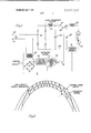
15 Claims, 9 Drawing Figures H/Gl-fiff/VCY 32 IPIFZWZ/VCI (WM was Hut/M)? SOLID STATE CHOPPER BALLAST FOR GASEOUS DISCHARGE LAMPS BACKGROUND OF THE INVENTION This invention relates to a solid state ballast circuit for gaseous discharge lamps, and more particularly to a high frequency chopper ballast for mercury vapor lamps which utilizes electronic techniques to shape the line current for high power factor and to obtain good regulation.
The majority of mercury lamps presently in use employ electromagnetic ballasts with bulky low frequency transformers, inductors and large power factor correcting capacitors. Although a number of circuits using solid state devices have been developed for ballasting high intensity discharge mercury lamps and similar lamps, those circuits which operate on 60 Hz alternating-current or full wave rectified voltage incorporate bulky and expensive components. More sophisticated high frequency circuit approaches do not achieve an economic solution to the problem and ignore some of the major problem areas such as acoustic resonance effects and electrode degradation clue to arc initiation.
The combination of features an electronic ballast desirably should have are to provide high power factor, high efficiency, low acoustic and radio frequency interference noise, and good regulation in a single phase circuit without requiring heavy power frequency magnetics and large correction and energy storage capacitors. Further, the ballast circuit should be relatively insensitive to normal line transients, the lamp should not extinguish upon rapid excursion to 65 percent of rated line voltage, lamp operation should avoid visible flicker or acoustic resonance effects caused by continuous operation at a constant high frequency, and circuit operation should be stable for very long periods of time. The circuit should operate over an ambient temperature range of 30C to +85C and provide negligible electrical interference to its surroundings.
In the concurrently filed application Ser. No. 429,9l4 by Robert L. Steigerwald and John N. Park, entitled Power Circuits for Obtaining a High Power Factor Electronically," and assigned to the same assignee, a number of single phase chopper circuits for alternating-current and direct-current loads are described which use only high frequency filtering and electronically shape the line current to obtain a high power factor. As a typical application, a mercury lamp ballast circuit having many of the foregoing desirable features is disclosed. The present application relates to an improvement on this ballast circuit with emphasis on obtaining good lamp operation in a more satisfactory circuit configuration.
SUMMARY OF THE INVENTION The new solid state, high frequency chopper ballast is suitable for energization by unfiltered low frequency alternating-current line voltage, preferably full wave rectified with only high frequency filtering, and broadly includes a controlled switching means, such as a power transistor, and coasting device means, such as a power diode, that conduct alternately and supply lamp current through a coasting inductor to a mercury vapor lamp or other gaseous discharge lamp. A current sensor is coupled to sense the instantaneous, high frequency ripple lamp current. The control circuit has provision for generating a preselected reference signal waveshape to determine the power level, optionally regulate the lamp current, and to effect shaping of the lamp current and therefore the line current to obtain a high power factor. I By effectively comparing the sensor and reference signals, an output signal is produced for controlling the application of alternate turn-on and turnoff signals to operate the controlled switching means at a variable high frequency chopping rate to shape the lamp current as determined by the reference signal waveshape. As a result of automatic sweeping of the chopping frequency and as a result of the low ripple amplitude, acoustic resonance effects are avoided.
In accordance with the invention, an improved lamp current waveshape is obtained at initial start-up of the lamp. Also, the lamp current is improved by supplying in a more satisfactory manner a minimum lamp current in each cycle when the comparing means is ineffective to shape the lamp current, i.e., during the valleys or low voltage regions of the pulsating or sinusoidal power voltage. To avoid the undesirable glow-to-arc mode, the control circuit has provision for temporarily shaping the reference signal at initial start-up to obtain a high starting current, as by using a long time constant network to modify the action of the control function generator in the reference signal generating means. Minimum lamp current in the valley or low voltage regions for improved reignition characteristics is supplied by the high frequency filter and, in the preferred transistor d-c chopper ballast, by using local energy storage capacitors in the improved transistor drive curcuit power supply to provide base current to the normal conducting positive base drive circuit to maintain power transistor conductivity. Other control circuit improvements include a low voltage power supply for the comparator which supplies clipped, regulated voltage except during the valley regions when it is not needed, thereby eliminating the need for electrolytic capacitors. An improved transistor base drive circuit and power supply therefor are also disclosed. The new high frequency chopper ballast for mercury lamps incorporates the desirable features previously mentioned, is highly efficient with low volume and light weight, and does not employ low frequency energy storage and correction capacitors, inductors, and power transformers.
BRIEF DESCRIPTION OF THE DRAWINGS FIG. 1 is a simplified schematic circuit diagram partly in block diagram form of a d-c chopper ballast for a mercury vapor lamp and is used to explain the principles of the invention;
FIG. 2 is a waveform diagram of a sinusoidal reference signal with closely adjacent control band limits for controlling the intervals of conduction and nonconduction of the power transistor in FIG. 1;
FIG. 3 is a schematic power circuit diagram with control circuit connections according to the preferred embodiment of the mercury lamp solid state ballast circuit;
FIG. 4 shows ideal waveform diagrams of the line current and voltage, lamp current, and reference signal for the preferred ballast circuit;
FIG. 5 is an enlarged diagram of the flattened sinusoidal reference signal and control band limits for the control circuit logic signals;
FIG. 6 are typical oscilloscope waveforms of the lamp voltage and lamp current illustrating, at an enlarged scale, the high frequency ripple produced by operation of the chopper ballast;
FIG. 7 is a detailed control circuit schematic diagram for the mercury lamp ballast circuit;
FIG. 8 is a diagrammatic side view of a transformer with a pair of secondary windings for supplying power to the logic and power transistor base drive circuits in FIG. 7; and
FIG. 9 is a sketch of a portion of the control function generator in FIG. 7 modified to obtain auxiliary adaptive control of the mercury lamp chopper ballast, for example, in response to sensing the ambient light level.
DESCRIPTION OF THE PREFERRED EMBODIMENT The high frequency, single phase, direct current chopper circuit shown in FIG. I supplies a controlled current waveshape and controlled power to a mercury vapor lamp or other appropriate gaseous discharge lamp, and the line current is accordingly electronically shaped to obtain a high power factor. The power circuit is relatively simple and economical, and uses no bulky supply frequency transformers, inductors, or large energy storage or power factor correcting capacitors. The control circuit operates on the basis of continuously comparing the sensed lamp current with a preselected reference signal waveshape to thereby determine the high frequency switching rate of the power transistor and generate the desired lamp current waveshape. In the preferred chopper ballast of FIGS. 3-9, other desirable operating characteristics such as good regulation, a good starting current waveform, etc., are provided as will be explained.
The single phase power circuit (FIG. 1) has a pair of input terminals 20 and 21 connected, by way of illustration, to a 60 Hz, 277 volt source of alternating current, but other power frequencies and voltages can be used depending on the application. A diode bridge rectifier 22 connected to the a-c input terminals produces a full wave rectified sinusoidal voltage which is supplied essentially unfiltered to the chopper circuit. A high frequency filter provided for example by a series inductor 23 and a shunt capacitor 24 is connected across the output terminals of the bridge rectifier 22, but these high frequency filter components essentially are provided to isolate the high frequency chopping from the 60 Hz line. It may be preferable to further include a second shunt filter capacitor connected between the input lines, and other variations are possible depending upon the amount of line filtering required. In the chopper circuit, a power transistor 25 and power coasting diode 26 are connected in series between the high voltage, 120 Hz, pulsating d-c supply terminals 27 and 28, and a coasting inductor 29 is connected in series with the mercury lamp 30 across the coasting diode 26. A suitable load current sensor 31, such as a small current transformer or sensing resistor, is coupled in series with the lamp 30, and continuously supplies an input signal to the control circuit which is indicative of the magnitude of the instantaneous lamp current. In operation, in the same manner as a time ratio control circuit, the power transistor 25 is turned on and off at a high frequency switching rate. During conducting intervals of the transistor 25 power is supplied to the load 30 through the coasting inductor 29, and during nonconducting intervals of the transistor 25 the coasting diode 26 becomes forward biased and provides a path for load current as the stored energy in coasting inductor 29 discharges. The circuit is preferably operated in the tens of kilohertz frequency range, in the range of about 10 kHz to 40 kHz for this application. With this power circuit configuration, it is noted, there is inherently a small high frequency ripple in the load current.
The coasting diode 26 and power transistor 25 are preferably matched devices in order to eliminate additional power circuit components in the coasting path. In each high frequency cycle when the power transistor is rendered conductive, the coasting diode does not immediately block due to stored charges and higher than normal currents flow in the power transistor. The peak current generated during this transient is limited by employing a fast recovery coasting diode and by making a reasonably close match of the turn-on time of transistor 25 to the recovery time of the coasting diode. A controlled recovery diode is used rather than a snap off diode to prevent large transient voltages from developing across the diode and to prevent generation of high frequency disturbances.
The control circuit generates a reference signal which is basically in phase with the applied line voltage and has a predetermined waveshape and magnitude to achieve high power factor and deliver a selected amount of power to the load. As has been pointed out, in this power circuit the reference signal determines the load current waveshape and thus the line current waveshape and input power for a given lamp. The reference signal waveshape can also be selected to achieve additional desirable features such as good regulation and suitable load current waveshapes to meet the range of load operation conditions. Accordingly, the exact reference signal waveshape that is selected depends upon the combination of features that are required or the best compromise, depending upon the particular circumstances. In order to eliminate the need for special signal generating equipment such as low frequency oscillators, the control signal is derived directly from the a-c input lines and then shaped according to a selected control function to obtain the desired reference signal waveshape. The reference signal is then also in phase with the line voltage. To this end, a step-down transformer 32 is connected across the input lines and, for the power circuit configuration, feeds a diode bridge rectifier 33 so that the input to a control function generator 34 is a full wave rectified d-c voltage. Generally speaking, the control function is selected as previously described and can be a constant gain, an electronically variable gain, a squaring circuit, a square root circuit, etc., depending upon the type of load and control desired. Referring also to FIG. 2, there are closely adjacent control band limits associated with the reference signal that efi'ectively determine the limits of excursion of the lamp current as shaped by the controlled switching action of the power transistor 25. The control band is effectively placed about the reference signal, or can be entirely at one side of the reference signal or closely spaced from it. In any case, the control band limits are close to or coincide with the reference signal and conform to its waveshape. Although other circuitry can be employed to obtain the control band limits, a simple and effective implementation is by the use of a comparator 35 with hysteresis. The hysteresis characteristic may be obtained by a feedback connection from the output of the comparator to the positive input of the comparator, as is further explained with regard to FIG.
7. The reference signal is applied to the positive input of comparator 35, while the negative input is a sensor signal indicative of the instantaneous lamp current generated by the current sensor 31.
An output from the comparator 35 is amplified by amplifier 36 and is effective to apply a base drive signal to the power transistor 25 to drive it into saturation and render it conductive. Assuming that lamp current is circulating in the coasting path and is decreasing, and that there is a low output from the comparator 35 so that power transistor 25 is turned off, the lamp current continues to decrease until the current sensor signal at the negative input of the comparator is equal to and about to go below the reference signal control band limit at the positive input of the comparator (i.e., the reference signal minus hysteresis). A comparator output is now produced, turning on the power transistor 25 and causing an increase in the lamp current as current is drawn from the supply. The reference signal now switches to its upper control band limit value (i.e., the reference signal plus hysteresis), and the comparator output remains high and the power transistor 25 remains conductive until the lamp current increases and the current sensor signal becomes equal to the value of the other reference signal control band limit. The comparator output then goes low, thereby turning off the power transistor 25 and switching the value of the reference signal at the positive input of the comparator to its lower control band limit. The lamp current therefore has a small amount of ripple about the nominal value determined by the reference signal hysteresis. The chopping frequency of the circuit is not constant during each cycle of the rectified sinusoidal voltage supplied to the chopper circuit. The chopping frequency is determined primarily by the value of the coasting inductor 29, the instantaneous voltage difference between the rectified sinusoidal voltage feeding the chopper and the actual lamp voltage, the storage time of power transistor 25, and the comparator hysteresis. For the circuit shown in FIG. 1, the chopping frequency is considerably higher at the middle of the half cycle than at either end where the supply voltage is low. This periodically variable chopping frequency is desirable for some loads, for example as a factor in eliminating acoustic resonance problems in mercury vapor lamps which can occur under certain constant high frequency conditions.
Having discussed the underlying principles of the chopper circuit and control technique, the preferred embodiment of the invention will be described with regard to FIGS. 3-9. The power circuit (FIG. 3) is similar to FIG. 1 and is suitable for HID mercury lamps in the 74 to 1000 watt range and also, without modification, for other gaseous discharge lamps that are operable on unfiltered full wave rectified 120 Hz (or 100 Hz) voltage which cyclically drops to zero in the valley regions. The preferred circuit is discussed with regard to ballasting a 250 watt mercury vapor lamp, giving typical values of the voltages, currents and other parameters to clarify the presentation. When appropriately modified, the ballast circuit may be used with still different types of gaseous discharge lamps that require a supply of lamp current in the valleys to maintain sufficient lamp ionization until the 120 Hz wave rises to a usable level. Within the broader scope of the invention, the chopper ballast can be constructed in a-c versions without a full wave rectifier using a pair of inverse-parallel power switches and coasting devices to provide bidirectional conducting capability. This is further explained in the aforementioned concurrently filed application Ser. No. 429,914, to which the reader may refer for further information. lnstead of the power transistor, a gate turnoff thyristor can be used, both of these being described generically as a controlled solid state switch with a single electrode for turn-on and turnoff. The power circuit is preferably fabricated by power module techniques while the control curcuit is fabricated using integrated circuit and microelectronic techniques.
In FIG. 3, high frequency filtering and transient voltage protection is provided at the input to the chopper circuit and is effective as to both the power circuit and the control circuit. The input high frequency filter serves primarily to limit the amount of radio frequency interference which appears across the line due to the operation of the chopper, and includes a second shunt capacitor 24' as well as the series filter inductor 23 which now has a small parallel resistor 40 to prevent ringing in the filter circuit due to transient excitation. The filter inductor also provides sufficient series impedance to permit effective line transient voltage sup pression for all the power and control circuit components by means of a single polycrystalline varistor 41 effectively connected between the input terminals of diode bridge rectifier 22. The input voltage for the control circuit 42 is taken between these same two lines. By way of example, varistor 4] is a GE-MOV varistor (trademark of the General Electric Company), type V275LA20. The high frequency filter also includes the shunt capacitor 24 (now provided with a parallel bleeder resistor 43) to provide a circulating path for the high frequency current components of the transistor chopper circuit. Thus, the voltage feeding the chopper is essentially a full wave rectified Hz line voltage.
The power transistor 25, for instance, is a Toshiba ZSCl 172A transistor and a suitable matched coasting diode 26 is a MR856 power diode manufactured by Motorola, lnc. The current sensor is a small sensing resistor 31', such as a one-half ohm resistor, connected in series with coasting inductor 29 and mercury lamp 30, the coasting diode 26 being connected across all these elements. The voltage across the sensing resistor 31 is supplied to the control circuit 42 and is indicative of the instantaneous lamp current. This is a negativegoing signal voltage in this circuit arrangement. The input voltage derived from the line supplies power to the control circuit 42 and also provides a control signal that is modified by the selected control function to provide the reference signals. The control circuit 42 further includes dual base drive circuitry for the power transistor 25 which is effective to turn on, hold on, positively turn off, and hold off the power transistor. The base drive current and voltage supplied by control circuit 42 provides the proper conditions for chopper operation with a full wave rectified supply voltage. As will be further explained, the base current is proportional to the collector current in the power transistor, and electrolytic capacitors are not needed in the base drive circuitry, nor also in the control function generator and comparator circuitry.
Referring to the waveform diagrams in FIG. 4, it is realized in practice that the line voltage varies under normal conditions. The reference signal e is a full wave rectified, flattened sinusoidal signal, and the control function additionally provides an electronically variable gain characteristic so that the lamp current remains approximately constant despite line voltage variations. This provides good lamp current regulation for a reasonable range of line voltage variations. A mercury lamp load is a non-linear load with a negative resistance characteristic at low frequencies, and further has some of the characteristics of a back emf load. There is some lamp current at the beginning of each cycle before ignition and at the end of each cycle, when the line voltage is low. To further explain the concept of the back emf load, if it is assumed that the load is a battery being charged, it is readily seen that power is transferred to the battery only in those portions of the cycle when the instantaneous applied voltage is greater than the battery voltage. For instance, for a battery of I volts and a peak full wave rectified sinusoidal voltage of 400 volts, no power is transferred to the battery at the beginning and end of the cycle when the instantaneous voltage is below I00 volts. The lamp voltage between the terminals of ordinary mercury vapor lamps is typically about I30 volts. It will be further understood that there is an impedance transformation by virtue of the operation of the chopper circuit, so that the lamp current and the line current do not necessarily have the same waveshape or magnitude. From the foregoing example, it is seen that there is a voltage transformation, and in like manner, there is also a current transformation. Based on the foregoing analysis, there is some lamp current at the beginning and end of each cycle when the supply voltage is low, and in the inter mediate portion of each cycle the lamp current is forced to follow the flattened sinusoidal reference signal. The shaped line current draws increased current due to ignition of the lamp near the beginning of the cycle, but can be described as being roughly constant in the intermediate portion of each cycle, dropping at the end of the cycle in the valley regions of the rectified supply voltage. This line current waveshape is in phase with the line voltage and provides high power factor, easily in excess of 90 percent, with good regulation of the lamp current and input power.
The flattened and regulated sinusoidal reference signal is actually negative-going as shown in FIG. 5. The lamp current has a high frequency ripple about a nominal value, and in the reproductions of typical oscilloscope waveforms of the lamp current given in FIG. 6, the ripple in the shaped, flattened sinusoidal lamp current is illustrated diagrammatically at enlarged scale. The lamp voltage waveform also exhibits a high frequency ripple and shows the momentarily higher voltage drawn at reignition at the beginning of each cycle. In the valleys of the full wave rectified supply voltage, the lamp plasma actually deionizes to a certain extent, such that it can be said that the lamp reignites in each cycle. The minimum lamp current in the valleys maintains sufficient ionization for good reignition characteristics. For a 277 volt to 208 volt source, either 60 Hz or 50 Hz, the supply voltage rises to a sufficiently high level near the beginning of a cycle to permit reignition.
FIG. 7 is a detailed schematic circuit diagram of the improved control circuit 42. The step-down transformer 45 is energized by the high frequency filtered, varistor-protected line voltage and has a pair of centertapped secondary windings, one of which supplies low voltage, high current power (typically l2 volts peak, I amp peak) for the dual base drive circuitry of power transistor 25, while the other pair of center-tapped secondary windings supplies high voltage, low current power (typically volts peak, 30 milliamps peak) for the logic portions of the control circuit. A suitable transformer construction that provides a low capacitance between the primary winding and each secondary winding is shown in FIG. 8. The bobbin 47 is disposed about the central leg of the magnetic core 48. Bobbin 47 has a multiple wall structure that provides a series of axially spaced compartments for the winding of the separate transformer windings in the axial sequence of S1, S3, P, S4, and S2. The secondary winding designations correspond to those in FIG. 7. This low capacitance wafer wound design is effective to prevent the coupling of high frequency current components between the secondary windings and between the secondary and primary windings, i.e., it provides a low rfi coupling. The centertapped secondary windings S1 and S2 (FIG. 7) are connected to a first full wave diode bridge rectifier 49 and generates a positive-going rectified sinusoidal voltage at one output junction 50 and a negative-going rectified sinusoidal voltage at the other output junction 51. This negative rectified sinusoidal voltage, with a typical peak value of about 50 volts, is fed to the control function generator 34 which produces the flattened sinusoidal, automatic gain controlled reference signal.
An additional important function of the peak detector circuit 61 for controlling the gate voltage of FET 59 is to provide an improved starting current waveform for the lamp to minimize electrode degradation during arc initiation. The time constant of the series RC network (primarily resistor 64 and the capacitor) is relatively long and is effective to delay the divider action a few seconds. That is, the capacitor at the gate of FET 59 charges slowly upon exciting the ballast circuit, with the result that the FET resistance is initially high as is the value of the generated reference voltage. The starting lamp current therefore is momentarily relatively high to quickly heat the cathode and avoid the undesirable glow-to-arc mode. By way of illustration, for a 250 watt mercury lamp, the starting current ramps from amps peak to the normal 3 amps peak in approximately 8 seconds. Also, it is possible to provide the circuit with sophisticated adaptive control by controlling the voltage at the gate of FET 59. For example, referring to FIG. 9, the ambient light level may be sensed by a phototransistor 65 or other photosemiconductor and used to actuate an auxiliary adaptive control circuit 66 which in turn can determine the voltage at the gate of the field effect transistor and consequently the magnitude of the reference voltage. Alternatively, the output from the adaptive control circuit can be connected directly to a comparator input. In this manner, a lamp can automatically be turned on and off in response to the ambient light level, or timing circuits may be employed to control the power level of operation over any given time duration, and there are other possibilities. Adaptive control circuit 66 can be employed to control the power delivered to the lamp. That is, by sensing the lamp voltage as well as the lamp current, the sensed lamp voltage is used to control the output of auxiliary adaptive control circuit 66. The reference signal is then modified by control of the gate voltage of PET 59 to keep the lamp power approximately constant.
The comparator 35 is preferably an integrated circuit component such as the LM-3ll device manufactured by the National Semiconductor Corp. A positive low voltage power supply and a negative low voltage power supply produces the respective voltages +V,, and V,,, for supplying power to the comparator. These power supplies are produced by clipping the high positive and negative voltages at the outputs of bridge rectifier 49, and obviate the need for electrolytic capacitors. Although there is no power for comparator 35 during the valleys of the full wave rectified 120 Hz voltage, power is not needed at these times since lamp current during the valley regions is not determined by action of the comparator. Some lamp current is provided by another mechanism, as will be explained. The positive low voltage power supply is comprised by a resistor 67 and a small Zener diode 68 conneceted in series between the bridge output junction 50 and the center-tap between the secondary transformer windings SI and S2, and a transistor 69 having its collector-base connected across the resistor 67 while the emitter is connected to the appropriate pins in comparator 35. This is recognized as being a series pass transistor regulator. As the voltage at point 5. rises, current is supplied through resistor 67 to Zener diode 68 and to the baseemitter junction of transistor 69. After the Zener diode clamps the base voltage, the circuit functions as a series voltage regulator with the voltage at the emitter of transistor 69 being approximately +5 volts. The negative low voltage power supply at the other side of bridge rectifier 49 is similar with corresponding components designated by corresponding primed numerals. In addition, it is noted that a high frequency filter capacitor 70 is connected between the junction of resistors 53'and 54 and the common bus 52 to filter undesirable high frequency transients in the control voltage. Also, to provide filtering of the comparator power supply, small capacitors 71 and 71 are respectively connected between the +V and buses and the common bus 52.
The minus terminal of sensing resistor 31 as previously mentioned, is coupled to the negative input of comparator 35, while the plus terminal is referenced to the center-tap between the pair of secondary windings S1 and S2 of transformer 45, which is the common point. To eliminate fast switching transients which could give a false peak lamp current identification, an RC filter comprised by resistor 72 and capacitor 73 is effectively connected across the sensing resistor. The positive input is connected through a resistor 74 to the junction of resistors 55 and 56 at which the flattened sinusoidal reference signal is generated. To provide a comparator hysteresis characteristic, a relatively large resistor 75 is connected in a feedback path between the output and the positive input of the comparator, and functions with resistor 74 as a voltage divider. The amount of feedback voltage or feedback current at the positive input has two values depending upon whether the comparator output is high or low. The net instantaneous voltage at the positive input is thus determined by the instantaneous value of the negative-going flattened sinusoidal reference signal and by the amount of feedback voltage. As a result of the normal operation of the chopper circuit, as previously explained, the changing current sensor signal in the logic circuit at the negative input of the comparator is alternately compared with the two reference signal control band limits. This will be reviewed again later.
The output of comparator 35, which typically has a low output of 5 volts and a high output of +5 volts, is coupled to an output transistor 76 which provides the interface between the logic circuit and the power transistor drive circuit. In particular, the comparator output is connected to the junction of a pair of resistors 77 and 78 that are connected between the base and an emitter resistor 93 for transistor 76, the resistor 93 further being connected to the V,,,. bus. Upon the occurrence of a high comparator output, current is supplied to transistor 76 thereby rendering it conductive. The net effect of this action, it will be recalled, is to turn off the power transistor 25.
Relatively low voltage, high current, full wave rectified 120 Hz unidirectional voltage is supplied to the power transistor base drive circuit by means of a sec- 0nd diode bridge rectifier 80 that is energized by the second pair of secondary windings S3 and S4 of transformer 45. A pair of relatively small, local energy storage capacitors 81 and 82 are respectively coupled between the center-tap of the transformers secondary windings S3 and S4 and the positive and negative d-c supply terminals 83 and 84 of bridge rectifier 80. In each cycle, these capacitors store energy which is available for discharge in the valley regions of the rectified 120 Hz wave, thereby providing a source of base current for the power transistor 25 in the valley regions when the control logic does not function. These capacitors also provide low impedance sources so that fast rising current waves can be developed to properly drive power transistor 25. The power transistor base drive circuitry is divided into alternately operating positive and negative base drive circuits 85 and 86 that serve to turn on, hold on, positively turn off, and hold off the power transistor 25. The magnitude of the positive base current varies as a chopped half sinusoid since only high frequency filtering is provided by the capacitors 81 and 82, and therefore the collector current in power transistor 25 is proportional to the base current in transistor 25. Thus, the peak base current (I amp) is supplied only when it is absolutely needed at the point of highest collector current, while at other times base current is reduced, thereby obtaining high efficiency. in the positive base drive circuit 85, the collectors of a pair of transistors in a Darlington amplifier 87 are connected through a pair of parallel resistors 88 to the positive bridge output terminal 83, while the emitter of the Darlington amplifier is coupled to the base electrode 89 of the power transistor. The base of the first transistor is coupled through a biasing resistor 90 to the terminal 83, with the result that the transistor Darlington amplifier 87 is normally conducting and supplies base current to the base electrode 89. The negative base drive circuit includes a second Darlington amplifier 91 comprised by a pair of opposite type transistors whose emitter and collector are respectively connected together and tied to the base electrode 89. The emitter of the Darlington amplifier 91 is coupled through a resistor 92 to the negative bridge supply terminal 84, and the base of the Darlington amplifier is coupled directly to the collector of the transistor 76 and is also coupled directly to the base of the other Darlington amplifier 87. With this arrangement, a positive output from comparator 35 turns on the transistor 76, which is effective in turn to turn off the Darlington amplifier 87 in the positive base drive circuit while simultaneously rendering conductive the Darlington amplifier 91 in the negative base drive circuit. Excitation of the negative base drive circuit 86, of course, renders the power transistor 25 nonconductive. Upon application of the negative base drive current to the base electrode, stored charge in the base of power transistor 25 is extracted and it turns off. During the remainder of the off-time, transistor 76 remains conductive since there is current through resistor 90, and the small negative voltage at the junction of resistor 90 and the collector of transistor 76, to which the base of Darlington amplifier 91 is connected, is effective to maintain the conductivity of Darlington amplifier 91 and apply a negative bias to the base electrode 89 which positively holds off the power transistor 25. With this arrangement, clamping diodes between the base and emitter of the power transistor 25 are not needed since base electrode 89 is effectively clamped to the V,,, supply through transistor 76 and resistor 93. In the valley regions of the pulsating 120 Hz unidirectional voltage, the local energy storage capacitor 81 discharges to provide a small amount of current through resistors 88 and 90 and Darlington amplifier 87 to maintain the conductivity of power transistor 25 in the valley regions. The value of high frequency filter capacitor 24 in the power circuit as shown in FIG. 3 is sufficiently large (such as 3 microfarads for the circuit being described) to maintain some lamp current in the valleys of the energizing power voltage, a condition which is desirable for good reignition characteristics.
The operation of the solid state mercury lamp chopper ballast will be reviewed only briefly with reference to FIGS. 3-7. Since only high frequency filtering ofthe line voltage is provided in the power circuit, the voltage supplied to the transistor chopper circuit is essentially a pulsating, full wave rectified, 120 Hz sinusoidal volt age, The line voltage is also supplied by means of stepdown transformer 45 to the control circuit 42. In the control circuit (FIG. 7), the negative full wave rectified, relatively high voltage, low current (50 volts, 30 milliamperes) sinusoidal voltage at the output junction 51 of bridge rectifier 49 is used as a control voltage for the control function generator 34. In this sub-circuit. a voltage divider comprised by resistors 53-56 has a variable resistance component provided by FET 59, the channel of which is connected in series with variable resistor 60 across the resistor 56. The automatic gain control feature is obtained since the gate voltage as determined by the peak detector 61 is proportional to the peak of the rectified control voltage. When the magnitude of this voltage drops, for example, FET 59 tends to turn off and increases the variable resistance in the voltage divider so that the reference signal taken at the junction between resistors 55 and 56 remains approximately constant with line voltage variations. The sinusoidal control voltage is further flattened somewhat by means of a small current drain through the resistor 57 and Zener diode 58. The regulated, flattened sinusoidal reference signal supplied to the positive input of comparator 35 results in good lamp current regulation and a slight reduction in the peak current which the power transistor 25 conducts (as compared to the unflattened sinusoidal case).
Upon energizing the ballast circuit, the positive base drive circuit automatically conducts and supplies base current to the power transistor 25, thus applying line voltage to the lamp. For a 208-277 line, the peak voltage is sufficient to start a mercury lamp. The starting lamp current is momentarily relatively high because the reference signal is initially high due to the long RC circuit time constant of the resistor 64 and the resistor and capacitor in peak detector circuit 61. The high starting current quickly heats the cathode of the lamp to avoid the undesirable glow-to-arc mode, and the current typically ramps down from a 5 amps peak to the normal 3 amps peak in about 8 seconds. The buildup in lamp current is sensed by the sensing resistor 31' and supplied as a negative-going sensor signal to the negative input of comparator 35. The RC filter 72, 73 prevents fast switching transients from giving a false peak lamp current signal. Assuming that the line voltage is high enough to cause ignition of the mercury lamp (see FIGS. 4 and 6), the lamp current is thereafter shaped in accordance with the flattened sinusoidal reference voltage until near the end of the cycle in the valley region of the pulsating I20 Hz d-c voltage. In the steady state, the base current of the power transistor 25 is at all times proportional to the collector current whose envelope varies approximately as half sinusoid. It will be recalled that the comparator 35 has a hysteresis characteristic and that there is a polarity inversion since the reference signal is negative-going while the lamp current is positive. Assuming that power transistor 25 is conducting and the lamp current is increasing, with a low output from comparator 35, the lamp current increases until the current sensor signal is equal to the reference signal control band limit corresponding to maximum current (see FIG. 5). The output of comparator 35 new changes to the high output and renders conductive the transistor 76, which is the interface between the logic circuitry and the power transistor base drive circuit, thereby causing the negative base drive circuit 86 to conduct while simultaneously turning off the positive base drive circuit 85. Power transistor 25 is now nonconductive. and load current now circulates through the coasting path provided by the forward biased power diode 26 and begins to decrease. in the meantime, the amount of feedback voltage from the output of comparator 35 to the positive input has changed, thereby switching the basis for comparison to the other reference signal control band limit corresponding to the minimum current value. As previously explained, power transistor turns off before the end of the high frequency cycle and is held in the nonconducting condition by the fact that transistor 76 and Darlington amplifier 91 remain conducting to apply a negative potential to the base electrode 89 of power transistor 25. When the decreasing current sensor sig nal becomes equal to the other control band limit, the output of comparator 35 goes low, thereby turning off the interface transistor 76 and the negative base drive circuit 86 while rendering conductive the positive base drive circuit 85.
Primarily because the rate of rise of load current is variable since it is determined primarily by the difference between the instantaneous sinusoidal supply voltage (about 400 volts peak) and the lamp voltage (about 130 volts constant, except for the rapid increase and decrease at ignition), the switching frequency of power transistor 25 automatically varies from approximately lO kHz to kHz and back to 10 kHz over a complete cycle. in a mercury lamp ballast, this sweeping of frequency, which occurs automatically and is inherent in the operation of the circuit, helps eliminate acoustic resonance problems. As was previously explained, the other pair of center-tapped secondary windings S3 and S4 of transformer 45 supplies, via the second bridge rectifier 80, relatively low voltage, high current (l2 volts peak, 1 amp peak). full wave rectified, pulsating 120 Hz unidirectional voltage to the transistor base drive circuit. in the valley regions when the power circuit supply voltage goes low, the comparator and associated control logic does not function, and the local energy storage capacitor 81 discharges to supply base current through the resistors 88 and 90 and Darlington amplifier 87 to the base electrode 89 of power transistor 25. This maintenance of lamp current in the valley regions is desirable for good lamp maintenance. The positive and negative low voltage power supply for comparator 35, provided by the series pass transistor regulators including elements 67-69 and (ST-69', does not function and thus the comparator does not function in the valley regions when the control voltage provided by bridge rectifier 49 goes low, however this makes no difference since the power voltage is low and the power transistor is maintained in the conducting condition.
By shaping and forcing the lamp current to a flattcned sinusoidal waveshape as shown in FIG. 4, the line current is in phase with the line voltage and is electronically shaped to obtain a high power factor exceeding 90 percent. By properly selecting the magnitude of the ref erence signal according to the power level desired and by using a control function to obtain an electronically variable gain, lamp current is regulated for a nominal line voltage of 277 volts to less than one-half percent for a plus or minus 10 percent line voltage variation. The magnitude of the high frequency ripple in the lamp current (see FIG. 6) is preselected and can be variable. and for this circuit has approximately 0.25 ampere ripple about the nominal value. The basic chopper thus can be used for mercury vapor lamps having different wattage values by properly tailoring the resistors 88 and 92 in the base drive circuitry, changing the value of sensing resistor 31, and by adjusting the values of the appropriate resistors in control function generator 34 to change the magnitude of the reference signal according to the size of the lamp being powered. With this solid state ballast circuit, lamp operation is sustained down to percent of rated line voltage. Other advantages previously mentioned are that the chopping frequency is automatically variable to help avoid acoustic resonance effects and lamp flicker.
By sustaining a minimum lamp current in the valley regions of the 120 Hz lamp current waveform, the resulting lamp voltage waveform is more suitable for lamp reignition in each cycle and promotes prolonged lamp life. The provision of a momentarily high starting current for the mercury lamp minimizes electrode degradation during arc initiation and eliminates the undesirable cathode glow-to-arc mode. The glowto-arc mode puts a high voltage and high current on the cathode. The chopper ballast operates over a 30C to +C ambient temperature range. In this regard, and of importance to the potential commercial attractiveness of the ballast, is the fact that the high frequency circuit operation is achieved with minimum capacitive energy storage so as to eliminate electrolytic capacitance and their associated problems. Furthermore, this circuit operates reliably under either short circuit or open circuit lamp load conditions. In the event that a short circuit in the lamp occurs, the circuit operates inherently to keep the current in power transistor 25 within its control limits, and in the event of an open circuit, voltage is continuously applied to the lamp terminals so that the circuit restarts automatically, assuming that the mercury lamp is cold or has cooled down enough so that it will restart immediately.
In summary, an improved chopper ballast is particularly suitable for operation of mercury vapor lamps from commercially available 60 Hz single phase line voltage in an advantageous transistor d-c chopper configuration that eliminates the need for bulky transformers, inductors, large correction and energy storage capacitors, undesirable electrolytic capacitors, and power frequency filtering. in addition to the fundamental requirement of high power factor and good regulation, the circuit supplies a lamp current waveshape especially suited for mercury and other gaseous discharge lamps operated on high frequency ripple current, with provision for a good starting current waveform, automatic sweeping of the chopping frequency to eliminate acoustic resonance problems, and a minimum lamp current in the valley regions of the pulsating energizing voltage for improved reignition. The new chopper ballast is economical, light-weight, has low volume, and can be built with state-of-the-art solid state devices.
While the invention has been particularly shown and described with reference to a preferred embodiment thereof, it will be understood by those skilled in the art that the foregoing and other changes in form and detail may be made therein without departing from the spirit and scope of the invention.
What is claimed is:
l, A solid state ballast circuit for gaseous discharge lamps comprising a solid state chopper circuit for energization by low frequency alternating-current line voltage and line current and including high frequency filter means for supplying sinusoidal power voltage between a pair of supply terminals and controlled switching means and coasting device means effectively cou pled to said supply terminals and coasting inductor means to be conductive alternately to supply lamp current through said coasting inductor means to a gaseous discharge lamp,
current sensor means coupled to sense the instantaneous lamp current and produce a sensor signal indicative thereof,
a control circuit comprising generating means for generating a reference signal with a preselected waveshape and magnitude to determine the power level and to effect shaping of said lamp current and therefore the line current to obtain a high power factor, comparing means for effectively comparing said sensor and reference signals and producing an output signal, and means actuated by said output signal for supplying turn-on and turn-off signals to operate said controlled switching means at a variable high frequency chopping rate and shape said lamp current as determined by said reference sig nal,
said control circuit further comprising means for temporarily shaping and increasing the magnitude of said reference signal at start-up to obtain a high starting lamp current, and
said control and chopper circuits further comprising means for supplying minimum lamp current for good reignition characteristics during the low voltage regions of said line voltage in each cycle when said comparing means is ineffective to shape the lamp current.
2. A solid state ballast according to claim 1 additionally including an adaptive control circuit connected with said generating means to further shape said reference signal according to a selected control.
3. A solid state ballast according to claim I wherein said generating means is comprised by a transformer energized by the low frequency line voltage for deriving a control voltage, and control function generator means for regulating and shaping said control voltage according to a predetermined control function to produce said reference signal,
said control function generator means further including said means for temporarily shaping said reference signal at start-up to obtain a high starting lamp current.
4. A solid state ballast according to claim 3 wherein said comparing means includes a comparator with hysteresis, and said comparator has a series pass transistor regulator low voltage power supply energized by said transformer which supplies regulated clipped voltage to said comparator except during the low voltage regions of the line voltage.
5. A solid state ballast according to claim 1 wherein said generating means is comprised by means energized by the low frequency line voltage for deriving a control voltage in phase with the line voltage, and control function generator means for shaping said control voltage according to a predetermined control function to produce said reference signal,
said control function generator means further including said means for temporarily shaping said reference signal at start-up to obtain the high starting lamp current.
6. A solid state ballast according to claim 5 wherein said means for temporarily shaping said reference sigmil at start-up is provided by a long time constant resistor-capacitor network for temporarily modifying operation of said control function generator means.
7. A solid state ballast according to claim 6 wherein said comparing means includes a comparator with hysteresis, and said comparator has low voltage power supply means energized by said means for deriving a control voltage which supplies regulated voltage to said comparator except during the low voltage regions of the line voltage.
8. A solid state ballast circuit for gaseous discharge lamps comprising a solid state chopper circuit for energization by low frequency alternating-current line voltage and line current and including full wave rectifying means and high frequency filter means for supplying rectified sinusoidal power voltage between a pair of unidirectional voltage supply terminals, and further including a power transistor and coasting diode connected in series between said supply terminals that conduct alternately and supply lamp current through a coasting inductor and gaseous discharge lamp that in turn are connected in series across said coasting diode,
current sensor means coupled to sense the instantaneous lamp current and produce an instantaneous sensor signal indicative thereof,
a control circuit comprising a transformer and a first bridge rectifier energized by the low frequency line voltage for generating full wave rectified sinusoidal control voltage, a control function generator circuit for shaping said control voltage and generating a symmetrically curved reference signal with a waveshape and magnitude selected to determine the power level and to effect shaping of the lamp current and therefore the line current to obtain a high power factor in excess of percent. a comparator circuit with hysteresis for eflectively comparing said sensor and reference signals and producing an output signal, a second bridge rectifier connected to said transformer for deriving full wave rectified sinusoidal base drive power supply voltage, a positive and negative base drive circuit connected to said second bridge rectifier for supplying alternate turn-on and turn-off signals to said power transistor with a base current proportional to collector current, and means for coupling said comparator output signal to energize said negative base drive circuit and de-energize said positive base drive circuit to thereby operate said power transistor at a variable high frequency chopping rate and effect shaping of the lamp current as determined by said reference signal waveshape,
said control circuit further comprising means for temporarily shaping and increasing the magnitude of said reference signal at start-up to obtain a high starting lamp current, and
said control and chopper circuits further comprising means for supplying minimum lamp current for good reignition characteristics during the valleys of the rectified sinusoidal power voltage when said comparator circuit is ineffective to shape the lamp current.
9. A solid state ballast according to claim 8 wherein said comparator circuit has a low voltage power supply circuit energized by said transformer that is operative to clip the full wave rectified control voltage at a selected low voltage level and supply power to said comparator circuit except during the valleys of the rectified sinusoidal power voltage.
10. A solid state ballast according to claim 8 wherein said chopper circuit has a pair of input terminals and said high frequency filter means includes a shunt capacitor and series inductor connected between said input terminals and full wave rectifying means, and a polycrystalline varistor connected between the input terminals of said full wave rectifying means, said transformer likewise having a primary winding connected between the input terminals of said full wave rectifying means, to thereby provide filtering and protection for both the control circuit and chopper circuit.
1 l. A solid state ballast according to claim 8 wherein said comparator circuit has at least one series pass transistor regulator low voltage power supply circuit energized by said transformer that is operative to clip the full wave rectified control voltage at a selected low voltage level and supply power to said comparator circuit except during the valleys of the rectified sinusoidal power voltage.
12. A solid state ballast according to claim 8 wherein said control function generator circuit is comprised by a resistive voltage divider circuit having a variable resistance branch including and controlled by an insulated-gate field effect transistor, and
said means for temporarily shaping said reference signal at start-up to obtain a high starting lamp current is provided by a long time constant resistorcapacitor network connected to the gate of said field effect transistor for temporarily determining the gate voltage and therefore the resistance of said field effect transistor. 1
13. A solid state ballast according to claim 8 wherein said control function generator circuit is comprised by a resistive voltage divider circuit having a variable resistance branch including and controlled by an insulated-gate field effect transistor. and further comprises a control voltage peak detector circuit connected to the gate of said field effect transistor for determining the gate voltage and therefore the resistance of said field effect transistor to thereby provide automatic gain control of said reference signal to regulate the lamp current,
said peak detector circuit having a long time constant to thereby provide said means for temporarily shaping said reference signal at start-up to obtain a high starting lamp current.
14. A solid state ballast according to claim 8 wherein said positive base drive circuit is connected to said second bridge rectifier to be normally conductive in the absence of said comparator output signal, and
said means for supplying minimum lamp current during the valleys of the rectified sinusoidal power voltage includes local energy storage capacitors coupled to said second bridge rectifier and to a reference point that discharge to provide base current to maintain conductivity of said power transistor during the power voltage valleys, said high freguency filter means including a filter capacitor connected between said unidirectional voltage supply terminals which supplies lamp current during the power voltage valleys.
15. A solid state ballast according to claim 8 wherein said control function generator circuit is comprised by a resistive voltage divider circuit having a variable resistance branch including an insulated-gate field effect transistor, and
an adaptive control circuit connected to the gate of said field effect transistor to determine the gate voltage and therefore the resistance of said field effect transistor to further shape said reference signal according to a selected control.
Claims (15)
1. A solid state ballast circuit for gaseous discharge lamps comprising a solid state chopper circuit for energization by low frequency alternating-current line voltage anD line current and including high frequency filter means for supplying sinusoidal power voltage between a pair of supply terminals and controlled switching means and coasting device means effectively coupled to said supply terminals and coasting inductor means to be conductive alternately to supply lamp current through said coasting inductor means to a gaseous discharge lamp, current sensor means coupled to sense the instantaneous lamp current and produce a sensor signal indicative thereof, a control circuit comprising generating means for generating a reference signal with a preselected waveshape and magnitude to determine the power level and to effect shaping of said lamp current and therefore the line current to obtain a high power factor, comparing means for effectively comparing said sensor and reference signals and producing an output signal, and means actuated by said output signal for supplying turn-on and turnoff signals to operate said controlled switching means at a variable high frequency chopping rate and shape said lamp current as determined by said reference signal, said control circuit further comprising means for temporarily shaping and increasing the magnitude of said reference signal at start-up to obtain a high starting lamp current, and said control and chopper circuits further comprising means for supplying minimum lamp current for good reignition characteristics during the low voltage regions of said line voltage in each cycle when said comparing means is ineffective to shape the lamp current.
2. A solid state ballast according to claim 1 additionally including an adaptive control circuit connected with said generating means to further shape said reference signal according to a selected control.
3. A solid state ballast according to claim 1 wherein said generating means is comprised by a transformer energized by the low frequency line voltage for deriving a control voltage, and control function generator means for regulating and shaping said control voltage according to a predetermined control function to produce said reference signal, said control function generator means further including said means for temporarily shaping said reference signal at start-up to obtain a high starting lamp current.
4. A solid state ballast according to claim 3 wherein said comparing means includes a comparator with hysteresis, and said comparator has a series pass transistor regulator low voltage power supply energized by said transformer which supplies regulated clipped voltage to said comparator except during the low voltage regions of the line voltage.
5. A solid state ballast according to claim 1 wherein said generating means is comprised by means energized by the low frequency line voltage for deriving a control voltage in phase with the line voltage, and control function generator means for shaping said control voltage according to a predetermined control function to produce said reference signal, said control function generator means further including said means for temporarily shaping said reference signal at start-up to obtain the high starting lamp current.
6. A solid state ballast according to claim 5 wherein said means for temporarily shaping said reference signal at start-up is provided by a long time constant resistor-capacitor network for temporarily modifying operation of said control function generator means.
7. A solid state ballast according to claim 6 wherein said comparing means includes a comparator with hysteresis, and said comparator has low voltage power supply means energized by said means for deriving a control voltage which supplies regulated voltage to said comparator except during the low voltage regions of the line voltage.
8. A solid state ballast circuit for gaseous discharge lamps comprising a solid state chopper circuit for energization by low frequency alternating-current line voltage and line current and including full wave rectifying means and high frequenCy filter means for supplying rectified sinusoidal power voltage between a pair of unidirectional voltage supply terminals, and further including a power transistor and coasting diode connected in series between said supply terminals that conduct alternately and supply lamp current through a coasting inductor and gaseous discharge lamp that in turn are connected in series across said coasting diode, current sensor means coupled to sense the instantaneous lamp current and produce an instantaneous sensor signal indicative thereof, a control circuit comprising a transformer and a first bridge rectifier energized by the low frequency line voltage for generating full wave rectified sinusoidal control voltage, a control function generator circuit for shaping said control voltage and generating a symmetrically curved reference signal with a waveshape and magnitude selected to determine the power level and to effect shaping of the lamp current and therefore the line current to obtain a high power factor in excess of 90 percent, a comparator circuit with hysteresis for effectively comparing said sensor and reference signals and producing an output signal, a second bridge rectifier connected to said transformer for deriving full wave rectified sinusoidal base drive power supply voltage, a positive and negative base drive circuit connected to said second bridge rectifier for supplying alternate turn-on and turn-off signals to said power transistor with a base current proportional to collector current, and means for coupling said comparator output signal to energize said negative base drive circuit and de-energize said positive base drive circuit to thereby operate said power transistor at a variable high frequency chopping rate and effect shaping of the lamp current as determined by said reference signal waveshape, said control circuit further comprising means for temporarily shaping and increasing the magnitude of said reference signal at start-up to obtain a high starting lamp current, and said control and chopper circuits further comprising means for supplying minimum lamp current for good reignition characteristics during the valleys of the rectified sinusoidal power voltage when said comparator circuit is ineffective to shape the lamp current.
9. A solid state ballast according to claim 8 wherein said comparator circuit has a low voltage power supply circuit energized by said transformer that is operative to clip the full wave rectified control voltage at a selected low voltage level and supply power to said comparator circuit except during the valleys of the rectified sinusoidal power voltage.
10. A solid state ballast according to claim 8 wherein said chopper circuit has a pair of input terminals and said high frequency filter means includes a shunt capacitor and series inductor connected between said input terminals and full wave rectifying means, and a polycrystalline varistor connected between the input terminals of said full wave rectifying means, said transformer likewise having a primary winding connected between the input terminals of said full wave rectifying means, to thereby provide filtering and protection for both the control circuit and chopper circuit.
11. A solid state ballast according to claim 8 wherein said comparator circuit has at least one series pass transistor regulator low voltage power supply circuit energized by said transformer that is operative to clip the full wave rectified control voltage at a selected low voltage level and supply power to said comparator circuit except during the valleys of the rectified sinusoidal power voltage.
12. A solid state ballast according to claim 8 wherein said control function generator circuit is comprised by a resistive voltage divider circuit having a variable resistance branch including and controlled by an insulated-gate field effect transistor, and said means for temporarily shaping said reference signal at start-up to obtain a high starting lamp current is providEd by a long time constant resistor-capacitor network connected to the gate of said field effect transistor for temporarily determining the gate voltage and therefore the resistance of said field effect transistor. l
13. A solid state ballast according to claim 8 wherein said control function generator circuit is comprised by a resistive voltage divider circuit having a variable resistance branch including and controlled by an insulated-gate field effect transistor, and further comprises a control voltage peak detector circuit connected to the gate of said field effect transistor for determining the gate voltage and therefore the resistance of said field effect transistor to thereby provide automatic gain control of said reference signal to regulate the lamp current, said peak detector circuit having a long time constant to thereby provide said means for temporarily shaping said reference signal at start-up to obtain a high starting lamp current.
14. A solid state ballast according to claim 8 wherein said positive base drive circuit is connected to said second bridge rectifier to be normally conductive in the absence of said comparator output signal, and said means for supplying minimum lamp current during the valleys of the rectified sinusoidal power voltage includes local energy storage capacitors coupled to said second bridge rectifier and to a reference point that discharge to provide base current to maintain conductivity of said power transistor during the power voltage valleys, said high freguency filter means including a filter capacitor connected between said unidirectional voltage supply terminals which supplies lamp current during the power voltage valleys.
15. A solid state ballast according to claim 8 wherein said control function generator circuit is comprised by a resistive voltage divider circuit having a variable resistance branch including an insulated-gate field effect transistor, and an adaptive control circuit connected to the gate of said field effect transistor to determine the gate voltage and therefore the resistance of said field effect transistor to further shape said reference signal according to a selected control.
Priority Applications (5)
| Application Number | Priority Date | Filing Date | Title |
|---|---|---|---|
| US430088A US3890537A (en) | 1974-01-02 | 1974-01-02 | Solid state chopper ballast for gaseous discharge lamps |
| CA216,294A CA1042500A (en) | 1974-01-02 | 1974-12-16 | Solid state chopper ballast for gaseous discharge lamps |
| GB54377/74A GB1496129A (en) | 1974-01-02 | 1974-12-17 | Solid state ballast for gaseous discharge lamps |
| JP49147693A JPS5098174A (en) | 1974-01-02 | 1974-12-24 | |
| DE19742461449 DE2461449A1 (en) | 1974-01-02 | 1974-12-24 | CHOPPER FRAME ARRANGEMENT FOR GAS DISCHARGE LAMPS |
Applications Claiming Priority (1)
| Application Number | Priority Date | Filing Date | Title |
|---|---|---|---|
| US430088A US3890537A (en) | 1974-01-02 | 1974-01-02 | Solid state chopper ballast for gaseous discharge lamps |
Publications (1)
| Publication Number | Publication Date |
|---|---|
| US3890537A true US3890537A (en) | 1975-06-17 |
Family
ID=23706015
Family Applications (1)
| Application Number | Title | Priority Date | Filing Date |
|---|---|---|---|
| US430088A Expired - Lifetime US3890537A (en) | 1974-01-02 | 1974-01-02 | Solid state chopper ballast for gaseous discharge lamps |
Country Status (5)
| Country | Link |
|---|---|
| US (1) | US3890537A (en) |
| JP (1) | JPS5098174A (en) |
| CA (1) | CA1042500A (en) |
| DE (1) | DE2461449A1 (en) |
| GB (1) | GB1496129A (en) |
Cited By (100)
| Publication number | Priority date | Publication date | Assignee | Title |
|---|---|---|---|---|
| US3999100A (en) * | 1975-05-19 | 1976-12-21 | Morton B. Leskin | Lamp power supply using a switching regulator and commutator |
| US4012617A (en) * | 1975-07-24 | 1977-03-15 | Litton Systems, Inc. | Power controller for microwave magnetron |
| JPS5254278A (en) * | 1975-10-28 | 1977-05-02 | Gen Electric | Solid stabilizer |
| US4039897A (en) * | 1976-03-08 | 1977-08-02 | Dragoset James E | System for controlling power applied to a gas discharge lamp |
| US4051412A (en) * | 1976-09-02 | 1977-09-27 | General Electric Company | Discharge lamp operating circuit |
| US4051411A (en) * | 1976-09-02 | 1977-09-27 | General Electric Company | Discharge lamp operating circuit |
| US4074344A (en) * | 1975-09-22 | 1978-02-14 | Gte Sylvania Incorporated | High power factor ac to dc converter circuit |
| US4092565A (en) * | 1976-11-22 | 1978-05-30 | General Electric Company | Pulse circuit for gaseous discharge lamps |
| US4132925A (en) * | 1976-06-15 | 1979-01-02 | Forest Electric Company | Direct current ballasting and starting circuitry for gaseous discharge lamps |
| US4156166A (en) * | 1976-08-18 | 1979-05-22 | Royal Industries, Inc. | Method and apparatus for saving energy |
| US4190795A (en) * | 1977-09-09 | 1980-02-26 | Coberly & Associates | Constant intensity light source |
| US4221994A (en) * | 1978-11-09 | 1980-09-09 | Demetron Research Corporation | Photo curing light source |
| US4230971A (en) * | 1978-09-07 | 1980-10-28 | Datapower, Inc. | Variable intensity control apparatus for operating a gas discharge lamp |
| US4237403A (en) * | 1979-04-16 | 1980-12-02 | Berkleonics, Inc. | Power supply for fluorescent lamp |
| US4251752A (en) * | 1979-05-07 | 1981-02-17 | Synergetics, Inc. | Solid state electronic ballast system for fluorescent lamps |
| US4254362A (en) * | 1979-07-30 | 1981-03-03 | Midland-Ross Corporation | Power factor compensating electroluminescent lamp DC/AC inverter |
| EP0055995A1 (en) * | 1981-01-07 | 1982-07-14 | Philips Patentverwaltung GmbH | Low-pressure discharge lamp starting and operating circuit using a DC source |
| EP0066927A1 (en) * | 1981-06-04 | 1982-12-15 | Philips Patentverwaltung GmbH | Method and circuit for operating a high pressure metal vapour discharge lamp |
| DE3122183A1 (en) * | 1981-06-04 | 1982-12-23 | Philips Patentverwaltung Gmbh, 2000 Hamburg | Method for operating a high-pressure metal-vapour discharge lamp and a circuit arrangement for carrying out this method |
| US4370601A (en) * | 1980-04-21 | 1983-01-25 | Matsushita Electric Industrial Co., Ltd. | High pressure discharge lamp apparatus |
| DE3231939A1 (en) * | 1981-09-11 | 1983-03-31 | N.V. Philips' Gloeilampenfabrieken, 5621 Eindhoven | CIRCUIT ARRANGEMENT FOR OPERATING A GAS AND / OR VAPOR DISCHARGE LAMP |
| US4415839A (en) * | 1981-11-23 | 1983-11-15 | Lesea Ronald A | Electronic ballast for gaseous discharge lamps |
| US4498031A (en) * | 1983-01-03 | 1985-02-05 | North American Philips Corporation | Variable frequency current control device for discharge lamps |
| US4523131A (en) * | 1982-12-10 | 1985-06-11 | Honeywell Inc. | Dimmable electronic gas discharge lamp ballast |
| US4528482A (en) * | 1983-07-20 | 1985-07-09 | Merlo Joseph C | Control of energy to fluorescent lighting |
| US4529913A (en) * | 1981-11-09 | 1985-07-16 | Precision Mecanique Labinal | Device for controlling the light intensity of a fluorescent tube fed from a D.C. voltage |
| US4535271A (en) * | 1976-07-26 | 1985-08-13 | Wide-Lite International | High frequency circuit for operating a high-intensity, gaseous discharge lamp |
| WO1987000719A1 (en) * | 1985-07-23 | 1987-01-29 | Wolf, Karl | Circuit for starting and operating at least one low-pressure or high-pressure gas discharge lamp with high-frequnency oscillations |
| US4682084A (en) * | 1985-08-28 | 1987-07-21 | Innovative Controls, Incorporated | High intensity discharge lamp self-adjusting ballast system sensitive to the radiant energy or heat of the lamp |
| US4686428A (en) * | 1985-08-28 | 1987-08-11 | Innovative Controls, Incorporated | High intensity discharge lamp self-adjusting ballast system with current limiters and a current feedback loop |
| US4723098A (en) * | 1980-10-07 | 1988-02-02 | Thomas Industries, Inc. | Electronic ballast circuit for fluorescent lamps |
| US4724361A (en) * | 1984-12-14 | 1988-02-09 | Matsushita Electric Works, Ltd. | High pressure discharge lamp |
| EP0288924A1 (en) * | 1987-04-29 | 1988-11-02 | Omega Electronics S.A. | Power supply device for a discharge lamp |
| EP0291223A1 (en) * | 1987-05-12 | 1988-11-17 | THORN EMI plc | Power supply |
| EP0296558A1 (en) * | 1987-06-26 | 1988-12-28 | Omega Electronics S.A. | Power supply device for a discharge lamp |
| US4812736A (en) * | 1985-07-06 | 1989-03-14 | U.S. Philips Corp. | Circuit arrangement for operating high-pressure gas discharge lamps |
| US4816721A (en) * | 1982-12-11 | 1989-03-28 | U.S. Philips Corp. | Circuit arrangement for operating a high-pressure gas discharge lamp |
| US4873471A (en) * | 1986-03-28 | 1989-10-10 | Thomas Industries Inc. | High frequency ballast for gaseous discharge lamps |
| US4945289A (en) * | 1986-05-23 | 1990-07-31 | Interpatents Ltd. | Electronic supply system for fluorescent tubes with electrodes |
| EP0397334A1 (en) * | 1989-04-26 | 1990-11-14 | TLG plc | A method of operating an arc discharge lamp |
| US4999547A (en) * | 1986-09-25 | 1991-03-12 | Innovative Controls, Incorporated | Ballast for high pressure sodium lamps having constant line and lamp wattage |
| US5059869A (en) * | 1986-12-02 | 1991-10-22 | U.S. Philips Corporation | Circuit arrangement for the operation of high-pressure gas discharge lamps by means of a pulsatory supply current |
| US5059867A (en) * | 1990-04-03 | 1991-10-22 | General Electric Company | Ballast circuit with improved transfer functions |
| EP0507393A2 (en) * | 1991-04-04 | 1992-10-07 | Koninklijke Philips Electronics N.V. | Circuit arrangement |
| US5313145A (en) * | 1992-08-31 | 1994-05-17 | Francis Jr Ralph M | Power supply for a gas discharge device |
| US5319286A (en) * | 1992-10-29 | 1994-06-07 | North American Philips Corporation | Ignition scheme for a high intensity discharge ballast |
| US5422545A (en) * | 1993-08-19 | 1995-06-06 | Tek-Tron Enterprises, Inc. | Closed loop feedback control circuits for gas discharge lamps |
| US5541499A (en) * | 1993-05-21 | 1996-07-30 | Merlin Gerin | Electronic trip device comprising a power supply control device |
| US5557174A (en) * | 1993-08-25 | 1996-09-17 | Tridonic Bauelemente Gmbh | Electronic ballast with dimmer and harmonics filter for supplying a load, for example a lamp |
| US5798619A (en) * | 1995-02-15 | 1998-08-25 | Vari-Lite, Inc. | Techniques for controlling remote lamp loads |
| US5942860A (en) * | 1997-09-16 | 1999-08-24 | Philips Electronics North America Corporation | Electronic ballast for a high intensity discharge lamp with automatic acoustic resonance avoidance |
| US6034490A (en) * | 1997-06-12 | 2000-03-07 | Koito Manufacturing Co., Ltd. | Lighting circuit for discharge lamp |
| US6384544B1 (en) * | 1998-06-13 | 2002-05-07 | Hatch Transformers, Inc. | High intensity discharge lamp ballast |
| US6392355B1 (en) | 2000-04-25 | 2002-05-21 | Mcnc | Closed-loop cold cathode current regulator |
| US20030090215A1 (en) * | 2001-11-14 | 2003-05-15 | Delta Power Supply, Inc. | Lamp ignition |
| US20030098659A1 (en) * | 2001-11-26 | 2003-05-29 | Ushiodenki Kabushiki Kaisha | Light source device |
| EP1355517A1 (en) * | 2002-04-15 | 2003-10-22 | Patent-Treuhand-Gesellschaft für elektrische Glühlampen mbH | Switched converter with acoustic switching frequency |
| US20040036422A1 (en) * | 2002-05-29 | 2004-02-26 | Fumio Maruyama | Filament lamp light quantity control method and filament lamp light quantity control unit and filament lamp light source unit |
| WO2004066675A2 (en) * | 2003-01-16 | 2004-08-05 | International Rectifier Corporation | Dimming ballast control ic with flash suppression circuit |
| EP1459282A1 (en) * | 2001-12-21 | 2004-09-22 | Koninklijke Philips Electronics N.V. | Electronic ballast with low voltage output |
| US20040199227A1 (en) * | 2001-11-29 | 2004-10-07 | Altshuler Gregory B. | Biostimulation of the oral cavity |
| US20050168158A1 (en) * | 2001-03-01 | 2005-08-04 | Palomar Medical Technologies, Inc. | Flash lamp drive circuit |
| US20050218836A1 (en) * | 2002-07-04 | 2005-10-06 | Tridonic Optoelectronics Gmbh | Current supply for luminescent diodes |
| US20050218824A1 (en) * | 2004-04-06 | 2005-10-06 | Patent-Treuhand-Gesellschaft Fur Elektrische Gluhlampen Mbh | Electronic ballast with regulating circuit and disturbance variable application |
| US20050264217A1 (en) * | 2004-06-01 | 2005-12-01 | Huston Trevor L | Controller for power protection |
| US20060066262A1 (en) * | 2004-09-30 | 2006-03-30 | Fumio Maruyama | Filament lamp light quantity control method and filament lamp light quantity control unit and filament lamp light source unit |
| US20060066260A1 (en) * | 2004-09-30 | 2006-03-30 | Fumio Maruyama | Filament lamp light quantity control method and filament lamp light quantity control unit and filament lamp light source unit |
| US20060194164A1 (en) * | 2004-12-09 | 2006-08-31 | Palomar Medical Technologies, Inc. | Oral appliance with heat transfer mechanism |
| US20070078501A1 (en) * | 2002-05-23 | 2007-04-05 | Palomar Medical Technologies, Inc. | Phototreatment device for use with coolants and topical substances |
| WO2007078911A2 (en) * | 2005-12-29 | 2007-07-12 | General Electric Company | Ripple reduction method for electronic ballasts |
| US20070273304A1 (en) * | 2006-05-26 | 2007-11-29 | Simon Richard Greenwood | High intensity discharge lamp ballast |
| US20080172047A1 (en) * | 2000-12-28 | 2008-07-17 | Palomar Medical Technologies, Inc. | Methods And Devices For Fractional Ablation Of Tissue |
| US20080294152A1 (en) * | 1996-12-02 | 2008-11-27 | Palomar Medical Technologies, Inc. | Cooling System For A Photocosmetic Device |
| US20090137995A1 (en) * | 1996-12-02 | 2009-05-28 | Palomar Medical Technologies, Inc. | System For Electromagnetic Radiation Dermatology And Head For Use Therewith |
| US20090248004A1 (en) * | 2008-02-28 | 2009-10-01 | Palomar Medical Technologies, Inc. | Systems and methods for treatment of soft tissue |
| US20090254076A1 (en) * | 2008-03-17 | 2009-10-08 | Palomar Medical Corporation | Method and apparatus for fractional deformation and treatment of tissue |
| US20100117545A1 (en) * | 2008-04-30 | 2010-05-13 | Lsi Industries, Inc. | Solid State Lighting, Driver Circuits, and Related Software |
| US20100145321A1 (en) * | 2000-12-28 | 2010-06-10 | Palomar Medical Technologies, Inc. | Methods and products for producing lattices of emr-treated islets in tissues, and uses therefor |
| US7758621B2 (en) | 1997-05-15 | 2010-07-20 | Palomar Medical Technologies, Inc. | Method and apparatus for therapeutic EMR treatment on the skin |
| US7763016B2 (en) | 1997-05-15 | 2010-07-27 | Palomar Medical Technologies, Inc. | Light energy delivery head |
| US20100286673A1 (en) * | 2008-03-17 | 2010-11-11 | Palomar Medical Technologies, Inc. | Method and apparatus for treatment of tissue |
| US20100298744A1 (en) * | 2009-04-30 | 2010-11-25 | Palomar Medical Technologies, Inc. | System and method of treating tissue with ultrasound energy |
| US20100320924A1 (en) * | 2008-02-14 | 2010-12-23 | Koninklijke Philips Electronics N.V. | Device for controlling a discharge lamp |
| US20110012526A1 (en) * | 2008-04-30 | 2011-01-20 | Lsi Industries, Inc. | Power factor correction and driver circuits |
| US20110046523A1 (en) * | 2009-07-23 | 2011-02-24 | Palomar Medical Technologies, Inc. | Method for improvement of cellulite appearance |
| US8182473B2 (en) | 1999-01-08 | 2012-05-22 | Palomar Medical Technologies | Cooling system for a photocosmetic device |
| US8346347B2 (en) | 2005-09-15 | 2013-01-01 | Palomar Medical Technologies, Inc. | Skin optical characterization device |
| US20140049235A1 (en) * | 2012-08-14 | 2014-02-20 | Chengdu Monolithic Power Systems Co., Ltd. | Switching regulator and the method thereof |
| US8915948B2 (en) | 2002-06-19 | 2014-12-23 | Palomar Medical Technologies, Llc | Method and apparatus for photothermal treatment of tissue at depth |
| US20150109838A1 (en) * | 2013-08-29 | 2015-04-23 | Huawei Technologies Co., Ltd. | Synchronous Rectifier Control Circuit and Synchronous |
| US9028536B2 (en) | 2006-08-02 | 2015-05-12 | Cynosure, Inc. | Picosecond laser apparatus and methods for its operation and use |
| US9093833B1 (en) * | 2008-12-05 | 2015-07-28 | Power Factor Correction Llc | Power factor correction apparatus for appliances having inductive loads |
| DE10262387B3 (en) * | 2002-07-04 | 2016-01-21 | Tridonic Ag | Power supply for light-emitting diodes |
| CN105553244A (en) * | 2015-12-22 | 2016-05-04 | 矽力杰半导体技术(杭州)有限公司 | EMI filter and switch power supply applying same |
| US20160261261A1 (en) * | 2015-03-04 | 2016-09-08 | GLF Integrated Power, Inc. | Methods and Apparatus for a Burst Mode Charge Pump Load Switch |
| US9780518B2 (en) | 2012-04-18 | 2017-10-03 | Cynosure, Inc. | Picosecond laser apparatus and methods for treating target tissues with same |
| US20180123479A1 (en) * | 2014-10-10 | 2018-05-03 | The Regents Of The University Of California | Robust single-phase DC/AC inverter for highly varying DC voltages |
| US10245107B2 (en) | 2013-03-15 | 2019-04-02 | Cynosure, Inc. | Picosecond optical radiation systems and methods of use |
| US10434324B2 (en) | 2005-04-22 | 2019-10-08 | Cynosure, Llc | Methods and systems for laser treatment using non-uniform output beam |
| US11418000B2 (en) | 2018-02-26 | 2022-08-16 | Cynosure, Llc | Q-switched cavity dumped sub-nanosecond laser |
Families Citing this family (7)
| Publication number | Priority date | Publication date | Assignee | Title |
|---|---|---|---|---|
| JPS5648095A (en) * | 1979-09-27 | 1981-05-01 | Toshiba Electric Equip | Device for firing discharge lamp |
| EP0059053A3 (en) * | 1981-02-21 | 1983-05-18 | THORN EMI plc | Switched mode power supply |
| FI65524C (en) * | 1982-04-21 | 1984-05-10 | Helvar Oy | FOER REFRIGERATION FOER MATNING AVERAGE REQUIREMENTS FOR FLUORESCENT LAMPS |
| DE3528838A1 (en) * | 1985-08-10 | 1987-02-12 | Diehl Gmbh & Co | IGNITION AND DIMMING CONTROL FOR A FLUORESCENT TUBE |
| US4857810A (en) * | 1987-03-17 | 1989-08-15 | General Electric Company | Current interruption operating circuit for a gaseous discharge lamp |
| DK89388D0 (en) * | 1988-02-19 | 1988-02-19 | Silver Gruppen Prod As | ELECTRONIC BALLAST |
| US5369340A (en) * | 1992-10-29 | 1994-11-29 | North American Philips Corporation | Driving scheme for a high intensity discharge ballast down converter |
Citations (4)
| Publication number | Priority date | Publication date | Assignee | Title |
|---|---|---|---|---|
| US3265930A (en) * | 1962-05-03 | 1966-08-09 | Gen Electric | Current level switching apparatus for operating electric discharge lamps |
| US3471747A (en) * | 1967-02-02 | 1969-10-07 | Gen Motors Corp | Starting circuit and solid state running circuit for high pressure arc lamp |
| US3486069A (en) * | 1967-12-15 | 1969-12-23 | Holophane Co Inc | Semiconductor ballast circuit for gas discharge lamps |
| US3707648A (en) * | 1970-09-28 | 1972-12-26 | Westinghouse Electric Corp | Inverter apparatus and method for high frequency fluorescent lamp operation |
-
1974
- 1974-01-02 US US430088A patent/US3890537A/en not_active Expired - Lifetime
- 1974-12-16 CA CA216,294A patent/CA1042500A/en not_active Expired
- 1974-12-17 GB GB54377/74A patent/GB1496129A/en not_active Expired
- 1974-12-24 DE DE19742461449 patent/DE2461449A1/en not_active Withdrawn
- 1974-12-24 JP JP49147693A patent/JPS5098174A/ja active Pending
Patent Citations (4)
| Publication number | Priority date | Publication date | Assignee | Title |
|---|---|---|---|---|
| US3265930A (en) * | 1962-05-03 | 1966-08-09 | Gen Electric | Current level switching apparatus for operating electric discharge lamps |
| US3471747A (en) * | 1967-02-02 | 1969-10-07 | Gen Motors Corp | Starting circuit and solid state running circuit for high pressure arc lamp |
| US3486069A (en) * | 1967-12-15 | 1969-12-23 | Holophane Co Inc | Semiconductor ballast circuit for gas discharge lamps |
| US3707648A (en) * | 1970-09-28 | 1972-12-26 | Westinghouse Electric Corp | Inverter apparatus and method for high frequency fluorescent lamp operation |
Cited By (161)
| Publication number | Priority date | Publication date | Assignee | Title |
|---|---|---|---|---|
| US3999100A (en) * | 1975-05-19 | 1976-12-21 | Morton B. Leskin | Lamp power supply using a switching regulator and commutator |
| US4012617A (en) * | 1975-07-24 | 1977-03-15 | Litton Systems, Inc. | Power controller for microwave magnetron |
| US4074344A (en) * | 1975-09-22 | 1978-02-14 | Gte Sylvania Incorporated | High power factor ac to dc converter circuit |
| DE2642272A1 (en) * | 1975-10-28 | 1977-05-05 | Gen Electric | ELECTRONIC CONTROL ARRANGEMENT FOR GAS DISCHARGE LAMPS |
| FR2330243A1 (en) * | 1975-10-28 | 1977-05-27 | Gen Electric | ELECTRONIC BALANCING CHARGE FOR GAS DISCHARGE LAMP |
| JPS5732880B2 (en) * | 1975-10-28 | 1982-07-13 | ||
| JPS5254278A (en) * | 1975-10-28 | 1977-05-02 | Gen Electric | Solid stabilizer |
| US4039897A (en) * | 1976-03-08 | 1977-08-02 | Dragoset James E | System for controlling power applied to a gas discharge lamp |
| US4132925A (en) * | 1976-06-15 | 1979-01-02 | Forest Electric Company | Direct current ballasting and starting circuitry for gaseous discharge lamps |
| US4535271A (en) * | 1976-07-26 | 1985-08-13 | Wide-Lite International | High frequency circuit for operating a high-intensity, gaseous discharge lamp |
| US4156166A (en) * | 1976-08-18 | 1979-05-22 | Royal Industries, Inc. | Method and apparatus for saving energy |
| US4051412A (en) * | 1976-09-02 | 1977-09-27 | General Electric Company | Discharge lamp operating circuit |
| US4051411A (en) * | 1976-09-02 | 1977-09-27 | General Electric Company | Discharge lamp operating circuit |
| US4092565A (en) * | 1976-11-22 | 1978-05-30 | General Electric Company | Pulse circuit for gaseous discharge lamps |
| US4190795A (en) * | 1977-09-09 | 1980-02-26 | Coberly & Associates | Constant intensity light source |
| US4230971A (en) * | 1978-09-07 | 1980-10-28 | Datapower, Inc. | Variable intensity control apparatus for operating a gas discharge lamp |
| US4221994A (en) * | 1978-11-09 | 1980-09-09 | Demetron Research Corporation | Photo curing light source |
| US4237403A (en) * | 1979-04-16 | 1980-12-02 | Berkleonics, Inc. | Power supply for fluorescent lamp |
| US4251752A (en) * | 1979-05-07 | 1981-02-17 | Synergetics, Inc. | Solid state electronic ballast system for fluorescent lamps |
| US4254362A (en) * | 1979-07-30 | 1981-03-03 | Midland-Ross Corporation | Power factor compensating electroluminescent lamp DC/AC inverter |
| US4370601A (en) * | 1980-04-21 | 1983-01-25 | Matsushita Electric Industrial Co., Ltd. | High pressure discharge lamp apparatus |
| US4723098A (en) * | 1980-10-07 | 1988-02-02 | Thomas Industries, Inc. | Electronic ballast circuit for fluorescent lamps |
| EP0055995A1 (en) * | 1981-01-07 | 1982-07-14 | Philips Patentverwaltung GmbH | Low-pressure discharge lamp starting and operating circuit using a DC source |
| EP0066927A1 (en) * | 1981-06-04 | 1982-12-15 | Philips Patentverwaltung GmbH | Method and circuit for operating a high pressure metal vapour discharge lamp |
| DE3122183A1 (en) * | 1981-06-04 | 1982-12-23 | Philips Patentverwaltung Gmbh, 2000 Hamburg | Method for operating a high-pressure metal-vapour discharge lamp and a circuit arrangement for carrying out this method |
| US4705991A (en) * | 1981-06-04 | 1987-11-10 | U.S. Philips Corporation | Method of operating a high-pressure metal vapor discharge lamp and circuit arrangement for carrying out this method |
| US4766350A (en) * | 1981-09-11 | 1988-08-23 | U.S. Philips Corporation | Electric circuit with transient voltage doubling for improved operation of a discharge lamp |
| DE3231939A1 (en) * | 1981-09-11 | 1983-03-31 | N.V. Philips' Gloeilampenfabrieken, 5621 Eindhoven | CIRCUIT ARRANGEMENT FOR OPERATING A GAS AND / OR VAPOR DISCHARGE LAMP |
| US4529913A (en) * | 1981-11-09 | 1985-07-16 | Precision Mecanique Labinal | Device for controlling the light intensity of a fluorescent tube fed from a D.C. voltage |
| US4415839A (en) * | 1981-11-23 | 1983-11-15 | Lesea Ronald A | Electronic ballast for gaseous discharge lamps |
| US4523131A (en) * | 1982-12-10 | 1985-06-11 | Honeywell Inc. | Dimmable electronic gas discharge lamp ballast |
| US4816721A (en) * | 1982-12-11 | 1989-03-28 | U.S. Philips Corp. | Circuit arrangement for operating a high-pressure gas discharge lamp |
| US4498031A (en) * | 1983-01-03 | 1985-02-05 | North American Philips Corporation | Variable frequency current control device for discharge lamps |
| US4528482A (en) * | 1983-07-20 | 1985-07-09 | Merlo Joseph C | Control of energy to fluorescent lighting |
| US4724361A (en) * | 1984-12-14 | 1988-02-09 | Matsushita Electric Works, Ltd. | High pressure discharge lamp |
| US4812736A (en) * | 1985-07-06 | 1989-03-14 | U.S. Philips Corp. | Circuit arrangement for operating high-pressure gas discharge lamps |
| WO1987000719A1 (en) * | 1985-07-23 | 1987-01-29 | Wolf, Karl | Circuit for starting and operating at least one low-pressure or high-pressure gas discharge lamp with high-frequnency oscillations |
| US4682084A (en) * | 1985-08-28 | 1987-07-21 | Innovative Controls, Incorporated | High intensity discharge lamp self-adjusting ballast system sensitive to the radiant energy or heat of the lamp |
| US4686428A (en) * | 1985-08-28 | 1987-08-11 | Innovative Controls, Incorporated | High intensity discharge lamp self-adjusting ballast system with current limiters and a current feedback loop |
| US4873471A (en) * | 1986-03-28 | 1989-10-10 | Thomas Industries Inc. | High frequency ballast for gaseous discharge lamps |
| US4945289A (en) * | 1986-05-23 | 1990-07-31 | Interpatents Ltd. | Electronic supply system for fluorescent tubes with electrodes |
| US4999547A (en) * | 1986-09-25 | 1991-03-12 | Innovative Controls, Incorporated | Ballast for high pressure sodium lamps having constant line and lamp wattage |
| US5059869A (en) * | 1986-12-02 | 1991-10-22 | U.S. Philips Corporation | Circuit arrangement for the operation of high-pressure gas discharge lamps by means of a pulsatory supply current |
| FR2614748A1 (en) * | 1987-04-29 | 1988-11-04 | Omega Electronics Sa | DEVICE FOR SUPPLYING A DISCHARGE LAMP |
| EP0288924A1 (en) * | 1987-04-29 | 1988-11-02 | Omega Electronics S.A. | Power supply device for a discharge lamp |
| US4937505A (en) * | 1987-04-29 | 1990-06-26 | Omega Electronics S.A. | Energizing arrangement for a discharge lamp |
| AU608835B2 (en) * | 1987-04-29 | 1991-04-18 | Omega Electronics S.A. | Energizing arrangement for a discharge lamp |
| EP0291223A1 (en) * | 1987-05-12 | 1988-11-17 | THORN EMI plc | Power supply |
| AU604887B2 (en) * | 1987-05-12 | 1991-01-03 | Tlg Plc | Power supply |
| FR2617363A1 (en) * | 1987-06-26 | 1988-12-30 | Omega Electronics Sa | DEVICE FOR SUPPLYING A DISCHARGE LAMP |
| US4912375A (en) * | 1987-06-26 | 1990-03-27 | Omega Electronics S.A. | Energizing arrangement for a discharge lamp |
| EP0296558A1 (en) * | 1987-06-26 | 1988-12-28 | Omega Electronics S.A. | Power supply device for a discharge lamp |
| EP0397334A1 (en) * | 1989-04-26 | 1990-11-14 | TLG plc | A method of operating an arc discharge lamp |
| US5059867A (en) * | 1990-04-03 | 1991-10-22 | General Electric Company | Ballast circuit with improved transfer functions |
| EP0507393A2 (en) * | 1991-04-04 | 1992-10-07 | Koninklijke Philips Electronics N.V. | Circuit arrangement |
| EP0507393A3 (en) * | 1991-04-04 | 1992-11-19 | Koninklijke Philips Electronics N.V. | Circuit arrangement |
| US5313145A (en) * | 1992-08-31 | 1994-05-17 | Francis Jr Ralph M | Power supply for a gas discharge device |
| US5319286A (en) * | 1992-10-29 | 1994-06-07 | North American Philips Corporation | Ignition scheme for a high intensity discharge ballast |
| US5541499A (en) * | 1993-05-21 | 1996-07-30 | Merlin Gerin | Electronic trip device comprising a power supply control device |
| US5422545A (en) * | 1993-08-19 | 1995-06-06 | Tek-Tron Enterprises, Inc. | Closed loop feedback control circuits for gas discharge lamps |
| US5557174A (en) * | 1993-08-25 | 1996-09-17 | Tridonic Bauelemente Gmbh | Electronic ballast with dimmer and harmonics filter for supplying a load, for example a lamp |
| US5798619A (en) * | 1995-02-15 | 1998-08-25 | Vari-Lite, Inc. | Techniques for controlling remote lamp loads |
| US20090137995A1 (en) * | 1996-12-02 | 2009-05-28 | Palomar Medical Technologies, Inc. | System For Electromagnetic Radiation Dermatology And Head For Use Therewith |
| US8328794B2 (en) | 1996-12-02 | 2012-12-11 | Palomar Medical Technologies, Inc. | System for electromagnetic radiation dermatology and head for use therewith |
| US20080294152A1 (en) * | 1996-12-02 | 2008-11-27 | Palomar Medical Technologies, Inc. | Cooling System For A Photocosmetic Device |
| US7763016B2 (en) | 1997-05-15 | 2010-07-27 | Palomar Medical Technologies, Inc. | Light energy delivery head |
| US7758621B2 (en) | 1997-05-15 | 2010-07-20 | Palomar Medical Technologies, Inc. | Method and apparatus for therapeutic EMR treatment on the skin |
| US8109924B2 (en) | 1997-05-15 | 2012-02-07 | Palomar Medical Technologies, Inc. | Heads for dermatology treatment |
| US7935107B2 (en) | 1997-05-15 | 2011-05-03 | Palomar Medical Technologies, Inc. | Heads for dermatology treatment |
| US8328796B2 (en) | 1997-05-15 | 2012-12-11 | Palomar Medical Technologies, Inc. | Light energy delivery head |
| US8002768B1 (en) | 1997-05-15 | 2011-08-23 | Palomar Medical Technologies, Inc. | Light energy delivery head |
| US6034490A (en) * | 1997-06-12 | 2000-03-07 | Koito Manufacturing Co., Ltd. | Lighting circuit for discharge lamp |
| US5942860A (en) * | 1997-09-16 | 1999-08-24 | Philips Electronics North America Corporation | Electronic ballast for a high intensity discharge lamp with automatic acoustic resonance avoidance |
| US6384544B1 (en) * | 1998-06-13 | 2002-05-07 | Hatch Transformers, Inc. | High intensity discharge lamp ballast |
| US6495971B1 (en) * | 1998-06-13 | 2002-12-17 | Hatch Transformers, Inc. | High intensity discharge lamp ballast |
| US8182473B2 (en) | 1999-01-08 | 2012-05-22 | Palomar Medical Technologies | Cooling system for a photocosmetic device |
| US6392355B1 (en) | 2000-04-25 | 2002-05-21 | Mcnc | Closed-loop cold cathode current regulator |
| US6492781B2 (en) | 2000-04-25 | 2002-12-10 | Mcnc | Closed-loop cold cathode current regulator |
| US20100145321A1 (en) * | 2000-12-28 | 2010-06-10 | Palomar Medical Technologies, Inc. | Methods and products for producing lattices of emr-treated islets in tissues, and uses therefor |
| US20080172047A1 (en) * | 2000-12-28 | 2008-07-17 | Palomar Medical Technologies, Inc. | Methods And Devices For Fractional Ablation Of Tissue |
| US20050168158A1 (en) * | 2001-03-01 | 2005-08-04 | Palomar Medical Technologies, Inc. | Flash lamp drive circuit |
| US7531967B2 (en) | 2001-03-01 | 2009-05-12 | Palomar Medical Technologies, Inc. | Flashlamp drive circuit |
| US7274155B2 (en) * | 2001-03-01 | 2007-09-25 | Palomar Medical Technologies, Inc. | Flash lamp drive circuit |
| US20030090215A1 (en) * | 2001-11-14 | 2003-05-15 | Delta Power Supply, Inc. | Lamp ignition |
| US6794826B2 (en) * | 2001-11-14 | 2004-09-21 | Delta Power Supply, Inc. | Apparatus and method for lamp ignition control |
| US20030098659A1 (en) * | 2001-11-26 | 2003-05-29 | Ushiodenki Kabushiki Kaisha | Light source device |
| US6894437B2 (en) | 2001-11-26 | 2005-05-17 | Ushiodenki Kabushiki Kaisha | Light source device |
| US20040199227A1 (en) * | 2001-11-29 | 2004-10-07 | Altshuler Gregory B. | Biostimulation of the oral cavity |
| EP1459282A4 (en) * | 2001-12-21 | 2005-03-16 | Koninkl Philips Electronics Nv | Electronic ballast with low voltage output |
| EP1459282A1 (en) * | 2001-12-21 | 2004-09-22 | Koninklijke Philips Electronics N.V. | Electronic ballast with low voltage output |
| US6891337B2 (en) | 2002-04-15 | 2005-05-10 | Patent-Treuhand-Gesellschaft Fur Elektrische Gluhlampen Mbh | Lighting system |
| EP1355517A1 (en) * | 2002-04-15 | 2003-10-22 | Patent-Treuhand-Gesellschaft für elektrische Glühlampen mbH | Switched converter with acoustic switching frequency |
| US20070078501A1 (en) * | 2002-05-23 | 2007-04-05 | Palomar Medical Technologies, Inc. | Phototreatment device for use with coolants and topical substances |
| US7942916B2 (en) | 2002-05-23 | 2011-05-17 | Palomar Medical Technologies, Inc. | Phototreatment device for use with coolants and topical substances |
| US7942915B2 (en) | 2002-05-23 | 2011-05-17 | Palomar Medical Technologies, Inc. | Phototreatment device for use with coolants |
| US20110184334A1 (en) * | 2002-05-23 | 2011-07-28 | Palomar Medical Technologies, Inc. | Phototreatment device for use with coolants and topical substances |
| US6815911B2 (en) * | 2002-05-29 | 2004-11-09 | Sumita Optical Glass, Inc. | Filament lamp light source unit and filament lamp light quantity control method |
| US20040036422A1 (en) * | 2002-05-29 | 2004-02-26 | Fumio Maruyama | Filament lamp light quantity control method and filament lamp light quantity control unit and filament lamp light source unit |
| US10556123B2 (en) | 2002-06-19 | 2020-02-11 | Palomar Medical Technologies, Llc | Method and apparatus for treatment of cutaneous and subcutaneous conditions |
| US10500413B2 (en) | 2002-06-19 | 2019-12-10 | Palomar Medical Technologies, Llc | Method and apparatus for treatment of cutaneous and subcutaneous conditions |
| US8915948B2 (en) | 2002-06-19 | 2014-12-23 | Palomar Medical Technologies, Llc | Method and apparatus for photothermal treatment of tissue at depth |
| DE10262387B3 (en) * | 2002-07-04 | 2016-01-21 | Tridonic Ag | Power supply for light-emitting diodes |
| US20050218836A1 (en) * | 2002-07-04 | 2005-10-06 | Tridonic Optoelectronics Gmbh | Current supply for luminescent diodes |
| US8063575B2 (en) * | 2002-07-04 | 2011-11-22 | Tridonic Jennersdorf Gmbh | Current supply for luminescent diodes |
| US8207689B2 (en) | 2002-07-04 | 2012-06-26 | Tridonic Ag | Current supply for luminescent diodes |
| US7708447B2 (en) | 2002-07-04 | 2010-05-04 | Tridonic Optoelectronics Gmbh | Current supply for luminescent diodes |
| US8698415B2 (en) | 2002-07-04 | 2014-04-15 | Tridonic Jennersdorf Gmbh | Current supply for luminescent diodes |
| US20100213853A1 (en) * | 2002-07-04 | 2010-08-26 | Tridonic Optoelectronics Gmbh | Current supply for luminescent diodes |
| US20060284865A1 (en) * | 2002-07-04 | 2006-12-21 | Tridonic Optoelectronics Gmbh | Current supply for luminescent diodes |
| US6949888B2 (en) | 2003-01-15 | 2005-09-27 | International Rectifier Corporation | Dimming ballast control IC with flash suppression circuit |
| US20040174122A1 (en) * | 2003-01-15 | 2004-09-09 | International Rectifier Corporation | Dimming ballast control IC with flash suppression circuit |
| WO2004066675A3 (en) * | 2003-01-16 | 2004-12-23 | Int Rectifier Corp | Dimming ballast control ic with flash suppression circuit |
| CN100424607C (en) * | 2003-01-16 | 2008-10-08 | 国际整流器公司 | Dimming ballast control IC with flash suppression circuit |
| WO2004066675A2 (en) * | 2003-01-16 | 2004-08-05 | International Rectifier Corporation | Dimming ballast control ic with flash suppression circuit |
| US20050218824A1 (en) * | 2004-04-06 | 2005-10-06 | Patent-Treuhand-Gesellschaft Fur Elektrische Gluhlampen Mbh | Electronic ballast with regulating circuit and disturbance variable application |
| US20050264217A1 (en) * | 2004-06-01 | 2005-12-01 | Huston Trevor L | Controller for power protection |
| US7122975B2 (en) * | 2004-09-30 | 2006-10-17 | Sumita Optical Glass, Inc. | Filament lamp light quantity control method and filament lamp light quantity control unit and filament lamp light source unit |
| US20060066260A1 (en) * | 2004-09-30 | 2006-03-30 | Fumio Maruyama | Filament lamp light quantity control method and filament lamp light quantity control unit and filament lamp light source unit |
| US20060066262A1 (en) * | 2004-09-30 | 2006-03-30 | Fumio Maruyama | Filament lamp light quantity control method and filament lamp light quantity control unit and filament lamp light source unit |
| US20060194164A1 (en) * | 2004-12-09 | 2006-08-31 | Palomar Medical Technologies, Inc. | Oral appliance with heat transfer mechanism |
| US10434324B2 (en) | 2005-04-22 | 2019-10-08 | Cynosure, Llc | Methods and systems for laser treatment using non-uniform output beam |
| US8346347B2 (en) | 2005-09-15 | 2013-01-01 | Palomar Medical Technologies, Inc. | Skin optical characterization device |
| WO2007078911A3 (en) * | 2005-12-29 | 2007-08-23 | Gen Electric | Ripple reduction method for electronic ballasts |
| WO2007078911A2 (en) * | 2005-12-29 | 2007-07-12 | General Electric Company | Ripple reduction method for electronic ballasts |
| US7589480B2 (en) | 2006-05-26 | 2009-09-15 | Greenwood Soar Ip Ltd. | High intensity discharge lamp ballast |
| US20070273304A1 (en) * | 2006-05-26 | 2007-11-29 | Simon Richard Greenwood | High intensity discharge lamp ballast |
| US11712299B2 (en) | 2006-08-02 | 2023-08-01 | Cynosure, LLC. | Picosecond laser apparatus and methods for its operation and use |
| US10849687B2 (en) | 2006-08-02 | 2020-12-01 | Cynosure, Llc | Picosecond laser apparatus and methods for its operation and use |
| US10966785B2 (en) | 2006-08-02 | 2021-04-06 | Cynosure, Llc | Picosecond laser apparatus and methods for its operation and use |
| US9028536B2 (en) | 2006-08-02 | 2015-05-12 | Cynosure, Inc. | Picosecond laser apparatus and methods for its operation and use |
| US20100320924A1 (en) * | 2008-02-14 | 2010-12-23 | Koninklijke Philips Electronics N.V. | Device for controlling a discharge lamp |
| US20090248004A1 (en) * | 2008-02-28 | 2009-10-01 | Palomar Medical Technologies, Inc. | Systems and methods for treatment of soft tissue |
| US20090254076A1 (en) * | 2008-03-17 | 2009-10-08 | Palomar Medical Corporation | Method and apparatus for fractional deformation and treatment of tissue |
| US20100286673A1 (en) * | 2008-03-17 | 2010-11-11 | Palomar Medical Technologies, Inc. | Method and apparatus for treatment of tissue |
| US20110012526A1 (en) * | 2008-04-30 | 2011-01-20 | Lsi Industries, Inc. | Power factor correction and driver circuits |
| US8432108B2 (en) | 2008-04-30 | 2013-04-30 | Lsi Industries, Inc. | Solid state lighting, driver circuits, and related software |
| US20100117545A1 (en) * | 2008-04-30 | 2010-05-13 | Lsi Industries, Inc. | Solid State Lighting, Driver Circuits, and Related Software |
| US9093833B1 (en) * | 2008-12-05 | 2015-07-28 | Power Factor Correction Llc | Power factor correction apparatus for appliances having inductive loads |
| US20100298744A1 (en) * | 2009-04-30 | 2010-11-25 | Palomar Medical Technologies, Inc. | System and method of treating tissue with ultrasound energy |
| US9919168B2 (en) | 2009-07-23 | 2018-03-20 | Palomar Medical Technologies, Inc. | Method for improvement of cellulite appearance |
| US20110046523A1 (en) * | 2009-07-23 | 2011-02-24 | Palomar Medical Technologies, Inc. | Method for improvement of cellulite appearance |
| US11664637B2 (en) | 2012-04-18 | 2023-05-30 | Cynosure, Llc | Picosecond laser apparatus and methods for treating target tissues with same |
| US9780518B2 (en) | 2012-04-18 | 2017-10-03 | Cynosure, Inc. | Picosecond laser apparatus and methods for treating target tissues with same |
| US11095087B2 (en) | 2012-04-18 | 2021-08-17 | Cynosure, Llc | Picosecond laser apparatus and methods for treating target tissues with same |
| US10581217B2 (en) | 2012-04-18 | 2020-03-03 | Cynosure, Llc | Picosecond laser apparatus and methods for treating target tissues with same |
| US10305244B2 (en) | 2012-04-18 | 2019-05-28 | Cynosure, Llc | Picosecond laser apparatus and methods for treating target tissues with same |
| US20140049235A1 (en) * | 2012-08-14 | 2014-02-20 | Chengdu Monolithic Power Systems Co., Ltd. | Switching regulator and the method thereof |
| US8941367B2 (en) * | 2012-08-14 | 2015-01-27 | Chengdu Monolithic Power Systems Co., Ltd. | Switching regulator and the method of generating a peak current signal for the switching regulator |
| US10285757B2 (en) | 2013-03-15 | 2019-05-14 | Cynosure, Llc | Picosecond optical radiation systems and methods of use |
| US11446086B2 (en) | 2013-03-15 | 2022-09-20 | Cynosure, Llc | Picosecond optical radiation systems and methods of use |
| US10765478B2 (en) | 2013-03-15 | 2020-09-08 | Cynosurce, Llc | Picosecond optical radiation systems and methods of use |
| US10245107B2 (en) | 2013-03-15 | 2019-04-02 | Cynosure, Inc. | Picosecond optical radiation systems and methods of use |
| US20150109838A1 (en) * | 2013-08-29 | 2015-04-23 | Huawei Technologies Co., Ltd. | Synchronous Rectifier Control Circuit and Synchronous |
| US9391534B2 (en) * | 2013-08-29 | 2016-07-12 | Huawei Technologies Co., Ltd. | Comparator based synchronous rectifier control circuit and synchronous rectifier control method |
| US10263541B2 (en) * | 2014-10-10 | 2019-04-16 | The Regents Of The University Of California | Robust single-phase DC/AC inverter for highly varying DC voltages |
| US20180123479A1 (en) * | 2014-10-10 | 2018-05-03 | The Regents Of The University Of California | Robust single-phase DC/AC inverter for highly varying DC voltages |
| US20160261261A1 (en) * | 2015-03-04 | 2016-09-08 | GLF Integrated Power, Inc. | Methods and Apparatus for a Burst Mode Charge Pump Load Switch |
| CN105553244B (en) * | 2015-12-22 | 2018-05-29 | 矽力杰半导体技术(杭州)有限公司 | Electromagnetic interface filter and apply its Switching Power Supply |
| CN105553244A (en) * | 2015-12-22 | 2016-05-04 | 矽力杰半导体技术(杭州)有限公司 | EMI filter and switch power supply applying same |
| US11418000B2 (en) | 2018-02-26 | 2022-08-16 | Cynosure, Llc | Q-switched cavity dumped sub-nanosecond laser |
| US11791603B2 (en) | 2018-02-26 | 2023-10-17 | Cynosure, LLC. | Q-switched cavity dumped sub-nanosecond laser |
Also Published As
| Publication number | Publication date |
|---|---|
| CA1042500A (en) | 1978-11-14 |
| JPS5098174A (en) | 1975-08-04 |
| DE2461449A1 (en) | 1975-07-10 |
| GB1496129A (en) | 1977-12-30 |
Similar Documents
| Publication | Publication Date | Title |
|---|---|---|
| US3890537A (en) | Solid state chopper ballast for gaseous discharge lamps | |
| US4042856A (en) | Chopper ballast for gaseous discharge lamps with auxiliary capacitor energy storage | |
| US3969652A (en) | Electronic ballast for gaseous discharge lamps | |
| US4005335A (en) | High frequency power source for fluorescent lamps and the like | |
| US3913002A (en) | Power circuits for obtaining a high power factor electronically | |
| US4240009A (en) | Electronic ballast | |
| US3999100A (en) | Lamp power supply using a switching regulator and commutator | |
| US4503362A (en) | Frequency stabilized, gain controlled ballast system | |
| JPH0831357B2 (en) | Circuit for adjusting luminous intensity of discharge lamp | |
| US4965493A (en) | Electric arrangement for igniting and supplying a gas discharge lamp | |
| US3233148A (en) | Discharge lamp ballasting circuit | |
| US3801867A (en) | Direct current energization of gaseous discharge | |
| US4277824A (en) | Start-up circuit | |
| US3626277A (en) | Current regulator suitable for mercury lamp ballast | |
| US3931544A (en) | Fast warm up electronic ballast circuit for a high pressure discharge lamp | |
| JPH0564432A (en) | Power source | |
| US3609452A (en) | Lamp driver circuit | |
| US4092564A (en) | Discharge lamp operating circuit | |
| JP3257908B2 (en) | DC high voltage generator | |
| US6069454A (en) | Ignition circuit for a discharge lamp | |
| JP2772175B2 (en) | Discharge lamp lighting device | |
| JPS60207295A (en) | Ac operating circuit for high pressure gas discharge lamp | |
| JPH05111244A (en) | Power source for arc welding machine | |
| JPH08264285A (en) | Lighting device | |
| JPS583579A (en) | Transistor inverter |