US4015222A - Modulated passband signal generator - Google Patents
Modulated passband signal generator Download PDFInfo
- Publication number
- US4015222A US4015222A US05/636,563 US63656375A US4015222A US 4015222 A US4015222 A US 4015222A US 63656375 A US63656375 A US 63656375A US 4015222 A US4015222 A US 4015222A
- Authority
- US
- United States
- Prior art keywords
- signal
- signals
- convolving
- filter
- symbol
- Prior art date
- Legal status (The legal status is an assumption and is not a legal conclusion. Google has not performed a legal analysis and makes no representation as to the accuracy of the status listed.)
- Expired - Lifetime
Links
Images

Classifications
-
- H—ELECTRICITY
- H04—ELECTRIC COMMUNICATION TECHNIQUE
- H04L—TRANSMISSION OF DIGITAL INFORMATION, e.g. TELEGRAPHIC COMMUNICATION
- H04L27/00—Modulated-carrier systems
- H04L27/02—Amplitude-modulated carrier systems, e.g. using on-off keying; Single sideband or vestigial sideband modulation
- H04L27/04—Modulator circuits; Transmitter circuits
Definitions
- This invention relates to data communication apparatus and, more particularly, to apparatus for digitally generating bandpass signals.
- Data transmission over voice frequency channels is generally accomplished by modulating a baseband data signal onto a carrier signal, developing thereby a bandpass signal, and then transmitting the modulated signal to a distant receiver wherein the signal is demodulated.
- the transmitter's modulation process generally includes low pass filtering to insure that the baseband signal is of a finite known bandwidth, modulating onto a carrier by means of any of a variety of modulation schemes, and bandpass filtering to insure that the transmitted signal occupies a finite known frequency band.
- Choquet et al described a transmitter design employing a digital finite impulse response filter and programmable, cyclically modified, filter coefficients to obtain the desired bandpass signal. Both the Kalet and the Choquet apparatus are useful only when the ratio of the desired carrier frequency to the filters' processing rate is a rational number.
- incoming symbol signals which may comprise real and imaginary components, are sampled at a preselected rate.
- the sampled signals are multiplied by a time precessing phasor of unit magnitude, and the complex product signals are applied to a complex low pass filter.
- the low pass filter convolves the applied complex product signals with a particularly defined fixed impulse response and develops the real part of the convolved signals as the desired bandpass signal.
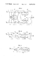
- FIG. 1 depicts a schematic block diagram of a prior art bandpass signal generator
- FIG. 2 illustrates a general block diagram of the signal generator in accordance with the principles of this invention
- FIG. 3 is a block diagram of the generator illustrated in FIG. 2 suitable for signals available in cartesian coordinates;
- FIG. 4 depicts the generator illustrated in FIG. 2 suitable for generating Phase Shift Keying modulated signals
- FIG. 5 is a block diagram of a particular embodiment of element 50 of FIG. 2 which is suitable for implementations which generate Differential Phase Shift Keying modulated signals.
- a bandpass signal generated by a data communication transmitter can be represented by ##EQU1## where a n and b n are the symbols to be transmitted, h(t) and g(t) are Nyguist pulses, T is a symbol period and ⁇ c is the carrier's radian frequency.
- equation (1) can be represented by ##EQU2##
- a perusal of equation (5) indicates that signal z(t) can be computed by sampling the C n signals, by convolving the sampled signals in a filter whose impulse response is e j .sup. ⁇ .sbsp.cnT R(t) e j .sup. ⁇ .sbsp.ct, and by summing the filter's output signals for all values of n.
- Equation (6) indicates that the bandpass signal s(t) may be implemented by combining the output signals of four circuits.
- a predetermined symbol signal (a n or b n ) is sampled and is applied to a filter having a predetermined impulse response (e.g., g(t)cos ⁇ c (nT+t)).
- a filter having a predetermined impulse response e.g., g(t)cos ⁇ c (nT+t).
- FIG. 1 is presented to illustrate an implementation of a prior art bandpass signal generator characterized by equation (6) and having ⁇ c /2 ⁇ related to T by a rational number.
- the symbol signals a n and b n are applied, in FIG. 1, to samplers 10 and 11, respectively, which may simply comprise controllable analog gates.
- the output signal of sampler 10 is applied to filters 20 and 21, and the output signal of sampler 11 is applied to filters 22 and 23.
- filters 20 and 21 are read-only-memory (ROM) units 30 and 31, respectively.
- Filter 20 in combination with ROM unit 30 is arranged to possess an impulse response g(t)cos ⁇ c (nT+t), which is variable with respect to n under control of ROM unit 30.
- Filter 21 in combination with ROM unit 31 is arranged to possess an impulse response h(t)cos ⁇ c (nT+t), which, as in the filter 20-ROM 30 interconnection, is variable with respect to n and is under control of ROM unit 31.
- Associated with filters 22 and 23 are ROM units 32 and 33, respectively. As in the filter 20-ROM 30 interconnection, each of filters 22 and 23 with its associated ROM unit possesses an impulse response which is variable with n and which is controlled as to this variability by the associated ROM unit.
- filter 22 is arranged to possess an impulse response characterized by h(t)sin ⁇ c (nT+t)
- filter 23 is arranged to possess an impulse response characterized by g(t)sin ⁇ c (nT+t).
- Element 40 of FIG. 1 develops the bandpass signal s(t) by arithmetically combining the output signals of filters 20, 21, 22 and 23. More specifically, signal s(t) is developed by summing the output signals of filters 20 and 22 with the negative of the output signals of filters 21 and 22.
- Element 40 may be an adder/subtractor circuit implemented in accordance with the teachings of I. Flores, The Logic of Computer Arithmetic, Prentice-Hall Inc., 1963, Chapter 4.
- the bandpass signal generator implementation of FIG. 1 requires extensive use of read-only-memories. Additionally, the FIG. 1 circuit requires the carrier frequency ⁇ c /2 ⁇ to be related to the symbol period T by a rational number.
- FIG. 2 is a block diagram of a circuit which in, accordance with the principles of this invention, is capable of developing the complex bandpass signal z(t) as defined by equation (7).
- the complex symbol signals C n are sampled in sampler 70 and are multiplied in complex multiplier 50 by the time precessing phasor e j .sup. ⁇ .sbsp.cnT which is increasing in phase with increasing n.
- multiplier 50 may be implemented with an adder which adds the phase angle of each C n signal to the phase angle ⁇ c nT.
- multiplier 50 may be implemented with a circuit for converting the applied cartesian coordinate C n signals to polar coordinate C n signals.
- multiplier 50 may comprise a plurality of multipliers for calculating the desired produce signals directly in cartesian coordinates.
- One embodiment of such a multiplier is described below in reference to FIG. 3.
- filter 60 possesses an impulse response characterized by R(t) e j .sup. ⁇ .sbsp.ct, where R(t) is as defined by equation (4).
- Filter 60 may, generally, be a recursive or a nonrecursive filter. Its specific embodiment, however, is dependent on the characteristics of the incoming signal (polar or cartesian) and on the user's preference.
- Equation (8) is similar in format to equation (6) in that both indicate the use of four filters. However, unlike the filters of equation (6), the impulse responses of the filters of equation (8) are not dependent on the variable n, and are therefore time invariant.
- FIG. 3 depicts a block diagram schematic for the cartesian coordinate implementation of the FIG. 2 circuit in accordance with equation (8).
- signals a n and b n are sampled at a rate of 1/T by sampling circuits 71 and 72, respectively.
- samplers 71 and 72 may comprise controllable analog gates.
- the sampled a n and b n symbol signals are applied, as in FIG. 2, to multiplier 50 wherein the sampled symbol signals are multiplied by the variable phasor e j .sup. ⁇ .sbsp.cnT.
- multiplier unit 51 multiplies the sampled a n signal by an applied cosine signal, cos ⁇ c nT
- multiplier unit 52 multiplies the sampled a n signal by an applied sine signal, sin ⁇ c nT.
- multiplier unit 53 multiplies the sampled b n signal by the applied sine signal, sin ⁇ c nT
- multiplier unit 54 multiplies the sampled b n signal by the applied cosine signal, cos ⁇ c nT.
- subtractor 55 the output signal of multiplier unit 53 is subtracted from the output signal of multiplier unit 51 to develop the signal (a n cos ⁇ c nT-b n sin ⁇ c nT) ⁇ (t-nT).
- adder 56 the output signal of multiplier unit 52 is added to the output signal of multiplier unit 54 to develop the signal (b n cos ⁇ c nT+a n sin ⁇ c nT) ⁇ (t-nT).
- the output signals of subtractor 55 and adder 56 are applied to filter block 60.
- the output signal from subtractor 55 is applied to filters 61 and 62 which respectively convolve their input signals with impulse responses g(t)cos ⁇ c t and h(t)sin ⁇ c t.
- the output signal from adder 56 is applied to filters 63 and 64 which respectively convolve their input signals with impulse responses h(t)cos ⁇ c t and g(t)sin ⁇ c t.
- the output signals of filters 62, 63 and 64 are subtracted from the output signal of filter 61 in summing network 65, providing thereby an output signal for filter 60 which is equal to the desired signal s(t) of equation (8).
- Summing network 65 may be implemented in a manner similar to the implementation of network 40 of FIG. 1.
- Filters 61-64 may be of any construction. They may be recursive filters or nonrecursive (transversal) filters. In some situations, however, transversal filters are preferable because of their linear phase characteristics and because of their ease of implementation.
- a transversal filter may simply comprise a shift register with signal taps at every stage of delay, means for multiplying the output signal of each tap by a filter coefficient, and means for adding the multiplied signals.
- Another advantage of non-recursive filters relates to the case of specifying a selected impulse response. As is well known, a transversal filter may be made to possess a selected impulse response simply by specifying the tap signal multiplication coefficients to be the sampled values of the desired impulse response.
- the sampled values of the desired impulse response are not obtained by sampling the impulse response at the symbol rate of sampling signals a n and b n (which is at the rate of 1/T seconds). Rather, the impulse response is sampled at a rate that relates to the digital realization of the bandpass signal s(t) in the digital transversal filters.
- the filter realization since the signal s(t) is centered about a carrier ⁇ c , the filter realization must proceed at a sampling rate that is at least equal to 2( ⁇ c +B) where B is half the bandwidth of s(t). That is the sampling rate which is used to obtain the transversal filters coefficients.
- the circuit of FIG. 3 implements the expression of equation (8), it can be appreciated that the FIG. 3 circuit is capable of generating signals having the form of equation (1).
- a number of specific modulation approaches have characteristic forms which may be classified as subsets of equation (1).
- PSK Phase Shift Keying
- a PSK signal can be written as ##EQU7## yielding a signal z(t) equal to ##EQU8## where e j .sup. ⁇ .sbsp.n defines the signal constellation C n (on the unit circle).
- the z(t) signal of equation (10) may be rewritten, yielding ##EQU9##
- the phasor multiplication of element 50 degenerates to a simple addition of the angles ⁇ n and ⁇ c nT.
- FIG. 4 is a block diagram of a PSK modulator characterized by equation (11). Contained in multiplication block 50 of FIG. 4 is an adder 57 and a read-only-memory (ROM) 58. Adder 57 sums the symbol signal ⁇ n (sampled by sampler 70) with the precessing angle ⁇ c nT, and ROM 58, in response to adder 57, develops the sine and cosine values of the summed angle ( ⁇ n + ⁇ c nT) on output leads 41 and 42, respectively.
- ROM read-only-memory
- adder 57 Since adder 57 sums angles, it must perform the summation in modulo 2 ⁇ . If ROM 58 contains the sine and cosine tables from 0 to 2 ⁇ in 2 k memory locations, then adder 57 has to operate in modulo 2 k . This, of course, is not a difficult requirement on adder 57 since all binary adders naturally do add in modulo 2 k , where k is the number of addition stages. Therefore, adder 57 may simply be a binary adder having k addition stages, and ROM 58 may be a memory having 2 k addresses -- storing in these addresses the values of the sine and cosine functions over the range of 0-2 ⁇ . To those skilled in the art, it will be apparent that in employing a small amount of logic circuitry, various trigonometric relationships of the sine and cosine function may be utilized to reduce the size of ROM 58.
- filter 66 convolves the cosine signal on lead 42 with an impulse response g(t)cos ⁇ c t
- filter 67 convolves the sine signal on lead 41 with an impulse response g(t) sin ⁇ c t.
- the output signal of filter 67 is subtracted from the output signal of filter 66 in unit 68, developing thereby an output signal of filter 60. It can be shown that the output signal of unit 68 is equal to the real part of the z(t) of equation (11), which is the desired s(t) signal.
- adder 57 may be simplified for special values of ⁇ c nT. In the extreme, if ⁇ c T is equal to 2 ⁇ , adder 57 may be completely eliminated since it adds in modulo 2 ⁇ and is, therefore, insensitive to input signals which equal to 2 ⁇ .
Abstract
Disclosed is apparatus for generating carrier signals modulated by baseband symbol signals. The disclosed apparatus includes samplers for sampling input symbol signals, multipliers for multiplying the sampled signals by a precessing phase that is a function of the carrier signal's frequency, and modified filters for convolving the multiplied signals with a complex (real and imaginary) low pass impulse response and for selecting the real part of the convolved signals.
Description
This invention relates to data communication apparatus and, more particularly, to apparatus for digitally generating bandpass signals.
Data transmission over voice frequency channels is generally accomplished by modulating a baseband data signal onto a carrier signal, developing thereby a bandpass signal, and then transmitting the modulated signal to a distant receiver wherein the signal is demodulated. The transmitter's modulation process generally includes low pass filtering to insure that the baseband signal is of a finite known bandwidth, modulating onto a carrier by means of any of a variety of modulation schemes, and bandpass filtering to insure that the transmitted signal occupies a finite known frequency band.
With the present trend of semiconductor technology toward large scale integration, a number of attempts have been made to implement the transmitter functions by digital techniques in a fashion that lends itself to integration. In an article entitled "In-Band Generation of Synchronous Linear Data Signals," IEEE Trans. on Comm., Vol. COM 21 No. 10, Oct. 1973, page 1116, Kalet and Weinstein describe a bandpass signal generator employing a finite number of fixed filters which, in combination, develop bandpass signals. In an article entitled, "Microcoded Modem Transmitters," IBM J. Res. Develop., July 1974, pp. 338-351, Choquet et al described a transmitter design employing a digital finite impulse response filter and programmable, cyclically modified, filter coefficients to obtain the desired bandpass signal. Both the Kalet and the Choquet apparatus are useful only when the ratio of the desired carrier frequency to the filters' processing rate is a rational number.
It is an object of this invention to provide a bandpass signal generator which is not limited to rational number ratios of carrier frequencies to a filter's processing rate.
This and other objects are achieved by multiplying a sampled applied input signal by a particularly defined precessing phasor signal and by convolving the product with a fixed low pass filter. More particularly, incoming symbol signals, which may comprise real and imaginary components, are sampled at a preselected rate. The sampled signals are multiplied by a time precessing phasor of unit magnitude, and the complex product signals are applied to a complex low pass filter. The low pass filter convolves the applied complex product signals with a particularly defined fixed impulse response and develops the real part of the convolved signals as the desired bandpass signal.
FIG. 1 depicts a schematic block diagram of a prior art bandpass signal generator;
FIG. 2 illustrates a general block diagram of the signal generator in accordance with the principles of this invention;
FIG. 3 is a block diagram of the generator illustrated in FIG. 2 suitable for signals available in cartesian coordinates;
FIG. 4 depicts the generator illustrated in FIG. 2 suitable for generating Phase Shift Keying modulated signals; and
FIG. 5 is a block diagram of a particular embodiment of element 50 of FIG. 2 which is suitable for implementations which generate Differential Phase Shift Keying modulated signals.
In general, a bandpass signal generated by a data communication transmitter can be represented by ##EQU1## where an and bn are the symbols to be transmitted, h(t) and g(t) are Nyguist pulses, T is a symbol period and ωc is the carrier's radian frequency. A Nyguist pulse g(t) is an analog signal having the property g(t-nT) = 0 for t = mT when m ≠ n, and g(0) = 1.
A more compact representation of equation (1) is obtained by using complex signals. Thus, equation (1) can be represented by ##EQU2## where
C.sub.n = a.sub.n + j b.sub.n (3)
and
R(t-nT) = g(t-nT) + j h(t-nT). (4)
in accordance with prior art teachings, the z(t) expression of equation (2) can be rewritten as ##EQU3## where δ(t-nT) is the standard delta function (δ(t)= 0 for all t≠0 and ∫δ(t)dt about 0 is 1), and where the symbol "*" designates convolution. A perusal of equation (5) indicates that signal z(t) can be computed by sampling the Cn signals, by convolving the sampled signals in a filter whose impulse response is ej.sup.ω.sbsp.cnT R(t) ej.sup.ω.sbsp.ct, and by summing the filter's output signals for all values of n. This is basically the approach taken by Kalet and Choquet as described in the aforementioned articles. From equation (2) it may be seen that the desired bandpass signal is obtained by evaluating the real part of z(t). Accordingly, substituting equations (3) and (4) into equation (5) and taking the real part thereof yields ##EQU4##
Equation (6) indicates that the bandpass signal s(t) may be implemented by combining the output signals of four circuits. In each one of the circuits, a predetermined symbol signal (an or bn) is sampled and is applied to a filter having a predetermined impulse response (e.g., g(t)cos ωc (nT+t)). It should be noted that all of the filters specified by equation (6) have an impulse response which is different for different values of n. Therefore, as n changes with time, so must the impulse response of the filters. It can be said, therefore, that implementation of the signal s(t) in accordance with the teachings of equation (6) requires the use of time varying filters.
If ωc /2π and T are not related by a rational number, the impulse responses required by equation (6) change in a noncyclical manner. Under such circumstances, the impulse response of the filters must be computed anew for each n=0,1,2, . . . ∞. Such computations require a substantial amount of hardware. If, on the other hand, ωc /2π and T are related by a rational number, then the necessary impulse responses repeat cyclically, permitting the use of impulse responses which are modified by the contents of a read-only-memory.
The cyclical repetition of the required impulse responses is the reason behind the "rational number" requirement of the Kalet and Choquet apparatus mentioned above.
In order to more fully appreciate the improvements comprising this invention, FIG. 1 is presented to illustrate an implementation of a prior art bandpass signal generator characterized by equation (6) and having ωc /2π related to T by a rational number. The symbol signals an and bn are applied, in FIG. 1, to samplers 10 and 11, respectively, which may simply comprise controllable analog gates. The output signal of sampler 10 is applied to filters 20 and 21, and the output signal of sampler 11 is applied to filters 22 and 23. Associated with filters 20 and 21 are read-only-memory (ROM) units 30 and 31, respectively. Filter 20 in combination with ROM unit 30 is arranged to possess an impulse response g(t)cos ωc (nT+t), which is variable with respect to n under control of ROM unit 30. Filter 21 in combination with ROM unit 31 is arranged to possess an impulse response h(t)cos ωc (nT+t), which, as in the filter 20-ROM 30 interconnection, is variable with respect to n and is under control of ROM unit 31. Associated with filters 22 and 23 are ROM units 32 and 33, respectively. As in the filter 20-ROM 30 interconnection, each of filters 22 and 23 with its associated ROM unit possesses an impulse response which is variable with n and which is controlled as to this variability by the associated ROM unit. In accordance with equation (6), filter 22 is arranged to possess an impulse response characterized by h(t)sin ωc (nT+t), and filter 23 is arranged to possess an impulse response characterized by g(t)sin ωc (nT+t).
As illustrated, the bandpass signal generator implementation of FIG. 1 requires extensive use of read-only-memories. Additionally, the FIG. 1 circuit requires the carrier frequency ωc /2π to be related to the symbol period T by a rational number.
These disadvantages have been eliminated in view of the discovery that the z(t) expression of equation (2) may be rewritten as ##EQU5## A perusal of equation (7) reveals that terms which vary with respect to n appear only on the left side of the convolution equation--which defines the applied signal--and not on the right side of the convolution equation--which defines the impulse response of the filter. Therefore, no time varying filters are necessary for developing the z(t) signal of equation (7). However, since the left hand side of equation (7) now has the ej.sup.ω.sbsp.cnT term, a time variation requirement is introduced on the sampled Cn signals (which are, of course, time varying).
On first blush, it appears that the time variation requirement by the ej.sup.ω.sbsp.cnT signal of equation (7) is identical to the filters' time variation requirement of equations (5) and (6) and that, therefore, no savings are realized. Upon a closer look, however, it can be seen that it is considerably easier to accurately multiply the Cn values by arbitrary phasors than it is to multiply whose sets of filter coefficients. First, there are fewer values to multiply (Cn signals generally take on only a small set of values), and second, for many applications, the relevant Cn signals lie on a unit circle. With such Cn signals (as will be shown below), multiplication by the phasor ej.sup.ω.sbsp.cnT takes the form of the simple addition of phase angles.
FIG. 2 is a block diagram of a circuit which in, accordance with the principles of this invention, is capable of developing the complex bandpass signal z(t) as defined by equation (7). In FIG. 2, the complex symbol signals Cn are sampled in sampler 70 and are multiplied in complex multiplier 50 by the time precessing phasor ej.sup.ω.sbsp.cnT which is increasing in phase with increasing n. If Cn is available in polar coordinates, multiplier 50 may be implemented with an adder which adds the phase angle of each Cn signal to the phase angle ωc nT. If Cn is available in cartesian coordinates, multiplier 50 may be implemented with a circuit for converting the applied cartesian coordinate Cn signals to polar coordinate Cn signals. Alternatively, multiplier 50 may comprise a plurality of multipliers for calculating the desired produce signals directly in cartesian coordinates. One embodiment of such a multiplier is described below in reference to FIG. 3.
The multiplied output signals of multiplier 50 of FIG. 2 are applied to filter 60. In accordance with equation (7), filter 60 possesses an impulse response characterized by R(t) ej.sup.ω.sbsp.ct, where R(t) is as defined by equation (4). Filter 60 may, generally, be a recursive or a nonrecursive filter. Its specific embodiment, however, is dependent on the characteristics of the incoming signal (polar or cartesian) and on the user's preference. When the Cn ej.sup.ω.sbsp.cnT signal is available in cartesian coordinates, it is generally found easier to perform the filtering process entirely in cartesian coordinates -- particularly since only the real part of the signal z(t) is desired as indicated by equation (2).
To characterize the hardware implementation of equation (7) in cartesian coordinates, it is necessary to substitute equations (3) and (4) into equation (7) and take the real part thereof, yielding ##EQU6##
Equation (8) is similar in format to equation (6) in that both indicate the use of four filters. However, unlike the filters of equation (6), the impulse responses of the filters of equation (8) are not dependent on the variable n, and are therefore time invariant.
FIG. 3 depicts a block diagram schematic for the cartesian coordinate implementation of the FIG. 2 circuit in accordance with equation (8).
In FIG. 3, signals an and bn are sampled at a rate of 1/T by sampling circuits 71 and 72, respectively. Like samplers 10 and 11 of FIG. 1, samplers 71 and 72 may comprise controllable analog gates. The sampled an and bn symbol signals are applied, as in FIG. 2, to multiplier 50 wherein the sampled symbol signals are multiplied by the variable phasor ej.sup.ω.sbsp.cnT. Within multiplier 50, multiplier unit 51 multiplies the sampled an signal by an applied cosine signal, cos ωc nT, and multiplier unit 52 multiplies the sampled an signal by an applied sine signal, sin ωc nT. Similarly with respect to the bn signal, multiplier unit 53 multiplies the sampled bn signal by the applied sine signal, sin ωc nT, and multiplier unit 54 multiplies the sampled bn signal by the applied cosine signal, cos ωc nT. In subtractor 55, the output signal of multiplier unit 53 is subtracted from the output signal of multiplier unit 51 to develop the signal (an cos ωc nT-bn sin ωc nT)δ(t-nT). In adder 56, the output signal of multiplier unit 52 is added to the output signal of multiplier unit 54 to develop the signal (bn cos ωc nT+an sin ωc nT)δ(t-nT). The output signals of subtractor 55 and adder 56 are applied to filter block 60.
Within filter 60, the output signal from subtractor 55 is applied to filters 61 and 62 which respectively convolve their input signals with impulse responses g(t)cos ωc t and h(t)sin ωc t. Similarly, the output signal from adder 56 is applied to filters 63 and 64 which respectively convolve their input signals with impulse responses h(t)cos ωc t and g(t)sin ωc t. Also within filter 60, the output signals of filters 62, 63 and 64 are subtracted from the output signal of filter 61 in summing network 65, providing thereby an output signal for filter 60 which is equal to the desired signal s(t) of equation (8). Summing network 65 may be implemented in a manner similar to the implementation of network 40 of FIG. 1.
Filters 61-64 may be of any construction. They may be recursive filters or nonrecursive (transversal) filters. In some situations, however, transversal filters are preferable because of their linear phase characteristics and because of their ease of implementation. For example, a transversal filter may simply comprise a shift register with signal taps at every stage of delay, means for multiplying the output signal of each tap by a filter coefficient, and means for adding the multiplied signals. Another advantage of non-recursive filters relates to the case of specifying a selected impulse response. As is well known, a transversal filter may be made to possess a selected impulse response simply by specifying the tap signal multiplication coefficients to be the sampled values of the desired impulse response.
Of course, the sampled values of the desired impulse response are not obtained by sampling the impulse response at the symbol rate of sampling signals an and bn (which is at the rate of 1/T seconds). Rather, the impulse response is sampled at a rate that relates to the digital realization of the bandpass signal s(t) in the digital transversal filters. In accordance with well-known sampling theorems, since the signal s(t) is centered about a carrier ωc, the filter realization must proceed at a sampling rate that is at least equal to 2(ωc +B) where B is half the bandwidth of s(t). That is the sampling rate which is used to obtain the transversal filters coefficients.
Since the circuit of FIG. 3 implements the expression of equation (8), it can be appreciated that the FIG. 3 circuit is capable of generating signals having the form of equation (1). A number of specific modulation approaches, however, have characteristic forms which may be classified as subsets of equation (1). For example, the familiar expressions for Quadrature Amplitude Modulation (QAM) and Differential Phase Shift Keying modulation (DPSK) can be obtained by letting h(t)=0 in equation (1). Similarly, the expression for Single Sideband modulation may be obtained by lettering bn = 0. From the above, it may be realized that for specific modulation approaches, the implementation of the FIG. 2 circuit is simpler than shown in FIG. 3. The following are some of the more unusual examples.
A PSK signal can be written as ##EQU7## yielding a signal z(t) equal to ##EQU8## where ej.sup.φ.sbsp.n defines the signal constellation Cn (on the unit circle). In accordance with equation (7), the z(t) signal of equation (10) may be rewritten, yielding ##EQU9## Interestingly, the phasor multiplication of element 50 degenerates to a simple addition of the angles φn and ωc nT.
FIG. 4 is a block diagram of a PSK modulator characterized by equation (11). Contained in multiplication block 50 of FIG. 4 is an adder 57 and a read-only-memory (ROM) 58. Adder 57 sums the symbol signal φn (sampled by sampler 70) with the precessing angle ωc nT, and ROM 58, in response to adder 57, develops the sine and cosine values of the summed angle (φn + ωc nT) on output leads 41 and 42, respectively.
Since adder 57 sums angles, it must perform the summation in modulo 2π. If ROM 58 contains the sine and cosine tables from 0 to 2π in 2k memory locations, then adder 57 has to operate in modulo 2k. This, of course, is not a difficult requirement on adder 57 since all binary adders naturally do add in modulo 2k, where k is the number of addition stages. Therefore, adder 57 may simply be a binary adder having k addition stages, and ROM 58 may be a memory having 2k addresses -- storing in these addresses the values of the sine and cosine functions over the range of 0-2π. To those skilled in the art, it will be apparent that in employing a small amount of logic circuitry, various trigonometric relationships of the sine and cosine function may be utilized to reduce the size of ROM 58.
Within filter block 60 of FIG. 4, filter 66 convolves the cosine signal on lead 42 with an impulse response g(t)cos ωc t, and filter 67 convolves the sine signal on lead 41 with an impulse response g(t) sin ωc t. The output signal of filter 67 is subtracted from the output signal of filter 66 in unit 68, developing thereby an output signal of filter 60. It can be shown that the output signal of unit 68 is equal to the real part of the z(t) of equation (11), which is the desired s(t) signal.
In DPSK Modulation, the transmitted signal has the form of equation (9) but the transmitted symbol is contained in a differential angle Δφn = φn - φn -1. To obtain the (φn + ωc nT) signal required at the input terminal of ROM 58 of FIG. 4, it is only necessary to replace the precessing ωc nT signal applied to adder 57 with a fixed ωc T signal, and to interpose an accumulator 59, as depicted in FIG. 5, between adder 57 and ROM 58. By applying the symbol signal Δφn to adder 57 together with the fixed ωc T signal, the accumulated output signal developed by accumulator 59 is ##EQU10## which is equal to φn + ωc nT as required by equation (9).
Interestingly, adder 57 may be simplified for special values of ωc nT. In the extreme, if ωc T is equal to 2π, adder 57 may be completely eliminated since it adds in modulo 2π and is, therefore, insensitive to input signals which equal to 2π.
Claims (22)
1. A bandpass signal generator comprising:
means for sampling applied input signals at a preselected rate;
means for multiplying the output signals of said means for sampling by a phasor whose angle is advanced by a preselected additive constant at each sampling interval of said means for sampling; and
means for convolving the output signal of said means for multiplying with a preselected impulse response.
2. Apparatus responsive to symbol signals applied at a predetermined rate 1/T, for generating a carrier signal of preselected frequency ωc modulated by said symbol signals comprising:
means for sampling said symbol signals at said predetermined rate;
means for multiplying the sampled signals by a phasor ej.sup.ω.sbsp.cnT where n is an integer which is continually increasing with each sampled symbol signal; and
means for convolving the output signal of said means for multiplying with a complex predetermined impulse response.
3. The apparatus of claim 2, wherein said means for convolving develops a real signal.
4. The apparatus of claim 2 wherein said means for convolving generates a convolution product of said output signal of said means for multiplying with a fixed impulse response and develops an output signal representative of the real part of said convolution product.
5. The apparatus of claim 4 wherein said fixed impulse response is of a class providing low pass filtering.
6. The apparatus of claim 4 wherein said impulse response is [g(t) + j h (t)]ej.sup.ω.sbsp.ct where g(t) and h(t) are Nyguist pulses.
7. The apparatus of claim 2 wherein said symbol signals contain real components an and imaginary components bn.
8. Apparatus for generating a modulated carrier signal s(t) of the form ##EQU11## where ωc is the radian carrier frequency of said carrier signal, an and bn are symbol signals, g(t) and h(t) are Nyguist pulses, T is the symbol period, and n is a variable integer incremented with each symbol period, comprising:
first means for sampling said an and bn symbol signals at a periodicity of T to develop sampled signals an δ(t-nT) and bn δ(t-nT), respectively;
second means for combining nonzero ones of said sampled symbol signals with a cos ωc nT signal and with a sin ωc nt signal to develop a first signal and a second signal;
third means for convolving said first and second signals by a plurality of preselected impulse responses to develop a like plurality of filtered signals; and
fourth means for arithmetically combining said plurality of filtered signals.
9. The apparatus of claim 8 wherein said second means comprises:
means for multiplying each nonzero one of said sampled symbol signals by a cos ωc nT signal and a sin ωc nT signal, developing thereby product signals;
means for arithmetically joining selected ones of said product signals to develop a said first signal representative of the signal (an cos ωc nT - bn sin ωc nT)δ(t-nT) and said second signal representative of the signal (an sin ωc nT + bn cos ωc nT)δ(t-nT).
10. The apparatus of claim 9 wherein said third means comprises:
first and second filters for convolving said first signal by g(t)cos ωc t and h(t)sin ωc t, respectively; and
third and fourth filters for convolving said second signal by g(t)sin ωc t and h(t)cos ωc t, respectively.
11. The apparatus of claim 10 wherein said means for arithmetically joining comprises:
means for subtracting the output signals of said second, third and fourth filters from the output signal of said first filter.
12. The apparatus of claim 9 wherein said h(t) Nyguist pulse is equal to zero and wherein said third means comprises a first filter for convolving said first signal by g(t)cos ωc t and a second filter for convolving said second signal by g(t)sin ωc t.
13. The apparatus of claim 9 wherein said g(t) Nyguist pulse is equal to zero and wherein said third means comprises a first filter for convolving said first signal by h(t)sin ωc t and a second filter for convolving said second signal by h(t)cos ωc t.
14. The apparatus of claim 9 wherein either one of said symbol signals is equal to zero, leaving one nonzero sampled symbol signal, and wherein said second means comprises:
fifth means for multiplying said nonzero sampled symbol signal by said cos ωc nT signal; and
sixth means for multiplying said nonzero sampled signal by said sin ωc nT signal.
15. The apparatus of claim 14 wherein said third means comprises:
first and second filters for convolving said first signal by g(t)cos ωc t and h(t)sin ωc t, respectively, and
third and fourth filters for convolving said second signal by g(t)sin ωc t and h(t)cos ωc t, respectively.
16. The apparatus of claim 14 wherein said means for arithmetically joining comprises:
means for subtracting the output signals of said second, third, and fourth filters from the output signal of said first filter.
17. The apparatus of claim 14 wherein said h(t) Nyguist pulse is equal to zero and wherein said means for convolving comprises a first filter for convolving said first signal by g(t)cos ωc t and a second filter for convolving said second signal by g(t)sin ωc t.
18. The apparatus of claim 14 wherein said g(t) Nyguist pulse is equal to zero and wherein said means for convolving comprises a first filter for convolving said first signal by h(t)sin ωc t and a second filter for convolving said second signal by h(t)cos ωc t.
19. Apparatus for developing modulated signals of the form ##EQU12## where ωc is a radian carrier frequency, φn is a phase angle signal related to an applied symbol signal, g(t) is a Nyguist pulse, T is the symbol period, and n is an integer variable continually incrementing with each symbol period, comprising:
means for developing a cosine signal and a sine signal of an angle representative of the sum of said φn signal and of a precessing angle ωc nT;
means for convolving said developed cosine and sine signals with preselected fixed impulse responses; and
means for arithmetically combining the output signals of said means for convolving.
20. The apparatus of claim 19 wherein said means for developing comprises:
means for sampling said φn signal;
addition means for adding said sampled φn signal with said precessing phase angle ωc nT; and
means responsive to said addition means for developing said sine and cosine signals.
21. The apparatus of claim 19 wherein said means for convolving comprises:
a first filter for convolving said cosine signal with g(t)cos ωc t; and
a second filter for convolving said sine signal with g(t)sin ωc t.
22. The apparatus of claim 19 wherein said means for developing comprises;
means for sampling applied symbol signals Δφn, where Δφn is related to said phase angle signal φn by the relation φn = φn -1 + Δφn ;
addition means for adding said sampled Δφn signals to a fixed phase angle ωc T;
means for accumulating the output signals of said addition means; and
means responsive to said means for accumulating for developing said sine and cosine signals.
Priority Applications (1)
| Application Number | Priority Date | Filing Date | Title |
|---|---|---|---|
| US05/636,563 US4015222A (en) | 1975-12-01 | 1975-12-01 | Modulated passband signal generator |
Applications Claiming Priority (1)
| Application Number | Priority Date | Filing Date | Title |
|---|---|---|---|
| US05/636,563 US4015222A (en) | 1975-12-01 | 1975-12-01 | Modulated passband signal generator |
Publications (1)
| Publication Number | Publication Date |
|---|---|
| US4015222A true US4015222A (en) | 1977-03-29 |
Family
ID=24552435
Family Applications (1)
| Application Number | Title | Priority Date | Filing Date |
|---|---|---|---|
| US05/636,563 Expired - Lifetime US4015222A (en) | 1975-12-01 | 1975-12-01 | Modulated passband signal generator |
Country Status (1)
| Country | Link |
|---|---|
| US (1) | US4015222A (en) |
Cited By (15)
| Publication number | Priority date | Publication date | Assignee | Title |
|---|---|---|---|---|
| FR2498398A1 (en) * | 1981-01-22 | 1982-07-23 | Codex Corp | DATA MODULATOR FOR A MODEM |
| EP0083629A1 (en) * | 1981-07-13 | 1983-07-20 | Western Electric Company, Incorporated | Data signal echo canceller |
| US4433310A (en) * | 1979-12-31 | 1984-02-21 | Bic Jean Claude | Modulator-demodulator for four level double amplitude modulation on quadrature carriers |
| US4638504A (en) * | 1985-06-28 | 1987-01-20 | Broadcast Electronics, Inc. | Independent channel modulation system for AM stereo |
| JPH0211057A (en) * | 1988-03-22 | 1990-01-16 | American Teleph & Telegr Co <Att> | Data communication method and communication network |
| US5036296A (en) * | 1989-09-13 | 1991-07-30 | Nec Corporation | Frequency tracking circuit using samples equalized at different sampling instants of same clock period |
| EP0485105A2 (en) | 1990-11-07 | 1992-05-13 | AT&T Corp. | Coding for digital transmission |
| US5438301A (en) * | 1994-07-25 | 1995-08-01 | At&T Corp. | Modem having a phase corrector and a voltage controlled oscillator implemented using a multi-stage ring oscillator |
| DE4409362A1 (en) * | 1994-03-18 | 1995-09-21 | Siemens Ag | Circuit forming linguistic intermediate value |
| US5825829A (en) * | 1995-06-30 | 1998-10-20 | Scientific-Atlanta, Inc. | Modulator for a broadband communications system |
| US6031874A (en) * | 1997-09-26 | 2000-02-29 | Ericsson Inc. | Unequal error protection in coded modulation schemes |
| US6356594B1 (en) * | 1998-11-03 | 2002-03-12 | Motorola, Inc. | Data converter |
| US6504879B1 (en) * | 1998-07-17 | 2003-01-07 | Fujitsu Limited | Digital modulation apparatus |
| WO2005114941A1 (en) * | 2004-05-20 | 2005-12-01 | Anatoliy Arkadievich Kokhan | Method for accurate prototype modulation |
| WO2008108681A1 (en) * | 2007-03-02 | 2008-09-12 | Andrei Vitalyevich Pargachev | Method for forming modulated radio signal without side spectra and harmonics |
Citations (1)
| Publication number | Priority date | Publication date | Assignee | Title |
|---|---|---|---|---|
| US3671670A (en) * | 1970-04-15 | 1972-06-20 | Bell Telephone Labor Inc | Digital filter frequency-shift modulator |
-
1975
- 1975-12-01 US US05/636,563 patent/US4015222A/en not_active Expired - Lifetime
Patent Citations (1)
| Publication number | Priority date | Publication date | Assignee | Title |
|---|---|---|---|---|
| US3671670A (en) * | 1970-04-15 | 1972-06-20 | Bell Telephone Labor Inc | Digital filter frequency-shift modulator |
Non-Patent Citations (3)
| Title |
|---|
| Choquet et al., "Microcoded Modem Transmitters," IBM Journal of Research and Development, July, 1974, pp. 338-351. |
| Choquet et al., "Microcoded Modem Transmitters," IBM Journal of Research and Development, July, 1974, pp. 338-351. * |
| Kalet et al., "In-Band Generation of Synchronous Linear Data Signals" IEEE Transactions on Communications, vol. COM-21, Oct. 1973, pp. 1116-1122. * |
Cited By (18)
| Publication number | Priority date | Publication date | Assignee | Title |
|---|---|---|---|---|
| US4433310A (en) * | 1979-12-31 | 1984-02-21 | Bic Jean Claude | Modulator-demodulator for four level double amplitude modulation on quadrature carriers |
| FR2498398A1 (en) * | 1981-01-22 | 1982-07-23 | Codex Corp | DATA MODULATOR FOR A MODEM |
| EP0083629A1 (en) * | 1981-07-13 | 1983-07-20 | Western Electric Company, Incorporated | Data signal echo canceller |
| EP0083629A4 (en) * | 1981-07-13 | 1983-10-26 | Western Electric Co | Data signal echo canceller. |
| US4464545A (en) * | 1981-07-13 | 1984-08-07 | Bell Telephone Laboratories, Incorporated | Echo canceller |
| US4638504A (en) * | 1985-06-28 | 1987-01-20 | Broadcast Electronics, Inc. | Independent channel modulation system for AM stereo |
| JP2547844B2 (en) | 1988-03-22 | 1996-10-23 | アメリカン テレフォン アンド テレグラフ カムパニー | Data communication method and communication network |
| JPH0211057A (en) * | 1988-03-22 | 1990-01-16 | American Teleph & Telegr Co <Att> | Data communication method and communication network |
| US5036296A (en) * | 1989-09-13 | 1991-07-30 | Nec Corporation | Frequency tracking circuit using samples equalized at different sampling instants of same clock period |
| EP0485105A2 (en) | 1990-11-07 | 1992-05-13 | AT&T Corp. | Coding for digital transmission |
| DE4409362A1 (en) * | 1994-03-18 | 1995-09-21 | Siemens Ag | Circuit forming linguistic intermediate value |
| US5438301A (en) * | 1994-07-25 | 1995-08-01 | At&T Corp. | Modem having a phase corrector and a voltage controlled oscillator implemented using a multi-stage ring oscillator |
| US5825829A (en) * | 1995-06-30 | 1998-10-20 | Scientific-Atlanta, Inc. | Modulator for a broadband communications system |
| US6031874A (en) * | 1997-09-26 | 2000-02-29 | Ericsson Inc. | Unequal error protection in coded modulation schemes |
| US6504879B1 (en) * | 1998-07-17 | 2003-01-07 | Fujitsu Limited | Digital modulation apparatus |
| US6356594B1 (en) * | 1998-11-03 | 2002-03-12 | Motorola, Inc. | Data converter |
| WO2005114941A1 (en) * | 2004-05-20 | 2005-12-01 | Anatoliy Arkadievich Kokhan | Method for accurate prototype modulation |
| WO2008108681A1 (en) * | 2007-03-02 | 2008-09-12 | Andrei Vitalyevich Pargachev | Method for forming modulated radio signal without side spectra and harmonics |
Similar Documents
| Publication | Publication Date | Title |
|---|---|---|
| US4015222A (en) | Modulated passband signal generator | |
| US4130806A (en) | Filter and demodulation arrangement | |
| US4152649A (en) | Channel equalization apparatus and method using the Fourier transform technique | |
| US4974236A (en) | Arrangement for generating an SSB signal | |
| CA1177893A (en) | Digital modem transmitter | |
| US3524169A (en) | Impulse response correction system | |
| US5048058A (en) | MSK modulation and differentially coherent detection transmission system | |
| US4468794A (en) | Digital coherent detector | |
| AU573966B2 (en) | Zero-if digital receiver | |
| US4812786A (en) | Method and system for providing precise multi-function modulation | |
| US5828707A (en) | Differential detecting apparatus for detecting phase difference of phase-modulated signal | |
| US5057786A (en) | Quadrature amplitude modulation wave demodulator provided with band-pass filters for fixed equalizer | |
| US3430143A (en) | Communications system wherein information is represented by the phase difference between adjacent tones | |
| US4416016A (en) | Differential phase shift keyed receiver | |
| US3387220A (en) | Apparatus and method for synchronously demodulating frequency modulated differentially coherent duobinary signals | |
| US3803501A (en) | Frequency discriminator using digital non-recursive filters | |
| US4794556A (en) | Method and apparatus for sampling in-phase and quadrature components | |
| EP0695028B1 (en) | Small-scale signal adding device and differential detecting device | |
| US4010360A (en) | Carrier-compatible chirp-z transform device | |
| EP0155049B1 (en) | Transmission system for the transmission of data signals in a modulation band | |
| JPH05110369A (en) | Phase shifter | |
| GB1594320A (en) | Method and device for measuring the difference in envelope delay at the extreme frequences of channel passband in a data transmission system | |
| JP2003188747A (en) | Distortion compensation transmitter | |
| AU650170B2 (en) | Phase divider for complex signals | |
| US6184756B1 (en) | Modulator |