US4126383A - Electrooptic display device - Google Patents
Electrooptic display device Download PDFInfo
- Publication number
- US4126383A US4126383A US05/792,591 US79259177A US4126383A US 4126383 A US4126383 A US 4126383A US 79259177 A US79259177 A US 79259177A US 4126383 A US4126383 A US 4126383A
- Authority
- US
- United States
- Prior art keywords
- display device
- circuit board
- recited
- electrooptical display
- light
- Prior art date
- Legal status (The legal status is an assumption and is not a legal conclusion. Google has not performed a legal analysis and makes no representation as to the accuracy of the status listed.)
- Expired - Lifetime
Links
- 239000004973 liquid crystal related substance Substances 0.000 claims abstract description 16
- 239000000463 material Substances 0.000 claims description 11
- 210000002858 crystal cell Anatomy 0.000 claims description 9
- 229920001225 polyester resin Polymers 0.000 claims description 9
- 239000004645 polyester resin Substances 0.000 claims description 9
- 239000000758 substrate Substances 0.000 claims description 9
- 210000004027 cell Anatomy 0.000 claims description 8
- 229920003023 plastic Polymers 0.000 claims description 8
- 239000004033 plastic Substances 0.000 claims description 7
- 239000004744 fabric Substances 0.000 claims description 5
- 239000011152 fibreglass Substances 0.000 claims description 5
- GWEVSGVZZGPLCZ-UHFFFAOYSA-N Titan oxide Chemical compound O=[Ti]=O GWEVSGVZZGPLCZ-UHFFFAOYSA-N 0.000 claims description 4
- 229910052782 aluminium Inorganic materials 0.000 claims description 4
- XAGFODPZIPBFFR-UHFFFAOYSA-N aluminium Chemical compound [Al] XAGFODPZIPBFFR-UHFFFAOYSA-N 0.000 claims description 4
- TZCXTZWJZNENPQ-UHFFFAOYSA-L barium sulfate Chemical compound [Ba+2].[O-]S([O-])(=O)=O TZCXTZWJZNENPQ-UHFFFAOYSA-L 0.000 claims description 4
- VYZAMTAEIAYCRO-UHFFFAOYSA-N Chromium Chemical compound [Cr] VYZAMTAEIAYCRO-UHFFFAOYSA-N 0.000 claims description 3
- BQCADISMDOOEFD-UHFFFAOYSA-N Silver Chemical compound [Ag] BQCADISMDOOEFD-UHFFFAOYSA-N 0.000 claims description 3
- 229910052804 chromium Inorganic materials 0.000 claims description 3
- 239000011651 chromium Substances 0.000 claims description 3
- PCHJSUWPFVWCPO-UHFFFAOYSA-N gold Chemical compound [Au] PCHJSUWPFVWCPO-UHFFFAOYSA-N 0.000 claims description 3
- 229910052737 gold Inorganic materials 0.000 claims description 3
- 239000010931 gold Substances 0.000 claims description 3
- 239000002985 plastic film Substances 0.000 claims description 3
- 229920006255 plastic film Polymers 0.000 claims description 3
- 229910052709 silver Inorganic materials 0.000 claims description 3
- 239000004332 silver Substances 0.000 claims description 3
- 229910018404 Al2 O3 Inorganic materials 0.000 claims description 2
- 239000011248 coating agent Substances 0.000 claims description 2
- 238000000576 coating method Methods 0.000 claims description 2
- CPLXHLVBOLITMK-UHFFFAOYSA-N magnesium oxide Inorganic materials [Mg]=O CPLXHLVBOLITMK-UHFFFAOYSA-N 0.000 claims description 2
- 238000007788 roughening Methods 0.000 claims description 2
- 238000000149 argon plasma sintering Methods 0.000 claims 6
- 238000004026 adhesive bonding Methods 0.000 claims 1
- 239000012254 powdered material Substances 0.000 claims 1
- 230000005540 biological transmission Effects 0.000 abstract description 5
- 238000005286 illumination Methods 0.000 description 9
- 230000008020 evaporation Effects 0.000 description 4
- 238000001704 evaporation Methods 0.000 description 4
- 238000000034 method Methods 0.000 description 3
- 229920000728 polyester Polymers 0.000 description 3
- 210000000707 wrist Anatomy 0.000 description 3
- 230000008901 benefit Effects 0.000 description 2
- 238000004519 manufacturing process Methods 0.000 description 2
- 239000003973 paint Substances 0.000 description 2
- 229920002799 BoPET Polymers 0.000 description 1
- 239000005041 Mylar™ Substances 0.000 description 1
- 239000004677 Nylon Substances 0.000 description 1
- 230000009471 action Effects 0.000 description 1
- 230000008859 change Effects 0.000 description 1
- 230000003098 cholesteric effect Effects 0.000 description 1
- 239000004020 conductor Substances 0.000 description 1
- 239000002178 crystalline material Substances 0.000 description 1
- 230000000694 effects Effects 0.000 description 1
- 238000005516 engineering process Methods 0.000 description 1
- 239000003822 epoxy resin Substances 0.000 description 1
- 239000010408 film Substances 0.000 description 1
- 239000010419 fine particle Substances 0.000 description 1
- 239000011888 foil Substances 0.000 description 1
- 239000003292 glue Substances 0.000 description 1
- 239000007788 liquid Substances 0.000 description 1
- 229910052751 metal Inorganic materials 0.000 description 1
- 239000002184 metal Substances 0.000 description 1
- 150000002739 metals Chemical class 0.000 description 1
- 230000004048 modification Effects 0.000 description 1
- 238000012986 modification Methods 0.000 description 1
- 229920001778 nylon Polymers 0.000 description 1
- 229920000647 polyepoxide Polymers 0.000 description 1
- 230000008569 process Effects 0.000 description 1
- 238000005488 sandblasting Methods 0.000 description 1
- 238000007650 screen-printing Methods 0.000 description 1
- 239000000126 substance Substances 0.000 description 1
- 239000010409 thin film Substances 0.000 description 1
Images

Classifications
-
- G—PHYSICS
- G02—OPTICS
- G02F—OPTICAL DEVICES OR ARRANGEMENTS FOR THE CONTROL OF LIGHT BY MODIFICATION OF THE OPTICAL PROPERTIES OF THE MEDIA OF THE ELEMENTS INVOLVED THEREIN; NON-LINEAR OPTICS; FREQUENCY-CHANGING OF LIGHT; OPTICAL LOGIC ELEMENTS; OPTICAL ANALOGUE/DIGITAL CONVERTERS
- G02F1/00—Devices or arrangements for the control of the intensity, colour, phase, polarisation or direction of light arriving from an independent light source, e.g. switching, gating or modulating; Non-linear optics
- G02F1/01—Devices or arrangements for the control of the intensity, colour, phase, polarisation or direction of light arriving from an independent light source, e.g. switching, gating or modulating; Non-linear optics for the control of the intensity, phase, polarisation or colour
- G02F1/13—Devices or arrangements for the control of the intensity, colour, phase, polarisation or direction of light arriving from an independent light source, e.g. switching, gating or modulating; Non-linear optics for the control of the intensity, phase, polarisation or colour based on liquid crystals, e.g. single liquid crystal display cells
- G02F1/133—Constructional arrangements; Operation of liquid crystal cells; Circuit arrangements
- G02F1/1333—Constructional arrangements; Manufacturing methods
- G02F1/1335—Structural association of cells with optical devices, e.g. polarisers or reflectors
- G02F1/1336—Illuminating devices
- G02F1/133615—Edge-illuminating devices, i.e. illuminating from the side
-
- G—PHYSICS
- G02—OPTICS
- G02F—OPTICAL DEVICES OR ARRANGEMENTS FOR THE CONTROL OF LIGHT BY MODIFICATION OF THE OPTICAL PROPERTIES OF THE MEDIA OF THE ELEMENTS INVOLVED THEREIN; NON-LINEAR OPTICS; FREQUENCY-CHANGING OF LIGHT; OPTICAL LOGIC ELEMENTS; OPTICAL ANALOGUE/DIGITAL CONVERTERS
- G02F1/00—Devices or arrangements for the control of the intensity, colour, phase, polarisation or direction of light arriving from an independent light source, e.g. switching, gating or modulating; Non-linear optics
- G02F1/01—Devices or arrangements for the control of the intensity, colour, phase, polarisation or direction of light arriving from an independent light source, e.g. switching, gating or modulating; Non-linear optics for the control of the intensity, phase, polarisation or colour
- G02F1/13—Devices or arrangements for the control of the intensity, colour, phase, polarisation or direction of light arriving from an independent light source, e.g. switching, gating or modulating; Non-linear optics for the control of the intensity, phase, polarisation or colour based on liquid crystals, e.g. single liquid crystal display cells
- G02F1/133—Constructional arrangements; Operation of liquid crystal cells; Circuit arrangements
- G02F1/1333—Constructional arrangements; Manufacturing methods
- G02F1/1335—Structural association of cells with optical devices, e.g. polarisers or reflectors
-
- G—PHYSICS
- G04—HOROLOGY
- G04G—ELECTRONIC TIME-PIECES
- G04G9/00—Visual time or date indication means
- G04G9/0023—Visual time or date indication means by light valves in general
- G04G9/0029—Details
- G04G9/0035—Details constructional
- G04G9/0041—Illumination devices
-
- G—PHYSICS
- G09—EDUCATION; CRYPTOGRAPHY; DISPLAY; ADVERTISING; SEALS
- G09F—DISPLAYING; ADVERTISING; SIGNS; LABELS OR NAME-PLATES; SEALS
- G09F9/00—Indicating arrangements for variable information in which the information is built-up on a support by selection or combination of individual elements
- G09F9/30—Indicating arrangements for variable information in which the information is built-up on a support by selection or combination of individual elements in which the desired character or characters are formed by combining individual elements
Definitions
- the present invention relates to an electrooptic display device and a process for its manufacture.
- Electrooptical display devices have found application in various electronic instruments.
- the readability of passive liquid crystal displays, which emit no light of their own, is mainly determined by the brightness and the direction of the surrounding illumination. Additional illumination can be provided by building light sources into the display itself by this requires additional space which is generally not available in compact instruments such as electronic clocks, wrist watches and pocket calculators.
- one object of this invention is to create an electrooptic display device which requires little energy to operate, which occupies only a small space, and which can be read even when the surrounding illumination is very low.
- the present invention comprises a display, which can be operated either in the transmission or reflection modes consisting of a liquid crystal display cell and a semitransparent reflector located in or on a circuit board. It is possible to build a very compact display device with built-in illumination by employing a circuit board which is at least partially light conducting. At least part of the circuit board of this invention is manufactured by combining a reflecting layer, which is produced by the partial evaporation of a reflective material on a substrate or the evaporation of a reflective material on one side of a mesh, with a light diffusing substance, and embedding these two materials together in a transparent polyester or epoxy resin. Metals such as aluminum, silver, gold, chromium, etc. are especially good materials to evaporate onto a substrate to produce a reflective layer.
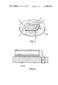
- FIG. 1 shows a cross section of a prior art display device.
- FIG. 2 shows a perspective view of a display device designed for a wrist watch.
- FIG. 3 shows a cross sectional view of the display device in FIG. 2.
- FIG. 4 shows the various layers comprising the circuit board in a preferred embodiment of the invention.
- the prior art display device shown in FIG. 1 contains a commercially available liquid crystal cell 1, schematically illustrated by a front cell plate 1.1, a rear cell plate 1.2 on the reflector side of the device, and a layer of liquid crystalline material 1.3 located between the two cell plates 1.1 and 1.2.
- a transparent plastic element 2 is located underneath the liquid crystal cell 1, and its upper surface 2.1 is roughened to make it light diffusing. The remainder of the upper part of this plastic element is coated with white paint 2.2. Part of the plastic element is hollowed out 2.3 to receive a miniature lamp 3.
- the light that is emitted by the miniature lamp 3 is reflected by the white coating 2.2 and a reflector foil 4 located under the plastic element and emerges through the light diffusing surface 2.1 of the plastic element 2 to act as rear illumination for the liquid crystal cell 1.
- a disadvantage of this type of display device is the use of the rather thick light conducting plastic element 2 which requires a considerable increase in the amount of space required for the display.
- the basic idea of this invention is to minimize the space required for the display device by incorporating all of the elements required to illuminate the liquid crystal cell 1 into a single element which already exists within the instrument.
- FIG. 2 shows a liquid crystal display designed for a wrist watch whose illumination system is built directly into the circuit board 20 of the watch module.
- the conductors 12 connect the segment electrodes 10 of the liquid crystal cell 1 with the pins 11 of an integrated circuit 30 (not shown).
- a miniature lamp 3 is built into the circuit board 30 near its periphery where there is a light conducting region.
- FIG. 3 gives a simplified cross sectional view of the essential parts of this invention that are illustrated in FIG. 2.
- a semitransparent reflector 1.4 is, as is suggested in the German Patent Disclosure No. 2,531,372.8, attached directly to a polarizer which is cemented to the rear cell plate 1.2.
- the display device depicted in FIGS. 2 and 3 functions as follows: as long as there is sufficient surrounding illumination the liquid crystal display is read in the reflection mode where the semitransparent reflector 1.4 reflects the incident light back through the cell to the observer. However, if the illumination is not bright enough, then the display can be read in the transmission mode by intermittently turning on the miniature lamp 3 so that its light will be conducted through at least part of the circuit board 20 and emerge through the region behind the semitransparent reflector 1.4 to illuminate the display from behind.
- the preferred embodiment of the circuit board 20 consists of six layers of light conducting polyester resin 21 with four sheets of fiberglass cloth 22 glued in between the first five polyester layers.
- a substrate 24, which has reflecting regions 23, is embedded between the last two polyester layers.
- the substrate 24 is a piece of 100 ⁇ m thick Mylar film, and the reflecting regions 23 consist of aluminum which is evaporated onto a substrate 24 through the square openings of a monofilament screen which is placed in direct contact with the substrate.
- An array of square reflecting regions 23 100 ⁇ m on a side, 0.5 ⁇ m thick and with 50 ⁇ m spacing is produced by this technique.
- the use of this type of reflector has the advantage that it does not short circuit the components placed on the circuit board since the reflecting regions are not connected to each other.
- the reflecting substrates prepared as described in the previous sections make it possible to build display devices having exceptionally high contrast ratios even when operating in the transmission mode. Good results are obtained when the thickness of the evaporated layer lies between 0.1 and 1.0 ⁇ m.
- the substrate 24 could also be a fine screen of Nylon or polyester. This alternate form has the advantage of not needing an evaporation mask to obtain the reflecting regions 23.
- the circuit board 20 is assembled by pouring a hardening polyester resin over several layers of fiberglass cloth which have been displaced with respect to each other to prevent the appearance of Moire patterns. (See, for example, “Geometrical and Physical Optics", Longmans 1960, p. 259.)
- Another embodiment which is especially simple to manufacture involves embedding scattering centers in the polyester resin in addition to the fiberglass cloth which is required for rigidity. Fine particles of MgO, Al 2 O 3 , TiO 2 , and BaSO 4 , or even tiny gas bubbles make suitable scattering centers. These scattering centers are embedded in the area of the circuit board that is directly underneath the liquid crystal cell 1 that is to be illuminated.
- a light diffusing layer of woven material could also be employed (e.g. fiberglass cloth) whose refractive index is different from the refractive index of the surrounding medium (e.g. polyester resin).
- the surrounding medium e.g. polyester resin.
- Another way to couple the light out of the circuit board at only the desired places, thus keeping the energy requirement to a minimum, is to glue a piece of mat plastic film to the surface of the circuit board 20 which lies underneath the liquid crystal cell. This could be accomplished, for example, by sticking a piece of translucent plastic tape at this location. The same effect could also be achieved by sand blasting this region of the circuit board, or by roughening it by some other means.
- the miniature lamp could also be built directly into the board facing the light conducting region rather than being inserted at right angles to the board through a hole as is shown in FIGS. 2 and 3.
- This invention works particularly well in combination with twisted nematic and so-called cholesteric guest-host display cells, but is is not restricted to these two particular display types.
Abstract
An electrooptic display device which can be operated either in the transmission or reflection mode. The display device consists of a liquid crystal display cell and a semitransparent reflector located in or on a circuit board having a light emitting element disposed therein and characterized by at least one light conducting region.
Description
1. Field of the Invention
The present invention relates to an electrooptic display device and a process for its manufacture.
2. Description of the Prior Art
Electrooptical display devices have found application in various electronic instruments. The readability of passive liquid crystal displays, which emit no light of their own, is mainly determined by the brightness and the direction of the surrounding illumination. Additional illumination can be provided by building light sources into the display itself by this requires additional space which is generally not available in compact instruments such as electronic clocks, wrist watches and pocket calculators.
Other schemes are known that use prisms to change the direction of the surrounding illumination in order to improve the viewability of liquid crystal displays operating in the transmission mode (U.S. Pat. No. 3,838,909). This type of arrangement, however, is mainly intended for stationary displays and would also require more room than is generally available in compact, portable instruments.
Accordingly, one object of this invention is to create an electrooptic display device which requires little energy to operate, which occupies only a small space, and which can be read even when the surrounding illumination is very low.
These requirements are fulfilled by the present invention which comprises a display, which can be operated either in the transmission or reflection modes consisting of a liquid crystal display cell and a semitransparent reflector located in or on a circuit board. It is possible to build a very compact display device with built-in illumination by employing a circuit board which is at least partially light conducting. At least part of the circuit board of this invention is manufactured by combining a reflecting layer, which is produced by the partial evaporation of a reflective material on a substrate or the evaporation of a reflective material on one side of a mesh, with a light diffusing substance, and embedding these two materials together in a transparent polyester or epoxy resin. Metals such as aluminum, silver, gold, chromium, etc. are especially good materials to evaporate onto a substrate to produce a reflective layer.
Further characteristics and details of this invention will become clear from the subsequent description based on the attached drawings.
FIG. 1 shows a cross section of a prior art display device.
FIG. 2 shows a perspective view of a display device designed for a wrist watch.
FIG. 3 shows a cross sectional view of the display device in FIG. 2.
FIG. 4 shows the various layers comprising the circuit board in a preferred embodiment of the invention.
Referring now to the drawings, wherein like reference numerals designate identical or corresponding parts throughout the several views, and more particularly to FIG. 1 thereof, the prior art display device shown in FIG. 1 contains a commercially available liquid crystal cell 1, schematically illustrated by a front cell plate 1.1, a rear cell plate 1.2 on the reflector side of the device, and a layer of liquid crystalline material 1.3 located between the two cell plates 1.1 and 1.2. A transparent plastic element 2 is located underneath the liquid crystal cell 1, and its upper surface 2.1 is roughened to make it light diffusing. The remainder of the upper part of this plastic element is coated with white paint 2.2. Part of the plastic element is hollowed out 2.3 to receive a miniature lamp 3. The light that is emitted by the miniature lamp 3 is reflected by the white coating 2.2 and a reflector foil 4 located under the plastic element and emerges through the light diffusing surface 2.1 of the plastic element 2 to act as rear illumination for the liquid crystal cell 1. A disadvantage of this type of display device is the use of the rather thick light conducting plastic element 2 which requires a considerable increase in the amount of space required for the display.
The basic idea of this invention is to minimize the space required for the display device by incorporating all of the elements required to illuminate the liquid crystal cell 1 into a single element which already exists within the instrument.
FIG. 2 shows a liquid crystal display designed for a wrist watch whose illumination system is built directly into the circuit board 20 of the watch module. The conductors 12 connect the segment electrodes 10 of the liquid crystal cell 1 with the pins 11 of an integrated circuit 30 (not shown). A miniature lamp 3 is built into the circuit board 30 near its periphery where there is a light conducting region.
FIG. 3 gives a simplified cross sectional view of the essential parts of this invention that are illustrated in FIG. 2. A semitransparent reflector 1.4 is, as is suggested in the German Patent Disclosure No. 2,531,372.8, attached directly to a polarizer which is cemented to the rear cell plate 1.2.
The display device depicted in FIGS. 2 and 3 functions as follows: as long as there is sufficient surrounding illumination the liquid crystal display is read in the reflection mode where the semitransparent reflector 1.4 reflects the incident light back through the cell to the observer. However, if the illumination is not bright enough, then the display can be read in the transmission mode by intermittently turning on the miniature lamp 3 so that its light will be conducted through at least part of the circuit board 20 and emerge through the region behind the semitransparent reflector 1.4 to illuminate the display from behind.
A description of the various embodiments of the circuit board 20 in this invention is given in the following sections.
The preferred embodiment of the circuit board 20 consists of six layers of light conducting polyester resin 21 with four sheets of fiberglass cloth 22 glued in between the first five polyester layers. A substrate 24, which has reflecting regions 23, is embedded between the last two polyester layers. The substrate 24 is a piece of 100 μm thick Mylar film, and the reflecting regions 23 consist of aluminum which is evaporated onto a substrate 24 through the square openings of a monofilament screen which is placed in direct contact with the substrate. An array of square reflecting regions 23 100 μm on a side, 0.5 μm thick and with 50 μm spacing is produced by this technique. The use of this type of reflector has the advantage that it does not short circuit the components placed on the circuit board since the reflecting regions are not connected to each other.
The use of masks for the selective evaporation of materials is well known and descriptions of this technique is given, for example, in "Handbook of Thin Film Technology", McGraw-Hill Book Company, 1970, chapters 7-8, 7-9, and 20-13. The masks described in this book, however, are wire grill masks, whereas the masks employed in the present invention are monofilament screens of the type commonly used in silk screen printing.
The reflecting substrates prepared as described in the previous sections make it possible to build display devices having exceptionally high contrast ratios even when operating in the transmission mode. Good results are obtained when the thickness of the evaporated layer lies between 0.1 and 1.0 μm.
The substrate 24 could also be a fine screen of Nylon or polyester. This alternate form has the advantage of not needing an evaporation mask to obtain the reflecting regions 23.
The circuit board 20 is assembled by pouring a hardening polyester resin over several layers of fiberglass cloth which have been displaced with respect to each other to prevent the appearance of Moire patterns. (See, for example, "Geometrical and Physical Optics", Longmans 1960, p. 259.)
Another embodiment which is especially simple to manufacture involves embedding scattering centers in the polyester resin in addition to the fiberglass cloth which is required for rigidity. Fine particles of MgO, Al2 O3, TiO2, and BaSO4, or even tiny gas bubbles make suitable scattering centers. These scattering centers are embedded in the area of the circuit board that is directly underneath the liquid crystal cell 1 that is to be illuminated.
Instead of individual scattering centers, a light diffusing layer of woven material could also be employed (e.g. fiberglass cloth) whose refractive index is different from the refractive index of the surrounding medium (e.g. polyester resin). To improve the diffusing action it is recommended that at least the front side of the woven material be coated with a layer of white paint.
Another way to couple the light out of the circuit board at only the desired places, thus keeping the energy requirement to a minimum, is to glue a piece of mat plastic film to the surface of the circuit board 20 which lies underneath the liquid crystal cell. This could be accomplished, for example, by sticking a piece of translucent plastic tape at this location. The same effect could also be achieved by sand blasting this region of the circuit board, or by roughening it by some other means.
In thick circuit boards the miniature lamp could also be built directly into the board facing the light conducting region rather than being inserted at right angles to the board through a hole as is shown in FIGS. 2 and 3.
This invention works particularly well in combination with twisted nematic and so-called cholesteric guest-host display cells, but is is not restricted to these two particular display types.
Obviously, numerous modifications and variations of the present invention are possible in light of the above teachings. It is therefore to be understood that within the scope of the appended claims, the invention may be practiced otherwise than as specifically described.
Claims (12)
1. An electrooptical display device for transmissive or reflective operation comprising:
a circuit board having at least one light conducting region and having electrical leads mounted thereon;
a liquid crystal display cell disposed adjacent the light conducting region of the circuit board and having a semitransparent reflector attached thereto; and
at least one light emitting element located in the circuit board for illuminating the light conducting region.
2. An electrooptical display device as recited in claim 1 wherein the light emitting element comprises a miniature lamp.
3. An electrooptical display device as recited in claim 2, wherein said circuit board contains at least a partially reflective layer.
4. An electrooptical display device as recited in claim 3, wherein said reflective layer comprises a plastic film upon which reflective regions of a material selected from the group consisting of aluminum, silver, gold, and chromium are evaporated.
5. An electrooptical display device as recited in claim 3, wherein said reflective layer comprises a fine meshed plastic screen upon which a coating of a material selected from the group of aluminum, silver, gold or chromium is evaporated.
6. An electrooptical display device as recited in claim 1, wherein said light conducting region of the circuit board contains light scattering centers.
7. An electrooptical display device as recited in claim 6, wherein said light scattering centers comprise powdered materials selected from the group consisting of MgO, Al2 O3, TiO2, and BaSO4.
8. An electrooptical display device as recited in claim 6, wherein said light scattering centers are produced by gluing a mat plastic film onto the surface of the circuit board.
9. An electrooptical display device as is described in claim 6, wherein said light scattering centers are produced by roughening at least parts of the surface of the circuit board.
10. An electrooptical display device as recited in claim 6, wherein said light scattering centers are formed by tiny gas bubbles embedded in the circuit board.
11. An electrooptical display device as recited in claim 6, wherein said light scattering centers are formed by a layer of woven material whose refractive index is different from the refractive index of the surrounding material forming the circuit board.
12. An electrooptical display device as is described in claim 1, wherein the circuit board consists of:
six layers of light conducting polyester resin, one of the layers being underneath the liquid crystal cell;
four layers of fiberglass cloth alternating with the polyester resin layers starting with the polyester resin layer that is underneath the liquid crystal cell; and
a reflective layer located between the last two layers of polyester resin, said layer consisting of a substrate upon which are deposited reflecting regions.
Priority Applications (1)
| Application Number | Priority Date | Filing Date | Title |
|---|---|---|---|
| US05/911,663 US4218281A (en) | 1976-06-03 | 1978-06-01 | Manufacturing process for an electrooptic display device |
Applications Claiming Priority (2)
| Application Number | Priority Date | Filing Date | Title |
|---|---|---|---|
| CH700376A CH608934B5 (en) | 1976-06-03 | 1976-06-03 | ELECTRO-OPTICAL DISPLAY DEVICE |
| CH7003/76 | 1976-06-03 |
Related Child Applications (1)
| Application Number | Title | Priority Date | Filing Date |
|---|---|---|---|
| US05/911,663 Division US4218281A (en) | 1976-06-03 | 1978-06-01 | Manufacturing process for an electrooptic display device |
Publications (1)
| Publication Number | Publication Date |
|---|---|
| US4126383A true US4126383A (en) | 1978-11-21 |
Family
ID=4318408
Family Applications (1)
| Application Number | Title | Priority Date | Filing Date |
|---|---|---|---|
| US05/792,591 Expired - Lifetime US4126383A (en) | 1976-06-03 | 1977-05-02 | Electrooptic display device |
Country Status (7)
| Country | Link |
|---|---|
| US (1) | US4126383A (en) |
| JP (1) | JPS52149497A (en) |
| AT (1) | AT356720B (en) |
| CH (1) | CH608934B5 (en) |
| DE (1) | DE2628544A1 (en) |
| FR (1) | FR2353920A1 (en) |
| GB (1) | GB1579467A (en) |
Cited By (19)
| Publication number | Priority date | Publication date | Assignee | Title |
|---|---|---|---|---|
| US4247928A (en) * | 1979-10-17 | 1981-01-27 | Timex Corporation | Integral lightpipe and display holder for a timepiece |
| US4276633A (en) * | 1978-04-12 | 1981-06-30 | Hitachi, Ltd. | Self-luminescent light source for liquid crystal display watch |
| US4398805A (en) * | 1981-07-06 | 1983-08-16 | General Electric Company | Transflective liquid crystal display |
| US4403830A (en) * | 1979-07-27 | 1983-09-13 | Licentia Patent-Verwaltungs-Gmbh | Indicating device |
| US4431272A (en) * | 1980-05-08 | 1984-02-14 | Kabushiki Kaisha Suwa Seikosha | Liquid crystal display device |
| DE3439148A1 (en) * | 1983-10-26 | 1985-05-09 | Sharp Kk | DEVICE FOR ENTERING HANDWRITTEN INFORMATION INTO A DATA PROCESSING DEVICE |
| US4545648A (en) * | 1980-10-30 | 1985-10-08 | Polaroid Corporation | Nacreous transflector illumination system for liquid crystal display |
| US4573766A (en) * | 1983-12-19 | 1986-03-04 | Cordis Corporation | LED Staggered back lighting panel for LCD module |
| US4648691A (en) * | 1979-12-27 | 1987-03-10 | Seiko Epson Kabushiki Kaisha | Liquid crystal display device having diffusely reflective picture electrode and pleochroic dye |
| US4679044A (en) * | 1983-09-02 | 1987-07-07 | Robert Bosch Gmbh | Arrangement for illuminating passive display |
| US4714983A (en) * | 1985-06-10 | 1987-12-22 | Motorola, Inc. | Uniform emission backlight |
| US4743896A (en) * | 1982-06-17 | 1988-05-10 | Sharp Kabushiki Kaisha | Electrode pattern for a liquid crystal display |
| US4789774A (en) * | 1984-06-30 | 1988-12-06 | Mannesmann Kienzle Gmbh | Electronic display device |
| US5044734A (en) * | 1988-12-16 | 1991-09-03 | Krone Aktiengesellschaft | Electro-optical flat-design display device, in particular LCD area |
| US5126882A (en) * | 1987-11-12 | 1992-06-30 | Mitsubishi Rayon Co., Ltd. | Plane light source unit |
| US5528720A (en) * | 1992-03-23 | 1996-06-18 | Minnesota Mining And Manufacturing Co. | Tapered multilayer luminaire devices |
| US6002829A (en) * | 1992-03-23 | 1999-12-14 | Minnesota Mining And Manufacturing Company | Luminaire device |
| US20030174586A1 (en) * | 2001-11-30 | 2003-09-18 | Hon Patrick Fong Wing | Clocks with diffusion reflector lighting |
| US7482572B1 (en) * | 2005-07-25 | 2009-01-27 | Itt Manufacturing Enterprises, Inc. | Transmissive diffuser with a layer of polytetrafluoroethylene on the output surface for use with an on-orbit radiometric calibration |
Families Citing this family (7)
| Publication number | Priority date | Publication date | Assignee | Title |
|---|---|---|---|---|
| JPS5481801A (en) * | 1977-12-12 | 1979-06-29 | Pioneer Electronic Corp | Insulator |
| US4229783A (en) * | 1979-03-12 | 1980-10-21 | Timex Corporation | Backlight for electrooptic display |
| FR2454135A1 (en) * | 1979-04-13 | 1980-11-07 | Suisse Horlogerie | DIFFUSING SURFACE STRUCTURE FOR AN INFORMATION DISPLAY LIGHT GUIDE |
| DE3105063A1 (en) * | 1981-02-12 | 1982-08-19 | Robert Bosch Gmbh, 7000 Stuttgart | Device for displaying or visualising information, images and the like, having a translucent information carrier and an illuminating device |
| JPS58168776U (en) * | 1982-05-04 | 1983-11-10 | 矢崎総業株式会社 | liquid crystal display device |
| IT1196057B (en) * | 1983-03-23 | 1988-11-10 | Borg Instr Gmbh | POLYCHROME LIQUID CRYSTAL INDICATOR DEVICE AND PROCEDURE TO OPTIMIZE THE CONTRAST OF LIQUID CRYSTAL CELLS WITH FIELD EFFECT |
| GB2189918B (en) * | 1985-07-23 | 1990-01-04 | John Thomas | Visual display means |
Citations (7)
| Publication number | Priority date | Publication date | Assignee | Title |
|---|---|---|---|---|
| US3748018A (en) * | 1972-02-09 | 1973-07-24 | American Micro Syst | Universal transmission reflectance mode liquid crystal display |
| US3864905A (en) * | 1973-11-14 | 1975-02-11 | Hoffmann La Roche | Horological instrument incorporating means for illuminating a liquid crystal display |
| US3984176A (en) * | 1974-01-31 | 1976-10-05 | Kabushiki Kaisha Daini Seikosha | Reflective plates for a liquid crystal display device |
| US3994564A (en) * | 1975-03-31 | 1976-11-30 | Hughes Aircraft Company | Light pipe reflector for use in liquid crystal or other display |
| US4033672A (en) * | 1971-11-24 | 1977-07-05 | Ing. C. Olivetti & C., S.P.A. Ufficio Brevetti | Liquid crystal devices |
| US4036550A (en) * | 1973-08-16 | 1977-07-19 | Intel Corporation | Liquid crystal display |
| US4043636A (en) * | 1974-12-23 | 1977-08-23 | Intel Corporation | Illumination-panel for liquid crystal display of similar device |
Family Cites Families (3)
| Publication number | Priority date | Publication date | Assignee | Title |
|---|---|---|---|---|
| DE7319531U (en) * | 1972-05-24 | 1973-10-31 | Habillement Ind Horloger Sa | Wrist watch |
| US3840695A (en) * | 1972-10-10 | 1974-10-08 | Westinghouse Electric Corp | Liquid crystal image display panel with integrated addressing circuitry |
| JPS50123295A (en) * | 1974-03-15 | 1975-09-27 |
-
1976
- 1976-06-03 CH CH700376A patent/CH608934B5/en unknown
- 1976-06-25 DE DE19762628544 patent/DE2628544A1/en not_active Withdrawn
-
1977
- 1977-03-11 AT AT166877A patent/AT356720B/en not_active IP Right Cessation
- 1977-05-02 US US05/792,591 patent/US4126383A/en not_active Expired - Lifetime
- 1977-06-01 GB GB23134/77A patent/GB1579467A/en not_active Expired
- 1977-06-01 FR FR7716707A patent/FR2353920A1/en active Granted
- 1977-06-03 JP JP6564377A patent/JPS52149497A/en active Pending
Patent Citations (7)
| Publication number | Priority date | Publication date | Assignee | Title |
|---|---|---|---|---|
| US4033672A (en) * | 1971-11-24 | 1977-07-05 | Ing. C. Olivetti & C., S.P.A. Ufficio Brevetti | Liquid crystal devices |
| US3748018A (en) * | 1972-02-09 | 1973-07-24 | American Micro Syst | Universal transmission reflectance mode liquid crystal display |
| US4036550A (en) * | 1973-08-16 | 1977-07-19 | Intel Corporation | Liquid crystal display |
| US3864905A (en) * | 1973-11-14 | 1975-02-11 | Hoffmann La Roche | Horological instrument incorporating means for illuminating a liquid crystal display |
| US3984176A (en) * | 1974-01-31 | 1976-10-05 | Kabushiki Kaisha Daini Seikosha | Reflective plates for a liquid crystal display device |
| US4043636A (en) * | 1974-12-23 | 1977-08-23 | Intel Corporation | Illumination-panel for liquid crystal display of similar device |
| US3994564A (en) * | 1975-03-31 | 1976-11-30 | Hughes Aircraft Company | Light pipe reflector for use in liquid crystal or other display |
Cited By (30)
| Publication number | Priority date | Publication date | Assignee | Title |
|---|---|---|---|---|
| US4276633A (en) * | 1978-04-12 | 1981-06-30 | Hitachi, Ltd. | Self-luminescent light source for liquid crystal display watch |
| US4403830A (en) * | 1979-07-27 | 1983-09-13 | Licentia Patent-Verwaltungs-Gmbh | Indicating device |
| US4247928A (en) * | 1979-10-17 | 1981-01-27 | Timex Corporation | Integral lightpipe and display holder for a timepiece |
| US4648691A (en) * | 1979-12-27 | 1987-03-10 | Seiko Epson Kabushiki Kaisha | Liquid crystal display device having diffusely reflective picture electrode and pleochroic dye |
| US4431272A (en) * | 1980-05-08 | 1984-02-14 | Kabushiki Kaisha Suwa Seikosha | Liquid crystal display device |
| US4545648A (en) * | 1980-10-30 | 1985-10-08 | Polaroid Corporation | Nacreous transflector illumination system for liquid crystal display |
| US4398805A (en) * | 1981-07-06 | 1983-08-16 | General Electric Company | Transflective liquid crystal display |
| US4743896A (en) * | 1982-06-17 | 1988-05-10 | Sharp Kabushiki Kaisha | Electrode pattern for a liquid crystal display |
| US4679044A (en) * | 1983-09-02 | 1987-07-07 | Robert Bosch Gmbh | Arrangement for illuminating passive display |
| DE3439148A1 (en) * | 1983-10-26 | 1985-05-09 | Sharp Kk | DEVICE FOR ENTERING HANDWRITTEN INFORMATION INTO A DATA PROCESSING DEVICE |
| US4723836A (en) * | 1983-10-26 | 1988-02-09 | Sharp Kabushiki Kaisha | Handwritten character input device |
| US4573766A (en) * | 1983-12-19 | 1986-03-04 | Cordis Corporation | LED Staggered back lighting panel for LCD module |
| US4789774A (en) * | 1984-06-30 | 1988-12-06 | Mannesmann Kienzle Gmbh | Electronic display device |
| US4714983A (en) * | 1985-06-10 | 1987-12-22 | Motorola, Inc. | Uniform emission backlight |
| USRE38243E1 (en) * | 1987-11-12 | 2003-09-02 | Mitsubishi Rayon Co., Ltd. | Plane light source unit |
| USRE35704E (en) * | 1987-11-12 | 1997-12-30 | Mitsubishi Rayon Co., Ltd. | Plane light source unit |
| US5126882A (en) * | 1987-11-12 | 1992-06-30 | Mitsubishi Rayon Co., Ltd. | Plane light source unit |
| US5044734A (en) * | 1988-12-16 | 1991-09-03 | Krone Aktiengesellschaft | Electro-optical flat-design display device, in particular LCD area |
| US5594830A (en) * | 1992-03-23 | 1997-01-14 | Minnesota Mining And Manufacturing Co. | Luminaire device |
| US6002829A (en) * | 1992-03-23 | 1999-12-14 | Minnesota Mining And Manufacturing Company | Luminaire device |
| US6335999B1 (en) | 1992-03-23 | 2002-01-01 | Minnesota Mining & Mfg. Co. | Multilayer luminaire device |
| US5528720A (en) * | 1992-03-23 | 1996-06-18 | Minnesota Mining And Manufacturing Co. | Tapered multilayer luminaire devices |
| US6671452B2 (en) | 1992-03-23 | 2003-12-30 | 3M Innovative Properties Company | Luminaire device |
| US6993242B2 (en) | 1992-03-23 | 2006-01-31 | 3M Innovative Properties Company | Luminaire device |
| US7209628B2 (en) | 1992-03-23 | 2007-04-24 | 3M Innovative Properties Company | Luminaire device |
| US7418188B2 (en) | 1992-03-23 | 2008-08-26 | 3M Innovative Properties Company | Luminaire device |
| US7424197B2 (en) | 1992-03-23 | 2008-09-09 | 3M Innovative Properties Company | Luminaire device |
| US7587117B2 (en) | 1992-03-23 | 2009-09-08 | 3M Innovative Properties Company | Luminaire device |
| US20030174586A1 (en) * | 2001-11-30 | 2003-09-18 | Hon Patrick Fong Wing | Clocks with diffusion reflector lighting |
| US7482572B1 (en) * | 2005-07-25 | 2009-01-27 | Itt Manufacturing Enterprises, Inc. | Transmissive diffuser with a layer of polytetrafluoroethylene on the output surface for use with an on-orbit radiometric calibration |
Also Published As
| Publication number | Publication date |
|---|---|
| FR2353920B1 (en) | 1981-07-10 |
| AT356720B (en) | 1980-05-27 |
| GB1579467A (en) | 1980-11-19 |
| FR2353920A1 (en) | 1977-12-30 |
| CH608934GA3 (en) | 1979-02-15 |
| JPS52149497A (en) | 1977-12-12 |
| DE2628544A1 (en) | 1977-12-15 |
| CH608934B5 (en) | 1979-10-31 |
| ATA166877A (en) | 1979-10-15 |
Similar Documents
| Publication | Publication Date | Title |
|---|---|---|
| US4126383A (en) | Electrooptic display device | |
| US7227599B2 (en) | Display device and manufacturing method of the same | |
| US4573766A (en) | LED Staggered back lighting panel for LCD module | |
| US6271901B1 (en) | Liquid crystal display device with two reflective polarizers providing metallic appearance effects | |
| US3838565A (en) | Liquid crystal display utilizing ambient light for increased contrast | |
| US4642627A (en) | Illuminated compact control surface | |
| WO1999059023A1 (en) | Display and electronic timepiece | |
| US4218281A (en) | Manufacturing process for an electrooptic display device | |
| JP5177818B2 (en) | Liquid crystal display device for displaying colored segments, and watch equipped with this liquid crystal display device | |
| JP4178937B2 (en) | Lighting device and electronic device | |
| JP2004271259A (en) | Clock module | |
| WO2000046632A1 (en) | Display and electronic device comprising the same | |
| US4486077A (en) | Digital meter with uniform illumination and less inadvertent setting | |
| JP3563175B2 (en) | Composite display clock with EL illumination | |
| CN108508525A (en) | Light guide structure, shell and electronic device | |
| JP2001125496A (en) | Display device | |
| JPH1026670A (en) | Luminous device and time piece provided with luminous device | |
| JP3744195B2 (en) | Liquid crystal device, electronic device and watch | |
| JPH117014A (en) | Illuminator and liquid crystal display device and electric equipment | |
| JP3979076B2 (en) | Electronics | |
| JP3651190B2 (en) | Display device and clock | |
| EP1008894A1 (en) | Timepiece | |
| JP2002023670A (en) | Light-transmissive display plate and electronic display device provided with it | |
| JP2000258569A (en) | Indicator for time piece | |
| JP2001337319A (en) | Electronic clock |