US4205369A - Voltage dropping circuit - Google Patents
Voltage dropping circuit Download PDFInfo
- Publication number
- US4205369A US4205369A US05/876,369 US87636978A US4205369A US 4205369 A US4205369 A US 4205369A US 87636978 A US87636978 A US 87636978A US 4205369 A US4205369 A US 4205369A
- Authority
- US
- United States
- Prior art keywords
- transmission gate
- capacitor
- field effect
- voltage
- mos field
- Prior art date
- Legal status (The legal status is an assumption and is not a legal conclusion. Google has not performed a legal analysis and makes no representation as to the accuracy of the status listed.)
- Expired - Lifetime
Links
Images


Classifications
-
- H—ELECTRICITY
- H02—GENERATION; CONVERSION OR DISTRIBUTION OF ELECTRIC POWER
- H02M—APPARATUS FOR CONVERSION BETWEEN AC AND AC, BETWEEN AC AND DC, OR BETWEEN DC AND DC, AND FOR USE WITH MAINS OR SIMILAR POWER SUPPLY SYSTEMS; CONVERSION OF DC OR AC INPUT POWER INTO SURGE OUTPUT POWER; CONTROL OR REGULATION THEREOF
- H02M3/00—Conversion of dc power input into dc power output
- H02M3/02—Conversion of dc power input into dc power output without intermediate conversion into ac
- H02M3/04—Conversion of dc power input into dc power output without intermediate conversion into ac by static converters
- H02M3/06—Conversion of dc power input into dc power output without intermediate conversion into ac by static converters using resistors or capacitors, e.g. potential divider
- H02M3/07—Conversion of dc power input into dc power output without intermediate conversion into ac by static converters using resistors or capacitors, e.g. potential divider using capacitors charged and discharged alternately by semiconductor devices with control electrode, e.g. charge pumps
Definitions
- the present invention aims to eliminate the above noted difficulty and insufficiency, and the object of the present invention is to provide a lower power consumption voltage dropping circuit which can be incorporated in very small size equipment such as an electronic watch.
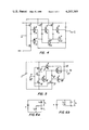
- FIG. 1 illustrates a 1/2 voltage dropping circuit of the present invention
- FIG. 2 illustrates a wave form chart
- FIG. 3 illustrates a 1/3 voltage dropping circuit of the present invention
- FIG. 4 illustrates a 1/4 voltage dropping circuit of the present invention.
- FIG. 5 illustrates a 2/3 voltage dropping circuit according to the present invention
- FIGS. 6a and 6b are schematic diagrams for explaining the operation of the circuit shown in FIG. 1;
- FIG. 7 illustrates a 3/4 voltage dropping circuit according to the present invention
- FIG. 8 illustrates a 3/5 voltage dropping circuit according to the present invention.
- the present invention relates to a voltage dropping circuit which drops the voltage of a power source without power loss.
- FIG. 1 shows a preferable embodiment of the present invention.
- the reference number 1 shows a battery, and the higher voltage terminal of the battery is connected to the source of a P-type MOS-FET 2 and to one side of electrodes of a capacitor 7, respectively. While, the lower voltage terminal of the battery 1 is connected to the source electrode of a N-type MOS-FET 3.
- the drain electrode of the P-type MOS-FET 2 is connected to one side of electrodes of a capacitor 4 and to one of the drain electrodes of a transmission gate (which will be refered to as T.G hereinafter) 5.
- the drain electrode of the N-type MOS-FET 3 is connected to the other side of the electrodes of the capacitor 4 and to one of the drain electrodes of a T.G 6.
- each gate electrode of the P-type MOS-FET 2 and the N-type MOS-FET 3 is connected to the other, and a clock signal ⁇ is applied to both of the gate electrodes.
- the other drain electrode of the T.G 5 is connected to the other drain electrode of the T.G 5 and T.G 6 are connected to the other side of the electrode of the capacitor 7 and also to an output terminal V o .
- the T.G 5 is composed of a P-type MOS-FET and N-type MOS-FET, and clock signals ⁇ and ⁇ are applied to each gate electrode of these MOS-FETs, respectively.
- the T.G 6 is also composed of a P-type MOS-FET and a N-type MOS-FET, and clock signals ⁇ and ⁇ are applied to each gate electrode of these MOS-FETs.
- the voltage of the battery is divided into a half by these two capacitors, and the potential V o will be about a half of E.
- the capacitors 4 and 7 are to be connected in parallel between the higher potential point of the battery and the terminal V o .
- the potential at the terminal V o will become the value of a half of E.
- the circuit since it is possible to drop the circuit output voltage to approximately one half the voltage of the battery without any power loss as well as to easily apply the circuit to an integrated circuit, the circuit can be incorporated in a small size apparatus, such as watch.
- the circuit according to the present invention is effective for use as the power source of a logic element which operates with the voltage value of approximately 0.6 V, such as a multiplex driver of a liquid crystal device, a reference power source for color display, IIL, B-MOS and like, and the circuit of the invention is very effective.
- An output voltage reduced to 1/N of the power source voltage can also be obtained in using N capacitors by the circuit according to the present invention.
- the switching elements are not limitted to the MOS-FETs.
- the present invention is also applicable to a 1/3 voltage dropping circuit shown in FIG. 3, and/or a 1/4 voltage dropping circuit shown in FIG. 4 in addition to the 1/2 voltage dropping circuit.
- FIG. 5 shows a preferable embodiment of a circuit for dropping the voltage to two-third of the source voltage, according to the present invention.
- the reference numeral 1 shows a power source, wherein the higher potential point of power source is connected to the source of a P-type MOS-FET 2 and to one side of the electrodes of a capacitor 11, and the lower potential point of the power source is connected to the source electrodes on N-type MOS-FET 4 and 7, respectively.
- the gate electrode of the P-type MOS-FET 2 is connected to an input terminal 12 to which a clock signal is applied, and the drain electrode of the MOS-FET 2 is connected to one side of the terminals of a capacitor 3 and to one of the input terminals of a transmission gate 5.
- the gate electrode of the N-type MOS-FET 4 is connected to the input terminal 12, and the drain electrode of the MOS-FET 4 is connected to the other side of the terminals of the capacitor 3 and to one of the input terminals of a transmission gate 6, respectively.
- the gate of the N-type MOS-FET 7 is connected to the input terminal 12, the drain of the MOS-FET 7 is connected to one side of terminals of a capacitor 8 and to one of the input terminals of a transmission gate 10.
- the other side of the terminals of the capacitor 8 is connected to the other input of the transmission gate 6 and one of the inputs of a transmission gate 9, respectively.
- the other inputs of the transmission gate 5, 9 and 10 are connected to one side of the terminals of a capacitor 11 and 2/3E output terminal 13, respectively.
- FIG. 6(a) the equivalent circuit in above mentioned status is shown. From this figure, it will be understood that when each value of three capacitors is equal to one another, V o is equal to two-third of E, the voltage of two-third of E is produced across a capacitor C 1 , and the voltage of two-third of E is produced across each of capacitors C 2 and C 3 , respectively.
- the charge which is supplied to the load from the capacitor C 1 in the status shown in FIG. 2(a) is replenished from capacitors C 2 and C 3 in the status shown in FIG. 2(b).
- FIG. 7 shows the embodiment of a 3/4 voltage dropping circuit.
- the circuit of the present invention is easily applicable to an integrated circuit. Therefore, the circuit according to the present invention is extremely suitable for the voltage dropping circuit of a electronic watch or the like.
- the circuit according to the present invention is very effective for use as a power source of a multiplex driver of a liquid crystal device, a power source of elements which operate with the voltage of less than 1.5 V, such as B-MOS, IIL or the like.
- the MOS-FETs and the transmission gates are used for the electronic switches.
- the switching devices are not limited to these devices.
- FIG. 8 The embodiment of a 3/5 voltage dropping circuit is shown in FIG. 8.
Abstract
This invention provides a voltage dropping circuit which is composed of capacitors and MOS field effect electronic switching elements whereby a voltage equal to M/N of the voltage of a power source is obtained.
Description
In the prior art to drop the voltage of a power source, various circuit are used, such as a resistor dividing circuit, a circuit utilizing the voltage drop between the collector and the emitter of a transistor, and a DC-DC converter circuit. These circuits have large size and a power loss, and therefore, these conventional circuits are not suitable for incorporation in small equipment.
The present invention aims to eliminate the above noted difficulty and insufficiency, and the object of the present invention is to provide a lower power consumption voltage dropping circuit which can be incorporated in very small size equipment such as an electronic watch.
The above mentioned and further objects, features and advantages of the present invention will become more apparent from the following description when taken in connection with the accompanying drawings, which show preferred embodiments of the present invention and wherein:
FIG. 1 illustrates a 1/2 voltage dropping circuit of the present invention;
FIG. 2 illustrates a wave form chart;
FIG. 3 illustrates a 1/3 voltage dropping circuit of the present invention; and
FIG. 4 illustrates a 1/4 voltage dropping circuit of the present invention.
FIG. 5 illustrates a 2/3 voltage dropping circuit according to the present invention;
FIGS. 6a and 6b are schematic diagrams for explaining the operation of the circuit shown in FIG. 1;
FIG. 7 illustrates a 3/4 voltage dropping circuit according to the present invention;
FIG. 8 illustrates a 3/5 voltage dropping circuit according to the present invention.
The present invention relates to a voltage dropping circuit which drops the voltage of a power source without power loss.
FIG. 1 shows a preferable embodiment of the present invention. The reference number 1 shows a battery, and the higher voltage terminal of the battery is connected to the source of a P-type MOS-FET 2 and to one side of electrodes of a capacitor 7, respectively. While, the lower voltage terminal of the battery 1 is connected to the source electrode of a N-type MOS-FET 3.
The drain electrode of the P-type MOS-FET 2 is connected to one side of electrodes of a capacitor 4 and to one of the drain electrodes of a transmission gate (which will be refered to as T.G hereinafter) 5. The drain electrode of the N-type MOS-FET 3 is connected to the other side of the electrodes of the capacitor 4 and to one of the drain electrodes of a T.G 6. Furthermore, each gate electrode of the P-type MOS-FET 2 and the N-type MOS-FET 3 is connected to the other, and a clock signal φ is applied to both of the gate electrodes. The other drain electrode of the T.G 5 is connected to the other drain electrode of the T.G 5 and T.G 6 are connected to the other side of the electrode of the capacitor 7 and also to an output terminal Vo.
The T.G 5 is composed of a P-type MOS-FET and N-type MOS-FET, and clock signals φ and φ are applied to each gate electrode of these MOS-FETs, respectively. The T.G 6 is also composed of a P-type MOS-FET and a N-type MOS-FET, and clock signals φ and φ are applied to each gate electrode of these MOS-FETs. When the clock signal φ is at an "H" or "High" level, the T.G 5 is on, and when the clock signal φ is at an "L" or "Low" level, the T.G 6 is off.
Next, the operation of the circuit having the structure described above will be explained hereinafter. When the clock signal φ is at the "H" level, the N-type MOS-FET 3 and the T.G 5 are on, respectively, and the P-type MOS-FET 2 and the T.G 6 are off, respectively. As a result, it follows that the capacitors 7 and 4 have been connected to the battery E in series.
If the value of the capacitor 7 is equal to that of the capacitor 4, the voltage of the battery is divided into a half by these two capacitors, and the potential Vo will be about a half of E.
Next, when the clock signal φ becomes the "L" level condition, the P-type MOS-FET 2 and T.G 6 will be turned on, and the N-type MOS-FET 3 and T.G 5 will be turned off.
Therefore, the capacitors 4 and 7 are to be connected in parallel between the higher potential point of the battery and the terminal Vo. As the result, the potential at the terminal Vo will become the value of a half of E.
Again, when the clock signal φ becomes the "H" level condition, the above-mentioned operation is carried out respeatedly. As a result, approximately 1/2 voltage of that of the battery can always be obtained from the terminal Vo.
The state of the operation is shown in FIG. 2 by wave forms.
As mentioned above, according to the present invention, since it is possible to drop the circuit output voltage to approximately one half the voltage of the battery without any power loss as well as to easily apply the circuit to an integrated circuit, the circuit can be incorporated in a small size apparatus, such as watch.
The circuit according to the present invention is effective for use as the power source of a logic element which operates with the voltage value of approximately 0.6 V, such as a multiplex driver of a liquid crystal device, a reference power source for color display, IIL, B-MOS and like, and the circuit of the invention is very effective.
An output voltage reduced to 1/N of the power source voltage can also be obtained in using N capacitors by the circuit according to the present invention. The switching elements are not limitted to the MOS-FETs. Moreover, the present invention is also applicable to a 1/3 voltage dropping circuit shown in FIG. 3, and/or a 1/4 voltage dropping circuit shown in FIG. 4 in addition to the 1/2 voltage dropping circuit.
FIG. 5 shows a preferable embodiment of a circuit for dropping the voltage to two-third of the source voltage, according to the present invention. The reference numeral 1 shows a power source, wherein the higher potential point of power source is connected to the source of a P-type MOS-FET 2 and to one side of the electrodes of a capacitor 11, and the lower potential point of the power source is connected to the source electrodes on N-type MOS-FET 4 and 7, respectively.
The gate electrode of the P-type MOS-FET 2 is connected to an input terminal 12 to which a clock signal is applied, and the drain electrode of the MOS-FET 2 is connected to one side of the terminals of a capacitor 3 and to one of the input terminals of a transmission gate 5. The gate electrode of the N-type MOS-FET 4 is connected to the input terminal 12, and the drain electrode of the MOS-FET 4 is connected to the other side of the terminals of the capacitor 3 and to one of the input terminals of a transmission gate 6, respectively.
The gate of the N-type MOS-FET 7 is connected to the input terminal 12, the drain of the MOS-FET 7 is connected to one side of terminals of a capacitor 8 and to one of the input terminals of a transmission gate 10. The other side of the terminals of the capacitor 8 is connected to the other input of the transmission gate 6 and one of the inputs of a transmission gate 9, respectively. The other inputs of the transmission gate 5, 9 and 10 are connected to one side of the terminals of a capacitor 11 and 2/3E output terminal 13, respectively.
Next, the operation of the circuit which is constructed as described above will be explained hereinafter. When a clock φ is at an "H" level, the N-type MOS-FET 4, the N-type MOS-FET 7, the transmission gate 5 and the transmission gate 9 are on, respectively, and the transmission gate 6 and 10 are off.
In FIG. 6(a), the equivalent circuit in above mentioned status is shown. From this figure, it will be understood that when each value of three capacitors is equal to one another, Vo is equal to two-third of E, the voltage of two-third of E is produced across a capacitor C1, and the voltage of two-third of E is produced across each of capacitors C2 and C3, respectively.
Next, when clock φ becomes an "L" level, the P-type MOS-FET 2, the transmission gate 6 and the transmission gate 10 will be turned on while the N-type MOS-FET 4, the N-type MOS-FET 7, the transmission gate 5 and the transmission gate 9 will be turned off.
The equivalent circuit in the above mentioned case is shown in FIG. 6(b). Since the capacitors C2 and C3 each of which has the charge corresponding to the voltage of one-third of E is connected to each other in series, the output Vo ' will also become two-third of E.
The charge which is supplied to the load from the capacitor C1 in the status shown in FIG. 2(a) is replenished from capacitors C2 and C3 in the status shown in FIG. 2(b).
FIG. 7 shows the embodiment of a 3/4 voltage dropping circuit.
As described above, according to the present invention, it is possible to drop the voltage of the power source without any power loss. Furthermore, the circuit of the present invention is easily applicable to an integrated circuit. Therefore, the circuit according to the present invention is extremely suitable for the voltage dropping circuit of a electronic watch or the like. The circuit according to the present invention is very effective for use as a power source of a multiplex driver of a liquid crystal device, a power source of elements which operate with the voltage of less than 1.5 V, such as B-MOS, IIL or the like.
In the embodiment described above, the MOS-FETs and the transmission gates are used for the electronic switches. However, the switching devices are not limited to these devices.
Also, in the same way, it is possible to obtain a desired voltage dropping ratio in addition to the ratio of (n-1)/n by adjusting the value of the capacitors.
The embodiment of a 3/5 voltage dropping circuit is shown in FIG. 8.
Claims (3)
1. A voltage dropping circuit, comprising: a first MOS field effect transistor, a first capacitor and a second MOS field effect transistor connected in series in the named order; a first MOS field effect transmission gate responsive to control signals of opposite polarity and rendered conductive by a control signal of either polarity and a second capacitor connected in series with said first transmission gate, wherein the series combination of said first transmission gate and said second capacitor are connected in parallel with said first MOS field effect transistor with said first transmission gate connected to a junction of said first MOS field effect transistor and said first capacitor; a second MOS field effect transmission gate responsive to control signals of opposite polarity and rendered conductive by a control signal of either polarity and connected between a junction of said second capacitor and said first transmission gate and a junction of said first capacitor and said second MOS field effect transistor; means for applying a first control signal to respective gates of said first and second MOS field effect transistors and to said first and second transmission gates so as to render one transmission gate conductive and the other transmission gate non-conductive; and means for applying a second control signal to said first and second transmission gates so as to render one transmission gate conductive and the other transmission gate non-conductive.
2. A voltage dropping circuit according to claim 1; wherein said first and second MOS field effect transistors have opposite channel polarity.
3. A voltage dropping circuit according to claim 1, further comprising: a voltage source connected across the series combination of said first and second MOS field effect transistors and said first capacitor; and means defining an output terminal at said junction of said second capacitor and said first transmission gate; wherein the first control signal is effective for flowing a current from said voltage source to charge said first and second capacitors in series and develop an output voltage at said output terminal, and the second control signal is effective for electrically connecting said first and second capacitors in parallel and the parallel combination of said first and second capacitors in series with said voltage source and develop an output voltage at said output terminal.
Applications Claiming Priority (4)
| Application Number | Priority Date | Filing Date | Title |
|---|---|---|---|
| JP1591677A JPS53101616A (en) | 1977-02-16 | 1977-02-16 | Step-down cirucit |
| JP52-15916 | 1977-02-16 | ||
| JP52-34186 | 1977-03-28 | ||
| JP3418677A JPS53118724A (en) | 1977-03-28 | 1977-03-28 | Step-down circuit |
Publications (1)
| Publication Number | Publication Date |
|---|---|
| US4205369A true US4205369A (en) | 1980-05-27 |
Family
ID=26352150
Family Applications (1)
| Application Number | Title | Priority Date | Filing Date |
|---|---|---|---|
| US05/876,369 Expired - Lifetime US4205369A (en) | 1977-02-16 | 1978-02-09 | Voltage dropping circuit |
Country Status (1)
| Country | Link |
|---|---|
| US (1) | US4205369A (en) |
Cited By (18)
| Publication number | Priority date | Publication date | Assignee | Title |
|---|---|---|---|---|
| EP0075129A2 (en) * | 1981-08-27 | 1983-03-30 | Kabushiki Kaisha Toshiba | Voltage dropping or voltage increasing electronic circuit |
| US4433282A (en) * | 1981-12-08 | 1984-02-21 | Intersil | Monolithic voltage divider |
| US4451743A (en) * | 1980-12-29 | 1984-05-29 | Citizen Watch Company Limited | DC-to-DC Voltage converter |
| US4460953A (en) * | 1981-05-08 | 1984-07-17 | Hitachi, Ltd. | Signal voltage dividing circuit |
| US4578772A (en) * | 1981-09-18 | 1986-03-25 | Fujitsu Limited | Voltage dividing circuit |
| US4730122A (en) * | 1986-09-18 | 1988-03-08 | International Business Machines Corporation | Power supply adapter systems |
| US4868908A (en) * | 1988-10-18 | 1989-09-19 | Ventritex | Power supply down-conversion, regulation and low battery detection system |
| US4952864A (en) * | 1988-10-18 | 1990-08-28 | Ventritex | Power supply down-conversion, regulation and low battery detection system |
| EP0585925A2 (en) * | 1992-09-02 | 1994-03-09 | Nec Corporation | Voltage converting circuit and multiphase clock generating circuit used for driving the same |
| US5345376A (en) * | 1993-02-19 | 1994-09-06 | Tescom Corporation | Switching power supply with electronic isolation |
| US5850337A (en) * | 1997-07-25 | 1998-12-15 | Lucent Technologies Inc. | Magnetic-free DC/DC converter and method of operation thereof |
| EP0960469A1 (en) * | 1997-02-11 | 1999-12-01 | The Foxboro Company | Charged pump for dividing input voltage and multiplying output current |
| US6198645B1 (en) | 1998-07-02 | 2001-03-06 | National Semiconductor Corporation | Buck and boost switched capacitor gain stage with optional shared rest state |
| WO2001050812A1 (en) * | 2000-01-07 | 2001-07-12 | Widex A/S | A digital hearing aid with a voltage converter |
| US6317634B1 (en) | 1999-04-30 | 2001-11-13 | Cardiac Pacemakers, Inc. | Implantable cardiac stimulating device with optimized demand |
| US6421262B1 (en) | 2000-02-08 | 2002-07-16 | Vlt Corporation | Active rectifier |
| US7456677B1 (en) * | 2006-05-01 | 2008-11-25 | National Semiconductor Corporation | Fractional gain circuit with switched capacitors and smoothed gain transitions for buck voltage regulation |
| US9735682B1 (en) * | 2016-03-15 | 2017-08-15 | Kabushiki Kaisha Toshiba | Step-down circuit |
Citations (5)
| Publication number | Priority date | Publication date | Assignee | Title |
|---|---|---|---|---|
| US3478258A (en) * | 1967-05-24 | 1969-11-11 | Sony Corp | Transformerless voltage reducing rectifier circuit |
| US3505586A (en) * | 1968-02-27 | 1970-04-07 | Int Rectifier Corp | Transformerless high-current power supply |
| US3708742A (en) * | 1971-06-30 | 1973-01-02 | Ibm | High dc to low dc voltage converter |
| DE2558656A1 (en) * | 1975-12-30 | 1977-07-07 | Stellar Radiation Variable Lic | Voltage halving circuit with two series capacitors - has capacitors discharged alternately into output capacitor by two transistor switches |
| US4061929A (en) * | 1975-09-22 | 1977-12-06 | Kabushiki Kaisha Daini Seikosha | Circuit for obtaining DC voltage higher than power source voltage |
-
1978
- 1978-02-09 US US05/876,369 patent/US4205369A/en not_active Expired - Lifetime
Patent Citations (5)
| Publication number | Priority date | Publication date | Assignee | Title |
|---|---|---|---|---|
| US3478258A (en) * | 1967-05-24 | 1969-11-11 | Sony Corp | Transformerless voltage reducing rectifier circuit |
| US3505586A (en) * | 1968-02-27 | 1970-04-07 | Int Rectifier Corp | Transformerless high-current power supply |
| US3708742A (en) * | 1971-06-30 | 1973-01-02 | Ibm | High dc to low dc voltage converter |
| US4061929A (en) * | 1975-09-22 | 1977-12-06 | Kabushiki Kaisha Daini Seikosha | Circuit for obtaining DC voltage higher than power source voltage |
| DE2558656A1 (en) * | 1975-12-30 | 1977-07-07 | Stellar Radiation Variable Lic | Voltage halving circuit with two series capacitors - has capacitors discharged alternately into output capacitor by two transistor switches |
Cited By (33)
| Publication number | Priority date | Publication date | Assignee | Title |
|---|---|---|---|---|
| US4451743A (en) * | 1980-12-29 | 1984-05-29 | Citizen Watch Company Limited | DC-to-DC Voltage converter |
| US4460953A (en) * | 1981-05-08 | 1984-07-17 | Hitachi, Ltd. | Signal voltage dividing circuit |
| EP0075129A2 (en) * | 1981-08-27 | 1983-03-30 | Kabushiki Kaisha Toshiba | Voltage dropping or voltage increasing electronic circuit |
| EP0075129A3 (en) * | 1981-08-27 | 1984-03-28 | Tokyo Shibaura Denki Kabushiki Kaisha | Voltage dropping electronic circuit |
| US4485432A (en) * | 1981-08-27 | 1984-11-27 | Tokyo Shibaura Denki Kabushiki Kaisha | Electronic voltage drop circuit |
| US4578772A (en) * | 1981-09-18 | 1986-03-25 | Fujitsu Limited | Voltage dividing circuit |
| US4433282A (en) * | 1981-12-08 | 1984-02-21 | Intersil | Monolithic voltage divider |
| US4730122A (en) * | 1986-09-18 | 1988-03-08 | International Business Machines Corporation | Power supply adapter systems |
| US4868908A (en) * | 1988-10-18 | 1989-09-19 | Ventritex | Power supply down-conversion, regulation and low battery detection system |
| US4952864A (en) * | 1988-10-18 | 1990-08-28 | Ventritex | Power supply down-conversion, regulation and low battery detection system |
| EP0585925A2 (en) * | 1992-09-02 | 1994-03-09 | Nec Corporation | Voltage converting circuit and multiphase clock generating circuit used for driving the same |
| EP0585925A3 (en) * | 1992-09-02 | 1995-01-18 | Nippon Electric Co | Voltage converting circuit and multiphase clock generating circuit used for driving the same. |
| US5461557A (en) * | 1992-09-02 | 1995-10-24 | Nec Corporation | Voltage converting circuit and multiphase clock generating circuit used for driving the same |
| US5532916A (en) * | 1992-09-02 | 1996-07-02 | Nec Corporation | Voltage converting circuit and multiphase clock generating circuit used for driving the same |
| US5623222A (en) * | 1992-09-02 | 1997-04-22 | Nec Corporation | Voltage converting circuit and multiphase clock generating circuit used for driving the same |
| US5345376A (en) * | 1993-02-19 | 1994-09-06 | Tescom Corporation | Switching power supply with electronic isolation |
| EP0960469A4 (en) * | 1997-02-11 | 2000-09-27 | Foxboro Co | Charged pump for dividing input voltage and multiplying output current |
| EP0960469A1 (en) * | 1997-02-11 | 1999-12-01 | The Foxboro Company | Charged pump for dividing input voltage and multiplying output current |
| US5850337A (en) * | 1997-07-25 | 1998-12-15 | Lucent Technologies Inc. | Magnetic-free DC/DC converter and method of operation thereof |
| US6198645B1 (en) | 1998-07-02 | 2001-03-06 | National Semiconductor Corporation | Buck and boost switched capacitor gain stage with optional shared rest state |
| US20020120302A1 (en) * | 1999-04-30 | 2002-08-29 | Cardiac Pacemakers, Inc. | Implantable cardiac stimulating device with optimized demand |
| US6317634B1 (en) | 1999-04-30 | 2001-11-13 | Cardiac Pacemakers, Inc. | Implantable cardiac stimulating device with optimized demand |
| US6353760B1 (en) | 1999-04-30 | 2002-03-05 | Cardiac Pacemakers, Inc. | Implantable cardiac stimulating device with optimized demand |
| US6363283B1 (en) | 1999-04-30 | 2002-03-26 | Cardiac Pacemakers, Inc. | Implantable cardiac stimulating device with optimized demand |
| US6892096B2 (en) | 1999-04-30 | 2005-05-10 | Cardiac Pacemakers, Inc. | Implantable cardiac stimulating device with optimized demand |
| WO2001050812A1 (en) * | 2000-01-07 | 2001-07-12 | Widex A/S | A digital hearing aid with a voltage converter |
| AU768987B2 (en) * | 2000-01-07 | 2004-01-15 | Widex A/S | A digital hearing aid with a voltage converter |
| US6741715B2 (en) | 2000-01-07 | 2004-05-25 | Widex A/S | Digital hearing aid with a voltage converter for supplying a reduced operation voltage |
| US6421262B1 (en) | 2000-02-08 | 2002-07-16 | Vlt Corporation | Active rectifier |
| US20020163322A1 (en) * | 2000-02-08 | 2002-11-07 | Vlt Corporation, A Texas Corporation | Active rectifier |
| US7015561B2 (en) | 2000-02-08 | 2006-03-21 | Vlt, Inc. | Active rectifier |
| US7456677B1 (en) * | 2006-05-01 | 2008-11-25 | National Semiconductor Corporation | Fractional gain circuit with switched capacitors and smoothed gain transitions for buck voltage regulation |
| US9735682B1 (en) * | 2016-03-15 | 2017-08-15 | Kabushiki Kaisha Toshiba | Step-down circuit |
Similar Documents
| Publication | Publication Date | Title |
|---|---|---|
| US4205369A (en) | Voltage dropping circuit | |
| US3975671A (en) | Capacitive voltage converter employing CMOS switches | |
| US4068295A (en) | Voltage multiplier for an electronic time apparatus | |
| US4029973A (en) | Voltage booster circuit using level shifter composed of two complementary MIS circuits | |
| US3824447A (en) | Booster circuit | |
| EP0585925B1 (en) | Voltage converting circuit | |
| EP0079496B1 (en) | Matrix display and driving method therefor | |
| US4045691A (en) | Level shift circuit | |
| JPH03235517A (en) | Switching circuit | |
| US4796174A (en) | Direct voltage multiplier capable of being integrated into a semiconducting structure | |
| US4176289A (en) | Driving circuit for integrated circuit semiconductor memory | |
| US4229668A (en) | Transistor circuit having a plurality of CMOS circuits | |
| KR950001084B1 (en) | Integrated logic circuit | |
| US4070600A (en) | High voltage driver circuit | |
| US4324991A (en) | Voltage selector circuit | |
| US4124806A (en) | Electronic device for the production of signals of an amplitude greater than the amplitude of a given periodic signal | |
| US5465069A (en) | Interface circuit and voltage-raising circuit including such a circuit | |
| GB1330679A (en) | Tri-level voltage generator circuit | |
| JPH09148913A (en) | High potential difference level shift circuit | |
| CA1132192A (en) | Voltage converter circuit | |
| US4656574A (en) | Logic signal multiplier circuit | |
| GB957043A (en) | Electronic semi-conductor device comprising a bistable electric circuit | |
| US5467048A (en) | Semiconductor device with two series-connected complementary misfets of same conduction type | |
| US4454431A (en) | Semiconductor circuit with a circuit part controlled by a substrate bias | |
| US4404477A (en) | Detection circuit and structure therefor |