US4260951A - Measurement system having pole zero cancellation - Google Patents
Measurement system having pole zero cancellation Download PDFInfo
- Publication number
- US4260951A US4260951A US06/006,983 US698379A US4260951A US 4260951 A US4260951 A US 4260951A US 698379 A US698379 A US 698379A US 4260951 A US4260951 A US 4260951A
- Authority
- US
- United States
- Prior art keywords
- pulse
- current
- coupled
- cancellation
- voltage
- Prior art date
- Legal status (The legal status is an assumption and is not a legal conclusion. Google has not performed a legal analysis and makes no representation as to the accuracy of the status listed.)
- Expired - Lifetime
Links
- 238000005259 measurement Methods 0.000 title description 3
- 230000036772 blood pressure Effects 0.000 claims abstract description 17
- 238000007493 shaping process Methods 0.000 claims abstract description 9
- 239000003990 capacitor Substances 0.000 claims description 55
- 238000012545 processing Methods 0.000 claims description 6
- 238000012546 transfer Methods 0.000 claims description 6
- 238000009532 heart rate measurement Methods 0.000 abstract description 9
- 230000000694 effects Effects 0.000 abstract description 8
- 230000004069 differentiation Effects 0.000 description 37
- 238000010586 diagram Methods 0.000 description 22
- 230000001360 synchronised effect Effects 0.000 description 17
- 230000004044 response Effects 0.000 description 15
- 230000006870 function Effects 0.000 description 14
- 230000003750 conditioning effect Effects 0.000 description 12
- 238000005070 sampling Methods 0.000 description 8
- 230000035488 systolic blood pressure Effects 0.000 description 8
- 230000005540 biological transmission Effects 0.000 description 7
- 230000008859 change Effects 0.000 description 6
- 230000008878 coupling Effects 0.000 description 6
- 238000010168 coupling process Methods 0.000 description 6
- 238000005859 coupling reaction Methods 0.000 description 6
- 230000003321 amplification Effects 0.000 description 4
- 238000001914 filtration Methods 0.000 description 4
- 230000010354 integration Effects 0.000 description 4
- 238000003199 nucleic acid amplification method Methods 0.000 description 4
- 230000031700 light absorption Effects 0.000 description 3
- 238000011084 recovery Methods 0.000 description 3
- 230000009471 action Effects 0.000 description 2
- 230000035559 beat frequency Effects 0.000 description 2
- 230000008901 benefit Effects 0.000 description 2
- 238000006243 chemical reaction Methods 0.000 description 2
- 239000013078 crystal Substances 0.000 description 2
- 230000003247 decreasing effect Effects 0.000 description 2
- 238000006073 displacement reaction Methods 0.000 description 2
- 230000005669 field effect Effects 0.000 description 2
- 238000000034 method Methods 0.000 description 2
- 238000012986 modification Methods 0.000 description 2
- 230000004048 modification Effects 0.000 description 2
- 230000003071 parasitic effect Effects 0.000 description 2
- 230000002093 peripheral effect Effects 0.000 description 2
- 230000035945 sensitivity Effects 0.000 description 2
- 230000006641 stabilisation Effects 0.000 description 2
- 238000011105 stabilization Methods 0.000 description 2
- 230000000087 stabilizing effect Effects 0.000 description 2
- 230000015572 biosynthetic process Effects 0.000 description 1
- 239000002131 composite material Substances 0.000 description 1
- 238000012937 correction Methods 0.000 description 1
- 230000000994 depressogenic effect Effects 0.000 description 1
- 238000001514 detection method Methods 0.000 description 1
- 238000011161 development Methods 0.000 description 1
- 230000003205 diastolic effect Effects 0.000 description 1
- 230000006872 improvement Effects 0.000 description 1
- 238000002955 isolation Methods 0.000 description 1
- 238000012332 laboratory investigation Methods 0.000 description 1
- 238000012544 monitoring process Methods 0.000 description 1
- 239000002245 particle Substances 0.000 description 1
- 230000035515 penetration Effects 0.000 description 1
- 238000002310 reflectometry Methods 0.000 description 1
- 230000000284 resting effect Effects 0.000 description 1
- 238000012552 review Methods 0.000 description 1
- 230000033764 rhythmic process Effects 0.000 description 1
- 239000000758 substrate Substances 0.000 description 1
- 238000003786 synthesis reaction Methods 0.000 description 1
- 238000012360 testing method Methods 0.000 description 1
- 230000007704 transition Effects 0.000 description 1
Images


Classifications
-
- A—HUMAN NECESSITIES
- A61—MEDICAL OR VETERINARY SCIENCE; HYGIENE
- A61B—DIAGNOSIS; SURGERY; IDENTIFICATION
- A61B5/00—Measuring for diagnostic purposes; Identification of persons
- A61B5/02—Detecting, measuring or recording pulse, heart rate, blood pressure or blood flow; Combined pulse/heart-rate/blood pressure determination; Evaluating a cardiovascular condition not otherwise provided for, e.g. using combinations of techniques provided for in this group with electrocardiography or electroauscultation; Heart catheters for measuring blood pressure
- A61B5/024—Detecting, measuring or recording pulse rate or heart rate
- A61B5/02438—Detecting, measuring or recording pulse rate or heart rate with portable devices, e.g. worn by the patient
-
- A—HUMAN NECESSITIES
- A61—MEDICAL OR VETERINARY SCIENCE; HYGIENE
- A61B—DIAGNOSIS; SURGERY; IDENTIFICATION
- A61B5/00—Measuring for diagnostic purposes; Identification of persons
- A61B5/02—Detecting, measuring or recording pulse, heart rate, blood pressure or blood flow; Combined pulse/heart-rate/blood pressure determination; Evaluating a cardiovascular condition not otherwise provided for, e.g. using combinations of techniques provided for in this group with electrocardiography or electroauscultation; Heart catheters for measuring blood pressure
- A61B5/024—Detecting, measuring or recording pulse rate or heart rate
- A61B5/02416—Detecting, measuring or recording pulse rate or heart rate using photoplethysmograph signals, e.g. generated by infrared radiation
- A61B5/02427—Details of sensor
- A61B5/02433—Details of sensor for infrared radiation
-
- A—HUMAN NECESSITIES
- A61—MEDICAL OR VETERINARY SCIENCE; HYGIENE
- A61B—DIAGNOSIS; SURGERY; IDENTIFICATION
- A61B5/00—Measuring for diagnostic purposes; Identification of persons
- A61B5/72—Signal processing specially adapted for physiological signals or for diagnostic purposes
- A61B5/7235—Details of waveform analysis
- A61B5/7239—Details of waveform analysis using differentiation including higher order derivatives
Definitions
- a photodiode is connected directly to a signal conditioning circuit which rapidly removes unwanted asynchronous ambient background light signals such as from sunlight, by means of a switched ambient light subtractor circuit.
- the signal current after cancellation of the ambient background signal is sampled in an integrate and hold circuit to provide a heart systolic pressure wave or envelope of the pulse amplitudes.
- the synchronous steady state IR pulse carrier envelope signal is cancelled by a perfect second-order feedback loop via an integrating amplifier and a switched transconductance element that operates with fast response, even under conditions of large overloads that occur at the sensor.
- the second-order feedback loop because of various restraints, necessarily has a long differentiation time constant.
- the pole zero cancellation circuit which is included in an amplifier circuit cancels the long differentiation time constant so as to remove undesired shaping of the heart pressure wave caused by the second-order loop.
- a heart pressure wave which has been shaped by a double differentiation with only a short time constant is provided at the output of the amplifier circuit. Pulses of the heart systolic pressure wave are then detected with a high degree of timing accuracy to determine the pulse rate which is then displayed.
- This invention is related to pulse rate measurement systems, and particularly to an improved pulse rate measuring system that includes input coupled pole zero cancellation to rapidly and accurately develop pulse rate readings.
- a pulsed IR plethysmograph having a photodiode and a gated circuit connected thereto for pulse-by-pulse cancellation of the asynchronous ambient light components of the photocurrent signal.
- a switched integrate and hold circuit was provided to respond to the current signal after ambient light cancellation to provide a signal representive of the blood pressure modulation.
- a switching transconductance element, an integrating operational amplifier and the integrate and hold circuit were included in a perfect second-order feedback loop to develop current pulses for cancellation of synchronous IR carrier steady state photocurrent resulting from the pulsed light source.
- Pole zero cancellation is generally known in network theory, at least as to remaining poles at the limits, as discussed in the book by E. A. Guillermin, Synthesis of Passive Networks, John Wiley and Sons, Inc., New York, 1957. Also, in the nuclear field, pole zero cancellation has been applied to some of the problems of pulse shaping in nuclear pulse amplifiers, as discussed in a paper by C. H. Nowlen and J. L. Blankenship published starting with page 1830 in the Review of Scientific Instruments, 1965 edition, Vol. 36, No. 12. This paper shows a system operating with a charge sensitive preamplifier that has overload conditions resulting from high energy particles that deposit a large amount of energy on the detector causing the charge sensitive preamplifier to go into an overload condition.
- pole zero cancellation in in the system of the paper is to cancel the effect of the slow recovery of the charge sensitive preamplifier so that information can be reliably extracted from a single pulse.
- the objective of applicant's compensation by pole zero cancellation is different than taught in the prior art in that Applicant's system operates with DC coupling to a perfect second-order loop which has the purposes of suppressing the individual pulse of the pulse carrier and extracting only the information from variations in pulse-to-pulse amplitude.
- Applicant's compensation operates in a time frame that is slow compared to the pulse-to-pulse time interval.
- the nuclear pulse amplifier system of the paper uses pole zero cancellation to discard the remnants of a pressure pulse so that the system is totally cleaned when the next pulse is received.
- Applicant's invention is to prevent excess noise and an undesirable shaping effect in the heart blood pressure wave which would lead to improper timing information while the pole zero cancellation in the paper is used primarily for measuring pulse amplitude rather than time. Accordingly, Applicant's type of compensating circuit including its function, is direct coupling to the signal source and its arrangement in conjunction with a perfect second-order loop input is not taught in the prior art.
- a pulsed IR reflectance plethysmograph for heart rate measurement includes a signal processing circuit providing a heart pressure wave that is filtered with a differentiation having a relatively large time constant because of the restraints on the component values such as resulting from the chip size in a digital watch.
- a novel amplifier arrangement is directly coupled to the signal processing circuit and includes a pole cancelling arrangement to effectively substitute a short time constant differentiation for the long time constant differentiation.
- two short time constant coupling networks must be used. Triple differentiation produces undesireable signal shaping and signal-to-noise characteristics.
- the input signal processing circuit differentiation must be cancelled and it is simpler to accomplish this if it has a long differentiation time constant rather than a short one.
- the system has a pulsed light source applying the pulses of light to a finger, for example, for reflection to a detector such as a photodiode.
- a gated circuit is connected directly to the photodiode for pulse-by-pulse cancellation of the asynchronous ambient light components of the photocurrent signal.
- a switched integrate and hold circuit is provided to respond to the current signal after ambient light cancellation to develop a signal representative of the blood pressure modulation.
- a perfect second-order loop is formed including the integrate and hold circuit, an integrating operational amplifier and a switched transconductance element, and develops current pulses for cancellation of synchronous IR carrier steady state photocurrent resulting from the pulsed light source.
- the integrating operational amplifier includes a resistor R B and a capacitor C B for providing the differentiation time constant to the system response.
- the amplifier and filter circuit includes an operational amplifier directly coupled to the integrate and hold circuit through a differentiating capacitor and resistor.
- a bypass resistor R 3 is coupled in parallel to the differentiating capacitor C 1 to provide a time constant R 3 C 1 equal to R B C B .
- the bypass resistor R 3 provides a zero to cancel the pole caused by the R B C B differentiation with the result that a short time constant differentiation (R 1 ⁇ R 3 ).C 1 is substituted for the large time constant differentiation.
- the shaped heart wave signal amplifier output has a high degree of systolic pressure wave pulse-to-pulse timing accuracy and a reliable pulse interval can be detected for displaying the pulse rate.
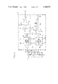
- FIG. 1 is a schematic block diagram of a pulsed IR reflectance plethysmograph system for heart rate measurements illustrated in a wristwatch as an example of one use of the system in accordance with the invention
- FIG. 1a is a schematic circuit and block diagram showing a sensor and the current conditioning section of FIG. 1 in further detail;
- FIG. 2 is a schematic circuit diagram of the asynchronous ambient light cancellation circuit shown in the system of FIGS. 1 and 1a;
- FIG. 3 is a schematic circuit diagram of the switched capacitor transconductance element shown in a perfect second-order feedback loop in the system of FIGS. 1 and 1a for synchronous steady state pulse carrier light cancellation;
- FIG. 4 is a basic logic timing diagram for the system of FIG. 1;
- FIG. 5 is a specific logic timing diagram for the circuits of FIGS. 2 and 3;
- FIG. 6 is a schematic diagram of waveforms of voltage and current as a function of time for further explaining the operation of the system of FIGS. 1 and 1a;
- FIG. 7 is a schematic diagram of voltage as a function of time illustrating a typical systolic blood pressure waveform developed by the signal conditioning circuit (Block 24) and the amplifier and bandpass filter (Block 26) of FIG. 1; and the pulse train that is derived from the threshold disciminator (28) of FIG. 1;
- FIG. 8 is a schematic circuit and block diagram of an amplifier and bandpass filter of FIG. 1 including the pole-zero cancellation system in accordance with the invention
- FIG. 9 is a schematic drawing of diagrams the output to input voltage ratio in decibles as a function of log f for explaining the amplifier and bandpass filter of FIG. 8;
- FIG. 10 is a schematic diagram of waveforms of voltage as a function of time for further explaining the operation of the amplifier and bandpass filter of FIG. 8 with the pole-zero cancellation system in accordance with the invention.
- one embodiment of the invention is incorporated in a plethysmograph adapted to fit in the case of a digital wristwatch for use in field measurements of heart rate, such as by a jogger immediately upon stopping, or while resting, for use by a person who must measure his heart rate frequently, or for use by medical or related personnel.
- a digital wristwatch for use in field measurements of heart rate, such as by a jogger immediately upon stopping, or while resting, for use by a person who must measure his heart rate frequently, or for use by medical or related personnel.
- the principles of the invention are not limited to wristwatches but also apply to instruments that may have other forms such as those that may be desirable for field or hospital uses.
- the illustrated system which includes the compensating combinations of the invention, is a heart rate measurement device which uses the IR reflectometer principle for peripheral pulse measurement by sensing volumetric variations of the capillaries of the fingers or of any tissue with sufficient capiliary development to provide a useful light absorption signal.
- the system in which the invention is incorporated includes operation at any suitable IR or other wavelengths at which there is suitable penetration through tissue to respond to the blood pressure variations and is not be limited to any particular wavelength band.
- the illustrated system utilizes an infrared (IR) light emitting diode (LED) 10 to provide a pulsed source of IR light which is reflected off of the tissues of the finger, for example, and onto a photodiode detector diode 12 having a photocurrent response characteristic.
- IR infrared
- LED light emitting diode
- the peripheral systolic wave causes an abrupt increase in IR light absorption (the reflectance drops) by the capillaries of the finger which dilate in response to the systolic pressure wave.
- the small ( ⁇ 2%) changes or modulation in reflected light amplitude is sensed by the photodiode 12 along with the steady state component of the reflected IR light pulse train plus ambient light from any other source such as sunlight or indoor lighting.
- the LED 10 is driven in an open loop with constant current pulses so that the LED drive and front end gains are therefore set at optimum levels and these levels do not and need not change as a result of beackground lighting conditions or tissue reflectivity.
- the LED 10 is driven at a fixed rate set by timing or clock pulses ⁇ 4 .
- a crystal oscillator and pulse system timing generator 14 provides the timing pulses ⁇ 4 which are typically at 73 Hz (to insure that the beat frequencies between the 73 Hz sampling frequency and the indoor lighting frequencies are well above the system passband) to a base current pulse generator 16, which in turn applies pulses to the base of an NPN type drive transistor Q 1 .
- the emitter of the transistor Q 1 is coupled to a negative supply voltage, -V, and the collector is coupled through a resistor R 1 to the cathode of the LED 10.
- the anode of the LED 10 is coupled through a lead 13 to the positive supply voltage, +V, and to the cathode of the photodiode 12 which in turn has its anode coupled to a lead 15.
- a resistor R 2 is connected to the +V supply (lead 13) and to the lead 15.
- the transistor Q 1 conducts pulses of current through the LED 10 and through the current limiting resistor R 1 when an analog power control signal ⁇ A is turned on.
- a digital watch timing and pulse rated computation section 18 of a digital watch provides the control signal ⁇ A to the timing generator 14 once the operator depresses a push button switch 20. When the switch 20 is depressed a second time, the control signal ⁇ A is then turned off.
- the LED 10 in the illustrated watch system is mounted in a small sensor 22 illustrated as a dotted box on the face of the watch to pass or transmit IR pulses to the surface of a finger 23, for example, of the person whose pulse rate is being monitored.
- the IR pulses reflected off the tissue and capillaries of the finger 23 are received by the photodetector 12, also mounted in the sensor 22.
- the timing generator 14 which responds to a crystal oscillator as is well known in the art, provides the timing signal ⁇ 4 as well as timing signals ⁇ 1 and ⁇ 2 for use in the system. Also, the timing generator 14 applies suitable signals such as a 32 KHz clock signal and 1024 Hz signal to the computation section 18.
- An input signal current conditioning section 24 directly coupled to the photodiode anode through the lead 15, cancels asynchronous ambient light (sunlight, or artificial light as well as other light asynchronous to the system) and synchronous steady state components of the LED light pulse carrier.
- the output of the signal conditioning section 24 passes through a node 25 to an amplifier and bandpass filter 26 as a heart pressure wave voltage having systolic pulses occurring at a rate that is typically 60 to 80 per minute but which can also be as high as 199 pulses per minute.
- the amplifier and bandpass filter 26 includes the compensating arrangement that in combination with the section 24 provides the highly accurate pulse counting system in accordance with the invention.
- the type of computations provided by the section 18 is well known in the digital art and need not be explained in further detail.
- the pulse rate R is then displayed as a decimal number by a digital watch display section 30.
- a suitable power supply such as a battery power supply 31 is provided and may include a pair of batteries (not shown) that together provide a voltage of approximately 3.2 volts between the voltages +V and -V as utilized in the illustrated heart rate monitoring system in a watch.
- the power supply 31 also provides voltages VR 4 , VR 5 and VR G .
- the voltage VR 5 for the discriminator 28 is provided for example, by a series string of five diodes, coupled between +V and a constant current generator source with the voltage VR 5 being provided at the cathode of the diode that is coupled to the constant current source.
- the voltage VR 4 is the voltage at the anode of the last diode that is coupled to the constant current source.
- the discriminator 28 triggers on any signal from the amplifier and bandpass filter 26 that exceeds the difference between the discriminator reference voltage VR 5 and the amplifier quiescent output voltage VR 4 .
- the voltage VR 4 -VR 5 is typically one diode drop or approximately 0.5 volts.
- the input current conditioning section 24 includes an asynchronous ambient light cancellation circuit 32 coupled to the lead 15 to receive a photocurrent i 3 which is a current i 1 as provided by the photodiode 12 (and a small current i 6 from the diode bias resistor R 2 ) combined at a node 41 with the synchronous carrier supression current i 2 .
- the ambient light current cancellation circuit 32 also receives the reference voltage VR G and the timing pulses ⁇ 1 and ⁇ 2 for providing carrier cancellation during the sampling pulse periods, and applies an output current i 5 on a lead 33 to an integrate and hold circuit 34.
- Gates G 3 and G 7 , an integrate and hold capacitor C c and a unity gain amplifier 43 are all included in the integrate and hold circuit 34.
- the gate G 3 responsive to timing signal ⁇ 1 for being biased into conduction is coupled between the lead 33 and a node 37 which in turn is coupled to a positive input terminal of the unity gain amplifier 43.
- the capacitor C c is coupled between a +V terminal and the node 37 to provide integration of the signal for applying a blood pressure wave to the node 25.
- a gate G 7 is coupled between the lead 33 and the negative feedback input terminal of the unity gain amplifier 43, as well as to the node 25.
- the gate G 7 is biased into conduction in response to the timing signal ⁇ 2 to prevent the parasitic capacitance in the circuit at the lead 33 from being charged during the interval between LED pulses.
- a perfect second order feedback loop 39 includes an operational integrator 38, a resistor R A , an integrating capacitor C B , a stabilizing resistor R B , an integrating operational amplifier 42, and includes a switched capacitor transconductance element 40, for providing the current i 2 to or from the node 41 at the lead 15.
- the resistor R A is coupled between the node 25 and a negative feedback terminal of the amplifier 42, with the negative terminal feedback being derived serially through the integrating capacitor C B and the stabilizing resistor R B in turn coupled to a lead 47 at the output of the amplifier 42.
- a high frequency bypass capacitor 49 is connected across the resistor R B .
- a reference voltage VR 4 is applied to the positive input terminal of the operational amplifier 42.
- the switched capacitor transconductance element 40 receives the amplifier 42 output signal V f on the lead 47, the reference voltage VR 4 and the timing pulses ⁇ 1 and ⁇ 2 , to provide the i 2 correcting current to the node 41 which cancels the steady state component of the synchronous pulse carrier as well as corrects any residual imbalance remaining after ambient light cancellation by the circuit 32.
- the illustrated base current pulse generator 16 provides a 31 ⁇ s pulse of 2 mA to the base of the drive transistor Q 1 every 13.67 ⁇ s i.e., at a 73 Hz rate.
- the photodiode current is rotated to the input signal conditioning section 24 where ambient background light and the synchronous steady state component of the LED light pulse carrier are removed by cancellation.
- the heart pressure wave voltage signal which is the envelope of the detected photocurrent pulses, is processed by the amplifier and bandpass filter 26 to compensate for the filtering in the section 24 as well as to remove any remaining finger motion artifact signal and any background light signals which have not been completely cancelled by the input signal conditioning circuit 24.
- the voltage level discriminator 28 triggers on any amplifier output greater than the difference between two reference voltages VR 5 and VR 4 to apply a pulse train to the computation section 18.
- the input signal conditioning section 24 will now be explained in further detail starting with the asynchronous ambient light cancellation function which is carried out by a split-drain P channel MOS field effect transistor Q 3 and the circuit of a dotted line block 48 as shown in FIG. 2.
- Operation of the ambient light cancellation circuit 32 may best be understood by first describing that portion of the circuit enclosed in the block 48 which functions as a "storage current mirror" to maintain drain current i 4 to a drain electrode D 1 of a split-drain N-channel MOS fieldeffect transistor (FET) Q 2 , approximately equal to the drain current i 3 /2 in a drain electrode D 2 of the split-drain P-channel FET Q 3 , so long as a transmission gate G 1 is open (conducting) and a transmission gate G 2 is closed (not conducting).
- FET fieldeffect transistor
- the split-drain FET Q 3 has its gate electrode coupled to a voltage reference terminal VR G and its substrate biased to +V volts.
- the photodiode current is applied directly to the source electrode of the FET Q.sub. 3 without amplification or conversion of another electrical parameter and drain electrode D 1 thereof is directly connected to the output current lead 33.
- the gate G 1 responsive to the timing signal ⁇ 2 is coupled between a gate node 49 and a node 50, the latter node being coupled between the drain electrode D 2 of the FET Q 3 and a drain electrode D 2 of the FET Q 2 .
- a gate G 2 responsive to the timing pulse ⁇ 1 is coupled between the negative supply voltage -V and the node 50.
- the drain electrode D 1 of the FET Q 2 is coupled to a node 51 and the output lead 33 and the source electrode of the FET Q 2 is coupled to the negative supply -V voltage terminal.
- the well of the FET Q 2 is biased by the voltage -V.
- a capacitor C D is coupled between the gate node 49 and the -V voltage supply.
- the drain current from the FET Q 3 to the node 51 is half of the current i 3 because the FET Q 2 is constructed so that both drain currents are always equal to each other when a sufficient source to drain voltage potential is maintained.
- the current i 3 /2 applied to the drain electrode D 2 of the FET Q 2 establishes the current i 4 in the drain electrode D 1 of the FET Q 2 during the interpulse intervals between sampling pulses, which current must be equal.
- the capacitor C D which is coupled between the gate electrode and the source electrode of the FET Q 2 assumes a charge to bias the FET Q 2 to pass the current i 3 /2 while the gate G 1 is conducting.
- the voltage -V is applied to the node 50 so that that drain electrode D 1 of the FET Q 3 remains conducting even though the current increases. Also, the current i 4 remains at a value equal to its value just before the sample pulse period.
- the constant current i 4 results from the charge stored on the capacitor C D maintaining the same gate voltage across the FET Q 2 as that prior to the sample pulse period, so that the total current i 4 into the drain electrode D 1 of the FET Q 2 does not change during the sample pulse period.
- the -V voltage at the drain electrode D 2 of the FET Q 3 maintains that FET in the balanced split-drain mode during the sample pulse period so that the current applied to the node 51 therefrom is the i 4 current plus one-half of the additional signal current.
- the output current i 5 is just the difference between the drain D 1 current of the FET Q 2 and the drain D 1 current of the FET Q 3 . If the i 4 ambient current remains essentially constant and the steady state pulse envelope and other imbalances are cancelled, the output current i 5 is then just one-half of the sampling period signal current (heart pressure wave).
- the current into the drain electrode D 2 of the FET Q 2 is essentially zero, the drain electrode D 2 current from the FET Q 3 passing through the gate G 2 to the negative supply.
- the gate G 1 is biased out of condition and the drain current i 3 /2 to the node 50 from the FET Q 3 increases as a result of the LED light pulse sensed by the photodiode 12 (FIG. 1). If the background (ambient) light will remain nearly constant during the brief 31-microsecond pulse ( ⁇ 4 ) that triggers the LED on, the ambient light current will be cancelled since the current i 4 remains constant (due to the stored charge on the capacitor C D ) and is equal to the ambient light photodetector current i 3 /2 applied to the node 51 between the LED pulses.
- the true or total LED current signal which includes the synchronous steady state sample pulse envelope is split into equal parts by the FET Q 3 , and half is applied to the node 51, the half including the current i 5 which is the current in excess of the ambient light current i 4 .
- the excess current i 5 charges the integrate and hold capacitor C c through the transmission gate G 3 during LED sample pulse periods.
- the LED reflected light current would quickly charge and maintain the charge on the capacitor C c and the voltage at the node 37 (FIG. 1) would be driven to and remain at a high potential close to the +V supply voltage. That high potential condition on the capacitor C c is precisely what happens a fraction of a second after the finger is placed over the window 22 (FIG. 1) of the sensor and before the synchronous carrier pulse current cancellation control loop 39 including the circuit of FIG. 3 has responded. After the switched capacitor transconductance element 40 of FIG. 3 has had time to respond, the steady state component of the reflected LED light pulse carrier, as well as any residual imbalance from the cancellation circuit of FIG. 2 or unity gain amplifier 43, are cancelled.
- the output current i 5 consists primarily of just the blood pressure wave photocurrent signal which, after being integrated and passed through the unity gain amplifier 43 represents the envelope of the LED pulse current.
- the gate G 7 responsive to a gating pulse ⁇ 2 is open or conductive from the node 25 to the lead 33 so that the parasitic capacitance does not charge during interpulse periods.
- this blood pressure wave photocurrent signal, i 3 is divided in half by the split drains of the transistor Q 3 , but is applied directly to the node 51 without amplification or conversion to a voltage parameter. It should also be noted that sunlight or ambient current in an amount several thousand times greater than the blood pressure wave current can be cancelled (subtracted) by the current i 4 at the node 51, leaving a signal current i 5 in the range of a few nanoamperes to be integrated across the holding capacitor C c of a few picofarads, thereby producing a signal in the millivolt range (10 to 50 mV) without amplification.
- This integrate and hold technique in accordance with the invention makes possible fast recovery times from the sudden presence and resulting overload of the reflected IR steady state light pulse carrier as the finger is placed over the sensor.
- This overload is cancelled by the second-order feedback loop 39 (FIG. 1a) in times ranging from 1 or 2 seconds rather than 20 to 30 seconds, and eliminates the requirement for digital initialization commands.
- the switch G 2 may be replaced by a suitable storage capacitor to hold the voltage on the node 50 during the ⁇ 1 or the ambient light cancellation period.
- the switched capacitor transconductance element 40 will now be described in relation to the node 41 and the operational amplifier integrator 38 with reference to FIG. 3 as well as to FIGS. 1 and 1a.
- the object of the transconductance element 40 is to provide cancellation of any pulsed steady state synchronous light components with quick response time (1 to 2 seconds) even though the node 51 (FIG. 2) voltage may be driven to saturation, i.e., into overload. In overload, the element 40 responds with recovery times that are characteristic of the open loop response time (R A .C B rather than the closed loop response time R B .C B ).
- the synchronous light cancellation loop 39 utilizes the transconductance element 40 comprised of a switched capacitor C E and two transmission gates G 5 and G 6 .
- the voltage VR 4 is the reference voltage applied to the capacitor C E during the LED interpulse periods in response to the switching or gating pulses ⁇ 2 and the voltage V f is the error voltage applied to the capacitor C E during the LED pulse periods in response to the switching or gating pulse ⁇ 1 .
- This switched capacitor transconductance element 40 produces an output current i 2 at the node 41 (FIG. 1) proportional to the difference in the reference voltage VR 4 and the voltage V f from the integrating operational amplifier 42.
- the element 40 provides an equivalent transconductance g m E of C E /T, where T is the switching period of the clock signal ⁇ 4 , which is 13.67 milliseconds in this exemplary embodiment.
- the feedback loop 39 in accordance with the invention is a second-order loop because it has two poles with the first pole being established by (1/g m E) (C c ) (R A /R B ).
- the second pole is equal to R B C B at the operational amplifier integrator 38.
- the feedback loop is a perfect second-order loop because the integrating operational amplifier 42 holds the error voltage at node 25 near VR 4 and the error voltage out of the unity gain amplifier 43 need not be increased to correct for an increase in steady state loop stress such as a change in steady state value of the pulse carrier amplitude or an imbalance of the correction provided by the ambient light cancellation circuit 32.
- the operational amplifier integrator 38 is similar to a conventional type except a phase lead is provided by the stabilization resistor R B .
- this differentiation in the closed loop forward transfer function is a result of a low frequency integrating operation including C B , R A and integrating operational amplifier 42 in the feedback or return path 39 of the perfect second-order control loop.
- the LED carrier cancellation current i 2 is still at its equilibrium value, but the voltage at node 37 (FIG. 1a) is quickly driven to a high saturation value by the samll error current i 5 , which is just half of the photocurrent i 1 provided by the reflected LED light pulse carrier.
- the holding capacitor C c is driven into saturation within a fraction of a second, nearly half of the total power supply voltage is applied at the output of the unity gain isolation amplifier 43 across the input resistor R A of the operational amplifier 42.
- Another function of the synchronous light cancellation loop 39 is to correct for any imbalance in the ambient light cancellation circuit 32 which, if not corrected, will produce a small residual component in the output i 5 passed to the integrate and hold section which is just the difference between the current i 4 and the exact current i 3 /2 required for balance. Any such residual component will result in the holding capacitor C c charging, and the resulting error voltage will charge the integrating capacitor C B until any errors are perfectly cancelled out by a change in the current i 2 .
- the clock pulse generated for the digital watch at nearly 32 kHz is first divided down to 1024 Hz, as shown by a waveform 60, and then further divided down by 14 to produce a low frequency clock at 73 Hz as shown by a waveform 62 for operation of the system in FIG. 1 as a heart pulse rate monitor.
- This lower rate controls the integrate and hold cycle, but only while the control signal ⁇ A of a waveform 64 is turned on by the operator when ready to measure heart pulse rate.
- the next and every 14th trailing edge (1 to 0 transition) of the 1024 Hz clock of the waveform 60 initiates a 275 ⁇ s delay.
- the LED is then turned on for 31 ⁇ s as shown by a waveform 66.
- the sequence of turning on the LED at this lower rate of 73 Hz continues until the operator has read the heart pulse rate and turns the control signal ⁇ A off.
- the ⁇ 1 pulse of the waveform 70 turns on the gate G 2 for control of the voltage at node 50 which would otherwise float, and also controls sampling and integrating of the reflected LED light pulse signal through the gate G 3 (FIG. 1a). It is to be noted that the gate G 7 is controlled by the pulse ⁇ 2 of the waveform 69, so that the unity gain amplifier 43 will be disconnected prior to the sampling period ⁇ 1 .
- the 0.1 ⁇ s delay in generating the ⁇ 1 pulse allows time for the gate G 1 to disconnect before shorting the node 50 to the voltage -V through the gate G 2 , and the 0.1 ⁇ s delay in forming the ⁇ 2 pulse after terminating the ⁇ 1 pulse, allows time for the shorting gate G 2 to disconnect before again starting to store a charge in the capacitor C D proportional to the ambient light after the LED pulse terminates.
- the feedback loop of section 24 functions as a bandpass filter with a high pass time constant T H and a low pass time constant T L where: ##EQU1##
- T H high pass time constant
- T L low pass time constant
- a waveform 73 shows the photodiode current i 1 and the ambient light current which is many times greater in amplitude than the current pulses. It is to be noted that the pulses of FIG. 6 which in the illustrated system are 13.67 milliseconds apart are shown with fewer pulses than actually occur during the illustrated time, for purposes of clarity of illustration.
- the photocurrent i 1 of the waveform 73 from the photodiode 12 consists of the ambient light level current plus a small amount of pulsed current from direct coupling between the IR LED 10 and the photodetector 12.
- the sensor can be constructed so that this current is quite small and in any case cancelled by the balancing current i 2 of a waveform 74 provided by the switched capacitor transconductance element 40.
- the current i 2 of the waveform 74 removes the small steady state pulse carrier component and the ambient light component is removed by cancellation in the block 48 of FIG. 2.
- the resulting current i 5 of a waveform 75 has an average value of zero prior to time F. It is to be noted that the current i 5 pulses are one-half of the current pulse amplitude of i 1 in the absense of pulse cancellation.
- the output of the signal conditioning block 24 is provided by the unity gain amplifier 43 connected to integrate and hold capacitor C c which neither charges or discharges a significant amount at this time. The output of the amplifier 43 on the lead 25 therefore prior to time F is maintained as a steady state value around VR 4 with a small amount of flicker noise present as shown by a waveform 77.
- the reflected IR pulse carrier has reached its full steady state value shown by the waveform 73 at a time G.
- the carrier cancellation current i 2 has not changed appreciately at the time G from its steady state value in this time interval from the time F as can be seen by the waveform 74. Consequently, at the time G, nearly the full amplitude carrier current (divided in two by the input split-drain device) is applied as the current i 5 to charge the integrate and hold capacitor C c .
- the integrate and hold capacitor C c output can be driven near the positive supply voltage +V limit by just a few (2-3) carrier pulses and the output at node 25 of the unity gain amplifier 43 following the capacitor C c is also driven near the positive supply voltage limit at the same time. Because the interval between pulses is only 13.7 ms, the output can be driven into saturation within a small fraction of a second as shown by the waveform 77.
- the output positive swing of the waveform 77 is nearly half the supply voltage and this voltage swing is applied across the resistor R A of FIG. 1 to discharge the integgrating capacitor C B at a high rate as shown in a waveform 78 by the rapid negative slewing as the output (V f ) of the integrating amplifier 42.
- the switched capacitor transconductance element pulsed output current (or charge) of the waveform 74 increases in direct proportion to the difference VR 4 -V f .
- the pulsed output charge of the waveform 74 is just equal to the IR input carrier steady state value as shown by a level 79 of the waveform 73 representing the steady state level of the pulses.
- the i 5 pulsed charging current of the waveform 75 which is the difference between i 1 with ambient light removed and i 2 , therefore reaches a zero value at time H and starts to swing negative.
- the capacitor C c begins to discharge away from the positive supply +V and the unity gain amplifier 43 comes out of saturation as seen by waveform 77.
- the rapid drop in the output voltage of the unity gain amplifier 43 terminates the negative slew of integrating amplifier 42 as shown by the waveform 78.
- the compensation resistor R B introduces phase lead and allows the output of the waveform 78 to assume a positive slope in advance of the time that the voltage drive across R A of the amplifier 42 has reached VR 4 near the time J as can be seen at the waveform 77. Therefore, the output voltage V f from the amplifier 42 is near a final or stabilized value at time J as shown by the waveform 78.
- a typical blood pressure waveform voltage of the waveform 77 after the time K as monitored by this integrate and hold technique at the rate of 73 Hz is shown in FIG. 7 by a waveform 80. Note that because the arrival of the pressure wave results in dialation of the capillaries and an increase in light absorption, the pressure rise (systolic) period is represented by a negative going voltage and is short compared to the pressure drop (diastolic) period.
- the signal conditioning section 24 performs both a short time constant (50 ms) integration and 480 ms differentiation on the true pressure waveform, but the time interval from one peak to the next remains exactly the same as for the true pressure waveform.
- the pulse of a waveform 81 is provided by the amplifier and bandpass filter 26 and because of the compensation provided by the pole zero cancellation has a shape relatively independent of the long time constant filtering in the section 24. Measuring the period T from one cycle to the next by detecting the peaks and timing the period between each peak of the waveform 81 thus yields a correct measurement of heart pulse rate, particularly if a running average (i.e., an average period over the last N cycles) is used to determine pulse rate as a reciprocal of the average period. Peak detection is best accomplished by the threshold discriminator 28 (FIG. 1) which converts the pressure wave voltage of the waveform 81, which is the pressure wave of the waveform 80 after amplification and bandpass filtering, to produce a pulse train of a waveform 82.
- a running average i.e., an average period over the last N cycles
- Period timing is then done by the digital watch timing and pulse rate computation section 18.
- the timing is done from leading edge to leading edge of each pulse in the pulse train.
- the rate thus computed is displayed and updated every 4 systolic intervals, for example, in such a manner as to allow each rate displayed to be clearly read before an update. If the pulse rate being monitored is steady, the average of N periods where N is typically 4, will yield an accurate and steady pulse rate reading. In practice, the operator may leave the system turned on until the rate displayed is steady, which should normally be within 10 seconds, or less.
- the amplifier and bandpass filter 26 of FIG. 1, in accordance with the invention, may be the circuit as illustrated in FIG. 9 for compensating the filtering in block 24 so that the uncertainty in detecting the pulse rate at the discriminator 28 is decreased.
- the combination of the watch processing section 24 and the illustrated compensation arrangement as well as the compensating arrangement itself are the novel features in accordance with the subject invention.
- the illustrated amplifier and filter 26 includes stages 86 and 88 each providing differentiation and integration to respectively control the high pass (f H ') and low pass (f L ') corner frequencies of the passband.
- the signal from the block 24 at the node 25 is applied through a differentiating capacitor C 1 and a resistor R 1 to the negative input terminal of an operational amplifier A 4 having its positive input terminal coupled to the reference voltage VR 4 .
- the signal at the output of the amplifier A 4 is fed back through a resistor R 2 and parallel coupled capacitor C 2 to the negative input terminal thereof.
- the stage 88 includes a capacitor C 3 and a resistor R 4 serially coupled from the output terminal of the amplifier A 4 to a negative input terminal of an operational amplifier A 5 , the latter amplifier having a positive input terminal coupled to the reference voltage VR 4 .
- the signal at the output terminal of the operational amplifier A 5 is fed back to the negative input terminal through a parallel coupled resistor R 5 and a capacitor C 4 .
- the amplified and filtered signal is applied from the output terminal of the amplifier A 5 to the discriminator 28.
- an asymptotic passband diagram 89 has a high pass corner frequency f H and a low pass corner frequency f L forming the passband at the output of the block 24.
- the high pass and low pass frequencies are: ##EQU2##
- the high pass corner frequency f L ' is selected with a greater value than the high pass corner frequency f H so that illustrated compensation may be provided. It is to be noted that the symbol means that R 1 and R 3 are in parallel.
- the C 1 , R 1 , R 3 network determines the high pass frequency and the R 2 C 2 network determines the low pass frequency.
- the low frequency asymptote of the passband diagram 90 becomes flat to DC as shown by the solid line.
- the compensating resistor R 3 has the effect of adding a transmission zero which cancels the pole provided by the differentiation time constant T H of R B C B in block 24.
- a dotted line 91 shows the low frequency asymptote if the compensating resistor R 3 were not included in the circuit.
- a passband diagram 92 at the output of the amplifier A 4 has a high pass asymptote that continues at a constant +2 slope as a result of the combination of the passband of the diagrams 89 and 90.
- a dotted line 93 shows a +3 slope of the low frequency asymptote which would occur if the compensating resistor R 3 were not utilized.
- the A 5 individual stage characteristic is shown by a passband asymptotic diagram 94 and the A 5 composite output characteristic is shown by a passband diagram 96.
- the high pass and the low pass frequencies of the diagram 96 may be represented by two zeros and five poles.
- a dotted line 97 having a +3 slope shows the attentuation that would be present in the absence of the compensating resistor R 3 .
- time constants The following are illustrative values of the time constants that may be selected:
- the termination of the slope resulting from the differentiation at the stage 86 is a result of pole and zero cancellation. It is well known in the art that equal zero and pole terms in the respective numerator and denominator of a transfer function expression using complex notation will cancel.
- the differentiation action of R B C B in the block 24 will provide a decaying positive voltage in the time domain following the systolic pressure wave and having the time constant T H . During this decay, it is a well known property of an exponential R-C discharge that the slope (time rate of change) of the voltage will be porportional to the difference between the instantaneous value of the voltage and the quiescent or asymptotic value of the voltage.
- the ratio of the slope of the input voltage to the input voltage remains constant following an input disturbance. Since the current flow in C 1 (i 8 in FIG. 8) is proportional to the input voltage slope and opposite in direction to the current flow in R 3 (i 7 in FIG. 8) which is proportional to the input voltage, it is possible to select the value of R 3 such that i 7 is equal to and just cancels i 8 during the R-C decay. Thus, the zero cancellation of the block 24 pole R B ⁇ C B is performed by the action of the compensating resistor R 3 and the capacitor C 1 .
- the system transfer function provides a sharp cut-off of high frequency noise by the three poles at f L , f L ' and f L ". Also, the system transfer function has a fairly sharp low frequency cut-off resulting from the two transmission zeros which remove low frequency noise and serve an even more important function which is to reject finger motion artifact. It is to be noted that succeptibility to finger motion is a primary limitation to the illustrated type of plethysmograph system.
- the pole-zero compensation although decreasing the sharpness of the low frequency cut-off, provides the equivalent of a two section low frequency filter which increases system signal-to-noise ratio beyond that obtainable with a three section filter and improves the overall system response to the heart blood pressure wave by eliminating certain overshoot components of the response which would be present in a system with three differentiators.
- a waveform 100 shows the reflectance signal resulting from the heart blood pressure modulation and a waveform 102 shows the heart blood pressure signal at the output of the block 24.
- the signal at the output of the amplifier A 4 with the pole zero cancellation of the resistor R 3 is shown by a waveform 104.
- the signal at the output of the amplifier A 5 is shown by a waveform 106 with the reference voltage level VR 4 and the trigger voltage level VR 5 at the discriminator 28.
- the pole zero cancellation deletes the effect of differentiation in the block 24 so that a heart blood pressure wave of the waveform 104 appears to be the result of a single differentiation of the photocurrent into the block 24 which was the original heart blood pressure amplitude modulation.
- a long time constant differentiation (R B C B ) in the block 24 is now replaced by a short time constant differentiation (R 1 ⁇ R 3 ⁇ C 1 ) at the stage 86.
- this second short time constant differentiation returns the voltage waveform rapidly to the amplifier A 5 quiescent output voltage which is VR 4 and therefore upon arrival of the next systolic pressure wave such as 107, the signal crosses the discriminator trip voltage threshold VR 5 with a fast or steep slope.
- the timing sensitivity to motion artifact is reduced by the steep slope of the leading edge of the systolic pulse 107 in comparison to a gradual slope which provides more sensitivity to motion artifact because the time position of the signal crossing the trigger voltage VR 5 is more severly modulated by motion artifact signals.
- the second differentiation of the waveform 106 provides a highly predictable starting voltage by rapidly returning the A5 output to the baseline voltage (VR 4 ). It should be noted that at higher rates, the starting points will move closer to the back kick such as at 108 produced by the preceding pulse so that the systolic pulse starting voltage is displaced from the voltage VR 4 . However, at higher pulse rates, especially those produced by exercise, the heart rhythm generally becomes more uniform so that the displacement of the starting voltage displacement from VR 4 is uniform and has substantially no contribution on a beat-to-beat basis.
- R B C B very large to decrease, at the amplifier A 4 , the ratio of DC gain to AC gain, that is (R 3 /R 1 ) should be a large ratio to insure wide DC operating margins.
- the time constants T H and T 3 must be equal, that is, R B C B must equal R 3 C 1 .
- the size of the capacitor C B is limited.
- the value of R B is limited by the minimum allowable value of the low pass frequency f L , which if too small, will restrict the passage of desired high signal frequency components through the front end (block 24).
- the maximum value of the resistor R 3 is therefore constrained by two front end requirements as well as the limited maximum value of the capacitor C 1 .
- the long time constant in the block 24 is required to maintain proper system DC operating margins and the pole-zero cancellation provides improved dynamic characteristics in terms of pulse response and signal-to-noise performance.
Abstract
A pulse IR reflectance plethysmograph system for heart rate measurement and display in a digital watch or as a medical instrument having a novel direct coupled pole zero cancellation circuit that compensates undesirable shaping effects on the heart blood pressure wave. The system utilizes a pulsed LED light emitting diode for transmitting light pulses and a photodiode for receiving light pulses reflecting from a finger.
Description
A photodiode is connected directly to a signal conditioning circuit which rapidly removes unwanted asynchronous ambient background light signals such as from sunlight, by means of a switched ambient light subtractor circuit. The signal current after cancellation of the ambient background signal is sampled in an integrate and hold circuit to provide a heart systolic pressure wave or envelope of the pulse amplitudes. The synchronous steady state IR pulse carrier envelope signal is cancelled by a perfect second-order feedback loop via an integrating amplifier and a switched transconductance element that operates with fast response, even under conditions of large overloads that occur at the sensor. The second-order feedback loop because of various restraints, necessarily has a long differentiation time constant. The pole zero cancellation circuit which is included in an amplifier circuit cancels the long differentiation time constant so as to remove undesired shaping of the heart pressure wave caused by the second-order loop. Thus, a heart pressure wave which has been shaped by a double differentiation with only a short time constant is provided at the output of the amplifier circuit. Pulses of the heart systolic pressure wave are then detected with a high degree of timing accuracy to determine the pulse rate which is then displayed.
This invention is related to pulse rate measurement systems, and particularly to an improved pulse rate measuring system that includes input coupled pole zero cancellation to rapidly and accurately develop pulse rate readings.
In a patent application, Ser. No. 965,816, entitled Heart Rate Measurement System, invented by Lanny L. Lewyn and filed Dec. 5, 1978, the same inventor on this application, a pulsed IR plethysmograph was disclosed and claimed having a photodiode and a gated circuit connected thereto for pulse-by-pulse cancellation of the asynchronous ambient light components of the photocurrent signal. A switched integrate and hold circuit was provided to respond to the current signal after ambient light cancellation to provide a signal representive of the blood pressure modulation. A switching transconductance element, an integrating operational amplifier and the integrate and hold circuit were included in a perfect second-order feedback loop to develop current pulses for cancellation of synchronous IR carrier steady state photocurrent resulting from the pulsed light source. Because of the size restraints on certain elements in the system and the objective of keeping individual stage DC gains low, especially in a watch, the differentiation in the perfect second-order loop necessarily had a relatively large time constant. The result of this long time constant differentiation was an undesirable shaping effect on the heart pressure wave at the output of the loop so that the amount of pulse rate uncertainy was greater than might have been desired. An arrangement as shown and described in the above-referenced patent application that would remove the effect of this long time constant third differentiation and result in a system with only double differentiation with a short time constant would be a substantial advance to the art.
Pole zero cancellation is generally known in network theory, at least as to remaining poles at the limits, as discussed in the book by E. A. Guillermin, Synthesis of Passive Networks, John Wiley and Sons, Inc., New York, 1957. Also, in the nuclear field, pole zero cancellation has been applied to some of the problems of pulse shaping in nuclear pulse amplifiers, as discussed in a paper by C. H. Nowlen and J. L. Blankenship published starting with page 1830 in the Review of Scientific Instruments, 1965 edition, Vol. 36, No. 12. This paper shows a system operating with a charge sensitive preamplifier that has overload conditions resulting from high energy particles that deposit a large amount of energy on the detector causing the charge sensitive preamplifier to go into an overload condition. The pole zero cancellation in in the system of the paper is to cancel the effect of the slow recovery of the charge sensitive preamplifier so that information can be reliably extracted from a single pulse. The objective of applicant's compensation by pole zero cancellation is different than taught in the prior art in that Applicant's system operates with DC coupling to a perfect second-order loop which has the purposes of suppressing the individual pulse of the pulse carrier and extracting only the information from variations in pulse-to-pulse amplitude. Thus, Applicant's compensation operates in a time frame that is slow compared to the pulse-to-pulse time interval. In contrast to Applicant's system, the nuclear pulse amplifier system of the paper uses pole zero cancellation to discard the remnants of a pressure pulse so that the system is totally cleaned when the next pulse is received. Further, Applicant's invention is to prevent excess noise and an undesirable shaping effect in the heart blood pressure wave which would lead to improper timing information while the pole zero cancellation in the paper is used primarily for measuring pulse amplitude rather than time. Accordingly, Applicant's type of compensating circuit including its function, is direct coupling to the signal source and its arrangement in conjunction with a perfect second-order loop input is not taught in the prior art.
In an exemplary embodiment of the invention, a pulsed IR reflectance plethysmograph for heart rate measurement includes a signal processing circuit providing a heart pressure wave that is filtered with a differentiation having a relatively large time constant because of the restraints on the component values such as resulting from the chip size in a digital watch. To overcome this long time constant differentiation, a novel amplifier arrangement is directly coupled to the signal processing circuit and includes a pole cancelling arrangement to effectively substitute a short time constant differentiation for the long time constant differentiation. To avoid high gain DC coupling in the amplifier, two short time constant coupling networks must be used. Triple differentiation produces undesireable signal shaping and signal-to-noise characteristics. Therefore, the input signal processing circuit differentiation must be cancelled and it is simpler to accomplish this if it has a long differentiation time constant rather than a short one. The system has a pulsed light source applying the pulses of light to a finger, for example, for reflection to a detector such as a photodiode. A gated circuit is connected directly to the photodiode for pulse-by-pulse cancellation of the asynchronous ambient light components of the photocurrent signal. A switched integrate and hold circuit is provided to respond to the current signal after ambient light cancellation to develop a signal representative of the blood pressure modulation. A perfect second-order loop is formed including the integrate and hold circuit, an integrating operational amplifier and a switched transconductance element, and develops current pulses for cancellation of synchronous IR carrier steady state photocurrent resulting from the pulsed light source. The integrating operational amplifier includes a resistor RB and a capacitor CB for providing the differentiation time constant to the system response. The amplifier and filter circuit includes an operational amplifier directly coupled to the integrate and hold circuit through a differentiating capacitor and resistor. A bypass resistor R3 is coupled in parallel to the differentiating capacitor C1 to provide a time constant R3 C1 equal to RB CB. The bypass resistor R3 provides a zero to cancel the pole caused by the RB CB differentiation with the result that a short time constant differentiation (R1 ∥ R3).C1 is substituted for the large time constant differentiation. As a result, the shaped heart wave signal amplifier output has a high degree of systolic pressure wave pulse-to-pulse timing accuracy and a reliable pulse interval can be detected for displaying the pulse rate.
It is therefore an object of this invention to provide an improved pulse rate measurement system.
It is a further object of this invention to provide a plethysmograph for heart rate measurement that rapidly provides a substantially accurate pulse count.
It is another object of this invention to provide a circuit for a pulse watch that maintains high AC gain in each stage while holding DC stage gain low and yields double differentiation shaping instead of the triple differentiation shaping which would otherwise be the result of AC coupling three high gain stages.
It is another object of this invention to maintain low DC stage gains within the component size limitations imposed by the constraints of a circuit which is mounted on a wristwatch.
These and other objects, features and advantages of the invention itself, will become apparent to those skilled in the art in the light of the following detailed description taken in consideration with the accompanying drawings, wherein like reference numerals indicate like corresponding parts throughout the several parts wherein:
FIG. 1 is a schematic block diagram of a pulsed IR reflectance plethysmograph system for heart rate measurements illustrated in a wristwatch as an example of one use of the system in accordance with the invention;
FIG. 1a is a schematic circuit and block diagram showing a sensor and the current conditioning section of FIG. 1 in further detail;
FIG. 2 is a schematic circuit diagram of the asynchronous ambient light cancellation circuit shown in the system of FIGS. 1 and 1a;
FIG. 3 is a schematic circuit diagram of the switched capacitor transconductance element shown in a perfect second-order feedback loop in the system of FIGS. 1 and 1a for synchronous steady state pulse carrier light cancellation;
FIG. 4 is a basic logic timing diagram for the system of FIG. 1;
FIG. 5 is a specific logic timing diagram for the circuits of FIGS. 2 and 3;
FIG. 6 is a schematic diagram of waveforms of voltage and current as a function of time for further explaining the operation of the system of FIGS. 1 and 1a;
FIG. 7 is a schematic diagram of voltage as a function of time illustrating a typical systolic blood pressure waveform developed by the signal conditioning circuit (Block 24) and the amplifier and bandpass filter (Block 26) of FIG. 1; and the pulse train that is derived from the threshold disciminator (28) of FIG. 1;
FIG. 8 is a schematic circuit and block diagram of an amplifier and bandpass filter of FIG. 1 including the pole-zero cancellation system in accordance with the invention;
FIG. 9 is a schematic drawing of diagrams the output to input voltage ratio in decibles as a function of log f for explaining the amplifier and bandpass filter of FIG. 8; and
FIG. 10 is a schematic diagram of waveforms of voltage as a function of time for further explaining the operation of the amplifier and bandpass filter of FIG. 8 with the pole-zero cancellation system in accordance with the invention.
Referring first to FIGS. 1 and 1a, one embodiment of the invention is incorporated in a plethysmograph adapted to fit in the case of a digital wristwatch for use in field measurements of heart rate, such as by a jogger immediately upon stopping, or while resting, for use by a person who must measure his heart rate frequently, or for use by medical or related personnel. It is to be understood that the principles of the invention are not limited to wristwatches but also apply to instruments that may have other forms such as those that may be desirable for field or hospital uses. More particularly, the illustrated system which includes the compensating combinations of the invention, is a heart rate measurement device which uses the IR reflectometer principle for peripheral pulse measurement by sensing volumetric variations of the capillaries of the fingers or of any tissue with sufficient capiliary development to provide a useful light absorption signal. It is to be noted that the system in which the invention is incorporated includes operation at any suitable IR or other wavelengths at which there is suitable penetration through tissue to respond to the blood pressure variations and is not be limited to any particular wavelength band. The illustrated system utilizes an infrared (IR) light emitting diode (LED) 10 to provide a pulsed source of IR light which is reflected off of the tissues of the finger, for example, and onto a photodiode detector diode 12 having a photocurrent response characteristic. The peripheral systolic wave causes an abrupt increase in IR light absorption (the reflectance drops) by the capillaries of the finger which dilate in response to the systolic pressure wave. The small (˜2%) changes or modulation in reflected light amplitude is sensed by the photodiode 12 along with the steady state component of the reflected IR light pulse train plus ambient light from any other source such as sunlight or indoor lighting. To avoid the problems of an LED drive feedback system, the LED 10 is driven in an open loop with constant current pulses so that the LED drive and front end gains are therefore set at optimum levels and these levels do not and need not change as a result of beackground lighting conditions or tissue reflectivity. The LED 10 is driven at a fixed rate set by timing or clock pulses φ4. A crystal oscillator and pulse system timing generator 14 provides the timing pulses φ4 which are typically at 73 Hz (to insure that the beat frequencies between the 73 Hz sampling frequency and the indoor lighting frequencies are well above the system passband) to a base current pulse generator 16, which in turn applies pulses to the base of an NPN type drive transistor Q1. The emitter of the transistor Q1 is coupled to a negative supply voltage, -V, and the collector is coupled through a resistor R1 to the cathode of the LED 10. The anode of the LED 10 is coupled through a lead 13 to the positive supply voltage, +V, and to the cathode of the photodiode 12 which in turn has its anode coupled to a lead 15. A resistor R2 is connected to the +V supply (lead 13) and to the lead 15. The transistor Q1 conducts pulses of current through the LED 10 and through the current limiting resistor R1 when an analog power control signal φA is turned on. A digital watch timing and pulse rated computation section 18 of a digital watch provides the control signal φA to the timing generator 14 once the operator depresses a push button switch 20. When the switch 20 is depressed a second time, the control signal φA is then turned off. The LED 10 in the illustrated watch system, is mounted in a small sensor 22 illustrated as a dotted box on the face of the watch to pass or transmit IR pulses to the surface of a finger 23, for example, of the person whose pulse rate is being monitored. The IR pulses reflected off the tissue and capillaries of the finger 23 are received by the photodetector 12, also mounted in the sensor 22. The timing generator 14 which responds to a crystal oscillator as is well known in the art, provides the timing signal φ4 as well as timing signals φ1 and φ2 for use in the system. Also, the timing generator 14 applies suitable signals such as a 32 KHz clock signal and 1024 Hz signal to the computation section 18.
An input signal current conditioning section 24 directly coupled to the photodiode anode through the lead 15, cancels asynchronous ambient light (sunlight, or artificial light as well as other light asynchronous to the system) and synchronous steady state components of the LED light pulse carrier. The output of the signal conditioning section 24 passes through a node 25 to an amplifier and bandpass filter 26 as a heart pressure wave voltage having systolic pulses occurring at a rate that is typically 60 to 80 per minute but which can also be as high as 199 pulses per minute. The amplifier and bandpass filter 26 includes the compensating arrangement that in combination with the section 24 provides the highly accurate pulse counting system in accordance with the invention. A voltage level discriminator 28 which provides a comparison of the heart pressure wave voltage relative to the threshold voltage VR5, detects these systolic pulses from a signal provided by the amplifier and bandpass filter 26, and transmits a pulse train of rate determining pulses to the digital watch timing and pulse rate computation section 18 which detects the time (T) between the edges such as the positive going leading edges of the systolic pulses in the train, and computes the pulse rate R (R=I/T, with I=the total timing interval). The type of computations provided by the section 18 is well known in the digital art and need not be explained in further detail. The pulse rate R is then displayed as a decimal number by a digital watch display section 30.
A suitable power supply such as a battery power supply 31 is provided and may include a pair of batteries (not shown) that together provide a voltage of approximately 3.2 volts between the voltages +V and -V as utilized in the illustrated heart rate monitoring system in a watch. The power supply 31 also provides voltages VR4, VR5 and VRG. The voltage VR5 for the discriminator 28 is provided for example, by a series string of five diodes, coupled between +V and a constant current generator source with the voltage VR5 being provided at the cathode of the diode that is coupled to the constant current source. The voltage VR4 is the voltage at the anode of the last diode that is coupled to the constant current source. It is to be noted that the discriminator 28 triggers on any signal from the amplifier and bandpass filter 26 that exceeds the difference between the discriminator reference voltage VR5 and the amplifier quiescent output voltage VR4. The voltage VR4 -VR5 is typically one diode drop or approximately 0.5 volts.
The input current conditioning section 24 includes an asynchronous ambient light cancellation circuit 32 coupled to the lead 15 to receive a photocurrent i3 which is a current i1 as provided by the photodiode 12 (and a small current i6 from the diode bias resistor R2) combined at a node 41 with the synchronous carrier supression current i2. The ambient light current cancellation circuit 32 also receives the reference voltage VRG and the timing pulses φ1 and φ2 for providing carrier cancellation during the sampling pulse periods, and applies an output current i5 on a lead 33 to an integrate and hold circuit 34. Gates G3 and G7, an integrate and hold capacitor Cc and a unity gain amplifier 43 are all included in the integrate and hold circuit 34. The gate G3 responsive to timing signal φ1 for being biased into conduction is coupled between the lead 33 and a node 37 which in turn is coupled to a positive input terminal of the unity gain amplifier 43. The capacitor Cc is coupled between a +V terminal and the node 37 to provide integration of the signal for applying a blood pressure wave to the node 25. A gate G7 is coupled between the lead 33 and the negative feedback input terminal of the unity gain amplifier 43, as well as to the node 25. The gate G7 is biased into conduction in response to the timing signal φ2 to prevent the parasitic capacitance in the circuit at the lead 33 from being charged during the interval between LED pulses.
A perfect second order feedback loop 39 includes an operational integrator 38, a resistor RA, an integrating capacitor CB, a stabilizing resistor RB, an integrating operational amplifier 42, and includes a switched capacitor transconductance element 40, for providing the current i2 to or from the node 41 at the lead 15. The resistor RA is coupled between the node 25 and a negative feedback terminal of the amplifier 42, with the negative terminal feedback being derived serially through the integrating capacitor CB and the stabilizing resistor RB in turn coupled to a lead 47 at the output of the amplifier 42. A high frequency bypass capacitor 49 is connected across the resistor RB. A reference voltage VR4 is applied to the positive input terminal of the operational amplifier 42. The switched capacitor transconductance element 40 receives the amplifier 42 output signal Vf on the lead 47, the reference voltage VR4 and the timing pulses φ1 and φ2, to provide the i2 correcting current to the node 41 which cancels the steady state component of the synchronous pulse carrier as well as corrects any residual imbalance remaining after ambient light cancellation by the circuit 32.
To further explain the overall operation of the system including the combinations of the invention, the illustrated base current pulse generator 16 provides a 31 μs pulse of 2 mA to the base of the drive transistor Q1 every 13.67 μs i.e., at a 73 Hz rate. The photodiode current is rotated to the input signal conditioning section 24 where ambient background light and the synchronous steady state component of the LED light pulse carrier are removed by cancellation. The heart pressure wave voltage signal which is the envelope of the detected photocurrent pulses, is processed by the amplifier and bandpass filter 26 to compensate for the filtering in the section 24 as well as to remove any remaining finger motion artifact signal and any background light signals which have not been completely cancelled by the input signal conditioning circuit 24. The voltage level discriminator 28 triggers on any amplifier output greater than the difference between two reference voltages VR5 and VR4 to apply a pulse train to the computation section 18.
The input signal conditioning section 24 will now be explained in further detail starting with the asynchronous ambient light cancellation function which is carried out by a split-drain P channel MOS field effect transistor Q3 and the circuit of a dotted line block 48 as shown in FIG. 2. Operation of the ambient light cancellation circuit 32 may best be understood by first describing that portion of the circuit enclosed in the block 48 which functions as a "storage current mirror" to maintain drain current i4 to a drain electrode D1 of a split-drain N-channel MOS fieldeffect transistor (FET) Q2, approximately equal to the drain current i3 /2 in a drain electrode D2 of the split-drain P-channel FET Q3, so long as a transmission gate G1 is open (conducting) and a transmission gate G2 is closed (not conducting). The split-drain FET Q3 has its gate electrode coupled to a voltage reference terminal VRG and its substrate biased to +V volts. The photodiode current is applied directly to the source electrode of the FET Q.sub. 3 without amplification or conversion of another electrical parameter and drain electrode D1 thereof is directly connected to the output current lead 33. The gate G1 responsive to the timing signal φ2 is coupled between a gate node 49 and a node 50, the latter node being coupled between the drain electrode D2 of the FET Q3 and a drain electrode D2 of the FET Q2. Also, a gate G2 responsive to the timing pulse φ1 is coupled between the negative supply voltage -V and the node 50. The drain electrode D1 of the FET Q2 is coupled to a node 51 and the output lead 33 and the source electrode of the FET Q2 is coupled to the negative supply -V voltage terminal. The well of the FET Q2 is biased by the voltage -V. A capacitor CD is coupled between the gate node 49 and the -V voltage supply. When the transmission gate G1 is conducting, the current i4 is equal to the drain electrode D2 output current of the FET Q3, which is i3 /2, and the potential of the node 49 follows the potential of the gate node 50. The drain current from the FET Q3 to the node 51 is half of the current i3 because the FET Q2 is constructed so that both drain currents are always equal to each other when a sufficient source to drain voltage potential is maintained. The current i3 /2 applied to the drain electrode D2 of the FET Q2 establishes the current i4 in the drain electrode D1 of the FET Q2 during the interpulse intervals between sampling pulses, which current must be equal. It is to be noted that the capacitor CD which is coupled between the gate electrode and the source electrode of the FET Q2 assumes a charge to bias the FET Q2 to pass the current i3 /2 while the gate G1 is conducting. If the gate G1 is closed (non-conducting) while the switch G2 is opened (conducting) the voltage -V is applied to the node 50 so that that drain electrode D1 of the FET Q3 remains conducting even though the current increases. Also, the current i4 remains at a value equal to its value just before the sample pulse period. The constant current i4 results from the charge stored on the capacitor CD maintaining the same gate voltage across the FET Q2 as that prior to the sample pulse period, so that the total current i4 into the drain electrode D1 of the FET Q2 does not change during the sample pulse period. The -V voltage at the drain electrode D2 of the FET Q3 maintains that FET in the balanced split-drain mode during the sample pulse period so that the current applied to the node 51 therefrom is the i4 current plus one-half of the additional signal current. The output current i5, during the sample period, is just the difference between the drain D1 current of the FET Q2 and the drain D1 current of the FET Q3. If the i4 ambient current remains essentially constant and the steady state pulse envelope and other imbalances are cancelled, the output current i5 is then just one-half of the sampling period signal current (heart pressure wave). During the sample pulse period, the current into the drain electrode D2 of the FET Q2 is essentially zero, the drain electrode D2 current from the FET Q3 passing through the gate G2 to the negative supply.
To further explain the operation including the cancellation of ambient photocurrent, when the LED pulse controlled by a timing signal φ4 is first applied to the pulse generator 16 (FIG. 1), the gate G1 is biased out of condition and the drain current i3 /2 to the node 50 from the FET Q3 increases as a result of the LED light pulse sensed by the photodiode 12 (FIG. 1). If the background (ambient) light will remain nearly constant during the brief 31-microsecond pulse (φ4) that triggers the LED on, the ambient light current will be cancelled since the current i4 remains constant (due to the stored charge on the capacitor CD) and is equal to the ambient light photodetector current i3 /2 applied to the node 51 between the LED pulses. The true or total LED current signal which includes the synchronous steady state sample pulse envelope is split into equal parts by the FET Q3, and half is applied to the node 51, the half including the current i5 which is the current in excess of the ambient light current i4. The excess current i5 charges the integrate and hold capacitor Cc through the transmission gate G3 during LED sample pulse periods.
Without the synchronous LED light cancellation circuit of FIGS. 1, 1a and 3, the LED reflected light current would quickly charge and maintain the charge on the capacitor Cc and the voltage at the node 37 (FIG. 1) would be driven to and remain at a high potential close to the +V supply voltage. That high potential condition on the capacitor Cc is precisely what happens a fraction of a second after the finger is placed over the window 22 (FIG. 1) of the sensor and before the synchronous carrier pulse current cancellation control loop 39 including the circuit of FIG. 3 has responded. After the switched capacitor transconductance element 40 of FIG. 3 has had time to respond, the steady state component of the reflected LED light pulse carrier, as well as any residual imbalance from the cancellation circuit of FIG. 2 or unity gain amplifier 43, are cancelled. Thus, the output current i5 consists primarily of just the blood pressure wave photocurrent signal which, after being integrated and passed through the unity gain amplifier 43 represents the envelope of the LED pulse current. Between the LED pulses, the gate G7 responsive to a gating pulse φ2 is open or conductive from the node 25 to the lead 33 so that the parasitic capacitance does not charge during interpulse periods.
It should be noted that this blood pressure wave photocurrent signal, i3 is divided in half by the split drains of the transistor Q3, but is applied directly to the node 51 without amplification or conversion to a voltage parameter. It should also be noted that sunlight or ambient current in an amount several thousand times greater than the blood pressure wave current can be cancelled (subtracted) by the current i4 at the node 51, leaving a signal current i5 in the range of a few nanoamperes to be integrated across the holding capacitor Cc of a few picofarads, thereby producing a signal in the millivolt range (10 to 50 mV) without amplification. This integrate and hold technique in accordance with the invention, makes possible fast recovery times from the sudden presence and resulting overload of the reflected IR steady state light pulse carrier as the finger is placed over the sensor. This overload is cancelled by the second-order feedback loop 39 (FIG. 1a) in times ranging from 1 or 2 seconds rather than 20 to 30 seconds, and eliminates the requirement for digital initialization commands. In another arrangement in accordance with the invention, the switch G2 may be replaced by a suitable storage capacitor to hold the voltage on the node 50 during the φ1 or the ambient light cancellation period.
The switched capacitor transconductance element 40 will now be described in relation to the node 41 and the operational amplifier integrator 38 with reference to FIG. 3 as well as to FIGS. 1 and 1a. The object of the transconductance element 40 is to provide cancellation of any pulsed steady state synchronous light components with quick response time (1 to 2 seconds) even though the node 51 (FIG. 2) voltage may be driven to saturation, i.e., into overload. In overload, the element 40 responds with recovery times that are characteristic of the open loop response time (RA.CB rather than the closed loop response time RB.CB). It should first be noted that one of the reasons for the fast open loop response, and a characteristic of the novel interconnection between the photodetector 12 and the second order synchronous feedback loop including the transconductance element 40, is that a small imbalance between the synchronous current components i1 and i2 will quickly drive the integrating capacitor Cc to produce a high error voltage (nearly equal to the available supply voltage) for restoring the loop to balance.
The synchronous light cancellation loop 39 utilizes the transconductance element 40 comprised of a switched capacitor CE and two transmission gates G5 and G6. The voltage VR4 is the reference voltage applied to the capacitor CE during the LED interpulse periods in response to the switching or gating pulses φ2 and the voltage Vf is the error voltage applied to the capacitor CE during the LED pulse periods in response to the switching or gating pulse φ1. This switched capacitor transconductance element 40 produces an output current i2 at the node 41 (FIG. 1) proportional to the difference in the reference voltage VR4 and the voltage Vf from the integrating operational amplifier 42. The element 40 provides an equivalent transconductance gm E of CE /T, where T is the switching period of the clock signal φ4, which is 13.67 milliseconds in this exemplary embodiment.
The feedback loop 39 in accordance with the invention is a second-order loop because it has two poles with the first pole being established by (1/gm E) (Cc) (RA /RB). The second pole is equal to RB CB at the operational amplifier integrator 38. The feedback loop is a perfect second-order loop because the integrating operational amplifier 42 holds the error voltage at node 25 near VR4 and the error voltage out of the unity gain amplifier 43 need not be increased to correct for an increase in steady state loop stress such as a change in steady state value of the pulse carrier amplitude or an imbalance of the correction provided by the ambient light cancellation circuit 32. This unique feature of the input loop allows it to be direct coupled to the pole-zero cancellation circuit without developing high DC offsets at the cancellation circuit output as might be the case in prior art systems where the input circuit was stressed with a high DC input current. The operational amplifier integrator 38 is similar to a conventional type except a phase lead is provided by the stabilization resistor RB.
The ratio RB /RA determines the high frequency attenuation feedback factor or the amplitude of the cancelling current i2. It is to be noted that the differentiation time constant RB CB of the feedback loop allows the high frequency components of the heart blood pressure envelope to be formed on the lead 25 as the output signal and that the loop acts to remove the low frequency motion artifact and components of the pressure envelope with the high pass time constant TH =RB CB.
It is to be understood that this differentiation in the closed loop forward transfer function is a result of a low frequency integrating operation including CB, RA and integrating operational amplifier 42 in the feedback or return path 39 of the perfect second-order control loop.
Just prior to the beginning of an LED pulse, nearly all of the current i3 passing to the ambient light cancellation circuit 32 (FIG. 2) is photocurrent resulting from ambient light plus a current i6 which is small bias current (a quiescent current from FET Q3) flowing through the resistor R2 (FIG. 1). At this time, the current i4 is just equal to the input current i3 /2 in the "storage current mirror" 48 (FIG. 2). The resulting current difference i5 is nearly zero until light pulses are reflected by a finger being positioned over the sensor 22 (FIG. 1).
A fraction of a second after a finger is placed over the sensor, i.e., over the LED and photodetector, the LED carrier cancellation current i2 is still at its equilibrium value, but the voltage at node 37 (FIG. 1a) is quickly driven to a high saturation value by the samll error current i5, which is just half of the photocurrent i1 provided by the reflected LED light pulse carrier. As the holding capacitor Cc is driven into saturation within a fraction of a second, nearly half of the total power supply voltage is applied at the output of the unity gain isolation amplifier 43 across the input resistor RA of the operational amplifier 42. Current resulting from this high fraction of supply voltage applied across the resistor RA flows through and charges the integrating capacitor CB in the feedback circuit of the operational amplifier 42. At some point in time, the charge across the capacitor CB reaches a value such that the output voltage Vf from the amplifier 42 such that the current i2 from the transconductance element 40 is equal to the reflected synchronous steady state LED light component of the current i1. At this point in time, the voltage at the node 37 (FIG. 1a ), i.e., across the holding capacitor Cc, starts to fall rapidly and the loop closes to reach equilibrium with a closed loop time constant determined largely by RB.CB. This closed loop time constant is much shorter than the open loop time constant RA.CB since RA is usually approximately five to ten times RB for proper stabilization of the perfect second-order control loop.
Another function of the synchronous light cancellation loop 39 is to correct for any imbalance in the ambient light cancellation circuit 32 which, if not corrected, will produce a small residual component in the output i5 passed to the integrate and hold section which is just the difference between the current i4 and the exact current i3 /2 required for balance. Any such residual component will result in the holding capacitor Cc charging, and the resulting error voltage will charge the integrating capacitor CB until any errors are perfectly cancelled out by a change in the current i2. An important advantage of this second-order loop arrangement is that cancellation of i5 imbalance current (and steady state pulse current) is achieved with negligible change in the DC differential input error voltage of the amplifier 42, and therefore the DC quiescent voltage at the output of the signal conditioning circuit 24 delivered to the amplifier and bandpass filter 26 (FIG. 1) is quite independent of large changes in ambient light conditions and held closely in value to the reference voltage VR4.
Referring now to the system timing diagram of FIG. 4, the clock pulse generated for the digital watch at nearly 32 kHz (actually 31,744 Hz) is first divided down to 1024 Hz, as shown by a waveform 60, and then further divided down by 14 to produce a low frequency clock at 73 Hz as shown by a waveform 62 for operation of the system in FIG. 1 as a heart pulse rate monitor. This lower rate controls the integrate and hold cycle, but only while the control signal φA of a waveform 64 is turned on by the operator when ready to measure heart pulse rate. The next and every 14th trailing edge (1 to 0 transition) of the 1024 Hz clock of the waveform 60 initiates a 275 μs delay. The LED is then turned on for 31 μs as shown by a waveform 66. The sequence of turning on the LED at this lower rate of 73 Hz continues until the operator has read the heart pulse rate and turns the control signal φA off.
Referring now also to FIG. 5, each time a φ4 pulse of a waveform 67 is generated, a φ2 pulse of a waveform 68 is generated. After a delay of about 0.1 s, a φ1 pulse of a waveform 70 is generated, the φ1 pulse being terminated at the end of the φ4 pulse. The φ2 pulse, and its compliment φ2 of the waveform 69 terminates after the φ4 pulse terminates to complete a pulse wave current sampling cycle. This arrangement of turning on the LED for 31 μsec at a 73 Hz rate (i.e., about every 13.7 milliseconds as shown by a 73 Hz pulse of a waveform 71) conserves power, and allows ample time between LED pulses for the background noise signal to be measured and stored in the capacitor CD (FIG. 2). Referring now also to FIG. 2, when the pulse φ2 is low (false), the gate G1 stops conducting. Both of the gates G1 and G2 are then open (not conducting for about 0.1 μs). Then the φ1 pulse of the waveform 70 turns on the gate G2 for control of the voltage at node 50 which would otherwise float, and also controls sampling and integrating of the reflected LED light pulse signal through the gate G3 (FIG. 1a). It is to be noted that the gate G7 is controlled by the pulse φ2 of the waveform 69, so that the unity gain amplifier 43 will be disconnected prior to the sampling period φ1. The 0.1 μs delay in generating the φ1 pulse allows time for the gate G1 to disconnect before shorting the node 50 to the voltage -V through the gate G2, and the 0.1 μs delay in forming the φ2 pulse after terminating the φ1 pulse, allows time for the shorting gate G2 to disconnect before again starting to store a charge in the capacitor CD proportional to the ambient light after the LED pulse terminates.
The feedback loop of section 24 functions as a bandpass filter with a high pass time constant TH and a low pass time constant TL where: ##EQU1## The system upper corner frequency 1/2πTL is well below any beat frequencies of sampling frequency harmonics and 120 Hz ambient light frequencies.
Referring now to FIG. 6 as well as to FIGS. 1 and 2, the system operation will be further explained including the operation of the second order control loop of the element 24. A waveform 73 shows the photodiode current i1 and the ambient light current which is many times greater in amplitude than the current pulses. It is to be noted that the pulses of FIG. 6 which in the illustrated system are 13.67 milliseconds apart are shown with fewer pulses than actually occur during the illustrated time, for purposes of clarity of illustration. Prior to a time F, the photocurrent i1 of the waveform 73 from the photodiode 12 consists of the ambient light level current plus a small amount of pulsed current from direct coupling between the IR LED 10 and the photodetector 12. The sensor can be constructed so that this current is quite small and in any case cancelled by the balancing current i2 of a waveform 74 provided by the switched capacitor transconductance element 40. Thus, prior to the time F, the current i2 of the waveform 74 removes the small steady state pulse carrier component and the ambient light component is removed by cancellation in the block 48 of FIG. 2. The resulting current i5 of a waveform 75 has an average value of zero prior to time F. It is to be noted that the current i5 pulses are one-half of the current pulse amplitude of i1 in the absense of pulse cancellation. The output of the signal conditioning block 24 is provided by the unity gain amplifier 43 connected to integrate and hold capacitor Cc which neither charges or discharges a significant amount at this time. The output of the amplifier 43 on the lead 25 therefore prior to time F is maintained as a steady state value around VR4 with a small amount of flicker noise present as shown by a waveform 77.
At the time F, a finger is placed over the sensor 22 and within a small fraction of a second, the reflected IR pulse carrier has reached its full steady state value shown by the waveform 73 at a time G. The carrier cancellation current i2 has not changed appreciately at the time G from its steady state value in this time interval from the time F as can be seen by the waveform 74. Consequently, at the time G, nearly the full amplitude carrier current (divided in two by the input split-drain device) is applied as the current i5 to charge the integrate and hold capacitor Cc.
Because the capacitor Cc need be only a few (2-4) picofarads and also because there are a few (3-4) picocoulombs in each carrier pulse, the integrate and hold capacitor Cc output can be driven near the positive supply voltage +V limit by just a few (2-3) carrier pulses and the output at node 25 of the unity gain amplifier 43 following the capacitor Cc is also driven near the positive supply voltage limit at the same time. Because the interval between pulses is only 13.7 ms, the output can be driven into saturation within a small fraction of a second as shown by the waveform 77. Also, because the reference voltage VR4 is midway between the supply voltages (+V and -V), the output positive swing of the waveform 77 is nearly half the supply voltage and this voltage swing is applied across the resistor RA of FIG. 1 to discharge the integgrating capacitor CB at a high rate as shown in a waveform 78 by the rapid negative slewing as the output (Vf) of the integrating amplifier 42.
As the integrating amplifier 42 slews toward the negative supply, the switched capacitor transconductance element pulsed output current (or charge) of the waveform 74 increases in direct proportion to the difference VR4 -Vf. At a time H, the pulsed output charge of the waveform 74 is just equal to the IR input carrier steady state value as shown by a level 79 of the waveform 73 representing the steady state level of the pulses. The i5 pulsed charging current of the waveform 75 which is the difference between i1 with ambient light removed and i2, therefore reaches a zero value at time H and starts to swing negative. At this time, the capacitor Cc begins to discharge away from the positive supply +V and the unity gain amplifier 43 comes out of saturation as seen by waveform 77. Thus, when the current i3 is intense because of an uncancelled steady state pulse carrier, the voltage increases rapidly at node 25, the voltage Vf falls rapidly and the i2 current increases until the integrating capacitor Cc charging current i.sub. 5 swings negative at the time H in the waveform 75, resulting in a rapid drop in the output of the unity gain amplifier 43.
The rapid drop in the output voltage of the unity gain amplifier 43 terminates the negative slew of integrating amplifier 42 as shown by the waveform 78. It is to be noted that the compensation resistor RB introduces phase lead and allows the output of the waveform 78 to assume a positive slope in advance of the time that the voltage drive across RA of the amplifier 42 has reached VR4 near the time J as can be seen at the waveform 77. Therefore, the output voltage Vf from the amplifier 42 is near a final or stabilized value at time J as shown by the waveform 78.
Although the front end circuitry is settled out by the time J, some additional time is required for the following amplifiers and bandpass filter (26) to settle or stablize. This requirement of the bandpass filter is on the order of an additional 1-2 seconds so that the entire system is ready to detect the arrival of a systolic pressure wave at a time K.
A typical blood pressure waveform voltage of the waveform 77 after the time K as monitored by this integrate and hold technique at the rate of 73 Hz is shown in FIG. 7 by a waveform 80. Note that because the arrival of the pressure wave results in dialation of the capillaries and an increase in light absorption, the pressure rise (systolic) period is represented by a negative going voltage and is short compared to the pressure drop (diastolic) period. The signal conditioning section 24 performs both a short time constant (50 ms) integration and 480 ms differentiation on the true pressure waveform, but the time interval from one peak to the next remains exactly the same as for the true pressure waveform. The pulse of a waveform 81 is provided by the amplifier and bandpass filter 26 and because of the compensation provided by the pole zero cancellation has a shape relatively independent of the long time constant filtering in the section 24. Measuring the period T from one cycle to the next by detecting the peaks and timing the period between each peak of the waveform 81 thus yields a correct measurement of heart pulse rate, particularly if a running average (i.e., an average period over the last N cycles) is used to determine pulse rate as a reciprocal of the average period. Peak detection is best accomplished by the threshold discriminator 28 (FIG. 1) which converts the pressure wave voltage of the waveform 81, which is the pressure wave of the waveform 80 after amplification and bandpass filtering, to produce a pulse train of a waveform 82.
Period timing is then done by the digital watch timing and pulse rate computation section 18. The timing is done from leading edge to leading edge of each pulse in the pulse train. Pulse rate computation is simply the inverse of the average period measured, i.e., the result of the simple equation R=I/T. The rate thus computed is displayed and updated every 4 systolic intervals, for example, in such a manner as to allow each rate displayed to be clearly read before an update. If the pulse rate being monitored is steady, the average of N periods where N is typically 4, will yield an accurate and steady pulse rate reading. In practice, the operator may leave the system turned on until the rate displayed is steady, which should normally be within 10 seconds, or less.
The amplifier and bandpass filter 26 of FIG. 1, in accordance with the invention, may be the circuit as illustrated in FIG. 9 for compensating the filtering in block 24 so that the uncertainty in detecting the pulse rate at the discriminator 28 is decreased. The combination of the watch processing section 24 and the illustrated compensation arrangement as well as the compensating arrangement itself are the novel features in accordance with the subject invention. The illustrated amplifier and filter 26 includes stages 86 and 88 each providing differentiation and integration to respectively control the high pass (fH ') and low pass (fL ') corner frequencies of the passband. The signal from the block 24 at the node 25 is applied through a differentiating capacitor C1 and a resistor R1 to the negative input terminal of an operational amplifier A4 having its positive input terminal coupled to the reference voltage VR4. The signal at the output of the amplifier A4 is fed back through a resistor R2 and parallel coupled capacitor C2 to the negative input terminal thereof. A compensating resistor R3 is coupled in parallel with the capacitor C1 for providing a zero at f2 to cancel the pole at the high pass frequency FH resulting from the differentiation with time constant TH =RB ·CB in the block 24.
The stage 88 includes a capacitor C3 and a resistor R4 serially coupled from the output terminal of the amplifier A4 to a negative input terminal of an operational amplifier A5, the latter amplifier having a positive input terminal coupled to the reference voltage VR4. The signal at the output terminal of the operational amplifier A5 is fed back to the negative input terminal through a parallel coupled resistor R5 and a capacitor C4. The amplified and filtered signal is applied from the output terminal of the amplifier A5 to the discriminator 28.
Referring now also to FIG. 9, an asymptotic passband diagram 89 has a high pass corner frequency fH and a low pass corner frequency fL forming the passband at the output of the block 24. The high pass and low pass frequencies are: ##EQU2## The characteristic output of the amplifier stage A4 without the effect of the block 24 is shown by an asymptotic passband diagram 90 with a high pass corner frequency of fH '=(1/2πTd)' where Td '=(R1 ∥R3)C1. The high pass corner frequency fL ' is selected with a greater value than the high pass corner frequency fH so that illustrated compensation may be provided. It is to be noted that the symbol means that R1 and R3 are in parallel. The diagram 90 has a low pass frequency fL '=(1/2πTi) where Ti =R2 C2. Thus, the C1, R1, R3 network determines the high pass frequency and the R2 C2 network determines the low pass frequency. At a frequency f2 =(1/2πT3) where T3 =R3 C1, the low frequency asymptote of the passband diagram 90 becomes flat to DC as shown by the solid line. The compensating resistor R3 has the effect of adding a transmission zero which cancels the pole provided by the differentiation time constant TH of RB CB in block 24. A dotted line 91 shows the low frequency asymptote if the compensating resistor R3 were not included in the circuit. A passband diagram 92 at the output of the amplifier A4 has a high pass asymptote that continues at a constant +2 slope as a result of the combination of the passband of the diagrams 89 and 90. A dotted line 93 shows a +3 slope of the low frequency asymptote which would occur if the compensating resistor R3 were not utilized.
The A5 individual stage characteristic is shown by a passband asymptotic diagram 94 and the A5 composite output characteristic is shown by a passband diagram 96. The high pass and low pass frequencies of the diagrams 94 and 96 are respectively fH " and fL " where fH "=(1/2πTd ") and fL "=1/2πTi ". The time constant Td "=R4 C3 and the time constant Ti "=R2 C2. It is to be noted that the high pass and the low pass frequencies of the diagram 96 may be represented by two zeros and five poles. A dotted line 97 having a +3 slope shows the attentuation that would be present in the absence of the compensating resistor R3.
The following are illustrative values of the time constants that may be selected:
______________________________________
       T.sub.H
             =      .48     seconds
       T.sub.L
             =      .05     seconds
       T.sub.3
             =      .48     seconds
       T.sub.d '
             =      0.1     seconds
       T.sub.i '
             =      .05     seconds
       T.sub.d "
             =      0.1     seconds
       T.sub.i "
             =      .05     seconds
______________________________________
The termination of the slope resulting from the differentiation at the stage 86, is a result of pole and zero cancellation. It is well known in the art that equal zero and pole terms in the respective numerator and denominator of a transfer function expression using complex notation will cancel. To further explain the slope termination, the differentiation action of RB CB in the block 24 will provide a decaying positive voltage in the time domain following the systolic pressure wave and having the time constant TH. During this decay, it is a well known property of an exponential R-C discharge that the slope (time rate of change) of the voltage will be porportional to the difference between the instantaneous value of the voltage and the quiescent or asymptotic value of the voltage. Stated in another way the ratio of the slope of the input voltage to the input voltage remains constant following an input disturbance. Since the current flow in C1 (i8 in FIG. 8) is proportional to the input voltage slope and opposite in direction to the current flow in R3 (i7 in FIG. 8) which is proportional to the input voltage, it is possible to select the value of R3 such that i7 is equal to and just cancels i8 during the R-C decay. Thus, the zero cancellation of the block 24 pole RB ·CB is performed by the action of the compensating resistor R3 and the capacitor C1.
The system transfer function provides a sharp cut-off of high frequency noise by the three poles at fL, fL ' and fL ". Also, the system transfer function has a fairly sharp low frequency cut-off resulting from the two transmission zeros which remove low frequency noise and serve an even more important function which is to reject finger motion artifact. It is to be noted that succeptibility to finger motion is a primary limitation to the illustrated type of plethysmograph system. The pole-zero compensation although decreasing the sharpness of the low frequency cut-off, provides the equivalent of a two section low frequency filter which increases system signal-to-noise ratio beyond that obtainable with a three section filter and improves the overall system response to the heart blood pressure wave by eliminating certain overshoot components of the response which would be present in a system with three differentiators.
The improvement in system response can best be understood by referring also to the waveforms of FIG. 10 which shows an amplified and filtered heart pressure wave that reliably triggers the discriminator. A waveform 100 shows the reflectance signal resulting from the heart blood pressure modulation and a waveform 102 shows the heart blood pressure signal at the output of the block 24. The signal at the output of the amplifier A4 with the pole zero cancellation of the resistor R3 is shown by a waveform 104. The signal at the output of the amplifier A5 is shown by a waveform 106 with the reference voltage level VR4 and the trigger voltage level VR5 at the discriminator 28. The pole zero cancellation deletes the effect of differentiation in the block 24 so that a heart blood pressure wave of the waveform 104 appears to be the result of a single differentiation of the photocurrent into the block 24 which was the original heart blood pressure amplitude modulation. A long time constant differentiation (RB CB) in the block 24 is now replaced by a short time constant differentiation (R1 ∥R3 ·C1) at the stage 86. After the second differentiation at the input of amplifier A5, the A5 output being shown by the waveform 106, this second short time constant differentiation returns the voltage waveform rapidly to the amplifier A5 quiescent output voltage which is VR4 and therefore upon arrival of the next systolic pressure wave such as 107, the signal crosses the discriminator trip voltage threshold VR5 with a fast or steep slope. The timing sensitivity to motion artifact is reduced by the steep slope of the leading edge of the systolic pulse 107 in comparison to a gradual slope which provides more sensitivity to motion artifact because the time position of the signal crossing the trigger voltage VR5 is more severly modulated by motion artifact signals. Also, the second differentiation of the waveform 106 provides a highly predictable starting voltage by rapidly returning the A5 output to the baseline voltage (VR4). It should be noted that at higher rates, the starting points will move closer to the back kick such as at 108 produced by the preceding pulse so that the systolic pulse starting voltage is displaced from the voltage VR4. However, at higher pulse rates, especially those produced by exercise, the heart rhythm generally becomes more uniform so that the displacement of the starting voltage displacement from VR4 is uniform and has substantially no contribution on a beat-to-beat basis.
Laboratory investigations based on a four interval pulse average have shown that a 5-10 PPM (Pulses Per Minute) uncertainty can be expected with a single slow integration and differentiation arrangement and a 3-5 PPM uncertainty can be expected with an uncompensated triple differentiation of the illustrated system without the resistor R3. Tests have shown that with the two differentiator pole zero compensation of the preferred embodiment, only a 1-2 PPM uncertainty is to be expected.
In the illustrated system, it is desirable to have RB CB very large to decrease, at the amplifier A4, the ratio of DC gain to AC gain, that is (R3 /R1) should be a large ratio to insure wide DC operating margins. The time constants TH and T3 must be equal, that is, RB CB must equal R3 C1. In a hybrid circuit layout, such as in a watch, the size of the capacitor CB is limited. The value of RB is limited by the minimum allowable value of the low pass frequency fL, which if too small, will restrict the passage of desired high signal frequency components through the front end (block 24). The maximum value of the resistor R3 is therefore constrained by two front end requirements as well as the limited maximum value of the capacitor C1. Thus, the long time constant in the block 24 is required to maintain proper system DC operating margins and the pole-zero cancellation provides improved dynamic characteristics in terms of pulse response and signal-to-noise performance.
Although particular embodiments of the invention have been described and illustrated herein, it is recognized that modifications and variations may readily occur to those skilled in the art and consequently, it is intended that the claims be interpreted to cover such modifications and equivalents.
Claims (6)
1. A pulse rate measuring system for receiving during sample pulse intervals, a pulsed photocurrent signal including an ambient light and a reflected light carrier signal which is amplitude modulated by a heart blood pressure signal comprising:
signal processing means responsive to said pulsed photocurrent signal and including a second order loop having a first differentiator means providing a transfer function having a high pass pole at a first frequency,
cancellation means for forming a zero at said first frequency to cancel the high pass pole of said transfer function; and
second differentiator means coupled to said cancellation means for forming a high pass pole at a second frequency, and
additional pulse-shaping and output means coupled to said second differentiator means.
2. The combination of claim 1 in which said second differentiator means includes means to provide said second frequency greater than said first frequency.
3. The combination of claim 2 in which said second differentiator means includes a series coupled capacitor and a resistor and said cancellation means includes a bypass resistor coupled in parallel with the capacitor of said second differentiator means.
4. The combination of claim 3 in which said first differentiator means has a first time constant and said second differentiator means is selected to provide a second time constant substantially shorter than said first time constant.
5. The combination of claim 4 further including an operational amplifier coupled to the series coupled resistor of said second differentiator means.
6. The combination of claim 1 in which said signal processing means includes ambient light cancellation means, first integrator means coupled between said ambient light cancellation means and said cancellation means and feedback means coupled to said first integrator means and to said light cancellation means, said feedback means including second integrator means and a switched transconductance element, said second integrator means including an operational amplifier with said first differentiator means coupled between an input terminal and an output terminal of said operational amplifier.
Priority Applications (1)
| Application Number | Priority Date | Filing Date | Title |
|---|---|---|---|
| US06/006,983 US4260951A (en) | 1979-01-29 | 1979-01-29 | Measurement system having pole zero cancellation |
Applications Claiming Priority (1)
| Application Number | Priority Date | Filing Date | Title |
|---|---|---|---|
| US06/006,983 US4260951A (en) | 1979-01-29 | 1979-01-29 | Measurement system having pole zero cancellation |
Publications (1)
| Publication Number | Publication Date |
|---|---|
| US4260951A true US4260951A (en) | 1981-04-07 |
Family
ID=21723581
Family Applications (1)
| Application Number | Title | Priority Date | Filing Date |
|---|---|---|---|
| US06/006,983 Expired - Lifetime US4260951A (en) | 1979-01-29 | 1979-01-29 | Measurement system having pole zero cancellation |
Country Status (1)
| Country | Link |
|---|---|
| US (1) | US4260951A (en) |
Cited By (40)
| Publication number | Priority date | Publication date | Assignee | Title |
|---|---|---|---|---|
| EP0053479A1 (en) * | 1980-11-29 | 1982-06-09 | Hiroshi Osanai | Acceleration pulse wave meter |
| US4679161A (en) * | 1984-12-07 | 1987-07-07 | Hughes Aircraft Company | Calibrated overlapping frequency sweep |
| US4743839A (en) * | 1984-09-07 | 1988-05-10 | Hewlett Packard Company | Wide bandwidth probe using pole-zero cancellation |
| US4793000A (en) * | 1985-10-22 | 1988-12-20 | Canon Kabushiki Kaisha | Light signal receiver |
| EP0303502A1 (en) * | 1987-08-14 | 1989-02-15 | Btg International Limited | Motion artefact rejection system for pulse oximeters |
| US4867571A (en) * | 1986-09-26 | 1989-09-19 | Sensormedics Corporation | Wave form filter pulse detector and method for modulated signal |
| US5084639A (en) * | 1990-09-17 | 1992-01-28 | General Electric Company | Low frequency noise canceling photodetector preamplifier useful for computerized tomography |
| US5228449A (en) * | 1991-01-22 | 1993-07-20 | Athanasios G. Christ | System and method for detecting out-of-hospital cardiac emergencies and summoning emergency assistance |
| US5450852A (en) * | 1993-11-09 | 1995-09-19 | Medwave, Inc. | Continuous non-invasive blood pressure monitoring system |
| US5634202A (en) * | 1993-11-09 | 1997-05-27 | Motorola, Inc. | Method and apparatus for integrating a plurality of analog input signals prior to transmitting a communications signal |
| US5640964A (en) * | 1995-02-16 | 1997-06-24 | Medwave, Inc. | Wrist mounted blood pressure sensor |
| US5697374A (en) * | 1993-12-20 | 1997-12-16 | Seiko Instruments Inc. | Pulse rate monitor |
| US5797850A (en) * | 1993-11-09 | 1998-08-25 | Medwave, Inc. | Method and apparatus for calculating blood pressure of an artery |
| US5832924A (en) * | 1995-02-16 | 1998-11-10 | Medwave, Inc. | Method of positioning a sensor for determining blood pressure of an artery |
| US5941828A (en) * | 1993-11-09 | 1999-08-24 | Medwave, Inc. | Hand-held non-invasive blood pressure measurement device |
| US20020109621A1 (en) * | 2000-04-18 | 2002-08-15 | Motorola, Inc. | Wireless system protocol for telemetry monitoring |
| US6483284B1 (en) * | 2001-06-20 | 2002-11-19 | Agilent Technologies, Inc. | Wide-bandwidth probe using pole-zero cancellation |
| US6519490B1 (en) * | 1999-12-20 | 2003-02-11 | Joseph Wiesel | Method of and apparatus for detecting arrhythmia and fibrillation |
| US20030040305A1 (en) * | 2000-04-18 | 2003-02-27 | Motorola, Inc. | Programmable wireless electrode system for medical monitoring |
| US20030199777A1 (en) * | 2000-07-18 | 2003-10-23 | Motorola, Inc. | Wireless electrocardiograph system and method |
| US6695789B2 (en) | 2002-02-21 | 2004-02-24 | Medwave, Inc. | Disposable non-invasive blood pressure sensor |
| US20060195037A1 (en) * | 2005-02-25 | 2006-08-31 | Joseph Wiesel | Detecting atrial fibrillation, method of and apparatus for |
| US7197357B2 (en) | 2001-07-17 | 2007-03-27 | Life Sync Corporation | Wireless ECG system |
| US7215991B2 (en) | 1993-09-04 | 2007-05-08 | Motorola, Inc. | Wireless medical diagnosis and monitoring equipment |
| US20070255180A1 (en) * | 2006-04-27 | 2007-11-01 | Lifescan Scotland, Ltd. | Lancing device cap with integrated light source |
| US7376238B1 (en) | 1998-09-18 | 2008-05-20 | Rivas Technologies International, Inc. | Pulse rate, pressure and heart condition monitoring glasses |
| US20110074441A1 (en) * | 2009-09-30 | 2011-03-31 | Tektronix, Inc. | Low Capacitance Signal Acquisition System |
| US20110074392A1 (en) * | 2009-09-30 | 2011-03-31 | Tektronix, Inc. | Signal Acquisition System Having Reduced Probe Loading of a Device Under Test |
| US20110074389A1 (en) * | 2009-09-30 | 2011-03-31 | Tektronix, Inc. | Signal Acquisition System Having Probe Cable Termination in a Signal Processing Instrument |
| US20110074390A1 (en) * | 2009-09-30 | 2011-03-31 | Tektronix, Inc. | Signal Acquisition System Having Reduced Probe Loading of a Device Under Test |
| US20110074391A1 (en) * | 2009-09-30 | 2011-03-31 | Tektronix, Inc. | Signal Acquisition System Having a Compensation Digital Filter |
| US20110137181A1 (en) * | 2009-12-08 | 2011-06-09 | Holylite Microelectronics Corp. | Heart pulse detector |
| US20110160604A1 (en) * | 2001-07-17 | 2011-06-30 | Rud Istvan | Wireless ecg system |
| DE102013000376A1 (en) | 2013-01-07 | 2014-07-10 | Elmos Semiconductor Ag | Apparatus for optical measurement of biometric parameters of vertebrate animal or human, has controller that outputs internal control signal as intermediate signal, whose course is evaluated to extract biometric parameter |
| DE102013019660A1 (en) | 2013-02-12 | 2014-08-14 | Elmos Semiconductor Ag | Sensor system for optical measurement of biometric parameters of animal or plant or human, has first transmitter, second transmitter and receiver, where first transmitter is operated with first feed signal of signal generator |
| US20160228011A1 (en) * | 2013-09-26 | 2016-08-11 | Sharp Kabushiki Kaisha | Bio-information acquiring device and bio-information acquiring method |
| WO2017089374A1 (en) * | 2015-11-24 | 2017-06-01 | Koninklijke Philips N.V. | Pulse oximeter using disposable multi-material stretch bandage |
| US9681819B2 (en) | 2013-08-30 | 2017-06-20 | Joseph Wiesel | Method and apparatus for detecting atrial fibrillation |
| EP3492004A4 (en) * | 2016-07-27 | 2020-04-01 | Universitat Politècnica De Catalunya | Method and device for detecting mechanical systolic events from a balistocardiogram |
| US11147499B2 (en) | 2013-08-30 | 2021-10-19 | Joseph Wiesel | Method and apparatus for detecting atrial fibrillation |
Citations (1)
| Publication number | Priority date | Publication date | Assignee | Title |
|---|---|---|---|---|
| US3657669A (en) * | 1970-09-02 | 1972-04-18 | Gte Laboratories Inc | Frequency domain adaptive equalizer |
-
1979
- 1979-01-29 US US06/006,983 patent/US4260951A/en not_active Expired - Lifetime
Patent Citations (1)
| Publication number | Priority date | Publication date | Assignee | Title |
|---|---|---|---|---|
| US3657669A (en) * | 1970-09-02 | 1972-04-18 | Gte Laboratories Inc | Frequency domain adaptive equalizer |
Non-Patent Citations (3)
| Title |
|---|
| "Infrared Sensor Built into Watch Measures Wearer's PR", (Anon), Electronics Review vol. 50, No. 9, Apr. 28, 1977. * |
| Guillermin, E. A., "Synthesis of Passive Networks", John Wiley & Sons, Inc., New York, 1957. pp. 86, 232, 521-522. * |
| Nowlen, C. H. et al., "Elimination of Undesirable Undershoot in the Operation & Testing of Nuclear Pulse Amplifiers," The Review of Scientific Instr., vol. 36, No. 12, Dec. 1965, pp. 1830-1839. * |
Cited By (71)
| Publication number | Priority date | Publication date | Assignee | Title |
|---|---|---|---|---|
| EP0053479A1 (en) * | 1980-11-29 | 1982-06-09 | Hiroshi Osanai | Acceleration pulse wave meter |
| US4743839A (en) * | 1984-09-07 | 1988-05-10 | Hewlett Packard Company | Wide bandwidth probe using pole-zero cancellation |
| US4679161A (en) * | 1984-12-07 | 1987-07-07 | Hughes Aircraft Company | Calibrated overlapping frequency sweep |
| US4793000A (en) * | 1985-10-22 | 1988-12-20 | Canon Kabushiki Kaisha | Light signal receiver |
| US4867571A (en) * | 1986-09-26 | 1989-09-19 | Sensormedics Corporation | Wave form filter pulse detector and method for modulated signal |
| EP0303502A1 (en) * | 1987-08-14 | 1989-02-15 | Btg International Limited | Motion artefact rejection system for pulse oximeters |
| US4955379A (en) * | 1987-08-14 | 1990-09-11 | National Research Development Corporation | Motion artefact rejection system for pulse oximeters |
| US5084639A (en) * | 1990-09-17 | 1992-01-28 | General Electric Company | Low frequency noise canceling photodetector preamplifier useful for computerized tomography |
| US5228449A (en) * | 1991-01-22 | 1993-07-20 | Athanasios G. Christ | System and method for detecting out-of-hospital cardiac emergencies and summoning emergency assistance |
| US8771184B2 (en) | 1993-09-04 | 2014-07-08 | Body Science Llc | Wireless medical diagnosis and monitoring equipment |
| US7215991B2 (en) | 1993-09-04 | 2007-05-08 | Motorola, Inc. | Wireless medical diagnosis and monitoring equipment |
| US5450852A (en) * | 1993-11-09 | 1995-09-19 | Medwave, Inc. | Continuous non-invasive blood pressure monitoring system |
| US6589185B1 (en) | 1993-11-09 | 2003-07-08 | Medwave, Inc. | Method and apparatus for calculating blood pressure of an artery |
| US5634202A (en) * | 1993-11-09 | 1997-05-27 | Motorola, Inc. | Method and apparatus for integrating a plurality of analog input signals prior to transmitting a communications signal |
| US5722414A (en) * | 1993-11-09 | 1998-03-03 | Medwave, Inc. | Continuous non-invasive blood pressure monitoring system |
| US5797850A (en) * | 1993-11-09 | 1998-08-25 | Medwave, Inc. | Method and apparatus for calculating blood pressure of an artery |
| US20060116588A1 (en) * | 1993-11-09 | 2006-06-01 | Archibald G K | Method and apparatus for calculating blood pressure of an artery |
| US20030208127A1 (en) * | 1993-11-09 | 2003-11-06 | Medwave, Inc. | Method and apparatus for calculating blood pressure of an artery |
| US5941828A (en) * | 1993-11-09 | 1999-08-24 | Medwave, Inc. | Hand-held non-invasive blood pressure measurement device |
| US6340349B1 (en) | 1993-11-09 | 2002-01-22 | Medwave, Inc. | Hand-held non-invasive blood pressure measurement device |
| US5649542A (en) * | 1993-11-09 | 1997-07-22 | Medwave, Inc. | Continuous non-invasive blood pressure monitoring system |
| US5697374A (en) * | 1993-12-20 | 1997-12-16 | Seiko Instruments Inc. | Pulse rate monitor |
| US5938618A (en) * | 1995-02-16 | 1999-08-17 | Medwave, Inc. | Method of positioning a sensor for determining blood pressure of an artery |
| US5640964A (en) * | 1995-02-16 | 1997-06-24 | Medwave, Inc. | Wrist mounted blood pressure sensor |
| US5832924A (en) * | 1995-02-16 | 1998-11-10 | Medwave, Inc. | Method of positioning a sensor for determining blood pressure of an artery |
| US7376238B1 (en) | 1998-09-18 | 2008-05-20 | Rivas Technologies International, Inc. | Pulse rate, pressure and heart condition monitoring glasses |
| US6519490B1 (en) * | 1999-12-20 | 2003-02-11 | Joseph Wiesel | Method of and apparatus for detecting arrhythmia and fibrillation |
| US7020514B1 (en) | 1999-12-20 | 2006-03-28 | Joseph Wiesel | Method of and apparatus for detecting atrial fibrillation |
| US20030040305A1 (en) * | 2000-04-18 | 2003-02-27 | Motorola, Inc. | Programmable wireless electrode system for medical monitoring |
| US20020109621A1 (en) * | 2000-04-18 | 2002-08-15 | Motorola, Inc. | Wireless system protocol for telemetry monitoring |
| US7171166B2 (en) | 2000-04-18 | 2007-01-30 | Motorola Inc. | Programmable wireless electrode system for medical monitoring |
| US6897788B2 (en) | 2000-04-18 | 2005-05-24 | Motorola, Inc. | Wireless system protocol for telemetry monitoring |
| US6987965B2 (en) | 2000-04-18 | 2006-01-17 | Motorola, Inc. | Programmable wireless electrode system for medical monitoring |
| US20030199777A1 (en) * | 2000-07-18 | 2003-10-23 | Motorola, Inc. | Wireless electrocardiograph system and method |
| US7272428B2 (en) | 2000-07-18 | 2007-09-18 | Motorola, Inc. | Wireless electrocardiograph system and method |
| US6483284B1 (en) * | 2001-06-20 | 2002-11-19 | Agilent Technologies, Inc. | Wide-bandwidth probe using pole-zero cancellation |
| US20110160604A1 (en) * | 2001-07-17 | 2011-06-30 | Rud Istvan | Wireless ecg system |
| US8255041B2 (en) | 2001-07-17 | 2012-08-28 | Lifesync Corporation | Wireless ECG system |
| US7197357B2 (en) | 2001-07-17 | 2007-03-27 | Life Sync Corporation | Wireless ECG system |
| US20070021674A1 (en) * | 2002-02-21 | 2007-01-25 | Thede Roger C | Disposable non-invasive blood pressure sensor |
| US7137954B2 (en) | 2002-02-21 | 2006-11-21 | Medwave, Inc. | Disposable non-invasive blood pressure sensor |
| US6695789B2 (en) | 2002-02-21 | 2004-02-24 | Medwave, Inc. | Disposable non-invasive blood pressure sensor |
| US20040059230A1 (en) * | 2002-02-21 | 2004-03-25 | Medwave, Inc. | Disposable non-invasive blood sensor |
| US20060195037A1 (en) * | 2005-02-25 | 2006-08-31 | Joseph Wiesel | Detecting atrial fibrillation, method of and apparatus for |
| US7680532B2 (en) | 2005-02-25 | 2010-03-16 | Joseph Wiesel | Detecting atrial fibrillation, method of and apparatus for |
| US20070255181A1 (en) * | 2006-04-27 | 2007-11-01 | Lifescan Scotland, Ltd. | Lancing device with integrated light source |
| US20070255179A1 (en) * | 2006-04-27 | 2007-11-01 | Lifescan Scotland, Ltd. | Lancing system with lancing device-integrated light source |
| US20070255180A1 (en) * | 2006-04-27 | 2007-11-01 | Lifescan Scotland, Ltd. | Lancing device cap with integrated light source |
| US8278940B2 (en) * | 2009-09-30 | 2012-10-02 | Tektronix, Inc. | Signal acquisition system having a compensation digital filter |
| US8723530B2 (en) | 2009-09-30 | 2014-05-13 | Tektronix, Inc. | Signal acquisition system having reduced probe loading of a device under test |
| CN102095904B (en) * | 2009-09-30 | 2015-02-18 | 特克特朗尼克公司 | Signal acquisition system having a compensation digital filter |
| CN102095904A (en) * | 2009-09-30 | 2011-06-15 | 特克特朗尼克公司 | Signal acquisition system having a compensation digital filter |
| US20110074390A1 (en) * | 2009-09-30 | 2011-03-31 | Tektronix, Inc. | Signal Acquisition System Having Reduced Probe Loading of a Device Under Test |
| US20110074389A1 (en) * | 2009-09-30 | 2011-03-31 | Tektronix, Inc. | Signal Acquisition System Having Probe Cable Termination in a Signal Processing Instrument |
| US20110074392A1 (en) * | 2009-09-30 | 2011-03-31 | Tektronix, Inc. | Signal Acquisition System Having Reduced Probe Loading of a Device Under Test |
| US8436624B2 (en) * | 2009-09-30 | 2013-05-07 | Tektronix, Inc. | Signal acquisition system having reduced probe loading of a device under test |
| US20130134999A1 (en) * | 2009-09-30 | 2013-05-30 | Tektronix, Inc. | Signal Acquisition System Having Reduced Probe Loading of a Device Under Test |
| US8456173B2 (en) * | 2009-09-30 | 2013-06-04 | Tektronix, Inc. | Signal acquisition system having probe cable termination in a signal processing instrument |
| US8564308B2 (en) * | 2009-09-30 | 2013-10-22 | Tektronix, Inc. | Signal acquisition system having reduced probe loading of a device under test |
| US20110074391A1 (en) * | 2009-09-30 | 2011-03-31 | Tektronix, Inc. | Signal Acquisition System Having a Compensation Digital Filter |
| US20110074441A1 (en) * | 2009-09-30 | 2011-03-31 | Tektronix, Inc. | Low Capacitance Signal Acquisition System |
| US8810258B2 (en) * | 2009-09-30 | 2014-08-19 | Tektronix, Inc. | Signal acquisition system having reduced probe loading of a device under test |
| US8791706B2 (en) | 2009-09-30 | 2014-07-29 | Tektronix, Inc. | Signal acquisition system having a compensation digital filter |
| US20110137181A1 (en) * | 2009-12-08 | 2011-06-09 | Holylite Microelectronics Corp. | Heart pulse detector |
| DE102013000376A1 (en) | 2013-01-07 | 2014-07-10 | Elmos Semiconductor Ag | Apparatus for optical measurement of biometric parameters of vertebrate animal or human, has controller that outputs internal control signal as intermediate signal, whose course is evaluated to extract biometric parameter |
| DE102013019660A1 (en) | 2013-02-12 | 2014-08-14 | Elmos Semiconductor Ag | Sensor system for optical measurement of biometric parameters of animal or plant or human, has first transmitter, second transmitter and receiver, where first transmitter is operated with first feed signal of signal generator |
| US9681819B2 (en) | 2013-08-30 | 2017-06-20 | Joseph Wiesel | Method and apparatus for detecting atrial fibrillation |
| US11147499B2 (en) | 2013-08-30 | 2021-10-19 | Joseph Wiesel | Method and apparatus for detecting atrial fibrillation |
| US20160228011A1 (en) * | 2013-09-26 | 2016-08-11 | Sharp Kabushiki Kaisha | Bio-information acquiring device and bio-information acquiring method |
| WO2017089374A1 (en) * | 2015-11-24 | 2017-06-01 | Koninklijke Philips N.V. | Pulse oximeter using disposable multi-material stretch bandage |
| EP3492004A4 (en) * | 2016-07-27 | 2020-04-01 | Universitat Politècnica De Catalunya | Method and device for detecting mechanical systolic events from a balistocardiogram |
Similar Documents
| Publication | Publication Date | Title |
|---|---|---|
| US4260951A (en) | Measurement system having pole zero cancellation | |
| US4258719A (en) | Heart rate measurement system | |
| EP0319159A1 (en) | Blood monitoring apparatus and methods with amplifier input dark current correction | |
| USRE33643E (en) | Pulse oximeter with circuit leakage and ambient light compensation | |
| US4773422A (en) | Single channel pulse oximeter | |
| US4553848A (en) | Method of detecting and evaluating photometric signals and device for carrying out the method | |
| US4116231A (en) | Living body function measuring apparatus | |
| GB1432316A (en) | Plethysmographs | |
| US4742549A (en) | Procedure for watching over the area in front of a lift | |
| US4866436A (en) | Device for transmitting measurement values of a sensor | |
| US4868573A (en) | Line frequency slaved voltage-to-frequency converter system | |
| JPS61187836A (en) | Pulse meter | |
| GB1241448A (en) | Transmittance to frequency converter and method therefor | |
| US3610931A (en) | Thermistor circuit for detecting infrared radiation | |
| US4160160A (en) | Circuit for integrating a quantity of light in an automatic control type flash unit | |
| JPS592349B2 (en) | power measurement device | |
| SU1308316A1 (en) | Apparatus for measuring arterial blood pressure | |
| JP2717334B2 (en) | Radiation measuring instrument | |
| JPS57192155A (en) | Optical receiver | |
| SU612255A1 (en) | Multiplier-divider | |
| RU2013076C1 (en) | Blood flow pulse wave detector | |
| SU657657A2 (en) | Frequency-coded information receiving arrangement | |
| SU795190A1 (en) | Radiometric device | |
| JPS6028423B2 (en) | optical receiver | |
| JPS60135729A (en) | Sensor device |