US4265729A - Magnetically enhanced sputtering device - Google Patents
Magnetically enhanced sputtering device Download PDFInfo
- Publication number
- US4265729A US4265729A US06/019,284 US1928479A US4265729A US 4265729 A US4265729 A US 4265729A US 1928479 A US1928479 A US 1928479A US 4265729 A US4265729 A US 4265729A
- Authority
- US
- United States
- Prior art keywords
- sputtering
- magnet means
- sputtering surface
- sputtering device
- lines
- Prior art date
- Legal status (The legal status is an assumption and is not a legal conclusion. Google has not performed a legal analysis and makes no representation as to the accuracy of the status listed.)
- Expired - Lifetime
Links
Images

Classifications
-
- H—ELECTRICITY
- H01—ELECTRIC ELEMENTS
- H01J—ELECTRIC DISCHARGE TUBES OR DISCHARGE LAMPS
- H01J37/00—Discharge tubes with provision for introducing objects or material to be exposed to the discharge, e.g. for the purpose of examination or processing thereof
- H01J37/32—Gas-filled discharge tubes
- H01J37/34—Gas-filled discharge tubes operating with cathodic sputtering
- H01J37/3488—Constructional details of particle beam apparatus not otherwise provided for, e.g. arrangement, mounting, housing, environment; special provisions for cleaning or maintenance of the apparatus
- H01J37/3494—Adaptation to extreme pressure conditions
-
- H—ELECTRICITY
- H01—ELECTRIC ELEMENTS
- H01J—ELECTRIC DISCHARGE TUBES OR DISCHARGE LAMPS
- H01J37/00—Discharge tubes with provision for introducing objects or material to be exposed to the discharge, e.g. for the purpose of examination or processing thereof
- H01J37/32—Gas-filled discharge tubes
- H01J37/34—Gas-filled discharge tubes operating with cathodic sputtering
- H01J37/3402—Gas-filled discharge tubes operating with cathodic sputtering using supplementary magnetic fields
- H01J37/3405—Magnetron sputtering
- H01J37/3408—Planar magnetron sputtering
-
- H—ELECTRICITY
- H01—ELECTRIC ELEMENTS
- H01J—ELECTRIC DISCHARGE TUBES OR DISCHARGE LAMPS
- H01J37/00—Discharge tubes with provision for introducing objects or material to be exposed to the discharge, e.g. for the purpose of examination or processing thereof
- H01J37/32—Gas-filled discharge tubes
- H01J37/34—Gas-filled discharge tubes operating with cathodic sputtering
- H01J37/3411—Constructional aspects of the reactor
- H01J37/345—Magnet arrangements in particular for cathodic sputtering apparatus
- H01J37/3458—Electromagnets in particular for cathodic sputtering apparatus
Definitions
- This invention relates to magnetron sputtering devices.
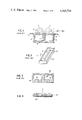
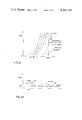
- FIGS. 1 and 2 are cross-sectional and perspective views respectively of a representative prior art planar magnetron sputtering device comprising inner magnet 10 and outer magnet 12 (both of which usually comprise a number of sections) where the magnets are shunted by an iron pole plate 14. Disposed above the magnetic structure is a cathode or target 16 (not shown in FIG. 2). The magnetic lines of force are as shown in FIG. 1 where they exit from and return through cathode 16, a similar technique being employed in U.S. Pat. No. 3,878,085 where the magnetic lines also enter and exit from the cathode surface.
- An electric field is established between (a) a ring-like anode 17, which may be disposed around and spaced from cathode 16, (or the chamber wall may serve this function) and (b) the target whereby electrons are removed from the cathode. Due to the configuration of the lines of magnetic force (the illustration of which is approximate), the removed electrons tend to concentrate in regions A where the lines of force are substantially parallel to the upper surface of target 16. There the electrons ionize gas particles which are then accelerated to the target to dislodge atoms of the target material. The dislodged target material then typically deposits as a coating film on an object to be coated. Assuming the object to be coated is in strip form or is mounted on a strip moving in the direction of the arrow shown in FIG. 2, the object will be uniformly coated, the strip being narrower in width than the length of the sputtering device.
- the ionizing electrons are removed from the target, they travel long paths because they circulate in a closed loop defined between inner magnet 10 and outer magnet 12, the loop being above target 16. Hence, the electrons are effective in ionizing the gas particles. However, since most of the ionizing electrons are concentrated in regions A, the ionized gas particles will mainly erode cathode 16 in regions A'. Such uneven disintegration of the target is undesirable in that the target materials are most often extremely pure and accordingly, very expensive.
- FIG. 3 Another prior art arrangement is shown in cross-section in FIG. 3 where parallel magnets 18 and 20 are employed with pole pieces 22 and 24.
- this configuration is essentially the same as that of FIGS. 1 and 2 in its function and is subject to the same shortcomings.
- FIGS. 1 and 2 are cross-sectional and perspective views respectively of a prior art planar magnetron sputtering device.
- FIG. 3 is a cross-sectional view of another prior art device.
- FIG. 4 is a cross-sectional view of an illustrative magnetic structure in accordance with a presently, non-preferred embodiment of the invention.
- FIG. 5 is a cross-sectional view of an illustrative magnetic structure in accordance with a preferred embodiment of the invention.
- FIG. 6 is a perspective view of an illustrative stacked, flexible magnetic tape for implementing the structure of FIG. 5.
- FIGS. 7 and 8 are plan views of stacked magnetic structures illustrating different corner arrangements thereof.
- FIGS. 9 and 10 are cross-sectional views of illustrative embodiments of further, preferred magnetic structures in accordance with the invention.
- FIG. 11 is an illustrative embodiment of a magnetic structure applicable to small cathodes in accordance with an important aspect of the invention.
- FIG. 12 is a cross-sectional view of a further embodiment of a magnetic structure applicable to small cathodes.
- FIG. 13 is a cross-sectional view of an illustrative embodiment of a further, preferred embodiment of the invention.
- FIG. 14 illustrates (a) a graph showing the flux distribution established by the structure of FIG. 13 and (b) a cross-sectional view of an illustrative embodiment of a further, preferred embodiment of the invention.
- FIG. 15 is a cross-sectional view where the right side portion thereof is an illustrative embodiment of a further, preferred magnetic structure in accordance with the invention and the left side portion thereof is a modified embodiment of the prior art structure illustrated in FIG. 1.
- FIGS. 16 and 17 are cross-sectional views of illustrative embodiments of further, preferred magnetic structures in accordance with the invention where the left and right side portions of each Figure illustrate a particular embodiment of the invention.
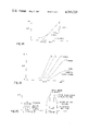
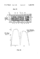
- FIG. 18 illustrates a typical current-voltage characteristic for a magnetically enhanced sputter cathode such as that of the embodiment of FIG. 1.
- FIG. 19 illustrates a family of current-voltage characteristics corresponding to that of FIG. 18 over a range of pressures.
- FIG. 20 illustrates current waveforms associated with the characteristics of FIGS. 18 and 19.
- FIG. 21 illustrates a family of current-voltage characteristics over a range of pressures typical of the magnetic structures of FIGS. 15-17.
- FIG. 22 illustrates various voltage ripple waveforms which occur as the zero impedance portion of the characteristic curves of FIG. 21 is entered.
- FIG. 23 corresponds to the embodiment of FIG. 13 where the left side thereof illustrates field shaping which occurs with a shunt while the right side illustrates the field which results without the shunt.
- FIG. 24 is a cross-sectional view of illustrative embodiments of further, preferred magnetic structures in accordance with the invention where the left and right sides thereof illustrate particular embodiments of the invention.
- FIG. 25 is a cross-sectional view of illustrative embodiments of further, preferred magnetic structures in accordance with the invention where the left and right sides thereof are respective modifications of the left and right sides of FIG. 24.
- FIGS. 26, 27 and 28 are cross-sectional views of illustrative embodiments of further magnetic structures in accordance with the invention where the left and right sides of each Figure illustrate a particular embodiment of the invention.
- FIG. 29 is a graph showing the flux distribution established by the embodiments of FIG. 28.
- FIG. 30 is a cross-sectional view of an illustrative embodiment of the invention suitable for sputter thicker targets used in industrial applications.
- FIG. 31 is a cross-sectional view of an illustrative embodiment of the invention for magnetically shifting plasma across a sputtering surface.
- FIG. 4 there is illustrated a magnetic structure comprising a flat coil solenoid 26 which was tested in an attempt to provide a magnetic flux, which was more uniformly parallel to the surface of the target 16 than that provided by the FIG. 1 structure.
- disintegration of the cathode predominantly occurs where the lines of force are substantially parallel to the cathode surface--that is, at regions A'.
- the area over which the lines of force are substantially parallel is rather minimal and thus uneconomical utilization of the cathode results.
- the FIG. 4 embodiment did generate a desired type of parallel field (the illustration of which is approximate), but the ampere-turns required to generate sufficient magnetic flux (typically over 100 Gauss at 1/2 inch above the coil) was very high. Accordingly, the flat coil solenoid of FIG. 4 is not considered to be a preferred embodiment of the invention at this time.
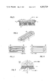
- FIGS. 5 and 6 there is shown an illustrative permanent magnet structure which functionally approximates the FIG. 2 structure, where again the illustrative field is approximate.
- the structure comprises a plurality of flexible magnetic tapes 28 which are concentrically arranged or stacked to form a flat coil as shown in FIG. 6.
- Each ring of the coil comprises a strip of the tape where the ends of each strip abut one another as indicated at 30 for the outer ring.
- the strips are substantially equivalent to a solid magnet where the directions of the flux in each magnet are represented by arrows in FIG. 5 and where the north and south poles of this "solid" magnet are as shown, it being understood that the polarities shown are illustrative and may be reversed, if desired.
- a single strip can be tightly wound to provide a spiral configuration which is also very effective.
- the strips of flexible magnetic tape are oriented ferrite impregnated rubber strips 1/16 inch or 1/8 inch thick.
- ferrite block magnets typically 3/16 inch thick may also be employed to construct a configuration corresponding to that of FIG. 6.
- Sputter cathodes magnetically enhanced by the magnetic structures of the present invention possessed superior performance characteristics compared to those enhanced by the conventional FIG. 1 structure. They support extremely high density plasmas, give better than usual target utilization and provide higher power efficiency than conventionally achieved. They need no pole pieces, can be built at lower cost and promise longer maintenance free life time.
- the rolled and stacked magnet assemblies differ from the conventional magnetic arrays in that they represent a "solid” magnet, as discussed above, rather than several individual magnets pieced together magnetically via the pole pieces or pole plates.
- the performance of the resulting cathodes is closely related to this "solid" form--especially in the corners 34 shown in FIGS. 7 and 8.
- a degree of corner integrity can be readily lost by any gaps between the layers of rubber magnet in the corners. Trying to wind a magnet to best fit a rectangle on the outside and gradually gapping the corners with magnetic material 36 as in FIG. 7 to generate a flattened ellipse in the center will typically result in a much less powerful cathode than will a tight wound flattened ellipse as shown in FIG. 8.
- the flexible magnet materials also make possible many structures that would be most difficult and expensive to achieve in any other way. Even the FIG. 1 type of magnet structure can be given improved properties by interweaved stacking of the corners to provide "corner integrity" using the rubber strips. It may also be possible to achieve the corner integrity by use of permeable metal sheets between layers of blocks or strips in the corner regions.
- the magnets 28 are tipped away from the perpendicular orientation shown in FIG. 5.
- the angle of the magnets with respect to the perpendicular can fall within the 40°-60° range shown in FIG. 9 and preferably this angle should be 50°- 55°.
- Special orientations of the magnets to change the pattern of erosion become quite easy when the flexible magnet system of the present invention is used. As the magnets are tipped toward the center, it is observed that the plasma is affected very little until approximately 40° is reached. At approximately this angle depending upon the geometrics, field strengths, etc., a unique magnetic fused dome structure is formed at the target center line, the illustration of which is approximate.
- FIG. 10 A particularly preferred embodiment of the invention is illustrated in FIG. 10, this embodiment combining the effects provided by the structures of FIGS. 5 and 9. Accordingly with the embodiments of FIG. 10, the strength of the magnetic field above cathode 16 is enhanced by the perpendicular magnets 28' while the erosion of the target center is enhanced by the tipped magnets 28".
- the cathode has a width of 4 inches to 43/4 inches
- the extent of magnets 28" on one side of the cathode might be 1/2 inch to 3/4 inch
- the extent of magnets 28' might be one inch.
- a wedge-like insert 30 of magnetically permeable material is preferably disposed between the perpendicular magnets 28' and the tipped magnets 28".
- clamp rings may be provided to stop erosion at the outer edge of the target. Such a ring is shown at 32 in FIG. 10 where the lines of force are perpendicular to the clamp rings. Further, such clamp rings may be useful in positioning the cathode structure of FIG. 10 within the sputtering device.
- FIG. 11 An attempt was made to construct very small structures corresponding to that of FIG. 1. It was found that at diameters less than about 11/2 inches they would not work in that they would not support a stable magnetically enhanced plasma. At sufficiently high voltage they operated as sputter diodes, with no change in behavior noted in the presence or absence of the magnets. Such a structure is shown in FIG. 11 where the structure corresponds to that shown in FIG. 1 but where the distances between the magnets have been substantially decreased to provide a small sputtering device where the cathode typically has a diameter of one inch or less. Such small devices are useful in many applications.
- a one inch diameter cathode as shown in FIG. 11 can be built using the most powerful ferrite magnets, although it is to be understood that the cathode of FIG. 11 may be elongated rather than circular if so desired. Under most conditions this will not perform in a magnetically enhanced mode.
- An iron filings picture which gives an indication of the positions of the lines of force provides an explanation. The trapping dome is very short, pushed down by strangely shaped lines of force from the outer half of the ring magnet.
- the dome must clear the target surface by at least 3/8 inch for the magnetic structure to be effective. Because of the quadrupole like form above the magnet, the dome is very tightly defined. Changes in target height of a few thousandths of an inch change this from an unenhanced cathode to a violently effective enhanced one.
- the small cathode structure of FIG. 11 has the same general quadrupole-like lines of force as the center effective units of FIGS. 9 and 10 obtained by tipping the magnets. As the small cathode field is reduced, or the cathode dimensions increased, the quadrupole effect becomes undetectable.
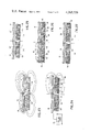
- Other magnetic structures may be employed to effect the quadrupole-like lines of force illustrated in FIGS. 9 and 11. Illustrative of such structures would be that of FIG. 12 which is also particularly applicable to small cathodes of either circular or elongated configuration.
- the magnetic structure includes a pair of C-magnets 40 and 42 in opposing polarity as shown in FIG. 12 where the polarity may be reversed if so desired.
- a pole piece 44 connects the lower arms of the magnets 40 and 42.
- a center magnet 46 is disposed between the magnets 40 and 42 where the polarity of the upper pole thereof is opposite that of the upper arms of the C-magnets and where the magnet 46 may be an extension of pole piece 44, if desired.
- FIG. 1 It is a general teaching of the FIG. 1 structures that the outer pole area should be approximately the same as the inner pole area. In the structures of FIGS. 9, 10 and 11, this teaching has been totally violated. In tipping the magnets in the FIGS. 9 and 10 structures, the lines of force are projected upward from the outer edges, the return path being closed off down the center. In the smaller structure of FIG. 11, the pole areas are loaded ⁇ 10:1 outside to inside. The results are unique.
- Modifying the cross section depth of the magnets can also be used to help shape the parallel Gauss curve and thus the erosion pattern indicated at "x" in FIG. 14. Further, there appears to be many ways the stacked and rolled parallel and tipped magnetic structures of the present invention can be varied to influence target utilization and other performance criteria. Combinations of these effects can also be useful.
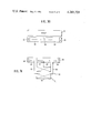
- FIGS. 15, 16 and 17 are cross-sectional views directed to further modifications of the present invention which are stable at extremely low pressures and which have an I-E characteristic that exhibits a zero dynamic impedance in a predetermined band of low pressures.
- FIG. 15 is a modification of the FIG. 1 embodiment of the prior art.
- the portion on the right side of the phantom center line of FIG. 15 corresponds to the new zero dynamic impedance embodiment of the present invention while the left side portion corresponds to an embodiment which provides the normally anticipated infinite dynamic impedance of saturation--that is, positive impedance, as will be discussed in more detail hereinafter.
- the left side of FIG. 1 would be the mirror image of the right side thereof.
- a first plurality of horizontally disposed magnetic strips 50 are disposed on top of a second plurality of horizontally disposed strips 52 where the strips 52 are wider than strips 50.
- a third plurality of horizontally disposed strips 54 are disposed on top of a fourth plurality of strips 56 where the strips 56 are wider than the strips 54.
- the area of target erosion of the FIG. 15 embodiment is increased with respect to that of the FIG. 1 embodiment.
- a solid structure as employed in FIG. 1 may also be used in the embodiment of FIG. 15 or the remaining embodiments where, of course, for the FIG. 15 embodiment, the respective bases of magnets 10 and 12 of FIG. 1 would be widened.
- FIGS. 16 and 17 there are illustrated four further embodiments of the invention, which are capable of achieving the zero dynamic impedance of the present invention.
- FIG. 16 at the left side portion thereof, there is illustrated a first embodiment wherein centrally disposed tipped strips 28" are surrounded by a plurality of horizontally disposed strips 62.
- the right side of FIG. 1 would be the mirror image of the left side thereof.
- this first embodiment corresponds to that of FIG. 10, where the slanted angle of strips 28" would preferably fall within the 40°-60° range discussed hereinbefore with respect to FIG. 9.
- insert 30 may also be employed if desired although it is not needed if good contact is made between an edge of magnets 28" and magnets 62.
- FIG. 16 illustrates a second embodiment capable of producing the zero dynamic impedance of the present invention where the vertically disposed strips 28 correspond to those of FIG. 5 and where they are surrounded by horizontally disposed strips 62.
- the left side of FIG. 16 would be the mirror image of the right side thereof.
- the left side portion of FIG. 17 is a modification of the left side portion of FIG. 16 where, in implementing this embodiment, the right side of FIG. 17 would be the mirror image of the left side thereof.
- the slanted or tipped magnets 28'" have a generally rectangular cross-section where the width of the strips at A and B are more narrow than those at C as shown in FIG. 17.
- a further plurality of vertically disposed strips 64 are disposed between horizontally disposed strips 62 and tipped strips 28'".
- FIG. 17 illustrates a further embodiment where tipped strips 28" are disposed between horizontally disposed strips 62 and vertically disposed strips 66. Again in implementing this embodiment, the left side of FIG. 17 would be the mirror image of the right side thereof.
- a common characteristic of all embodiments is the presence of the outer ring of horizontally disposed strips 62.
- the outer edge of strips 62 is disposed slightly inward of the outer edge of cathode 16 although other relative placements are permissible.
- the strips 62 cause the field on the other side of target 16 to be substantially vertical at the approximate periphery thereof. It is thought that this feature is instrumental in achieving the many advantages associated with not only the embodiments of FIGS. 16 and 17 but also those corresponding to FIG. 15. Increased field strength does not seem to be a contributing factor.
- Magnetically enhanced sputter cathodes such as the embodiment of FIG. 1 typically display a current-voltage characteristic such as that shown in FIG. 18.
- the cathode reaction impedance, Z may be defined as delta E over delta I at any point along the characteristic. This impedance usually assumes a fixed value above a current of a few amperes.
- the initiation voltage, E o may be defined as the zero current intercept of the extrapolated linear portion of the current voltage characteristic.
- the family of characteristics over a range of pressures is shown in FIG. 19 for the conventional magnetron.
- Z p the reaction impedance that is constant at a given pressure changes with pressure, becoming larger at lower pressures.
- the characteristic curves start to break at high power as the pressure is reduced. This is a strong function of magnetic quality, both field strength and corner integrity. With a good magnetic structure, some break will start to occur in the 2 micron argon pressure characteristic.
- These cathodes can sometimes be operated at pressures as low as one micron, but starting becomes difficult, and the discharge will sometimes pop out.
- the lower pressure characteristics lean over or break to show a saturation.
- the current wave form assumes a most unexpected form, as shown in FIG. 20.
- the shape of the current peaks at low power is a function of the three phase power.
- some critical value which is a function of many factors
- the current drops to a very low value, typically a small fraction of an ampere. This is probably the raw electron emission from the target surface.
- the mechanism of this current loss is not known for certain, but sputtering stops during this period. As soon as the voltage drops below this critical value the current starts again, and follows the wave form as before.
- FIG. 21 Characteristics typical of the new cathode magnetic structures of FIGS. 15, 16 and 17 are shown in FIG. 21. Several very interesting differences become obvious. The characteristic is stable to extremely low pressures. A factor of 10 ⁇ lower pressures becomes very practical. This has many meaningful advantages. Sticking is better. Target to substrate distance becomes a less critical factor. Good sticking has been obtained at 18 inches. Also this expanded pressure range makes it possible to measure and control the pressure with an ionization gauge, rather than the conventional thermocouple gauge. This gives better sensitivity, better repeatability, and much faster response. In addition, most pumping systems, such as that diagrammatically indicated at 68 in FIG. 16, can operate under an argon load without interposing a baffle, or valve restriction at this decreased value.
- Z p tends to be constant with the structures of FIGS. 15, 16 and 17, independent of pressure over a wide range of pressure. This suggests that the mechanism of the cathode reaction is not changing over this range.
- a most important characteristic of the new cathode structures of FIGS. 15, 16 and 17 is a very high sputter rate. Rates at all power levels appear to be enhanced by 50 to 100%. In the zero impedance mode the rates are further enhanced to give as much as 400% of the conventional rate at the same power level. In the lower pressure range there appears to be a greater diffusivity of the plasma, resulting in better target utilization.
- iron shunt 38 is employed as a field shaping expedient.
- This magnetic conductor provides a medium through which some of the lines of force from a coil 28 of magnetic source material are shunted, as illustrated in FIG. 23 where the left side of the FIG. approximately illustrates the field shaping which occurs with shunt 38 and the right side the field which results without the shunt.
- this shunting action also bends or deflects some of the remaining lines of force, bringing them into lower, more parallel (to the target surface) position above the target, enhancing and rendering more uniform the plasma layer in the sputtering process.
- shunt 38 removes some of the lines of force from above the target, it is preferable to employ means which provide the bending action but which do not significantly decrease the flux density.
- FIG. 24 There are many magnetic structural configurations that can provide some degree of shaping such as those shown in FIG. 24 at A and B. Magnets perpendicular to the fundamental coils or stacks 28 are shown where in the embodiment illustrated at A a ferrite block magnet 70 is employed and at B a coil or stack 72 of ferrite impregnated rubber strips is employed.
- the block magnet 70 should be sufficiently strong so that it is not demagnetized by stack 28.
- suitable block magnets are 1/4" ⁇ 1" thick ferrite magnets made by Arnold Magnetics, Inc. or Crucible Iron and Steel Co.
- the ferrite impregnated strips of stack 72 may be of the same type employed in stack 28.
- Typical of suitable strips are 1/2" wide ferrite impregnated tapes (such as PL-1.4 H made by Minnesota Mining and Manufacturing Co.).
- the magnet 70 and stack 72 pull down the lines of force issuing from the center of fundamental stack 28 as indicated at FIG. 24B. This action can establish the needed 45° relationship between the lines of force and the target surface, as described hereinbefore, very close to the center of the magnet assembly. Magnets 70 and 72 are more effective than the edges of the individual magnets in fundamental stack 28 due to their projection angle and greater single polarity width.
- the similarity between the embodiments of FIGS. 5 and 24 should be noted, the basic difference, of course, being the presence of magnets 70 and 72.
- the fundamental stack 28 of FIG. 5 establishes a flux therein which is substantially parallel to the lower surface of the target.
- the strength of the field and the parallelism thereof with respect to the target are adequate to achieve uniform target erosion and the other advantages described hereinbefore.
- the size of the cathode is reduced to 41/2 inches or less (which may be the diameter of a circular target or the width from C to D of a generally rectangular or oblong target as indicated in FIG. 5), the field produced by the magnetic structure of FIG.
- FIG. 5 tends to be less parallel to the target surface than is preferred, whereby the erosion is less uniform. Since practical target sizes tend to be 41/2 inches or less, it is thus preferable to modify the FIG. 5 structure in such a way as to effect the desired field shaping (target parallelism). Such modifications are effected by the magnetic field deflectors 38, 70 and 72 of the embodiments of FIGS. 23 and 24, as discussed above. The embodiment illustrated at B in FIG. 24 can also play an important role in shaping about the corners, etc.
- the magnetic deflectors 70, 72, 70' and 72' are intended for maximization of center target utilization.
- outer deflectors 70" and 72" also as shown in FIG. 26. All of the principles related to the inner set 70, 72, 70' and 72' apply also to the outer ones 70" and 72". This thereby extends erosion uniformity both toward the center and toward the outside of the target 16 where further deflectors, in addition to deflectors 70, 72, 70' and 72', may be employed if so desired.
- FIG. 27 It is also possible, as shown in FIG. 27 to use parallel deflectors 74 and 76. Several aspects of the design criteria for these are more critical than for the perpendicular types of FIGS. 24-26. Basically these are like the shunt system of FIG. 13, but more powerful.
- FIGS. 24-27 are particularly powerful although they are somewhat costly for some routine sputter applications.
- the magnets 70, 72, 70', 72', 72", 74 and 76 may be omitted from the embodiments of FIGS. 24-27 in accordance with a further aspect of this invention.
- FIG. 28 where the left side thereof corresponds to the embodiment shown at B in FIG. 24 with an outer perpendicular ring 62 and the right side thereof has an open slot 78 corresponding to magnetic stack 72 where the slot may typically be about 1/2" thick.
- the latter embodiment is less pressure critical for optimization of target utilization than the embodiments of FIGS. 24-27 although there is a slight decrease in power/sputter efficiency.
- slot or gap 78 controls the shape of the top of the parallel field above magnet 28 as does the position of ring 72, this being illustrated in FIG. 29 where the left and right sides thereof respectively correspond to the left and right side embodiments of FIG. 28.
- the optimum location of ring 72 is such that the stacks or rings 28 on opposite sides thereof are approximately equal in length along a line from the center to the periphery of the magnetics while in the embodiment of FIG. 28B, the stack or ring 28 on the inside of slot 78 is optimally about twice as long as the stack or ring 28 on the outside of the slot.
- slot 78 need not completely interrupt stack 28 but may only partially interrupt it in a manner analogous to that of the embodiment of FIG. 25. Further, there may be provided two or more complete or partial slots in a manner analogous to FIG. 26.
- An iron ring or a non-magnetic ring may also be employed in slot(s) 78 in lieu of ring 72 where typically the slot width would be smaller if it contained a non-magnetic ring.
- An iron ring provides some slight advantage over an open slot 78, as indicated in FIG. 29B. Further, the iron ring gives slightly more power to the outer rings of the magnetic structure than does open slot 78.
- the magnetic structures of the present invention satisfy a first condition for obtaining substantially uniform erosion of target 16.
- a second condition for obtaining erosion is that the strength of the magnetic field approximately parallel to and at least 3/8 inch above the target surface should preferably be at least about 80 gauss.
- the two conditions of (a) lines of force having a 45° angle or less with respect to the target and (b) 80 gauss parallel field strength at least 3/8 inch above the target should both be satisfied over as much of the target surface as possible to provide uniformity of target erosion.
- the various embodiments of the present invention satisfy the above requirements with varying degrees of success, the embodiments of FIG. 25 at A and B and of FIG.
- FIG. 25 with an outside vertical stack 62 should also be successful as would be the slotted (whether open or not) embodiments represented by FIG. 28B for many routine sputter applications.
- FIG. 30 shows an illustrative embodiment for sputtering targets of about one inch.
- materials employed in the present invention for magnet construction and especially the ferrite impregnated plastic or rubber materials such as PL-1.4 H made by Minnesota Mining and Manufacturing Co.
- many of the embodiments discussed hereinbefore are typically capable of operating with targets up to 1/2 inch in thickness. In most applications this is sufficient.
- targets of one inch thickness are desired.
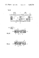
- FIG. 31 shows an illustrative embodiment for increasing the width and uniformity of the erosion pattern on magnetically enhanced sputter cathodes. Because of the high voltages on the cathode structure, it is desirable that there be a minimum of complex operating structure.
- the width and shape of the erosion patterns are a function of magnetic field shapes and strengths as well as the field position relative to the target surface. These parameters may be simultaneously varied without mechanical intervention by combining the embodiments described hereinbefore with a relatively small electromagnet 94 which only provides a changing aspect to the overall field. Electromagnet 94 should be applied with care on alnico magnet systems, in that their strength can be degraded if the field modification is too severe.
- FIG. 31 shows a cross section of a rubber magnetics system 28 and 62 with auxiliary electromagnet 94.
- the magnetic field at the two areas of contact between the fixed magnets 28 and the steel frame 96, 98 are the same.
- the effect on the fixed field should be very minimal.
- electromagnet coil 92 When current is passed through electromagnet coil 92, the two legs 96 and 98 of the frame are forced to different magnetic polarities. This upsets the balance of field and shifts the mechanical position of the center of the magnetic field.
- the center line of the field on the target may receive relatively little erosion. Moving this line permits enhanced erosion to occur across the center of the target, significantly increasing the percentage of utilization of the target.
- Use of AC on the electromagnet oscillates the center automatically from side to side. Correct design of the coil makes it possible to use a fixed voltage transformer to drive the coil.
- the waveshape of the signal should be rectangular or square and the frequency may be about 60 hz although a rather broad range of frequencies may be employed.
- a feature which has been observed with respect to the sputtering device is the large ratio of circulatory Hall effect current with respect to the discharge current passing between the anode and cathode.
- the Hall effect circulatory current results from the closed plasma loop, which may be generated by the magnetic structure of FIG. 6, for example, the plasma loop extending over the sputtering surface in a well known manner as described, for example, in aforementioned U.S. Pat. No. 3,878,085.
- the circulatory current circulates around the plasma loop and is primarily due to the more mobile ionizing electrons.
- the large circulatory current obtainable with the present invention is indicative of the presence of a large number of ionizing electrons to thereby provide high sputtering rates at low pressures.
- the discharge current passing between the anode and cathode is that which conventionally passes through the external circuit connected across these two electrodes. Circulatory currents five to one hundred times greater than the discharge current have been observed. It appears that the strength of the magnetic field generated by the circulatory current approximates that of the field generated by the magnetic structures of the present invention, this being a further indication of the magnitude of this current. It further appears the magnetic field generated by the circulatory current may tend to pinch the closed loop plasma into a thin, intense, ribbon-like sheet although it is not apparent to what extent this pinch effect is achieved. It may be that this effect is instrumental in achieving the high sputter rates at low pressures obtainable with the present invention although there is no intent to be limited to a particular theory of operation.
- the width of uniform target erosion corresponds to the width of the closed loop plasma path discussed above.
- uniformity of the magnetic field around the closed loop path is also desirable.
- the maintenance of a sufficient magnetic field strength over the target to provide electron entrapment is also desirable.
- FIG. 5 is available for larger targets although, of course, the other embodiments of the invention may also be employed.
- the field deflecting means described hereinbefore with respect to FIGS. 13 and 23-28 are preferred.
- these embodiments include at least one magnet (stack 28, for example) which establishes the generally parallel field to the sputtering surface.
- This field may be rendered more parallel with respect to the sputtering surface by additional magnets in magnetic circuit with (a) the first magnet 28, such as additional magnets 70, 72, 70', 72', etc., where magnets 70 and 72 completely interrupt the flux through stack 28 while magnets 70' and 72' only partially interrupt this flux and (b) the lines of force over the target surface.
- slot 78 which may be open or which may contain an appropriate insert, may also act as means for effecting the requisite field deflection to render the lines of force more parallel to the target surface.
- Uniformity of the magnetic field above the sputtering surface around the closed loop at least in the central portion of the field may be obtained by the use of the flexible magnetic structures illustrated in FIGS. 5 and 8.
- Illustrative of such flexible magnetic structures are the magnetic tape embodiments described hereinbefore.
- the desired strength of the magnetic field (typically a parallel field strength of at least 80 gauss at least 3/8 inch above the sputtering surface) is preferably obtained with the ferrite magnets described hereinbefore where the rubber or plastic tapes impregnated with ferrite particles are advantageous.
- the presence of these particles, which are capable of producing a very strong magnetic field, in a low permeability binder such as rubber or plastic, is apparently advantageous in generating fields having the requisite strength, although it is to be understood that other ferrite magnets may be employed as may be appropriate ferromagnetic magnets such as alnico magnets.
- magnet 62 of FIGS. 15-17, 26-28, 30 and 31 may be employed for achieving this feature of the invention.
- the south pole, for example, of magnet 62 is adjacent that of magnet 28.
- the close justaposition of these like poles is a further factor in promoting parallelism of the lines of force to the very edge of the plasma path, at which point the lines of force are directed substantially perpendicularly through the target edge to thereby limit further erosion thereof.
- the lines of force should be rectangular in configuration (as opposed to curved) over the sputtering surface and the field shaping techniques of the present invention have been so utilized as to approach this ideal with varying degrees of success while at the same time providing sufficient field strength over the target.
- both of these members are magnets as opposed to members made of mon-magnetized, magnetically permeable material such as iron pole pieces frequently used in magnetic structures to direct lines of force. Such pole pieces and the like do not effect the requisite field shaping and/or generate the requisite field strength as is obtained by the present invention.
- the direction of the flux in fundamental magnet 28 is preferably inclined at an angle with respect to the flux in magnets 28", 62, 70, 71', etc.
- the desired field shaping depends to a certain extent on the respective inclinations of the fluxes in the different magnets as well as their respective strengths.
- the flux in magnet 28 is parallel to the target surface and those in the field shaping magnets is at an angle of 90° with respect to that in magnet 28, although, as in FIG. 27, the flux in the field shaping magnet can be opposite to that in magnet 28.
- the strength of the field shaping magnets should be such that they are not de-magnetized by fundamental magnet 28 or vice versa.
- various combinations of magnets, slots, iron rings, etc. may be employed if so desired.
- electromagnets may also be employed as indicated, for example, in FIG. 4.
- the magnetic structures of the present invention may be employed with planar cathodes which are circular or oblong.
- Oblong cathodes may be rectangular, elliptical or oval.
- the planar cathode may be annular.
- the planar cathode may include non-linear portions such as the concave portions shown in the cathodes of FIGS. 5 and 7 of aforementioned U.S. Pat. No. 3,878,085.
- cylindrical, conical, closed belt, etc. cathodes may also be employed. Also, as the cathode is sputtered, there will be a tendency for it to become concave.
- the cathode may still be considered planar, cylindrical or whatever its original shape was. Further, contoured surfaces may be imparted to the cathode so that it is thicker in areas of greatest expected erosion whereby the target will sputter relatively uniformly. Again, such a cathode is to be considered planar, cylindrical, etc. depending upon its general configuration prior to sputtering thereof.
- the target material to be sputtered may or may not be the cathode of the device. If not, it may be clamped to the cathode by a clamp similar to clamp 32 of FIG. 10. Clamp 32 may also be employed to secure the cathode to the magnetic structure when the cathode and target are one and the same. When the target is distinct from the cathode, it may or may not be co-extensive therewith. If the target is smaller than the cathode, the magnetic lines of force may return to the magnetic structure through the cathode rather than the target. As long as the lines of force are substantially perpendicular to the cathode where they pass therethrough, sputtering of the cathode is minimized.
- the lines of force can be returned through clamp 32, the lines being substantially perpendicular to the surface thereof to thereby minimize erosion thereof.
- clamp 32 (whether it is used to clamp the target to the cathode or to position the cathode within the magnetic structure) is in electrical contact with and connected to the cathode although it is not a part of the cathode structure.
- member 32 may be slightly spaced from the cathode so that the lines of force return perpendicularly therethrough and yet little, if any, plasma escapes betweem member 32 and the cathode since the spacing is so small that a plasma cannot be formed therebetween.
- the member 32 can thus provide a path for return of the magnetic lines of force and further prevent lines of force from returning to the anode which would permit electrons to escape from the plasma. Further, spaced member 32 may be biased somewhat negatively with respect to the cathode to effect repulsion of electrons therefrom and maintain electron entrapment.
- anode it is usually so-called because sputtering systems are typically self-rectifying when an AC potential is applied.
- the term anode is employed in the following claims, it is to be understood that it may be any other equivalent electrode in the system.
- the anode can be the container wall of the sputtering device.
- DC, low frequency AC (60 Hz, for example) or industrial radio frequencies, such as 13.56 MHz or 27.12 MHz, may be applied across the anode and cathode.
- the anode is almost always the container wall when these high frequencies are employed although it is quite often employed as the anode when DC is employed.
- the gas employed in the system it may be either active or inert depending upon the type of sputtered layer desired.
Abstract
Description
Claims (78)
Priority Applications (5)
| Application Number | Priority Date | Filing Date | Title |
|---|---|---|---|
| US06/019,284 US4265729A (en) | 1978-09-27 | 1979-03-09 | Magnetically enhanced sputtering device |
| GB7912472A GB2028377B (en) | 1978-08-21 | 1979-04-09 | Magnetically-enhanced sputtering device |
| CA000325126A CA1141704A (en) | 1978-08-21 | 1979-04-09 | Magnetically enhanced sputtering device |
| FR7909442A FR2434479A1 (en) | 1978-08-21 | 1979-04-13 | DEVICE FOR CATHODE SPRAYING OR METALLIZATION WITH IMPROVED MAGNETIC EFFECT |
| DE19792920780 DE2920780C2 (en) | 1978-08-21 | 1979-05-22 | Magnetic amplification atomizer |
Applications Claiming Priority (2)
| Application Number | Priority Date | Filing Date | Title |
|---|---|---|---|
| US05/946,370 US4180450A (en) | 1978-08-21 | 1978-09-27 | Planar magnetron sputtering device |
| US06/019,284 US4265729A (en) | 1978-09-27 | 1979-03-09 | Magnetically enhanced sputtering device |
Related Parent Applications (1)
| Application Number | Title | Priority Date | Filing Date |
|---|---|---|---|
| US05/946,370 Continuation-In-Part US4180450A (en) | 1978-08-21 | 1978-09-27 | Planar magnetron sputtering device |
Related Child Applications (1)
| Application Number | Title | Priority Date | Filing Date |
|---|---|---|---|
| US06/047,248 Continuation-In-Part US4239611A (en) | 1979-06-11 | 1979-06-11 | Magnetron sputtering devices |
Publications (1)
| Publication Number | Publication Date |
|---|---|
| US4265729A true US4265729A (en) | 1981-05-05 |
Family
ID=26692077
Family Applications (1)
| Application Number | Title | Priority Date | Filing Date |
|---|---|---|---|
| US06/019,284 Expired - Lifetime US4265729A (en) | 1978-08-21 | 1979-03-09 | Magnetically enhanced sputtering device |
Country Status (1)
| Country | Link |
|---|---|
| US (1) | US4265729A (en) |
Cited By (47)
| Publication number | Priority date | Publication date | Assignee | Title |
|---|---|---|---|---|
| US4361472A (en) * | 1980-09-15 | 1982-11-30 | Vac-Tec Systems, Inc. | Sputtering method and apparatus utilizing improved ion source |
| EP0070574A1 (en) * | 1981-07-22 | 1983-01-26 | Hitachi, Ltd. | Film forming method |
| US4391697A (en) * | 1982-08-16 | 1983-07-05 | Vac-Tec Systems, Inc. | High rate magnetron sputtering of high permeability materials |
| US4401539A (en) * | 1981-01-30 | 1983-08-30 | Hitachi, Ltd. | Sputtering cathode structure for sputtering apparatuses, method of controlling magnetic flux generated by said sputtering cathode structure, and method of forming films by use of said sputtering cathode structure |
| US4404077A (en) * | 1981-04-07 | 1983-09-13 | Fournier Paul R | Integrated sputtering apparatus and method |
| US4412907A (en) * | 1982-07-23 | 1983-11-01 | Nihon Shinku Gijutsu Kabushiki Kaisha | Ferromagnetic high speed sputtering apparatus |
| US4431505A (en) * | 1982-08-16 | 1984-02-14 | Vac-Tec Systems, Inc. | High rate magnetron sputtering of high permeability materials |
| US4441974A (en) * | 1982-04-30 | 1984-04-10 | Tokyo Shibaura Denki Kabushiki Kaisha | Magnetron sputtering apparatus |
| US4448653A (en) * | 1980-10-14 | 1984-05-15 | Balzers Aktiengesellschaft | Cathode arrangement for sputtering material from a target in a cathode sputtering unit |
| US4457825A (en) * | 1980-05-16 | 1984-07-03 | Varian Associates, Inc. | Sputter target for use in a sputter coating source |
| US4486289A (en) * | 1982-02-05 | 1984-12-04 | University Of British Columbia, Canada | Planar magnetron sputtering device |
| US4486287A (en) * | 1984-02-06 | 1984-12-04 | Fournier Paul R | Cross-field diode sputtering target assembly |
| FR2549495A1 (en) * | 1983-07-19 | 1985-01-25 | Varian Associates | MAGNETRON SPRAY COATING SOURCE FOR MAGNETIC AND NON-MAGNETIC TARGETS |
| US4500409A (en) * | 1983-07-19 | 1985-02-19 | Varian Associates, Inc. | Magnetron sputter coating source for both magnetic and non magnetic target materials |
| US4500408A (en) * | 1983-07-19 | 1985-02-19 | Varian Associates, Inc. | Apparatus for and method of controlling sputter coating |
| EP0148470A2 (en) * | 1983-12-21 | 1985-07-17 | Hitachi, Ltd. | Planar magnetron sputtering with modified field configuration |
| US4552639A (en) * | 1984-07-20 | 1985-11-12 | Varian Associates, Inc. | Magnetron sputter etching system |
| US4569746A (en) * | 1984-05-17 | 1986-02-11 | Varian Associates, Inc. | Magnetron sputter device using the same pole piece for coupling separate confining magnetic fields to separate targets subject to separate discharges |
| US4595482A (en) * | 1984-05-17 | 1986-06-17 | Varian Associates, Inc. | Apparatus for and the method of controlling magnetron sputter device having separate confining magnetic fields to separate targets subject to separate discharges |
| US4597847A (en) * | 1984-10-09 | 1986-07-01 | Iodep, Inc. | Non-magnetic sputtering target |
| US4604180A (en) * | 1984-01-20 | 1986-08-05 | Anelva Corporation | Target assembly capable of attaining a high step coverage ratio in a magnetron-type sputtering device |
| US4606806A (en) * | 1984-05-17 | 1986-08-19 | Varian Associates, Inc. | Magnetron sputter device having planar and curved targets |
| US4622122A (en) * | 1986-02-24 | 1986-11-11 | Oerlikon Buhrle U.S.A. Inc. | Planar magnetron cathode target assembly |
| US4632719A (en) * | 1985-09-18 | 1986-12-30 | Varian Associates, Inc. | Semiconductor etching apparatus with magnetic array and vertical shield |
| US4668365A (en) * | 1984-10-25 | 1987-05-26 | Applied Materials, Inc. | Apparatus and method for magnetron-enhanced plasma-assisted chemical vapor deposition |
| US4673480A (en) * | 1980-05-16 | 1987-06-16 | Varian Associates, Inc. | Magnetically enhanced sputter source |
| US4724058A (en) * | 1984-08-13 | 1988-02-09 | Vac-Tec Systems, Inc. | Method and apparatus for arc evaporating large area targets |
| US4812217A (en) * | 1987-04-27 | 1989-03-14 | American Telephone And Telegraph Company, At&T Bell Laboratories | Method and apparatus for feeding and coating articles in a controlled atmosphere |
| US4865708A (en) * | 1988-11-14 | 1989-09-12 | Vac-Tec Systems, Inc. | Magnetron sputtering cathode |
| US4892633A (en) * | 1988-11-14 | 1990-01-09 | Vac-Tec Systems, Inc. | Magnetron sputtering cathode |
| EP0381437A2 (en) * | 1989-01-30 | 1990-08-08 | Mitsubishi Chemical Corporation | Magnetron sputtering apparatus |
| US4964968A (en) * | 1988-04-30 | 1990-10-23 | Mitsubishi Kasei Corp. | Magnetron sputtering apparatus |
| GB2241710A (en) * | 1990-02-16 | 1991-09-11 | Ion Tech Ltd | Magnetron sputtering of magnetic materials in which magnets are unbalanced |
| US5130005A (en) * | 1990-10-31 | 1992-07-14 | Materials Research Corporation | Magnetron sputter coating method and apparatus with rotating magnet cathode |
| US5215639A (en) * | 1984-10-09 | 1993-06-01 | Genus, Inc. | Composite sputtering target structures and process for producing such structures |
| US5262028A (en) * | 1992-06-01 | 1993-11-16 | Sierra Applied Sciences, Inc. | Planar magnetron sputtering magnet assembly |
| US5458754A (en) | 1991-04-22 | 1995-10-17 | Multi-Arc Scientific Coatings | Plasma enhancement apparatus and method for physical vapor deposition |
| US6077407A (en) * | 1998-05-04 | 2000-06-20 | Leybold Systems Gmbh | Sputtering cathode based on the magnetron principle |
| US6207028B1 (en) * | 1998-08-10 | 2001-03-27 | Leybold Systems Gmbh | Sputtering device with a cathode with permanent magnet system |
| EP1193729A2 (en) * | 2000-09-28 | 2002-04-03 | The Boc Group, Inc. | Method and apparatus for magnetron sputtering |
| US6377149B1 (en) * | 1998-05-22 | 2002-04-23 | Shin-Etsu Chemical Co., Ltd. | Magnetic field generator for magnetron plasma generation |
| WO2002099841A1 (en) * | 2001-06-06 | 2002-12-12 | Applied Materials, Inc. | High performance magnetron for dc sputtering systems |
| US20050082166A1 (en) * | 2003-10-16 | 2005-04-21 | Applied Vacuum Coating Technologies Co., Ltd. | Cathode structure for vacuum sputtering machine |
| US20080110749A1 (en) * | 2006-05-16 | 2008-05-15 | Siegfried Krassnitzer | Arc source and magnet configuration |
| US20110305912A1 (en) * | 2006-07-13 | 2011-12-15 | Dennis Teer | Coating apparatus and method |
| US8685214B1 (en) | 2011-09-30 | 2014-04-01 | WD Media, LLC | Magnetic shunting pads for optimizing target erosion in sputtering processes |
| US20140333399A1 (en) * | 2013-05-08 | 2014-11-13 | Franklin Limberg | Pseudo mechanical energy generator |
Citations (10)
| Publication number | Priority date | Publication date | Assignee | Title |
|---|---|---|---|---|
| US3956093A (en) * | 1974-12-16 | 1976-05-11 | Airco, Inc. | Planar magnetron sputtering method and apparatus |
| DE2707144A1 (en) * | 1976-02-19 | 1977-08-25 | Sloan Technology Corp | Cathode sputtering device with magnetic equipment - which can be displaced to move the area of sputtering over an extended surface by relative movement |
| US4046660A (en) * | 1975-12-29 | 1977-09-06 | Bell Telephone Laboratories, Incorporated | Sputter coating with charged particle flux control |
| US4060470A (en) * | 1974-12-06 | 1977-11-29 | Clarke Peter J | Sputtering apparatus and method |
| US4100055A (en) * | 1977-06-10 | 1978-07-11 | Varian Associates, Inc. | Target profile for sputtering apparatus |
| US4116806A (en) * | 1977-12-08 | 1978-09-26 | Battelle Development Corporation | Two-sided planar magnetron sputtering apparatus |
| GB2002036A (en) * | 1977-08-06 | 1979-02-14 | Leybold Heraeus Gmbh & Co Kg | Cathode sputtering apparatus |
| US4155825A (en) * | 1977-05-02 | 1979-05-22 | Fournier Paul R | Integrated sputtering apparatus and method |
| US4162954A (en) * | 1978-08-21 | 1979-07-31 | Vac-Tec Systems, Inc. | Planar magnetron sputtering device |
| US4194962A (en) * | 1978-12-20 | 1980-03-25 | Advanced Coating Technology, Inc. | Cathode for sputtering |
-
1979
- 1979-03-09 US US06/019,284 patent/US4265729A/en not_active Expired - Lifetime
Patent Citations (10)
| Publication number | Priority date | Publication date | Assignee | Title |
|---|---|---|---|---|
| US4060470A (en) * | 1974-12-06 | 1977-11-29 | Clarke Peter J | Sputtering apparatus and method |
| US3956093A (en) * | 1974-12-16 | 1976-05-11 | Airco, Inc. | Planar magnetron sputtering method and apparatus |
| US4046660A (en) * | 1975-12-29 | 1977-09-06 | Bell Telephone Laboratories, Incorporated | Sputter coating with charged particle flux control |
| DE2707144A1 (en) * | 1976-02-19 | 1977-08-25 | Sloan Technology Corp | Cathode sputtering device with magnetic equipment - which can be displaced to move the area of sputtering over an extended surface by relative movement |
| US4155825A (en) * | 1977-05-02 | 1979-05-22 | Fournier Paul R | Integrated sputtering apparatus and method |
| US4100055A (en) * | 1977-06-10 | 1978-07-11 | Varian Associates, Inc. | Target profile for sputtering apparatus |
| GB2002036A (en) * | 1977-08-06 | 1979-02-14 | Leybold Heraeus Gmbh & Co Kg | Cathode sputtering apparatus |
| US4116806A (en) * | 1977-12-08 | 1978-09-26 | Battelle Development Corporation | Two-sided planar magnetron sputtering apparatus |
| US4162954A (en) * | 1978-08-21 | 1979-07-31 | Vac-Tec Systems, Inc. | Planar magnetron sputtering device |
| US4194962A (en) * | 1978-12-20 | 1980-03-25 | Advanced Coating Technology, Inc. | Cathode for sputtering |
Cited By (58)
| Publication number | Priority date | Publication date | Assignee | Title |
|---|---|---|---|---|
| US4673480A (en) * | 1980-05-16 | 1987-06-16 | Varian Associates, Inc. | Magnetically enhanced sputter source |
| US4457825A (en) * | 1980-05-16 | 1984-07-03 | Varian Associates, Inc. | Sputter target for use in a sputter coating source |
| US4361472A (en) * | 1980-09-15 | 1982-11-30 | Vac-Tec Systems, Inc. | Sputtering method and apparatus utilizing improved ion source |
| US4448653A (en) * | 1980-10-14 | 1984-05-15 | Balzers Aktiengesellschaft | Cathode arrangement for sputtering material from a target in a cathode sputtering unit |
| US4401539A (en) * | 1981-01-30 | 1983-08-30 | Hitachi, Ltd. | Sputtering cathode structure for sputtering apparatuses, method of controlling magnetic flux generated by said sputtering cathode structure, and method of forming films by use of said sputtering cathode structure |
| US4404077A (en) * | 1981-04-07 | 1983-09-13 | Fournier Paul R | Integrated sputtering apparatus and method |
| US4444635A (en) * | 1981-07-22 | 1984-04-24 | Hitachi, Ltd. | Film forming method |
| EP0070574A1 (en) * | 1981-07-22 | 1983-01-26 | Hitachi, Ltd. | Film forming method |
| US4486289A (en) * | 1982-02-05 | 1984-12-04 | University Of British Columbia, Canada | Planar magnetron sputtering device |
| US4441974A (en) * | 1982-04-30 | 1984-04-10 | Tokyo Shibaura Denki Kabushiki Kaisha | Magnetron sputtering apparatus |
| US4412907A (en) * | 1982-07-23 | 1983-11-01 | Nihon Shinku Gijutsu Kabushiki Kaisha | Ferromagnetic high speed sputtering apparatus |
| US4391697A (en) * | 1982-08-16 | 1983-07-05 | Vac-Tec Systems, Inc. | High rate magnetron sputtering of high permeability materials |
| US4431505A (en) * | 1982-08-16 | 1984-02-14 | Vac-Tec Systems, Inc. | High rate magnetron sputtering of high permeability materials |
| FR2549495A1 (en) * | 1983-07-19 | 1985-01-25 | Varian Associates | MAGNETRON SPRAY COATING SOURCE FOR MAGNETIC AND NON-MAGNETIC TARGETS |
| US4500409A (en) * | 1983-07-19 | 1985-02-19 | Varian Associates, Inc. | Magnetron sputter coating source for both magnetic and non magnetic target materials |
| US4500408A (en) * | 1983-07-19 | 1985-02-19 | Varian Associates, Inc. | Apparatus for and method of controlling sputter coating |
| EP0148470A2 (en) * | 1983-12-21 | 1985-07-17 | Hitachi, Ltd. | Planar magnetron sputtering with modified field configuration |
| EP0148470B1 (en) * | 1983-12-21 | 1989-08-02 | Hitachi, Ltd. | Planar magnetron sputtering with modified field configuration |
| US4604180A (en) * | 1984-01-20 | 1986-08-05 | Anelva Corporation | Target assembly capable of attaining a high step coverage ratio in a magnetron-type sputtering device |
| US4486287A (en) * | 1984-02-06 | 1984-12-04 | Fournier Paul R | Cross-field diode sputtering target assembly |
| US4595482A (en) * | 1984-05-17 | 1986-06-17 | Varian Associates, Inc. | Apparatus for and the method of controlling magnetron sputter device having separate confining magnetic fields to separate targets subject to separate discharges |
| US4569746A (en) * | 1984-05-17 | 1986-02-11 | Varian Associates, Inc. | Magnetron sputter device using the same pole piece for coupling separate confining magnetic fields to separate targets subject to separate discharges |
| US4606806A (en) * | 1984-05-17 | 1986-08-19 | Varian Associates, Inc. | Magnetron sputter device having planar and curved targets |
| US4552639A (en) * | 1984-07-20 | 1985-11-12 | Varian Associates, Inc. | Magnetron sputter etching system |
| US4724058A (en) * | 1984-08-13 | 1988-02-09 | Vac-Tec Systems, Inc. | Method and apparatus for arc evaporating large area targets |
| US5215639A (en) * | 1984-10-09 | 1993-06-01 | Genus, Inc. | Composite sputtering target structures and process for producing such structures |
| US4597847A (en) * | 1984-10-09 | 1986-07-01 | Iodep, Inc. | Non-magnetic sputtering target |
| US4668365A (en) * | 1984-10-25 | 1987-05-26 | Applied Materials, Inc. | Apparatus and method for magnetron-enhanced plasma-assisted chemical vapor deposition |
| US4632719A (en) * | 1985-09-18 | 1986-12-30 | Varian Associates, Inc. | Semiconductor etching apparatus with magnetic array and vertical shield |
| US4622122A (en) * | 1986-02-24 | 1986-11-11 | Oerlikon Buhrle U.S.A. Inc. | Planar magnetron cathode target assembly |
| US4812217A (en) * | 1987-04-27 | 1989-03-14 | American Telephone And Telegraph Company, At&T Bell Laboratories | Method and apparatus for feeding and coating articles in a controlled atmosphere |
| US4964968A (en) * | 1988-04-30 | 1990-10-23 | Mitsubishi Kasei Corp. | Magnetron sputtering apparatus |
| US4865708A (en) * | 1988-11-14 | 1989-09-12 | Vac-Tec Systems, Inc. | Magnetron sputtering cathode |
| US4892633A (en) * | 1988-11-14 | 1990-01-09 | Vac-Tec Systems, Inc. | Magnetron sputtering cathode |
| WO1990005793A1 (en) * | 1988-11-14 | 1990-05-31 | Vac-Tec Systems, Inc. | Improved magnetron sputtering cathode |
| EP0645798A1 (en) * | 1989-01-30 | 1995-03-29 | Mitsubishi Kasei Corporation | Magnetron sputtering apparatus |
| EP0381437A3 (en) * | 1989-01-30 | 1991-03-27 | Mitsubishi Chemical Corporation | Magnetron sputtering apparatus |
| EP0381437A2 (en) * | 1989-01-30 | 1990-08-08 | Mitsubishi Chemical Corporation | Magnetron sputtering apparatus |
| GB2241710A (en) * | 1990-02-16 | 1991-09-11 | Ion Tech Ltd | Magnetron sputtering of magnetic materials in which magnets are unbalanced |
| US5130005A (en) * | 1990-10-31 | 1992-07-14 | Materials Research Corporation | Magnetron sputter coating method and apparatus with rotating magnet cathode |
| US5458754A (en) | 1991-04-22 | 1995-10-17 | Multi-Arc Scientific Coatings | Plasma enhancement apparatus and method for physical vapor deposition |
| US6139964A (en) | 1991-04-22 | 2000-10-31 | Multi-Arc Inc. | Plasma enhancement apparatus and method for physical vapor deposition |
| US5262028A (en) * | 1992-06-01 | 1993-11-16 | Sierra Applied Sciences, Inc. | Planar magnetron sputtering magnet assembly |
| WO1993024674A1 (en) * | 1992-06-01 | 1993-12-09 | Barry Manley | Improved planar magnetron sputtering magnet assembly |
| US6077407A (en) * | 1998-05-04 | 2000-06-20 | Leybold Systems Gmbh | Sputtering cathode based on the magnetron principle |
| US6377149B1 (en) * | 1998-05-22 | 2002-04-23 | Shin-Etsu Chemical Co., Ltd. | Magnetic field generator for magnetron plasma generation |
| US6207028B1 (en) * | 1998-08-10 | 2001-03-27 | Leybold Systems Gmbh | Sputtering device with a cathode with permanent magnet system |
| EP1193729A2 (en) * | 2000-09-28 | 2002-04-03 | The Boc Group, Inc. | Method and apparatus for magnetron sputtering |
| JP2002161364A (en) * | 2000-09-28 | 2002-06-04 | Boc Group Inc:The | High target utilization magnet array and related methods |
| EP1193729A3 (en) * | 2000-09-28 | 2006-01-25 | The Boc Group, Inc. | Method and apparatus for magnetron sputtering |
| WO2002099841A1 (en) * | 2001-06-06 | 2002-12-12 | Applied Materials, Inc. | High performance magnetron for dc sputtering systems |
| US20050082166A1 (en) * | 2003-10-16 | 2005-04-21 | Applied Vacuum Coating Technologies Co., Ltd. | Cathode structure for vacuum sputtering machine |
| US20080110749A1 (en) * | 2006-05-16 | 2008-05-15 | Siegfried Krassnitzer | Arc source and magnet configuration |
| US9165749B2 (en) | 2006-05-16 | 2015-10-20 | Oerlikon Trading Ag, Truebbach | Arc source and magnet configuration |
| US20110305912A1 (en) * | 2006-07-13 | 2011-12-15 | Dennis Teer | Coating apparatus and method |
| US8440301B2 (en) * | 2006-07-13 | 2013-05-14 | Teer Coatings Limited | Coating apparatus and method |
| US8685214B1 (en) | 2011-09-30 | 2014-04-01 | WD Media, LLC | Magnetic shunting pads for optimizing target erosion in sputtering processes |
| US20140333399A1 (en) * | 2013-05-08 | 2014-11-13 | Franklin Limberg | Pseudo mechanical energy generator |
Similar Documents
| Publication | Publication Date | Title |
|---|---|---|
| US4265729A (en) | Magnetically enhanced sputtering device | |
| US4180450A (en) | Planar magnetron sputtering device | |
| US4162954A (en) | Planar magnetron sputtering device | |
| US4239611A (en) | Magnetron sputtering devices | |
| US7259378B2 (en) | Closed drift ion source | |
| US4312731A (en) | Magnetically enhanced sputtering device and method | |
| US6919672B2 (en) | Closed drift ion source | |
| GB2028377A (en) | Magnetically-Enhanced Sputtering Device | |
| GB2051877A (en) | Magnetically Enhanced Sputtering Device and Method | |
| JP4817592B2 (en) | Magnetron plasma magnetic field generator, plasma etching apparatus and method using the magnetic field generator | |
| US5106470A (en) | Method and device for controlling an electromagnet for a magnetron sputtering source | |
| EP0381437A2 (en) | Magnetron sputtering apparatus | |
| JPH0525625A (en) | Magnetron sputtering cathode | |
| JPH07157874A (en) | Magnetron sputtering device | |
| JP2604442B2 (en) | Magnetron sputtering equipment | |
| JPH028366A (en) | Magnetron sputtering device | |
| JP5306425B6 (en) | Magnetic field generator for magnetron plasma | |
| JPH04358064A (en) | Magnetron sputtering cathode | |
| JPH0641737A (en) | Magnetron sputtering device | |
| JP3211915B2 (en) | Magnetron sputtering cathode | |
| JPH0351788B2 (en) | ||
| JPH01104771A (en) | Plate magnetron sputtering device | |
| JPH0445267A (en) | Sputtering system | |
| JPH04202770A (en) | Magnetron sputtering system | |
| JPH06136528A (en) | Magnetron sputtering device |
Legal Events
| Date | Code | Title | Description |
|---|---|---|---|
| STCF | Information on status: patent grant |
Free format text: PATENTED CASE |
|
| AS | Assignment |
Owner name: AMDURA CORPORATION Free format text: SECURITY INTEREST;ASSIGNOR:VAC-TEC SYSTEMS, INC.;REEL/FRAME:005947/0097 Effective date: 19911018 Owner name: CONNOLLY, TOM H., TRUSTEE Free format text: SECURITY INTEREST;ASSIGNOR:AMDURA CORPORATION A CORP. OF DE;REEL/FRAME:005947/0702 Effective date: 19911023 |
|
| AS | Assignment |
Owner name: AMDURA LIQUIDATING TRUST, COLORADO Free format text: ASSIGNMENT OF ASSIGNORS INTEREST.;ASSIGNOR:VAC-TEC SYSTEMS, INC.;REEL/FRAME:006318/0268 Effective date: 19921101 |
|
| AS | Assignment |
Owner name: HAUZER INDUSTRIES BV, NETHERLANDS Free format text: ASSIGNMENT OF ASSIGNORS INTEREST.;ASSIGNOR:AMDURA LIQUIDATING TRUST;REEL/FRAME:006306/0422 Effective date: 19921112 |