US4266334A - Manufacture of thinned substrate imagers - Google Patents
Manufacture of thinned substrate imagers Download PDFInfo
- Publication number
- US4266334A US4266334A US06/098,699 US9869979A US4266334A US 4266334 A US4266334 A US 4266334A US 9869979 A US9869979 A US 9869979A US 4266334 A US4266334 A US 4266334A
- Authority
- US
- United States
- Prior art keywords
- wafer
- thinned
- back surface
- thinning
- glass
- Prior art date
- Legal status (The legal status is an assumption and is not a legal conclusion. Google has not performed a legal analysis and makes no representation as to the accuracy of the status listed.)
- Expired - Lifetime
Links
- 239000000758 substrate Substances 0.000 title claims abstract description 30
- 238000004519 manufacturing process Methods 0.000 title claims description 8
- 239000011521 glass Substances 0.000 claims abstract description 34
- 238000000576 coating method Methods 0.000 claims abstract description 11
- 230000002093 peripheral effect Effects 0.000 claims abstract description 10
- 239000011248 coating agent Substances 0.000 claims abstract description 8
- 238000005520 cutting process Methods 0.000 claims abstract description 3
- 238000000034 method Methods 0.000 claims description 26
- XUIMIQQOPSSXEZ-UHFFFAOYSA-N Silicon Chemical compound [Si] XUIMIQQOPSSXEZ-UHFFFAOYSA-N 0.000 claims description 11
- 229910052710 silicon Inorganic materials 0.000 claims description 11
- 239000010703 silicon Substances 0.000 claims description 11
- 239000002253 acid Substances 0.000 claims description 9
- 239000003292 glue Substances 0.000 claims description 5
- 230000000873 masking effect Effects 0.000 claims description 5
- 239000000463 material Substances 0.000 claims description 5
- 238000003825 pressing Methods 0.000 claims description 2
- 238000004026 adhesive bonding Methods 0.000 claims 4
- 239000000126 substance Substances 0.000 abstract description 6
- 239000004065 semiconductor Substances 0.000 abstract description 2
- 239000000853 adhesive Substances 0.000 description 13
- 230000001070 adhesive effect Effects 0.000 description 13
- 239000010410 layer Substances 0.000 description 5
- 238000012546 transfer Methods 0.000 description 5
- VYPSYNLAJGMNEJ-UHFFFAOYSA-N Silicium dioxide Chemical compound O=[Si]=O VYPSYNLAJGMNEJ-UHFFFAOYSA-N 0.000 description 4
- 230000003287 optical effect Effects 0.000 description 4
- 238000012360 testing method Methods 0.000 description 4
- QTBSBXVTEAMEQO-UHFFFAOYSA-N Acetic acid Chemical compound CC(O)=O QTBSBXVTEAMEQO-UHFFFAOYSA-N 0.000 description 3
- 239000000203 mixture Substances 0.000 description 3
- 230000035945 sensitivity Effects 0.000 description 3
- 239000004593 Epoxy Substances 0.000 description 2
- KRHYYFGTRYWZRS-UHFFFAOYSA-N Fluorane Chemical compound F KRHYYFGTRYWZRS-UHFFFAOYSA-N 0.000 description 2
- 230000002411 adverse Effects 0.000 description 2
- 238000013459 approach Methods 0.000 description 2
- 238000010276 construction Methods 0.000 description 2
- 230000000694 effects Effects 0.000 description 2
- 238000005530 etching Methods 0.000 description 2
- 238000005286 illumination Methods 0.000 description 2
- 239000012535 impurity Substances 0.000 description 2
- 230000010354 integration Effects 0.000 description 2
- 239000007788 liquid Substances 0.000 description 2
- 229910021420 polycrystalline silicon Inorganic materials 0.000 description 2
- 229920005591 polysilicon Polymers 0.000 description 2
- 238000012545 processing Methods 0.000 description 2
- 239000000523 sample Substances 0.000 description 2
- 239000000377 silicon dioxide Substances 0.000 description 2
- LIVNPJMFVYWSIS-UHFFFAOYSA-N silicon monoxide Chemical compound [Si-]#[O+] LIVNPJMFVYWSIS-UHFFFAOYSA-N 0.000 description 2
- 239000002356 single layer Substances 0.000 description 2
- 238000001228 spectrum Methods 0.000 description 2
- 238000009987 spinning Methods 0.000 description 2
- GRYLNZFGIOXLOG-UHFFFAOYSA-N Nitric acid Chemical compound O[N+]([O-])=O GRYLNZFGIOXLOG-UHFFFAOYSA-N 0.000 description 1
- 206010034972 Photosensitivity reaction Diseases 0.000 description 1
- 238000010521 absorption reaction Methods 0.000 description 1
- 239000000969 carrier Substances 0.000 description 1
- 238000005336 cracking Methods 0.000 description 1
- 238000010894 electron beam technology Methods 0.000 description 1
- 239000012467 final product Substances 0.000 description 1
- 238000003384 imaging method Methods 0.000 description 1
- 230000013011 mating Effects 0.000 description 1
- 239000012528 membrane Substances 0.000 description 1
- 229910017604 nitric acid Inorganic materials 0.000 description 1
- 230000036211 photosensitivity Effects 0.000 description 1
- 238000005036 potential barrier Methods 0.000 description 1
- 239000000047 product Substances 0.000 description 1
- 238000007789 sealing Methods 0.000 description 1
- 235000012239 silicon dioxide Nutrition 0.000 description 1
- 239000007787 solid Substances 0.000 description 1
- 238000010561 standard procedure Methods 0.000 description 1
- 238000003860 storage Methods 0.000 description 1
- 239000002344 surface layer Substances 0.000 description 1
- XLYOFNOQVPJJNP-UHFFFAOYSA-N water Substances O XLYOFNOQVPJJNP-UHFFFAOYSA-N 0.000 description 1
Images
Classifications
-
- H—ELECTRICITY
- H01—ELECTRIC ELEMENTS
- H01L—SEMICONDUCTOR DEVICES NOT COVERED BY CLASS H10
- H01L21/00—Processes or apparatus adapted for the manufacture or treatment of semiconductor or solid state devices or of parts thereof
- H01L21/02—Manufacture or treatment of semiconductor devices or of parts thereof
- H01L21/04—Manufacture or treatment of semiconductor devices or of parts thereof the devices having at least one potential-jump barrier or surface barrier, e.g. PN junction, depletion layer or carrier concentration layer
- H01L21/18—Manufacture or treatment of semiconductor devices or of parts thereof the devices having at least one potential-jump barrier or surface barrier, e.g. PN junction, depletion layer or carrier concentration layer the devices having semiconductor bodies comprising elements of Group IV of the Periodic System or AIIIBV compounds with or without impurities, e.g. doping materials
- H01L21/30—Treatment of semiconductor bodies using processes or apparatus not provided for in groups H01L21/20 - H01L21/26
- H01L21/302—Treatment of semiconductor bodies using processes or apparatus not provided for in groups H01L21/20 - H01L21/26 to change their surface-physical characteristics or shape, e.g. etching, polishing, cutting
- H01L21/306—Chemical or electrical treatment, e.g. electrolytic etching
- H01L21/30604—Chemical etching
-
- H—ELECTRICITY
- H01—ELECTRIC ELEMENTS
- H01L—SEMICONDUCTOR DEVICES NOT COVERED BY CLASS H10
- H01L21/00—Processes or apparatus adapted for the manufacture or treatment of semiconductor or solid state devices or of parts thereof
- H01L21/02—Manufacture or treatment of semiconductor devices or of parts thereof
- H01L21/04—Manufacture or treatment of semiconductor devices or of parts thereof the devices having at least one potential-jump barrier or surface barrier, e.g. PN junction, depletion layer or carrier concentration layer
- H01L21/18—Manufacture or treatment of semiconductor devices or of parts thereof the devices having at least one potential-jump barrier or surface barrier, e.g. PN junction, depletion layer or carrier concentration layer the devices having semiconductor bodies comprising elements of Group IV of the Periodic System or AIIIBV compounds with or without impurities, e.g. doping materials
- H01L21/30—Treatment of semiconductor bodies using processes or apparatus not provided for in groups H01L21/20 - H01L21/26
- H01L21/302—Treatment of semiconductor bodies using processes or apparatus not provided for in groups H01L21/20 - H01L21/26 to change their surface-physical characteristics or shape, e.g. etching, polishing, cutting
- H01L21/306—Chemical or electrical treatment, e.g. electrolytic etching
- H01L21/308—Chemical or electrical treatment, e.g. electrolytic etching using masks
-
- H—ELECTRICITY
- H01—ELECTRIC ELEMENTS
- H01L—SEMICONDUCTOR DEVICES NOT COVERED BY CLASS H10
- H01L27/00—Devices consisting of a plurality of semiconductor or other solid-state components formed in or on a common substrate
- H01L27/14—Devices consisting of a plurality of semiconductor or other solid-state components formed in or on a common substrate including semiconductor components sensitive to infrared radiation, light, electromagnetic radiation of shorter wavelength or corpuscular radiation and specially adapted either for the conversion of the energy of such radiation into electrical energy or for the control of electrical energy by such radiation
- H01L27/144—Devices controlled by radiation
- H01L27/146—Imager structures
- H01L27/14601—Structural or functional details thereof
- H01L27/1464—Back illuminated imager structures
-
- H—ELECTRICITY
- H01—ELECTRIC ELEMENTS
- H01L—SEMICONDUCTOR DEVICES NOT COVERED BY CLASS H10
- H01L27/00—Devices consisting of a plurality of semiconductor or other solid-state components formed in or on a common substrate
- H01L27/14—Devices consisting of a plurality of semiconductor or other solid-state components formed in or on a common substrate including semiconductor components sensitive to infrared radiation, light, electromagnetic radiation of shorter wavelength or corpuscular radiation and specially adapted either for the conversion of the energy of such radiation into electrical energy or for the control of electrical energy by such radiation
- H01L27/144—Devices controlled by radiation
- H01L27/146—Imager structures
- H01L27/14683—Processes or apparatus peculiar to the manufacture or treatment of these devices or parts thereof
- H01L27/14687—Wafer level processing
-
- H—ELECTRICITY
- H01—ELECTRIC ELEMENTS
- H01L—SEMICONDUCTOR DEVICES NOT COVERED BY CLASS H10
- H01L27/00—Devices consisting of a plurality of semiconductor or other solid-state components formed in or on a common substrate
- H01L27/14—Devices consisting of a plurality of semiconductor or other solid-state components formed in or on a common substrate including semiconductor components sensitive to infrared radiation, light, electromagnetic radiation of shorter wavelength or corpuscular radiation and specially adapted either for the conversion of the energy of such radiation into electrical energy or for the control of electrical energy by such radiation
- H01L27/144—Devices controlled by radiation
- H01L27/146—Imager structures
- H01L27/14683—Processes or apparatus peculiar to the manufacture or treatment of these devices or parts thereof
- H01L27/14692—Thin film technologies, e.g. amorphous, poly, micro- or nanocrystalline silicon
-
- Y—GENERAL TAGGING OF NEW TECHNOLOGICAL DEVELOPMENTS; GENERAL TAGGING OF CROSS-SECTIONAL TECHNOLOGIES SPANNING OVER SEVERAL SECTIONS OF THE IPC; TECHNICAL SUBJECTS COVERED BY FORMER USPC CROSS-REFERENCE ART COLLECTIONS [XRACs] AND DIGESTS
- Y10—TECHNICAL SUBJECTS COVERED BY FORMER USPC
- Y10S—TECHNICAL SUBJECTS COVERED BY FORMER USPC CROSS-REFERENCE ART COLLECTIONS [XRACs] AND DIGESTS
- Y10S438/00—Semiconductor device manufacturing: process
- Y10S438/977—Thinning or removal of substrate
Landscapes
- Engineering & Computer Science (AREA)
- Physics & Mathematics (AREA)
- Power Engineering (AREA)
- Computer Hardware Design (AREA)
- Condensed Matter Physics & Semiconductors (AREA)
- General Physics & Mathematics (AREA)
- Microelectronics & Electronic Packaging (AREA)
- Electromagnetism (AREA)
- Manufacturing & Machinery (AREA)
- Chemical & Material Sciences (AREA)
- General Chemical & Material Sciences (AREA)
- Chemical Kinetics & Catalysis (AREA)
- Materials Engineering (AREA)
- Nanotechnology (AREA)
- Solid State Image Pick-Up Elements (AREA)
- Transforming Light Signals Into Electric Signals (AREA)
Abstract
The front surface of a semiconductor wafer and the peripheral edge of the back surface of the wafer are protected by either coating them or by placing the wafer in a special fixture. The so protected wafer is then placed in a chemical bath and thinned to the desired thickness over the entire center region of the back surface. Then a sheet of glass which fits into the thin region within the unthinned rim on the back surface is glued to the back surface to provide a laminated structure. Next, the individual imager devices are separated from one another by cutting through the glass and thinned substrate along lines between the devices.
Description
The present invention relates to imagers and more particularly, to a method of making thinned substrate imagers.
In a method embodying the invention, a semiconductor wafer with a number of imagers formed thereon is masked, for example, by placing it in a special masking fixture, or by employing a substance, such as a resist. The masking fixture or substance is made to cover the front surface (the one containing the electrodes, and so on) of the wafer and the peripheral edge of the back surface of the wafer. The wafer is then placed in a thinning bath and thinned to the desired thickness over the entire center region of the back surface, leaving only an unthinned rim around the peripheral edge of the back surface. Then a sheet of glass which fits into the thinned region is glued to the back surface to provide a laminated structure which is strong and rigid. The individual imagers are then separated from one another by cutting through the glass and thinned substrate along lines between imagers.
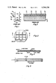
In the drawing, some figures of which are not to scale:
FIG. 1 is a schematic showing of a known charge-coupled device (CCD) imager of the field transfer type;
FIG. 2 is a section through the imager of FIG. 1 showing the electrode structure;
FIG. 3 is a plan view of a wafer containing a plurality of imagers which may be of the type shown in FIG. 1;
FIG. 4 is a section taken along line 4--4 of FIG. 3;
FIG. 5 shows some of the dimensions involved in producing one possible configuration of thinned substrate imagers;
FIGS. 6A-6E illustrate steps in a manufacturing process, embodying the invention, for making thinned imagers;
FIGS. 7A-7B illustrate the first two steps in the manufacturing process of FIG. 6, but using a masking fixture rather than a resist;
FIG. 8 is a section through a device made according to the invention, illustrating various antireflection coatings;
FIG. 9 illustrates the construction of a silicon vidicon target made according to the method of the invention; and
FIG. 10 illustrates a vidicon with the target of FIG. 9 in place.
FIG. 1 illustrates a charge-coupled device (CCD) imager of the so-called field transfer type. Such an imager is available commercially from RCA Corporation and it is known as the SID 52501.
The imager of FIG. 1 includes a photosensing array 10, known as an A register, a temporary storage array 12, known as a B register, and an output register 14, known as a C register. The B and C registers are masked, that is, means (not shown) are provided for preventing a radiant energy image from reaching either register.
The A and B registers have channel stops (not shown) extending in the column direction to isolate the channels (the columns of the CCD) from one another. The electrodes (shown in FIG. 2) may be of the single layer type comprising, for example, N+ type regions of polysilicon separated by P-type regions of polysilicon. These electrodes extend in the row direction and in the example illustrated, are three-phase operated. The electrodes are insulated from the relatively thick P-type substrate by a layer of silicon dioxide (SiO2). The SID imager mentioned above has 320 columns and 512 rows (256 in the A register and 256 in the B register), each row comprising a group of three electrodes.
The operation of the imager of FIG. 1 is well understood. During the so-called integration time, a scene or other image is projected onto the A register. The light or other radiant energy of the image causes charges to be produced at the various locations of the A register, in accordance with the light intensity reaching the respective locations.
Upon the completion of the integration time (e.g., during the vertical blanking interval of commercial television), the charge signals which have accumulated (a "field") are transferred, in parallel, in the column direction from the A to the B register by the application of the multiple phase voltages φAl . . . φA3 and φB1 . . . φB3. The charges subsequently are transferred a row at a time, from the B register to the C register, and after each row of charges reaches the C register, it is serially shifted out of the C register in response to the shift voltages φC1 . . . φC3. The transfer of charges from the B to the C register occurs during a relatively short time (the horizontal blanking time of commercial television, which is about 10 μs) and the serial shifting of the C register occurs at relatively high speed (during the horizontal line display time of commercial television). During the transfer of a field from the B to the C register, a new field may be integrated in the A register.
For a black and white imager, the illumination of the A register occurs through the single layer electrode structure. However, if one desires to sense color information, then illumination in this way is not entirely suitable because the electrodes have high absorption at the blue end of the spectrum. For such an imager it is necessary to thin the substrate and illuminate through the back surface of the thinned substrate.
In one practical approach to thinning substrates which has been employed by RCA, the number of CCD imager devices produced on a wafer is relatively small. First, using a two-inch wafer, up to three such devices, each about 0.5"×0.8", as shown in FIG. 1, are fabricated at the same time on a common substrate, employing photolithographic techniques. Then two of the three devices are masked, that is, except for the back surface of the device being thinned, the entire wafer is coated with a substance (a "resist") which is not attached by the chemical bath (an acid) used to thin the substrate. Then the entire wafer is immersed in the thinning bath and the wafer is spun about an axis passing through the center of the device being thinned. After the desired amount of thinning of the device is obtained, the wafer is removed from the bath, the resist is removed, and then the masking and other processing steps are repeated for each additional device. Then the wafer is cut apart in such a way that there is a thick substrate border surrounding the thin region of each device. This thick border provides some stiffness and mechanical support for the relatively fragile thinned substrate region.
While the process above has resulted in the production of many operational imagers (chips), it is not without its problems. One is that it is difficult to obtain uniform thinning throughout the entire imaging portion (A register) of the device. It is thought that because of the rectangular shape of the imager device, the acid bath sometimes does not attack as strongly some of the edge and corner regions of the device as the center of the device and these edges and corners therefore are sometimes thicker in the final product than the center regions of the device. Such non-uniformity is undesirable as it sometimes causes non-uniformities in the picture information produced by the imager. Also, as a practical matter, one cannot manufacture at the same time a large number of devices on the same wafer, even a large wafer. If one were to employ a larger wafer say 4" or 5" in diameter, there would be problems in spinning the wafer during thinning about an axis considerably displaced from the center of the wafer and therefore it would be difficult to utilize the outer edge portion of the wafer (recall that the axis about which the spinning takes place passes through the center of the region being thinned). In addition, the yield using this method is not as high as desired. Also, because of the fragility of the thinned substrate, it is very difficult to test the devices after they are thinned. The reason is that the test probes tend to cause the thinned substrate to become broken or otherwise damaged.
The method of manufacture embodying the present invention permits numerous thinned images to be made on a single large wafer and then to be easily tested, cut out and mounted with little risk of breakage. According to this method, a relatively large (say from 2" to 5") silicon wafer with proper impurity doping is processed in the conventional way, using photolithographic techniques, to produce a relatively large number of imagers on the common thick substrate. The front surface (the surface containing the electrodes) of the wafer may now be coated with a "resist"--a substance impervious to the bath, such as an acid bath, used for thinning, as may the peripheral edge of the back surface of the wafer as shown in FIG. 6A.
Alternatively, the wafer may be inserted into a fixture which protects the device from the acid bath in those areas where no etching is desired, as shown in FIG. 7A. The fixture includes a cap 30 and a base 32, both resistant to the acid. The wafer to be thinned is clamped at its peripheral edge between the inner peripheral notched portion 36 of the base and the inner peripheral lip 38 of the cap. The surface 40 to be thinned is exposed and the "front" surface of the chip is protected; it faces the cavity 42 within the holder. The seal between the wafer and holder is tight and prevents the acid from entering the cavity 42. To provide further protection, the cavity may be filled with water prior to sealing the wafer in the holder so that any acid which might leak into the cavity would be diluted and would not damage the devices.
Now instead of thinning the individual imagers one at a time, as in the previous process described above, the entire wafer is thinned in a rotary etching bath to the desired thickness over its entire center area, leaving only an unthinned rim around the peripheral edge of the wafer, for support, as shown in FIGS. 4, 5, 6B and 7B.
There are many possible bath mixtures which might be used as an etchant. One composition which has been found to be suitable has the following composition: 1 part hydrofluoric acid; 3 parts acetic acid; 6 parts nitric acid; bath temperature of 30° C.; etch time of 40-60 mins. The invention, of course, is not restricted to this particular bath or even to an acid bath as in some applications (depending upon the wafer material), one might use a strong base as a thinning bath.
FIG. 3 is a plan view of the wafer, each rectangle representing a complete imager device as shown in FIG. 1. As implied by the term "rotary," during the thinning process the wafer is spun about an axis perpendicular to the wafer surface and passing through the center of the wafer. As the wafer is round, and as there are no corners to create uniformity problems, it is possible, using this method, to obtain relatively uniform thinning. The wafer may be thinned to about 8-10 micrometers (μm) (25.4 μm=1 mil), that is, to roughly 1/3 of a mil.
The wafer is then removed from the thinning bath and, if using a resist, the resist is removed by standard techniques, or if using a special fixture, the wafer is removed from the fixture.
Next the thinned back surface is processed both to improve its electrical and optical characteristics. For the former, a surface layer of impurities of the same type as in the bulk is diffused or implanted into the back surface to make the surface more highly doped than the bulk of the substrate. The effect is to create a potential barrier region at the back surface to lessen the tendency of photogenerated carriers to recombine at this surface. Next an anti-reflection layer may be applied to the back surface which matches the optical character of the adhesive to be discussed next. The glass disk 20 discussed above, in one practical application, is found to have the same index of refraction as the adhesive so that the surface of the glass disk which will be adjacent the back surface of the substrate need not be coated. The other surface of the glass disk--the one interfacing with air, is coated with an anti-reflection coating. This is a standard coating used in optical products, such as lenses, and the glass disk 20 can be ordered this way. While not essential, the use of the anti-reflection coatings on the back surface of the substrate and on the exposed surface of the glass disk 20 reduces the light losses through reflection and thereby improves the sensitivity of the imager. After processing the back surface of the thinned substrate, a liquid adhesive such as epoxy is placed at the center of the thinned back surface of the wafer, the back surface facing up at this time as shown in FIG. 6C. Then a circular piece of glass 20 which fits relatively closely into the thinned region, is placed over the thinned region as also shown in FIG. 6C. In one practical approach illustrated in FIG. 5, a glass disk about 10 mils thick was used for a wafer of about 12 mils thickness, although these sizes are not critical. The 10 mils thick glass is commercially available and this is one reason it is used. In another example, the glass employed is substantially thicker (about 20 mils) and extends well beyond the rim.
After the adhesive is in place, the sandwich structure may be placed in a press and pressure applied to the glass as indicated by arrows 22 in FIG. 6C. This forces the adhesive to flow across the entire surface of the glass. The adhesive, as it flows outward, drives out all air bubbles and results in a thin transparent membrane between the glass and the thinned portion of the wafer. The pressing operation is best performed in a vacuum to assist in removing all voids and bubbles from between the glass and the silicon interface. The liquid adhesive is then allowed to cure and harden, thereby producing a mechanically strong, laminated structure as shown in FIG. 6D.
After the glue has cured, the resulting laminated structure is very strong and very rigid. It is now possible to use a conventional probe station to test the individual imager devices without worrying about cracking or otherwise damaging the thinned substrate.
After the testing step, the individual chips, that is, the individual imager devices, each consisting of a thinned device adhering to a glass backing, may be cut apart using a conventional dicing saw, 24 as shown in FIG. 6D. The dashed lines 26 in FIGS. 3 and 6D (which are legended "saw kerf" in FIG. 3) show where other cuts are made. The cut out devices, one of which is shown in larger scale in FIG. 6E than in FIGS. 6A-6D, have sufficient strength to withstand normal mounting and handling stresses with little danger of breakage, and because the glass and adhesive are essentially colorless and highly transparent, there is substantially no loss of photosensitivity due to the presence of the glass and adhesive. In other words, the presence of the glass and the adhesive does not adversely affect the performance of the imager. Nor do the glass and adhesive adversely affect the blue sensitivity of the imager (assuming, of course, that the glass chosen is itself transparent to the blue end of the spectrum as is the case in practice). Insofar as the glue is concerned, the thickness of the glue layer is extremely small and it has little effect on the color sensitivity of the imager especially if the mating surfaces of the glass and silicon substrate are treated with an anti-reflection coating, as already discussed.
FIG. 8, which is not shown to scale, shows the anti-reflection coatings. The silicon of the thinned chip 34 has an index of refraction of about 3.6. The layer 44 of material deposited thereon has a thickness of about one quarter wavelength and is chosen to have an index of refraction, such as 1.95, which is between that of the adhesive 46 and that of silicon. A suitable material is silicon monoxide. The adhesive (an epoxy) has an index of refraction of 1.51 and its thickness is such as to terminate the optical stack. The glass 48 has an index of refraction of about 1.5 so that no coating is needed at the adhesive-glass interface. The glass is purchased with a commercially applied coating 50, such as used on lenses, which reduces the reflectance at the glass-air interface.
While the present method has been described in terms of a CCD imager of the field transfer type, it is to be appreciated that is is also applicable to other forms of CCD imagers, to other forms (non CCD) of solid state imagers, and also to camera tube targets such as silicon vidicon targets. FIG. 9 illustrates the construction of such a target. The silicon target 52 is thinned in the same way as discussed above and is laminated onto the glass substrate 54 also in the same way as already discussed. The retaining rings 56, 58 hold the laminated structure 60 in place in the mounting fixture 62, 64. The vidicon with the laminated structure 60 in place, is shown schematically in FIG. 10, the glass layer facing the tube envelope and the silicon target facing the electron gun so that, in operation, it is scanned by the electron beam.
Claims (13)
1. A method of manufacturing thinned substrate imagers comprising the steps of:
masking one surface, hereafter termed the "front surface" and the peripheral edge of the opposite surface, hereafter termed the "back surface" of a wafer formed of the substrate to prevent attack by the thinning bath described in the following step:
placing the wafer in a thinning bath which attacks that part of the wafer which is not masked, for a length of time sufficient to remove the unmasked portion of the back surface to a desired depth, whereby there remains a thinned wafer with an unthinned rim around its peripheral edge;
removing the thinned wafer from the bath; and
glueing to the thinned region of the back surface of the wafer, a sheet of glass which fits into wafer within the unthinned rim thereof.
2. The method of claim 1 wherein the wafer comprises one formed of silicon.
3. The method of claim 1 wherein the sheet of glass, when in place in the thinned region of the wafer, is of a thickness roughly comparable to the thickness of substrate removed from the back surface of the wafer during the thinning process.
4. The method of claim 1 wherein the sheet of glass, when in place in the thinned region of the wafer, is of a thickness which is substantially greater than the thickness of the substrate removed from the back surface of the wafer during the thinning process.
5. The method of claim 1 wherein the wafer is not more than about 15 mils thick, before thinning, and is thinned to a fraction of a mil.
6. The method of claim 1 wherein the glueing step is carried out in a vacuum while applying pressure to the glass.
7. The method as set forth in claim 1 wherein, during thinning, the wafer is spun about an axis passing through the center portion of the wafer and perpendicular to its surfaces.
8. The method as set forth in claim 1, wherein the front surface of the wafer is formed with a plurality of imager devices thereon, and further including the step of:
cutting apart the laminated structure produced by following the steps of claim 1 along lines between the imager devices to thereby produce a plurality of devices, each comprising an imager device with thinned substrate laminated to a glass sheet glued to the back surface of a device.
9. The method as set forth in claim 8 wherein the imager devices comprise charge-coupled devices.
10. The method as set forth in claim 8 wherein the imager devices comprise silicon vidicon targets.
11. The method as set forth in claim 8 wherein said wafer is round, said thinning bath comprises an acid bath, and wherein, while the wafer is in the bath, it is spun about an axis passing through the center of the wafer and perpendicular to the surface of the wafer.
12. The method as set forth in claim 1, including the further step, after the thinning step and before the glueing step of:
placing a coating of material on the back surface of the thinned wafer having an index of refraction of a value between that of the wafer and that of the glue and a thickness such as to substantially reduce reflection of light from the glue-substrate interface.
13. The method as set forth in claim 8, including the further step, after the thinning step and before the glueing step of:
placing a coating of material on the back surface of the thinned wafer having an index of refraction of a value between that of the wafer and that of the glue and a thickness such as to substantially reduce reflection of light from the glue-substrate interface.
Priority Applications (4)
| Application Number | Priority Date | Filing Date | Title |
|---|---|---|---|
| GB8023991A GB2056172B (en) | 1979-07-25 | 1980-07-22 | Manufacture of thinned substrate imagers |
| DE19803028117 DE3028117C2 (en) | 1979-07-25 | 1980-07-24 | A method of making thin substrate image pickup devices and using this method |
| NL8004265A NL8004265A (en) | 1979-07-25 | 1980-07-24 | METHOD FOR MANUFACTURING AN IMAGE DEVICE |
| FR8016371A FR2462828B1 (en) | 1979-07-25 | 1980-07-24 | METHOD FOR MANUFACTURING IMAGING DEVICES WITH THINNED SUBSTRATE FOR TELEVISION ANALYZER TUBE FOR EXAMPLE |
Applications Claiming Priority (2)
| Application Number | Priority Date | Filing Date | Title |
|---|---|---|---|
| GB25870/79 | 1979-07-25 | ||
| GB7925870 | 1979-07-25 |
Publications (1)
| Publication Number | Publication Date |
|---|---|
| US4266334A true US4266334A (en) | 1981-05-12 |
Family
ID=10506750
Family Applications (1)
| Application Number | Title | Priority Date | Filing Date |
|---|---|---|---|
| US06/098,699 Expired - Lifetime US4266334A (en) | 1979-07-25 | 1979-11-29 | Manufacture of thinned substrate imagers |
Country Status (2)
| Country | Link |
|---|---|
| US (1) | US4266334A (en) |
| JP (1) | JPS5812747B2 (en) |
Cited By (53)
| Publication number | Priority date | Publication date | Assignee | Title |
|---|---|---|---|---|
| US4465549A (en) * | 1984-01-26 | 1984-08-14 | Rca Corporation | Method of removing a glass backing plate from one major surface of a semiconductor wafer |
| US4468857A (en) * | 1983-06-27 | 1984-09-04 | Teletype Corporation | Method of manufacturing an integrated circuit device |
| US4472875A (en) * | 1983-06-27 | 1984-09-25 | Teletype Corporation | Method for manufacturing an integrated circuit device |
| US4485553A (en) * | 1983-06-27 | 1984-12-04 | Teletype Corporation | Method for manufacturing an integrated circuit device |
| DE3534186A1 (en) * | 1984-09-26 | 1986-04-03 | Rca Corp., Princeton, N.J. | STRUCTURE FOR A SOLID IMAGE TRANSDUCER |
| US4585513A (en) * | 1985-01-30 | 1986-04-29 | Rca Corporation | Method for removing glass support from semiconductor device |
| US4599970A (en) * | 1985-03-11 | 1986-07-15 | Rca Corporation | Apparatus for coating a selected area of the surface of an object |
| US4604519A (en) * | 1983-05-13 | 1986-08-05 | Rca Corporation | Intensified charge coupled image sensor having an improved CCD support |
| GB2170651A (en) * | 1985-01-17 | 1986-08-06 | Rca Corp | Method and apparatus for aligning a filter onto a color charge-coupled device imager |
| US4623608A (en) * | 1985-03-14 | 1986-11-18 | Rca Corporation | Method and apparatus for coating a selected area of the surface of an object |
| US4633076A (en) * | 1985-02-26 | 1986-12-30 | Rca Corporation | Intensified charge-coupled image sensor having a header assembly with an eccentrically disposed CCD support assembly therein |
| US4639590A (en) * | 1985-02-26 | 1987-01-27 | Rca Corporation | Intensified charge-coupled image sensor having a charge-coupled device with contact pads on an annular rim thereof |
| US4654681A (en) * | 1985-10-01 | 1987-03-31 | Rca Corporation | Arrangement of semiconductor devices on a wafer |
| US4659226A (en) * | 1985-12-04 | 1987-04-21 | Rca Corporation | Method of making a semiconductor device |
| US4716447A (en) * | 1985-09-20 | 1987-12-29 | Rca Corporation | Interrupting charge integration in semiconductor imagers exposed to radiant energy |
| US4729971A (en) * | 1987-03-31 | 1988-03-08 | Microwave Semiconductor Corporation | Semiconductor wafer dicing techniques |
| US4822748A (en) * | 1984-08-20 | 1989-04-18 | California Institute Of Technology | Photosensor with enhanced quantum efficiency |
| US4853763A (en) * | 1984-06-27 | 1989-08-01 | The Bergquist Company | Mounting base pad means for semiconductor devices and method of preparing same |
| US4891334A (en) * | 1987-11-10 | 1990-01-02 | Nippon Zeon Co., Ltd. | Process for production of electronic devices utilizing novolak resin as protective material |
| US4914815A (en) * | 1988-02-23 | 1990-04-10 | Mitsubishi Denki Kabushiki Kaisha | Method for manufacturing hybrid integrated circuits |
| US5087585A (en) * | 1989-07-11 | 1992-02-11 | Nec Corporation | Method of stacking semiconductor substrates for fabrication of three-dimensional integrated circuit |
| US5162251A (en) * | 1991-03-18 | 1992-11-10 | Hughes Danbury Optical Systems, Inc. | Method for making thinned charge-coupled devices |
| US5227313A (en) * | 1992-07-24 | 1993-07-13 | Eastman Kodak Company | Process for making backside illuminated image sensors |
| US5234860A (en) * | 1992-03-19 | 1993-08-10 | Eastman Kodak Company | Thinning of imaging device processed wafers |
| US5244817A (en) * | 1992-08-03 | 1993-09-14 | Eastman Kodak Company | Method of making backside illuminated image sensors |
| EP0585125A2 (en) * | 1992-08-26 | 1994-03-02 | Seiko Instruments Inc. | A thin film semiconductor device and method of manufacture |
| US5480842A (en) * | 1994-04-11 | 1996-01-02 | At&T Corp. | Method for fabricating thin, strong, and flexible die for smart cards |
| DE19547284C1 (en) * | 1995-12-18 | 1996-12-19 | Siemens Ag | Thinned semiconductor wafer processing method |
| US5786988A (en) * | 1996-07-02 | 1998-07-28 | Sandisk Corporation | Integrated circuit chips made bendable by forming indentations in their back surfaces flexible packages thereof and methods of manufacture |
| US5851845A (en) * | 1995-12-18 | 1998-12-22 | Micron Technology, Inc. | Process for packaging a semiconductor die using dicing and testing |
| WO1999009589A1 (en) * | 1997-08-19 | 1999-02-25 | Siemens Aktiengesellschaft | Method for making thin slices, in particular wafers, and resulting thin slices |
| EP0933822A2 (en) * | 1998-01-20 | 1999-08-04 | Sharp Kabushiki Kaisha | Substrate for forming high-strenght thin semiconductor element and method for manufacturing high-strength thin semiconductor element |
| US6017822A (en) * | 1998-09-16 | 2000-01-25 | The United States Of America As Represented By The National Security Agency | Method of thinning semiconductor wafer of smaller diameter than thinning equipment was designed for |
| US6033489A (en) * | 1998-05-29 | 2000-03-07 | Fairchild Semiconductor Corp. | Semiconductor substrate and method of making same |
| US6165815A (en) * | 1996-02-20 | 2000-12-26 | Micron Technology, Inc. | Method of fabrication of stacked semiconductor devices |
| US6286499B1 (en) * | 1998-10-14 | 2001-09-11 | Disco Corporation | Method of cutting and separating a bent board into individual small divisions |
| US6433360B1 (en) * | 1999-01-15 | 2002-08-13 | Xilinx, Inc. | Structure and method of testing failed or returned die to determine failure location and type |
| US20050009236A1 (en) * | 1996-05-20 | 2005-01-13 | Ball Michael B. | Method of fabrication of stacked semiconductor devices |
| US6869894B2 (en) | 2002-12-20 | 2005-03-22 | General Chemical Corporation | Spin-on adhesive for temporary wafer coating and mounting to support wafer thinning and backside processing |
| US20050064679A1 (en) * | 2003-09-19 | 2005-03-24 | Farnworth Warren M. | Consolidatable composite materials, articles of manufacture formed therefrom, and fabrication methods |
| US20050064683A1 (en) * | 2003-09-19 | 2005-03-24 | Farnworth Warren M. | Method and apparatus for supporting wafers for die singulation and subsequent handling |
| US20050064681A1 (en) * | 2003-09-19 | 2005-03-24 | Wood Alan G. | Support structure for thinning semiconductor substrates and thinning methods employing the support structure |
| US20050245005A1 (en) * | 2004-04-29 | 2005-11-03 | Benson Peter A | Wafer edge ring structures and methods of formation |
| US20060049632A1 (en) * | 2001-02-06 | 2006-03-09 | Williams Peter C | Tube fitting for stainless steel tubing |
| US20060087007A1 (en) * | 2004-10-26 | 2006-04-27 | Dainippon Screen Mfg. Co., Ltd. | Wafer treating apparatus and method |
| EP1799446A2 (en) * | 2004-08-20 | 2007-06-27 | Semitool, Inc. | System for thinning a semiconductor workpiece |
| KR100769742B1 (en) * | 1999-06-17 | 2007-10-24 | 페어차일드 세미컨덕터 코포레이션 | Self-Supported Ultra Thin Silicon Wafer Process |
| US20090152534A1 (en) * | 2007-12-18 | 2009-06-18 | Chabinyc Michael L | Producing Layered Structures With Lamination |
| US20090251879A1 (en) * | 2008-04-04 | 2009-10-08 | Thompson Jeffrey C | Die thinning processes and structures |
| US20090250249A1 (en) * | 2008-04-04 | 2009-10-08 | Racz Livia M | Interposers, electronic modules, and methods for forming the same |
| US20090250823A1 (en) * | 2008-04-04 | 2009-10-08 | Racz Livia M | Electronic Modules and Methods for Forming the Same |
| US20120138959A1 (en) * | 2010-12-01 | 2012-06-07 | Hon Hai Precision Industry Co., Ltd. | Light emitting diode with a stable color temperature |
| US20130217185A1 (en) * | 2012-02-20 | 2013-08-22 | Ixys Corporation | Power device manufacture on the recessed side of a thinned wafer |
Families Citing this family (2)
| Publication number | Priority date | Publication date | Assignee | Title |
|---|---|---|---|---|
| JPS60120801U (en) * | 1984-01-25 | 1985-08-15 | 小松ゼノア株式会社 | Chain saw vibration isolation device |
| JPS6185177A (en) * | 1984-10-03 | 1986-04-30 | Ensuikou Seito Kk | Pulverization or granulation of nut |
Citations (8)
| Publication number | Priority date | Publication date | Assignee | Title |
|---|---|---|---|---|
| US3800194A (en) * | 1972-04-07 | 1974-03-26 | Hitachi Ltd | Photoconductive target of an image tube |
| US3864819A (en) * | 1970-12-07 | 1975-02-11 | Hughes Aircraft Co | Method for fabricating semiconductor devices |
| US3900882A (en) * | 1973-03-30 | 1975-08-19 | Matsushita Electric Ind Co Ltd | Photoconductor element |
| US3966512A (en) * | 1973-09-10 | 1976-06-29 | Hitachi, Ltd. | Method of manufacturing targets of pickup tubes |
| US4007473A (en) * | 1974-06-21 | 1977-02-08 | Hitachi, Ltd. | Target structures for use in photoconductive image pickup tubes and method of manufacturing the same |
| US4029394A (en) * | 1974-05-16 | 1977-06-14 | Minolta Camera Kabushiki Kaisha | Color encoding filter and method for making the same |
| US4068253A (en) * | 1975-08-20 | 1978-01-10 | Matsushita Electric Industrial Co., Ltd. | Photoconductor element and method of making the element |
| US4099198A (en) * | 1975-05-14 | 1978-07-04 | English Electric Valve Company Limited | Photocathodes |
-
1979
- 1979-11-29 US US06/098,699 patent/US4266334A/en not_active Expired - Lifetime
-
1980
- 1980-07-22 JP JP55101041A patent/JPS5812747B2/en not_active Expired
Patent Citations (8)
| Publication number | Priority date | Publication date | Assignee | Title |
|---|---|---|---|---|
| US3864819A (en) * | 1970-12-07 | 1975-02-11 | Hughes Aircraft Co | Method for fabricating semiconductor devices |
| US3800194A (en) * | 1972-04-07 | 1974-03-26 | Hitachi Ltd | Photoconductive target of an image tube |
| US3900882A (en) * | 1973-03-30 | 1975-08-19 | Matsushita Electric Ind Co Ltd | Photoconductor element |
| US3966512A (en) * | 1973-09-10 | 1976-06-29 | Hitachi, Ltd. | Method of manufacturing targets of pickup tubes |
| US4029394A (en) * | 1974-05-16 | 1977-06-14 | Minolta Camera Kabushiki Kaisha | Color encoding filter and method for making the same |
| US4007473A (en) * | 1974-06-21 | 1977-02-08 | Hitachi, Ltd. | Target structures for use in photoconductive image pickup tubes and method of manufacturing the same |
| US4099198A (en) * | 1975-05-14 | 1978-07-04 | English Electric Valve Company Limited | Photocathodes |
| US4068253A (en) * | 1975-08-20 | 1978-01-10 | Matsushita Electric Industrial Co., Ltd. | Photoconductor element and method of making the element |
Non-Patent Citations (2)
| Title |
|---|
| Antcliffe et al., A Backside Illuminated 400.times.400 Charge-Coupled Device Imager, IEEE Trans. on Electron Devices, vol. ED-23, No. 11, Nov. 1976, pp. 1225-1232. * |
| Antcliffe et al., A Backside Illuminated 400×400 Charge-Coupled Device Imager, IEEE Trans. on Electron Devices, vol. ED-23, No. 11, Nov. 1976, pp. 1225-1232. |
Cited By (82)
| Publication number | Priority date | Publication date | Assignee | Title |
|---|---|---|---|---|
| US4604519A (en) * | 1983-05-13 | 1986-08-05 | Rca Corporation | Intensified charge coupled image sensor having an improved CCD support |
| US4468857A (en) * | 1983-06-27 | 1984-09-04 | Teletype Corporation | Method of manufacturing an integrated circuit device |
| US4472875A (en) * | 1983-06-27 | 1984-09-25 | Teletype Corporation | Method for manufacturing an integrated circuit device |
| US4485553A (en) * | 1983-06-27 | 1984-12-04 | Teletype Corporation | Method for manufacturing an integrated circuit device |
| US4465549A (en) * | 1984-01-26 | 1984-08-14 | Rca Corporation | Method of removing a glass backing plate from one major surface of a semiconductor wafer |
| US4853763A (en) * | 1984-06-27 | 1989-08-01 | The Bergquist Company | Mounting base pad means for semiconductor devices and method of preparing same |
| US4822748A (en) * | 1984-08-20 | 1989-04-18 | California Institute Of Technology | Photosensor with enhanced quantum efficiency |
| US4622580A (en) * | 1984-09-26 | 1986-11-11 | Rca Corporation | Solid-state imager chip mounting |
| DE3534186A1 (en) * | 1984-09-26 | 1986-04-03 | Rca Corp., Princeton, N.J. | STRUCTURE FOR A SOLID IMAGE TRANSDUCER |
| GB2170651A (en) * | 1985-01-17 | 1986-08-06 | Rca Corp | Method and apparatus for aligning a filter onto a color charge-coupled device imager |
| US4585513A (en) * | 1985-01-30 | 1986-04-29 | Rca Corporation | Method for removing glass support from semiconductor device |
| US4633076A (en) * | 1985-02-26 | 1986-12-30 | Rca Corporation | Intensified charge-coupled image sensor having a header assembly with an eccentrically disposed CCD support assembly therein |
| US4639590A (en) * | 1985-02-26 | 1987-01-27 | Rca Corporation | Intensified charge-coupled image sensor having a charge-coupled device with contact pads on an annular rim thereof |
| US4599970A (en) * | 1985-03-11 | 1986-07-15 | Rca Corporation | Apparatus for coating a selected area of the surface of an object |
| US4623608A (en) * | 1985-03-14 | 1986-11-18 | Rca Corporation | Method and apparatus for coating a selected area of the surface of an object |
| US4716447A (en) * | 1985-09-20 | 1987-12-29 | Rca Corporation | Interrupting charge integration in semiconductor imagers exposed to radiant energy |
| US4654681A (en) * | 1985-10-01 | 1987-03-31 | Rca Corporation | Arrangement of semiconductor devices on a wafer |
| US4659226A (en) * | 1985-12-04 | 1987-04-21 | Rca Corporation | Method of making a semiconductor device |
| US4729971A (en) * | 1987-03-31 | 1988-03-08 | Microwave Semiconductor Corporation | Semiconductor wafer dicing techniques |
| US4891334A (en) * | 1987-11-10 | 1990-01-02 | Nippon Zeon Co., Ltd. | Process for production of electronic devices utilizing novolak resin as protective material |
| US4914815A (en) * | 1988-02-23 | 1990-04-10 | Mitsubishi Denki Kabushiki Kaisha | Method for manufacturing hybrid integrated circuits |
| US5087585A (en) * | 1989-07-11 | 1992-02-11 | Nec Corporation | Method of stacking semiconductor substrates for fabrication of three-dimensional integrated circuit |
| US5162251A (en) * | 1991-03-18 | 1992-11-10 | Hughes Danbury Optical Systems, Inc. | Method for making thinned charge-coupled devices |
| US5234860A (en) * | 1992-03-19 | 1993-08-10 | Eastman Kodak Company | Thinning of imaging device processed wafers |
| US5227313A (en) * | 1992-07-24 | 1993-07-13 | Eastman Kodak Company | Process for making backside illuminated image sensors |
| US5244817A (en) * | 1992-08-03 | 1993-09-14 | Eastman Kodak Company | Method of making backside illuminated image sensors |
| EP0585125A3 (en) * | 1992-08-26 | 1997-09-10 | Seiko Instr Inc | A thin film semiconductor device and method of manufacture |
| EP0585125A2 (en) * | 1992-08-26 | 1994-03-02 | Seiko Instruments Inc. | A thin film semiconductor device and method of manufacture |
| US5480842A (en) * | 1994-04-11 | 1996-01-02 | At&T Corp. | Method for fabricating thin, strong, and flexible die for smart cards |
| US5851845A (en) * | 1995-12-18 | 1998-12-22 | Micron Technology, Inc. | Process for packaging a semiconductor die using dicing and testing |
| DE19547284C1 (en) * | 1995-12-18 | 1996-12-19 | Siemens Ag | Thinned semiconductor wafer processing method |
| US6165815A (en) * | 1996-02-20 | 2000-12-26 | Micron Technology, Inc. | Method of fabrication of stacked semiconductor devices |
| US6989285B2 (en) | 1996-05-20 | 2006-01-24 | Micron Technology, Inc. | Method of fabrication of stacked semiconductor devices |
| US20050009236A1 (en) * | 1996-05-20 | 2005-01-13 | Ball Michael B. | Method of fabrication of stacked semiconductor devices |
| US7371612B2 (en) | 1996-05-20 | 2008-05-13 | Micron Technology, Inc. | Method of fabrication of stacked semiconductor devices |
| US5786988A (en) * | 1996-07-02 | 1998-07-28 | Sandisk Corporation | Integrated circuit chips made bendable by forming indentations in their back surfaces flexible packages thereof and methods of manufacture |
| WO1999009589A1 (en) * | 1997-08-19 | 1999-02-25 | Siemens Aktiengesellschaft | Method for making thin slices, in particular wafers, and resulting thin slices |
| EP0933822A2 (en) * | 1998-01-20 | 1999-08-04 | Sharp Kabushiki Kaisha | Substrate for forming high-strenght thin semiconductor element and method for manufacturing high-strength thin semiconductor element |
| EP0933822A3 (en) * | 1998-01-20 | 1999-12-15 | Sharp Kabushiki Kaisha | Substrate for forming high-strenght thin semiconductor element and method for manufacturing high-strength thin semiconductor element |
| US6033489A (en) * | 1998-05-29 | 2000-03-07 | Fairchild Semiconductor Corp. | Semiconductor substrate and method of making same |
| US6017822A (en) * | 1998-09-16 | 2000-01-25 | The United States Of America As Represented By The National Security Agency | Method of thinning semiconductor wafer of smaller diameter than thinning equipment was designed for |
| SG85152A1 (en) * | 1998-10-14 | 2001-12-19 | Disco Corp | Method of cutting and separating a bent board into individual small divisions |
| US6286499B1 (en) * | 1998-10-14 | 2001-09-11 | Disco Corporation | Method of cutting and separating a bent board into individual small divisions |
| US6433360B1 (en) * | 1999-01-15 | 2002-08-13 | Xilinx, Inc. | Structure and method of testing failed or returned die to determine failure location and type |
| US6768329B1 (en) | 1999-01-15 | 2004-07-27 | Xilinx Inc. | Structure and method of testing failed or returned die to determine failure location and type |
| KR100769742B1 (en) * | 1999-06-17 | 2007-10-24 | 페어차일드 세미컨덕터 코포레이션 | Self-Supported Ultra Thin Silicon Wafer Process |
| US20060049632A1 (en) * | 2001-02-06 | 2006-03-09 | Williams Peter C | Tube fitting for stainless steel tubing |
| US6869894B2 (en) | 2002-12-20 | 2005-03-22 | General Chemical Corporation | Spin-on adhesive for temporary wafer coating and mounting to support wafer thinning and backside processing |
| US7098152B2 (en) | 2002-12-20 | 2006-08-29 | General Chemical Performance Products, Llc | Adhesive support method for wafer coating, thinning and backside processing |
| US20060003549A1 (en) * | 2003-09-19 | 2006-01-05 | Wood Alan G | Assemblies including semiconductor substrates of reduced thickness and support structures therefor |
| US20050064681A1 (en) * | 2003-09-19 | 2005-03-24 | Wood Alan G. | Support structure for thinning semiconductor substrates and thinning methods employing the support structure |
| US20060003255A1 (en) * | 2003-09-19 | 2006-01-05 | Wood Alan G | Methods for optimizing physical characteristics of selectively consolidatable materials |
| US20060008739A1 (en) * | 2003-09-19 | 2006-01-12 | Wood Alan G | Materials for use in programmed material consolidation processes |
| US20050064679A1 (en) * | 2003-09-19 | 2005-03-24 | Farnworth Warren M. | Consolidatable composite materials, articles of manufacture formed therefrom, and fabrication methods |
| US7960829B2 (en) | 2003-09-19 | 2011-06-14 | Micron Technology, Inc. | Support structure for use in thinning semiconductor substrates and for supporting thinned semiconductor substrates |
| US7713841B2 (en) | 2003-09-19 | 2010-05-11 | Micron Technology, Inc. | Methods for thinning semiconductor substrates that employ support structures formed on the substrates |
| US20050064683A1 (en) * | 2003-09-19 | 2005-03-24 | Farnworth Warren M. | Method and apparatus for supporting wafers for die singulation and subsequent handling |
| US20060001139A1 (en) * | 2003-09-19 | 2006-01-05 | Wood Alan G | Support structure for use in thinning semiconductor substrates and for supporting thinned semiconductor substrates |
| US20050255675A1 (en) * | 2003-09-19 | 2005-11-17 | Farnworth Warren M | Apparatus for supporting wafers for die singulation and subsequent handling and in-process wafer structure |
| US20060192283A1 (en) * | 2004-04-29 | 2006-08-31 | Benson Peter A | Semiconductor wafer assemblies |
| US7489020B2 (en) | 2004-04-29 | 2009-02-10 | Micron Technology, Inc. | Semiconductor wafer assemblies |
| US20050245005A1 (en) * | 2004-04-29 | 2005-11-03 | Benson Peter A | Wafer edge ring structures and methods of formation |
| US7244665B2 (en) | 2004-04-29 | 2007-07-17 | Micron Technology, Inc. | Wafer edge ring structures and methods of formation |
| US20060191475A1 (en) * | 2004-04-29 | 2006-08-31 | Benson Peter A | Apparatus for spin coating semiconductor substrates |
| US7615119B2 (en) | 2004-04-29 | 2009-11-10 | Micron Technology, Inc. | Apparatus for spin coating semiconductor substrates |
| EP1799446A2 (en) * | 2004-08-20 | 2007-06-27 | Semitool, Inc. | System for thinning a semiconductor workpiece |
| EP1799446A4 (en) * | 2004-08-20 | 2010-03-03 | Semitool Inc | System for thinning a semiconductor workpiece |
| US20060087007A1 (en) * | 2004-10-26 | 2006-04-27 | Dainippon Screen Mfg. Co., Ltd. | Wafer treating apparatus and method |
| US20090152534A1 (en) * | 2007-12-18 | 2009-06-18 | Chabinyc Michael L | Producing Layered Structures With Lamination |
| US7755156B2 (en) | 2007-12-18 | 2010-07-13 | Palo Alto Research Center Incorporated | Producing layered structures with lamination |
| US20090251879A1 (en) * | 2008-04-04 | 2009-10-08 | Thompson Jeffrey C | Die thinning processes and structures |
| US20090250249A1 (en) * | 2008-04-04 | 2009-10-08 | Racz Livia M | Interposers, electronic modules, and methods for forming the same |
| US7960247B2 (en) | 2008-04-04 | 2011-06-14 | The Charles Stark Draper Laboratory, Inc. | Die thinning processes and structures |
| US8017451B2 (en) | 2008-04-04 | 2011-09-13 | The Charles Stark Draper Laboratory, Inc. | Electronic modules and methods for forming the same |
| US8273603B2 (en) | 2008-04-04 | 2012-09-25 | The Charles Stark Draper Laboratory, Inc. | Interposers, electronic modules, and methods for forming the same |
| US8535984B2 (en) | 2008-04-04 | 2013-09-17 | The Charles Stark Draper Laboratory, Inc. | Electronic modules and methods for forming the same |
| US20090250823A1 (en) * | 2008-04-04 | 2009-10-08 | Racz Livia M | Electronic Modules and Methods for Forming the Same |
| US9425069B2 (en) | 2008-04-04 | 2016-08-23 | Charles Stark Draper Laboratory, Inc. | Electronic modules |
| US20120138959A1 (en) * | 2010-12-01 | 2012-06-07 | Hon Hai Precision Industry Co., Ltd. | Light emitting diode with a stable color temperature |
| US8461599B2 (en) * | 2010-12-01 | 2013-06-11 | Hon Hai Precision Industry Co., Ltd. | Light emitting diode with a stable color temperature |
| US8716067B2 (en) * | 2012-02-20 | 2014-05-06 | Ixys Corporation | Power device manufacture on the recessed side of a thinned wafer |
| US20130217185A1 (en) * | 2012-02-20 | 2013-08-22 | Ixys Corporation | Power device manufacture on the recessed side of a thinned wafer |
Also Published As
| Publication number | Publication date |
|---|---|
| JPS5812747B2 (en) | 1983-03-10 |
| JPS5621383A (en) | 1981-02-27 |
Similar Documents
| Publication | Publication Date | Title |
|---|---|---|
| US4266334A (en) | Manufacture of thinned substrate imagers | |
| EP1961045B1 (en) | Manufacturing method of a solid state imaging device | |
| US7923798B2 (en) | Optical device and method for fabricating the same, camera module using optical device, and electronic equipment mounting camera module | |
| US20070259463A1 (en) | Wafer-level method for thinning imaging sensors for backside illumination | |
| US6498073B2 (en) | Back illuminated imager with enhanced UV to near IR sensitivity | |
| TWI467747B (en) | Solid photographic apparatus and method of manufacturing the same | |
| JP2003298035A (en) | Method for sawing wafer | |
| CN102683359A (en) | Solid-state imaging device, manufacturing method thereof, electronic apparatus, and semiconductor device | |
| US7947526B2 (en) | Method of making backside illumination image sensor | |
| GB2056172A (en) | Manufacture of thinned substrate imagers | |
| US4639590A (en) | Intensified charge-coupled image sensor having a charge-coupled device with contact pads on an annular rim thereof | |
| KR100919964B1 (en) | Color image sensor on transparent substrate and method for making same | |
| US4604519A (en) | Intensified charge coupled image sensor having an improved CCD support | |
| US4585513A (en) | Method for removing glass support from semiconductor device | |
| GB2170651A (en) | Method and apparatus for aligning a filter onto a color charge-coupled device imager | |
| CN104157662A (en) | High sensitivity image sensor pixel structure and manufacture method thereof | |
| JPS6130241B2 (en) | ||
| JPS5999763A (en) | Solid-state image-pickup device | |
| US20070166868A1 (en) | Method of fabricating an image sensor | |
| EP0203591A2 (en) | Method of reinforcing a body of silicon, materials therefor and its use in the thinning of a plate-like body of silicon | |
| JPS62262001A (en) | Solid-state color image pickup device | |
| JP4521938B2 (en) | Imaging device | |
| NL8004265A (en) | METHOD FOR MANUFACTURING AN IMAGE DEVICE | |
| EP0171801A2 (en) | Method for processing a backside illuminated detector assembly | |
| JPH0379681B2 (en) |
Legal Events
| Date | Code | Title | Description |
|---|---|---|---|
| STCF | Information on status: patent grant |
Free format text: PATENTED CASE |