US4367414A - Method and apparatus for controlling distributed electrical loads - Google Patents

Method and apparatus for controlling distributed electrical loads Download PDF

Info

Publication number
US4367414A
US4367414A US06/352,578 US35257882A US4367414A US 4367414 A US4367414 A US 4367414A US 35257882 A US35257882 A US 35257882A US 4367414 A US4367414 A US 4367414A
Authority
US
United States
Prior art keywords
data
data line
transceiver
line
controller
Prior art date
Legal status (The legal status is an assumption and is not a legal conclusion. Google has not performed a legal analysis and makes no representation as to the accuracy of the status listed.)
Expired - Fee Related
Application number
US06/352,578
Inventor
Edward B. Miller
Charles W. Eichelberger
Current Assignee (The listed assignees may be inaccurate. Google has not performed a legal analysis and makes no representation or warranty as to the accuracy of the list.)
General Electric Co
Original Assignee
General Electric Co
Priority date (The priority date is an assumption and is not a legal conclusion. Google has not performed a legal analysis and makes no representation as to the accuracy of the date listed.)
Filing date
Publication date
Application filed by General Electric Co filed Critical General Electric Co
Priority to US06/352,578 priority Critical patent/US4367414A/en
Application granted granted Critical
Publication of US4367414A publication Critical patent/US4367414A/en
Anticipated expiration legal-status Critical
Expired - Fee Related legal-status Critical Current

Links

Images

Classifications

    • HELECTRICITY
    • H05ELECTRIC TECHNIQUES NOT OTHERWISE PROVIDED FOR
    • H05BELECTRIC HEATING; ELECTRIC LIGHT SOURCES NOT OTHERWISE PROVIDED FOR; CIRCUIT ARRANGEMENTS FOR ELECTRIC LIGHT SOURCES, IN GENERAL
    • H05B47/00Circuit arrangements for operating light sources in general, i.e. where the type of light source is not relevant
    • H05B47/10Controlling the light source
    • H05B47/155Coordinated control of two or more light sources
    • HELECTRICITY
    • H02GENERATION; CONVERSION OR DISTRIBUTION OF ELECTRIC POWER
    • H02JCIRCUIT ARRANGEMENTS OR SYSTEMS FOR SUPPLYING OR DISTRIBUTING ELECTRIC POWER; SYSTEMS FOR STORING ELECTRIC ENERGY
    • H02J13/00Circuit arrangements for providing remote indication of network conditions, e.g. an instantaneous record of the open or closed condition of each circuitbreaker in the network; Circuit arrangements for providing remote control of switching means in a power distribution network, e.g. switching in and out of current consumers by using a pulse code signal carried by the network
    • H02J13/00001Circuit arrangements for providing remote indication of network conditions, e.g. an instantaneous record of the open or closed condition of each circuitbreaker in the network; Circuit arrangements for providing remote control of switching means in a power distribution network, e.g. switching in and out of current consumers by using a pulse code signal carried by the network characterised by the display of information or by user interaction, e.g. supervisory control and data acquisition systems [SCADA] or graphical user interfaces [GUI]
    • HELECTRICITY
    • H02GENERATION; CONVERSION OR DISTRIBUTION OF ELECTRIC POWER
    • H02JCIRCUIT ARRANGEMENTS OR SYSTEMS FOR SUPPLYING OR DISTRIBUTING ELECTRIC POWER; SYSTEMS FOR STORING ELECTRIC ENERGY
    • H02J13/00Circuit arrangements for providing remote indication of network conditions, e.g. an instantaneous record of the open or closed condition of each circuitbreaker in the network; Circuit arrangements for providing remote control of switching means in a power distribution network, e.g. switching in and out of current consumers by using a pulse code signal carried by the network
    • H02J13/00002Circuit arrangements for providing remote indication of network conditions, e.g. an instantaneous record of the open or closed condition of each circuitbreaker in the network; Circuit arrangements for providing remote control of switching means in a power distribution network, e.g. switching in and out of current consumers by using a pulse code signal carried by the network characterised by monitoring
    • HELECTRICITY
    • H02GENERATION; CONVERSION OR DISTRIBUTION OF ELECTRIC POWER
    • H02JCIRCUIT ARRANGEMENTS OR SYSTEMS FOR SUPPLYING OR DISTRIBUTING ELECTRIC POWER; SYSTEMS FOR STORING ELECTRIC ENERGY
    • H02J13/00Circuit arrangements for providing remote indication of network conditions, e.g. an instantaneous record of the open or closed condition of each circuitbreaker in the network; Circuit arrangements for providing remote control of switching means in a power distribution network, e.g. switching in and out of current consumers by using a pulse code signal carried by the network
    • H02J13/00006Circuit arrangements for providing remote indication of network conditions, e.g. an instantaneous record of the open or closed condition of each circuitbreaker in the network; Circuit arrangements for providing remote control of switching means in a power distribution network, e.g. switching in and out of current consumers by using a pulse code signal carried by the network characterised by information or instructions transport means between the monitoring, controlling or managing units and monitored, controlled or operated power network element or electrical equipment
    • H02J13/00016Circuit arrangements for providing remote indication of network conditions, e.g. an instantaneous record of the open or closed condition of each circuitbreaker in the network; Circuit arrangements for providing remote control of switching means in a power distribution network, e.g. switching in and out of current consumers by using a pulse code signal carried by the network characterised by information or instructions transport means between the monitoring, controlling or managing units and monitored, controlled or operated power network element or electrical equipment using a wired telecommunication network or a data transmission bus
    • HELECTRICITY
    • H02GENERATION; CONVERSION OR DISTRIBUTION OF ELECTRIC POWER
    • H02JCIRCUIT ARRANGEMENTS OR SYSTEMS FOR SUPPLYING OR DISTRIBUTING ELECTRIC POWER; SYSTEMS FOR STORING ELECTRIC ENERGY
    • H02J13/00Circuit arrangements for providing remote indication of network conditions, e.g. an instantaneous record of the open or closed condition of each circuitbreaker in the network; Circuit arrangements for providing remote control of switching means in a power distribution network, e.g. switching in and out of current consumers by using a pulse code signal carried by the network
    • H02J13/00032Systems characterised by the controlled or operated power network elements or equipment, the power network elements or equipment not otherwise provided for
    • H02J13/00036Systems characterised by the controlled or operated power network elements or equipment, the power network elements or equipment not otherwise provided for the elements or equipment being or involving switches, relays or circuit breakers
    • HELECTRICITY
    • H05ELECTRIC TECHNIQUES NOT OTHERWISE PROVIDED FOR
    • H05BELECTRIC HEATING; ELECTRIC LIGHT SOURCES NOT OTHERWISE PROVIDED FOR; CIRCUIT ARRANGEMENTS FOR ELECTRIC LIGHT SOURCES, IN GENERAL
    • H05B47/00Circuit arrangements for operating light sources in general, i.e. where the type of light source is not relevant
    • H05B47/10Controlling the light source
    • H05B47/105Controlling the light source in response to determined parameters
    • H05B47/11Controlling the light source in response to determined parameters by determining the brightness or colour temperature of ambient light
    • HELECTRICITY
    • H05ELECTRIC TECHNIQUES NOT OTHERWISE PROVIDED FOR
    • H05BELECTRIC HEATING; ELECTRIC LIGHT SOURCES NOT OTHERWISE PROVIDED FOR; CIRCUIT ARRANGEMENTS FOR ELECTRIC LIGHT SOURCES, IN GENERAL
    • H05B47/00Circuit arrangements for operating light sources in general, i.e. where the type of light source is not relevant
    • H05B47/10Controlling the light source
    • H05B47/105Controlling the light source in response to determined parameters
    • H05B47/115Controlling the light source in response to determined parameters by determining the presence or movement of objects or living beings
    • YGENERAL TAGGING OF NEW TECHNOLOGICAL DEVELOPMENTS; GENERAL TAGGING OF CROSS-SECTIONAL TECHNOLOGIES SPANNING OVER SEVERAL SECTIONS OF THE IPC; TECHNICAL SUBJECTS COVERED BY FORMER USPC CROSS-REFERENCE ART COLLECTIONS [XRACs] AND DIGESTS
    • Y02TECHNOLOGIES OR APPLICATIONS FOR MITIGATION OR ADAPTATION AGAINST CLIMATE CHANGE
    • Y02BCLIMATE CHANGE MITIGATION TECHNOLOGIES RELATED TO BUILDINGS, e.g. HOUSING, HOUSE APPLIANCES OR RELATED END-USER APPLICATIONS
    • Y02B20/00Energy efficient lighting technologies, e.g. halogen lamps or gas discharge lamps
    • Y02B20/40Control techniques providing energy savings, e.g. smart controller or presence detection
    • YGENERAL TAGGING OF NEW TECHNOLOGICAL DEVELOPMENTS; GENERAL TAGGING OF CROSS-SECTIONAL TECHNOLOGIES SPANNING OVER SEVERAL SECTIONS OF THE IPC; TECHNICAL SUBJECTS COVERED BY FORMER USPC CROSS-REFERENCE ART COLLECTIONS [XRACs] AND DIGESTS
    • Y02TECHNOLOGIES OR APPLICATIONS FOR MITIGATION OR ADAPTATION AGAINST CLIMATE CHANGE
    • Y02BCLIMATE CHANGE MITIGATION TECHNOLOGIES RELATED TO BUILDINGS, e.g. HOUSING, HOUSE APPLIANCES OR RELATED END-USER APPLICATIONS
    • Y02B70/00Technologies for an efficient end-user side electric power management and consumption
    • Y02B70/30Systems integrating technologies related to power network operation and communication or information technologies for improving the carbon footprint of the management of residential or tertiary loads, i.e. smart grids as climate change mitigation technology in the buildings sector, including also the last stages of power distribution and the control, monitoring or operating management systems at local level
    • YGENERAL TAGGING OF NEW TECHNOLOGICAL DEVELOPMENTS; GENERAL TAGGING OF CROSS-SECTIONAL TECHNOLOGIES SPANNING OVER SEVERAL SECTIONS OF THE IPC; TECHNICAL SUBJECTS COVERED BY FORMER USPC CROSS-REFERENCE ART COLLECTIONS [XRACs] AND DIGESTS
    • Y02TECHNOLOGIES OR APPLICATIONS FOR MITIGATION OR ADAPTATION AGAINST CLIMATE CHANGE
    • Y02EREDUCTION OF GREENHOUSE GAS [GHG] EMISSIONS, RELATED TO ENERGY GENERATION, TRANSMISSION OR DISTRIBUTION
    • Y02E60/00Enabling technologies; Technologies with a potential or indirect contribution to GHG emissions mitigation
    • YGENERAL TAGGING OF NEW TECHNOLOGICAL DEVELOPMENTS; GENERAL TAGGING OF CROSS-SECTIONAL TECHNOLOGIES SPANNING OVER SEVERAL SECTIONS OF THE IPC; TECHNICAL SUBJECTS COVERED BY FORMER USPC CROSS-REFERENCE ART COLLECTIONS [XRACs] AND DIGESTS
    • Y04INFORMATION OR COMMUNICATION TECHNOLOGIES HAVING AN IMPACT ON OTHER TECHNOLOGY AREAS
    • Y04SSYSTEMS INTEGRATING TECHNOLOGIES RELATED TO POWER NETWORK OPERATION, COMMUNICATION OR INFORMATION TECHNOLOGIES FOR IMPROVING THE ELECTRICAL POWER GENERATION, TRANSMISSION, DISTRIBUTION, MANAGEMENT OR USAGE, i.e. SMART GRIDS
    • Y04S10/00Systems supporting electrical power generation, transmission or distribution
    • Y04S10/18Systems supporting electrical power generation, transmission or distribution using switches, relays or circuit breakers, e.g. intelligent electronic devices [IED]
    • YGENERAL TAGGING OF NEW TECHNOLOGICAL DEVELOPMENTS; GENERAL TAGGING OF CROSS-SECTIONAL TECHNOLOGIES SPANNING OVER SEVERAL SECTIONS OF THE IPC; TECHNICAL SUBJECTS COVERED BY FORMER USPC CROSS-REFERENCE ART COLLECTIONS [XRACs] AND DIGESTS
    • Y04INFORMATION OR COMMUNICATION TECHNOLOGIES HAVING AN IMPACT ON OTHER TECHNOLOGY AREAS
    • Y04SSYSTEMS INTEGRATING TECHNOLOGIES RELATED TO POWER NETWORK OPERATION, COMMUNICATION OR INFORMATION TECHNOLOGIES FOR IMPROVING THE ELECTRICAL POWER GENERATION, TRANSMISSION, DISTRIBUTION, MANAGEMENT OR USAGE, i.e. SMART GRIDS
    • Y04S10/00Systems supporting electrical power generation, transmission or distribution
    • Y04S10/40Display of information, e.g. of data or controls
    • YGENERAL TAGGING OF NEW TECHNOLOGICAL DEVELOPMENTS; GENERAL TAGGING OF CROSS-SECTIONAL TECHNOLOGIES SPANNING OVER SEVERAL SECTIONS OF THE IPC; TECHNICAL SUBJECTS COVERED BY FORMER USPC CROSS-REFERENCE ART COLLECTIONS [XRACs] AND DIGESTS
    • Y04INFORMATION OR COMMUNICATION TECHNOLOGIES HAVING AN IMPACT ON OTHER TECHNOLOGY AREAS
    • Y04SSYSTEMS INTEGRATING TECHNOLOGIES RELATED TO POWER NETWORK OPERATION, COMMUNICATION OR INFORMATION TECHNOLOGIES FOR IMPROVING THE ELECTRICAL POWER GENERATION, TRANSMISSION, DISTRIBUTION, MANAGEMENT OR USAGE, i.e. SMART GRIDS
    • Y04S20/00Management or operation of end-user stationary applications or the last stages of power distribution; Controlling, monitoring or operating thereof
    • Y04S20/20End-user application control systems
    • Y04S20/242Home appliances
    • Y04S20/246Home appliances the system involving the remote operation of lamps or lighting equipment

Definitions

  • This invention generally relates to methods and apparatus for controlling distributed electrical loads.
  • This invention also relates to novel components, combinations and subcombinations capable of implementing such control. More particularly, it relates to a programmable microprocessor based system having a central controller under program control which communicates with plural distributed microprocessor-based transceiver decoders (also referred to as transceivers) connected together through a common communication channel (e.g. an unshielded twisted pair of wires in the presently preferred embodiment).
  • a common communication channel e.g. an unshielded twisted pair of wires in the presently preferred embodiment.
  • Remotely located switches and/or sensor devices can be employed throughout the system for modifying the nominally defined time-dependent schedule of load control functions and for rendering the system condition responsive. Control inputs may also be received at the central processor site via telephone connections.
  • the system is used to control the distributed lighting loads throughout a building, cluster of related buildings, a building site, etc.
  • the system is capable of controlling virtually any type of electrical load according to a user defined schedule and/or according to conditions sensed at remote locations.
  • loads could include heating systems, air-conditioning systems, etc.
  • Feiker was instrumental in having a first rudimentary lighting control system developed and installed in a single room at the Nela Park Plant of General Electric in Cleveland, Ohio. some of the actual design work was done by C. Eichelberger for this first rudimentary lighting control. This installation is described in the article entitled "A New Approach to Lighting System Control" by T. K. McGowan and G. E. Feiker along with some projections of alternative ways to achieve similar results.
  • One of the primary commercial applications for programmable load control is for the control of lighting, particularly for large office buildings, or groups of office buildings. Effective lighting control requires achieving the right amount of light where it is needed and when it is needed. Energy and money are wasted when there is too much or too little light for a particular task, when lights are on where not needed and when lights are not on when needed. In a typical office, lighting accounts for 30-40% of the total electrical load and in many cases a substantial amount of this light is wasted by having lights on when not needed or on at higher levels than required.
  • control of individual fixtures can allow offices, classrooms or other space to be rearranged and partitions moved without expensive, hard wiring changes. With adequate control, ceiling systems can remain unchanged even when work areas are rearranged. Furthermore, the ability to control individual fixtures also permits finely tuned lighting arrangements for different activities, for example, normal lighting or desk work; reduced lighting for conferences; and dim lighting for slides, security lighting, etc.
  • the ability to control lighting can be used to control the use of space. For example, unwanted use of an area can be minimized by not allowing the lighting to be controlled by unauthorized personnel. Thus, the use of conference rooms can be curtailed for unauthorized meetings or as temporary work areas for tasks which should be performed in offices.
  • the programmable load control system as set forth herein allows for control over these built-in energy wasting situations. It calls for the automatic shutting off of lights during the progammed non-use times while permitting selected overrides for providing light in the immediate area of a person working outside his normal hours. It allows light levels to be altered in accordance with a pre-defined schedule such that tasks performed at or during preset times requiring a lower light level than normal will not waste power. Furthermore, in areas near windows, where daylight adds a substantial amount of light, a photo relay is used to automatically reduce lighting levels when adequate sunlight is available.
  • the difference in energy cost for the normal electrical load for a typical office building and that for a building controlled by the present invention is substantial.
  • a typical payback time for the cost of installation of the control system is 1-2 years.
  • the presently described system for distributed electrical load control for lighting provides a degree of flexibility and economy not previously available with any prior system. It uses mechanically latching relays to control groups of lighting fixtures or other loads. These relays are turned on or off by a 24-volt pulse. However, the relays are not hard wired to manual switches, time switches, photocells, etc. All control comes from a central controller, through a data line to a transceiver decoder associated with the relay to be operated.
  • the central controller utilized in the present system is micro-computer based and has an internal program providing the function of a user programmable load control system. It incorporates a 7-day clock and provides minute-by-minute control of the entire load system including up to 8000 separate relays according to a predetermined schedule when operating in its automatic mode.
  • the data format selected would allow the use of up to 16,000 relays.
  • the memory space available in the memories selected for this presently preferred embodiment limits the number of relays to 8,000.
  • a load control schedule can be entered manually through a keyboard or by reading mark-sense cards through a cardreader.
  • any lighting circuit can be controlled manually from the keyboard of the central controller when operating in its manual mode.
  • the central controller also provides monitoring of the system and can display the on/off state of each relay. If hard copy records are desired, the controller can print data out through a standard printer.
  • a low voltage twisted pair data line running throughout a building under load control forms a communication channel which connects the central controller to a plurality of transceiver decoders and provides for two-way (bi-directional) communications between the controller and each of the transceiver decoders.
  • each transceiver decoder Up to 32 relays are coupled to each transceiver decoder. Each relay turns on and off a particular load in response to a command from the central controller, propagated through the data line to its associated transceiver decoder.
  • the transceiver decoder is generally located near the loads to be controlled by its relays so as to minimize the amount of hard wiring needed.
  • the transceiver decoder receives a signal from the central controller over the data line when one of its relays is to be opened or closed and transmits an activating pulse to the relay.
  • Each transceiver decoder can send a message to the controller requesting that the controller issue a command to alter the state of a particular load.
  • Each transceiver decoder has 8 switchleg inputs which can be connected to manually operable or condition responsive switches, either of the momentary or maintained contact type. Each switch can control "on” or “off” a designated subset of lighting control relays, known as a sector, anywhere in the building. This is accomplished by activating a switch causing the transceiver decoder to send a signal through the data line to the central controller. The central controller interprets that signal and determines which relays require activation and in turn sends a signal to the transceiver decoder involved for actuating the relays associated with the lights to be turned on or off. Automatically actuated switches such as photo-relays can be connected to a switchleg input of a transceiver decoder for condition responsive automatic control such as fire and smoke detection.
  • Analog sensors such as thermistors or photo-transistors can be wired to a transceiver decoder through an analog sensor input circuit in each transceiver decoder. These analog sensing devices are interrogated (polled) by the central controller which may decide to send a command to a transceiver decoder to operate selected relays.
  • the analog sensors enhance the condition responsive capability of the system. Any condition that can be sensed and transformed into a variable impedance or variable voltage condition can be polled by the central controller so as to make the system responsive to that condition.
  • the central controller can also accept manual override from a standard telephone of those sectors that have been user defined to have "priority" status.
  • any group of relays can be controlled by any TouchtoneTM or push-botton telephone (with appropriate interface equipment a standard dial telephone access is possible).
  • the system is highly adaptable to changes in space utilization and to personnel shifts. Simply by altering the data base originally defined by the user, time dependent schedule changes can be made, different subsets of loads to be controlled simultaneously can be defined and switches can be programmed to control different loads. This flexibility is achieved by the entry of new data to replace previously entered data. Such data replacement can be accomplished either by reading cards or by making keyboard entries and does not require expensive re-wiring.
  • the system can be easily expanded by extending the twisted pair data line and adding more transceiver decoders without affecting the existing installation. For excessively long data lines, repeaters (boosters) can be used. Therefore there is no practical limitation of system size other than the address space of the data structure (a ten bit address specifies 1024 unique devices). More than 1024 transceiver decoders can be used if multiple transceiver decoders are to respond to an identical address.
  • the central controller was generally in one way communication with the remote distributed receiver/decoders which, in turn, controlled a bank of up to 16 relays.
  • the present second generation system of this invention now provides for bi-directional data communication between the central controller and plural remote distributed transceiver decoder units which can each control a plurality of relays.
  • remotely located switchlegs connected to any desired transceiver decoder as remote inputs to the central controller. That is, the actuation of a specific remotely located switchleg will cause a unique signal to be transmitted back to the central controller. The controller, in turn, will interpret such actuation in accordance with a desired programmable function.
  • such a remote switchleg might be used by the controller to modify the lighting load in a predetermined area of the building.
  • the particular sector of lighting load affected by the switchleg can be redefined (i.e., different relays associated with a sector number) as desired.
  • the function controlled by such a remote switchleg could be re-programmed at will to control other lighting loads remote from the switchleg, heating or air conditioning loads, or any other control functions as might be appropriate.
  • Bi-directional communcation with the central processor also permits the use of remotely located electrical sensors (i.e., photocells, thermisters, etc.) so as to remotely control selected, programmable functions.
  • electrical sensors i.e., photocells, thermisters, etc.
  • light sensors at the periphery of a building might be used to control the lighting load at the periphery of the building in response to ambient light levels incident through transparent window panes or the like.
  • Proximity sensors might also be used to control loads as a function of human presence.
  • microprocessors used in the present exemplary embodiment of this invention are controlled by programs permanently embodied as firmware in a read only memory (ROM). Accordingly, once the ROM has been appropriately structured (e.g., by initial IC manufacturing techniques or by selectively severing fusable links within the ROM or by injecting charge under oxides (floating gate avalanche injected metal oxide semiconductor), the entire system of interconnected integrated circuits, discrete components, and the like becomes a fixed-purpose control system defined by a unique physical structure--albeit certain control functions remain "programmable” by altering the user defined data base stored in RAM devices or the like.
  • ROM read only memory
  • control determining program in other forms of memory devices which are not permanently altered by their content values (e.g., read/write memory devices such as a RAM or a PROM).
  • digital microprocessor-based circuit operations in the present exemplary embodiment could be realized in analog discrete and/or integrated circuits (e.g., a phase-lock oscillator loop as described below). While the presently preferred exemplary embodiment thus includes a fixed-purpose computer, it should be appreciated that this invention can be realized in many other equivalent forms without in any way departing from the novel and patentable features of this invention.
  • the data structures employed for controlling loads have been organized in this invention so as to provide a more flexible, convenient and comprehensive system operation.
  • a greater number of load control patterns than were feasible using the referenced prior art teachings e.g., the "on” and “off” state of each controlled relay in the system or part of a system may comprise a pattern
  • a sector is defined as a particular sub-set of all the system relays.
  • a particular sector is scheduled (for a particular day of the week and time of the day) a particular one of a plurality of separate available and predefined patterns is also identified.
  • patterns can be defined as sub-patterns to include less than all of the system transceivers (but all relays for any transceiver included in a given pattern or sub-pattern must be defined therein) and since there is virtually no limit to the number of sectors that can be defined (including overlapping sub-sets of relays), the actual programming of desired load control functions for a given building can be defined with virtually unlimited flexibility.
  • the second generation system of this invention also permits sectors to be defined and controlled, if desired, such that no remote input can achieve a priority override.
  • the central controller constantly self-diagnoses the system for various types of faults or errors. For example, the integrity of the data communications circuit is tested from time to time. After instructing a remote transceiver to control a relay to a particular state, the central controller can obtain feedback information from the transceiver so that it may verify that the intended relay actually was controlled as intended. If any of these automated system testing procedures detects a problem, the system operator is notified via communications on the processor console. At that time, the operator may enter a manual control mode during which normal scheduling and automatic functioning of the processor is temporarily interrupted. In the manual control mode, the operator can cause any sector to assume a desired relay state without regard to the scheduled program.
  • each transceiver is interconnected to the central controller over a common twisted pair of electrical conductors which are typically unshielded. Communications are bi-directional between the central controller and any of the transceivers (possibly as many as a thousand or so). Furthermore, each transceiver is also microprocessor-based and may initiate a transmission at any arbitrary time (asynchronously) in response to control inputs from connected switchlegs, electrical transducers, etc.
  • a form of pulse width modulation (modified ratio signalling) is used to transmit a serial bit stream.
  • the data is transmitted in blocks of 40 bits and preceded by an inter-block gap and a predefined preamble.
  • any given device Prior to transmission on the common party line, any given device first of all monitors the line to see if it is free. A desired transmission is delayed until the line is found to be free. Nevertheless, with so many separate devices all independently capable of arbitrary communication initiation times, it will not be uncommon for two or more transceiver decoders to simultaneously sense a free line and to begin simultaneous transmissions. Indeed, if two or more devices have data to send and are waiting to send such data because the line is currently being used by another device, they may well both find the line free at the same time and begin transmitting simultaneously.
  • a special bus arbitration technique is therefore employed in such circumstances to cause all but one of the interferring transceivers to drop out of operation while yet permitting the one selected transceiver to continue its data transmission without any loss of any of the data which any transceiver has begun transmiting. For example, if two transceivers begin simultaneous transmission, the state of the transmission line will be identical anyway through the inter-block gap (2-6 milliseconds) and the preamble of 50% duty cycle pulses (during which a phase lock loop is used to lock a clock oscillator onto the correct frequency for interpreting the following 40 bits of data). While the data is actually being transmitted, each transceiver does a bitwise read-after-write sampling of the common transmission line.
  • the bit that is read is not the same as that which the transceiver just attempted to transmit, then this is taken as an indication that another transceiver is transmitting different data (by holding the transmission line at a low impedance level for a longer time or sending different data bits during the pulse width modulation transmission of a single bit) and the transceiver which has detected this difference then drops out, aborts its attempted data transmission, saves its data, and waits to try again the next time it detects the data line as being free.
  • the transceiver decoder which has attempted unsuccessfully to transmit a high impedance signal on the data bus (which is still being held at a low impedance value by another transceiver) will immediately detect this condition and abort any further transmission attempts until the line is again detected as being free (such as by detecting a high impedance bus line condition which persists for more than three nominal bit periods). In this way, only one of the transceivers will continue to transmit all of its 40 bits and they will be transmitted without any interference from other transceivers in spite of the fact that the other transceivers may have initially been competing to transmit their own data at the same time.
  • Each transceiver in this second generation system of this invention is capable of several different modes of operation. For example, in one mode it may accept data transmitted from the central controller relating to desired controlled relay states. In another mode, it may transmit the existing controlled relay states back to the central processor. In yet another mode, it may transmit data to the central processor representing the current value of a connected electrical sensor (e.g., photocell, thermistor, etc.). In yet another mode, it may transmit data back to the central processor indicating that a particular connected switching has been activated.
  • a connected electrical sensor e.g., photocell, thermistor, etc.
  • the data bit stream (e.g., 40 bits) includes a special function word (e.g., 3 bits) which is utilized to select the different modes of transceiver operation and/or to provide for enhanced data security or for specifying the correct interpretation to be accorded the remaining bits of a given data block.
  • a special function word e.g., 3 bits
  • transceiver decoder failures i.e., failure of a transceiver to confirm that it has carried out a prior instruction with respect to a particular relay or respond to any command or status check from the central controller
  • continuous reinterrogation of that particular transceiver until either the manual mode is entered by the operator or until the diagnosed transceiver failure is self-cleared by successfully receiving a transmission from that paticular transceiver.
  • appropriate instructions are re-transmitted and the whole cycle of relay state verification and failure self-diagnosis is carried out again.
  • each of the transceiver decoders is connected to the common data line through a fusable link. Accordingly, if the low impedance condition exists in a given transceiver, it may be physically disconnected from the data line by driving a relatively high current (e.g., 1 amp) pulse down the data line.
  • the central processor is programmed so as to carry out this self-correcting function whenever the data bus is detected as being stuck in a low impedance state.
  • a non-volatile storage system such as a magnetic tape micro-cassette device is utilized for storing programmable data (i.e., schedules, patterns, sector identification, etc.).
  • programmable data i.e., schedules, patterns, sector identification, etc.
  • the program information for a particular system can then be read into the central processor from this micro-cassette.
  • special clocking techniques have been employed. For example, because the frequency of digital signals read off the micro-cassette will normally vary significantly during the course of a given reading of the tape, special resynchronization self-clocking techniques are utilized to keep a clock circuit synchronized with the data being read from the tape.
  • a continuous weighted average of detected data pulses is used to resynchronize the clock circuit. This results in a continuous lock on the clock frequency with the most recently detected bit frequency being the most effective in controlling the clock frequency. Using this technique, variations of bit frequency approaching 50% in only a single clock cycle may still be successfully read.
  • FIG. 1 is a general block and pictorial diagram of the apparatus for controlling distributed electrical loads according to the present invention
  • FIG. 2 is a graphical representation of various hypothetical data wave forms illustrating the communication protocol
  • FIG. 3 is a flow chart illustrating the transmission sequence utilized by a transceiver decoder for communicating with the controller
  • FIG. 4 is a flow chart illustrating the data line arbitration protocol
  • FIG. 5 is a general block diagram of a transceiver decoder
  • FIG. 6 is a diagrammatic representation of the format of a data stream
  • FIG. 7 is a detailed signal and pin assignment for the microcomputer in a transceiver decoder
  • FIG. 8 is a schematic diagram of the data input and output circuit of a transceiver decoder
  • FIG. 9 is a schematic and block diagram of the analog sensor section of a transceiver decoder
  • FIG. 10 is a schematic diagram of the watchdog reset circuit of a transceiver decoder
  • FIG. 11 is a schematic diagram of the switchleg input circuit and switchleg jumper circuit of a transceiver decoder
  • FIG. 12 is a schematic diagram of the relay drive circuitry of transceiver decoder.
  • FIG. 13 is a functional block diagram of the microcomputer in each transceiver decoder
  • FIG. 14 is a more detailed block diagram of the receiver handler block shown in FIG. 13;
  • FIG. 15 is a flow chart illustrating the logic flow of the receiver function of a transceiver decoder
  • FIG. 16 is a more detailed block diagram of the transmitter handler block shown in FIG. 13;
  • FIG. 17 is a more detailed block diagram of switchleg data register and control block shown in FIG. 13;
  • FIG. 18 is a general block diagram of the controller
  • FIG. 19 is a schematic diagram of the data I/O circuit of the controller.
  • FIG. 20 is a functional block diagram of magnetic tape device 72, magnetic tape interface 73 and the logic built into the controller's microprocessor related to the reading of data from magnetic tape device 72;
  • FIG. 21 is a flow chart of the weighted averaging technique implemented by the phase lock loop of the transceiver decoder
  • FIG. 22 is a graphical representation of serial data read from a magnetic tape illustrating the self-adjustment of threshold levels
  • FIG. 23 is a flow chart showing the updating function of the pseudo clock interrupt
  • FIG. 24 is a diagram showing the various memory storage areas associated with the controller
  • FIG. 25 is a more detailed diagram of the memory storage areas within the controller's RAM.
  • FIG. 26 is a flow chart of the executive associated with the controller
  • FIG. 27 is a flow chart illustrating the telephone answering task
  • FIG. 28 is a flow chart illustrating the telephone maintenance task
  • FIG. 31 is a flow chart illustrating the data line checker task
  • FIGS. 33(a), 33(b), 33(c), and 33(d) are photocopies of mark-sense data input cards (partially completed for particular data) for use with the exemplary embodiment.
  • FIG. 35 is a perspective view of the console of the central controller.
  • controller 50 which automatically controls a user-defined, time-dependent lighting schedule in accordance with a built-in 7-day clock.
  • controller 50 operates in a manual mode, controller 50 provides for control of any lighting circuit through its keyboard (not shown in this Figure).
  • controller 50 accepts a user defined data base specifying sectors to be controlled (which relays are defined to be in each sector), patterns specifying the states of all relays or any subset of relays, time schedules (when a particular sector or sectors will assume the relay states defined by a particular pattern), switches and condition responsive switchleg inputs (which relays will be activated in response to each particular switch), and condition responsive relationships controlled by analog sensors (a user determines the criteria for analog sensor activation).
  • This data is entered through its keyboard or via mark-sense data cards.
  • Mark-sense data cards carrying scheduling, sector and priority status (including priority erase time), switch, and pattern information are read by a card reader 52 coupled to controller 50.
  • a printer 54 can be coupled to controller 50 to provide a hard copy printout of the user supplied data base, a list of the status of all relays, any priority sector overrides that are in effect and the total number of relays in an "on" state along with the day and time.
  • controller 50 can be requested by a user to initiate a command for changing the status of a particular relay 60 and its associated load 62.
  • controller 50 can be requested by a user to initiate a command for changing the status of a particular relay 60 and its associated load 62.
  • Telephone data sets 64 up to three users can simultaneously access controller 50 via telephones 66.
  • Telephone data sets 64-0, 64-1 and 64-2 provide for interface between controller 50 and the standard public telephone system so that a user can call controller 50 from any location desired. For example, a user could initiate a lighting control function from his home by calling controller 50 through data set 64 before he leaves for the office.
  • Secret codes can be employed to restrict telephone access to authorized persons only.
  • transceiver decoder 56 includes provisions for remote switches 68 to be coupled to switchleg inputs thereof. Activation of a remote switch 68, either of the momentary type or maintain type, will cause its associated transceiver decoder 56 to communicate with central controller 50 so as to request a lighting control command to be issued thereby. Sensors having a switch output can be substituted for a manually operable switch (such as switch 68 shown in FIG. 1) to permit a condition responsive override (i.e., fire or smoke detector having a relay output that closes when heat or smoke levels exceed predetermined thresholds).
  • a condition responsive override i.e., fire or smoke detector having a relay output that closes when heat or smoke levels exceed predetermined thresholds.
  • analog sensing devices such as a light sensor 70 can be coupled to an analog sensor input section of transceiver decoder 56. These sensors can be polled (interrogated) by controller 50 to provide information related to light levels, heat levels, etc. Based upon the information provided by these analog sensors, controller 50 can issue appropriate commands for altering the status of selected relays.
  • controller 50 can issue appropriate commands for altering the status of selected relays.
  • Controller 50 can be coupled to a non-volatile memory storage system such as a magnetic tape device 72 for storing sector, pattern switch, priority erase time and schedule information.
  • a non-volatile memory storage system such as a magnetic tape device 72 for storing sector, pattern switch, priority erase time and schedule information.
  • controller 50 and each of transceiver decoders 56 are via a data line 58 formed by a single twisted pair of wires, constituting a bi-directional data communication link or bi-directional communications channel.
  • Both controller 50 and each of transceiver decoders 56 include circuitry for transmitting and circuitry for receiving information.
  • the communication link provides a protocol for the transfer of information to and from these communicating points. The protocol insures that information transmitted and received is free of errors and will not be garbled or interfered with by other communication devices also connected to the data communication link.
  • the communication link since it can be coupled to different types of synchronized machines each running on an independent clock, is independent of any system timing.
  • the communication link is bi-directional in nature and in one selected mode provides for the utilization of data verification as well as interactive data processing to insure data security while maintaining system throughput.
  • Arbitration is provided for resolving any bus conflicts arising during simultaneous transmission of two or more control points without garbling, degrading, or interferring with any data being transmitted.
  • the arbitration scheme is suitable for use with the load control system described herein or independently thereof.
  • the term “communication point” will be used to refer to any point connected to the data link that has transmitting and/or receiving capability; thus including both controller 50 and all of transceiver decoders 56.
  • the terms “data communication link” and “communication link” include both data line 58 and the protocol in which data is transferred between communication points.
  • the terms “time to compute mode” and “time to compute state” define a time period during which a communication point is not monitoring the communication link. This time is overhead to allow a receiving device sufficient time to process and decode the incoming signal.
  • lockout is defined to be a mode in which specific communication points are using the communication link in an interactive manner locking out other points from interfering.
  • the protocol of the communication link defines two possible signal states of the communication link.
  • An active state refers to the state in which the actual information and clock are found during a transmission.
  • the "active" state is defined to be the existence of a voltage potential of 10-30 volts between the two wires of data line 58.
  • the "inactive" state refers to a state wherein the voltage between the two wires of data line 58 is less than 10 volts.
  • the inactive state is of arbitrary duration and is essentially ignored during a transmission sequence.
  • the protocol is based upon a modified form of a standard 1/3, 2/3 pulse-width modulated signaling technique.
  • This modified pulse width modulated signaling technique is hereafter referred to as "modified ratio signaling".
  • Controller 50 is coupled to a plurality of transceiver decoders 56 via data line 58. Controller 50 is utilized as the command controller that transmits load control information over the data communication link (including data line 58) to the remote transceiver decoders.
  • Controller 50 is also responsible for normal system maintenance, i.e., the controller interrogates the transceiver decoders in order to verify the state of their relays as well as transceiver decoder operation. This maintenance function is achieved through the same bidirectional communication link between transceiver decoders 56 and the controller 50.
  • controller 50 is interrogating a particular transceiver decoder 56 for either specifying relay information or checking the status of the transceiver decoder
  • individual polling is used. Individual polling refers to a transceiver decoder answering a specific question by controller 50 immediately upon receipt of the question. No other transceiver decoder 56 will be allowed to respond to a question directed to a particular transceiver decoder. This condition is defined to be transceiver decoder lock-out as will be further described.
  • Transceiver decoders 56 are capable of transmitting switch input information from a remote switch 68 coupled to a switchleg input thereof immediately upon its actuation by a user. In this mode, the transceiver decoder 56, to which the remote switch 68 is coupled, responds to a switch input on command of the remote user and does not wait for or require controller 50 to poll for information.
  • This form of data line control is known as asynchronous access of the data communication link. Accessing the data communication link by this method eliminates the need for polling schemes that take much more time and degrade system throughput. The throughput that is realizable by this asynchronous bus access is solely dependent on the current activity on the data link.
  • a transceiver decoder 56 will use data line 58 when there is information requested by controller 50 or it will use the data line asynchronously upon a switch input command at its remote control point. Information is transferred in a half duplex form of communication.
  • the data communication link can couple controller 50 with up to 1,024 transceiver decoders 56. This limitation results from the data bit stream format described hereafter.
  • FIG. 2A illustrates that a transmission sequence starts with the data line deemed "free for access or usage".
  • the line free condition is an active (high impedance) state of the line and corresponds to a voltage between the two wires of data line 58 of from 10 to 30 volts.
  • the communication point in need of gaining access of the data communication link sends a long interblock gap (IBG) to grab the line.
  • IBG interblock gap
  • the regular IBG follows so that the system may be synchronized thereon.
  • the data is transmitted serially as digital information comprising logic level 1's and 0's. Forty bits of information are transmited during the data segment. The forty bits of information correspond to five bytes (eight bits/byte). An IBG follows the data block of forty bits and if more data needs to be sent, another forty bit data stream is sent and if there is no more data, then the line is released.
  • FIG. 2B shows a data block of forty bits preceded by and followed by an interblock gap. Note that at the end of the final interblock gap, a line free condition exists wherein the line is returned to the active (high impedance) state.
  • FIG. 3 there is shown a flow chart of the transmission sequence utilized by a transceiver decoder 56 to communicate with controller 50.
  • the data line In the "data line free" mode the data line is in a dormant state. It is not being used by any communication point. Protocol to deem the line as being in a free mode as opposed to being accessed is achieved by timing out the inactivity of the data line in the active state for a minimum of three (3) bit periods T. Timeout can be 6-25 msec. depending upon whether phase lock is achieved. With phase lock, timeout can be as short as 6 msec. In the absence of phase lock, timeout automatically occurs at 25 msec.
  • the previous data rate just received is used to receive the next transmission sequence. It uses the last data rate established and does not expect to see a new preamble.
  • the line is free it is released for general access and any communication point can attempt to gain control of the line. Therefore, if the state of the data line remains active for a period of time, then the line will be deemed free of data and can be accessed by any communication point.
  • IBG's There are two types of IBG's, one for grabbing the line, and the second for delineation of data blocks within the data stream by an IBG between each block of forty bits of data.
  • IBG long IBG
  • the duration of the IBG must be long enough to allow all devices maintained on the line time to set up for receiving the data stream that is to follow. Since the devices on the data line are sequential machines (microcomputers), it is necessary that this duration be a minimum of two msecs. so as to gain the attention of these machines.
  • the duration of the IBG must be long enough so tht any communciation point will have time to compute before the IBG is recognized.
  • the normal IBG is a minimum of three bit periods (3T) of the data rate.
  • the IBG serves as a synchronizing signal to delineate the data blocks being transmitted.
  • the IBG serves to justify the system and resync a receiver.
  • the preamble is sent only once during a transmission sequence independent of the number of the data blocks being transmitted.
  • Preamble includes a minimum of four bits at the receiver, a weighted average is taken during each bit period from which the data rate is calculated and its logic threshold determined.
  • the preamble is a sequence of 50 percent duty cycle pulses which a receiver utilizes in order to lock in the data rate (generally 350-4000 bits/second).
  • a data block includes 40 bits of information using modified ratio signalling for transmitting a series of logic 1's and 0's. The duration and decoding of each received bit is referenced to the previously received preamble. The decoding of the logic levels are not determined by any present condition internal to a receiver. Any number of data blocks separated by IBG's may be transmitted during the time that a communication's point has control of the line.
  • the logic levels are transmitted using a modified ratio signalling scheme.
  • the signalling scheme utilizes the active state of the data line for the exchange of information and clock. The duration of the active state during the data block sequence is compared to the previously transmitted preamble which has been stored in memory. This comparison is used to determine the actual logic level being received. Since the data bit input is being referenced to a previous data input, i.e., preamble, it is said to be a ratioed reception. Therefore, common mode distortions caused by parametric shifts in the receiver electronics or in the data line cancel.
  • FIG. 2 there is shown a signal diagram illustrating the modified ratio signalling scheme and particularly illustrating the effective calculation of the minimum and maximum pulse width value and defining dead bands where no signals are permitted.
  • the receiver of a communication point has an initial band width of 4-5 Khz for receiving the preamble. After the preamble has been received and data logic thresholds have been calculated, the bandwidth of the receiver is narrowed to reject signals outside of that narrowed bandwidth. This bandwidth narrowing is achieved by a digitally simulated phase locked loop in each transceiver decoder 56, or controller 50. The rejection of signals outside the narrowed bandwidth is achieved by dynamically setting the bandwidth of filters in accordance with the preamble.
  • Logic levels are defined in terms of the percentage of a total bit period (T) where a bit period is defined to be two (2) times the period of the active state of the 50% duty cycle preamble signal (T50). The duration of the active state as a percentage of the total bit period that determines whether the logic 1 or the logic 0 is present.
  • the preamble is defined to have a bit period of 50 percent of the total clock period (a fifty percent duty cycle signal) and this reference time is used as the basis for making all logic level decisions. As shown in FIG. 2(c), the dead band corresponds to 12.5 percent of the total bit period.
  • the logic "1" and "0" levels are calculated as follows:
  • logic "1" level is defined by:
  • logic "0" level is defined by:
  • a bit period (T) is defined as two active state preamble bits.
  • T bit period
  • the inactive state is the time between bits and its minimum duration is determined by the time needed to compute at the communication point acting as a receiver.
  • the inactive state is approximately 160 microseconds in duration.
  • a logic "0" bit period is approximately 1/3 less in duration than a logic 1 bit period. Therefore, a word transmitted with logic zeros will be transmitted at a higher baud rate than a word with a logic ones. Thus it is possible to communicate with a central point faster that would be possible using a conventional pulse width modulation scheme. Faster throughput is achieved by carrying information only on one state (active) of the data line while making the other state an "I don't care" state.
  • the inactive state period is varied to maintain a fixed clock rate. It takes the same length of time to send eight "1"'s as it does to send eight "0" 's. However, in this system eight "0"'s will be sent faster because the inactive state is not lengthened to maintain a constant clock rate.
  • the communication link which is a bi-directional communications channel is able to arbitrate any data line contention without interferring with the current communication sequence.
  • the arbitration of the data line is achieved either during the line access level or bit transmission level at the communication point. The flow of the arbitration logic is set forth in FIG. 4.
  • FIG. 4 there is shown a flow chart of the data line arbitration protocol.
  • a communication point When a communication point has information to be transferred over the data line it must first access data line 58. Data line 58 must be in a free state (high impedence, active state) for the communication point to begin the transmission sequence. If the data line is currently being used by another communication point, the point desiring access automatically holds until the data line is deemed free. During this holding period, the communications point is also receiving whatever data is being sent during the current transmission on the data line. The data held in the communications point needing to be transferred is stored and therefore not lost until the transfer of the information can take place. This stored data can be held indefinitely until the data line has been released and is deemed free for subsequent transmission.
  • the bit level arbitration flow charted in FIG. 4 is achieved by reading the data line on a bit-wise basis after driving the line to a particular state, i.e., the inactive or active state. If there is a discrepancy between the state desired and the actual state of the line as read, then that transmitting device will automatically realize the line is in use and drop off the line into the hold data mode for subsequent transmission when the line is deemed free.
  • the selection of the device driven off the line is achieved dynamically during the course of the transmission sequence and not by a predetermined priority and queing scheme. As two or more communications points transmit, the first bit of information that is different between the two devices will immediately resolve the bus conflict.
  • each communication point is uniquely addressable, having its own name, then there is guaranteed to be a sequence of bits during the course of the transmission that will differ. Therefore, there will only be one device left transmitting on the data line at the completion of this transmission sequence. During the arbitration of this information, no data is interferred with or garbled by this data line conflict since it is being achieved on a bit wise level.
  • the arbitration technique is dependent on the impedance levels of the active and inactive states of the data communications line.
  • the inactive state is the low impedance state of the line (e.g., the DC resistance of the line in the inactive state is less than 50 ohms).
  • the active state is a higher impedance (e.g., greater than 90 ohms).
  • the impedance of data line 58 is relative to the driver circuit found on the communication point.
  • the device driving the line to the active state is driven off the line since the active state is of higher impedance and, therefore, yields to the low impedance state of the line.
  • the device that drives the line to the inactive state when the other devices are driving it to the active state will gain full and uncontested access of the data line.
  • this arbitration technique dynamically at the time of the actual transmission, provides the utmost in system throughput; i.e., the actual throughput is solely dependent upon the activity of the data communications line at any given time. Furthermore, this also eliminates the need for lengthly polling techniques when information must immediately be transferred and processed upon demand.
  • the arbitration technique may also be used to freeze or hold the current status of the system without any loss of information. This may be desired during maintenance or downtime procedures. This freezing is achieved by holding the data line in the inactive state for an indefinite period of time so that maintenance procedures can be performed. Since the data line is being held in the inactive state, all information will be held at the communications point and, therefore, not be lost until the information can be effectively transferred.
  • controller 50 which is an overriding master device, holds an interactive uninterrupted data conversation with a transceiver decoder 56 (slave).
  • transceiver decoder 56 slave
  • controller 50 which is an overriding master device
  • no other transceiver decoder can contest the use of the data line.
  • the other transceiver decoders 56 are said to be locked out and yield the data line to the control of controller 50. This is achieved by defining a master device and slave devices in the system.
  • controller 50 is the master and the remote transceiver decoders 56 are the slaves.
  • Controller 50 has overriding control of the data communication line such that it can interrupt, stop, or access data line 58 over any of the other slave devices.
  • the master/slave mode of operation is achieved through the line free determination logic.
  • the deeming of a line to be free has a different timeout period in masters and slaves.
  • a master device will have a shorter time out period (4 msec.), so that it can slip in and grab the line before a slave device times out (slave time out is 6 msec.).
  • the slave device may become a master upon command of the actual master device.
  • control of data line 58 is automatically transferred to the slave device being accessed. This transfer allows controller 50 to select or poll a specific transceiver decoder 56 without being endangered by a response from an arbitrary device transmitting data.
  • the master device is capable of transferring the control of data line 58 to a specific slave device without any interference.
  • each transceiver decoder 56 is built around a single chip microcomputer 100, suitably a 3870, which performs all of the logic control functions of the transceiver decoder including the encoding of data from switch and analog sensor inputs for ultimate transmission to the central controller, and the interpretation and execution of instructions from the central controller.
  • the address of each transceiver decoder 56 is jumper-selectable by an address selection bus 102 which sets a 10-bit binary word giving each transceiver decoder an address from "0" to "1023".
  • a switchleg jumper 104 allows the user to select the type of switchleg (momentary or maintain) 68 to be coupled to microcomputer 100 of transceiver decoder 56 through a plurality of switchleg inputs 106.
  • a data input and output circuit 108 couples the data line (data line 58) to microcomputer 100.
  • Data input and output circuit 108 includes optoisolators for providing an isolated differential data input and output for enhancing noise immunity against electromagnetically coupled noise sources. As previously stated, the data communications link is bi-directional.
  • An analog sensor section 110 allows the coupling to a transceiver decoder 56 of up to eight analog sensors (temperature, light sensors, snow, ice, humidity, wind, smoke, etc.) using an 8-channel analog multiplexer and a dua-slope A/D converter.
  • the analog sensors are of the variable impedance type and are represented by transducer 112 in the Figure (analogous to light sensor 70 shown in FIG. 1). These analog sensors can be polled by controller 50 and in response to such polling, send data via their associated transceiver decoder 56 through data line 58 to the controller providing information related to ambient lights, temperature conditions, etc. for initiating an appropriate response to such conditions.
  • Analog sensor section 110 provides connection for up to eight (8) analog sensors, i.e., devices providing a range of impedances or voltages responsive to ambient conditions such as light level, temperature, humidity, etc. Controller 50 can poll (interrogate) these sensors periodically and issue programmed commands in response to their status.
  • analog sensors i.e., devices providing a range of impedances or voltages responsive to ambient conditions such as light level, temperature, humidity, etc.
  • Controller 50 can poll (interrogate) these sensors periodically and issue programmed commands in response to their status.
  • sensors detect thresholds of temperature, light, humidity, etc. and close switch contacts when their predetermined threshold is exceeded.
  • switch type sensors can be treated as substitutes for switches 68 coupled to the switchleg inputs of a transceiver decoder 56.
  • the response to the actuation of a switchleg is defined by the user regardless of the particular device utilized to close the contacts of the switchleg.
  • a smoke detector having a switch-type output can be coupled to a switchleg of a transceiver decoder 56 and programmed to activate a specific lighting pattern for an emergency sector.
  • Watchdog reset circuit 120 provides reset and preset capability for transceiver decoder 56.
  • microcomputer 100 When microcomputer 100 is operating normally, i.e., sequencing through its instructions beginning at its base (zero) address and proper sequence of instructions it sends a STROBE signal to watchdog reset circuit 120. Whenever the STROBE signal ceases, watchdog reset 120 senses that microcomputer 100 is malfunctioning. Either it has lost a bit and is executing an improper instruction or it has locked into a loop and is not following its proper sequence of instructions. Watchdog reset circuit 120, in response, sends a RESET signal to microcomputer 100 forcing it back to its zero address to begin its instruction sequence again.
  • Watchdog reset circuit 120 also includes a preset switch for giving a user the ability to override a transceiver decoder 56 by turning on all relays.
  • the present switch would be utilized in the event of a data line 58 or controller 50 failure and permits circuit breaker control of all relays without the present necessity of hard wiring changes.
  • Microcomputer 100 is clocked by an external clock crystal 114.
  • Commands to specific loads issue from microcomputer 100 through drive matrix lines 124 and are coupled to a bank of relay drivers 126 for activating individual relays associated one with each specific load.
  • Transceiver decoders 56 are individually addressable and are utilized to directly control relays specified on command of controller 50.
  • the system is a closed loop wherein controller 50 can interrogate the status of the remote transceiver decoder 56.
  • This status information can be the current relay pattern in force such that justification of system activity can be made and verified.
  • a command from controller 50 can either initiate load actuation or be in a resonsive mode for interrogation and self-diagnosis.
  • Data sent to controller 50 from a transceiver decode 56 can either be in response to an interrogation command from the controller or it can be asynchronously sent in response to a remote user input, such as the activation of a switchleg by a switch 68 or a condition responsive device coupled to a switchleg input.
  • a user can actuate an input to a transceiver decoder 56 at any time.
  • the appropriate information is transmitted to controller 50 which in turn decodes the switchleg signal and sends the appropriate command to actuate the proper relays and loads.
  • controller 56 controls the transfer of data between controller 56 and a transceiver decoder 56 over data line 58.
  • Data is transmitted in a serial fashion as described in great detail above.
  • FIG. 6 there is shown a diagrammatic representation of the format of the data stream.
  • FIG. 6(a) shows a transmission block of 40-bits (5-bytes) including multiple fields.
  • the data stream includes a function word, an address word, a data field zero, a data field 1, and an error check work.
  • a word refers to one byte of 8 bits of binary information.
  • the first byte of the 40-bit data stream is the function word.
  • the error checking for the function bits is in the three bits following F0, F1 and F2 called F0, F1 and F2.
  • the function words are error-checked for accuracy.
  • These six bits are exclusively OR'ed together in the appropriate bit positions such that valid data exist when they differ in logic level in each bit position. This will produce a logic one in the exclusively OR'ed section indicating that data is valid.
  • the function word is present in all data transfers between the controller 50 and a transceiver decoder 56.
  • the three bits provided in the function word provide a binary number from 0 through 7 which indicates one of eight possible modes. Modes 0 through 4 indicate that the data stream was transmitted by controller 50. Modes 5 through 7 indicate that the transmission emanated from a remote transceiver decoder 56. Table 1 summarizes the different modes specified in the function word. In general, the function word specifies the type of data being transferred and the data security which affects the system throughput.
  • the address of the transceiver decoder 56 includes 10 binary bits which provide 1024 unique addresses that exist on a single data communication line.
  • the high order address bits, A8 and A9 exist in the least two significant bits of the function word.
  • the remaining address bits, A0 to A7, are contained in the second byte of the transmission block, the address word.
  • data field 0 contains an auxiliary function word which is decoded similarly to the function word of the first transmission byte.
  • Each auxiliary function word includes a lower and upper order nibble of 4 bits each.
  • the lower order nibble of the auxiliary function word, (see FIG. 6(b)), f0-f3, specifies the particular flag which must be decoded.
  • the higher order nibble, f0-f3, consists of the complementary redundant bits of the auxiliary function word which is used for error checking. These bits are exclusively OR'ed with the auxiliary flag to determine their validity.
  • Table 2 is a summary of the auxiliary function words.
  • Modes 5 and 6 are transmitted by tranceiver decoder 56.
  • Data fields 0 and 1 contain either the current state of the relays or the activated switchlegs by the remote user.
  • mode 7 is also sent by the transceiver decoder 56 and indicates, in the high order nibble of data field 0, a second set of auxiliary function words sf0 and sf1 specifying the type of data found in data field 1 and in the low order nibble of data field 0.
  • This second auxiliary function word is used to send the analog sensor reading as well as information used in testing the transceiver decoder 56. Table 3 summarizes this second auxiliary function word.
  • the fifth and last byte of the transmission block (see FIG. 6(a)) is the parity error check word. This generates even parity for every four bits of data of the previous four bytes of the transmission block.
  • a parity check on the previous bytes is performed with the error check word to determine the validity of the transmission block. If an error is detected, no action will occur and the transceiver decoder will continue its normal activity and wait for a new command from the controller 50, or remote user input.
  • Mode 0 is the binary bit pattern 000 shown in Table 1. This is the fastest mode providing the highest degree of system throughput. This mode, sent by the controller 50, informs a transceiver decoder 56 that load control data is contained in data fields 0 and 1. Transceiver decoder 56, upon receipt of this data block, performs an address and error check using the error check word and immediately installs the specified states of relays 60.
  • Modes 1 and 2 provide a higher level of data security at a reduced system throughput than mode 0.
  • Mode 1 indicates to transceiver decoder 56 that load control information is contained in data fields 0 and 1, as in mode 0. However, no action occurs until after a second transmission, mode 2, which must follow immediately.
  • the mode 2 transmission consists of complementary redundant load control information in data fields 0 and 1. After the reception of mode 2, data fields 0 and 1 of mode 1 and mode 2 are exclusively OR'ed together to insure that each appropriate bit position differs in logic level indicating valid data before actuation occurs. If the transmission is made out of sequence, that is, mode 2 before mode 1, or if the data field bits agree in logic level, then an error condition is said to exist and no action by the transceiver decoder will take place.
  • Mode 3 is an interactive sequence of data transfer to and from transceiver decoder 56. It provides the highest degree of data security at the slowest system throughput.
  • the sequence of events in this communication scheme are in the following order.
  • Controller 50 specifies load control information in data fields 0 and 1 as in mode 0.
  • Transceiver decoder 56 performs an address and error check on this transmission block and immediately responds by transmitting the load control information from data fields 0 and 1 back to controller 50.
  • Controller 50 upon receipt of this data, verifies that the loading pattern is correct and then immediately transmits a positive acknowledge so that load actuation can take place. If controller 50 receives conflicting load control data, it will issue a negative acknowledge signal indicating to transceiver decoder 56 to abort the transmission sequence.
  • Transceiver decoder 56 upon receiving a positive acknowledgement, will then install the specified loading pattern. If at any time the transmission of this information is out of sequence or a negative acknowledgement is received, transceiver decoder 56 will abort this operation.
  • Mode 4 specifies a particular task to be performed which may require a response by the transceiver decoder 56 to controller 50.
  • the mode 4 task is described in Table 2 and is specified in data field 0.
  • Controller 50 can modify the state of an individual relay without affecting the other loads connected to a transceiver decoder 56. Controller 50 can also request a reading of an analog sensor whose address appears in data field 1. Controller 50 can interrogate the status of the loads controlled by transceiver decoder 56.
  • Mode 5 is transmitted by transceiver decoder 56 and contains the current state of the relays in force in response to a read request from controller 50.
  • mode 6 the state of an activated switchleg is transmitted to controller 50 by transceiver decoder 56.
  • a switchleg 68 is activated by a user and indicates whether the position is on or off.
  • Mode 7 contains status information requested by controller 50.
  • Transceiver decoder 56 responds in this mode for the following two cases:
  • An analog sensor (such as transducer 112 shown in FIG. 5) whose address is in the low order nibble of data field 0 is supplied in data field 1. This is only sent back to controller 50 after it has requested the analog sensor reading.
  • This mode is used for testing and debugging transceiver decoder 56.
  • controller 50 asks for system status, the low order nibble of data field 0 will contain the condition of several user selectable jumpers.
  • Data field 1 will contain the value of the data rate counter used in determining the logic level inputs from data line.
  • switches 68 can be connected to switchleg input circuit 106 of transceiver decoder 56 providing programmable remote user inputs to controller 50.
  • Switches 68 can be either maintain or momentary type. The type of switchleg is determined at the time of installation by a jumper selection at switchleg jumper 104 (see FIG. 5). When momentary switches are selected, transceiver decoder 56 will only transmit data indicating the state or direction of the contact when there is a MAKE condition or on positive action only. For the maintain switches, transmission to controller 50 will occur on a MAKE or BREAK condition, i.e., whenever the switchleg changes state.
  • Switchleg actuation is achieved asynchronously and independently of any activity of controller 50 and other transceiver decoder 56 connected with data line 58. This independence allows each transceiver decoder 56 to function without any critical system timing and thereby reduces system complexity and its susceptibility to erroneous action while increasing system throughput.
  • Activation of a switchleg input by the closure of a switch 68 asynchronously causes a signal to be sent to controller 50 requesting an override instruction for a particular relay 60 and its associated load. If controller 50 has been programmed to respond to the activation of switch 68, a command will be sent to the transceiver decoder 56 associated with the relay requiring activation.
  • Transceiver decoder 56 contains filtering and debouncing logic for eliminating multiple switchleg actuations and for rejecting errors caused by noise. Switchleg inputs are read at 80 msec intervals and require that the user enable a switch for at least 100 msec to guarantee a true reading.
  • a switchleg output word is formed in data fields 0 and 1 of a transmitter buffer in transceiver decoder 56.
  • the switchleg word is then transmitted to controller 50 as soon as the data line is deemed free.
  • Data field 0 will contain the particular switchlegs that have been activated and data field 1 contain the desired state.
  • the bit positions that are set in data field 0 indicate which switchlegs were activated by the remote user.
  • the corresponding bit positions in data field 1 indicate the state of the activated switch 68 (on or off). For example, referring to FIGS. 6(d) and 6(e), if switchleg 6 has been activated, then data bit 6 will contain a 1 in data fields 0 and the corresponding bit position in data field 1 will contain the state of the switchleg (logic 1 for on and logic 0 for off).
  • transceiver decoder 56 If data line 58 is in use, transceiver decoder 56 will standby, latching the switchleg request until the information can be sent. Therefore, the switchleg actuation is not lost and does not require multiple actuations by the user. If while transceiver decoder 56 is standing by another switchleg is activated or if multiple switchleg inputs occur at the same time or if the same switchleg is reactivated, then all the inputs will be added to the current switchleg output word waiting to be sent to controller 50. All inputs are latched and provide "N-key rollover" insuring accurate readings even if multiple switches are simultaneously actuated. This will guarantee that no data is lost due to the interaction of the other devices.
  • the transmission of the switchleg data occurs asynchronously with controller 50. This eliminates the need for slow polling methods.
  • the throughput is therefore a function of the current activity on the data bus.
  • FIGS. 7-17 detail the specific circuitry and logic functions performed by transceiver decoder 56.
  • the heart of each transceiver decoder 56 is a 3870 single chip microcomputer 100 which contains a 2K ROM program providing all required logic functions.
  • Microcomputer 100 is a general purpose microcomputer that is transformed into a special purpose microcomputer by its particular program burned into read only memory (ROM). All logic functions of transceiver decoder 56 are carried out by microcomputer 100. Signal or pin names as used throughout this specification can be correlated to those shown on FIG. 7.
  • the address bus includes pins 3-6, 19-16 and 33-32, respectively.
  • Serial input data from data line 58 is coupled into SID on pin 38.
  • Serial output data to data line 58 is coupled from SOD pin 26.
  • the digital signal representing the status of the analog sensors coupled to analog sensor section 110 (see FIG. 6) is coupled into ANINP pin 27.
  • Selection of particular banks of relay drivers is made by signals on a relay bank selection bus including RESEL0 . . . RESEL7 at pins 8-15 respectively.
  • Particular relay drivers within each bank are selected by MD0-MD7 at pins 37-34 and 22-25 respectively.
  • Switchleg inputs 106 are multiplexed onto the MD0-MD7 lines.
  • FIG. 8 there is shown a schematic diagram of data input and output circuit 108.
  • Data input and output circuit 108 provides isolation between data line 58 and microcomputer 100. Specifically, isolation from data line 58 to input SID (pin 38 of microcomputer 100) is provided by an optoisolator 150. Isolation from the data output SOD (pin 26 of microcomputer 100) to data line 58 is provided by a second optoisolator 152. All circuitry from the data line side of optoisolators 150 and 152 to data line 58 are powered by an isolated power supply providing voltages +P and -P.
  • Data is coupled to and from data input and output circuit 108 via a fusible link 154.
  • a high impedance is provided to the data line by a series resistor 160 in the data path.
  • a small amount of filtering is provided by a capacitor 158 across the data line. Only minimal filtering is required because the primary filtering is handled by digital signal processing techniques within microcomputer 100.
  • a zener diode 162 establishes a 10 volt threshold level for decoding the logic levels of received data. This threshold provides a certain measure of noise immunity.
  • the normal state of data line 58 is active (high impedance) when the line is free. This corresponds to a voltage level of greater than 10 volts between the two wires of the twisted pair forming data line 58 in accordance with the definition of the active state and the detailed discussion of the communication link.
  • a voltage of greater than 10 volts at data line 58 effectively turns on transistor 164 which turns off transistor 166 and maintains optoisolator 150 in an off condition. Since the normal condition is low power, there is very little stress on optoisolator 150, enhancing system reliability. When optoisolator 150 is off, the collector of transistor 170 is pulled up to five volts by a resistor 173 coupled thereto. Because amplifier 172 is an inverting amplifier, a logic level zero will appear at the data input SID for coupling into pin 38 of microcomputer 100. In summary, the normal, active state of the data line (data line 58) impresses a logic level zero on the SID input of microcomputer 100.
  • zener diode 162 blocks current to transistor 164 causing it to be in the cut off state.
  • Transistor 164 then turns on transistor 166 which causes optoisolator 150 to turn on (current through diode 168).
  • the turning on of optoisolator 150 causes transistor 170 to turn on thereby establishing a zero level at the input of amplifier 172 and a logic level one to appear at the data input SID of microcomputer 100.
  • a logic level "1" will appear at the data input SID of microcomputer 100.
  • transceiver decoder 56 When microcomputer 100 of a transceiver decoder 56 wants to drive the data line (data line 58) it must bring the data line to an inactive (low impedance) state. No transceiver decoder 56 is capable of sourcing current onto the line, but rather drives the data line 58 to a lower impedance state thereby impressing a signal upon it. Only controller 50 sources current onto data line 58. There are two states defined for the data line: a high impedance state (greater than 90 ohms) wherein the voltage level between the wires of data line 58 exceeds 10 volts and a low impedance state (less than 50 ohms) wherein the voltage level between the wires of the twisted pair is less than 10 volts.
  • a transceiver decoder 56 In order to drive the data line, a transceiver decoder 56 must drive the data line to a low impedance condition. A logic level "0" appearing at the output data line SOD of microcomputer 100 will turn on an LED 174 within optoisolator 152.
  • Optoisolator 152 includes a photo-transistor 176 which is turned on by the conduction of LED 174 thereby supplying current from the isolated power supply to the output drive transistor 178. Turning on transistor 178 across the data line sinks enough current so that the voltage level between the wires of data line 58 falls to less than 10 volts and the impedance between the wires drops below 50 ohms.
  • controller 50 detects a malfunction and responds by sending a pulse of approximately one amp down data line 58. This pulse is designed to blow fusable link 154 of the malfunctioned transceiver decoder 56 thereby severing that particular transceiver decoder from data line 58. This detection and subsequent response by attempting to blow fusible link 154 on a malfunctioning transceiver decoder 56 constitutes the self clearing mode of the transceiver decoder operation.
  • optoisolators 150 and 152 and an isolated power supply provide isolation between microcomputer 100 and the data line. This isolation helps to maintain the integrity of data line 58 and provides noise immunity. Data line 58 runs throughout the entire system and is quite long. It is possible for noise to be coupled into data line 58 from various electrical sources. Even if the line were brought to a level of 1,000 volts with respect to earth ground, isolation prevents this higher voltage level on data line 58 from affecting either controller 50 or microcomputer 100. Both controller 50 and microcomputer 100 will still be able to distinguish active and inactive data levels by sensing the differential voltage between the wires of data line 58.
  • Analog sensor section 110 accommodates up to eight analog inputs for coupling to analog devices such as photocells and thermistors. These analog inputs are periodically interrogated by controller 50 to determine the ambient conditions that exist at a remote control point. Light and temperature levels can be read by connecting the appropriate sensors to analog sensor section 110.
  • One of eight analog inputs is selected by a multiplexer 200 having sensor select inputs multiplexed onto the MO0, MD1, and MD2 outputs (pins 37, 36, and 35) of microcomputer 100. Utilizing these three sensor select bits, multiplexer 200 is able to select one of eight sensor input circuits 202.
  • a representative sensor input circuit 202 is shown coupled to the AI 0 input of multiplexer 200.
  • the output of multiplexer 200 is coupled through an isolation amplifier 204, suitably a voltage follower circuit utilizing an operational amplifier, to an analog to digital converter 206.
  • Analog to digital converter 206 is suitable a dual slope A/D converter having a maximum conversion cycle time of 22 milliseconds.
  • the output of analog to digital converter 206 is coupled to the ANINP input (pin 27) of microcomputer 100.
  • Ramp control of analog to digital converter 206 is coupled to the ANCNTL output (pin 28) of microcomputer 100.
  • transceiver decoder 56 is based upon a single chip microcomputer 100, it operates as a sequential machine executing a sequence of instructions. In its normal power-up mode, the microcomputer must periodically reset itself in order to justify its operation back to its zero address. In addition, the sequence of instructions to be executed depends upon values stored within internal registers such as its program counter. Due to the presence of noise, it is possible for internal registers to drop a bit of data in such a manner that the data bit loss would assure microcomputer 100 to execute an improper instruction, an out of sequence instruction, or execute on data rather than the appropriate instruction.
  • microcomputer 100 It is possible for microcomputer 100 to be forced into an operating loop which effectively latches the entire board and prevents it from responding to any command from external sources.
  • Watchdog reset circuit 120 provides a source of periodic reset pulses for justifying the operation of microcomputer 100 to its zero address for the start of each of its normal cycles through its address sequence. In addition, watchdog reset circuit 120 provides reset pulses to justify microcomputer 100 after a dropped data bit has caused it to stray from its normal sequence of operation.
  • an emergency override switch 221 provides a preset signal for causing all relays to be turned on regardless of signals on data line 58. Operating in such a preset mode effectively returns all relays associated with the preset transceiver decoder 56 to circuit breaker control.
  • watchdog reset circuit 120 provides RESET pulses to the microcomputer every 240 milliseconds.
  • the microcomputer would be returned to its zero address every 240 milliseconds when a pulse is received at its reset input.
  • the time period between reset pulses is controlled by the RC time constant associated with a resistor 224 and a capacitor 226.
  • capacitor 226 charges through resistor 224 to a predetermined voltage level, typically 2.5 volts.
  • Schmitt trigger 227 having an inverting output coupled to the reset input line of microcomputer 100.
  • microcomputer 100 When microcomputer 100 is functioning normally and executing its instructions in proper sequence, it clears the charge from capacitor 226 by coupling a STROBE signal through inverting amplifiers 220 and 222 to capacitor 226.
  • a STROBE When microcomputer 100 is operating properly, a STROBE of approximately 4 microseconds appears every 25 milliseconds. These STROBE pulses, 25 milliseconds apart, clear the voltage from capacitor 226 before Schmitt trigger 227 can be triggered, thus inhibiting RESET pulses from watchdog reset circuit in the absence of STROBE pulses from microcomputer 100, a feedback loop formed by a diode 230 and resistor 232 cause a periodic pulse signal to appear on the RESET line. In essence, the STROBE can be thought of as the heart beat of microcomputer 100. Until that heart beat is sensed, the RESET line will continue to pulse the microprocessor until the computer is operating properly and the STROBE is found.
  • controller 50 fails or data line 58 is severed, no data can be transferred to the relays associated with a transceiver decoder 56. Therefore means are provided for overriding data line control of relays.
  • the activation of preset switch 221 provides a signal forcing all relays on thereby returning them to circuit breaker control without the necessity for hard wiring them around a transceiver decoder 56. This provides an emergency backup for a controller 50 or data line 58 failure.
  • Preset switch 221 when activated, provides a pulse on the RESET line.
  • microcomputer 100 senses a RESET pulse, it reads the PRESET input line.
  • the PRESET input line is coupled through inverter 234 to preset switch 221.
  • the activation of switch 221 effectively grounds the input of inverter 234 thereby providing a logic level 1 at its output. That logic level 1 at the output of inverter 234 appears on the preset line simultaneously with the appearance of a RESET pulse on the reset line.
  • Switch 221 is AC coupled by a capacitor 228 to the RESET line. AC coupling insures that the RESET line will pulse while the PRESET line stays at DC. This insures that when microcomputer 100 responds to a reset pulse, it will read the PRESET as being at a logic level 1 and know that it should go into a PRESET state and force all relays on.
  • Each transceiver decoder 56 includes switchleg inputs for up to eight remote switches 68.
  • switchleg jumper circuit 104 appropriately instructs microcomputer 100 so that either momentary or maintained type switches can be used.
  • Each of the red inputs is coupled through a resistor 252-0 . . . 252-7 to one input of a NAND gate 254-0 . . . 254-7 respectively.
  • the outputs of NAND gates 254 are coupled respectively to the MD0 . . . MD7 input lines of microcomputer 100.
  • the other inputs of NAND gates 254 are tied together and coupled to the CCSEL #2 input of microcomputer 100.
  • the eight black switch inputs are respectively coupled through resistors 256-0 . . . 256-7 to one input each of NAND gates 258-0 . . . 258-7 respectively.
  • the respective output lines of NAND gates 258 are also coupled to the MD0 . . . MD7 inputs of microcomputer 100.
  • the second inputs of NAND gates 258 are tied together and are coupled to the CCTYPE/CCSEL #1 input of microcomputer 100.
  • the output of switchleg jumper circuit 104 is also coupled to the CCTYPE/CCSEL #1 input of microcomputer 100.
  • the switchleg voltage VSL is 20-40 volts generated in a switchleg power supply (not shown).
  • the combination of resistors 266 and 268 coupled into each of gates 254 and 258 provide appropriate voltage levels to operate the gates so as to provide a 3.5-5 volt output for coupling into standard TTL logic entering microcomputer 100.
  • jumper 250 is removed from jumper circuit 104, the input of an amplifier 262 is pulled up to a 5 volt level by the action of a resistor 264 in series with a diode. This forces the inverted output of amplifier 262 and the connected CCTYPE/CCSEL #1 input at pin 29 of microcomputer 100 to a logic level 0.
  • switchleg input circuit 106 With pin 29 of microcomputer 100 at a logic zero, switchleg input circuit 106 is set for the use of maintain switches, that is switches which maintain contact between their poles rather than making a momentary contact and returning to an open normal condition immediately thereafter.
  • maintain switches that is switches which maintain contact between their poles rather than making a momentary contact and returning to an open normal condition immediately thereafter.
  • the maintain mode switches will be coupled to the eight red inputs coupled to gates 254. Again, a maintain mode switch maintains contact closure until the contact is opened.
  • VSL switchleg voltage
  • a voltage of 20-40 volts is utilized so that there will be sufficient voltage to prevent the mechanical contacts of the switches from building up an oxide layer thereby rendering the switch unreliable.
  • the use of a voltage between 20 and 40 volts, as opposed to using logic level voltage allows the switchleg to be somewhat remote from the transceiver decoder 56.
  • jumper 250 is inserted in switchleg jumper circuit 104 thereby forcing the output of amplifier 262 to a logic level 1.
  • gates 258-0 . . . 258-7 become operable and momentary type switches or contact closures can be coupled between the corresponding red and black inputs for a particular switch member.
  • Microcomputer 100 at intervals of from 75 to 80 milliseconds reads (polls) the switchlegs connected to its MD0-MD7 inputs at its pins 37-25 respectively. This reading operation is done without any command from any other devices connected to its data lines. This reading is under the logic control of microcomputer 100. It is done independently and on its own, and in accordance with its internal clock. Essentially, microcomputer 100 is a sequential machine which operates through its various states to do specific tasks. Even though it is continuously interrogating the switchlegs to determine their status, it is not continuously sending that data back to controller 50. The only time a switchleg 68 requires action is when there is a change in its state. That is, when its state is different from the previous reading of it 75 to 80 milliseconds before.
  • NAND gate 254-0 For example, assuming a switch 68 is coupled to switchleg input 1, the input of NAND gate 254-0 will be allowed to pull up to a plus voltage thereby enabling the gate.
  • a switchleg is interrogated or polled by microcomputer 100, a high voltage appears on the output of gate 254.
  • a TTL gate is used where output is of the open collector variety. It will either saturate and stick the line at a logic zero or be in a high impedance state. Therefore, the driving of the line to a logic level 1 is performed on internal pull-up devices or in this case by resistors located internal to the microcomputer 100.
  • momentary type switch In the case of a momentary type switch only the positive action of temporarily closing the switch is meaningful. Contact is made and then broken. However the breaking of contact is not acted upon.
  • Momentary type switch connections can be used for photo relays and other types of condition responsive devices having a switch-like trigger mechanism coupled to a switchleg input as well as for momentary type switches. By using momentary type switches you can connect the off stage of the switch to different switch numbers to provide increased flexibility for the system.
  • Transceiver decoder 56 includes a bank of 32 relay drivers organized into an upper bank of 16 relay drivers and a lower bank of 16 relay drivers. Each relay is associated with two gates 300 and two amplifier drivers 302. In the upper bank the gates are numbered 300-1 . . . 300-16 and the inverting amplifiers are numbered 302-1 . . . 302-16. In the lower bank the gates are numbered 300-17 . . . 300-32 and the amplifier drivers are numbered 302-17 . . . 302-32.
  • the gate/amplifier combinations are wired in groups of eight (to control four relays) with one gate input commonly connected.
  • Pins 8-15 of microcomputer 100 are relay bank select signals RLSEL0 . . . RLSEL7 respectively and are coupled to the common input of each group of gates/amplifiers.
  • Data bus lines MD0 . . . MD7 on pins 37-25 of microcomputer 100 are connected one each to each of the gates/amplifiers of each group.
  • a particular relay bank select signal coupled with a specific address line defines only one relay including two gates 300 and two amplifier drivers 302.
  • transceiver decoder 56 is assigned two consecutive addresses, the first being an even address and the second being the odd address immediately following the even address.
  • Microcomputer 100 responds to the even and odd address coding wherein the least significant figure is in essence a "don't care" bit.
  • the particular transceiver decoder 56 addressed will respond to either of these addresses.
  • the upper bank of relay drivers will respond to the even address and the lower bank of relay drivers will respond to the odd address.
  • Each of amplifier drivers 302 includes a Darlington pair (open collector) of transistors for directly driving a relay. It further includes a transient protection diode to protect from inductive load kick-back from a relay that has been triggered.
  • the relays are standard latching type relays having three wires, one red and one black and one blue. The red and black wires of the relay connect to a pair of adjacent amplifier drivers 302.
  • a pulse on the black wire forces the relay into an open state and a pulse on the red wire forces the relay into a closed state.
  • the blue wire is the common and is coupled to a power supply.
  • To drive the relay to either of its bistable states (open or closed) the red or black wire is grounded by an enabling pulse from amplifier driver 302.
  • each group of four relays is coupled to a relay bank select signal (one of pins 8-15 of microcomputer 100). Enabling a given bank select signal enables up to four relays. However, due to excessive loading on the semiconductors in the relay drivers, only two relays in a bank are activated at the same time. Data appearing on data lines MD0 . . . MD7 specify the particular state for each relay winding when a relay becomes energized. After the data is stable on lines MD0 . . . MD7, a bank select signal activates a particular bank. Relays are pulsed in groups of two and microcomputer 100 cycles through the entire bank of relays repeatedly.
  • each relay is pulsed three times so that in case it does not change state on the first pulse it will probably change state on either the second or third pulses. Three full cycles require 600 milliseconds so that an entire bank of 16 relays can be pulsed three times in succession.
  • Microcomputer 100 is suitably a 3870 (originally developed by MOSTEK and also sourced by Fairchild and Motorola).
  • the 3870 is a single chip microcomputer system providing standard architecture that is customized through the use of firmware built into an on-chip read only memory (ROM) to perform the specific logic functions required.
  • ROM read only memory
  • microcomputer 100 performs tasks falling within four main modes of operation:
  • a built in fifth mode allows the contents of its internal ROM to be dumped and checked. Even though all logic functions are built into the ROM code for microcomputer 100, these logic functions can be represented by functional blocks and can be hard wired using standard logic components.
  • FIG. 13 there is shown a functional block diagram of microcomputer 100.
  • these functional blocks correspond to the blocks that would exist if the functions of transceiver decoder 56 were hard wired into discrete components instead of being implemented by a specialized microcomputer.
  • Overall sequential control of the logic function of microcomputer 100 is provided by a sequential control unit 370 which receives signals indicating the status of various blocks and generates control signals on control lines for stepping the various functional blocks through their respective tasks.
  • Data receives from data line 58 through date I/O 108 is coupled to the SID (pin 38) input of microcomputer 100 and is received by a receiver handler 350.
  • Receiver handler 350 provides inut logic and phase locked loop filtering for incoming data.
  • Data to be transmitted by microcomputer 100 through data I/O 108 is coupled onto the SOD line (pin 26) of the microcomputer from a transmitter handler 352.
  • Switchleg data on the MD0 to MD7 data bus is coupled into a switchleg data register and controller 368.
  • Switchleg data register and controller 368 includes registers storing the previous state of each switch input and its current state and includes a comparator for comparing the values in these two registers to determine if a switch has changed state; i.e., a user has turned his switch on or off.
  • switchleg data register and controller 368 sends a signal on a line 369 to sequential control unit 370 indicating that switch data must be sent onto data line 58 for transmission to controller 50.
  • Sequential control unit 370 then issues a command on its control line to switchleg data register and controller 368 causing it to couple its data onto an internal data bus for transfer to data line controller and conflict resolver 354 for ultimate transfer through transmitter handler 352 and data I/O 108 to data line 58.
  • An internal 8 bit wide data bus couples all block sending and receiving data so that data can be freely transferred between blocks at the direction of control signals from sequential control unit 370.
  • Sequential control unit 370 is coupled to each functional block through control lines for disseminating control signals for controlling the flow of data and sequence of operation of the blocks.
  • An address input buffer and latch 356 is coupled to the address lines ADR0 . . . ADR9 at pins 3-6 and 19-16 and 33-32 respectively.
  • Address input buffer 356 couples address information into microcomputer 100 and latches the address information into a set of buffers so that the information can subsequently be compared with the address called for in data received from data line 58.
  • the data line controller and conflict resolver sends a signal on a line 355 to sequential control unit 370 indicating that data has been received.
  • sequential control unit Through its control lines, sequential control unit gates the address information in address input buffer 356 (address set for this particular transceiver decoder 56 by the user when installed) to data line controller and conflict resolver 354 for comparison with the address received from data line 58.
  • the address information from address input buffer 356 is transferred to data line controller and conflict resolver 354 on the internal data bus. If an address comparison indicates a valid address (transmission intended for this transceiver decoder 56) a signal is sent on line 355 to sequential control unit 370.
  • Sequential control unit 370 causes a decode of the data and takes the required action. The required action may be the taking of an analog sense reading, the activation of a relay or the sending of relay status information. If an analog sensor reading is required, sequential control unit 370 activates through its control lines an analog averager and control unit 358.
  • Analog averger counter and control unit 358 accepts analog information ANINP coupled to pin 27 of microcomputer 100 from an A/D converter 206 and provides the ANLNTL signal to the A/D converter.
  • Analog averager counter and control unit 358 has the capability to control the dual slope of A/D converter 206 and to read a dual slope conversion circuit within the A/D converter.
  • Analog averager counter and control unit 358 includes an analog averaging counter and a control circuit. In essence, it is merely a preset counter that is gated on and off to count up or down from a preset count.
  • sequential control unit 370 determines from the decoded data that a relay activation is required, it activates via its control lines, a relay output sequencer 361. Sequential control unit 370 also enables data line controller and conflict resolver 354 to impress the data in data fields 0 and 1 onto the internal data bus for coupling to relay output sequencer 361.
  • a control signal from sequential control unit 370 causes the data in relay output sequencer 361 to transfer its data to a relay output buffer 360 for driving relays through lines MD0 to MD7. Simultaneous with the control signal to relay output sequencer 361, a control signal is coupled to a relay timer 366 which is a 25 msec. timer.
  • Relay timer 366 activates a relay bank selector 362 causing it to select the appropriate relay bank through lines RLSEL0 to RLSEL7. Together, relay timer 366, relay bank selector 362, relay output sequencer 361 and relay output buffer 360 determine the duration and which relays are to be actuated and to which states they are to be actuated. These four blocks are activated simultaneously by sequential control unit 370 in response to the received data in data line controller and conflict resolver 354. Relay timer 366 controls the sequencing of the eight banks of relays by relay bank selector 362 so that there is a continuous cycling from one bank to the next so that relays will be pulsed in turn at regular intervals.
  • a memory buffer area 372 contains system constants representing the previous states of relays and other information, such as sensor input values that are provided by interrogation (polling) by controller 50 over data line 58.
  • digital phase lock loop 382 is reduced in bandwidth to roughly one-half of the frequency that is being transmitted and has been captured. This frequency is determined only by the data coupled into microcomputer 100 on the data input bus SID. Since all transceiver decoders 56 and controller 50 are operating asynchronously, the capture range of digital phase lock loop 382 must be wide.
  • Receiver sequence counter and control 386 is coupled to a conventional error checking bus protocol handler 388 which is a standard parity bit generator and comparator.
  • the free output lines from receiver handler 350 shown in FIG. 15 correspond to the signal line from the receiver handler to data line controller and conflict resolver 354 in FIG. 14.
  • a flow chart of the function of receiver handler 350 is set forth in FIG. 15.
  • preamble lock After preamble lock, it is determined whether or not there is a preamble error.
  • the logic thresholds are determined from the preamble bits.
  • the preamble bits were a 50% duty cycle signal and that logic levels one and zero were determined as a pulse width greater than or less than the width of the preamble bits. It is from the four preamble bits received that the logic threshold levels are established from which logic ones and zeros will be decoded.
  • the band width of the digitally simulated phase lock loop is narrowed to a range more closely approximating the data rate established by the preamble.
  • the data is checked by error checking bus protocol handler 388. If the data is determined to be valid, the data is decoded.
  • a line check is performed to see if the line is free. If the line is not free, data is received, however, if the line is free, then the receiver is cleared and reception aborted, and control returned to the executive.
  • the receiver waits for another valid IBG. If the data check by error checking bus protocol handler 388 is determined to be invalid, then the receiver also waits for a valid IBG before proceeding. Furthermore, if when the address is compared, the address is not for a particular transceiver decoder receiving data, then that receiver waits for a valid IBG before proceeding.
  • An expanded block diagram of the transmitter handler 352 is set forth in FIG. 16.
  • FIG. 16 there is shown a more detailed blocked diagram of transmitter handler 352.
  • An output buffer 390 is coupled to a data timer 392 which also receives information from a transmitter sequence counter and control unit 394.
  • Data timer 392 is coupled to a bus conflict detector 396 also receiving a signal from receiver handler 350.
  • Bus conflict detector 396 provides the arbitration between conflicting control points.
  • the output of data timer 392 is coupled to the data output bus SOD.
  • the output of bus conflict detector 396 is coupled to a data line protocol handler 398.
  • the three signal line outputs shown at the bottom of FIG. 16 correspond to the signal line from transmitter handler 352 to data line controller and conflict resolver 354 shown in FIG. 13.
  • the transmission sequence has already been detailed in the flow chart shown in FIG. 3.
  • the function of bus conflict detector 396 has been detailed in FIG. 4.
  • An expanded block diagram of the switchleg data input circuit 368 is set forth in FIG. 17.
  • FIG. 17 there is shown an expanded diagram of the switchleg data input section of the receiver handler.
  • This section includes a 30 msec reject filter 602 coupled to a switch input buffer and latch 604.
  • a 75 msec debounce timer 606 insures that the bouncing of a switch 68 will not produce a false triggering of the switchleg data input.
  • a previous switch reading register 608 contains the status of each switch associated with a particular transceiver decoder 56 after its last switchleg entry.
  • a comparator 610 coupled to the previous switch reading register 608 and to the switch input buffer 604 compares the states of the switch after its previous use and present activation to determine whether there has been a change. If a change is indicated, a switchleg request input signal is activated on line 369 (also see FIG. 14).
  • a sequencer 601 is a counter providing signals to switch input buffer 604 requesting an alternating read of the two banks of switchlegs.
  • a switch selector 603 receives signals from sequencer 601 and timer 606 and determines which bank of switchlegs are to be read. The bank selection is indicated on the SLSEL-0 and SLSEL-1.
  • the SLTYPP signal (pin 29 of microcomputer 100) is also coupled to switch selector 603 and determines whether momentary or maintain type switches are being used.
  • controller 50 The specific logic functions required for programmable lighting control are implemented by a microcomputer including a microprocessor 400 and associated memory and input/output devices.
  • Microprocessor 400 suitably an Intel 8085 is a general purpose device useable with a variety of input/output devices. It's coupled to memory and to input/output devices via an address bus 401, a control bus 403, and a data bus 405.
  • Memory includes a ROM 402 and a RAM 404.
  • the specific logic functions for performing programmable lighting control are "burned" into ROM 402 and transform microprocessor 400 and its associated memory and input/output devices into a fixed purpose computer.
  • the user defined data base including sectors, patterns, schedule, switches and priority erase times is stored in RAM 404 and occupies 95% of its 32k storage capacity.
  • a real time clock 410 tells controller 50 when to effectuate lighting changes in accordance with the user defined schedule.
  • Both RAM 404 and real time clock 410 are backed up by a battery back up 409 including an internal battery and a connection for an external battery. Battery back up 409 maintains the data base stored in RAM 404 which would be otherwise volatile during a power outage. In addition, during a power outage, battery back up 409 maintains real time clock 410. When power returns after an outage, any load changes called for by the user defined schedule and not executed during the power outage can be caught up.
  • Mark-sense card reader 52 coupled through a card reader interface 406 provides the user a vehicle for conveniently defining the data base and rapidly entering that data base into RAM 404. Mark-sense cards having formats for sector, pattern, and schedule data are marked by the user and are then passed through card reader 52.
  • a keyboard/display 411 coupled through a keyboard display interface 413 provides for manual access by an operator and for a display of status information.
  • Keyboard/display 411 includes a key lock switch for selecting either automatic or manual mode; a key lock switch for selecting alternate schedule overrides (8th day override; 9th day override and schedule off); tape control switches for selecting tape load or tape store; an output mode switch for selecting a lighted display or printer 54; a set of command keys for selecting program, display clear, manual control, set clock, or check status; a set of item keys for selecting pattern, schedule, sector, priority erase time, switch or sector override table data inputs; a set of number keys for specifying addresses of transceiver decoders, sector numbers, pattern numbers and the like, and several control keys.
  • a lighted display indicates the time on real time clock 410 and annunciates failures in response to self-diagnostics.
  • An audible alarm indicates certain types of failures including involved keyboard entries.
  • Magnetic tape device 72 is coupled through a magnetic tape interface 73 and provides a non-volatile medium for storing the user defined data base after it has been entered via mark sense card reader 52 or keyboard/display 411.
  • stored data is in machine readable form and is in a suitable format to be laoded directly into RAM 404.
  • data is automatically read from tape device 72 upon power up.
  • Controller 50 further includes a standard RS232 serial printer interface 408 for coupling to printer 54.
  • Printer 54 can provide, on user demand, a hard copy of the data base or a portion thereof or system status information.
  • a printout might include a copy of the schedule in force during the automatic mode operation of controller 50, a list of sectors overriden, or a list of the status of all relays in the system.
  • the alternate schedule override switch (not shown) and the automatic/manual switch are coupled through an optoisolator 412 8th day, 9th day and schedule off alternate automatic schedules are respectively selected by lines D 0 , D 1 and D 2 coupled to optoisolator 412.
  • a data input/output circuit 418 couples signals to and from data line 58, providing the necessary isolation.
  • Data preset circuits 65-0 to 65-2 indicate to microprocessor 400 that data has been entered by a telephone user and flags a request for telephone service.
  • a power reset circuit initializes microprocessor 400 after a power shut down.
  • Controller 50 utilizes a multiplexed bus for the lower order address A0-A7 and data D0-D7 lines.
  • a demultiplexer and optical latch 428 performs the required multiplexing.
  • An address latch enable signal ALE from microprocessor 400 latches in the lower order address bits, thus providing a 16-bit address line including A0-A7 from demultiplexer 428 and A8-A15 from the higher order address lines from microprocessor 400.
  • Control bus 403 includes four standard control signals: inut/output read (I/O R), input/output write (I/O W), memory read (MEMR), and memory write (MEMW) which, through logic gates 429 activate the various input/output devices and memory associated with microprocessor 400.
  • the data bus 429 is bi-directional.
  • a pseudo clock interrupt 435 receives a pulse each second from real time clock 410 and latches that pulse. In turn, pseudo clock interrupt 435 sends a pseudo pulse second signal PPS to microprocessor 400. A clock set clear signal from microprocessor 400 clears the latching of pseudo clock interrupt 435.
  • Standard circuit techniques have been applied to access ROM 402 as well as RAM 404.
  • the particular memory address is determined by a 16-line (A0-A15) address bus 426 emanating from microprocessor 400.
  • the low order address byte (A0 to A7) is multiplexed on the address bus 426 (also called the address and data lines).
  • An external low order address latch (demultiplexer 428) is used to demultiplex.
  • This address is coupled to a ROM select strobe 430, suitably a standard 75LS138, which is a 1 out of 8 line selector.
  • ROM select strobe 430 is used to select a given bank of memory. That is because the high order address bits are coupled to ROM select strobe 430.
  • the low order address bits are coupled directly to the memroy to select a specific memory location to be accessed.
  • RAM 404 used is of the dynamic type. That is, it requires refreshing at specific intervals. This refreshing must take place within a 15 microsecond period.
  • the dynamic memory used is based on the current state of the art. It is based on a standard 4116 16K memory integrated circuit. Since RAM 404 is dynamic, allowing greater storage density than that available in static memories, a multiplexed addressing scheme and refresh circuitry is utilized and is considered to be circuit overhead for maintaining this RAM 404.
  • RAM 404 and real time clock 410 are battery backed-up. Thus, if there is a power failure, microprocessor 400, ROM 402, and all the other input/output interfaces are allowed to fail and lose power. However, a battery back-up provides RAM 404 and real time clock 410, and the associated circuit overhead to maintain the current status of the controller 50. When power is reinstated, they system will self justify with respect to its time of day schedule. This is particularly important since RAM 404 contains temporary data of the disposition of remotely actuated overrides through switchlegs or through the telephone. This temporary data is not part of the data base defined by the user. Instead, at pedetermined times through the priority erase time feature of the controller 50, this temporary override information entered through switches and telephones is erased.
  • magnetic tape device 72 would be automatically load the required data base defined by the customer once power is reinstated. Once power is reinstated, the controller is capable of responding to switchlegs and telephone commands once this data base has been reloaded. Therefore, the system is capable of some operation after prolonged power outages or after short power outages without any user intervention. It is capable of loading itself and running without any outside commands. However, in the event that data is reloaded via magnetic tape after a power failure and real time clock 410 and RAM 404 were not kept alive using battery backup, the time of day would have to be manually re-entered for automatic operation to take place. Without setting real time clock 410, only the manual control operations, or overrides through switches and telephones, would be operational.
  • Data I/O 418 is responsible for driving and maintaining the data line (data line 58) and includes three sections: a data line input circuit 450, a data line clearing circuit 452 and a data line transmitter circuit 454.
  • the data line is an isolated communications channel and is not referenced to system ground. Isolation of the data line is provided at transceiver decoders 56 by optoisolators 150 and 174 (see FIG. 8). Similarly, isolation is provided at the controller end of the data line 56 by optoisolators 456, 458, and 472 associated with data line clearing circuit 452, data line transmitter circuit 454 and data line input circuit 450, respectively. All circuitry on the data line side of each of optoisolators 456, 458 and 472 is powered by an isolated power supply (+24 volts with respect to an isolated common ground connection D). This isolation insures that data line 58 is floating and is not referenced to system or earth ground. This isolation helps to provide noise immunity. Common mode noise is rejected and only differential signals (potential difference between the wires of the twisted pair) are detected and decoded.
  • Data line transmitting circuit 454 is used to send data onto data line 58 in accordance with data sigals on data bus line D 1 and an enabling strobe signal Z2.
  • Strobe Z2 is coupled to the clock input of a flip-flop 457.
  • Data bus line D 1 is coupled to the data input of flip-flop 457.
  • the output of flip-flop 457 is coupled to the cathode of a diode 459 in optoisolator 458.
  • Data is impressed onto the data line by driving it to a low impedance state.
  • a logic level "1" at the output of flip-flop 457 coupled to the diode of optoisolator 458 turns off the optoisolator thereby turning off a transistor 460 coupled thereto through an inverting amplifier 461.
  • a transistor 462 coupled between the emitter of transistor 460 and isolated ground D is activated to bring data line 58 to the isolated ground level D through the collector-emitter junction of the transistor.
  • a logic level "0" is caused to appear at the output of flip-flop 457 to turn on optoisolator 458.
  • Transistor 462 is turned off, pulling up data line 58 to 24 volts through two resistors 483 and 484 coupled from the +24 volts (with respect to D) of the isolated power supply to the collector of transistor 460.
  • the series combination of resistors 483 and 484 is 90-100 ohms thereby limiting the maximum current that can be drawn from the isolated power supply to 240 milliamps.
  • Data line input circuit 450 couples data from data line 58 to microprocessor 400 and is turned on and off in accordance with the varying current that is passed through a transceiver decoder 56. This passed through current affects the voltage drop across a resistor 483. If enough current is switched by a transceiver decoder 56, (approximately 150 milliamps) a diode 468 (a 4.8 V zener) becomes reversed biased. The cathode of diode 468 is coupled to the base of a transistor 470. Thus, when diode 468 becomes reversed biased, transistor 470 turns on. The turning on of transistor 470 turns on optoisolator 472 generating a signal for coupling to microprocessor 400. Therefore, if the line is externally driven to a low impedance state, i.e. by a transceiver decoder 56, then the data input to microprocessor 400 is a logic level 1.
  • Data line clear circuit 452 is used only when a data line failure condition exists.
  • data line clear circuit 452 After controller 50 detects and diagnoses a stuck data line condition, data line clear circuit 452 provides a one amp pulse of current through data line 58 to intentionally blow fusable link 154 in the transceiver decoder 56 that is causting the short.
  • strobe line Z 2 is enabled along with data line D 0 .
  • Data line D 0 is coupled to the input of a flip-flop 481.
  • Strobe line Z 2 is coupled to the clock input of flip-flop 481.
  • the output of flip-flop 481 is coupled to the cathode of a diode 482 in optoisolator 456.
  • resistor 469 is placed in parallel with two resistors 483 and 484, lowering the effective impedance between the +24 volts (D) power supply and transistor 460. This lower impedance causes a 1 amp current pulse to be impressed through transistor 460 to the data line.
  • FIG. 20 there is shown a functional block diagram of magnetic tape device 72, magnetic tape interface 73 and the logic built into microprocessor 400 related to the reading of data from magnetic tape device 72.
  • a conventional tape drive 700 includes a transducer and tape drive electronics (not shown) for reading data from a magnetic tape.
  • Data read from a magnetic tape is coupled to the data input of a phase locked loop 702.
  • a sequential (logic) circuit 704 provides control signals for tape drive 700 including forward, reverse, stop and go, clear leader sensing, data present, and cassette present signals.
  • Phase locked loop 702 tracks input data on a bit-wise basis using a weighted average technique to correct the logic level thresholds for determining the logic state of the data locked by the loop.
  • Data from phase locked loop 702 is coupled to an 8-bit shift register 704. After shift register 704 has received 8 bits of data, the data is parallel transferred through gates 706 to a conventional FIRST IN FIRST OUT (FIFO) stack 708 for temporary storage. FIFO 708 is 16 bytes deep.
  • Data from shift register 704 is also coupled through an arithmetic logic unit (ALU) 710 to an accumulator register (octal latch) 712.
  • ALU a
  • phase locked loop 702 is serial data with a clock determined by the tape being read.
  • the clock information as well as data information is stored on the magnetic tape.
  • the clock information is coupled on a clock line from phase locked loop 702 to shift register 704 and is used to clock data through the cells of the shift register.
  • the 8 bits are loaded into FIFO 708 for temporary storage.
  • the data in shift register 704 is added to the contents of accumulator 712 through ALU710, suitably a 74181 or equivalent.
  • Accumulator 712 always contains the sum of all data clocked through shift register 704 and stored in FIFO 708.
  • a checksum byte (a control byte) of data is read from the tape.
  • the checksum represents the 2 's complement of the summation of the 16 bytes of data previously read in. Thus when the checksum is added to the tallied sum in accumulator 712, the net result should be zero.
  • accumulator 712 is checked to see if its contents equal zero. If so, the data is valid and sequential circuit 704 causes the contents of FIFO 708 to be coupled into RAM 404 to which it is coupled. Thus valid data is loaded into RAM 404 through FIFO 708 acting as a data buffer. This sequence continues until all records and blocks are entered. The last record on tape is signified by a zero record length.
  • the start of a record is indicated by a standard ASCII character (a colon ":").
  • An 8-bit record length follows the introductory character.
  • the record length indicates the number of data bytes in the record.
  • a zero record length indicates the final record (after which data input operation is completed).
  • Following the record length is the address specifying where to load the first data byte.
  • the address byte is followed by a zero byte for synchronization.
  • the data for that record (8 bit bytes) follows the zero synchronization byte.
  • the weighted averaging technique allows up to a 50% variation tape speed during a bit period.
  • a preamble is read to initialize the logic levels ("0" and "1”).
  • One byte (8 bits) of logic “0” are sent in the preamble for phase locked loop 702 to lock onto. This is the logic "0" count.
  • the logic "1" count is defined to be two times the logic “0” count.
  • the logic thresholds for logic “0” and “1” are set and a data bit is then read. By comparing with the thresholds established just before a data bit is read, it is determined whether that data bit is a "0” or a "1". The result of that decision is output data from phase locked loop 702. After it is determined whether a data bit is a "0” or a "1", the threshold for the value of the last data bit is determined. The calculated threshold value is added to the old threshold value and the sum divided by two. The result becomes the updated threshold used for comparison with the next data bit.
  • FIG. 22 there is shown a graphical representation of serial data read from a magnetic tape illustrating the self adjustment of threshold levels for determing whether a data bit is a "1" or a "0".
  • the logic “1" count is defined to be 2x logic “0" count.
  • the first bit is read by comparing its count (length) with the threshold level established during the preamble. If that first bit is a logic "0", its count is determined.
  • This count is added to the count established during the threshold and the sum is divided by two. This new count determines the threshold used for reading the next bit. If the first bit is a "1", its count is divided by two before it is added to the previous count. This procedure is repeated for every bit. Thus there is a continuous bit-wise adjustment of the threshold value used for logic level determinations.
  • a “relay” is defined to be a mechanical or solid state device which is capable of closing and opening one electrical circuit in response to an electrical control signal received from another electrical circuit.
  • ctor is a user identification number that identifies a unique geographical area to be load controlled. That area could be of any size, could encompass any floor or part or parts of a floor or floors of the building. In essence, it could be any region under control.
  • a sector can include any number of transceiver decoders 56.
  • a sector is, in essence, a user selected subset of relays and could include only one relay, a plurality of relays, or all of the relays in the entire system. Sector definitions are part of the data base entered by the user to adapt the system to a particular building or complex to be controlled and to the use to be made of the controlled building or complex.
  • sector 1352 may include control of the lights in room 1352 and sector 1380 may include control of the lights in room 352 and all of the other rooms on the thirteenth floor.
  • sectors 1352 and 1380 would overlap a sector defined as including corridor lights and one room light in each room could be made responsive to detection of smoke or fire in the area.
  • Either an analog type sensor coupled to analog sensor section 110 could be periodically polled or a switch type sensor could be coupled to a switchleg input of switchleg input circuit 106 to set up the desired condition response.
  • Blinking corridor lights could be used to demonstrate a preferred egress route in the same sector.
  • sector definitions can be altered either by entering the appropriate data at the keyboard of controller 50 or by utilizing marksense cards to re-enter the data base.
  • sector 1352 is defined to include the relays controlling the lights in room 1352.
  • sector 1354 is defined to include the relays controlling the lights in 1354 which is adjacent to room 352. If the wall between rooms 352 and 354 were removed and one larger room created, a new sector could be defined to include the relays controlling the lights in both original rooms.
  • a sector defines which relays (and loads) are to be affected. The sector is thus represented by a number uniquely defining the geographical area under control.
  • a table of sectors and their associated relays are stored in RAM 404.
  • a sector does not define what the status (on or off) each of those loads is to assume.
  • the status of each load is defined by a pattern.
  • a "pattern” defines the status (on or off state) of the relays associated with one or more transceiver decoders 56. For each transceiver decoder 56 listed in a particular pattern, the status of each and every relay is defined, i.e., its status either "on” or "off” must be predetermined. Thus, when a particular sector numbers and pattern are requested by a telephone user, the sector number will be used to determine which relays are to be affected and the pattern will be consulted in order to determine what status to put each of those relays into.
  • a pattern definition table is stored in RAM 404 for all user entered pattern data.
  • the term "schedule” refers to a time-dependent sequence of patterns that are to be executed in accordance with the time appearing on real time clock 410. When the time shown in the system clock reaches a predetermined time for a schedule change, that change is automatically executed if the system is operating in its automatic mode.
  • a particular schedule entry calls for the relays in a specific sector or sectors to assume the states called for by a selected pattern at a particular time.
  • the schedule may call for Sunday, 10:00 AM sectors 372, 374, 377 and 378 to assume relay states called for in pattern 6 and for sectors 804 and 805 to assume relay states called for by pattern 4.
  • Multiple sectors can be scheduled for relay activation at the same time because sectors and patterns are independently defined.
  • Sector, pattern, schedule, switch, and priority erase time information comprise the data base entered by the user and stored in RAM 404.
  • switch is defined to be a number of a particular transceiver decoder 56 plus a particular switchleg number of that transceiver decoder. Calling for a particular transceiver decoder 56 and a particular switchleg of that transceiver decoder uniquely defines a single switch.
  • Transceiver decoders 56 are numbered from 0 to 1023, defining 1024 transceiver decoders. Associated with each such transceiver decoder 56 are 8 switchlegs, numbered 1-8.
  • switch 68 If a particular user has a switch 68, that switch will uniquely be defined and when activated, will cause a signal to be sent through its transceiver decoder 56 and data line 58 to controller 50 requesting that a command be sent to operate a particular subset (sector) of relays.
  • a switch 68 is not tied directly to a particular light or relay but rather is utilized only to cause a signal to be sent from the particular transceiver decoder 56 with which it is associated to controller 50. Controller 50 then interprets the signal from that transceiver decoder and issues the appropriate command to a particular transceiver decoder associated with a relay to be activated in acccordance with the switch input.
  • the firmware that controls microprocessor 400 and provides its unique function is stored in ROM 402.
  • the program is responsible for managing, maintaining, as well as diagnosing, the system hardware and the data base that the user has defined for his particular application.
  • Standard protection means have been provided in the firmware to insure that no action as opposed to an erroneous action would take place in the system.
  • loop protection has been provided to guard the computer from a lockout condition inhibiting system operation.
  • the executive loops through its entire program sequence continuously and is "flagged" to perform dispatch to a specific task related to data input/output, data management, self-diagnostics, telephone line management, relay checking, switchleg overrides, sensor polling, data line maintenance, etc.
  • These specific tasks get the attention of the executive while it is looping by the use of flagwords which are indicators of the status of various input/output devices, data conditions and the like.
  • flagwords are indicators of the status of various input/output devices, data conditions and the like.
  • Table 4 is a summary of the various flag words and/or key memory locations that guide the executive in causing the various specific function tasks to be performed.
  • SYSERR is the system error status flag and utilizes three bits of an eight bit byte. Bit D0 indicates that the data line is stuck in a low impedance mode. Bit D1 indicates a transceiver decoder failure and bit D2 indicates a memory failure (as diagnosed by CHECKSUM).
  • TAPBAD is a flag word indicating whether there is a bad magnetic tape in magnetic tape device 72.
  • a non-zero value in TAPBAD indicates that the tape in magnetic tape device 72 is bad and that the user should replace it.
  • This flag is part of the self diagnostics of the system. The flag is set when microprocessor 400 attempts to read data from the magnetic tape and receives bad information after three successive read attempts.
  • FLGOVR is the schedule override flag which like the other flags is an eight bit flag (1 byte).
  • a zero value for FLGOVR indicates that no overrides are in effect and that the system is operating automatically in its normal 7 day week, 24 hour day schedule.
  • the schedule overrides refer to the eight day, ninth day and off schedule overrides selected by a schedule override switch on console display 415 and coupled through optoisolator 412.
  • a "1" value for FLGOVR indicates that the eight day schedule is called for.
  • a "2" value for flag over indicates that the ninth day schedule override is called for.
  • the FFH (FF hexadecimal which is equivalent to 11111111) indicates that the schedule off override is in effect and that microprocessor 400 should ignore all schedules.
  • controller 50 will respond to switchlegs including switch type sensor coupled to switchlegs and telephone requests, but will ignore any user defined time dependent schedule. This is quite different from the manual mode wherein load controls are only under the control of the central controller keyboard and will not respond to remote input such as telephone requests and switchleg actuations.
  • RELCKF is a relay checker flag using the D0 and D1 bits of a byte.
  • Bit D0 indicates that it is appropriate to check transceiver decoders 56 that have been subjected to a a status change resulting from an override request (telephone or switchleg).
  • the D1 bit indicates that it is appropriate to check a transceiver decoder that has been subjected to a status change due to normal scheduling. In other words, it is desirable to check the status of a transceiver very quickly after it has been changed due to an override. The remaining relay status checks can be done at times when the controller is not processing any system requests (flag words) at the leisure of controller 50. There is no reason to divert the attention of controller 50 from the relays which have been overridden in order to check the status of relays which are operated merely in accordance with the normal schedule.
  • TLSERF is the telephone service flag. This flag indicates that there is a telephone service request. Three bits of an eight bit word are utilized. The D0 bit indicates that services requested on phone 1; the D1 bit indicates that service is requested on phone 2; and the D2 bit indicates that service is requested on phone 3. Up to three telephones can be coupling data information to controller 50 simultaneously. Of course, any number of telephones can access controller 50 but only three can operate simultaneoulsy.
  • PATRQF is a flag word indicating that service of a schedule change is required. This flag is set by its schedule check routine. A zero value indicates that no service is requested and a "1" indicates that service is requested. If service is requested, it is an indication to the executive that it should transmit the appropriate information to a transceiver decoder 56 so that a relay status change will be executed at the next available time period.
  • SYSCLK refers to 3 memory storage locations where system clock information is stored. Each of these three locations includes an eight bit byte location. The base location is defined by SYSCLK. The next location is then address immediately after SYSCLK, i.e., plus 1 and the next address is SYSCLK plus 2.
  • the SYSCLK location contains the day number corresponding to the day of the week in real time. This is a binary number from 1-7 representing the actual day of the week. A zero in this location indicates that real time clock 410 has not been set and any SYSCLK references should be ignored. Of course, it is impossible to do any scheduling until the system clock is set.
  • the next address location SYSCLK plus 2 contains the hours of the day in BCD format (00:00-23:59).
  • the system clock area including these three memory locations (SYSCLK, SYSCLK plus 1, and SYSCLK plus 2) are set or written into by the interrogation of the real time clock by the executive. Every sixty seconds the real time clock is interrogated and the value of the system clock will change to the next minute. It will also automatically change the day as it goes from 23:59 to 00:00.
  • Scheduling changes are therefore based on the time repesented in the SYSCLK area and this, in essence, is the purpose of the system clock. Furthermore, the actual value stored in the system clock area is displayed on the console. Therefore a user will be able to read the value stored in SYSCLK at all times.
  • the system clock area is modified every sixty seconds. This sixty second period is determined by counting sixty clock pulses generated by a pseudo clock interrupt.
  • a pseudo clock interrupt is utilized so that the executive will not be tied up reading the real time clock every second.
  • the pseudo clock interrupt provides a flag to the executive every sixty seconds to advise the executive that sixty seconds have elapsed.
  • the executive then updates the SYSCLK storage area in response to that flag and does not have to constantly count pulses from a real time clock.
  • the pseudo clock interrupt is also used to count down various system timers such as the telephone timer which specifies a twenty second maximum length telephone connection between a remote user and controller 50.
  • a flow chart of the interrogation of and updating by the pseudo clock interrupt is set forth in FIG. 23.
  • FIG. 23 there is shown a flow chart of the timer task showing the updating function of the pseudo clock interrupt.
  • This task is called from the main executive every one second. Each time this task is called, the sixty second timer is updated. It is then determined whether the sixty econd timer has timed out. If so, the sixty second timer is reset. The real time clock is then read and SYSCLK is set.
  • the display is updated and the TAPBAD flag and battery checker are interrogated If the D0 or D1 bits of the SYSERR flag are set to a logic level 1, a SYSERR is enunciated on the console. In other words, during each one second period, if the 60 second timer has not timed out, the disposition of the tape and battery checker are determined by interrogation and the result displayed.
  • the 20 second telephone timers are updated. If 20 seconds have time out on a telephone timer, the telephone associated with the timer is hung-up, freeing the line for access by other users. When a telephone is automatically hung up, the telephone is automatically hung up and the TELUSE flag is cleared. In the event that there is a time out of the twenty second telephone time and the telephone is not in use or if there is no time out of the twenty second telephone timer, control is returned to the executive.
  • LINUSE is a flagword indicating the mode of use of data line 58.
  • Mode 1 indicates that the line is in a receive mode.
  • Mode 2 indicates that the line is in a transmit mode.
  • Mode 3 indicates a bad preamble.
  • Mode 4 indicates that the line is free,
  • Mode 5 indicates that the line is stuck in a low impedance (short circuit) condition.
  • CHECKSUM is a means for checking the validity of contiguous block of memory and is applied to the pattern storage block (PATTERN CHECKSUM), the schedule (SCHEDULE CHECKSUM), the sector (SECTSOR CHECKSUM), the switch (SWITCH CHECKSUM) and the priority (PRIORITY CHECKSUM).
  • PATTERN CHECKSUM the pattern storage block
  • SCHEDULE CHECKSUM the schedule
  • SECTSOR CHECKSUM the sector
  • SWITCH CHECKSUM the switch
  • PRIORITY CHECKSUM priority
  • Each CHECKSUM location contains a summation of the values of all of the bytes in a block of memory associated with that CHECKSUM location.
  • the CHECKSUM associated with each memory block (pattern, schedule, priority, and switch) is in the last two memory locations of the memory block.
  • the value of CHECKSUM is represented by the 2's complement of that summation.
  • CHECKSUM is a 16-bit, modulo 64K summation.
  • the executive causes the values of all words stored in a memory block to be summed. This summation is added to the value stored in the CHECKSUM location for that memory block. If the resulting sum is zero (the 2's complement value is stored in CHECKSUM) memory integrity is established.
  • the CHECKSUM task is periodically called for by the executive. If a CHECKSUM check indicates that a memory failure has occurred, there is an indication to the user on the main console of controller 50 that there is a data memory failure. In addition, it causes an automatic reload of the data start on magnetic tape.
  • the magnetic tape contains the machine information entered for all data initially acquired through the mark-sense card reader.
  • ROM 402 storage is located from hex address 0000 to 3FFF and contains the logic functions defining the operation of the entire system.
  • the firmware stored in ROM 402 includes the executive and all specific tasks to be performed in the procession of user defined data in order to determine the appropriate commands to be sent to transceiver decoders 56, perfom system maintenance, etc.
  • RAM 404 storage is located from hex address 4000 to the hex address BFFF with user defined data base stored from hex address 4000 to the hex address just below BE40.
  • RAM 404 contains the user entered data base which adapts the system to the user's specific building requirements. This data base entered by the use of the mark-sense card reader 52 and is redefinable as desired.
  • the data base includes definitions of sectors, patterns, priority erase times, switches (including condition responsive switches) and schedules.
  • a scratch memory area is located from hex address BE40 to BFFF and is used for the temporary storage of data required for system operation.
  • a more detailed breakout of the memory locations of RAM 404 is shown in FIG. 25.
  • each data area in RAM 404 is defined by the program code for microprocessor 400 (Appendix B) and such formats are automatically realized by the user when data is input via mark-sense cards or by interactive keyboard inputs.
  • the format of each of the four types of mark-sense cards is shown explicitly in FIGS. 33a, 33b, 33c and 33d.
  • PATTERN CHECKSUM VALUE storage area which serves as a check on the data stored within the PATTERN STORAGE AREA.
  • MAIN SCHEDULE AREA which includes user entered data related to the scheduling of various sectors and patterns.
  • the MAIN SCHEDULE AREA includes the normal seven-day-week schedule based on a 24-hour day.
  • MAIN SCHEDULE AREA is a memory area devoted to an ALTERNATE SCHEDULE-1 (8th DAY) and an ALTERNATE SCHEDULE-2 (9th DAY) which provide for alternate schedules selectable by the user. These are typically used for holidays and other special days out of the normal 7-day schedule. These alternate schedules are used when a temporary scheduling requirement is needed. By maintaining these alternate schedules, it is not necessary to alter the normal day of the week schedule for a special occasion.
  • the 8th and 9th day alternate schedules are switch selectable by the user from console display 415 (see FIG. 19).
  • a SCHEDULE CHECKSUM area which provides an arithmetic check of the data storage in the entire schedule area.
  • SCHEDULE CHECKSUM is a memory area devoted to sector definitions called SECTOR DEFINITION AREA.
  • SECTOR DEFINITION AREA a memory area devoted to sector definitions called SECTOR DEFINITION AREA.
  • user entered data defining the group of relays to be in each sector.
  • sectors may overlap. Any number of overlapping sectors are permitted. If a particular sector number is identified either by an automatic schedule change, a user telephone request, a switchleg activation, or a keyboard entry, this region of memory will indicate which relays are included within the sector called for and thereby indicates a specific area to be controlled.
  • SECTOR CHECKSUM bytes which is an arithmetic check to assure that data entries of the sector definition area are correct.
  • SECTOR CHECKSUM is a SWITCH DEFINITION AREA which contains user definitions of switchleg and transceiver numbers.
  • controller 50 can identify which relays are desired to be affected by each switch command from a user. This achieved by associating each "programmable" switch with a sector number defining the particular area to be controlled.
  • a SWITCH CHECKSUM area above the switch definition area provides an arithmetic check on the data bits within the switch definition area.
  • SWITCH CHECKSUM is a PRIORITY ERASE TIME region of memory. In this region, user stored priority erase times are entered. The following is the hierachy of user control:
  • a command by the user when controller 50 is operating in the manual mode overrides any automatic control.
  • the automatic mode there is a distinct hierachy of control as set forth above.
  • a priority erase time occurs, any memory of a priority override is erased and normal scheduling is executed. However, the override will not remain in effect forever.
  • a priority erase time is specified so that eventually normal scheduling will again take over. In this manner, a user does not have to be concerned with removing his priority override.
  • the PRIORITY ERASE TIME is a PRIORITY CHECKSUM REGION for providing an arithmetic check on the data stored in PRIORITY ERASE TIME.
  • PRIORITY CHECKSUM is a CODED area containing a sequence of binary information that it is read at predetermined intervals for the purpose of checking memory integrity. The pattern of information is selected such that if power were lost, it is unlikely that the sequence would reestablish itself identically after a power return. Thus by checking this sequence it can be determined whether RAM 404 contains invalid data requiring a new input of user defined data (magnetic tape, mark sense cards or manual entry).
  • CODED area is a CURRENT RELAY TABLE which indicates the current status of all relays in the system, i.e., their open or closed condition.
  • controller 50 When controller 50 is required to poll the system to determine the status of a relay, it can consult this region of memory which is updated each time a relay is instructed to change state.
  • CURRENT RELAY TABLE Above the CURRENT RELAY TABLE is a PRIORITY OVERRIDE area.
  • the PRIORITY OVERRIDE area maintains a list of all priority overrides in effect on each relay.
  • the addresses indicated on the right side of the figure correspond to the hexadecimal address of the particular memory locations or range of memory locations. Appendix B sets forth the firmware using these memory locations for data storage and processing.
  • FIG. 26 there is shown a flowchart of the executive program (Appendix B) of controller 50.
  • the executive is utilized for control of the system when it is operating in the automatic mode.
  • the executive is, in essence, a loop of a sequence of instructions which periodically calls for each of a plurality of tasks to be performed. These tasks relate to system maintenance, and the processing of data to perform relay state changes as required and other load control functions.
  • the executive first checks a system error status flag SYSERR.
  • Data bit D2 is examined in order to determine whether or not there has been a memory failure. If a memory failure is indicated by a logic level "1" in data bit D2, a bootstrap loader takes control and causes the entire system to be re-initialized and all data to be reloaded through magnetic tape device 72. On the other hand, if no memory failure is indicated, data bit D2, is a logic level "0" and the executive calls LINCHK in order to have the data line checking tasks performed.
  • the LINUSE flag specifying a partaicular state of data line 58 specifies a specific task to be performed.
  • the LINUSE flag indicates one of five possible states of data line 58, as will be discussed in detail hereafter.
  • the executive After performing the data line checking tasks, the executive checks the one second pseudo clock interrupt. The executive acknowledges and clears this interrupt and performs the following task. When the pseudo clock interrupt is acknowledged system timers, such as the display timer and the 20 second telephone timer, are updated. These timers are essentially count-down timers that are pre-set to a specific time out and are decremented by servicing the pseudo clock interrupt. As shown on the executive flowchart, if the one second pseudo interrupt is enabled, the interrupt is cleared in order to set up for the next pulse.
  • timers such as the display timer and the 20 second telephone timer
  • the next task performed by the executive is the telephone servicing. If the TLSERF flag is present, there is an indication that a user has telephoned controller 50 and keyed in appropriate instructions for adjusting his lights. In essence, this flag indicates that remote control data has been entered and that it is now appropriate to process according to the command entered. If the telephone service flag is set, telephone service is attended and relay data is sent in accordance with the telphone request to the central controller 50. After the appropriate action has taken place in accordance with the user entered instructions, the telephone service flag is cleared and control returns to the executive. In this preferred embodiment, the telephone command results in the state of relays being affected. This relay state control results from the remoter user specifying a sector number and a pattern indicating the area controlled and the desired states of relays associated with what area.
  • the executive After servicing the telephone line, the executive then checks the data line by performing the line check task by accessing the LINCHK section. There are several line checks throughout the executive program because the checking of the data line is an extremely important function. Communication between controller 50 and each of transceiver decoders 56 requires a data line 58 that is not impaired in any way, i.e., stuck either in a shorted or high impedance mode, etc. Also, the executive must check data line 50 often enough to insure that information transmitted asynchronously by a transceiver decoder 56 is not missed. A separate flowchart details the line check task.
  • SYSCLK refers to a region of memory storage wherein the system clock information is stored. As set forth in Table 4 the SYSCLK memory location stores a day of the week number 1-7 (a 0 in this location indicates that the clock is not set). The next memory location above SYSCLK, known as SYSCLK +1 indicates the time in minutes from 0 to 59 in binary coded decimal format. The next address location after SYSCLK +1 is known as SYSCLK +2 and stores the hour of the day on a twenty-four hour cycle from 00:00 to 23:59, also in BCD format.
  • the clock is interrogated to see whether or not it is time to execute a schedule change. If a schedule change is called for at the time appearing on the system clock, then the schedule change is executed or is serviced.
  • a schedule service is dispatched by the executive if the schedule service request flag, PATRQF, is set.
  • a schedule is serviced or set when the executive checks the status of the schedule. The schedule status is checked by comparing the next actuation time of service stored in the SCHEDULE area of RAM 404 pointed to by a schedule pointer with the system clock SYSCLK.
  • Auto/manual switch is user operated for determining whether the system will be operating in the automatic (under the control of the executive) or manual (data entered via the keyboard) mode. If the manual mode is selected, then controller 50 leaves executive control and is operating under keyboard control only where a console operator is required. However, if the manual mode is not selected, control remains in the executive and continues to check the status of the phone lines.
  • the phone lines are checked by first determining whether or not a telephone is ringing. If a telephone is ringing, the telephone is answered and the telephone use flag TELUSE is set with a telephone timer limiting the length of the call. It should be noted that the telephone use flag TELUSE is different from the telephone service flag TLSERF.
  • the telephone service flag is activated after there has been a telephone service request, i.e., the user has keyed in the appropriate sector and pattern information and then hit the pound sign on his telephone keyboard. This indicates that the remote user has entered data into controller 50 and it is appropriate for controller 50 to process that data and determine the appropriate relays to be pulsed.
  • the telephone answering block has been expanded into a separate flowchart detailed in FIG. 24.
  • FIG. 27 there is shown a flow chart of the telephone answering task.
  • the 20 second telephone timer is set. This timer gives each telephone user 20 seconds within which to enter data specifying the sector to be controlled and the desired pattern indicating relay states and to then hang up the telephone.
  • the executive determines whether a relay status requires verification. This task assures that a relay has in fact assumed the state to which it was commanded to attain.
  • a transceiver decoder 56 and all its associated relays are checked after any command to alter the status of any or all of those relays.
  • the other relay check table is utilized for the checking of the status of relays affected by normal scheduling changes.
  • a normal scheduled change places a "1" in the D1 bit of the relay check flag RELCKF.
  • Two separate and distinct tables are utilized so that relays can be checked quickly which have been the subject of an override while reserving the checking of relays pulsed in response to a normally scheduled change for a time when controller 50 is free of more pressing tasks. If the relay check flag RELCKF has been raised due to an override request, the relay state is verified for each of those transceiver decoders 56 that were subjected to the override command. If all relays are in the proper state no further action is required.
  • a transceiver decoder 56 fails to respond to the controller 50 interrogation, it is said to have malfunctioned.
  • the information that a transceiver decoder 56 has failed is put into a failure table. When a failure occurs, an enunciation (the flashing of the word "FAILURE" on display console 415) takes place to alert the console operator of the failure. The failure enunciation not only indicates that a failure has taken place, but also tells the operator which particular device has failed. Thus, the device can be replaced promptly.
  • the executive After the executive has processed or checked transceiver decoders 56 in the check table or has retransmitted appropriate information to transceiver decoders that have not responded properly to a command, the executive then checks the system error flag SYSERR. A logic level "1" in the D0 bit of SYSERR indicates that data line 58 is stuck in a low impedance mode (short circuit). A logic level "1" in the D1 bit indicates a transceiver decoder 56 failure. If either of these bits are set, a failure message appears as a flashing signal on console 415.
  • SYSERR system error flag
  • the SYSERR flag is again checked to determine if there remains any failure condition. If the system error flag indicates that there is a transceiver decoder 56 failure, the controller assumes that no other activity is going on and it checks to see if the transceiver decoder has come back on line (perhaps power had failed and was restored). If the transceiver now responds, it sets the associated the relays to the proper state, and the SYSERR flag is cleared. After the system error check, the executive checks on its memory and hardware.
  • the executive check of its memory and hardware is a low priority check and it occurs only when the controller is in an inactive state or idling state as indicated by other flag words.
  • the CHECKSUM tasks are executed.
  • the check sum task performs a mathematical summation of data bits to determine whether a data bit has been dropped. Because the check sum routine takes a relatively long time, controller 50 would be in danger of missing a switchleg command transmitted over data line 58 from a transceiver decoder 56. Therefore, while memory is being checked in the check sum routine, the data line is frozen by entering a bus freeze condition. In the bus condition, data line 58 is maintained in the low impedance state.
  • each transceiver decoder 56 thinks that it is being accessed by another device and stops transmitting. Thus all data transfer is inhibited. While in this hold condition, a transceiver decoder 56 holds its data and as soon as the data line is free, attempts to transmit it to controller 50 at which time the controller will be prepared to receive the information. This data line freeze guarantees that no data will be lost.
  • FIG. 17 it was stated that a user could access controller 50 via standard telephone 66 coupled to controller 50 through a telephone data set 64.
  • telephone data set 64 was in turn coupled to telephone interfaces 420, 422 and 424 of controller 50.
  • the flowchart set forth in FIG. 23 details the actual telephone answering procedure conducted by microprocessor 400 so that data from a user will be acquired by controller 50 and executed upon.
  • a telephone instruction from a user results in a command being sent to an appropriate transceiver decoder 56 coupled to a relay desired to be affected.
  • Microprocessor 400 checks the telephone status port and reads that port. It simply looks at the signal status of the ring indicator line, RI, from a data set 64 to determine whether a telephone is ringing. This is achieved by microprocessor 400 checking a ring indicator for each of telephone interfaces 1, 2, and 3. If a ring indicator shows that a telephone is ringing, that telephone interface is triped by sending a signal onto a standard telephone trip circuit over its data terminal ready line DTR (see FIGS. 1 and 18). The answering of a telephone sets a timer to 20 seconds. After 20 seconds, microprocessor 400 hangs up on the remote user if the call has not been completed.
  • a TELUSE flag is set indicating to the executive that there is a telephone call in progress and an interrupt is enabled. This interrupt is coupled to the data present line DP of data set 64 and is active each time a user enters data. Control is then returned to the executive. If the status of the telephones is checked and it is determined that the telephone is not ringing, control is immediately returned to the executive.
  • the telephone status check and answering task set forth in the flowchart of FIG. 23 is returned to periodically as are all other tasks called for by the executive.
  • the executive causes microprocessor 400 to turn its attention to each task sequentially and then begin its task list all over again.
  • the executive In the case of the telephone answering task, once a telephone has been answered and a user is on the line for 20 seconds, the executive enables an interrupt circuit which will monitor the telephone and allow the executive to go to other tasks.
  • the executive When the telephone user enters data the executive is interrupted so that the data is read in for subsequent processing. This is done for each telephone data entry until either a telephone timer timeout or a pound sign "#" is entered or the telephone user hangs up prematurely, indicated by the status of the DSR line from data set 64 when a call is terminated.
  • Microprocessor 400 reads the telephone data input and then goes back to its other tasks. Thus, there is no need for continuous polling of the telephone. Up to three telephones can be answered simultaneously and 20 seconds will be given to each caller.
  • Controller 50 is coupled to the public telephone lines via data set 64 so that it can be reached by any telephone in the world.
  • Data set 64 is suitably an AT&T type 407A data set which couples a telephone to telephone interfaces 420, 422 and 424 of controller 50.
  • FIG. 28 there is shown a flowchart of the telephone maintenance function.
  • the telephone status is checked by looking at the TELUSE flag if the TELUSE flag indicates that a telephone call is in progress, the telephone line is examined to see if the call is still in progress or if the user has hung up the telephone. If the user has hung up the telephone the call is aborted and the TELUSE flag is cleared. However, if the telephone line is still in use, the 20 second timer is checked. If time is out, i.e., the 20 second period has elapsed, the call is aborted and control is returned to the executive. However, if time is not out, control is again returned to the executive and the telephone line will be checked again in due course.
  • FIG. 29 there is shown a flowchart of the telephone decoder task.
  • a beep of approximately one second in duration will appear on the line to advise the telephone user that the telephone has been answered and is ready for data.
  • the user will enter data calling for a specified sector number to have its relays placed in the status called for by a specified pattern.
  • the user enters in numeric form a sector number which could be his room number or telephone extension number (whatever was originally programmed into the data base) that uniquely defines the area to be affected.
  • the sector may include one or more relays anywhere in the system.
  • a final signal digit, the pound sign is entered by the user specifying that all data have been entered.
  • the depressing of the pound sign acts as a command to controller 50 that it should act on the data previously entered by this user.
  • the telephone is automatically hung up and cleared for use by the next caller. This is accomplished by the automatic clearing of the TELUSE flag and causing the DTR signal to be inactive. Then, the data entered by the caller is decoded. This is the point at which the flowchart in FIG. 29 beings.
  • the TLSERF flag indicates to the executive that a telephone service is requested.
  • the executive recognizes the telephone service request flag TLSERF and immediately takes up the task of telephone service it proceeds to process the sector number and determines which transceiver decoders 56 are affected. At least one transceiver decoder 56 is be sent a command to actuate a relay.
  • one sector number can control multiple transceiver decoders so that it may be necessary to send commands to more than transceiver decoder.
  • controller 50 determines what loads are to be controlled. It must also determine what state each of those loads is to be put into. This is determined by the pattern number.
  • a pattern defines all of the relays for a particular transceiver decoder 56. If there are 16 relays for a particular transceiver decoder 56, the "on" or “off” condition of each relay must be defined. Therefore, processing the sector and pattern numbers determine the unambiguious status of each relay to be affected. After the sector and pattern numbers have been processed, the information is executed and the appropriate control sent to a transceiver decoder 56. At the same time, a relay check flag RELCKF is set for each transceiver decoder 56 to which a command has been sent.
  • This relay check flag tells the executive that later it is going to have to check the status of the relays associated with that particular transceiver to make sure that the relays have been affected and are in the proper state called for. By the use of a flag, the executive does not need to divert its attention to a check of the relay status immediately but can wait until it is not busy with another task.
  • controller 50 periodically checks data line 58 to insure that it is operating correctly (information flowing or capable of flowing as required).
  • the line check task is called for by the executive with the flagword LINCHK.
  • the status of data line 58 is recorded in a scratch memory location known as LINUSE.
  • LINUSE contains the disposition of the data line and indicates five different modes or states of the data line:
  • the line check task to be performed will be based upon the mode indicated by LINUSE.
  • the line check task sets LINUSE in a particular mode and it receives and processes switchleg information as well as maintain the integrity of the transmitter, receiver, and the data and attempts to maintain the line free of any problems.
  • LINCHK refers to the source code of the subroutine for this task called for by the executive.
  • the line use flag indicates one of the five modes discussed above. It describes the past state of the data line or the disposition of the data or transmitter receiver circuit shown in FIG. 18.
  • the first decision is whether or not line is free. If the line is not free, it must be determined whether or not the line was in a transmit mode the last time the line check task was carried out. If the line was in the transmit mode, then control is returned to the executive so that it can finish the transmission. However, if the line was not in a transmit mode, it must be determined whether the line is stuck. If the line is not stuck, then it must be determined whether there was a bad preamble. If there was no bad preamble, then the line must be in a receive mode and data is received.
  • a data line clear is initiated by activating the Z2 strobe line and signalling on the D0 data line coupled to data I/O 418.
  • a pulse coupled into optoisolator 456 effectively shorts a transistor 467 placing a resistor 469 in parallel with the series combination of resistors 464 and 466. This causes an effective low impedance to the power supply enabling more current to flow through the data line (data line 58).
  • This clearing current is appropriately one amp which still does not exceed the power limiting specification required by the National Electrical Code (NEC) for low voltage class two wiring.
  • NEC National Electrical Code
  • the state of the data line is checked. It is determined whether line is being accessed by a transceiver decoder 56 or other remote device. If the line is still free the routine returns control to the executive. However, if the line is being accessed, then a preamble is being received and controller 50 can determine the rate of data from the preamble. It is then determined whether a preamble error exists. If there is no preamble error, then the data from a switchleg entry is read.
  • the line use flag LINUSE is set to indicate that a stuck mode exists (the D0 bit in the SYSERR flag is set before control is returned to the executive) or to indicate a bad preamble exists and should ignore the current transmission.
  • the line use flag LINUSE is set to indicate a bad preamble and control is returned to the executive.
  • switchleg data can be read in. If reception is okay, the line use flag is set to indicate a receive mode. When in the receive mode, no transmission can take place and data on the line must be received. Once data is received, it is determined whether the switchleg is valid. That is, if the switchleg data is valid. If it is not, control is returned to the executive and the line is left in a receive mode. If the switchleg data is valid, the switchleg information data is processed, i.e., controller 50 grabs the data line away from whatever devices are using it and transmits a command immediately to the appropriate transceiver decoder 56. After the transmission, the line is left in a free state and control returned to the executive.
  • the line use flag is left in the receive mode and the next time the routine is executed another attempt will be made to read the switchleg transmission data. If it cannot read the data, it must be determined whether the line is stuck. If the line is stuck, the line use flag is adjusted to so indicate and control is returned to the executive. If the line is not stuck it is determined whether or not the line is free. If so, the line use flag is set to indicate the free line status and control returns to the executive. However, if the line is not free, then synchronization has not been achieved and control is again returned to the executive with the line use flag indicating that the receive mode is in effect.
  • the RELCHK flag When a command is sent to a particular relay pursuant to a telephone request or a switch activation, the RELCHK flag is set. Only two bits of an 8-bit byte are used. Bit D0 indicates that it is appropriate for controller 50 to check the status of relays which have been pulsed in response to a switch or telephone request. Bit D1 indicates that it is appropriate to check the status of relays that have been pulsed in response to a schedule change automatically occurring in accordance with the time showing on the real time clock. The use of two separate data bits allows a more liesurely check of relays automatically pulsed for a schedule change. It is not necessary to divert the attention of the executive to these routine checks. However, the executive is interrupted when a telephone or switch request by a user pulses a relay. The D0 bits indicates that the status of the affected relay should be immediately checked to make sure that it has been switched. If it has not responded to the users override instruction, another pulse is immediately sent to attempt to trigger the relay again.
  • the change of status of each relay is controlled in accordance with the 7-day-24-hour schedule stored in the main schedule area of RAM 404.
  • the schedule may call for Wednesday, 6:00 PM, lights out in sector 712.
  • the user will be able to inhibit the upcoming schedule change from affecting the priority overridden sector by placing a telephone call to controller 50 in advance of that schedule change.
  • controller 50 To establish a priority override the remote user who has been assigned a priority sector calls controller 50 by telephone and indicates that even though his lights are scheduled to be turned off at 6:00, they should remain on when the rest of the normally scheduled changes occur at 6:00. When a priority override is in effect, normal schedule changes will not affect the status of the relays controlling the overriden sector.
  • the priority overrides can be cleared.
  • the inhibiting of an up-coming schedule change can be asserted for sectors that have been overridden which have priority status.
  • the override is not retained.
  • the current state of all relays is retained even for non-priority overrides.
  • a subsequent schedule change will affect areas that have been overridden by a command to a sector having non-priority status. Only commands to a priority status sector can override a previously overridden priority status sector until the priority erase time clears all present priority sector overrides. A previously set priority erase time will automatically remove the priority request at a predetermined time.
  • the priority erase time is stored in RAM 404 between address B266 and B276.
  • the priority erase times are specified at the same time that priority status is assigned to a sector by the user. However, a separate priority erase time is not defined for each sector number. Thus, at the priority erase time, all priorities entered by all remote users for all sectors are erased. If a priority override is required the next day, it must again be specifically requested by the user.
  • This feature is advantageous for energy savings because if a user forgets to turn his lights out after overriding a scheduled lights-out change, his lights will not remain on all night or all weekend, but rather they will go out at the priority erase time. Thus, the building or office complex is constantly forced back into automatic schedule and specific action or scheduling change commands required by the user to alter that schedule.
  • the system When the system is operating in the automatic mode, it is regularly checking the real time clock 410 in order to determine when a program schedule change should be executed. These schedule changes are instituted in accordance with a particular day of the week and particular time of the day, based upon a twenty-four hour clock. While the system is operating in the automatic mode, it is also processing telephone requests and remote switchleg overrides. In addition, it is also performing self-diagnostics as will be further explained.
  • In the manual mode (automatic and manual modes are switch selectable from the console of controller 50), all functions are entered via the keyboard through keyboard display interface 414. The system cannot operate in both the automatic and manual modes at the same time. In the automatic mode, no user interaction is required. However, user initiated telephone requests for priority override and switches will be responded to. In the manual mode, the system does not answer or service any telephone or process any remotely actuated switchlegs.
  • Schedule override circuitry is provided such that three possible schedule overrides exist. These are known as eight day override, ninth day override and schedule off.
  • controller 50 will not respond to any predefined schedule but will respond to remote switchleg activation and to telephone requests. Thus, in the schedule off mode the system becomes a fancy "switch".
  • the eighth and ninth day overrides are provided respectfully in RAM 404 addresses 710B and 71AD. There are 32 entries per alternate schedule available.
  • Eighth and ninth day and off schedule overrides are switch selectable at the console of controller 50. Referring back to FIG. 17, the eighth day, ninth day, and off schedule overrides are shown as inputs to an optoisolator 412 coupled to the data bus of controller 50. Optoisolator 412 impresses the eighth schedule override on line D0 of the data bus, ninth day override on line D1 of the data bus and the schedule off override on line D2 of the data bus.
  • schedule overrides provides significant advantage in that flexibility is provided for handling special situations which occur from time to time without having to redefine and reload the entire memory.
  • each pattern was assigned a specific amount of memory regardless of the number of relays defined by that pattern. Thus, a pattern including two relays took up as much memory room as a pattern including 30 relays. Under the fixed allocation arrangement, each pattern would have a base address which would be added to some relative address to find the absolute address associated for a transceiver in a particular pattern. This type of arrangement is very wasteful of memory space.
  • the present system utilizes a dynamically allocated memory. In the dynamically allocated memory, there is no fixed amount of memory space dedicated to each pattern.
  • a particular pattern defines the status of fewer relays and transceivers than does another pattern, then it would occupy less memory space.
  • a bit of information is included in the pattern specification which indicates the number of bits of data within that pattern.
  • the bit indicating the number of data bits is added to the address pattern 4 to yield the address of the beginning of pattern 5.
  • the pattern table can be scanned readily in order to determine the states of a relay in any pattern. Patterns can be expanded or contracted as long as the number of bits designated in the total bit byte is amended to reflect the new size of the pattern definition.
  • FIG. 34 there is shown a schematic diagram of keyboard display 411 and keyboard interface 413.
  • Microprocessor 400 interfaces directly to a user console via a keyboard interface 413 and keyboard display 411.
  • the keyboard interface 413 utilizes a standard keyboard display controller integrated circuit 502, suitably an Intel 8279, which manages keyboard and display operations.
  • Keyboard interface 413 further includes driver and decoder circuitry 508 coupled to keyboard display controller integrated circuit 502.
  • Keyboard interface 411 includes a keyboard 504 including a plurality of special purpose keys and a display 506 including a plurality of light emitting diodes (LEDs).
  • keyboard 504 including a plurality of special purpose keys
  • display 506 including a plurality of light emitting diodes (LEDs).
  • LEDs light emitting diodes
  • Keyboard display controller 502 is interfaced to microprocessor 400 via data bus 405 and control bus 403 with a strobe Z8 eminating from I/O Strobe 433. At predetermined times, microprocessor 400 issues commands that set keyboard display controller 502 to specific modes which affect the information displayed by display 506. Furthermore, keyboard 504 is read by keyboard display controller 502 which in turn notifies microprocessor 400. In order for keyboard inputs to be read from keyboard display controller 502 microprocessor 400 must poll the status of keyboard display controller 502. The polling of this status for recognizing keyboard inputs is performed only in the manual mode of operation where commands from the user console device are accepted.
  • Display 506 is refreshed automatically by keyboard display controller 502 thereby allowing a X-Y matrix multiplexing display technique which reduces the number of connections to display 506 thus relieving microprocessor 400 of the time consuming burden of refreshing.
  • the multiplexing technique used to drive display 506 includes a 4-16 line decoder 510, suitably a 74159, to select the column of up to eight LEDs to be energized. These LEDs form a digital alpha-numeric display for ennunciating failure conditions, system status, and prompt for interactive system definition inputs, e.g., sectors, switches, patterns, priority erase times, and schedule.
  • a bank of LED drivers 512 coupled to keyboard display controller 502 and receiving information therefrom, causes the appropriate LEDs to be lighted.
  • the user inputs to program display, clear, manual control, set the clock, read the status, load and store on tape and for each of the definition functions (pattern, sector, schedule, priority erase time, and switch) are provided in keyboard 504 and are read by a scanning X-Y matrix managed by keyboard display controller 502.
  • the technique of scanning an X-Y keyboard matrix is similar to the X-Y matrix of the display described with reference to the display above.
  • the scanning of the keyboard is achieved by selecting a column of keys and reading any that is enabled by depressing the appropriate key of the column selected of keyboard 504.
  • the depressing of a key electrically connects a column line to a row line.
  • the column is selected by a 3-8 line decoder 514, suitably a 74156, coupled to the scan lines of keyboard display controller 502.
  • a 3-8 line decoder 514 suitably a 74156
  • the mechanical contacts of the keys of keyboard 504 are automatically debounced guarding against multiple contact readings.
  • a flag word is set which is subsequently polled by microprocessor 400 indicating this event.
  • the decoding of the actual key in the X-Y matrix of keyboard 504 that determines if a pattern, sector, schedule, switch, priority erase time, is pressed is achieved in a look-up table provided in the firmware set forth in Appendix B.
  • FIG. 35 is a pespective view of the console showing the display and keyboard.
  • the controller itself has basically two connections for a twisted pair of wires; it has a number of plug-in ports for accessories, such as card readers and it has the conventional power source which can be plugged into a convenient wall receptacle.
  • To replace the controller involves simply a disconnection of the accessory plugs, the removal of the two twisted pair of wires, unplugging from the power source and replacement by another programmer which is the full equivalent of that which is removed.
  • the transceiver decoder units are built to include a board which can be removed from operation essentially as described in this application, and which can be removed physically from its container structure for replacement by an equivalent transceiver decoder structure with a minimum of disconnection and reconnection effort.
  • the system itself is made up of highly replaceable elements so that a user requires a minimum of maintenance and service in order to keep his system functioning and in good order and providing the inherent capability which has been discussed above.
  • the system is highly interactive.
  • interactive is meant that the user communicates with the system through interrogation and response and can adapt and utilize the system for the specialized uses to which his building is to be put.
  • control includes furnishing and controlling energy distribution or supply within the building as well as in providing a desired lighting environment around the building.
  • One of the unique advantages of this system is that the features as described above have been combined and incorporated in the system so that the user can directly enter his energy distribution and control needs into the system and can establish control which is specially tailored to the user's particular building use and to the uses to be made of it.
  • one of the results of the incorporation of the numerous features discussed above is that it makes it feasible for individuals who are not trained in the use of sophisticated control equipment to actually undertake and to establish control of the lighting within the building to serve the tasks which are to be performed in the building and to achieve cost saving economy in furnishing the energy needed for carrying out the tasks. This can be accomplished without the need for highly trained specialists to get the system working after it is first installed or to modify its operation after it has been working.
  • the system does not exclude the employment of a specialist in energy supply and control and the system can be used by a highly skilled individual.
  • the highly skilled individual is not needed in order to initiate the energy supply and control within the building and in order to alter it to the changing tasks and pattern of tasks to be carried out. Skilled specialists are not needed to alter the energy supply and control when the building is to be used for other purposes.
  • the arbitration feature actually permits accelerated communication in a system which can have data signals generated from many sources for transmission over a single communication data link. Such random accessing of the communication link by any of the numerous data sources is in contrast to the prior art schemes which depend on time consuming sequential polling.
  • a system such as that described can operate entirely by following a schedule, where there are no interrupts or overrides implemented by any parametric condition change or by a user override command. Where the schedule has been constructed to achieve optimum economy then the cost of operation is minimized. However, the criteria for optimum operation of the system is not operation at lowest cost. Rather what is sought and what is made possible by the system as described herein is an optimum use of a facility such as a building in the sense of both lower energy use but also in the sense of increased efficiency in use of the energy consumed to achieve the designated tasks within the structure. The significant gain in operation of this system is in facilitating a highly interactive mode of operation of the system so that individual uses of discrete portion of the structure can control energy usage in their respective position of the structure.
  • Such interactive use is both by changing the overall schedule or condition responsive mode of operation and by overriding schedule or condition responsive operation of a position of a structure. Accordingly while increased energy use and increased energy cost may be incurred by overrides of schedule or condition response the efficiency of use of a part of a facility such as an office, conference room, cafeteria or the like can be accomplished.

Abstract

An apparatus for controlling distributed electrical loads including a microprocessor based central controller coupled via a twisted pair bidirectional data line to a plurality of microcomputer based transceiver decoders. Each transceiver decoder is coupled to a plurality of relays, each relay associated with a particular load to be controlled. Override switches and sensors, coupled to transceiver decoders provide override requests and information related to ambient conditions at the site of a load. A user defined data base includes sub-sets of relays called sectors, patterns of relay states, remote switches, a time dependent schedule and condition responses. A communication protocall and arbitration scheme provide for interactive communication between the central controller and each transceiver decoder with interfacing with the operation of any other transceiver decoder. Enhanced data storage capacity is achieved through dynamic allocation of memory space for pattern data.

Description

This is a continuation, of application Ser. No. 89,478 filed Oct. 30, 1979 and now abandoned.
This invention generally relates to methods and apparatus for controlling distributed electrical loads. This invention also relates to novel components, combinations and subcombinations capable of implementing such control. More particularly, it relates to a programmable microprocessor based system having a central controller under program control which communicates with plural distributed microprocessor-based transceiver decoders (also referred to as transceivers) connected together through a common communication channel (e.g. an unshielded twisted pair of wires in the presently preferred embodiment). Remotely located switches and/or sensor devices can be employed throughout the system for modifying the nominally defined time-dependent schedule of load control functions and for rendering the system condition responsive. Control inputs may also be received at the central processor site via telephone connections. As disclosed in the presently preferred, nonlimiting, specific exemplary embodiment, the system is used to control the distributed lighting loads throughout a building, cluster of related buildings, a building site, etc. However, the system is capable of controlling virtually any type of electrical load according to a user defined schedule and/or according to conditions sensed at remote locations. Such loads could include heating systems, air-conditioning systems, etc.
Programmable electrical load control systems of this general type have been known and proposed heretofore by the applicants and/or their assignee. For example, a microprocessor based distributed control system for lighting loads in a building was disclosed by T. K. McGowan and G. E. Feiker in an article entitled "A New Approach to Lighting System Control" published in the Journal of IES, October 1976 (pages 38-43) and a subsequent discussion of this article by others appears at pages 125-126 of the January 1977 issue of that Journal.
An early approach is described in two pending, commonly assigned, U.S. patent applications:
a. Ser. No. 809,939, filed June 24, 1977, entitled Distribution Control System and naming George E. Feiker as inventor now issued as U.S. Pat. No. 4,173,754; and
b. Ser. No. 029,614, filed Apr. 13, 1979, as a division of Ser. No. 809,939, entitled Distribution Control System and filed Apr. 13, 1979, naming George E. Feiker as inventor now issued as U.S. Pat. No. 4,185,272.
Feiker was instrumental in having a first rudimentary lighting control system developed and installed in a single room at the Nela Park Plant of General Electric in Cleveland, Ohio. some of the actual design work was done by C. Eichelberger for this first rudimentary lighting control. This installation is described in the article entitled "A New Approach to Lighting System Control" by T. K. McGowan and G. E. Feiker along with some projections of alternative ways to achieve similar results.
A system for reducing noise error was developed and is the subject matter of U.S. Pat. No. 4,091,361 issued on application Ser. No. 748,932, filed Dec. 9, 1976 for Noise-Immune Carrier Current Actuated Control; naming Charles W. Eichelberger and Philip M. Garratt inventors.
Based on a substantially different approach to lighting control, the present applicants designed and installed an experimental "first generation" system which incorporates several improvements. This first generation system and several features thereof are described in earlier copending, commonly assigned, patent applications or issued patents the texts of which are incorporated herein by reference:
a. Application Ser. No. 966,816 filed Dec. 6, 1978 entitled Programmable Energy Load Controller System & Methods and naming Charles W. Eichelberger and Edward B. Miller as inventors now issued as U.S. Pat. No. 4,213,182;
b. Application Ser. No. 871,988, filed Jan. 24, 1978 entitled Load Control Processor and naming Edward B. Miller and Charles W. Eichelberger as inventors; now issued as U.S. Pat. No. 4,167,786.
c. Application Ser. No. 871,991, filed Jan. 24, 1978 entitled Interface Driver Circuit and naming Edward B. Miller and Charles W. Eichelbeger as inventors;
d. Application Ser. No. 871,990, filed Jan. 24, 1978, and entitled Programmable Real Time Clock and naming Charles E. Eichelberger and Edward B. Miller as inventors now issued as U.S. Pat. No. 4,168,531.
While the prior art load control systems just referenced have been successfully operated at an experimental test site so as to produce significant energy savings which permit the cost of such a system to be recovered in a very short time, operating experience with these earlier prior art systems has also revealed several areas where further significant improvements in operating convenience and capability would be highly advantageous. We have now discovered many such improved features which are incorporated in the "second generation" control system of this invention.
One of the primary commercial applications for programmable load control is for the control of lighting, particularly for large office buildings, or groups of office buildings. Effective lighting control requires achieving the right amount of light where it is needed and when it is needed. Energy and money are wasted when there is too much or too little light for a particular task, when lights are on where not needed and when lights are not on when needed. In a typical office, lighting accounts for 30-40% of the total electrical load and in many cases a substantial amount of this light is wasted by having lights on when not needed or on at higher levels than required.
In addition to energy savings, better lighting control can increase flexibility in future use of office space. Control of individual fixtures can allow offices, classrooms or other space to be rearranged and partitions moved without expensive, hard wiring changes. With adequate control, ceiling systems can remain unchanged even when work areas are rearranged. Furthermore, the ability to control individual fixtures also permits finely tuned lighting arrangements for different activities, for example, normal lighting or desk work; reduced lighting for conferences; and dim lighting for slides, security lighting, etc.
Since lighting relates to people and tasks, the ability to control lighting can be used to control the use of space. For example, unwanted use of an area can be minimized by not allowing the lighting to be controlled by unauthorized personnel. Thus, the use of conference rooms can be curtailed for unauthorized meetings or as temporary work areas for tasks which should be performed in offices.
In a typical office building, using circuit breaker control, around 6:00 a.m. when people start arriving, the lights on each floor would be turned on by the first person to arrive. The lights would stay on, at full intensity all day. About 6:30 p.m. when most offices are empty, a guard would begin to switch off lights. A cleaning crew would begin work about this time and hopefully switches off each floor as they finish. By 11:30 p.m. when the cleaning crew is finished, all lights should be off. This scenario for a typical office building inherently includes a significant degree of energy waste. For example, lights are on when people are not in the area, near the beginning of each working day and during lunch hour. There is no way to provide a lower light level for tasks which do not require strong lighting. It may be appropriate that cleaning and maintenance chores in the evening be performed at a lower light level than could be used for the routine work of office workers during the day. In addition, the amount of daylight near window areas is not taken into account. It is not necessary to light areas near windows to the same extent that more internal office areas must be lit.
The programmable load control system as set forth herein allows for control over these built-in energy wasting situations. It calls for the automatic shutting off of lights during the progammed non-use times while permitting selected overrides for providing light in the immediate area of a person working outside his normal hours. It allows light levels to be altered in accordance with a pre-defined schedule such that tasks performed at or during preset times requiring a lower light level than normal will not waste power. Furthermore, in areas near windows, where daylight adds a substantial amount of light, a photo relay is used to automatically reduce lighting levels when adequate sunlight is available.
The difference in energy cost for the normal electrical load for a typical office building and that for a building controlled by the present invention is substantial. A typical payback time for the cost of installation of the control system is 1-2 years.
The presently described system for distributed electrical load control for lighting provides a degree of flexibility and economy not previously available with any prior system. It uses mechanically latching relays to control groups of lighting fixtures or other loads. These relays are turned on or off by a 24-volt pulse. However, the relays are not hard wired to manual switches, time switches, photocells, etc. All control comes from a central controller, through a data line to a transceiver decoder associated with the relay to be operated.
The central controller utilized in the present system is micro-computer based and has an internal program providing the function of a user programmable load control system. It incorporates a 7-day clock and provides minute-by-minute control of the entire load system including up to 8000 separate relays according to a predetermined schedule when operating in its automatic mode. The data format selected would allow the use of up to 16,000 relays. However, the memory space available in the memories selected for this presently preferred embodiment limits the number of relays to 8,000. A load control schedule can be entered manually through a keyboard or by reading mark-sense cards through a cardreader. In addition to the automatic schedule, any lighting circuit can be controlled manually from the keyboard of the central controller when operating in its manual mode. The central controller also provides monitoring of the system and can display the on/off state of each relay. If hard copy records are desired, the controller can print data out through a standard printer.
A low voltage twisted pair data line running throughout a building under load control forms a communication channel which connects the central controller to a plurality of transceiver decoders and provides for two-way (bi-directional) communications between the controller and each of the transceiver decoders.
Up to 32 relays are coupled to each transceiver decoder. Each relay turns on and off a particular load in response to a command from the central controller, propagated through the data line to its associated transceiver decoder. The transceiver decoder is generally located near the loads to be controlled by its relays so as to minimize the amount of hard wiring needed. The transceiver decoder receives a signal from the central controller over the data line when one of its relays is to be opened or closed and transmits an activating pulse to the relay.
Communication between the controller and each of the transceivers is bi-directional. Each transceiver decoder can send a message to the controller requesting that the controller issue a command to alter the state of a particular load.
Each transceiver decoder has 8 switchleg inputs which can be connected to manually operable or condition responsive switches, either of the momentary or maintained contact type. Each switch can control "on" or "off" a designated subset of lighting control relays, known as a sector, anywhere in the building. This is accomplished by activating a switch causing the transceiver decoder to send a signal through the data line to the central controller. The central controller interprets that signal and determines which relays require activation and in turn sends a signal to the transceiver decoder involved for actuating the relays associated with the lights to be turned on or off. Automatically actuated switches such as photo-relays can be connected to a switchleg input of a transceiver decoder for condition responsive automatic control such as fire and smoke detection.
Analog sensors such as thermistors or photo-transistors can be wired to a transceiver decoder through an analog sensor input circuit in each transceiver decoder. These analog sensing devices are interrogated (polled) by the central controller which may decide to send a command to a transceiver decoder to operate selected relays. The analog sensors enhance the condition responsive capability of the system. Any condition that can be sensed and transformed into a variable impedance or variable voltage condition can be polled by the central controller so as to make the system responsive to that condition.
The central controller can also accept manual override from a standard telephone of those sectors that have been user defined to have "priority" status. By connecting the telephone system to the central controller, any group of relays can be controlled by any Touchtone™ or push-botton telephone (with appropriate interface equipment a standard dial telephone access is possible).
The system is highly adaptable to changes in space utilization and to personnel shifts. Simply by altering the data base originally defined by the user, time dependent schedule changes can be made, different subsets of loads to be controlled simultaneously can be defined and switches can be programmed to control different loads. This flexibility is achieved by the entry of new data to replace previously entered data. Such data replacement can be accomplished either by reading cards or by making keyboard entries and does not require expensive re-wiring. The system can be easily expanded by extending the twisted pair data line and adding more transceiver decoders without affecting the existing installation. For excessively long data lines, repeaters (boosters) can be used. Therefore there is no practical limitation of system size other than the address space of the data structure (a ten bit address specifies 1024 unique devices). More than 1024 transceiver decoders can be used if multiple transceiver decoders are to respond to an identical address.
In the earlier referenced prior art systems, the central controller was generally in one way communication with the remote distributed receiver/decoders which, in turn, controlled a bank of up to 16 relays. However, the present second generation system of this invention now provides for bi-directional data communication between the central controller and plural remote distributed transceiver decoder units which can each control a plurality of relays. Furthermore, provisions are now made for remotely located switchlegs connected to any desired transceiver decoder as remote inputs to the central controller. That is, the actuation of a specific remotely located switchleg will cause a unique signal to be transmitted back to the central controller. The controller, in turn, will interpret such actuation in accordance with a desired programmable function. Typically, such a remote switchleg might be used by the controller to modify the lighting load in a predetermined area of the building. However, with subsequent reorganization of furniture, office walls, etc., the particular sector of lighting load affected by the switchleg can be redefined (i.e., different relays associated with a sector number) as desired. Furthermore, the function controlled by such a remote switchleg could be re-programmed at will to control other lighting loads remote from the switchleg, heating or air conditioning loads, or any other control functions as might be appropriate.
Bi-directional communcation with the central processor also permits the use of remotely located electrical sensors (i.e., photocells, thermisters, etc.) so as to remotely control selected, programmable functions. For example, light sensors at the periphery of a building might be used to control the lighting load at the periphery of the building in response to ambient light levels incident through transparent window panes or the like. Proximity sensors might also be used to control loads as a function of human presence.
The microprocessors used in the present exemplary embodiment of this invention (one microprocessor is each transceiver decoder and one in the controller) are controlled by programs permanently embodied as firmware in a read only memory (ROM). Accordingly, once the ROM has been appropriately structured (e.g., by initial IC manufacturing techniques or by selectively severing fusable links within the ROM or by injecting charge under oxides (floating gate avalanche injected metal oxide semiconductor), the entire system of interconnected integrated circuits, discrete components, and the like becomes a fixed-purpose control system defined by a unique physical structure--albeit certain control functions remain "programmable" by altering the user defined data base stored in RAM devices or the like. However, as those in the art will appreciate, similar systems can be realized by storing the control determining program in other forms of memory devices which are not permanently altered by their content values (e.g., read/write memory devices such as a RAM or a PROM). Furthermore, many of the digital microprocessor-based circuit operations in the present exemplary embodiment could be realized in analog discrete and/or integrated circuits (e.g., a phase-lock oscillator loop as described below). While the presently preferred exemplary embodiment thus includes a fixed-purpose computer, it should be appreciated that this invention can be realized in many other equivalent forms without in any way departing from the novel and patentable features of this invention.
The data structures employed for controlling loads have been organized in this invention so as to provide a more flexible, convenient and comprehensive system operation. For example, a greater number of load control patterns than were feasible using the referenced prior art teachings (e.g., the "on" and "off" state of each controlled relay in the system or part of a system may comprise a pattern) are realized by using variable length records, by permitting the definition or partial load definition patterns and by dynamically allocating the available memory locations for such pattern data.
Furthermore, in the present invention as contrasted with prior art inventions referenced above greater system flexibility is achieved by pemitting the time dependent scheduling of sectors rather than of entire load patterns. A sector is defined as a particular sub-set of all the system relays. In turn, when a particular sector is scheduled (for a particular day of the week and time of the day) a particular one of a plurality of separate available and predefined patterns is also identified. Since patterns can be defined as sub-patterns to include less than all of the system transceivers (but all relays for any transceiver included in a given pattern or sub-pattern must be defined therein) and since there is virtually no limit to the number of sectors that can be defined (including overlapping sub-sets of relays), the actual programming of desired load control functions for a given building can be defined with virtually unlimited flexibility.
According to the commonly assigned prior art system referred to above, one was limited to the scheduling of a relatively small number of patterns where each pattern included all relays in the system. However, using the new virtually unlimited flexibility of the second generation system of this invention, all kinds of peculiar operating conditions can be easily accommodated. For example, employees on different "flex time" hours of work can be easily accommodated. Furthermore, when one group of employees at some location in the building changes its desired flex time hours, such changes may be easily accommodated. Applicants know of no other system providing a degree of flexibility adaptable to "flex time". Furthermore, where a building has many different tenants, the peculiar operating modes for any given tenant can be more easily accommodated with this second generation system of scheduling sensors rather than patterns.
Accordingly, the novel organization of data storge structures, their identification, and their intended meaning within the second generation system of this invention offer significant advantages over the prior art.
The second generation system of this invention also permits sectors to be defined and controlled, if desired, such that no remote input can achieve a priority override.
In the normal (automatic control) mode of this invention, the central controller constantly self-diagnoses the system for various types of faults or errors. For example, the integrity of the data communications circuit is tested from time to time. After instructing a remote transceiver to control a relay to a particular state, the central controller can obtain feedback information from the transceiver so that it may verify that the intended relay actually was controlled as intended. If any of these automated system testing procedures detects a problem, the system operator is notified via communications on the processor console. At that time, the operator may enter a manual control mode during which normal scheduling and automatic functioning of the processor is temporarily interrupted. In the manual control mode, the operator can cause any sector to assume a desired relay state without regard to the scheduled program.
In the presently preferred exemplary embodiment, all of the transceivers are interconnected to the central controller over a common twisted pair of electrical conductors which are typically unshielded. Communications are bi-directional between the central controller and any of the transceivers (possibly as many as a thousand or so). Furthermore, each transceiver is also microprocessor-based and may initiate a transmission at any arbitrary time (asynchronously) in response to control inputs from connected switchlegs, electrical transducers, etc.
A form of pulse width modulation (modified ratio signalling) is used to transmit a serial bit stream. The data is transmitted in blocks of 40 bits and preceded by an inter-block gap and a predefined preamble.
Prior to transmission on the common party line, any given device first of all monitors the line to see if it is free. A desired transmission is delayed until the line is found to be free. Nevertheless, with so many separate devices all independently capable of arbitrary communication initiation times, it will not be uncommon for two or more transceiver decoders to simultaneously sense a free line and to begin simultaneous transmissions. Indeed, if two or more devices have data to send and are waiting to send such data because the line is currently being used by another device, they may well both find the line free at the same time and begin transmitting simultaneously.
A special bus arbitration technique is therefore employed in such circumstances to cause all but one of the interferring transceivers to drop out of operation while yet permitting the one selected transceiver to continue its data transmission without any loss of any of the data which any transceiver has begun transmiting. For example, if two transceivers begin simultaneous transmission, the state of the transmission line will be identical anyway through the inter-block gap (2-6 milliseconds) and the preamble of 50% duty cycle pulses (during which a phase lock loop is used to lock a clock oscillator onto the correct frequency for interpreting the following 40 bits of data). While the data is actually being transmitted, each transceiver does a bitwise read-after-write sampling of the common transmission line. If the bit that is read is not the same as that which the transceiver just attempted to transmit, then this is taken as an indication that another transceiver is transmitting different data (by holding the transmission line at a low impedance level for a longer time or sending different data bits during the pulse width modulation transmission of a single bit) and the transceiver which has detected this difference then drops out, aborts its attempted data transmission, saves its data, and waits to try again the next time it detects the data line as being free.
Accordingly, as soon as competing transceivers attempt to transmit differing data bits during the same bit cell, the transceiver decoder which has attempted unsuccessfully to transmit a high impedance signal on the data bus (which is still being held at a low impedance value by another transceiver) will immediately detect this condition and abort any further transmission attempts until the line is again detected as being free (such as by detecting a high impedance bus line condition which persists for more than three nominal bit periods). In this way, only one of the transceivers will continue to transmit all of its 40 bits and they will be transmitted without any interference from other transceivers in spite of the fact that the other transceivers may have initially been competing to transmit their own data at the same time.
Each transceiver in this second generation system of this invention is capable of several different modes of operation. For example, in one mode it may accept data transmitted from the central controller relating to desired controlled relay states. In another mode, it may transmit the existing controlled relay states back to the central processor. In yet another mode, it may transmit data to the central processor representing the current value of a connected electrical sensor (e.g., photocell, thermistor, etc.). In yet another mode, it may transmit data back to the central processor indicating that a particular connected switching has been activated. In the presently preferred exemplary embodiment, the data bit stream (e.g., 40 bits) includes a special function word (e.g., 3 bits) which is utilized to select the different modes of transceiver operation and/or to provide for enhanced data security or for specifying the correct interpretation to be accorded the remaining bits of a given data block.
The self-diagnosis of transceiver decoder failures (i.e., failure of a transceiver to confirm that it has carried out a prior instruction with respect to a particular relay or respond to any command or status check from the central controller) is followed by continuous reinterrogation of that particular transceiver until either the manual mode is entered by the operator or until the diagnosed transceiver failure is self-cleared by successfully receiving a transmission from that paticular transceiver. Thereafter, if the transceiver has not confirmed a correct state for the relay in question, appropriate instructions are re-transmitted and the whole cycle of relay state verification and failure self-diagnosis is carried out again.
If the data line becomes stuck in a low impedance state, then it is assumed that one of the connected transceiver decoders has seriously malfunctioned or that there is an electrical short on the data line. Each of the transceiver decoders is connected to the common data line through a fusable link. Accordingly, if the low impedance condition exists in a given transceiver, it may be physically disconnected from the data line by driving a relatively high current (e.g., 1 amp) pulse down the data line. The central processor is programmed so as to carry out this self-correcting function whenever the data bus is detected as being stuck in a low impedance state.
If a whole sequence of successive transceivers are self-diagnosed as failing to communicate, it probably indicates an open condition in the common data line and the approximate location of the open condition can be deduced by noting the location of the group of transceivers for which failures are indicated.
A non-volatile storage system such as a magnetic tape micro-cassette device is utilized for storing programmable data (i.e., schedules, patterns, sector identification, etc.). In the event of power failures or for any other desired reason, the program information for a particular system can then be read into the central processor from this micro-cassette. However, because the micro-cassette tape drives presently available are not of very high quality for use in digital systems, special clocking techniques have been employed. For example, because the frequency of digital signals read off the micro-cassette will normally vary significantly during the course of a given reading of the tape, special resynchronization self-clocking techniques are utilized to keep a clock circuit synchronized with the data being read from the tape. In the presently preferred exemplary embodiment, a continuous weighted average of detected data pulses is used to resynchronize the clock circuit. This results in a continuous lock on the clock frequency with the most recently detected bit frequency being the most effective in controlling the clock frequency. Using this technique, variations of bit frequency approaching 50% in only a single clock cycle may still be successfully read.
BRIEF DESCRIPTION OF THE DRAWINGS
These and other objects and advantages of this invention will be more completely understood by study of the following detailed description of the presently preferred exemplary embodiment of this invention in conjunction with the accompanying drawings, wherein:
FIG. 1 is a general block and pictorial diagram of the apparatus for controlling distributed electrical loads according to the present invention;
FIG. 2 is a graphical representation of various hypothetical data wave forms illustrating the communication protocol;
FIG. 3 is a flow chart illustrating the transmission sequence utilized by a transceiver decoder for communicating with the controller;
FIG. 4 is a flow chart illustrating the data line arbitration protocol;
FIG. 5 is a general block diagram of a transceiver decoder;
FIG. 6 is a diagrammatic representation of the format of a data stream;
FIG. 7 is a detailed signal and pin assignment for the microcomputer in a transceiver decoder;
FIG. 8 is a schematic diagram of the data input and output circuit of a transceiver decoder;
FIG. 9 is a schematic and block diagram of the analog sensor section of a transceiver decoder;
FIG. 10 is a schematic diagram of the watchdog reset circuit of a transceiver decoder;
FIG. 11 is a schematic diagram of the switchleg input circuit and switchleg jumper circuit of a transceiver decoder;
FIG. 12 is a schematic diagram of the relay drive circuitry of transceiver decoder.
FIG. 13 is a functional block diagram of the microcomputer in each transceiver decoder;
FIG. 14 is a more detailed block diagram of the receiver handler block shown in FIG. 13;
FIG. 15 is a flow chart illustrating the logic flow of the receiver function of a transceiver decoder;
FIG. 16 is a more detailed block diagram of the transmitter handler block shown in FIG. 13;
FIG. 17 is a more detailed block diagram of switchleg data register and control block shown in FIG. 13;
FIG. 18 is a general block diagram of the controller;
FIG. 19 is a schematic diagram of the data I/O circuit of the controller;
FIG. 20 is a functional block diagram of magnetic tape device 72, magnetic tape interface 73 and the logic built into the controller's microprocessor related to the reading of data from magnetic tape device 72;
FIG. 21 is a flow chart of the weighted averaging technique implemented by the phase lock loop of the transceiver decoder;
FIG. 22 is a graphical representation of serial data read from a magnetic tape illustrating the self-adjustment of threshold levels;
FIG. 23 is a flow chart showing the updating function of the pseudo clock interrupt;
FIG. 24 is a diagram showing the various memory storage areas associated with the controller;
FIG. 25 is a more detailed diagram of the memory storage areas within the controller's RAM;
FIG. 26 is a flow chart of the executive associated with the controller;
FIG. 27 is a flow chart illustrating the telephone answering task;
FIG. 28 is a flow chart illustrating the telephone maintenance task;
FIG. 29 is a flow chart illustrating the telephone decoder task;
FIG. 30 is a flow chart illustrating the telephone service task;
FIG. 31 is a flow chart illustrating the data line checker task;
FIG. 32 is a diagram illustrating the dynamic allocation of memory storage areas within the controller's RAM;
FIGS. 33(a), 33(b), 33(c), and 33(d) are photocopies of mark-sense data input cards (partially completed for particular data) for use with the exemplary embodiment.
FIG. 34 is a schematic diagram of the keyboard and interface; and
FIG. 35 is a perspective view of the console of the central controller.
DETAILED DESCRIPTION OF THE PREFERRED EMBODIMENT System Overview
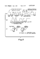
Referring now to FIG. 1, there is shown a general block and pictorial diagram of the apparatus for controlling distributed electrical loads according to the present invention.
The heart of the apparatus for controlling distributed electrical loads is a central controller 50 which automatically controls a user-defined, time-dependent lighting schedule in accordance with a built-in 7-day clock. Operating in a manual mode, controller 50 provides for control of any lighting circuit through its keyboard (not shown in this Figure). For operation in its automatic mode, controller 50 accepts a user defined data base specifying sectors to be controlled (which relays are defined to be in each sector), patterns specifying the states of all relays or any subset of relays, time schedules (when a particular sector or sectors will assume the relay states defined by a particular pattern), switches and condition responsive switchleg inputs (which relays will be activated in response to each particular switch), and condition responsive relationships controlled by analog sensors (a user determines the criteria for analog sensor activation). This data is entered through its keyboard or via mark-sense data cards. Mark-sense data cards carrying scheduling, sector and priority status (including priority erase time), switch, and pattern information are read by a card reader 52 coupled to controller 50. A printer 54 can be coupled to controller 50 to provide a hard copy printout of the user supplied data base, a list of the status of all relays, any priority sector overrides that are in effect and the total number of relays in an "on" state along with the day and time.
Controller 50 is coupled to a plurality of transceiver decoders 56 (labeled 56 (1), 56 (2), . . . 56 (N)) in the figure. The coupling from controller 50 to transceiver decoders 56 is achieved via a data line 58 constituted by a twisted pair of wires. Data line 58 provides a bi-directional communications channel for communication between controller 50 and any of transceiver decoders 56. Associated with each transceiver decoder 56 are a plurality of relays 60 (up to 32 relays) for turning "on" or "off" individual loads 62.
All commands including those resulting from a condition response for changing the state of a relay 60 (and its associated load 62) come from controller 50. However, controller 50 can be requested by a user to initiate a command for changing the status of a particular relay 60 and its associated load 62. Through telephone data sets 64, up to three users can simultaneously access controller 50 via telephones 66. Telephone data sets 64-0, 64-1 and 64-2 provide for interface between controller 50 and the standard public telephone system so that a user can call controller 50 from any location desired. For example, a user could initiate a lighting control function from his home by calling controller 50 through data set 64 before he leaves for the office. Secret codes can be employed to restrict telephone access to authorized persons only.
It is also possible to communicate with controller 50 via transceiver decoders 56. Each transceiver decoder 56 includes provisions for remote switches 68 to be coupled to switchleg inputs thereof. Activation of a remote switch 68, either of the momentary type or maintain type, will cause its associated transceiver decoder 56 to communicate with central controller 50 so as to request a lighting control command to be issued thereby. Sensors having a switch output can be substituted for a manually operable switch (such as switch 68 shown in FIG. 1) to permit a condition responsive override (i.e., fire or smoke detector having a relay output that closes when heat or smoke levels exceed predetermined thresholds).
In addition, analog sensing devices such as a light sensor 70 can be coupled to an analog sensor input section of transceiver decoder 56. These sensors can be polled (interrogated) by controller 50 to provide information related to light levels, heat levels, etc. Based upon the information provided by these analog sensors, controller 50 can issue appropriate commands for altering the status of selected relays. The incorporation of analog sensors and associated information generating capability in transceiver decoders 56 and the use of condition responsive switches coupled to switchleg inputs of the transceiver decoders provide a condition responsive capability for the system.
Controller 50 can be coupled to a non-volatile memory storage system such as a magnetic tape device 72 for storing sector, pattern switch, priority erase time and schedule information. Thus, if controller 50 were to lose power for a substantial period of time, such that all data stored in a volatile form of memory were lost, the data could be easily recovered through the magnetic tape device 72. Means are provided within controller 50 for reading the data stored within magnetic tape device 72.
Because of the micro-cassette tape drives presently available for tape device 72 are not of very high quality for use in digital systems, special clocking techniques are employed. For example, because of the frequency of digital signals read off the micro-cassette will normally vary significantly during the course of a given reading of the tape, special resynchronization self-clocking techniques are utilized to keep a clock circuit synchronized with the data being read from the tape. A continuous weighted average of detected data pulses is used to resynchronize the clock circuit. This results in a continuous lock on the clock frequency with the most recently detected bit frequency being the most effective in controlling the clock frequency. Using this technique, variations of bit frequency approaching 50% in only a single clock cycle may still be successfully read.
Communications Link
As stated, communication between controller 50 and each of transceiver decoders 56 is via a data line 58 formed by a single twisted pair of wires, constituting a bi-directional data communication link or bi-directional communications channel. Both controller 50 and each of transceiver decoders 56 include circuitry for transmitting and circuitry for receiving information. The communication link provides a protocol for the transfer of information to and from these communicating points. The protocol insures that information transmitted and received is free of errors and will not be garbled or interfered with by other communication devices also connected to the data communication link. The communication link, since it can be coupled to different types of synchronized machines each running on an independent clock, is independent of any system timing. The communication link is bi-directional in nature and in one selected mode provides for the utilization of data verification as well as interactive data processing to insure data security while maintaining system throughput.
Arbitration is provided for resolving any bus conflicts arising during simultaneous transmission of two or more control points without garbling, degrading, or interferring with any data being transmitted. The arbitration scheme is suitable for use with the load control system described herein or independently thereof.
As used throughout the description of the communication link, the term "communication point" will be used to refer to any point connected to the data link that has transmitting and/or receiving capability; thus including both controller 50 and all of transceiver decoders 56. The terms "data communication link" and "communication link" include both data line 58 and the protocol in which data is transferred between communication points. The terms "time to compute mode" and "time to compute state" define a time period during which a communication point is not monitoring the communication link. This time is overhead to allow a receiving device sufficient time to process and decode the incoming signal. The term "lockout" is defined to be a mode in which specific communication points are using the communication link in an interactive manner locking out other points from interfering.
The protocol of the communication link defines two possible signal states of the communication link. An active state refers to the state in which the actual information and clock are found during a transmission. As applied to data line 58, the "active" state is defined to be the existence of a voltage potential of 10-30 volts between the two wires of data line 58. The "inactive" state refers to a state wherein the voltage between the two wires of data line 58 is less than 10 volts. The inactive state is of arbitrary duration and is essentially ignored during a transmission sequence. By utilizing a dedicated twisted pair of wires for data line 58, a bus arbitration technique and the data communication protocol, base band signals are transmitted between communication points without the need of extra modulating and demodulating devices. Of course, other communications channels such as power lines, radio channels, etc., could be utilized with appropriate modulating and demodulating devices. The use of an interactive data communication link allows a single communication point to be polled and interrogated without interferring with other communication points. However, other communication points can be actuated asynchronously to use the data line and send information on command from a remote user.
The protocol is based upon a modified form of a standard 1/3, 2/3 pulse-width modulated signaling technique. This modified pulse width modulated signaling technique is hereafter referred to as "modified ratio signaling".
Controller 50 is coupled to a plurality of transceiver decoders 56 via data line 58. Controller 50 is utilized as the command controller that transmits load control information over the data communication link (including data line 58) to the remote transceiver decoders.
Controller 50 is also responsible for normal system maintenance, i.e., the controller interrogates the transceiver decoders in order to verify the state of their relays as well as transceiver decoder operation. This maintenance function is achieved through the same bidirectional communication link between transceiver decoders 56 and the controller 50. At the time when controller 50 is interrogating a particular transceiver decoder 56 for either specifying relay information or checking the status of the transceiver decoder, individual polling is used. Individual polling refers to a transceiver decoder answering a specific question by controller 50 immediately upon receipt of the question. No other transceiver decoder 56 will be allowed to respond to a question directed to a particular transceiver decoder. This condition is defined to be transceiver decoder lock-out as will be further described.
Transceiver decoders 56 are capable of transmitting switch input information from a remote switch 68 coupled to a switchleg input thereof immediately upon its actuation by a user. In this mode, the transceiver decoder 56, to which the remote switch 68 is coupled, responds to a switch input on command of the remote user and does not wait for or require controller 50 to poll for information. This form of data line control is known as asynchronous access of the data communication link. Accessing the data communication link by this method eliminates the need for polling schemes that take much more time and degrade system throughput. The throughput that is realizable by this asynchronous bus access is solely dependent on the current activity on the data link. Therefore, if the data link is not being utilized by another transceiver decoder 56 found on the data bus, the transfer of information from the closure of a remote switch 68 will occur immediately from the particular transceiver decoder 56 to which the switch is connected to controller 50.
In summary, a transceiver decoder 56 will use data line 58 when there is information requested by controller 50 or it will use the data line asynchronously upon a switch input command at its remote control point. Information is transferred in a half duplex form of communication.
The data communication link can couple controller 50 with up to 1,024 transceiver decoders 56. This limitation results from the data bit stream format described hereafter.
Referring now to FIG. 2 there is shown a graphical representation of various hypothetical data waveforms describing the communication protocol. FIG. 2A illustrates that a transmission sequence starts with the data line deemed "free for access or usage". The line free condition is an active (high impedance) state of the line and corresponds to a voltage between the two wires of data line 58 of from 10 to 30 volts. The communication point in need of gaining access of the data communication link sends a long interblock gap (IBG) to grab the line. After the data line has been accessed, a preamble is sent so that the other communication points receiving the data will lock in on the data signal and establish the data rate. The regular IBG follows so that the system may be synchronized thereon. Then the data is transmitted serially as digital information comprising logic level 1's and 0's. Forty bits of information are transmited during the data segment. The forty bits of information correspond to five bytes (eight bits/byte). An IBG follows the data block of forty bits and if more data needs to be sent, another forty bit data stream is sent and if there is no more data, then the line is released.
FIG. 2B shows a data block of forty bits preceded by and followed by an interblock gap. Note that at the end of the final interblock gap, a line free condition exists wherein the line is returned to the active (high impedance) state.
Referring now to FIG. 3 there is shown a flow chart of the transmission sequence utilized by a transceiver decoder 56 to communicate with controller 50. In the "data line free" mode the data line is in a dormant state. It is not being used by any communication point. Protocol to deem the line as being in a free mode as opposed to being accessed is achieved by timing out the inactivity of the data line in the active state for a minimum of three (3) bit periods T. Timeout can be 6-25 msec. depending upon whether phase lock is achieved. With phase lock, timeout can be as short as 6 msec. In the absence of phase lock, timeout automatically occurs at 25 msec. If a signal is to be sent during this time out period for the line free protocol then the previous data rate just received is used to receive the next transmission sequence. It uses the last data rate established and does not expect to see a new preamble. When the line is free it is released for general access and any communication point can attempt to gain control of the line. Therefore, if the state of the data line remains active for a period of time, then the line will be deemed free of data and can be accessed by any communication point.
There are two types of IBG's, one for grabbing the line, and the second for delineation of data blocks within the data stream by an IBG between each block of forty bits of data. In order for a communication point to grab the data line, it accesses the line by forcing an initial IBG (long IBG). The duration of the IBG must be long enough to allow all devices maintained on the line time to set up for receiving the data stream that is to follow. Since the devices on the data line are sequential machines (microcomputers), it is necessary that this duration be a minimum of two msecs. so as to gain the attention of these machines. The duration of the IBG must be long enough so tht any communciation point will have time to compute before the IBG is recognized. The normal IBG is a minimum of three bit periods (3T) of the data rate. The IBG serves as a synchronizing signal to delineate the data blocks being transmitted. When a receiver is out of sync with the transmission, the IBG serves to justify the system and resync a receiver.
The preamble is sent only once during a transmission sequence independent of the number of the data blocks being transmitted. Preamble includes a minimum of four bits at the receiver, a weighted average is taken during each bit period from which the data rate is calculated and its logic threshold determined. The preamble is a sequence of 50 percent duty cycle pulses which a receiver utilizes in order to lock in the data rate (generally 350-4000 bits/second).
A data block includes 40 bits of information using modified ratio signalling for transmitting a series of logic 1's and 0's. The duration and decoding of each received bit is referenced to the previously received preamble. The decoding of the logic levels are not determined by any present condition internal to a receiver. Any number of data blocks separated by IBG's may be transmitted during the time that a communication's point has control of the line.
As stated, the logic levels are transmitted using a modified ratio signalling scheme. The signalling scheme utilizes the active state of the data line for the exchange of information and clock. The duration of the active state during the data block sequence is compared to the previously transmitted preamble which has been stored in memory. This comparison is used to determine the actual logic level being received. Since the data bit input is being referenced to a previous data input, i.e., preamble, it is said to be a ratioed reception. Therefore, common mode distortions caused by parametric shifts in the receiver electronics or in the data line cancel. Since both preamble and data are coupled through data line 58 to a particular control point acting as a receiver, the elimination of parametric variations allow the use of a more simple receiver circuit than might normally be required since tolerances need not be very strict. The logic level thresholds of the received signals are calculated from the preamble.
Modified Ratio Signaling
Referring back to FIG. 2 and specifically to FIG. 2(c), there is shown a signal diagram illustrating the modified ratio signalling scheme and particularly illustrating the effective calculation of the minimum and maximum pulse width value and defining dead bands where no signals are permitted.
The receiver of a communication point has an initial band width of 4-5 Khz for receiving the preamble. After the preamble has been received and data logic thresholds have been calculated, the bandwidth of the receiver is narrowed to reject signals outside of that narrowed bandwidth. This bandwidth narrowing is achieved by a digitally simulated phase locked loop in each transceiver decoder 56, or controller 50. The rejection of signals outside the narrowed bandwidth is achieved by dynamically setting the bandwidth of filters in accordance with the preamble.
Logic levels are defined in terms of the percentage of a total bit period (T) where a bit period is defined to be two (2) times the period of the active state of the 50% duty cycle preamble signal (T50). The duration of the active state as a percentage of the total bit period that determines whether the logic 1 or the logic 0 is present. The preamble is defined to have a bit period of 50 percent of the total clock period (a fifty percent duty cycle signal) and this reference time is used as the basis for making all logic level decisions. As shown in FIG. 2(c), the dead band corresponds to 12.5 percent of the total bit period. The logic "1" and "0" levels are calculated as follows:
The total data bit period (T)=2×T50=100% (i.e, total duration of the active state).
Let the deadband=T50/4=12.5% of the duration of the active state.
Then logic "1" level (threshold determination filtering) is defined by:
T50+deadband≧logic 1≧T-deadband
T50+T50/4≧logic 1≧T-T50/4
62.5%≧logic 1≧87.5%
Similarly, logic "0" level (threshold determination filtering) is defined by:
Deadband=logic 0=T50-deadband
T50/4=logic 0=T50-T50/4
12.5%=logic 0=37.5%
Since the data logic levels are determined only by the active state of the line, the inactive state is ignored and is used to provide a time needed by the microcomputer to compute. This period of the inactive state between bits is constant but cannot exceed two bit periods. Thus, it can not be mistaken for an IBG. A bit period (T) is defined as two active state preamble bits. Of course, regardless of the particular data bit, logic "1" and "0" interpretations are made with respect to the bit period established by the preamble received immediately prior to the data. Information is only carried by the duration of the active state. The inactive state is the time between bits and its minimum duration is determined by the time needed to compute at the communication point acting as a receiver. The inactive state is approximately 160 microseconds in duration. The use of a constant inactive state duration while modulating the active state of the line for the transfer of information provides for a varying bit transfer rate. A logic "0" bit period is approximately 1/3 less in duration than a logic 1 bit period. Therefore, a word transmitted with logic zeros will be transmitted at a higher baud rate than a word with a logic ones. Thus it is possible to communicate with a central point faster that would be possible using a conventional pulse width modulation scheme. Faster throughput is achieved by carrying information only on one state (active) of the data line while making the other state an "I don't care" state. In conventional pulse width schemes, the inactive state period is varied to maintain a fixed clock rate. It takes the same length of time to send eight "1"'s as it does to send eight "0" 's. However, in this system eight "0"'s will be sent faster because the inactive state is not lengthened to maintain a constant clock rate.
Data Line Arbitration
The communication link which is a bi-directional communications channel is able to arbitrate any data line contention without interferring with the current communication sequence. When two or more communication points access the data line for transmission of information there is a bus conflict. This conflict is arbitrated so that there is no loss of information or interference with the current transmission. The arbitration of the data line is achieved either during the line access level or bit transmission level at the communication point. The flow of the arbitration logic is set forth in FIG. 4.
Referring now to FIG. 4 there is shown a flow chart of the data line arbitration protocol. When a communication point has information to be transferred over the data line it must first access data line 58. Data line 58 must be in a free state (high impedence, active state) for the communication point to begin the transmission sequence. If the data line is currently being used by another communication point, the point desiring access automatically holds until the data line is deemed free. During this holding period, the communications point is also receiving whatever data is being sent during the current transmission on the data line. The data held in the communications point needing to be transferred is stored and therefore not lost until the transfer of the information can take place. This stored data can be held indefinitely until the data line has been released and is deemed free for subsequent transmission.
Since the communication points consist of identical electronics and sequential logic, it is possible for two or more transmitting devices to be synchronized with each other. If two devices are synchronized, then they will attempt to access the data line at the same time and not realize that other devices are using it as well. To guard against multiple simultaneous transmissions interferring with the integrity of the data being transferred over the data line, a bit level arbitration scheme has been developed.
The bit level arbitration flow charted in FIG. 4 is achieved by reading the data line on a bit-wise basis after driving the line to a particular state, i.e., the inactive or active state. If there is a discrepancy between the state desired and the actual state of the line as read, then that transmitting device will automatically realize the line is in use and drop off the line into the hold data mode for subsequent transmission when the line is deemed free. The selection of the device driven off the line is achieved dynamically during the course of the transmission sequence and not by a predetermined priority and queing scheme. As two or more communications points transmit, the first bit of information that is different between the two devices will immediately resolve the bus conflict. Since each communication point is uniquely addressable, having its own name, then there is guaranteed to be a sequence of bits during the course of the transmission that will differ. Therefore, there will only be one device left transmitting on the data line at the completion of this transmission sequence. During the arbitration of this information, no data is interferred with or garbled by this data line conflict since it is being achieved on a bit wise level.
The arbitration technique is dependent on the impedance levels of the active and inactive states of the data communications line. The inactive state, is the low impedance state of the line (e.g., the DC resistance of the line in the inactive state is less than 50 ohms). The active state is a higher impedance (e.g., greater than 90 ohms). The impedance of data line 58 is relative to the driver circuit found on the communication point. When there is a conflict between two devices (where one is driving the line to the active state), while the other is driving the line to the inactive state, it is the latter that will win the bus. The device driving the line to the active state is driven off the line since the active state is of higher impedance and, therefore, yields to the low impedance state of the line. Thus, during the bit level arbitration mode, the device that drives the line to the inactive state when the other devices are driving it to the active state, will gain full and uncontested access of the data line.
Performing this arbitration technique dynamically at the time of the actual transmission, provides the utmost in system throughput; i.e., the actual throughput is solely dependent upon the activity of the data communications line at any given time. Furthermore, this also eliminates the need for lengthly polling techniques when information must immediately be transferred and processed upon demand.
The arbitration technique may also be used to freeze or hold the current status of the system without any loss of information. This may be desired during maintenance or downtime procedures. This freezing is achieved by holding the data line in the inactive state for an indefinite period of time so that maintenance procedures can be performed. Since the data line is being held in the inactive state, all information will be held at the communications point and, therefore, not be lost until the information can be effectively transferred.
There is a mode of operation during which controller 50, which is an overriding master device, holds an interactive uninterrupted data conversation with a transceiver decoder 56 (slave). During this interactive interchange of information to a particular transceiver decoder 56, no other transceiver decoder can contest the use of the data line. The other transceiver decoders 56 are said to be locked out and yield the data line to the control of controller 50. This is achieved by defining a master device and slave devices in the system.
The determination of the master/slave relationship of the system components are built into each of the communication points, i.e., controller 50 is the master and the remote transceiver decoders 56 are the slaves. Controller 50 has overriding control of the data communication line such that it can interrupt, stop, or access data line 58 over any of the other slave devices.
The master/slave mode of operation is achieved through the line free determination logic. In this logic the deeming of a line to be free has a different timeout period in masters and slaves. A master device will have a shorter time out period (4 msec.), so that it can slip in and grab the line before a slave device times out (slave time out is 6 msec.). Furthermore, the slave device may become a master upon command of the actual master device. During an interactive conversation between controller 50, a master, and a transceiver decoder 56, a slave, control of data line 58 is automatically transferred to the slave device being accessed. This transfer allows controller 50 to select or poll a specific transceiver decoder 56 without being endangered by a response from an arbitrary device transmitting data.
Therefore, the master device is capable of transferring the control of data line 58 to a specific slave device without any interference.
Transceiver decoder - hardware
Referring now to FIG. 5, there is shown a general block diagram of a transceiver decoder 56. Each transceiver decoder 56 is built around a single chip microcomputer 100, suitably a 3870, which performs all of the logic control functions of the transceiver decoder including the encoding of data from switch and analog sensor inputs for ultimate transmission to the central controller, and the interpretation and execution of instructions from the central controller. The address of each transceiver decoder 56 is jumper-selectable by an address selection bus 102 which sets a 10-bit binary word giving each transceiver decoder an address from "0" to "1023". A switchleg jumper 104 allows the user to select the type of switchleg (momentary or maintain) 68 to be coupled to microcomputer 100 of transceiver decoder 56 through a plurality of switchleg inputs 106. A data input and output circuit 108 couples the data line (data line 58) to microcomputer 100. Data input and output circuit 108 includes optoisolators for providing an isolated differential data input and output for enhancing noise immunity against electromagnetically coupled noise sources. As previously stated, the data communications link is bi-directional. An analog sensor section 110 allows the coupling to a transceiver decoder 56 of up to eight analog sensors (temperature, light sensors, snow, ice, humidity, wind, smoke, etc.) using an 8-channel analog multiplexer and a dua-slope A/D converter. The analog sensors are of the variable impedance type and are represented by transducer 112 in the Figure (analogous to light sensor 70 shown in FIG. 1). These analog sensors can be polled by controller 50 and in response to such polling, send data via their associated transceiver decoder 56 through data line 58 to the controller providing information related to ambient lights, temperature conditions, etc. for initiating an appropriate response to such conditions.
The use of analog sensors and switches renders the system "condition responsive". The time dependent scheduling of relays of selected sectors responding to a pattern of relay states illustrates the use of time as a condition. However, the system can also be condition responsive through its switchleg inputs and analog sensor inputs. Analog sensor section 110 (see FIG. 5) provides connection for up to eight (8) analog sensors, i.e., devices providing a range of impedances or voltages responsive to ambient conditions such as light level, temperature, humidity, etc. Controller 50 can poll (interrogate) these sensors periodically and issue programmed commands in response to their status. There are also available on the commercial market switch type sensors. Such sensors detect thresholds of temperature, light, humidity, etc. and close switch contacts when their predetermined threshold is exceeded. These switch type sensors can be treated as substitutes for switches 68 coupled to the switchleg inputs of a transceiver decoder 56. The response to the actuation of a switchleg is defined by the user regardless of the particular device utilized to close the contacts of the switchleg. Thus a smoke detector having a switch-type output can be coupled to a switchleg of a transceiver decoder 56 and programmed to activate a specific lighting pattern for an emergency sector.
Watchdog reset circuit 120 provides reset and preset capability for transceiver decoder 56. When microcomputer 100 is operating normally, i.e., sequencing through its instructions beginning at its base (zero) address and proper sequence of instructions it sends a STROBE signal to watchdog reset circuit 120. Whenever the STROBE signal ceases, watchdog reset 120 senses that microcomputer 100 is malfunctioning. Either it has lost a bit and is executing an improper instruction or it has locked into a loop and is not following its proper sequence of instructions. Watchdog reset circuit 120, in response, sends a RESET signal to microcomputer 100 forcing it back to its zero address to begin its instruction sequence again. Watchdog reset circuit 120 also includes a preset switch for giving a user the ability to override a transceiver decoder 56 by turning on all relays. The present switch would be utilized in the event of a data line 58 or controller 50 failure and permits circuit breaker control of all relays without the present necessity of hard wiring changes.
Microcomputer 100 is clocked by an external clock crystal 114.
Commands to specific loads issue from microcomputer 100 through drive matrix lines 124 and are coupled to a bank of relay drivers 126 for activating individual relays associated one with each specific load.
The general block diagram shown in FIG. 1 shows several transceiver decoders 56 coupled along data line 58 serving as the bi-directional data link. Transceiver decoders 56 are individually addressable and are utilized to directly control relays specified on command of controller 50.
The system is a closed loop wherein controller 50 can interrogate the status of the remote transceiver decoder 56. This status information can be the current relay pattern in force such that justification of system activity can be made and verified. A command from controller 50 can either initiate load actuation or be in a resonsive mode for interrogation and self-diagnosis. Data sent to controller 50 from a transceiver decode 56 can either be in response to an interrogation command from the controller or it can be asynchronously sent in response to a remote user input, such as the activation of a switchleg by a switch 68 or a condition responsive device coupled to a switchleg input. Since there is no critical system timing, a user can actuate an input to a transceiver decoder 56 at any time. When an input is recognized, the appropriate information is transmitted to controller 50 which in turn decodes the switchleg signal and sends the appropriate command to actuate the proper relays and loads.
The transfer of data between controller 56 and a transceiver decoder 56 is achieved over data line 58. Data is transmitted in a serial fashion as described in great detail above.
Data Stream Format
Referring to FIG. 6, there is shown a diagrammatic representation of the format of the data stream. FIG. 6(a) shows a transmission block of 40-bits (5-bytes) including multiple fields. The data stream includes a function word, an address word, a data field zero, a data field 1, and an error check work. A word refers to one byte of 8 bits of binary information.
The first byte of the 40-bit data stream is the function word. Three bits called F0, F1 and F2, shown in FIG. 6(a), comprise the binary pattern that is used to dynamically set the type of transmission sequence. Since the decoding of this function word is critical to the accurate transfer of data, it is complementary-redundant bit-wise error-checked. The error checking for the function bits is in the three bits following F0, F1 and F2 called F0, F1 and F2. Before the data is decoded, the function words are error-checked for accuracy. These six bits are exclusively OR'ed together in the appropriate bit positions such that valid data exist when they differ in logic level in each bit position. This will produce a logic one in the exclusively OR'ed section indicating that data is valid.
The function word is present in all data transfers between the controller 50 and a transceiver decoder 56. The three bits provided in the function word provide a binary number from 0 through 7 which indicates one of eight possible modes. Modes 0 through 4 indicate that the data stream was transmitted by controller 50. Modes 5 through 7 indicate that the transmission emanated from a remote transceiver decoder 56. Table 1 summarizes the different modes specified in the function word. In general, the function word specifies the type of data being transferred and the data security which affects the system throughput.
              TABLE 1                                                     
______________________________________                                    
FUNCTION WORD - TRANSMITTED BY CENTRAL                                    
CONTROLLER                                                                
F.sub.2                                                                   
     F.sub.1                                                              
            F.sub.0                                                       
______________________________________                                    
0    0      0      Mode 0  Install Specified                              
                           Relay States in  Data                           
                           Fields  0 and 1                                 
0    0      1      Mode 1  First Transmission of Relay                    
                           States in  Data Fields  0                        
                           and 1                                          
0    1      0      Mode 2  Second Transmission of                         
                           Complementary Relay States                     
                           in Mode 1                                      
0    1      1      Mode 3  Interactive Data Verifi-                       
                           cation                                         
1    0      0      Mode 4  Data Interrogation Mode-                       
                           Use (Auxiliary Function                        
                           Word in Data Field 0)                          
______________________________________                                    
FUNCTION WORD - TRANSMITTED BY TRANSCEIVER                                
DECODER 56                                                                
F.sub.2                                                                   
     F.sub.1                                                              
            F.sub.0                                                       
______________________________________                                    
1    0      1      Mode 5  Current Relay States in                        
                            Data Fields  0 and 1                            
1    1      0      Mode 6  Remote User Activated                          
                           Switchleg                                      
1    1      1      Mode 7  Data Type Found in Data                        
                           Field 0                                        
                           Analog Sensor Data                             
                           Transceiver Decoder 56                         
                           Status for Testing                             
                           (Secondary Auxiliary Function                  
                           Word in Data Field 0)                          
______________________________________                                    
Continuing to refer to FIG. 6(a), the address of the transceiver decoder 56 includes 10 binary bits which provide 1024 unique addresses that exist on a single data communication line. The high order address bits, A8 and A9, exist in the least two significant bits of the function word. The remaining address bits, A0 to A7, are contained in the second byte of the transmission block, the address word.
The type of data that is contained in data field 0, which is the third byte of the transmission block, is specified in the function word. For modes 0 to 3, data fields 0 and 1 contain the appropriate loading pattern for 16 relays specified by controller 50. In mode 4 (see Table 1) data field 0 contains an auxiliary function word which is decoded similarly to the function word of the first transmission byte. Each auxiliary function word includes a lower and upper order nibble of 4 bits each. The lower order nibble of the auxiliary function word, (see FIG. 6(b)), f0-f3, specifies the particular flag which must be decoded. The higher order nibble, f0-f3, consists of the complementary redundant bits of the auxiliary function word which is used for error checking. These bits are exclusively OR'ed with the auxiliary flag to determine their validity. Table 2 is a summary of the auxiliary function words.
              TABLE 2                                                     
______________________________________                                    
 AUXILIARY FUNCTION WORD TABLE FOR MODE 4                                 
(Decoded in Data Field 0 Transmitted by                                   
Central Controller)                                                       
f.sub.3                                                                   
     f.sub.2                                                              
            f.sub.1                                                       
                   f.sub.0                                                
______________________________________                                    
0    0      0      0       Individual relay override,                     
                           force to OPEN state. Relay                     
                           number in data field 1.                        
0    0      0      1       Individual relay override,                     
                           force to CLOSE state.                          
0    0      1      0       Acknowledge of valid loading                   
                           pattern - Mode 3 response                      
                           (See Table 1)                                  
0    0      1      1       Negative acknowledge indica-                   
                           tion of erroneous relay                        
                           pattern data, Mode 3 response.                 
0    1      0      0       Interrogate current status of                  
                           relays. NOTE - Does not over-                  
                           ride pending switchleg                         
                           request.                                       
0    1      0      1       Reserved for future use.                       
0    1      1      0       Interrogate system status used                 
                           in debugging. Does not over-                   
                           ride pending switchleg                         
                           request.                                       
0    1      1      1       Reserved for future use.                       
1    0      0      0       Request for analog sensor                      
                           reading whose sensor address is                
                           in data field 1.                               
1    0      0      1       Interrogate relay status-                      
                           overrides any pending                          
                           switchleg request.                             
1    0      1      0       Interrogate current system                     
                           status - override any pending                  
                           switchleg request.                             
1    0      1      1                                                      
1    1      1      1       Not Used.                                      
______________________________________                                    
Modes 5 and 6 (see Table 1) are transmitted by tranceiver decoder 56. Data fields 0 and 1 contain either the current state of the relays or the activated switchlegs by the remote user.
Referring now to FIG. 6(c) mode 7 is also sent by the transceiver decoder 56 and indicates, in the high order nibble of data field 0, a second set of auxiliary function words sf0 and sf1 specifying the type of data found in data field 1 and in the low order nibble of data field 0. This second auxiliary function word is used to send the analog sensor reading as well as information used in testing the transceiver decoder 56. Table 3 summarizes this second auxiliary function word.
              TABLE 3                                                     
______________________________________                                    
SECOND AUXILIARY FUNCTION WORD                                            
sf.sub.1 sf.sub.0                                                         
______________________________________                                    
0        1       System status contained in low                           
                 nibble of data field 0 and in data                       
                 field 1.                                                 
1        0       Analog Data enclosed in data field                       
                 1 - addressed in low nibble of data                      
                 field 0.                                                 
______________________________________                                    
The fifth and last byte of the transmission block (see FIG. 6(a)) is the parity error check word. This generates even parity for every four bits of data of the previous four bytes of the transmission block. Before any action is taken by transceiver decoder 56, a parity check on the previous bytes is performed with the error check word to determine the validity of the transmission block. If an error is detected, no action will occur and the transceiver decoder will continue its normal activity and wait for a new command from the controller 50, or remote user input.
Mode 0 is the binary bit pattern 000 shown in Table 1. This is the fastest mode providing the highest degree of system throughput. This mode, sent by the controller 50, informs a transceiver decoder 56 that load control data is contained in data fields 0 and 1. Transceiver decoder 56, upon receipt of this data block, performs an address and error check using the error check word and immediately installs the specified states of relays 60.
Modes 1 and 2 provide a higher level of data security at a reduced system throughput than mode 0. Mode 1 indicates to transceiver decoder 56 that load control information is contained in data fields 0 and 1, as in mode 0. However, no action occurs until after a second transmission, mode 2, which must follow immediately. The mode 2 transmission consists of complementary redundant load control information in data fields 0 and 1. After the reception of mode 2, data fields 0 and 1 of mode 1 and mode 2 are exclusively OR'ed together to insure that each appropriate bit position differs in logic level indicating valid data before actuation occurs. If the transmission is made out of sequence, that is, mode 2 before mode 1, or if the data field bits agree in logic level, then an error condition is said to exist and no action by the transceiver decoder will take place.
Mode 3 is an interactive sequence of data transfer to and from transceiver decoder 56. It provides the highest degree of data security at the slowest system throughput. The sequence of events in this communication scheme are in the following order.
a. Controller 50 specifies load control information in data fields 0 and 1 as in mode 0.
b. Transceiver decoder 56 performs an address and error check on this transmission block and immediately responds by transmitting the load control information from data fields 0 and 1 back to controller 50.
c. Controller 50, upon receipt of this data, verifies that the loading pattern is correct and then immediately transmits a positive acknowledge so that load actuation can take place. If controller 50 receives conflicting load control data, it will issue a negative acknowledge signal indicating to transceiver decoder 56 to abort the transmission sequence.
d. Transceiver decoder 56, upon receiving a positive acknowledgement, will then install the specified loading pattern. If at any time the transmission of this information is out of sequence or a negative acknowledgement is received, transceiver decoder 56 will abort this operation.
Mode 4 specifies a particular task to be performed which may require a response by the transceiver decoder 56 to controller 50. The mode 4 task is described in Table 2 and is specified in data field 0.
The state of an individual relay can be modified by controller 50 without affecting the other loads connected to a transceiver decoder 56. Controller 50 can also request a reading of an analog sensor whose address appears in data field 1. Controller 50 can interrogate the status of the loads controlled by transceiver decoder 56.
Mode 5 is transmitted by transceiver decoder 56 and contains the current state of the relays in force in response to a read request from controller 50.
In mode 6, the state of an activated switchleg is transmitted to controller 50 by transceiver decoder 56. A switchleg 68 is activated by a user and indicates whether the position is on or off.
Mode 7 contains status information requested by controller 50. Transceiver decoder 56 responds in this mode for the following two cases:
a. Analog Sensor Reading
An analog sensor (such as transducer 112 shown in FIG. 5) whose address is in the low order nibble of data field 0 is supplied in data field 1. This is only sent back to controller 50 after it has requested the analog sensor reading.
b. System Inquiry Mode
This mode is used for testing and debugging transceiver decoder 56. When controller 50 asks for system status, the low order nibble of data field 0 will contain the condition of several user selectable jumpers. Data field 1 will contain the value of the data rate counter used in determining the logic level inputs from data line.
Up to eight switches 68 can be connected to switchleg input circuit 106 of transceiver decoder 56 providing programmable remote user inputs to controller 50. Switches 68 can be either maintain or momentary type. The type of switchleg is determined at the time of installation by a jumper selection at switchleg jumper 104 (see FIG. 5). When momentary switches are selected, transceiver decoder 56 will only transmit data indicating the state or direction of the contact when there is a MAKE condition or on positive action only. For the maintain switches, transmission to controller 50 will occur on a MAKE or BREAK condition, i.e., whenever the switchleg changes state. Switchleg actuation is achieved asynchronously and independently of any activity of controller 50 and other transceiver decoder 56 connected with data line 58. This independence allows each transceiver decoder 56 to function without any critical system timing and thereby reduces system complexity and its susceptibility to erroneous action while increasing system throughput. Activation of a switchleg input by the closure of a switch 68 asynchronously causes a signal to be sent to controller 50 requesting an override instruction for a particular relay 60 and its associated load. If controller 50 has been programmed to respond to the activation of switch 68, a command will be sent to the transceiver decoder 56 associated with the relay requiring activation.
Transceiver decoder 56 contains filtering and debouncing logic for eliminating multiple switchleg actuations and for rejecting errors caused by noise. Switchleg inputs are read at 80 msec intervals and require that the user enable a switch for at least 100 msec to guarantee a true reading.
When a switch 68 is activated by a remote user, a switchleg output word is formed in data fields 0 and 1 of a transmitter buffer in transceiver decoder 56. The switchleg word is then transmitted to controller 50 as soon as the data line is deemed free. Data field 0 will contain the particular switchlegs that have been activated and data field 1 contain the desired state. The bit positions that are set in data field 0 indicate which switchlegs were activated by the remote user. The corresponding bit positions in data field 1 indicate the state of the activated switch 68 (on or off). For example, referring to FIGS. 6(d) and 6(e), if switchleg 6 has been activated, then data bit 6 will contain a 1 in data fields 0 and the corresponding bit position in data field 1 will contain the state of the switchleg (logic 1 for on and logic 0 for off).
If data line 58 is in use, transceiver decoder 56 will standby, latching the switchleg request until the information can be sent. Therefore, the switchleg actuation is not lost and does not require multiple actuations by the user. If while transceiver decoder 56 is standing by another switchleg is activated or if multiple switchleg inputs occur at the same time or if the same switchleg is reactivated, then all the inputs will be added to the current switchleg output word waiting to be sent to controller 50. All inputs are latched and provide "N-key rollover" insuring accurate readings even if multiple switches are simultaneously actuated. This will guarantee that no data is lost due to the interaction of the other devices.
The transmission of the switchleg data occurs asynchronously with controller 50. This eliminates the need for slow polling methods. The throughput is therefore a function of the current activity on the data bus.
FIGS. 7-17 detail the specific circuitry and logic functions performed by transceiver decoder 56. The heart of each transceiver decoder 56 is a 3870 single chip microcomputer 100 which contains a 2K ROM program providing all required logic functions.
Transceiver Decoder Microcomputer-Connections
Microcomputer 100 is a general purpose microcomputer that is transformed into a special purpose microcomputer by its particular program burned into read only memory (ROM). All logic functions of transceiver decoder 56 are carried out by microcomputer 100. Signal or pin names as used throughout this specification can be correlated to those shown on FIG. 7.
Referring now to FIG. 7, there is shown a detailed signal and pin assignment for microcomputer 100. The address bus includes pins 3-6, 19-16 and 33-32, respectively. Serial input data from data line 58 is coupled into SID on pin 38. Serial output data to data line 58 is coupled from SOD pin 26. The digital signal representing the status of the analog sensors coupled to analog sensor section 110 (see FIG. 6) is coupled into ANINP pin 27. Selection of particular banks of relay drivers is made by signals on a relay bank selection bus including RESEL0 . . . RESEL7 at pins 8-15 respectively. Particular relay drivers within each bank are selected by MD0-MD7 at pins 37-34 and 22-25 respectively. Switchleg inputs 106 are multiplexed onto the MD0-MD7 lines.
Referring now to FIG. 8, there is shown a schematic diagram of data input and output circuit 108.
Transceiver Decoder Data I/O
Data input and output circuit 108 provides isolation between data line 58 and microcomputer 100. Specifically, isolation from data line 58 to input SID (pin 38 of microcomputer 100) is provided by an optoisolator 150. Isolation from the data output SOD (pin 26 of microcomputer 100) to data line 58 is provided by a second optoisolator 152. All circuitry from the data line side of optoisolators 150 and 152 to data line 58 are powered by an isolated power supply providing voltages +P and -P.
Data is coupled to and from data input and output circuit 108 via a fusible link 154. A high impedance is provided to the data line by a series resistor 160 in the data path. A small amount of filtering is provided by a capacitor 158 across the data line. Only minimal filtering is required because the primary filtering is handled by digital signal processing techniques within microcomputer 100. A zener diode 162 establishes a 10 volt threshold level for decoding the logic levels of received data. This threshold provides a certain measure of noise immunity.
The normal state of data line 58 is active (high impedance) when the line is free. This corresponds to a voltage level of greater than 10 volts between the two wires of the twisted pair forming data line 58 in accordance with the definition of the active state and the detailed discussion of the communication link.
A voltage of greater than 10 volts at data line 58 effectively turns on transistor 164 which turns off transistor 166 and maintains optoisolator 150 in an off condition. Since the normal condition is low power, there is very little stress on optoisolator 150, enhancing system reliability. When optoisolator 150 is off, the collector of transistor 170 is pulled up to five volts by a resistor 173 coupled thereto. Because amplifier 172 is an inverting amplifier, a logic level zero will appear at the data input SID for coupling into pin 38 of microcomputer 100. In summary, the normal, active state of the data line (data line 58) impresses a logic level zero on the SID input of microcomputer 100.
When data line 58 is driven by controller 50 or another transceiver decoder 56 to a voltage level of less than 10 volts between the wires of the twisted pair, zener diode 162 blocks current to transistor 164 causing it to be in the cut off state. Transistor 164 then turns on transistor 166 which causes optoisolator 150 to turn on (current through diode 168). The turning on of optoisolator 150 causes transistor 170 to turn on thereby establishing a zero level at the input of amplifier 172 and a logic level one to appear at the data input SID of microcomputer 100. Thus, when the data line is driven to an active state (low impedance) a logic level "1" will appear at the data input SID of microcomputer 100.
When microcomputer 100 of a transceiver decoder 56 wants to drive the data line (data line 58) it must bring the data line to an inactive (low impedance) state. No transceiver decoder 56 is capable of sourcing current onto the line, but rather drives the data line 58 to a lower impedance state thereby impressing a signal upon it. Only controller 50 sources current onto data line 58. There are two states defined for the data line: a high impedance state (greater than 90 ohms) wherein the voltage level between the wires of data line 58 exceeds 10 volts and a low impedance state (less than 50 ohms) wherein the voltage level between the wires of the twisted pair is less than 10 volts. This impedance level difference allows the use of bus arbitration. In order to drive the data line, a transceiver decoder 56 must drive the data line to a low impedance condition. A logic level "0" appearing at the output data line SOD of microcomputer 100 will turn on an LED 174 within optoisolator 152. Optoisolator 152 includes a photo-transistor 176 which is turned on by the conduction of LED 174 thereby supplying curent from the isolated power supply to the output drive transistor 178. Turning on transistor 178 across the data line sinks enough current so that the voltage level between the wires of data line 58 falls to less than 10 volts and the impedance between the wires drops below 50 ohms. Current is sunk through fusable link 154. If transistor 178 fails so as to present a low impedance between its collector and emitter, data line 58 is effectively shorted. By virtue of data line 58 being held in a low impedance state for an abnormal length of time, controller 50 detects a malfunction and responds by sending a pulse of approximately one amp down data line 58. This pulse is designed to blow fusable link 154 of the malfunctioned transceiver decoder 56 thereby severing that particular transceiver decoder from data line 58. This detection and subsequent response by attempting to blow fusible link 154 on a malfunctioning transceiver decoder 56 constitutes the self clearing mode of the transceiver decoder operation.
As stated, optoisolators 150 and 152 and an isolated power supply provide isolation between microcomputer 100 and the data line. This isolation helps to maintain the integrity of data line 58 and provides noise immunity. Data line 58 runs throughout the entire system and is quite long. It is possible for noise to be coupled into data line 58 from various electrical sources. Even if the line were brought to a level of 1,000 volts with respect to earth ground, isolation prevents this higher voltage level on data line 58 from affecting either controller 50 or microcomputer 100. Both controller 50 and microcomputer 100 will still be able to distinguish active and inactive data levels by sensing the differential voltage between the wires of data line 58.
By using a twisted pair for data line 58, common mode rejection is enhanced. A property of twisted pair is that in the presence of a strong magnetic field, signals coupled into one wire of the twisted pair will also be coupled into the other wire. Common mode noise is therefore rejected on input and output circuit 108 and only the differential signal between the wires of data line 58 is amplified and decoded. If one wire of the twisted pair of data line 58 were referenced to ground, this would not be possible.
Analog Sensor Section
Referring now to FIG. 9 there is shown a more detailed diagram of analog sensor section 110 of a transceiver decoder 56. Analog sensor section 110 accommodates up to eight analog inputs for coupling to analog devices such as photocells and thermistors. These analog inputs are periodically interrogated by controller 50 to determine the ambient conditions that exist at a remote control point. Light and temperature levels can be read by connecting the appropriate sensors to analog sensor section 110.
One of eight analog inputs is selected by a multiplexer 200 having sensor select inputs multiplexed onto the MO0, MD1, and MD2 outputs (pins 37, 36, and 35) of microcomputer 100. Utilizing these three sensor select bits, multiplexer 200 is able to select one of eight sensor input circuits 202. A representative sensor input circuit 202 is shown coupled to the AI0 input of multiplexer 200. The output of multiplexer 200 is coupled through an isolation amplifier 204, suitably a voltage follower circuit utilizing an operational amplifier, to an analog to digital converter 206. Analog to digital converter 206 is suitable a dual slope A/D converter having a maximum conversion cycle time of 22 milliseconds. The output of analog to digital converter 206 is coupled to the ANINP input (pin 27) of microcomputer 100. Ramp control of analog to digital converter 206 is coupled to the ANCNTL output (pin 28) of microcomputer 100.
Watchdog Reset
Referring now to FIG. 10 there is shown a detailed schematic diagram of Watchdog reset circuit 120. Because transceiver decoder 56 is based upon a single chip microcomputer 100, it operates as a sequential machine executing a sequence of instructions. In its normal power-up mode, the microcomputer must periodically reset itself in order to justify its operation back to its zero address. In addition, the sequence of instructions to be executed depends upon values stored within internal registers such as its program counter. Due to the presence of noise, it is possible for internal registers to drop a bit of data in such a manner that the data bit loss would assure microcomputer 100 to execute an improper instruction, an out of sequence instruction, or execute on data rather than the appropriate instruction. It is possible for microcomputer 100 to be forced into an operating loop which effectively latches the entire board and prevents it from responding to any command from external sources. In addition, it is advantageous to provide the capability to override the system at a transceiver decoder 56 in the event of a controller 50 or data line 58 failure.
Watchdog reset circuit 120 provides a source of periodic reset pulses for justifying the operation of microcomputer 100 to its zero address for the start of each of its normal cycles through its address sequence. In addition, watchdog reset circuit 120 provides reset pulses to justify microcomputer 100 after a dropped data bit has caused it to stray from its normal sequence of operation. In addition, an emergency override switch 221 provides a preset signal for causing all relays to be turned on regardless of signals on data line 58. Operating in such a preset mode effectively returns all relays associated with the preset transceiver decoder 56 to circuit breaker control.
In the absence of a STROBE signal from microcomputer 100, watchdog reset circuit 120 provides RESET pulses to the microcomputer every 240 milliseconds. Thus, in the absence of a STROBE pulse from microcomputer 100, the microcomputer would be returned to its zero address every 240 milliseconds when a pulse is received at its reset input. The time period between reset pulses is controlled by the RC time constant associated with a resistor 224 and a capacitor 226. When allowed to charge, in the absence of a STROBE pulse, capacitor 226 charges through resistor 224 to a predetermined voltage level, typically 2.5 volts. When capacitor 226 is permitted to charge, it trips a Schmitt trigger 227 having an inverting output coupled to the reset input line of microcomputer 100. Once activated by a RESET signal, microcomputer 100 executes the instruction at its zero address location as if it were being powered up for the first time.
When microcomputer 100 is functioning normally and executing its instructions in proper sequence, it clears the charge from capacitor 226 by coupling a STROBE signal through inverting amplifiers 220 and 222 to capacitor 226. When microcomputer 100 is operating properly, a STROBE of approximately 4 microseconds appears every 25 milliseconds. These STROBE pulses, 25 milliseconds apart, clear the voltage from capacitor 226 before Schmitt trigger 227 can be triggered, thus inhibiting RESET pulses from watchdog reset circuit in the absence of STROBE pulses from microcomputer 100, a feedback loop formed by a diode 230 and resistor 232 cause a periodic pulse signal to appear on the RESET line. In essence, the STROBE can be thought of as the heart beat of microcomputer 100. Until that heart beat is sensed, the RESET line will continue to pulse the microprocessor until the computer is operating properly and the STROBE is found.
When controller 50 fails or data line 58 is severed, no data can be transferred to the relays associated with a transceiver decoder 56. Therefore means are provided for overriding data line control of relays. The activation of preset switch 221 provides a signal forcing all relays on thereby returning them to circuit breaker control without the necessity for hard wiring them around a transceiver decoder 56. This provides an emergency backup for a controller 50 or data line 58 failure.
Preset switch 221, when activated, provides a pulse on the RESET line. When microcomputer 100 senses a RESET pulse, it reads the PRESET input line. The PRESET input line is coupled through inverter 234 to preset switch 221. The activation of switch 221 effectively grounds the input of inverter 234 thereby providing a logic level 1 at its output. That logic level 1 at the output of inverter 234 appears on the preset line simultaneously with the appearance of a RESET pulse on the reset line. Switch 221 is AC coupled by a capacitor 228 to the RESET line. AC coupling insures that the RESET line will pulse while the PRESET line stays at DC. This insures that when microcomputer 100 responds to a reset pulse, it will read the PRESET as being at a logic level 1 and know that it should go into a PRESET state and force all relays on.
Switchleg Input
Referring now to FIG. 11, there is shown a detailed schematic diagram of switchleg input circuit 106 and switchleg jumper circuit 104. Each transceiver decoder 56 includes switchleg inputs for up to eight remote switches 68. By the coupling or decoupling of a switchleg jumper 250, switchleg jumper circuit 104 appropriately instructs microcomputer 100 so that either momentary or maintained type switches can be used. There are 16 inputs labeled 1-red . . . 8-red, 1-black . . . 8-black. Each of the red inputs is coupled through a resistor 252-0 . . . 252-7 to one input of a NAND gate 254-0 . . . 254-7 respectively. The outputs of NAND gates 254 are coupled respectively to the MD0 . . . MD7 input lines of microcomputer 100. The other inputs of NAND gates 254 are tied together and coupled to the CCSEL #2 input of microcomputer 100. Similarly, the eight black switch inputs are respectively coupled through resistors 256-0 . . . 256-7 to one input each of NAND gates 258-0 . . . 258-7 respectively. The respective output lines of NAND gates 258 are also coupled to the MD0 . . . MD7 inputs of microcomputer 100. The second inputs of NAND gates 258 are tied together and are coupled to the CCTYPE/CCSEL #1 input of microcomputer 100. The output of switchleg jumper circuit 104 is also coupled to the CCTYPE/CCSEL #1 input of microcomputer 100.
The switchleg voltage VSL is 20-40 volts generated in a switchleg power supply (not shown). The combination of resistors 266 and 268 coupled into each of gates 254 and 258 provide appropriate voltage levels to operate the gates so as to provide a 3.5-5 volt output for coupling into standard TTL logic entering microcomputer 100. When jumper 250 is removed from jumper circuit 104, the input of an amplifier 262 is pulled up to a 5 volt level by the action of a resistor 264 in series with a diode. This forces the inverted output of amplifier 262 and the connected CCTYPE/CCSEL #1 input at pin 29 of microcomputer 100 to a logic level 0. With pin 29 of microcomputer 100 at a logic zero, switchleg input circuit 106 is set for the use of maintain switches, that is switches which maintain contact between their poles rather than making a momentary contact and returning to an open normal condition immediately thereafter. By forcing pin 29 of microcomputer 100 to a saturated logic level zero state, it is impossible to drive that input line high and thus, one input to each of gates 258 will be a logic level zero disabling gates 258 since they are not used with maintain switches.
The maintain mode switches will be coupled to the eight red inputs coupled to gates 254. Again, a maintain mode switch maintains contact closure until the contact is opened. Using maintain mode switches, coupled to the eight red inputs, if a switch is open, the red input line is pulled up to switchleg voltage VSL which is between 20 and 40 volts depending upon voltage variations and loading. A voltage of 20-40 volts is utilized so that there will be sufficient voltage to prevent the mechanical contacts of the switches from building up an oxide layer thereby rendering the switch unreliable. Also, the use of a voltage between 20 and 40 volts, as opposed to using logic level voltage, allows the switchleg to be somewhat remote from the transceiver decoder 56. With the IR loses associated in long wires, a logic level signal would require that the switches be only a short distance from transceiver decoder 56. With voltage VSL applied, the switchleg voltages are divided through resistors 266, 252 and 268. This voltage division provides a standard TTL logic level of 3.5-5 volts.
In order to utilize momentary type switches, jumper 250 is inserted in switchleg jumper circuit 104 thereby forcing the output of amplifier 262 to a logic level 1. Thus, gates 258-0 . . . 258-7 become operable and momentary type switches or contact closures can be coupled between the corresponding red and black inputs for a particular switch member.
Microcomputer 100 at intervals of from 75 to 80 milliseconds reads (polls) the switchlegs connected to its MD0-MD7 inputs at its pins 37-25 respectively. This reading operation is done without any command from any other devices connected to its data lines. This reading is under the logic control of microcomputer 100. It is done independently and on its own, and in accordance with its internal clock. Essentially, microcomputer 100 is a sequential machine which operates through its various states to do specific tasks. Even though it is continuously interrogating the switchlegs to determine their status, it is not continuously sending that data back to controller 50. The only time a switchleg 68 requires action is when there is a change in its state. That is, when its state is different from the previous reading of it 75 to 80 milliseconds before. For example, assuming a switch 68 is coupled to switchleg input 1, the input of NAND gate 254-0 will be allowed to pull up to a plus voltage thereby enabling the gate. When a switchleg is interrogated or polled by microcomputer 100, a high voltage appears on the output of gate 254. A TTL gate is used where output is of the open collector variety. It will either saturate and stick the line at a logic zero or be in a high impedance state. Therefore, the driving of the line to a logic level 1 is performed on internal pull-up devices or in this case by resistors located internal to the microcomputer 100.
Once a transition has been made from an open switch state to a closed switch state or from a closed switch state to an open switch state a change in disposition of the switch from the prior reading about 80 milliseconds ago takes place. A series of readings then follows in order to prevent an erroneous reading. To guard against erroneous readings, 10 readings are successively made and they must all have the same reading for a switch to be accepted as a closure or as a change of state. Once the change of state has been verified, the microcomputer 100 will attempt to access the data line in order to transmit this information to controller 50.
In the case of a momentary type switch only the positive action of temporarily closing the switch is meaningful. Contact is made and then broken. However the breaking of contact is not acted upon. Momentary type switch connections can be used for photo relays and other types of condition responsive devices having a switch-like trigger mechanism coupled to a switchleg input as well as for momentary type switches. By using momentary type switches you can connect the off stage of the switch to different switch numbers to provide increased flexibility for the system.
Relay Drivers
Referring now to FIG. 12 there is shown a detailed schematic diagram of relay drivers 126 coupled to their drive matrix lines 124. Transceiver decoder 56 includes a bank of 32 relay drivers organized into an upper bank of 16 relay drivers and a lower bank of 16 relay drivers. Each relay is associated with two gates 300 and two amplifier drivers 302. In the upper bank the gates are numbered 300-1 . . . 300-16 and the inverting amplifiers are numbered 302-1 . . . 302-16. In the lower bank the gates are numbered 300-17 . . . 300-32 and the amplifier drivers are numbered 302-17 . . . 302-32. In both the upper and lower banks, the gate/amplifier combinations are wired in groups of eight (to control four relays) with one gate input commonly connected. Pins 8-15 of microcomputer 100 are relay bank select signals RLSEL0 . . . RLSEL7 respectively and are coupled to the common input of each group of gates/amplifiers. Data bus lines MD0 . . . MD7 on pins 37-25 of microcomputer 100 are connected one each to each of the gates/amplifiers of each group. Thus, a particular relay bank select signal coupled with a specific address line defines only one relay including two gates 300 and two amplifier drivers 302. When using all 32 relays, transceiver decoder 56 is assigned two consecutive addresses, the first being an even address and the second being the odd address immediately following the even address.
Microcomputer 100 responds to the even and odd address coding wherein the least significant figure is in essence a "don't care" bit. The particular transceiver decoder 56 addressed will respond to either of these addresses. The upper bank of relay drivers will respond to the even address and the lower bank of relay drivers will respond to the odd address. Each of amplifier drivers 302 includes a Darlington pair (open collector) of transistors for directly driving a relay. It further includes a transient protection diode to protect from inductive load kick-back from a relay that has been triggered. The relays are standard latching type relays having three wires, one red and one black and one blue. The red and black wires of the relay connect to a pair of adjacent amplifier drivers 302. A pulse on the black wire forces the relay into an open state and a pulse on the red wire forces the relay into a closed state. The blue wire is the common and is coupled to a power supply. To drive the relay to either of its bistable states (open or closed) the red or black wire is grounded by an enabling pulse from amplifier driver 302.
As stated, each group of four relays is coupled to a relay bank select signal (one of pins 8-15 of microcomputer 100). Enabling a given bank select signal enables up to four relays. However, due to excessive loading on the semiconductors in the relay drivers, only two relays in a bank are activated at the same time. Data appearing on data lines MD0 . . . MD7 specify the particular state for each relay winding when a relay becomes energized. After the data is stable on lines MD0 . . . MD7, a bank select signal activates a particular bank. Relays are pulsed in groups of two and microcomputer 100 cycles through the entire bank of relays repeatedly. It takes 25 milliseconds to pulse a single relay winding and two such windings are activated at the same time. After a period of 200 milliseconds 16 relays have been pulsed. However, because of mechanical shifts in the properties of the relays, i.e., armature displacements, etc., a particular relay may not be pulsed on or off as desired. Therefore, each relay is pulsed three times so that in case it does not change state on the first pulse it will probably change state on either the second or third pulses. Three full cycles require 600 milliseconds so that an entire bank of 16 relays can be pulsed three times in succession.
Transceiver Decoder Microcomputer Logic Function
All logic functions of transceiver decoder 56 are carried out by microcomputer 100. Microcomputer 100 is suitably a 3870 (originally developed by MOSTEK and also sourced by Fairchild and Motorola). The 3870 is a single chip microcomputer system providing standard architecture that is customized through the use of firmware built into an on-chip read only memory (ROM) to perform the specific logic functions required. With the specific ROM code set forth below in Appendix A, microcomputer 100 is transformed into a custom transceiver decoder chip.
As customized by the ROM code set forth in Appendix A, microcomputer 100 performs tasks falling within four main modes of operation:
data communications handling
relay actuation and control
contact closure (processing)
analog sensor handling
Along with these four main modes of operation, a built in fifth mode allows the contents of its internal ROM to be dumped and checked. Even though all logic functions are built into the ROM code for microcomputer 100, these logic functions can be represented by functional blocks and can be hard wired using standard logic components.
Referring now to FIG. 13 there is shown a functional block diagram of microcomputer 100. In essence, these functional blocks correspond to the blocks that would exist if the functions of transceiver decoder 56 were hard wired into discrete components instead of being implemented by a specialized microcomputer. Overall sequential control of the logic function of microcomputer 100 is provided by a sequential control unit 370 which receives signals indicating the status of various blocks and generates control signals on control lines for stepping the various functional blocks through their respective tasks. Data receives from data line 58 through date I/O 108 is coupled to the SID (pin 38) input of microcomputer 100 and is received by a receiver handler 350. Receiver handler 350 provides inut logic and phase locked loop filtering for incoming data. Data to be transmitted by microcomputer 100 through data I/O 108 is coupled onto the SOD line (pin 26) of the microcomputer from a transmitter handler 352.
Receiver handler 350 and transmitter handler 352 are each coupled to a data line controller and conflict resolver 354 for resolving conflicts between received data and data to be transmitted. Transmitted data includes switchleg activations, analog sensor inputs and relay status information. When data has been received by data line controller and conflict resolver 354 from receiver handler 350, the data line controller and conflict resolver sends a signal on a signal line 351 to sequential control unit 370 indicating that data has been received.
Switchleg data on the MD0 to MD7 data bus is coupled into a switchleg data register and controller 368. Switchleg data register and controller 368 includes registers storing the previous state of each switch input and its current state and includes a comparator for comparing the values in these two registers to determine if a switch has changed state; i.e., a user has turned his switch on or off. When a status change of a switch is indicated switchleg data register and controller 368 sends a signal on a line 369 to sequential control unit 370 indicating that switch data must be sent onto data line 58 for transmission to controller 50. Sequential control unit 370 then issues a command on its control line to switchleg data register and controller 368 causing it to couple its data onto an internal data bus for transfer to data line controller and conflict resolver 354 for ultimate transfer through transmitter handler 352 and data I/O 108 to data line 58. An internal 8 bit wide data bus couples all block sending and receiving data so that data can be freely transferred between blocks at the direction of control signals from sequential control unit 370. Sequential control unit 370 is coupled to each functional block through control lines for disseminating control signals for controlling the flow of data and sequence of operation of the blocks.
An address input buffer and latch 356 is coupled to the address lines ADR0 . . . ADR9 at pins 3-6 and 19-16 and 33-32 respectively. Address input buffer 356 couples address information into microcomputer 100 and latches the address information into a set of buffers so that the information can subsequently be compared with the address called for in data received from data line 58. When data is received through receiver handler 350 and coupled to data line controller and conflict resolver 354, the data line controller and conflict resolver sends a signal on a line 355 to sequential control unit 370 indicating that data has been received. Through its control lines, sequential control unit gates the address information in address input buffer 356 (address set for this particular transceiver decoder 56 by the user when installed) to data line controller and conflict resolver 354 for comparison with the address received from data line 58. The address information from address input buffer 356 is transferred to data line controller and conflict resolver 354 on the internal data bus. If an address comparison indicates a valid address (transmission intended for this transceiver decoder 56) a signal is sent on line 355 to sequential control unit 370. Sequential control unit 370 causes a decode of the data and takes the required action. The required action may be the taking of an analog sense reading, the activation of a relay or the sending of relay status information. If an analog sensor reading is required, sequential control unit 370 activates through its control lines an analog averager and control unit 358.
Analog averger counter and control unit 358 accepts analog information ANINP coupled to pin 27 of microcomputer 100 from an A/D converter 206 and provides the ANLNTL signal to the A/D converter. Analog averager counter and control unit 358 has the capability to control the dual slope of A/D converter 206 and to read a dual slope conversion circuit within the A/D converter. Analog averager counter and control unit 358 includes an analog averaging counter and a control circuit. In essence, it is merely a preset counter that is gated on and off to count up or down from a preset count.
If sequential control unit 370 determines from the decoded data that a relay activation is required, it activates via its control lines, a relay output sequencer 361. Sequential control unit 370 also enables data line controller and conflict resolver 354 to impress the data in data fields 0 and 1 onto the internal data bus for coupling to relay output sequencer 361. A control signal from sequential control unit 370 causes the data in relay output sequencer 361 to transfer its data to a relay output buffer 360 for driving relays through lines MD0 to MD7. Simultaneous with the control signal to relay output sequencer 361, a control signal is coupled to a relay timer 366 which is a 25 msec. timer. Relay timer 366 activates a relay bank selector 362 causing it to select the appropriate relay bank through lines RLSEL0 to RLSEL7. Together, relay timer 366, relay bank selector 362, relay output sequencer 361 and relay output buffer 360 determine the duration and which relays are to be actuated and to which states they are to be actuated. These four blocks are activated simultaneously by sequential control unit 370 in response to the received data in data line controller and conflict resolver 354. Relay timer 366 controls the sequencing of the eight banks of relays by relay bank selector 362 so that there is a continuous cycling from one bank to the next so that relays will be pulsed in turn at regular intervals.
A relay type configuration 364 determines whether the particular transceiver decoder 56 has a 16 or 32 relay configuration. A 16 relay configuration transceiver decoder responds to a single address and a 32 relay configuration transceiver decoder responds to two consecutive addresses, one for each bank of 16 relays. The information from relay type configuration 364 is coupled to address input buffer 356 via a line 363 so that the address input buffer will provide both address to data line controller and conflict resolver 354 for address comparison.
A memory buffer area 372 contains system constants representing the previous states of relays and other information, such as sensor input values that are provided by interrogation (polling) by controller 50 over data line 58.
Referring now to FIG. 14 there is shown an expanded block diagram of receiver handler 350. Data bus input SID at pin 38 of microcomputer 100 is coupled to a band pass filter having an initial band width of 4-5 KHz. The output of band pass filter 380 is coupled to the input of a digital phase lock loop 382. During the time that a preamble is being received, digital phase lock loop 382 operates with a capture range of about 5 KHz. After phase lock has been achieved and the preamble has been "captured", the bandwidth of the loop tightens. After lock-up has occurred, digital phase lock loop 382 supplies information to data input buffers 384. In the meantime, a receiver sequence counter and control unit 386 adjusts the bandwidth of band pass filter 380. This bandwidth can be adjusted by triggering a set of transmission gates switching on various capacitive values on an op-amp active filter.
After lock has been achieved, digital phase lock loop 382 is reduced in bandwidth to roughly one-half of the frequency that is being transmitted and has been captured. This frequency is determined only by the data coupled into microcomputer 100 on the data input bus SID. Since all transceiver decoders 56 and controller 50 are operating asynchronously, the capture range of digital phase lock loop 382 must be wide. Receiver sequence counter and control 386 is coupled to a conventional error checking bus protocol handler 388 which is a standard parity bit generator and comparator. The free output lines from receiver handler 350 shown in FIG. 15 correspond to the signal line from the receiver handler to data line controller and conflict resolver 354 in FIG. 14. A flow chart of the function of receiver handler 350 is set forth in FIG. 15.
Referring now to FIG. 15, the logic flow of the receiver function of transceiver decoder 56 is set forth. When data line 58 is observed to be in an IBG (low impedance state), data begins to flow with a preamble. During the transmission of the preamble, a digitally simulated phase locked loop locks onto the preamble bits. A minimum of four bits is required for lock. The initial bandwidth of the loop allows lock to a data rate of 300-5000 bits/second.
After preamble lock, it is determined whether or not there is a preamble error.
If there is a preamble error, the received function is aborted and a flag set, control is returned to the executive.
However, if there is no preamble error, the logic thresholds are determined from the preamble bits. During the discussion of the communications link, it was defined that the preamble bits were a 50% duty cycle signal and that logic levels one and zero were determined as a pulse width greater than or less than the width of the preamble bits. It is from the four preamble bits received that the logic threshold levels are established from which logic ones and zeros will be decoded.
After logic level thresholds have been established, the band width of the digitally simulated phase lock loop is narrowed to a range more closely approximating the data rate established by the preamble. After a valid IBG, 40 bits of data are received into data input buffer 384. After data has been received into data input buffer 384, it is determined whether or not the receiver is out of sync. This is determined by the presence of an IBG at an unexpected point in time.
If the receiver is not out of sync, the data is checked by error checking bus protocol handler 388. If the data is determined to be valid, the data is decoded.
After data is decoded, the address transmitted is compared with the address of the transceiver decoder 56 receiving the data (see FIG. 6-Address Election Bus 102). If the address corresponds, the transceiver decoder 56 is dispatched to perform a specific task called for by the flag word and data word in the data received. This data could correspond to processing a relay function, reading an analog sensor, or answering a mode four interrogation by controller 50.
Returning to the reception of the 40 bits of information into data input register 384, a line check is performed to see if the line is free. If the line is not free, data is received, however, if the line is free, then the receiver is cleared and reception aborted, and control returned to the executive.
If the receiver is determined to be out of sync, then the receiver waits for another valid IBG. If the data check by error checking bus protocol handler 388 is determined to be invalid, then the receiver also waits for a valid IBG before proceeding. Furthermore, if when the address is compared, the address is not for a particular transceiver decoder receiving data, then that receiver waits for a valid IBG before proceeding. An expanded block diagram of the transmitter handler 352 is set forth in FIG. 16.
Referring now to FIG. 16, there is shown a more detailed blocked diagram of transmitter handler 352. An output buffer 390 is coupled to a data timer 392 which also receives information from a transmitter sequence counter and control unit 394. Data timer 392 is coupled to a bus conflict detector 396 also receiving a signal from receiver handler 350. Bus conflict detector 396 provides the arbitration between conflicting control points. The output of data timer 392 is coupled to the data output bus SOD. In addition, the output of bus conflict detector 396 is coupled to a data line protocol handler 398. The three signal line outputs shown at the bottom of FIG. 16 correspond to the signal line from transmitter handler 352 to data line controller and conflict resolver 354 shown in FIG. 13. The transmission sequence has already been detailed in the flow chart shown in FIG. 3. The function of bus conflict detector 396 has been detailed in FIG. 4. An expanded block diagram of the switchleg data input circuit 368 is set forth in FIG. 17.
Referring now to FIG. 17, there is shown an expanded diagram of the switchleg data input section of the receiver handler. This section includes a 30 msec reject filter 602 coupled to a switch input buffer and latch 604. A 75 msec debounce timer 606 insures that the bouncing of a switch 68 will not produce a false triggering of the switchleg data input. A previous switch reading register 608 contains the status of each switch associated with a particular transceiver decoder 56 after its last switchleg entry. A comparator 610 coupled to the previous switch reading register 608 and to the switch input buffer 604 compares the states of the switch after its previous use and present activation to determine whether there has been a change. If a change is indicated, a switchleg request input signal is activated on line 369 (also see FIG. 14).
A sequencer 601 is a counter providing signals to switch input buffer 604 requesting an alternating read of the two banks of switchlegs. A switch selector 603 receives signals from sequencer 601 and timer 606 and determines which bank of switchlegs are to be read. The bank selection is indicated on the SLSEL-0 and SLSEL-1. The SLTYPP signal (pin 29 of microcomputer 100) is also coupled to switch selector 603 and determines whether momentary or maintain type switches are being used.
A complete printout of the ROM code specifying the entire program permanently fixed into microcomputer 100 included herein as Appendix A. All data values set forth therein are in hexadecimal format.
Controller-Hardware Overview
Referring now to FIG. 18, there is shown a general block diagram of controller 50. The specific logic functions required for programmable lighting control are implemented by a microcomputer including a microprocessor 400 and associated memory and input/output devices. Microprocessor 400, suitably an Intel 8085 is a general purpose device useable with a variety of input/output devices. It's coupled to memory and to input/output devices via an address bus 401, a control bus 403, and a data bus 405. Memory includes a ROM 402 and a RAM 404. The specific logic functions for performing programmable lighting control are "burned" into ROM 402 and transform microprocessor 400 and its associated memory and input/output devices into a fixed purpose computer. The user defined data base including sectors, patterns, schedule, switches and priority erase times is stored in RAM 404 and occupies 95% of its 32k storage capacity. A real time clock 410 tells controller 50 when to effectuate lighting changes in accordance with the user defined schedule. Both RAM 404 and real time clock 410 are backed up by a battery back up 409 including an internal battery and a connection for an external battery. Battery back up 409 maintains the data base stored in RAM 404 which would be otherwise volatile during a power outage. In addition, during a power outage, battery back up 409 maintains real time clock 410. When power returns after an outage, any load changes called for by the user defined schedule and not executed during the power outage can be caught up.
Mark-sense card reader 52, coupled through a card reader interface 406 provides the user a vehicle for conveniently defining the data base and rapidly entering that data base into RAM 404. Mark-sense cards having formats for sector, pattern, and schedule data are marked by the user and are then passed through card reader 52.
A keyboard/display 411 coupled through a keyboard display interface 413 provides for manual access by an operator and for a display of status information. Keyboard/display 411 includes a key lock switch for selecting either automatic or manual mode; a key lock switch for selecting alternate schedule overrides (8th day override; 9th day override and schedule off); tape control switches for selecting tape load or tape store; an output mode switch for selecting a lighted display or printer 54; a set of command keys for selecting program, display clear, manual control, set clock, or check status; a set of item keys for selecting pattern, schedule, sector, priority erase time, switch or sector override table data inputs; a set of number keys for specifying addresses of transceiver decoders, sector numbers, pattern numbers and the like, and several control keys. Using the various keys in combination a user can manually enter data, check the status of relays, switches, transceivers, etc. A lighted display indicates the time on real time clock 410 and annunciates failures in response to self-diagnostics. An audible alarm indicates certain types of failures including involved keyboard entries.
Magnetic tape device 72 is coupled through a magnetic tape interface 73 and provides a non-volatile medium for storing the user defined data base after it has been entered via mark sense card reader 52 or keyboard/display 411. Thus stored data is in machine readable form and is in a suitable format to be laoded directly into RAM 404. In the event of a power failure longer than is protectable by battery back up 409, data is automatically read from tape device 72 upon power up.
Controller 50 further includes a standard RS232 serial printer interface 408 for coupling to printer 54. Printer 54 can provide, on user demand, a hard copy of the data base or a portion thereof or system status information. A printout might include a copy of the schedule in force during the automatic mode operation of controller 50, a list of sectors overriden, or a list of the status of all relays in the system.
The alternate schedule override switch (not shown) and the automatic/manual switch are coupled through an optoisolator 412 8th day, 9th day and schedule off alternate automatic schedules are respectively selected by lines D0, D1 and D2 coupled to optoisolator 412.
A data input/output circuit 418 couples signals to and from data line 58, providing the necessary isolation.
Three telephone interfaces 420, 422, and 424, respectively coupled to data sets 64-0, 64-1, and 64-2 couple telephone entered signals to data preset circuits 65-0, 65-1 and 65-2 respectively. Data preset circuits 65-0 to 65-2 indicate to microprocessor 400 that data has been entered by a telephone user and flags a request for telephone service.
A power reset circuit initializes microprocessor 400 after a power shut down.
Controller 50 utilizes a multiplexed bus for the lower order address A0-A7 and data D0-D7 lines. A demultiplexer and optical latch 428 performs the required multiplexing. An address latch enable signal ALE from microprocessor 400 latches in the lower order address bits, thus providing a 16-bit address line including A0-A7 from demultiplexer 428 and A8-A15 from the higher order address lines from microprocessor 400.
Control bus 403 includes four standard control signals: inut/output read (I/O R), input/output write (I/O W), memory read (MEMR), and memory write (MEMW) which, through logic gates 429 activate the various input/output devices and memory associated with microprocessor 400. The data bus 429 is bi-directional.
A ROM select strobe 431 coupled to address lines A11, A12, and A13 selects ROM memory banks and an I/O strobe 433 provides strobe lines Z0-Z15 of control bus 403 for selecting particular input/output devices to be read or written.
A pseudo clock interrupt 435 receives a pulse each second from real time clock 410 and latches that pulse. In turn, pseudo clock interrupt 435 sends a pseudo pulse second signal PPS to microprocessor 400. A clock set clear signal from microprocessor 400 clears the latching of pseudo clock interrupt 435.
Memory Access Hardware and Battery Back-Up
Standard circuit techniques have been applied to access ROM 402 as well as RAM 404. The particular memory address is determined by a 16-line (A0-A15) address bus 426 emanating from microprocessor 400. The low order address byte (A0 to A7) is multiplexed on the address bus 426 (also called the address and data lines). An external low order address latch (demultiplexer 428) is used to demultiplex. This address is coupled to a ROM select strobe 430, suitably a standard 75LS138, which is a 1 out of 8 line selector. ROM select strobe 430 is used to select a given bank of memory. That is because the high order address bits are coupled to ROM select strobe 430. The low order address bits are coupled directly to the memroy to select a specific memory location to be accessed.
RAM 404 used is of the dynamic type. That is, it requires refreshing at specific intervals. This refreshing must take place within a 15 microsecond period. The dynamic memory used is based on the current state of the art. It is based on a standard 4116 16K memory integrated circuit. Since RAM 404 is dynamic, allowing greater storage density than that available in static memories, a multiplexed addressing scheme and refresh circuitry is utilized and is considered to be circuit overhead for maintaining this RAM 404.
RAM 404 and real time clock 410 are battery backed-up. Thus, if there is a power failure, microprocessor 400, ROM 402, and all the other input/output interfaces are allowed to fail and lose power. However, a battery back-up provides RAM 404 and real time clock 410, and the associated circuit overhead to maintain the current status of the controller 50. When power is reinstated, they system will self justify with respect to its time of day schedule. This is particularly important since RAM 404 contains temporary data of the disposition of remotely actuated overrides through switchlegs or through the telephone. This temporary data is not part of the data base defined by the user. Instead, at pedetermined times through the priority erase time feature of the controller 50, this temporary override information entered through switches and telephones is erased. If there is a power failure beyond battery life which backs up the real time clock 410 and RAM 404, then magnetic tape device 72 would be automatically load the required data base defined by the customer once power is reinstated. Once power is reinstated, the controller is capable of responding to switchlegs and telephone commands once this data base has been reloaded. Therefore, the system is capable of some operation after prolonged power outages or after short power outages without any user intervention. It is capable of loading itself and running without any outside commands. However, in the event that data is reloaded via magnetic tape after a power failure and real time clock 410 and RAM 404 were not kept alive using battery backup, the time of day would have to be manually re-entered for automatic operation to take place. Without setting real time clock 410, only the manual control operations, or overrides through switches and telephones, would be operational.
Data Line Coupling to Controller
Referring now to FIG. 19, there is shown a schematic diagram of Data I/O 418 of controller 50. Data I/O 418 is responsible for driving and maintaining the data line (data line 58) and includes three sections: a data line input circuit 450, a data line clearing circuit 452 and a data line transmitter circuit 454.
As previously stated, the data line is an isolated communications channel and is not referenced to system ground. Isolation of the data line is provided at transceiver decoders 56 by optoisolators 150 and 174 (see FIG. 8). Similarly, isolation is provided at the controller end of the data line 56 by optoisolators 456, 458, and 472 associated with data line clearing circuit 452, data line transmitter circuit 454 and data line input circuit 450, respectively. All circuitry on the data line side of each of optoisolators 456, 458 and 472 is powered by an isolated power supply (+24 volts with respect to an isolated common ground connection D). This isolation insures that data line 58 is floating and is not referenced to system or earth ground. This isolation helps to provide noise immunity. Common mode noise is rejected and only differential signals (potential difference between the wires of the twisted pair) are detected and decoded.
Data line transmitting circuit 454 is used to send data onto data line 58 in accordance with data sigals on data bus line D1 and an enabling strobe signal Z2. Strobe Z2 is coupled to the clock input of a flip-flop 457. Data bus line D1 is coupled to the data input of flip-flop 457. The output of flip-flop 457 is coupled to the cathode of a diode 459 in optoisolator 458. Data is impressed onto the data line by driving it to a low impedance state. A logic level "1" at the output of flip-flop 457 coupled to the diode of optoisolator 458 turns off the optoisolator thereby turning off a transistor 460 coupled thereto through an inverting amplifier 461. A transistor 462 coupled between the emitter of transistor 460 and isolated ground D is activated to bring data line 58 to the isolated ground level D through the collector-emitter junction of the transistor.
To maintain a high impedance state (greater than +10 V difference) on the data line, a logic level "0" is caused to appear at the output of flip-flop 457 to turn on optoisolator 458. Transistor 462 is turned off, pulling up data line 58 to 24 volts through two resistors 483 and 484 coupled from the +24 volts (with respect to D) of the isolated power supply to the collector of transistor 460. The series combination of resistors 483 and 484 is 90-100 ohms thereby limiting the maximum current that can be drawn from the isolated power supply to 240 milliamps.
Data line input circuit 450 couples data from data line 58 to microprocessor 400 and is turned on and off in accordance with the varying current that is passed through a transceiver decoder 56. This passed through current affects the voltage drop across a resistor 483. If enough current is switched by a transceiver decoder 56, (approximately 150 milliamps) a diode 468 (a 4.8 V zener) becomes reversed biased. The cathode of diode 468 is coupled to the base of a transistor 470. Thus, when diode 468 becomes reversed biased, transistor 470 turns on. The turning on of transistor 470 turns on optoisolator 472 generating a signal for coupling to microprocessor 400. Therefore, if the line is externally driven to a low impedance state, i.e. by a transceiver decoder 56, then the data input to microprocessor 400 is a logic level 1.
Data line clear circuit 452 is used only when a data line failure condition exists. A data line failure condition exists when data line 58 is stuck such that there is a low impedance short between its twisted pair for an abnormally long period of time. Such a short can occur when transistor 178 in transceiver decoder 56 (see FIG. 9) fails with short between collector and emitter. When a low impedance short occurs on data line 58, no data can be transferred.
After controller 50 detects and diagnoses a stuck data line condition, data line clear circuit 452 provides a one amp pulse of current through data line 58 to intentionally blow fusable link 154 in the transceiver decoder 56 that is causting the short. To actuate a clear pulse, strobe line Z2 is enabled along with data line D0. Data line D0 is coupled to the input of a flip-flop 481. Strobe line Z2 is coupled to the clock input of flip-flop 481. The output of flip-flop 481 is coupled to the cathode of a diode 482 in optoisolator 456. By activating optoisolator 456, resistor 469 is placed in parallel with two resistors 483 and 484, lowering the effective impedance between the +24 volts (D) power supply and transistor 460. This lower impedance causes a 1 amp current pulse to be impressed through transistor 460 to the data line.
Magnetic Tape
Referring now to FIG. 20, there is shown a functional block diagram of magnetic tape device 72, magnetic tape interface 73 and the logic built into microprocessor 400 related to the reading of data from magnetic tape device 72.
A conventional tape drive 700 includes a transducer and tape drive electronics (not shown) for reading data from a magnetic tape. Data read from a magnetic tape is coupled to the data input of a phase locked loop 702. A sequential (logic) circuit 704 provides control signals for tape drive 700 including forward, reverse, stop and go, clear leader sensing, data present, and cassette present signals. Phase locked loop 702 tracks input data on a bit-wise basis using a weighted average technique to correct the logic level thresholds for determining the logic state of the data locked by the loop. Data from phase locked loop 702 is coupled to an 8-bit shift register 704. After shift register 704 has received 8 bits of data, the data is parallel transferred through gates 706 to a conventional FIRST IN FIRST OUT (FIFO) stack 708 for temporary storage. FIFO 708 is 16 bytes deep. Data from shift register 704 is also coupled through an arithmetic logic unit (ALU) 710 to an accumulator register (octal latch) 712.
When tape drive 700 is in a continuous read mode, phase locked loop 702 is serial data with a clock determined by the tape being read. The clock information as well as data information is stored on the magnetic tape. The clock information is coupled on a clock line from phase locked loop 702 to shift register 704 and is used to clock data through the cells of the shift register. After 8 bits of data are clocked into shift register 704 as counted by a counter within sequential circuit 704, the 8 bits are loaded into FIFO 708 for temporary storage. At the same time, the data in shift register 704 is added to the contents of accumulator 712 through ALU710, suitably a 74181 or equivalent. Accumulator 712 always contains the sum of all data clocked through shift register 704 and stored in FIFO 708. Once an entire record of data is read in (a record is 16 bytes of data and a block includes 8 records), a checksum byte (a control byte) of data is read from the tape. The checksum represents the 2 's complement of the summation of the 16 bytes of data previously read in. Thus when the checksum is added to the tallied sum in accumulator 712, the net result should be zero. After the checksum byte is read in, accumulator 712 is checked to see if its contents equal zero. If so, the data is valid and sequential circuit 704 causes the contents of FIFO 708 to be coupled into RAM 404 to which it is coupled. Thus valid data is loaded into RAM 404 through FIFO 708 acting as a data buffer. This sequence continues until all records and blocks are entered. The last record on tape is signified by a zero record length.
The start of a record is indicated by a standard ASCII character (a colon ":"). An 8-bit record length follows the introductory character. The record length indicates the number of data bytes in the record. A zero record length indicates the final record (after which data input operation is completed). Following the record length is the address specifying where to load the first data byte. The address byte is followed by a zero byte for synchronization. In turn, the data for that record (8 bit bytes) follows the zero synchronization byte.
In the exemplary emobidment, only 16 bytes are used for each record. Therefore, after each 16 butyes of data are sent (i.e., after each record), an 8-bit checksum indicates the 2's complement of the entire record content up to that point. The 2's complement checksum added to the accumulated data should yield zero for valid data. If the checksum indicates invalid data, the reading of the tape will be attempted again. If three successive attempts to read a tape result in invalid data, the tape is considered bad and a failure signal indicating a bad tape is enunciated on keyboard/console 411.
Referring now to FIG. 21, there is shown a flow chart of the weighted averaging technique implemented by phase locked loop 702. The weighted averaging technique allows up to a 50% variation tape speed during a bit period.
A preamble is read to initialize the logic levels ("0" and "1"). One byte (8 bits) of logic "0" are sent in the preamble for phase locked loop 702 to lock onto. This is the logic "0" count. The logic "1" count is defined to be two times the logic "0" count. The logic thresholds for logic "0" and "1" are set and a data bit is then read. By comparing with the thresholds established just before a data bit is read, it is determined whether that data bit is a "0" or a "1". The result of that decision is output data from phase locked loop 702. After it is determined whether a data bit is a "0" or a "1", the threshold for the value of the last data bit is determined. The calculated threshold value is added to the old threshold value and the sum divided by two. The result becomes the updated threshold used for comparison with the next data bit.
Referring now to FIG. 22, there is shown a graphical representation of serial data read from a magnetic tape illustrating the self adjustment of threshold levels for determing whether a data bit is a "1" or a "0". During the preamble of 8 logic "0"'s, the initial logic "0" count and logic "1" count are established. The logic "1" count is defined to be 2x logic "0" count. The logic threshold established by the "SET THRESHOLD" block in FIG. 22 is logic threshold=logic "0" count+logic "0" count/2 and is indicated by a vertical line 714. The first bit is read by comparing its count (length) with the threshold level established during the preamble. If that first bit is a logic "0", its count is determined. This count is added to the count established during the threshold and the sum is divided by two. This new count determines the threshold used for reading the next bit. If the first bit is a "1", its count is divided by two before it is added to the previous count. This procedure is repeated for every bit. Thus there is a continuous bit-wise adjustment of the threshold value used for logic level determinations.
The use of a bit wise adjustment of the logic levels in this manner permits up to a 50% variation in tape speed while maintaining data read out accuracy. This allows the use of a less precise and less expensive tape drive 700.
System Definitions
This section recaps and further defines the terms "relay", "sector", "pattern", "schedule" and "switch".
A "relay" is defined to be a mechanical or solid state device which is capable of closing and opening one electrical circuit in response to an electrical control signal received from another electrical circuit.
The term "sector" is a user identification number that identifies a unique geographical area to be load controlled. That area could be of any size, could encompass any floor or part or parts of a floor or floors of the building. In essence, it could be any region under control. A sector can include any number of transceiver decoders 56. A sector is, in essence, a user selected subset of relays and could include only one relay, a plurality of relays, or all of the relays in the entire system. Sector definitions are part of the data base entered by the user to adapt the system to a particular building or complex to be controlled and to the use to be made of the controlled building or complex. When a building is initially wired, it is only necessary to know which relays and associated loads are coupled to which transceiver decoders 56. The sectors are defined by the user after the initial wiring and can be easily redefined (by the use of mark-sence cards or keyboard entries) when there are office reorganizations and personnel shifts.
It is possible to define overlapping sectors. In fact, much of the flexibility and thus the advantage of the present system is derived from the ability to define overlapping sectors. For example, sector 1352 may include control of the lights in room 1352 and sector 1380 may include control of the lights in room 352 and all of the other rooms on the thirteenth floor. Thus, sectors 1352 and 1380 would overlap a sector defined as including corridor lights and one room light in each room could be made responsive to detection of smoke or fire in the area. Either an analog type sensor coupled to analog sensor section 110 could be periodically polled or a switch type sensor could be coupled to a switchleg input of switchleg input circuit 106 to set up the desired condition response. Blinking corridor lights could be used to demonstrate a preferred egress route in the same sector. The capability of defining overlapping sectors and to make sectors condition responsive makes such control feasible. As stated, sector definitions can be altered either by entering the appropriate data at the keyboard of controller 50 or by utilizing marksense cards to re-enter the data base. For example, assume sector 1352 is defined to include the relays controlling the lights in room 1352. Further assume that sector 1354 is defined to include the relays controlling the lights in 1354 which is adjacent to room 352. If the wall between rooms 352 and 354 were removed and one larger room created, a new sector could be defined to include the relays controlling the lights in both original rooms. In essence, a sector defines which relays (and loads) are to be affected. The sector is thus represented by a number uniquely defining the geographical area under control.
Once entered by the user, a table of sectors and their associated relays are stored in RAM 404. A sector does not define what the status (on or off) each of those loads is to assume. The status of each load is defined by a pattern.
A "pattern" defines the status (on or off state) of the relays associated with one or more transceiver decoders 56. For each transceiver decoder 56 listed in a particular pattern, the status of each and every relay is defined, i.e., its status either "on" or "off" must be predetermined. Thus, when a particular sector numbers and pattern are requested by a telephone user, the sector number will be used to determine which relays are to be affected and the pattern will be consulted in order to determine what status to put each of those relays into. A pattern definition table is stored in RAM 404 for all user entered pattern data.
The term "schedule" refers to a time-dependent sequence of patterns that are to be executed in accordance with the time appearing on real time clock 410. When the time shown in the system clock reaches a predetermined time for a schedule change, that change is automatically executed if the system is operating in its automatic mode.
A particular schedule entry calls for the relays in a specific sector or sectors to assume the states called for by a selected pattern at a particular time. For example, the schedule may call for Sunday, 10:00 AM sectors 372, 374, 377 and 378 to assume relay states called for in pattern 6 and for sectors 804 and 805 to assume relay states called for by pattern 4. Multiple sectors can be scheduled for relay activation at the same time because sectors and patterns are independently defined. These basic definitions of sector, pattern, and schedule provide complete flexibility in the activation of particular relays and their associated loads. Sector, pattern, schedule, switch, and priority erase time information comprise the data base entered by the user and stored in RAM 404.
The term "switch" is defined to be a number of a particular transceiver decoder 56 plus a particular switchleg number of that transceiver decoder. Calling for a particular transceiver decoder 56 and a particular switchleg of that transceiver decoder uniquely defines a single switch. Transceiver decoders 56 are numbered from 0 to 1023, defining 1024 transceiver decoders. Associated with each such transceiver decoder 56 are 8 switchlegs, numbered 1-8. If a particular user has a switch 68, that switch will uniquely be defined and when activated, will cause a signal to be sent through its transceiver decoder 56 and data line 58 to controller 50 requesting that a command be sent to operate a particular subset (sector) of relays. A switch 68 is not tied directly to a particular light or relay but rather is utilized only to cause a signal to be sent from the particular transceiver decoder 56 with which it is associated to controller 50. Controller 50 then interprets the signal from that transceiver decoder and issues the appropriate command to a particular transceiver decoder associated with a relay to be activated in acccordance with the switch input.
Firmware Overview
The firmware that controls microprocessor 400 and provides its unique function, is stored in ROM 402. The program is responsible for managing, maintaining, as well as diagnosing, the system hardware and the data base that the user has defined for his particular application. Standard protection means have been provided in the firmware to insure that no action as opposed to an erroneous action would take place in the system. Furthermore, what is known as loop protection has been provided to guard the computer from a lockout condition inhibiting system operation.
Overall system function is achieved through an executive program referred to hereafter as the executive. The executive loops through its entire program sequence continuously and is "flagged" to perform dispatch to a specific task related to data input/output, data management, self-diagnostics, telephone line management, relay checking, switchleg overrides, sensor polling, data line maintenance, etc. These specific tasks get the attention of the executive while it is looping by the use of flagwords which are indicators of the status of various input/output devices, data conditions and the like. In addition to the detailed discussion of these various specific tasks, there is provided in Appendix B a complete copy in hexadecimal code of executive and all referenced subroutines for effecting these specific tasks.
Flag Words
Table 4 is a summary of the various flag words and/or key memory locations that guide the executive in causing the various specific function tasks to be performed.
              TABLE 4                                                     
______________________________________                                    
FLAGWORDS                                                                 
Flagword     Indication Provided                                          
______________________________________                                    
SYSERR       D0="1"       indicates data line                             
(system error status      failure - stuck in                              
flag)                     low impedance mode                              
             D1--"1"      indicates trans-                                
                          ceiver failure                                  
             D2--"1"      indicates a memory                              
                          failure                                         
TAPBAD       Non-zero indicates bad tape                                  
             in magnetic tape device 72                                   
FLGOVR       Value   = 0      no override,                                
(schedule override)           main schedule in                            
                              force                                       
                     = 1      alternate                                   
                              schedule, 8th                               
                              day override                                
                     = 2      alternate                                   
                              schedule, 9th                               
                              day override                                
                     = FFH    schedule off                                
                              (respond only to                            
                              switches and                                
                              telephone)                                  
RELCKF       D0="1"       check relays that                               
(relay check)             were overridden by                              
                          switch or telephone                             
             D1--"1"      check relays re-                                
                          quiring a status                                
                          change in accor-                                
                          dance with normal                               
                          schedule                                        
TLSERF       D0="1"       service telephone                               
(telephone service)       #1                                              
             D1="1"       service telephone                               
                          # 2                                             
             D2="2"       service telephone                               
                          # 3                                             
PATRQF       Value = 0    no service                                      
(service a schedule       requested                                       
change)      Value = 1    service                                         
                          requested                                       
SYSCLK       SYSCLK:      Day # (1-7)                                     
(system clock                                                             
             SYSCLK+1:    Minutes (0-59)                                  
storage area)             BCD                                             
             SYSCLK+2:    Hours (00:00-                                   
                          23:59) BCD                                      
             SYSCLK = 0   indicates clock                                 
                          not set                                         
LINUSE       value = 1                                                    
receive mode                                                              
(status of data line)                                                     
             value = 2                                                    
transmit mode                                                             
             value = 3                                                    
bad preamble                                                              
             value = 4                                                    
line free                                                                 
                          (clean)                                         
             value = 5                                                    
line stuck                                                                
                          (low impedance)                                 
TELUSE       Flag set indicates that a                                    
(telephone use)                                                           
             telephone is in use.                                         
CHECKSUM     Arithmetic check to insure                                   
             the integrity of the bit                                     
             values stored in a                                           
             specific memory block.                                       
______________________________________                                    
Referring to Table 4, the key flag words and memory locations are set forth on the left side and their respective functions or indications on the right.
SYSERR is the system error status flag and utilizes three bits of an eight bit byte. Bit D0 indicates that the data line is stuck in a low impedance mode. Bit D1 indicates a transceiver decoder failure and bit D2 indicates a memory failure (as diagnosed by CHECKSUM).
TAPBAD is a flag word indicating whether there is a bad magnetic tape in magnetic tape device 72. A non-zero value in TAPBAD indicates that the tape in magnetic tape device 72 is bad and that the user should replace it. This flag is part of the self diagnostics of the system. The flag is set when microprocessor 400 attempts to read data from the magnetic tape and receives bad information after three successive read attempts.
FLGOVR is the schedule override flag which like the other flags is an eight bit flag (1 byte). A zero value for FLGOVR indicates that no overrides are in effect and that the system is operating automatically in its normal 7 day week, 24 hour day schedule. The schedule overrides refer to the eight day, ninth day and off schedule overrides selected by a schedule override switch on console display 415 and coupled through optoisolator 412. A "1" value for FLGOVR indicates that the eight day schedule is called for. A "2" value for flag over indicates that the ninth day schedule override is called for. The FFH (FF hexadecimal which is equivalent to 11111111) indicates that the schedule off override is in effect and that microprocessor 400 should ignore all schedules. As previously stated, in this mode, controller 50 will respond to switchlegs including switch type sensor coupled to switchlegs and telephone requests, but will ignore any user defined time dependent schedule. This is quite different from the manual mode wherein load controls are only under the control of the central controller keyboard and will not respond to remote input such as telephone requests and switchleg actuations.
RELCKF is a relay checker flag using the D0 and D1 bits of a byte. Bit D0 indicates that it is appropriate to check transceiver decoders 56 that have been subjected to a a status change resulting from an override request (telephone or switchleg). The D1 bit indicates that it is appropriate to check a transceiver decoder that has been subjected to a status change due to normal scheduling. In other words, it is desirable to check the status of a transceiver very quickly after it has been changed due to an override. The remaining relay status checks can be done at times when the controller is not processing any system requests (flag words) at the leisure of controller 50. There is no reason to divert the attention of controller 50 from the relays which have been overridden in order to check the status of relays which are operated merely in accordance with the normal schedule.
TLSERF is the telephone service flag. This flag indicates that there is a telephone service request. Three bits of an eight bit word are utilized. The D0 bit indicates that services requested on phone 1; the D1 bit indicates that service is requested on phone 2; and the D2 bit indicates that service is requested on phone 3. Up to three telephones can be coupling data information to controller 50 simultaneously. Of course, any number of telephones can access controller 50 but only three can operate simultaneoulsy.
PATRQF is a flag word indicating that service of a schedule change is required. This flag is set by its schedule check routine. A zero value indicates that no service is requested and a "1" indicates that service is requested. If service is requested, it is an indication to the executive that it should transmit the appropriate information to a transceiver decoder 56 so that a relay status change will be executed at the next available time period.
SYSCLK refers to 3 memory storage locations where system clock information is stored. Each of these three locations includes an eight bit byte location. The base location is defined by SYSCLK. The next location is then address immediately after SYSCLK, i.e., plus 1 and the next address is SYSCLK plus 2. The SYSCLK location contains the day number corresponding to the day of the week in real time. This is a binary number from 1-7 representing the actual day of the week. A zero in this location indicates that real time clock 410 has not been set and any SYSCLK references should be ignored. Of course, it is impossible to do any scheduling until the system clock is set.
If the real time clock is set there will be a day number from 1 to 7 in memory location SYSCLK which will represent the actual day of the week. The next address location (SYSCLK plus 1) contains the minutes (0-59) in BCD format.
The next address location SYSCLK plus 2 contains the hours of the day in BCD format (00:00-23:59).
The system clock area including these three memory locations (SYSCLK, SYSCLK plus 1, and SYSCLK plus 2) are set or written into by the interrogation of the real time clock by the executive. Every sixty seconds the real time clock is interrogated and the value of the system clock will change to the next minute. It will also automatically change the day as it goes from 23:59 to 00:00.
Scheduling changes are therefore based on the time repesented in the SYSCLK area and this, in essence, is the purpose of the system clock. Furthermore, the actual value stored in the system clock area is displayed on the console. Therefore a user will be able to read the value stored in SYSCLK at all times. The system clock area is modified every sixty seconds. This sixty second period is determined by counting sixty clock pulses generated by a pseudo clock interrupt.
A pseudo clock interrupt is utilized so that the executive will not be tied up reading the real time clock every second. The pseudo clock interrupt provides a flag to the executive every sixty seconds to advise the executive that sixty seconds have elapsed. The executive then updates the SYSCLK storage area in response to that flag and does not have to constantly count pulses from a real time clock. The pseudo clock interrupt is also used to count down various system timers such as the telephone timer which specifies a twenty second maximum length telephone connection between a remote user and controller 50. A flow chart of the interrogation of and updating by the pseudo clock interrupt is set forth in FIG. 23.
Referring now to FIG. 23, there is shown a flow chart of the timer task showing the updating function of the pseudo clock interrupt. This task is called from the main executive every one second. Each time this task is called, the sixty second timer is updated. It is then determined whether the sixty econd timer has timed out. If so, the sixty second timer is reset. The real time clock is then read and SYSCLK is set.
However, if the sixty second timer has not timed out, the display is updated and the TAPBAD flag and battery checker are interrogated If the D0 or D1 bits of the SYSERR flag are set to a logic level 1, a SYSERR is enunciated on the console. In other words, during each one second period, if the 60 second timer has not timed out, the disposition of the tape and battery checker are determined by interrogation and the result displayed.
Also, during every one second pseudo interrupt, the 20 second telephone timers are updated. If 20 seconds have time out on a telephone timer, the telephone associated with the timer is hung-up, freeing the line for access by other users. When a telephone is automatically hung up, the telephone is automatically hung up and the TELUSE flag is cleared. In the event that there is a time out of the twenty second telephone time and the telephone is not in use or if there is no time out of the twenty second telephone timer, control is returned to the executive.
LINUSE is a flagword indicating the mode of use of data line 58. Mode 1 indicates that the line is in a receive mode. Mode 2 indicates that the line is in a transmit mode. Mode 3 indicates a bad preamble. Mode 4 indicates that the line is free, Mode 5 indicates that the line is stuck in a low impedance (short circuit) condition.
CHECKSUM is a means for checking the validity of contiguous block of memory and is applied to the pattern storage block (PATTERN CHECKSUM), the schedule (SCHEDULE CHECKSUM), the sector (SECTSOR CHECKSUM), the switch (SWITCH CHECKSUM) and the priority (PRIORITY CHECKSUM). Each CHECKSUM location contains a summation of the values of all of the bytes in a block of memory associated with that CHECKSUM location. The CHECKSUM associated with each memory block (pattern, schedule, priority, and switch) is in the last two memory locations of the memory block. The value of CHECKSUM is represented by the 2's complement of that summation. Each time a word of memory is added to a memory block, the value of CHECKSUM for that memory block is updated. CHECKSUM is a 16-bit, modulo 64K summation. Periodically the executive causes the values of all words stored in a memory block to be summed. This summation is added to the value stored in the CHECKSUM location for that memory block. If the resulting sum is zero (the 2's complement value is stored in CHECKSUM) memory integrity is established. The CHECKSUM task is periodically called for by the executive. If a CHECKSUM check indicates that a memory failure has occurred, there is an indication to the user on the main console of controller 50 that there is a data memory failure. In addition, it causes an automatic reload of the data start on magnetic tape. The magnetic tape contains the machine information entered for all data initially acquired through the mark-sense card reader.
Referring now to FIG. 24, there is shown a diagram of the various memory storage areas associated with controller 50. ROM 402 storage is located from hex address 0000 to 3FFF and contains the logic functions defining the operation of the entire system. The firmware stored in ROM 402 includes the executive and all specific tasks to be performed in the procession of user defined data in order to determine the appropriate commands to be sent to transceiver decoders 56, perfom system maintenance, etc.
RAM 404 storage is located from hex address 4000 to the hex address BFFF with user defined data base stored from hex address 4000 to the hex address just below BE40. RAM 404 contains the user entered data base which adapts the system to the user's specific building requirements. This data base entered by the use of the mark-sense card reader 52 and is redefinable as desired. The data base includes definitions of sectors, patterns, priority erase times, switches (including condition responsive switches) and schedules.
A scratch memory area is located from hex address BE40 to BFFF and is used for the temporary storage of data required for system operation. A more detailed breakout of the memory locations of RAM 404 is shown in FIG. 25.
The format of each data area in RAM 404 is defined by the program code for microprocessor 400 (Appendix B) and such formats are automatically realized by the user when data is input via mark-sense cards or by interactive keyboard inputs. The format of each of the four types of mark-sense cards is shown explicitly in FIGS. 33a, 33b, 33c and 33d.
Referring now to FIG. 25, from address 4000 to hexadecimal address 5E11 there is a PATTERN STORAGE AREA. In this area, information related to the individual status of relays required for a particular pattern is stored by the user.
Moving "up" into the memory toward higher addresses, there is a PATTERN CHECKSUM VALUE storage area which serves as a check on the data stored within the PATTERN STORAGE AREA. Next, there is a MAIN SCHEDULE AREA which includes user entered data related to the scheduling of various sectors and patterns. The MAIN SCHEDULE AREA includes the normal seven-day-week schedule based on a 24-hour day.
Above the MAIN SCHEDULE AREA is a memory area devoted to an ALTERNATE SCHEDULE-1 (8th DAY) and an ALTERNATE SCHEDULE-2 (9th DAY) which provide for alternate schedules selectable by the user. These are typically used for holidays and other special days out of the normal 7-day schedule. These alternate schedules are used when a temporary scheduling requirement is needed. By maintaining these alternate schedules, it is not necessary to alter the normal day of the week schedule for a special occasion. The 8th and 9th day alternate schedules are switch selectable by the user from console display 415 (see FIG. 19). Above the alternate schedule areas in ROM 404 is a SCHEDULE CHECKSUM area which provides an arithmetic check of the data storage in the entire schedule area.
Above SCHEDULE CHECKSUM is a memory area devoted to sector definitions called SECTOR DEFINITION AREA. In this section there is stored user entered data defining the group of relays to be in each sector. As stated, sectors may overlap. Any number of overlapping sectors are permitted. If a particular sector number is identified either by an automatic schedule change, a user telephone request, a switchleg activation, or a keyboard entry, this region of memory will indicate which relays are included within the sector called for and thereby indicates a specific area to be controlled. Above the sector definition area are the SECTOR CHECKSUM bytes which is an arithmetic check to assure that data entries of the sector definition area are correct.
Above SECTOR CHECKSUM is a SWITCH DEFINITION AREA which contains user definitions of switchleg and transceiver numbers. Using this section, controller 50 can identify which relays are desired to be affected by each switch command from a user. This achieved by associating each "programmable" switch with a sector number defining the particular area to be controlled. A SWITCH CHECKSUM area above the switch definition area provides an arithmetic check on the data bits within the switch definition area. Above SWITCH CHECKSUM is a PRIORITY ERASE TIME region of memory. In this region, user stored priority erase times are entered. The following is the hierachy of user control:
Manual
Priority Sector Override (Automatiac Mode)
Switchleg actuation or telephone
Non-Priority Sector Override (Automatic Mode)-Switchleg actuation or telephone
Schedule Override
Schedule
A command by the user when controller 50 is operating in the manual mode overrides any automatic control. However, in the automatic mode, there is a distinct hierachy of control as set forth above. When a priority erase time occurs, any memory of a priority override is erased and normal scheduling is executed. However, the override will not remain in effect forever. A priority erase time is specified so that eventually normal scheduling will again take over. In this manner, a user does not have to be concerned with removing his priority override. Above the PRIORITY ERASE TIME is a PRIORITY CHECKSUM REGION for providing an arithmetic check on the data stored in PRIORITY ERASE TIME.
Above PRIORITY CHECKSUM is a CODED area containing a sequence of binary information that it is read at predetermined intervals for the purpose of checking memory integrity. The pattern of information is selected such that if power were lost, it is unlikely that the sequence would reestablish itself identically after a power return. Thus by checking this sequence it can be determined whether RAM 404 contains invalid data requiring a new input of user defined data (magnetic tape, mark sense cards or manual entry).
Above CODED area is a CURRENT RELAY TABLE which indicates the current status of all relays in the system, i.e., their open or closed condition. When controller 50 is required to poll the system to determine the status of a relay, it can consult this region of memory which is updated each time a relay is instructed to change state. Above the CURRENT RELAY TABLE is a PRIORITY OVERRIDE area. The PRIORITY OVERRIDE area maintains a list of all priority overrides in effect on each relay. The addresses indicated on the right side of the figure correspond to the hexadecimal address of the particular memory locations or range of memory locations. Appendix B sets forth the firmware using these memory locations for data storage and processing.
Referring now to FIG. 26, there is shown a flowchart of the executive program (Appendix B) of controller 50.
The executive is utilized for control of the system when it is operating in the automatic mode. The executive is, in essence, a loop of a sequence of instructions which periodically calls for each of a plurality of tasks to be performed. These tasks relate to system maintenance, and the processing of data to perform relay state changes as required and other load control functions.
The executive first checks a system error status flag SYSERR. Data bit D2 is examined in order to determine whether or not there has been a memory failure. If a memory failure is indicated by a logic level "1" in data bit D2, a bootstrap loader takes control and causes the entire system to be re-initialized and all data to be reloaded through magnetic tape device 72. On the other hand, if no memory failure is indicated, data bit D2, is a logic level "0" and the executive calls LINCHK in order to have the data line checking tasks performed.
In the data line checking section, the LINUSE flag specifying a partaicular state of data line 58 specifies a specific task to be performed. The LINUSE flag indicates one of five possible states of data line 58, as will be discussed in detail hereafter.
After performing the data line checking tasks, the executive checks the one second pseudo clock interrupt. The executive acknowledges and clears this interrupt and performs the following task. When the pseudo clock interrupt is acknowledged system timers, such as the display timer and the 20 second telephone timer, are updated. These timers are essentially count-down timers that are pre-set to a specific time out and are decremented by servicing the pseudo clock interrupt. As shown on the executive flowchart, if the one second pseudo interrupt is enabled, the interrupt is cleared in order to set up for the next pulse.
The next task performed by the executive is the telephone servicing. If the TLSERF flag is present, there is an indication that a user has telephoned controller 50 and keyed in appropriate instructions for adjusting his lights. In essence, this flag indicates that remote control data has been entered and that it is now appropriate to process according to the command entered. If the telephone service flag is set, telephone service is attended and relay data is sent in accordance with the telphone request to the central controller 50. After the appropriate action has taken place in accordance with the user entered instructions, the telephone service flag is cleared and control returns to the executive. In this preferred embodiment, the telephone command results in the state of relays being affected. This relay state control results from the remoter user specifying a sector number and a pattern indicating the area controlled and the desired states of relays associated with what area.
After servicing the telephone line, the executive then checks the data line by performing the line check task by accessing the LINCHK section. There are several line checks throughout the executive program because the checking of the data line is an extremely important function. Communication between controller 50 and each of transceiver decoders 56 requires a data line 58 that is not impaired in any way, i.e., stuck either in a shorted or high impedance mode, etc. Also, the executive must check data line 50 often enough to insure that information transmitted asynchronously by a transceiver decoder 56 is not missed. A separate flowchart details the line check task.
After the line check task has been performed, the system clock SYSCLK is consulted. SYSCLK refers to a region of memory storage wherein the system clock information is stored. As set forth in Table 4 the SYSCLK memory location stores a day of the week number 1-7 (a 0 in this location indicates that the clock is not set). The next memory location above SYSCLK, known as SYSCLK +1 indicates the time in minutes from 0 to 59 in binary coded decimal format. The next address location after SYSCLK +1 is known as SYSCLK +2 and stores the hour of the day on a twenty-four hour cycle from 00:00 to 23:59, also in BCD format. If the system clock is set, i.e., there is information in the SYSCLK memory location, the clock is interrogated to see whether or not it is time to execute a schedule change. If a schedule change is called for at the time appearing on the system clock, then the schedule change is executed or is serviced. A schedule service is dispatched by the executive if the schedule service request flag, PATRQF, is set. A schedule is serviced or set when the executive checks the status of the schedule. The schedule status is checked by comparing the next actuation time of service stored in the SCHEDULE area of RAM 404 pointed to by a schedule pointer with the system clock SYSCLK. It may be possible, after a lengthy power outage, for the system schedule to be significantly behind the system clock thereby calling for a "catch-up" during which several schedule changes would take place. The system would cycle through all schedule changes updating relays with each such schedule change until the schedule is justified with respect to the system clock.
After all schedule changes have taken place and the system schedule is caught up to the system clock, the executive then reads the state of an auto/manual switch located on console display 415. Auto/manual switch is user operated for determining whether the system will be operating in the automatic (under the control of the executive) or manual (data entered via the keyboard) mode. If the manual mode is selected, then controller 50 leaves executive control and is operating under keyboard control only where a console operator is required. However, if the manual mode is not selected, control remains in the executive and continues to check the status of the phone lines.
The phone lines are checked by first determining whether or not a telephone is ringing. If a telephone is ringing, the telephone is answered and the telephone use flag TELUSE is set with a telephone timer limiting the length of the call. It should be noted that the telephone use flag TELUSE is different from the telephone service flag TLSERF. The telephone service flag is activated after there has been a telephone service request, i.e., the user has keyed in the appropriate sector and pattern information and then hit the pound sign on his telephone keyboard. This indicates that the remote user has entered data into controller 50 and it is appropriate for controller 50 to process that data and determine the appropriate relays to be pulsed. The telephone answering block has been expanded into a separate flowchart detailed in FIG. 24.
Referring now to FIG. 27, there is shown a flow chart of the telephone answering task. When the telephone is answered, in addition to setting the TELUSE flag, the 20 second telephone timer is set. This timer gives each telephone user 20 seconds within which to enter data specifying the sector to be controlled and the desired pattern indicating relay states and to then hang up the telephone.
Referring back to FIG. 23, after checking the telephone lines, the executive determines whether a relay status requires verification. This task assures that a relay has in fact assumed the state to which it was commanded to attain. A transceiver decoder 56 and all its associated relays are checked after any command to alter the status of any or all of those relays. There are two separate and distinct relay check tables. One such table is utilized to check the status of relays which have been pulsed in response to a telephone request or switchleg request from a user. Such requests set a "1" in the D0 bit of the relay check flag RELCKF. The other relay check table is utilized for the checking of the status of relays affected by normal scheduling changes. A normal scheduled change places a "1" in the D1 bit of the relay check flag RELCKF. Two separate and distinct tables are utilized so that relays can be checked quickly which have been the subject of an override while reserving the checking of relays pulsed in response to a normally scheduled change for a time when controller 50 is free of more pressing tasks. If the relay check flag RELCKF has been raised due to an override request, the relay state is verified for each of those transceiver decoders 56 that were subjected to the override command. If all relays are in the proper state no further action is required. However, if a relay or relays have not assumed the appropriate state, the instruction to is retransmitted in an attempt to correct the status of the relay or relays that have not assumed the appropriate state. In the event that a transceiver decoder 56 fails to respond to the controller 50 interrogation, it is said to have malfunctioned. The information that a transceiver decoder 56 has failed is put into a failure table. When a failure occurs, an enunciation (the flashing of the word "FAILURE" on display console 415) takes place to alert the console operator of the failure. The failure enunciation not only indicates that a failure has taken place, but also tells the operator which particular device has failed. Thus, the device can be replaced promptly.
After the executive has processed or checked transceiver decoders 56 in the check table or has retransmitted appropriate information to transceiver decoders that have not responded properly to a command, the executive then checks the system error flag SYSERR. A logic level "1" in the D0 bit of SYSERR indicates that data line 58 is stuck in a low impedance mode (short circuit). A logic level "1" in the D1 bit indicates a transceiver decoder 56 failure. If either of these bits are set, a failure message appears as a flashing signal on console 415.
After failures have been attended to, the SYSERR flag is again checked to determine if there remains any failure condition. If the system error flag indicates that there is a transceiver decoder 56 failure, the controller assumes that no other activity is going on and it checks to see if the transceiver decoder has come back on line (perhaps power had failed and was restored). If the transceiver now responds, it sets the associated the relays to the proper state, and the SYSERR flag is cleared. After the system error check, the executive checks on its memory and hardware.
The executive check of its memory and hardware is a low priority check and it occurs only when the controller is in an inactive state or idling state as indicated by other flag words. In order to check memory and hardware, the CHECKSUM tasks are executed. The check sum task performs a mathematical summation of data bits to determine whether a data bit has been dropped. Because the check sum routine takes a relatively long time, controller 50 would be in danger of missing a switchleg command transmitted over data line 58 from a transceiver decoder 56. Therefore, while memory is being checked in the check sum routine, the data line is frozen by entering a bus freeze condition. In the bus condition, data line 58 is maintained in the low impedance state. Therefore each transceiver decoder 56 thinks that it is being accessed by another device and stops transmitting. Thus all data transfer is inhibited. While in this hold condition, a transceiver decoder 56 holds its data and as soon as the data line is free, attempts to transmit it to controller 50 at which time the controller will be prepared to receive the information. This data line freeze guarantees that no data will be lost.
Telephone
Referring again to FIG. 27, in describing FIG. 1, it was stated that a user could access controller 50 via standard telephone 66 coupled to controller 50 through a telephone data set 64. In FIG. 17 it was noted that telephone data set 64 was in turn coupled to telephone interfaces 420, 422 and 424 of controller 50. The flowchart set forth in FIG. 23 details the actual telephone answering procedure conducted by microprocessor 400 so that data from a user will be acquired by controller 50 and executed upon. A telephone instruction from a user results in a command being sent to an appropriate transceiver decoder 56 coupled to a relay desired to be affected.
When a remote user calls controller 50 from a telephone, the telephone gets a ringing signal. Microprocessor 400 checks the telephone status port and reads that port. It simply looks at the signal status of the ring indicator line, RI, from a data set 64 to determine whether a telephone is ringing. This is achieved by microprocessor 400 checking a ring indicator for each of telephone interfaces 1, 2, and 3. If a ring indicator shows that a telephone is ringing, that telephone interface is triped by sending a signal onto a standard telephone trip circuit over its data terminal ready line DTR (see FIGS. 1 and 18). The answering of a telephone sets a timer to 20 seconds. After 20 seconds, microprocessor 400 hangs up on the remote user if the call has not been completed. This ensures that no user will be able to tie up the telephone interface circuitry to the exclusion of other users. After triping the ringing of a telephone, a TELUSE flag is set indicating to the executive that there is a telephone call in progress and an interrupt is enabled. This interrupt is coupled to the data present line DP of data set 64 and is active each time a user enters data. Control is then returned to the executive. If the status of the telephones is checked and it is determined that the telephone is not ringing, control is immediately returned to the executive. The telephone status check and answering task set forth in the flowchart of FIG. 23 is returned to periodically as are all other tasks called for by the executive. The executive causes microprocessor 400 to turn its attention to each task sequentially and then begin its task list all over again. In the case of the telephone answering task, once a telephone has been answered and a user is on the line for 20 seconds, the executive enables an interrupt circuit which will monitor the telephone and allow the executive to go to other tasks. When the telephone user enters data the executive is interrupted so that the data is read in for subsequent processing. This is done for each telephone data entry until either a telephone timer timeout or a pound sign "#" is entered or the telephone user hangs up prematurely, indicated by the status of the DSR line from data set 64 when a call is terminated. Microprocessor 400 reads the telephone data input and then goes back to its other tasks. Thus, there is no need for continuous polling of the telephone. Up to three telephones can be answered simultaneously and 20 seconds will be given to each caller. Of course, any number of telephones can be used to call controller 50 however, only three telephones can be answered simultaneously. Controller 50 is coupled to the public telephone lines via data set 64 so that it can be reached by any telephone in the world. Data set 64 is suitably an AT&T type 407A data set which couples a telephone to telephone interfaces 420, 422 and 424 of controller 50.
Referring now to FIG. 28, there is shown a flowchart of the telephone maintenance function. Periodically the telephone status is checked by looking at the TELUSE flag if the TELUSE flag indicates that a telephone call is in progress, the telephone line is examined to see if the call is still in progress or if the user has hung up the telephone. If the user has hung up the telephone the call is aborted and the TELUSE flag is cleared. However, if the telephone line is still in use, the 20 second timer is checked. If time is out, i.e., the 20 second period has elapsed, the call is aborted and control is returned to the executive. However, if time is not out, control is again returned to the executive and the telephone line will be checked again in due course.
Referring now to FIG. 29, there is shown a flowchart of the telephone decoder task. After a telephone has been answered, a beep of approximately one second in duration will appear on the line to advise the telephone user that the telephone has been answered and is ready for data. Typically the user will enter data calling for a specified sector number to have its relays placed in the status called for by a specified pattern. The user enters in numeric form a sector number which could be his room number or telephone extension number (whatever was originally programmed into the data base) that uniquely defines the area to be affected. The sector may include one or more relays anywhere in the system. After sector and pattern information have been entered, a final signal digit, the pound sign, is entered by the user specifying that all data have been entered. In essence, the depressing of the pound sign acts as a command to controller 50 that it should act on the data previously entered by this user. When the pound sign is dpressed, the telephone is automatically hung up and cleared for use by the next caller. This is accomplished by the automatic clearing of the TELUSE flag and causing the DTR signal to be inactive. Then, the data entered by the caller is decoded. This is the point at which the flowchart in FIG. 29 beings.
An area of memory is set up and the binary equivalent of the sector number calculated and placed therein. This number is saved until the pattern level is located (one of 32 patterns) a check is then made to see if the data is valid if the data is not valid the action is aborted and control returns to the executive. However, if the data is valid a telephone service flag TLSERF is set. The TLSERF indicates to the executive that a telephone user is requesting service and that a complete sector number and pattern number have been entered. Using sector information, controller 50 determines which relays are to be controlled. Using pattern information, the states those relays are specified. This decision making process is started when the executive recognizes the TLSERF flag. The telephone service is detailed in a flowchart in FIG. 28.
Referring now to FIG. 30, there is shown a flowchart of the telephone servicing task. The TLSERF flag indicates to the executive that a telephone service is requested. The executive recognizes the telephone service request flag TLSERF and immediately takes up the task of telephone service it proceeds to process the sector number and determines which transceiver decoders 56 are affected. At least one transceiver decoder 56 is be sent a command to actuate a relay. Of course one sector number can control multiple transceiver decoders so that it may be necessary to send commands to more than transceiver decoder. By processing the sector number, controller 50 determines what loads are to be controlled. It must also determine what state each of those loads is to be put into. This is determined by the pattern number. A pattern defines all of the relays for a particular transceiver decoder 56. If there are 16 relays for a particular transceiver decoder 56, the "on" or "off" condition of each relay must be defined. Therefore, processing the sector and pattern numbers determine the unambiguious status of each relay to be affected. After the sector and pattern numbers have been processed, the information is executed and the appropriate control sent to a transceiver decoder 56. At the same time, a relay check flag RELCKF is set for each transceiver decoder 56 to which a command has been sent. This relay check flag tells the executive that later it is going to have to check the status of the relays associated with that particular transceiver to make sure that the relays have been affected and are in the proper state called for. By the use of a flag, the executive does not need to divert its attention to a check of the relay status immediately but can wait until it is not busy with another task.
Data Line Maintenance
As part of data line maintenance, controller 50 periodically checks data line 58 to insure that it is operating correctly (information flowing or capable of flowing as required). The line check task is called for by the executive with the flagword LINCHK. The status of data line 58 is recorded in a scratch memory location known as LINUSE. LINUSE contains the disposition of the data line and indicates five different modes or states of the data line:
1. receive mode,
2. transmit mode,
3. bad preamble (abort),
4. line free (clear), and
5. line stuck (low impedance state).
The line check task to be performed will be based upon the mode indicated by LINUSE. The line check task sets LINUSE in a particular mode and it receives and processes switchleg information as well as maintain the integrity of the transmitter, receiver, and the data and attempts to maintain the line free of any problems. The term LINCHK refers to the source code of the subroutine for this task called for by the executive.
Referring now to FIG. 31, there is shown a flowchart of the entire line check task. When LINCHK is called from the executive, the line use flag is examined and the value of the line use flag is loaded. The line use flag indicates one of the five modes discussed above. It describes the past state of the data line or the disposition of the data or transmitter receiver circuit shown in FIG. 18. The first decision is whether or not line is free. If the line is not free, it must be determined whether or not the line was in a transmit mode the last time the line check task was carried out. If the line was in the transmit mode, then control is returned to the executive so that it can finish the transmission. However, if the line was not in a transmit mode, it must be determined whether the line is stuck. If the line is not stuck, then it must be determined whether there was a bad preamble. If there was no bad preamble, then the line must be in a receive mode and data is received.
Returning to the decision regarding whether there was a bad preamble, if the line is in a bad preamble state then it must be determined whether or not the line is free. If it went free, then the line use flag LINUSE is reset to reflect that line is in a free condition. If the line was not free, then return is controlled to the executive. No data can be received because the data rate is not known. Data cannot be received until the line is free and good preamble sent so that synchronization can take place.
Referring back to the line stuck decision three, if the line is in a stuck mode then there is a short on the data line. Therefore it is necessary to blow a fusable link on the transceiver decoder 56 that is causing the problem which removes the malfunctioned transceiver decoder from the data line. Therefore if it is determined that the line is in a stuck mode, a five millisecond pulse is sent down the data line in order to blow the appropriate fusable link.
Referring back to FIG. 19, a data line clear is initiated by activating the Z2 strobe line and signalling on the D0 data line coupled to data I/O 418. A pulse coupled into optoisolator 456 effectively shorts a transistor 467 placing a resistor 469 in parallel with the series combination of resistors 464 and 466. This causes an effective low impedance to the power supply enabling more current to flow through the data line (data line 58). This clearing current is appropriately one amp which still does not exceed the power limiting specification required by the National Electrical Code (NEC) for low voltage class two wiring.
After a line clear pulse has been sent down the data line, the line is again checked to determine whether or not it is clear. If fusable link 154 has been blown, the line will have been clear. However, if the fusable link has not been blown, the line will continue to be stuck. If the line has not been cleared, control is returned to the executive and the line use flag remains in the stuck mode condition. In this way, the next time the executive calls for the routine it will again note the line stuck condition and pulse the data line in an attempt to clear itself. This continuous loop pulsing will continue until the data line has become clear and the line use flag is set to a bad preamble mode before control returns to the executive. The next time the executive interrogates this routine and it is determined that the line is not free, since the line is not stuck, it will assume that a bad preamble condition exists and will check the line for a time out into the line free mode. After the line is deemed free microprocessor 400 clears the line use flag LINUSE to indicate the free line condition.
If the line is free when the executive initially enters this task, the state of the data line is checked. It is determined whether line is being accessed by a transceiver decoder 56 or other remote device. If the line is still free the routine returns control to the executive. However, if the line is being accessed, then a preamble is being received and controller 50 can determine the rate of data from the preamble. It is then determined whether a preamble error exists. If there is no preamble error, then the data from a switchleg entry is read. However, if there is a preamble error, it is determined whether the line is stuck in a low impedance mode, the line use flag LINUSE is set to indicate that a stuck mode exists (the D0 bit in the SYSERR flag is set before control is returned to the executive) or to indicate a bad preamble exists and should ignore the current transmission. Returning to the decision tree related to whether the line is stuck in a low impedance mode, the line use flag LINUSE is set to indicate a bad preamble and control is returned to the executive.
Assuming there is no preamble error, switchleg data can be read in. If reception is okay, the line use flag is set to indicate a receive mode. When in the receive mode, no transmission can take place and data on the line must be received. Once data is received, it is determined whether the switchleg is valid. That is, if the switchleg data is valid. If it is not, control is returned to the executive and the line is left in a receive mode. If the switchleg data is valid, the switchleg information data is processed, i.e., controller 50 grabs the data line away from whatever devices are using it and transmits a command immediately to the appropriate transceiver decoder 56. After the transmission, the line is left in a free state and control returned to the executive.
If the switchleg data was not valid, the line use flag is left in the receive mode and the next time the routine is executed another attempt will be made to read the switchleg transmission data. If it cannot read the data, it must be determined whether the line is stuck. If the line is stuck, the line use flag is adjusted to so indicate and control is returned to the executive. If the line is not stuck it is determined whether or not the line is free. If so, the line use flag is set to indicate the free line status and control returns to the executive. However, if the line is not free, then synchronization has not been achieved and control is again returned to the executive with the line use flag indicating that the receive mode is in effect.
Relay Check
When a command is sent to a particular relay pursuant to a telephone request or a switch activation, the RELCHK flag is set. Only two bits of an 8-bit byte are used. Bit D0 indicates that it is appropriate for controller 50 to check the status of relays which have been pulsed in response to a switch or telephone request. Bit D1 indicates that it is appropriate to check the status of relays that have been pulsed in response to a schedule change automatically occurring in accordance with the time showing on the real time clock. The use of two separate data bits allows a more liesurely check of relays automatically pulsed for a schedule change. It is not necessary to divert the attention of the executive to these routine checks. However, the executive is interrupted when a telephone or switch request by a user pulses a relay. The D0 bits indicates that the status of the affected relay should be immediately checked to make sure that it has been switched. If it has not responded to the users override instruction, another pulse is immediately sent to attempt to trigger the relay again.
Priority Override
Under normal scheduled control (automatic mode), the change of status of each relay is controlled in accordance with the 7-day-24-hour schedule stored in the main schedule area of RAM 404. For example, the schedule may call for Wednesday, 6:00 PM, lights out in sector 712. If the user controlling sector 712 which has been given priority status (which is entered on the mark-sense card at the time the sector definition is made), the user will be able to inhibit the upcoming schedule change from affecting the priority overridden sector by placing a telephone call to controller 50 in advance of that schedule change. To establish a priority override the remote user who has been assigned a priority sector calls controller 50 by telephone and indicates that even though his lights are scheduled to be turned off at 6:00, they should remain on when the rest of the normally scheduled changes occur at 6:00. When a priority override is in effect, normal schedule changes will not affect the status of the relays controlling the overriden sector.
The priority overrides can be cleared. The inhibiting of an up-coming schedule change can be asserted for sectors that have been overridden which have priority status. For non-priority sector overrides, the override is not retained. Of course, the current state of all relays is retained even for non-priority overrides. However, a subsequent schedule change will affect areas that have been overridden by a command to a sector having non-priority status. Only commands to a priority status sector can override a previously overridden priority status sector until the priority erase time clears all present priority sector overrides. A previously set priority erase time will automatically remove the priority request at a predetermined time. For example, if the previously set priority erase time is 8:00 PM, and the user takes no specific action to cancel his 6:00 PM priority override of the schedule lighting change, then his lights will automatically go out at 8:00 PM, the priority erase time. The priority erase times are stored in RAM 404 between address B266 and B276. The priority erase times are specified at the same time that priority status is assigned to a sector by the user. However, a separate priority erase time is not defined for each sector number. Thus, at the priority erase time, all priorities entered by all remote users for all sectors are erased. If a priority override is required the next day, it must again be specifically requested by the user. This feature is advantageous for energy savings because if a user forgets to turn his lights out after overriding a scheduled lights-out change, his lights will not remain on all night or all weekend, but rather they will go out at the priority erase time. Thus, the building or office complex is constantly forced back into automatic schedule and specific action or scheduling change commands required by the user to alter that schedule.
Alternate Schedules
When the system is operating in the automatic mode, it is regularly checking the real time clock 410 in order to determine when a program schedule change should be executed. These schedule changes are instituted in accordance with a particular day of the week and particular time of the day, based upon a twenty-four hour clock. While the system is operating in the automatic mode, it is also processing telephone requests and remote switchleg overrides. In addition, it is also performing self-diagnostics as will be further explained. In the manual mode (automatic and manual modes are switch selectable from the console of controller 50), all functions are entered via the keyboard through keyboard display interface 414. The system cannot operate in both the automatic and manual modes at the same time. In the automatic mode, no user interaction is required. However, user initiated telephone requests for priority override and switches will be responded to. In the manual mode, the system does not answer or service any telephone or process any remotely actuated switchlegs.
In addition to the main schedules entered for the seven days of the week and the twenty-four hours of each day, special days, such as holidays, may require a special schedule. During those times, there are two alternate schedules available providing a limited amount of scheduling capability without destroying the schedules stored corresponding to the main schedules. Schedule override circuitry is provided such that three possible schedule overrides exist. These are known as eight day override, ninth day override and schedule off. In the schedule off mode, controller 50 will not respond to any predefined schedule but will respond to remote switchleg activation and to telephone requests. Thus, in the schedule off mode the system becomes a fancy "switch".
The eighth and ninth day overrides are provided respectfully in RAM 404 addresses 710B and 71AD. There are 32 entries per alternate schedule available.
Once an eight day override is enabled, there is in place a twenty-four hour schedule specified by the eighth day override. This twenty-four hour schedule will be continously repeated until cancelled. There is no automatic sequencing back to the normal schedule until the eighth day override is cancelled. The normal schedule will continue to default to an override schedule each and every day.
Eighth and ninth day and off schedule overrides are switch selectable at the console of controller 50. Referring back to FIG. 17, the eighth day, ninth day, and off schedule overrides are shown as inputs to an optoisolator 412 coupled to the data bus of controller 50. Optoisolator 412 impresses the eighth schedule override on line D0 of the data bus, ninth day override on line D1 of the data bus and the schedule off override on line D2 of the data bus.
The use of schedule overrides provides significant advantage in that flexibility is provided for handling special situations which occur from time to time without having to redefine and reload the entire memory.
Dynamic Allocation of Pattern Data
Referring now to FIG. 32, there is shown a diagram of the dynamic storage of pattern data in RAM 404. In prior art load control devices, each pattern was assigned a specific amount of memory regardless of the number of relays defined by that pattern. Thus, a pattern including two relays took up as much memory room as a pattern including 30 relays. Under the fixed allocation arrangement, each pattern would have a base address which would be added to some relative address to find the absolute address associated for a transceiver in a particular pattern. This type of arrangement is very wasteful of memory space. The present system utilizes a dynamically allocated memory. In the dynamically allocated memory, there is no fixed amount of memory space dedicated to each pattern. Rather, if a particular pattern defines the status of fewer relays and transceivers than does another pattern, then it would occupy less memory space. In order to determine the location of each pattern from its preceding pattern, a bit of information is included in the pattern specification which indicates the number of bits of data within that pattern. Thus, if pattern 4 is being consulted, the bit indicating the number of data bits is added to the address pattern 4 to yield the address of the beginning of pattern 5. Thus, the pattern table can be scanned readily in order to determine the states of a relay in any pattern. Patterns can be expanded or contracted as long as the number of bits designated in the total bit byte is amended to reflect the new size of the pattern definition.
Keyboard
Referring now to FIG. 34, there is shown a schematic diagram of keyboard display 411 and keyboard interface 413.
Microprocessor 400 interfaces directly to a user console via a keyboard interface 413 and keyboard display 411. The keyboard interface 413 utilizes a standard keyboard display controller integrated circuit 502, suitably an Intel 8279, which manages keyboard and display operations. Keyboard interface 413 further includes driver and decoder circuitry 508 coupled to keyboard display controller integrated circuit 502.
Keyboard interface 411 includes a keyboard 504 including a plurality of special purpose keys and a display 506 including a plurality of light emitting diodes (LEDs).
Keyboard display controller 502 is interfaced to microprocessor 400 via data bus 405 and control bus 403 with a strobe Z8 eminating from I/O Strobe 433. At predetermined times, microprocessor 400 issues commands that set keyboard display controller 502 to specific modes which affect the information displayed by display 506. Furthermore, keyboard 504 is read by keyboard display controller 502 which in turn notifies microprocessor 400. In order for keyboard inputs to be read from keyboard display controller 502 microprocessor 400 must poll the status of keyboard display controller 502. The polling of this status for recognizing keyboard inputs is performed only in the manual mode of operation where commands from the user console device are accepted.
Display 506 is refreshed automatically by keyboard display controller 502 thereby allowing a X-Y matrix multiplexing display technique which reduces the number of connections to display 506 thus relieving microprocessor 400 of the time consuming burden of refreshing.
The multiplexing technique used to drive display 506 includes a 4-16 line decoder 510, suitably a 74159, to select the column of up to eight LEDs to be energized. These LEDs form a digital alpha-numeric display for ennunciating failure conditions, system status, and prompt for interactive system definition inputs, e.g., sectors, switches, patterns, priority erase times, and schedule. Once an LED column is selected by decoder 510, a bank of LED drivers 512, coupled to keyboard display controller 502 and receiving information therefrom, causes the appropriate LEDs to be lighted.
Through stages of the definition procedure by the console operator, as well as system status and failure modes, the information displayed on the LEDs is determined by microprocessor 400 instructed by the firmware set forth in Appendix B.
The user inputs to program display, clear, manual control, set the clock, read the status, load and store on tape and for each of the definition functions (pattern, sector, schedule, priority erase time, and switch) are provided in keyboard 504 and are read by a scanning X-Y matrix managed by keyboard display controller 502. The technique of scanning an X-Y keyboard matrix is similar to the X-Y matrix of the display described with reference to the display above. The scanning of the keyboard is achieved by selecting a column of keys and reading any that is enabled by depressing the appropriate key of the column selected of keyboard 504. The depressing of a key electrically connects a column line to a row line.
The column is selected by a 3-8 line decoder 514, suitably a 74156, coupled to the scan lines of keyboard display controller 502. As a column is selected and the row is read, the mechanical contacts of the keys of keyboard 504 are automatically debounced guarding against multiple contact readings. Once a valid key is read by keyboard display controller 502 a flag word is set which is subsequently polled by microprocessor 400 indicating this event. The decoding of the actual key in the X-Y matrix of keyboard 504 that determines if a pattern, sector, schedule, switch, priority erase time, is pressed is achieved in a look-up table provided in the firmware set forth in Appendix B.
FIG. 35 is a pespective view of the console showing the display and keyboard.
Summary
Therefore it is apparent that there has been provided an apparatus for distributed load control provding enhanced flexibility and consequent greater utility to the user.
Many unique features combine to produce a highly sophisticated user interactive load control system:
use of a low voltage twisted pair data line for bi-directional communication;
use of distributed "smart" transceiver decoders;
use of a communication protocol and data format permitting data line arbitration among completing transceiver decoders;
use of switchleg and analog input circuits for condition responsiveness;
time dependent scheduling of sectors defining a sub-set of relays and loads rather than scheduling of patterns;
self-diagnosis of error and self-clearing;
self-clocking synchronization for magnetic tape reading; and
mode control of transceiver decoders via function words in the data stream.
It should be apparent that the apparatus and methods and articles which are described above provide great facility and flexibility in the control of electric loads within a building.
In understanding the significance of some of the features which are incorporated in the system and apparatus, it is important to have an idea of the use of such a system from the point of view of a potential user.
In the first place the one feature of the system is that it is made up of components which are very susceptible to removal and replacement. The controller itself has basically two connections for a twisted pair of wires; it has a number of plug-in ports for accessories, such as card readers and it has the conventional power source which can be plugged into a convenient wall receptacle. To replace the controller involves simply a disconnection of the accessory plugs, the removal of the two twisted pair of wires, unplugging from the power source and replacement by another programmer which is the full equivalent of that which is removed. Similarly, the transceiver decoder units are built to include a board which can be removed from operation essentially as described in this application, and which can be removed physically from its container structure for replacement by an equivalent transceiver decoder structure with a minimum of disconnection and reconnection effort.
In other words, the system itself is made up of highly replaceable elements so that a user requires a minimum of maintenance and service in order to keep his system functioning and in good order and providing the inherent capability which has been discussed above.
The factor of relatively low level of needed service is important in a system of this type because the user is not confronted with a level of complexity in dealing with the installation or in dealing with the substitution of components which is characteristic of numerous other systems. From the user's point of view numerous features have been incorporated in the system which greatly facilitate the user installation and substitution of the components thereof with a minimum service requirement in putting the system to actual use and deriving the benefits including the economy and cost saving therefrom.
Another attribute of the system, apparatus and articles of this invention is that because of the numerous elements discussed and described above, the system is highly interactive. By interactive is meant that the user communicates with the system through interrogation and response and can adapt and utilize the system for the specialized uses to which his building is to be put. Such control includes furnishing and controlling energy distribution or supply within the building as well as in providing a desired lighting environment around the building.
One of the unique advantages of this system is that the features as described above have been combined and incorporated in the system so that the user can directly enter his energy distribution and control needs into the system and can establish control which is specially tailored to the user's particular building use and to the uses to be made of it. In other words, one of the results of the incorporation of the numerous features discussed above is that it makes it feasible for individuals who are not trained in the use of sophisticated control equipment to actually undertake and to establish control of the lighting within the building to serve the tasks which are to be performed in the building and to achieve cost saving economy in furnishing the energy needed for carrying out the tasks. This can be accomplished without the need for highly trained specialists to get the system working after it is first installed or to modify its operation after it has been working. Because of the described features the user need not engage in complex forms of programming to make the system operate or to perform in accordance with particular needs of building occupants. This is significant to the user of a building in that it is the user who has the greatest understanding of what the energy needs for the tasks are.
The system does not exclude the employment of a specialist in energy supply and control and the system can be used by a highly skilled individual. However, the highly skilled individual is not needed in order to initiate the energy supply and control within the building and in order to alter it to the changing tasks and pattern of tasks to be carried out. Skilled specialists are not needed to alter the energy supply and control when the building is to be used for other purposes.
What makes this great facility in initiating and modifying the supply and control of energy in a building are the numerous features which have been incorporated in the system as are described above. For example, one such feature is a great facility in exchange of the individual units. Another feature is that such exchange will be a rear occurrence because of the great reliability which has been built into the system. One of the contributing factors to the great reliability is the self-diagnostic features and the self-checking and automatic establishing of the most reliable mode of operation of the system. Accordingly, it may be seen that the features which are combined in the subject invention are very significant in the combination provided in that they contribute significantly to the interactive control and supply of energy by non-specialists and directly by the building, occupants and operators and users.
The foregoing is true although the control and energy supply which is achieved is at a very sophisticated level involving the establishment of numerous economical and valuable patterns and changes in patterns with conditions and with time. Further, one of the additional novel aspects achieved because of the incorporation of the numerous unique features of the system, as described herein, is that the system can be fine tuned to the individual tasks performed within the building and to individual needs of the personnel who perform such tasks within areas of the building.
Moreover, because of the combination of features and means to achieve these features as set forth herein, it is feasible for modifications to be made on an individual employee basis to provide optimum energy supply for the needs of the individual, but at the same time to optimize the economy of his use of energy and thus the overall use of energy within the building. This is illustrated, for example, by the accommodation to a "flextime" schedule under which individual employees operate at different schedules and where in a series of six adjoining offices there may be six different schedules to be followed based on the individual preferences of those employees who use the offices.
It is particularly significant that although the system may be used with such great flexibility, nevertheless, this can be accomplished by individuals making the changes in the schedules who tailor them to the needs and working preferences of employees on an individual basis and yet there is great reliability in the system because of the numerous features which are described above which contribute to such reliability.
One feature which contributes to the responsiveness of the overall system to individual needs and the needs for specific tasks is the feature as discussed above. The arbitration feature actually permits accelerated communication in a system which can have data signals generated from many sources for transmission over a single communication data link. Such random accessing of the communication link by any of the numerous data sources is in contrast to the prior art schemes which depend on time consuming sequential polling.
A system such as that described can operate entirely by following a schedule, where there are no interrupts or overrides implemented by any parametric condition change or by a user override command. Where the schedule has been constructed to achieve optimum economy then the cost of operation is minimized. However, the criteria for optimum operation of the system is not operation at lowest cost. Rather what is sought and what is made possible by the system as described herein is an optimum use of a facility such as a building in the sense of both lower energy use but also in the sense of increased efficiency in use of the energy consumed to achieve the designated tasks within the structure. The significant gain in operation of this system is in facilitating a highly interactive mode of operation of the system so that individual uses of discrete portion of the structure can control energy usage in their respective position of the structure. Such interactive use is both by changing the overall schedule or condition responsive mode of operation and by overriding schedule or condition responsive operation of a position of a structure. Accordingly while increased energy use and increased energy cost may be incurred by overrides of schedule or condition response the efficiency of use of a part of a facility such as an office, conference room, cafeteria or the like can be accomplished.
Other embodiments and modification of the present invention will be apparent to those of ordinary skill in the art having the benefit of the teaching presented in the foregoing description and drawings. It is therefore, to be understood that this invention is not to be unduly limited and such modifications are intended to be included within the scope of the appended claims.
              APPENDIX A                                                  
______________________________________                                    
ROM CODE FOR MICROCOMPUTER 100                                            
ASSOCIATED WITH TRANSCEIVER DECODER 56                                    
General Electric Company, 1979                                            
ADDRESS     DATA       ADDRESS     DATA                                   
______________________________________                                    
0000        1A         0001        A5                                     
0002        13         0003        21                                     
0004        08         0005        1E                                     
0006        64         0007        6A                                     
0008        5D         0009        20                                     
000A        80         000B        5D                                     
000C        70         000D        5D                                     
000E        B0         000F        B1                                     
0010        B4         0011        B4                                     
0012        6F         0013        5D                                     
0014        5D         0015        73                                     
0016        5D         0017        65                                     
0018        68         0019        70                                     
001A        5D         001B        5D                                     
001C        5D         001D        5D                                     
001E        90         001F        49                                     
0020        49         0021        21                                     
0022        80         0023        84                                     
0024        07         0025        31                                     
0026        84         0027        03                                     
0028        1B         0029        1C                                     
002A        0C         002B        70                                     
002C        B4         002D        B1                                     
002E        64         002F        69                                     
0030        3C         0031        84                                     
0032        28         0033        6C                                     
0034        70         0035        EC                                     
0036        94         0037        26                                     
0038        20         0039        FF                                     
003A        B7         003B        20                                     
003C        EA         003D        B6                                     
003E        1B         003F        6B                                     
0040        70         0041        EC                                     
0042        94         0043        1D                                     
0044        68         0045        70                                     
0046        EC         0047        94                                     
0048        1B         0049        1B                                     
004A        A6         004B        91                                     
004C        05         004D        2B                                     
004E        2B         004F        90                                     
0050        FA         0051        A6                                     
0052        81         0053        F7                                     
0054        A6         0055        81                                     
0056        F4         0057        29                                     
0058        03         0059        D0                                     
005A        29         005B        05                                     
005C        AE         005D        29                                     
005E        04         005F        6B                                     
0060        29         0061        00                                     
0062        AE         0063        29                                     
0064        06         0065        8E                                     
0066        2B         0067        2B                                     
0068        20         0069        38                                     
006A        B5         006B        20                                     
006C        18         006D        B5                                     
006E        20         006F        10                                     
0070        B5         0071        2B                                     
0072        A1         0073        5D                                     
0074        20         0075        08                                     
0076        B5         0077        2B                                     
0078        A1         0079        5D                                     
007A        20         007B        18                                     
007C        B5         007D        62                                     
007E        68         007F        70                                     
0080        5C         0081        1D                                     
0082        94         0083        0F                                     
0084        66         0085        6A                                     
0086        20         0087        FF                                     
0088        5D         0089        5D                                     
008A        6E         008B        5D                                     
008C        5D         008D        64                                     
008E        6C         008F        20                                     
0090        C0         0091        5C                                     
0092        A5         0093        1F                                     
0094        94         0095        96                                     
0096        29         0097        07                                     
0098        EA         0099        2B                                     
009A        2B         009B        2B                                     
009C        2B         009D        2B                                     
009E        2B         009F        2B                                     
00A0        A6         00A1        81                                     
00A2        08         00A3        A6                                     
00A4        81         00A5        05                                     
00A6        A6         00A7        81                                     
00A8        02         00A9        0C                                     
00AA        40         00AB        B6                                     
00AC        1B         00AD        1C                                     
00AE        70         00AF        EC                                     
00B0        91         00B1        0A                                     
00B2        12         00B3        84                                     
00B4        0A         00B5        12                                     
00B6        84         00B7        0A                                     
00B8        29         00B9        01                                     
00BA        8C         00BB        29                                     
00BC        04         00BD        4C                                     
00BE        29         00BF        01                                     
00C0        BB         00C1        1B                                     
00C2        67         00C3        68                                     
00C4        72         00C5        51                                     
00C6        20         00C7        18                                     
00C8        52         00C9        70                                     
00CA        57         00CB        78                                     
00CC        58         00CD        A6                                     
00CE        91         00CF        04                                     
00D0        A6         00D1        81                                     
00D2        1D         00D3        70                                     
00D4        54         00D5        74                                     
00D6        55         00D7        1A                                     
00D8        70         00D9        B6                                     
00DA        A7         00DB        56                                     
00DC        20         00DD        81                                     
00DE        59         00DF        4C                                     
00E0        B7         00E1        20                                     
00E2        7B         00E3        50                                     
00E4        A6         00E5        81                                     
00E6        0C         00E7        34                                     
00E8        94         00E9        FB                                     
00EA        35         00EB        94                                     
00EC        F8         00ED        90                                     
00EE        5F         00EF        29                                     
00F0        01         00F1        8C                                     
00F2        40         00F3        B6                                     
00F4        28         00F5        07                                     
00F6        79         00F7        84                                     
00F8        74         00F9        A7                                     
00FA        31         00FB        84                                     
00FC        08         00FD        69                                     
00FE        CC         00FF        92                                     
0100        5C         0101        70                                     
0102        90         0103        07                                     
0104        6A         0105        CC                                     
0106        82         0107        55                                     
0108        20         0109        80                                     
010A        51         010B        47                                     
010C        12         010D        E1                                     
010E        57         010F        38                                     
0110        84         0111        18                                     
0112        67         0113        68                                     
0114        70         0115        B6                                     
0116        4D         0117        B7                                     
0118        54         0119        A6                                     
011A        81         011B        41                                     
011C        72         011D        51                                     
011E        20         011F        7B                                     
0120        50         0121        A6                                     
0122        81         0123        CF                                     
0124        34         0125        94                                     
0126        FB         0127        90                                     
0128        29         0129        42                                     
012A        0B         012B        47                                     
012C        5D         012D        0A                                     
012E        25         012F        1D                                     
0130        94         0131        34                                     
0132        64         0133        6B                                     
0134        71         0135        5C                                     
0136        68         0137        67                                     
0138        4C         0139        CC                                     
013A        82         013B        12                                     
013C        CC         013D        82                                     
013E        0F         013F        CC                                     
0140        82         0141        0C                                     
0142        50         0143        A6                                     
0144        81         0145        17                                     
0146        28         0147        07                                     
0148        7E         0149        92                                     
014A        04         014B        90                                     
014C        6F         014D        1E                                     
014E        29         014F        00                                     
0150        2B         0151        20                                     
0152        1E         0153        50                                     
0154        28         0155        07                                     
0156        7E         0157        92                                     
0158        F6         0159        29                                     
015A        00         015B        C1                                     
015C        20         015D        1E                                     
015E        50         015F        28                                     
0160        07         0161        7E                                     
0162        1B         0163        90                                     
0164        28         0165        52                                     
0166        78         0167        58                                     
0168        70         1069        57                                     
016A        90         016B        A7                                     
016C        1A         016D        74                                     
016E        50         016F        A6                                     
0170        91         0171        1B                                     
0172        30         0173        94                                     
0174        FB         0175        70                                     
0176        08         0177        09                                     
0178        1F         0179        94                                     
017A        FC         017B        20                                     
017C        28         017D        50                                     
017E        28         017F        07                                     
0180        7E         0181        64                                     
0182        6B         0183        70                                     
0184        5C         0185        6F                                     
0186        5C         0187        1B                                     
0188        1E         0189        29                                     
018A        00         018B        49                                     
018C        1A         018D        64                                     
018E        6B         018F        74                                     
0190        5C         0191        1B                                     
0192        A7         0193        25                                     
0194        01         0195        84                                     
0196        B8         0197        1A                                     
0198        67         0199        68                                     
019A        4D         019B        57                                     
019C        A6         019D        81                                     
019E        0B         019F        37                                     
01A0        94         01A1        FB                                     
01A2        72         01A3        64                                     
01A4        6B         01A5        5C                                     
01A6        29         01A7        00                                     
01A8        C1         01A9        A6                                     
01AA        91         01AB        F1                                     
01AC        67         01AD        68                                     
01AE        4D         01AF        12                                     
01B0        1F         01B1        57                                     
01B2        A6         01B3        91                                     
01B4        E4         01B5        37                                     
01B6        2B         01B7        94                                     
01B8        FA         01B9        90                                     
01BA        C7         01BB        1A                                     
01BC        63         01BD        6B                                     
01BE        70         01BF        56                                     
01C0        28         01C1        07                                     
01C2        92         01C3        28                                     
01C4        07         01C5        92                                     
01C6        28         01C7        07                                     
01C8        92         01C9        28                                     
01CA        07         01CB        92                                     
01CC        6C         01CD        4C                                     
01CE        E6         01CF        1F                                     
01D0        94         01D1        4D                                     
01D2        68         01D3        A5                                     
01D4        21         01D5        03                                     
01D6        1F         01D7        50                                     
01D8        4D         01D9        C0                                     
01DA        21         01DB        03                                     
01DC        94         01DD        41                                     
01DE        A4         01DF        18                                     
01E0        21         01E1        90                                     
01E2        1E         01E3        A0                                     
01E4        1F         01E5        CC                                     
01E6        1D         01E7        84                                     
01E8        03         01E9        21                                     
01EA        FE         01EB        19                                     
01EC        94         01ED        31                                     
01EE        4E         01EF        1D                                     
01F0        84         01F1        04                                     
01F2        21         01F3        01                                     
01F4        1E         01F5        4C                                     
01F6        14         01F7        12                                     
01F8        50         01F9        4C                                     
01FA        12         01FB        12                                     
01FC        22         01FD        F8                                     
01FE        E0         01FF        1F                                     
0200        94         0201        1D                                     
0202        6A         0203        4D                                     
0204        5A         0205        4D                                     
0206        5B         0207        40                                     
0208        25         0209        04                                     
020A        92         020B        13                                     
020C        84         020D        0E                                     
020E        25         020F        00                                     
0210        84         0211        20                                     
0212        30         0213        84                                     
0214        3D         0215        30                                     
0216        84         0217        5C                                     
0218        29         0219        02                                     
021A        97         021B        29                                     
021C        02         021D        CD                                     
021E        64         021F        6B                                     
0220        72         0221        5C                                     
0222        29         0223        00                                     
0224        C1         0225        64                                     
0226        6B         0227        72                                     
0228        5C         0229        29                                     
022A        00         022B        C2                                     
022C        28         022D        06                                     
022E        C0         022F        90                                     
0230        EE         0231        66                                     
0232        1D         0233        94                                     
0234        0A         0235        6A                                     
0236        20         0237        5F                                     
0238        50         0239        20                                     
023A        80         023B        51                                     
023C        90         023D        08                                     
023E        6E         023F        20                                     
0240        AF         0241        50                                     
0242        20         0243        40                                     
0244        51         0245        4A                                     
0246        5D         0247        4B                                     
0248        5D         0249        64                                     
024A        6C         024B        4C                                     
024C        F0         024D        E1                                     
024E        5C         024F        90                                     
0250        DC         0251        66                                     
0252        1D         0253        94                                     
0254        10         0255        68                                     
0256        4A         0257        5D                                     
0258        4B         0259        5D                                     
025A        64         025B        6F                                     
025C        4C         025D        21                                     
025E        0C         025F        22                                     
0260        01         0261        5C                                     
0262        90         0263        C2                                     
0264        6C         0265        4A                                     
0266        5D         0267        4B                                     
0268        5D         0269        64                                     
026A        6F         026B        4C                                     
026C        21         026D        03                                     
026E        22         026F        04                                     
0270        5C         0271        90                                     
0272        B3         0273        64                                     
0274        6F         0275        4C                                     
0276        1D         0277        94                                     
0278        18         0279        21                                     
027A        01         027B        84                                     
027C        A2         027D        68                                     
027E        66         027F        4A                                     
0280        EC         0281        1F                                     
0282        94         0283        A9                                     
0284        4D         0285        5A                                     
0286        4B         0287        EC                                     
0288        1F         0289        94                                     
028A        A2         028B        4C                                     
028C        5B         028D        29                                     
028E        02         028F        31                                     
0290        21         0291        04                                     
0292        84         0293        8B                                     
0294        6C         0295        90                                     
0296        E8         0297        1D                                     
0298        66         0299        94                                     
029A        2C         029B        68                                     
029C        7C         029D        50                                     
029E        72         029F        51                                     
02A0        4A         02A1        5D                                     
02A2        52         02A3        4B                                     
02A4        5D         02A5        53                                     
02A6        64         02A7        6F                                     
02A8        4C         02A9        F0                                     
02AA        E1         02AB        5C                                     
02AC        28         02AD        06                                     
02AE        CA         02AF        22                                     
02B0        A8         02B1        07                                     
02B2        28         02B3        06                                     
02B4        9F         02B5        84                                     
02B6        0A         02B7        20                                     
02B8        8C         02B9        54                                     
02BA        A6         02BB        91                                     
02BC        07         02BD        34                                     
02BE        94         02BF        FB                                     
02C0        29         02C1        02                                     
02C2        2C         02C3        29                                     
02C4        02         02C5        25                                     
02C6        6C         02C7        73                                     
02C8        50         02C9        78                                     
02CA        51         02CB        90                                     
02CC        D4         02CD        4A                                     
02CE        21         02CF        0F                                     
02D0        50         02D1        4A                                     
02D2        14         02D3        E0                                     
02D4        25         02D5        0F                                     
02D6        94         02D7        E9                                     
02D8        40         02D9        13                                     
02DA        2A         02DB        03                                     
02DC        3D         02DD        8E                                     
02DE        0E         02DF        0D                                     
02E0        4B         02E1        5A                                     
02E2        20         02E3        AA                                     
02E4        5B         02E5        66                                     
02E6        1D         02E7        94                                     
02E8        0B         02E9        6A                                     
02EA        20         02EB        5F                                     
02EC        50         02ED        20                                     
02EE        20         02EF        51                                     
02F0        29         02F1        02                                     
02F2        45         02F3        6E                                     
02F4        20         02F5        AF                                     
02F6        50         02F7        20                                     
02F8        10         02F9        51                                     
02FA        29         02FB        02                                     
02FC        45         02FD        4B                                     
02FE        5A         02FF        20                                     
0300        55         0301        90                                     
0302        E2         0303        64                                     
0304        6F         0305        4C                                     
0306        1D         0307        94                                     
0308        0E         0309        21                                     
030A        02         030B        84                                     
030C        11         030D        68                                     
030E        66         030F        4D                                     
0310        5A         0311        4D                                     
0312        5B         0313        29                                     
0314        02         0315        31                                     
0316        21         0317        08                                     
0318        84         0319        04                                     
031A        6C         031B        90                                     
031C        F2         031D        29                                     
031E        02         031F        1E                                     
0320        28         0321        06                                     
0322        D9         0323        94                                     
0324        16         0325        65                                     
0326        1D         0327        94                                     
0328        04         0329        68                                     
032A        90         032B        02                                     
032C        6A         032D        4D                                     
032E        52         032F        4D                                     
0330        53         0331        28                                     
0332        06         0333        CA                                     
0334        22         0335        A8                                     
0336        07         0337        28                                     
0338        06         0339        9F                                     
033A        29         033B        02                                     
033C        2C         033D        90                                     
033E        A2         033F        90                                     
0340        BD         0341        90                                     
0342        C1         0343        90                                     
0344        F6         0345        90                                     
0346        DA         0347        90                                     
0348        0B         0349        90                                     
034A        09         034B        90                                     
034C        07         034D        90                                     
034E        25         034F        90                                     
0350        D5         0351        90                                     
0352        06         0353        28                                     
0354        06         0355        D9                                     
0356        94         0357        E3                                     
0358        A4         0359        21                                     
035A        90         035B        14                                     
035C        53         035D        12                                     
035E        12         035F        E3                                     
0360        21         0361        03                                     
0362        64         0363        6A                                     
0364        EC         0365        22                                     
0366        60         0367        52                                     
0368        67         0369        68                                     
036A        4C         036B        53                                     
036C        28         036D        06                                     
036E        CA         036F        22                                     
0370        E0         0371        90                                     
0372        C4         0373        A5                                     
0374        21         0375        40                                     
0376        84         0377        E1                                     
0378        70         0379        B1                                     
037A        B4         037B        18                                     
037C        51         037D        4B                                     
037E        B1         037F        28                                     
0380        03         0381        A2                                     
0382        28         0383        03                                     
0384        A2         0385        50                                     
0386        28         0387        03                                     
0388        A2         0389        C0                                     
038A        50         038B        41                                     
038C        19         038D        18                                     
038E        21         038F        80                                     
0390        51         0391        40                                     
0392        12         0393        E1                                     
0394        53         0395        4B                                     
0396        22         0397        90                                     
0398        52         0399        20                                     
039A        FF         039B        B7                                     
039C        20         039D        EA                                     
039E        27         039F        06                                     
03A0        90         03A1        CB                                     
03A2        70         03A3        B6                                     
03A4        20         03A5        A8                                     
03A6        52         03A7        20                                     
03A8        38         03A9        B5                                     
03AA        20         03AB        81                                     
03AC        B7         03AD        A5                                     
03AE        21         03AF        40                                     
03B0        94         03B1        FC                                     
03B2        42         03B3        B6                                     
03B4        A7         03B5        12                                     
03B6        94         03B7        FD                                     
03B8        20         03B9        18                                     
03BA        B5         03BB        20                                     
03BC        19         03BD        53                                     
03BE        33         03BF        94                                     
03C0        FE         03C1        70                                     
03C2        B7         03C3        42                                     
03C4        B6         03C5        A5                                     
03C6        21         03C7        40                                     
03C8        84         03C9        FC                                     
03CA        A7         03CB        84                                     
03CC        03         03CD        18                                     
03CE        1F         03CF        1C                                     
03D0        1A         03D1        67                                     
03D2        6B         03D3        A7                                     
03D4        56         03D5        20                                     
03D6        81         03D7        59                                     
03D8        A6         03D9        91                                     
03D4        11         03D8        73                                     
03DC        55         03DD        70                                     
03DE        54         03DF        34                                     
03E0        94         03E1        04                                     
03E2        35         03E3        84                                     
03E4        5D         03E5        A6                                     
03E6        81         03E7        F8                                     
03E8        A6         03E9        81                                     
03EA        F5         03EB        70                                     
03EC        B6         03ED        70                                     
03EE        B7         03EF        54                                     
03F0        74         03F1        55                                     
03F2        71         93F3        51                                     
03F4        20         03F5        7B                                     
03F6        50         03F7        34                                     
03F8        94         03F9        04                                     
03FA        35         03FB        84                                     
03FC        45         03FD        A6                                     
03FE        91         03FF        F8                                     
0400        40         0401        B6                                     
0402        28         0403        07                                     
0404        79         0405        84                                     
0406        3B         0407        A7                                     
0408        18         0409        1F                                     
040A        5E         040B        8F                                     
040C        CC         040D        68                                     
040E        4D         040F        52                                     
0410        70         0411        53                                     
0412        28         0413        07                                     
0414        D3         0415        28                                     
0416        07         0417        D3                                     
0418        28         0419        07                                     
041A        D3         041B        28                                     
041C        07         041D        C3                                     
041E        28         041F        07                                     
0420        C3         0421        42                                     
0422        25         0423        0A                                     
0424        92         0425        05                                     
0426        71         0427        50                                     
0428        90         0429        1B                                     
042A        7A         042B        50                                     
042C        28         042D        07                                     
042E        7E         042F        68                                     
0430        42         0431        5D                                     
0432        12         0433        12                                     
0434        53         0435        33                                     
0436        43         0437        18                                     
0438        1F         0439        5D                                     
043A        C2         043B        18                                     
043C        1F         043D        5D                                     
043E        29         043F        01                                     
0440        8C         0441        20                                     
0442        96         0443        50                                     
0444        28         0445        07                                     
0446        7E         0447        64                                     
0448        6B         0449        20                                     
044A        80         044B        5C                                     
044C        1B         044D        70                                     
044E        1E         044F        1A                                     
0450        54         0451        73                                     
0452        55         0453        34                                     
0454        94         0455        04                                     
0456        35         0457        84                                     
0458        0A         0459        A6                                     
045A        81         045B        F8                                     
045C        1B         045D        A6                                     
045E        91         045F        FE                                     
0460        90         0461        EB                                     
0462        1A         0463        64                                     
0464        6B         0465        70                                     
0466        5C         0467        1B                                     
0468        29         0469        00                                     
046A        49         046B        70                                     
046C        B4         046D        B1                                     
046E        4C         046F        21                                     
0470        0F         0471        84                                     
0472        59         0473        12                                     
0474        4D         0475        4D                                     
0476        50         0477        4D                                     
0478        51         0479        63                                     
047A        6F         047B        84                                     
047C        09         047D        3E                                     
047E        91         047E        4C                                     
0480        4C         0481        50                                     
0482        29         0483        05                                     
0484        A5         0485        70                                     
0486        EE         0487        84                                     
0488        43         0489        52                                     
048A        21         048B        80                                     
048C        94         048D        12                                     
048E        4C         048F        15                                     
0490        94         0491        18                                     
0492        32         0493        4E                                     
0494        4C         0495        13                                     
0496        84         0497        0E                                     
0498        25         0499        10                                     
049A        94         049B        0C                                     
049C        71         049D        90                                     
049E        09         049F        6F                                     
04A0        18         04A1        FC                                     
04A2        52         04A3        90                                     
04A4        07         04A5        20                                     
04A6        10         04A7        5D                                     
04A8        7F         04A9        5D                                     
04AA        42         04AB        5C                                     
04AC        21         04AD        03                                     
04AE        52         04AF        12                                     
04B0        40         04B1        94                                     
04B2        02         04B3        41                                     
04B4        50         04B5        42                                     
04B6        21         04B7        01                                     
04B8        7F         04B9        1E                                     
04BA        84         04BB        0B                                     
04BC        F0         04BD        2A                                     
04BE        07         04BF        DA                                     
04C0        8E         04C1        16                                     
04C2        50         04C3        29                                     
04C4        05         04C5        A5                                     
04C6        15         04C7        F0                                     
04C8        14         04C9        90                                     
04CA        F3         04CB        64                                     
04CC        6C         04CD        4C                                     
04CE        21         04CF        F0                                     
04D0        84         04D1        23                                     
04D2        91         04D3        41                                     
04D4        13         04D5        91                                     
04D6        63         04D7        13                                     
04D8        91         04D9        1E                                     
04DA        72         04DB        5C                                     
04DC        65         04DD        6A                                     
04DE        4D         04DF        50                                     
04E0        4D         04E1        51                                     
04E2        66         04E3        6E                                     
04E4        28         04E5        05                                     
04E6        76         04E7        65                                     
04E8        6A         04E9        40                                     
04EA        5D         04EB        41                                     
04EC        5D         04ED        20                                     
04EE        10         04EF        51                                     
04F0        66         04F1        6E                                     
04F2        90         04F3        59                                     
04F4        29         04F5        05                                     
04F6        71         04F7        20                                     
04F8        10         04F9        FC                                     
04FA        22         04FB        02                                     
04FC        5C         04FD        65                                     
04FE        68         04FF        4D                                     
0500        50         0501        4D                                     
0502        51         0503        66                                     
0504        6A         0505        28                                     
0506        05         0507        76                                     
0508        65         0509        68                                     
050A        40         050B        5D                                     
050C        41         050D        5D                                     
050E        71         050F        51                                     
0510        66         0511        6A                                     
0512        90         0513        39                                     
0514        20         0515        50                                     
0516        FC         0517        22                                     
0518        01         0519        5C                                     
051A        66         051B        6A                                     
051C        4D         051D        50                                     
051E        4D         051F        51                                     
0520        65         0521        68                                     
0522        71         0523        52                                     
0524        40         0525        5D                                     
0526        41         0527        5D                                     
0528        64         0529        6D                                     
052A        40         052B        5D                                     
052C        41         052D        5D                                     
052E        63         052F        6F                                     
0530        20         0531        8F                                     
0532        5E         0533        7F                                     
0534        5E         0535        42                                     
0536        5E         0537        90                                     
0538        35         0539        20                                     
053A        20         053B        FC                                     
053C        22         053D        01                                     
053E        5C         053F        66                                     
0540        6E         0541        4D                                     
0542        50         0543        4D                                     
0544        51         0545        65                                     
0546        6A         0547        20                                     
0548        10         0549        52                                     
054A        90         054B        D9                                     
054C        4C         054D        24                                     
054E        FC         054F        92                                     
0550        0A         0551        84                                     
0552        08         0553        5C                                     
0554        41         0555        13                                     
0556        51         0557        4C                                     
0558        90         0559        F4                                     
055A        73         055B        3C                                     
055C        84         055D        05                                     
055E        13         055F        13                                     
0560        90         0561        FA                                     
0562        5D         0563        FC                                     
0564        50         0565        63                                     
0566        6F         0567        73                                     
0568        5E         0569        40                                     
056A        5E         056B        41                                     
056C        5E         056D        64                                     
056E        29         056F        00                                     
0570        38         0571        70                                     
0572        5C         0573        29                                     
0574        00         0575        38                                     
0576        4D         0577        52                                     
0578        24         0579        F7                                     
057A        1E         057B        82                                     
057C        08         057D        71                                     
057E        32         057F        84                                     
0580        08         0581        13                                     
0582        90         0583        FB                                     
0584        1F         0585        52                                     
0586        90         0587        F6                                     
0588        18         0589        53                                     
058A        1D         058B        82                                     
058C        0D         058D        F0                                     
058E        50         058F        4C                                     
0590        19         0591        91                                     
0592        12         0593        40                                     
0594        18         0595        F3                                     
0596        18         0597        50                                     
0598        1C         0599        F1                                     
059A        51         059B        4C                                     
059C        19         059D        91                                     
059E        06         059F        41                                     
05A0        18         05A1        F3                                     
05A2        18         05A3        51                                     
05A4        1C         05A5        40                                     
05A6        63         05A7        6E                                     
05A8        FE         05A9        B1                                     
05AA        4C         05AB        B4                                     
05AC        90         05AD        C0                                     
05AE        73         05AF        5C                                     
05B0        70         05B1        52                                     
05B2        53         05B3        5A                                     
05B4        20         05B5        10                                     
05B6        B5         05B7        A1                                     
05B8        50         05B9        78                                     
05BA        B5         05BB        A5                                     
05BC        21         05BD        10                                     
05BE        1E         05BF        A1                                     
05C0        51         05C1        20                                     
05C2        18         05C3        B5                                     
05C4        65         05C5        6C                                     
05C6        40         05C7        18                                     
05C8        EC         05C9        25                                     
05CA        FF         05CB        84                                     
05CC        6D         05CD        07                                     
05CE        28         05CF        06                                     
05D0        75         05D1        42                                     
05D2        5A         05D3        43                                     
05D4        5B         05D5        20                                     
05D6        10         05D7        B5                                     
05D8        28         05D9        06                                     
05DA        7B         05DB        84                                     
05DC        5D         05DD        28                                     
05DE        06         05DF        7B                                     
05E0        84         05E1        58                                     
05E2        4A         05E3        F6                                     
05E4        56         05E5        4A                                     
05E6        18         05E7        F0                                     
05E8        E6         05E9        50                                     
05EA        1D         05EB        94                                     
05EC        2E         05ED        4A                                     
05EE        FB         05EF        54                                     
05F0        6D         05F1        41                                     
05E2        1B         05F3        EC                                     
05F4        25         05F5        FF                                     
05F6        84         05F7        6D                                     
05F8        07         05F9        28                                     
05FA        06         05FB        75                                     
05FC        42         05FD        5A                                     
05FE        43         95FF        5B                                     
0600        78         0601        B5                                     
0602        28         0603        06                                     
0604        7B         0605        84                                     
0606        5E         0607        28                                     
0608        06         0609        7B                                     
060A        84         060B        59                                     
060C        4A         060D        F6                                     
060E        56         060F        4A                                     
0610        18         0611        F1                                     
0612        E6         0613        51                                     
0614        4A         0615        FB                                     
0616        E4         0617        5A                                     
0618        F4         0619        5B                                     
061A        6C         061B        40                                     
061C        5D         061D        41                                     
061E        5D         061F        4A                                     
0620        FA         0621        84                                     
0622        3B         0623        64                                     
0624        68         0625        70                                     
0626        EC         0627        71                                     
0628        5C         0629        62                                     
062A        6A         062B        84                                     
062C        0F         062D        4A                                     
062E        18         062F        FC                                     
0630        EA         0631        5D                                     
0632        4A         0633        18                                     
0634        FC         0635        EB                                     
0636        5E         0637        90                                     
0638        07         0639        90                                     
063A        31         063B        4A                                     
063C        5D         063D        4B                                     
063E        5D         063F        68                                     
0640        A0         0641        07                                     
0642        28         0643        06                                     
0644        D1         0645        22                                     
0646        C4         0647        5D                                     
0648        41         0649        5D                                     
064A        6B         064B        70                                     
064C        56         064D        28                                     
064E        07         064F        92                                     
0650        28         0651        07                                     
0652        92         0653        28                                     
0654        07         0655        92                                     
0656        28         0657        07                                     
0658        92         0659        46                                     
065A        6C         065B        18                                     
065C        5C         065D        64                                     
065E        20         065F        18                                     
0660        B5         0661        29                                     
0662        00         0663        33                                     
0664        44         0665        5A                                     
0666        5B         0667        4C                                     
0668        51         0669        90                                     
066A        B0         066B        1D                                     
066C        94         066D        F0                                     
066E        4C         066F        50                                     
0670        70         0671        5A                                     
0672        29         0673        05                                     
0674        ED         0675        03                                     
0676        18         0677        52                                     
0678        FC         0679        53                                     
067A        1C         067B        08                                     
067C        A1         067D        56                                     
067E        18         067F        EC                                     
0680        07         0681        28                                     
0682        06         0683        75                                     
0684        42         0685        FA                                     
0686        84         0687        06                                     
0688        5A         0689        FB                                     
068A        5B         068B        22                                     
068C        01         068D        0C                                     
068E        1A         068F        72                                     
0690        56         0691        28                                     
0692        06         0693        F4                                     
0694        84         0695        04                                     
0696        29         0697        00                                     
0698        49         0699        1B                                     
069A        2B         069B        2B                                     
069C        29         069D        03                                     
069E        D0         069F        08                                     
06A0        62         06A1        68                                     
06A2        03         06A3        5D                                     
06A4        41         06A5        5D                                     
06A6        42         06A7        5D                                     
06A8        43         06A9        5C                                     
06AA        70         06AB        56                                     
06AC        28         06AD        07                                     
06AE        92         06AF        28                                     
06B0        07         06B1        92                                     
06B2        28         06B3        07                                     
06B4        92         06B5        28                                     
06B6        07         06B7        92                                     
06B8        46         06B9        18                                     
06BA        6C         06BB        5C                                     
06BC        09         06BD        29                                     
06BE        06         06BF        DF                                     
06C0        64         06C1        6F                                     
06C2        1D         06C3        73                                     
06C4        94         06C5        02                                     
06C6        7C         06C7        FC                                     
06C8        5C         06C9        1C                                     
06CA        A0         06CB        1D                                     
06CC        84         06CD        05                                     
06CE        21         06CF        FE                                     
06D0        07         06D1        03                                     
06D2        18         06D3        51                                     
06D4        A5         06D5        18                                     
06D6        21         06D7        03                                     
06D8        1C         06D9        64                                     
06DA        68         06DB        70                                     
06DC        EC         06DD        84                                     
06DE        15         06DF        71                                     
06E0        56         06E1        70                                     
06E2        54         06E3        77                                     
06E4        55         06E5        34                                     
06E6        94         06E7        04                                     
06E8        35         06E9        91                                     
06EA        07         06EB        A6                                     
06EC        91         06ED        F8                                     
06EE        29         06EF        06                                     
06F0        F4         06F1        21                                     
06F2        00         06F3        1C                                     
06F4        A6         06F5        91                                     
06F6        24         06F7        A6                                     
06F8        91         06F9        21                                     
06FA        20         06FB        98                                     
06FC        B5         06FD        20                                     
06FE        8C         06FF        55                                     
0700        77         0701        58                                     
0702        35         0703        84                                     
0704        05         0705        A6                                     
0706        2B         0707        90                                     
0708        FA         0709        7C                                     
070A        54         070B        55                                     
070C        20         070D        18                                     
070E        B5         070F        A6                                     
0710        A6         0711        34                                     
0712        84         0713        09                                     
0714        A6         0715        81                                     
0716        FB         0717        A6                                     
0718        81         0719        F8                                     
071A        90         071B        5B                                     
071C        20         071D        98                                     
071E        B5         071F        38                                     
0720        94         0721        E1                                     
0722        20         0723        46                                     
0724        55         0725        62                                     
0726        68         0727        4D                                     
0728        57         0729        78                                     
072A        58         072B        35                                     
072C        84         072D        04                                     
072E        A6         072F        90                                     
0730        FB         0731        47                                     
0732        21         0733        01                                     
0734        84         0735        07                                     
0736        20         0737        11                                     
0738        54         0739        77                                     
073A        90         073B        05                                     
073C        77         073D        54                                     
073E        20         073F        11                                     
0740        55         0741        20                                     
0742        18         0743        B5                                     
0744        A6         0745        A6                                     
0746        34         0747        84                                     
0748        09         0749        A6                                     
074A        81         074B        FB                                     
074C        A6         074D        81                                     
074E        F8         074F        90                                     
0750        26         0751        20                                     
0752        98         0753        B5                                     
0754        38         0755        84                                     
0756        06         0757        47                                     
0758        12         0759        57                                     
075A        90         075B        D0                                     
075C        0A         075D        25                                     
075E        15         075F        94                                     
0760        C7         0761        36                                     
0762        94         0763        BF                                     
0764        20         0765        46                                     
0766        55         0767        35                                     
0768        84         0769        04                                     
076A        A6         076B        90                                     
076C        FB         076D        20                                     
076E        18         076F        B5                                     
0770        64         0771        68                                     
0772        70         0773        5C                                     
0774        18         0775        1C                                     
0776        21         0777        00                                     
0778        1C         0779        08                                     
077A        1B         077B        2B                                     
077C        90         077D        FE                                     
077E        1D         077F        1E                                     
0780        40         0781        18                                     
0782        1F         0783        C6                                     
0784        92         0785        08                                     
0786        84         0787        06                                     
0788        B7         0789        20                                     
078A        EA         078B        B6                                     
078C        1C         078D        71                                     
078E        B7         078F        E6                                     
0790        90         0791        F8                                     
0792        46         0793        13                                     
0794        56         0795        72                                     
0796        55         0797        74                                     
0798        51         0799        70                                     
079A        50         079B        4C                                     
079C        18         079D        91                                     
079E        02         079F        30                                     
07A0        31         07A1        84                                     
07A2        04         07A3        13                                     
07A4        90         07A5        F8                                     
07A6        71         07A7        F0                                     
07A8        46         07A9        94                                     
07AA        02         07AB        1F                                     
07AC        56         07AD        35                                     
07AE        84         07AF        0B                                     
07B0        13         07B1        56                                     
07B2        74         07B3        51                                     
07B4        70         07B5        50                                     
07B6        4E         07B7        15                                     
07B8        90         07B9        E4                                     
07BA        1C         07BB        4D                                     
07BC        C2         07BD        52                                     
07BE        4D         07BF        19                                     
07C0        C3         07C1        53                                     
07C2        1C         07C3        43                                     
07C4        21         07C5        01                                     
07C6        1E         07C7        43                                     
07C8        12         07C9        53                                     
07CA        42         07CB        12                                     
07CC        1D         07CD        84                                     
07CE        03         07CF        22                                     
07D0        80         07D1        52                                     
07D2        1C         07D3        42                                     
07D4        CD         07D5        52                                     
07D6        43         07D7        19                                     
07D8        53         07D9        1C                                     
07DA        AA         07DB        A9                                     
07DC        A6         07DD        A5                                     
07DE        9A         07DF        99                                     
07E0        96         07E1        95                                     
07E2        6A         07E3        69                                     
07EA        66         07E5        65                                     
07E6        5A         07E7        59                                     
07E8        56         07E9        55                                     
07EA        2A         07EB        00                                     
07EC        00         07ED        11                                     
07EE        4A         07EF        B1                                     
07F0        4B         07F1        B0                                     
07F2        16         07F3        B4                                     
07F4        A6         07F5        81                                     
07F6        FE         07F7        90                                     
07F8        F5         07F9        2B                                     
07FA        2B         07FB        2B                                     
07FC        2B         07FD        2B                                     
07FE        2B         07FF        2B                                     
______________________________________                                    
 ##SPC1##
 ##SPC2##

Claims (12)

What is claimed is:
1. In a programmable system for controlling plural distributed electrical loads including plural control circuits, each connected to control a respectively corresponding one of said plural distributed electrical loads; plural remotely located data transceiver circuits connected to control a predetermined subset of said control circuits in response to received data signals; and a programmable central controller connected to provide said data signals via a dedicated common data line to each of said transceiver circuits; the improvement comprising:
a fusible link connecting each of said transceiver circuits to said dedicated common data line whereby the fusible link will open and disconnect its corresponding circuit from the data line if more than a predetermined current passes therethrough, and
said central controller including means to periodically examine said dedicated data line for a low impedance condition which exists longer than a predetermined time period indicating an abnormal low impedance condition not normally encountered in data transmissions and, in response thereto, to cause a current greater than said predetermined current to pass over said data line thus automatically disconnecting any transceiver circuit which has caused such abnormally extended low impedance condition to exist.
2. A programmable system as in claim 1 wherein said central controller controls said control circuits in accordance with at least one preprogrammed time-dependent sequence.
3. A programmable system as in claim 1 or 2 wherein each of said data transceiver circuits includes a data transmitter for communications back to said central controller.
4. A programmable system as in claim 3 wherein each of said transceiver circuits is connected to said central controller via a common bi-directional data line.
5. In a system according to claim 4, said central controller being further adapted to identify a transceiver circuit severed from said common data line.
6. In a system according to claim 5, said central controller being further adapted to annunciate the identity of a transceiver circuit severed from said common data line.
7. In a system for controlling plural distributed electrical loads via plural remotely located asynchronous data communication points which asynchronously communicate with a central data processor over a common data communication circuit by imposing binary coded timed sequences of high and low impedance conditions onto said common data circuit only after detecting its availability for such communication by detecting the presence of a high impedance condition which persists beyond a predetermined time period, the improvement comprising:
a fusible link connecting each of said asynchronous data communication points to said common data communication circuit, each said fusible link being adapted to automatically disconnect its corresponding asynchronous data communication point from the common data communication circuit if, during an abnormally extended low impedance condition of the associated data communication point, it is presented with an electrical input via said common data communication circuit which is greater than a predetermined magnitude, and
fault monitoring and correcting means connected to said common data communication circuit for measuring the time duration of a low impedance condition imposed thereon, for detecting an abnormally extended low impedance condition thereon and for applying an electrical input thereto greater than said predetermined magnitude in response to any such detection thereby automatically disconnecting any faulty asynchronous data communication point from the dedicated circuit and freeing it for use by other data communication points in the system.
8. In a programmable system for controlling plural distributed electrical loads including plural control circuits, each connected to control a respectively corresponding one of said plural distributed electrical loads; plural remotely located data transceiver circuits connected to control a predetermined sub-set of said control circuits in response to received data signals; and a programmable central controller connected to provide said data signals via a common data line to each of said transceiver circuits; a method for clearing error conditions using only the common data line itself, said method comprising the steps of:
coupling each of said transceiver circuits to said common data line via a fusible link whereby the fusible link will open and disconnect its corresponding circuit from the common data line if more than a predetermined current passes therethrough,
periodically examining said common data line by said central controller for a low impedance condition which exists longer than a predetermined time period indicating an abnormal low impedance condition not normally encountered in data transmissions, and
in response thereto, causing a current greater than said predetermined current to pass over said common data line thus automatically disconnecting any transceiver circuit which has caused such low impedance condition to exist.
9. In a programmable system for controlling plural distributed electrical loads including plural control circuits, each connected to control a respectively corresponding one of said plural distributed electrical loads; plural remotely located data transceiver circuits connected to control a predetermined sub-set of said control circuits in response to received data signals; and a programmable central controller connected to provide said data signals via a common data line to each of said transceiver circuits, said central controller controlling said control circuits in accordance with at least one preprogrammed time-dependent sequence; a method for clearing error conditions comprising the steps of:
coupling each of said transceiver circuits to said common data line via a fusible link whereby the fusible link will open and disconnect its corresponding circuit from the data line if more than a predetermined current passes therethrough,
periodically examining said common data line by said central controller for a low impedance condition which exists longer than a predetermined time period indicating an abnormal low impedance condition not normally encountered in data transmissions, and
in response thereto, causing a current greater than said predetermined current to pass over said common data line thus opening said fusible link and automatically disconnecting any transceiver circuit which has caused such low impedance condition to exist.
10. In a programmable system for controlling plural distributed electrical loads including plural control circuits, each connected to control a respectively corresponding one of said plural distributed electrical loads; plural remotely located data transceiver circuits connected to control a predetermined sub-set of said control circuits in response to received data signals, said data transceiver circuits each including a data transmitter for communication back to a central controller; and a programmable central controller connected to provide said data signals via a common data line to each of said transceiver circuits; a method for clearing error conditions comprising the steps of:
coupling each of said transmitter circuits to said common data line via a fusible link whereby the fusible link will open and disconnect its corresponding circuit from the data line if more than a predetermined current passes therethrough,
periodically examining said common data line by said central controller for a low impedance condition which exists longer than a predetermined time period indicating an abnormal low impedance condition not normally encountered in data transmissions, and
in response thereto, causing a current greater than said predetermined current to pass over said common data line thus automatically disconnecting any transmitter circuit which has caused such low impedance condition to exist.
11. In a programmable system for controlling plural distributed electrical loads including plural control circuits, each connected to control a respectively corresponding one of said plural distributed electrical loads; plural remotely located data transceiver circuits connected to control a predetermined sub-set of said control circuits in response to received data signals, said data transceiver circuits each including a data transmitter for communication back to a central controller; and a programmable central controller connected to provide said data signals via a common bi-directional data line to each of said receiving and decoding circuits; a method for clearing error conditions comprising the steps of:
coupling each of said transmitter circuits to said common data line via a fusible link whereby the fusible link will open and disconnect its corresponding transmitter circuit from the data line if more than a predetermined current passes therethrough,
periodically examining said dedicated data line by said central controller for a low impedance condition which exists longer than a predetermined time period indicating an abnormal low impedance condition not normally encountered in data transmissions, and
in response thereto, causing a current greater than said predetermined current to pass over said dedicated data line thus automatically disconnecting any transmitter circuit which has caused such low impedance condition to exist.
12. A method according to claim 11 further including the step of identifying the transmitter circuit severed from the common data line.
US06/352,578 1979-10-30 1982-02-26 Method and apparatus for controlling distributed electrical loads Expired - Fee Related US4367414A (en)

Priority Applications (1)

Application Number Priority Date Filing Date Title
US06/352,578 US4367414A (en) 1979-10-30 1982-02-26 Method and apparatus for controlling distributed electrical loads

Applications Claiming Priority (2)

Application Number Priority Date Filing Date Title
US8947879A 1979-10-30 1979-10-30
US06/352,578 US4367414A (en) 1979-10-30 1982-02-26 Method and apparatus for controlling distributed electrical loads

Related Parent Applications (1)

Application Number Title Priority Date Filing Date
US8947879A Continuation 1979-10-30 1979-10-30

Publications (1)

Publication Number Publication Date
US4367414A true US4367414A (en) 1983-01-04

Family

ID=26780612

Family Applications (1)

Application Number Title Priority Date Filing Date
US06/352,578 Expired - Fee Related US4367414A (en) 1979-10-30 1982-02-26 Method and apparatus for controlling distributed electrical loads

Country Status (1)

Country Link
US (1) US4367414A (en)

Cited By (35)

* Cited by examiner, † Cited by third party
Publication number Priority date Publication date Assignee Title
US4562550A (en) * 1983-11-01 1985-12-31 General Electric Company Remote load control relay processor
US4574355A (en) * 1983-11-02 1986-03-04 General Electric Company Arrangement for sensing remote binary inputs
US4626982A (en) * 1983-11-02 1986-12-02 General Electric Company Series connected switching power supply circuit
US4644547A (en) * 1984-06-28 1987-02-17 Westinghouse Electric Corp. Digital message format for two-way communication and control network
FR2586832A1 (en) * 1985-08-29 1987-03-06 Mumbach Pierre Automatic remote control, remote management and information device
US4653072A (en) * 1984-06-28 1987-03-24 Westinghouse Electric Corp. Low error rate digital demodulator
US4656593A (en) * 1985-05-20 1987-04-07 Westinghouse Electric Corp. Multi-function load controller for carrier load control subsystem
US4694192A (en) * 1984-11-23 1987-09-15 Honeywell Inc. Simplified demand limit control
US4833600A (en) * 1985-08-26 1989-05-23 Westinghouse Electric Corp. Computer driver module for master interface to communication and control network
US4912723A (en) * 1984-06-28 1990-03-27 Westinghouse Electric Corp. Multipurpose digital IC for communication and control network
EP0390035A2 (en) * 1989-03-29 1990-10-03 Toshiba Lighting & Technology Corporation Illumination control apparatus
US4974199A (en) * 1984-06-28 1990-11-27 Westinghouse Electric Corp. Digital IC-microcomputer interface
US5007013A (en) * 1986-04-01 1991-04-09 Westinghouse Electric Corp. Bidirectional communication and control network with programmable microcontroller interfacing digital ICS and controlled product
EP0534710A1 (en) * 1991-09-26 1993-03-31 Vari-Lite, Inc. Computer controlled lighting system with intelligent data distribution networks
US5307058A (en) * 1987-10-27 1994-04-26 Matsushita Electric Works Ltd. Remote supervisory and controlling system
US5396636A (en) * 1991-10-21 1995-03-07 International Business Machines Corporation Remote power control via data link
US5486805A (en) * 1993-07-06 1996-01-23 Distribution Control Systems, Inc. Method of receiving unsolicited messages on an electrical distribution network communications system
WO1996021264A2 (en) * 1995-01-05 1996-07-11 Teco Energy Management Services Corporation Energy management and building automation system
WO1998057246A2 (en) * 1997-06-10 1998-12-17 Amot Controls Corporation Programmable logic controller software with embedded class logic and alarm/shutdown functionality
US5924486A (en) * 1997-10-29 1999-07-20 Tecom, Inc. Environmental condition control and energy management system and method
US6098888A (en) * 1995-10-20 2000-08-08 Gemplus S.C.A. Integrated circuit card reader with coupling circuit to limit the function of microprocessor of the reader
US6463543B1 (en) * 1999-08-03 2002-10-08 Btech, Inc. Serial bus communications system
US20020181578A1 (en) * 2000-10-30 2002-12-05 Tomohiro Takano Data transmission method and data transmission device
US20040117330A1 (en) * 2002-03-28 2004-06-17 Ehlers Gregory A. System and method for controlling usage of a commodity
US20050107976A1 (en) * 2004-06-23 2005-05-19 Klijn Aaron C. Programmable system for device testing and control
US20070024452A1 (en) * 2005-07-29 2007-02-01 Fitzgerald Timothy W Method and system for detecting and isolating stray voltage
US20070043478A1 (en) * 2003-07-28 2007-02-22 Ehlers Gregory A System and method of controlling an HVAC system
US7190126B1 (en) * 2004-08-24 2007-03-13 Watt Stopper, Inc. Daylight control system device and method
US20070073418A1 (en) * 2005-09-28 2007-03-29 Mr. Richard Talbert AOM Relay
US20110130887A1 (en) * 2002-03-28 2011-06-02 Ehlers Sr Gregory Allen Refrigeration monitor unit
US20130180979A1 (en) * 2012-01-17 2013-07-18 Valentin Borovinov Systems and Methods for Protecting Electrical Wire Connections from Overheating
US20160294539A1 (en) * 2015-04-03 2016-10-06 Denso Corporation Communication device
US20160355211A1 (en) * 2015-06-08 2016-12-08 Denso Corporation Communication system
US20160362129A1 (en) * 2015-06-11 2016-12-15 Denso Corporation Communication system
US20210390477A1 (en) * 2020-06-15 2021-12-16 Honeywell International Inc. Hierarchal scheduling for multiple site building management system

Citations (8)

* Cited by examiner, † Cited by third party
Publication number Priority date Publication date Assignee Title
US2193595A (en) * 1937-03-27 1940-03-12 Westinghouse Electric & Mfg Co Control circuits
US3359551A (en) * 1963-01-24 1967-12-19 Magnetic Controls Co System for remotely controlling the operation of a power distribution network
US3649873A (en) * 1971-01-22 1972-03-14 Bell Telephone Labor Inc Arrangement for removal of fault conditions in direct coupled information transfer systems
US3993977A (en) * 1975-07-16 1976-11-23 Powell Electrical Manufacturing Company Two wire command and monitoring system
US4107656A (en) * 1977-05-23 1978-08-15 General Electric Company Data communication receiver and transfer apparatus
US4215276A (en) * 1978-03-20 1980-07-29 Janeway William F Remote control of electrical power distribution system and method
US4264960A (en) * 1979-07-02 1981-04-28 Sangamo Weston, Inc. System for controlling power distribution to customer loads
US4298939A (en) * 1978-10-30 1981-11-03 Phillips Petroleum Company Method and apparatus for applying a regulated voltage

Patent Citations (8)

* Cited by examiner, † Cited by third party
Publication number Priority date Publication date Assignee Title
US2193595A (en) * 1937-03-27 1940-03-12 Westinghouse Electric & Mfg Co Control circuits
US3359551A (en) * 1963-01-24 1967-12-19 Magnetic Controls Co System for remotely controlling the operation of a power distribution network
US3649873A (en) * 1971-01-22 1972-03-14 Bell Telephone Labor Inc Arrangement for removal of fault conditions in direct coupled information transfer systems
US3993977A (en) * 1975-07-16 1976-11-23 Powell Electrical Manufacturing Company Two wire command and monitoring system
US4107656A (en) * 1977-05-23 1978-08-15 General Electric Company Data communication receiver and transfer apparatus
US4215276A (en) * 1978-03-20 1980-07-29 Janeway William F Remote control of electrical power distribution system and method
US4298939A (en) * 1978-10-30 1981-11-03 Phillips Petroleum Company Method and apparatus for applying a regulated voltage
US4264960A (en) * 1979-07-02 1981-04-28 Sangamo Weston, Inc. System for controlling power distribution to customer loads

Cited By (64)

* Cited by examiner, † Cited by third party
Publication number Priority date Publication date Assignee Title
US4562550A (en) * 1983-11-01 1985-12-31 General Electric Company Remote load control relay processor
US4574355A (en) * 1983-11-02 1986-03-04 General Electric Company Arrangement for sensing remote binary inputs
US4626982A (en) * 1983-11-02 1986-12-02 General Electric Company Series connected switching power supply circuit
US4912723A (en) * 1984-06-28 1990-03-27 Westinghouse Electric Corp. Multipurpose digital IC for communication and control network
US4653072A (en) * 1984-06-28 1987-03-24 Westinghouse Electric Corp. Low error rate digital demodulator
US4974199A (en) * 1984-06-28 1990-11-27 Westinghouse Electric Corp. Digital IC-microcomputer interface
US4644547A (en) * 1984-06-28 1987-02-17 Westinghouse Electric Corp. Digital message format for two-way communication and control network
US4694192A (en) * 1984-11-23 1987-09-15 Honeywell Inc. Simplified demand limit control
US4656593A (en) * 1985-05-20 1987-04-07 Westinghouse Electric Corp. Multi-function load controller for carrier load control subsystem
US4833600A (en) * 1985-08-26 1989-05-23 Westinghouse Electric Corp. Computer driver module for master interface to communication and control network
FR2586832A1 (en) * 1985-08-29 1987-03-06 Mumbach Pierre Automatic remote control, remote management and information device
US5007013A (en) * 1986-04-01 1991-04-09 Westinghouse Electric Corp. Bidirectional communication and control network with programmable microcontroller interfacing digital ICS and controlled product
US5307058A (en) * 1987-10-27 1994-04-26 Matsushita Electric Works Ltd. Remote supervisory and controlling system
EP0390035A2 (en) * 1989-03-29 1990-10-03 Toshiba Lighting & Technology Corporation Illumination control apparatus
EP0390035A3 (en) * 1989-03-29 1992-03-11 Toshiba Lighting & Technology Corporation Illumination control apparatus
EP0534710A1 (en) * 1991-09-26 1993-03-31 Vari-Lite, Inc. Computer controlled lighting system with intelligent data distribution networks
US5396636A (en) * 1991-10-21 1995-03-07 International Business Machines Corporation Remote power control via data link
US5486805A (en) * 1993-07-06 1996-01-23 Distribution Control Systems, Inc. Method of receiving unsolicited messages on an electrical distribution network communications system
WO1996021264A2 (en) * 1995-01-05 1996-07-11 Teco Energy Management Services Corporation Energy management and building automation system
WO1996021264A3 (en) * 1995-01-05 1996-11-21 Teco Energy Management Service Energy management and building automation system
US6098888A (en) * 1995-10-20 2000-08-08 Gemplus S.C.A. Integrated circuit card reader with coupling circuit to limit the function of microprocessor of the reader
US6141628A (en) * 1997-06-10 2000-10-31 Amot Controls Corporation Programmable logic controller software with embedded class logic and alarm/shutdown functionality
WO1998057246A2 (en) * 1997-06-10 1998-12-17 Amot Controls Corporation Programmable logic controller software with embedded class logic and alarm/shutdown functionality
WO1998057246A3 (en) * 1997-06-10 1999-03-18 Amot Controls Corp Programmable logic controller software with embedded class logic and alarm/shutdown functionality
US5924486A (en) * 1997-10-29 1999-07-20 Tecom, Inc. Environmental condition control and energy management system and method
US6216956B1 (en) * 1997-10-29 2001-04-17 Tocom, Inc. Environmental condition control and energy management system and method
US6463543B1 (en) * 1999-08-03 2002-10-08 Btech, Inc. Serial bus communications system
US20020181578A1 (en) * 2000-10-30 2002-12-05 Tomohiro Takano Data transmission method and data transmission device
US7184479B2 (en) * 2000-10-30 2007-02-27 Daikin Industries, Ltd. Data transmission method and data transmission device
US7130719B2 (en) 2002-03-28 2006-10-31 Robertshaw Controls Company System and method of controlling an HVAC system
US7516106B2 (en) 2002-03-28 2009-04-07 Robert Shaw Controls Company System and method for controlling usage of a commodity
US20050033707A1 (en) * 2002-03-28 2005-02-10 Ehlers Gregory A. Configurable architecture for controlling delivery and/or usage of a commodity
US7343226B2 (en) 2002-03-28 2008-03-11 Robertshaw Controls Company System and method of controlling an HVAC system
US20040133314A1 (en) * 2002-03-28 2004-07-08 Ehlers Gregory A. System and method of controlling an HVAC system
US20040139038A1 (en) * 2002-03-28 2004-07-15 Ehlers Gregory A. System and method for controlling delivering of a commodity
US20110130887A1 (en) * 2002-03-28 2011-06-02 Ehlers Sr Gregory Allen Refrigeration monitor unit
US7418428B2 (en) 2002-03-28 2008-08-26 Robertshaw Controls Company System and method for controlling delivering of a commodity
US20070043477A1 (en) * 2002-03-28 2007-02-22 Ehlers Gregory A System and method of controlling an HVAC system
US20040117330A1 (en) * 2002-03-28 2004-06-17 Ehlers Gregory A. System and method for controlling usage of a commodity
US7379997B2 (en) 2002-03-28 2008-05-27 Robertshaw Controls Company System and method of controlling delivery and/or usage of a commodity
US20070043478A1 (en) * 2003-07-28 2007-02-22 Ehlers Gregory A System and method of controlling an HVAC system
US7415377B2 (en) 2004-06-23 2008-08-19 Avo Multi-Amp Corporation Dba Megger Relay testing system and method
US7248986B2 (en) * 2004-06-23 2007-07-24 Avo Multi-Amp Corporation Programmable system for device testing and control
US20070257680A1 (en) * 2004-06-23 2007-11-08 Avo Multi-Amp Corporation Dba Megger Relay Testing System and Method
US20050107976A1 (en) * 2004-06-23 2005-05-19 Klijn Aaron C. Programmable system for device testing and control
US8253340B2 (en) 2004-08-24 2012-08-28 The Watt Stopper Inc Daylight control system, device and method
US7190126B1 (en) * 2004-08-24 2007-03-13 Watt Stopper, Inc. Daylight control system device and method
US20100026194A1 (en) * 2004-08-24 2010-02-04 John Douglas Paton Daylight control system, device and method
US20070120653A1 (en) * 2004-08-24 2007-05-31 Paton John D Daylight control system device and method
US7626339B2 (en) 2004-08-24 2009-12-01 The Watt Stopper Inc. Daylight control system device and method
US20070024452A1 (en) * 2005-07-29 2007-02-01 Fitzgerald Timothy W Method and system for detecting and isolating stray voltage
US7405670B2 (en) 2005-07-29 2008-07-29 Fitzgerald Timothy W Method and system for detecting and isolating stray voltage
US20070025037A1 (en) * 2005-07-29 2007-02-01 Fitzgerald Timothy W Method and system for detecting and isolating stray voltage
US7394259B2 (en) 2005-07-29 2008-07-01 Fitzgerald Timothy W Method and system for detecting and isolating stray voltage
US20070073418A1 (en) * 2005-09-28 2007-03-29 Mr. Richard Talbert AOM Relay
US9531184B2 (en) * 2012-01-17 2016-12-27 Valentin Borovinov Systems and methods for protecting electrical wire connections from overheating
US20130180979A1 (en) * 2012-01-17 2013-07-18 Valentin Borovinov Systems and Methods for Protecting Electrical Wire Connections from Overheating
US9774442B2 (en) * 2015-04-03 2017-09-26 Denso Corporation Communication device
US20160294539A1 (en) * 2015-04-03 2016-10-06 Denso Corporation Communication device
US20160355211A1 (en) * 2015-06-08 2016-12-08 Denso Corporation Communication system
US10053141B2 (en) * 2015-06-08 2018-08-21 Denso Corporation Communication system
US20160362129A1 (en) * 2015-06-11 2016-12-15 Denso Corporation Communication system
US9878736B2 (en) * 2015-06-11 2018-01-30 Denso Corporation Communication system
US20210390477A1 (en) * 2020-06-15 2021-12-16 Honeywell International Inc. Hierarchal scheduling for multiple site building management system

Similar Documents

Publication Publication Date Title
US4367414A (en) Method and apparatus for controlling distributed electrical loads
US4489385A (en) Method and apparatus for controlling distributed electrical loads
US4396844A (en) Method and apparatus for controlling distributed electrical loads
US4484258A (en) Apparatus for controlling distributed electrical loads
US4598286A (en) Method and apparatus for controlling distributed electrical loads
US4656475A (en) Method and apparatus for controlling distributed electrical loads
US4567557A (en) Building intelligence system
US5426421A (en) Method of automatically managing a network or remote function-excecuting apparatus from a programable network control center
US4964058A (en) Power management and automation system
RU1836688C (en) The telemetric system for a vending machine
US5323307A (en) Power management and automation system
US4951029A (en) Micro-programmable security system
US4511895A (en) Method and apparatus for controlling distributed electrical loads
US4535332A (en) Method and apparatus for controlling distributed electrical loads
JPS60228377A (en) Remote elevator monitor system
US20100214317A1 (en) Monitoring and control device
EP0038852B1 (en) Programmable system for controlling a plurality of distributed electrical loads
WO2005041146A1 (en) Wireless remote control
CN204423123U (en) Classroom illumination Based Intelligent Control and classroom occupied information delivery system
CN113268024A (en) Intelligent classroom supervision system and method
WO1991013523A1 (en) A control and communication system, a radio receiver and a control and communication method
EP0084685B1 (en) Alarm control center
CA1201225A (en) Method and apparatus for controlling distributed electrical loads
JPH0745840Y2 (en) Traffic signal controller
JP3169670B2 (en) Air conditioner

Legal Events

Date Code Title Description
MAFP Maintenance fee payment

Free format text: PAYMENT OF MAINTENANCE FEE, 4TH YEAR, PL 96-517 (ORIGINAL EVENT CODE: M170); ENTITY STATUS OF PATENT OWNER: LARGE ENTITY

Year of fee payment: 4

MAFP Maintenance fee payment

Free format text: PAYMENT OF MAINTENANCE FEE, 4TH YEAR, PL 96-517 (ORIGINAL EVENT CODE: M170); ENTITY STATUS OF PATENT OWNER: LARGE ENTITY

Year of fee payment: 4

FEPP Fee payment procedure

Free format text: PAYOR NUMBER ASSIGNED (ORIGINAL EVENT CODE: ASPN); ENTITY STATUS OF PATENT OWNER: LARGE ENTITY

MAFP Maintenance fee payment

Free format text: PAYMENT OF MAINTENANCE FEE, 8TH YEAR, PL 96-517 (ORIGINAL EVENT CODE: M171); ENTITY STATUS OF PATENT OWNER: LARGE ENTITY

Year of fee payment: 8

FEPP Fee payment procedure

Free format text: MAINTENANCE FEE REMINDER MAILED (ORIGINAL EVENT CODE: REM.); ENTITY STATUS OF PATENT OWNER: LARGE ENTITY

LAPS Lapse for failure to pay maintenance fees
FP Lapsed due to failure to pay maintenance fee

Effective date: 19950104

STCH Information on status: patent discontinuation

Free format text: PATENT EXPIRED DUE TO NONPAYMENT OF MAINTENANCE FEES UNDER 37 CFR 1.362