US4374397A - Light valve devices and electronic imaging/scan apparatus with locationally-interlaced optical addressing - Google Patents
Light valve devices and electronic imaging/scan apparatus with locationally-interlaced optical addressing Download PDFInfo
- Publication number
- US4374397A US4374397A US06/268,975 US26897581A US4374397A US 4374397 A US4374397 A US 4374397A US 26897581 A US26897581 A US 26897581A US 4374397 A US4374397 A US 4374397A
- Authority
- US
- United States
- Prior art keywords
- light valve
- address
- array
- location
- sector
- Prior art date
- Legal status (The legal status is an assumption and is not a legal conclusion. Google has not performed a legal analysis and makes no representation as to the accuracy of the status listed.)
- Expired - Lifetime
Links
Images


Classifications
-
- G—PHYSICS
- G02—OPTICS
- G02F—OPTICAL DEVICES OR ARRANGEMENTS FOR THE CONTROL OF LIGHT BY MODIFICATION OF THE OPTICAL PROPERTIES OF THE MEDIA OF THE ELEMENTS INVOLVED THEREIN; NON-LINEAR OPTICS; FREQUENCY-CHANGING OF LIGHT; OPTICAL LOGIC ELEMENTS; OPTICAL ANALOGUE/DIGITAL CONVERTERS
- G02F1/00—Devices or arrangements for the control of the intensity, colour, phase, polarisation or direction of light arriving from an independent light source, e.g. switching, gating or modulating; Non-linear optics
- G02F1/01—Devices or arrangements for the control of the intensity, colour, phase, polarisation or direction of light arriving from an independent light source, e.g. switching, gating or modulating; Non-linear optics for the control of the intensity, phase, polarisation or colour
- G02F1/03—Devices or arrangements for the control of the intensity, colour, phase, polarisation or direction of light arriving from an independent light source, e.g. switching, gating or modulating; Non-linear optics for the control of the intensity, phase, polarisation or colour based on ceramics or electro-optical crystals, e.g. exhibiting Pockels effect or Kerr effect
- G02F1/055—Devices or arrangements for the control of the intensity, colour, phase, polarisation or direction of light arriving from an independent light source, e.g. switching, gating or modulating; Non-linear optics for the control of the intensity, phase, polarisation or colour based on ceramics or electro-optical crystals, e.g. exhibiting Pockels effect or Kerr effect the active material being a ceramic
-
- H—ELECTRICITY
- H04—ELECTRIC COMMUNICATION TECHNIQUE
- H04N—PICTORIAL COMMUNICATION, e.g. TELEVISION
- H04N1/00—Scanning, transmission or reproduction of documents or the like, e.g. facsimile transmission; Details thereof
- H04N1/04—Scanning arrangements, i.e. arrangements for the displacement of active reading or reproducing elements relative to the original or reproducing medium, or vice versa
- H04N1/19—Scanning arrangements, i.e. arrangements for the displacement of active reading or reproducing elements relative to the original or reproducing medium, or vice versa using multi-element arrays
- H04N1/191—Scanning arrangements, i.e. arrangements for the displacement of active reading or reproducing elements relative to the original or reproducing medium, or vice versa using multi-element arrays the array comprising a one-dimensional array, or a combination of one-dimensional arrays, or a substantially one-dimensional array, e.g. an array of staggered elements
- H04N1/192—Simultaneously or substantially simultaneously scanning picture elements on one main scanning line
- H04N1/193—Simultaneously or substantially simultaneously scanning picture elements on one main scanning line using electrically scanned linear arrays, e.g. linear CCD arrays
- H04N1/1931—Simultaneously or substantially simultaneously scanning picture elements on one main scanning line using electrically scanned linear arrays, e.g. linear CCD arrays with scanning elements electrically interconnected in groups
-
- H—ELECTRICITY
- H04—ELECTRIC COMMUNICATION TECHNIQUE
- H04N—PICTORIAL COMMUNICATION, e.g. TELEVISION
- H04N1/00—Scanning, transmission or reproduction of documents or the like, e.g. facsimile transmission; Details thereof
- H04N1/46—Colour picture communication systems
- H04N1/50—Picture reproducers
- H04N1/504—Reproducing the colour component signals line-sequentially
Definitions
- the present invention relates to light valve devices and apparatus (e.g., electronic imaging apparatus) using such devices, and more specifically to such devices and apparatus having improved addressing configurations and modes.
- light valve devices and apparatus e.g., electronic imaging apparatus
- One preferred light valve configuration comprises a piece of ferro-electric ceramic material, such as lanthanum-doped lead zirconate titanate (PLZT), which is sandwiched between crossed polarizers and electrically activatible to operate in a Kerr cell mode.
- An array of such light valves comprises such crossed polarizers and a panel of PLZT material that has a plurality of electrodes formed on one of its major surfaces. The electrodes are arranged in a manner facilitating the selective application of discrete electrical fields across (in a direction perpendicular to the direction of viewing) discrete surface areas which constitute picture element portions (pixels) of the panel.
- the PLZT material Upon application of such fields, the PLZT material becomes birefringent and rotates the direction of polarization of incident light by an extent dependent on the field magnitude. This results in transmission of light through the PLZT pixels and cooperating polarizers varying as a function of the respective addressing fields.
- My U.S. Pat. No. 4,229,095 discloses various embodiments of electronic color-imaging apparatus that utilize such light valve arrays to effect multicolor exposure of panchromatic recording media.
- a color image is formed electronically by selectively opening and closing individual light valves of such arrays in synchronization with the energization of red, green and blue exposing sources and according to the red, green and blue color information for the pixels of that image.
- One preferred embodiment disclosed in that patent comprises a linear light valve array disposed in spaced transverse relation to the recording media feed path. The pixels of the array are addressed concurrently with image information, a line at a time, and the movement of the recording medium, and the red, green and blue color exposures are synchronized with successive actuations of the linear array.
- light valves must address many image pixels per line in order to form images having even moderate detail.
- the number of pixels per line increases in accordance with the resolution requirements of the imaging application, e.g., becoming as large as 250 pixels per inch or larger for high quality continuous tone imaging.
- Each pixel of the recording medium must be independently addressable with light in accordance with the unique content of the image to be reproduced. Therefore, discretely activatable electrode means has been provided for each pixel portion of the light valve array, and each electrode means has had its own high voltage "off-on" switch, e.g., a transistor amplifier.
- the cost and complexity of these many switches and their connection and packaging present problems in electronic imaging with light valve devices.
- One solution to minimize such problems is to provide a smaller number of transversely-spaced pixel portions in the light valve array and then effect multiple passes of the recording medium, with a transverse-indexing of the array (or recording medium) between passes.
- An important purpose of the present invention is to provide improved configurations and modes for light valve devices that are useful, for example in electronic imaging apparatus, so as to ameliorate the problems outlined above.
- a significant advantage of the present invention is the reduction in cost and complexity of electronic addressing structure for such devices and apparatus, without the necessity of multiple passes of the recording medium.
- a locationally-addressing light valve array having a plurality of location-address sectors, each sector including a plurality of discrete light valve pixel portions which are electronically addressable to control the passage of light.
- Each of these discrete pixel portions is electrically coupled to one corresponding light valve pixel portion of each of the other location-address sectors (forming inter-sector groups), but is electrically independent of other light valve pixel portions in its own location-address sector.
- means for electrically addressing this light valve array include a plurality of switch means, each selectively activatible to couple a respective inter-sector group of pixel portions to energizing voltage, and control means for sequentially activating said switch means.
- this locationally-addressing array is used in cooperation with an informationally-addressing light valve array comprising a plurality of discrete information-address sectors which are independently electrically addressable to control passage of light.
- Each of the information-address sectors is optically aligned with a respective location-address sector of the locationally-addressing array.
- the locationally-addressing array is predeterminedly located, between a source which illuminates a record member and an array of discrete electro-optic detectors, so that each of the detectors is optically aligned with a respective one of the location-address sectors. Sequential activation of the inter-sector pixel groups thus effects locationally-interlaced scanning of the record member.
- the locationally-interlaced imaging configuration is used in cooperation with the locationally-interlaced scanning configuration as parts of a scanner/printer apparatus.
- FIG. 1 is a schematic illustration of one embodiment of electronic imaging apparatus in accordance with the present invention.
- FIGS. 2 and 3 are schematic views of prior art light valve array configurations and addressing means
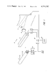
- FIG. 4 is an enlarged perspective view of one embodiment of light valve device in accordance with the present invention, which is useful, for example, in the FIG. 1 embodiment of the present invention;
- FIG. 5 is a diagram illustrating one preferred embodiment of addressing electronics for use with the light valve array shown in FIG. 4;
- FIG. 6 is a schematic perspective view showing one embodiment of a locationally-interlaced-scan device in accordance with the present invention.
- FIG. 7 is a schematic perspective view showing one embodiment of an area light valve device constructed in accordance with the present invention.
- the apparatus 10 comprises an illumination source 11 which directs flood illumination toward an imaging zone 12 via a light valve imaging device 13 and imaging lens 14.
- an illumination source 11 which directs flood illumination toward an imaging zone 12 via a light valve imaging device 13 and imaging lens 14.
- imaging device 13 it is the general function of such apparatus for imaging device 13 to modulate light from source 11, pixel by pixel, in accordance with the image to be reproduced.
- the light valve imaging device 13 is a linear array and is disposed to control the passage of light to successive transverse strip portions of a light-sensitive recording medium M as it is moved past the imaging zone 12, e.g. by drive means 15.
- Apparatus 10 is adapted for electronic color imaging, and separate red (R), green (G) and blue (B) light sources are provided at source 11 for sequential energization by control 15 during line imaging periods. It will be appreciated from the subsequent description that the structural approach of the present invention has significant advantage in many other electronic imaging configurations, e.g. where only one color light is used or in an area light valve array configuration where the image medium remains stationary during exposure.
- the linear light valve array 20 shown in FIG. 2 comprises a plurality of discrete, separately-addressable pixel portions P 1 , P 2 . . . P x on a PLZT panel 21 and cooperating crossed polarizers 22 and 23.
- Prior art address means for light valve array 20 is shown in more detail in FIG. 3 where it can be seen that pixel portions P 1 and P 2 are defined by a common ground electrode 24 and independently addressable electrodes 25, all formed on panel 21.
- High voltage electronic switches 26 e.g. transistor amplifiers
- each of the elements of shift register 27 are loaded with information signals ("V” or "O") in accordance with the appropriate "on or off” condition for the image pixel portion corresponding to its coupled pixel portion of the light valve array 20.
- the switches 26 Upon output of these signals from the shift register 27, the switches 26 appropriately energize, or leave unenergized, electrodes 25.
- each pixel portion of light valve array 20 requires its own high voltage electronic switch 26 to isolate the low-voltage signal circuitry, including shift register 27, from the high-voltage energizing circuitry including electrodes 25.
- light valve imaging device 13 comprises a high-resolution, locationally-addressing light valve array which includes addressable electro-optic panel 31, formed for example of PLZT ceramic material, and cooperating crossed polarizing means 32 and 33. It will be appreciated that although the portions of the FIG. 4 structure are shown in spaced relation, they usually will be contiguous.
- the panel 31 comprises a plurality of discrete pixel portions A 1 , A 2 . . . ; B 1 , B 2 . . .; C 1 , C 2 . .
- the addressing electrode structure can be like that shown in FIG. 3, or more preferably, like that disclosed in U.S. patent application Ser. No. 230,099, entitled “Light Valve Imaging Apparatus Having Improved Addressing Electrode Structure " and filed Jan. 29, 1981, in the names of J. M. Mir and J. R. Varner.
- the addressing electrodes within the different location-address sectors are energizable independently of the other electrodes comprising such a sector. That is, the addressing electrode for pixel portion A 1 is energizable independently of the electrodes for pixel portions A 2 , A 3 and A 4 .
- each addressing electrode, within the location-address sectors is electrically coupled to one corresponding addressing electrode in each of the other sectors.
- addressing electrodes of pixel portions A 1 , B 1 , C 1 , D 1 are connected to a common electrical bus line L 1 and form an inter-sector pixel portion group of the locationally-addressing light valve array.
- the A 2 , B 2 , C 2 electrodes are coupled to bus line L 2
- the A 3 , B 3 , C 3 electrodes are coupled to bus line L 3
- the A 4 , B 4 , C 4 electrodes are coupled to bus line L 4 to form other inter-sector groups.
- the electrode bus lines L 1 , L 2 , L 3 and L 4 respectively are coupled to high voltage switches 41, 42, 43 and 44, e.g. transistor amplifiers. Those switches are adapted to selectively energize their respective buses (and the coupled addressing electrodes) with a high voltage "V" in response to location-address signals from location-address means SR-2, e.g. a shift register or a resettable counter. For example, address means SR-2, bearing signals as indicated would activate switch 41 to an "on” condition but leave switches 42, 43, 44 in the "off" condition.
- SR-2 e.g. a shift register or a resettable counter.
- pixel portions A 1 , B 1 , C 1 , etc. would be turned to an "on” (light transmitting) condition by their addressing electrodes, but the remaining illustrated electrodes would remain “off”.
- switches 42, 43 and 44 are respectively switched “on” with all other switches “off” so that within each line period all pixel portions of the modulator panel 31 have been turned “on” in an interlaced fashion.
- the structure thus far described does not provide imagewise control of light passing to the exposure zone. Instead, it provides locationally-interlaced optical addressing of a line at imaging zone 12. Further, it should be noted at this stage, that only four high voltage switches are utilized for twelve pixels as compared to one for each pixel portion in prior art devices. It will be understood that the electronic economy of this configuration is significantly more than represented by the FIGS. 4 and 5 illustration, because light valve panels 31 for a complete line will have many more pixel portions than shown, e.g. 200 per inch.
- light valve imaging device 13 further comprises a low-resolution, informationally-addressing light valve array comprising addressable electro-optic panel 35 sandwiched between polarizers 34 and 36.
- Polarizer 34 has the same polarization direction as polarizer 33 and both are crossed with respect to polarizer 36. It can be seen that light introduced through polarizer 36 will only pass polarizers 33-34 if rotated 90° by the energization pixel portions A, B, C, etc., of panel 35.
- Polarizers 34-35 can be a single polarizing means; however, dual polarizers are preferred for maximum light contrast between on-off conditions.
- each of information-address sectors A, B, C of panel 35 have their addressing electrodes (not shown but preferably of the kind disclosed in aforementioned U.S. patent application Ser. No. 230,099) connectable to a source of high voltage "V" by high voltage switch means 45, 46, 47, respectively.
- Switch means 45, 46, 47 are in turn actuatable between an off-on condition by serial-in, parallel-out shift register SR-1.
- serial-in, parallel-out shift register SR-1 As described in more detail below, successive sets of information signals (each containing information representative of a plurality of spaced image pixels along a line of the image to be reproduced) are cyclically input to the shift register SR-1 and output in synchronization with the activation of switches 41-44 by SR-2, the energization of light source 11 and the movement of image medium M.
- color control 15 acting in response to signals from central processing unit (CPU) 49 and clock 50 effects at least three sequential light exposure periods, one each of red, green and blue light.
- locationally-addressing light valve panel 31 is actuated under control of unit 49 and SR-2, sequentially turning on the inter-sector pixel groups A, 1 , B 1 , C 1 , through A 4 , B 4 , C 4 , etc.
- appropriate image information is input to register SR-1 for informationally-addressing panel 35.
- information address sector A will be energized to an "on" condition during the sub-period of locational-address by panel 31 that energizes the inter-sector pixel group containing pixel portion A 1 . If the B 1 pixel of that line also required red light, information address sector B would also be energized during this sub-period; otherwise it would not.
- this sequence is repeated for each inter-sector group of locationally-addressing panel 31 and for each light color.
- FIG. 6 One preferred mode to obtain a properly formatted signal, directly from the detecting-scan of a record member to be reproduced, is illustrated in FIG. 6.
- This embodiment also illustrates the independent utility of the present invention's locationally-addressing, light valve array configuration as a detecting scanner.
- a record member T e.g. a transparency image to be reproduced by electronic imaging apparatus
- drive means 61 which is controlled, e.g. by a known servo device under the regulation of clock 50.
- clock 50 also regulates CPU 49 of imaging apparatus 10.
- Imaging optics 64 e.g. an array of gradient index fiber lenses, are located on the opposite side of the scan station and direct light that is transmitted by the transparency to light valve scan array 66.
- Array 66 is constructed with the same elements 31, 32, 33 as shown in FIG. 4 and has addressing means like that shown for panel 31 in FIG. 5.
- signals from detectors 71, 72, 73, etc. will comprise the proper image information (for each pixel portion of each line of the transparency T), in the proper format, to address to shift register SR-1 of apparatus 10 in proper timed relation with the activation of array 31 by its address means SR-2.
- the parallel signals from the detectors are transformed to a serial form by parallel-to-serial shift register 76, after having any desired image-enhancement signal processing performed thereon by image process and control logic 77.
- FIG. 6 scanner embodiment is one useful configuration
- record members to be reproduced can also be scanned by conventional scanners (e.g. flying spot scanners or CCD arrays).
- conventional scanners e.g. flying spot scanners or CCD arrays
- Proper signal formatting is then effected with dedicated hardware and/or software.
- area array 80 comprises high-resolution locationally-addressing panel 81 and low-resolution informationally-addressing panel 85.
- Area polarizers (not shown) are provided between and on each end of the light valve arrays, with polarization directions as described with respect to the FIG. 4 linear array configuration.
- a plurality of location-address means I, II, III, etc., each such as SR-2 shown in FIG. 5 for array 31, are provided respectively for each linear row of area array 81.
- information-address shift registers S-1, S-2, S-3 and S-4 are provided to control low-resolution information sectors I-A through IV-C, etc.
Abstract
Description
Claims (9)
Priority Applications (5)
| Application Number | Priority Date | Filing Date | Title |
|---|---|---|---|
| US06/268,975 US4374397A (en) | 1981-06-01 | 1981-06-01 | Light valve devices and electronic imaging/scan apparatus with locationally-interlaced optical addressing |
| PCT/US1982/000703 WO1982004367A1 (en) | 1981-06-01 | 1982-05-24 | Electronic imaging apparatus with light valve arrays |
| JP57502072A JPS58500881A (en) | 1981-06-01 | 1982-05-24 | Electronic imaging equipment including light valve array |
| EP19820902124 EP0079946A4 (en) | 1981-06-01 | 1982-05-24 | Electronic imaging apparatus with light valve arrays. |
| CA000404116A CA1171359A (en) | 1981-06-01 | 1982-05-31 | Light valve devices and electronic imaging/scan apparatus with locationally-interlaced, optical addressing |
Applications Claiming Priority (1)
| Application Number | Priority Date | Filing Date | Title |
|---|---|---|---|
| US06/268,975 US4374397A (en) | 1981-06-01 | 1981-06-01 | Light valve devices and electronic imaging/scan apparatus with locationally-interlaced optical addressing |
Publications (1)
| Publication Number | Publication Date |
|---|---|
| US4374397A true US4374397A (en) | 1983-02-15 |
Family
ID=23025322
Family Applications (1)
| Application Number | Title | Priority Date | Filing Date |
|---|---|---|---|
| US06/268,975 Expired - Lifetime US4374397A (en) | 1981-06-01 | 1981-06-01 | Light valve devices and electronic imaging/scan apparatus with locationally-interlaced optical addressing |
Country Status (5)
| Country | Link |
|---|---|
| US (1) | US4374397A (en) |
| EP (1) | EP0079946A4 (en) |
| JP (1) | JPS58500881A (en) |
| CA (1) | CA1171359A (en) |
| WO (1) | WO1982004367A1 (en) |
Cited By (66)
| Publication number | Priority date | Publication date | Assignee | Title |
|---|---|---|---|---|
| US4446479A (en) * | 1982-06-25 | 1984-05-01 | Eastman Kodak Company | Luminescent device for high resolution optical address and light valve imaging apparatus employing such device |
| US4469433A (en) * | 1981-10-30 | 1984-09-04 | Fuji Xerox Co., Ltd. | Color copying machine using signal conversion |
| US4797694A (en) * | 1987-09-23 | 1989-01-10 | Eastman Kodak Company | Scan-multiplexed light valve printer with band-reducing construction |
| EP0299257A1 (en) * | 1987-07-03 | 1989-01-18 | Nippon Telegraph And Telephone Corporation | Recording apparatus and recording method using the same |
| US4801194A (en) * | 1987-09-23 | 1989-01-31 | Eastman Kodak Company | Multiplexed array exposing system having equi-angular scan exposure regions |
| US4805012A (en) * | 1987-09-23 | 1989-02-14 | Eastman Kodak Company | System for high resolution exposure address with coarser resolution exposing array |
| US4916470A (en) * | 1988-11-16 | 1990-04-10 | Xerox Corporation | Image bar with electrochromic switching system |
| US5019898A (en) * | 1989-04-26 | 1991-05-28 | The California Institute Of Technology | Real-time pseudocolor density encoding of an image |
| US5646713A (en) * | 1995-06-13 | 1997-07-08 | Eastman Kodak Company | Apparatus and method for exposing data characters onto a strip region of moving photosensitive media |
| US5764280A (en) * | 1997-03-20 | 1998-06-09 | Silicon Light Machines Inc. | Display system including an image generator and movable scanner for same |
| US5982553A (en) * | 1997-03-20 | 1999-11-09 | Silicon Light Machines | Display device incorporating one-dimensional grating light-valve array |
| US6101036A (en) * | 1998-06-23 | 2000-08-08 | Silicon Light Machines | Embossed diffraction grating alone and in combination with changeable image display |
| US6130770A (en) * | 1998-06-23 | 2000-10-10 | Silicon Light Machines | Electron gun activated grating light valve |
| US6226029B1 (en) * | 1999-04-26 | 2001-05-01 | Xerox Corporation | Aerial slow scan position control using an electronically addressable liquid crystal plate |
| US20010022382A1 (en) * | 1998-07-29 | 2001-09-20 | Shook James Gill | Method of and apparatus for sealing an hermetic lid to a semiconductor die |
| US20020098610A1 (en) * | 2001-01-19 | 2002-07-25 | Alexander Payne | Reduced surface charging in silicon-based devices |
| US6437316B1 (en) * | 1996-11-04 | 2002-08-20 | Oridion Medical Ltd. | Fluid analyzer with tube connector verifier |
| US20020186448A1 (en) * | 2001-04-10 | 2002-12-12 | Silicon Light Machines | Angled illumination for a single order GLV based projection system |
| US20020196492A1 (en) * | 2001-06-25 | 2002-12-26 | Silicon Light Machines | Method and apparatus for dynamic equalization in wavelength division multiplexing |
| US20030025984A1 (en) * | 2001-08-01 | 2003-02-06 | Chris Gudeman | Optical mem device with encapsulated dampening gas |
| US20030035189A1 (en) * | 2001-08-15 | 2003-02-20 | Amm David T. | Stress tuned blazed grating light valve |
| US20030038943A1 (en) * | 2001-08-21 | 2003-02-27 | Kais Almarzouk | Method and apparatus for measuring wavelength jitter of light signal |
| US20030103194A1 (en) * | 2001-11-30 | 2003-06-05 | Gross Kenneth P. | Display apparatus including RGB color combiner and 1D light valve relay including schlieren filter |
| US20040001257A1 (en) * | 2001-03-08 | 2004-01-01 | Akira Tomita | High contrast grating light valve |
| US20040001264A1 (en) * | 2002-06-28 | 2004-01-01 | Christopher Gudeman | Micro-support structures |
| US20040008399A1 (en) * | 2001-06-25 | 2004-01-15 | Trisnadi Jahja I. | Method, apparatus, and diffuser for reducing laser speckle |
| US20040057101A1 (en) * | 2002-06-28 | 2004-03-25 | James Hunter | Reduced formation of asperities in contact micro-structures |
| US6712480B1 (en) | 2002-09-27 | 2004-03-30 | Silicon Light Machines | Controlled curvature of stressed micro-structures |
| US6714337B1 (en) | 2002-06-28 | 2004-03-30 | Silicon Light Machines | Method and device for modulating a light beam and having an improved gamma response |
| US6728023B1 (en) | 2002-05-28 | 2004-04-27 | Silicon Light Machines | Optical device arrays with optimized image resolution |
| US6767751B2 (en) | 2002-05-28 | 2004-07-27 | Silicon Light Machines, Inc. | Integrated driver process flow |
| US6800238B1 (en) | 2002-01-15 | 2004-10-05 | Silicon Light Machines, Inc. | Method for domain patterning in low coercive field ferroelectrics |
| US6801354B1 (en) | 2002-08-20 | 2004-10-05 | Silicon Light Machines, Inc. | 2-D diffraction grating for substantially eliminating polarization dependent losses |
| US6806997B1 (en) | 2003-02-28 | 2004-10-19 | Silicon Light Machines, Inc. | Patterned diffractive light modulator ribbon for PDL reduction |
| US6822797B1 (en) | 2002-05-31 | 2004-11-23 | Silicon Light Machines, Inc. | Light modulator structure for producing high-contrast operation using zero-order light |
| US6829258B1 (en) | 2002-06-26 | 2004-12-07 | Silicon Light Machines, Inc. | Rapidly tunable external cavity laser |
| US6829092B2 (en) | 2001-08-15 | 2004-12-07 | Silicon Light Machines, Inc. | Blazed grating light valve |
| US20050024706A1 (en) * | 2003-07-29 | 2005-02-03 | Daniel Gelbart | Non-uniform light valve |
| US6865346B1 (en) | 2001-06-05 | 2005-03-08 | Silicon Light Machines Corporation | Fiber optic transceiver |
| US6872984B1 (en) | 1998-07-29 | 2005-03-29 | Silicon Light Machines Corporation | Method of sealing a hermetic lid to a semiconductor die at an angle |
| US6922273B1 (en) | 2003-02-28 | 2005-07-26 | Silicon Light Machines Corporation | PDL mitigation structure for diffractive MEMS and gratings |
| US6922272B1 (en) | 2003-02-14 | 2005-07-26 | Silicon Light Machines Corporation | Method and apparatus for leveling thermal stress variations in multi-layer MEMS devices |
| US6927891B1 (en) | 2002-12-23 | 2005-08-09 | Silicon Light Machines Corporation | Tilt-able grating plane for improved crosstalk in 1×N blaze switches |
| US6928207B1 (en) | 2002-12-12 | 2005-08-09 | Silicon Light Machines Corporation | Apparatus for selectively blocking WDM channels |
| US6934070B1 (en) | 2002-12-18 | 2005-08-23 | Silicon Light Machines Corporation | Chirped optical MEM device |
| US6947613B1 (en) | 2003-02-11 | 2005-09-20 | Silicon Light Machines Corporation | Wavelength selective switch and equalizer |
| US6956878B1 (en) | 2000-02-07 | 2005-10-18 | Silicon Light Machines Corporation | Method and apparatus for reducing laser speckle using polarization averaging |
| US6956995B1 (en) | 2001-11-09 | 2005-10-18 | Silicon Light Machines Corporation | Optical communication arrangement |
| US6987600B1 (en) | 2002-12-17 | 2006-01-17 | Silicon Light Machines Corporation | Arbitrary phase profile for better equalization in dynamic gain equalizer |
| US6991953B1 (en) | 2001-09-13 | 2006-01-31 | Silicon Light Machines Corporation | Microelectronic mechanical system and methods |
| US7027202B1 (en) | 2003-02-28 | 2006-04-11 | Silicon Light Machines Corp | Silicon substrate as a light modulator sacrificial layer |
| US20060082874A1 (en) * | 2004-10-19 | 2006-04-20 | Anderson Daryl E | Display device |
| US7042611B1 (en) | 2003-03-03 | 2006-05-09 | Silicon Light Machines Corporation | Pre-deflected bias ribbons |
| US7054515B1 (en) | 2002-05-30 | 2006-05-30 | Silicon Light Machines Corporation | Diffractive light modulator-based dynamic equalizer with integrated spectral monitor |
| US7057795B2 (en) | 2002-08-20 | 2006-06-06 | Silicon Light Machines Corporation | Micro-structures with individually addressable ribbon pairs |
| US7057819B1 (en) | 2002-12-17 | 2006-06-06 | Silicon Light Machines Corporation | High contrast tilting ribbon blazed grating |
| US7068372B1 (en) | 2003-01-28 | 2006-06-27 | Silicon Light Machines Corporation | MEMS interferometer-based reconfigurable optical add-and-drop multiplexor |
| US20070146257A1 (en) * | 2002-03-13 | 2007-06-28 | The University Of British Columbia | Motion-blur compensation in backlit displays |
| US7286764B1 (en) | 2003-02-03 | 2007-10-23 | Silicon Light Machines Corporation | Reconfigurable modulator-based optical add-and-drop multiplexer |
| US7391973B1 (en) | 2003-02-28 | 2008-06-24 | Silicon Light Machines Corporation | Two-stage gain equalizer |
| US20090085929A1 (en) * | 2001-02-27 | 2009-04-02 | Dolby Laboratories Licensing Corporation | Hdr displays and control systems therefor |
| US20100002026A1 (en) * | 2007-02-01 | 2010-01-07 | Dolby Laboratories Licensing Corporation | Calibration of displays having spatially-variable backlight |
| US20100214282A1 (en) * | 2009-02-24 | 2010-08-26 | Dolby Laboratories Licensing Corporation | Apparatus for providing light source modulation in dual modulator displays |
| US8482698B2 (en) | 2008-06-25 | 2013-07-09 | Dolby Laboratories Licensing Corporation | High dynamic range display using LED backlighting, stacked optical films, and LCD drive signals based on a low resolution light field simulation |
| US8687271B2 (en) | 2002-03-13 | 2014-04-01 | Dolby Laboratories Licensing Corporation | N-modulation displays and related methods |
| US8720772B2 (en) | 2007-12-31 | 2014-05-13 | Oridion Medical 1987 Ltd. | Tube verifier |
Citations (8)
| Publication number | Priority date | Publication date | Assignee | Title |
|---|---|---|---|---|
| US3428743A (en) * | 1966-02-07 | 1969-02-18 | Thomas F Hanlon | Electrooptic crystal controlled variable color modulator |
| US3470310A (en) * | 1966-05-23 | 1969-09-30 | Rca Corp | Color image display system utilizing a light valve |
| US3891560A (en) * | 1974-01-28 | 1975-06-24 | Hughes Aircraft Co | Large screen color display |
| US3930119A (en) * | 1973-05-04 | 1975-12-30 | Philips Corp | Facsimile apparatus for writing and reading mechanically moving documents |
| US4129357A (en) * | 1977-08-11 | 1978-12-12 | Nasa | Partial polarizer filter |
| US4229095A (en) * | 1979-01-29 | 1980-10-21 | Eastman Kodak Company | Electro-optical color imaging apparatus |
| US4294524A (en) * | 1978-06-29 | 1981-10-13 | Michael Stolov | Image or picture projecting system using electronically controlled slides |
| US4316196A (en) * | 1977-03-10 | 1982-02-16 | Bell & Howell Corporation | Illumination and light gate utilization methods and apparatus |
Family Cites Families (3)
| Publication number | Priority date | Publication date | Assignee | Title |
|---|---|---|---|---|
| US3982239A (en) * | 1973-02-07 | 1976-09-21 | North Hills Electronics, Inc. | Saturation drive arrangements for optically bistable displays |
| FR2410924A1 (en) * | 1977-12-01 | 1979-06-29 | Thomson Csf | FAXING PROCESS USING A SMECTIC LIQUID CRYSTAL CELL AND TRANSMITTER-RECEIVER FACSIMILE IMPLEMENTING THIS PROCESS |
| DE3018452C2 (en) * | 1980-05-14 | 1983-11-10 | Standard Elektrik Lorenz Ag, 7000 Stuttgart | Facsimile writing device |
-
1981
- 1981-06-01 US US06/268,975 patent/US4374397A/en not_active Expired - Lifetime
-
1982
- 1982-05-24 EP EP19820902124 patent/EP0079946A4/en not_active Withdrawn
- 1982-05-24 WO PCT/US1982/000703 patent/WO1982004367A1/en not_active Application Discontinuation
- 1982-05-24 JP JP57502072A patent/JPS58500881A/en active Granted
- 1982-05-31 CA CA000404116A patent/CA1171359A/en not_active Expired
Patent Citations (8)
| Publication number | Priority date | Publication date | Assignee | Title |
|---|---|---|---|---|
| US3428743A (en) * | 1966-02-07 | 1969-02-18 | Thomas F Hanlon | Electrooptic crystal controlled variable color modulator |
| US3470310A (en) * | 1966-05-23 | 1969-09-30 | Rca Corp | Color image display system utilizing a light valve |
| US3930119A (en) * | 1973-05-04 | 1975-12-30 | Philips Corp | Facsimile apparatus for writing and reading mechanically moving documents |
| US3891560A (en) * | 1974-01-28 | 1975-06-24 | Hughes Aircraft Co | Large screen color display |
| US4316196A (en) * | 1977-03-10 | 1982-02-16 | Bell & Howell Corporation | Illumination and light gate utilization methods and apparatus |
| US4129357A (en) * | 1977-08-11 | 1978-12-12 | Nasa | Partial polarizer filter |
| US4294524A (en) * | 1978-06-29 | 1981-10-13 | Michael Stolov | Image or picture projecting system using electronically controlled slides |
| US4229095A (en) * | 1979-01-29 | 1980-10-21 | Eastman Kodak Company | Electro-optical color imaging apparatus |
Cited By (119)
| Publication number | Priority date | Publication date | Assignee | Title |
|---|---|---|---|---|
| US4469433A (en) * | 1981-10-30 | 1984-09-04 | Fuji Xerox Co., Ltd. | Color copying machine using signal conversion |
| US4446479A (en) * | 1982-06-25 | 1984-05-01 | Eastman Kodak Company | Luminescent device for high resolution optical address and light valve imaging apparatus employing such device |
| US4899224A (en) * | 1987-07-03 | 1990-02-06 | Nippon Telegraph And Telephone Corporation | Recording apparatus and method utilizing an array of liquid crystal cells |
| EP0299257A1 (en) * | 1987-07-03 | 1989-01-18 | Nippon Telegraph And Telephone Corporation | Recording apparatus and recording method using the same |
| US4801194A (en) * | 1987-09-23 | 1989-01-31 | Eastman Kodak Company | Multiplexed array exposing system having equi-angular scan exposure regions |
| US4805012A (en) * | 1987-09-23 | 1989-02-14 | Eastman Kodak Company | System for high resolution exposure address with coarser resolution exposing array |
| US4797694A (en) * | 1987-09-23 | 1989-01-10 | Eastman Kodak Company | Scan-multiplexed light valve printer with band-reducing construction |
| US4916470A (en) * | 1988-11-16 | 1990-04-10 | Xerox Corporation | Image bar with electrochromic switching system |
| US5019898A (en) * | 1989-04-26 | 1991-05-28 | The California Institute Of Technology | Real-time pseudocolor density encoding of an image |
| US5646713A (en) * | 1995-06-13 | 1997-07-08 | Eastman Kodak Company | Apparatus and method for exposing data characters onto a strip region of moving photosensitive media |
| US6437316B1 (en) * | 1996-11-04 | 2002-08-20 | Oridion Medical Ltd. | Fluid analyzer with tube connector verifier |
| US5764280A (en) * | 1997-03-20 | 1998-06-09 | Silicon Light Machines Inc. | Display system including an image generator and movable scanner for same |
| US5982553A (en) * | 1997-03-20 | 1999-11-09 | Silicon Light Machines | Display device incorporating one-dimensional grating light-valve array |
| US6101036A (en) * | 1998-06-23 | 2000-08-08 | Silicon Light Machines | Embossed diffraction grating alone and in combination with changeable image display |
| US6130770A (en) * | 1998-06-23 | 2000-10-10 | Silicon Light Machines | Electron gun activated grating light valve |
| US6764875B2 (en) | 1998-07-29 | 2004-07-20 | Silicon Light Machines | Method of and apparatus for sealing an hermetic lid to a semiconductor die |
| US20010022382A1 (en) * | 1998-07-29 | 2001-09-20 | Shook James Gill | Method of and apparatus for sealing an hermetic lid to a semiconductor die |
| US6872984B1 (en) | 1998-07-29 | 2005-03-29 | Silicon Light Machines Corporation | Method of sealing a hermetic lid to a semiconductor die at an angle |
| US6226029B1 (en) * | 1999-04-26 | 2001-05-01 | Xerox Corporation | Aerial slow scan position control using an electronically addressable liquid crystal plate |
| US6956878B1 (en) | 2000-02-07 | 2005-10-18 | Silicon Light Machines Corporation | Method and apparatus for reducing laser speckle using polarization averaging |
| US20020098610A1 (en) * | 2001-01-19 | 2002-07-25 | Alexander Payne | Reduced surface charging in silicon-based devices |
| US7753530B2 (en) | 2001-02-27 | 2010-07-13 | Dolby Laboratories Licensing Corporation | HDR displays and control systems therefor |
| US9804487B2 (en) | 2001-02-27 | 2017-10-31 | Dolby Laboratories Licensing Corporation | Projection displays |
| US20090180078A1 (en) * | 2001-02-27 | 2009-07-16 | Lorne Whitehead | High dynamic range display devices having color light sources |
| US8684533B2 (en) | 2001-02-27 | 2014-04-01 | Dolby Laboratories Licensing Corporation | Projection displays |
| US7801426B2 (en) | 2001-02-27 | 2010-09-21 | Dolby Laboratories Licensing Corporation | High dynamic range display devices having color light sources |
| US8419194B2 (en) | 2001-02-27 | 2013-04-16 | Dolby Laboratories Licensing Corporation | Locally dimmed display |
| US8408718B2 (en) | 2001-02-27 | 2013-04-02 | Dolby Laboratories Licensing Corporation | Locally dimmed display |
| US20100302480A1 (en) * | 2001-02-27 | 2010-12-02 | Lorne Whitehead | Edge lit locally dimmed display |
| US10261405B2 (en) | 2001-02-27 | 2019-04-16 | Dolby Laboratories Licensing Corporation | Projection displays |
| US20090284547A1 (en) * | 2001-02-27 | 2009-11-19 | Dolby Laboratories Licensing Corporation | Hdr displays and control systems therefor |
| US7942531B2 (en) | 2001-02-27 | 2011-05-17 | Dolby Laboratories Licensing Corporation | Edge lit locally dimmed display |
| US20110216387A1 (en) * | 2001-02-27 | 2011-09-08 | Dolby Laboratories Licensing Corporation | Edge lit locally dimmed display |
| US8277056B2 (en) * | 2001-02-27 | 2012-10-02 | Dolby Laboratories Licensing Corporation | Locally dimmed display |
| US8172401B2 (en) | 2001-02-27 | 2012-05-08 | Dolby Laboratories Licensing Corporation | Edge lit locally dimmed display |
| US7731367B2 (en) | 2001-02-27 | 2010-06-08 | Dolby Laboratories Licensing Corporation | HDR displays and control systems therefor |
| US20120188296A1 (en) * | 2001-02-27 | 2012-07-26 | Dolby Laboratories Licensing Corporation | Locally dimmed display |
| US20090085929A1 (en) * | 2001-02-27 | 2009-04-02 | Dolby Laboratories Licensing Corporation | Hdr displays and control systems therefor |
| US9412337B2 (en) | 2001-02-27 | 2016-08-09 | Dolby Laboratories Licensing Corporation | Projection displays |
| US7177081B2 (en) | 2001-03-08 | 2007-02-13 | Silicon Light Machines Corporation | High contrast grating light valve type device |
| US20040001257A1 (en) * | 2001-03-08 | 2004-01-01 | Akira Tomita | High contrast grating light valve |
| US6707591B2 (en) | 2001-04-10 | 2004-03-16 | Silicon Light Machines | Angled illumination for a single order light modulator based projection system |
| US20020186448A1 (en) * | 2001-04-10 | 2002-12-12 | Silicon Light Machines | Angled illumination for a single order GLV based projection system |
| US6865346B1 (en) | 2001-06-05 | 2005-03-08 | Silicon Light Machines Corporation | Fiber optic transceiver |
| US20020196492A1 (en) * | 2001-06-25 | 2002-12-26 | Silicon Light Machines | Method and apparatus for dynamic equalization in wavelength division multiplexing |
| US20040008399A1 (en) * | 2001-06-25 | 2004-01-15 | Trisnadi Jahja I. | Method, apparatus, and diffuser for reducing laser speckle |
| US6782205B2 (en) | 2001-06-25 | 2004-08-24 | Silicon Light Machines | Method and apparatus for dynamic equalization in wavelength division multiplexing |
| US6747781B2 (en) | 2001-06-25 | 2004-06-08 | Silicon Light Machines, Inc. | Method, apparatus, and diffuser for reducing laser speckle |
| US20030025984A1 (en) * | 2001-08-01 | 2003-02-06 | Chris Gudeman | Optical mem device with encapsulated dampening gas |
| US6829092B2 (en) | 2001-08-15 | 2004-12-07 | Silicon Light Machines, Inc. | Blazed grating light valve |
| US20030035189A1 (en) * | 2001-08-15 | 2003-02-20 | Amm David T. | Stress tuned blazed grating light valve |
| US20030038943A1 (en) * | 2001-08-21 | 2003-02-27 | Kais Almarzouk | Method and apparatus for measuring wavelength jitter of light signal |
| US6991953B1 (en) | 2001-09-13 | 2006-01-31 | Silicon Light Machines Corporation | Microelectronic mechanical system and methods |
| US7049164B2 (en) | 2001-09-13 | 2006-05-23 | Silicon Light Machines Corporation | Microelectronic mechanical system and methods |
| US6956995B1 (en) | 2001-11-09 | 2005-10-18 | Silicon Light Machines Corporation | Optical communication arrangement |
| US20030103194A1 (en) * | 2001-11-30 | 2003-06-05 | Gross Kenneth P. | Display apparatus including RGB color combiner and 1D light valve relay including schlieren filter |
| US6800238B1 (en) | 2002-01-15 | 2004-10-05 | Silicon Light Machines, Inc. | Method for domain patterning in low coercive field ferroelectrics |
| US7800822B2 (en) | 2002-03-13 | 2010-09-21 | Dolby Laboratories Licensing Corporation | HDR displays with individually-controllable color backlights |
| US7777945B2 (en) | 2002-03-13 | 2010-08-17 | Dolby Laboratories Licensing Corporation | HDR displays having light estimating controllers |
| US9270956B2 (en) | 2002-03-13 | 2016-02-23 | Dolby Laboratories Licensing Corporation | Image display |
| US8199401B2 (en) | 2002-03-13 | 2012-06-12 | Dolby Laboratories Licensing Corporation | N-modulation displays and related methods |
| US8890799B2 (en) | 2002-03-13 | 2014-11-18 | Dolby Laboratories Licensing Corporation | Display with red, green, and blue light sources |
| US8687271B2 (en) | 2002-03-13 | 2014-04-01 | Dolby Laboratories Licensing Corporation | N-modulation displays and related methods |
| US8446351B2 (en) | 2002-03-13 | 2013-05-21 | Dolby Laboratories Licensing Corporation | Edge lit LED based locally dimmed display |
| US10416480B2 (en) | 2002-03-13 | 2019-09-17 | Dolby Laboratories Licensing Corporation | Image display |
| US8059110B2 (en) | 2002-03-13 | 2011-11-15 | Dolby Laboratories Licensing Corporation | Motion-blur compensation in backlit displays |
| US20100007577A1 (en) * | 2002-03-13 | 2010-01-14 | Ajit Ninan | N-modulation displays and related methods |
| US11378840B2 (en) | 2002-03-13 | 2022-07-05 | Dolby Laboratories Licensing Corporation | Image display |
| US20070146257A1 (en) * | 2002-03-13 | 2007-06-28 | The University Of British Columbia | Motion-blur compensation in backlit displays |
| US20070268211A1 (en) * | 2002-03-13 | 2007-11-22 | Dolby Canada Coporation | Hdr displays with individually-controllable color backlights |
| US8125425B2 (en) | 2002-03-13 | 2012-02-28 | Dolby Laboratories Licensing Corporation | HDR displays with dual modulators having different resolutions |
| US6728023B1 (en) | 2002-05-28 | 2004-04-27 | Silicon Light Machines | Optical device arrays with optimized image resolution |
| US6767751B2 (en) | 2002-05-28 | 2004-07-27 | Silicon Light Machines, Inc. | Integrated driver process flow |
| US7054515B1 (en) | 2002-05-30 | 2006-05-30 | Silicon Light Machines Corporation | Diffractive light modulator-based dynamic equalizer with integrated spectral monitor |
| US6822797B1 (en) | 2002-05-31 | 2004-11-23 | Silicon Light Machines, Inc. | Light modulator structure for producing high-contrast operation using zero-order light |
| US6829258B1 (en) | 2002-06-26 | 2004-12-07 | Silicon Light Machines, Inc. | Rapidly tunable external cavity laser |
| US6714337B1 (en) | 2002-06-28 | 2004-03-30 | Silicon Light Machines | Method and device for modulating a light beam and having an improved gamma response |
| US6813059B2 (en) | 2002-06-28 | 2004-11-02 | Silicon Light Machines, Inc. | Reduced formation of asperities in contact micro-structures |
| US20040001264A1 (en) * | 2002-06-28 | 2004-01-01 | Christopher Gudeman | Micro-support structures |
| US20040057101A1 (en) * | 2002-06-28 | 2004-03-25 | James Hunter | Reduced formation of asperities in contact micro-structures |
| US6908201B2 (en) | 2002-06-28 | 2005-06-21 | Silicon Light Machines Corporation | Micro-support structures |
| US6801354B1 (en) | 2002-08-20 | 2004-10-05 | Silicon Light Machines, Inc. | 2-D diffraction grating for substantially eliminating polarization dependent losses |
| US7057795B2 (en) | 2002-08-20 | 2006-06-06 | Silicon Light Machines Corporation | Micro-structures with individually addressable ribbon pairs |
| US6712480B1 (en) | 2002-09-27 | 2004-03-30 | Silicon Light Machines | Controlled curvature of stressed micro-structures |
| US6928207B1 (en) | 2002-12-12 | 2005-08-09 | Silicon Light Machines Corporation | Apparatus for selectively blocking WDM channels |
| US7057819B1 (en) | 2002-12-17 | 2006-06-06 | Silicon Light Machines Corporation | High contrast tilting ribbon blazed grating |
| US6987600B1 (en) | 2002-12-17 | 2006-01-17 | Silicon Light Machines Corporation | Arbitrary phase profile for better equalization in dynamic gain equalizer |
| US6934070B1 (en) | 2002-12-18 | 2005-08-23 | Silicon Light Machines Corporation | Chirped optical MEM device |
| US6927891B1 (en) | 2002-12-23 | 2005-08-09 | Silicon Light Machines Corporation | Tilt-able grating plane for improved crosstalk in 1×N blaze switches |
| US7068372B1 (en) | 2003-01-28 | 2006-06-27 | Silicon Light Machines Corporation | MEMS interferometer-based reconfigurable optical add-and-drop multiplexor |
| US7286764B1 (en) | 2003-02-03 | 2007-10-23 | Silicon Light Machines Corporation | Reconfigurable modulator-based optical add-and-drop multiplexer |
| US6947613B1 (en) | 2003-02-11 | 2005-09-20 | Silicon Light Machines Corporation | Wavelength selective switch and equalizer |
| US6922272B1 (en) | 2003-02-14 | 2005-07-26 | Silicon Light Machines Corporation | Method and apparatus for leveling thermal stress variations in multi-layer MEMS devices |
| US7027202B1 (en) | 2003-02-28 | 2006-04-11 | Silicon Light Machines Corp | Silicon substrate as a light modulator sacrificial layer |
| US6806997B1 (en) | 2003-02-28 | 2004-10-19 | Silicon Light Machines, Inc. | Patterned diffractive light modulator ribbon for PDL reduction |
| US6922273B1 (en) | 2003-02-28 | 2005-07-26 | Silicon Light Machines Corporation | PDL mitigation structure for diffractive MEMS and gratings |
| US7391973B1 (en) | 2003-02-28 | 2008-06-24 | Silicon Light Machines Corporation | Two-stage gain equalizer |
| US7042611B1 (en) | 2003-03-03 | 2006-05-09 | Silicon Light Machines Corporation | Pre-deflected bias ribbons |
| US20050024706A1 (en) * | 2003-07-29 | 2005-02-03 | Daniel Gelbart | Non-uniform light valve |
| CN100434960C (en) * | 2003-07-29 | 2008-11-19 | 加拿大柯达图形通信公司 | Non-uniform light valve |
| US7042624B2 (en) * | 2003-07-29 | 2006-05-09 | Kodak Graphic Communications, Canada Company | Non-uniform light valve |
| US7733298B2 (en) | 2004-10-19 | 2010-06-08 | Hewlett-Packard Development Company, L.P. | Display device |
| US20060082874A1 (en) * | 2004-10-19 | 2006-04-20 | Anderson Daryl E | Display device |
| US20100002026A1 (en) * | 2007-02-01 | 2010-01-07 | Dolby Laboratories Licensing Corporation | Calibration of displays having spatially-variable backlight |
| US8471807B2 (en) | 2007-02-01 | 2013-06-25 | Dolby Laboratories Licensing Corporation | Calibration of displays having spatially-variable backlight |
| US9480832B2 (en) | 2007-12-31 | 2016-11-01 | Oridion Medical 1987 Ltd. | Tube verifier |
| US8720772B2 (en) | 2007-12-31 | 2014-05-13 | Oridion Medical 1987 Ltd. | Tube verifier |
| US8763892B2 (en) | 2007-12-31 | 2014-07-01 | Oridon Medical 1987 Ltd. | Tube verifier |
| US9206932B2 (en) | 2007-12-31 | 2015-12-08 | Oridion Medical (1987) Ltd. | Tube verifier |
| US8967461B2 (en) | 2007-12-31 | 2015-03-03 | Oridion Medical (1987) Ltd. | Tube verifier |
| US8763895B2 (en) | 2007-12-31 | 2014-07-01 | Oridion Medical 1987 Ltd. | Tube verifier |
| US8482698B2 (en) | 2008-06-25 | 2013-07-09 | Dolby Laboratories Licensing Corporation | High dynamic range display using LED backlighting, stacked optical films, and LCD drive signals based on a low resolution light field simulation |
| US9711111B2 (en) | 2008-06-25 | 2017-07-18 | Dolby Laboratories Licensing Corporation | High dynamic range display using LED backlighting, stacked optical films, and LCD drive signals based on a low resolution light field simulation |
| US10607569B2 (en) | 2008-06-25 | 2020-03-31 | Dolby Laboratories Licensing Corporation | High dynamic range display using LED backlighting, stacked optical films, and LCD drive signals based on a low resolution light field simulation |
| US9478182B2 (en) | 2009-02-24 | 2016-10-25 | Dolby Laboratories Licensing Corporation | Locally dimmed quantum dots (nano-crystal) based display |
| US10373574B2 (en) | 2009-02-24 | 2019-08-06 | Dolby Laboratories Licensing Corporation | Locally dimmed quantum dot display |
| US20100214282A1 (en) * | 2009-02-24 | 2010-08-26 | Dolby Laboratories Licensing Corporation | Apparatus for providing light source modulation in dual modulator displays |
| US9911389B2 (en) | 2009-02-24 | 2018-03-06 | Dolby Laboratories Licensing Corporation | Locally dimmed quantum dot display |
| US9099046B2 (en) | 2009-02-24 | 2015-08-04 | Dolby Laboratories Licensing Corporation | Apparatus for providing light source modulation in dual modulator displays |
Also Published As
| Publication number | Publication date |
|---|---|
| EP0079946A4 (en) | 1986-01-20 |
| WO1982004367A1 (en) | 1982-12-09 |
| CA1171359A (en) | 1984-07-24 |
| EP0079946A1 (en) | 1983-06-01 |
| JPS58500881A (en) | 1983-05-26 |
| JPH0430222B2 (en) | 1992-05-21 |
Similar Documents
| Publication | Publication Date | Title |
|---|---|---|
| US4374397A (en) | Light valve devices and electronic imaging/scan apparatus with locationally-interlaced optical addressing | |
| US4229095A (en) | Electro-optical color imaging apparatus | |
| US4377753A (en) | High resolution optical-addressing device and electronic scanner and/or printer apparatus employing such device | |
| EP0070298B1 (en) | Areal electronic imaging apparatus | |
| US4378568A (en) | Light valve imaging apparatus and method for providing gray scale | |
| US4378567A (en) | Electronic imaging apparatus having means for reducing inter-pixel transmission nonuniformity | |
| US4367946A (en) | Light valve imaging apparatus having improved optical configuration | |
| US4375647A (en) | Light valve scanner and scanner/printer apparatus for color originals | |
| US4449153A (en) | Light valve imaging apparatus and method having supplemental exposure control | |
| US4366500A (en) | Electronic color imaging apparatus having integral multicolor arrays | |
| US4366499A (en) | Electronic color imaging apparatus having improved color control device | |
| US4375649A (en) | Scanning device with area-to-linear mapping and related electronic scanner/printer apparatus | |
| US4458989A (en) | Electro-optic addressing apparatus and novel modulator configurations for use therein | |
| US4375648A (en) | High-resolution light valve apparatus for electronic imaging | |
| US4805012A (en) | System for high resolution exposure address with coarser resolution exposing array | |
| US4357625A (en) | Light valve imaging apparatus having enlarged pixel exposing regions | |
| US4822148A (en) | Multicolor light valve imaging apparatus having electrode constructions for uniform transmission | |
| US4446479A (en) | Luminescent device for high resolution optical address and light valve imaging apparatus employing such device | |
| JPH02245776A (en) | Method and apparatus for image exposure to phtosensitive medium using numeros optical valves | |
| EP0000603B1 (en) | Photoelectrophoretic multicolour imaging apparatus | |
| JPH0244303Y2 (en) | ||
| JPS6333969A (en) | Color picture reader |
Legal Events
| Date | Code | Title | Description |
|---|---|---|---|
| AS | Assignment |
Owner name: EASTMAN KODAK COMPANY, ROCHESTER, NY. A CORP.OF NJ Free format text: ASSIGNMENT OF ASSIGNORS INTEREST.;ASSIGNOR:MIR, JOSE' M.;REEL/FRAME:003947/0034 Effective date: 19810527 Owner name: EASTMAN KODAK COMPANY, ROCHESTER, NY. A CORP.OF, N Free format text: ASSIGNMENT OF ASSIGNORS INTEREST;ASSIGNOR:MIR, JOSE' M.;REEL/FRAME:003947/0034 Effective date: 19810527 |
|
| STCF | Information on status: patent grant |
Free format text: PATENTED CASE |
|
| MAFP | Maintenance fee payment |
Free format text: PAYMENT OF MAINTENANCE FEE, 4TH YEAR, PL 96-517 (ORIGINAL EVENT CODE: M170); ENTITY STATUS OF PATENT OWNER: LARGE ENTITY Year of fee payment: 4 |
|
| FEPP | Fee payment procedure |
Free format text: PAYOR NUMBER ASSIGNED (ORIGINAL EVENT CODE: ASPN); ENTITY STATUS OF PATENT OWNER: LARGE ENTITY |
|
| MAFP | Maintenance fee payment |
Free format text: PAYMENT OF MAINTENANCE FEE, 8TH YEAR, PL 96-517 (ORIGINAL EVENT CODE: M171); ENTITY STATUS OF PATENT OWNER: LARGE ENTITY Year of fee payment: 8 |
|
| MAFP | Maintenance fee payment |
Free format text: PAYMENT OF MAINTENANCE FEE, 12TH YEAR, LARGE ENTITY (ORIGINAL EVENT CODE: M185); ENTITY STATUS OF PATENT OWNER: LARGE ENTITY Year of fee payment: 12 |