US4400734A - Column defect compensating apparatus for CCD image sensor - Google Patents

Column defect compensating apparatus for CCD image sensor Download PDF

Info

Publication number
US4400734A
US4400734A US06/315,762 US31576281A US4400734A US 4400734 A US4400734 A US 4400734A US 31576281 A US31576281 A US 31576281A US 4400734 A US4400734 A US 4400734A
Authority
US
United States
Prior art keywords
shift register
charge
output
columns
auxiliary
Prior art date
Legal status (The legal status is an assumption and is not a legal conclusion. Google has not performed a legal analysis and makes no representation as to the accuracy of the status listed.)
Expired - Fee Related
Application number
US06/315,762
Inventor
Lee N. Davy
Current Assignee (The listed assignees may be inaccurate. Google has not performed a legal analysis and makes no representation or warranty as to the accuracy of the list.)
Eastman Kodak Co
Original Assignee
Eastman Kodak Co
Priority date (The priority date is an assumption and is not a legal conclusion. Google has not performed a legal analysis and makes no representation as to the accuracy of the date listed.)
Filing date
Publication date
Application filed by Eastman Kodak Co filed Critical Eastman Kodak Co
Priority to US06/315,762 priority Critical patent/US4400734A/en
Assigned to EASTMAN KODAK COMPANY reassignment EASTMAN KODAK COMPANY ASSIGNMENT OF ASSIGNORS INTEREST. Assignors: DAVY, LEE N.
Application granted granted Critical
Publication of US4400734A publication Critical patent/US4400734A/en
Anticipated expiration legal-status Critical
Expired - Fee Related legal-status Critical Current

Links

Images

Classifications

    • HELECTRICITY
    • H04ELECTRIC COMMUNICATION TECHNIQUE
    • H04NPICTORIAL COMMUNICATION, e.g. TELEVISION
    • H04N25/00Circuitry of solid-state image sensors [SSIS]; Control thereof
    • H04N25/60Noise processing, e.g. detecting, correcting, reducing or removing noise
    • H04N25/63Noise processing, e.g. detecting, correcting, reducing or removing noise applied to dark current

Definitions

  • the present invention relates to solid state charge coupled device image sensors and more particularly to apparatus for compensating for column defects in such image sensors.
  • CCD solid state charge coupled device
  • the disclosed scheme would contain one correction code word for each element in a defective column, e.g. 500 correction words if the sensor had 500 rows of sensor elements.
  • a column defect compensating apparatus having an auxiliary shift register with a plurality of cells corresponding to the columns of the two dimensional array.
  • the auxiliary shift register contains signals representing the condition of the columns, and is clocked in synchronism with the output shift register of the image sensing array.
  • a noise correction circuit responds to the signals from the auxiliary shift register to correct the signals from the image sensing array.
  • the auxiliary shift register is a CCD shift register
  • a signal pattern indicative of the defective columns in the image sensing array is introduced in parallel into the cells of the auxiliary CCD shift register through a plurality of programable diode inputs having a diode, a gate disposed between the diode and the corresponding cell of the CCD, and a selectively destructible conductor for controlling the transfer of charge from the diode to the cell of the CCD.
  • the diode is connected to a constant source of bias potential
  • the input gate is connected to both a constant source of potential and a clocked potential.
  • One or the other of the connections to the input gate is disrupted to select the pattern of information input into the auxiliary CCD shift register.
  • the electrical connection to the diode is selectively disruptible to program the input to the auxiliary shift register.
  • FIG. 1 is a schematic diagram showing a CCD image sensor of the frame transfer variety with column defect compensating apparatus according to the present invention
  • FIG. 2 is a schematic diagram showing the construction of one embodiment of the auxiliary shift register employed with the defect compensating apparatus of the present invention
  • FIG. 3 is a potential diagram used in describing the operation of the auxiliary shift register shown in FIGS. 2 and 4;
  • FIG. 4 is a schematic diagram showing an alternative embodiment of an auxiliary shift register employed with the present invention.
  • FIG. 1 a CCD image sensor of the frame transfer type, generally designated 10, is shown.
  • the image sensor includes: (1) an imaging array 12 comprising rows and columns of image sensing elements upon which an object 14 is imaged by a lens 16; (2) a frame storage array 18; and (3) an output shift register 20.
  • the image sensor 10 is supplied with clock signals from a control circuit 22.
  • a frame transfer type image sensor an imagewise charge pattern is accumulated in the image sensing array 12 during an exposure interval.
  • the imagewise pattern of charge consisting of rows and columns of charge packets, is then quickly shifted under the control of clock signals from the control circuit 22 into the frame storage array 18 in the direction of arrow A in FIG. 1.
  • the charge pattern is read out one row at a time through the output shift register 20.
  • a row of the imagewise charge pattern is transferred in parallel as indicated by arrow B into the output shift register, then the charge packets are shifted serially in the direction of arrow C to an output diode 24, forming the sampled video signal S.
  • the timing and control of all the charge transfers are effected by clock signals from the control circuit 22.
  • a defect in the image sensor can give rise to the loss of an entire column of information. Such a defect is indicated schematically by an "X" in the frame storage array 18 in FIG. 1.
  • the lost column of information is indicated by a vertical line 26 through the image.
  • the column defect compensating apparatus comprises an auxiliary shift register 28, containing signals representative of the locations of defective columns of the image sensor and a signal processing circuit 30 responsive to the signal from the output shift register 30 and the defect location signal from the auxiliary shift register 28 for compensating for the column defects.
  • An example of such a signal processing circuit is shown as a sample and hold circuit 32.
  • the sample and hold circuit 32 samples the output signal S from output shift register 20 each time a "no defect" signal is received from auxiliary shift register 28 indicating that there are no column defects.
  • the "no defect" signals are represented as logical “one”s and the absence of a "no defect” signal is represented as a logical "0" in auxiliary shift register 28.
  • This scheme has the effect of replacing the signal from a detective column with the signal from a neighboring nondefective column, since the output of the sample and hold circuit is not updated until the next nondefective signal is available from the output register.
  • the defect compensated signal is displayed, for example on a television monitor 32, the appearance of the column defect is suppressed.
  • FIG. 2 one embodiment of the auxiliary shift register 28 according to the present invention, will be described in more detail.
  • a three-phase CCD is shown in FIG. 2, it being understood that one-, two-, or four-phase CCD's may also be employed with the present invention.
  • the output shift register 20 and the last row of charge storage cells in the frame storage array of a frame transfer type image sensor are shown.
  • the charge storage cells 34 are defined by channel stopping regions 36 and first-, second-, and third-phase electrodes 38, 40 and 42 respectively, supplied by three-phase clock signals P 1 , P 2 , P 3 respectively.
  • Output shift register 20 comprises a linear array of three phase electrodes 44, 46 and 48, supplied by three-phase clock signals ⁇ 1 , ⁇ 2 , and ⁇ 3 respectively; an output gate 50; and an output diode 24.
  • the auxiliary shift register 28 according to the present invention comprises a channel stopping diffusion 52 which defines an elongated channel adjacent the output shift register 20.
  • a linear array of three-phase charge transfer electrodes 54, 56, and 58 are disposed over the channel area and are formed by extensions of the electrodes of the output shift register 20.
  • An output gate 60 which is formed by an extension of output gate 50, and output diode 62, complete the auxiliary shift register.
  • An elongated input diode 64 is disposed adjacent the charge transfer cells of the auxiliary shift register, and disposed between each cell and the input diode 64 is an input gate 66 for controlling the introduction of signal charges from the input diode to the cells.
  • Channel stopping diffusion 68 isolates the gates from each other.
  • Each gate is connected to two input lines by a pair of connections 70 and 72 composed of final metal, i.e. the connecting lines are fabricated at the surface of the device for reasons to be explained later.
  • Connecting line 72 is connected to a clock input that is synchronous with clock signal P 3 .
  • Connecting line 70 is connected to a constant voltage source V.
  • the image sensor is operated and the output signal is displayed and observed to determine the location of the defective columns.
  • the continuity of the connecting line 72 connecting the input gate of the corresponding cell of the auxiliary shift register to the P 3 clock signal is destroyed by using well known laser apparatus of the type that is employed to trim thin film components such as resistors.
  • the continuity of the connecting line 70 connecting the input gate of a corresponding cell of the auxiliary shift register to fixed potential V is destroyed.
  • FIG. 3 is a potential diagram illustrating the potential profile in a cross section of the auxiliary shift register through the phase-1 electrode 54 taken along line 3--3 in FIG. 2.
  • the voltage on the input gate 66 is maintained so that a potential barrier indicated by dotted line 74 in FIG. 3 is formed between the input diode 64 and the potential well formed by the phase-1 electrode 54.
  • the voltage on the input gate 66 is temporarily changed to lower the potential barrier to the level denoted 74', thereby allowing charge to flow from the diode, over the barrier, into the cell of the shift register. All of the input gates supplied with the P 3 signal through connecting line 72 behave in this manner, filling the cells of the auxiliary shift register with charge packets representing logical ones (1) each time a row of photocharge is transferred into the output shift register 20.
  • the input gates that are supplied with signal via connecting line 70 are supplied with a constant potential V that maintains the potential barrier 78 high at all times, thereby preventing any charge from reaching the respective cells of the auxiliary shift register.
  • These empty cells represent logical zeros (0) in the auxiliary shift register, indicating the presence of a defective column in the image sensing array.
  • a defect 76 (represented by a break in transfer gate 40, in the third column of the frame storage area) is illustrated.
  • Defect 76 causes a loss of information in the third column of the sensor.
  • the line 72' connecting the corresponding input gate of the third cell of the auxiliary shift register is shown broken, thereby causing a zero (0) to appear in the output of the shift register when the image sensor is operated.
  • the line 70 is broken, thereby causing a one (1) to appear in output of the shift register when the image sensor is operated.
  • FIG. 4 An alternative configuration of the auxiliary shift register is shown in FIG. 4 wherein elements similar to those in FIG. 2 are similarly numbered.
  • a separate input diode 64 is provided for each cell of the auxiliary shift register. All of the input diodes are connected to a diode bias potential by connecting lines 80, and the input gate 66 is continuous for the length of the shift register.
  • the auxiliary shift register 28 is programmed by disrupting the continuity of line 80 to the appropriate input diodes, thereby disrupting the supply of charge carriers available for filling the corresponding cells of the shift register. In this example, only those lines where a logical zero (0) is desired in the shift register are disrupted, thereby decreasing the number of lines that need to be broken to program the auxiliary shift register.

Abstract

Column defect compensating apparatus for a charge coupled device (CCD) image sensor of the type having a two-dimensional array comprising rows and columns of charge transfer elements, and an output CCD shift register arranged across one end of the columns includes an auxiliary shift register clocked in synchronism with the output shift register, and containing information representing the location of defective columns in the two-dimensional array. A signal processing circuit responsive to the output of the auxiliary shift register processes the output of the array to compensate for the column defects. In a preferred embodiment of the invention, the auxiliary shift register is a CCD shift register, and a plurality of programable input circuits are provided for inserting, in parallel, into the auxiliary CCD shift register, signals representing the condition of the columns of the array. The programable input circuits include input diodes disposed adjacent the cells of the auxiliary shift register for providing a source of signal charge, input gates disposed between the diodes and the respective cells of the auxiliary shift register for selectively isolating the diodes from the cells, and selectively destructible conductors for controlling the transfer of charge from the diodes past the input gates.

Description

BACKGROUND OF THE INVENTION
1. Field of the Invention
The present invention relates to solid state charge coupled device image sensors and more particularly to apparatus for compensating for column defects in such image sensors.
2. Description of the Problem
The use of solid state charge coupled device (CCD) area array image sensors is well known in the art. Several readout organizations for such CCD area array image sensors are known, including line addressed, frame transfer, and interline transfer-type devices. See for example, "Charge Transfer Devices" by Sequin and Tompsett, Academic Press Inc., 1975, page 153. These readout organizations share the feature that rows (or columns) of charge packets are shifted in parallel into a CCD output register from which they are read out serially. For example, in the frame transfer type device, an imagewise pattern of photocharges is accumulated in a two-dimensional array of image sensing elements. The photocharges are then quickly shifted to a two-dimensional storage array. Rows of photocharge are shifted in parallel from the storage array into an output register, and the rows are read out serially.
Although it is a goal to manufacture such image sensors free from defects, this goal is difficult to achieve in practice. Several forms of defects arising in the manufacturing process, such as intralevel shorts between the electrodes, small breaks or partially missing electrodes, an extension of the channel stopping dopants into a channel, or a pinhole in the gate oxide acting as a sink for minority characters cause entire columns of photocharge to be so noisy as to be unusable. The affect of the noise appears as a vertical bar in the image reproduced from the signal. Since the yield of perfect devices without column defects is relatively low, but the yield of devices with only a few bad columns is relatively high, there is a large incentive to compensate for the bad columns in the output of such devices so that less than perfect sensors may be used.
Previous approaches to defect compensation have been directed toward individual elements, for example, see U.S. Pat. No. 4,167,754 issued to Nagumo et al, Sept. 11, 1979, which describes the use of a separate programable read/only memory (PROM) containing the coded location of each defective element in a CCD area array. The PROM is addressed while the image sensor is operated and readout of the sensor is effected by enabling a sampling and hold circuit at the output of the array only when a signal from a nondefective element is produced. This method has the effect of replacing the signal from the defective element with the signal from an adjacent nondefective element. Although the coding scheme employed by Nagumo et al significantly reduces the size of the required PROM, the electronics used to address the PROM and decode the information stored therein, still adds significantly to the cost of the defect compensation circuit. In addition, for column defects, the disclosed scheme would contain one correction code word for each element in a defective column, e.g. 500 correction words if the sensor had 500 rows of sensor elements. Another approach to defect compensation disclosed in U.S. Pat. No. 4,179,711 to Nagumo, issued Dec. 18, 1979, employs a duplicate solid state image sensor over which is disposed a mask having a pattern representative of the location of the defective sensor elements. The duplicate image sensor is uniformly exposed with light and is read out in synchronism with the main sensor. The signals produced by the duplicate image sensor are employed to gate a sample and hold circuit as described above to replace the signals from defective elements with signals from adjacent nondefective elements. This approach is likewise expensive since an entire extra image sensor needs to be provided.
The problem faced by the inventor therefore, was to provide a simple, inexpensive apparatus for compensating for column defects in a CCD area array image sensor.
SOLUTION TO THE PROBLEM--SUMMARY OF THE INVENTION
The above noted problems are solved according to the present invention by providing a column defect compensating apparatus having an auxiliary shift register with a plurality of cells corresponding to the columns of the two dimensional array. The auxiliary shift register contains signals representing the condition of the columns, and is clocked in synchronism with the output shift register of the image sensing array. A noise correction circuit responds to the signals from the auxiliary shift register to correct the signals from the image sensing array. In a preferred embodiment of the invention, the auxiliary shift register is a CCD shift register, and a signal pattern indicative of the defective columns in the image sensing array is introduced in parallel into the cells of the auxiliary CCD shift register through a plurality of programable diode inputs having a diode, a gate disposed between the diode and the corresponding cell of the CCD, and a selectively destructible conductor for controlling the transfer of charge from the diode to the cell of the CCD. In one embodiment of the invention, the diode is connected to a constant source of bias potential, and the input gate is connected to both a constant source of potential and a clocked potential. One or the other of the connections to the input gate is disrupted to select the pattern of information input into the auxiliary CCD shift register. In an alternative embodiment, the electrical connection to the diode is selectively disruptible to program the input to the auxiliary shift register.
BRIEF DESCRIPTION OF THE DRAWINGS
The invention will be described with respect to the accompanying drawings, wherein:
FIG. 1 is a schematic diagram showing a CCD image sensor of the frame transfer variety with column defect compensating apparatus according to the present invention;
FIG. 2 is a schematic diagram showing the construction of one embodiment of the auxiliary shift register employed with the defect compensating apparatus of the present invention;
FIG. 3 is a potential diagram used in describing the operation of the auxiliary shift register shown in FIGS. 2 and 4;
FIG. 4 is a schematic diagram showing an alternative embodiment of an auxiliary shift register employed with the present invention.
DESCRIPTION OF THE PREFERRED EMBODIMENTS
The construction and operation of CCD image sensors being well known in the art, only features related directly to the present invention will be described in detail. The remaining features may be selected from those in the art.
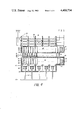
Turning first to FIG. 1, a CCD image sensor of the frame transfer type, generally designated 10, is shown. The image sensor includes: (1) an imaging array 12 comprising rows and columns of image sensing elements upon which an object 14 is imaged by a lens 16; (2) a frame storage array 18; and (3) an output shift register 20. The image sensor 10 is supplied with clock signals from a control circuit 22. In a frame transfer type image sensor, an imagewise charge pattern is accumulated in the image sensing array 12 during an exposure interval. The imagewise pattern of charge, consisting of rows and columns of charge packets, is then quickly shifted under the control of clock signals from the control circuit 22 into the frame storage array 18 in the direction of arrow A in FIG. 1. From the frame storage array, the charge pattern is read out one row at a time through the output shift register 20. A row of the imagewise charge pattern is transferred in parallel as indicated by arrow B into the output shift register, then the charge packets are shifted serially in the direction of arrow C to an output diode 24, forming the sampled video signal S. The timing and control of all the charge transfers are effected by clock signals from the control circuit 22. As noted above, a defect in the image sensor can give rise to the loss of an entire column of information. Such a defect is indicated schematically by an "X" in the frame storage array 18 in FIG. 1. The lost column of information is indicated by a vertical line 26 through the image.
The column defect compensating apparatus according to the present invention comprises an auxiliary shift register 28, containing signals representative of the locations of defective columns of the image sensor and a signal processing circuit 30 responsive to the signal from the output shift register 30 and the defect location signal from the auxiliary shift register 28 for compensating for the column defects. An example of such a signal processing circuit is shown as a sample and hold circuit 32. The sample and hold circuit 32 samples the output signal S from output shift register 20 each time a "no defect" signal is received from auxiliary shift register 28 indicating that there are no column defects. The "no defect" signals are represented as logical "one"s and the absence of a "no defect" signal is represented as a logical "0" in auxiliary shift register 28. This scheme has the effect of replacing the signal from a detective column with the signal from a neighboring nondefective column, since the output of the sample and hold circuit is not updated until the next nondefective signal is available from the output register. When the defect compensated signal is displayed, for example on a television monitor 32, the appearance of the column defect is suppressed.
Turning now to FIG. 2, one embodiment of the auxiliary shift register 28 according to the present invention, will be described in more detail. For purposes of description, a three-phase CCD is shown in FIG. 2, it being understood that one-, two-, or four-phase CCD's may also be employed with the present invention. The output shift register 20 and the last row of charge storage cells in the frame storage array of a frame transfer type image sensor are shown. The charge storage cells 34 are defined by channel stopping regions 36 and first-, second-, and third- phase electrodes 38, 40 and 42 respectively, supplied by three-phase clock signals P1, P2, P3 respectively. Output shift register 20 comprises a linear array of three phase electrodes 44, 46 and 48, supplied by three-phase clock signals Φ1, Φ2, and Φ3 respectively; an output gate 50; and an output diode 24. The auxiliary shift register 28 according to the present invention comprises a channel stopping diffusion 52 which defines an elongated channel adjacent the output shift register 20. A linear array of three-phase charge transfer electrodes 54, 56, and 58 are disposed over the channel area and are formed by extensions of the electrodes of the output shift register 20. An output gate 60 which is formed by an extension of output gate 50, and output diode 62, complete the auxiliary shift register.
An elongated input diode 64 is disposed adjacent the charge transfer cells of the auxiliary shift register, and disposed between each cell and the input diode 64 is an input gate 66 for controlling the introduction of signal charges from the input diode to the cells. Channel stopping diffusion 68 isolates the gates from each other. Each gate is connected to two input lines by a pair of connections 70 and 72 composed of final metal, i.e. the connecting lines are fabricated at the surface of the device for reasons to be explained later.
Connecting line 72 is connected to a clock input that is synchronous with clock signal P3. Connecting line 70 is connected to a constant voltage source V.
To program the auxiliary shift register the image sensor is operated and the output signal is displayed and observed to determine the location of the defective columns. For each defective column, the continuity of the connecting line 72 connecting the input gate of the corresponding cell of the auxiliary shift register to the P3 clock signal is destroyed by using well known laser apparatus of the type that is employed to trim thin film components such as resistors. Conversely, for each nondefective column, the continuity of the connecting line 70 connecting the input gate of a corresponding cell of the auxiliary shift register to fixed potential V is destroyed.
The operation of the auxiliary shift register will now be described with reference to FIG. 3. FIG. 3 is a potential diagram illustrating the potential profile in a cross section of the auxiliary shift register through the phase-1 electrode 54 taken along line 3--3 in FIG. 2.
Normally, the voltage on the input gate 66 is maintained so that a potential barrier indicated by dotted line 74 in FIG. 3 is formed between the input diode 64 and the potential well formed by the phase-1 electrode 54. To transfer charge from the input diode 64 to a cell of the auxiliary shift register 28, the voltage on the input gate 66 is temporarily changed to lower the potential barrier to the level denoted 74', thereby allowing charge to flow from the diode, over the barrier, into the cell of the shift register. All of the input gates supplied with the P3 signal through connecting line 72 behave in this manner, filling the cells of the auxiliary shift register with charge packets representing logical ones (1) each time a row of photocharge is transferred into the output shift register 20.
In contrast, the input gates that are supplied with signal via connecting line 70 are supplied with a constant potential V that maintains the potential barrier 78 high at all times, thereby preventing any charge from reaching the respective cells of the auxiliary shift register. These empty cells represent logical zeros (0) in the auxiliary shift register, indicating the presence of a defective column in the image sensing array.
In FIG. 2, a defect 76 (represented by a break in transfer gate 40, in the third column of the frame storage area) is illustrated. Defect 76 causes a loss of information in the third column of the sensor. The line 72' connecting the corresponding input gate of the third cell of the auxiliary shift register is shown broken, thereby causing a zero (0) to appear in the output of the shift register when the image sensor is operated. For all the other cells of the auxiliary shift register, the line 70 is broken, thereby causing a one (1) to appear in output of the shift register when the image sensor is operated.
An alternative configuration of the auxiliary shift register is shown in FIG. 4 wherein elements similar to those in FIG. 2 are similarly numbered. In this configuration, a separate input diode 64 is provided for each cell of the auxiliary shift register. All of the input diodes are connected to a diode bias potential by connecting lines 80, and the input gate 66 is continuous for the length of the shift register. The auxiliary shift register 28 is programmed by disrupting the continuity of line 80 to the appropriate input diodes, thereby disrupting the supply of charge carriers available for filling the corresponding cells of the shift register. In this example, only those lines where a logical zero (0) is desired in the shift register are disrupted, thereby decreasing the number of lines that need to be broken to program the auxiliary shift register. The device shown in FIG. 4 can be operated either by pulsing the diode bias in synchronism with the P3 signal, and keeping the potential of the input gate 66 constant thereby periodically spilling charge over the fixed barrier formed by input gate 66, or by pulsing the input gate 66 to periodically lower the potential barrier while keeping the diode bias constant.
The invention has been described with respect to preferred embodiments thereof, but it will be recognized that modifications and variations may be effected within the spirit and scope of the invention. For example, the invention has been described in terms of column defect compensating apparatus, however, the use of the word "column" herein is intended to be descriptive, but not limiting to one particular orientation of the image sensor.

Claims (3)

I claim:
1. Column defect compensating apparatus for a charge coupled device (CCD) image sensor of the type having a two-dimensional array comprising rows and columns of charge transfer elements, and an output CCD shift register arranged across one end of the columns and adapted to receive in parallel, one row of charge packets and to deliver the charge packets serially under control of clock signals to an output location, the column defect compensating apparatus comprising:
auxiliary CCD shift register means having a plurality of cells corresponding to the columns of the two-dimensional array for producing signals representing the condition of said columns;
means for applying said clock signals to said auxiliary shift register means to produce said condition representative signals in synchronism with the delivery of the charge packets in the output shift register to the output location;
programable input means for inserting, in parallel, into said auxiliary shift register, signals representing the condition of the columns of the array; said programable input means comprising (1) diode means disposed adjacent said cells of said auxiliary shift register for providing a source of signal charge, (2) gate means disposed between said diode means and said cells for selectively isolating said diode means from said cells, and (3) selectively destructible conductor means for controlling the transfer of charge from said diode means past said gate to said cells; and
signal processing circuit means responsive to the signals the said auxiliary shift register for compensating for the column defects in the output of the image sensor.
2. The invention claimed in claim 1 wherein said selectively destructible conductor means comprises a first conductor connected to said gate means and adapted to be connected to a fixed potential and a second conductor connected to said gate means and adapted to be connected to a clocking signal.
3. The invention claimed in claim 1 wherein said selectively destructible conductor means comprises conductor means connected to said diode.
US06/315,762 1981-10-28 1981-10-28 Column defect compensating apparatus for CCD image sensor Expired - Fee Related US4400734A (en)

Priority Applications (1)

Application Number Priority Date Filing Date Title
US06/315,762 US4400734A (en) 1981-10-28 1981-10-28 Column defect compensating apparatus for CCD image sensor

Applications Claiming Priority (1)

Application Number Priority Date Filing Date Title
US06/315,762 US4400734A (en) 1981-10-28 1981-10-28 Column defect compensating apparatus for CCD image sensor

Publications (1)

Publication Number Publication Date
US4400734A true US4400734A (en) 1983-08-23

Family

ID=23225949

Family Applications (1)

Application Number Title Priority Date Filing Date
US06/315,762 Expired - Fee Related US4400734A (en) 1981-10-28 1981-10-28 Column defect compensating apparatus for CCD image sensor

Country Status (1)

Country Link
US (1) US4400734A (en)

Cited By (12)

* Cited by examiner, † Cited by third party
Publication number Priority date Publication date Assignee Title
US4473845A (en) * 1983-01-24 1984-09-25 Eastman Kodak Company Method and apparatus for processing signals from a solid-state image sensor
DE3412889A1 (en) * 1983-04-08 1984-10-31 Citizen Watch Co., Ltd., Tokio/Tokyo IMAGE RECORDING SYSTEM
US4503460A (en) * 1982-02-26 1985-03-05 Siemens Aktiengesellschaft X-ray diagnostic installation comprising an image intensifier television chain
US4589028A (en) * 1983-11-29 1986-05-13 Fuji Photo Film Co., Ltd. Defect concealing image sensing device
US4644404A (en) * 1983-12-23 1987-02-17 Fuji Photo Film Co., Ltd. Solid-state image pickup device and manufacturing method thereof
US4785353A (en) * 1987-03-13 1988-11-15 Eastman Kodak Company Block readable video imager having noise compensation
US4893185A (en) * 1986-09-30 1990-01-09 Canon Kabushiki Kaisha Image sensing apparatus
US6671890B2 (en) * 2000-12-15 2004-01-06 San-Ei Faucet Mfg. Co., Ltd. Automatic water feed method in lavatory using artificial retina sensor and automatic water feed mechanism in lavatory using artificial retina sensor
US20040263649A1 (en) * 2003-05-15 2004-12-30 Keijirou Itakura Image defect correction apparatus and method
EP1921841A2 (en) * 1997-02-13 2008-05-14 FUJIFILM Corporation Monitoring method with a CCD imaging device and digital still camera using the same
US20150022175A1 (en) * 2013-07-18 2015-01-22 Springburo GmbH Voltage limiter and use of a voltage limiter to determine values of a power semiconductor element
US9191592B2 (en) 2012-02-29 2015-11-17 Apple Inc. Imaging sensor anomalous pixel column detection and calibration

Citations (4)

* Cited by examiner, † Cited by third party
Publication number Priority date Publication date Assignee Title
US4155121A (en) * 1978-06-30 1979-05-15 International Business Machines Corporation Redundant charge-coupled device and method
US4167754A (en) * 1977-01-28 1979-09-11 Sony Corporation Solid state television camera with noise eliminating circuit
US4179711A (en) * 1977-01-14 1979-12-18 Sony Corporation Defect noise compensating system
US4300163A (en) * 1978-12-08 1981-11-10 Matsushita Electric Industrial Co., Ltd. Solid-state imaging apparatus

Patent Citations (4)

* Cited by examiner, † Cited by third party
Publication number Priority date Publication date Assignee Title
US4179711A (en) * 1977-01-14 1979-12-18 Sony Corporation Defect noise compensating system
US4167754A (en) * 1977-01-28 1979-09-11 Sony Corporation Solid state television camera with noise eliminating circuit
US4155121A (en) * 1978-06-30 1979-05-15 International Business Machines Corporation Redundant charge-coupled device and method
US4300163A (en) * 1978-12-08 1981-11-10 Matsushita Electric Industrial Co., Ltd. Solid-state imaging apparatus

Non-Patent Citations (1)

* Cited by examiner, † Cited by third party
Title
"Charge Transfer Devices" by Sequin and Thompsett, Academic Press, 1975, p. 153. *

Cited By (14)

* Cited by examiner, † Cited by third party
Publication number Priority date Publication date Assignee Title
US4503460A (en) * 1982-02-26 1985-03-05 Siemens Aktiengesellschaft X-ray diagnostic installation comprising an image intensifier television chain
US4473845A (en) * 1983-01-24 1984-09-25 Eastman Kodak Company Method and apparatus for processing signals from a solid-state image sensor
DE3412889A1 (en) * 1983-04-08 1984-10-31 Citizen Watch Co., Ltd., Tokio/Tokyo IMAGE RECORDING SYSTEM
US4589028A (en) * 1983-11-29 1986-05-13 Fuji Photo Film Co., Ltd. Defect concealing image sensing device
US4644404A (en) * 1983-12-23 1987-02-17 Fuji Photo Film Co., Ltd. Solid-state image pickup device and manufacturing method thereof
US4893185A (en) * 1986-09-30 1990-01-09 Canon Kabushiki Kaisha Image sensing apparatus
US4785353A (en) * 1987-03-13 1988-11-15 Eastman Kodak Company Block readable video imager having noise compensation
EP1921841A2 (en) * 1997-02-13 2008-05-14 FUJIFILM Corporation Monitoring method with a CCD imaging device and digital still camera using the same
EP1921841A3 (en) * 1997-02-13 2011-07-20 FUJIFILM Corporation Monitoring method with a CCD imaging device and digital still camera using the same
US6671890B2 (en) * 2000-12-15 2004-01-06 San-Ei Faucet Mfg. Co., Ltd. Automatic water feed method in lavatory using artificial retina sensor and automatic water feed mechanism in lavatory using artificial retina sensor
US20040263649A1 (en) * 2003-05-15 2004-12-30 Keijirou Itakura Image defect correction apparatus and method
US7483063B2 (en) * 2003-05-15 2009-01-27 Panasonic Corporation Image defect correction apparatus and method
US9191592B2 (en) 2012-02-29 2015-11-17 Apple Inc. Imaging sensor anomalous pixel column detection and calibration
US20150022175A1 (en) * 2013-07-18 2015-01-22 Springburo GmbH Voltage limiter and use of a voltage limiter to determine values of a power semiconductor element

Similar Documents

Publication Publication Date Title
US4322752A (en) Fast frame rate sensor readout
US4555732A (en) Image sensor correction system
US4380755A (en) Monolithically integrated two-dimensional image sensor with a difference forming stage
KR100614720B1 (en) Active pixel sensor with shared row timing signals
US4167754A (en) Solid state television camera with noise eliminating circuit
KR100750778B1 (en) Photodiode active pixel sensor with shared reset signal row select
US5430481A (en) Multimode frame transfer image sensor
US4400734A (en) Column defect compensating apparatus for CCD image sensor
JP2000125203A (en) Amplifier solid-state image pickup device and its drive method
US5134489A (en) X-Y addressable solid state imager for low noise operation
US5134488A (en) X-Y addressable imager with variable integration
EP0748112B1 (en) Solid state image sensor device and its driving method
US4654714A (en) Pixel addressing system
US3983395A (en) MIS structures for background rejection in infrared imaging devices
US4263620A (en) Picture pickup target and reading device assembly
JPS61111078A (en) Method for correcting defect of video output signal and image sensor device using it's method
US4626916A (en) Solid state image pickup device
US4831451A (en) Horizontal scanner for image sensor arrays
KR100742439B1 (en) Improved digital imaging circuit and method
KR20010070481A (en) Active pixel sensor with improved reference signal
JPS639358A (en) Original reader
US5168379A (en) Solid state imaging device having a defect relief system
US6624849B1 (en) Solid-state imaging apparatus for motion detection
JP2910485B2 (en) Image reading apparatus and image reading method
US4577232A (en) Line addressed charge coupled imager

Legal Events

Date Code Title Description
AS Assignment

Owner name: EASTMAN KODAK COMPANY, ROCHESTER, NY A NJ CORP.

Free format text: ASSIGNMENT OF ASSIGNORS INTEREST.;ASSIGNOR:DAVY, LEE N.;REEL/FRAME:004116/0707

Effective date: 19811016

MAFP Maintenance fee payment

Free format text: PAYMENT OF MAINTENANCE FEE, 4TH YEAR, PL 96-517 (ORIGINAL EVENT CODE: M170); ENTITY STATUS OF PATENT OWNER: LARGE ENTITY

Year of fee payment: 4

FEPP Fee payment procedure

Free format text: PAYOR NUMBER ASSIGNED (ORIGINAL EVENT CODE: ASPN); ENTITY STATUS OF PATENT OWNER: LARGE ENTITY

FEPP Fee payment procedure

Free format text: MAINTENANCE FEE REMINDER MAILED (ORIGINAL EVENT CODE: REM.); ENTITY STATUS OF PATENT OWNER: LARGE ENTITY

LAPS Lapse for failure to pay maintenance fees
STCH Information on status: patent discontinuation

Free format text: PATENT EXPIRED DUE TO NONPAYMENT OF MAINTENANCE FEES UNDER 37 CFR 1.362

FP Lapsed due to failure to pay maintenance fee

Effective date: 19910825