US4420874A - Method of producing an IIL semiconductor device utilizing self-aligned thickened oxide patterns - Google Patents
Method of producing an IIL semiconductor device utilizing self-aligned thickened oxide patterns Download PDFInfo
- Publication number
- US4420874A US4420874A US06/340,286 US34028682A US4420874A US 4420874 A US4420874 A US 4420874A US 34028682 A US34028682 A US 34028682A US 4420874 A US4420874 A US 4420874A
- Authority
- US
- United States
- Prior art keywords
- regions
- insulating layer
- forming
- layer
- conductivity type
- Prior art date
- Legal status (The legal status is an assumption and is not a legal conclusion. Google has not performed a legal analysis and makes no representation as to the accuracy of the status listed.)
- Expired - Fee Related
Links
Images


Classifications
-
- H—ELECTRICITY
- H01—ELECTRIC ELEMENTS
- H01L—SEMICONDUCTOR DEVICES NOT COVERED BY CLASS H10
- H01L27/00—Devices consisting of a plurality of semiconductor or other solid-state components formed in or on a common substrate
- H01L27/02—Devices consisting of a plurality of semiconductor or other solid-state components formed in or on a common substrate including semiconductor components specially adapted for rectifying, oscillating, amplifying or switching and having at least one potential-jump barrier or surface barrier; including integrated passive circuit elements with at least one potential-jump barrier or surface barrier
- H01L27/0203—Particular design considerations for integrated circuits
- H01L27/0214—Particular design considerations for integrated circuits for internal polarisation, e.g. I2L
- H01L27/0229—Particular design considerations for integrated circuits for internal polarisation, e.g. I2L of bipolar structures
- H01L27/0233—Integrated injection logic structures [I2L]
-
- G—PHYSICS
- G11—INFORMATION STORAGE
- G11C—STATIC STORES
- G11C11/00—Digital stores characterised by the use of particular electric or magnetic storage elements; Storage elements therefor
- G11C11/21—Digital stores characterised by the use of particular electric or magnetic storage elements; Storage elements therefor using electric elements
- G11C11/34—Digital stores characterised by the use of particular electric or magnetic storage elements; Storage elements therefor using electric elements using semiconductor devices
- G11C11/40—Digital stores characterised by the use of particular electric or magnetic storage elements; Storage elements therefor using electric elements using semiconductor devices using transistors
- G11C11/41—Digital stores characterised by the use of particular electric or magnetic storage elements; Storage elements therefor using electric elements using semiconductor devices using transistors forming static cells with positive feedback, i.e. cells not needing refreshing or charge regeneration, e.g. bistable multivibrator or Schmitt trigger
- G11C11/411—Digital stores characterised by the use of particular electric or magnetic storage elements; Storage elements therefor using electric elements using semiconductor devices using transistors forming static cells with positive feedback, i.e. cells not needing refreshing or charge regeneration, e.g. bistable multivibrator or Schmitt trigger using bipolar transistors only
- G11C11/4113—Digital stores characterised by the use of particular electric or magnetic storage elements; Storage elements therefor using electric elements using semiconductor devices using transistors forming static cells with positive feedback, i.e. cells not needing refreshing or charge regeneration, e.g. bistable multivibrator or Schmitt trigger using bipolar transistors only with at least one cell access to base or collector of at least one of said transistors, e.g. via access diodes, access transistors
-
- H—ELECTRICITY
- H01—ELECTRIC ELEMENTS
- H01L—SEMICONDUCTOR DEVICES NOT COVERED BY CLASS H10
- H01L21/00—Processes or apparatus adapted for the manufacture or treatment of semiconductor or solid state devices or of parts thereof
- H01L21/70—Manufacture or treatment of devices consisting of a plurality of solid state components formed in or on a common substrate or of parts thereof; Manufacture of integrated circuit devices or of parts thereof
- H01L21/71—Manufacture of specific parts of devices defined in group H01L21/70
- H01L21/76—Making of isolation regions between components
- H01L21/762—Dielectric regions, e.g. EPIC dielectric isolation, LOCOS; Trench refilling techniques, SOI technology, use of channel stoppers
- H01L21/76202—Dielectric regions, e.g. EPIC dielectric isolation, LOCOS; Trench refilling techniques, SOI technology, use of channel stoppers using a local oxidation of silicon, e.g. LOCOS, SWAMI, SILO
-
- H—ELECTRICITY
- H01—ELECTRIC ELEMENTS
- H01L—SEMICONDUCTOR DEVICES NOT COVERED BY CLASS H10
- H01L21/00—Processes or apparatus adapted for the manufacture or treatment of semiconductor or solid state devices or of parts thereof
- H01L21/70—Manufacture or treatment of devices consisting of a plurality of solid state components formed in or on a common substrate or of parts thereof; Manufacture of integrated circuit devices or of parts thereof
- H01L21/71—Manufacture of specific parts of devices defined in group H01L21/70
- H01L21/76—Making of isolation regions between components
- H01L21/763—Polycrystalline semiconductor regions
Definitions
- the present invention relates to an integrated injection logic (I 2 L) type semiconductor device and a method of producing the same.
- I 2 L type semiconductor memory device in accordance with the present invention is used for a bipolar static random access memory (RAM) device, a logic circuit or the like.
- RAM static random access memory
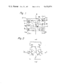
- FIGS. 1, 2, 3 and 4 Prior art memory cells of the I 2 L type memory devices are illustrated in FIGS. 1, 2, 3 and 4.
- FIGS. 1 and 2 illustrate an npn coupled type memory cell
- FIGS. 3 and 4 illustrate a pnp coupled type memory cell
- FIGS. 1 and 3 illustrate the structure of the memory cells
- FIGS. 2 and 4 illustrate the circuit diagrams of the memory cells.
- a p + type injector region J a contact portion J w of said p + type injector region, p + type base regions B, contact portions B 0 and B 1 of said p + type base regions, n + type collector regions C(n + ), contact portions C h0 , C h1 , C s0 and C s1 of said n + type collector regions, writing-in or reading-out lines D 0 and D 1 , and a word line W are illustrated.
- An opposite word line W- connected to the semiconductor body is not shown in FIG. 1. As illustrated in FIGS.
- the PNP type transistors Q 2 and Q 3 are constituted by lateral bipolar transistors, each of which transistors comprises a, p type injector region J as an emitter, an n type region N B as a base and p type regions B as collectors.
- the NPN type transistors Q 0 and Q 1 are constituted by vertical bipolar transistors, each of which transistors comprises an n type region C(n + ) as a collector, a p type base region B as a base and an n type region N B , which is located under the base region B, as an emitter.
- both the PNP type transistors Q 2 and Q 3 and the NPN type transistors Q 0 and Q 1 have the n type region N B as a common connecting body.
- a p + type injector region J a contact portion J w of said p + type injector region, p + type base regions B, contact portions B 0 and B 1 of said p + type base regions, n + type collector regions C(n + ), contact portions C h0 and C h1 of said n + type collector regions, contact portions C' s0 and C' s1 of emitter regions E(p+) of a lateral pnp transistor for detection, writing-in or reading-out lines D 0 and D 1 , and a word line W are illustrated.
- An opposite word line W - is connected to the semiconductor body and is not shown in FIG. 3. As illustrated in FIGS.
- the PNP type transistors Q 2 and Q 3 are constituted by lateral bipolar transistors, each of which transistors comprises a p type injector region J as a common emitter, an n type region N B as a, base and p type regions B as collectors.
- the NPN type transistors Q 0 and Q 1 are constituted by vertical bipolar transistors, each of which transistors comprises an n type region C(n + ) as a collector, a p type base region B as a base and the n type region N B , which is located under the base region B, as an emitter.
- the PNP type transistors Q 4 and Q 5 are constituted by lateral bipolar transistors, each of which transistors comprises a p type region B as a collector, an n type region N BD connected to the n type region B as a base and a p + type region E(P+) as an emitter.
- all of the PNP type transistors Q 2 and Q 3 , NPN type transistors Q 0 and Q 1 and the PNP type transistors Q 4 and Q 5 have the n type regions N B and N BD as a common connecting body.
- B 0 , C h0 , C s0 and D 0 are related to the "0" (or “1") side transistor Q 0
- B 1 , C h1 , C s1 and D 1 are related to the "1" (or “0") side transistor Q 1 .
- I 2 L memory cell is described in, for example, "Injection-coupled Memory: A High-Density Static Bipolar Memory” by S. K. Wiedmann, IEEE Journal of Solid-state Circuits, Vol. SC-8, No. 5, October 1973, and in the Japanese Patent Application No. 51-71855 entitled "A Semiconductor Memory Device".
- the present invention has been proposed in order to solve the problems in the prior art semiconductor memory devices set forth above.
- a semiconductor memory device having an elementary region which is isolated by V-shape grooves from the other portions of the device, said semiconductor memory device comprising an insulation coating covering the surface of the semiconductor body of the device, predetermined portions of said insulation coating being thicker and said thicker insulating layers surrounding the central portion of said elementary region, an injector region formed under said insulating layer and surrounded by said thicker portions of said insulating layer, and base regions formed under said insulating layer between said thicker portions of said insulating layer and said V-shape grooves.
- FIG. 1 illustrates the structure of a prior art I 2 L type memory cell of an npn coupled type
- FIG. 2 illustrates the circuit diagram of the device of FIG. 1
- FIG. 3 illustrates the structure of a prior art I 2 L type memory cell of a pnp coupled type
- FIG. 4 illustrates the circuit diagram of the device of FIG. 3,
- FIGS. 5A through 15D illustrate a process of manufacturing I 2 L type memory cells in accordance with an embodiment of the present invention, in which
- FIGS. 5A, 6A, 7A, 8A, 9A, 10A, 11A, 12A, 13A, 14A and 15A illustrate the plan views of the device in the steps of the manufacturing process
- FIGS. 5B, 6B, 7B, 8B, 9B, 10B, 11B, 12B, 13B, 14B and 15B illustrate the cross-sectional views of the device taken along the lines b--b in FIGS. 5A through 15A, respectively,
- FIGS. 5C, 6C, 7C, 8C, 9C, 10C, 11C, 12C, 13C, 14C and 15C illustrate the cross-sectional views of the device taken along the lines c--c in FIGS. 5A through 15A, respectively, and
- FIGS. 5D, 6D, 7D, 8D, 9D, 10D, 11D, 12D, 13D, 14D and 15D illustrate the cross-sectional views of the device taken along the lines d--d in FIGS. 5A through 15A, respectively.
- FIGS. 5A through 15D A process of manufacturing an I 2 L type semiconductor memory device in accordance with an embodiment of the present invention will now be described with reference to FIGS. 5A through 15D.
- an n + type layer 2 is formed in a p type silicon (Si) semiconductor substrate 1 having the Miller indices of (100) by introducing n type impurities by means of a gaseous diffusion process or an ion implantation process.
- n type layer 3 of approximately 2 ⁇ m is formed by means of, for example, the gaseous epitaxial growth process.
- the n type layer 3 has also the Miller indices of (100).
- a silicon dioxide (SiO 2 ) layer 4 with a thickness of approximately 1400 ⁇ is formed by means of for example, thermal oxidation process.
- a silicon nitride (Si 3 N 4 ) layer 5 with a thickness of approximately 2500 ⁇ is formed by means of, for example, the chemical vaper deposition process.
- This silicon nitride layer 5 acts as an anti-oxidation mask.
- a patterning of the silicon nitride layer 5 is effected by using, for example, the photolithographic process, so that a masking pattern is formed which covers the portion of the n type layer 3 where base regions 91, 92 and an injector region 10 (FIG. 10B) are to be formed.
- a photoresist layer 6 is applied to protect the portion of silicon dioxide layer 4 covering at least a portion of the surface of the n type region located between the base regions 91, 92 and the injector region 10, and a selective removal of the silicon dioxide layer 4 is effected by using the masking pattern of the silicon nitride layer 5 and the photoresist layer 6.
- an etching of the n type layer 3 is effected by using the masking pattern of the silicon nitride layer 5 and the silicon dioxide layer 4, so that V-shape grooves 71, 72, 73, 74, 75, 76 and 77 which define the boundary of elementary regions of the device are formed.
- an anisotropic etching solution with which the rate of the etching is greater for the plane having the Miller indices of (100) than for the other planes, is used.
- a solution containing, for example, potassium hydroxide (KOH) as the main constituent is used.
- the depth of the V-shape grooves 71, 72, 73, 74 and 75 in the regions I, II, III and IV of FIG. 7A does not extend to the boundaries of where the n type layer 3 and the n + type layer 2 meet, due to the selection of the width of the V-shape groove at the surface of the n type layer 3, as illustrated in FIGS. 7B and 7C.
- the depth of the V-shape grooves 76 and 77 in the regions V and VI of FIG. 7A extends through the n + type layer 2 due to the selection of the width of the V-shape groove at the surface of the n type layer 3, as illustrated in FIG. 7D.
- a silicon dioxide layer 16 is formed on the inner surface the V-shape grooves 71, 72, 73, 74, 75, 76 and 77 by means of, for example, a thermal oxidation process.
- the thickness of the silicon dioxide layer 16 is approximately 3000 ⁇ to 5000 ⁇ .
- the thickness of the portions of the silicon dioxide layer 4 which are not covered by a silicon nitride layer and not occupied by V-shape grooves is increased.
- a polycrystalline silicon layer is formed on the silicon dioxide layer and silicon nitride layer by means of, for example, chemical vaper deposition process, and then said polycrystalline silicon layer is polished chemically and mechanically by using a polishing solution containing potassium hydroxide and aluminum oxide (Al 2 O 3 ) as the main constituents.
- This polishing is completed when the silicon nitride layer 5 reveals itself from said polycrystalline silicon layer which is being polished, so that the polycrystalline silicon layers 81, 82, 83, 84, 85, 86 and 87 are maintained only in the V-shape grooves 71, 72, 73, 74, 75, 76 and 77, as illustrated in FIGS. 8B, 8C and 8D.
- silicon dioxide layers 41 are formed on the surfaces of the polycrystalline silicon layers 81, 82, 83, 84, 85, 86 and 87 and the thickness of the portions of the silicon dioxide layer 4 which are not covered by the silicon nitride layer 5 are enlarged by using the thermal oxidation process.
- the thicker portions 42 of the silicon dioxide layer 4 are illustrated in FIGS. 9B and 9D.
- the silicon dioxide layer 42 has a thickness of approximately 7000 ⁇ to 12000 ⁇ . Then, the silicon nitride layer 5 is removed.
- p type base regions 91 and 92 and a p type injector region 10 are formed by introducing, for example, boron (B) by means of, for example, the ion implantation process. It is also possible to form these p type base regions and a p type injector region below the thin portions of the silicon dioxide layer by applying, for example, the solid to solid diffusion process for a long duration.
- FIGS. 10A, 10B and 10C P type base regions 91', 92' of the adjacent memory cells on the same word line are illustrated in FIGS. 10A, 10B and 10C.
- Base regions 91", 92" of the memory cells on the adjacent word lines are illustrated in FIG. 10D.
- n type emitter regions 111 h , 111 s , 112 h and 112 s are formed in the base regions 91 and 92 by introducing n type impurities for example, arsenic (As) or phosphorus (P), by means of an ion implantation process or a gaseous diffusion process with a masking pattern. Said gaseous diffusion is effected through windows which are formed in the silicon dioxide layer 4 by means of a patterning process with a masking pattern.
- the emitter regions 111 h and 112 h constitute HOLD side emitters, while the emitter regions 111 s and 112 s constitute SELECT side emitters.
- windows 17 for providing conduction paths to electrodes are formed in the silicon dioxide layer 4 by means of the patterning process with the photolithographic process.
- an aluminum (Al) layer with a thickness of approximately 1000 to 3000 ⁇ is deposited on the surface of the device by means of, for example, the vapor deposition process, and then electrode conductors 121 and 122 of a first wiring layer are formed by means of the patterning process with a photolithographic process applied to said aluminum layers. These electrode conductors 121 and 122 do not need to be exposed on the surface of the device. These electrode conductors 121 and 122 correspond to the cross coupling conductors connecting the bases of the transistors Q 0 and Q 1 to the collectors of the transistors Q 2 and Q 3 , respectively, in the prior art devices of FIGS. 2 and 4.
- aluminum oxide (Al 2 O 3 ) layers 131 and 132 are formed on the electrode conductors 121 and 122 by means of an anodic oxidation process in which, for example, a solution of ammonium borate is used with a voltage of 100 V.
- the aluminum oxide layer has a thickness of approximately 200 to 500 ⁇ .
- Silicon dioxide layers, which were formed on the windows in which no conductors are filled, are removed from the portions 18 by means of, for example, the washing process.
- an aluminum layer with a thickness of approximately 8000 to 12000 ⁇ is deposited on the surface of the device by means of, for example, a vapor deposition process, and then electrode conductors 141, 142, of a second wiring layer are formed by means of the patterning process with the photolithographic process applied to said aluminum layer.
- the electrode conductors 141 and 142 constitute digit lines connected to the SELECT side emitter regions 111 s and 112 s .
- Electrode conductors 141 and 142 are arranged on the cross coupling conductors 121 and 122.
- the oxide layers 131 and 132 on the cross coupling conductors 121 and 122 prevent a short circuit between the cross coupling conductors 121 and 122 and the electrode conductors 141 and 142.
- an insulating layer 151 is formed to cover the electrode conductors and the exposed insulating layer.
- the insulating layer 151 of, for example, phosphosilicate glass is formed by, for example, a chemical vapor deposition process with thickness of approximately 8000 to 10000 ⁇ .
- a window is formed in the insulating layer 151 corresponding to the position 18 by means of an ordinary photolithographical process.
- an aluminum layer with a thickness of approximately 8000 to 12000 ⁇ is deposited on the surface of the insulating layer 151 by means of, for example, a vapor deposition process.
- an electrode conductor 15 of third wiring layers are formed by means of the patterning process with the photolithographic process applied to the aluminum layer.
- the electrode conductor 15 constitutes a word line. Sufficient widths and reduced resistivity are obtained in the above described structures of the wiring. Accordingly, the speed of the I 2 L memory device can be increased.
- a passivation is effected by coating the surface of the memory cell array with a layer of phosphosilicate glass and the like, though such a layer is not illustrated in the drawings.
- the ordinary V-shape grooves 71, 72, 73, 74 and 75 prevent parasitic pnp effects which might occur between the adjacent base regions in a memory cell or between the adjacent memory cells having the same opposite word line (W - ) mentioned above.
- the locations of the base regions 91 and 92 and the injector region 10 in the structure of FIGS. 15A, 15B, 15C and 15D have been determined by the patterning of the silicon nitride layer 5 in the structure of FIGS. 5A, 5B, 5C and 5D, because the locations of the V-shape grooves 71, 72, 73, 74, 75, 76 and 77 and the thicker portions 42 in the structure of FIGS. 9B, 9C and 9D have been determined by the patterning of the silicon nitride layer 5 in the structure of FIGS. 5A, 5B, 5C and 5D. Accordingly, in accordance with the process illustrated in FIGS.
- the injector region and the base regions are formed in the manner of so-called "self-alignment". This makes it possible to reduce the size of the device and increase the degree of integration of the integrated circuit of the device. Also, in accordance with the process illustrated in FIGS. 5A through 15D, the electrode conductors of the second wiring layer can be formed on the portion in which the electrode conductors of the first wiring layer are buried. This also makes it possible to increase the degree of integration of the integrated circuit of the device.
- a control circuit such as an address decoder and the like for controlling said I 2 L memory cell can also be formed on the semiconductor body on which said I 2 L memory cell is formed.
- Circuits such as a bipolar transistor logic circuit, an I 2 l logic circuit and the like for forming said control circuit can have the above described V-shape groove structure as a means for isolating the circuit elements.
- the structure and the process of the production of an I 2 L memory cell described above can be applied not only to an I 2 L memory cell but also to semiconductor devices including the I 2 L memory cell.
Abstract
An I2 L type semiconductor device having an elementary region which is isolated by V-shape grooves from the other portions of the device, said semiconductor device comprising an insulating layer coating covering the surface of the semiconductor body of the device, wherein an injector region is formed under said insulating layer and surrounded by thicker portions of said insulating layer, and base regions are formed under said insulating layer between said thicker portions of said insulating layer and said V-shape grooves.
Description
This is a division of application Ser. No. 105,152 filed Dec. 19, 1979 now Pat. No. 4,375,645.
The present invention relates to an integrated injection logic (I2 L) type semiconductor device and a method of producing the same. The I2 L type semiconductor memory device in accordance with the present invention is used for a bipolar static random access memory (RAM) device, a logic circuit or the like.
Prior art memory cells of the I2 L type memory devices are illustrated in FIGS. 1, 2, 3 and 4. FIGS. 1 and 2 illustrate an npn coupled type memory cell, while FIGS. 3 and 4 illustrate a pnp coupled type memory cell. FIGS. 1 and 3 illustrate the structure of the memory cells, while FIGS. 2 and 4 illustrate the circuit diagrams of the memory cells.
In FIG. 1, a p+ type injector region J, a contact portion Jw of said p+ type injector region, p+ type base regions B, contact portions B0 and B1 of said p+ type base regions, n+ type collector regions C(n+), contact portions Ch0, Ch1, Cs0 and Cs1 of said n+ type collector regions, writing-in or reading-out lines D0 and D1, and a word line W are illustrated. An opposite word line W- connected to the semiconductor body is not shown in FIG. 1. As illustrated in FIGS. 1 and 2, the PNP type transistors Q2 and Q3 are constituted by lateral bipolar transistors, each of which transistors comprises a, p type injector region J as an emitter, an n type region NB as a base and p type regions B as collectors. The NPN type transistors Q0 and Q1 are constituted by vertical bipolar transistors, each of which transistors comprises an n type region C(n+) as a collector, a p type base region B as a base and an n type region NB, which is located under the base region B, as an emitter. Thus, both the PNP type transistors Q2 and Q3 and the NPN type transistors Q0 and Q1 have the n type region NB as a common connecting body.
In FIG. 3, a p+ type injector region J, a contact portion Jw of said p+ type injector region, p+ type base regions B, contact portions B0 and B1 of said p+ type base regions, n+ type collector regions C(n+), contact portions Ch0 and Ch1 of said n+ type collector regions, contact portions C's0 and C's1 of emitter regions E(p+) of a lateral pnp transistor for detection, writing-in or reading-out lines D0 and D1, and a word line W are illustrated. An opposite word line W- is connected to the semiconductor body and is not shown in FIG. 3. As illustrated in FIGS. 3 and 4, the PNP type transistors Q2 and Q3 are constituted by lateral bipolar transistors, each of which transistors comprises a p type injector region J as a common emitter, an n type region NB as a, base and p type regions B as collectors. The NPN type transistors Q0 and Q1 are constituted by vertical bipolar transistors, each of which transistors comprises an n type region C(n+) as a collector, a p type base region B as a base and the n type region NB, which is located under the base region B, as an emitter. The PNP type transistors Q4 and Q5 are constituted by lateral bipolar transistors, each of which transistors comprises a p type region B as a collector, an n type region NBD connected to the n type region B as a base and a p+ type region E(P+) as an emitter. Thus, all of the PNP type transistors Q2 and Q3, NPN type transistors Q0 and Q1 and the PNP type transistors Q4 and Q5 have the n type regions NB and NBD as a common connecting body.
In FIGS. 1, 2, 3 and 4, B0, Ch0, Cs0 and D0 are related to the "0" (or "1") side transistor Q0, while B1, Ch1, Cs1 and D1 are related to the "1" (or "0") side transistor Q1.
In the memory cell of FIGS. 1 and 3, since the structures of the transistors Q0 and Q1 of the flip-flop circuit are symmetrical, the operations of the transistors Q0 and Q1 of the flip-flop circuit are symmetrical. Accordingly the currents which energize the transistors Q0 and Q1 are caused to be precisely symmetrical, and no asymmetry in the operations of the writing-in and the reading-out of information occurs. Also, since the currents delivered from the injector region J are uniform in every direction, high injection efficiency is obtained and, accordingly, excellent operating characteristics of the flip-flop circuit are obtained.
However, in the manufacture of the memory cell of FIGS. 1 and 3 it is necessary to use a masking pattern which defines an opening in the insulation layer over the p+ type injector region through which an electrical connection between the p+ type injector and the conductor is formed. In order to avoid misalignment of the mask, it is necessary to make the size of the device large. Also, conductors for internal connections of the device occupy a predetermined volume of space in the device.
Therefore, in the prior art, it was difficult to reduce the size of an I2 L type memory device.
The prior art I2 L memory cell is described in, for example, "Injection-coupled Memory: A High-Density Static Bipolar Memory" by S. K. Wiedmann, IEEE Journal of Solid-state Circuits, Vol. SC-8, No. 5, October 1973, and in the Japanese Patent Application No. 51-71855 entitled "A Semiconductor Memory Device".
The present invention has been proposed in order to solve the problems in the prior art semiconductor memory devices set forth above.
It is the principal object of the present invention to reduce the size of an I2 L type memory device and increase the degree of integration of an integrated circuit for an I2 L type memory device.
In accordance with the present invention, a semiconductor memory device is provided having an elementary region which is isolated by V-shape grooves from the other portions of the device, said semiconductor memory device comprising an insulation coating covering the surface of the semiconductor body of the device, predetermined portions of said insulation coating being thicker and said thicker insulating layers surrounding the central portion of said elementary region, an injector region formed under said insulating layer and surrounded by said thicker portions of said insulating layer, and base regions formed under said insulating layer between said thicker portions of said insulating layer and said V-shape grooves.
FIG. 1 illustrates the structure of a prior art I2 L type memory cell of an npn coupled type,
FIG. 2 illustrates the circuit diagram of the device of FIG. 1,
FIG. 3 illustrates the structure of a prior art I2 L type memory cell of a pnp coupled type,
FIG. 4 illustrates the circuit diagram of the device of FIG. 3,
FIGS. 5A through 15D illustrate a process of manufacturing I2 L type memory cells in accordance with an embodiment of the present invention, in which
FIGS. 5A, 6A, 7A, 8A, 9A, 10A, 11A, 12A, 13A, 14A and 15A illustrate the plan views of the device in the steps of the manufacturing process,
FIGS. 5B, 6B, 7B, 8B, 9B, 10B, 11B, 12B, 13B, 14B and 15B illustrate the cross-sectional views of the device taken along the lines b--b in FIGS. 5A through 15A, respectively,
FIGS. 5C, 6C, 7C, 8C, 9C, 10C, 11C, 12C, 13C, 14C and 15C illustrate the cross-sectional views of the device taken along the lines c--c in FIGS. 5A through 15A, respectively, and
FIGS. 5D, 6D, 7D, 8D, 9D, 10D, 11D, 12D, 13D, 14D and 15D illustrate the cross-sectional views of the device taken along the lines d--d in FIGS. 5A through 15A, respectively.
A process of manufacturing an I2 L type semiconductor memory device in accordance with an embodiment of the present invention will now be described with reference to FIGS. 5A through 15D.
As illustrated in FIGS. 5A, 5B, 5C and 5D, an n+ type layer 2 is formed in a p type silicon (Si) semiconductor substrate 1 having the Miller indices of (100) by introducing n type impurities by means of a gaseous diffusion process or an ion implantation process.
Then, an n type layer 3 of approximately 2 μm is formed by means of, for example, the gaseous epitaxial growth process. The n type layer 3 has also the Miller indices of (100).
Then, a silicon dioxide (SiO2) layer 4 with a thickness of approximately 1400 Å is formed by means of for example, thermal oxidation process.
Then, a silicon nitride (Si3 N4) layer 5 with a thickness of approximately 2500 Å is formed by means of, for example, the chemical vaper deposition process. This silicon nitride layer 5 acts as an anti-oxidation mask.
Then, a patterning of the silicon nitride layer 5 is effected by using, for example, the photolithographic process, so that a masking pattern is formed which covers the portion of the n type layer 3 where base regions 91, 92 and an injector region 10 (FIG. 10B) are to be formed.
As illustrated in FIGS. 6A, 6B, 6C and 6D, a photoresist layer 6 is applied to protect the portion of silicon dioxide layer 4 covering at least a portion of the surface of the n type region located between the base regions 91, 92 and the injector region 10, and a selective removal of the silicon dioxide layer 4 is effected by using the masking pattern of the silicon nitride layer 5 and the photoresist layer 6.
As illustrated in FIGS. 7A, 7B, 7C and 7D, after removing the photoresist layer 6, an etching of the n type layer 3 is effected by using the masking pattern of the silicon nitride layer 5 and the silicon dioxide layer 4, so that V- shape grooves 71, 72, 73, 74, 75, 76 and 77 which define the boundary of elementary regions of the device are formed. In this etching process, an anisotropic etching solution, with which the rate of the etching is greater for the plane having the Miller indices of (100) than for the other planes, is used. For this anisotropic etching solution, a solution containing, for example, potassium hydroxide (KOH) as the main constituent is used. The depth of the V- shape grooves 71, 72, 73, 74 and 75 in the regions I, II, III and IV of FIG. 7A does not extend to the boundaries of where the n type layer 3 and the n+ type layer 2 meet, due to the selection of the width of the V-shape groove at the surface of the n type layer 3, as illustrated in FIGS. 7B and 7C. However, the depth of the V- shape grooves 76 and 77 in the regions V and VI of FIG. 7A extends through the n+ type layer 2 due to the selection of the width of the V-shape groove at the surface of the n type layer 3, as illustrated in FIG. 7D.
As illustrated in FIGS. 8A, 8B, 8C and 8D, a silicon dioxide layer 16 is formed on the inner surface the V- shape grooves 71, 72, 73, 74, 75, 76 and 77 by means of, for example, a thermal oxidation process. The thickness of the silicon dioxide layer 16 is approximately 3000 Å to 5000 Å. At the same time, the thickness of the portions of the silicon dioxide layer 4 which are not covered by a silicon nitride layer and not occupied by V-shape grooves is increased. Then, a polycrystalline silicon layer is formed on the silicon dioxide layer and silicon nitride layer by means of, for example, chemical vaper deposition process, and then said polycrystalline silicon layer is polished chemically and mechanically by using a polishing solution containing potassium hydroxide and aluminum oxide (Al2 O3) as the main constituents. This polishing is completed when the silicon nitride layer 5 reveals itself from said polycrystalline silicon layer which is being polished, so that the polycrystalline silicon layers 81, 82, 83, 84, 85, 86 and 87 are maintained only in the V- shape grooves 71, 72, 73, 74, 75, 76 and 77, as illustrated in FIGS. 8B, 8C and 8D.
As illustrated in FIGS. 9A, 9B, 9C and 9D, silicon dioxide layers 41 are formed on the surfaces of the polycrystalline silicon layers 81, 82, 83, 84, 85, 86 and 87 and the thickness of the portions of the silicon dioxide layer 4 which are not covered by the silicon nitride layer 5 are enlarged by using the thermal oxidation process. The thicker portions 42 of the silicon dioxide layer 4 are illustrated in FIGS. 9B and 9D. The silicon dioxide layer 42 has a thickness of approximately 7000 Å to 12000Å. Then, the silicon nitride layer 5 is removed.
As illustrated in FIGS. 10A, 10B, 10C and 10D, p type base regions 91 and 92 and a p type injector region 10 are formed by introducing, for example, boron (B) by means of, for example, the ion implantation process. It is also possible to form these p type base regions and a p type injector region below the thin portions of the silicon dioxide layer by applying, for example, the solid to solid diffusion process for a long duration.
P type base regions 91', 92' of the adjacent memory cells on the same word line are illustrated in FIGS. 10A, 10B and 10C. Base regions 91", 92" of the memory cells on the adjacent word lines are illustrated in FIG. 10D.
As illustrated in FIGS. 11A, 11B, 11C and 11D, n type emitter regions 111h, 111s, 112h and 112s are formed in the base regions 91 and 92 by introducing n type impurities for example, arsenic (As) or phosphorus (P), by means of an ion implantation process or a gaseous diffusion process with a masking pattern. Said gaseous diffusion is effected through windows which are formed in the silicon dioxide layer 4 by means of a patterning process with a masking pattern. The emitter regions 111h and 112h constitute HOLD side emitters, while the emitter regions 111s and 112s constitute SELECT side emitters. Then windows 17 for providing conduction paths to electrodes are formed in the silicon dioxide layer 4 by means of the patterning process with the photolithographic process.
As illustrated in FIGS. 12A, 12B, 12C and 12D, an aluminum (Al) layer with a thickness of approximately 1000 to 3000 Å is deposited on the surface of the device by means of, for example, the vapor deposition process, and then electrode conductors 121 and 122 of a first wiring layer are formed by means of the patterning process with a photolithographic process applied to said aluminum layers. These electrode conductors 121 and 122 do not need to be exposed on the surface of the device. These electrode conductors 121 and 122 correspond to the cross coupling conductors connecting the bases of the transistors Q0 and Q1 to the collectors of the transistors Q2 and Q3, respectively, in the prior art devices of FIGS. 2 and 4.
As illustrated in FIGS. 13A, 13B, 13C and 13D, aluminum oxide (Al2 O3) layers 131 and 132 are formed on the electrode conductors 121 and 122 by means of an anodic oxidation process in which, for example, a solution of ammonium borate is used with a voltage of 100 V. The aluminum oxide layer has a thickness of approximately 200 to 500 Å. Silicon dioxide layers, which were formed on the windows in which no conductors are filled, are removed from the portions 18 by means of, for example, the washing process.
As illustrated in FIGS. 14A, 14B, 14C and 14D, an aluminum layer with a thickness of approximately 8000 to 12000 Å is deposited on the surface of the device by means of, for example, a vapor deposition process, and then electrode conductors 141, 142, of a second wiring layer are formed by means of the patterning process with the photolithographic process applied to said aluminum layer. The electrode conductors 141 and 142 constitute digit lines connected to the SELECT side emitter regions 111s and 112s. Electrode conductors 141 and 142 are arranged on the cross coupling conductors 121 and 122. The oxide layers 131 and 132 on the cross coupling conductors 121 and 122 prevent a short circuit between the cross coupling conductors 121 and 122 and the electrode conductors 141 and 142.
As illustrated in FIGS. 15A, 15B, 15C and 15D, an insulating layer 151 is formed to cover the electrode conductors and the exposed insulating layer. The insulating layer 151 of, for example, phosphosilicate glass is formed by, for example, a chemical vapor deposition process with thickness of approximately 8000 to 10000 Å. A window is formed in the insulating layer 151 corresponding to the position 18 by means of an ordinary photolithographical process. Then, an aluminum layer with a thickness of approximately 8000 to 12000 Å is deposited on the surface of the insulating layer 151 by means of, for example, a vapor deposition process. And then, an electrode conductor 15 of third wiring layers are formed by means of the patterning process with the photolithographic process applied to the aluminum layer. The electrode conductor 15 constitutes a word line. Sufficient widths and reduced resistivity are obtained in the above described structures of the wiring. Accordingly, the speed of the I2 L memory device can be increased. A sequence of memory cells, which are located on the portion of the n+ type layer 2, defined between the deep V- shape grooves 76 and 77, is connected commonly to the n+ type layer acting as an opposite word line (W-).
A passivation is effected by coating the surface of the memory cell array with a layer of phosphosilicate glass and the like, though such a layer is not illustrated in the drawings.
The ordinary V- shape grooves 71, 72, 73, 74 and 75 prevent parasitic pnp effects which might occur between the adjacent base regions in a memory cell or between the adjacent memory cells having the same opposite word line (W-) mentioned above.
It should be noted that the locations of the base regions 91 and 92 and the injector region 10 in the structure of FIGS. 15A, 15B, 15C and 15D have been determined by the patterning of the silicon nitride layer 5 in the structure of FIGS. 5A, 5B, 5C and 5D, because the locations of the V- shape grooves 71, 72, 73, 74, 75, 76 and 77 and the thicker portions 42 in the structure of FIGS. 9B, 9C and 9D have been determined by the patterning of the silicon nitride layer 5 in the structure of FIGS. 5A, 5B, 5C and 5D. Accordingly, in accordance with the process illustrated in FIGS. 5A through 15D, the injector region and the base regions are formed in the manner of so-called "self-alignment". This makes it possible to reduce the size of the device and increase the degree of integration of the integrated circuit of the device. Also, in accordance with the process illustrated in FIGS. 5A through 15D, the electrode conductors of the second wiring layer can be formed on the portion in which the electrode conductors of the first wiring layer are buried. This also makes it possible to increase the degree of integration of the integrated circuit of the device.
The above described explanations of an embodiment of the present invention mainly refer to the structure and the process of the production of an I2 L memory cell. However, a control circuit such as an address decoder and the like for controlling said I2 L memory cell can also be formed on the semiconductor body on which said I2 L memory cell is formed. Circuits such as a bipolar transistor logic circuit, an I2 l logic circuit and the like for forming said control circuit can have the above described V-shape groove structure as a means for isolating the circuit elements. Also, the structure and the process of the production of an I2 L memory cell described above can be applied not only to an I2 L memory cell but also to semiconductor devices including the I2 L memory cell.
Claims (9)
1. A method for producing a semiconductor device with plural elementary regions comprising the steps of
forming an insulating layer on a semiconductor body of a first conductivity type,
selectively forming an anti-oxidation mask layer on said insulating layer, patterning said anti-oxidation mask layer so as to determine the locations of a plurality of pairs of first regions of opposite conductivity type, and a corresponding plurality of injector regions of the opposite conductivity type, in said semiconductor body in each said elementary region,
forming shallow and deep V-shape grooves extending in respectively different directions in said semiconductor body, said deep V-shape grooves isolating each adjacent pair of elementary regions in a first direction and said shallow V-shape grooves extending transversely to said first direction and terminating at a depth in said semiconductor body to isolate each adjacent pair of said first regions,
enlarging the thickness of predetermined portions of said insulating layer, said predetermined portions separating each said injector region from the corresponding pair of first regions,
removing said anti-oxidation mask layer, and
forming said pairs of first regions and said injector regions under said insulating layer in said semiconductor body at said locations determined by the patterning of the anti-oxidation mask layer.
2. The method of claim 1 wherein said anti-oxidation mask layer is made of silicon nitride.
3. A method for producing a semiconductor device with plural elementary regions, comprising the steps of
forming a first semiconductor layer of a first conductivity type on a semiconductor substrate of the opposite conductivity type,
forming a first insulating layer on said first semiconductor layer,
selectively forming a second insulating layer on said first insulating layer,
forming both deep and shallow V-shape grooves extending in respectively different directions to surround each said elementary region, using said first and second insulating layers as masks, said deep V-shape grooves extending into said substrate to isolate adjacent pairs of said elementary regions in a first direction,
forming insulating layers on the inner surfaces of said V-shape grooves,
selectively thickening portions of said first insulating layer on the surface of the semiconductor body using said second insulating layer as a mask, and
forming regions of said opposite conductivity type in the first semiconductor layer using said thickened portions of said first insulating layer as a mask
wherein said shallow V-shape grooves are formed so as to isolate only between the regions of opposite conductivity type of adjacent pairs of said elementary regions along a direction transverse to said first direction.
4. A method for producing a semiconductor device having plural elementary regions and a semiconductor substrate of a first conductivity type, said method comprising the steps of
forming at least one first semiconductor layer of opposite conductivity type on said semiconductor substrate, said substrate and layer(s) comprising a semiconductor body,
forming a first insulating layer on said first semiconductor layer(s),
forming a patterned second insulating layer on said first insulating layer to define plural elementary regions,
forming both shallow and deep V-shape grooves extending in respective directions in the portions of the semiconductor body to surround each said elementary region by using said first and second insulating layers as masks, said deep V-grooves extending to said substrate to isolate between adjacent pairs of said elementary regions along a first of said respective directions,
forming insulating layers on the inner surfaces of said V-shape grooves,
thickening portions of said first insulating layer on the surface of the semiconductor body in each said elementary region by using said second insulating layer as a mask, and
forming regions of said first conductivity type in the top portion of said semiconductor body in said elementary regions by using said thick portions of said first insulating layer as a mask,
wherein said shallow V-shape grooves extend to a depth so as to isolate only between adjacent pairs of said regions of said first conductivity type along a direction transverse to said first direction.
5. A method for producing a semiconductor device with plural elementary regions, said method comprising the steps of
providing a semiconductor substrate of a first conductivity type,
forming at least one layer of the opposite conductivity type on said semiconductor substrate to form a semiconductor body,
forming a first insulating layer on said layer(s) of opposite conductivity type,
selectively forming a second insulating layer on said first insulating layer to define a plurality of elementary regions,
forming both deep and shallow V-shape grooves extending in respective directions in the portions of the semiconductor body to surround each said elementary region by using said first and second insulating layers as masks, said deep V-shape grooves extending in a first of said respective directions and into said substrate to a sufficient depth to isolate between adjacent pairs of said elementary regions in a first direction,
forming insulating layers on the inner surfaces of said V-shape grooves,
thickening portions of said first insulating layer on the surface of the semiconductor body in said elementary regions by using said second insulating layer as a mask,
forming regions of said first conductivity type in the semiconductor body in said elementary region by using the thickened portions of said first insulating layer as a mask,
forming selectively regions of the opposite conductivity type in said regions of first conductivity type, and
forming electrode conductors to selectively connect to said regions of said first and opposite conductivity types
wherein said shallow V-shape grooves extend along a direction transverse to said first direction and into the surface of said device to a depth sufficient to isolate between adjacent pairs of said regions of first conductivity type.
6. The method of claim 1, 3, 4 or 5 wherein said first insulating layer comprises silicon dioxide.
7. The method of claim 1, 3, 4 or 5 wherein said second insulating layer comprises silicon nitride.
8. The method of claim 1, 3, or 5 further comprising the step of forming polycrystalline silicon in said V-shape grooves.
9. The method of claim 1, 3, 4 or 5 wherein said first insulating layer having said thickened portions comprises silicon dioxide.
Applications Claiming Priority (2)
| Application Number | Priority Date | Filing Date | Title |
|---|---|---|---|
| JP53-165804 | 1978-12-30 | ||
| JP53165804A JPS6043024B2 (en) | 1978-12-30 | 1978-12-30 | Manufacturing method of semiconductor device |
Related Parent Applications (1)
| Application Number | Title | Priority Date | Filing Date |
|---|---|---|---|
| US06/105,152 Division US4375645A (en) | 1978-12-30 | 1979-12-19 | Semiconductor device and a method of producing the same |
Publications (1)
| Publication Number | Publication Date |
|---|---|
| US4420874A true US4420874A (en) | 1983-12-20 |
Family
ID=15819301
Family Applications (2)
| Application Number | Title | Priority Date | Filing Date |
|---|---|---|---|
| US06/105,152 Expired - Lifetime US4375645A (en) | 1978-12-30 | 1979-12-19 | Semiconductor device and a method of producing the same |
| US06/340,286 Expired - Fee Related US4420874A (en) | 1978-12-30 | 1982-01-18 | Method of producing an IIL semiconductor device utilizing self-aligned thickened oxide patterns |
Family Applications Before (1)
| Application Number | Title | Priority Date | Filing Date |
|---|---|---|---|
| US06/105,152 Expired - Lifetime US4375645A (en) | 1978-12-30 | 1979-12-19 | Semiconductor device and a method of producing the same |
Country Status (4)
| Country | Link |
|---|---|
| US (2) | US4375645A (en) |
| EP (1) | EP0013508B1 (en) |
| JP (1) | JPS6043024B2 (en) |
| DE (1) | DE2965786D1 (en) |
Cited By (13)
| Publication number | Priority date | Publication date | Assignee | Title |
|---|---|---|---|---|
| US4497665A (en) * | 1980-03-25 | 1985-02-05 | Fujitsu Limited | Method for manufacturing semiconductor device |
| US4507849A (en) * | 1980-07-28 | 1985-04-02 | Tokyo Shibaura Denki Kabushiki Kaisha | Method of making isolation grooves by over-filling with polycrystalline silicon having a difference in impurity concentration inside the grooves followed by etching off the overfill based upon this difference |
| US4611386A (en) * | 1982-12-27 | 1986-09-16 | Fujitsu Limited | Method of producing a semiconductor device |
| US4665010A (en) * | 1985-04-29 | 1987-05-12 | International Business Machines Corporation | Method of fabricating photopolymer isolation trenches in the surface of a semiconductor wafer |
| US4694321A (en) * | 1984-07-18 | 1987-09-15 | Hitachi, Ltd. | Semiconductor device having bipolar transistor and integrated injection logic |
| US4717681A (en) * | 1986-05-19 | 1988-01-05 | Texas Instruments Incorporated | Method of making a heterojunction bipolar transistor with SIPOS |
| US4771013A (en) * | 1986-08-01 | 1988-09-13 | Texas Instruments Incorporated | Process of making a double heterojunction 3-D I2 L bipolar transistor with a Si/Ge superlattice |
| US4808550A (en) * | 1985-09-17 | 1989-02-28 | Fujitsu Limited | Method of producing isolation groove structure |
| US5011788A (en) * | 1982-09-29 | 1991-04-30 | Hitachi, Ltd. | Process of manufacturing semiconductor integrated circuit device and product formed thereby |
| US5601687A (en) * | 1995-09-11 | 1997-02-11 | The United States Of America As Represented By The Secretary Of The Air Force | Mask design |
| US5721448A (en) * | 1996-07-30 | 1998-02-24 | International Business Machines Corporation | Integrated circuit chip having isolation trenches composed of a dielectric layer with oxidation catalyst material |
| US5757059A (en) * | 1996-07-30 | 1998-05-26 | International Business Machines Corporation | Insulated gate field effect transistor |
| US5824580A (en) * | 1996-07-30 | 1998-10-20 | International Business Machines Corporation | Method of manufacturing an insulated gate field effect transistor |
Families Citing this family (11)
| Publication number | Priority date | Publication date | Assignee | Title |
|---|---|---|---|---|
| DE3174546D1 (en) * | 1981-05-30 | 1986-06-12 | Ibm Deutschland | High-speed large-scale integrated memory with bipolar transistors |
| JPS582041A (en) * | 1981-06-26 | 1983-01-07 | Fujitsu Ltd | Semiconductor device |
| JPS589358A (en) * | 1981-07-09 | 1983-01-19 | Mitsubishi Electric Corp | Semiconductor integrated circuit device |
| GB2148593B (en) * | 1983-10-14 | 1987-06-10 | Hitachi Ltd | Process for manufacturing the isolating regions of a semiconductor integrated circuit device |
| US4671851A (en) * | 1985-10-28 | 1987-06-09 | International Business Machines Corporation | Method for removing protuberances at the surface of a semiconductor wafer using a chem-mech polishing technique |
| US4813017A (en) * | 1985-10-28 | 1989-03-14 | International Business Machines Corportion | Semiconductor memory device and array |
| US4944836A (en) * | 1985-10-28 | 1990-07-31 | International Business Machines Corporation | Chem-mech polishing method for producing coplanar metal/insulator films on a substrate |
| JPS62277745A (en) * | 1986-05-27 | 1987-12-02 | Toshiba Corp | Semiconductor integrated circuit |
| US5021856A (en) * | 1989-03-15 | 1991-06-04 | Plessey Overseas Limited | Universal cell for bipolar NPN and PNP transistors and resistive elements |
| US5276638A (en) * | 1991-07-31 | 1994-01-04 | International Business Machines Corporation | Bipolar memory cell with isolated PNP load |
| US7940105B2 (en) * | 2008-08-08 | 2011-05-10 | Beckman Coulter, Inc. | High-resolution parametric signal restoration |
Citations (9)
| Publication number | Priority date | Publication date | Assignee | Title |
|---|---|---|---|---|
| US3878552A (en) * | 1972-11-13 | 1975-04-15 | Thurman J Rodgers | Bipolar integrated circuit and method |
| US3904450A (en) * | 1974-04-26 | 1975-09-09 | Bell Telephone Labor Inc | Method of fabricating injection logic integrated circuits using oxide isolation |
| JPS5235987A (en) * | 1975-09-16 | 1977-03-18 | Hitachi Ltd | Semiconductor integrated circuit |
| US4231057A (en) * | 1978-11-13 | 1980-10-28 | Fujitsu Limited | Semiconductor device and method for its preparation |
| US4233091A (en) * | 1978-08-31 | 1980-11-11 | Fujitsu Limited | Method of manufacturing semiconductor devices having improved alignment marks |
| US4255207A (en) * | 1979-04-09 | 1981-03-10 | Harris Corporation | Fabrication of isolated regions for use in self-aligning device process utilizing selective oxidation |
| US4269636A (en) * | 1978-12-29 | 1981-05-26 | Harris Corporation | Method of fabricating self-aligned bipolar transistor process and device utilizing etching and self-aligned masking |
| US4317127A (en) * | 1978-09-28 | 1982-02-23 | Zaidan Hojin Handotai Kenkyu Shinkokai | Static induction transistor and integrated circuit utilizing same |
| US4320411A (en) * | 1978-08-25 | 1982-03-16 | Fujitsu Limited | Integrated circuit with double dielectric isolation walls |
Family Cites Families (7)
| Publication number | Priority date | Publication date | Assignee | Title |
|---|---|---|---|---|
| GB1410043A (en) * | 1972-10-19 | 1975-10-15 | Foseco Trading Ag | Refractory heat insulating materials |
| US3978515A (en) * | 1974-04-26 | 1976-08-31 | Bell Telephone Laboratories, Incorporated | Integrated injection logic using oxide isolation |
| JPS5340437B2 (en) * | 1974-11-15 | 1978-10-27 | ||
| JPS5274287A (en) * | 1975-12-17 | 1977-06-22 | Mitsubishi Electric Corp | Semiconductor device |
| JPS52124880A (en) * | 1976-04-14 | 1977-10-20 | Hitachi Ltd | Semiconductor device |
| JPS52147083A (en) * | 1976-06-02 | 1977-12-07 | Agency Of Ind Science & Technol | Semiconductor devices and integrated circuit using the same |
| US4231056A (en) * | 1978-10-20 | 1980-10-28 | Harris Corporation | Moat resistor ram cell |
-
1978
- 1978-12-30 JP JP53165804A patent/JPS6043024B2/en not_active Expired
-
1979
- 1979-12-19 US US06/105,152 patent/US4375645A/en not_active Expired - Lifetime
- 1979-12-21 EP EP79303032A patent/EP0013508B1/en not_active Expired
- 1979-12-21 DE DE7979303032T patent/DE2965786D1/en not_active Expired
-
1982
- 1982-01-18 US US06/340,286 patent/US4420874A/en not_active Expired - Fee Related
Patent Citations (9)
| Publication number | Priority date | Publication date | Assignee | Title |
|---|---|---|---|---|
| US3878552A (en) * | 1972-11-13 | 1975-04-15 | Thurman J Rodgers | Bipolar integrated circuit and method |
| US3904450A (en) * | 1974-04-26 | 1975-09-09 | Bell Telephone Labor Inc | Method of fabricating injection logic integrated circuits using oxide isolation |
| JPS5235987A (en) * | 1975-09-16 | 1977-03-18 | Hitachi Ltd | Semiconductor integrated circuit |
| US4320411A (en) * | 1978-08-25 | 1982-03-16 | Fujitsu Limited | Integrated circuit with double dielectric isolation walls |
| US4233091A (en) * | 1978-08-31 | 1980-11-11 | Fujitsu Limited | Method of manufacturing semiconductor devices having improved alignment marks |
| US4317127A (en) * | 1978-09-28 | 1982-02-23 | Zaidan Hojin Handotai Kenkyu Shinkokai | Static induction transistor and integrated circuit utilizing same |
| US4231057A (en) * | 1978-11-13 | 1980-10-28 | Fujitsu Limited | Semiconductor device and method for its preparation |
| US4269636A (en) * | 1978-12-29 | 1981-05-26 | Harris Corporation | Method of fabricating self-aligned bipolar transistor process and device utilizing etching and self-aligned masking |
| US4255207A (en) * | 1979-04-09 | 1981-03-10 | Harris Corporation | Fabrication of isolated regions for use in self-aligning device process utilizing selective oxidation |
Non-Patent Citations (2)
| Title |
|---|
| Declerq et al., "N-Groove-Isolated IIL Circuits", Electronics Letters, Mar. 18, 1976, vol. 12, No. 6, pp. 150-151. * |
| Wiedmann, S. K., "Injection-Coupled Memory: High-Density . . . Memory", IEEE J. Solid-State Circuits, vol. SC-8, No. 5, (Oct. 1973), pp. 332-337. * |
Cited By (13)
| Publication number | Priority date | Publication date | Assignee | Title |
|---|---|---|---|---|
| US4497665A (en) * | 1980-03-25 | 1985-02-05 | Fujitsu Limited | Method for manufacturing semiconductor device |
| US4507849A (en) * | 1980-07-28 | 1985-04-02 | Tokyo Shibaura Denki Kabushiki Kaisha | Method of making isolation grooves by over-filling with polycrystalline silicon having a difference in impurity concentration inside the grooves followed by etching off the overfill based upon this difference |
| US5011788A (en) * | 1982-09-29 | 1991-04-30 | Hitachi, Ltd. | Process of manufacturing semiconductor integrated circuit device and product formed thereby |
| US4611386A (en) * | 1982-12-27 | 1986-09-16 | Fujitsu Limited | Method of producing a semiconductor device |
| US4694321A (en) * | 1984-07-18 | 1987-09-15 | Hitachi, Ltd. | Semiconductor device having bipolar transistor and integrated injection logic |
| US4665010A (en) * | 1985-04-29 | 1987-05-12 | International Business Machines Corporation | Method of fabricating photopolymer isolation trenches in the surface of a semiconductor wafer |
| US4808550A (en) * | 1985-09-17 | 1989-02-28 | Fujitsu Limited | Method of producing isolation groove structure |
| US4717681A (en) * | 1986-05-19 | 1988-01-05 | Texas Instruments Incorporated | Method of making a heterojunction bipolar transistor with SIPOS |
| US4771013A (en) * | 1986-08-01 | 1988-09-13 | Texas Instruments Incorporated | Process of making a double heterojunction 3-D I2 L bipolar transistor with a Si/Ge superlattice |
| US5601687A (en) * | 1995-09-11 | 1997-02-11 | The United States Of America As Represented By The Secretary Of The Air Force | Mask design |
| US5721448A (en) * | 1996-07-30 | 1998-02-24 | International Business Machines Corporation | Integrated circuit chip having isolation trenches composed of a dielectric layer with oxidation catalyst material |
| US5757059A (en) * | 1996-07-30 | 1998-05-26 | International Business Machines Corporation | Insulated gate field effect transistor |
| US5824580A (en) * | 1996-07-30 | 1998-10-20 | International Business Machines Corporation | Method of manufacturing an insulated gate field effect transistor |
Also Published As
| Publication number | Publication date |
|---|---|
| EP0013508A1 (en) | 1980-07-23 |
| JPS5591862A (en) | 1980-07-11 |
| DE2965786D1 (en) | 1983-07-28 |
| JPS6043024B2 (en) | 1985-09-26 |
| US4375645A (en) | 1983-03-01 |
| EP0013508B1 (en) | 1983-06-22 |
Similar Documents
| Publication | Publication Date | Title |
|---|---|---|
| US4420874A (en) | Method of producing an IIL semiconductor device utilizing self-aligned thickened oxide patterns | |
| US4920065A (en) | Method of making ultra dense dram cells | |
| US3944447A (en) | Method for fabrication of integrated circuit structure with full dielectric isolation utilizing selective oxidation | |
| US4033797A (en) | Method of manufacturing a complementary metal-insulation-semiconductor circuit | |
| US5323055A (en) | Semiconductor device with buried conductor and interconnection layer | |
| US4992389A (en) | Making a self aligned semiconductor device | |
| US4374454A (en) | Method of manufacturing a semiconductor device | |
| US4663644A (en) | Semiconductor device and method of manufacturing the same | |
| US5008209A (en) | Method of manufacturing a semiconductor device including outdiffusion from polysilicon rims | |
| US4971926A (en) | Method of manufacturing a semiconductor device | |
| US3961355A (en) | Semiconductor device having electrically insulating barriers for surface leakage sensitive devices and method of forming | |
| US4115797A (en) | Integrated injection logic with heavily doped injector base self-aligned with injector emitter and collector | |
| JPS63308370A (en) | Dram cell and its manufacture | |
| US4278989A (en) | Semiconductor device having cross wires | |
| EP0190070B1 (en) | Semiconductor structure | |
| US3996658A (en) | Process for producing semiconductor memory device | |
| US4825281A (en) | Bipolar transistor with sidewall bare contact structure | |
| US3849270A (en) | Process of manufacturing semiconductor devices | |
| US4447823A (en) | SOS p--n Junction device with a thick oxide wiring insulation layer | |
| EP0030147B1 (en) | Method for manufacturing a semiconductor integrated circuit | |
| JPS60213053A (en) | Semiconductor memory element | |
| JP2976842B2 (en) | Method for manufacturing semiconductor memory device | |
| US4261003A (en) | Integrated circuit structures with full dielectric isolation and a novel method for fabrication thereof | |
| JP2592414B2 (en) | Method of manufacturing bipolar transistor structure | |
| US5055904A (en) | Semiconductor device |
Legal Events
| Date | Code | Title | Description |
|---|---|---|---|
| CC | Certificate of correction | ||
| CC | Certificate of correction | ||
| MAFP | Maintenance fee payment |
Free format text: PAYMENT OF MAINTENANCE FEE, 4TH YEAR, PL 96-517 (ORIGINAL EVENT CODE: M170); ENTITY STATUS OF PATENT OWNER: LARGE ENTITY Year of fee payment: 4 |
|
| FEPP | Fee payment procedure |
Free format text: MAINTENANCE FEE REMINDER MAILED (ORIGINAL EVENT CODE: REM.); ENTITY STATUS OF PATENT OWNER: LARGE ENTITY |
|
| LAPS | Lapse for failure to pay maintenance fees | ||
| FP | Lapsed due to failure to pay maintenance fee |
Effective date: 19911222 |
|
| STCH | Information on status: patent discontinuation |
Free format text: PATENT EXPIRED DUE TO NONPAYMENT OF MAINTENANCE FEES UNDER 37 CFR 1.362 |