US4435793A - Semiconductor memory device with dummy word line/sense amplifier activation - Google Patents
Semiconductor memory device with dummy word line/sense amplifier activation Download PDFInfo
- Publication number
- US4435793A US4435793A US06/373,624 US37362482A US4435793A US 4435793 A US4435793 A US 4435793A US 37362482 A US37362482 A US 37362482A US 4435793 A US4435793 A US 4435793A
- Authority
- US
- United States
- Prior art keywords
- semiconductor memory
- dummy
- word line
- memory device
- lines
- Prior art date
- Legal status (The legal status is an assumption and is not a legal conclusion. Google has not performed a legal analysis and makes no representation as to the accuracy of the status listed.)
- Expired - Lifetime
Links
Images


Classifications
-
- G—PHYSICS
- G11—INFORMATION STORAGE
- G11C—STATIC STORES
- G11C11/00—Digital stores characterised by the use of particular electric or magnetic storage elements; Storage elements therefor
- G11C11/21—Digital stores characterised by the use of particular electric or magnetic storage elements; Storage elements therefor using electric elements
- G11C11/34—Digital stores characterised by the use of particular electric or magnetic storage elements; Storage elements therefor using electric elements using semiconductor devices
- G11C11/40—Digital stores characterised by the use of particular electric or magnetic storage elements; Storage elements therefor using electric elements using semiconductor devices using transistors
- G11C11/41—Digital stores characterised by the use of particular electric or magnetic storage elements; Storage elements therefor using electric elements using semiconductor devices using transistors forming static cells with positive feedback, i.e. cells not needing refreshing or charge regeneration, e.g. bistable multivibrator or Schmitt trigger
- G11C11/413—Auxiliary circuits, e.g. for addressing, decoding, driving, writing, sensing, timing or power reduction
- G11C11/417—Auxiliary circuits, e.g. for addressing, decoding, driving, writing, sensing, timing or power reduction for memory cells of the field-effect type
- G11C11/419—Read-write [R-W] circuits
-
- G—PHYSICS
- G11—INFORMATION STORAGE
- G11C—STATIC STORES
- G11C11/00—Digital stores characterised by the use of particular electric or magnetic storage elements; Storage elements therefor
- G11C11/21—Digital stores characterised by the use of particular electric or magnetic storage elements; Storage elements therefor using electric elements
- G11C11/34—Digital stores characterised by the use of particular electric or magnetic storage elements; Storage elements therefor using electric elements using semiconductor devices
- G11C11/40—Digital stores characterised by the use of particular electric or magnetic storage elements; Storage elements therefor using electric elements using semiconductor devices using transistors
- G11C11/401—Digital stores characterised by the use of particular electric or magnetic storage elements; Storage elements therefor using electric elements using semiconductor devices using transistors forming cells needing refreshing or charge regeneration, i.e. dynamic cells
- G11C11/4063—Auxiliary circuits, e.g. for addressing, decoding, driving, writing, sensing or timing
- G11C11/407—Auxiliary circuits, e.g. for addressing, decoding, driving, writing, sensing or timing for memory cells of the field-effect type
- G11C11/4076—Timing circuits
-
- G—PHYSICS
- G11—INFORMATION STORAGE
- G11C—STATIC STORES
- G11C5/00—Details of stores covered by group G11C11/00
- G11C5/06—Arrangements for interconnecting storage elements electrically, e.g. by wiring
- G11C5/063—Voltage and signal distribution in integrated semi-conductor memory access lines, e.g. word-line, bit-line, cross-over resistance, propagation delay
Definitions
- This invention relates to semiconductor memory devices.
- MOS memories formed of insulated gate field-effect transistors are classed into dynamic memories which are advantageous for high density integration and static memories which are comparatively free from timing restrictions and are suited for high speed operation.
- FIG. 1 shows a semiconductor memory provided with a positive feedback sense amplifier. It comprises a matrix array of memory cells MC-11 to MC-MN, word lines W1 to WN each commonly connected to the memory cells in each row, pairs of data lines D0-1 and D1-1, D0-2 and D1-2, . . . , D0-M and D1-M each pair commonly connected to the memory cells in each column, a row decoder 2 connected to the word lines W1 to WN for selecting one of these word lines in response to an address signal from an address signal generator circuit (not shown) and a column decoder 4 connected to the data lines D0-1 to D0-M and D1-1 to D1-M for selecting one of these pairs of data lines.
- a precharging circuit 6 which is connected to the data lines D0-1 to D0-M and D1-1 to D1-M for precharging the pairs of data lines to the same potential level every time when the address designating operation is started or ended
- an input/output unit 8 connected through a pair of input/output lines 9-1 and 9-2 to the column decoder
- the readout operation is effected as follows.
- the precharging circuit 6 precharges all the data lines D0-1 to D0-M and D1-1 to D1-M to a predetermined potential level, for instance, at the time of the commencement of the readout operation.
- the row decoder 2 selects one of the word lines W1 to WN in response to an address signal from the address signal generator circuit (not shown) to permit data in the memory cells connected to the selected word line to be read out.
- the column decoder 4 selects a pair of data lines in response to an address signal from the address signal generator circuit. The data read out from the memory cell connected to the selected word and data lines is amplified by the corresponding sense amplifier.
- the change of the potential difference between the pair of data lines selected for effecting the transfer of data from the addressed memory is comparatively slow since a parasitic load capacitance which is comparatively heavy with respect to the driving capacity of the memory cell is coupled to the data lines D0-1 to D0-M and D1-1 to D1-M.
- the corresponding sense amplifier effects positive feedback of the data signal on this pair of data lines, that is, increases the potential difference between the data lines of this pair, in response to a clock pulse from the clock pulse generator 10, whereby the data signal from the addressed memory cell is amplified and transferred through the column decoder 4 and input/output unit 8 to an external circuit (not shown).
- the timing with which to activate the sense amplifiers SA-1 to SA-M is important.
- the utmost effect of the positive feedback by the sense amplifier can be obtained if the sense amplifier is activated when a potential difference, to which the sense amplifier can respond, is produced between the pair of data lines.
- the activation is caused before this timing, erroneous data readout is likely to result, while with the activation after this timing the effect of the positive feedback by the sense amplifier is reduced.
- the word lines W are formed of polycrystalline silicon layers, and data lines D0 and D1 are formed of metal layers. This is done so because in the silicon gate type MOS memory metal layers can be used as lead layers perfectly independently of polycrystalline silicon layers, thus providing greater freedom of the wiring, and also because the density of integration can be increased by forming the word lines, which are connected to the gate electrodes of the MOS transistors used for forming the memory cells, of polycrystalline silicon.
- the sheet resistance of the metal layer is sufficiently low, that of the polycrystalline silicon layer is considerably high, of the order of several ten ⁇ / ⁇ , so that the time required for the charging and discharging through the load capacitance parasitic to the polycrystalline silicon layer greatly differs between a memory cell near the decoder 2 and one remote therefrom; that is, the row address period is longest for the memory cell most distant from the row decoder 2.
- the data lines D0 and D1 which are formed of the metal layer are held practically at a uniform potential, and the readout time is thus substantially the same for all the memory cells arranged on the same column.
- the sense amplifiers SA-1 to SA-M are activated according to clock pulses produced from the clock pulse generator 10 independently of the propagation time of the row address signal, so that with variations in the propagation time of the row address signal the proper activation timing cannot be obtained.
- FIG. 2 shows a different prior art semiconductor memory circuit. It is different from the semiconductor memory circuit of FIG. 1, in which the sense amplifiers SA-1 to SA-M are each connected between the data lines of each pair, only in that a sense amplifier 12 is connected between the pair of input/output lines 9-1 and 9-2.
- the sense amplifier 12 is activated in response to clock pulses from the clock pulse generator 10 without directly monitoring the propagation time of the row address signals transmitted through the word lines W1 to WN, so that with variations in the propagation time of the row address signal the proper activation timing cannot be obtained.
- An object of the invention is to provide a semiconductor memory circuit, which permits the optimum timing of activation of the sense amplifier to be obtained at all times.
- a semiconductor memory circuit which comprises a plurality of memory cells, at least one word line coupled to these memory cells for supplying an access signal thereto, at least one data line coupled to the plurality of memory cells for transferring data with respect thereto, a sense amplifier means coupled to the aforementioned at least one data line for positive feedback amplifying data transferred therethrough, a dummy word line having a signal transfer property similar to that of the aforementioned at least one word line, a dummy selection signal generating means coupled to the dummy word line for supplying a dummy selection signal to the dummy word line every time when an address specifying operation is effected, and an energizing signal generating means coupled to the dummy word line for producing an energizing signal for a preset period of time to activate the sense amplifier means in response to a dummy selection signal received through the dummy word line.
- FIGS. 1 and 2 are block diagrams showing prior art semiconductor memory circuit
- FIG. 3 is a block diagram showing an embodiment of the semiconductor memory device according to the invention.
- FIGS. 4 and 5 are circuit diagrams showing examples of the MOS memory cell that can be used for the semiconductor memory circuit shown in FIG. 3;
- FIGS. 6 and 7 are circuit diagrams showing examples of part of the row decoder and the dummy decoder that can be used for the semiconductor memory device shown in FIG. 3;
- FIG. 8 is a circuit diagram showing an example of the clock pulse generator used for the semiconductor memory device shown in FIG. 3;
- FIGS. 9A to 9F show waveforms of signals for illustrating the readout operation of the memory device shown in FIGS. 3 to 8;
- FIGS. 10A to 10F show waveforms of signals for illustrating the write-in operation of the memory device shown in FIGS. 3 to 8;
- FIG. 11 is a circuit diagram showing an example of the sense amplifier used for the semiconductor memory device shown in FIG. 3;
- FIG. 12 is a block diagram showing a different embodiment of the semiconductor memory device according to the invention.
- FIG. 13 is a circuit diagram showing an example of the sense amplifier used for the semiconductor memory device shown in FIG. 10;
- FIG. 14 is a block diagram showing a further embodiment of the invention applied to a dynamic random access memory.
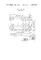
- FIG. 3 shows an embodiment of the semiconductor memory device according to the invention.
- This semiconductor memory circuit like the one shown in FIG. 1, comprises a matrix array of memory cells MC-11 to MC-MN, word lines W1 to WN each commonly connected to the memory cells in each row, data lines D0-1 to D0-M and D1-1 to D1-M each pair commonly connected to the memory cells in each column, a row decoder 2 for selecting one of the word lines W1 to WN in response to an address signal from an address signal generator circuit (not shown) and a column decoder 4 for selecting one pair of data lines D0-1 to D0-M and D1-1 to D1-M in response to an address signal from the address signal generator circuit.
- the memory cells MC-11 to MC-MN have a well-known construction, for instance, that of a cross-coupled memory cell as shown in FIG. 4 or that of a resistive load type n-channel MOS memory cell as shown in FIG. 5.
- the memory circuit further comprises a precharging circuit 6, which is connected to the data lines D0-1 to D0-M and D1-1 to D1-M and functions to precharge the pairs of data lines to the same potential level every time the address designating operation is started or ended, an input/output unit 8, which is connected through a pair of input/output lines 9-1 and 9-2 to the column decoder 4 and functions to enable data transfer between the selected one of the memory cells MC-11 to MC-MN and an external circuit (not shown) and sense amplifiers SA-1 to SA-M connected to the respective pairs of the data lines.
- a precharging circuit 6 which is connected to the data lines D0-1 to D0-M and D1-1 to D1-M and functions to precharge the pairs of data lines to the same potential level every time the address designating operation is started or ended
- an input/output unit 8 which is connected through a pair of input/output lines 9-1 and 9-2 to the column decoder 4 and functions to enable data transfer between the selected one of the memory cells MC-11
- This semiconductor memory circuit in this embodiment is provided with a dummy decoder 20 for producing a dummy select signal for every address designating operation cycle, a dummy word line WD provided across the data lines D0-1 to D0-M and D1-1 to D1-M to transmit the dummy select signal from the dummy decoder 20, M number of dummy capacitors C1 to CM connected to the dummy word line WD and a clock pulse generator 22 for producing clock pulses for activating the sense amplifiers SA-1 to SA-M in response to the dummy selection signal supplied from the dummy decoder 20 through the dummy word line WD.
- the dummy word line WD is formed of, for instance, a polycrystalline silicon layer like the word lines W1 to WM.
- a control signal generating circuit 23 which produces a read enable signal and a control signal ⁇ .
- the read enable signal is set at a high level to effect the readout operation and set a low level for a preset period of time to effect the write-in operation as described later.
- the control signal ⁇ is set at a high level after a preset precharging period of time in each operation cycle.
- the dummy decoder 20 is adapted to energize the dummy word line WD at the same timing as that at which the row decoder 2 selectively energizes one of the word lines W1 to WM at the time of the address designating operation. It may have substantially the same construction as each decoder section of the row decoder 2, for instance as shown in FIG. 6. As shown in FIG. 3,
- a row decoder section 200 for energizing the word line W1 comprises a p-channel MOS transistor 200-1, which receives at its gate a control signal ⁇ supplied from the control signal generating circuit 23 and showing a high level after a precharge period during the readout period and has its source connected to a power supply terminal V D , p-channel MOS transistors 200-2 to 200-4, which each have their current paths connected in parallel with that of the MOS transistor 200-1 and their gates connected to respective address signal lines ADSl to ADS3, n-channel MOS transistors 200-5 to 200-8, which each have their current paths connected in series with that of the MOS transistor 200-4 between the power supply terminals V D and V S and their gates respectively connected to the gates of the MOS transistors 200-4, 200-3, 200-2 and 200-1, and a CMOS inverter 200-9 having an input terminal connected to the juncture between the MOS transistors 200-4 and 200-5 and an output terminal connected to the word line W1.
- a dummy decoder 201 comprises a MOS transistor 201-1, which receives the control signal ⁇ at its gate and has its source connected to the power supply terminal V D , p-channel MOS transistors 201-2 to 201-4, which each have their current paths connected in parallel with that of the MOS transistor 201-1, n-channel MOS transistors 201-5 to 201-8, which have their current paths connected in series with that of the MOS transistor 201-4 and their gates respectively connected to the gates of the MOS transistors 201-4, 201-3, 201-2 and 201-1, and a CMOS inverter 201-9 having an input terminal connected to the juncture between the MOS transistors 201-4 and 201-5 and an output terminal connected to the dummy word line WD.
- the dummy decoder 201 is practically the same as the row decoder section 200 except that in the former the gates of the MOS transistors 201-2 to 201-4 are not connected to the address signal lines.
- an inverter is coupled to at least one of the address signal lines ADSl to ADS3. Also, while in this example three address signal lines are used, it is possible to use a different number of address signal lines as well.
- the data lines D0 and D1 are both precharged to a predetermined potential level by the precharging circuit 6 (FIG. 3), while at the same time an address signal from the address signal generator circuit (not shown) is supplied to the address signal lines ADSl to ADS3.
- the address signal supplied is one for energizing the word line W1
- the MOS transistors 200-2 to 200-4 are rendered non-conductive while the MOS transistors 200-5 to 200-7 are rendered conductive at this time.
- the control signal ⁇ is subsequently produced from the control signal generating circuit 23, the MOS transistor 200-1 is rendered non-conductive while the MOS transistor 200-8 is rendered conductive.
- the input signal to the CMOS inverter 200-9 is inverted to a low level, so that a high level output signal is produced from the inverter 200-9 to energize the word line W1.
- the MOS transistors 201-2 to 201-4 are normally held non-conductive while the MOS transistors 201-5 to 201-7 are held conductive.
- the control signal ⁇ is received by the dummy decoder 201 in this state, the MOS transistor 201-1 is rendered non-conductive while the MOS transistor 201-8 is rendered conductive.
- the input signal to the CMOS inverter 201-9 is inverted to a low level, so that a high level output signal is produced from the inverter to energize the dummy word line WD.
- the row decoder section 200 and dummy decoder 201 are set in substantially the same state, so that the word lines W1 and WD are energized an equal period of time after the supply of the control signal ⁇ .
- FIG. 7 shows a different row decoder section 202 for selectively energizing the word line W1 and a dummy decoder 203 for energizing the dummy word line WD.
- the row decoder section 202 comprises a p-channel MOS transistor 202-1, which receives the control signal ⁇ at its gate and has its source connected to a power supply terminal V D , n-channel MOS transistors 202-2 to 202-5, which are connected in series with the MOS transistor 202-1 between power supply terminals V D and V S , with the MOS transistors 202-2 to 202-4 having their gates connected to respective address signal lines ADS4 to ADS6, and a CMOS inverter 202-6 having an input terminal connected to the juncture between the MOS transistors 202-1 and 202-2 and an output terminal connected to the word line WD.
- the dummy decoder 203 comprises a p-channel MOS transistor 203-1, which receives the control signal ⁇ at its gate and its source connected to the power supply terminal V D , n-channel MOS transistors 203-2 to 203-5, which are connected in series with the MOS transistor 203-1 between the power supply terminals V D and V S , with the MOS transistors 202-2 to 202-4 having their gates connected to the power supply terminal V D , and a CMOS inverter 203-6 having an input terminal connected to the junction between the MOS transistors 203-1 and 203-2 and an output terminal connected to the dummy word line WD.
- the dummy selection signal is supplied from the dummy decoder 20 to the dummy word line simultaneously with the supply of the row selection signal from the row decoder 20 to one of word lines W1 to WN.
- FIG. 8 shows a specific construction of the clock pulse generator 22. It comprises a CMOS inverter 220 including p- and n-channel MOS transistors 221 and 222, an n-channel MOS transistor 223 connected in series with the n-channel MOS transistor 222, p-channel MOS transistors 224 and 225 each having a source connected to a power supply terminal V D and a drain connected to an output terminal of the CMOS inverter 220, a CMOS inverter 226 having an input terminal connected to the drain of the MOS transistors 224 and 225, a CMOS inverter 227 having an input terminal connected to an output terminal of the CMOS inverter 226, and a CMOS inverter 228 having an input terminal connected to an output terminal of the CMOS inverter 227.
- CMOS inverter 220 including p- and n-channel MOS transistors 221 and 222, an n-channel MOS transistor 223 connected in series with the n
- the CMOS inverter 220 has its input terminal connected to a readout enable terminal RET, the MOS transistor 223 has its gate connected to a word line terminal WLT connected to the dummy word line WD, the MOS transistor 224 has its gate connected to the input terminal of the CMOS inverter 226, and the MOS transistor 225 has its gate connected to a control signal input terminal CST.
- the output terminal of the CMOS inverter 228 is connected to an input terminal of an inversion type delay circuit 230 formed of three CMOS inverters 231 to 233 which are serially connected and each include p- and n-channel MOS transistors.
- the output terminal of the delay circuit 230 is connected to one input terminal of an AND gate circuit 240 having the other input terminal connected to the output terminal of the CMOS inverter 228.
- the AND gate circuit 240 includes p-channel MOS transistors 241 to 243 whose sources are connected to the power supply terminal V D , n-channel MOS transistors 244 and 245 whose current paths are serially connected between the drain of the MOS transistor 242 and the power supply terminal V S , and an n-channel MOS transistor 246 whose current path is connected between the drain of the MOS transistor 243 and the power supply terminal V S .
- the gates of the MOS transistors 241 and 245 are connected to the output terminal of the delay circuit 230, the gates of the MOS transistors 242 and 244 are connected to the output terminal of the CMOS inverter 228, and the gates of the MOS transistors 243 and 246 are connected to the drain of the MOS transistor 241 and to a junction between the MOS transistors 242 and 244.
- a junction between the MOS transistors 243 and 246 is connected to a clock output terminal CKT which is connected to the sense amplifiers SA-1 to SA-M.
- the MOS transistors 221 and 222 are respectively rendered non-conductive and conductive in response to a read enable signal having a high level and applied to the read enable terminal RET.
- the data lines D0 and D1 are precharged to a preset potential level as shown in FIGS. 9B and 9C, for example.
- the MOS transistor 225 is rendered non-conductive by the control signal ⁇ shown in FIG. 9D.
- CMOS inverter 226 produces a high level output signal to render the MOS transistor 224 nonconductive.
- the high level signal from the CMOS inverter 226 is supplied after inversion through the CMOS inverter 227 to the CMOS inverter 228, so that the CMOS inverter 228 produces a high level output signal.
- the high level output signal from the CMOS inverter 228 is directly supplied to one input terminal of the AND gate circuit 240 and at the same time to the other input terminal of the AND gate circuit 240 through the inversion type delay circuit 230.
- the clock pulse generator 22 produces an output signal having a high level during the time corresponding to the delay time of the inversion type delay circuit 230.
- the high level output signal from the clock pulse generator 22 is supplied to the sense amplifiers SA-1 to SA-M to activate the sense amplifiers.
- a high level read enable signal is applied to the read enable terminal RET, and therefore the same operation as described with reference to FIGS. 9A to 9E is effected.
- the read enable signal is made low as shown in FIG. 10B to set up a write-in mode.
- the potentials on the data lines D0 and D1 are set at levels corresponding to new data to be written. In this example, the potential on the data line D0 is changed over from a low level to a high level as shown in FIG.
- the clock pulse generator 22 produces, as shown in FIG. 10F, an output signal having a high level during the time corresponding to the delay time of the inversion type delay circuit 230. That is, the clock pulse generator 22 produces a high level output signal in response to the trailing edge of the write-in mode setting signal.
- the high level output signal from the clock pulse generator 22 is supplied to the sense amplifiers SA-1 to SA-M to activate the same.
- a corresponding one of the sense amplifiers SA-1 to SA-M amplifies the potentials on the corresponding data lines D0 and D1 so that the potentials on the data lines D0 and D1 are quickly rise and fall as shown in FIGS. 10C and 10D, respectively.
- FIG. 10E shows a dummy selection signal corresponding to that shown in FIG. 9D.
- FIG. 11 shows an example of the construction of the sense amplifiers SA-1 to SA-M used here. It comprises p-channel MOS transistors 300 and 301 each having a source connected to a power supply terminal V D , n-channel MOS transistors 302 and 303, which have their drains respectively connected to the drains of the MOS transistors 300 and 301 and their sources connected to each other, and n-channel MOS transistors 304 and 305 connected in series between the source of the MOS transistors 302 and 303 and a power supply terminal V S .
- the MOS transistors 300 and 302 have their gates connected to each other and also connected to the drains of the MOS transistors 301 and 303 and to the data line D0.
- the MOS transistors 301 and 303 have their gates connected to each other and also connected to the drains of the MOS transistors 300 and 302 and to the data line D1.
- the MOS transistor 304 has its gate connected to a column selection terminal CT which is connected to a column selection line connected to the column decoder 4 (which is omitted in FIG. 3 for clarifying the drawing), and the MOS transistor 305 has its gate connected to a clock pulse reception terminal PT for receiving the clock pulse output of the clock pulse generator 22.
- the word line W1 is energized by a row selection signal from the row decoder 2, thus causing data to be read out from the memory cell MC-M1 to the data lines D0-M and D1-M.
- a column selection signal from the column decoder 4 is impressed upon the gate of the MOS transistor 304 to render this MOS transistor conductive.
- the clock pulse generator 22 supplies a clock pulse to the gate of the MOS transistor 305 at an instant when the potential difference between the data lines D0-M and D1-M in the neighborhood of this sense amplifier reaches such as a level that can be sensed by the sense amplifier, thus rendering the MOS transistor 305 conductive.
- the MOS transistors 301 and 302 are rendered conductive while the MOS transistors 300 and 303 are rendered non-conductive.
- the potential on the data line D0-M is raised to a higher level because the supply voltage V D is superimposed through the MOS transistor 301 in conduction, while the potential on the data line D1-M is lowered toward the reference potential level through the MOS transistors 302, 304 and 305 in conduction. In this way, the potential difference between the data lines D0-M and D1-M is quickly expanded.
- the dummy capacitors C1 to CM are connected to the dummy word line WD.
- These dummy capacitors C1 to CM may, for instance, be CMOS capacitors.
- the time elapsed until one of the memory cells MC-M1 to MC-MN is energized by the row selection signal from the row decoder 20 is substantially equal to the time until the dummy selection signal from the dummy decoder 200 is impressed as energizing signal upon the clock pulse generator 22. It is to be noted that the time required from the reception of the energizing signal by the clock pulse generator 22 till the generation of a clock pulse therefrom is not longer than the time required until data read out from, for instance, the memory cell MC-MN is supplied as effective data to the sense amplifier SA-M.
- the dummy word line WD narrower than the word lines W1 to WN or omit one or more of the capacitors C1 to CM. Further, similar effects may be obtained by forming the dummy word line WD thicker and thus reducing the resistance R D .
- the dummy word line WD and word lines W1 to WN are arranged substantially under the same conditions, they are influenced by the changes of ambient conditions such as ambient temperature in the same way, that is, the time constant ⁇ D for the dummy word line WD and the time constant ⁇ p for each of the word lines W1 to WN change in a predetermined relation to each other so that the optimum timing of activation of the sense amplifiers SA-1 to SA-M can be maintained.
- FIG. 12 shows a second embodiment of the semiconductor memory circuit according to the invention.
- This semiconductor memory circuit differs from that of FIG. 1 only in that in this circuit a sense amplifier 400 having output lines connected to a pair of input/output lines 9-1 and 9-2 of the input/output unit 8 is used in lieu of the sense amplifiers SA-1 to SA-M.
- FIG. 13 shows an example of the sense amplifier 100 used in the semiconductor memory circuit shown in FIG. 10. It comprises p- and n-channel MOS transistors 401 and 402 with the current paths connected in parallel with each other, p- and n-channel MOS transistors 403 and 404 with the current paths connected in parallel with each other, p-channel MOS transistors 405 and 406 with the sources connected to a power supply terminal V D , n-channel MOS transistors 407 and 408 with the drains respectively connected to the drains of the MOS transistors 405 and 406, and an n-channel MOS transistor 409 having the drain connected to the sources of the MOS transistors 407 and 408 and the source connected to a power supply terminal V S .
- the MOS transistors 402 and 403 have their gates commonly connected to a column selection terminal CT which is connected to column selection lines of the column decoder 4 (which are not shown in FIG. 12 for clarifying the drawing), and the MOS transistors 401 and 404 have their gates commonly connected to a terminal ICT for receiving a selection signal, the terminals CT and ICT being connected to receive selection signals in an inverted relation to each other.
- the MOS transistors 405 and 407 have their gates commonly connected to the drains of the MOS transistors 406 and 408 and also connected through the MOS transistors 403 and 404 to an input/output terminal IOT1 which is connected to the input/output line 9-2.
- the MOS transistors 406 and 408 have their gates commonly connected to the drains of the MOS transistors 405 and 407 and also connected to an input/output terminal IOT2 which is connected to the input/output line 9-1.
- the MOS transistor 409 has its gate connected to a clock pulse reception terminal PT which is connected to the output terminal of the clock pulse generator 22.
- the word line W1 is energized by a row selection signal from the row decoder 2, thus causing data to be read out from the memory cell MC-M1 to the data lines D0-M and D1-M.
- a column selection signal from the column decoder 4 is impressed upon the gates of the MOS transistors 402 and 403, so that an inversion signal obtained from the column selection signal is impressed upon the gates of the MOS transistors 401 and 404.
- the MOS transistors 401 and 404 are rendered conductive, whereby the data read out from the memory cell MC-M1 is transferred through the MOS transistors 401 to 404. It is assumed that high and low level data signals are impressed upon the respective terminals IOT1 and IOT2. When the difference between both the data signal levels is increased to such a level that can be sensed by the sense amplifier 400, a pulse is produced from the clock pulse generator 22 and impressed upon the gate of the MOS transistor 409 to turn this MOS transistor conductive, thus rendering the MOS transistors 406 and 407 conductive.
- the potential at the terminal IOT1 is raised in level by means of the high level voltage supplied to the power supply terminal V D , while the potential at the terminal IOT2 is lowered in level by means of the low level voltage applied to the reference voltage terminal V S . In this way, the potential difference between the data lines D0-M and D1-M is quickly expanded.
- FIG. 14 shows a further embodiment of the invention applied to a dynamic random access memory (DRAM).
- This DRAM comprises a first matrix array of memory cells MCO-11 to MCO-MN, a second matrix array of memory cells MC1-11 to MC1-MN, word lines W0-1 to W0-N and data lines D2-1 to D2-M coupled to the dynamic memory cells MC0-11 to MC0-MN and word lines W1-1 to W1-N and data lines D3-1 to D3-M.
- the word lines W0-1 to W0-N are connected to a row decoder 500, which is connected to an address signal generator (not shown) and functions to selectively energize one of the word lines W0-1 to W0-N in response to an address signal from the address signal generator.
- the word lines W1-1 to W1-N are connected to a row decoder 502 for selectively energizing one of them in response to an address signal.
- the data lines D2-1 to D2-M and D3-1 to D3-M are connected to a column decoder/sense amplifier 504 for selecting one of the data lines D2-1 to D2-M and corresponding one of the data lines D3-1 to D3-M.
- This DRAM further comprises a dummy word line WD0 arranged in the same way as the word lines W0-1 to W0-N, dummy memory cells MCD-01 to MCD-0M commonly connected to the dummy word line WD0 and also connected to the respective data lines D2-1 to D2-M, a dummy word line WD1 arranged in the same way as the word lines W1-1 to W1-N, and dummy memory cells MCD-11 to MCD-1M commonly connected to the dummy word line WD1 and also connected to the respective data lines D2-1 and D3-M.
- the dummy word lines WD0 and WD1 are connected to respective dummy decoders 506 and 508.
- the dummy decoder 506 produces a dummy selection signal when one of the word lines W1-1 to W1-N is energized by the row decoder 502, for instance, in response to an address signal, and the dummy decoder 508 produces a dummy selection signal when one of the word lines W0-1 to W0-N is energized. In other words, at the time of the address designating operation either dummy word line WD0 or WD1 is energized.
- the DRAM further comprises a clock pulse generator 510 and a sense amplifier circuit 504.
- the clock pulse generator 510 is connected to the dummy decoders 506 and 508, and it supplies a clock pulse to the sense amplifier circuit 504 for activating this circuit in response to a dummy selection signal supplied to the same through the dummy word line WD0 or WD1.
- capacitors used for the memory cells MC0-11 to MC0-MN and MC1-11 to MC1-MN have double the capacitance of capacitors used for the dummy memory cells MCD-01 to MCD-0M and MCD-11 to MCD-1M.
- the operation of this DRAM will now be described in connection with the case of reading out data from, for instance, the memory cell MC0-M1.
- the word line W0-1 is energized by the row decoder 500 at the same timing as that at which the dummy word line WD1 is energized by the dummy decoder 508 as in the previous embodiments.
- the memory cells MC0-M1 and MCD-1M are substantially simultaneously rendered conductive.
- a data signal of 0 level or V L level is read out from the memory cell MC0-M1 and transferred through the data line D2-M to the sense amplifier 504.
- a dummy data signal having a level of 1/2 V L is transferred from the dummy memory cell MCD-1M to the sense amplifier 504.
- the sense amplifier 504 detects the difference voltage between the data signals from the memory cells MC0-M1 and MCD-1M, whereupon a corresponding data is transferred through an input/output unit 512 to an external circuit (not shown).
- the DRAM of FIG. 14 it is also possible to adjust the timing of activating the sense amplifier 504 with a clock pulse from the clock pulse generator 510 by forming the dummy word lines WD0 and WD1 such that they have a different thickness or width from that of the word lines W0-1 to W0-N. Also, with this DRAM, like the previous embodiments, the dummy word lines WD0 and WD1 are arranged substantially in the same way as the word lines W0-1 to W0-N and W1-1 to W1-N, so that it is possible to maintain the optimum timing of activation of the sense amplifier 504 irrespective of the changes of ambient conditions.
Abstract
Description
Claims (27)
Applications Claiming Priority (3)
| Application Number | Priority Date | Filing Date | Title |
|---|---|---|---|
| JP54-95527 | 1979-07-26 | ||
| JP54095527A JPS6032911B2 (en) | 1979-07-26 | 1979-07-26 | semiconductor storage device |
| EP80104251.6 | 1980-07-18 |
Related Parent Applications (1)
| Application Number | Title | Priority Date | Filing Date |
|---|---|---|---|
| US06171264 Continuation-In-Part | 1980-07-22 |
Publications (1)
| Publication Number | Publication Date |
|---|---|
| US4435793A true US4435793A (en) | 1984-03-06 |
Family
ID=14140021
Family Applications (1)
| Application Number | Title | Priority Date | Filing Date |
|---|---|---|---|
| US06/373,624 Expired - Lifetime US4435793A (en) | 1979-07-26 | 1982-04-30 | Semiconductor memory device with dummy word line/sense amplifier activation |
Country Status (3)
| Country | Link |
|---|---|
| US (1) | US4435793A (en) |
| EP (1) | EP0023329A3 (en) |
| JP (1) | JPS6032911B2 (en) |
Cited By (157)
| Publication number | Priority date | Publication date | Assignee | Title |
|---|---|---|---|---|
| US4680701A (en) * | 1984-04-11 | 1987-07-14 | Texas Instruments Incorporated | Asynchronous high speed processor having high speed memories with domino circuits contained therein |
| US4685087A (en) * | 1983-08-31 | 1987-08-04 | Texas Instruments Incorporated | SRAM with constant pulse width |
| EP0281889A2 (en) * | 1987-02-27 | 1988-09-14 | Nec Corporation | Memory circuit with improved data output control |
| EP0281868A2 (en) * | 1987-02-26 | 1988-09-14 | Nec Corporation | Semiconductor memory device with protection cells |
| US4800304A (en) * | 1986-02-04 | 1989-01-24 | Fujitsu Limited | Time delay circuit for a semiconductor device |
| US4831593A (en) * | 1986-07-18 | 1989-05-16 | Hitachi, Ltd. | Semiconductor memory |
| US4841462A (en) * | 1984-11-21 | 1989-06-20 | Etat Francais, Administration Des P.T.T. (Centre National D'etudes Des Telecommunications) | Random access memory and linear interpolation circuit comprising application thereof |
| EP0329141A1 (en) * | 1988-02-19 | 1989-08-23 | Nec Corporation | Sense circuit incorporated in semiconductor memory device |
| US5027323A (en) * | 1988-01-14 | 1991-06-25 | Hitachi, Ltd. | Write pulse signal generating circuit for a semiconductor memory device |
| US5122987A (en) * | 1988-03-04 | 1992-06-16 | Mitsubishi Denki Kabushiki Kaisha | Semiconductor memory device with individually addressable space cells capable of driving a data bus |
| US5245584A (en) * | 1990-12-20 | 1993-09-14 | Vlsi Technology, Inc. | Method and apparatus for compensating for bit line delays in semiconductor memories |
| US5511031A (en) * | 1994-08-31 | 1996-04-23 | International Business Machines Corporation | Semiconductor memory system having sense amplifier being activated late during clock cycle |
| US6044024A (en) * | 1998-01-14 | 2000-03-28 | International Business Machines Corporation | Interactive method for self-adjusted access on embedded DRAM memory macros |
| DE10034255A1 (en) * | 2000-07-14 | 2002-01-31 | Infineon Technologies Ag | Circuit arrangement for reading and writing information on a memory cell array |
| KR100365429B1 (en) * | 1999-06-30 | 2002-12-18 | 주식회사 하이닉스반도체 | Low static current semiconductor memory device |
| US6714472B2 (en) * | 1999-02-25 | 2004-03-30 | Micron Technology, Inc. | Dummy wordline for controlling the timing of the firing of sense amplifiers in a memory device in relation to the firing of wordlines in the memory device |
| US6903437B1 (en) * | 2004-01-07 | 2005-06-07 | Micron Technology, Inc. | Semiconductor devices, capacitor antifuses, dynamic random access memories, and cell plate bias connection methods |
| US20060119406A1 (en) * | 2004-11-15 | 2006-06-08 | Stephan Henzler | Flip-flop with additional state storage in the event of turn-off |
| US20060275969A1 (en) * | 2003-06-03 | 2006-12-07 | Renesas Technology Corp. | Method of manufacturing semiconductor integrated circuit device, and semiconductor integrated circuit device made by its method |
| US20150063052A1 (en) * | 2013-08-30 | 2015-03-05 | Micron Technology, Inc. | Independently addressable memory array address spaces |
| US9430191B2 (en) | 2013-11-08 | 2016-08-30 | Micron Technology, Inc. | Division operations for memory |
| US9437256B2 (en) | 2013-09-19 | 2016-09-06 | Micron Technology, Inc. | Data shifting |
| US9449675B2 (en) | 2013-10-31 | 2016-09-20 | Micron Technology, Inc. | Apparatuses and methods for identifying an extremum value stored in an array of memory cells |
| US9449674B2 (en) | 2014-06-05 | 2016-09-20 | Micron Technology, Inc. | Performing logical operations using sensing circuitry |
| US9455020B2 (en) | 2014-06-05 | 2016-09-27 | Micron Technology, Inc. | Apparatuses and methods for performing an exclusive or operation using sensing circuitry |
| US9466340B2 (en) | 2013-07-26 | 2016-10-11 | Micron Technology, Inc. | Apparatuses and methods for performing compare operations using sensing circuitry |
| US9472265B2 (en) | 2013-03-04 | 2016-10-18 | Micron Technology, Inc. | Apparatuses and methods for performing logical operations using sensing circuitry |
| US9496023B2 (en) | 2014-06-05 | 2016-11-15 | Micron Technology, Inc. | Comparison operations on logical representations of values in memory |
| US9583163B2 (en) | 2015-02-03 | 2017-02-28 | Micron Technology, Inc. | Loop structure for operations in memory |
| US9589602B2 (en) | 2014-09-03 | 2017-03-07 | Micron Technology, Inc. | Comparison operations in memory |
| US9589607B2 (en) | 2013-08-08 | 2017-03-07 | Micron Technology, Inc. | Apparatuses and methods for performing logical operations using sensing circuitry |
| US9659610B1 (en) | 2016-05-18 | 2017-05-23 | Micron Technology, Inc. | Apparatuses and methods for shifting data |
| US9659605B1 (en) | 2016-04-20 | 2017-05-23 | Micron Technology, Inc. | Apparatuses and methods for performing corner turn operations using sensing circuitry |
| US9697876B1 (en) | 2016-03-01 | 2017-07-04 | Micron Technology, Inc. | Vertical bit vector shift in memory |
| US9704540B2 (en) | 2014-06-05 | 2017-07-11 | Micron Technology, Inc. | Apparatuses and methods for parity determination using sensing circuitry |
| US9704541B2 (en) | 2015-06-12 | 2017-07-11 | Micron Technology, Inc. | Simulating access lines |
| US9711207B2 (en) | 2014-06-05 | 2017-07-18 | Micron Technology, Inc. | Performing logical operations using sensing circuitry |
| US9711206B2 (en) | 2014-06-05 | 2017-07-18 | Micron Technology, Inc. | Performing logical operations using sensing circuitry |
| US9740607B2 (en) | 2014-09-03 | 2017-08-22 | Micron Technology, Inc. | Swap operations in memory |
| US9741399B2 (en) | 2015-03-11 | 2017-08-22 | Micron Technology, Inc. | Data shift by elements of a vector in memory |
| US9747960B2 (en) | 2014-12-01 | 2017-08-29 | Micron Technology, Inc. | Apparatuses and methods for converting a mask to an index |
| US9747961B2 (en) | 2014-09-03 | 2017-08-29 | Micron Technology, Inc. | Division operations in memory |
| US9761300B1 (en) | 2016-11-22 | 2017-09-12 | Micron Technology, Inc. | Data shift apparatuses and methods |
| US9767864B1 (en) | 2016-07-21 | 2017-09-19 | Micron Technology, Inc. | Apparatuses and methods for storing a data value in a sensing circuitry element |
| US9779019B2 (en) | 2014-06-05 | 2017-10-03 | Micron Technology, Inc. | Data storage layout |
| US9779784B2 (en) | 2014-10-29 | 2017-10-03 | Micron Technology, Inc. | Apparatuses and methods for performing logical operations using sensing circuitry |
| US9786335B2 (en) | 2014-06-05 | 2017-10-10 | Micron Technology, Inc. | Apparatuses and methods for performing logical operations using sensing circuitry |
| US9805772B1 (en) | 2016-10-20 | 2017-10-31 | Micron Technology, Inc. | Apparatuses and methods to selectively perform logical operations |
| US9818459B2 (en) | 2016-04-19 | 2017-11-14 | Micron Technology, Inc. | Invert operations using sensing circuitry |
| US9830999B2 (en) | 2014-06-05 | 2017-11-28 | Micron Technology, Inc. | Comparison operations in memory |
| US9836218B2 (en) | 2014-10-03 | 2017-12-05 | Micron Technology, Inc. | Computing reduction and prefix sum operations in memory |
| US9847110B2 (en) | 2014-09-03 | 2017-12-19 | Micron Technology, Inc. | Apparatuses and methods for storing a data value in multiple columns of an array corresponding to digits of a vector |
| US9892767B2 (en) | 2016-02-12 | 2018-02-13 | Micron Technology, Inc. | Data gathering in memory |
| US9899070B2 (en) | 2016-02-19 | 2018-02-20 | Micron Technology, Inc. | Modified decode for corner turn |
| US9898253B2 (en) | 2015-03-11 | 2018-02-20 | Micron Technology, Inc. | Division operations on variable length elements in memory |
| US9898252B2 (en) | 2014-09-03 | 2018-02-20 | Micron Technology, Inc. | Multiplication operations in memory |
| US9904515B2 (en) | 2014-09-03 | 2018-02-27 | Micron Technology, Inc. | Multiplication operations in memory |
| US9905276B2 (en) | 2015-12-21 | 2018-02-27 | Micron Technology, Inc. | Control of sensing components in association with performing operations |
| US9910637B2 (en) | 2016-03-17 | 2018-03-06 | Micron Technology, Inc. | Signed division in memory |
| US9910787B2 (en) | 2014-06-05 | 2018-03-06 | Micron Technology, Inc. | Virtual address table |
| US9921777B2 (en) | 2015-06-22 | 2018-03-20 | Micron Technology, Inc. | Apparatuses and methods for data transfer from sensing circuitry to a controller |
| US9934856B2 (en) | 2014-03-31 | 2018-04-03 | Micron Technology, Inc. | Apparatuses and methods for comparing data patterns in memory |
| US9940026B2 (en) | 2014-10-03 | 2018-04-10 | Micron Technology, Inc. | Multidimensional contiguous memory allocation |
| US9952925B2 (en) | 2016-01-06 | 2018-04-24 | Micron Technology, Inc. | Error code calculation on sensing circuitry |
| US9959923B2 (en) | 2015-04-16 | 2018-05-01 | Micron Technology, Inc. | Apparatuses and methods to reverse data stored in memory |
| US9972367B2 (en) | 2016-07-21 | 2018-05-15 | Micron Technology, Inc. | Shifting data in sensing circuitry |
| US9971541B2 (en) | 2016-02-17 | 2018-05-15 | Micron Technology, Inc. | Apparatuses and methods for data movement |
| US9990181B2 (en) | 2016-08-03 | 2018-06-05 | Micron Technology, Inc. | Apparatuses and methods for random number generation |
| US9996479B2 (en) | 2015-08-17 | 2018-06-12 | Micron Technology, Inc. | Encryption of executables in computational memory |
| US9997212B1 (en) | 2017-04-24 | 2018-06-12 | Micron Technology, Inc. | Accessing data in memory |
| US9997232B2 (en) | 2016-03-10 | 2018-06-12 | Micron Technology, Inc. | Processing in memory (PIM) capable memory device having sensing circuitry performing logic operations |
| US10013197B1 (en) | 2017-06-01 | 2018-07-03 | Micron Technology, Inc. | Shift skip |
| US10014034B2 (en) | 2016-10-06 | 2018-07-03 | Micron Technology, Inc. | Shifting data in sensing circuitry |
| US10032493B2 (en) | 2015-01-07 | 2018-07-24 | Micron Technology, Inc. | Longest element length determination in memory |
| US10037785B2 (en) | 2016-07-08 | 2018-07-31 | Micron Technology, Inc. | Scan chain operation in sensing circuitry |
| US10043570B1 (en) | 2017-04-17 | 2018-08-07 | Micron Technology, Inc. | Signed element compare in memory |
| US10042608B2 (en) | 2016-05-11 | 2018-08-07 | Micron Technology, Inc. | Signed division in memory |
| US10049054B2 (en) | 2015-04-01 | 2018-08-14 | Micron Technology, Inc. | Virtual register file |
| US10049721B1 (en) | 2017-03-27 | 2018-08-14 | Micron Technology, Inc. | Apparatuses and methods for in-memory operations |
| US10049707B2 (en) | 2016-06-03 | 2018-08-14 | Micron Technology, Inc. | Shifting data |
| US10048888B2 (en) | 2016-02-10 | 2018-08-14 | Micron Technology, Inc. | Apparatuses and methods for partitioned parallel data movement |
| US20180239712A1 (en) * | 2017-02-21 | 2018-08-23 | Micron Technology, Inc. | Memory array page table walk |
| US10061590B2 (en) | 2015-01-07 | 2018-08-28 | Micron Technology, Inc. | Generating and executing a control flow |
| US10068652B2 (en) | 2014-09-03 | 2018-09-04 | Micron Technology, Inc. | Apparatuses and methods for determining population count |
| US10068664B1 (en) | 2017-05-19 | 2018-09-04 | Micron Technology, Inc. | Column repair in memory |
| US10074407B2 (en) | 2014-06-05 | 2018-09-11 | Micron Technology, Inc. | Apparatuses and methods for performing invert operations using sensing circuitry |
| US10074416B2 (en) | 2016-03-28 | 2018-09-11 | Micron Technology, Inc. | Apparatuses and methods for data movement |
| US10073786B2 (en) | 2015-05-28 | 2018-09-11 | Micron Technology, Inc. | Apparatuses and methods for compute enabled cache |
| US10073635B2 (en) | 2014-12-01 | 2018-09-11 | Micron Technology, Inc. | Multiple endianness compatibility |
| US10120740B2 (en) | 2016-03-22 | 2018-11-06 | Micron Technology, Inc. | Apparatus and methods for debugging on a memory device |
| US10140104B2 (en) | 2015-04-14 | 2018-11-27 | Micron Technology, Inc. | Target architecture determination |
| US10147467B2 (en) | 2017-04-17 | 2018-12-04 | Micron Technology, Inc. | Element value comparison in memory |
| US10147480B2 (en) | 2014-10-24 | 2018-12-04 | Micron Technology, Inc. | Sort operation in memory |
| US10146537B2 (en) | 2015-03-13 | 2018-12-04 | Micron Technology, Inc. | Vector population count determination in memory |
| US10153008B2 (en) | 2016-04-20 | 2018-12-11 | Micron Technology, Inc. | Apparatuses and methods for performing corner turn operations using sensing circuitry |
| US10152271B1 (en) | 2017-06-07 | 2018-12-11 | Micron Technology, Inc. | Data replication |
| US10162005B1 (en) | 2017-08-09 | 2018-12-25 | Micron Technology, Inc. | Scan chain operations |
| US10163467B2 (en) | 2014-10-16 | 2018-12-25 | Micron Technology, Inc. | Multiple endianness compatibility |
| US10185674B2 (en) | 2017-03-22 | 2019-01-22 | Micron Technology, Inc. | Apparatus and methods for in data path compute operations |
| US10199088B2 (en) | 2016-03-10 | 2019-02-05 | Micron Technology, Inc. | Apparatuses and methods for cache invalidate |
| US10236038B2 (en) | 2017-05-15 | 2019-03-19 | Micron Technology, Inc. | Bank to bank data transfer |
| US10262701B2 (en) | 2017-06-07 | 2019-04-16 | Micron Technology, Inc. | Data transfer between subarrays in memory |
| US10268389B2 (en) | 2017-02-22 | 2019-04-23 | Micron Technology, Inc. | Apparatuses and methods for in-memory operations |
| US10289542B2 (en) | 2015-02-06 | 2019-05-14 | Micron Technology, Inc. | Apparatuses and methods for memory device as a store for block program instructions |
| US10303632B2 (en) | 2016-07-26 | 2019-05-28 | Micron Technology, Inc. | Accessing status information |
| US10318168B2 (en) | 2017-06-19 | 2019-06-11 | Micron Technology, Inc. | Apparatuses and methods for simultaneous in data path compute operations |
| US10332586B1 (en) | 2017-12-19 | 2019-06-25 | Micron Technology, Inc. | Apparatuses and methods for subrow addressing |
| US10346092B2 (en) | 2017-08-31 | 2019-07-09 | Micron Technology, Inc. | Apparatuses and methods for in-memory operations using timing circuitry |
| US10365851B2 (en) | 2015-03-12 | 2019-07-30 | Micron Technology, Inc. | Apparatuses and methods for data movement |
| US10373666B2 (en) | 2016-11-08 | 2019-08-06 | Micron Technology, Inc. | Apparatuses and methods for compute components formed over an array of memory cells |
| US10379772B2 (en) | 2016-03-16 | 2019-08-13 | Micron Technology, Inc. | Apparatuses and methods for operations using compressed and decompressed data |
| US10388360B2 (en) | 2016-07-19 | 2019-08-20 | Micron Technology, Inc. | Utilization of data stored in an edge section of an array |
| US10387299B2 (en) | 2016-07-20 | 2019-08-20 | Micron Technology, Inc. | Apparatuses and methods for transferring data |
| US10387046B2 (en) | 2016-06-22 | 2019-08-20 | Micron Technology, Inc. | Bank to bank data transfer |
| US10388393B2 (en) | 2016-03-22 | 2019-08-20 | Micron Technology, Inc. | Apparatus and methods for debugging on a host and memory device |
| US10387058B2 (en) | 2016-09-29 | 2019-08-20 | Micron Technology, Inc. | Apparatuses and methods to change data category values |
| US10403352B2 (en) | 2017-02-22 | 2019-09-03 | Micron Technology, Inc. | Apparatuses and methods for compute in data path |
| US10409739B2 (en) | 2017-10-24 | 2019-09-10 | Micron Technology, Inc. | Command selection policy |
| US10416927B2 (en) | 2017-08-31 | 2019-09-17 | Micron Technology, Inc. | Processing in memory |
| US10423353B2 (en) | 2016-11-11 | 2019-09-24 | Micron Technology, Inc. | Apparatuses and methods for memory alignment |
| US10430244B2 (en) | 2016-03-28 | 2019-10-01 | Micron Technology, Inc. | Apparatuses and methods to determine timing of operations |
| US10440341B1 (en) | 2018-06-07 | 2019-10-08 | Micron Technology, Inc. | Image processor formed in an array of memory cells |
| US10437557B2 (en) | 2018-01-31 | 2019-10-08 | Micron Technology, Inc. | Determination of a match between data values stored by several arrays |
| US10453502B2 (en) | 2016-04-04 | 2019-10-22 | Micron Technology, Inc. | Memory bank power coordination including concurrently performing a memory operation in a selected number of memory regions |
| US10466928B2 (en) | 2016-09-15 | 2019-11-05 | Micron Technology, Inc. | Updating a register in memory |
| US10468087B2 (en) | 2016-07-28 | 2019-11-05 | Micron Technology, Inc. | Apparatuses and methods for operations in a self-refresh state |
| US10474581B2 (en) | 2016-03-25 | 2019-11-12 | Micron Technology, Inc. | Apparatuses and methods for cache operations |
| US10483978B1 (en) | 2018-10-16 | 2019-11-19 | Micron Technology, Inc. | Memory device processing |
| US10496286B2 (en) | 2015-02-06 | 2019-12-03 | Micron Technology, Inc. | Apparatuses and methods for parallel writing to multiple memory device structures |
| US10522212B2 (en) | 2015-03-10 | 2019-12-31 | Micron Technology, Inc. | Apparatuses and methods for shift decisions |
| US10522210B2 (en) | 2017-12-14 | 2019-12-31 | Micron Technology, Inc. | Apparatuses and methods for subarray addressing |
| US10522199B2 (en) | 2015-02-06 | 2019-12-31 | Micron Technology, Inc. | Apparatuses and methods for scatter and gather |
| US10529409B2 (en) | 2016-10-13 | 2020-01-07 | Micron Technology, Inc. | Apparatuses and methods to perform logical operations using sensing circuitry |
| US10534553B2 (en) | 2017-08-30 | 2020-01-14 | Micron Technology, Inc. | Memory array accessibility |
| US10607665B2 (en) | 2016-04-07 | 2020-03-31 | Micron Technology, Inc. | Span mask generation |
| US10606587B2 (en) | 2016-08-24 | 2020-03-31 | Micron Technology, Inc. | Apparatus and methods related to microcode instructions indicating instruction types |
| US10614875B2 (en) | 2018-01-30 | 2020-04-07 | Micron Technology, Inc. | Logical operations using memory cells |
| US10725696B2 (en) | 2018-04-12 | 2020-07-28 | Micron Technology, Inc. | Command selection policy with read priority |
| US10733089B2 (en) | 2016-07-20 | 2020-08-04 | Micron Technology, Inc. | Apparatuses and methods for write address tracking |
| US10741239B2 (en) | 2017-08-31 | 2020-08-11 | Micron Technology, Inc. | Processing in memory device including a row address strobe manager |
| US10838899B2 (en) | 2017-03-21 | 2020-11-17 | Micron Technology, Inc. | Apparatuses and methods for in-memory data switching networks |
| US10942843B2 (en) | 2017-04-25 | 2021-03-09 | Micron Technology, Inc. | Storing data elements of different lengths in respective adjacent rows or columns according to memory shapes |
| US10956439B2 (en) | 2016-02-19 | 2021-03-23 | Micron Technology, Inc. | Data transfer with a bit vector operation device |
| US10977033B2 (en) | 2016-03-25 | 2021-04-13 | Micron Technology, Inc. | Mask patterns generated in memory from seed vectors |
| US11029951B2 (en) | 2016-08-15 | 2021-06-08 | Micron Technology, Inc. | Smallest or largest value element determination |
| US11074988B2 (en) | 2016-03-22 | 2021-07-27 | Micron Technology, Inc. | Apparatus and methods for debugging on a host and memory device |
| US11175915B2 (en) | 2018-10-10 | 2021-11-16 | Micron Technology, Inc. | Vector registers implemented in memory |
| US11184446B2 (en) | 2018-12-05 | 2021-11-23 | Micron Technology, Inc. | Methods and apparatus for incentivizing participation in fog networks |
| US11194477B2 (en) | 2018-01-31 | 2021-12-07 | Micron Technology, Inc. | Determination of a match between data values stored by three or more arrays |
| US11222260B2 (en) | 2017-03-22 | 2022-01-11 | Micron Technology, Inc. | Apparatuses and methods for operating neural networks |
| US11227641B1 (en) | 2020-07-21 | 2022-01-18 | Micron Technology, Inc. | Arithmetic operations in memory |
| US11342031B2 (en) | 2020-08-28 | 2022-05-24 | Stmicroelectronics S.R.L. | Circuit and method for process and temperature compensated read voltage for non-volatile memory |
| US11360768B2 (en) | 2019-08-14 | 2022-06-14 | Micron Technolgy, Inc. | Bit string operations in memory |
| US11397688B2 (en) | 2018-10-10 | 2022-07-26 | Micron Technology, Inc. | Coherent memory access |
| US11398264B2 (en) | 2019-07-08 | 2022-07-26 | Micron Technology, Inc. | Methods and apparatus for dynamically adjusting performance of partitioned memory |
| US11449577B2 (en) | 2019-11-20 | 2022-09-20 | Micron Technology, Inc. | Methods and apparatus for performing video processing matrix operations within a memory array |
| US11853385B2 (en) | 2019-12-05 | 2023-12-26 | Micron Technology, Inc. | Methods and apparatus for performing diversity matrix operations within a memory array |
Families Citing this family (10)
| Publication number | Priority date | Publication date | Assignee | Title |
|---|---|---|---|---|
| DE3280064D1 (en) * | 1981-06-29 | 1990-01-18 | Fujitsu Ltd | DYNAMIC DIRECT ACCESS MEMORY ARRANGEMENT. |
| DE3307015A1 (en) * | 1983-02-28 | 1984-08-30 | Siemens AG, 1000 Berlin und 8000 München | READER AMPLIFIER CIRCUIT FOR A STATIC MOS MEMORY |
| US4627032A (en) * | 1983-11-25 | 1986-12-02 | At&T Bell Laboratories | Glitch lockout circuit for memory array |
| JPS6177198A (en) * | 1984-09-21 | 1986-04-19 | Toshiba Corp | Semiconductor memory |
| FR2592539B1 (en) * | 1985-12-31 | 1988-02-12 | Philips Ind Commerciale | PROGRAMMABLE NETWORK IN DYNAMIC LOGIC AND ITS APPLICATION. |
| JPS62222486A (en) * | 1986-02-14 | 1987-09-30 | Fujitsu Ltd | Connecting system for memory and peripheral circuit |
| JPH0194592A (en) * | 1987-10-06 | 1989-04-13 | Fujitsu Ltd | Semiconductor memory |
| JPH03160689A (en) * | 1989-11-17 | 1991-07-10 | Nec Corp | Semiconductor memory |
| IT1253678B (en) * | 1991-07-31 | 1995-08-22 | St Microelectronics Srl | ANTI-NOISE ARCHITECTURE FOR MEMORY |
| TW429683B (en) * | 1998-03-04 | 2001-04-11 | Siemens Ag | Improved dynamic access memory delay circuits and methods therefor |
Family Cites Families (2)
| Publication number | Priority date | Publication date | Assignee | Title |
|---|---|---|---|---|
| US4110842A (en) * | 1976-11-15 | 1978-08-29 | Advanced Micro Devices, Inc. | Random access memory with memory status for improved access and cycle times |
| US4162540A (en) * | 1978-03-20 | 1979-07-24 | Fujitsu Limited | Clocked memory with delay establisher by drive transistor design |
-
1979
- 1979-07-26 JP JP54095527A patent/JPS6032911B2/en not_active Expired
-
1980
- 1980-07-18 EP EP80104251A patent/EP0023329A3/en not_active Withdrawn
-
1982
- 1982-04-30 US US06/373,624 patent/US4435793A/en not_active Expired - Lifetime
Cited By (418)
| Publication number | Priority date | Publication date | Assignee | Title |
|---|---|---|---|---|
| US4685087A (en) * | 1983-08-31 | 1987-08-04 | Texas Instruments Incorporated | SRAM with constant pulse width |
| US4680701A (en) * | 1984-04-11 | 1987-07-14 | Texas Instruments Incorporated | Asynchronous high speed processor having high speed memories with domino circuits contained therein |
| US4841462A (en) * | 1984-11-21 | 1989-06-20 | Etat Francais, Administration Des P.T.T. (Centre National D'etudes Des Telecommunications) | Random access memory and linear interpolation circuit comprising application thereof |
| US4800304A (en) * | 1986-02-04 | 1989-01-24 | Fujitsu Limited | Time delay circuit for a semiconductor device |
| US4903235A (en) * | 1986-07-18 | 1990-02-20 | Hitachi, Ltd. | Semiconductor memory |
| US4831593A (en) * | 1986-07-18 | 1989-05-16 | Hitachi, Ltd. | Semiconductor memory |
| EP0281868A2 (en) * | 1987-02-26 | 1988-09-14 | Nec Corporation | Semiconductor memory device with protection cells |
| US4875194A (en) * | 1987-02-26 | 1989-10-17 | Nec Corporation | Semiconductor memory device with protection cells |
| EP0281868A3 (en) * | 1987-02-26 | 1990-09-26 | Nec Corporation | Semiconductor memory device with protection cells |
| EP0281889A2 (en) * | 1987-02-27 | 1988-09-14 | Nec Corporation | Memory circuit with improved data output control |
| EP0281889A3 (en) * | 1987-02-27 | 1990-07-18 | Nec Corporation | Memory circuit with improved data output control |
| US5027323A (en) * | 1988-01-14 | 1991-06-25 | Hitachi, Ltd. | Write pulse signal generating circuit for a semiconductor memory device |
| EP0329141A1 (en) * | 1988-02-19 | 1989-08-23 | Nec Corporation | Sense circuit incorporated in semiconductor memory device |
| US5122987A (en) * | 1988-03-04 | 1992-06-16 | Mitsubishi Denki Kabushiki Kaisha | Semiconductor memory device with individually addressable space cells capable of driving a data bus |
| US5245584A (en) * | 1990-12-20 | 1993-09-14 | Vlsi Technology, Inc. | Method and apparatus for compensating for bit line delays in semiconductor memories |
| US5511031A (en) * | 1994-08-31 | 1996-04-23 | International Business Machines Corporation | Semiconductor memory system having sense amplifier being activated late during clock cycle |
| US6044024A (en) * | 1998-01-14 | 2000-03-28 | International Business Machines Corporation | Interactive method for self-adjusted access on embedded DRAM memory macros |
| US6714472B2 (en) * | 1999-02-25 | 2004-03-30 | Micron Technology, Inc. | Dummy wordline for controlling the timing of the firing of sense amplifiers in a memory device in relation to the firing of wordlines in the memory device |
| KR100365429B1 (en) * | 1999-06-30 | 2002-12-18 | 주식회사 하이닉스반도체 | Low static current semiconductor memory device |
| DE10034255C2 (en) * | 2000-07-14 | 2002-05-16 | Infineon Technologies Ag | Circuit arrangement for reading and writing information on a memory cell array |
| US6487127B2 (en) | 2000-07-14 | 2002-11-26 | Infineon Technologies Ag | Circuit configuration for reading and writing information at a memory cell field |
| DE10034255A1 (en) * | 2000-07-14 | 2002-01-31 | Infineon Technologies Ag | Circuit arrangement for reading and writing information on a memory cell array |
| US20060275969A1 (en) * | 2003-06-03 | 2006-12-07 | Renesas Technology Corp. | Method of manufacturing semiconductor integrated circuit device, and semiconductor integrated circuit device made by its method |
| US6903437B1 (en) * | 2004-01-07 | 2005-06-07 | Micron Technology, Inc. | Semiconductor devices, capacitor antifuses, dynamic random access memories, and cell plate bias connection methods |
| US20050207256A1 (en) * | 2004-01-07 | 2005-09-22 | Manning H M | Semiconductor devices, capacitor antifuses, dynamic random access memories, and cell plate bias connection methods |
| US7683456B2 (en) | 2004-01-07 | 2010-03-23 | Micron Technology, Inc. | Semiconductor devices, capacitor antifuses, dynamic random access memories, and cell plate bias connection methods |
| US20060119406A1 (en) * | 2004-11-15 | 2006-06-08 | Stephan Henzler | Flip-flop with additional state storage in the event of turn-off |
| US7471580B2 (en) * | 2004-11-15 | 2008-12-30 | Infineon Technologies Ag | Flip-flop with additional state storage in the event of turn-off |
| US11727963B2 (en) | 2013-03-04 | 2023-08-15 | Micron Technology, Inc. | Apparatuses and methods for performing logical operations using sensing circuitry |
| US10796733B2 (en) | 2013-03-04 | 2020-10-06 | Micron Technology, Inc. | Apparatuses and methods for performing logical operations using sensing circuitry |
| US10153009B2 (en) | 2013-03-04 | 2018-12-11 | Micron Technology, Inc. | Apparatuses and methods for performing logical operations using sensing circuitry |
| US9892766B2 (en) | 2013-03-04 | 2018-02-13 | Micron Technology, Inc. | Apparatuses and methods for performing logical operations using sensing circuitry |
| US11276439B2 (en) | 2013-03-04 | 2022-03-15 | Micron Technology, Inc. | Apparatuses and methods for performing logical operations using sensing circuitry |
| US9959913B2 (en) | 2013-03-04 | 2018-05-01 | Micron Technology, Inc. | Apparatuses and methods for performing logical operations using sensing circuitry |
| US10431264B2 (en) | 2013-03-04 | 2019-10-01 | Micron Technology, Inc. | Apparatuses and methods for performing logical operations using sensing circuitry |
| US9472265B2 (en) | 2013-03-04 | 2016-10-18 | Micron Technology, Inc. | Apparatuses and methods for performing logical operations using sensing circuitry |
| US10056122B2 (en) | 2013-07-26 | 2018-08-21 | Micron Technology, Inc. | Apparatuses and methods for performing compare operations using sensing circuitry |
| US10643673B2 (en) | 2013-07-26 | 2020-05-05 | Micron Technology, Inc. | Apparatuses and methods for performing compare operations using sensing circuitry |
| US9466340B2 (en) | 2013-07-26 | 2016-10-11 | Micron Technology, Inc. | Apparatuses and methods for performing compare operations using sensing circuitry |
| US9799378B2 (en) | 2013-07-26 | 2017-10-24 | Micron Technology, Inc. | Apparatuses and methods for performing compare operations using sensing circuitry |
| US10535384B2 (en) | 2013-08-08 | 2020-01-14 | Micron Technology, Inc. | Apparatuses and methods for performing logical operations using sensing circuitry |
| US9899068B2 (en) | 2013-08-08 | 2018-02-20 | Micron Technology, Inc. | Apparatuses and methods for performing logical operations using sensing circuitry |
| US10878863B2 (en) | 2013-08-08 | 2020-12-29 | Micron Technology, Inc. | Apparatuses and methods for performing logical operations using sensing circuitry |
| US10186303B2 (en) | 2013-08-08 | 2019-01-22 | Micron Technology, Inc. | Apparatuses and methods for performing logical operations using sensing circuitry |
| US9589607B2 (en) | 2013-08-08 | 2017-03-07 | Micron Technology, Inc. | Apparatuses and methods for performing logical operations using sensing circuitry |
| US11495274B2 (en) | 2013-08-08 | 2022-11-08 | Micron Technology, Inc. | Apparatuses and methods for performing logical operations using sensing circuitry |
| US20150063052A1 (en) * | 2013-08-30 | 2015-03-05 | Micron Technology, Inc. | Independently addressable memory array address spaces |
| US9530475B2 (en) | 2013-08-30 | 2016-12-27 | Micron Technology, Inc. | Independently addressable memory array address spaces |
| CN105612582A (en) * | 2013-08-30 | 2016-05-25 | 美光科技公司 | Independently addressable memory array address spaces |
| US9153305B2 (en) * | 2013-08-30 | 2015-10-06 | Micron Technology, Inc. | Independently addressable memory array address spaces |
| KR101681460B1 (en) | 2013-08-30 | 2016-11-30 | 마이크론 테크놀로지, 인크 | Independently addressable memory array address spaces |
| US10043556B2 (en) | 2013-09-19 | 2018-08-07 | Micron Technology, Inc. | Data shifting |
| US9830955B2 (en) | 2013-09-19 | 2017-11-28 | Micron Technology, Inc. | Data shifting |
| US9437256B2 (en) | 2013-09-19 | 2016-09-06 | Micron Technology, Inc. | Data shifting |
| US9449675B2 (en) | 2013-10-31 | 2016-09-20 | Micron Technology, Inc. | Apparatuses and methods for identifying an extremum value stored in an array of memory cells |
| US9430191B2 (en) | 2013-11-08 | 2016-08-30 | Micron Technology, Inc. | Division operations for memory |
| US10579336B2 (en) | 2013-11-08 | 2020-03-03 | Micron Technology, Inc. | Division operations for memory |
| US10055196B2 (en) | 2013-11-08 | 2018-08-21 | Micron Technology, Inc. | Division operations for memory |
| US11393531B2 (en) | 2014-03-31 | 2022-07-19 | Micron Technology, Inc. | Apparatuses and methods for comparing data patterns in memory |
| US9934856B2 (en) | 2014-03-31 | 2018-04-03 | Micron Technology, Inc. | Apparatuses and methods for comparing data patterns in memory |
| US10726919B2 (en) | 2014-03-31 | 2020-07-28 | Micron Technology, Inc. | Apparatuses and methods for comparing data patterns in memory |
| US9830999B2 (en) | 2014-06-05 | 2017-11-28 | Micron Technology, Inc. | Comparison operations in memory |
| US10381065B2 (en) | 2014-06-05 | 2019-08-13 | Micron Technology, Inc. | Performing logical operations using sensing circuitry |
| US11238920B2 (en) | 2014-06-05 | 2022-02-01 | Micron Technology, Inc. | Comparison operations in memory |
| US11205497B2 (en) | 2014-06-05 | 2021-12-21 | Micron Technology, Inc. | Comparison operations in memory |
| US9449674B2 (en) | 2014-06-05 | 2016-09-20 | Micron Technology, Inc. | Performing logical operations using sensing circuitry |
| US10210911B2 (en) | 2014-06-05 | 2019-02-19 | Micron Technology, Inc. | Apparatuses and methods for performing logical operations using sensing circuitry in a memory device |
| US10249350B2 (en) | 2014-06-05 | 2019-04-02 | Micron Technology, Inc. | Apparatuses and methods for parity determination using sensing circuitry |
| US10255193B2 (en) | 2014-06-05 | 2019-04-09 | Micron Technology, Inc. | Virtual address table |
| US9779019B2 (en) | 2014-06-05 | 2017-10-03 | Micron Technology, Inc. | Data storage layout |
| US11120850B2 (en) | 2014-06-05 | 2021-09-14 | Micron Technology, Inc. | Performing logical operations using sensing circuitry |
| US10090041B2 (en) | 2014-06-05 | 2018-10-02 | Micro Technology, Inc. | Performing logical operations using sensing circuitry |
| US10290344B2 (en) | 2014-06-05 | 2019-05-14 | Micron Technology, Inc. | Performing logical operations using sensing circuitry |
| US10304519B2 (en) | 2014-06-05 | 2019-05-28 | Micron Technology, Inc. | Apparatuses and methods for performing an exclusive or operation using sensing circuitry |
| US10074407B2 (en) | 2014-06-05 | 2018-09-11 | Micron Technology, Inc. | Apparatuses and methods for performing invert operations using sensing circuitry |
| US10360147B2 (en) | 2014-06-05 | 2019-07-23 | Micron Technology, Inc. | Data storage layout |
| US9786335B2 (en) | 2014-06-05 | 2017-10-10 | Micron Technology, Inc. | Apparatuses and methods for performing logical operations using sensing circuitry |
| US9455020B2 (en) | 2014-06-05 | 2016-09-27 | Micron Technology, Inc. | Apparatuses and methods for performing an exclusive or operation using sensing circuitry |
| US9496023B2 (en) | 2014-06-05 | 2016-11-15 | Micron Technology, Inc. | Comparison operations on logical representations of values in memory |
| US9910787B2 (en) | 2014-06-05 | 2018-03-06 | Micron Technology, Inc. | Virtual address table |
| US10839892B2 (en) | 2014-06-05 | 2020-11-17 | Micron Technology, Inc. | Comparison operations in memory |
| US10839867B2 (en) | 2014-06-05 | 2020-11-17 | Micron Technology, Inc. | Apparatuses and methods for parity determination using sensing circuitry |
| US10424350B2 (en) | 2014-06-05 | 2019-09-24 | Micron Technology, Inc. | Performing logical operations using sensing circuitry |
| US11355178B2 (en) | 2014-06-05 | 2022-06-07 | Micron Technology, Inc. | Apparatuses and methods for performing an exclusive or operation using sensing circuitry |
| US10453499B2 (en) | 2014-06-05 | 2019-10-22 | Micron Technology, Inc. | Apparatuses and methods for performing an in-place inversion using sensing circuitry |
| US10490257B2 (en) | 2014-06-05 | 2019-11-26 | Micron Technology, Inc. | Comparison operations in memory |
| US11422933B2 (en) | 2014-06-05 | 2022-08-23 | Micron Technology, Inc. | Data storage layout |
| US10754787B2 (en) | 2014-06-05 | 2020-08-25 | Micron Technology, Inc. | Virtual address table |
| US10734038B2 (en) | 2014-06-05 | 2020-08-04 | Micron Technology, Inc. | Apparatuses and methods for performing logical operations using sensing circuitry |
| US9741427B2 (en) | 2014-06-05 | 2017-08-22 | Micron Technology, Inc. | Performing logical operations using sensing circuitry |
| US10522211B2 (en) | 2014-06-05 | 2019-12-31 | Micron Technology, Inc. | Performing logical operations using sensing circuitry |
| US9704540B2 (en) | 2014-06-05 | 2017-07-11 | Micron Technology, Inc. | Apparatuses and methods for parity determination using sensing circuitry |
| US9711207B2 (en) | 2014-06-05 | 2017-07-18 | Micron Technology, Inc. | Performing logical operations using sensing circuitry |
| US10593418B2 (en) | 2014-06-05 | 2020-03-17 | Micron Technology, Inc. | Comparison operations in memory |
| US9711206B2 (en) | 2014-06-05 | 2017-07-18 | Micron Technology, Inc. | Performing logical operations using sensing circuitry |
| US10409555B2 (en) | 2014-09-03 | 2019-09-10 | Micron Technology, Inc. | Multiplication operations in memory |
| US9904515B2 (en) | 2014-09-03 | 2018-02-27 | Micron Technology, Inc. | Multiplication operations in memory |
| US10705798B2 (en) | 2014-09-03 | 2020-07-07 | Micron Technology, Inc. | Multiplication operations in memory |
| US10559360B2 (en) | 2014-09-03 | 2020-02-11 | Micron Technology, Inc. | Apparatuses and methods for determining population count |
| US10157126B2 (en) | 2014-09-03 | 2018-12-18 | Micron Technology, Inc. | Swap operations in memory |
| US10713011B2 (en) | 2014-09-03 | 2020-07-14 | Micron Technology, Inc. | Multiplication operations in memory |
| US9779789B2 (en) | 2014-09-03 | 2017-10-03 | Micron Technology, Inc. | Comparison operations in memory |
| US9740607B2 (en) | 2014-09-03 | 2017-08-22 | Micron Technology, Inc. | Swap operations in memory |
| US10032491B2 (en) | 2014-09-03 | 2018-07-24 | Micron Technology, Inc. | Apparatuses and methods for storing a data value in multiple columns |
| US9940981B2 (en) | 2014-09-03 | 2018-04-10 | Micron Technology, Inc. | Division operations in memory |
| US9940985B2 (en) | 2014-09-03 | 2018-04-10 | Micron Technology, Inc. | Comparison operations in memory |
| US10861563B2 (en) | 2014-09-03 | 2020-12-08 | Micron Technology, Inc. | Apparatuses and methods for determining population count |
| US9589602B2 (en) | 2014-09-03 | 2017-03-07 | Micron Technology, Inc. | Comparison operations in memory |
| US9747961B2 (en) | 2014-09-03 | 2017-08-29 | Micron Technology, Inc. | Division operations in memory |
| US9847110B2 (en) | 2014-09-03 | 2017-12-19 | Micron Technology, Inc. | Apparatuses and methods for storing a data value in multiple columns of an array corresponding to digits of a vector |
| US9898252B2 (en) | 2014-09-03 | 2018-02-20 | Micron Technology, Inc. | Multiplication operations in memory |
| US10068652B2 (en) | 2014-09-03 | 2018-09-04 | Micron Technology, Inc. | Apparatuses and methods for determining population count |
| US10409554B2 (en) | 2014-09-03 | 2019-09-10 | Micron Technology, Inc. | Multiplication operations in memory |
| US9836218B2 (en) | 2014-10-03 | 2017-12-05 | Micron Technology, Inc. | Computing reduction and prefix sum operations in memory |
| US10540093B2 (en) | 2014-10-03 | 2020-01-21 | Micron Technology, Inc. | Multidimensional contiguous memory allocation |
| US10956043B2 (en) | 2014-10-03 | 2021-03-23 | Micron Technology, Inc. | Computing reduction and prefix sum operations in memory |
| US11768600B2 (en) | 2014-10-03 | 2023-09-26 | Micron Technology, Inc. | Computing reduction and prefix sum operations in memory |
| US9940026B2 (en) | 2014-10-03 | 2018-04-10 | Micron Technology, Inc. | Multidimensional contiguous memory allocation |
| US10261691B2 (en) | 2014-10-03 | 2019-04-16 | Micron Technology, Inc. | Computing reduction and prefix sum operations in memory |
| US10984842B2 (en) | 2014-10-16 | 2021-04-20 | Micron Technology, Inc. | Multiple endianness compatibility |
| US10163467B2 (en) | 2014-10-16 | 2018-12-25 | Micron Technology, Inc. | Multiple endianness compatibility |
| US10593377B2 (en) | 2014-10-16 | 2020-03-17 | Micron Technology, Inc. | Multiple endianness compatibility |
| US10685699B2 (en) | 2014-10-24 | 2020-06-16 | Micron Technology, Inc. | Sort operation in memory |
| US10147480B2 (en) | 2014-10-24 | 2018-12-04 | Micron Technology, Inc. | Sort operation in memory |
| US11315626B2 (en) | 2014-10-24 | 2022-04-26 | Micron Technology, Inc. | Sort operation in memory |
| US10074406B2 (en) | 2014-10-29 | 2018-09-11 | Micron Technology, Inc. | Apparatuses and methods for performing logical operations using sensing circuitry |
| US9779784B2 (en) | 2014-10-29 | 2017-10-03 | Micron Technology, Inc. | Apparatuses and methods for performing logical operations using sensing circuitry |
| US10529387B2 (en) | 2014-10-29 | 2020-01-07 | Micron Technology, Inc. | Apparatuses and methods for performing logical operations using sensing circuitry |
| US10073635B2 (en) | 2014-12-01 | 2018-09-11 | Micron Technology, Inc. | Multiple endianness compatibility |
| US10983706B2 (en) | 2014-12-01 | 2021-04-20 | Micron Technology, Inc. | Multiple endianness compatibility |
| US10037786B2 (en) | 2014-12-01 | 2018-07-31 | Micron Technology, Inc. | Apparatuses and methods for converting a mask to an index |
| US9747960B2 (en) | 2014-12-01 | 2017-08-29 | Micron Technology, Inc. | Apparatuses and methods for converting a mask to an index |
| US10387055B2 (en) | 2014-12-01 | 2019-08-20 | Micron Technology, Inc. | Multiple endianness compatibility |
| US10460773B2 (en) | 2014-12-01 | 2019-10-29 | Micron Technology, Inc. | Apparatuses and methods for converting a mask to an index |
| US10032493B2 (en) | 2015-01-07 | 2018-07-24 | Micron Technology, Inc. | Longest element length determination in memory |
| US10061590B2 (en) | 2015-01-07 | 2018-08-28 | Micron Technology, Inc. | Generating and executing a control flow |
| US11726791B2 (en) | 2015-01-07 | 2023-08-15 | Micron Technology, Inc. | Generating and executing a control flow |
| US10593376B2 (en) | 2015-01-07 | 2020-03-17 | Micron Technology, Inc. | Longest element length determination in memory |
| US10984841B2 (en) | 2015-01-07 | 2021-04-20 | Micron Technology, Inc. | Longest element length determination in memory |
| US11334362B2 (en) | 2015-01-07 | 2022-05-17 | Micron Technology, Inc. | Generating and executing a control flow |
| US10782980B2 (en) | 2015-01-07 | 2020-09-22 | Micron Technology, Inc. | Generating and executing a control flow |
| US9583163B2 (en) | 2015-02-03 | 2017-02-28 | Micron Technology, Inc. | Loop structure for operations in memory |
| US10176851B2 (en) | 2015-02-03 | 2019-01-08 | Micron Technology, Inc. | Loop structure for operations in memory |
| US11482260B2 (en) | 2015-02-06 | 2022-10-25 | Micron Technology, Inc. | Apparatuses and methods for scatter and gather |
| US11681440B2 (en) | 2015-02-06 | 2023-06-20 | Micron Technology, Inc. | Apparatuses and methods for parallel writing to multiple memory device structures |
| US11263123B2 (en) | 2015-02-06 | 2022-03-01 | Micron Technology, Inc. | Apparatuses and methods for memory device as a store for program instructions |
| US10522199B2 (en) | 2015-02-06 | 2019-12-31 | Micron Technology, Inc. | Apparatuses and methods for scatter and gather |
| US10289542B2 (en) | 2015-02-06 | 2019-05-14 | Micron Technology, Inc. | Apparatuses and methods for memory device as a store for block program instructions |
| US10942652B2 (en) | 2015-02-06 | 2021-03-09 | Micron Technology, Inc. | Apparatuses and methods for parallel writing to multiple memory device structures |
| US10496286B2 (en) | 2015-02-06 | 2019-12-03 | Micron Technology, Inc. | Apparatuses and methods for parallel writing to multiple memory device structures |
| US10817414B2 (en) | 2015-02-06 | 2020-10-27 | Micron Technology, Inc. | Apparatuses and methods for memory device as a store for block program instructions |
| US10964358B2 (en) | 2015-02-06 | 2021-03-30 | Micron Technology, Inc. | Apparatuses and methods for scatter and gather |
| US10522212B2 (en) | 2015-03-10 | 2019-12-31 | Micron Technology, Inc. | Apparatuses and methods for shift decisions |
| US11107520B2 (en) | 2015-03-10 | 2021-08-31 | Micron Technology, Inc. | Apparatuses and methods for shift decisions |
| US9928887B2 (en) | 2015-03-11 | 2018-03-27 | Micron Technology, Inc. | Data shift by elements of a vector in memory |
| US9898253B2 (en) | 2015-03-11 | 2018-02-20 | Micron Technology, Inc. | Division operations on variable length elements in memory |
| US9741399B2 (en) | 2015-03-11 | 2017-08-22 | Micron Technology, Inc. | Data shift by elements of a vector in memory |
| US10365851B2 (en) | 2015-03-12 | 2019-07-30 | Micron Technology, Inc. | Apparatuses and methods for data movement |
| US10936235B2 (en) | 2015-03-12 | 2021-03-02 | Micron Technology, Inc. | Apparatuses and methods for data movement |
| US11614877B2 (en) | 2015-03-12 | 2023-03-28 | Micron Technology, Inc. | Apparatuses and methods for data movement |
| US10896042B2 (en) | 2015-03-13 | 2021-01-19 | Micron Technology, Inc. | Vector population count determination via comparison iterations in memory |
| US10146537B2 (en) | 2015-03-13 | 2018-12-04 | Micron Technology, Inc. | Vector population count determination in memory |
| US11663005B2 (en) | 2015-03-13 | 2023-05-30 | Micron Technology, Inc. | Vector population count determination via comparsion iterations in memory |
| US10049054B2 (en) | 2015-04-01 | 2018-08-14 | Micron Technology, Inc. | Virtual register file |
| US10963398B2 (en) | 2015-04-01 | 2021-03-30 | Micron Technology, Inc. | Virtual register file |
| US11782688B2 (en) | 2015-04-14 | 2023-10-10 | Micron Technology, Inc. | Target architecture determination |
| US10140104B2 (en) | 2015-04-14 | 2018-11-27 | Micron Technology, Inc. | Target architecture determination |
| US11237808B2 (en) | 2015-04-14 | 2022-02-01 | Micron Technology, Inc. | Target architecture determination |
| US10795653B2 (en) | 2015-04-14 | 2020-10-06 | Micron Technology, Inc. | Target architecture determination |
| US10878884B2 (en) | 2015-04-16 | 2020-12-29 | Micron Technology, Inc. | Apparatuses and methods to reverse data stored in memory |
| US9959923B2 (en) | 2015-04-16 | 2018-05-01 | Micron Technology, Inc. | Apparatuses and methods to reverse data stored in memory |
| US10418092B2 (en) | 2015-04-16 | 2019-09-17 | Micron Technology, Inc. | Apparatuses and methods to reverse data stored in memory |
| US10073786B2 (en) | 2015-05-28 | 2018-09-11 | Micron Technology, Inc. | Apparatuses and methods for compute enabled cache |
| US10372612B2 (en) | 2015-05-28 | 2019-08-06 | Micron Technology, Inc. | Apparatuses and methods for compute enabled cache |
| US10970218B2 (en) | 2015-05-28 | 2021-04-06 | Micron Technology, Inc. | Apparatuses and methods for compute enabled cache |
| US11599475B2 (en) | 2015-05-28 | 2023-03-07 | Micron Technology, Inc. | Apparatuses and methods for compute enabled cache |
| US10431263B2 (en) | 2015-06-12 | 2019-10-01 | Micron Technology, Inc. | Simulating access lines |
| US9990966B2 (en) | 2015-06-12 | 2018-06-05 | Micron Technology, Inc. | Simulating access lines |
| US9704541B2 (en) | 2015-06-12 | 2017-07-11 | Micron Technology, Inc. | Simulating access lines |
| US10157019B2 (en) | 2015-06-22 | 2018-12-18 | Micron Technology, Inc. | Apparatuses and methods for data transfer from sensing circuitry to a controller |
| US9921777B2 (en) | 2015-06-22 | 2018-03-20 | Micron Technology, Inc. | Apparatuses and methods for data transfer from sensing circuitry to a controller |
| US11106389B2 (en) | 2015-06-22 | 2021-08-31 | Micron Technology, Inc. | Apparatuses and methods for data transfer from sensing circuitry to a controller |
| US9996479B2 (en) | 2015-08-17 | 2018-06-12 | Micron Technology, Inc. | Encryption of executables in computational memory |
| US11625336B2 (en) | 2015-08-17 | 2023-04-11 | Micron Technology, Inc. | Encryption of executables in computational memory |
| US10691620B2 (en) | 2015-08-17 | 2020-06-23 | Micron Technology, Inc. | Encryption of executables in computational memory |
| US9905276B2 (en) | 2015-12-21 | 2018-02-27 | Micron Technology, Inc. | Control of sensing components in association with performing operations |
| US10236037B2 (en) | 2015-12-21 | 2019-03-19 | Micron Technology, Inc. | Data transfer in sensing components |
| US11340983B2 (en) | 2016-01-06 | 2022-05-24 | Micron Technology, Inc. | Error code calculation on sensing circuitry |
| US10949299B2 (en) | 2016-01-06 | 2021-03-16 | Micron Technology, Inc. | Error code calculation on sensing circuitry |
| US10152374B2 (en) | 2016-01-06 | 2018-12-11 | Micron Technology, Inc. | Error code calculation on sensing circuitry |
| US10423486B2 (en) | 2016-01-06 | 2019-09-24 | Micron Technology, Inc. | Error code calculation on sensing circuitry |
| US11593200B2 (en) | 2016-01-06 | 2023-02-28 | Micron Technology, Inc. | Error code calculation on sensing circuitry |
| US9952925B2 (en) | 2016-01-06 | 2018-04-24 | Micron Technology, Inc. | Error code calculation on sensing circuitry |
| US10048888B2 (en) | 2016-02-10 | 2018-08-14 | Micron Technology, Inc. | Apparatuses and methods for partitioned parallel data movement |
| US11513713B2 (en) | 2016-02-10 | 2022-11-29 | Micron Technology, Inc. | Apparatuses and methods for partitioned parallel data movement |
| US10324654B2 (en) | 2016-02-10 | 2019-06-18 | Micron Technology, Inc. | Apparatuses and methods for partitioned parallel data movement |
| US10915263B2 (en) | 2016-02-10 | 2021-02-09 | Micron Technology, Inc. | Apparatuses and methods for partitioned parallel data movement |
| US9892767B2 (en) | 2016-02-12 | 2018-02-13 | Micron Technology, Inc. | Data gathering in memory |
| US10026459B2 (en) | 2016-02-12 | 2018-07-17 | Micron Technology, Inc. | Data gathering in memory |
| US10353618B2 (en) | 2016-02-17 | 2019-07-16 | Micron Technology, Inc. | Apparatuses and methods for data movement |
| US11010085B2 (en) | 2016-02-17 | 2021-05-18 | Micron Technology, Inc. | Apparatuses and methods for data movement |
| US11614878B2 (en) | 2016-02-17 | 2023-03-28 | Micron Technology, Inc. | Apparatuses and methods for data movement |
| US9971541B2 (en) | 2016-02-17 | 2018-05-15 | Micron Technology, Inc. | Apparatuses and methods for data movement |
| US10217499B2 (en) | 2016-02-19 | 2019-02-26 | Micron Technology, Inc. | Modified decode for corner turn |
| US10783942B2 (en) | 2016-02-19 | 2020-09-22 | Micron Technology, Inc. | Modified decode for corner turn |
| US11816123B2 (en) | 2016-02-19 | 2023-11-14 | Micron Technology, Inc. | Data transfer with a bit vector operation device |
| US10956439B2 (en) | 2016-02-19 | 2021-03-23 | Micron Technology, Inc. | Data transfer with a bit vector operation device |
| US9899070B2 (en) | 2016-02-19 | 2018-02-20 | Micron Technology, Inc. | Modified decode for corner turn |
| US9947376B2 (en) | 2016-03-01 | 2018-04-17 | Micron Technology, Inc. | Vertical bit vector shift in memory |
| US9697876B1 (en) | 2016-03-01 | 2017-07-04 | Micron Technology, Inc. | Vertical bit vector shift in memory |
| US10878883B2 (en) | 2016-03-10 | 2020-12-29 | Micron Technology, Inc. | Apparatuses and methods for cache invalidate |
| US10902906B2 (en) | 2016-03-10 | 2021-01-26 | Micron Technology, Inc. | Apparatuses and methods for logic/memory devices |
| US10262721B2 (en) | 2016-03-10 | 2019-04-16 | Micron Technology, Inc. | Apparatuses and methods for cache invalidate |
| US11594274B2 (en) | 2016-03-10 | 2023-02-28 | Micron Technology, Inc. | Processing in memory (PIM)capable memory device having timing circuity to control timing of operations |
| US9997232B2 (en) | 2016-03-10 | 2018-06-12 | Micron Technology, Inc. | Processing in memory (PIM) capable memory device having sensing circuitry performing logic operations |
| US11915741B2 (en) | 2016-03-10 | 2024-02-27 | Lodestar Licensing Group Llc | Apparatuses and methods for logic/memory devices |
| US10199088B2 (en) | 2016-03-10 | 2019-02-05 | Micron Technology, Inc. | Apparatuses and methods for cache invalidate |
| US10559347B2 (en) | 2016-03-10 | 2020-02-11 | Micron Technology, Inc. | Processing in memory (PIM) capable memory device having timing circuitry to control timing of operations |
| US11314429B2 (en) | 2016-03-16 | 2022-04-26 | Micron Technology, Inc. | Apparatuses and methods for operations using compressed and decompressed data |
| US10379772B2 (en) | 2016-03-16 | 2019-08-13 | Micron Technology, Inc. | Apparatuses and methods for operations using compressed and decompressed data |
| US10409557B2 (en) | 2016-03-17 | 2019-09-10 | Micron Technology, Inc. | Signed division in memory |
| US9910637B2 (en) | 2016-03-17 | 2018-03-06 | Micron Technology, Inc. | Signed division in memory |
| US10817360B2 (en) | 2016-03-22 | 2020-10-27 | Micron Technology, Inc. | Apparatus and methods for debugging on a memory device |
| US10388393B2 (en) | 2016-03-22 | 2019-08-20 | Micron Technology, Inc. | Apparatus and methods for debugging on a host and memory device |
| US11074988B2 (en) | 2016-03-22 | 2021-07-27 | Micron Technology, Inc. | Apparatus and methods for debugging on a host and memory device |
| US10120740B2 (en) | 2016-03-22 | 2018-11-06 | Micron Technology, Inc. | Apparatus and methods for debugging on a memory device |
| US10474581B2 (en) | 2016-03-25 | 2019-11-12 | Micron Technology, Inc. | Apparatuses and methods for cache operations |
| US11693783B2 (en) | 2016-03-25 | 2023-07-04 | Micron Technology, Inc. | Apparatuses and methods for cache operations |
| US10977033B2 (en) | 2016-03-25 | 2021-04-13 | Micron Technology, Inc. | Mask patterns generated in memory from seed vectors |
| US11775296B2 (en) | 2016-03-25 | 2023-10-03 | Micron Technology, Inc. | Mask patterns generated in memory from seed vectors |
| US11126557B2 (en) | 2016-03-25 | 2021-09-21 | Micron Technology, Inc. | Apparatuses and methods for cache operations |
| US10430244B2 (en) | 2016-03-28 | 2019-10-01 | Micron Technology, Inc. | Apparatuses and methods to determine timing of operations |
| US10698734B2 (en) | 2016-03-28 | 2020-06-30 | Micron Technology, Inc. | Apparatuses and methods to determine timing of operations |
| US11016811B2 (en) | 2016-03-28 | 2021-05-25 | Micron Technology, Inc. | Apparatuses and methods to determine timing of operations |
| US10482948B2 (en) | 2016-03-28 | 2019-11-19 | Micron Technology, Inc. | Apparatuses and methods for data movement |
| US10074416B2 (en) | 2016-03-28 | 2018-09-11 | Micron Technology, Inc. | Apparatuses and methods for data movement |
| US11557326B2 (en) | 2016-04-04 | 2023-01-17 | Micron Techology, Inc. | Memory power coordination |
| US11107510B2 (en) | 2016-04-04 | 2021-08-31 | Micron Technology, Inc. | Memory bank power coordination including concurrently performing a memory operation in a selected number of memory regions |
| US10453502B2 (en) | 2016-04-04 | 2019-10-22 | Micron Technology, Inc. | Memory bank power coordination including concurrently performing a memory operation in a selected number of memory regions |
| US10607665B2 (en) | 2016-04-07 | 2020-03-31 | Micron Technology, Inc. | Span mask generation |
| US11437079B2 (en) | 2016-04-07 | 2022-09-06 | Micron Technology, Inc. | Span mask generation |
| US10643674B2 (en) | 2016-04-19 | 2020-05-05 | Micron Technology, Inc. | Invert operations using sensing circuitry |
| US10134453B2 (en) | 2016-04-19 | 2018-11-20 | Micron Technology, Inc. | Invert operations using sensing circuitry |
| US9818459B2 (en) | 2016-04-19 | 2017-11-14 | Micron Technology, Inc. | Invert operations using sensing circuitry |
| US9990967B2 (en) | 2016-04-20 | 2018-06-05 | Micron Technology, Inc. | Apparatuses and methods for performing corner turn operations using sensing circuitry |
| US10699756B2 (en) | 2016-04-20 | 2020-06-30 | Micron Technology, Inc. | Apparatuses and methods for performing corner turn operations using sensing circuitry |
| US9659605B1 (en) | 2016-04-20 | 2017-05-23 | Micron Technology, Inc. | Apparatuses and methods for performing corner turn operations using sensing circuitry |
| US10153008B2 (en) | 2016-04-20 | 2018-12-11 | Micron Technology, Inc. | Apparatuses and methods for performing corner turn operations using sensing circuitry |
| US10540144B2 (en) | 2016-05-11 | 2020-01-21 | Micron Technology, Inc. | Signed division in memory |
| US10042608B2 (en) | 2016-05-11 | 2018-08-07 | Micron Technology, Inc. | Signed division in memory |
| US9659610B1 (en) | 2016-05-18 | 2017-05-23 | Micron Technology, Inc. | Apparatuses and methods for shifting data |
| US9899064B2 (en) | 2016-05-18 | 2018-02-20 | Micron Technology, Inc. | Apparatuses and methods for shifting data |
| US10311922B2 (en) | 2016-06-03 | 2019-06-04 | Micron Technology, Inc. | Shifting data |
| US10049707B2 (en) | 2016-06-03 | 2018-08-14 | Micron Technology, Inc. | Shifting data |
| US10658017B2 (en) | 2016-06-03 | 2020-05-19 | Micron Technology, Inc. | Shifting data |
| US11755206B2 (en) | 2016-06-22 | 2023-09-12 | Micron Technology, Inc. | Bank to bank data transfer |
| US10929023B2 (en) | 2016-06-22 | 2021-02-23 | Micron Technology, Inc. | Bank to bank data transfer |
| US10387046B2 (en) | 2016-06-22 | 2019-08-20 | Micron Technology, Inc. | Bank to bank data transfer |
| US10037785B2 (en) | 2016-07-08 | 2018-07-31 | Micron Technology, Inc. | Scan chain operation in sensing circuitry |
| US10388334B2 (en) | 2016-07-08 | 2019-08-20 | Micron Technology, Inc. | Scan chain operation in sensing circuitry |
| US10388360B2 (en) | 2016-07-19 | 2019-08-20 | Micron Technology, Inc. | Utilization of data stored in an edge section of an array |
| US10699772B2 (en) | 2016-07-19 | 2020-06-30 | Micron Technology, Inc. | Utilization of instructions stored in an edge section of an array of memory cells |
| US11468944B2 (en) | 2016-07-19 | 2022-10-11 | Micron Technology, Inc. | Utilization of data stored in an edge section of an array |
| US10929283B2 (en) | 2016-07-20 | 2021-02-23 | Micron Technology, Inc. | Apparatuses and methods for transferring data |
| US11513945B2 (en) | 2016-07-20 | 2022-11-29 | Micron Technology, Inc. | Apparatuses and methods for transferring data using a cache |
| US10387299B2 (en) | 2016-07-20 | 2019-08-20 | Micron Technology, Inc. | Apparatuses and methods for transferring data |
| US10733089B2 (en) | 2016-07-20 | 2020-08-04 | Micron Technology, Inc. | Apparatuses and methods for write address tracking |
| US9767864B1 (en) | 2016-07-21 | 2017-09-19 | Micron Technology, Inc. | Apparatuses and methods for storing a data value in a sensing circuitry element |
| US10839870B2 (en) | 2016-07-21 | 2020-11-17 | Micron Technology, Inc. | Apparatuses and methods for storing a data value in a sensing circuitry element |
| US10360949B2 (en) | 2016-07-21 | 2019-07-23 | Micron Technology, Inc. | Apparatuses and methods for storing a data value in a sensing circuitry element |
| US9966116B2 (en) | 2016-07-21 | 2018-05-08 | Micron Technology, Inc. | Apparatuses and methods for storing a data value in a sensing circuitry element |
| US10789996B2 (en) | 2016-07-21 | 2020-09-29 | Micron Technology, Inc. | Shifting data in sensing circuitry |
| US10242722B2 (en) | 2016-07-21 | 2019-03-26 | Micron Technology, Inc. | Shifting data in sensing circuitry |
| US9972367B2 (en) | 2016-07-21 | 2018-05-15 | Micron Technology, Inc. | Shifting data in sensing circuitry |
| US10725952B2 (en) | 2016-07-26 | 2020-07-28 | Micron Technology, Inc. | Accessing status information |
| US10303632B2 (en) | 2016-07-26 | 2019-05-28 | Micron Technology, Inc. | Accessing status information |
| US11282563B2 (en) | 2016-07-28 | 2022-03-22 | Micron Technology, Inc. | Apparatuses and methods for operations in a self-refresh state |
| US10468087B2 (en) | 2016-07-28 | 2019-11-05 | Micron Technology, Inc. | Apparatuses and methods for operations in a self-refresh state |
| US11664064B2 (en) | 2016-07-28 | 2023-05-30 | Micron Technology, Inc. | Apparatuses and methods for operations in a self-refresh state |
| US9990181B2 (en) | 2016-08-03 | 2018-06-05 | Micron Technology, Inc. | Apparatuses and methods for random number generation |
| US10152304B2 (en) | 2016-08-03 | 2018-12-11 | Micron Technology, Inc. | Apparatuses and methods for random number generation |
| US10387121B2 (en) | 2016-08-03 | 2019-08-20 | Micron Technology, Inc. | Apparatuses and methods for random number generation |
| US11029951B2 (en) | 2016-08-15 | 2021-06-08 | Micron Technology, Inc. | Smallest or largest value element determination |
| US11526355B2 (en) | 2016-08-15 | 2022-12-13 | Micron Technology, Inc. | Smallest or largest value element determination |
| US11061671B2 (en) | 2016-08-24 | 2021-07-13 | Micron Technology, Inc. | Apparatus and methods related to microcode instructions indicating instruction types |
| US10606587B2 (en) | 2016-08-24 | 2020-03-31 | Micron Technology, Inc. | Apparatus and methods related to microcode instructions indicating instruction types |
| US11842191B2 (en) | 2016-08-24 | 2023-12-12 | Micron Technology, Inc. | Apparatus and methods related to microcode instructions indicating instruction types |
| US11625194B2 (en) | 2016-09-15 | 2023-04-11 | Micron Technology, Inc. | Updating a register in memory |
| US10466928B2 (en) | 2016-09-15 | 2019-11-05 | Micron Technology, Inc. | Updating a register in memory |
| US11055026B2 (en) | 2016-09-15 | 2021-07-06 | Micron Technology, Inc. | Updating a register in memory |
| US10387058B2 (en) | 2016-09-29 | 2019-08-20 | Micron Technology, Inc. | Apparatuses and methods to change data category values |
| US10725680B2 (en) | 2016-09-29 | 2020-07-28 | Micron Technology, Inc. | Apparatuses and methods to change data category values |
| US11422720B2 (en) | 2016-09-29 | 2022-08-23 | Micron Technology, Inc. | Apparatuses and methods to change data category values |
| US10976943B2 (en) | 2016-09-29 | 2021-04-13 | Micron Technology, Inc. | Apparatuses and methods to change data category values |
| US10242721B2 (en) | 2016-10-06 | 2019-03-26 | Micron Technology, Inc. | Shifting data in sensing circuitry |
| US10014034B2 (en) | 2016-10-06 | 2018-07-03 | Micron Technology, Inc. | Shifting data in sensing circuitry |
| US10600473B2 (en) | 2016-10-13 | 2020-03-24 | Micron Technology, Inc. | Apparatuses and methods to perform logical operations using sensing circuitry |
| US10971214B2 (en) | 2016-10-13 | 2021-04-06 | Micron Technology, Inc. | Apparatuses and methods to perform logical operations using sensing circuitry |
| US10529409B2 (en) | 2016-10-13 | 2020-01-07 | Micron Technology, Inc. | Apparatuses and methods to perform logical operations using sensing circuitry |
| US10388333B2 (en) | 2016-10-20 | 2019-08-20 | Micron Technology, Inc. | Apparatuses and methods to selectively perform logical operations |
| US9805772B1 (en) | 2016-10-20 | 2017-10-31 | Micron Technology, Inc. | Apparatuses and methods to selectively perform logical operations |
| US10854247B2 (en) | 2016-10-20 | 2020-12-01 | Micron Technology, Inc. | Apparatuses and methods to selectively perform logical operations |
| US10373666B2 (en) | 2016-11-08 | 2019-08-06 | Micron Technology, Inc. | Apparatuses and methods for compute components formed over an array of memory cells |
| US10854269B2 (en) | 2016-11-08 | 2020-12-01 | Micron Technology, Inc. | Apparatuses and methods for compute components formed over an array of memory cells |
| US11238914B2 (en) | 2016-11-08 | 2022-02-01 | Micron Technology, Inc. | Apparatuses and methods for compute components formed over an array of memory cells |
| US10423353B2 (en) | 2016-11-11 | 2019-09-24 | Micron Technology, Inc. | Apparatuses and methods for memory alignment |
| US11048428B2 (en) | 2016-11-11 | 2021-06-29 | Micron Technology, Inc. | Apparatuses and methods for memory alignment |
| US11693576B2 (en) | 2016-11-11 | 2023-07-04 | Micron Technology, Inc. | Apparatuses and methods for memory alignment |
| US9761300B1 (en) | 2016-11-22 | 2017-09-12 | Micron Technology, Inc. | Data shift apparatuses and methods |
| US9940990B1 (en) | 2016-11-22 | 2018-04-10 | Micron Technology, Inc. | Data shift apparatuses and methods |
| US20180239712A1 (en) * | 2017-02-21 | 2018-08-23 | Micron Technology, Inc. | Memory array page table walk |
| US20220075733A1 (en) * | 2017-02-21 | 2022-03-10 | Micron Technology, Inc. | Memory array page table walk |
| US11182304B2 (en) | 2017-02-21 | 2021-11-23 | Micron Technology, Inc. | Memory array page table walk |
| CN110325972A (en) * | 2017-02-21 | 2019-10-11 | 美光科技公司 | Memory array page tabular seeks choosing |
| US10402340B2 (en) * | 2017-02-21 | 2019-09-03 | Micron Technology, Inc. | Memory array page table walk |
| US11663137B2 (en) * | 2017-02-21 | 2023-05-30 | Micron Technology, Inc. | Memory array page table walk |
| TWI699651B (en) * | 2017-02-21 | 2020-07-21 | 美商美光科技公司 | Memory apparatus and methods for operating the same |
| CN111949571A (en) * | 2017-02-21 | 2020-11-17 | 美光科技公司 | Memory array page table look-for-select |
| CN110325972B (en) * | 2017-02-21 | 2020-09-15 | 美光科技公司 | Memory array page table look-for-select |
| US10915249B2 (en) | 2017-02-22 | 2021-02-09 | Micron Technology, Inc. | Apparatuses and methods for in-memory operations |
| US11682449B2 (en) | 2017-02-22 | 2023-06-20 | Micron Technology, Inc. | Apparatuses and methods for compute in data path |
| US10540097B2 (en) | 2017-02-22 | 2020-01-21 | Micron Technology, Inc. | Apparatuses and methods for in-memory operations |
| US11011220B2 (en) | 2017-02-22 | 2021-05-18 | Micron Technology, Inc. | Apparatuses and methods for compute in data path |
| US10403352B2 (en) | 2017-02-22 | 2019-09-03 | Micron Technology, Inc. | Apparatuses and methods for compute in data path |
| US10268389B2 (en) | 2017-02-22 | 2019-04-23 | Micron Technology, Inc. | Apparatuses and methods for in-memory operations |
| US11474965B2 (en) | 2017-03-21 | 2022-10-18 | Micron Technology, Inc. | Apparatuses and methods for in-memory data switching networks |
| US10838899B2 (en) | 2017-03-21 | 2020-11-17 | Micron Technology, Inc. | Apparatuses and methods for in-memory data switching networks |
| US10452578B2 (en) | 2017-03-22 | 2019-10-22 | Micron Technology, Inc. | Apparatus and methods for in data path compute operations |
| US11550742B2 (en) | 2017-03-22 | 2023-01-10 | Micron Technology, Inc. | Apparatus and methods for in data path compute operations |
| US11048652B2 (en) | 2017-03-22 | 2021-06-29 | Micron Technology, Inc. | Apparatus and methods for in data path compute operations |
| US10817442B2 (en) | 2017-03-22 | 2020-10-27 | Micron Technology, Inc. | Apparatus and methods for in data path compute operations |
| US11222260B2 (en) | 2017-03-22 | 2022-01-11 | Micron Technology, Inc. | Apparatuses and methods for operating neural networks |
| US10185674B2 (en) | 2017-03-22 | 2019-01-22 | Micron Technology, Inc. | Apparatus and methods for in data path compute operations |
| US11769053B2 (en) | 2017-03-22 | 2023-09-26 | Micron Technology, Inc. | Apparatuses and methods for operating neural networks |
| US11410717B2 (en) | 2017-03-27 | 2022-08-09 | Micron Technology, Inc. | Apparatuses and methods for in-memory operations |
| US10049721B1 (en) | 2017-03-27 | 2018-08-14 | Micron Technology, Inc. | Apparatuses and methods for in-memory operations |
| US10878885B2 (en) | 2017-03-27 | 2020-12-29 | Micron Technology, Inc. | Apparatuses and methods for in-memory operations |
| US10446221B2 (en) | 2017-03-27 | 2019-10-15 | Micron Technology, Inc. | Apparatuses and methods for in-memory operations |
| US10147467B2 (en) | 2017-04-17 | 2018-12-04 | Micron Technology, Inc. | Element value comparison in memory |
| US10622034B2 (en) | 2017-04-17 | 2020-04-14 | Micron Technology, Inc. | Element value comparison in memory |
| US10043570B1 (en) | 2017-04-17 | 2018-08-07 | Micron Technology, Inc. | Signed element compare in memory |
| US10304502B2 (en) | 2017-04-24 | 2019-05-28 | Micron Technology, Inc. | Accessing data in memory |
| US10147468B2 (en) | 2017-04-24 | 2018-12-04 | Micron Technology, Inc. | Accessing data in memory |
| US9997212B1 (en) | 2017-04-24 | 2018-06-12 | Micron Technology, Inc. | Accessing data in memory |
| US11494296B2 (en) | 2017-04-25 | 2022-11-08 | Micron Technology, Inc. | Memory shapes |
| US10942843B2 (en) | 2017-04-25 | 2021-03-09 | Micron Technology, Inc. | Storing data elements of different lengths in respective adjacent rows or columns according to memory shapes |
| US10236038B2 (en) | 2017-05-15 | 2019-03-19 | Micron Technology, Inc. | Bank to bank data transfer |
| US10796736B2 (en) | 2017-05-15 | 2020-10-06 | Micron Technology, Inc. | Bank to bank data transfer |
| US11514957B2 (en) | 2017-05-15 | 2022-11-29 | Micron Technology, Inc. | Bank to bank data transfer |
| US10418123B2 (en) | 2017-05-19 | 2019-09-17 | Micron Technology, Inc. | Column repair in memory |
| US10068664B1 (en) | 2017-05-19 | 2018-09-04 | Micron Technology, Inc. | Column repair in memory |
| US10496310B2 (en) | 2017-06-01 | 2019-12-03 | Micron Technology, Inc. | Shift skip |
| US10013197B1 (en) | 2017-06-01 | 2018-07-03 | Micron Technology, Inc. | Shift skip |
| US10776037B2 (en) | 2017-06-07 | 2020-09-15 | Micron Technology, Inc. | Data replication |
| US11526293B2 (en) | 2017-06-07 | 2022-12-13 | Micron Technology, Inc. | Data replication |
| US10152271B1 (en) | 2017-06-07 | 2018-12-11 | Micron Technology, Inc. | Data replication |
| US10510381B2 (en) | 2017-06-07 | 2019-12-17 | Micron Technology, Inc. | Data transfer between subarrays in memory |
| US10878856B2 (en) | 2017-06-07 | 2020-12-29 | Micron Technology, Inc. | Data transfer between subarrays in memory |
| US10262701B2 (en) | 2017-06-07 | 2019-04-16 | Micron Technology, Inc. | Data transfer between subarrays in memory |
| US10795582B2 (en) | 2017-06-19 | 2020-10-06 | Micron Technology, Inc. | Apparatuses and methods for simultaneous in data path compute operations |
| US11693561B2 (en) | 2017-06-19 | 2023-07-04 | Micron Technology, Inc. | Apparatuses and methods for simultaneous in data path compute operations |
| US10318168B2 (en) | 2017-06-19 | 2019-06-11 | Micron Technology, Inc. | Apparatuses and methods for simultaneous in data path compute operations |
| US11372550B2 (en) | 2017-06-19 | 2022-06-28 | Micron Technology, Inc. | Apparatuses and methods for simultaneous in data path compute operations |
| US10712389B2 (en) | 2017-08-09 | 2020-07-14 | Micron Technology, Inc. | Scan chain operations |
| US10162005B1 (en) | 2017-08-09 | 2018-12-25 | Micron Technology, Inc. | Scan chain operations |
| US11182085B2 (en) | 2017-08-30 | 2021-11-23 | Micron Technology, Inc. | Memory array accessibility |
| US10534553B2 (en) | 2017-08-30 | 2020-01-14 | Micron Technology, Inc. | Memory array accessibility |
| US11886715B2 (en) | 2017-08-30 | 2024-01-30 | Lodestar Licensing Group Llc | Memory array accessibility |
| US11586389B2 (en) | 2017-08-31 | 2023-02-21 | Micron Technology, Inc. | Processing in memory |
| US11894045B2 (en) | 2017-08-31 | 2024-02-06 | Lodestar Licensing Group, Llc | Processing in memory implementing VLIW controller |
| US11163495B2 (en) | 2017-08-31 | 2021-11-02 | Micron Technology, Inc. | Processing in memory |
| US11016706B2 (en) | 2017-08-31 | 2021-05-25 | Micron Technology, Inc. | Apparatuses for in-memory operations |
| US10628085B2 (en) | 2017-08-31 | 2020-04-21 | Micron Technology, Inc. | Processing in memory |
| US10741239B2 (en) | 2017-08-31 | 2020-08-11 | Micron Technology, Inc. | Processing in memory device including a row address strobe manager |
| US10416927B2 (en) | 2017-08-31 | 2019-09-17 | Micron Technology, Inc. | Processing in memory |
| US10346092B2 (en) | 2017-08-31 | 2019-07-09 | Micron Technology, Inc. | Apparatuses and methods for in-memory operations using timing circuitry |
| US11276457B2 (en) | 2017-08-31 | 2022-03-15 | Micron Technology, Inc. | Processing in memory |
| US11675538B2 (en) | 2017-08-31 | 2023-06-13 | Micron Technology, Inc. | Apparatuses and methods for in-memory operations |
| US11288214B2 (en) | 2017-10-24 | 2022-03-29 | Micron Technology, Inc. | Command selection policy |
| US10831682B2 (en) | 2017-10-24 | 2020-11-10 | Micron Technology, Inc. | Command selection policy |
| US10409739B2 (en) | 2017-10-24 | 2019-09-10 | Micron Technology, Inc. | Command selection policy |
| US10522210B2 (en) | 2017-12-14 | 2019-12-31 | Micron Technology, Inc. | Apparatuses and methods for subarray addressing |
| US10741241B2 (en) | 2017-12-14 | 2020-08-11 | Micron Technology, Inc. | Apparatuses and methods for subarray addressing in a memory device |
| US10867662B2 (en) | 2017-12-14 | 2020-12-15 | Micron Technology, Inc. | Apparatuses and methods for subarray addressing |
| US10332586B1 (en) | 2017-12-19 | 2019-06-25 | Micron Technology, Inc. | Apparatuses and methods for subrow addressing |
| US10839890B2 (en) | 2017-12-19 | 2020-11-17 | Micron Technology, Inc. | Apparatuses and methods for subrow addressing |
| US10438653B2 (en) | 2017-12-19 | 2019-10-08 | Micron Technology, Inc. | Apparatuses and methods for subrow addressing |
| US11404109B2 (en) | 2018-01-30 | 2022-08-02 | Micron Technology, Inc. | Logical operations using memory cells |
| US10614875B2 (en) | 2018-01-30 | 2020-04-07 | Micron Technology, Inc. | Logical operations using memory cells |
| US10437557B2 (en) | 2018-01-31 | 2019-10-08 | Micron Technology, Inc. | Determination of a match between data values stored by several arrays |
| US11194477B2 (en) | 2018-01-31 | 2021-12-07 | Micron Technology, Inc. | Determination of a match between data values stored by three or more arrays |
| US10908876B2 (en) | 2018-01-31 | 2021-02-02 | Micron Technology, Inc. | Determination of a match between data values stored by several arrays |
| US10725736B2 (en) | 2018-01-31 | 2020-07-28 | Micron Technology, Inc. | Determination of a match between data values stored by several arrays |
| US10877694B2 (en) | 2018-04-12 | 2020-12-29 | Micron Technology, Inc. | Command selection policy with read priority |
| US10725696B2 (en) | 2018-04-12 | 2020-07-28 | Micron Technology, Inc. | Command selection policy with read priority |
| US11593027B2 (en) | 2018-04-12 | 2023-02-28 | Micron Technology, Inc. | Command selection policy with read priority |
| US11445157B2 (en) | 2018-06-07 | 2022-09-13 | Micron Technology, Inc. | Image processor formed in an array of memory cells |
| US10440341B1 (en) | 2018-06-07 | 2019-10-08 | Micron Technology, Inc. | Image processor formed in an array of memory cells |
| US10897605B2 (en) | 2018-06-07 | 2021-01-19 | Micron Technology, Inc. | Image processor formed in an array of memory cells |
| US11556339B2 (en) | 2018-10-10 | 2023-01-17 | Micron Technology, Inc. | Vector registers implemented in memory |
| US11620228B2 (en) | 2018-10-10 | 2023-04-04 | Micron Technology, Inc. | Coherent memory access |
| US11175915B2 (en) | 2018-10-10 | 2021-11-16 | Micron Technology, Inc. | Vector registers implemented in memory |
| US11397688B2 (en) | 2018-10-10 | 2022-07-26 | Micron Technology, Inc. | Coherent memory access |
| US10483978B1 (en) | 2018-10-16 | 2019-11-19 | Micron Technology, Inc. | Memory device processing |
| US11728813B2 (en) | 2018-10-16 | 2023-08-15 | Micron Technology, Inc. | Memory device processing |
| US11050425B2 (en) | 2018-10-16 | 2021-06-29 | Micron Technology, Inc. | Memory device processing |
| US10581434B1 (en) | 2018-10-16 | 2020-03-03 | Micron Technology, Inc. | Memory device processing |
| US11184446B2 (en) | 2018-12-05 | 2021-11-23 | Micron Technology, Inc. | Methods and apparatus for incentivizing participation in fog networks |
| US11398264B2 (en) | 2019-07-08 | 2022-07-26 | Micron Technology, Inc. | Methods and apparatus for dynamically adjusting performance of partitioned memory |
| US11709673B2 (en) | 2019-08-14 | 2023-07-25 | Micron Technology, Inc. | Bit string operations in memory |
| US11714640B2 (en) | 2019-08-14 | 2023-08-01 | Micron Technology, Inc. | Bit string operations in memory |
| US11360768B2 (en) | 2019-08-14 | 2022-06-14 | Micron Technolgy, Inc. | Bit string operations in memory |
| US11449577B2 (en) | 2019-11-20 | 2022-09-20 | Micron Technology, Inc. | Methods and apparatus for performing video processing matrix operations within a memory array |
| US11928177B2 (en) | 2019-11-20 | 2024-03-12 | Micron Technology, Inc. | Methods and apparatus for performing video processing matrix operations within a memory array |
| US11853385B2 (en) | 2019-12-05 | 2023-12-26 | Micron Technology, Inc. | Methods and apparatus for performing diversity matrix operations within a memory array |
| US11727964B2 (en) | 2020-07-21 | 2023-08-15 | Micron Technology, Inc. | Arithmetic operations in memory |
| US11227641B1 (en) | 2020-07-21 | 2022-01-18 | Micron Technology, Inc. | Arithmetic operations in memory |
| US11342031B2 (en) | 2020-08-28 | 2022-05-24 | Stmicroelectronics S.R.L. | Circuit and method for process and temperature compensated read voltage for non-volatile memory |
Also Published As
| Publication number | Publication date |
|---|---|
| JPS6032911B2 (en) | 1985-07-31 |
| EP0023329A2 (en) | 1981-02-04 |
| EP0023329A3 (en) | 1982-11-17 |
| JPS5619586A (en) | 1981-02-24 |
Similar Documents
| Publication | Publication Date | Title |
|---|---|---|
| US4435793A (en) | Semiconductor memory device with dummy word line/sense amplifier activation | |
| US6754121B2 (en) | Sense amplifying circuit and method | |
| US4879692A (en) | Dynamic memory circuit with improved sensing scheme | |
| US8295101B2 (en) | Semiconductor device | |
| US4150441A (en) | Clocked static memory | |
| JP2876830B2 (en) | Semiconductor storage device | |
| US4322825A (en) | Flexible hidden refresh memory circuit | |
| JPH087573A (en) | Semiconductor storage device and its data reading and writing method | |
| US5323345A (en) | Semiconductor memory device having read/write circuitry | |
| US6320806B1 (en) | Input/output line precharge circuit and semiconductor memory device adopting the same | |
| GB1361780A (en) | Silicon gate complementary mos dynamic ram | |
| JPH1139875A (en) | Semiconductor storage device | |
| US4564925A (en) | Semiconductor memory | |
| JPH0685564A (en) | Amplifier circuit | |
| JPS5856287A (en) | Semiconductor circuit | |
| US6166977A (en) | Address controlled sense amplifier overdrive timing for semiconductor memory device | |
| US4833656A (en) | Fast access circuit for dynamic type semiconductor memory device | |
| US4710901A (en) | Driving circuit for a shared sense amplifier | |
| US6256244B1 (en) | Self refresh apparatus in semiconductor memory device | |
| US6084811A (en) | Phased sense amplifiers | |
| JPH04345988A (en) | Semiconductor memory device having writing operation | |
| JP2001319476A (en) | Semiconductor memory | |
| JPH0689577A (en) | Semiconductor memory | |
| KR100203142B1 (en) | Dram | |
| JPH0551997B2 (en) |
Legal Events
| Date | Code | Title | Description |
|---|---|---|---|
| AS | Assignment |
Owner name: TOKYO SHIBAURA DENKI KABUSHIKI KAISHA 72 HORIKAWA- Free format text: ASSIGNMENT OF ASSIGNORS INTEREST.;ASSIGNOR:OCHII, KIYOFUMI;REEL/FRAME:003999/0673 Effective date: 19820419 Owner name: TOKYO SHIBAURA DENKI KABUSHIKI KAISHA, A CORP. OF Free format text: ASSIGNMENT OF ASSIGNORS INTEREST;ASSIGNOR:OCHII, KIYOFUMI;REEL/FRAME:003999/0673 Effective date: 19820419 |
|
| STCF | Information on status: patent grant |
Free format text: PATENTED CASE |
|
| MAFP | Maintenance fee payment |
Free format text: PAYMENT OF MAINTENANCE FEE, 4TH YEAR, PL 96-517 (ORIGINAL EVENT CODE: M170); ENTITY STATUS OF PATENT OWNER: LARGE ENTITY Year of fee payment: 4 |
|
| FEPP | Fee payment procedure |
Free format text: PAYOR NUMBER ASSIGNED (ORIGINAL EVENT CODE: ASPN); ENTITY STATUS OF PATENT OWNER: LARGE ENTITY |
|
| MAFP | Maintenance fee payment |
Free format text: PAYMENT OF MAINTENANCE FEE, 8TH YEAR, PL 96-517 (ORIGINAL EVENT CODE: M171); ENTITY STATUS OF PATENT OWNER: LARGE ENTITY Year of fee payment: 8 |
|
| MAFP | Maintenance fee payment |
Free format text: PAYMENT OF MAINTENANCE FEE, 12TH YEAR, LARGE ENTITY (ORIGINAL EVENT CODE: M185); ENTITY STATUS OF PATENT OWNER: LARGE ENTITY Year of fee payment: 12 |