US4486877A - Packet switching loop-around network and facilities testing - Google Patents
Packet switching loop-around network and facilities testing Download PDFInfo
- Publication number
- US4486877A US4486877A US06/392,381 US39238182A US4486877A US 4486877 A US4486877 A US 4486877A US 39238182 A US39238182 A US 39238182A US 4486877 A US4486877 A US 4486877A
- Authority
- US
- United States
- Prior art keywords
- packet
- packets
- interface
- interface facility
- address
- Prior art date
- Legal status (The legal status is an assumption and is not a legal conclusion. Google has not performed a legal analysis and makes no representation as to the accuracy of the status listed.)
- Expired - Lifetime
Links
Images


Classifications
-
- H—ELECTRICITY
- H04—ELECTRIC COMMUNICATION TECHNIQUE
- H04L—TRANSMISSION OF DIGITAL INFORMATION, e.g. TELEGRAPHIC COMMUNICATION
- H04L49/00—Packet switching elements
- H04L49/55—Prevention, detection or correction of errors
- H04L49/555—Error detection
-
- H—ELECTRICITY
- H04—ELECTRIC COMMUNICATION TECHNIQUE
- H04L—TRANSMISSION OF DIGITAL INFORMATION, e.g. TELEGRAPHIC COMMUNICATION
- H04L43/00—Arrangements for monitoring or testing data switching networks
- H04L43/50—Testing arrangements
-
- H—ELECTRICITY
- H04—ELECTRIC COMMUNICATION TECHNIQUE
- H04L—TRANSMISSION OF DIGITAL INFORMATION, e.g. TELEGRAPHIC COMMUNICATION
- H04L49/00—Packet switching elements
- H04L49/10—Packet switching elements characterised by the switching fabric construction
- H04L49/113—Arrangements for redundant switching, e.g. using parallel planes
- H04L49/118—Address processing within a device, e.g. using internal ID or tags for routing within a switch
-
- H—ELECTRICITY
- H04—ELECTRIC COMMUNICATION TECHNIQUE
- H04L—TRANSMISSION OF DIGITAL INFORMATION, e.g. TELEGRAPHIC COMMUNICATION
- H04L49/00—Packet switching elements
- H04L49/15—Interconnection of switching modules
- H04L49/1507—Distribute and route fabrics, e.g. sorting-routing or Batcher-Banyan
-
- H—ELECTRICITY
- H04—ELECTRIC COMMUNICATION TECHNIQUE
- H04L—TRANSMISSION OF DIGITAL INFORMATION, e.g. TELEGRAPHIC COMMUNICATION
- H04L49/00—Packet switching elements
- H04L49/20—Support for services
- H04L49/205—Quality of Service based
-
- H—ELECTRICITY
- H04—ELECTRIC COMMUNICATION TECHNIQUE
- H04L—TRANSMISSION OF DIGITAL INFORMATION, e.g. TELEGRAPHIC COMMUNICATION
- H04L49/00—Packet switching elements
- H04L49/25—Routing or path finding in a switch fabric
- H04L49/253—Routing or path finding in a switch fabric using establishment or release of connections between ports
- H04L49/254—Centralised controller, i.e. arbitration or scheduling
-
- H—ELECTRICITY
- H04—ELECTRIC COMMUNICATION TECHNIQUE
- H04L—TRANSMISSION OF DIGITAL INFORMATION, e.g. TELEGRAPHIC COMMUNICATION
- H04L12/00—Data switching networks
- H04L12/54—Store-and-forward switching systems
- H04L12/56—Packet switching systems
- H04L12/5601—Transfer mode dependent, e.g. ATM
- H04L2012/5625—Operations, administration and maintenance [OAM]
- H04L2012/5627—Fault tolerance and recovery
-
- H—ELECTRICITY
- H04—ELECTRIC COMMUNICATION TECHNIQUE
- H04L—TRANSMISSION OF DIGITAL INFORMATION, e.g. TELEGRAPHIC COMMUNICATION
- H04L12/00—Data switching networks
- H04L12/54—Store-and-forward switching systems
- H04L12/56—Packet switching systems
- H04L12/5601—Transfer mode dependent, e.g. ATM
- H04L2012/5628—Testing
-
- H—ELECTRICITY
- H04—ELECTRIC COMMUNICATION TECHNIQUE
- H04L—TRANSMISSION OF DIGITAL INFORMATION, e.g. TELEGRAPHIC COMMUNICATION
- H04L12/00—Data switching networks
- H04L12/54—Store-and-forward switching systems
- H04L12/56—Packet switching systems
- H04L12/5601—Transfer mode dependent, e.g. ATM
- H04L2012/5638—Services, e.g. multimedia, GOS, QOS
- H04L2012/5646—Cell characteristics, e.g. loss, delay, jitter, sequence integrity
- H04L2012/5649—Cell delay or jitter
-
- H—ELECTRICITY
- H04—ELECTRIC COMMUNICATION TECHNIQUE
- H04L—TRANSMISSION OF DIGITAL INFORMATION, e.g. TELEGRAPHIC COMMUNICATION
- H04L49/00—Packet switching elements
- H04L49/10—Packet switching elements characterised by the switching fabric construction
-
- H—ELECTRICITY
- H04—ELECTRIC COMMUNICATION TECHNIQUE
- H04L—TRANSMISSION OF DIGITAL INFORMATION, e.g. TELEGRAPHIC COMMUNICATION
- H04L49/00—Packet switching elements
- H04L49/30—Peripheral units, e.g. input or output ports
-
- H—ELECTRICITY
- H04—ELECTRIC COMMUNICATION TECHNIQUE
- H04L—TRANSMISSION OF DIGITAL INFORMATION, e.g. TELEGRAPHIC COMMUNICATION
- H04L49/00—Packet switching elements
- H04L49/50—Overload detection or protection within a single switching element
- H04L49/501—Overload detection
Landscapes
- Engineering & Computer Science (AREA)
- Computer Networks & Wireless Communication (AREA)
- Signal Processing (AREA)
- Quality & Reliability (AREA)
- Data Exchanges In Wide-Area Networks (AREA)
Abstract
A communication method and packet switching system in which packets comprising logical addresses and voice/data information are communicated through the system by packet switching networks which are interconnected by high-speed digital trunks with each of the latter being directly terminated on both ends by trunk controllers. During initial call setup of a particular call, central processors associated with each network in the desired route store the necessary logical to physical address information in the controllers which perform all logical to physical address translations on packets of the call. Each network comprises stages of switching nodes which are responsive to the physical address associated with a packet by a controller to communicate this packet to a designated subsequent node. The nodes provide for variable packet buffering, packet address rotation techniques, and intranode and internode signaling protocols. Each packet has a field which is automatically updated by the controllers for accumulating the total time delay incurred by the packet in progressing through the networks. Each processor has the capability of doing fault detection and isolation on the associated network, trunks, and controllers by the transmission of a single test packet. The testing is done solely in response to the test packet and no preconditioning of controllers or networks is necessary.
Description
Concurrently filed herewith and assigned to the same assignee as this application are:
J. S. Turner, Case 1, "Fast Packet Switch", Ser. No. 392,378,
J. S. Turner, Case 2, "An Interface Facility for a Packet Switching System", Ser. No. 392,228,
J. S. Turner, Case 3, "End-To-End Information Memory Arrangement in a Line Controller", Ser. No. 392,227,
W. A. Montgomery, Case 2, "Time Stamping for a Packet Switching System", Ser. No. 392,377; and
J. S. Turner, Case 8, "A Fast Packet Switching System", Ser. No. 392,112.
This invention relates to a method and testing facilities for the communication of voice and data signals. The method and testing facilities provide for fault detection in both switching networks and transmission links interconnecting the networks within a packet switching system.
The advantages of using a network comprised of switching elements which route packets of data through the network on the basis of an address contained within the packet are known. Such networks are commonly called binary routing networks. A specific example is the butterfly or banyan network. In this type of network, there exists only one unique path between any two network terminations. Networks of this type are used to interconnect a relatively small number of customer terminals which are normally digital computers. Fault detection is performed by each computer upon receipt of a packet by checking the packet for errors to determine if a transmission fault had occurred within the network. The fault detection scheme gives acceptable performance in the prior art system because of the small number of computers interconnected by networks of this architecture. Such a testing scheme does not allow one computer to completely test the network because in the prior art system no one computer has access to all of the routes within the network.
In other prior art packet switching systems which were made up of computers interconnected by links with a link being terminated at each end by interface facilities, it was known to do loop-around testing from one computer through a second computer's interface facility and back to the first computer. However, the second computer was required to precondition the interface facility before this testing could take place. This procedure greatly increased the overhead associated with testing function, since the two computers were required to interact to perform one test.
A large packet switching system having hundreds of thousands of terminals interconnected by a number of networks of the banyan type would need a more sophisticated fault detection and isolation technique than those techniques known in the prior art. It would be desirable to have a central processor controlling the testing of each network. An example of a large packet switching system would be a system designed to replace the present telephone network as it exists in the United States. Further, it would be unrealistic to rely on techniques which perform fault detection and isolation at the customer terminals if, for example, those terminals were located in Calif. and N.Y. In addition, each network of such a system would represent a local telephone office or a toll switching office and would be an extremely large network which would be controlled by a central processor. In such a system, the central processor which controls a particular network should be able to do fault detection and isolation within that office's network and to test the transmission links which interconnect the local network with a distant network.
In view of the foregoing, there exists a need within a packet switching system comprised of banyan switching elements for techniques which allow a central processor to perform fault detection and isolation on all packet routes within each local network and with respect to the transmission links which interconnect the networks. In addition, the central processor must be able to perform this testing without having to precondition the various interface facilities.
The foregoing problems are solved and a technical advance is achieved in accordance with the principles of this invention as incorporated in an illustrated method and structured embodiment in which the departure in the art is the capability of a central processor to do fault detection and isolation on a switching network and interface facilities by the transmission of a single test packet which is independently capable of testing any route between two interface facilities through the network and which is independently capable of testing any two interface facilities and a transmission link interconnecting two networks. The testing is done solely in response to the test packet and no preconditioning of the interface facilities or network is required. The processor's capability of testing any route within the network without preconditioning of the interface facilities allows implementation of sophisticated testing procedures having a minimal impact on the traffic capacity of the network. The processor performs these functions by assembling the necessary control and route address information into the test packet, and the network is responsive to this information to route the test packet to the designated interface facilities which illustratively may be trunk controllers. The transmission links may illustratively be trunks. Each receiving trunk controller performs an error check on the test packet.
An advantage of this invention is that the test packet is transmitted through the network and trunk controllers in virtually the same manner as an ordinary packet communicating voice or data. The processor does not have to do any preconditioning of the trunk controllers before transmitting the test packet. This greatly enhances the maintainability of the system without impacting switching capacity since it is not necessary to provide a second means to transmit preconditioning signals or to remove trunk controllers from service while the test is being performed. Since the test packet is handled just as information packets and under normal load conditions, routes between all trunk controllers can be checked out under dynamic operating conditions.
The method for testing a packet switching system which has at least two networks interconnected by a transmission link terminated at both ends by a trunk controller is performed in two ways. First, the method routes a test packet from the processor through the network to a first trunk controller, retransmits the test packet from that trunk controller to a second trunk controller via the network, and therefrom back to the processor via the network. Second, the method routes a test packet from the processor to the first trunk controller via the network, from that trunk controller thence to a third trunk controller via the trunk, then on a loop-around basis back from the third trunk controller to the first trunk controller via the trunk, and from the first trunk controller to the processor via the network.
Also, the test packet has an error field which contains a check value which has been generated over the entire contents of the test packet. This check value is used to determine if an error has occurred in the transmission of the packet. The method, further comprises the steps of generating the check value in a processor trunk controller and inserting that check value into the error field. When the test packet is received by the first trunk controller, the latter generates a second check value and compares it against the first check value. If the two check values do not agree, then an error has occurred during the transmission of the packet from the processor trunk controller.
The network comprises switching elements which are responsive to addresses associated with packets to route them over specific paths through the network. In addition, the test packet has two data fields which contain the addresses for defining paths over which the test packet is to be routed from the first trunk controller to the second trunk controller and from the second trunk controller to the processor trunk controller. The first trunk controller, upon receipt of the test packet, utilizes the address from the first data field to automatically route the packet to the second trunk controller by associating that address with the test packet and transmitting the test packet to the network. Similarly, the latter, upon receipt of the test packet, utilizes the address designating the processor trunk controller from the test packet and associates this address with the test packet and routes the test packet to the processor trunk controller.
Advantageously, the test packet is furnished with a function field to define routing through the network. A function field is used within the test packet to designate which of the two addresses a trunk controller should use to route the test packet through the network. When the function field is in a first state, the trunk controller always reads and associates the address from the first data field with the test packet; whereas, when the function field is in the second state, the trunk controller uses the address in the second data field.
The first trunk controller has an input circuit for receiving the packets from the network and an output circuit for transmitting test packets to the network. In addition, the first trunk controller has a memory for storing packets received by the input circuit until they can be retransmitted by the output circuit. Upon receipt of a test packet, the input circuit stores the test packet in the memory and signals the output circuit to extract the test packet from the memory, for transmission via the network ultimately to the second trunk controller with routing provided by the address in the first data field. In addition, the output circuit is further responsive to modify the function field to the second state as previously described, so that the second trunk controller utilizes the address in the second data field for transmission of the packet back to the processor.
When loop-around testing over a trunk, the processor is connected to the network by a trunk controller; and the processor trunk controller forms the test packet received from the processor into an intranetwork packet. The intranetwork packet comprises the test packet plus the address for routing the intranetwork packet to the first trunk controller. On receipt of the intranetwork packet from the processor, the first trunk controller uses only the test packet portion of the intranetwork packet. The test packet is transmitted to the third trunk controller via the interconnecting trunk. In addition, when the test packet is looped back to the first trunk controller from the third trunk controller, the first trunk controller forms another intranetwork packet which comprises the test packet and the address of the central processor. This address information is then used by the network to route the intranetwork packet through the network to the processor.
The first trunk controller has a transmit circuit and a receive circuit which are connected to the trunk in addition to the input circuit, output circuit, and memory. The trunk controller uses the transmit circuit to transmit the test packet to the third trunk controller via the trunk and uses the receive circuit to receive the test packet back from the trunk. The input circuit, upon receipt of the intranetwork packet from the network, stores the test packet portion of the intranetwork packet in the memory and effects the transmission to the transmit circuit of a signal indicating that a packet is awaiting transmission. The transmit circuit is responsive to this signal to read the test packet from the memory and transmit it to the third trunk controller via the trunk. The receive circuit is responsive to the test packet transmitted from the third trunk controller to store the test packet in the memory and to effect the transmission of a second signal to the output circuit. The output circuit is responsive to the second signal to read the test packet from the memory, to form an intranetwork packet containing the test packet, and to transmit the intranetwork packet to the processor via the network.
The third trunk controller also comprises a receive circuit, a transmit circuit and a memory. The receive circuit is responsive to the test packet from the first trunk controller to store it in the memory from which the transmit circuit reads the test packet and retransmits it back to the first trunk controller via the trunk.
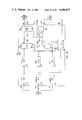
FIGS. 1 and 2 illustrate, in block diagram form, a communication system utilizing the switching architecture of the present invention;
FIG. 2A functionally illustrates a logical flow of test packets for testing a switching network and its attached trunks and trunk controllers;
FIG. 3 illustrates the contents of a call setup packet which is routed from an originating customer terminal to a destination customer terminal through the switching system;
FIG. 4 illustrates the contents of the call reply packet transmitted from the destination customer terminal to the originating customer terminal in response to the receipt of the call setup packet;
FIG. 5 is a detailed block diagram of switching network 116;
FIG. 6 illustrates a switch packet which is used to route the call setup packet of FIG. 3 from trunk controller 130 to central processor 115 via switching network 116 and trunk controller 129;
FIGS. 7 through 9 illustrate the contents of the switch packet used to transmit the call reply packet of FIG. 4 through switching network 116 as the packet progresses through the different stages of switching network 116 from trunk controller 131 to trunk controller 130;
FIG. 10 is a detailed block diagram of switching node 500-15 of switching network 116;
FIG. 11 is a detailed block diagram of input control 1000 of switching node 500-15;
FIG. 12 is a detailed block diagram of address rotation circuit 1106 of input control 1000;
FIG. 13 is a detailed block diagram of output control 1007 of switching node 500-15;
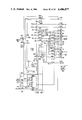
FIG. 14 illustrates, in block diagram form, trunk controller 131;
FIG. 15 illustrates the logical organization of memory 1401 of trunk controller 131;
FIGS. 16 through 26 are detailed block diagrams of subsystems which comprise receiver 1402 of trunk controller 131;
FIG. 27 is a detailed block diagram of address control 1404 of trunk controller 131;
FIG. 28 illustrates the logical operation of address control 1404 in relationship to memory 1401;
FIG. 29 is a detailed block diagram of the implementation of pointers as used in receive interface 2701 of address control 1404;
FIG. 30 is a detailed block diagram of receive interface 2701;
FIG. 31 is a detailed block diagram of switch interface 1418 of trunk controller 131;
FIGS. 32 through 40 are detailed block diagrams of subsystems which comprise input circuit 1406 of trunk controller 131;
FIG. 41 is a block diagram of output circuit 1405 of trunk controller 131;
FIGS. 42 through 44 illustrate packet transformations performed by the subsystems of output circuit 1405 of trunk controller 131 on packets read from memory 1401 of trunk controller 131;
FIGS. 45 through 49 are detailed block diagrams of subsystems which comprise output circuit 1405 of trunk controller 131;
FIGS. 50 through 53 are detailed block diagrams of subsystems which comprise transmitter 1403 of trunk controller 131;
FIG. 54 is a timing diagram; and
FIG. 55 shows the manner in which certain of the figures should be arranged to show the specific illustrative embodiment of the invention.
The drawing shows in FIG. 1 the heavy line blocks of switching network 116, central processor 115, trunk 118, and trunk controllers 129, 130, 131, and 140 for emphasis of the principal building blocks of the present invention.
FIGS. 1 and 2 show an illustrative packet switching system having a plurality of local offices 102, 103, 108 and 109, and a plurality of toll offices 104-107 serving a plurality of customers such as customers 100 or 110. The following description first presents a general description of the subsystems comprising the packet switching system of FIGS. 1 and 2. Then, a brief resume of the functional operations of a switching network, central processor, trunk, and trunk controllers in the transmission of test packets for testing of the switching system is given to provide a focus on the invention. Next, a description is presented of the manner in which a packet transmitted from a customer 100 resident interface 127 to customer 110 resident interface 155 has the necessary self-routing information inserted into it by each trunk controller in its route through the packet switching system. Once the routing of the packet through the switching system has been described, the procedure used to compile the routing information is then described; and then, the method used to store this information in each trunk controller in the route is described. Finally, a detailed description of each block of FIG. 1 and 2 is given.
As shown in FIG. 1, local office 102 comprises a switching network 116 which terminates a plurality of trunk controllers and which cooperates with central processor 115 via a central processor trunk controller 129 which is also connected to the switching network. Each trunk controller is tied into the network by unilateral transmission media. Trunk controller 131, for example, receives information from switching network 116 via conductor 132 and transmits information to switching network 116 via conductor 133.
On the customer side of local office 102, the local office is connected to customers via concentrators which are interconnected to the switching network via trunk controllers. A concentrator has an internal switching architecture similar to that of switching network 116 which is described in greater detail later and has a self-contained trunk controller which interfaces the concentrator to the attached trunk. The concentrator's trunk controller is similar to trunk controller 131 which is described in greater detail later. Each concentrator has connected to it a microprocessor which is used in conjunction with the attached access line controller to perform the initial call setup sequences and to provide call supervision as a supplement to the inherent self-routing characteristics of the packets being transmitted through the packet switching system. The customer units are connected to the concentrators by the access line controllers. Each access line controller stores logical address and control information which is stored in the access line controller by the controlling microprocessor. This logical address information is used to control the first portion of the route taken by the packets transmitted through the attached switching network via the interconnecting trunk controller. Each access line controller is connected to a resident interface contained within each customer unit via standard bilateral transmission media. Packets are transmitted between the access line controllers and the resident interfaces using standard packet protocols which define three virtual channels for communication between the resident interface and the access line controller.
Each trunk controller comprises a memory containing a translation table for converting the logical addresses into switch addresses which are used by the switching network to route the packets to the destination trunk controller. Switching network 116 is interconnected to toll offices such as 104 by high speed trunks with each trunk being terminated on both ends by a trunk controller. The subject matter of FIG. 1 is substantially duplicated in FIG. 2.
Turning now to FIG. 2A, a logical flow of test packets for the testing of switching network 116, trunk controllers 130, 131 and 140, and trunk 118 is explained. Route 200 of FIG. 2A illustrates the routing of a packet used to test a path through switching network 116 between any two trunk controllers. In order to transmit a packet over route 200, central processor 115 assembles a switch test packet having an address field designating trunk controller 130 and addresses designating trunk controller 131 and processor 115 contained in the data field of the packet. Details concerning routing of this packet and the manner in which the circuitry of the various trunk controllers respond to the packet is given in the discussion of FIG. 14. Processor 115 transmits the assembled test packet through network 116 to controller 130. Upon receipt of the packet, trunk controller 130 performs an error check to determine whether or not an error has occurred during transmission of the packet, reads the address designating controller 131 from the data field, inserts this address into the address field of the packet, and then retransmits that packet through network 116 to controller 131. Upon receipt of the packet, controller 131 checks to determine if an error occurred during the transmission of the packet from controller 130, reads the address designating processor 115 from the data field, inserts that address into the address field of the packet, and retransmits the packet back to processor 115 via network 116. The routing of the switch test packet along route 200 is entirely determined by information within the switch test packet, and no preconditioning of the trunk controllers is required by processor 115.
In order to test a trunk interconnecting two networks, a central processor transmits a test packet over the connecting trunk and effects the loop back of that test packet from the distant trunk controller to the central processor. Such a test route is illustrated by route 201 in FIG. 2A for testing trunk 118. Processor 115 assembles a trunk test packet which is transmitted through network 116 to controller 131. The latter is responsive to the packet to perform an error check and to transmit this packet over trunk 118 to controller 140. Upon receipt of the trunk test packet, controller 140 performs an error check and retransmits the trunk test packet back to controller 131 via trunk 118. Controller 131 is responsive to the loop back trunk test packet to transmit the latter to processor 115 via network 116 after performing an error check. Since processor 115 can transmit packets which are looped back from the distant trunk to any trunk, processor 115 can test any trunk attached to network 116.
Turning now from the testing functions, the procedure for obtaining and storing self-routing information in address memories of the appropriate address line controllers and trunk controllers is described. The information is obtained by a call setup packet being transmitted from the appropriate access line controller connected to the originating customer unit through the various microprocessors and central processors which are associated with the different concentrators and local and toll offices which form the route through which the call setup packet must transverse in order to reach the destination customer unit. As the call setup packet progresses along this route, each processing entity inserts a new logical address into the packet and stores the necessary logical and switch address information in the appropriate access line controller or trunk controllers. Once the call setup packet is received at the microprocessor attached to the concentrator to which the destination customer unit is connected via an access line controller, the receiving microprocessor transmits the appropriate logical and switch address information to the connected access line controller which stores it in its address memory; and the receiving microprocessor assembles and transmits a call reply packet which indicates that the call has been properly set up. After the call reply packet is received by the originating customer access line controller, all the necessary routing information is set up in the access line controllers and trunk controllers forming the packet route so that packets can be directly routed through the switching networks without the packets having to be handled by the associated processing entities.
The utilization of the call setup packet is now illustrated in greater detail by describing the establishment of a telephone call between customers 100 and 110. Customer 100 calls customer 110 by dialing the customer 110 telephone number. Resident interface 127 collects the dialed digits in the conventional manner. After resident interface 127 has collected the dialed digits, it transmits the dialed digits in a packet via line 122 to access line controller 112a. In response to the packet received from resident interface 127, access line controller 112a assembles and transmits the packet shown in FIG. 3 to microprocessor 111 via concentrator 112. The packet identifier field identifies this packet as a signaling packet and a "1" in the most significant byte of data field indicate that the packet is a call setup packet. The remainder of the data field contains the dialed telephone number.
Upon receipt of the packet of FIG. 3, microprocessor 111 examines the dialed telephone number and determines that a connection is required through switching network 116. First, microprocessor 111 transmits to access line controller a new logical address to be used in subsequent packets and the switch address defining concentrator 112's trunk controller which connects trunk 117 to concentrator 112. This switch address is used by concentrator 112 to route subsequent packets to trunk 117. Next, microprocessor 111 stores in concentrator 112's trunk controller the switch address identifying access line controller 112a and information defining the virtual channel to be used by access line controller 112a in communicating with resident interface 127. Finally, microprocessor 111 assembles a packet similar to the one shown in FIG. 3, but having the logical address in the logical address field which had been stored in the address memory of access line controller 112a. This new packet is then transmitted to central processor 115 via concentrator 112, trunk 117, trunk controller 130, switching network 116, and trunk controller 129.
Upon receipt of the packet from microprocessor 111, processor 115 determines from the dialed telephone number by performing a table look-up operation that the call must be sent through to office 104. Processor 115 first transmits the logical address contained in the received packet and the switch address identifying trunk controller 130 to trunk controller 131. Trunk controller 131 stores this address information in an internal memory and uses this information to perform the necessary logical to switch address translation on subsequent packets associated with the call being set up. Processor 115 then transmits to trunk controller 130 a new logical address and the switch address identifying trunk controller 131. This address information is used to perform the necessary logical to switch address translation for routing packets from trunk controller 130 to trunk controller 131 associated with the call being set up through switching network 116. The last operation performed by processor 115 is to transmit a call setup packet similar to that shown in FIG. 3 to central processor 113 via switching network 116, trunk controller 131, trunk 118, trunk controller 140 and switching network 146. The packet transmitted to processor 113 has in the logical address field the logical address information identical to that previously stored in trunk controller 130.
Upon receipt of the packet from trunk 118, processor 113 performs operations in response to this packet similar to those performed by processor 115 as previously described with respect to the call setup packet. Processor 113 then transmits a call setup packet to central processor 123 via switching network 146, trunk controller 142, trunk 119 trunk controller 147, and switching network 148. Processor 123 performs similar operations to those performed by processor 113 and transmits a new call setup packet to central processor 114 via switching network 148, trunk controller 149, trunk 120, trunk controller 150, and switching network 151. Upon receipt of the call setup packet from processor 123, central processor 114 stores the logical address information of this packet and the switch address designating trunk controller 150 in trunk controller 141. Central processor 114 then transmits a new logical address and the switch address designating trunk controller 141 to trunk controller 150, which stores this information. After storing the necessary information in trunk controllers 141 and 150, processor 114 assembles a new call setup packet having the logical address which had previously been stored in trunk controller 150 in the logical address field and transmits this call setup packet to microprocessor 125 via switching network 151, trunk controller 141, trunk 124, and concentrator 126.
Upon receipt of the call setup packet from processor 114, microprocessor 125 reads the logical address information contained in the logical address field and stores the logical address in address memory 152 of access line controller 126a. Microprocessor 125 then transmits a call reply packet as illustrated in FIG. 4 to microprocessor 111 via the previously defined route through the packet switching systems of FIGS. 1 and 2. The logical address field of the packet of FIG. 4 contains the logical address which microprocessor 125 received in the call setup packet from processor 114. Trunk controller 141 is responsive to the receipt of the packet of FIG. 4 to translate the contents of the logical address field using the previously stored logical address to switch address translation information and to insert the previously stored logical address into the call reply packet. The switch address which results from this translation by trunk controller 141 designates trunk controller 150. This switch address is used by switching network 151 to route the call reply packet to trunk controller 150. Trunk controller 150 is responsive to receipt of the call reply packet to transmit this packet to trunk controller 149 via trunk 120. The call reply packet is similarly routed through the various trunk controllers until it is received by microprocessor 111. Once the call reply packet is received by microprocessor 111, all the necessary information for routing calls through the various switching networks is stored within the trunk controllers and access line controllers in the route.
The network itself comprises three stages of switching nodes. The first stage comprises nodes 500-0 through 500-15, the second stage comprises switching nodes 501-0 through 501-15, and the third stage comprises switching node 502-0 through 502-15. Transmission through the network is from left to right. Each switching node is a packet switch. Each packet switch has four inputs and is capable of buffering one packet on each input. The packets received on any input are transmittable on any of the four output terminals of the packet switch. After receipt of a packet on an input terminal, the address contained in that packet is used to determine which output terminal should be used to retransmit the packet. Only the two most significant bits of the address are used to designate the output terminal for a particular switching node. For example, switching node 500-12 retransmits the packet on line 505 if the most significant bits are equal to zero, on line 506 if the most significant bits are equal to one, on line 507 if the most significant bits are equal to two, and on line 508, if the most significant bits are equal to three.
Each node properly rearranges the address bits so that the receiving switching node in the next stage has the correct bits in the most significant bit positions in order to determine which output terminal should be used to retransmit the packet at that stage.
The operation of switching network 116 as shown in FIG. 5 can be better understood by considering the example of the switching of the packet shown in FIG. 3 through this network to central processor 115. The packet shown in FIG. 3 is transmitted by microprocessor 111 via trunk 117 to switching network 116. Upon receipt of the packet shown in FIG. 3, trunk controller 130 forms a new packet which is illustrated in FIG. 6.
The new packet is formed by taking the original packet received from trunk 117, removing the flags and stuffed bits, and then adding the new fields of start bit, packet length, destination trunk controller, source trunk controller, control, arrival time, and a new CRC field. Trunk controller 130 responds to the packet identifier containing a "0" by inserting a "0" into the destination trunk controlled field. This is the trunk number for trunk controller 129 to which central processor 115 is connected. Trunk controller 130 inserts its own output connection number on switching network 116 (in this example 48) into the source trunk controller field. The start bit defines the start of the network packet and the packet length defines the length of the network packet. Trunk controller 130 inserts into the arrival time field the relative time of day. Once the packet of FIG. 6 has been formed and the input 513 of node 500-12 is idle, trunk controller 130 transmits this packet to node 500-12.
Node 500-12 examines the most significant bits of the address field and selects output 505 since these bits are zero. Before transmitting the packet to node 501-12 via output terminal 505, node 500-12 rotates the address field two bits to the left; this results in the two most significant bits becoming the least significant bits, and the two middle bits of the address field shown in FIG. 6 becoming the two most significant bits.
Node 501-12 examines the address field upon receiving it and selects output 512 since the most significant bits are zero. Node 501-12 also rotates the address field two bits to the left. Node 501-12 transmits the packet to node 502-0 via the output terminal 512. Upon receipt of the packet, node 502-0 examines the address field and selects output terminal 514 since the two most significant bits of the address are zero. Upon receiving the packet, trunk controller 129 strips off the start bit, network address field, and network packet length, and transmits to central processor 115 the packet identifier, logical address, time stamp, and data fields plus a recalculated CRC field.
A second example will be used to help illustrate the operation of switching network 116 as shown in FIG. 5. This will be done by following the transmission of the packet shown in FIG. 4 through switching network 116 from trunk 118 to trunk 117. Upon receipt of the packet shown in FIG. 4, trunk controller 131 forms the packet shown in FIG. 7. After forming this packet, trunk controller 131 transmits this packet to switching node 500-15 via input terminal 515. Switching node 500-15 examines the two most significant bits of the network address field (in this example a binary three), and selects link 516 to transmit the packet shown in FIG. 7. Before switching node 500-15 starts to transmit the packet via link 516, switching node 500-15 performs a left rotate operation on the network address field, and the result is the packet shown in FIG. 8. Upon receiving the packet from switching node 500-15, switching node 501-15 examines the two most significant bits of the network address field as shown in FIG. 8 and selects output 517 to transmit the packet out. Before transmitting the packet, switching node 501-15 performs a left rotate operation on the packet, resulting in the packet shown in FIG. 9. Upon receiving the packet of FIG. 9, switching node 502-12 responds to the network address field by transmitting the packet to trunk controller 130 via conductor 135. Switching node 502-12 also performs the left rotate operation on the network address field. The packet that is transmitted to trunk controller 130 via conductor 135 is identical to the packet shown in FIG. 9 with the network address field rotated. Trunk controller 130 forms a new packet which is identical to that shown in FIG. 9 with the exception that the start bit, network packet length, destination trunk controller, source trunk controller, control, and arrival time fields have been eliminated, a new CRC field has been calculated and inserted, and the time stamp field has been updated. Trunk controller 130 then retransmits this new packet on trunk 117.
It would be obvious to one skilled in the art to expand network 116 as shown in FIG. 5 to be capable of terminating more trunks by the addition of more switching nodes. In addition, it would be obvious to one skilled in the art to use such a switching network to correctly interconnect several pieces of digital equipment such as computers or terminals. The other switching networks and concentrators shown in FIG. 1 and 2 are similar in design to switching network 116.
Switching node 500-15 is illustrated in greater detail in FIG. 10. The other switching nodes are identical in design to switching node 500-15. The switching node consists of four input controls which can transmit information to any one of four output controls. The input controls 1000 through 1003 are connected to the output controls 1004 through 1007 via cables. For example, input control 1000 is connected to output control 1007 via cable 1008. Cable 1008 comprises three conductors 1009, 1010, and 1011. The other interconnecting cables on FIG. 10 are identical in design to cable 1008.
When input control 1000 has a packet to transmit to output control 1007, it transmits a request signal via conductor 1010 to output control 1007. Input control 1000 continuously transmits this request signal until the entire packet has been transmitted to output control 1007. When output control 1007 is free to receive information from input control 1000, output control 1007 transmits a grant signal via conductor 1011 to input control 1000. Upon receipt of the grant signal, input control 1000 commences to transmit the packet to output control 1007 via conductor 1009.
For example, the packet shown in FIG. 7 would be transmitted through switching node 500-15 as illustrated in FIG. 10 in the following manner. When input control 1000 recognizes the start bit, it has already received not only the start bit but also the two most significant bits of the network address. Input control 1000 decodes the two most significant bits of the network address field and determines that the packet was to be transmitted to output control 1007 via cable 1008. Input control 1000 requests permission to start transmission via conductor 1010; and when output control 1007 returns the grant signal via conductor 1011, input control 1000 starts the transmission of the packet to output control 1007 via cable 1008. Before transmitting the network address field, input control 1000 left rotates this address two bits so that the network address transmitted is that shown in FIG. 8. Upon receipt of the start bit of the packet, output control 1007 starts to retransmit this packet out on link 516.
The operation of input control 1000 will now be further explained by using the previous example which dealt with the transmission of the packet shown in FIG. 7. Input shift register 1100 is continuously being clocked by system clock 161 via conductor 1111. As data is received via input terminal 515, it is clocked through input shift register 1100. Once the start bit reaches bit position 10 of input shift register 1100, controller 1104 detects this bit and transmits a pulse on conductor 1113. This pulse causes length register 1102 to store the network packet length field, and causes address register 1101 to store the two most significant bits of the network address field, which are contained in bit positions 0 and 1 of input shift register 1100.
The operation of output control 1007 as shown in FIG. 13 will be explained in greater detail by considering the previous example of input control 1000 transmitting a packet of data to output control 1007 vra cable 1008. When input control 1000 transmits the request signal via conductor 1010, control circuit 1300 transmits the grant signal to input control 1000 via conductor 1011 if the link 516 is not being used by one of the other input control circuits and the output of flip-flop 1301 is set. Assuming that flip-flop 1301 was set, control circuit 1300 transmits the grant signal to input control 1000 and conditions data selector 1303 via a cable 1308 to select the data being transmitted on conductor 1009 and retransmit this data on conductor 1307. In addition, control circuit 1300 enables the tri-state device 1302 to transfer the information on conductor 1307 to link 516.
After input control 1000 has transmitted the entire packet, it removes the request signal from conductor 1010. Once the request signal is removed from conductor 1010, control circuit 1300 sends a reset signal to flip-flop 1301 via conductor 131O and stops transmitting signals via cable 1308 and conductor 1309. Once the input control of the switching node 501-15 is capable of accepting another packet, it transmits the open link signal via conductor 1306, tri-state device 1311, and link 516. The open link signal sets flip-flop 1301 via the S input. Once flip-flop 1301 is set, control circuit 1300 can once again respond to request signals from the input controls.
Consider an example where normal data packets are transferred from trunk 118 to switching network 116. Incoming packets, similar to those shown in FIG. 3, are received by receiver 1402 in a serial fashion at a 1.544 Mb/s rate. Receiver 1402 adds the arrival time to the packet, and transforms the serial information into a byte. Once it has assembled a byte, it transmits a write request, via control bus 1408, to address control 1404. Receiver 1402 then writes the byte into memory 1401 via data bus 1407 and address control 1404. The location in memory 1401 that the byte is written into is designated by the address pointers associated with receiver 1402. This process continues until receiver 1402 has transferred an entire packet into memory 1401. After receiver 1402 has transmitted an entire packet, it transmits an end of packet signal, via control bus 1408, to address control 1404. Address control 1404 then transmits a packet available signal, via control bus 1412, to output circuit 1405. This packet available signal is transmitted as long as there is a complete packet in memory 1401.
Consider another example where packets are transferred from switching network 116 to trunk 118. Packets from switching network 116 are received by input circuit 1406 via switch interface 1418. Input circuit 1406 forms this data into bytes. It then sends a write request via control bus 1414, and sends the packets via data bus 1413 to address control 1404. Address control 1404 writes the information into memory 1401, via memory address bus 1417, memory data bus 1415, and memory control bus 1416. When an entire packet has been stored in memory 1401, input circuit 1406 transmits an end of packet signal to address control 1404 via control bus 1414. Address control 1404 then transmits a packet available signal to transmitter 1403 via control bus 1410. Transmitter 1403 makes a read request to address control 1404, and receives the packets via data bus 1409. Transmitter 1403 transforms the packets into packets similar to those in FIG. 4, and transmits them to trunk 118 at a 1.544 Mb/s rate. Transmitter 1403 also performs error checking, and recalculates the CRC field. In addition, transmitter 1403 updates the time stamp field of the packet. It does this by subtracting the arrival time from the present time, and adding this difference to the time stamp field.
FIG. 15 illustrates the four packet buffers, and logical channel translation table contained in memory 1401. Packets arriving from receiver 1402 are written into either receive buffer 1501 or trunk test buffer 1502. Trunk test buffer 1502 is reserved for test packets that are to be looped back over the trunk. All other arriving packets are sent to receive buffer 1501. Packets arriving from input circuit 1406 are written into either transmit buffer 1503 or switch test buffer 1504. Transmit buffer 1503 is for packets that are to be transmitted on the trunk via transmitter 1403. Switch test buffer 1504 is for switch test packets, and for memory read and write packets. Logical translation table 1505 contains the logical to physical address translation information received from the central processor via memory write packets.
The reading and writing of the circular buffers in memory 1401 is controlled by read and write pointers, located in address control 1404. These read and write pointers point to the specific memory locations within the various buffers. Read or write pointers are provided for receiver 1402, transmitter 1403, input circuit 1406 and output circuit 1405. These pointers are used to read or write the various circular buffers, depending on the circuit. The structure is as follows: Receive circuit--receive buffer and trunk test buffer write pointers; output circuit--receive buffer and switch test buffer read pointers; input circuit--transmit buffer and switch test buffer write pointers; transmit circuit--transmit buffer and trunk test buffer read pointers.
In addition to the various read and write pointers, address control 1404 also contains temporary pointers. Receiver 1402 has access to one temporary pointer, which is used to save the value of the write pointer. At the beginning of each packet write operation, the temporary pointer is set to the same address as the write pointer. If an error is discovered while the packet is being written, the write pointer is set back to the address of the temporary pointer. In this way, the packet containing an error is overwritten, effectively discarding it. Input circuit 1406 has access to two temporary pointers. One is used to save the value of the write pointer. The other temporary pointer is used during memory write operations, and will be discussed later. Output circuit 1405 has access to one temporary pointer, which is used during memory read operations.
The following description shows the packet flow of an ordinary data packet from the trunk to the switch network. Receiver 1402 receives trunk packets, and pads the trunk packets with zeroes, in order to provide space in the packet to transform the trunk packets into switch packets. Once receiver 1402 has done this, it makes a write request to address control 1404, in order to write the packet into receive buffer 1501 in memory 1401. Address control 1404 receives the write request and makes the receive buffer write pointer available. Receiver 1402 then writes the packet into receive buffer 1501 at the address specified by the write pointer. Address control 1404 then sends a packet available signal to output circuit 1405, causing output circuit 1405 to send a read request to address control 1404. Address control 1404 makes the receive buffer read pointer available, allowing output circuit 1405 to read receive buffer 1501 at the address specified by the read pointer. Output circuit 1405 reads the packet, modifies the necessary fields to convert the trunk packet into a switch packet, performs the necessary logical to physical address translation, and sends the packet to the switching network. The logical to physical address translation involves reading the logical translation table in memory 1401, and updating the required packet fields.
The packet flow of an ordinary data packet from the switch network to the trunk is as follows. The packet is received from the switching network via switch interface 1418, and is sent to input circuit 1406. Input circuit 1406 makes a write request to address control 1404, in order to write the packet into transmit buffer 1503 in memory 1401. Address control 1404 receives the write request and makes the transmit buffer write pointer available. Input circuit 1406 then writes the packet into transmit buffer 1503, at the address specified by the write pointer. Address control 1404 then sends a packet available signal to transmitter 1403, causing transmitter 1403 to send a read request to address control 1404. Address control 1404 makes the transmit buffer read pointer available, allowing transmitter 1403 to read transmit buffer 1503 at the address specified by the read pointer. Transmitter 1403 makes a read request to address controller 1404, in order to read the packet from transmit buffer 1503. Once transmitter 1403 has read the packet, it removes the header information from the packet, which transforms the packet into a trunk packet. Transmitter 1403 then transmits the packet on the attached trunk.
Trunk test packets are received by receiver 1402 from the trunk. They are written into trunk test buffer 1502 in memory 1401, using the trunk test buffer write pointer in address control 1404. This operation is similar to the operation of the receive buffer write pointer. Transmitter 1403 then makes a read request to address control 1404, in order to read trunk test buffer 1502, using the trunk test buffer read pointer. Once transmitter 1403 has read the test packet, it transmits it back to the trunk. Switch test packets are processed in a similar manner. They are received by input circuit 1406, which writes them into switch test buffer 1504 in memory 1401, using the switch test buffer write pointer. Output circuit 1405 then reads switch test buffer 1504, using the switch test buffer read pointer in address control 1404. Once it has read the packet, it sends it to the specified trunk controller via the switch network.
Memory write packets are used to write information into memory 1401. This information includes the logical to physical address translations, which are written into logical translation table 1505. Memory write packets are originated by the central processor, and are sent to input circuit 1406, which writes part of the packet into switch test buffer 1504, and part of the packet into logical translation table 1505, both located in memory 1401. The portion of the memory write packet that is written into switch test buffer 1504 is written via the switch test buffer write pointer; the portion of the packet that is written into logical translation table 1505 is written via the second input circuit temporary pointer, both located in address control 1404. Output circuit 1405 then reads the information stored in switch test buffer 1504, and reads the logical translation information. It then assembles these two portions of data into a packet that is identical to the original memory write packet, and transmits this packet back to the central processor.
Memory read packets are originated by the central processor, and are used to allow the central to read portions of memory 1401. The incoming memory read packet contains the memory address, and the number of bytes to be read. Output circuit 1405 reads memory 1401 at the address specified in the packet, and inserts the number of bytes specified into the memory read packet. It then returns the packet (containing the requested data) to the central processor.
Trunk and switch packets are further described with respect to the fields contained in each of these two packet types. The actual packet manipulation and conversion details are described later. Trunk packets carry data and maintenance information between the trunk equipment and the trunk controllers. The format of a typical trunk packet is shown in FIG. 3. An explanation of the fields is given in the following paragraphs.
The flag field is a unique bit pattern (01111110) used to identify the beginning and end of a packet. The packet identifier (PID) field determines whether the packet is for signaling, testing, or the transmission of normal data. A "0" in this field indicates a signaling packet used for call set-up. As previously described, this packet is routed through all central processors along the path, in order to establish the path that all subsequent packets will take for the duration of the call.
A PID field of "1" indicates a signaling packet that sends signaling information over a path that has already been established. This packet type is read only at the terminating central office.
A PID field of "2" or "3" is a test packet, which is used to test a trunk in the network. The originating central processor sends a test packet to one of its trunk controllers, via the switching network. This packet is indicated by a PID field of "2". The packet is transmitted by the first trunk controller over the trunk to a second trunk controller. Since the PID field is a "2", the second trunk controller changes the field from a "2" to a "3" and loops the test packet back to the first trunk controller over the trunk. The first trunk controller receives the packet, and reads the PID field. Since the PID field is a "3", the first trunk controller returns the packet to the central processor.
A PID field of "8" through "11" identifies the packet as one carrying normal data. The ascending order of numbers indicates levels of flow control. An "8" indicates no flow control. The numbers "9" through "11" indicate increasing levels of flow control. When flow control increases, the originating office sends the packets out with a greater amount of time in between. This is to prevent system overload due to increased traffic.
A PID field of "12" indicates a datagram. This is a single packet that carries a complete message. A datagram is routed as follows. A datagram is created by the central processor associated with the terminal equipment sending the datagram. The datagram is then routed to each central processor in the network that the datagram passes through. Each central processor reads the logical address field of the datagram to determine the next central processor to which the datagram is sent. Once the datagram reaches the destination central processor, the destination central processor routes the datagram to the destination customer's terminal equipment. The address information is not retained because a path is not required to send additional packets.
The logical address field is used to derive the address of the destination trunk controller. This is done by the current trunk controller using the logical address to index logical translation table 1505 contained in memory 1401. Logical translation table 1505 contains the number of the next trunk controller and the new logical address. The current trunk controller inserts the new logical address into the packet's logical address field and then routes the packet. The time stamp field carries the accumulated time that it takes for the packet to travel through the switch system. This field is updated in conjunction with the arrival time field, which is inserted when the packet is first received from the trunk. When the destination trunk controller receives a packet, it calculates the difference between the arrival time and the present time, in order to update the time stamp field. The data field contains the actual data, or information, that the packet is to carry. In addition, this field carries certain high level protocol information. The cyclic redundancy code (CRC) field is used for error detection. This field is generated by the transmitting trunk controller, and tested by the destination trunk controller, in order to determine if the packet contains errors.
Switch packets carry data and maintenance information within the switching network. The format of a typical switch packet is shown in FIG. 6. A data type switch packet contains all the fields contained in a trunk packet, and in the same order. The one exception is the two flag fields, which are not contained in the switch packet. Also, the CRC field is recalculated and checked at several stages of the transformation process from trunk packets to switch packets. An explanation of the fields unique to switch packets is provided in the following paragraphs.
The packet length field is the total length of the packet, in bytes. This field is computed by receiver 1402. The destination trunk controller (DTC) and source trunk controller (STC) fields are used for packet routing. The DTC is the address of the destination trunk controller and is obtained from logical translation table 1505. The STC field is the address of the trunk controller that is presently handling the packet.
As given in the following Table 1, the control field, CNTL, defines the type of switch packet.
TABLE 1 ______________________________________ SWITCH PACKET TYPE CNTL EXPLANATION ______________________________________ 0Standard data packet 1 Maintenance readpacket 2Maintenance write packet 3 Memory readpacket 4Memory write packet 5 Test packet-routed tofirst trunk controller 6 Test packet-routed to second trunk controller ______________________________________
Standard data packets carry the information contained in data type trunk packets (packet identifier of "8", "9", "10", or "11"), as well as signaling and datagram packets (packet identifier of "0", "1", or "12") through the switch network. These packets are transformed back to trunk packets by the next trunk controller in the network, and then transferred back to switch packets, as required, for transmission through subsequent switch networks. Maintenance information is transmitted through the system with maintenance write and maintenance read packets. These packets give the central processor the ability to read and write maintenance information into the trunk controller. This maintenance information includes error and control information. A maintenance write packet is generated by the central processor and is sent to the appropriate trunk controller. Once this packet arrives at the trunk controller, the trunk controller examines the control field, determines that it is a "2" (indicating a maintenance write) and writes the data portion of the packet into maintenance register 3101 in switch interface 1418.
When the trunk controller receives a switch packet with at "1" in the control field, it performs a maintenance read operation. The data in the maintenance register is read, and stored in the data portion of a packet. The packet is then transmitted to the originating central processor.
Switch packets are also used to read and write the memory portion of the trunk controller. In a memory write operation, the switch packet's control field is a "3". Input circuit 1406 receives the packet from the central processor, writes the data portion into the requested location in memory 1401, and writes the rest of the packet into switch test buffer 1504. Output circuit 1405 reads the data from the specified location in memory 1401, and reads the remainder of the packet from switch test buffer 1504. It then assembles a new packet from these two segments, and transmits the new packet back to central processor 115 via switching network 116.
A test packet is a type of switch packet that can route test data through two trunk controllers, before routing the packet back to the central processor. When the test packet arrives at the first trunk controller, the control field is set to "5". This indicates that the packet is to be routed to a second trunk controller before being returned to the central processor. Before leaving the first trunk controller, output circuit 1405 changes the control field from a "5" to a "6", and then sends the packet to the second trunk controller. The address of the second trunk controller is specified in the data field. After the second trunk controller receives the test packet, it reads the control field. Since the field is a "6", the second trunk controller routes the packet directly to the central processor.
The main function of receiver 1402 is to convert trunk packets, received from the trunk side of the network, into switch packets, which are then transmitted through the switching part of the network. The conversion consists of (1) removing the start and end flag fields, and (2) adding fields at the beginning of the packet. The transformation also requires that the CRC field be recalculated. The added fields are as follows. The first two added fields, destination trunk controller and source trunk controller are filled with zeroes. The actual source and destination trunk controller values are added by output circuit 1405 after it reads the packet from receive buffer 1501. The next added field is the control field. The last added field is the arrival time field. This field is filled in with the actual time that the packet arrives at receiver 1402, and is used by the destination trunk controller to update the time stamp field.
During packet conversion, the destination trunk controller, source trunk controller and control fields are initialized to zero. The arrival time field is initialized to the arrival time of the packet (expressed as a negative number). The packet identifier field is unchanged, with one exception: if the packet identifier field of the incoming packet is a "2", rndicating a test packet, it is changed to a "3", indicating a trunk test packet that is returning. As already mentioned, the CRC field is updated; however, the updating process has this complication. The CRC field is computed as though the packet length field contained all zeros, and the actual length of the packet was contained in a separate field between the data and CRC fields. The reason for this is because the length of the packet is being computed as the packet comes in, and is not known until the entire packet is received.
The trunk packets are received by flag removal and bit unstuffing circuit 1601 on conductor 1604. This circuit detects the start and end points of each packet by detecting the presence of the start and stop flags contained in the packet. Once the flags are detected, they are removed. In addition, this circuit performs bit unstuffing. Bit unstuffing is the removal of bits that were placed in the bit stream to ensure that the flag pattern does not occur at any place other than the start and end of the packet.
Flag removal and bit unstuffing circuit 1601 sends the packets to packet reformatter 1602 via conductor 1605. A signal is placed on conductor 1606 when the packet first arrives at packet reformatter 1602. This signal remains as long as the packet is being processed. A similar signal is present on conductor 1609 during the time that the packet is being transferred from packet reformatter 1602 to serial to parallel converter 1603. A "1" is placed on conductor 1607 during every clock pulse that conductor 1605 contains data. Packet reformatter 1602 receives the trunk packet from 1601 and adds the appropriate fields to allow the forming of a switch packet. In addition, this circuit performs error detection, and modifies the PID field as required.
Error detection is done by checking the CRC field of each incoming packet. If an error is detected, 1602 transmits an error signal to 1603 via conductor 1612, which causes the packet containing the error to be aborted. Packet reformatter 1602 also detects hardware errors. If a hardware error is found, it is indicated by a signal on conductor 1626.
The PID field modification performed by 1602 is with respect to trunk test packets. An incoming test packet has a PID of "2"; 1602 changes the field to a "3". Additionally, when a test packet is received, 1602 causes conductor 1611 to go high. This causes serial to parallel converter 1603 to write the contents of the test packet into trunk test buffer 1502. Packet reformatter 1602 is fully duplicated and thus is capable of doing fault detection of itself.
Flag removal and bit unstuffing circuit 1601 is shown in greater detail in FIG. 17. This circuit does flag removal and bit unstuffing. Flag removal is performed as follows. A flag pattern of 01111110 is continuously sent over conductor 1604 whenever the trunk is idle. This 8-bit pattern is read into register 1701. At the same time that register 1701 is receiving the bit pattern, register 1702 is receiving a steady stream of "l's" at the same bit rate. After a complete 8-bit flag pattern is received, register 1702 is cleared via a "1" on the output of AND gate 1706, which decodes the presence of the flag pattern. This prevents the "l's", which are being clocked into register 1702, from being sent out of register 1702. The "l's" coming out of register 1702 are routed to AND gate 1714 and register 1705. When "1's" are present, actual data is allowed to flow out of register 1701, and conductor 1607 is activated to signal this actual data.
After a flag pattern from an actual packet is clocked into register 1701, the subsequent bits are actual packet contents rather than the flag pattern. After eight bits of actual data have been clocked into register 1701, AND gate 1706 does not clear register 1702 because the AND gate is not detecting the flag pattern. This causes register 1702 to send a continuous stream of "l's" to one input of AND gate 1714. The other input of AND gate 1714 is receiving the actual packet contents from register 1701. AND gate 1714 is thus enabled by the "l's" coming out of register 1702. Because of the enable signal, the contents of register 1701 are allowed to be shifted into register 1703. Thus, the output of AND gate 1714 is "1" only when the actual packet contents contain a "1". In this way, the packet contents minus the flags are shifted through register 1703 and are sent to packet reformatter 1602 via conductor 1710.
Bit unstuffing is required because whenever transmitter 1403 detects five sequential "l's", it always stuffs a "0". This is so that the packet data never contains the flag pattern. These stuffed zeros are removed by flag removal and bit unstuffing circuit 1601 after the flags have been removed. Bit unstuffing is done as follows. The packet data coming out of AND gate 1714 still contains the stuffed "O's". If a pattern of 11111 is clocked into register 1703, the next bit has to be a stuffed bit, which must be removed. This 11111 pattern causes the output of NAND gate 1718 to go to "0" during the one bit time that the stuffed "0" is in the first position of register 1703. This "0" is shifted through register 1704 at the same time that the actual packet data is shifted through register 1703. When the "0" in register 1704 reaches the input of AND gate 1708, conductor 1606 goes to "0" for that one clock pulse that the stuffed "0" is present in register 1703. Conductor 1606 is the bit present indicator, which is passed to packet reformatter 1602. Since the bit present signal is absent for any clock pulse that a stuffed "0" is contained in register 1703, the stuffed "0" is removed.
Serial to parallel converter circuit 1603 is shown in greater detail in FIG. 24. Serial to parallel converter 1603 comprises buffer 2401 and address control interface 2402. Buffer 2401 receives data, data present and bit present indications from packet reformatter 1602. Buffer 2401 transforms the incoming data into bytes, and sends the bytes to address control 1404 via cable 2720. Address control interface 2402 signals where the information on cable 2720 is to be written by signals on conductors 2721 through 2727. Conductors 2721 through 2723 are write commands for receive buffer 1501, trunk test buffer 1502, and the temporary pointer, respectively. Conductors 2726 and 2727 set the temporary pointer equal to either the receive buffer or trunk test bufter write pointers, and conductors 2724 and 2725 set the receive buffer or trunk test buffer write pointers equal to the temporary pointer.
Receive interface 2701 receives write requests from receiver 1402 on conductors 2721 through 2727; it receives the data from receiver 1402 on cable 2720. Receive interface 2701 responds to these write requests by making either the receive buffer write pointer, trunk test buffer write pointer, or temporary pointer available for writing the data into memory 1401. For example, a signal on conductor 2722 causes receive interface 2701 to write the data into receive buffer 1501, at the address pointed to by the receive buffer write pointer. After the data has been written, the receive buffer write pointer is incremented; this new address and the address plus one are sent to receive buffer full/empty circuit 2704. When receive buffer full/empty circuit 2704 detects that receive buffer 1501 is empty, it resets flip-flop 2705, causing the data present signal to be removed from conductor 2738. If receive buffer full/empty circuit 2704 detects that receive buffer 1501 is overfilled, it sends an overload in receive buffer indication on conductor 2728. A signal on conductor 2722 causes the data on cable 2720 to be written into trunk test buffer 1502. The circuit action is similar to that of writing receive buffer 1501, except that trunk test buffer full/empty circuit 2707 resets flip-flop 2706 when trunk test buffer 1502 is empty, and it indicates that trunk test buffer 1502 is overfilled via a signal on conductor 2729.
The temporary pointer is used for writing the packet length into the length field, and for aborting packets that contain errors. The temporary pointer must be used to write the length because the length field is at the beginning of the packet, and the actual length of the packet is not known until most of the packet has been written into the buffer. The actual length is inserted into the packet in the following manner. The temporary pointer is set equal to the write pointer, and the write pointer starts to write the packet into the buffer. When the packet length (which had been placed near the end of the packet) is ready to be written, it is written using the temporary pointer. Since the temporary pointer had been set equal to the write pointer, it is pointing to the location of the length field. In this way, the actual packet length is written into the length field of the packet.
If an error is detected in the packet, the packet is aborted. This is accomplished by receiver 1402 pulsing conductor 2724, which directs receive interface 2701 to set the write pointer for the receive buffer equal to the temporary pointer.
Overflow conditions are detected by receive buffer full/empty circuit 2704. This is done by 2704 comparing the read pointer against the write pointer plus one. If these two are equal, it indicates that an overflow will occur if the receiver attempts to write another byte into receive buffer 1501.
The operation of input interface 2713 is similar to receive interface 2701. Incoming data is received from input circuit 1406 via cable 2744, and is written into either transmit buffer 1503 or switch test buffer 1504. The write requests from input circuit 1406 are via conductors 2745 through 2752, and conductor 2765. Switch test buffer full/empty circuit 2708 and transmit buffer full/empty circuit 2712 receive write pointer addresses from input interface 2713, in order to maintain the full/empty status of switch test buffer 1504 and transmit buffer 1503. These full/empty circuits reset flip- flops 2709 and 2710, and send buffer overfilled conditions via conductors 2742 and 2743. The operation of transmit interface 2711 is similar to output interface 2703. Data is read from either transmit buffer 1503 or trunk test buffer 1502 in memory 1401. Once the data has been read, it is sent to transmitter 1403 vIa cable 2755. Read requests are received from transmitter 1403 via conductors 2753 and 2754. Transmit interface 2711 contains no temporary pointers.
Temporary pointers are used by receiver 1402, input circuit 1406, and output circuit 1405 for various applications. In the receive circuit, for example, the temporary pointer is used to back-up the write pointer, in cases where the write pointer has written a packet and then receiver 1402 discovers an error. The temporary pointer points to the memory location containing the first byte of the packet. By setting the write pointer equal to the temporary pointer, the packet is effectively aborted.
A typical pointer is shown in FIG. 29. Pointers contain the address of the current position in the buffer in order to read or write the buffer. The pointer circuit does the following: resets the pointer; increments the pointer (including wrap-around); loads the pointer from an external source, for example, setting the read pointer equal to the temporary pointer; and provides the current address, and the address plus one, for use by the full/empty circuit. The current address is stored in register 2901. This address is available on cable 2919; the address plus one is available on cable 2921. A reset operation causes the start address on conductor 2920 to be loaded into register 2901, as follows. The reset is initiated by a signal on conductor 2915. This signal enables register 2901 via OR gate 2902. Additionally, this reset signal operates OR gate 2909, which enables AND gate 2913. The start address on cable 2920 passes through AND gate 2913 and OR gate 2912 to one input of AND gate 2905. The other input of AND gate 2905 is enabled via inverter 2906; thus, the start address is loaded into register 2901. Incrementing the pointer causes the pointer to read or write the next memory address. When the pointer has reached the limit address, incrementing causes wrap around. Incrementing is initiated by a signal on conductor 2916. This signal enables register 2901 via OR gate 2902. The address that is loaded into register 2901 depends on whether or not the limit of memory space has been reached. If the limit has not been reached, comparator 2907 operates, which operates AND gate 2911 and OR gate 2912. When OR gate 2912 operates, the current address plus one is loaded into register 2901 via AND gate 2905 and OR gate 2904. If the limit has been reached. comparator 2908 operates. This operates OR gate 2909, which causes the start address on conductor 2920 to be loaded into register 2901 as previously described. This is the wrap around. Loading from an external source is initiated by a signal on conductor 2917. This signal enables register 2901 via OR gate 2902; additionally, this signal enables AND gate 2903 and disables AND gate 2905 via inverter 2906. When AND gate 2903 is enabled, the external address on cable 2918 is put in register 2901, via OR gate 2904.
Receive interface 2701 is shown in greater detail in FIG. 30. Receive interface 2701 comprises receive buffer write pointer 3001, temporary pointer 3002, and trunk test buffer pointer 3003. These pointers are similar to the pointer described in FIG. 29. and are used to allow receiver 1402 to read receive buffer 1501 and trunk test buffer 1502. Data is received from buffer 2401 on cable 2720, and is written, via cable 3004, into memory 1401 via memory interface 2702. The memory location is specified via address cable 3006. This address is received from the DO lead of the respective pointer 3001, 3002, or 3003) through OR gate 3015 and AND gate 3011. AND gates 3009 through 3011 are multi-input AND gates that send data, write indications, and addresses to memory 1401 via cables 3004 through 3006. Output interface 2703, input interface 2713, and transmit interface 2711 are similar in design to receive interface 2701.
Another maintenance function consists of fault detection circuit 3108 and cables 3110 through 3113. Cables 3110 through 3113 are connected to receiver 1402, transmitter 1403, input circuit 1405, and output circuit 1405, respectively. These cables transmit faults, such as memory error or packet received in error, to fault detection circuit 3108.
Serial to parallel converter 3202 is shown in greater detail in FIG. 38. Serial to parallel converter 3202 comprises buffer 3801 and address control interface 3802. Buffer 3801 receives incoming serial information on conductor 3208 and transforms the information into bytes, which are sent to address control 1404 via cable 2744. Address control interface 3802 signals to address control 1404 where in memory 1401 the data is to be written. This signaling is provided via conductors 2745 through 2752, and conductor 2765. The signaling is done in a manner similar to receive address control interface circuit 2402.
If a packet stored in buffer 3801 contains errors, or if the buffer that the packet is being written into is overfilled, then the packet must be discarded. Packets that contain errors are indicated by a signal on conductor 3211. An overload of transmit buffer 1503 is indicated by a signal on conductor 2743, and an overload of switch test buffer 1504 is indicated by a signal on conductor 2742. The discarding of a packet is done by temporary pointer 1, which is set equal to the write pointer at the start of the write operation. If an error is found or a buffer is overfilled, the write pointer is set equal to temporary pointer, via a signal on conductor 2748 or 2765. The effect of this is to back up the write pointer to the location that the write pointer was at when it began to write the packet. The next packet to be written will overwrite the packet in error, effectively discarding it. This temporary pointer is similar to the temporary pointer for receive interface 2701, shown in FIG. 30. Setting the write pointer equal to temporary pointer 1 is done by control 4028 placing a signal on conductor 4036. This action is done at the end of each write operation. However, during normal write operations when a packet is not to be discarded, the signal on conductor 4036 does nothing because the other input of AND gate 4010 is flop 4013 is reset to "0". This turns off AND gate 4012 which disables the writing of both the transmit and switch test buffers, due to the disabling of AND gate 4016. Additionally, when flip-flop 4013 is reset to "0", AND gate 4010 is enabled, which sets the write pointer equal to temporary pointer 1, and thus discards the packet.
Parallel to serial converter 4101 contains control leads that allow it to access portions of memory 1401 via address control 1404. Access to receive buffer 1501 is provided via conductor 2732. Access to switch test buffer 1504 is provided via conductor 2733. These access leads provide control only; the information contained in memory is transferred to output circuit 1405 via cable 2731. In order to gain access to memory 1401, a signal must be present on conductor 2760. This signal is provided by timer 2714 contained in address control 1404. Output circuit 1405 also contains control leads for the temporary pointer, provided via conductors 2734 through 2737. The temporary pointer is used to perform memory read operations, as specified by memory read and memory write packets.
The packet transformations provided by output circuit 1405 are shown in FIG. 42, FIG. 43, and FIG. 44. The packet configuration going into parallel to serial converter 4101 is the packet as it goes into output circuit 1405. The packet configuration going into packet reformatter 4102 is not an actual packet; rather, it is used to illustrate the intermediate step in the actual packet transformation. The packet configuration coming out of packet reformatter 4102 is the actual packet as it leaves output circuit 1405.
FIG. 42 shows the packet transformation that occurs when a data packet (control field of "0") is read from receive buffer 1501. FIG. 42 is used to illustrate what takes place in the packet when output circuit 1405 reads a data packet. Packet 4201 is the packet as it exists in receive buffer 1501. After parallel to serial converter 4101 receives from address control 1404 a grant signal on conductor 2760, and a data present signal on conductor 2738, it is ready to read receive buffer 1501. This is done by parallel to serial converter 4101 sending a read receive buffer signal to address control 1404 via conductor 2732. This signal causes address control 1404 to read receive buffer 1501 in memory 1401 and to send the data to parallel to serial converter 4101 on cable 2731. This data appears in parallel and is transformed into a serial bit stream. When the logical address of the packet is read, it is loaded into the temporary pointer, via signals on conductors 2735 through 2737. This address is used to access the proper entry in logical translation table 1505, which is inserted into the packet passed from parallel to serial converter 4101 to packet reformatter 4102. The format of this intermediate packet is shown as 4202 in FIG. 42.
After parallel to serial converter 4101 has read receive buffer 1501 and has read the new logical address, it forwards the information to packet reformatter 4102. Packet reformatter 4102 performs two main functions: It changes the order of certain fields of the incoming information so as to place the source and destination trunk controller numbers in their proper fields, and it places the logical channel translation table information into the logical address field. Additionally, packet reformatter 4102 checks the CRC field of the incoming information, and calculates a new length and CRC field. This action results in the actual packet 4203.
FIG. 43 shows the packet transformation that occurs during a memory read (control field of "3") or a memory write (control field of "4") operation. The operations are similar to those for reading a data packet (FIG. 42), with the following exception. In a memory read or memory write, data is read from a memory location specified in the memory read or memory write packet, and the data is placed into the outgoing memory read or memory write packet. At the same time, the remainder of the packet is read from switch test buffer 1504. Packet 4301 is the packet as it exists in switch test buffer 1504. The address field is the memory location of the data that is to be placed in the packet. The count field is the number of bytes of data that are to be read. The packet is read out of switch test buffer 1504 under control of a signal on conductor 2733. When the address field 4304 is read from the buffer, its value is also saved in the temporary pointer. This is done via signals on conductors 4209 and 4210 as previously described for FIG. 42. After count field 4305 is read, the temporary pointer is used to read information from memory 1401. This information is then placed in the data field. Packet reformatter 4102 updates the length, and destination and source trunk controller fields, and recalculates a new CRC field. This forms the actual packet 4303.
The packet transformation for a switch test packet (control field of "5" or "6") is shown in FIG. 44. For a switch test packet transformation, it is necessary to update the destination trunk control field. This is done by using the data in either the trunk control 1 or trunk control 2 fields. For a first hip switch test packet (control field of "5"), the trunk control 1 field is used. For a second hop switch test packet (control field of "6"), the trunk control 2 field is used.
Parallel to serial converter 4101 is shown in greater detail in FIG. 45. This circuit comprises address control interface 4501, and buffer 4502. Incoming packets are sent to both address control interface 4501 and buffer 4502 via cable 2731. Address control interface 4501 is informed of the presence of data in either receive buffer 1501 or switch test buffer 1504 via data present signals on conductors 2738 and 2740. It then controls the transfer of the packets to buffer 4502, which performs the parallel to serial conversion. Address control interface 4501 also controls the reading of the logical channel translation table entries and the data fields of the memory read and memory write packets using the temporary pointer.
The reading of a memorY read or memory write packet (control field of "3" or "4") can be illustrated by also referring to packet 4301 of FIG. 43. Control 4602 receives the "data present in switch test buffer signal" on conductor 2740 and begins to read switch test buffer 1504, as previously described. When the length field appears on cable 2731, it is stored in counter 4603. Counter 4603 begins to count down; when it reaches zero, the packet has been entirely read. When the control field appears on cable 2731, it is decoded by decoder 4601. Once the control field is decoded, it is stored in flip- flops 4605 and 4606. Address control interface 4501 continues to read the packet from switch test buffer 1504. When the address field appears on cable 2731, this address is loaded into the temporary pointer by control 4602 placing a signal on conductors 2735 and 2736. When the count field appears on cable 2731, it is loaded into counter 4603. Counter 4603 then counts the number of data bites that are being read from the memory location specified in the address field. This data is then placed at the end of the packet to form intermediate packet 4302.
Format time stamp circuit 5201 is shown in greater detail in FIG. 53. Format time stamp circuit 5201 reads the arrival time of the incoming packet from the arrival time field, computes the difference between the arrival time and the current time, and adds this difference to the time stamp field. Format time stamp circuit 5201 also removes fields from the incoming packet, in order to transform it from a switch packet into a trunk packet. The present time is maintained by counter 5302, which is controlled via external timing signals on conductors 5010 and 5011. When the first data present is received on conductor 5107 it is sent to control 5303, which causes the contents of counter 5302 to be written into shift register 5301. The signal on conductor 5107 also causes control 5303 to start counter 5312. Counter 5312 counts the data present signals as they arrive on conductor 5107, in order to determine when the various fields are present on conductor 5106. When the arrival time field of the packet is present on conductor 5106, control 5303 causes the arrival time to be shifted to serial adder 5304 and, at the same time, control 5303 causes the current time, previously stored in shift register 5301, to be shifted to serial adder 5304. Serial adder 5304 adds the current time to the arrival time field and places the sum in shift register 5305. Since the arrival time field is encoded as a negative number, this calculation yields the difference between the current time and the arrival time. When counter 5312 indicates that the time stamp field of the incoming packet is present on conductor 5106, control 5303 causes the time stamp field to be shifted to serial adder 5306, and, at the same time, control 5303 causes the contents of shift register 5305 to be sent to serial adder 5306. Serial adder 5306 then adds these numbers, and places the sum into the time stamp field of the incoming packet, thus updating the time stamp field. The fields that must be stripped off of the packet to transform the packet from a switch packet to a trunk packet are stripped oft as follows. Control 5303 removes the signal on AND gate 5310 when the fields that are to be stripped off are present on conductor 5106. This removes the data present signal from conductor 5205 during the bit times that the fields that are to be removed are present on conductor 5106. The removal of this data present signal causes the following circuits to ignore the data that is present on conductor 5204 during the bit times that the data present signal is removed.
FIG. 54 shows the clock rates from system clock 161. The psi clock rate is the rate that incoming data enters receiver 1402. The phi rate is the rate that the data leaves receiver 1402, passes through the various circuits in trunk controller 131, and is sent to the switching network. The theta rate is the rate that data is transferred in and out of memory 1401 by address control 1404.
It is to be understood that the above-described embodiment is merely illustrative of the principles of the invention and that other arrangements may be devised by those skilled in the art without departing from the spirit and scope of the invention.
Claims (50)
1. A loop-around testing arrangement for a packet communication system comprising
a plurality of interface means,
network means responsive to a receipt of information packets for establishing communication paths for said interface means,
processor means for controlling the processing of said packets through said interface means,
each one of said packets having an error field comprising error information signals, and
each of said interface means comprising:
means controllable by a first one of said packets for looping said first one of said packets back to said network means and other of said interface means,
means responsive to a receipt of said first one of said packets for checking said error information signals to identify an error condition and
means responsive to said checking for aborting said looping back of said first one of said packets upon occurrence of said error condition.
2. The invention of claim 1 wherein said looping means comprises:
memory means for the storage of said packets;
receiver means responsive to a receipt of said first one of said packets to effect the storage of said first one of said packets in said memory means;
transmitter means responsive to the storage of said first one of said packets to effect the routing of said looped back one of said packets from said memory means to said network means.
3. The invention of claim 2 wherein said packets further comprises a first and a second data fields and a function field;
said processor means comprises means for inserting address signals identifying a first one of said interface means and said processor means into said first and second data fields, respectively, and means for inserting into said function field signals representing a first state, and means for transmitting said one of said packets to a second one of said interface means via said network means;
said transmitter means of said second one of said interface means responsive to said first state signals to route said looped back one of said packets to said first one of said interface means by associating said address signals from said first data field with said looped back one of said packets;
said network means responsive to said associated address signals to route said looped back one of said packets to said first one of said interface means.
4. The invention of claim 3 wherein said transmitter means of said second one of said interface means further comprising means for inserting signals representing a second state into said function field in response to said first one of said packets.
5. The invention of claim 4 wherein the transmitter means of said first one of said interface means responsive to said looped back one of said packets and said second state signals to route an altered one of said packets back to said processor means by associating the address signals of said second data field with said altered one of said packets.
6. The invention of claim 5 wherein said network means comprises switching elements responsive to said associated address of said altered one of said packets for routing said altered one of said packets to said processor means.
7. The invention of claim 1 wherein said packet communication system further comprising a transmission means interconnecting a first and a second one of said interface means and said first one of said interface means being connected to said network means;
said first one of said interface means further comprising receiver means responsive to a receipt of said first one of said packets for effecting the transmission of an altered one of said packets to said second one of said interface means via said transmission means;
said second one of said interface means comprising receive means responsive to a receipt of said altered one of said packets for looping a looped back one of said packet back to said first one of said interface means via said transmission means; and
said first one of said interface means further comprising receive means responsive to a receipt of said looped back one of said packets for effecting the routing of a modified one of said packets to said processor means via said network means.
8. The invention of claim 7 wherein said second one of said interface means comprising a memory means for storing said packets;
said receive means comprising means for storing said altered one of said packets in said memory means;
and said second one of said interface means further comprising transmit means responsive to storage of said altered one of said packets for effecting the transmission of said looped back one of said packets from said memory means to said first one of said interface means via said transmission means.
9. The invention of claim 8 wherein said packets further comprise a function field;
said processor means further comprising means for inserting signals representing a first state into said functon field of said first one of said packets for effecting the routing of said altered one of said packets to said second one of said interface means via said network means, said first one of said interface means, and said transmission means;
said receive means of said second one of said interface means further comprising means responsive to a receipt of said altered one of said packets and said first state signals to effect the routing of said looped back one of said packets to said first one of said interface means and means responsive to said first state signals to insert signals representing a second state into said function field looped back of said one of said packets;
said receive means of said first one of said interface means responsive to said second state signals and said looped back one of said packets to effect the routing of said modified one of said packets to said processor means via said network.
10. A loop-around testing arrangement for a packet communication system comprising
a plurality of interface means,
network means responsive to a receipt of information packets for establishing communication paths for said interface means,
processor means for controlling the application of a test type one of said packets through said network and interface means,
said test type one of said packets comprising an address field and an error field,
said address field comprising information signals for defining a route for said test type one of said packets over said network communication paths to specific ones of said interface means,
said error field comprising error information signals,
one of said specific ones of said interface means comprising
means controllable by said test type one of said packets for loop returning said test one of said packets to said network means, and
each of said specific ones of said interface means comprising
means responsive to a receipt of said test type one of said packets for checking said error information signals to identify an error condition and
means responsive to said checking for aborting said loop returning of said test type one of said packets upon occurrence of said error condition.
11. For use in a packet switching system for detecting a fault condition within said packet switching system which impairs the transmission of information packets, the invention wherein said system comprises:
a packet switching network;
a central processor connected to said network;
a first and a second interface facility interconnected by said network;
said processor comprises means for communicating a test packet to said first interface facility via said network;
said first interface facility comprises means responsive to a receipt of said test packet to transfer an altered packet to said second interface facility via said network; and
said second interface facility comprises means responsive to a receipt of said altered packet for looping around a returned packet to said processor via said network.
12. The invention of claim 11 wherein said communicating means of said processor comprises an interface facility for interconnecting said processor and said network.
13. The invention of claim 12 wherein said test packet comprises an error check field and said processor interface facility comprises circuit means for storing a first check value in said error check field.
14. The invention of claim 13 wherein said first interface facility further comprises means responsive to said test packet to generate a second test value and means for comparing said second test value with said first test value in said check field.
15. The invention of claim 14 wherein said first interface facility further comprises means responsive to said test packet to abort said transferring of said altered packet upon the said comparing between said first and said second test values not being equal.
16. The invention of claim 11 wherein said packets further comprising an address field, a first data field, and a second data field and said network further comprises switching elements responsive to the address in said address field of said test packet for routing said test packet through said network;
said first interface facility being responsive to said first data field of said test packet as the address to communicate said altered packet to said second interface facility via said network; and
said second interface facility being responsive to said second data field in said altered packet as the address to send said returned packet to said processor through said network.
17. The invention of claim 16 wherein said test packet further comprises a function field;
said first interface facility further comprising means responsive to said test packet and a first state in said function field to insert said address from said first data field of said test packet into said address field of said altered packet.
18. The invention of claim 17 wherein said second interface facility is responsive to said altered packet and a second state in said function field of said altered packet to insert said address from said second data field of said altered packet into said address field of said returned packet.
19. The invention of claim 17 wherein said first interface facility further comprises input means for receiving said test packet from said network, and output means for transmitting said altered packet to said network, and memory means for storing said test packet.
20. The invention of claim 19 wherein said input means comprises means responsive to said first state of said function field for storing said test packet into said memory means and means responsive to the storage of said test packet for signaling said output means to extract said test packet from said memory means and means responsive to the extracted test packet for inserting said information in said first data field of said extracted test packet into said address field of said altered packet for communication of said altered packet to said second interface facility.
21. The invention of claim 20 wherein said output means further comprising means responsive to said first state in said function field of said test packet for assembling said altered packet with said function field set to the second state before transmitting said altered packet to said second interface facility.
22. For use in a packet switching system for detecting a fault condition within said packet switching system impairing the transmission of information packets, the invention wherein said system comprises:
a switching network;
a processor connected to said network;
test packets each comprising an error field;
a first and a second interface facility with said first interface facility connected to said network;
transmission means interconnecting said first and said second interface facilities;
said processor comprising means for transmitting a first test packet to said first interface facility via said network;
said first interface facility comprising first means responsive to a receipt of said test packet for communicating a second test packet with first error information signals in said error field to said second interface facility via said transmission means;
said second interface facility comprises means responsive to said second test packet for checking said error information signals to identify an error condition and means for aborting communication of a third test packet to said first interface facility via said transmission means.
23. The invention of claim 22 wherein said first test packet further comprises a function field and a data field;
transmitting means of said processor comprising means for transmitting said first test packet with said function field containing a first state to said first interface facility via said network;
said first interface facility further comprises means responsive to said first test packet to assemble said second test packet by inserting into a function and data fields thereof the contents of said function and data fields of said first test packet; and
said transmitting means of said second interface facility further comprising means responsive to said second test packet for assembling said third test packet by inserting the second state into a function field of said third test packet for transmission to said first interface facility via said transmission means; and
said second means of said first interface facility further comprising means assembling said fourth test packet in response to said second state in said function field of said third test packet for transmission to said processor via said network.
24. The invention of claim 23 wherein said first interface facility further comprises means responsive to said second state in said function field of said third test packet for controlling the routing of said fourth test packet through said network to said processor.
25. The invention of claim 22 wherein said transmitting means of said processor comprises a processor interface facility for connecting said processor to said network.
26. The invention of claim 25 wherein said system further comprises intranetwork packets each comprising an address and a data field and said network further comprising switching elements responsive to the addresses in said address field of said intranetwork packets to route said intranetwork packets to interface facilities designated by contents of said address fields;
said processor interface facility further comprises means responsive to said first test packet to assemble a first one of said intranetwork packet comprising said first test packet in said data field and the address for said first interface facility in said address field and means for transmitting said first one of said intranetwork packets to said network; and
said switching elements responsive to said address of said first interface facility to transmit said first one of said intranetwork packets to said first interface facility.
27. The invention of claim 26 wherein said first interface facility further comprises:
means responsive to said data field of said frrst one of said intranetwork packets for inserting the last mentioned data field into said data field of said second test packet;
transmit means for transmitting said second test packet to said second interface facility via said transmission means.
28. The invention of claim 27 wherein said inserting means of said first interface facility comprises memory means and an input circuit connected to said network;
said input circuit comprises means responsive to said first one of said intranetwork packets for effecting a storage of said first test packet from said data field in said memory means and means responsive to said storage in said memory means for transmitting a first signal to said transmit means; and
said transmit means further comprises means responsive to said first signal for reading said first test packet to effect a transmission of said second test packet to said second interface facility via said transmission means.
29. The invention of claim 28 wherein said second interface facility is responsive to said second test packet to transmit said third test packet back to said first interface facility via said transmission means;
said first interface facility further comprising receive means and output means; and
said receive means comprising means responsive to said third test packet from said second interface facility to store said third test packet in said memory means and means for signaling said output means for reading said third test packet from said memory means; and
said output means further comprising means responsive to said read third packet for assembling a second one of said intranetwork packets by inserting address information designating said processor interface facility into the address field of said second one of intranetwork packets.
30. The invention of claim 29 wherein said second interface facility comprises a receive circuit connected to said transmission means, a transmit circuit connected to said transmission means, and memory means;
said receive circuit of said second interface facility comprises means responsive to said second test packet for storing said second test packet in said memory means and means responsive to said storage of said second test packet for transmitting a second signal to said transmit circuit of said second interface facility; and
said transmit circuit of said second interface facility comprises means responsive to said second signal for reading said second test packet from said memory means to effect a transmission of said third test packet to said first interface facility via said transmission means.
31. A method of testing a packet switching system comprising a packet switching network, a central processor connected to said network and first and second interface facilities interconnected by said network and comprises the steps:
generating a test packet by said processor for transmission to said first interface facility;
altering said test packet upon a receipt by said first interface facility for transmission to said second interface facility via said network; and
modifying the altered packet upon a receipt by said second interface facility for return transmission to said processor via said network.
32. The invention of claim 31 wherein said system further comprises a processor interface facility and said generating step comprising the step of assembling an intranetwork packet in said processor interface facility comprising a test packet in said data field and an address designating said first interface facility in an address field.
33. The invention of claim 31 wherein said test packet has an error field and further comprises the steps:
calculating a first check value from the contents of said test packet; and
inserting said first check value into said error check field for transmission of said test packet to said first interface facility.
34. The invention of claim 33 further comprising the steps:
calculating in response to said receipt of said test packet a second check value from the contents of said test packet in said first interface facility; and
comparing said second check value with said first check value.
35. The invention of claim 34 further comprises the step of aborting said transmission of said altered packet upon said comparing step indicating that said first and said second check values are not equal.
36. The invention of claim 32 wherein said packets each further comprise a first and a second data field and further comprises the steps:
calculating said address designating said second interface facility by said processor;
inserting said calculated address designating said second interface facility into said first data field of said test packet by said processor;
calculating the address designating said processor by said processor;
inserting said calculated address designating said processor into said second data field by said processor; and
transmitting said test packet to said first interface facility via said network by said processor.
37. The invention of claim 36 further comprises the steps:
extracting said address stored in said first data field by said first interface facility upon a receipt of said test packet;
inserting said address from said first data field into the address field of said altered packet by said first interface facility for transmission of said altered packet to said second interface facility;
extracting said address from said second data field of said altered packet by said second interface facility in response to a receipt of said altered packet;
inserting said address from said second data field into said address field of said modified packet by said second interface facility; and
transmitting said modified packet to said processor via said network by said second interface facility.
38. The invention of claim 37 wherein said packets each further comprise a function field for storing a first or a second state and further comprising the step of testing said function field for said first or second state by said first interface facility.
39. The invention of claim 38 further comprising the steps of extracting said address from said first data field upon said function field containing said first state; and
inserting said extracted address from said first data field into said address field of said altered packet.
40. The invention of claim 38 further comprising the steps:
testing the function field of said altered packet by said second interface facility;
extracting said address from said second data field upon said function field containing said second state by said second interface facility; and
inserting said extracted address from said second data field into the address field of said modified packet by said second interface facility upon said function field containing said second state.
41. The invention of claim 38 wherein said first interface facility comprises an input means for receiving said test packet from said network, output means for transmitting said test packet to said network and a memory means for storing said test packet for retransmission as said altered packet, and further comprising the steps: generating a first signal for transmission to said output means by said input means in response to said function field being in said first state;
storing said test packet in said memory means by said input means in response to a receipt of said test packet;
reading said test packet from said memory means by said output means in response to said first signal; and
reading said address in said first data field;
inserting said address from said first data field into said address field of said altered packet; and
transmitting said altered packet to said network.
42. The invention of claim 41 further comprising the step of changing said first state to said second state in said function field by said output means in response to said first signal.
43. A method of testing a packet switching system comprising a switching network interconnecting a processor to a first interface facility with said first interface facility being connected to a second interface facility by a transmission means, said method comprising the steps:
generating a test packet by said processor for transmission to said first interface facility via said network;
altering said test packet in response to the receipt of said test packet by said first interface facility for transmission of the altered packet to said second interface facility;
modifying said altered packet upon a receipt of said altered packet for transmission of the modified packet to said first interface facility by said second interface facility in response to said altered packet; and
varying said modified packet for transmission of the varied packet to said processor by said first interface facility in responsive to said modified packet.
44. The invention of claim 43 further comprises the steps of generating a first state by said processor;
inserting said first state into a function field of said test packet for transmission of said test packet to said first interface facility;
altering said test packet for transmission to said second interface facility by said first interface facility in response to a receipt of said test packet
generating a second state by said second interface facility upon a receipt of the altered packet;
modifying said altered packet by insertion of said second state into the function field of the modified packet by said second interface facility;
transmitting said modified packet to said first interface facility by said second interface facility; and
varying said modified packet for transmission to said processor in response to said second state by said first interface facility.
45. The invention of claim 44 further comprises the steps of augmenting said varied packet with an address designating said processor for controlling the routing of said varied packet to said processor.
46. The invention of claim 45 wherein said system further comprises intranetwork packets each comprising an address field and a data field and said network comprises switching elements responsive to said address fields contain in said intranetwork packets to transmit said intranetwork packets to interface facilities designated by said address fields and a processor interface facility connecting said processor to said network and the step of generating said test packet by said processor for transmission to said first interface facility further comprising the steps of calculating an address designating said first interface facility;
assembling a first one of said intranetwork packets comprising a test packet in said data field of said first one of said intranetwork packets and said calculated address in an address field of said first one of said intranetwork packets by said processor interface facility in response to said calculated address for transmission to said network; and
transmitting said first one of said intranetwork packets to said first interface facility by said switching elements upon a receipt of said first one of said intranetwork packets.
47. The invention of claim 46 further comprising the step of extracting said test packet from said data field of said first one of said intranetwork packets by said first interface facility in response to a receipt of said first one of said intranetwork packets for transmission of said altered packet to said second interface facility.
48. The invention of claim 47 wherein said first interface facility comprising input means for receiving one of said intranetwork packets from said network, transmit means for transmitting said altered packet via said transmission means to said second interface facility, and memory means for storing packets, and said extracting of said test packet step further comprising the steps of storing said test packet in said memory means by said input means in response to the receipt of said first one of said intranetwork packets;
transmitting a first signal to said transmit means by said memory means in response to storage of said test packet;
effecting a reading of said test packet from said memory means by said transmit means in response to said first signal; and
assembling said altered packet from said read test packet by said first interface facility in response to said read test packet for transmission of said altered packet to said second interface facility via said transmission means.
49. The invention of claim 48 wherein said second interface facility comprises receive means connected to said transmission means, transmit means connected to said transmission means and memory means, and further comprises the steps of storing said altered packet in said memory means of said second interface facility by said receive means of said second interface facility in response to a receipt of said altered packet;
transmitting a second signal to said transmit means of said second interface facility by said receive means of said second interface facility in response to storage of said altered packet; and
reading said altered packet from said memory means of said second interface facility by said transmit means of said second interface facility in response to said second signal; and
assembling said modified packet by said transmit means of said second interface facility in response to the read altered packet for transmission of said modified packet to said first interface facility via said transmission means.
50. The invention of claim 47 wherein said first interface facility further comprises receive means connected to said transmission means and output means connecting said first interface facility to said network, and further comprises the steps of storing said modified packet in said memory means by said receive means in response to a receipt of said modified packet;
effecting transmission of a third signal to said output means by said receive means in response to said storage of said modified packet;
reading said modified packet from said memory means by said output means in response to said third signal;
assembling a second one of said intranetwork packets comprising the read modified packet in the data field and the address field containing said address designating said processor by said output means in response to said modified packet for transmission to said network; and
transmitting said second one of said intranetwork packets to said processor by said switching elements in response to a receipt of said second one of said intranetwork packets.
Priority Applications (1)
| Application Number | Priority Date | Filing Date | Title |
|---|---|---|---|
| US06/392,381 US4486877A (en) | 1982-06-25 | 1982-06-25 | Packet switching loop-around network and facilities testing |
Applications Claiming Priority (1)
| Application Number | Priority Date | Filing Date | Title |
|---|---|---|---|
| US06/392,381 US4486877A (en) | 1982-06-25 | 1982-06-25 | Packet switching loop-around network and facilities testing |
Publications (1)
| Publication Number | Publication Date |
|---|---|
| US4486877A true US4486877A (en) | 1984-12-04 |
Family
ID=23550358
Family Applications (1)
| Application Number | Title | Priority Date | Filing Date |
|---|---|---|---|
| US06/392,381 Expired - Lifetime US4486877A (en) | 1982-06-25 | 1982-06-25 | Packet switching loop-around network and facilities testing |
Country Status (1)
| Country | Link |
|---|---|
| US (1) | US4486877A (en) |
Cited By (57)
| Publication number | Priority date | Publication date | Assignee | Title |
|---|---|---|---|---|
| US4644529A (en) * | 1985-08-02 | 1987-02-17 | Gte Laboratories Incorporated | High-speed switching processor for a burst-switching communications system |
| US4646294A (en) * | 1985-08-02 | 1987-02-24 | Gte Laboratories Incorporated | High-speed queue sequencer for a burst-switching communications system |
| US4685102A (en) * | 1983-06-16 | 1987-08-04 | Mitel Corporation | Switching system loopback test circuit |
| US4688208A (en) * | 1984-08-15 | 1987-08-18 | Fujitsu Limited | Time division exchange for carrying out a loop-back test |
| US4698799A (en) * | 1985-08-02 | 1987-10-06 | Gte Laboratories Incorporated | Link switch for a burst-switching communications system |
| US4698803A (en) * | 1985-08-02 | 1987-10-06 | Gte Laboratories Incorporated | Burst-switching communications system |
| US4698841A (en) * | 1985-08-02 | 1987-10-06 | Gte Laboratories, Incorporated | Methods of establishing and terminating connections in a distributed-control burst switching communications system |
| US4703478A (en) * | 1985-08-02 | 1987-10-27 | Gte Laboratories Incorporated | Burst-switching method for an integrated communications system |
| US4707825A (en) * | 1985-08-02 | 1987-11-17 | Gte Laboratories Incorporated | Methods of installing and assigning control processors in a distributed-control communications system |
| US4710916A (en) * | 1985-08-02 | 1987-12-01 | Gte Laboratories Incorporated | Switching apparatus for burst-switching communications system |
| US4734907A (en) * | 1985-09-06 | 1988-03-29 | Washington University | Broadcast packet switching network |
| US4745593A (en) * | 1986-11-17 | 1988-05-17 | American Telephone And Telegraph Company, At&T Bell Laboratories | Arrangement for testing packet switching networks |
| WO1989011764A1 (en) * | 1988-05-28 | 1989-11-30 | Alcatel N.V. | Communication system and switching element used therein |
| WO1990003698A1 (en) * | 1988-09-30 | 1990-04-05 | Siemens Aktiengesellschaft | Communication system for forming virtual annular networks in a fast packet switching network |
| EP0393351A2 (en) * | 1989-04-18 | 1990-10-24 | Wandel & Goltermann GmbH & Co | Method and circuit for determing cell dropping and/or insertion during transmission of cell-structured signals via a cell-oriented transmission system |
| EP0406077A1 (en) * | 1989-06-30 | 1991-01-02 | France Telecom | Complementary connectionless communication system for asynchronous time network |
| EP0419019A1 (en) * | 1989-09-18 | 1991-03-27 | Gpt Limited | Message routing check system |
| EP0441257A2 (en) * | 1990-02-07 | 1991-08-14 | Hitachi, Ltd. | Packet switch |
| WO1991016777A1 (en) * | 1990-04-19 | 1991-10-31 | Siemens Aktiengesellschaft | Process for determining quality parameters in a transmission path for digital-data streams with a cellular structure |
| EP0477553A2 (en) * | 1990-08-27 | 1992-04-01 | Fujitsu Limited | Apparatus for testing ATM channels |
| EP0504537A1 (en) * | 1991-03-22 | 1992-09-23 | International Business Machines Corporation | Method and apparatus for the testing and evaluation of geographically distributed telecommunication networks |
| US5251204A (en) * | 1990-09-19 | 1993-10-05 | Fujitsu Limited | Transmission test system in a broadband ISDN |
| US5303383A (en) * | 1991-05-01 | 1994-04-12 | Ncr Corporation | Multiprocessor computer system |
| US5313453A (en) * | 1991-03-20 | 1994-05-17 | Fujitsu Limited | Apparatus for testing ATM channels |
| US5544154A (en) * | 1995-03-09 | 1996-08-06 | Telefonaktiebolaget Lm Ericsson | Method for determining the load induced by a routing verification test on a network |
| US5553058A (en) * | 1995-07-10 | 1996-09-03 | Telefonaktiebolaget Lm Ericsson | Centralized load minimizing method for periodical routing verification tests scheduling |
| US5563875A (en) * | 1995-07-10 | 1996-10-08 | International Business Machines Corporation | Wrap-around route testing in packet communications networks |
| US5583848A (en) * | 1994-11-15 | 1996-12-10 | Telefonaktiebolaget L M Ericsson | Methods for verification of routing table information |
| US5638357A (en) * | 1995-08-25 | 1997-06-10 | Telefonaktiebolaget Lm Ericsson (Publ) | Distributed method for periodical routing verification test scheduling |
| US5790799A (en) * | 1995-05-17 | 1998-08-04 | Digital Equipment Corporation | System for sampling network packets by only storing the network packet that its error check code matches with the reference error check code |
| US6181679B1 (en) | 1993-03-19 | 2001-01-30 | International Business Machines Corporation | Management of packet transmission networks |
| US20010015957A1 (en) * | 2000-02-23 | 2001-08-23 | Fujitsu Limited | Packet insertion interval control system and packet insertion interval control method |
| US6412002B1 (en) | 1999-11-15 | 2002-06-25 | Ncr Corporation | Method and apparatus for selecting nodes in configuring massively parallel systems |
| US6418526B1 (en) | 1999-11-15 | 2002-07-09 | Ncr Corporation | Method and apparatus for synchronizing nodes in massively parallel systems |
| US20020101824A1 (en) * | 2000-03-28 | 2002-08-01 | Ziedman Robert M. | System and method for connecting a logic circuit simulation to a network |
| US6519697B1 (en) | 1999-11-15 | 2003-02-11 | Ncr Corporation | Method and apparatus for coordinating the configuration of massively parallel systems |
| US6625764B1 (en) * | 2000-11-28 | 2003-09-23 | Nortel Networks Limited | Testing using test packets containing random data |
| US6725449B1 (en) * | 1999-08-16 | 2004-04-20 | Advantest Corporation | Semiconductor test program debugging apparatus |
| US6745240B1 (en) | 1999-11-15 | 2004-06-01 | Ncr Corporation | Method and apparatus for configuring massively parallel systems |
| WO2004054187A2 (en) * | 2002-12-05 | 2004-06-24 | Cisco Technology, Inc. | Method for verifying function of redundant standby packet forwarder |
| US6775804B1 (en) * | 2000-11-28 | 2004-08-10 | Nortel Networks Limited | Determining integrity of a packet |
| US6782503B1 (en) * | 2000-11-28 | 2004-08-24 | Nortel Networks Limited | Generating a signature to add to a test packet to achieve a target check value |
| US6795886B1 (en) * | 2000-12-22 | 2004-09-21 | Ncr Corporation | Interconnect switch method and apparatus |
| US20080151764A1 (en) * | 2006-12-21 | 2008-06-26 | Cisco Technology, Inc. | Traceroute using address request messages |
| US20080175162A1 (en) * | 2007-01-24 | 2008-07-24 | Cisco Technology, Inc. | Triggering flow analysis at intermediary devices |
| US20080181123A1 (en) * | 2007-01-31 | 2008-07-31 | Alexander Lisheng Huang | Methods and apparatus to manage network testing procedures |
| US7729267B2 (en) | 2003-11-26 | 2010-06-01 | Cisco Technology, Inc. | Method and apparatus for analyzing a media path in a packet switched network |
| US20110125479A1 (en) * | 2000-03-28 | 2011-05-26 | Robert Marc Zeidman | Use of hardware peripheral devices with software simulations |
| US20110242993A1 (en) * | 2010-03-31 | 2011-10-06 | Fujitsu Limited | Test method for network system |
| US8559341B2 (en) | 2010-11-08 | 2013-10-15 | Cisco Technology, Inc. | System and method for providing a loop free topology in a network environment |
| US8670326B1 (en) | 2011-03-31 | 2014-03-11 | Cisco Technology, Inc. | System and method for probing multiple paths in a network environment |
| US8724517B1 (en) | 2011-06-02 | 2014-05-13 | Cisco Technology, Inc. | System and method for managing network traffic disruption |
| US8774010B2 (en) | 2010-11-02 | 2014-07-08 | Cisco Technology, Inc. | System and method for providing proactive fault monitoring in a network environment |
| US8830875B1 (en) | 2011-06-15 | 2014-09-09 | Cisco Technology, Inc. | System and method for providing a loop free topology in a network environment |
| US8982733B2 (en) | 2011-03-04 | 2015-03-17 | Cisco Technology, Inc. | System and method for managing topology changes in a network environment |
| US9052439B2 (en) | 2010-07-30 | 2015-06-09 | Novartis Ag | Method for making UV-absorbing ophthalmic lenses |
| US9450846B1 (en) | 2012-10-17 | 2016-09-20 | Cisco Technology, Inc. | System and method for tracking packets in a network environment |
Citations (9)
| Publication number | Priority date | Publication date | Assignee | Title |
|---|---|---|---|---|
| US3814859A (en) * | 1973-01-02 | 1974-06-04 | Gte Automatic Electric Lab Inc | Communication switching system transceiver arrangement for serial transmission |
| US3823269A (en) * | 1971-08-11 | 1974-07-09 | Nippon Electric Co | Speech path test system for time-division switching equipment |
| US4022979A (en) * | 1975-12-29 | 1977-05-10 | Bell Telephone Laboratories, Incorporated | Automatic in-service digital trunk checking circuit and method |
| US4059729A (en) * | 1976-06-09 | 1977-11-22 | Martin Marietta Aerospace | Method and system for selectively accessing multiplexed data transmission network for monitoring and testing of the network |
| DE2718317A1 (en) * | 1977-04-25 | 1978-11-02 | Gen Electric Co Ltd | Telephony digital switching network - has error-code generator at each receive interface responding to received data packets and connected to two TDM switching matrices |
| US4271506A (en) * | 1978-08-03 | 1981-06-02 | U.S. Philips Corporation | High speed data switching node |
| US4279032A (en) * | 1979-04-26 | 1981-07-14 | Bell Telephone Laboratories, Incorporated | Channel bank loop-around test arrangement and method |
| US4315330A (en) * | 1980-03-07 | 1982-02-09 | Ibm Corporation | Multiple data rate testing of communication equipment |
| US4380810A (en) * | 1980-09-12 | 1983-04-19 | Bell Telephone Laboratories, Incorporated | Loopback test |
-
1982
- 1982-06-25 US US06/392,381 patent/US4486877A/en not_active Expired - Lifetime
Patent Citations (9)
| Publication number | Priority date | Publication date | Assignee | Title |
|---|---|---|---|---|
| US3823269A (en) * | 1971-08-11 | 1974-07-09 | Nippon Electric Co | Speech path test system for time-division switching equipment |
| US3814859A (en) * | 1973-01-02 | 1974-06-04 | Gte Automatic Electric Lab Inc | Communication switching system transceiver arrangement for serial transmission |
| US4022979A (en) * | 1975-12-29 | 1977-05-10 | Bell Telephone Laboratories, Incorporated | Automatic in-service digital trunk checking circuit and method |
| US4059729A (en) * | 1976-06-09 | 1977-11-22 | Martin Marietta Aerospace | Method and system for selectively accessing multiplexed data transmission network for monitoring and testing of the network |
| DE2718317A1 (en) * | 1977-04-25 | 1978-11-02 | Gen Electric Co Ltd | Telephony digital switching network - has error-code generator at each receive interface responding to received data packets and connected to two TDM switching matrices |
| US4271506A (en) * | 1978-08-03 | 1981-06-02 | U.S. Philips Corporation | High speed data switching node |
| US4279032A (en) * | 1979-04-26 | 1981-07-14 | Bell Telephone Laboratories, Incorporated | Channel bank loop-around test arrangement and method |
| US4315330A (en) * | 1980-03-07 | 1982-02-09 | Ibm Corporation | Multiple data rate testing of communication equipment |
| US4380810A (en) * | 1980-09-12 | 1983-04-19 | Bell Telephone Laboratories, Incorporated | Loopback test |
Non-Patent Citations (2)
| Title |
|---|
| F. Ishino et al., "D50 Packet Switched Network", Jpn. Telecomm. Review, vol. 21, No. 2, Apr. 1979, pp. 149-157. |
| F. Ishino et al., D50 Packet Switched Network , Jpn. Telecomm. Review, vol. 21, No. 2, Apr. 1979, pp. 149 157. * |
Cited By (89)
| Publication number | Priority date | Publication date | Assignee | Title |
|---|---|---|---|---|
| US4685102A (en) * | 1983-06-16 | 1987-08-04 | Mitel Corporation | Switching system loopback test circuit |
| US4688208A (en) * | 1984-08-15 | 1987-08-18 | Fujitsu Limited | Time division exchange for carrying out a loop-back test |
| US4698841A (en) * | 1985-08-02 | 1987-10-06 | Gte Laboratories, Incorporated | Methods of establishing and terminating connections in a distributed-control burst switching communications system |
| US4646294A (en) * | 1985-08-02 | 1987-02-24 | Gte Laboratories Incorporated | High-speed queue sequencer for a burst-switching communications system |
| US4698799A (en) * | 1985-08-02 | 1987-10-06 | Gte Laboratories Incorporated | Link switch for a burst-switching communications system |
| US4698803A (en) * | 1985-08-02 | 1987-10-06 | Gte Laboratories Incorporated | Burst-switching communications system |
| US4644529A (en) * | 1985-08-02 | 1987-02-17 | Gte Laboratories Incorporated | High-speed switching processor for a burst-switching communications system |
| US4703478A (en) * | 1985-08-02 | 1987-10-27 | Gte Laboratories Incorporated | Burst-switching method for an integrated communications system |
| US4707825A (en) * | 1985-08-02 | 1987-11-17 | Gte Laboratories Incorporated | Methods of installing and assigning control processors in a distributed-control communications system |
| US4710916A (en) * | 1985-08-02 | 1987-12-01 | Gte Laboratories Incorporated | Switching apparatus for burst-switching communications system |
| US4734907A (en) * | 1985-09-06 | 1988-03-29 | Washington University | Broadcast packet switching network |
| US4849968A (en) * | 1985-09-06 | 1989-07-18 | Washington University | Buffer management system |
| US4745593A (en) * | 1986-11-17 | 1988-05-17 | American Telephone And Telegraph Company, At&T Bell Laboratories | Arrangement for testing packet switching networks |
| WO1988004120A1 (en) * | 1986-11-17 | 1988-06-02 | American Telephone & Telegraph Company | Arrangement for testing packet switching networks |
| WO1989011764A1 (en) * | 1988-05-28 | 1989-11-30 | Alcatel N.V. | Communication system and switching element used therein |
| US5210742A (en) * | 1988-05-28 | 1993-05-11 | Alcatel N.V. | Communication process and switching element for carrying out this process |
| AU629794B2 (en) * | 1988-05-28 | 1992-10-15 | Alcatel N.V. | Communication system and switching element used therein |
| US5233607A (en) * | 1988-09-30 | 1993-08-03 | Siemens Aktiengesellschaft | Communication system for forming virtual, annular networks in a time-division multiplex packet switching network |
| WO1990003698A1 (en) * | 1988-09-30 | 1990-04-05 | Siemens Aktiengesellschaft | Communication system for forming virtual annular networks in a fast packet switching network |
| EP0393351A2 (en) * | 1989-04-18 | 1990-10-24 | Wandel & Goltermann GmbH & Co | Method and circuit for determing cell dropping and/or insertion during transmission of cell-structured signals via a cell-oriented transmission system |
| EP0393351A3 (en) * | 1989-04-18 | 1992-07-15 | Wandel & Goltermann GmbH & Co | Method and circuit for determing cell dropping and/or insertion during transmission of cell-structured signals via a cell-oriented transmission system |
| FR2649269A1 (en) * | 1989-06-30 | 1991-01-04 | Lespagnol Albert | COMPLEMENTARY NON-CONNECTION MODE COMMUNICATION SYSTEMS FOR ASYNCHRONOUS TIME NETWORK |
| EP0406077A1 (en) * | 1989-06-30 | 1991-01-02 | France Telecom | Complementary connectionless communication system for asynchronous time network |
| EP0419019A1 (en) * | 1989-09-18 | 1991-03-27 | Gpt Limited | Message routing check system |
| EP0441257A2 (en) * | 1990-02-07 | 1991-08-14 | Hitachi, Ltd. | Packet switch |
| EP0441257A3 (en) * | 1990-02-07 | 1994-06-01 | Hitachi Ltd | Packet switch |
| US5177736A (en) * | 1990-02-07 | 1993-01-05 | Hitachi Ltd. | Packet switch |
| WO1991016777A1 (en) * | 1990-04-19 | 1991-10-31 | Siemens Aktiengesellschaft | Process for determining quality parameters in a transmission path for digital-data streams with a cellular structure |
| US5392314A (en) * | 1990-04-19 | 1995-02-21 | Siemens Aktiengesellschaft | Process for determining the quality parameters of transmission link for digital data streams having a cellular structure |
| EP0674409A3 (en) * | 1990-08-27 | 1997-10-08 | Fujitsu Ltd | Apparatus for testing ATM channels. |
| EP0477553A3 (en) * | 1990-08-27 | 1992-06-03 | Fujitsu Limited | Apparatus for testing atm channels |
| EP0671832A3 (en) * | 1990-08-27 | 1997-10-08 | Fujitsu Ltd | Apparatus for testing ATM channels. |
| EP0477553A2 (en) * | 1990-08-27 | 1992-04-01 | Fujitsu Limited | Apparatus for testing ATM channels |
| EP0674409A2 (en) * | 1990-08-27 | 1995-09-27 | Fujitsu Limited | Apparatus for testing ATM channels |
| EP0671832A2 (en) * | 1990-08-27 | 1995-09-13 | Fujitsu Limited | Apparatus for testing ATM channels |
| US5251204A (en) * | 1990-09-19 | 1993-10-05 | Fujitsu Limited | Transmission test system in a broadband ISDN |
| US5313453A (en) * | 1991-03-20 | 1994-05-17 | Fujitsu Limited | Apparatus for testing ATM channels |
| EP0504537A1 (en) * | 1991-03-22 | 1992-09-23 | International Business Machines Corporation | Method and apparatus for the testing and evaluation of geographically distributed telecommunication networks |
| US5271000A (en) * | 1991-03-22 | 1993-12-14 | International Business Machines Corporation | Method and apparatus for testing and evaluation of distributed networks |
| US5522046A (en) * | 1991-05-01 | 1996-05-28 | Ncr Corporation | Communication system uses diagnostic processors and master processor module to identify faults and generate mapping tables to reconfigure communication paths in a multistage interconnect network |
| US5303383A (en) * | 1991-05-01 | 1994-04-12 | Ncr Corporation | Multiprocessor computer system |
| US7058084B2 (en) | 1991-05-01 | 2006-06-06 | Ncr Corporation | Multistage interconnect network combines back channel replies received from destinations into a single result and transmits to the source |
| US7706361B2 (en) | 1991-05-01 | 2010-04-27 | Teradata Us, Inc. | Reconfigurable, fault tolerant, multistage interconnect network and protocol |
| US6243361B1 (en) | 1991-05-01 | 2001-06-05 | Ncr Corporation | Multistage interconnect network uses a master processor to perform dynamic configuration for all switch nodes based on a predetermined topology |
| US5872904A (en) * | 1991-05-01 | 1999-02-16 | Ncr Corporation | Computer system using a master processor to automatically reconfigure faulty switch node that is detected and reported by diagnostic processor without causing communications interruption |
| US6181679B1 (en) | 1993-03-19 | 2001-01-30 | International Business Machines Corporation | Management of packet transmission networks |
| US5583848A (en) * | 1994-11-15 | 1996-12-10 | Telefonaktiebolaget L M Ericsson | Methods for verification of routing table information |
| US5544154A (en) * | 1995-03-09 | 1996-08-06 | Telefonaktiebolaget Lm Ericsson | Method for determining the load induced by a routing verification test on a network |
| US5790799A (en) * | 1995-05-17 | 1998-08-04 | Digital Equipment Corporation | System for sampling network packets by only storing the network packet that its error check code matches with the reference error check code |
| US5563875A (en) * | 1995-07-10 | 1996-10-08 | International Business Machines Corporation | Wrap-around route testing in packet communications networks |
| US5553058A (en) * | 1995-07-10 | 1996-09-03 | Telefonaktiebolaget Lm Ericsson | Centralized load minimizing method for periodical routing verification tests scheduling |
| US5638357A (en) * | 1995-08-25 | 1997-06-10 | Telefonaktiebolaget Lm Ericsson (Publ) | Distributed method for periodical routing verification test scheduling |
| US6725449B1 (en) * | 1999-08-16 | 2004-04-20 | Advantest Corporation | Semiconductor test program debugging apparatus |
| US6745240B1 (en) | 1999-11-15 | 2004-06-01 | Ncr Corporation | Method and apparatus for configuring massively parallel systems |
| US6412002B1 (en) | 1999-11-15 | 2002-06-25 | Ncr Corporation | Method and apparatus for selecting nodes in configuring massively parallel systems |
| US6418526B1 (en) | 1999-11-15 | 2002-07-09 | Ncr Corporation | Method and apparatus for synchronizing nodes in massively parallel systems |
| US6519697B1 (en) | 1999-11-15 | 2003-02-11 | Ncr Corporation | Method and apparatus for coordinating the configuration of massively parallel systems |
| US6771600B2 (en) * | 2000-02-23 | 2004-08-03 | Fujitsu Limited | Packet insertion interval control system and packet insertion interval control method |
| US20010015957A1 (en) * | 2000-02-23 | 2001-08-23 | Fujitsu Limited | Packet insertion interval control system and packet insertion interval control method |
| US8380481B2 (en) | 2000-03-28 | 2013-02-19 | Ionipas Transfer Company, Llc | Conveying data from a hardware device to a circuit simulation |
| US20020101824A1 (en) * | 2000-03-28 | 2002-08-01 | Ziedman Robert M. | System and method for connecting a logic circuit simulation to a network |
| US8195442B2 (en) | 2000-03-28 | 2012-06-05 | Ionipas Transfer Company, Llc | Use of hardware peripheral devices with software simulations |
| US8160863B2 (en) * | 2000-03-28 | 2012-04-17 | Ionipas Transfer Company, Llc | System and method for connecting a logic circuit simulation to a network |
| US20110125479A1 (en) * | 2000-03-28 | 2011-05-26 | Robert Marc Zeidman | Use of hardware peripheral devices with software simulations |
| US6625764B1 (en) * | 2000-11-28 | 2003-09-23 | Nortel Networks Limited | Testing using test packets containing random data |
| US6775804B1 (en) * | 2000-11-28 | 2004-08-10 | Nortel Networks Limited | Determining integrity of a packet |
| US6782503B1 (en) * | 2000-11-28 | 2004-08-24 | Nortel Networks Limited | Generating a signature to add to a test packet to achieve a target check value |
| US6795886B1 (en) * | 2000-12-22 | 2004-09-21 | Ncr Corporation | Interconnect switch method and apparatus |
| US7289434B2 (en) | 2002-12-05 | 2007-10-30 | Cisco Technology, Inc. | Method for verifying function of redundant standby packet forwarder |
| CN100375450C (en) * | 2002-12-05 | 2008-03-12 | 思科技术公司 | Method for verifying function of redundant standby packet forwarder |
| AU2003298814B2 (en) * | 2002-12-05 | 2009-08-27 | Cisco Technology, Inc. | Method for verifying function of redundant standby packet forwarder |
| WO2004054187A3 (en) * | 2002-12-05 | 2004-09-23 | Cisco Tech Ind | Method for verifying function of redundant standby packet forwarder |
| WO2004054187A2 (en) * | 2002-12-05 | 2004-06-24 | Cisco Technology, Inc. | Method for verifying function of redundant standby packet forwarder |
| US7729267B2 (en) | 2003-11-26 | 2010-06-01 | Cisco Technology, Inc. | Method and apparatus for analyzing a media path in a packet switched network |
| US7738383B2 (en) | 2006-12-21 | 2010-06-15 | Cisco Technology, Inc. | Traceroute using address request messages |
| US20080151764A1 (en) * | 2006-12-21 | 2008-06-26 | Cisco Technology, Inc. | Traceroute using address request messages |
| US20080175162A1 (en) * | 2007-01-24 | 2008-07-24 | Cisco Technology, Inc. | Triggering flow analysis at intermediary devices |
| US7706278B2 (en) | 2007-01-24 | 2010-04-27 | Cisco Technology, Inc. | Triggering flow analysis at intermediary devices |
| US20080181123A1 (en) * | 2007-01-31 | 2008-07-31 | Alexander Lisheng Huang | Methods and apparatus to manage network testing procedures |
| US8804543B2 (en) * | 2010-03-31 | 2014-08-12 | Fujitsu Limited | Test method for network system |
| US20110242993A1 (en) * | 2010-03-31 | 2011-10-06 | Fujitsu Limited | Test method for network system |
| US9052439B2 (en) | 2010-07-30 | 2015-06-09 | Novartis Ag | Method for making UV-absorbing ophthalmic lenses |
| US8774010B2 (en) | 2010-11-02 | 2014-07-08 | Cisco Technology, Inc. | System and method for providing proactive fault monitoring in a network environment |
| US8559341B2 (en) | 2010-11-08 | 2013-10-15 | Cisco Technology, Inc. | System and method for providing a loop free topology in a network environment |
| US8982733B2 (en) | 2011-03-04 | 2015-03-17 | Cisco Technology, Inc. | System and method for managing topology changes in a network environment |
| US8670326B1 (en) | 2011-03-31 | 2014-03-11 | Cisco Technology, Inc. | System and method for probing multiple paths in a network environment |
| US8724517B1 (en) | 2011-06-02 | 2014-05-13 | Cisco Technology, Inc. | System and method for managing network traffic disruption |
| US8830875B1 (en) | 2011-06-15 | 2014-09-09 | Cisco Technology, Inc. | System and method for providing a loop free topology in a network environment |
| US9450846B1 (en) | 2012-10-17 | 2016-09-20 | Cisco Technology, Inc. | System and method for tracking packets in a network environment |
Similar Documents
| Publication | Publication Date | Title |
|---|---|---|
| US4486877A (en) | Packet switching loop-around network and facilities testing | |
| US4491945A (en) | Fast packet switch | |
| US4494230A (en) | Fast packet switching system | |
| US4506358A (en) | Time stamping for a packet switching system | |
| US4488289A (en) | Interface facility for a packet switching system | |
| EP0124590B1 (en) | Duplicated network arrays and control facilities for packet switching | |
| US4490817A (en) | Packet error rate measurements by distributed controllers | |
| US4484326A (en) | Packet load monitoring by trunk controllers | |
| EP0112340B1 (en) | End-to-end information memory arrangement in a line controller | |
| US5691984A (en) | Compact, adaptable brouting switch | |
| JPH0257386B2 (en) |
Legal Events
| Date | Code | Title | Description |
|---|---|---|---|
| AS | Assignment |
Owner name: BELL TELEPHONE LABORATORIES, INCORPORATED; 600 MOU Free format text: ASSIGNMENT OF ASSIGNORS INTEREST.;ASSIGNOR:TURNER, JONATHAN S.;REEL/FRAME:004017/0161 Effective date: 19820623 |
|
| STCF | Information on status: patent grant |
Free format text: PATENTED CASE |
|
| FEPP | Fee payment procedure |
Free format text: PAYOR NUMBER ASSIGNED (ORIGINAL EVENT CODE: ASPN); ENTITY STATUS OF PATENT OWNER: LARGE ENTITY |
|
| FPAY | Fee payment |
Year of fee payment: 4 |
|
| FPAY | Fee payment |
Year of fee payment: 8 |
|
| CC | Certificate of correction | ||
| FPAY | Fee payment |
Year of fee payment: 12 |