BACKGROUND OF THE INVENTION
The present invention relates to a multicolor printing device, more particularly to an electrostatic printer, laser printer, or other multicolor printing device in electrophotography.
As is well known, almost all colors and shades can be realized by combining the three primary colors i.e., red, green and blue or the complementary colors thereof, i.e., cyan, magenta, and yellow. Even the electrophotography multicolor printing process, comprising the steps of charging, latent image formation, development, transferring and cleaning, employs developers using the above-mentioned three primary colors or complementary colors.
One well-known conventional electrophotography multicolor printing process comprises repeated steps of latent image formation and development. Another comprises changing the latent image electric potential and development by changing the colors in accordance with the electric potential.
FIG. 1 is a schematic view of a conventional multicolor printing device employing the principle of repeated latent image formation and development. In FIG. 1, a drum 1 is formed by a conductive supporting body 1a and a photoconductive film 1b. The surface of the drum 1 is uniformly charged by a corona charger 2. A latent image with a developing color corresponding to cyan is formed on the photoconductive film 1b by a laser light source 3. The latent image formation portion is then developed by a cyan developer 4a, i.e., a cyan developing toner, by means of a developing machine 4. Next, a latent image with a developing color corresponding to yellow is formed on the photoconductive film 1b by a laser light source 5, and the latent image formation portion is developed by a yellow developer 6a by means of a developing machine 6. Similarly, a latent image with a developing color corresponding to magenta is formed on the photoconductive film 1b by a laser light source 7, and the latent image formation portion is developed by a magenta developer 8a by means of a developing machine 8.
After the cyan latent image, yellow latent image, and magenta latent image are developed, toner images are formed on the photoconductive film 1b are transferred to a paper 10 using a corona discharger 9. The residual toners on the photoconductive film 1b are then removed by a fur brush 11 to clean the photoconductive film 1b. The drum 1 is then rotated and the above-mentioned processes, i.e., charging, latent image formation, development, etc. are repeated for a continuous printing process.
However, this conventional device has the problem of mixing between the colors. FIGS. 2A to 2C are schematic views explaining this phenomenon.
As shown in FIG. 2A, after charging, cyan developing toners 12a are supplied to a latent image formation portion 12 corresponding to the cyan developer. Then, as shown in FIG. 2B, yellow developing toners 13a are supplied to a latent image formation portion 13 in accordance with the predetermined electric potential. However, as shown in FIG. 2C, when the yellow developing toners 13a are supplied to the latent image formation portion 13, part of the cyan developing toners 12a supplied to the cyan latent image formation portion 12 is sometimes replaced by excessive yellow developing toners 13b, because of electrical or mechanical forces.
Consequently, proper colors are not developed in the predetermined positions. Thus, the above-mentioned problem of color mixing occurs.
FIG. 3 is a schematic view of another conventional device employing the principle of changing the latent image electric potential and development by changing the colors in accordance with the electric potential. In FIG. 3, parts corresponding to those of FIG. 1 are represented by the same reference numerals.
In FIG. 3, a surface of a drum 1, comprised of a conductive supporting body 1a and a photoconductive film 1b, is uniformly charged by a corona charger 2. Then, half of the electric potential of portions other than latent image formation is removed by laser light source 3. Latent images of another color are then exposed by another laser light source 3 to substantially reduce the above electric potential to zero. The resultant distribution of the electric potential is illustrated in FIGS. 4A-4C. The high electric potential position is the first latent image and the substantially zero voltage portion is the second latent image. After the first and second latent images are formed, red toners, for example, are adhered to the first latent image by a developing machine 4. Then black toners, for example, are adhered to the second latent image by a developing machine 6. In this way, a two-color printing process is carried out.
It is, however, difficult to apply a middle level electric potential (Vb) to form a latent image due to factors such as deterioration of the photoconductive film or due to the laser light source. This makes it difficult to realize printing of more than two colors.
SUMMARY OF THE INVENTION
It is an object of the present invention to provide a multicolor printing device having a simple structure, in which the problem of color mixing in printing color images does not occur.
According to the present invention, there is provided a multicolor printing device comprising a latent image formation means, which forms electrostatic latent image corresponding to a plurality of color on a latent image formation medium, and a plurality of developing means, which develop the colors of the electrostatic latent image. The device is characterized in that a means which defines a developable region with regard to the colors of the latent image is provided with the plurality of developing means.
It is preferable that the means which defines the colors of the developable region be provided between the latent image formation medium and the developing means.
Further, it is preferable that the means which defines the colors of the developable region be formed by a plate having openings at development positions of the plurality of developing means.
Other objects and advantages of the invention will become apparent from the following description of embodiments with reference to the accompanying drawings.
BRIEF EXPLANATION OF THE DRAWINGS
As described earlier,
FIG. 1 is a schematic view of a conventional multicolor printing device.
FIGS. 2A to 2C are schematic views explaining the color mixing of the prior art.
FIG. 3 is a schematic view of another conventional device, and
FIGS. 4A-4C are views of distribution of the respective electric potential.
FIG. 5 is a schematic view of an embodiment according to the present invention;
FIG. 6 is a schematic view explaining a process of forming latent images;
FIG. 7 is a schematic view of a cyan developing machine according to the present invention;
FIG. 8 is a schematic perspective view of an embodiment of a slit plate for cyan;
FIGS. 9A to 9G illustrate a change of electric potential in a printing process according to the present invention;
FIG. 10 shows the property of a magnetic toner having a mono-composition and high resistivity;
FIG. 11 is a schematic view of a slit plate for cyan, yellow and magenta;
FIG. 12 and FIG. 13 are schematic views of embodiments of a slit plate for cyan;
FIG. 14 is a schematic perspective view of an optical system for laser scanning and laser beam modulation transfer control;
FIG. 15 is a printing data control timing chart; and
FIG. 16 is a view of a printing data control circuit block.
DETAILED DESCRIPTION OF THE PREFERRED EMBODIMENTS
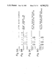
As shown in FIG. 5, around a drum 1 are provided a corona charger 2; laser light sources 3; developing machines 4, 6, 8, and 14, each with developers of cyan, yellow, magenta, and black; discharger 9; paper 10; and fur brush 11. The drum 1 comprises a conductive supporting body 1a and a photoconductive film 1b. The surface of the photoconductive film 1b is uniformly charged at a level of +800 V by the corona charger 2. Then electrostatic images are formed on the photoconductive film 1b by the laser light source 3.
Latent images corresponding to the development colors of for example, cyan 4a ( ○C ), yellow 6a ( ○Y ), and magenta 8a ( ○M ) are provided as shown in FIG. 6. The diameter of the dots of latent images which form various colors is 50 μm (micron), and the pitch of the latent images is 100 μm. Latent images corresponding to the three colors of cyan, yellow, and magenta are simultaneously formed at a latent image formation portion 30 by one scanning process of a laser beam.
In FIG. 7, a cyan developing machine comprises a magnetic roller 15 for agitation, by which a binary developer, consisting of carriers 20 of iron filings having a diameter of, for example, 100 to 200 μm, and of toners 21, i.e., fine particles colored with cyan, is agitated and charged by friction; a magnetic roller 16 for development which develops electrostatic latent images; a blade 17 which aligns the developer; a slit plate 18 for supplying the developer only to a position wherein latent images for cyan are formed; and a blade 19 for removing residual developer.
FIG. 8 shows the slit plate 18 in more detail. The slit plate 18, made of copper, has slits with a length of 20 mm, a width of 50 μm, a pitch distance of 300 μm, and a thickness of 200 μm. The slit plate 18 is aligned with the predetermined position of the cyan latent image so that only the cyan latent image can be developed with the cyan developing toners. Slit plates in the yellow and magenta developing machine have similar slits (as shown in FIG. 11). Use of such slit plates enables development of latent images for cyan, yellow and magenta without mixing and, therefore, improved color images, since the slit widths corresponding to the different colors do not overlap.
Returning to FIG. 5, in order to obtain a clear black color, a latent image is formed on the photoconductive film 1b by the laser light source 3 with a resolution limit of 10/mm. Then, the black latent image is developed by using high resistivity toners. These multicolor toner images are then transferred from the surface of the photoconductive film 1b to a paper 10 by a corona discharge 9. The residual toners on the drum 1 can be removed with a fur brush 11 by a well known process. The above multicolor printing process is continuously repeated.
FIGS. 9A to 9G illustrate changes of electric potential, in the above printing process. As shown in FIG. 9A, the surface of the drum 1 is first uniformly charged to +800 V. Then, the first latent image formation portions are formed at the corresponding cyan, yellow, and magenta positions. A latent image electric potential of +50 V is obtained corresponding to the above three colors, as shown in FIG. 9B. Then, only the cyan latent image, whose position is limited at the time of forming the latent images, is developed by the cyan developing machine 4 so that the cyan developing toner is adhered to the limited portion. The surface electric potential of the toner layer amounts to about 500 V, as shown in FIG. 9C. Similarly, yellow developing toners ( ○Y ) are adhered next to the cyan developing toners ( ○C ) by a yellow developing machine 6, as shown in FIG. 9D. Then magenta developing toners ( ○M ) are adhered next to the yellow developing toners ( ○Y ) by a magenta developing machine 8. The surface electric potential of the toner layers which develop various colors amounts to about 500 V, just as in the case of cyan. In this case, the bias voltage, Vb, for the development is maintained to 600 V to lower the back concentration.
Then, the second latent image formation portion corresponding to black is formed, and the electric potential of the latent image becomes 50 V, as shown in FIG. 9F. In the second latent image formation, magnetic toners having a mono-composition and high resistivity are used. The developing property of such high resistivity, mono-composition magnetic toners is such that the developing process occurs when the surface voltage V0 exceeds the threshold, 500 V, as shown in FIG. 10.
Thus, when the developing bias voltage of the magnetic brush developing machine is set to 800 V, black toners having a mono-composition are not adhered to the cyan, yellow, and magenta toners. Therefore, only black toner latent images are developed. As a result, the surface electric potential of the black toner becomes 300 V as shown in FIG. 9G.
Embodiments of the slit plates are illustrated in FIGS. 12 and 13.
The slit plates shown in FIGS. 12 and 13 are advantageous in that they allow positions corresponding to a latent image and to an area to be developed to be inspected.
In FIG. 12, a slit A for development has a slit width c of 50 μm, a pitch distance b of 300 μm, and a slit length d of 20 mm. Slit B for latent image formation has a rectangular shape with a width e of 50 μm and is a length l of 360 mm and formed above the slits A. A position marking slit C is provided at both sides of the slit plate. In FIG. 13, there are slits D for development and a slit E for latent image formation, corresponding to slit A and slit B. A position marking slit F, however, is not the same as slit C. Portions 14a are provided at the upper portion of slit E and directly above each slit D.
The process for synchronizing the latent image formation and development will now be explained below with reference to FIGS. 12 to 16. In FIG. 14, before a color latent image is formed, a laser scanning exposure is carried out. The time from when the laser scanning starts to when the laser scanning ends is measured and is equally divided to provide periodic color signal clocks. The color signal clocks, such as for cyan, are provided with a predetermined period at respective times. Then, the time from when the laser scanning starts to when the laser scanning ends is measured and is equally divided to correspond to another color signal clock.
Use of the slit according to the present invention provides an accurate one-to-one correspondence between the latent image formation and development for a plurality of colors, thus preventing mixing of colors. Furthermore, a color signal clock which reflects changes of temperature and aging can be obtained.
In the slit plate shown in FIG. 13, the dot patterns are formed at the latent image portion by a photomodulator only when the slit plate corresponds to the character and image pattern. At this time, the reflected laser light which hits the position inspecting mark can be read. This is input to a phase lock loop circuit as data. Then, the timing corresponding to the slit width is set on the basis of the color signal basic clock.
The embodiment of the slit shown in FIG. 13 can obtain more precise correspondence of the latent image and development thereof than the embodiment shown in FIG. 12.
As shown in FIG. 14, a beam emitted from a laser light source 21 is light modulated by photomodulator 22 and is deflected by a rotatable polygonal mirror 23. The deflected beam is collected at a predetermined position of a drum 25. In order to determine the correct position on the drum 1, the scanning beam is synchronized with such timing to enter an optical detecting device 2b provided at the scanning start position.
As shown in FIG. 15, the control system has a standard clock having the frequency of several times a printing dot clock. The beam entering the optical detecting device 2b is analog-to-digital converted, as a signal synchronized to the standard clock in a starting detecting circuit, to a starting signal. After the starting signal, a printing clock is provided by counting and dividing by n the standard clock. This printing clock corresponds to the printing position of, for example, cyan, yellow, and magenta in a multicolor printing process. By dividing the printing clock into three, a cyan (Y) clock, yellow (Y) clock, and magenta (M) clock are formed. To keep the clocks accurate, they are corrected by the printing clock according to the inputs to the AND circuit. By using such clocks, data concerning the colors is read to provide a series of data by an OR circuit. This data is latched by the printing clock and the optical modulator is operated by a NOW RETURN ZERO (NRZ) process.