BACKGROUND OF THE INVENTION
The invention relates to an exposure control device for a camera, and more particularly, to such device for automatically reading or sensing information in the form of a binary code defined on the surface of a film cartridge and representing film speed as such cartridge is loaded into a camera, thereby allowing a voltage corresponding to a particular value of film speed to be established for use in the decision of an exposure level.
An exposure control device which is capable of automatically reading information in the form of a binary code which may be defined by a conductive member printed on the surface of a film cartridge as such cartridge is loaded into a camera is already well known, as disclosed in Japanese Laid-Open Patent Application No. 51,736/1978, for example. However, a conventional exposure control device of this kind utilizes a complex electrical circuit, which resulted in an increased cost of a resulting camera.
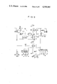
For a discussion of this aspect, a reference is made to the drawings. FIG. 1 is a circuit diagram of one form of exposure control device for a camera which is proposed in the prior art. In the exposure control device shown in FIG. 1, a terminal 1 is connected to a source of supply voltage +Vcc, and a light receiving element 2 and an integrating capacitor 3 are connected in series across the terminal 1 and the ground, with the junction between the element 2 and the capacitor 3 being connected to the ground through a switch 4 which remains closed, as shown, during the time a shutter remains closed. This junction is also connected to the non-inverting input terminal of a comparator 5 which is used as decision means to determine a proper amount of exposure. The comparator 5 also has an inverting input terminal which is connected to the junction between a pair of resistors 8, 9 connected in series across the terminal 1 and the ground and forming a voltage divider. The output terminal of the comparator 5 is connected to the terminal 1 through an electromagnet 6 which is effective to control the operation of a shutter. The element 2 may comprise a photoelectric transducer element such as may be formed by CdS (cadmium sulfide) element, for example, which exhibits a varying resistance with the brightness of an object being photographed.
The described device operates as follows: Initially, when a shutter is opened in response to a shutter release operation, the switch 4 is opened. Accordingly, a photocurrent flowing through the element 2 passes through the integrating capacitor 3 to charge it. Before the voltage Vc1 across the capacitor reaches a decision voltage VE which is determined by the voltage divider resistors 8, 9, the comparator 5 produces an output of a low level (which is hereafter referred to as "L" level) to maintain the electromagnet 6 energized, thus preventing the shutter from being closed. However, when the charged voltage Vc1 reaches the level of the decision voltage VE, the output from the comparator 5 changes to a high level (hereafter referred to as "H" level), thus deenergizing the electromagnet 6 to allow the shutter to be closed.
When the resistance of the element 2 is represented by RCdS, the resistance of the element 2 at a particular value of brightness by RCdSO, an incremental change from a reference brightness by ΔEV and the photoelectric conversion coefficient of the element 2 by γc, these parameters are related as indicated by the following equality:
R.sub.CdS =R.sub.CdSO 2.sup.-γ.sbsp.c.sup.ΔEV ( 1)
It will be apparent from the equation (1) that a change in the increment ΔEV causes a change in the resistance RCdS.
In the arrangement of FIG. 1, the voltage Vc1 across the capacitor 3 can be expressed in terms of the capacitance C1 of the capacitor 3 and the photocurrent iCdS of the element 2, as follows: ##EQU1## Thus, the exposure time t when the equality Vc1=VE applies is determined as follows: ##EQU2## The substitution of the equation (1) into the equation (3) yields: ##EQU3##
When films which exhibit different values of film speed are used, it is necessary that the level of the decision voltage which is used for the equality Vc1=VE must vary depending on such value of film speed. This may be achieved by changing the magnitude of the voltage Vc1 by employing a variable optical stop 7 disposed in front of the element 2 to change the amount of light received or by changing the level of the decision voltage VE by employing a variable ratio of division by the resistors 8, 9.
Considering a situation that the level of the decision voltage VE is changed by using a variable ratio formed by the resistors 8, 9 in accordance with a particular value of film speed, the decision voltage VE can be expressed as follows: ##EQU4## where R1 and R2 represent the resistance of the resistors 8, 9, respectively. Assuming that the resistances R1 and R2 are related such that R1 >>R2, we have ##EQU5## Accordingly, by changing the resistance R2 of the resistor 9, the decision voltage VE changes, thereby varying the exposure period t indicated by the equation (4). In order to accommodate for any selected value of film speed through a change in the resistance R2 of the resistor 9 rather than by the optical stop 7 disposed in front of the light receiving element 2, the resistance R2 must satisfy the following equation:
R.sub.2 =R.sub.02 2.sup.-γ.sbsp.c.sup.ΔSV ( 7)
where R02 represents a resistance of the resistor 9 for a standard film speed and can be suitably chosen in the design of the electrical circuit of the exposure control device, and ΔSV a change from the standard film speed. It will be seen that the equation (7) is similar in form to the equation (1). Thus, by changing the resistance R2 of the resistor 9 as an exponential function of the photoelectric conversion coefficient γc of the light receiving element 2, the decision voltage VE varies in accordance with the film speed, thus allowing an accommodation for any value of film speed.
FIG. 2 is a table of binary codes representing various values of film speed which are indicated in known form on a film cartridge. The binary code includes six bits, namely, bit A to bit F. Bits A to E are formed by a conductive area representing "1" or a non-conductive area representing "0" while the bit F comprises a common conductive area. In effect, film speed information is indicated by the five most significant bits A to E of the binary code, and only those bits which represent "1's" are connected to the common bit F. Accordingly, when a film cartridge carrying a binary code which represents a film speed is loaded into a camera, contacts SA to SE, which are disposed for reading the respective bits A to E in the binary code are turned on for a "1" bit and turned off for a "0" bit. By way of example, it will be seen from FIG. 2 that for a film speed of ISO 100, the read contacts SA to SE are operated such that SA is off, SB is on, SC is off, SD is on and SE is off.
Reference to FIG. 2 will indicate that the three most significant bits A, B and C of the binary code define a binary counter which is incremented by one for each 1 EV change in the film speed such as for ISO 25, 50, 100, . . . 1600, 3200, . . . Film speeds which are most frequently used are in a range from ISO 50 to 800. By choosing the resistance R2 of the resistor 9 for ISO 50 as a reference resistance R02, for example, the resistances for other values of film speed will be related as follows: ##EQU6## In other words, for those values of film speed in a range from ISO 50 to 800 which vary incrementally by 1 EV, a decision voltage VE corresponding to a particular value of the film speed will be obtained by choosing the resistance R2 of the resistor 9 shown in FIG. 1 in accordance with the equations (8). Accordingly, by providing a plurality of resistors having different resistances as indicated by the equations (8) in accordance with various ISO values of the film speed, and selecting one of these resistors for connection between the resistor 8 and the ground, a proper value of the decision voltage VE can be established. Such selection means may comprise a decoder as shown in FIG. 3, for example.
The decoder shown in FIG. 3 includes a terminal 11 to which the "1" or "0" signal of the bit A in the binary code is applied, a second terminal 12 to which the signal for the bit B is applied, and a third terminal 13 to which the signal for the bit C is applied. As shown, the terminal 11 is directly connected to each first input of AND gates 18, 20, 22, and is also connected through an inverter 14 to each first input of AND gates 17, 19, 21. The terminal 12 is directly connected to each second input of AND gates 19, 20 and is also connected through an inverter 15 to each second input of AND gates 17, 18, 21, 22. The terminal 13 is directly connected to each third input of AND gates 21, 22, and is also connected through an inverter 16 to each third input of AND gates 17 to 20.
When "1" or "0" signals of the bits A to C are applied to the terminals 11 to 13, one of the AND gates 17 to 22 develops an output of "H" level in accordance with the binary code, thus allowing one of the resistances indicated by the equations (8) to be selected.
FIG. 4 shows the electrical circuit of another exposure control device available in the prior art. The electrical circuit shown in FIG. 4 includes an electrical circuit portion comprising the light receiving element 2, integrating capacitor 3, comparator 5, electromagnet 6 and resistor 8 which are connected in the same manner as illustrated in FIG. 1. However, the resistor 9 is replaced by an automatic film speed presetting circuit including NPN transistors 31 to 47, PNP transistors 48 to 53, resistors 55 to 73 and read contacts SA to SE, all of which are connected between the non-inverting input of the comparator 5 and the ground, and a manual film speed presetting circuit including resistors 74 to 79 and a changeover switch 80.
When a film cartridge carrying a binary code which represents a film speed is loaded into a camera, it is assured that the read contact SD associated with the bit D or the read contact SE associated with the bit E will be turned on, as will be evident from FIG. 2. Accordingly, the transistors 48 and 32 are turned on, whereby the transistor 31 is turned off. This prevents the changeover switch 80 which is disposed to select one of the manual presetting resistors 74 to 79 from being connected to the ground, thus disabling the manual presetting circuit. The read contacts SA, SB and SC will be turned on or off in accordance with the bits A, B and C, whereby one of the transistors 33, 34, 37, 39, 43 and 45 will be turned on to connect one of the resistors 59, 62, 67, 68, 72 and 73 across the non-inverting input of the comparator 5 and the ground. It will be understood that these resistors 59 to 73 represent film speed values of ISO 25, 50, 100, 200, 400 and 800, and have resistances which are chosen in accordance with the equations (8). By way of example, if a film cartridge carries a binary code of "00010" representing ISO 25, only the read contact SD will be turned on. Where the read contacts SA, SB and SC associated with more significant bits are off, the transistor 33 is turned on to connect the resistor 59. By way of another example, if a film cartridge carries a binary code of "10010" representing ISO 50, the read contacts SA and SD will be turned on. When the contact SA is turned on, the transistor 49 is turned on, whereby the transistors 34 and 35 will be turned on while the transistor 33 will be turned off, thus connecting the resistor 62. By way of a further example, if the binary code is "11010" representing ISO 200, the read contacts SA, SB and SD will be turned on. When both the contacts SA and SB are on, the transistors 50 and 51 are turned on, whereby the transistor 36 is turned on, the transistors 37, 38 will be turned off, and the transistors 39 to 41 will be turned on. Accordingly, the base-emitter path of the transistor 33 as well as the base-emitter path of the transistor 34 will be short-circuited, turning the transistors 33, 34 off. Hence, only the resistor 68 will be connected in this instance. In a similar manner, the resistor 72 will be connected for ISO 400 and the resistor 73 will be connected for ISO 800. Finally, the resistor 67 will be connected for ISO 100.
When a film cartridge carrying no binary code is loaded into a camera, all of the read contacts SA to SD remain off, and hence the transistors 48, 32 are off to allow the transistor 31 to be turned on, whereby one of the manual presetting resistors 74 to 79 will be selected by the changeover switch 80 to be connected to the ground. The resistors 74 to 79 correspond to ISO 25 to 800, respectively, and have resistances as indicated by the equations (8). In this manner, a film speed from ISO 25 to 800 can be manually selected.
It will be understood from the above description that the device shown in FIG. 4 allows a decision voltage to be established by reading a binary code indicated on the surface of a film cartridge. However, the circuit diagram of FIG. 4 indicates that the device utilizes an increased number of electronic parts such as transistors, disadvantageously requiring a very complex circuit arrangement.
SUMMARY OF THE INVENTION
In view of the foregoing, it is an object of the invention to provide an exposure control device for camera which uses a simple circuit arrangement.
In accordance with the invention, a plurality of automatic film speed presetting resistors are provided and connected to corresponding read contacts. These resistors have resistances which are chosen to be in a given ratio with respect to a particular resistance which is associated with a typical value of film speed. By using a photometric circuit having a photoelectric conversion coefficient which is suitably chosen, a greatly simplified arrangement may be used to read a binary code indicated on the surface of a film cartridge to represent different values of film speed which vary by at least 1 EV interval in order to establish a reference or decision voltage automatically with a reduced exposure error for use in the decision of an exposure level. This arrangement can be advantageously utilized in a compact camera, in particular.
BRIEF DESCRIPTION OF THE DRAWINGS
FIG. 1 is a circuit diagram of one form of conventional exposure control device;
FIG. 2 is a table indicating various binary codes indicated on a film cartridge to represent various values of film speed;
FIG. 3 is a circuit diagram of one form of decoder which may be used to read the binary code;
FIG. 4 is a circuit diagram of another electrical circuit of a conventional exposure control device;
FIG. 5 is a circuit diagram of an exposure control device according to one embodiment of the invention;
FIG. 6 graphically illustrates deviations ΔEV from proper exposure values corresponding to the photoelectric conversion coefficient γc at various values of film speed when the automatic presetting resistors shown in the device of FIG. 5 have resistances which are chosen in the ratio of 1:α:α3 ;
FIG. 7 graphically shows the deviations ΔEV, in a manner similar to that shown in FIG. 6, when the automatic presetting resistors used in the device of FIG. 5 have resistances which are chosen in the ratio of α4 /(1-α):α:α3 ;
FIG. 8 is a circuit diagram of an exposure control device according to another embodiment of the invention; and
FIG. 9 is a circuit diagram of an exposure control device according to a further embodiment of the invention.
DETAILED DESCRIPTION OF PREFERRED EMBODIMENTS
FIG. 5 is a circuit diagram of an exposure control device for camera which is constructed in accordance with one embodiment of the invention. As shown, the device includes a terminal 101 to which a supply voltage +Vcc is applied. A series combination of a light receiving element 102 and an integrating capacitor 103 is connected between the terminal 101 and the ground, and the junction therebetween is connected to the ground through a switch 104 which remains closed as long as a shutter remains closed. The junction is also connected to the non-inverting input of a comparator 105 which is used to determine an exposure level. The comparator 105 has its inverting input connected to the terminal 101 through a voltage divider resistor 108 and its output terminal connected to the terminal 101 through an electromagnet 106 which controls the operation of a shutter.
It will be noted that the inverting input of the comparator 105 is connected to one end of each of automatic presetting resistors 109 to 111, the other end of which is connected to the ground through read contacts SA, SB and SC, respectively. The inverting input of the comparator 105 is also connected to one end of each of a plurality of manual presetting resistors 112 to 116, the other end of which is connected to fixed contacts a to e, respectively, of a changeover switch 117. The changeover switch 117 has a movable contact which is connected to the collector of an NPN transistor 118. The base of the transistor 118 is connected to the collector of an NPN transistor 119 and is also connected to the terminal 101 through a resistor 120. The transistors 118 and 119 have their emitters connected to the ground, and the base of the transistor 119 is connected through a resistor 121 to the collector of a PNP transistor 122. The transistor 122 has its emitter connected to the terminal 101 and its base connected through a resistor 123 to one terminal of each of read contacts SD and SE which are connected in parallel and have their other end connected to the ground.
Among the resistors described above, the manual presetting resistors 112 to 116 correspond to ISO 50, 100, 200, 400 and 800, and have resistances which are chosen in accordance with the equations (8). The automatic presetting resistors 109 to 111 correspond to ISO 50, 100 and 400, and have resistances RA to RC which are chosen such that RA =R02, RB =αR02 and RC =α3 R02. As mentioned previously, R02 represents a resistance corresponding to a standard film speed and α is represented as α=2-γ c where γc represents the photoelectric conversion coefficient of the element 102.
In operation, when a film cartridge carrying no binary code is loaded into a camera, all of the read contacts SA to SE remain off. Accordingly, the transistors 122, 119 remain off while the transistor 118 is turned on. Thus, the movable contact of the changeover switch 117 is connected to the ground, allowing one of the manual presetting resistors 112 to 116 which is selected by the switch 117 to be connected between the inverting input of the comparator 105 and the ground. Thus, a decision voltage VE which is obtained by the substitution of one of the equations (8) into the equation (6) is applied to the inverting input of the comparator 105. Subsequently when the switch 104 opens in response to a shutter release operation, the photocurrent from the element 102 begins to charge the integrating capacitor 103 until the voltage Vc1 becomes equal to VE, whereupon the comparator 105 produces an output of "H" level, deenergizing the electromagnet 106 to allow the shutter to be closed.
When a film cartridge carrying a binary code is loaded into a camera, the read contacts SA to SE are selectively turned on or off in accordance with the binary code. Since it is assured that either one of the read contacts SD and SE which are associated with the two least significant digits of the binary code is turned on, the transistor 122 is turned on, whereby the transistor 119 is turned on. This turns the transistor 118 off, disconnecting the movable contact of the changeover switch 117 from the ground to disable the manual presetting circuit.
Considering the read contacts SA to SC associated with the three most significant digits of the binary code, it will be seen from an inspection of FIG. 2 that the contact SA is on for ISO 50, the contact SB is on for ISO 100, the contacts SA and SB are on for ISO 200, the contact SC is on for ISO 400 and the contacts SA and SC are on for ISO 800. Accordingly, when the film speed changes at an interval of 1 EV in a range from ISO 50 to 800, the resistance R2 between the inverting input of the comparator 105 and the ground changes as follows: ##EQU7##
A comparison of the equations (9) with the equations (8) indicates that a coincidence is established therebetween for film speed values ISO 50, 100 and 400, meaning that the resulting decision voltage VE applied to the inverting input of the comparator 105 is theoretically correct. However, for ISO 200 and 800, the resistances indicated by the equations (9) show a composite resistance which is different from that indicated by the equations (8), and hence the resulting decision voltage VE will be different from a theoretical value corresponding to the film speed.
Representing the theoretical value of the resistance by RT, the actual resistance by RE and the resulting deviation ΔEV, we have
R.sub.E =R.sub.T 2.sup.γ.sbsp.c.sup.ΔEV (10)
For ISO 200, we have ##EQU8## The substitution of the equations (11) into the equation (10) yields: ##EQU9## Accordingly, representing the deviation for ISO 200 by ΔEV200, we have ##EQU10##
Smilarly, for ISO 800, we have ##EQU11## Combining the equations (13) and (10), the deviation ΔEV800 for ISO 800 is given as follows: ##EQU12## Rewriting α=2-γc in the equations (12) and (14) yields: ##EQU13## The deviation ΔEV200 and ΔEV800 are related to α and γc (photoelectric conversion coefficient) as indicated in Table 1 below:
              TABLE 1
______________________________________
          ΔEV
α
       γ.sub.c
                ISO 200  ISO 800
                                ISO 1600
                                       ISO 3200
______________________________________
0      ∞  1.00     1.00   3.00   3.00
                (EV)     (EV)   (EV)   (EV)
0.1    3.32     0.96     1.00   2.96   3.00
0.2    2.32     0.89     1.00   2.89   2.97
0.3    1.74     0.78     0.98   2.78   2.91
0.4    1.32     0.63     0.93   2.63   2.78
0.5    1.00     0.42     0.83   2.42   2.54
0.6    0.74     0.08     0.62   2.08   2.11
0.618  0.694    0.00     0.56   2.00   2.00
0.676  0.565    -0.32    0.32   1.68   1.55
0.7    0.514    -0.49    0.17   1.51   1.30
0.724  0.466    -0.69    0.00   1.31   1.00
0.755  0.405    -1.00    -0.27  1.00   0.54
0.8    0.32     -1.63    -0.85  0.37   -0.43
0.809  0.306    -1.80    -1.00  0.20   -0.69
0.9    0.15     -5.09    -4.20  -3.09  -5.84
1.0    0        -∞ -∞
                                -∞
                                       -∞
______________________________________
The relationship between the deviations ΔEV200 and ΔEV800 given by the equations (15) and (16) and the photoelectric conversion coefficient γc is graphically illustrated in FIG. 6. It will be apparent from the Table 1 and FIG. 6 that the magnitude of the deviation ΔEV from a proper exposure value can be kept within a permissible range for film speeds of ISO 200 and 800, by a suitable choice of the photoelectric conversion coefficient γc.
By way of example, when a choice is made that γc =0.565, it follows that ΔEV200 =-0.32 EV and ΔEV800 =+0.32 EV. In other words, the absolute value of both deviations can be made equal to each other. It can be shown that for 0.466≦γc ≦0.694, we have -0.69 EV≦ΔEV200 ≦0 and 0≦ΔEV800 ≦0.56 EV, and this means that the magnitude of the deviations for ISO 200 and 800 can be kept within 2/3 EV. If the deviation ΔEV for ISO 200 and 800 is allowed in a range given by the inequality -1 EV≦ΔEV≦1 EV, the photoelectric conversion coefficient γc can be freely chosen in a range 0.405 ≦γc ≦∞.
Thus in the exposure control device shown in FIG. 5, the resistances RA to RC of the automatic presetting resistors 109 to 111 are chosen in the ratio of 1:2-γc :2-3γc and a suitable value for the photoelectric conversion coefficient γc is chosen, thereby allowing the decision voltage VE to be kept within a desired range of exposure errors.
In the above description, an accommodation for film speeds from ISO 50 to 800 has been assumed, but an accommodation for film speeds of ISO 1600 and 3200 is also possible. The theoretical value RT of the automatic presetting resistors for ISO 1600 and 3200 are given as follows: ##EQU14## On the other hand, the actual values RE are given as follows: ##EQU15## Combining the equations (10), (17) and (18), the deviations ΔEV1600 and ΔEV3200 for ISO 1600 and 3200 can be given as follows: ##EQU16## The relationship between the deviations ΔEV1600 and ΔEV3200 on one hand and the α and γc on the other hand is indicated in the Table 1 given above, and these deviations are related to the photoelectric conversion coefficient γc as graphically shown in FIG. 6. Accordingly, it will be seen from the Table 1 and FIG. 6 that the latitude for the choice of γc will be substantially limited if it is desired to keep the deviation ΔEV for film speeds of ISO 200, 800, 1600 and 3200 within +1 EV. For example, when a choice is made that γc =0.405, it follows that ΔEV200 =-1.00 EV, ΔEV800 =0.27 EV, ΔEV1600 =1.00 EV and ΔEV3200 =0.54 EV, barely satisfying the desired limitation. Hence, if an exposure error within ±1 EV is permitted, a light receiving element having γc =0.405 may be used to achieve an automatic accommodation for film speeds in a range from ISO 50 to 3200.
To achieve a theoretical resistance for ISO 50, 100, 400, the resistances of the automatic presetting resistors 109 to 111 used in the electrical circuit of FIG. 5 have been chosen in the ratio of 1:α:α3, or RA =R02, RB =αR02 and RC =α3 R02. However, a theoretical resistance for other ISO values may be chosen. For example, if it is desired to establish theoretical resistances for ISO 100, 400 and 800, it is seen from the equations (8) that ##EQU17## In this instance, we have ##EQU18## Accordingly, theoretical resistances for film speeds of ISO 100, 400 and 800 can be established by choosing the resistances RA to RC in the ratio of RA :RB :RC =α4 /(1-α):α:α3, thus reducing the deviation αEV to zero for these film speeds. In this instance, the deviation for other film speeds, namely, αEV50, αEV200, αEV1600 and αEV3200 for ISO 50, 200, 1600 and 3200 are given as follows: ##EQU19##
The deviation αEV indicated by the equations (22) are graphically related to the photoelectric conversion coefficient γc as shown in FIG. 7. It will be evident from the illustration of FIG. 7 that a choice of the photoelectric conversion coefficient γc in a range from 0.38 to 0.56 permits the deviations for ISO 50, 200, 1600 and 3200 to be kept within ±1 EV. This represents a greater latitude for the choice of γc in contrast to the choice of the ratio 1:α:α3 where the deviation ΔEV can barely be kept within ±1 EV only when a choice is made that γc =0.405. A particular value of γc can be chosen to minimize the resulting exposure error.
FIG. 8 is a circuit diagram of an exposure control device according to another embodiment of the invention which permits film speed information from ISO 25 to 800 which can be read at an interval of 1 EV. The electrical circuit shown in FIG. 8 is generally similar to that shown in FIG. 5 except that automatic presetting resistors 131 to 134 have their one end connected to the inverting input of the comparator 105, to which the voltage divider resistor 108 is connected. The other end of each of the resistors 132 to 134 is connected to the ground through the read contacts SA to SC, respectively, while the other end of the resistor 131 is connected to the collector of an NPN transistor 135. The automatic presetting resistors 131 to 134 have resistances R25, RA, RB and RC which are chosen as will be described later. The transistor 135 has its emitter connected to the ground and its base connected through a resistor 136 to the collector of the transistor 122. It is to be understood that the manual presetting resistors 137 to 142 are chosen so as to correspond to those values of film speed within a range from ISO 25 to 800 which vary at an interval of 1 EV. These resistors have their one end connected to the inverting input of the comparator 105 and their other end connected to each fixed contact a to f of a changeover switch 117A.
In the device shown in FIG. 8, when a film cartridge carrying no binary code is loaded into a camera, all of the read contacts SA to SE remain off, and hence the transistors 122, 119 and 135 are off while the transistor 118 is turned on, thus allowing one of the resistors 137 to 142 which is selected by the changeover switch 117A to be connected between the inverting input of the comparator 105 and the ground. Accordingly, a decision voltage VE as determined in accordance with the equations (6) and (8) is applied to the inverting input of the comparator 105. It is to be noted that the resistor 137 for ISO 25 has a resistance of α-1 R02.
When a film cartridge carrying a binary code is loaded into a camera, the read contacts SA to SE are selectively turned on and off in accordance with the binary code. Since at least one of the contacts SD and SE is turned on as mentioned previously, the transistors 122 and 119 are turned on while the transistor 118 is turned off to disable the manual presetting circuit. As the transistor 122 is turned on, the transistor 135 is turned on, whereby the resistor 131 is connected between the inverting input of the comparator 105 and the ground. Thus, the resistor 131 is connected to the comparator 105 whenever a film cartridge carrying a binary code is loaded into a camera. When the film speed indicated on the surface of the film cartridge is ISO 25, all of the read contacts SA to SC are off, and hence only the resistor 131 will be connected to the comparator 105.
As will be appreciated, the resistance R2 for each film speed of ISO 50, 100, 400 and 800 should theoretically be as follows: ##EQU20## Solving the equations (23) for the resistances R25, RA, RB and RC, we have: ##EQU21## Thus, when the resistances R25, RA, RB and RC of the automatic presetting resistors 131 to 134 are chosen in accordance with the equations (24), theoretical resistances are established for film speeds of ISO 50, 100, 400 and 800. Accordingly, the deviation ΔEV is equal to zero in this instance.
In this instance, the resistance for film speed of ISO 25 and 200 will deviate from theoretical values. The theoretical resistance of the automatic presetting resistor for ISO 25 and 100 is given as follows: ##EQU22## On the other hand, the actual value will be as follows: ##EQU23## Combining the equations (25) and (26) with the equation (10), the deviations ΔEV25 and ΔEV200 for ISO 25 and 200 are obtained as follows: ##EQU24## It will be seen that by choosing a value for the photoelectric conversion coefficient γc which enables the deviations ΔEV25 and ΔEV200 to be kept within a permissible range of exposure errors, an automatic accommodation for a range of film speeds from ISO 25 to 800 is achieved at an interval of 1 EV.
It is to be understood that an automatic accommodation for film speeds of ISO 1600 and 3200 can also be achieved in the device described above. Specifically, when the resistances R25, RA, RB and RC of the resistors 131 to 134 are chosen in accordance with the equations (24), the theoretical value RT and the actual value RE for ISO 1600 and 3200 will be as follows: ##EQU25## The resulting deviations ΔEV1600 and ΔEV3200 are given as follows: ##EQU26## It will thus be seen that by choosing a value of the photoelectric conversion coefficient γc so that the deviations ΔEV25, ΔEV200, ΔEV1600 and ΔEV3200 can be kept within a permissible range of exposure errors, the automatic accommodation for film speeds in a range from ISO 25 to 3200 can be achieved at an interval of 1 EV.
FIG. 9 is a circuit diagram of an exposure control device according to a further embodiment of the invention. In this embodiment, a light receiving element 152 comprises a silicon photodiode (SPD) which is used as a photoelectric transducer element. It will be noted that the electrical circuit shown in FIG. 9 is substantially similar to the electrical circuit shown in FIG. 5 except for a circuit portion associated with the light receiving element 102. It will be seen that the element 102 is replaced in this embodiment by a photometric circuit 151 which includes light receiving element 152, logarithmic compression diode 153, operational amplifiers 154, 155, resistors 156, 157 and transistors 159 to 161. Specifically, in the photometric circuit 151, the anode of the element 152 or silicon photodiode is connected to the non-inverting input of the operational amplifier 154 which is connected to the ground while its cathode is connected to the inverting input of the amplifier 154 and to the cathode of the logarithmic compression diode 153. The output terminal of the amplifier 154 is connected to the anode of the diode 153 and also connected to the ground through a series combination of voltage divider resistors 156, 157. The resistor 156 is formed by a semi-fixed resistor so that its resistance can be varied. The junction between the resistors 156 and 157 is connected to the non-inverting input of the amplifier 155, which has its inverting input connected to the output thereof, thereby forming an impedance converting buffer amplifier. The output of the amplifier 155 is connected to the base of an NPN transistor 159, which has its emitter connected to the ground and its collector connected to the bases of PNP transistors 160, 161 and to the collector of the transistor 160. The transistors 160 and 161 form a current mirror circuit, and their emitters are connected in common to the terminal 101, to which the supply voltage is applied. The collector of the transistor 161 is connected to the non-inverting input of the comparator 105, to which both the integrating capacitor 103 and the switch 104 are connected.
In operation, when a photocurrent I1 flows through the element 152 in accordance with the amount of incident light, there is developed a voltage V1 at the output of the amplifier 154 which represents a logarithmic compression of the photocurrent I1. Specifically, a relationship is established as indicated below: ##EQU27## where Is represents a saturation current, k Boltzmann's constant (8.62×10⁻⁵ ev/°K.), q the charge of an electron (1.6×10⁻¹⁴ C.) and T the absolute temperature (°K.). At room temperature, the term "-1" appearing in the equation (31) can be omitted, and hence this equation can be solved for V1 as follows: ##EQU28## Representing the photocurrent which flows at a reference level of brightness by Is which is equal to the saturation current, a difference in the brightness level from a reference level by ΔEV.sub.(EV) and the photoelectric conversion coefficient of the silicon photodiode by γSPD, we have:
I.sub.1 =Is·2.sup.Δ.sbsp.SPD.sup.·ΔEV(33)
The substitution of the equation (33) into the equation (32) yields: ##EQU29## Since the photoelectric conversion coefficient γSPD of a silicon photodiode is usually equal to 1, the equation (34) can be rewritten as follows: ##EQU30## This means that the output voltage V1 from the amplifier 154 depends on the difference in the brightness level ΔEV from the reference level. The voltage V1 is divided by a voltage divider formed by the resistors 156 and 157, and the divided voltage is applied to the amplifier 155. Representing the resistances of the resistors 156, 157 by R3 and R4, respectively, the output voltage V2 from the amplifier 155 is expressed as follows: ##EQU31##
Using an equality R4/(R3+R4)=γc, the equation (36) can be rewritten as follows: ##EQU32## The current I2 which passes across the base and the emitter of the transistor 159 is given as follows: ##EQU33## From the equation (38), we have: ##EQU34## Combining the equations (37) and (39), we have:
I.sub.2 =Is 2.sup.γ.sbsp.c.sup.·ΔEV (40)
It will be noted that the equation (40) is similar in form to the equation (33). In other words, the magnitude of the current I2 is determined by the value of γc which is in turn determined by the ratio of the resistances R3 and R4 of the resistors 156 and 157. Since the transistors 160, 161 form a current mirror circuit, a charging current I3 to the integrating capacitor 103 has a magnitude which is proportional to the current I2, or ##EQU35## where hfe represents the current amplification factor of the transistor 159. It is seen that the charging current I3 to the integrating capacitor 103 can be varied by changing the value of γc, which can be considered as the photoelectric conversion coefficient of the photometric circuit 151.
It will therefore be seen that an automatic accommodation for film speeds in a range from ISO 50 to 800 can be achieved at an interval of 1 EV when a silicon photodiode having the photoelectric conversion coefficient γSPD =1 is used in an exposure control device, by choosing the resistances RA to RC of the automatic presetting resistors 109 to 111 for film speeds of ISO 50, 100 and 400 in the ratio mentioned above (1:α:α3), and adjusting the semi-fixed resistor 156 in the photometric circuit 151 to establish a suitable value for the photoelectric conversion coefficient γc such that the deviations ΔEV in the amount of exposure form a theoretical value can be kept within a permissible range for film speeds of ISO 200 and 800 for which theoretical resistances cannot be employed.