BACKGROUND OF THE INVENTION
The present invention generally relates to digital video signal transmitting apparatuses, and more particularly to a transmitting apparatus which transmits a digital video signal made up of picture element data corresponding to one field, by dividing the digital video signal into a plurality of picture element groups each corresponding to less than one field, to store the data of the digital video signal into a memory, and obtains a reproduced video signal by reading the same stored data from the memory a plurality of times.
When the signal-to-noise level at the time of the reproduction is over a predetermined value, a digital signal can be restored back to the original digital signal. Hence, in order to carry out recording and reproduction of a high quality, a digital video signal is recorded on and reproduced from a recording medium such as a magnetic tape and a disc. The digital video signal is obtained by subjecting an analog video signal to a digital pulse modulation such as a pulse code modulation, for example. In this case, when transmitting a digital video signal related to a still picture or related to a so-called partially moving picture in which only a part of the picture contains a movement, it is desirable to transmit as much video information as possible under the limitation of the recording capacity of the recording medium. Thus, a digital video signal corresponding to one field which is less than one frame which is originally to be reproduced was transmitted, or a so-called differential transmitting method was employed in the case of the partially moving picture, for example. According to the differential transmitting method, the frame correlation of the video information was noted, and a differential data between the picture element data of one frame and the picture element data of a subsequent frame was transmitted when the subsequent frame included picture element data different from the picture element data in the one frame.
When transmitting the digital video signal corresponding to one field, only the data related to the picture elements in one of first and second fields (odd and even fields) were transmitted among the picture elements which are arranged in a matrix form to make up one picture. For this reason, the vertical resolution of the reproduced picture obtained in this case, inevitably became poorer than the vertical resolution of the reproduced picture obtained when all of the picture element data corresponding to one frame was transmitted. Further, the folding noise increased, and when the picture contained an oblique line, for example, the oblique line was reproduced as a stepped line. Moreover, when the picture contained horizontal lines which differed in their thicknesses and positions, these differences were over-emphasized in the reproduced picture.
In addition, in a case where the differential transmitting method was employed and a large portion of the picture changed to a different picture, the different picture could not be displayed in the large portion of the picture until all of the digital video signals (picture element data) related to the different picture were stored into the memory within the reproducing apparatus. As a result, it took a long time to change the display in the large portion of the picture to the different picture.
SUMMARY OF THE INVENTION
Accordingly, it is a general object of the present invention to provide a novel and useful digital video signal transmitting apparatus in which the problems described heretofore have been eliminated.
Another and more specific object of the present invention is to provide a digital video signal transmitting apparatus in which, when writing a picture element data of an input digital video signal into a memory, the picture element data is compared with a picture element data which is related to the same picture element position but was obtained previously, and one or a plurality of previously written picture element data are replaced by the input picture element data or one or a plurality of data obtained by interpolating the input picture element data, according to a value which is obtained as a result of the comparison. A reproduced analog video signal is formed from the picture element data which are read out from the memory. According to the apparatus of the present invention, it is possible to obtain a reproduced picture within a short time which is in the range of a duration of one field, and the deterioration of the picture can be kept to a minimum by use of the frame correlation, compared to a case where a digital video signal corresponding to one field is transmitted and to a case where the differential transmitting method is employed when the displayed picture is to be changed. In addition, when transmitting a partially moving picture, a number of picture element data corresponding to the speed of the movement in the picture can be replaced. Hence, it is possible to display a picture which contains a quick movement, and further, it is possible to obtain an essentially perfectly still picture when displaying a still picture.
Still another object of the present invention is to provide a digital video signal transmitting apparatus which transmits a video signal having a wide band in a single channel of transmission path having a narrow band. According to the apparatus of the present invention, it is possible to reduce the sampling frequency to 1/4 compared to the sampling frequency in the conventional apparatus, by dividing all of the picture element data of a video signal amounting to one field into four groups and successively transmitting each of the divided picture element data groups for every field. As a result, the band of the digital video signal which is transmitted, can be compressed.
A further object of the present invention is to provide a digital video signal transmitting apparatus which produces a reproduced analog video signal so that, between reproducing durations of first and second fields (odd and even fields), the picture element data of the first and second fields are alternately arranged and displayed in one scanning line, and the combination of the picture element data of the first and second fields displayed in the one scanning line is different between the reproducing durations of the first and second fields. According to the apparatus of the present invention, it is possible to visually reduce the noise due to the folding distortion, and it is also possible to reduce the apparent vertical resolution of the reproduced picture.
Other objects and further features of the present invention will be apparent from the following detailed description when read in conjunction with the accompanying drawings.
BRIEF DESCRIPTION OF THE DRAWINGS
FIG. 1 is a systematic block diagram showing an embodiment of a recording system for a digital video signal which is to be transmitted by a digital video signal transmitting apparatus according to the present invention;
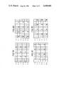
FIGS. 2A, 2B, 2C, and 2D show embodiments of positions of picture element data of a digital video signal within a picture, which digital video signal is to be transmitted by the digital video signal transmitting apparatus according to the present invention;
FIG. 3 shows an embodiment of positions of picture element data of a digital video signal within a picture, which digital video signal is to be transmitted by the digital video signal transmitting apparatus according to the present invention;
FIG. 4 is a systematic block diagram showing an embodiment of a digital video signal transmitting apparatus according to the present invention;
FIG. 5 is a systematic block diagram showing an embodiment of an essential part of the block system shown in FIG. 4;
FIGS. 6(A) through 6(F) show signal waveforms for explaining the operation of the block system shown in FIG. 5;
FIGS. 7(A) through 7(D) show signal waveforms for explaining the operation of the block system shown in FIG. 5;
FIGS. 8A, 8B, 8C, and 8D diagrammatically show the relationships between memory element groups in the block system shown in FIG. 5 and write-in control pulses;
FIGS. 9A and 9B show positions of picture element data in the picture in reproducing durations of first and second fields;
FIGS. 10A, 10B, and 10C show examples of picture element parts in which the same picture element data in the first column from the left of the picture are displayed;
FIGS. 11A, 11B, and 11C show examples of picture element parts in which the same picture element data in the second column from the left of the picture are displayed;
FIGS. 12A, 12B, and 12C show examples of picture element parts in which the same picture element data in the third column from the left of the picture are displayed;
FIGS. 13A, 13B, and 13C show examples of picture element parts in which the same picture element data in the fourth column from the left of the picture are displayed; and
FIGS. 14A, 14B, 14C, and 14D show other embodiments of positions of picture element data of a digital video signal within a picture, which digital video signal is to be transmitted by the digital video signal transmitting apparatus according to the present invention.
DETAILED DESCRIPTION
In FIG.1, primary color signals R, G, and B of red, green, and blue which are obtained by picking up an image by a color television camera of a system which employs 625 scanning lines, for example, are applied to respective input terminals 11, 12, and 13. These primary color signals R, G, and B are supplied to a matrix circuit 14 which forms a luminance signal Y, and color difference signals (R-Y) and (B-Y) from these primary color signals R, G, and B. The luminance signal Y and the color difference signals (R-Y) and (B-Y) are respectively supplied to an analog-to-digital (AD) converter 15. The AD converter 15 samples and then quantizes the analog signals from the matrix circuit 14, and forms a digital signal (picture element data) having a quantization number of 8 bits for one picture element (sampling point), for example. The picture element data from the AD converter 15, are supplied to a memory 16. The digital luminance signal and the two kinds of digital color difference signals are respectively written into the memory 16 in response to a write-in pulse from a read/write controller 17. Among picture element data which make up one picture and are obtained by subjecting the analog video signal to a digital pulse modulation, picture element data which are arranged in a checkered pattern in the picture and correspond to one field, are serially read out from the memory 16 under the control of the read/write controller 17.
Description will now be given with respect to the read-out operation of the memory 16 in the digital video signal transmitting apparatus according to the present invention. For convenience' sake, it will be assumed that 16 luminance picture element data are arranged in the horizontal direction and 6 luminance picture element data are arranged in the vertical direction in one picture (one frame), for example. In this case, as shown in FIG. 2A, picture element data which are arranged at positions [1], [5], [9], and [13] in a first scanning line I-1 of the first field (odd field), picture element data which are arranged at positions [17], [21], [25], and [29] in a second scanning line I-2 of the first field, and picture element data which are arranged at the positions [33], [37], [41], and [45] in a third scanning line I-3 of the first field, are successively read out from the memory 16 in a duration of one field. Thereafter, predetermined picture element data which are arranged in the first, second, and third scanning lines II-1, II-2, and II-3 of the second field (even field), are successively read out from the memory 16 in a duration of one field. As shown in FIG. 2C, predetermined picture element data which are arranged in first, second, and third scanning lines I-1, I-2, and I-3 of the first field, are then successively read out from the memory 16 in a duration of one field. Further, as shown in FIG. 2D, predetermined picture element data which are arranged in the first, second, and third scanning lines II-1, II-2, and II-3 of the second field, are finally and successively read out from the memory 16 in a duration of one field. As shown in FIGS. 2A through 2D, the predetermined picture element data which are arranged in one scanning line and are read out from the memory 16, are mutually separated by three picture element data positions in the horizontal direction of the picture. As a result, among all of the luminance picture element data which make up one picture, the luminance picture element data which correspond to one field and are arranged in a checkered pattern at positions indicated by hatchings in FIG. 3, are read out from the memory 16 in a duration of four fields.
FIG. 2A shows the picture element data in the first, fifth, ninth, and thirteenth columns from the left of the picture, among the picture element data corresponding to the first field. FIG. 2C shows the picture element data in the third, seventh, eleventh, and fifteenth columns from the left of the picture, among the picture element data corresponding to the first field. FIG. 2B shows the picture element data in the second, sixth, tenth, and fourteenth columns from the left of the picture, among the picture element data corresponding to the second field. Further, FIG. 2D shows the picture element data in the fourth, eighth, twelfth, and sixteenth columns from the left of the picture, among the picture element data corresponding to the second field.
Among all of the picture element data corresponding to one frame, the memory 16 divides the picture element data indicated by the hatchings in FIG. 3 which amounts to one field, into four groups as shown in FIGS. 2A through 2D. Each of the divided picture element data groups are successively read out from the memory 16 for every one field period. In other words, the picture element data amounting to one field are decimated (or cut) to 1/4 when read out from the memory 16 for one field period. Accordingly, the sampling frequency of the digital video signal in which the picture element data read out from the memory 16 are time-sequentially multiplexed, becomes 1/4 the sampling frequency fs in the AD converter 15, and the upper limit frequency of the transmission band of the digital video signal becomes equal to fs /8. Hence, the digital video signal from the memory 16 is transmitted in an extremely narrow band compared to the transmission band of the conventional apparatus.
On the other hand, picture element data of the two kinds of color difference signals (R-Y) and (B-Y) which are arranged at the positions indicated by the hatchings in FIG. 3, are also read out from the memory 16. For example, a digital video signal read out from the memory 16 has a signal format in which data are transmitted time-sequentially in terms of units, where one unit is made up of four luminance picture element data and one picture element data of each of the two kinds of color difference signals (R-Y) and (B-Y). The digital video signal read out from the memory 16, is supplied to a signal processing circuit 18 wherein the digital video signal is time-sequentially multiplexed with a digital audio signal or a control signal for random access from an input terminal 19. An output digital signal of the signal processing circuit 18, is supplied to a modulating circuit 20. The modulating circuit 20 modulates the incoming digital signal based on a predetermined modulating system, such as a frequency modulation system, which is suited for recording and reproduction. A modulated signal from the modulating circuit 20, is supplied to a recording device 21.
For example, the recording device 21 obtains a modulated laser beam by modulating a laser beam by the modulated signal from the modulating circuit 20, and a photosensitive agent on an original recording disc is intermittently exposed to the modulated laser beam. The original recording disc is then subjected to known developing and disc manufacturing processes, and the recording device 21 produces a disc 22. The digital video signal and the like are recorded on a spiral track on the disc 22.
The present invention relates to an apparatus for transmitting the digital video signal from the disc 22 and the like, that is, for reproducing the digital video signal from the disc 22 and the like, for example. In FIG. 4, the disc 22 is recorded with a digital video signal which has been frequency modulated, for example. Among picture element data corresponding to one frame of an arbitrary picture, picture element data which correspond to one field and in which picture element data of the first and second fields coexist in a duration of four fields due to the processing in the recording system shown in FIG. 1, are time-sequentially multiplexed in the digital video signal recorded on the disc 22. In other words, the video signal corresponding to one field, is transmitted with 1/4 the original number of picture element data. In order to reduce the memory capacity which is required to store the digital video signal, the digital video signal does not include signals such as a horizontal synchronizing signal, a vertical synchronizing signal, and a color burst signal.
The disc 22 is rotated by a motor 26, and the recorded signal is reproduced from the disc 22 by a pickup device 27. The pickup device 27 may be of a type which picks up and reproduces the recorded signal from the disc 22 according to the variation in the electrostatic capacitance between the disc 22 and a reproducing element of the pickup device 27, or of a type which picks up and reproduces the recorded signal from the disc 22 according to the variation in the light intensity of the laser beam reflected from or transmitted through the disc 22. The signal which is picked up and reproduced by the pickup device 27, is supplied to a frequency demodulating circuit 29 through a pickup circuit 28. A demodulated signal from the demodulating circuit 29, is supplied to a memory circuit 30. The subject matter of the present invention relates to how the demodulated signal is written into the memory circuit 30. The digital video signal and the like is written into and read out from the memory circuit 30, under the control of a read/write controller 31. In a case where a digital audio signal is included in the digital signal which is supplied to the memory circuit 30, the digital audio signal is also written into and read out from the memory circuit 30. However, description with respect to the write-in and read-out of the digital audio signal will be omitted in the present specification, because the write-in and read-out of the digital audio signal is not directly related to the subject matter of the present invention.
Luminance picture element data which are read out from the memory circuit 30 as will be described later on in the specification, and two kinds of color difference picture element data which are similarly read out from respective memory element groups (not shown) at a sampling frequency of 2.25 MHz, are respectively and simultaneously supplied to a digital-to-analog (DA) converter 32. The DA converter 32 obtains the luminance signal Y and the color difference signals (R-Y) and (B-Y), and supplies these signals to an encoder 33. The encoder 33 forms a color video signal which is in conformance with a predetermined standard television system, from the output signals of the DA converter 32 and the horizontal synchronizing signal, the vertical synchronizing signal, the color burst signal, and the like which are produced independently in a signal generator 34. The color video signal from the encoder 33, is produced through an output terminal 35. Accordingly, as will be described later on in the specification, it is possible to obtain a reproduced picture in which the picture element data are arranged as shown in FIGS. 9A and 9B.
Next, description will be given with respect to the construction and operation of the memory circuit 30 and the read/write controller 31, by referring to FIG. 5. FIG. 5 shows a memory circuit part for storing the picture element data of the digital luminance signal, and the read/write controller 31. Actually, two columns of memory element groups, latch circuits, and the like are provided with respect to the picture element data of the two kinds of digital color difference signals. However, the operation of the circuit part provided with respect to the two kinds of digital color difference signals is the same as the circuit part provided with respect to the digital luminance signal, and thus, the illustration and description of the circuit part provided with respect to the two kinds of digital color difference signals will be omitted. In FIG. 5, a reproduced digital video signal having a quantization number of 8 bits for one picture element, is applied to an input terminal 40. This reproduced digital video signal is applied in parallel to four columns of memory element groups 411 through 414. The reproduced digital video signal is also simultaneously applied to comparators 421, 422, and 423.
Four luminance picture element data within the same unit in the reproduced digital video signal which is made up of six kinds of picture element data which are transmitted in terms of this unit, are stored in the memory element groups 411 through 414. In other words, the four luminance picture element data are independently stored in the respective memory element groups 411 through 414. Each memory element group is constituted by a number of 64 k random access memories (RAMs) equal to the quantization number of bits with which the reproduction is to be carried out. In the present embodiment, the quantization number is 8 or less bits, and each memory element group is therefore constituted by 8 or less 64k RAMs.
Accordingly, the picture element data of the first field are written into the memory element group 411 for every four picture element data, as shown in FIG. 2A. The picture element data of the second field are written into the memory element group 412 for every four picture element data, as shown in FIG. 2B. Similarly, the picture element data of the first field are written into the memory element group 413 for every four picture element data, as shown in FIG. 2C. Further, the picture element data of the second field are written into the memory element group 414 for every four picture element data, as shown in FIG. 2D. As will be described later on in the specification, the above write-in operation is carried out with respect to one memory element group when a picture element data being reproduced from the disc 22, is the same as the picture element data which was reproduced from the disc 22 four fields before and was stored in the one memory element group. In a case where the picture element data being reproduced from the disc 22, is not the same as the picture element data which was reproduced from the disc 22 four fields before and was stored in the one memory element group, a different write-in operation is carried out as will be described later on in the specification.
The plurality of 64k RAMs which constitute each of the memory element groups 411 through 414, are respectively applied with a pulse signal RAS (row address strobe) shown in FIG. 6(A), a pulse signal CAS (column address strobe) shown in FIG. 6 (B), an 8-bit address signal shown in FIG. 6(C) from an address signal generating circuit 43, a write enable pulse signal shown in FIG. 6(D) from a write-in control pulse generating circuit 44, and one bit of the input picture element data shown in FIG. 6 (F) from the input terminal 40. The address signal representing the lower 8 bits of a 16-bit address is obtained as indicated by C1 in FIG. 6(C) when the level of the pulse signal RAS falls as shown in FIG. 6(A). On the other hand, the address signal representing the upper 8 bits of the 16-bit address is obtained as indicated by C2 in FIG. 6(C) when the level of the pulse signal CAS falls as shown in FIG. 6(B). The level of the write enable pulse signal rises as shown in FIG. 6(D) after a predetermined time elapses from a time when the level of the pulse signal CAS rises as shown in FIG. 6(B), so that the input picture element data is written at the address which is designated by the address signals C1 and C2. At the same time, the picture element data which has been stored at the same address up to that point in time, is read out as shown in FIG. 6(E), and the read-out is completed when the level of the pulse signal CAS rises. The pulse signals RAS and CAS are applied to the plurality of 64k RAMs in each of the memory element groups 411 through 414, from a pulse generating circuit 45.
Latch circuits 461 through 464 latch output data of the 64k RAMs by latch pulses from the pulse generating circuit 45, in phase with the leading edge of the pulse signal CAS shown in FIG. 6 (B). The numbers shown above the signal waveform in FIG. 6(A), illustrate the timing with which an 18 MHz timing clock pulse is generated. As may be seen from FIG. 6(A), the pulse signal RAS has a period of eight timing clock pulses. The address signal generating circuit 43 comprises a write-in address counter and a read-out address counter. The write-in address counter time-sequentially applies a 16-bit address signal which is incremented by one to each of the memory element groups 411 through 414 during the write-in operation, by dividing the 16-bit address signal into the upper and lower 8 bits. On the other hand, the read-out address counter comprises a first address counter and a second address counter. The first address counter time-sequentially generates a 16-bit address signal which is incremented by one from a hexadecimal value "0000" at a frequency of 2.25 MHz, by dividing the 16-bit address signal into the upper and lower 8 bits. The second address counter time-sequentially generates a 16-bit address signal which is incremented by one from a value which is greater than the initial output hexadecimal value "0000" of the first address counter by a value which is equal to the total number of picture elements in one scanning line, by dividing the 16-bit address signal into the upper and lower 8 bits. During the read-out operation, the output address signal of the address signal generating circuit 43 is switched between the output address signals of the first and second address counters, every time a vertical synchronizing pulse is applied to an input terminal 47.
Description will now be given with respect to the write-in operation. As described before, the picture element data which are arranged in the checkered pattern in the picture, are successively applied to the input terminal 40. With respect to the luminance picture element data for the case shown in FIGS. 2A through 2D, for example, the picture element data related to the odd numbered positions in the first field and the picture element data related to the even numbered positions in the second field which amount to one field, are successively applied to the input terminal 40 in a sequence from FIG. 2A through 2D. In this case, when displaying a partially moving picture or a still picture, the digital video signal corresponding to one field is repeatedly transmitted and applied to the input terminal 40. The still picture may be displayed by first storing the picture element data corresponding to one field in a duration of four fields, stopping the incrementing in the address counter, and then stopping the generation of the write-in control pulse.
For example, the comparator 421 compares the upper 2 bits of an 8-bit reproduced picture element data from the input terminal 40 and the upper 2 bits of an 8-bit stored data from one of the latch circuits 461 through 464. The comparator 422 compares the upper 5 bits of the 8-bit reproduced picture element data from the input terminal 40 and the upper 5 bits of the 8-bit stored data from one of the latch circuits 461 through 464. Further, the comparator 42 compares the upper 7 bits of the 8-bit reproduced picture element data from the input terminal 40 and the upper 7 bits of the 8-bit stored data from one of the latch circuits 461 through 464. When the compared bits coincide in each of the comparators 461 through 463, it is assumed that the two picture element data which were compared are the same. Thus, the write-in control pulse generating circuit 44 generates and supplies a write-in control pulse (write enable pulse) to one of the memory element groups 411 through 414 into which the reproduced picture element data is to be written, so that this one picture element group performs a write-in operation. In a case where the compared bits coincide in only the comparator 421, it is assumed that the two picture element data which were compared greatly differ from each other, and the write-in control pulse generating circuit 44 supplies a write-in control pulse to three of the memory element groups 411 through 414, for example. In addition, in a case where the compared bits coincide in the comparators 421 and 422, the write-in control pulse generating circuit 44 supplies a write-in control pulse to two of the memory element groups 411 through 414. The comparison of the least significant bits of the two picture element data is neglected in the comparator 423, in order to prevent an erroneous comparison which is caused by noise.
As shown in FIGS. 2A through 2D, the luminance picture element data of the first field in the columns which are spaced apart by three columns and inclusive of the first column from the left of the picture, the luminance picture element data of the second field in the columns which are spaced apart by three columns and inclusive of the second column from the left of the picture, the luminance picture element data of the first field in the columns which are spaced apart by three columns and inclusive of the third column from the left of the picture, and the luminance picture element data of the second field in the columns which are spaced apart by three columns and inclusive of the fourth column from the left of the picture, are successively transmitted in terms of the duration of one field, so as to transmit the luminance picture element data corresponding to one frame in the duration of four fields. Hereinafter, one or all of the luminance picture element data of the first field in the columns which are spaced apart by three columns and inclusive of the first column from the left of the picture, will be denoted by Y0. Similarly, one or all of the luminance picture element data of the second field in the columns which are spaced apart by three columns and inclusive of the second column from the left of the picture, one or all of the luminance picture element data of the first field in the columns which are spaced apart by three columns and inclusive of the third column from the left of the picture, and one or all of the luminance picture element data of the second field in the columns which are spaced apart by three columns and inclusive of the fourth column from the left of the picture, will respectively by denoted by Y1, Y2, and Y3. Hence, in the case where the compared bits coincide in each of the comparators 421 through 423, a low-level write-in control pulse W0 continues to be supplied to the memory element group 411 from the write-in control pulse generating circuit 44 in a reproducing duration of one field in which the picture element data Y0 is reproduced. In a subsequent reproducing duration of one field in which the picture element data Y1 is reproduced, a low-level write-in control pulse W1 continues to be supplied to the memory element group 412. A low-level write-in control pulse W2 continues to be supplied to the memory element group 413 in still a subsequent reproducing duration of one field in which the picture element data Y2 is reproduced. Further, in a subsequent reproducing duration of one field in which the picture element data Y3 is reproduced, a low-level write-in control pulse W3 continues to be supplied to the memory element group 414.
When the compared bits coincide in the comparators 421 and 422 in the duration of one field in which the picture element data Y0 is reproduced, for example, the low-level write-in control pulses W0 and W1 are supplied to the respective memory element groups 411 and 412 from the write-in control pulse generating circuit 44. However, when the reproduced picture element data Y0 greatly differs from the picture element data Y0 which is related to the same picture element position and was reproduced four fields before, the low-level write-in control pulses W0 through W2 are supplied to the respective memory element groups 411 through 413 from the write-in control pulse generating circuit 44. FIGS. 7(A), 7(B), 7(C), and 7(D) respectively show the timing charts of the write-in control pulses W0, W1, W2, and W3. In FIGS. 7(B) and 7(C), a part represented by a mark " " indicates an uncertain part where the pulse may assume a high level or a low level depending on the difference between the reproduced picture element data Y0 and the picture element data Y0 which is related to the same picture element position and was reproduced four fields before.
FIGS. 8A, 8B, 8C, and 8D diagrammatically show the relationships between the memory element groups 411 through 414 and the write-in clock pulses. When there is a great difference between the reproduced picture element data Y0 and the picture element data Y0 which is related to the same picture element position and was reproduced four fields before in a duration of one field in which the reproduced picture element data Y0 is written into the memory element group 411, that is, when the compared bits coincide only in the comparator 421, the write-in control pulses are respectively supplied to the memory element groups 411 through 413 as indicated by WA in FIG. 8A. On the other hand, when the above difference is small, the write-in control pulses are respectively supplied to the memory element groups 411 and 412 as indicated by WB in FIG. 8A. When the above difference is essentially zero, the write-in control pulse is only supplied to the memory element group 411 as indicated by WC in FIG. 8A.
Similarly, in a duration of one field in which the picture element data Y1 is reproduced, the write-in control pulses are supplied to the memory element groups 411 through 414 as shown in FIG. 8B. In other words, when the difference between the reproduced picture element data Y1 and the picture element data Y1 which is related to the same picture element position and was reproduced four fields before is essentially zero, the write-in control pulse is only supplied to the memory element group 412 as indicated by WC in FIG. 8B. The write-in control pulses are respectively supplied to the memory element groups 412 and 413 as indicated by WB in FIG. 8B when the above difference is small. Further, the write-in control pulses are respectively supplied to the memory element groups 412 through 414 as indicated by WA in FIG. 8B when the above difference is great. In a duration of one field in which the picture element data Y2 is reproduced, the write-in control pulses are respectively supplied to the memory element groups 413 and 412 or 411 as shown in FIG. 8C, depending on the difference between the reproduced picture element data Y2 and the picture element data Y2 which is related to the same picture element position and was reproduced four fields before. In addition, in a duration of one field in which the picture element data Y3 is reproduced, the write-in control pulses are respectively supplied to the memory element groups 414, 411, and 412 as shown in FIG. 8D, depending on the difference between the reproduced picture element data Y3 and the picture element data Y3 which is related to the same picture element position and was reproduced four fields before. In FIGS. 8C and 8D, Wa and Wb represent write-in control pulses which are generated with respect to the picture element data which are to be written at addresses which are incremented by one compared to the respective addresses in which the picture element data were written in response to the write-in control pulses represented by WA and WB.
Next, description will be given with respect to the write-in operation of the memory element groups 411 through 414 and the display of the reproduced picture element data. As described before, the reproduced picture element data Y0, Y1, Y2, and Y3 are written at predetermined addresses in the memory element groups 411 through 414, and at the same time, the picture element data Y0, Y1, Y2, and Y3 which were respectively reproduced four fields before and written at the same predetermined addresses are read out from the memory element groups 411 through 414 and latched in the respective latch circuits 461 through 464 responsive to the latch pulse of 2.25 MHz from the pulse generating circuit 45. As described before, this latch pulse is in phase with the leading edge of the pulse signal CAS shown in FIG. 6(B). Accordingly, the picture element data Y0 through Y3 which are latched in the latch circuits 461 through 464, are time-divisionally supplied to an output terminal 49 responsive to drive pulses applied to input terminals 481 through 484, and are also supplied to the comparators 421 through 423, within a certain duration until the subsequent latch pulse is supplied to the latch circuits 461 through 464. As a result, the read out picture element data (that is, the luminance picture element data) from the latch circuits 461 through 464 are successively and time-divisionally produced through the output terminal 49 during one period of the latch pulse which has the frequency of 2.25 MHz. In other words, the luminance picture element data is read out at a sampling frequency of 9 MHz with a quantization number of 8 bits.
In a duration in which the first field is reproduced, the stored picture element data are read out from the memory element groups 411 through 414 according to the address signal from the first address counter described previously. As a result, when the difference between the reproduced picture element data and the picture element data which is related to the same picture element position and was reproduced four fields before is essentially zero, the picture element data of the first field and the picture element data of the second field are alternately arranged and displayed in each of the scanning lines as shown in FIG. 9A. In addition, in a duration in which the second field is reproduced, the output address signal of the second address counter is applied to the memory element groups 411 and 413 and the output address signal of the first address counter is applied to the memory element groups 412 and 414 Accordingly, in the duration in which the second field is reproduced, the picture element data (indicated by [17] in FIG. 2A) in the second scanning line of the first field and positioned leftmost of the picture is read out from the memory element group 411, and the picture element data (indicated by [19] in FIG. 2C) in the second scanning line of the first field and positioned third from the leftmost of the picture is read out from the memory element group 413. On the other hand, the picture element data (indicated by [59] in FIG. 2B) in the first scanning line of the second field and positioned second from the leftmost of the picture is read out from the memory element group 4121, and the picture element data (indicated by [52] in FIG. 2D) in the first scanning line of the second field and positioned fourth from the leftmost of the picture is read out from the memory element group 414.
Thereafter, the read-out operation is performed in a sequence similar to the sequence described above, in a duration in which the second field is reproduced. In this case, the picture element data are arranged and displayed as shown in FIG. 9B. Accordingly, when the difference between the reproduced picture element data and the picture element data which is related to the same picture element position and was reproduced four fields before is essentially zero, the picture element data of the first field and the picture element data of the second field are alternately arranged and displayed in a given scanning line in the duration in which the first field is reproduced and in the duration in which the second field is reproduced. Moreover, the combinations of the picture element data which are arranged and displayed in the given scanning line, are different between the durations in which the first and second fields are reproduced. Therefore, the apparent vertical resolution of the picture can be prevented from becoming deteriorated. In addition, because there is a strong correlation between the picture element data in the adjacent scanning lines, the folding distortion is distributed in the high frequencies. As a result, it is possible to visually reduce the noise which appears in the reproduced picture due to the folding distortion.
According to the present embodiment, the reproduced picture element data is compared with the stored picture element data so as to discriminate the speed of movement in the picture according to the difference between the reproduced picture element data and the stored picture element data, and a number of picture element data corresponding to the discriminated speed are replaced by the reproduced picture element data. Hence, by taking into account the correlation of data between frames, it is possible to obtain a reproduced picture within a duration of one field, and the deterioration of the picture can be kept to a minimum by use of the frame correlation.
Next, description will be given with respect to the selective generation of the write-in control pulse and the display of the picture element data in the picture. For example, the picture element data Y0 at a picture element position indicated by a black dot in FIG. 10A, that is, the picture element data at the position [17] shown in FIG. 2A, is displayed at two picture element positions indicated by hatchings in FIG. 10A when the difference between the reproduced picture element data Y0 and the picture element data Y0 reproduced four fields before is essentially zero, as may be understood from the description given in conjunction with FIGS. 9A and 9B. On the other hand, when the above difference is small, the picture element data at two picture element positions indicated by black dots in FIG. 10B are replaced by the same picture element data Y0, and as a result, the same picture element data Y0 is displayed at four picture element positions indicated by hatchings in FIG. 10B. Further, when the above difference is great, the picture element data at three picture element positions indicated by black dots in FIG. 10C are replaced by the same picture element data Y0, and as a result, the same picture element data Y0 is displayed at six picture element positions indicated by hatchings in FIG. 10C.
Similarly, the picture element data Y1, Y2, and Y3 at picture element positions indicated by black dots in FIGS. 11A, 12A, and 13A, that is, the picture element data at the positions [50], [19], and [52] shown in FIGS. 2B, 2C, and 2D, are respectively displayed at positions indicated by hatchings in FIGS. 11A, 11B, and 11C, positions indicated by hatchings in FIGS. 12A, 12B, and 12C, and positions indicated by hatchings in FIGS. 13A, 13B, and 13C, depending on the respective differences between the reproduced picture element data Y1, Y2, and Y3 and the picture element data Y1, Y2, and Y3 which were reproduced four fields before the respective reproduced picture element data Y1, Y2, and Y3. FIGS. 11A, 12A, and 13A show cases where the above differences are essentially zero. FIGS. 11B, 12B, and 13B show cases where the above differences are small. Further, FIGS. 11C, 12C, and 13C show cases where the above differences are great. In FIGS. 11 through 13, the black dots represent positions of the picture element data which have been replaced by the same picture element data.
In the embodiment described heretofore, it was described that the picture element data corresponding to one field and located at the positions indicated by the hatchings in FIG. 3, are reproduced and displayed as a picture of one frame by arranging the picture element data as shown in FIGS. 9A and 9B. However, the reproduction and display of the picture element data may be carried out with interpolation of known methods. For example, a method may be employed by which, four picture element data which are transmitted and are in the periphery of a picture element data (a picture element data which is not indicated by the hatchings in FIG.3) which is not transmitted, are appropriately weighted. According to this method, a data obtained by adding the weighted values, is used as the picture element data which is not transmitted. This method is effective when displaying a still picture. However, this method of using interpolation is not suited for the case where a moving picture is to be displayed, because an afterimage occurs. Thus, in case of a moving picture, it is preferable to employ another interpolation method by which four mutually adjacent picture element data (for example, the picture element data located at the positions indicated by [5], [9], [21], and [25] in FIG. 2A) among the reproduced picture element data of the same field are appropriately weighted. According to this other method, a data obtained from the weighted values, is displayed instead of the picture element data which is surrounded by the above four picture element data and is not transmitted.
As another method of transmitting the picture element data to be transmitted, it is possible to transmit the picture element data in the sequence shown in FIGS. 14A, 14B, 14C, and 14D for every one field. In this embodiment, 1/4 of the picture element data corresponding to one field, is transmitted for every one field, as in the embodiment shown in FIGS. 2A, 2B, 2C, and 2D. However, this embodiment differs from the previously described embodiment in that the picture element data in different columns are transmitted in the odd and even scanning lines of both the first and second fields. According to this embodiment, the interpolation described before may be performed more effectively than in the embodiment shown in FIGS. 2A through 2D.
The present invention is not limited to the case where a recording medium is used as the transmission path, and the present invention may be applied to the transmission path of a wire telecommunication or a radio telecommunication. In addition, it is possible to transmit the digital video signal by coupling a television camera to the memory circuit 30. Moreover, after the digital video signal made up of the picture element data which correspond to one field and are arranged in the checkered pattern in the picture, is transmitted, a digital video signal made up of the picture element data which correspond to the remaining one field may be transmitted. In this case, it is possible to obtain a picture of a high quality when the reproducing apparatus comprises a frame memory. However, when the disc 22 is used as the recording medium in this case, it is desirable not to transmit the digital audio signal but to transmit the digital video signal by using all the channels. In the case of a video tape recorder, it is preferable to make the relative linear speed between the tape and head sufficiently higher than the relative linear speed employed in he existing video tape recorder.
Further, the present invention is not limited to these embodiments, but various variations and modifications may be made without departing from the scope of the present invention.