US4689460A - Absorber device for microwave leakage - Google Patents
Absorber device for microwave leakage Download PDFInfo
- Publication number
- US4689460A US4689460A US06/812,961 US81296185A US4689460A US 4689460 A US4689460 A US 4689460A US 81296185 A US81296185 A US 81296185A US 4689460 A US4689460 A US 4689460A
- Authority
- US
- United States
- Prior art keywords
- wave absorber
- wall
- cavity
- choke cavity
- edge
- Prior art date
- Legal status (The legal status is an assumption and is not a legal conclusion. Google has not performed a legal analysis and makes no representation as to the accuracy of the status listed.)
- Expired - Fee Related
Links
Images


Classifications
-
- H—ELECTRICITY
- H05—ELECTRIC TECHNIQUES NOT OTHERWISE PROVIDED FOR
- H05B—ELECTRIC HEATING; ELECTRIC LIGHT SOURCES NOT OTHERWISE PROVIDED FOR; CIRCUIT ARRANGEMENTS FOR ELECTRIC LIGHT SOURCES, IN GENERAL
- H05B6/00—Heating by electric, magnetic or electromagnetic fields
- H05B6/64—Heating using microwaves
- H05B6/76—Prevention of microwave leakage, e.g. door sealings
- H05B6/763—Microwave radiation seals for doors
Definitions
- the present invention relates to the improvement of an electro-magnetic wave absorber device, or the improvement of a device for preventing the leakage of waves.
- the present invention is used, for instance, for preventing leakage of wave energy in a microwave heater, for example, a microwave oven.
- an absorber device for microwave leakage in a microwave oven has three absorber means.
- the first one is a metal contact spring which provides the conductive contact between the body and the door to close the door completely.
- the second one is a choke cavity with 1/4 wavelength for absorbing waves which leak through said conductive contact.
- the third one is a ferrite absorber provided at the outlet of the leakage path for absorbing the rest of the leakage.
- a prior choke cavity which resonates with the fundamental frequency is useless to prevent the subsequent harmonics.
- an electro-magnetic wave absorber device comprising a chamber in which food to be cooked is put; a door for closing an opening of said chamber made of electro-magnetic shielding material; a cavity provided at peripheral portions of said door so that an opening of said cavity faces with a wall of the chamber; said cavity being provided with a wave absorber at an edge of a wall of the cavity so that a gap between the door and the wall of the chamber is closed by said wave absorber, and said wave absorber is comprised of ferrite powder.
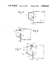
- FIG. 1 shows a cross section of the wave absorber according to the present invention
- FIG. 2 shows a perspective view of the structure of FIG. 1,
- FIG. 3 is a perspective view of another embodiment of the present invention.
- FIG. 4 is a cross section of still another embodiment according to the present invention.
- FIG. 5 is a cross section of still another embodiment according to the present invention.
- FIG. 6 is a cross section of still another embodiment according to the present invention.
- FIG. 7 is a cross section of still another embodiment according to the present invention.
- FIG. 8 and FIG. 9 show cross sections of the modification which is coupled with the previous embodiments.
- FIG. 10 shows curves of the dielectric constants and the magnetic permeability of the wave absorber in a described experiment with
- FIGS. 11(a), 11(b) and 11(c) show the structure of the wave absorber devices experimented in the present invention.
- FIGS. 12(a), 12(b) and 12(c) show curves of the experimented characteristics of the present invention.
- FIG. 1 shows the cross section of the wave absorber device according to the present invention
- FIG. 2 is the perspective view of FIG. 1.
- the reference numeral 1 is a chamber in which food is cooked.
- the numeral 1a is a wall which encloses the chamber 1 except of a front opening which is closed by a door 2.
- the door 2 may open and/or close the chamber 1.
- the door 2 is provided with a frame 3 at the peripheral portion of the door 2.
- the frame 3 faces with the end 6 of the wall 1a with a small gap.
- Said frame 3 has a choke cavity 7 which resonates with the length approximately 1/4 wavelength of the fundamental frequency of a magnetron oscillator.
- the cavity 7 has, in the present embodiment, a plurality of periorically spaced tines 10 which function to shorten the length of the cavity, and widen the operational frequency band of the cavity.
- the cavity 7 attenuates energy of microwaves which leak through the gap between the chamber wall and the door from the point A at the inner surface 8 of the wall 1a.
- the basic idea of the present invention is to mount a wave absorber at the portion where the flux density is high in a cavity.
- the flux density at the edge of the tines 10 is maximum in the cavity 7, therefore the folded flanges 11 are provided at the end of the tines 10, and on said flanges 11, a longitudinal elastic single wave absorber member 12 which bridges a plurality of tines is mounted as shown by the dotted line in FIG. 2.
- the absorber member 12 is made of the mixture of (ferrite powder and/or carbonil iron powder), and (plastics, and/or natural gum), or the mixture of the above mixture and carbon powder.
- the wave absorber 12 contacts with the end 6 of the wall 1a, or at least faces with said end 6 with a small gap which is far less than the wavelength of 12 GHz, when the door is closed so that the cavity 1 is electrically and magnetically closed completely.
- the thickness L 1 of the wave absorber is in the range between 1 mm and 2 mm
- the width L 2 of the wave absorber is in the range between 6 mm and 8 mm.
- the length of the cavity is 1/4 wavelenth, and so, the fundamental microwave frequency which leaks from the point A at the corner of the chamber is considerably attenuated.
- the wave absorber 12 As the wave absorber 12 is mounted at the extreme edge of the tines 10, the leakage of the waves from the cavity 7 is attenuated. It should be appreciated that the wave absorber is in particular effective as it is mounted at the portion where the flux is at peak value in the cavity. The wave absorber is effective not only for the attenuation of the fundamental frequency (2450 MHz), but also the attenuation of the harmonics up to 12 GHz. Thus, the noise from a microwave oven which could affect satellite communication is effectively attenuated.
- FIG. 3 is the modification of the structure of FIG. 2.
- the feature of FIG. 3 is the use of an intermediate conductive plate 15 instead of a plurality of periodic tines 10 of FIG. 2.
- the intermediate plate 15 has a folded portion at the extreme end of the same, and at that folded portion, a longitudinal wave absorber 12 is attached.
- the wave absorber is elastic so that the gap between the chamber and the door is completely closed.
- FIG. 4 is another embodiment of the present invention.
- the cavity 7B at the peripheral portion of the door 2 has the intermediate conductor 20 which may be composed of a plurality of tines like FIG. 2, or a bulk plate like FIG. 3.
- the conductor 20 has the folded portion at the extreme end of a same, and the wave absorber 12 is mounted at said folded portion.
- the second wave absorber 22 which is made of the same material as that of the absorber 12 is attached at the edge of the external wall 22a of the cavity 7B.
- the wave absorber 22 contacts directly with the wall 1a or at least faces with the wall 1a with the small gap as compared with the wavelength of 12 GHz.
- FIG. 4 is very effective to attenuate the leakage of wave energy, since the wave absorber is attached not only at the edge of the intermediate conductor 20, but also at the edge of the external wall 22a of the cavity.
- FIG. 5 is still another embodiment of the present invention.
- the important feature of the embodiment of FIG. 5 is the location of the wave absorber 27 which is mounted at the edge of the inner wall of the cavity 7C.
- the conductive frame 25 which is the inner wall of the chamber 1 extends to the side 6. That conductive frame 25 contacts with the wall of the cavity 7C which is mounted at the peripheral portion of the door 2.
- the length of the cavity 7C is approximately 1/4 wavelength of the fundamental frequency.
- the intermediate plate or the intermediate tines is not provided. However, it should be noted that the absence of the intermediate plate is not the important feature of the embodiment, and that intermediate plate may also be mounted in the cavity.
- the cavity 7C has a opening which faces with the wall 6 of the chamber 1.
- the inner wall of the cavity 7C has the fold 26, to which the wave absorber 27 is attached.
- the wave absorber 27 contacts essentially with the wall 6 or 25 of the chamber 1 so that the gap between the chamber and the door is closed. It should be noted that the flux density is at the peak value at the edge of the inner wall, or the folded portion 26, therefore, the wave absorber 27 which is located at the portion where the flux density is at peak value attenuates substantially not only the fundamental frequency but also the harmonic frequencies.
- FIG. 6 is the modification of the embodiment of FIG. 5.
- the feature of FIG. 6 is the presence of the additional wave absorber 28 at the edge of the outer wall of the cavity 7C.
- wave absorbers are mounted at an edge of a cavity, and the entrance or the opening of the cavity is closed by non-magnetic material like plastics, or said entrance is even open. It is preferable that an entrance of a cavity is sealed by dielectric material so that dust collecting in a cavity is prevented.
- the wave absorber is mounted at the portion where the flux density in the cavity is at the peak value. In a pratical embodiment, the wave absorber is mounted at the edge of an intermediate conductor (FIGS. 1 through 3), or at the edge of an outer wall of a cavity (FIGS. 4 and 6), or at the edge of an inner wall of a cavity (FIGS. 5 and 6).
- the wave absorber may be mounted at two edges (FIGS.
- the wave absorber may even be mounted at three edges (outer wall, intermediate plate, and inner wall).
- the wave absorber is mounted at many points of a cavity, the effect of attenuation of leakage is high, so, the number of waves absorbed is the trade-off between the cost of a device and the required attenuation of leakage.
- one or two absorbers are enough for a microwave oven which does not disturb satellite communication.
- FIG. 7 is a cross section of still another embodiment of the present invention.
- the important feature of the embodiment of FIG. 7 is that the wave absorber is located not only at the edge of the cavity wall, but also at the inside of the cavity.
- the chamber 71 for putting food to be cooked has a frame with the wall 71a.
- the chamber 71 has the opening which is closed by a door 72.
- the door 72 has the conductive shield mesh on the opening, therefore, no wave energy leaks through the opening.
- the leakage path is the small gap between the wall 75 of the door 72 and the wall 76 of the chamber 71.
- the leakage through said small gap is attenuated by the cavity 73 located at the peripheral portion of the door 72, and the wave absorber according to the present invention.
- the cavity 73 has the elongated empty space which is closed by the first outer wall 73a which is perpendicular to the door 72 at the extreme end of the door 72, the second wall 73b which is parallel to the door 72 and is coupled with said first wall 73a, and the third inner wall 73c which is provided between said second wall 73b and the door 72, and the wall 75 of the door 72.
- the opening is closed by the closing member 74 made of dielectric material, like plastics.
- the whole body of the cavity 73 is covered with the dielectric cover 74a.
- the first wall 73a at the extreme end of the cavity 73 has the folded flange 77 at the edge of the wall 73a, and the wave absorber 78 is attached to the folded flange 77 and the inner wall of the wall 73a.
- the wave absorber 78 is elongated, and is L-shaped, having the first arm 78a, and the second arm 78b.
- the first arm 78a of the wave absorber closes the small gap between the cavity wall 75 and the wall 76 of the chamber.
- the second arm 78b of the wave absorber extends into the inner surface of the cavity 73 as shown in the figure.
- FIG. 7 is effective because the wave absorber is mounted not only outside of the cavity but also inside of the cavity. As the flux density in the cavity is at peak value around the edge of the wall or the folded portion 77, the leakage flux is absorbed by the absorber, and further, the leakage flux through the gap between the walls 75 and 76 is also absorbed because the absorber 78a closes said gap.
- the material of the wave absorber 78 may be similar to that of the previous embodiments.
- FIGS. 8 and 9 show the modification of previous embodiments, and the feature of FIGS. 8 and 9 is the integral structure of a wave absorber and dielectric cover of a cavity.
- the chamber 81 of a microwave oven has a door 82 which closes the opening of the chamber 81.
- the door 82 has the conductive frame 83 at the peripheral portion of the door 82.
- the wall 85 of the frame 83 faces with the wall 86 of the chamber 81 with a small gap.
- the frame 83 provides a cavity 87 which resonates with the fundamental frequency (2450 MHz) of a microwave oven.
- the opening or the entrance of the cavity 87 is covered with the dielectric cover 91 which is integral with the wave absorber 90.
- the cover 90 is made of plastics, and is fixed to the cavity 87 through for instance adhesive means.
- the cover 91 has a hand 91a at the extreme end of the cover 91, and said hand 91a has a first arm 91b, a second arm 91b and a third arm 91d.
- the third arm 91d has a fold 91e.
- the wave absorber 90 locates at the end of the wall of the cavity 87. Therefore, the operation of the wave absorber 90 is similar to the wave absorber 28 in FIG. 6, or the wave absorber 78a in FIG. 7.
- the numeral 85 is the wall of the cavity 87, 86 and 88 are the walls of the chamber 81. The gap between the walls 85 and 86 is the leakage path, and the leakage through said path is prevented by the present invention.
- FIG. 9 is the modification of FIG. 8, and the feature of FIG. 9 is the location of a wave absorber 90A which is located at another edge D of the opening of the cavity 87A.
- the wave absorber 90A is integral with the dielectric cover 91A which covers the opening of the cavity 87A.
- the numeral 83A is the frame of the cavity 87A, and 92A is the plastics decoration which covers the cavity 87A.
- the electrical operation of FIG. 9 is similar to that of FIG. 5.
- FIGS. 8 and 9 are advantageous in manufacturing process. Since a dielectric cover (91, 91A) and a wave absorber (90, 90A) is half assembled first, the manufacturing process of an oven is simplified.
- the horizontal axis in FIG. 10 shows frequency between 1 GHz and 20 GHz.
- FIGS. 11(a), 11(b) and 11(c) show models of the structure of a wave absorber.
- a wave absorber A is located at the edge of the outer wall of a cavity.
- a wave absorber B is located at both the edge of the outer wall of the cavity, and the inner surface of the outer wall of the cavity.
- a wave absorber C is located at the inner surface of the outer wall, the edge of the outer wall, and in the gap between the cavity and the chamber wall.
- FIGS. 12(a), 12(b) and 12(c) show experimental curves.
- FIG. 12(a) is the curve resulting from the structure of FIG. 11(a)
- FIG. 12(b) is the curve resulting from the structure of FIG. 11(b)
- FIG. 12(c) is the curve resulting from the structure of FIG. 11(c).
- the external curves B show the data in which no wave absorber is mounted
- the inner curves A show the data in which a wave absorber is mounted.
- the data is taken on the horizontal plane where a microwave oven is placed around the direction of 360 degrees.
- the front direction is indicated by 0 degrees
- the rear direction is indicated by 180 degrees.
- the coplanar circles show the strength of noise power between 40 dBpW and 70 dBpW.
- the allowable upper limit of the noise power in the CISPR standard is 57 dBpW.
Abstract
A microwave absorber device for a microwave heater having a chamber for cooking with an opening, and a door for closing the opening with a small gap which is a leakage path between the door and the wall of the chamber. The door is provided with a choke cavity at the peripheral portions of the same, the choke cavity having an approximate 1/4 wavelength of length, and an entrance facing the leakage path. The choke cavity is provided with wave absorber which includes ferrite, and/or carbon, at an edge of the entrance or an edge of the cavity. The wave absorber closes also the leakage path. The entrance itself is sealed by dielectric material.
Description
The present invention relates to the improvement of an electro-magnetic wave absorber device, or the improvement of a device for preventing the leakage of waves. The present invention is used, for instance, for preventing leakage of wave energy in a microwave heater, for example, a microwave oven.
Conventionally, an absorber device for microwave leakage in a microwave oven has three absorber means. The first one is a metal contact spring which provides the conductive contact between the body and the door to close the door completely. The second one is a choke cavity with 1/4 wavelength for absorbing waves which leak through said conductive contact. The third one is a ferrite absorber provided at the outlet of the leakage path for absorbing the rest of the leakage.
The present applicant obtained the U.S. Pat. No. 4,525,614 (the corresponding UK Pat. No. 2 122 059, French Pat. No. 82 19333, German Pat. No. 32 42 125). That patent has the feature that the opening of the choke cavity is covered with ferrite material. That patent is excellent as far as the fundamental oscillation frequency (2450 MHz) of a microwave oven concerned.
However, it has been lately become desirable that not only the fundamental frequency but also the harmonic frequencies (for instance the frequency around 12 GHz) are sufficiently attenuated so that a satellite broadcast is not disturbed by a microwave oven. Further, the high frequency noise between 1 GHz and 18 GHz is subject to control.
Accordingly, the leakage of not only the fundamental frequency but also the harmonics must be prevented.
A prior choke cavity which resonates with the fundamental frequency is useless to prevent the subsequent harmonics.
It is an object of the present invention to overcome the disadvantages and limitations of a prior electro-magnetic wave absorber device by providing a new and improved absorber device.
It is also an object of the present invention to provide an electro-magnetic wave absorber device which is effective not only for the fundamental frequency but also for the harmonic frequencies.
The above and other objects are attained by an electro-magnetic wave absorber device comprising a chamber in which food to be cooked is put; a door for closing an opening of said chamber made of electro-magnetic shielding material; a cavity provided at peripheral portions of said door so that an opening of said cavity faces with a wall of the chamber; said cavity being provided with a wave absorber at an edge of a wall of the cavity so that a gap between the door and the wall of the chamber is closed by said wave absorber, and said wave absorber is comprised of ferrite powder.
The foregoing and other objects, features, and attendant advantages of the present invention will be appreciated as the same become better understood by means of the following description and accompanying drawings wherein;
FIG. 1 shows a cross section of the wave absorber according to the present invention,
FIG. 2 shows a perspective view of the structure of FIG. 1,
FIG. 3 is a perspective view of another embodiment of the present invention,
FIG. 4 is a cross section of still another embodiment according to the present invention,
FIG. 5 is a cross section of still another embodiment according to the present invention,
FIG. 6 is a cross section of still another embodiment according to the present invention,
FIG. 7 is a cross section of still another embodiment according to the present invention,
FIG. 8 and FIG. 9 show cross sections of the modification which is coupled with the previous embodiments.
FIG. 10 shows curves of the dielectric constants and the magnetic permeability of the wave absorber in a described experiment with,
FIGS. 11(a), 11(b) and 11(c) show the structure of the wave absorber devices experimented in the present invention, and
FIGS. 12(a), 12(b) and 12(c) show curves of the experimented characteristics of the present invention.
FIG. 1 shows the cross section of the wave absorber device according to the present invention, and FIG. 2 is the perspective view of FIG. 1. In those figures, the reference numeral 1 is a chamber in which food is cooked. The numeral 1a is a wall which encloses the chamber 1 except of a front opening which is closed by a door 2. Of course, the door 2 may open and/or close the chamber 1. The door 2 is provided with a frame 3 at the peripheral portion of the door 2. The frame 3 faces with the end 6 of the wall 1a with a small gap.
Said frame 3 has a choke cavity 7 which resonates with the length approximately 1/4 wavelength of the fundamental frequency of a magnetron oscillator. The cavity 7 has, in the present embodiment, a plurality of periorically spaced tines 10 which function to shorten the length of the cavity, and widen the operational frequency band of the cavity.
The cavity 7 attenuates energy of microwaves which leak through the gap between the chamber wall and the door from the point A at the inner surface 8 of the wall 1a.
The basic idea of the present invention is to mount a wave absorber at the portion where the flux density is high in a cavity. In our analysis, the flux density at the edge of the tines 10 is maximum in the cavity 7, therefore the folded flanges 11 are provided at the end of the tines 10, and on said flanges 11, a longitudinal elastic single wave absorber member 12 which bridges a plurality of tines is mounted as shown by the dotted line in FIG. 2. The absorber member 12 is made of the mixture of (ferrite powder and/or carbonil iron powder), and (plastics, and/or natural gum), or the mixture of the above mixture and carbon powder.
The wave absorber 12 contacts with the end 6 of the wall 1a, or at least faces with said end 6 with a small gap which is far less than the wavelength of 12 GHz, when the door is closed so that the cavity 1 is electrically and magnetically closed completely. In the preferred embodiment, the thickness L1 of the wave absorber is in the range between 1 mm and 2 mm, and the width L2 of the wave absorber is in the range between 6 mm and 8 mm.
In the above structure, the length of the cavity is 1/4 wavelenth, and so, the fundamental microwave frequency which leaks from the point A at the corner of the chamber is considerably attenuated.
As the wave absorber 12 is mounted at the extreme edge of the tines 10, the leakage of the waves from the cavity 7 is attenuated. It should be appreciated that the wave absorber is in particular effective as it is mounted at the portion where the flux is at peak value in the cavity. The wave absorber is effective not only for the attenuation of the fundamental frequency (2450 MHz), but also the attenuation of the harmonics up to 12 GHz. Thus, the noise from a microwave oven which could affect satellite communication is effectively attenuated.
FIG. 3 is the modification of the structure of FIG. 2. The feature of FIG. 3 is the use of an intermediate conductive plate 15 instead of a plurality of periodic tines 10 of FIG. 2. The intermediate plate 15 has a folded portion at the extreme end of the same, and at that folded portion, a longitudinal wave absorber 12 is attached. Preferably, the wave absorber is elastic so that the gap between the chamber and the door is completely closed.
FIG. 4 is another embodiment of the present invention. In the figure, the cavity 7B at the peripheral portion of the door 2 has the intermediate conductor 20 which may be composed of a plurality of tines like FIG. 2, or a bulk plate like FIG. 3. The conductor 20 has the folded portion at the extreme end of a same, and the wave absorber 12 is mounted at said folded portion. Further, in the embodiment of FIG. 4, the second wave absorber 22 which is made of the same material as that of the absorber 12 is attached at the edge of the external wall 22a of the cavity 7B. The wave absorber 22 contacts directly with the wall 1a or at least faces with the wall 1a with the small gap as compared with the wavelength of 12 GHz.
The embodiment of FIG. 4 is very effective to attenuate the leakage of wave energy, since the wave absorber is attached not only at the edge of the intermediate conductor 20, but also at the edge of the external wall 22a of the cavity.
FIG. 5 is still another embodiment of the present invention. The important feature of the embodiment of FIG. 5 is the location of the wave absorber 27 which is mounted at the edge of the inner wall of the cavity 7C. In the embodiment of FIG. 5, the conductive frame 25 which is the inner wall of the chamber 1 extends to the side 6. That conductive frame 25 contacts with the wall of the cavity 7C which is mounted at the peripheral portion of the door 2. The length of the cavity 7C is approximately 1/4 wavelength of the fundamental frequency. In the embodiment of FIG. 5, the intermediate plate or the intermediate tines is not provided. However, it should be noted that the absence of the intermediate plate is not the important feature of the embodiment, and that intermediate plate may also be mounted in the cavity.
The cavity 7C has a opening which faces with the wall 6 of the chamber 1. The inner wall of the cavity 7C has the fold 26, to which the wave absorber 27 is attached. The wave absorber 27 contacts essentially with the wall 6 or 25 of the chamber 1 so that the gap between the chamber and the door is closed. It should be noted that the flux density is at the peak value at the edge of the inner wall, or the folded portion 26, therefore, the wave absorber 27 which is located at the portion where the flux density is at peak value attenuates substantially not only the fundamental frequency but also the harmonic frequencies.
FIG. 6 is the modification of the embodiment of FIG. 5. The feature of FIG. 6 is the presence of the additional wave absorber 28 at the edge of the outer wall of the cavity 7C.
As described above, according to the present invention, wave absorbers are mounted at an edge of a cavity, and the entrance or the opening of the cavity is closed by non-magnetic material like plastics, or said entrance is even open. It is preferable that an entrance of a cavity is sealed by dielectric material so that dust collecting in a cavity is prevented. The wave absorber is mounted at the portion where the flux density in the cavity is at the peak value. In a pratical embodiment, the wave absorber is mounted at the edge of an intermediate conductor (FIGS. 1 through 3), or at the edge of an outer wall of a cavity (FIGS. 4 and 6), or at the edge of an inner wall of a cavity (FIGS. 5 and 6). The wave absorber may be mounted at two edges (FIGS. 4 and 6), or the wave absorber may even be mounted at three edges (outer wall, intermediate plate, and inner wall). When the wave absorber is mounted at many points of a cavity, the effect of attenuation of leakage is high, so, the number of waves absorbed is the trade-off between the cost of a device and the required attenuation of leakage. In our experiment, one or two absorbers are enough for a microwave oven which does not disturb satellite communication.
FIG. 7 is a cross section of still another embodiment of the present invention. The important feature of the embodiment of FIG. 7 is that the wave absorber is located not only at the edge of the cavity wall, but also at the inside of the cavity.
In FIG. 7, the chamber 71 for putting food to be cooked has a frame with the wall 71a. The chamber 71 has the opening which is closed by a door 72. The door 72 has the conductive shield mesh on the opening, therefore, no wave energy leaks through the opening. The leakage path is the small gap between the wall 75 of the door 72 and the wall 76 of the chamber 71. The leakage through said small gap is attenuated by the cavity 73 located at the peripheral portion of the door 72, and the wave absorber according to the present invention.
The cavity 73 has the elongated empty space which is closed by the first outer wall 73a which is perpendicular to the door 72 at the extreme end of the door 72, the second wall 73b which is parallel to the door 72 and is coupled with said first wall 73a, and the third inner wall 73c which is provided between said second wall 73b and the door 72, and the wall 75 of the door 72. The opening is closed by the closing member 74 made of dielectric material, like plastics. The whole body of the cavity 73 is covered with the dielectric cover 74a.
The first wall 73a at the extreme end of the cavity 73 has the folded flange 77 at the edge of the wall 73a, and the wave absorber 78 is attached to the folded flange 77 and the inner wall of the wall 73a. The wave absorber 78 is elongated, and is L-shaped, having the first arm 78a, and the second arm 78b. The first arm 78a is attached to the folded flange 77, and has the thickness L1 =3 mm. The first arm 78a of the wave absorber closes the small gap between the cavity wall 75 and the wall 76 of the chamber. The second arm 78b of the wave absorber extends into the inner surface of the cavity 73 as shown in the figure.
The embodiment of FIG. 7 is effective because the wave absorber is mounted not only outside of the cavity but also inside of the cavity. As the flux density in the cavity is at peak value around the edge of the wall or the folded portion 77, the leakage flux is absorbed by the absorber, and further, the leakage flux through the gap between the walls 75 and 76 is also absorbed because the absorber 78a closes said gap.
It should be noted of course that when an additional absorber is mounted at another edge of the cavity (edge of the wall 75), the effect is further improved.
The material of the wave absorber 78 may be similar to that of the previous embodiments.
FIGS. 8 and 9 show the modification of previous embodiments, and the feature of FIGS. 8 and 9 is the integral structure of a wave absorber and dielectric cover of a cavity.
In FIG. 8, the chamber 81 of a microwave oven has a door 82 which closes the opening of the chamber 81. The door 82 has the conductive frame 83 at the peripheral portion of the door 82. The wall 85 of the frame 83 faces with the wall 86 of the chamber 81 with a small gap. The frame 83 provides a cavity 87 which resonates with the fundamental frequency (2450 MHz) of a microwave oven.
The opening or the entrance of the cavity 87 is covered with the dielectric cover 91 which is integral with the wave absorber 90. The cover 90 is made of plastics, and is fixed to the cavity 87 through for instance adhesive means. The cover 91 has a hand 91a at the extreme end of the cover 91, and said hand 91a has a first arm 91b, a second arm 91b and a third arm 91d. Preferably, the third arm 91d has a fold 91e. When assembled, the wave absorber 90 locates at the end of the wall of the cavity 87. Therefore, the operation of the wave absorber 90 is similar to the wave absorber 28 in FIG. 6, or the wave absorber 78a in FIG. 7. The numeral 85 is the wall of the cavity 87, 86 and 88 are the walls of the chamber 81. The gap between the walls 85 and 86 is the leakage path, and the leakage through said path is prevented by the present invention.
FIG. 9 is the modification of FIG. 8, and the feature of FIG. 9 is the location of a wave absorber 90A which is located at another edge D of the opening of the cavity 87A. Of course the wave absorber 90A is integral with the dielectric cover 91A which covers the opening of the cavity 87A. The numeral 83A is the frame of the cavity 87A, and 92A is the plastics decoration which covers the cavity 87A. The electrical operation of FIG. 9 is similar to that of FIG. 5.
The embodiments of FIGS. 8 and 9 are advantageous in manufacturing process. Since a dielectric cover (91, 91A) and a wave absorber (90, 90A) is half assembled first, the manufacturing process of an oven is simplified.
Next, some experimental results of the present invention are shown in accordance with FIGS. 10 through 12.
FIG. 10 shows the curves of the real parts of the dielectric constant ε' and the magnetic permeability μ', and the imaginary part of the dielectric constant ε" and the permeability μ" of the wave absorber which is used in the experiment (ε=ε'+jε",μ=μ'+μ"). The horizontal axis in FIG. 10 shows frequency between 1 GHz and 20 GHz.
FIGS. 11(a), 11(b) and 11(c) show models of the structure of a wave absorber. In FIG. 11(a), a wave absorber A is located at the edge of the outer wall of a cavity. In FIG. 11(b), a wave absorber B is located at both the edge of the outer wall of the cavity, and the inner surface of the outer wall of the cavity. In FIG. 11(c), a wave absorber C is located at the inner surface of the outer wall, the edge of the outer wall, and in the gap between the cavity and the chamber wall.
FIGS. 12(a), 12(b) and 12(c) show experimental curves. FIG. 12(a) is the curve resulting from the structure of FIG. 11(a), FIG. 12(b) is the curve resulting from the structure of FIG. 11(b), and FIG. 12(c) is the curve resulting from the structure of FIG. 11(c). In those curves of FIGS. 12(a) through 12(c), the external curves B show the data in which no wave absorber is mounted, and the inner curves A show the data in which a wave absorber is mounted. The data is taken on the horizontal plane where a microwave oven is placed around the direction of 360 degrees. The front direction is indicated by 0 degrees, and the rear direction is indicated by 180 degrees. The coplanar circles show the strength of noise power between 40 dBpW and 70 dBpW. The allowable upper limit of the noise power in the CISPR standard is 57 dBpW.
It should be appreciated that the curve of FIG. 12(c) is the best, and the curve of FIG. 12(b) is satisfactory. In the curve of FIG. 12(a), the noise power of the curve A is considerably decreased as compared with that of the curve B.
From the foregoing it will now be apparent that a new and improved microwave absorber device has been discovered. It should be understood of course that the embodiments disclosed are merely illustrative and are not intended to limit the scope of the invention. Reference should be made to the appended claims, therefore, rather than the specification as indicating the scope of the invention.
Claims (15)
1. In a microwave heating apparatus having
a chamber in which food to be cooked is put,
a microwave generating means,
a door for closing an opening of said chamber made of electro-magnetic shielding material,
a choke cavity provided at peripheral portions of said door so that a opening of said choke cavity faces with a wall of the chamber,
characterized in that
said choke cavity is provided with wave absorber mounted in the opening plane of the choke cavity and extends over only a portion of the opening of the choke cavity, and
said wave absorber is comprised of ferrite material.
2. A microwave apparatus according to claim 1, wherein said wave absorber is provided at a edge of an intermediate plate in said choke cavity.
3. A microwave apparatus according to claim 2, wherein said intermediate plate is separated into a plurality of elongated tines.
4. A microwave apparatus according to claim 1, wherein said wave absorber is provided at an edge of an outer wall of said choke cavity.
5. A microwave apparatus according to claim 4, wherein said wave absorber extends into inner surface of the choke cavity.
6. A microwave apparatus according to claim 1, wherein said wave absorber is provided at an edge of an inner wall of said choke cavity.
7. A microwave apparatus according to claim 1, wherein said wave absorber is provided at an edge of an intermediate plate and an edge of an outer wall of the choke cavity.
8. A microwave apparatus according to claim 1, wherein said wave absorber is provided at an edge of an outer wall and an edge of an inner wall of the choke cavity.
9. A microwave apparatus according to claim 1, wherein said wave absorber is integral with dielectric cover means which closes entrance of the choke cavity.
10. A microwave apparatus according to claim 9, wherein said wave absorber is adhered to the cover means which is made of plastics.
11. A microwave apparatus according to claim 1, wherein a wall of the choke cavity has a fold at an extreme end of the wall, and a wave absorber is adhered on said fold.
12. A microwave apparatus according to claim 1, wherein said wave absorber closes a gap between said choke cavity and a wall of said chamber.
13. A microwave apparatus according to claim 1 wherein said wave absorber extends over only a small fractional portion of the opening of the choke cavity.
14. A microwave apparatus according to claim 1 wherein said wave absorber is an elongated strip with a thickness in the range between 1 mm and 2 mm, and a width in the range between 6 mm and 8 mm.
15. A microwave apparatus according to claim 1 wherein said ferrite material is a ferrite powder.
Applications Claiming Priority (5)
| Application Number | Priority Date | Filing Date | Title |
|---|---|---|---|
| JP1985000005U JPH0127598Y2 (en) | 1985-01-04 | 1985-01-04 | |
| JP60-000005[U] | 1985-01-04 | ||
| JP60-162635[U]JPX | 1985-10-23 | ||
| JP16263685U JPS6270393U (en) | 1985-10-23 | 1985-10-23 | |
| JP16263585U JPS6270392U (en) | 1985-10-23 | 1985-10-23 |
Publications (1)
| Publication Number | Publication Date |
|---|---|
| US4689460A true US4689460A (en) | 1987-08-25 |
Family
ID=27274264
Family Applications (1)
| Application Number | Title | Priority Date | Filing Date |
|---|---|---|---|
| US06/812,961 Expired - Fee Related US4689460A (en) | 1985-01-04 | 1985-12-24 | Absorber device for microwave leakage |
Country Status (5)
| Country | Link |
|---|---|
| US (1) | US4689460A (en) |
| DE (1) | DE3546370A1 (en) |
| FR (1) | FR2575893A1 (en) |
| GB (1) | GB2170379B (en) |
| IT (1) | IT1203519B (en) |
Cited By (8)
| Publication number | Priority date | Publication date | Assignee | Title |
|---|---|---|---|---|
| US5070223A (en) * | 1989-03-01 | 1991-12-03 | Colasante David A | Microwave reheatable clothing and toys |
| US5075525A (en) * | 1990-06-25 | 1991-12-24 | Goldstar Co., Ltd. | Wave shielding device for microwave oven |
| KR100575687B1 (en) | 2004-07-27 | 2006-05-03 | 엘지전자 주식회사 | Microwave interception apparatus of microwave oven |
| KR100575686B1 (en) | 2004-07-27 | 2006-05-03 | 엘지전자 주식회사 | Micro wave interception apparatus of microwave oven |
| EP1744595A2 (en) * | 2005-07-13 | 2007-01-17 | LG Electronics Inc. | Microwave cooker with prevention of microwave leakage |
| US20110297673A1 (en) * | 2009-04-03 | 2011-12-08 | Electrolux Home Products Corporation N.V. | wave choke system for a door of a microwave oven |
| CN104854956A (en) * | 2013-01-25 | 2015-08-19 | 伊莱克斯家用产品股份有限公司 | A microwave oven or a multifunctional oven with microwave heating function |
| US9380651B2 (en) * | 2010-12-23 | 2016-06-28 | Eastman Chemical Company | Microwave choke system for use in heating articles under vacuum |
Families Citing this family (1)
| Publication number | Priority date | Publication date | Assignee | Title |
|---|---|---|---|---|
| GB2196520B (en) * | 1986-08-07 | 1990-01-04 | Hitachi Heating Appl | Microwave heating apparatus |
Citations (8)
| Publication number | Priority date | Publication date | Assignee | Title |
|---|---|---|---|---|
| US3633564A (en) * | 1970-11-23 | 1972-01-11 | Tokyo Shibaura Electric Co | High-frequency sealing device |
| US3742176A (en) * | 1969-06-26 | 1973-06-26 | Tdk Electronics Co Ltd | Method for preventing the leakage of microwave energy from microwave heating oven |
| US3809843A (en) * | 1970-06-01 | 1974-05-07 | Gen Corp | Microwave heating apparatus |
| US4046983A (en) * | 1975-09-03 | 1977-09-06 | Tdk Electronics Co., Ltd. | Microwave heating oven having seal means for preventing the leakage of microwave energy |
| US4347420A (en) * | 1979-09-11 | 1982-08-31 | Matsushita Electric Industrial Co., Ltd. | Microwave seal structure in microwave oven |
| US4475023A (en) * | 1981-09-25 | 1984-10-02 | Hitachi Heating Appliances Co., Ltd. | Microwave heating apparatus with fundamental and second higher harmonic chokes |
| US4523069A (en) * | 1983-10-24 | 1985-06-11 | General Electric Company | Microwave oven door seal |
| US4525614A (en) * | 1982-05-28 | 1985-06-25 | Tdk Corporation | Absorber device for microwave leakage |
Family Cites Families (14)
| Publication number | Priority date | Publication date | Assignee | Title |
|---|---|---|---|---|
| US3666904A (en) * | 1971-04-12 | 1972-05-30 | Bowmar Tic Inc | Microwave oven and door structure for minimizing leakage |
| FR2138822B1 (en) * | 1971-05-20 | 1976-06-11 | Matsushita Electric Ind Co Ltd | |
| DE2224661B2 (en) * | 1972-05-19 | 1974-12-12 | Matsushita Electric Industrial Co., Ltd., Kadoma, Osaka (Japan) | Microwave oven elimination in: 2264616 and elimination in: 2264617 and elimination in: 2264618 and elimination in: 2264619 |
| SE357247B (en) * | 1971-10-19 | 1973-06-18 | Philips Svenska Ab | |
| BE791916A (en) * | 1971-11-30 | 1973-03-16 | Raytheon Co | HIGH-FREQUENCY ENERGY HEATING APPLIANCE |
| US3879595A (en) * | 1973-01-08 | 1975-04-22 | Tappan Co | Microwave oven door seal |
| ZA742105B (en) * | 1973-05-02 | 1975-03-26 | Amana Refrigeration Inc | Multilength microwave oven choketype energy seal |
| US3846608A (en) * | 1974-02-11 | 1974-11-05 | Litton Systems Inc | High temperature resistant door seal for a microwave oven |
| DE2705983C2 (en) * | 1977-02-12 | 1982-12-09 | Litton Industries, Inc., 90210 Beverly Hills, Calif. | Combination microwave cooking equipment |
| US4166207A (en) * | 1977-05-31 | 1979-08-28 | Whirlpool Corporation | Microwave generating device--door seal |
| US4146769A (en) * | 1977-08-24 | 1979-03-27 | Litton Systems, Inc. | Microwave oven door |
| JPS5743599U (en) * | 1980-08-26 | 1982-03-10 | ||
| US4313044A (en) * | 1980-11-05 | 1982-01-26 | General Electric Company | Slot configuration for choke seal |
| US4539433A (en) * | 1982-11-24 | 1985-09-03 | Tdk Corporation | Electromagnetic shield |
-
1985
- 1985-12-24 US US06/812,961 patent/US4689460A/en not_active Expired - Fee Related
- 1985-12-31 DE DE3546370A patent/DE3546370A1/en not_active Ceased
-
1986
- 1986-01-03 FR FR8600047A patent/FR2575893A1/en not_active Withdrawn
- 1986-01-03 IT IT67002/86A patent/IT1203519B/en active
- 1986-01-03 GB GB08600049A patent/GB2170379B/en not_active Expired
Patent Citations (8)
| Publication number | Priority date | Publication date | Assignee | Title |
|---|---|---|---|---|
| US3742176A (en) * | 1969-06-26 | 1973-06-26 | Tdk Electronics Co Ltd | Method for preventing the leakage of microwave energy from microwave heating oven |
| US3809843A (en) * | 1970-06-01 | 1974-05-07 | Gen Corp | Microwave heating apparatus |
| US3633564A (en) * | 1970-11-23 | 1972-01-11 | Tokyo Shibaura Electric Co | High-frequency sealing device |
| US4046983A (en) * | 1975-09-03 | 1977-09-06 | Tdk Electronics Co., Ltd. | Microwave heating oven having seal means for preventing the leakage of microwave energy |
| US4347420A (en) * | 1979-09-11 | 1982-08-31 | Matsushita Electric Industrial Co., Ltd. | Microwave seal structure in microwave oven |
| US4475023A (en) * | 1981-09-25 | 1984-10-02 | Hitachi Heating Appliances Co., Ltd. | Microwave heating apparatus with fundamental and second higher harmonic chokes |
| US4525614A (en) * | 1982-05-28 | 1985-06-25 | Tdk Corporation | Absorber device for microwave leakage |
| US4523069A (en) * | 1983-10-24 | 1985-06-11 | General Electric Company | Microwave oven door seal |
Cited By (12)
| Publication number | Priority date | Publication date | Assignee | Title |
|---|---|---|---|---|
| US5070223A (en) * | 1989-03-01 | 1991-12-03 | Colasante David A | Microwave reheatable clothing and toys |
| US5075525A (en) * | 1990-06-25 | 1991-12-24 | Goldstar Co., Ltd. | Wave shielding device for microwave oven |
| KR100575687B1 (en) | 2004-07-27 | 2006-05-03 | 엘지전자 주식회사 | Microwave interception apparatus of microwave oven |
| KR100575686B1 (en) | 2004-07-27 | 2006-05-03 | 엘지전자 주식회사 | Micro wave interception apparatus of microwave oven |
| EP1744595A2 (en) * | 2005-07-13 | 2007-01-17 | LG Electronics Inc. | Microwave cooker with prevention of microwave leakage |
| US20070012689A1 (en) * | 2005-07-13 | 2007-01-18 | Lg Electronics Inc. | Microwave cooker |
| EP1744595A3 (en) * | 2005-07-13 | 2008-10-29 | LG Electronics Inc. | Microwave cooker with prevention of microwave leakage |
| US7592573B2 (en) | 2005-07-13 | 2009-09-22 | Lg Electronics Inc. | Microwave cooker comprising a multi-stage choke seal |
| US20110297673A1 (en) * | 2009-04-03 | 2011-12-08 | Electrolux Home Products Corporation N.V. | wave choke system for a door of a microwave oven |
| US9380651B2 (en) * | 2010-12-23 | 2016-06-28 | Eastman Chemical Company | Microwave choke system for use in heating articles under vacuum |
| CN104854956A (en) * | 2013-01-25 | 2015-08-19 | 伊莱克斯家用产品股份有限公司 | A microwave oven or a multifunctional oven with microwave heating function |
| CN104854956B (en) * | 2013-01-25 | 2017-03-08 | 伊莱克斯家用产品股份有限公司 | Microwave oven or the multifunctional oven with microwave heating function |
Also Published As
| Publication number | Publication date |
|---|---|
| FR2575893A1 (en) | 1986-07-11 |
| IT8667002A0 (en) | 1986-01-03 |
| GB2170379A (en) | 1986-07-30 |
| GB2170379B (en) | 1988-12-21 |
| IT1203519B (en) | 1989-02-15 |
| GB8600049D0 (en) | 1986-02-12 |
| DE3546370A1 (en) | 1986-07-17 |
Similar Documents
| Publication | Publication Date | Title |
|---|---|---|
| CA1102883A (en) | Microwave generating device--door seal | |
| US4659891A (en) | Microwave oven having an electromagnetic energy seal | |
| US4046983A (en) | Microwave heating oven having seal means for preventing the leakage of microwave energy | |
| KR950000247B1 (en) | Apparatus for shielding microwave for electronic range | |
| US4689460A (en) | Absorber device for microwave leakage | |
| US4700034A (en) | Electromagnetic energy seal of a microwave oven | |
| JP3892458B2 (en) | microwave | |
| US4525614A (en) | Absorber device for microwave leakage | |
| US3879595A (en) | Microwave oven door seal | |
| JP2972305B2 (en) | Electromagnetic shielding body and enclosure for electromagnetic shielding | |
| JPS6225920Y2 (en) | ||
| KR970005100B1 (en) | High frequency sealing apparatus for a microwave oven | |
| KR100291895B1 (en) | Electromagnetic wave shielding device of microwave oven | |
| KR950000309Y1 (en) | High-friquency leakage interference device for magnetron | |
| KR101125562B1 (en) | High frequency shielding structure of microwave oven | |
| JPS645839Y2 (en) | ||
| JPH0127598Y2 (en) | ||
| JPS645840Y2 (en) | ||
| RU97103691A (en) | SUPERWIDE-BAND ELECTROMAGNETIC WAVE DETECTOR | |
| JPS6341757Y2 (en) | ||
| KR20210132498A (en) | Microwave oven with device for shielding electromagnetic wave | |
| JPH0145112Y2 (en) | ||
| JPS6341756Y2 (en) | ||
| KR100202628B1 (en) | Leakage interception apparatus of microwave for microwave oven | |
| JPS5934076Y2 (en) | Radio wave leakage prevention device for high frequency heating equipment |
Legal Events
| Date | Code | Title | Description |
|---|---|---|---|
| AS | Assignment |
Owner name: TDK CORPORATION, 13-1, NIHONBASHI 1-CHOME, CHU0-KU Free format text: ASSIGNMENT OF ASSIGNORS INTEREST.;ASSIGNORS:ISHINO, KEN;HASHIMOTO, YASUO;HAYASHI, KATUHIKO;AND OTHERS;REEL/FRAME:004500/0249 Effective date: 19851220 |
|
| FPAY | Fee payment |
Year of fee payment: 4 |
|
| REMI | Maintenance fee reminder mailed | ||
| LAPS | Lapse for failure to pay maintenance fees | ||
| STCH | Information on status: patent discontinuation |
Free format text: PATENT EXPIRED DUE TO NONPAYMENT OF MAINTENANCE FEES UNDER 37 CFR 1.362 |